US11227721B2 - Electronic component - Google Patents
Electronic component Download PDFInfo
- Publication number
- US11227721B2 US11227721B2 US15/821,998 US201715821998A US11227721B2 US 11227721 B2 US11227721 B2 US 11227721B2 US 201715821998 A US201715821998 A US 201715821998A US 11227721 B2 US11227721 B2 US 11227721B2
- Authority
- US
- United States
- Prior art keywords
- electrode
- layer
- disposed
- conductor
- element body
- Prior art date
- Legal status (The legal status is an assumption and is not a legal conclusion. Google has not performed a legal analysis and makes no representation as to the accuracy of the status listed.)
- Active, expires
Links
Images


Classifications
-
- H—ELECTRICITY
- H01—ELECTRIC ELEMENTS
- H01G—CAPACITORS; CAPACITORS, RECTIFIERS, DETECTORS, SWITCHING DEVICES, LIGHT-SENSITIVE OR TEMPERATURE-SENSITIVE DEVICES OF THE ELECTROLYTIC TYPE
- H01G4/00—Fixed capacitors; Processes of their manufacture
- H01G4/002—Details
- H01G4/228—Terminals
- H01G4/232—Terminals electrically connecting two or more layers of a stacked or rolled capacitor
- H01G4/2325—Terminals electrically connecting two or more layers of a stacked or rolled capacitor characterised by the material of the terminals
-
- H—ELECTRICITY
- H01—ELECTRIC ELEMENTS
- H01F—MAGNETS; INDUCTANCES; TRANSFORMERS; SELECTION OF MATERIALS FOR THEIR MAGNETIC PROPERTIES
- H01F17/00—Fixed inductances of the signal type
- H01F17/04—Fixed inductances of the signal type with magnetic core
-
- H—ELECTRICITY
- H01—ELECTRIC ELEMENTS
- H01F—MAGNETS; INDUCTANCES; TRANSFORMERS; SELECTION OF MATERIALS FOR THEIR MAGNETIC PROPERTIES
- H01F27/00—Details of transformers or inductances, in general
- H01F27/28—Coils; Windings; Conductive connections
- H01F27/29—Terminals; Tapping arrangements for signal inductances
- H01F27/292—Surface mounted devices
-
- H—ELECTRICITY
- H01—ELECTRIC ELEMENTS
- H01B—CABLES; CONDUCTORS; INSULATORS; SELECTION OF MATERIALS FOR THEIR CONDUCTIVE, INSULATING OR DIELECTRIC PROPERTIES
- H01B1/00—Conductors or conductive bodies characterised by the conductive materials; Selection of materials as conductors
- H01B1/20—Conductive material dispersed in non-conductive organic material
- H01B1/22—Conductive material dispersed in non-conductive organic material the conductive material comprising metals or alloys
-
- H—ELECTRICITY
- H01—ELECTRIC ELEMENTS
- H01F—MAGNETS; INDUCTANCES; TRANSFORMERS; SELECTION OF MATERIALS FOR THEIR MAGNETIC PROPERTIES
- H01F1/00—Magnets or magnetic bodies characterised by the magnetic materials therefor; Selection of materials for their magnetic properties
- H01F1/01—Magnets or magnetic bodies characterised by the magnetic materials therefor; Selection of materials for their magnetic properties of inorganic materials
- H01F1/03—Magnets or magnetic bodies characterised by the magnetic materials therefor; Selection of materials for their magnetic properties of inorganic materials characterised by their coercivity
- H01F1/0302—Magnets or magnetic bodies characterised by the magnetic materials therefor; Selection of materials for their magnetic properties of inorganic materials characterised by their coercivity characterised by unspecified or heterogeneous hardness or specially adapted for magnetic hardness transitions
- H01F1/0311—Compounds
- H01F1/0313—Oxidic compounds
- H01F1/0315—Ferrites
-
- H—ELECTRICITY
- H01—ELECTRIC ELEMENTS
- H01F—MAGNETS; INDUCTANCES; TRANSFORMERS; SELECTION OF MATERIALS FOR THEIR MAGNETIC PROPERTIES
- H01F17/00—Fixed inductances of the signal type
- H01F17/0006—Printed inductances
- H01F17/0013—Printed inductances with stacked layers
-
- H—ELECTRICITY
- H01—ELECTRIC ELEMENTS
- H01F—MAGNETS; INDUCTANCES; TRANSFORMERS; SELECTION OF MATERIALS FOR THEIR MAGNETIC PROPERTIES
- H01F27/00—Details of transformers or inductances, in general
- H01F27/28—Coils; Windings; Conductive connections
- H01F27/29—Terminals; Tapping arrangements for signal inductances
-
- H—ELECTRICITY
- H01—ELECTRIC ELEMENTS
- H01F—MAGNETS; INDUCTANCES; TRANSFORMERS; SELECTION OF MATERIALS FOR THEIR MAGNETIC PROPERTIES
- H01F27/00—Details of transformers or inductances, in general
- H01F27/28—Coils; Windings; Conductive connections
- H01F27/32—Insulating of coils, windings, or parts thereof
- H01F27/324—Insulation between coil and core, between different winding sections, around the coil; Other insulation structures
-
- H—ELECTRICITY
- H01—ELECTRIC ELEMENTS
- H01G—CAPACITORS; CAPACITORS, RECTIFIERS, DETECTORS, SWITCHING DEVICES, LIGHT-SENSITIVE OR TEMPERATURE-SENSITIVE DEVICES OF THE ELECTROLYTIC TYPE
- H01G13/00—Apparatus specially adapted for manufacturing capacitors; Processes specially adapted for manufacturing capacitors not provided for in groups H01G4/00 - H01G11/00
- H01G13/006—Apparatus or processes for applying terminals
-
- H—ELECTRICITY
- H01—ELECTRIC ELEMENTS
- H01G—CAPACITORS; CAPACITORS, RECTIFIERS, DETECTORS, SWITCHING DEVICES, LIGHT-SENSITIVE OR TEMPERATURE-SENSITIVE DEVICES OF THE ELECTROLYTIC TYPE
- H01G4/00—Fixed capacitors; Processes of their manufacture
- H01G4/002—Details
- H01G4/228—Terminals
- H01G4/232—Terminals electrically connecting two or more layers of a stacked or rolled capacitor
-
- H—ELECTRICITY
- H01—ELECTRIC ELEMENTS
- H01G—CAPACITORS; CAPACITORS, RECTIFIERS, DETECTORS, SWITCHING DEVICES, LIGHT-SENSITIVE OR TEMPERATURE-SENSITIVE DEVICES OF THE ELECTROLYTIC TYPE
- H01G4/00—Fixed capacitors; Processes of their manufacture
- H01G4/002—Details
- H01G4/228—Terminals
- H01G4/252—Terminals the terminals being coated on the capacitive element
-
- H—ELECTRICITY
- H01—ELECTRIC ELEMENTS
- H01G—CAPACITORS; CAPACITORS, RECTIFIERS, DETECTORS, SWITCHING DEVICES, LIGHT-SENSITIVE OR TEMPERATURE-SENSITIVE DEVICES OF THE ELECTROLYTIC TYPE
- H01G4/00—Fixed capacitors; Processes of their manufacture
- H01G4/30—Stacked capacitors
-
- H—ELECTRICITY
- H03—ELECTRONIC CIRCUITRY
- H03H—IMPEDANCE NETWORKS, e.g. RESONANT CIRCUITS; RESONATORS
- H03H7/00—Multiple-port networks comprising only passive electrical elements as network components
- H03H7/42—Networks for transforming balanced signals into unbalanced signals and vice versa, e.g. baluns
- H03H7/425—Balance-balance networks
- H03H7/427—Common-mode filters
-
- H—ELECTRICITY
- H05—ELECTRIC TECHNIQUES NOT OTHERWISE PROVIDED FOR
- H05K—PRINTED CIRCUITS; CASINGS OR CONSTRUCTIONAL DETAILS OF ELECTRIC APPARATUS; MANUFACTURE OF ASSEMBLAGES OF ELECTRICAL COMPONENTS
- H05K1/00—Printed circuits
- H05K1/02—Details
- H05K1/03—Use of materials for the substrate
- H05K1/0306—Inorganic insulating substrates, e.g. ceramic, glass
-
- H—ELECTRICITY
- H01—ELECTRIC ELEMENTS
- H01F—MAGNETS; INDUCTANCES; TRANSFORMERS; SELECTION OF MATERIALS FOR THEIR MAGNETIC PROPERTIES
- H01F17/00—Fixed inductances of the signal type
- H01F17/0006—Printed inductances
- H01F2017/0066—Printed inductances with a magnetic layer
-
- H—ELECTRICITY
- H01—ELECTRIC ELEMENTS
- H01F—MAGNETS; INDUCTANCES; TRANSFORMERS; SELECTION OF MATERIALS FOR THEIR MAGNETIC PROPERTIES
- H01F17/00—Fixed inductances of the signal type
- H01F2017/0093—Common mode choke coil
-
- H—ELECTRICITY
- H01—ELECTRIC ELEMENTS
- H01F—MAGNETS; INDUCTANCES; TRANSFORMERS; SELECTION OF MATERIALS FOR THEIR MAGNETIC PROPERTIES
- H01F17/00—Fixed inductances of the signal type
- H01F17/04—Fixed inductances of the signal type with magnetic core
- H01F2017/048—Fixed inductances of the signal type with magnetic core with encapsulating core, e.g. made of resin and magnetic powder
-
- H—ELECTRICITY
- H01—ELECTRIC ELEMENTS
- H01G—CAPACITORS; CAPACITORS, RECTIFIERS, DETECTORS, SWITCHING DEVICES, LIGHT-SENSITIVE OR TEMPERATURE-SENSITIVE DEVICES OF THE ELECTROLYTIC TYPE
- H01G4/00—Fixed capacitors; Processes of their manufacture
- H01G4/002—Details
- H01G4/018—Dielectrics
- H01G4/06—Solid dielectrics
- H01G4/08—Inorganic dielectrics
- H01G4/12—Ceramic dielectrics
-
- H—ELECTRICITY
- H03—ELECTRONIC CIRCUITRY
- H03H—IMPEDANCE NETWORKS, e.g. RESONANT CIRCUITS; RESONATORS
- H03H1/00—Constructional details of impedance networks whose electrical mode of operation is not specified or applicable to more than one type of network
- H03H2001/0021—Constructional details
- H03H2001/0057—Constructional details comprising magnetic material
-
- H—ELECTRICITY
- H03—ELECTRONIC CIRCUITRY
- H03H—IMPEDANCE NETWORKS, e.g. RESONANT CIRCUITS; RESONATORS
- H03H1/00—Constructional details of impedance networks whose electrical mode of operation is not specified or applicable to more than one type of network
- H03H2001/0021—Constructional details
- H03H2001/0085—Multilayer, e.g. LTCC, HTCC, green sheets
-
- H—ELECTRICITY
- H05—ELECTRIC TECHNIQUES NOT OTHERWISE PROVIDED FOR
- H05K—PRINTED CIRCUITS; CASINGS OR CONSTRUCTIONAL DETAILS OF ELECTRIC APPARATUS; MANUFACTURE OF ASSEMBLAGES OF ELECTRICAL COMPONENTS
- H05K2201/00—Indexing scheme relating to printed circuits covered by H05K1/00
- H05K2201/10—Details of components or other objects attached to or integrated in a printed circuit board
- H05K2201/10007—Types of components
- H05K2201/1006—Non-printed filter
-
- H—ELECTRICITY
- H05—ELECTRIC TECHNIQUES NOT OTHERWISE PROVIDED FOR
- H05K—PRINTED CIRCUITS; CASINGS OR CONSTRUCTIONAL DETAILS OF ELECTRIC APPARATUS; MANUFACTURE OF ASSEMBLAGES OF ELECTRICAL COMPONENTS
- H05K2201/00—Indexing scheme relating to printed circuits covered by H05K1/00
- H05K2201/10—Details of components or other objects attached to or integrated in a printed circuit board
- H05K2201/10613—Details of electrical connections of non-printed components, e.g. special leads
- H05K2201/10621—Components characterised by their electrical contacts
- H05K2201/10636—Leadless chip, e.g. chip capacitor or resistor
-
- H—ELECTRICITY
- H05—ELECTRIC TECHNIQUES NOT OTHERWISE PROVIDED FOR
- H05K—PRINTED CIRCUITS; CASINGS OR CONSTRUCTIONAL DETAILS OF ELECTRIC APPARATUS; MANUFACTURE OF ASSEMBLAGES OF ELECTRICAL COMPONENTS
- H05K3/00—Apparatus or processes for manufacturing printed circuits
- H05K3/30—Assembling printed circuits with electric components, e.g. with resistors
- H05K3/32—Assembling printed circuits with electric components, e.g. with resistors electrically connecting electric components or wires to printed circuits
- H05K3/34—Assembling printed circuits with electric components, e.g. with resistors electrically connecting electric components or wires to printed circuits by soldering
- H05K3/341—Surface mounted components
- H05K3/3431—Leadless components
- H05K3/3442—Leadless components having edge contacts, e.g. leadless chip capacitors, chip carriers
-
- Y—GENERAL TAGGING OF NEW TECHNOLOGICAL DEVELOPMENTS; GENERAL TAGGING OF CROSS-SECTIONAL TECHNOLOGIES SPANNING OVER SEVERAL SECTIONS OF THE IPC; TECHNICAL SUBJECTS COVERED BY FORMER USPC CROSS-REFERENCE ART COLLECTIONS [XRACs] AND DIGESTS
- Y02—TECHNOLOGIES OR APPLICATIONS FOR MITIGATION OR ADAPTATION AGAINST CLIMATE CHANGE
- Y02P—CLIMATE CHANGE MITIGATION TECHNOLOGIES IN THE PRODUCTION OR PROCESSING OF GOODS
- Y02P70/00—Climate change mitigation technologies in the production process for final industrial or consumer products
- Y02P70/50—Manufacturing or production processes characterised by the final manufactured product
Definitions
- the present invention relates to an electronic component.
- Known electronic components include an element body and an external electrode disposed on the element body (for example, see Japanese Unexamined Patent Publication No. 2014-143387).
- the external electrode includes a sintered metal layer disposed on a surface of the element body and a conductive resin layer disposed to cover the sintered metal layer.
- An object of one and another aspects of the present invention is to provide an electronic component that suppresses peeling of the conductive resin layer.
- the conductive resin layer is in contact with the element body.
- the conductive resin layer is disposed to cover the sintered metal layer, and thus an edge of the conductive resin layer is in contact with the element body.
- the conductive resin layer typically includes a conductive material (for example, metal powder) and a resin (for example, a thermosetting resin) and thus has lower adhesive strength with an element body than a resin including no conductive material.
- an external force acting on the electronic component from the electronic device may act as a stress on the external electrode.
- the external force acts on the electronic component as the substrate is bent. Since the stress acting on the external electrode tends to act on a portion of the external electrode, in particular, the portion being disposed on a principal surface that is arranged to constitute a mounting surface, the conductive resin layer included in the external electrode may be peeled off from the element body.
- the conductive resin layer is peeled off from the element body, mounting strength of the electronic component may be decreased.
- moisture may infiltrate into the electronic component from between the element body and the conductive resin layer, and electrical characteristics of the electronic component may be deteriorated.
- An electronic component includes an element body, an external electrode, and a resin film having electrical insulation properties.
- the element body has a principal surface and a side surface.
- the principal surface is arranged to constitute a mounting surface.
- the principal surface and the side surface are adjacent to each other.
- the external electrode includes a first electrode portion disposed on the principal surface and a second electrode portion disposed on the side surface.
- the resin film is disposed on the principal surface and is in contact with the principal surface.
- Each of the first electrode portion and the second electrode portion includes a conductive resin layer disposed on the element body.
- a conductive resin layer included in the first electrode portion is disposed on the resin film and is in contact with the resin film.
- the conductive resin layer included in the first electrode portion is in contact with the resin film in contact with the principal surface of the element body.
- the resin film is interposed between the conductive resin layer included in the first electrode portion and the principal surface of the element body.
- the resin film does not contain a conductive material and has high adhesive strength with the element body.
- the conductive resin layer contains a resin, and thus has high adhesive strength with the resin film. Therefore, in the one aspect, the conductive resin layer included in the first electrode portion tends not to peel off.
- the electronic component according to the one aspect may include an internal conductor.
- the internal conductor is disposed in the element body and includes an end exposed at the side surface.
- the second electrode portion may include a sintered metal layer connected with an end of the internal conductor.
- the sintered metal layer may be disposed on the side surface and may be in contact with the side surface.
- the conductive resin layer included in the second electrode portion may be disposed on the element body in such a manner that the sintered metal layer is disposed between the element body and the conductive resin layer included in the second electrode portion.
- the internal conductor is electrically connected with the conductive resin layer through the sintered metal layer. Therefore, in this embodiment, connection strength between the internal conductor and the external electrode is high and the internal conductor and the external electrode are reliably electrically connected, as compared with in an electronic component in which an internal conductor and a conductive resin layer are directly connected.
- the resin film may cover an edge of the sintered metal layer and may be in contact with the edge. In which case, the end of the resin film is sandwiched between the sintered metal layer and the conductive resin layer. Therefore, the resin film tends not to peel off.
- the element body may include a side surface opposing the side surface.
- the external electrode may include a plurality of terminal electrodes disposed on each of both end portions of the element body in a direction in which the pair of side surfaces opposes each other.
- each of the terminal electrode is not formed to cover the entire side surface.
- the area of each of the terminal electrodes must be small. Therefore, the area of the conductive resin layer is small, and the adhesive strength of the conductive resin layer may be decreased.
- the conductive resin layer included in the first electrode portion is in contact with the resin film in contact with the principal surface of the element body. Therefore, the conductive resin layer included in the first electrode portion tends not to peel off.
- the resin film may be in contact with the conductive resin layers included in the first electrode portions of at least two adjacent terminal electrodes. In which case, formation of the resin film is easy.
- the resin film may be provided for each terminal electrode and may be in contact with the conductive resin layer included in the first electrode portion of the corresponding terminal electrode. In which case, the amount of resin used for forming the resin film is reduced.
- a resin for example, a thermosetting resin
- adhesive strength of the resin to the surface of the element body is improved by the anchor effect as the surface of the element body becomes rougher.
- adhesive strength between a conductive resin layer included in an external electrode and the surface of the element body is improved.
- the conductive resin layer tends to peel off from the element body even though the surface of the magnetic portion is rough. This may be caused because the anchor effect tends not to be exhibited between the magnetic portion and the conductive resin layer.
- the external electrode including the conductive resin layer may also peel off from the element body, and moisture may infiltrate into the element body from between the element body and the conductive resin layer. If the moisture infiltrates into the element body, electrical characteristics of the electronic component may be deteriorated.
- the inventors of the present invention have conducted intensive studies on a configuration in which the external electrode tends not to peel off from the element body even when the conductive resin layer is disposed on the magnetic portion made of a ferrite material. As a result, the present inventors have found the following configuration. An amorphous glass layer is formed on the surface of the magnetic portion and the amorphous glass layer is disposed between an edge of the conductive resin layer included in the external electrode and the surface of the magnetic portion. In this configuration, although a surface of the amorphous glass layer is smoother than the surface of the magnetic portion, peeling of the conductive resin layer from the element body is suppressed, as compared with a multilayer common mode filter having the conductive resin layer directly disposed on the magnetic portion.
- An electronic component includes an element body, an amorphous glass layer, and an external electrode.
- the element body includes a magnetic portion made of a ferrite material.
- the amorphous glass layer is formed on a surface of the magnetic portion.
- the external electrode includes a conductive resin layer disposed on the element body. The amorphous glass layer is disposed between an edge of the conductive resin layer and the surface of the magnetic portion.
- the amorphous glass layer is disposed between the edge of the conductive resin layer and the surface of the magnetic portion. Therefore, peeling of the conductive resin layer from the element body is suppressed.
- the element body may include a principal surface including at least a part of the surface of the magnetic portion and a side surface adjacent to the principal surface.
- the external electrode may include a first electrode portion disposed on the principal surface and a second electrode portion disposed on the side surface.
- the amorphous glass layer may be formed on the principal surface.
- the conductive resin layer may be included in the first electrode portion and the second electrode portion.
- the edge of the conductive resin layer may be included in the first electrode portion.
- the amorphous glass layer may be disposed between the edge of the conductive resin layer and the principal surface.
- the electronic component according to this embodiment When the electronic component according to this embodiment is mounted on an electronic device in a state where the principal surface opposes the electronic device, an external force acting on the electronic component from the electronic device tends to act as a stress on the first electrode portion. If the external force acts on the first electrode portion, the conductive resin layer included in the first electrode portion may peel off from the element body (amorphous glass layer). However, in this embodiment, the amorphous glass layer is disposed between the edge of the conductive resin layer and the principal surface. Therefore, even when the electronic component is mounted on the electronic device, the conductive resin layer tends not to peel off from the element body (amorphous glass layer).
- the electronic component according to the another aspect may include an insulating resin layer.
- the insulating resin layer may be disposed between the amorphous glass layer and the edge of the conductive resin layer.
- the edge of the conductive resin layer may be in contact with the insulating resin layer.
- the conductive resin layer typically contains a conductive material (for example, a metal powder) and a resin (for example, a thermosetting resin).
- the insulating resin layer not containing a conductive material has higher adhesive strength to the amorphous glass coat layer than the conductive resin layer. Therefore, when the edge of the conductive resin layer is in contact with the insulating resin layer, peeling of the conductive resin layer from the element body (amorphous glass layer) is further suppressed.
- the external electrode may include a plurality of terminal electrodes.
- Each of the terminal electrodes includes the conductive resin layer.
- the contact area between the conductive resin layer of each of the terminal electrodes and the element body is small, as compared with when the number of terminal electrodes is one.
- the conductive resin layer may peel off from the element body.
- the amorphous glass layer is disposed between the edge of the conductive resin layer and the surface of the magnetic portion, and thus the conductive resin layer tends not to peel off from the element body (amorphous glass layer).
- the external electrode may include a sintered metal layer made of Ag.
- the conductive resin layer may be disposed on the sintered metal layer and may be in contact with the sintered metal layer.
- surface roughness of the amorphous glass layer may be smaller than surface roughness of the magnetic portion.
- FIG. 1 is a perspective view illustrating a multilayer common mode filter according to a first embodiment
- FIG. 2 is a plan view illustrating the multilayer common mode filter according to the first embodiment
- FIG. 3 is an exploded perspective view illustrating a configuration of an element body
- FIG. 4 is a diagram illustrating a cross-sectional configuration of a first terminal electrode, a second terminal electrode, and a resin film
- FIG. 5 is a diagram illustrating a cross-sectional configuration of a third terminal electrode, a fourth terminal electrode, and a resin film
- FIG. 6 is a diagram illustrating a mounting structure of the multilayer common mode filter according to the first embodiment
- FIG. 7 is a diagram illustrating a mounting structure of the multilayer common mode filter according to the first embodiment
- FIG. 8 is a plan view illustrating a multilayer common mode filter according to a modification of the first embodiment
- FIG. 9 is a plan view illustrating a multilayer common mode filter according to a modification of the first embodiment
- FIG. 10 is a plan view illustrating a multilayer common mode filter according to a modification of the first embodiment
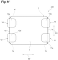
- FIG. 11 is a plan view illustrating a multilayer common mode filter according to a modification of the first embodiment
- FIG. 12 is a diagram illustrating a cross-sectional configuration of a first terminal electrode, a second terminal electrode, and a resin layer
- FIG. 13 is a diagram illustrating a cross-sectional configuration of a third terminal electrode, a fourth terminal electrode, and a resin layer;
- FIG. 14 is a perspective view illustrating a multilayer common mode filter according to a second embodiment
- FIG. 15 is a plan view illustrating the multilayer common mode filter according to the second embodiment.
- FIG. 16 is an exploded perspective view illustrating a configuration of an element body
- FIG. 17 is a diagram illustrating a cross-sectional configuration of the multilayer common mode filter according to the second embodiment
- FIG. 18 is a diagram illustrating a cross-sectional configuration of the multilayer common mode filter according to the second embodiment
- FIG. 19A is a view illustrating a surface of a magnetic portion
- FIG. 19B is a view illustrating a surface of an amorphous glass coat layer
- FIG. 20 is a diagram illustrating a mounting structure of the multilayer common mode filter according to the second embodiment.
- FIG. 21 is a diagram illustrating a mounting structure of the multilayer common mode filter according to the second embodiment.
- FIG. 22 is a diagram illustrating a cross-sectional configuration of a multilayer common mode filter according to a modification of the second embodiment
- FIG. 23 is a diagram illustrating a cross-sectional configuration of a multilayer common mode filter according to a modification of the second embodiment.
- FIG. 24 is a diagram illustrating a cross-sectional configuration of a multilayer common mode filter according to a modification of the second embodiment.
- FIG. 1 is a perspective view illustrating a multilayer common mode filter according to a first embodiment.
- FIG. 2 is a plan view illustrating the multilayer common mode filter according to the first embodiment.
- FIG. 3 is an exploded perspective view illustrating a configuration of an element body.
- FIG. 4 is a diagram illustrating a cross-sectional configuration of a first terminal electrode, a second terminal electrode, and a resin film.
- FIG. 5 is a diagram illustrating a cross-sectional configuration of a third terminal electrode, a fourth terminal electrode, and a resin film.
- an electronic component is the multilayer common mode filter CF 1 , for example.
- the multilayer common mode filter CF 1 includes an element body 1 and an external electrode.
- the external electrode includes a first terminal electrode 11 , a second terminal electrode 12 , a third terminal electrode 13 , and a fourth terminal electrode 14 .
- the first terminal electrode 11 , the second terminal electrode 12 , the third terminal electrode 13 , and the fourth terminal electrode 14 are disposed on an external surface of the element body 1 .
- the multilayer common mode filter CF 1 is mounted on an electronic device (for example, a circuit board or an electronic component) by soldering in such a manner that the first terminal electrode 11 , the second terminal electrode 12 , the third terminal electrode 13 , and the fourth terminal electrode 14 are separately connected to signal lines.
- the element body 1 has a rectangular parallelepiped shape.
- the element body 1 includes a first principal surface 1 a and a second principal surface 1 b opposing each other, a first side surface 1 c and a second side surface 1 d opposing each other, and a third side surface 1 e and a fourth side surface if opposing each other.
- a direction in which the first principal surface 1 a and the second principal surface 1 b oppose each other is a first direction D 1 .
- a direction in which the first side surface 1 c and the second side surface 1 d oppose each other is a second direction D 2 .
- a direction in which the third side surface 1 e and the fourth side surface 1 f oppose each other is a third direction D 3 .
- the first direction D 1 is a height direction of the element body 1 .
- the second direction D 2 is a longitudinal direction of the element body 1 .
- the third direction D 3 is a width direction of the element body 1 .
- the rectangular parallelepiped shape includes a shape of a rectangular parallelepiped in which a corner portion and a ridge portion are chamfered and a shape of a rectangular parallelepiped in which a corner portion and a ridge portion are rounded.
- the first side surface 1 c and the second side surface 1 d extend in the first direction D 1 to connect the first principal surface 1 a and the second principal surface 1 b .
- the first side surface 1 c and the second side surface 1 d are adjacent to the first principal surface 1 a and are also adjacent to the second principal surface 1 b .
- the first side surface 1 c and the second side surface 1 d also extend in the third direction D 3 .
- the third direction D 3 is also a short side direction of the first principal surface 1 a and the second principal surface 1 b.
- the third side surface 1 e and the fourth side surface if extend in the first direction D 1 to connect the first principal surface 1 a and the second principal surface 1 b .
- the first side surface 1 c and the second side surface 1 d are adjacent to the first principal surface 1 a and are also adjacent to the second principal surface 1 b .
- the third side surface 1 e and the fourth side surface 1 f also extend in the second direction D 2 .
- the second direction D 2 is also a long side direction of the first principal surface 1 a and the second principal surface 1 b.
- the element body 1 includes a non-magnetic portion 3 and a pair of magnetic portions 5 .
- the pair of magnetic portions 5 is disposed to sandwich the non-magnetic portion 3 in the first direction D 1 .
- the element body 1 includes a plurality of laminated insulating layers.
- a plurality of non-magnetic layers 4 are laminated.
- the non-magnetic portion 3 includes the plurality of laminated non-magnetic layers 4 .
- a plurality of magnetic layers 6 are laminated.
- Each of the magnetic portions 5 includes the plurality of laminated magnetic layers 6 .
- the plurality of insulating layers include the plurality of non-magnetic layers 4 and the plurality of magnetic layers 6 .
- Each of the non-magnetic layers 4 is configured by a sintered body of a ceramic green sheet including a non-magnetic material, for example.
- the non-magnetic material is a Cu—Zn based ferrite material, a dielectric material, or a glass ceramic material, for example.
- Each of the magnetic layers 6 is configured by a sintered body of a ceramic green sheet including a magnetic material, for example.
- the magnetic material is a Ni—Cu—Zn based ferrite material, a Ni—Cu—Zn—Mg based ferrite material, or a Ni—Cu based ferrite material, for example.
- the first direction D 1 (the direction in which the first principal surface 1 a and the second principal surface 1 b oppose each other) is matched with a direction in which the plurality of insulating layers (the plurality of non-magnetic layers 4 and the plurality of magnetic layers 6 ) are laminated.
- the direction in which the plurality of insulating layers are laminated is simply referred to as a “lamination direction”.
- the multilayer common mode filter CF 1 includes a first coil conductor 21 , a second coil conductor 22 , a third coil conductor 23 , and a fourth coil conductor 24 in the non-magnetic portion 3 .
- the first coil conductor 21 , the second coil conductor 22 , the third coil conductor 23 , and the fourth coil conductor 24 are internal conductors disposed in the element body 1 .
- the first to fourth coil conductors 21 to 24 include a conductive material (for example, Ag or Pd).
- the first to fourth coil conductors 21 to 24 are configured as sintered bodies of conductive paste including a conductive material (for example, Ag powder or Pd powder).
- the first coil conductor 21 has a spiral shape and is disposed between a pair of the non-magnetic layers 4 adjacent to each other in the lamination direction. One end (outside end) 21 a of the first coil conductor 21 is exposed at the first side surface 1 c . Another end (inside end) 21 b of the first coil conductor 21 is connected to a first pad conductor 41 .
- the first pad conductor 41 is located at the same layer as the first coil conductor 21 . In the present embodiment, the first coil conductor 21 and the first pad conductor 41 are integrally formed.
- the second coil conductor 22 has a spiral shape and is disposed between a pair of the non-magnetic layers 4 adjacent to each other in the lamination direction. One end (outside end) 22 a of the second coil conductor 22 is exposed at the second side surface 1 d . Another end (inside end) 22 b of the second coil conductor 22 is connected to a second pad conductor 42 .
- the second pad conductor 42 is located at the same layer as the second coil conductor 22 . In the present embodiment, the second coil conductor 22 and the second pad conductor 42 are integrally formed.
- the third coil conductor 23 has a spiral shape and is disposed between a pair of the non-magnetic layers 4 adjacent to each other in the lamination direction. One end (outside end) 23 a of the third coil conductor 23 is exposed at the first side surface 1 c . Another end (inside end) 23 b of the third coil conductor 23 is connected to a third pad conductor 43 .
- the third pad conductor 43 is located at the same layer as the third coil conductor 23 . In the present embodiment, the third coil conductor 23 and the third pad conductor 43 are integrally formed.
- the fourth coil conductor 24 has a spiral shape and is disposed between a pair of the non-magnetic layers 4 adjacent to each other in the lamination direction. One end (outside end) 24 a of the fourth coil conductor 24 is exposed at the second side surface 1 d . Another end (inside end) 24 b of the fourth coil conductor 24 is connected to a fourth pad conductor 44 .
- the fourth pad conductor 44 is located at the same layer as the fourth coil conductor 24 . In the present embodiment, the fourth coil conductor 24 and the fourth pad conductor 44 are integrally formed.
- the first coil conductor 21 and the third coil conductor 23 are adjacent to each other in the lamination direction in a state where the non-magnetic layer 4 is interposed between the first coil conductor 21 and the third coil conductor 23 .
- the non-magnetic layer 4 is sandwiched between the first coil conductor 21 and the third coil conductor 23 .
- the second coil conductor 22 and the fourth coil conductor 24 are adjacent to each other in the lamination direction in a state where the non-magnetic layer 4 is interposed between the second coil conductor 22 and the fourth coil conductor 24 .
- the non-magnetic layer 4 is sandwiched between the second coil conductor 22 and the fourth coil conductor 24 .
- the third coil conductor 23 is positioned between the first coil conductor 21 and the second coil conductor 22 in the lamination direction.
- the first to fourth coil conductors 21 to 24 are disposed in the order of the first coil conductor 21 , the third coil conductor 23 , the second coil conductor 22 , and the fourth coil conductor 24 in the lamination direction.
- the first to fourth coil conductors 21 to 24 are wound in the same direction and are positioned to overlap each other, when viewed from the lamination direction.
- the first pad conductor 41 and the second pad conductor 42 are positioned to overlap each other when viewed from the lamination direction.
- a fifth pad conductor 45 is disposed between the first pad conductor 41 and the second pad conductor 42 to overlap the first and second pad conductors 41 and 42 when viewed from the lamination direction.
- the fifth pad conductor 45 is located at the same layer as the third coil conductor 23 .
- the first pad conductor 41 and the fifth pad conductor 45 are adjacent to each other in the lamination direction in a state where the non-magnetic layer 4 is interposed between the first pad conductor 41 and the fifth pad conductor 45 .
- the non-magnetic layer 4 is sandwiched between the first pad conductor 41 and the fifth pad conductor 45 .
- the fifth pad conductor 45 and the second pad conductor 42 are adjacent to each other in the lamination direction in a state where the non-magnetic layer 4 is interposed between the fifth pad conductor 45 and the second pad conductor 42 .
- the non-magnetic layer 4 is sandwiched between the fifth pad conductor 45 and the second pad conductor 42 .
- the first pad conductor 41 , the fifth pad conductor 45 , and the second pad conductor 42 are connected through a first through-hole conductor 51 .
- the first through-hole conductor 51 penetrates the non-magnetic layer 4 positioned between the first pad conductor 41 and the fifth pad conductor 45 , and the non-magnetic layer 4 positioned between the fifth pad conductor 45 and the second pad conductor 42 .
- the third pad conductor 43 and the fourth pad conductor 44 are positioned to overlap each other when viewed from the lamination direction.
- a sixth pad conductor 46 is disposed between the third pad conductor 43 and the fourth pad conductor 44 to overlap the third and fourth pad conductors 43 and 44 when viewed from the lamination direction.
- the sixth pad conductor 46 is located at the same layer as the second coil conductor 22 .
- the third pad conductor 43 and the sixth pad conductor 46 are adjacent to each other in the lamination direction in a state where the non-magnetic layer 4 is interposed between the third pad conductor 43 and the sixth pad conductor 46 .
- the non-magnetic layer 4 is sandwiched between the third pad conductor 43 and the sixth pad conductor 46 .
- the sixth pad conductor 46 and the fourth pad conductor 44 are adjacent to each other in the lamination direction in a state where the non-magnetic layer 4 is interposed between the sixth pad conductor 46 and the fourth pad conductor 44 .
- the non-magnetic layer 4 is sandwiched between the sixth pad conductor 46 and the fourth pad conductor 44 .
- the third pad conductor 43 , the sixth pad conductor 46 , and the fourth pad conductor 44 are connected through a second through-hole conductor 52 .
- the second through-hole conductor 52 penetrates the non-magnetic layer 4 positioned between the third pad conductor 43 and the sixth pad conductor 46 , and the non-magnetic layer 4 positioned between the sixth pad conductor 46 and the fourth pad conductor 44 .
- the first coil conductor 21 and the second coil conductor 22 are electrically connected through the first pad conductor 41 , the fifth pad conductor 45 , the second pad conductor 42 , and the first through-hole conductor 51 .
- the first coil conductor 21 and the second coil conductor 22 configure a first coil C 1 .
- the third coil conductor 23 and the fourth coil conductor 24 are electrically connected through the third pad conductor 43 , the sixth pad conductor 46 , the fourth pad conductor 44 , and the second through-hole conductor 52 .
- the third coil conductor 23 and the fourth coil conductor 24 configure a second coil C 2 .
- the multilayer common mode filter CF 1 includes the first coil C 1 and the second coil C 2 in the element body 1 (non-magnetic portion 3 ).
- the first coil C 1 and the second coil C 2 are disposed in the non-magnetic portion 3 in such a manner that the first coil conductor 21 and the third coil conductor 23 are adjacent to each other in the lamination direction, the third coil conductor 23 and the second coil conductor 22 are adjacent to each other in the lamination direction, and the second coil conductor 22 and the fourth coil conductor 24 are adjacent to each other in the lamination direction.
- the first coil C 1 and the second coil C 2 are arranged to be magnetically coupled to each other.
- the fifth and sixth pad conductors 45 and 46 and the first and second through-hole conductors 51 and 52 include a conductive material (for example, Ag or Pd).
- the fifth and sixth pad conductors 45 and 46 and the first and second through-hole conductors 51 and 52 are configured as a sintered body of conductive paste containing a conductive material (for example, Ag powder or Pd powder).
- the first and second through-hole conductors 51 and 52 are formed by sintering conductive paste filled in through-holes formed in ceramic green sheets that configure the corresponding non-magnetic layers 4 .
- the first terminal electrode 11 and the third terminal electrode 13 are disposed on the first side surface 1 c side of the element body 1 .
- the first terminal electrode 11 and the third terminal electrode 13 are disposed on one end portion of the element body 1 in the second direction D 2 .
- the first terminal electrode 11 and the third terminal electrode 13 are disposed on the first side surface 1 c to cover a part of the first side surface 1 c along the first direction D 1 , and are disposed on a part of the first principal surface 1 a and a part of the second principal surface 1 b .
- the first terminal electrode 11 is positioned close to the third side surface 1 e .
- the third terminal electrode 13 is positioned close to the fourth side surface 1 f.
- the second terminal electrode 12 and the fourth terminal electrode 14 are disposed on the second side surface 1 d side of the element body 1 .
- the second terminal electrode 12 and the fourth terminal electrode 14 are disposed on another end portion of the element body 1 in the second direction D 2 .
- the second terminal electrode 12 and the fourth terminal electrode 14 are disposed on the second side surface 1 d to cover a part of the second side surface 1 d along the first direction D 1 , and are disposed on a part of the first principal surface 1 a and a part of the second principal surface 1 b .
- the second terminal electrode 12 is positioned close to the third side surface 1 e .
- the fourth terminal electrode 14 is located close to the fourth side surface 1 f.
- the first terminal electrode 11 includes a plurality of electrode portions 11 a , 11 b , and 11 c .
- the electrode portion 11 a is disposed on the first principal surface 1 a .
- the electrode portion 11 b is disposed on the second principal surface 1 b .
- the electrode portion 11 c is disposed on the first side surface 1 c .
- the first terminal electrode 11 is not disposed on the second side surface 1 d , the third side surface 1 e , and the fourth side surface 1 f .
- the first terminal electrode 11 is disposed only on the three surfaces 1 a , 1 b , and 1 c .
- the electrode portions 11 a , 11 b , and 11 c adjacent to one another are electrically connected at the ridge portion of the element body 1 .
- the electrode portion 11 c covers the entire end of the first coil conductor 21 , the end being exposed at the first side surface 1 c .
- the first coil conductor 21 is connected with the electrode portion 11 c at the end exposed at the first side surface 1 c .
- the first terminal electrode 11 and the first coil conductor 21 are electrically connected to each other.
- the one end 21 a of the first coil conductor 21 functions as a connection conductor with the first terminal electrode 11 .
- the second terminal electrode 12 includes a plurality of electrode portions 12 a , 12 b , and 12 c .
- the electrode portion 12 a is disposed on the first principal surface 1 a .
- the electrode portion 12 b is disposed on the second principal surface 1 b .
- the electrode portion 12 c is disposed on the second side surface 1 d .
- the second terminal electrode 12 is not disposed on the first side surface 1 c , the third side surface 1 e , and the fourth side surface 1 f .
- the second terminal electrode 12 is disposed only on the three surfaces 1 a , 1 b , and 1 d .
- the electrode portions 12 a , 12 b , and 12 c adjacent to one another are electrically connected at the ridge portion of the element body 1 .
- the electrode portion 12 c covers the entire end of the second coil conductor 22 , the end being exposed at the second side surface 1 d .
- the second coil conductor 22 is connected with the electrode portion 12 c at the end exposed at the second side surface 1 d .
- the second terminal electrode 12 and the second coil conductor 22 are electrically connected.
- the one end 22 a of the second coil conductor 22 functions as a connection conductor with the second terminal electrode 12 .
- the third terminal electrode 13 includes a plurality of electrode portions 13 a , 13 b , and 13 c .
- the electrode portion 13 a is disposed on the first principal surface 1 a .
- the electrode portion 13 b is disposed on the second principal surface 1 b .
- the electrode portion 13 c is disposed on the first side surface 1 c .
- the third terminal electrode 13 is not disposed on the second side surface 1 d , the third side surface 1 e , and the fourth side surface 1 f .
- the third terminal electrode 13 is disposed only on the three surfaces 1 a , 1 b , and 1 c .
- the electrode portions 13 a , 13 b , and 13 c adjacent to one another are electrically connected at the ridge portion of the element body 1 .
- the electrode portion 13 c covers the entire end of the third coil conductor 23 , the end being exposed at the first side surface 1 c .
- the third coil conductor 23 is connected with the electrode portion 13 c at the end exposed at the first side surface 1 c .
- the third terminal electrode 13 and the third coil conductor 23 are electrically connected.
- the one end 23 a of the third coil conductor 23 functions as a connection conductor with the third terminal electrode 13 .
- the fourth terminal electrode 14 includes a plurality of electrode portions 14 a , 14 b , and 14 c .
- the electrode portion 14 a is disposed on the first principal surface 1 a .
- the electrode portion 14 b is disposed on the second principal surface 1 b .
- the electrode portion 14 c is disposed on the second side surface 1 d .
- the fourth terminal electrode 14 is not disposed on the first side surface 1 c , the third side surface 1 e , and the fourth side surface 1 f .
- the fourth terminal electrode 14 is disposed only on the three surfaces 1 a , 1 b , and 1 d .
- the electrode portions 14 a , 14 b , and 14 c adjacent to one another are electrically connected at the ridge portion of the element body 1 .
- the electrode portion 14 c covers the entire end of the fourth coil conductor 24 , the end being exposed at the second side surface 1 d .
- the fourth coil conductor 24 is connected with the electrode portion 14 c at the end exposed at the second side surface 1 d .
- the fourth terminal electrode 14 and the fourth coil conductor 24 are electrically connected to each other.
- the one end 24 a of the fourth coil conductor 24 functions as a connection conductor with the fourth terminal electrode 14 .
- Each of the first terminal electrode 11 , the second terminal electrode 12 , the third terminal electrode 13 , and the fourth terminal electrode 14 includes a first electrode layer E 1 , a second electrode layer E 2 , a third electrode layer E 3 , and a fourth electrode layer E 4 .
- each of the electrode portions 11 c , 12 c , 13 c , and 14 c includes the first electrode layer E 1 , the second electrode layer E 2 , the third electrode layer E 3 , and the fourth electrode layer E 4 .
- Each of the electrode portions 11 a , 11 b , 12 a , 12 b , 13 a , 13 b , 14 a , and 14 b includes the second electrode layer E 2 , the third electrode layer E 3 , and the fourth electrode layer E 4 .
- Each of the electrode portions 11 a , 11 b , 12 a , 12 b , 13 a , 13 b , 14 a , and 14 b does not include the first electrode layer E 1 .
- the fourth electrode layer E 4 configures each of uppermost layers of the first terminal electrode 11 , the second terminal electrode 12 , the third terminal electrode 13 , and the fourth terminal electrode 14 .
- the first electrode layer E 1 is formed by sintering conductive paste applied to the surface of the element body 1 (in the present embodiment, the first and second side surfaces 1 c and 1 d ).
- the first electrode layer E 1 is formed by sintering a metal component (metal powder) contained in the conductive paste.
- the first electrode layer E 1 is a sintered metal layer.
- the first electrode layer E 1 is a sintered metal layer disposed on the element body 1 .
- the first electrode layer E 1 is included in each of the electrode portions 11 c , 12 c , 13 c , and 14 c .
- the first electrode layer E 1 included in each of the electrode portions 11 c and 13 c is disposed on the first side surface 1 c and is in contact with the first side surface 1 c .
- the first electrode layer E 1 included in each of the electrode portions 12 c and 14 c is disposed on the second side surface 1 d and is in contact with the second side surface 1 d .
- the first electrode layer E 1 is not disposed on the first and second principal surfaces 1 a and 1 b.
- the first electrode layer E 1 included in the electrode portion 11 c is connected with the one end 21 a of the first coil conductor 21 .
- the first electrode layer E 1 included in the electrode portion 12 c is connected with the one end 22 a of the second coil conductor 22 .
- the first electrode layer E 1 included in the electrode portion 13 c is connected with the one end 23 a of the third coil conductor 23 .
- the first electrode layer E 1 included in the electrode portion 14 c is connected with the one end 24 a of the fourth coil conductor 24 .
- the first electrode layer E 1 is a sintered metal layer made of Ag.
- the first electrode layer E 1 may be a sintered metal layer made of Pd.
- the conductive paste includes powder made of Ag or Pd, a glass component, an organic binder, and an organic solvent.
- the second electrode layer E 2 is a conductive resin layer.
- the conductive resin layer is formed by curing a conductive resin paste, for example.
- the conductive resin paste includes a thermosetting resin, a conductive material, and an organic solvent, for example.
- the conductive material is metal powder, for example.
- the metal powder is Ag powder, for example.
- the thermosetting resin is a phenol resin, an acrylic resin, a silicone resin, an epoxy resin, or a polyimide resin, for example.
- the third electrode layer E 3 is a plating layer and is formed on the second electrode layer E 2 by a plating method.
- the third electrode layer E 3 is a Ni plating layer formed by Ni plating.
- the third electrode layer E 3 may be a Cu plating layer.
- the fourth electrode layer E 4 is a plating layer and is formed on the third electrode layer E 3 by a plating method.
- the fourth electrode layer E 4 is a Sn plating layer formed by Sn plating.
- the third electrode layer E 3 and the fourth electrode layer E 4 configure a plating layer disposed on the second electrode layer E 2 .
- the plating layer formed on the second electrode layer E 2 has a two-layer structure.
- the second electrode layer E 2 is integrally formed in each of the electrode portions 11 a to 11 c , 12 a to 12 c , 13 a to 13 c , and 14 a to 14 c .
- the third electrode layer E 3 is integrally formed in each of the electrode portions 11 a to 11 c , 12 a to 12 c , 13 a to 13 c , and 14 a to 14 c .
- the fourth electrode layer E 4 is integrally formed in each of the electrode portions 11 a to 11 c , 12 a to 12 c , 13 a to 13 c , and 14 a to 14 c.
- the entire second electrode layer E 2 is covered with the plating layer configured from the third electrode layer E 3 and the fourth electrode layer E 4 .
- the multilayer common mode filter CF 1 is mounted to an electronic device (for example, a circuit board or an electronic component) by soldering.
- the first principal surface 1 a is arranged to constitute a mounting surface opposing the electronic device.
- the multilayer common mode filter CF 1 includes one resin film I.
- the resin film I has electrical insulation properties.
- the resin film I is disposed on the first principal surface 1 a and is in contact with the first principal surface 1 a .
- the resin film I covers the entire first principal surface 1 a.
- the resin film I covers an edge E 1 e (end) of the first electrode layer E 1 , the edge E 1 e being close to the first principal surface 1 a , and is in contact with the edge of the first electrode layer E 1 . That is, the end of the resin film I in the second direction D 2 is positioned on the first electrode layer E 1 .
- the resin film I includes a region I 1 overlapping with the first electrode layer E 1 . The region I 1 of the resin film I is in contact with the first electrode layer E 1 .
- the second electrode layer E 2 included in each of the electrode portions 11 a , 12 a , 13 a , and 14 a is disposed on the resin film I and is in contact with the resin film I.
- the second electrode layer E 2 included in each of the electrode portions 11 a , 12 a , 13 a , and 14 a is disposed on the first principal surface 1 a of the element body 1 in such a manner that the resin film I is interposed between the second electrode layer E 2 and the element body 1 .
- the second electrode layer E 2 included in each of the electrode portions 11 a , 12 a , 13 a , and 14 a is not in contact with the element body 1 (first principal surface 1 a ).
- the electrode portions 11 a , 12 a , 13 a , and 14 a are formed on the resin film I and are positioned on the resin film I.
- the second electrode layer E 2 included in each of the electrode portions 11 b , 12 b , 13 b , and 14 b is disposed on the second principal surface 1 b to be in contact with the second principal surface 1 b.
- the region I 1 of the resin film I is positioned under the second electrode layer E 2 included in each of the electrode portions 11 a , 12 a , 13 a , and 14 a and overlaps with the second electrode layer E 2 . Therefore, the region I 1 of the resin film I is sandwiched between the first electrode layer E 1 and the second electrode layer E 2 . The region I 1 of the resin film I is in contact with the second electrode layer E 2 included in each of the electrode portions 11 a , 12 a , 13 a , and 14 a.
- the resin film I is in contact with the second electrode layer E 2 included in each of the electrode portions 11 a , 12 a , 13 a , and 14 a of the four first to fourth terminal electrodes 11 , 12 , 13 , and 14 .
- the resin film I is also in contact with the first electrode layer E 1 included in each of the electrode portions 11 a , 12 a , 13 a , and 14 a of the four first to fourth terminal electrodes 11 , 12 , 13 , and 14 .
- the resin film I is made of an insulating resin, for example.
- the insulating resin is an epoxy resin, for example.
- the resin film I is formed by curing an applied insulating resin coating agent, for example.
- a screen printing method or a spray coating method is used, for example.
- the insulating resin coating agent is a thermosetting insulating resin coating agent, an ultraviolet curable insulating resin coating agent, or a coating agent containing both of the aforementioned insulating resin coating agents, for example.
- the multilayer common mode filter CF 1 is mounted to an electronic device ED by soldering.
- the electronic device ED is a circuit board or an electronic component, for example.
- a solder fillet SF is formed on the first terminal electrode 11 , the second terminal electrode 12 , the third terminal electrode 13 , and the fourth terminal electrode 14 as the melted solder is solidified.
- FIGS. 6 and 7 are diagrams illustrating a mounting structure of the multilayer common mode filter according to the present embodiment.
- an external force acting on the multilayer common mode filter CF 1 from the electronic device ED acts as a stress on the element body 1 through the solder fillet SF and the terminal electrodes 11 to 14 .
- the external force tends to act on the element body 1 from the electrode portions 11 a , 12 a , 13 a , and 14 a.
- the electrode portions 11 a , 12 a , 13 a , and 14 a include the second electrode layer E 2 . Therefore, even if the external force acts on the multilayer common mode filter CF 1 , the external force is reduced by the second electrode layer E 2 . A stress tends not to occur in the element body 1 . As a result, occurrence of cracks in the element body 1 is suppressed.
- the second electrode layer E 2 included in each of the electrode portions 11 a , 12 a , 13 a , and 14 a is in contact with the resin film I in contact with the first principal surface 1 a .
- the resin film I is interposed between the second electrode layer E 2 included in each of the electrode portions 11 a , 12 a , 13 a , and 14 a and the first principal surface 1 a .
- the resin film I does not contain a conductive material (metal powder), and has high adhesive strength with the element body 1 .
- the second electrode layer E 2 contains a resin, and thus has high adhesive strength with the resin film I.
- the second electrode layer E 2 included in each of the electrode portions 11 a , 12 a , 13 a , and 14 a tends not to peel off.
- the second electrode layer E 2 included in each of the electrode portions 11 a , 12 a , 13 a , and 14 a is entirely in contact with the resin film I. Therefore, the adhesive strength between the second electrode layer E 2 and the resin film I is even higher.
- the second electrode layer E 2 included in each of the electrode portions 11 a , 12 a , 13 a , and 14 a may be partially in contact with the resin film I.
- An edge E 2 e (end) of the second electrode layer E 2 in the second direction D 2 may become a starting point from which the second electrode layer E 2 peels off. Therefore, when the edge E 2 e of the second electrode layer E 2 in the second direction D 2 is in contact with the resin film I, the effect to suppress peeling of the second electrode layer E 2 included in each of the electrode portions 11 a , 12 a , 13 a , and 14 a is secured.
- the multilayer common mode filter CF 1 includes the first coil conductor 21 , the second coil conductor 22 , the third coil conductor 23 , and the fourth coil conductor 24 .
- the electrode portions 11 c , 12 c , 13 c , 14 c include the first electrode layer E 1 .
- the second electrode layer E 2 included in each of the electrode portions 11 c , 12 c , 13 c , and 14 c is disposed on the element body 1 in such a manner that the first electrode layer E 1 is interposed between the second electrode layer E 2 and the element body 1 .
- Each of the first coil conductor 21 , the second coil conductor 22 , the third coil conductor 23 , and the fourth coil conductor 24 is electrically connected to the corresponding second electrode layer E 2 through the corresponding first electrode layer E 1 . Therefore, in the multilayer common mode filter CF 1 , connection strength between the coil conductors 21 to 24 and the respective terminal electrodes 11 to 14 is high, as compared with in a multilayer common mode filter in which each of the first coil conductor 21 , the second coil conductor 22 , the third coil conductor 23 , and the fourth coil conductor 24 is directly connected with the corresponding second electrode layer E 2 . The coil conductors 21 to 24 and the respective terminal electrodes 11 to 14 are reliably electrically connected.
- the resin film I covers the edge E 1 e of the first electrode layer E 1 , the edge E 1 e being close to the first principal surface 1 a , and is in contact with the edge E 1 e of the first electrode layer E 1 . Therefore, the end (region I 1 ) of the resin film I is sandwiched between the first electrode layer E 1 and the second electrode layer E 2 . As a result, the resin film I tends not to peel off.
- the first terminal electrode 11 and the third terminal electrode 13 are disposed on the first side surface 1 c side of the element body 1 .
- the first terminal electrode 11 and the third terminal electrode 13 are not formed to cover the entire first side surface 1 c .
- the surface area of each of the first terminal electrode 11 and the third terminal electrode 13 must be small.
- the second terminal electrode 12 and the fourth terminal electrode 14 are disposed on the second side surface 1 d side of the element body 1 .
- the surface area of each of the second terminal electrode 12 and the fourth terminal electrode 14 must be small. Therefore, the area of the second electrode layer E 2 is small, and the adhesive strength of the second electrode layer E 2 may be decreased.
- the second electrode layer E 2 included in each of the electrode portions 11 a , 12 a , 13 a , and 14 a is in contact with the resin film I in contact with the first principal surface 1 a.
- the second electrode layer E 2 included in each of the electrode portions 11 a , 12 a , 13 a , and 14 a tends not to peel off.
- the resin film I is in contact with the second electrode layer E 2 included in each of the electrode portions 11 a , 12 a , 13 a , and 14 a of the four first to fourth terminal electrodes 11 , 12 , 13 , and 14 . Therefore, in the multilayer common mode filter CF 1 , formation of the resin film I is easy.
- FIGS. 8 to 10 are plan views of multilayer common mode filters according to the modifications.
- the shape of a resin film is different from the above-described multilayer common mode filter CF 1 .
- the multilayer common mode filter CF 1 illustrated in FIG. 8 includes two resin films Ia and Ib.
- the two resin films Ia and Ib are separated in a second direction D 2 .
- a first principal surface 1 a is exposed between the resin film Ia and the resin film Ib.
- the resin film Ia is in contact with a second electrode layer E 2 included in each of electrode portions 11 a and 13 a of two first and third terminal electrodes 11 and 13 .
- the two first and third terminal electrodes 11 and 13 are adjacent to each other in a third direction D 3 .
- the resin film Ib is in contact with a second electrode layer E 2 included in each of electrode portions 12 a and 14 a of two second and fourth terminal electrodes 12 and 14 .
- the two second and fourth terminal electrodes 12 and 14 are adjacent to each other in the third direction D 3 .
- the multilayer common mode filter CF 1 illustrated in FIG. 9 includes two resin films Ia and Ib.
- the two resin films Ia and Ib are separated in a third direction D 3 .
- a first principal surface 1 a is exposed between the resin film Ia and the resin film Ib.
- the resin film Ia is in contact with a second electrode layer E 2 included in each of electrode portions 11 a and 12 a of two first and second terminal electrodes 11 and 12 .
- the two first and second terminal electrodes 11 and 12 are adjacent to each other in a second direction D 2 .
- the resin film Ib is in contact with a second electrode layer E 2 included in each of electrode portions 13 a and 14 a of two third and fourth terminal electrodes 13 and 14 .
- the two third and fourth terminal electrodes 13 and 14 are adjacent to each other in the second direction D 2 .
- the second electrode layer E 2 included in each of the electrode portions 11 a , 12 a , 13 a , and 14 a tends not to peel off. Formation of a resin film I is easy.
- the multilayer common mode filter CF 1 illustrated in FIG. 10 includes four resin films Ic, Id, Ie, and If.
- the four resin films Ic, Id, Ie, and If are provided for respective first to fourth terminal electrodes 11 , 12 , 13 , and 14 .
- the four resin films Ic, Id, Ie and If are separated from one another.
- the resin film Ic is in contact with a second electrode layer E 2 included in an electrode portion 11 a of the first terminal electrode 11 .
- the resin film Id is in contact with a second electrode layer E 2 included in an electrode portion 12 a of the second terminal electrode 12 .
- the resin film Ie is in contact with a second electrode layer E 2 included in an electrode portion 13 a of the third terminal electrode 13 .
- the resin film If is in contact with a second electrode layer E 2 included in an electrode portion 14 a of the fourth terminal electrode 14 .
- the second electrode layer E 2 included in each of the electrode portions 11 a , 12 a , 13 a , and 14 a tends not to peel off.
- the resin films Ic, Id, Ie, and If are provided for the respective first to fourth terminal electrodes 11 , 12 , 13 , and 14 .
- the resin films Ic, Id, Ie and If are in contact with the second electrode layers E 2 included in the corresponding electrode portions 11 a , 12 a , 13 a , and 14 a . Therefore, the amount of resin used for forming the resin films Ic, Id, Ie, and If is reduced.
- FIG. 11 is a plan view of the multilayer common mode filter CF 1 according to the present modification.
- FIG. 12 is a diagram illustrating a cross-sectional configuration of a first terminal electrode, a second terminal electrode, and a resin layer.
- FIG. 13 is a diagram illustrating a cross-sectional configuration of a third terminal electrode, a fourth terminal electrode, and a resin layer.
- a resin film I may not be in contact with a first electrode layer E 1 .
- the entire resin film I is in contact with a first principal surface 1 a .
- the resin film I is separated from the first electrode layer E 1 and is not in contact with the first electrode layer E 1 .
- a second electrode layer E 2 (edge E 2 e ) included in each of electrode portions 11 a , 12 a , 13 a , 14 a is in contact with the resin film I in contact with the first principal surface 1 a . Therefore, even if an external force acts on the multilayer common mode filter CF 1 , the second electrode layer E 2 included in each of the electrode portions 11 a , 12 a , 13 a , and 14 a tends not to peel off.
- the first embodiment and the modifications described above may include the following configurations.
- the multilayer common mode filter CF 1 may include another resin film disposed on the second principal surface 1 b . In which case, the other resin film is in contact with the second principal surface 1 b .
- the second electrode layer E 2 included in each of the electrode portions 11 b , 12 b , 13 b , and 14 b may be disposed on the other resin film. In which case, the second electrode layer E 2 included in each of the electrode portions 11 b , 12 b , 13 b , and 14 b is in contact with the other resin film. In the present configuration, the second electrode layer E 2 included in each of the electrode portions 11 b , 12 b , 13 b , and 14 b tends not to peel off.
- the other resin film may cover an edge (end) of the first electrode layer E 1 , the edge being close to the second principal surface 1 b . In which case, the other resin film is in contact with the edge of the first electrode layer E 1 , the edge being close to the second principal surface 1 b . In the present configuration, an end of the other resin film is sandwiched between the first electrode layer E 1 and the second electrode layer E 2 . As a result, the other resin film tends not to peel off. The other resin film may not be in contact with the first electrode layer E 1 .
- the first terminal electrode 11 , the second terminal electrode 12 , the third terminal electrode 13 , and the fourth terminal electrode 14 do not necessarily include the electrode portions 11 b , 12 b , 13 b , and 14 b .
- the first terminal electrode 11 and the third terminal electrode 13 may be disposed only on the two surfaces 1 a and 1 c
- the second terminal electrode 12 and the fourth terminal electrode 14 may be disposed only on the two surfaces 1 a and 1 d.
- the plating layer disposed on the second electrode layer E 2 does not necessarily have the two-layer structure including the third electrode layer E 3 and the fourth electrode layer E 4 .
- the plating layer disposed on the second electrode layer E 2 may be one layer or three or more layers.
- the plating layer disposed on the second electrode layer E 2 may have a three-layer structure including a Ni plating layer, a Cu plating layer formed on the Ni plating layer, and a Sn plating layer formed on the Cu plating layer, or a three-layer structure including a Cu plating layer, a Ni plating layer formed on the Cu plating layer, and a Sn plating layer formed on the Ni plating layer.
- the number of the terminal electrodes disposed on each of the end portions of the element body 1 in the second direction D 2 is not limited to “two.”
- the number of the terminal electrodes disposed on each of the end portions of the element body 1 in the second direction D 2 may be “three or more”.
- FIG. 14 is a perspective view illustrating a multilayer common mode filter according to a second embodiment.
- FIG. 15 is a plan view illustrating the multilayer common mode filter according to the second embodiment.
- FIG. 16 is an exploded perspective view illustrating a configuration of an element body.
- FIG. 17 is a diagram illustrating a cross-sectional configuration of the multilayer common mode filter according to the second embodiment.
- FIG. 18 is a diagram illustrating a cross-sectional configuration of the multilayer common mode filter according to the second embodiment.
- an electronic component is the multilayer common mode filter CF 2 , for example.
- the multilayer common mode filter CF 2 includes an element body 101 , an external electrode, and an amorphous glass layer I 101 .
- the external electrode includes a first terminal electrode 111 , a second terminal electrode 112 , a third terminal electrode 113 , and a fourth terminal electrode 114 .
- the first terminal electrode 111 , the second terminal electrode 112 , the third terminal electrode 113 , and the fourth terminal electrode 114 are disposed on an external surface of the element body 101 .
- the multilayer common mode filter CF 2 includes the element body 101 , the first terminal electrode 111 , the second terminal electrode 112 , the third terminal electrode 113 , and the fourth terminal electrode 114 .
- the multilayer common mode filter CF 2 is mounted on an electronic device by soldering in such a manner that the first terminal electrode 11 , the second terminal electrode 12 , the third terminal electrode 13 , and the fourth terminal electrode 14 are separately connected to signal lines.
- the element body 101 has a rectangular parallelepiped shape.
- the element body 101 includes a first principal surface 101 a and a second principal surface 101 b opposing each other, a first side surface 101 c and a second side surface 101 d opposing each other, and a third side surface 101 e and a fourth side surface 101 f opposing each other.
- a direction in which the first principal surface 101 a and the second principal surface 101 b oppose each other is a first direction D 101 .
- a direction in which the first side surface 101 c and the second side surface 101 d oppose each other is a second direction D 102 .
- a direction in which the third side surface 101 e and the fourth side surface 101 f oppose each other is a third direction D 103 .
- the first direction D 101 is a height direction of the element body 101 .
- the second direction D 102 is a longitudinal direction of the element body 101 .
- the third direction D 103 is a width direction of the element body 101 .
- the rectangular parallelepiped shape includes a shape of a rectangular parallelepiped in which a corner portion and a ridge portion are chamfered and a shape of a rectangular parallelepiped in which a corner portion and a ridge portion are rounded.
- the first side surface 101 c and the second side surface 101 d extend in the first direction D 101 to connect the first principal surface 101 a and the second principal surface 101 b .
- the first side surface 101 c and the second side surface 101 d are adjacent to the first principal surface 101 a and are also adjacent to the second principal surface 101 b .
- the first side surface 101 c and the second side surface 101 d also extend in the third direction D 103 .
- the third direction D 103 is also a short side direction of the first principal surface 101 a and the second principal surface 101 b.
- the third side surface 101 e and the fourth side surface 101 f extend in the first direction D 101 to connect the first principal surface 101 a and the second principal surface 101 b .
- the first side surface 101 c and the second side surface 101 d are adjacent to the first principal surface 101 a and are also adjacent to the second principal surface 101 b .
- the third side surface 101 e and the fourth side surface 101 f also extend in the second direction D 102 .
- the second direction D 102 is also a long side direction of the first principal surface 101 a and the second principal surface 101 b.
- the element body 101 includes a non-magnetic portion 103 and a pair of magnetic portions 105 .
- the pair of magnetic portions 105 is disposed to sandwich the non-magnetic portion 103 in the first direction D 101 .
- the element body 101 includes a plurality of laminated insulating layers.
- a plurality of non-magnetic layers 104 are laminated.
- the non-magnetic portion 103 includes the plurality of laminated non-magnetic layers 104 .
- a plurality of magnetic layers 106 are laminated.
- Each of the magnetic portions 105 includes the plurality of laminated magnetic layers 106 .
- the plurality of insulating layers include the plurality of non-magnetic layers 104 and the plurality of magnetic layers 106 .
- Each of the non-magnetic layers 104 is configured by a sintered body of a ceramic green sheet including a non-magnetic material, for example.
- the non-magnetic material is a Cu—Zn based ferrite material, a dielectric material, or a glass ceramic material, for example.
- Each of the magnetic layers 106 is configured by a sintered body of a ceramic green sheet including a magnetic material, for example.
- the magnetic material is a Ni—Cu—Zn based ferrite material, a Ni—Cu—Zn—Mg based ferrite material, or a Ni—Cu based ferrite material, for example.
- each of the magnetic portions 105 is made of the ferrite material.
- the first direction D 101 (the direction in which the first principal surface 101 a and the second principal surface 101 b oppose each other) is matched with a direction in which the plurality of insulating layers (the plurality of non-magnetic layers 104 and the plurality of magnetic layers 106 ) are laminated.
- the direction in which the plurality of insulating layers are laminated is simply referred to as a “lamination direction”.
- the multilayer common mode filter CF 2 is mounted to an electronic device (for example, a circuit board or an electronic component) by soldering.
- the first principal surface 101 a or the second principal surface 101 b is arranged to constitute a mounting surface opposing the electronic device.
- the multilayer common mode filter CF 2 includes the amorphous glass layer I 101 .
- the amorphous glass layer I 101 is formed on a surface of the element body 101 .
- the amorphous glass layer I 101 covers the element body 101 (the non-magnetic portion 103 and the magnetic portions 105 ).
- the amorphous glass layer I 101 is in contact with the surface (the first and second principal surfaces 101 a and 101 b and the first to fourth side surfaces 101 c , 101 d , 101 e , and 101 f ) of the element body 110 .
- the amorphous glass layer I 101 covers the first and second principal surfaces 101 a and 101 b , the first and second side surfaces 101 c and 101 d , and the third and fourth side surfaces 101 e and 101 f .
- the amorphous glass layer I 101 covers the entire surface of the element body 110 .
- Surfaces of the magnetic portions 105 include the first and second principal surfaces 101 a and 101 b . Therefore, the amorphous glass layer I 101 is formed on the surfaces of the magnetic portions 105 .
- FIGS. 19A and 19B surface roughness of the amorphous glass layer I 101 is smaller than surface roughness of the magnetic portion 105 .
- the amorphous glass layer I 101 is made of an amorphous glass material.
- the amorphous glass material is silica based glass (SiO 2 —B 2 O 3 —ZrO 2 —R 2 O based glass), for example.
- FIG. 19A illustrates an example of the surface of the magnetic portion 105 .
- FIG. 19B illustrates an example of the surface of the amorphous glass layer I 101 . In FIGS. 19A and 19B , the respective surfaces are magnified at the same magnification.
- the multilayer common mode filter CF 2 includes a first coil conductor 121 , a second coil conductor 122 , a third coil conductor 123 , and a fourth coil conductor 124 in the non-magnetic portion 103 .
- the first coil conductor 121 , the second coil conductor 122 , the third coil conductor 123 , and the fourth coil conductor 124 are internal conductors disposed in the element body 101 .
- the first to fourth coil conductors 121 to 124 include a conductive material (for example, Ag or Pd).
- the first to fourth coil conductors 121 to 124 are configured as sintered bodies of conductive paste including a conductive material (for example, Ag powder or Pd powder).
- the first coil conductor 121 has a spiral shape and is disposed between a pair of the non-magnetic layers 104 adjacent to each other in the lamination direction. One end (outside end) 121 a of the first coil conductor 121 is exposed at the first side surface 101 c . Another end (inside end) 121 b of the first coil conductor 121 is connected to a first pad conductor 141 .
- the first pad conductor 141 is located at the same layer as the first coil conductor 121 . In the present embodiment, the first coil conductor 121 and the first pad conductor 141 are integrally formed.
- the second coil conductor 122 has a spiral shape and is disposed between a pair of the non-magnetic layers 104 adjacent to each other in the lamination direction. One end (outside end) 122 a of the second coil conductor 122 is exposed at the second side surface 101 d . Another end (inside end) 122 b of the second coil conductor 122 is connected to a second pad conductor 142 .
- the second pad conductor 142 is located at the same layer as the second coil conductor 122 .
- the second coil conductor 122 and the second pad conductor 142 are integrally formed.
- the third coil conductor 123 has a spiral shape and is disposed between a pair of the non-magnetic layers 104 adjacent to each other in the lamination direction. One end (outside end) 123 a of the third coil conductor 123 is exposed at the first side surface 101 c . Another end (inside end) 123 b of the third coil conductor 123 is connected to a third pad conductor 143 .
- the third pad conductor 143 is located at the same layer as the third coil conductor 123 . In the present embodiment, the third coil conductor 123 and the third pad conductor 143 are integrally formed.
- the fourth coil conductor 124 has a spiral shape and is disposed between a pair of the non-magnetic layers 104 adjacent to each other in the lamination direction. One end (outside end) 124 a of the fourth coil conductor 124 is exposed at the second side surface 101 d . Another end (inside end) 124 b of the fourth coil conductor 124 is connected to a fourth pad conductor 144 .
- the fourth pad conductor 144 is located at the same layer as the fourth coil conductor 124 . In the present embodiment, the fourth coil conductor 124 and the fourth pad conductor 144 are integrally formed.
- the first coil conductor 121 and the third coil conductor 123 are adjacent to each other in the lamination direction in a state where the non-magnetic layer 104 is interposed between the first coil conductor 121 and the third coil conductor 123 .
- the non-magnetic layer 104 is sandwiched between the first coil conductor 121 and the third coil conductor 123 .
- the second coil conductor 122 and the fourth coil conductor 124 are adjacent to each other in the lamination direction in a state where the non-magnetic layer 104 is interposed between the second coil conductor 122 and the fourth coil conductor 124 .
- the non-magnetic layer 104 is sandwiched between the second coil conductor 122 and the fourth coil conductor 124 .
- the third coil conductor 123 is positioned between the first coil conductor 121 and the second coil conductor 122 in the lamination direction.
- the first to fourth coil conductors 121 to 124 are disposed in the order of the first coil conductor 121 , the third coil conductor 123 , the second coil conductor 122 , and the fourth coil conductor 124 in the lamination direction.
- the first to fourth coil conductors 121 to 124 are wound in the same direction and are positioned to overlap each other, when viewed from the lamination direction.
- the first pad conductor 141 and the second pad conductor 142 are positioned to overlap each other when viewed from the lamination direction.
- a fifth pad conductor 145 is disposed between the first pad conductor 141 and the second pad conductor 142 to overlap the first and second pad conductors 141 and 142 when viewed from the lamination direction.
- the fifth pad conductor 145 is located at the same layer as the third coil conductor 123 .
- the first pad conductor 141 and the fifth pad conductor 145 are adjacent to each other in the lamination direction in a state where the non-magnetic layer 104 is interposed between the first pad conductor 141 and the fifth pad conductor 145 .
- the non-magnetic layer 104 is sandwiched between the first pad conductor 141 and the fifth pad conductor 145 .
- the fifth pad conductor 145 and the second pad conductor 142 are adjacent to each other in the lamination direction in a state where the non-magnetic layer 104 is interposed between the fifth pad conductor 145 and the second pad conductor 142 .
- the non-magnetic layer 104 is sandwiched between the fifth pad conductor 145 and the second pad conductor 142 .
- the first pad conductor 141 , the fifth pad conductor 145 , and the second pad conductor 142 are connected through a first through-hole conductor 151 .
- the first through-hole conductor 151 penetrates the non-magnetic layer 104 positioned between the first pad conductor 141 and the fifth pad conductor 145 , and the non-magnetic layer 104 positioned between the fifth pad conductor 145 and the second pad conductor 142 .
- the third pad conductor 143 and the fourth pad conductor 144 are positioned to overlap each other when viewed from the lamination direction.
- a sixth pad conductor 146 is disposed between the third pad conductor 143 and the fourth pad conductor 144 to overlap the third and fourth pad conductors 143 and 144 when viewed from the lamination direction.
- the sixth pad conductor 146 is located at the same layer as the second coil conductor 122 .
- the third pad conductor 143 and the sixth pad conductor 146 are adjacent to each other in the lamination direction in a state where the non-magnetic layer 104 is interposed between the third pad conductor 143 and the sixth pad conductor 146 .
- the non-magnetic layer 104 is sandwiched between the third pad conductor 143 and the sixth pad conductor 146 .
- the sixth pad conductor 146 and the fourth pad conductor 144 are adjacent to each other in the lamination direction in a state where the non-magnetic layer 104 is interposed between the sixth pad conductor 146 and the fourth pad conductor 144 .
- the non-magnetic layer 104 is sandwiched between the sixth pad conductor 146 and the fourth pad conductor 144 .
- the third pad conductor 143 , the sixth pad conductor 146 , and the fourth pad conductor 144 are connected through a second through-hole conductor 152 .
- the second through-hole conductor 152 penetrates the non-magnetic layer 104 positioned between the third pad conductor 143 and the sixth pad conductor 146 , and the non-magnetic layer 104 positioned between the sixth pad conductor 146 and the fourth pad conductor 144 .
- the first coil conductor 121 and the second coil conductor 122 are electrically connected through the first pad conductor 141 , the fifth pad conductor 145 , the second pad conductor 142 , and the first through-hole conductor 151 .
- the first coil conductor 121 and the second coil conductor 122 configure a first coil C 101 .
- the third coil conductor 123 and the fourth coil conductor 124 are electrically connected through the third pad conductor 143 , the sixth pad conductor 146 , the fourth pad conductor 144 , and the second through-hole conductor 152 .
- the third coil conductor 123 and the fourth coil conductor 124 configure a second coil C 102 .
- the multilayer common mode filter CF 2 includes the first coil C 101 and the second coil C 102 in the element body 101 (non-magnetic portion 103 ).
- the first coil C 101 and the second coil C 102 are disposed in the non-magnetic portion 103 in such a manner that the first coil conductor 121 and the third coil conductor 123 are adjacent to each other in the lamination direction, the third coil conductor 123 and the second coil conductor 122 are adjacent to each other in the lamination direction, and the second coil conductor 122 and the fourth coil conductor 124 are adjacent to each other in the lamination direction.
- the first coil C 101 and the second coil C 102 are arranged to be magnetically coupled to each other.
- the fifth and sixth pad conductors 145 and 146 and the first and second through-hole conductors 151 and 152 include a conductive material (for example, Ag or Pd).
- the fifth and sixth pad conductors 145 and 146 and the first and second through-hole conductors 151 and 152 are configured as a sintered body of conductive paste containing a conductive material (for example, Ag powder or Pd powder).
- the first and second through-hole conductors 151 and 152 are formed by sintering conductive paste filled in through-holes formed in ceramic green sheets that configure the corresponding non-magnetic layers 104 .
- the first terminal electrode 111 and the third terminal electrode 113 are disposed on the first side surface 101 c side of the element body 101 .
- the first terminal electrode 111 and the third terminal electrode 113 are disposed on one end portion of the element body 101 in the second direction D 102 .
- the first terminal electrode 111 and the third terminal electrode 113 are disposed on the first side surface 101 c to cover a part of the first side surface 101 c along the first direction D 101 , and are disposed on a part of the first principal surface 101 a and a part of the second principal surface 101 b .
- the first terminal electrode 111 is positioned close to the third side surface 101 e .
- the third terminal electrode 113 is positioned close to the fourth side surface 101 f.
- the second terminal electrode 112 and the fourth terminal electrode 114 are disposed on the second side surface 101 d side of the element body 101 .
- the second terminal electrode 112 and the fourth terminal electrode 114 are disposed on another end portion of the element body 101 in the second direction D 102 .
- the second terminal electrode 112 and the fourth terminal electrode 114 are disposed on the second side surface 101 d to cover a part of the second side surface 101 d along the first direction D 101 , and are disposed on a part of the first principal surface 101 a and a part of the second principal surface 101 b .
- the second terminal electrode 112 is positioned close to the third side surface 101 e .
- the fourth terminal electrode 114 is located close to the fourth side surface 101 f.
- the first terminal electrode 111 includes a plurality of electrode portions 111 a , 111 b , and 111 c .
- the electrode portion 111 a is disposed on the first principal surface 101 a .
- the electrode portion 111 b is disposed on the second principal surface 101 b .
- the electrode portion 111 c is disposed on the first side surface 101 c .
- the first terminal electrode 111 is not disposed on the second side surface 101 d , the third side surface 101 e , and the fourth side surface 101 f .
- the first terminal electrode 111 is disposed only on the three surfaces 101 a , 101 b , and 101 c .
- the electrode portions 111 a , 111 b , and 111 c adjacent to one another are electrically connected at the ridge portion of the element body 101 .
- the electrode portion 111 c covers the entire end of the first coil conductor 121 , the end being exposed at the first side surface 101 c .
- the first coil conductor 121 is connected with the electrode portion 111 c at the end exposed at the first side surface 101 c .
- the first terminal electrode 111 and the first coil conductor 121 are electrically connected to each other.
- the one end 121 a of the first coil conductor 121 functions as a connection conductor with the first terminal electrode 111 .
- the second terminal electrode 112 includes a plurality of electrode portions 112 a , 112 b , and 112 c .
- the electrode portion 112 a is disposed on the first principal surface 101 a .
- the electrode portion 112 b is disposed on the second principal surface 101 b .
- the electrode portion 112 c is disposed on the second side surface 101 d .
- the second terminal electrode 112 is not disposed on the first side surface 101 c , the third side surface 101 e , and the fourth side surface 101 f .
- the second terminal electrode 112 is disposed only on the three surfaces 101 a , 101 b , and 101 d .
- the electrode portions 112 a , 112 b , and 112 c adjacent to one another are electrically connected at the ridge portion of the element body 101 .
- the electrode portion 112 c covers the entire end of the second coil conductor 122 , the end being exposed at the second side surface 101 d .
- the second coil conductor 122 is connected with the electrode portion 112 c at the end exposed at the second side surface 101 d .
- the second terminal electrode 112 and the second coil conductor 122 are electrically connected.
- the one end 122 a of the second coil conductor 122 functions as a connection conductor with the second terminal electrode 112 .
- the third terminal electrode 113 includes a plurality of electrode portions 113 a , 113 b , and 113 c .
- the electrode portion 113 a is disposed on the first principal surface 101 a .
- the electrode portion 113 b is disposed on the second principal surface 101 b .
- the electrode portion 113 c is disposed on the first side surface 101 c .
- the third terminal electrode 113 is not disposed on the second side surface 101 d , the third side surface 101 e , and the fourth side surface 101 f .
- the third terminal electrode 113 is disposed only on the three surfaces 101 a , 110 b , and 101 c .
- the electrode portions 113 a , 113 b , and 113 c adjacent to one another are electrically connected at the ridge portion of the element body 101 .
- the electrode portion 113 c covers the entire end of the third coil conductor 123 , the end being exposed at the first side surface 101 c .
- the third coil conductor 123 is connected with the electrode portion 113 c at the end exposed at the first side surface 101 c .
- the third terminal electrode 113 and the third coil conductor 123 are electrically connected.
- the one end 123 a of the third coil conductor 123 functions as a connection conductor with the third terminal electrode 113 .
- the fourth terminal electrode 114 includes a plurality of electrode portions 114 a , 114 b , and 114 c .
- the electrode portion 114 a is disposed on the first principal surface 101 a .
- the electrode portion 114 b is disposed on the second principal surface 101 b .
- the electrode portion 114 c is disposed on the second side surface 101 d .
- the fourth terminal electrode 114 is not disposed on the first side surface 101 c , the third side surface 101 e , and the fourth side surface 101 f .
- the fourth terminal electrode 114 is disposed only on the three surfaces 101 a , 101 b , and 101 d .
- the electrode portions 114 a , 114 b , and 114 c adjacent to one another are electrically connected at the ridge portion of the element body 101 .
- the electrode portion 114 c covers the entire end of the fourth coil conductor 124 , the end being exposed at the second side surface 101 d .
- the fourth coil conductor 124 is connected with the electrode portion 114 c at the end exposed at the second side surface 101 d .
- the fourth terminal electrode 114 and the fourth coil conductor 124 are electrically connected to each other.
- the one end 124 a of the fourth coil conductor 124 functions as a connection conductor with the fourth terminal electrode 114 .
- Each of the first terminal electrode 111 , the second terminal electrode 112 , the third terminal electrode 113 , and the fourth terminal electrode 114 includes a first electrode layer E 101 , a second electrode layer E 102 , a third electrode layer E 103 , and a fourth electrode layer E 104 .
- each of the electrode portions 111 c , 112 c , 113 c , and 114 c includes the first electrode layer E 101 , the second electrode layer E 102 , the third electrode layer E 103 , and the fourth electrode layer E 104 .
- Each of the electrode portions 111 a , 111 b , 112 a , 112 b , 113 a , 113 b , 114 a , and 114 b includes the second electrode layer E 102 , the third electrode layer E 103 , and the fourth electrode layer E 104 .
- Each of the electrode portions 111 a , 111 b , 112 a , 112 b , 113 a , 113 b , 114 a , and 114 b does not include the first electrode layer E 101 .
- the fourth electrode layer E 104 configures each of uppermost layers of the first terminal electrode 111 , the second terminal electrode 112 , the third terminal electrode 113 , and the fourth terminal electrode 114 .
- the first electrode layer E 101 is formed by sintering conductive paste.
- the first electrode layer E 101 is formed by sintering a metal component (metal powder) contained in the conductive paste.
- the first electrode layer E 101 is a sintered metal layer.
- the first electrode layer E 101 is disposed on the amorphous glass layer I 101 .
- the first electrode layer E 101 is disposed on the element body 101 in such a manner that the amorphous glass layer I 101 is interposed between the first electrode layer E 101 and the element body 101 .
- the first electrode layer E 101 is included in each of the electrode portions 111 c , 112 c , 113 c , and 114 c .
- the first electrode layer E 101 included in each of the electrode portions 111 c and 113 c is disposed on the first side surface 101 c and is in contact with the first side surface 101 c .
- the first electrode layer E 101 included in each of the electrode portions 112 c and 114 c is disposed on the second side surface 101 d and is in contact with the second side surface 101 d .
- the first electrode layer E 101 is not disposed on the first and second principal surfaces 101 a and 101 b.
- the first electrode layer E 101 included in the electrode portion 111 c is connected with the one end 121 a of the first coil conductor 121 .
- the first electrode layer E 101 included in the electrode portion 112 c is connected with the one end 122 a of the second coil conductor 122 .
- the first electrode layer E 101 included in the electrode portion 113 c is connected with the one end 123 a of the third coil conductor 123 .
- the first electrode layer E 101 included in the electrode portion 114 c is connected with the one end 124 a of the fourth coil conductor 124 .
- the first electrode layer E 101 is a sintered metal layer made of Ag.
- the first electrode layer E 101 may be a sintered metal layer made of Pd.
- the conductive paste includes powder made of Ag or Pd, a glass component, an organic binder, and an organic solvent.
- the second electrode layer E 102 is a conductive resin layer.
- the conductive resin layer is formed by curing a conductive resin paste, for example.
- the conductive resin paste includes a thermosetting resin, a conductive material, and an organic solvent, for example.
- the conductive material is metal powder, for example.
- the metal powder is Ag powder, for example.
- the thermosetting resin is a phenol resin, an acrylic resin, a silicone resin, an epoxy resin, or a polyimide resin, for example.
- the third electrode layer E 103 is a plating layer and is formed on the second electrode layer E 102 by a plating method.
- the third electrode layer E 103 is a Ni plating layer formed by Ni plating.
- the third electrode layer E 103 may be a Cu plating layer.
- the fourth electrode layer E 104 is a plating layer and is formed on the third electrode layer E 103 by a plating method.
- the fourth electrode layer E 104 is a Sn plating layer formed by Sn plating.
- the third electrode layer E 103 and the fourth electrode layer E 104 configure a plating layer disposed on the second electrode layer E 102 .
- the plating layer formed on the second electrode layer E 102 has a two-layer structure.
- the second electrode layer E 102 is integrally formed in each of the electrode portions 111 a to 111 c , 112 a to 112 c , 113 a to 113 c , and 114 a to 114 c .
- the third electrode layer E 103 is integrally formed in each of the electrode portions 111 a to 111 c , 112 a to 112 c , 113 a to 113 c , and 114 a to 114 c .
- the fourth electrode layer E 104 is integrally formed in each of the electrode portions 111 a to 111 c , 112 a to 112 c , 113 a to 113 c , and 114 a to 114 c.
- the electrode portions 111 a , 111 b , 112 a , 112 b , 113 a , 113 b , 114 a , and 114 b include edges A 101 , A 102 , A 103 , and A 104 of the corresponding second electrode layers E 102 .
- the electrode portions 111 a , 111 b , 112 a , 112 b , 113 a , 113 b , 114 a , and 114 b include edges of the corresponding third electrode layers E 103 .
- the electrode portions 111 a , 111 b , 112 a , 112 b , 113 a , 113 b , 114 a , and 114 b include edges of the corresponding fourth electrode layers E 104 .
- the second electrode layer E 102 is disposed on the first electrode layer E 101 and is in contact with the first electrode layer E 101 in each of the electrode portions 111 c , 112 c , 113 c , and 114 c .
- the second electrode layer E 102 is not in direct contact with the element body 101 .
- the entire second electrode layer E 102 is covered with the plating layer configured from the third electrode layer E 103 and the fourth electrode layer E 104 .
- the multilayer common mode filter CF 2 includes the first to fourth coil conductors 121 , 122 , 123 , and 124 as described above.
- the first to fourth coil conductors 121 , 122 , 123 , and 124 are disposed in the element body 101 .
- the one end 121 a of the first coil conductor 121 and the one end 123 a of the third coil conductor 123 are exposed at the first side surface 101 c .
- the one end 122 a of the second coil conductor 122 and the one end 124 a of the fourth coil conductor 124 are exposed at the second side surface 101 d .
- Each of the electrode portions 111 c , 112 c , 113 c , and 114 c includes the first electrode layer E 101 .
- the amorphous glass layer I 101 is positioned between the edges A 101 , A 102 , A 103 , A 104 of the second electrode layers E 102 of the electrode portions 111 a , 111 b , 112 a , 112 b , 113 a , 113 b , 114 a , and 114 b , and the magnetic portions 105 .
- the edges A 101 , A 102 , A 103 , and A 104 of the second electrode layers E 102 are in contact with the amorphous glass layer I 101 .
- the amorphous glass layer I 101 is disposed between the first and second principal surfaces 101 a and 101 b , and the edges A 101 , A 102 , A 103 , and A 104 of the second electrode layers E 102 .
- the amorphous glass layer I 101 is sandwiched between the first and second principal surfaces 101 a and 101 b , and the edges A 101 , A 102 , A 103 , A 104 of the second electrode layers E 102 .
- the one end 121 a of the first coil conductor 121 penetrates the amorphous glass layer I 101 and is connected to the electrode portion 111 c .
- the one end 122 a of the second coil conductor 122 penetrates the amorphous glass layer I 101 and is connected to the electrode portion 112 c .
- the one end 123 a of the third coil conductor 123 penetrates the amorphous glass layer I 101 and is connected to the electrode portion 113 c .
- the one end 124 a of the fourth coil conductor 124 penetrates the amorphous glass layer I 101 and is connected to the electrode portion 114 c.
- the second electrode layer E 102 included in each of the electrode portions 111 c , 112 c , 113 c , and 114 c is disposed on the element body 101 in such a manner that the first electrode layer E 101 and the amorphous glass layer I 101 are interposed between the second electrode layer E 102 and the element body 101 .
- the second electrode layer E 102 is in contact with the first electrode layer E 101 .
- the first coil conductor 121 , the second coil conductor 122 , the third coil conductor 123 , and the fourth coil conductor 124 are electrically connected with the corresponding second electrode layer E 102 through the corresponding first electrode layer E 101 .
- connection strength between the coil conductors 121 to 124 and the terminal electrodes 111 to 114 is high, as compared with in a multilayer common mode filter in which the first coil conductor 121 , the second coil conductor 122 , the third coil conductor 123 , and the fourth coil conductor 124 are directly connected with the second electrode layers E 102 .
- the coil conductors 121 to 124 and the terminal electrodes 111 to 114 are reliably electrically connected.
- the multilayer common mode filter CF 2 is mounted to an electronic device ED by soldering.
- the electronic device ED is a circuit board or an electronic component, for example.
- a solder fillet SF is formed on the first terminal electrode 111 , the second terminal electrode 112 , the third terminal electrode 113 , and the fourth terminal electrode 114 as the melted solder is solidified.
- FIGS. 20 and 21 are diagrams illustrating a mounting structure of the multilayer common mode filter according to the present embodiment. In the mounting structure illustrated in FIGS. 20 and 21 , the first principal surface 101 a is the mounting surface.
- the amorphous glass layer I 101 is formed on the surfaces (first and second principal surfaces 101 a and 101 b ) of the magnetic portions 105 .
- the amorphous glass layer I 101 is disposed between the edges A 101 , A 102 , A 103 , A 104 of the second electrode layers E 102 , and the surfaces of the magnetic portions 105 , at the first to fourth terminal electrodes 111 , 112 , 113 , and 114 .
- the multilayer common mode filter CF 2 even though the surface of the amorphous glass layer I 101 is smoother than the surface of the magnetic portion 105 , peeling of the second electrode layer E 102 from the element body 101 (the amorphous glass layer I 101 ) is suppressed, as compared with a multilayer common mode filter in which the second electrode layer E 102 is directly disposed on the magnetic portion 105 .
- the external electrode includes the plurality of terminal electrodes 111 , 112 , 113 , and 114 .
- Each of the terminal electrodes 111 , 112 , 113 , and 114 includes the second electrode layer E 102 .
- the contact area between the second electrode layer E 102 of each of the terminal electrodes and the element body 101 is small, as compared with when the number of terminal electrodes is one.
- the second electrode layer E 102 may peel off from the element body 101 .
- the amorphous glass layer I 101 is disposed between the edges A 101 , A 102 , A 103 , and A 104 of the second electrode layers E 102 , and the surfaces of the magnetic portions 105 , and thus the second electrode layer E 102 tends not to peel off from the element body 101 (amorphous glass layer I 101 ).
- the external force acting on the multilayer common mode filter CF 2 from the electronic device ED tends to act as a stress on the electrode portions 111 a , 112 a , 113 a , and 114 a .
- the second electrode layers E 102 included in the electrode portions 111 a , 112 a , 113 a , and 114 a may peel off from the element body 101 (amorphous glass layer I 101 ).
- the amorphous glass layer I 101 is disposed between the edges A 101 , A 102 , A 103 , and A 104 of the second electrode layers E 102 , and the first principal surface 101 a , and thus the second electrode layers E 102 tend not to peel off from the element body 101 (amorphous glass layer I 101 ) even when the multilayer common mode filter CF 2 is mounted to the electronic device.
- each of the electrode portions 111 a , 112 a , 113 a , and 114 a includes the second electrode layer E 102 . Therefore, even if the external force acts on the multilayer common mode filter CF 2 , the external force is reduced by the second electrode layers E 102 . A stress tends not to occur in the element body 101 . As a result, in the multilayer common mode filter CF 2 , occurrence of cracks in the element body 101 is suppressed.
- FIGS. 22 to 24 are diagrams illustrating cross-sectional configurations of the multilayer common mode filters according to the present modifications.
- the cross-sectional configuration including the third terminal electrode 113 and the fourth terminal electrode 114 is the same as the cross-sectional configuration including the first terminal electrode 111 and the second terminal electrode 112 illustrated in FIGS. 22 to 24 , and thus illustration of the cross-sectional configuration including the third terminal electrode 113 and the fourth terminal electrode 114 is omitted.
- the multilayer common mode filter CF 2 illustrated in FIG. 22 and the multilayer common mode filter CF 2 according to the second embodiment are different in the configuration of the plating layer of the first terminal electrode 111 , the second terminal electrode 112 , the third terminal electrode 113 , and the fourth terminal electrode 114 .
- a fifth electrode layer E 105 is disposed between the second electrode layer E 102 and the third electrode layer E 103 .
- the fifth electrode layer E 105 is a plating layer and is formed on the second electrode layer E 102 by a plating method.
- the fifth electrode layer E 105 is integrally formed in each of the electrode portions 111 a to 111 c , 112 a to 112 c , 113 a to 113 c , and 114 a to 114 c .
- An edge of the fifth electrode layer E 105 is included in each of the electrode portions 111 a , 111 b , 112 a , 112 b , 113 a , 113 b , 114 a , and 114 b .
- the fifth electrode layer E 105 is a Cu plating layer formed by Cu plating, for example.
- the third electrode layer E 103 is formed on the fifth electrode layer E 105 by a plating method.
- the plating layer formed on the second electrode layer E 102 has a three-layer structure.
- the entire second electrode layer E 102 is covered with the plating layer laminated in the order of the fifth electrode layer E 105 , the third electrode layer E 103 , and the fourth electrode layer E 104 .
- the multilayer common mode filter CF 2 illustrated in FIG. 23 is different from the multilayer common mode filter CF 2 according to the second embodiment in including a resin layer I 102 .
- the resin layer I 102 is disposed on the first principal surface 101 a in such a manner that the amorphous glass layer I 101 is interposed between the resin layer I 102 and the first principal surface 101 a .
- the resin layer I 102 is also disposed on the second principal surface 101 b in such a manner that the amorphous glass layer I 101 is interposed between the resin layer I 102 and the second principal surface 101 b .
- the resin layers I 102 are in contact with the amorphous glass layer I 101 .
- the resin layers I 102 have electrical insulation properties.
- the edges A 101 , A 102 , A 103 , and A 104 of the second electrode layers E 102 are in contact with the resin layer I 102 .
- the edges A 101 , A 102 , A 103 , and A 104 of the second electrode layers E 102 are disposed on the first and second principal surfaces 101 a and 101 b in such a manner that the resin layer I 102 and the amorphous glass layer I 101 are interposed between the second electrode layers E 102 and the first and second principal surfaces 101 a and 101 b.
- the multilayer common mode filter CF 2 illustrated in FIG. 24 is different from the multilayer common mode filter CF 2 illustrated in FIG. 22 in including the resin layer I 102 .
- the resin layer I 102 is disposed between the amorphous glass layer I 101 and the edges A 101 , A 102 , A 103 , and A 104 of the second electrode layers E 102 .
- the edges A 101 , A 102 , A 103 , and A 104 of the second electrode layers E 102 are in contact with the resin layer I 102 .
- the second electrode layer E 102 includes a conductive material (for example, metal powder) and a resin (for example, a thermosetting resin). Therefore, the resin layer I 102 not containing a conductive material has higher adhesive strength to the amorphous glass layer I 101 than the second electrode layer E 102 .
- the second embodiment and the modifications described above may include the following configurations.
- the first terminal electrode 111 , the second terminal electrode 112 , the third terminal electrode 113 , and the fourth terminal electrode 114 do not necessarily include the electrode portions 111 b , 112 b , 113 b , and 114 b .
- the first terminal electrode 111 and the third terminal electrode 113 may be disposed only on the two surfaces 101 a and 101 c
- the second terminal electrode 112 and the fourth terminal electrode 114 may be disposed only on the two surfaces 101 a and 101 d.
- the plating layer disposed on the second electrode layer E 102 does not necessarily have a two-layer structure or a three-layer structure.
- the plating layer disposed on the second electrode layer E 102 may be one layer or may have a multilayer structure of four or more layers.
- the number of the terminal electrodes disposed on each of the end portions of the element body 101 in the second direction D 102 is not limited to “two.”
- the number of the terminal electrodes disposed on each of the end portions of the element body 101 in the second direction D 102 may be “three or more”.
- a plurality of coil conductors configures one coil.
- one coil conductor may configure one coil.
- both ends of the one coil conductor are connected to corresponding terminal electrodes.
- two coils are provided in the element body.
- the number of coils may be “three or more”.
- the electronic components are the multilayer common mode filters CF 1 and CF 2 .
- the electronic components to which the present invention can be applied are not limited to the multilayer common mode filters.
- An electronic component to which the present invention can be applied is, for example, a multilayer electronic component such as a multilayer capacitor, a multilayer inductor, a multilayer varistor, a multilayer piezoelectric actuator, a multilayer thermistor, a multilayer composite component, or an electronic component other than the multilayer electronic components.
Landscapes
- Engineering & Computer Science (AREA)
- Power Engineering (AREA)
- Microelectronics & Electronic Packaging (AREA)
- Manufacturing & Machinery (AREA)
- Chemical & Material Sciences (AREA)
- Physics & Mathematics (AREA)
- Dispersion Chemistry (AREA)
- Spectroscopy & Molecular Physics (AREA)
- Ceramic Engineering (AREA)
- Inorganic Chemistry (AREA)
- Coils Or Transformers For Communication (AREA)
Abstract
Description
Claims (7)
Priority Applications (1)
| Application Number | Priority Date | Filing Date | Title |
|---|---|---|---|
| US17/521,500 US11894195B2 (en) | 2016-11-24 | 2021-11-08 | Electronic component |
Applications Claiming Priority (6)
| Application Number | Priority Date | Filing Date | Title |
|---|---|---|---|
| JP2016-227877 | 2016-11-24 | ||
| JP2016227877A JP6740874B2 (en) | 2016-11-24 | 2016-11-24 | Electronic parts |
| JPJP2016-227877 | 2016-11-24 | ||
| JPJP2017-100068 | 2017-05-19 | ||
| JP2017-100068 | 2017-05-19 | ||
| JP2017100068A JP7106817B2 (en) | 2017-05-19 | 2017-05-19 | electronic components |
Related Child Applications (1)
| Application Number | Title | Priority Date | Filing Date |
|---|---|---|---|
| US17/521,500 Division US11894195B2 (en) | 2016-11-24 | 2021-11-08 | Electronic component |
Publications (2)
| Publication Number | Publication Date |
|---|---|
| US20180337001A1 US20180337001A1 (en) | 2018-11-22 |
| US11227721B2 true US11227721B2 (en) | 2022-01-18 |
Family
ID=62207574
Family Applications (2)
| Application Number | Title | Priority Date | Filing Date |
|---|---|---|---|
| US15/821,998 Active 2039-06-22 US11227721B2 (en) | 2016-11-24 | 2017-11-24 | Electronic component |
| US17/521,500 Active US11894195B2 (en) | 2016-11-24 | 2021-11-08 | Electronic component |
Family Applications After (1)
| Application Number | Title | Priority Date | Filing Date |
|---|---|---|---|
| US17/521,500 Active US11894195B2 (en) | 2016-11-24 | 2021-11-08 | Electronic component |
Country Status (3)
| Country | Link |
|---|---|
| US (2) | US11227721B2 (en) |
| KR (1) | KR20180058634A (en) |
| CN (1) | CN108109807B (en) |
Cited By (2)
| Publication number | Priority date | Publication date | Assignee | Title |
|---|---|---|---|---|
| US20220351907A1 (en) * | 2021-04-28 | 2022-11-03 | Tdk Corporation | Electronic component |
| US20230154683A1 (en) * | 2021-11-15 | 2023-05-18 | Tdk Corporation | Electronic component |
Families Citing this family (19)
| Publication number | Priority date | Publication date | Assignee | Title |
|---|---|---|---|---|
| KR102064070B1 (en) * | 2018-04-25 | 2020-01-08 | 삼성전기주식회사 | Coil component |
| JP7180491B2 (en) * | 2019-03-26 | 2022-11-30 | 株式会社村田製作所 | wire wound inductor components |
| JP7176453B2 (en) * | 2019-03-27 | 2022-11-22 | 株式会社村田製作所 | Multilayer metal film and inductor components |
| JP7183934B2 (en) * | 2019-04-22 | 2022-12-06 | Tdk株式会社 | Coil component and its manufacturing method |
| JP7302265B2 (en) * | 2019-05-07 | 2023-07-04 | Tdk株式会社 | Laminated coil parts |
| JP7402627B2 (en) * | 2019-07-18 | 2023-12-21 | 株式会社村田製作所 | base body |
| JP2021027202A (en) * | 2019-08-06 | 2021-02-22 | 株式会社村田製作所 | Inductor |
| JP2021027203A (en) * | 2019-08-06 | 2021-02-22 | 株式会社村田製作所 | Inductor |
| JP7163882B2 (en) * | 2019-08-07 | 2022-11-01 | 株式会社村田製作所 | Inductor components and electronic components |
| KR102760393B1 (en) * | 2019-08-23 | 2025-02-03 | 삼성전기주식회사 | Multilayered electronic component |
| JP7092099B2 (en) * | 2019-09-03 | 2022-06-28 | 株式会社村田製作所 | Electronic components and their manufacturing methods |
| JP2021052129A (en) * | 2019-09-26 | 2021-04-01 | 株式会社村田製作所 | Multilayer ceramic electronic component |
| KR102230044B1 (en) * | 2019-12-12 | 2021-03-19 | 삼성전기주식회사 | Coil component |
| KR102760394B1 (en) * | 2020-02-21 | 2025-02-03 | 삼성전기주식회사 | Muti-layered electronic component |
| KR20220041508A (en) * | 2020-09-25 | 2022-04-01 | 삼성전기주식회사 | Coil component |
| KR102900259B1 (en) * | 2020-11-27 | 2025-12-12 | 삼성전기주식회사 | Coil component |
| JP7535005B2 (en) * | 2021-03-31 | 2024-08-15 | Tdk株式会社 | Multilayer Electronic Components |
| KR20230053181A (en) * | 2021-10-14 | 2023-04-21 | 삼성전기주식회사 | Coil component |
| JP2024089346A (en) * | 2022-12-21 | 2024-07-03 | Tdk株式会社 | Electronic Components |
Citations (21)
| Publication number | Priority date | Publication date | Assignee | Title |
|---|---|---|---|---|
| JPH0661088A (en) | 1992-08-12 | 1994-03-04 | Tdk Corp | Ceramic electronic parts |
| JPH08138903A (en) | 1994-11-08 | 1996-05-31 | Hokuriku Electric Ind Co Ltd | Chip electronic part |
| JPH08162357A (en) | 1994-11-30 | 1996-06-21 | Murata Mfg Co Ltd | Ceramic electronic part |
| US5655287A (en) * | 1992-01-31 | 1997-08-12 | Murata Manufacturing Co., Ltd. | Laminated transformer |
| JPH1092606A (en) | 1996-09-13 | 1998-04-10 | Mitsubishi Materials Corp | Chip type thermistor and manufacturing method thereof |
| JPH11297507A (en) | 1998-04-09 | 1999-10-29 | Matsushita Electric Ind Co Ltd | Varistor and manufacturing method |
| JP2003022913A (en) | 2001-07-06 | 2003-01-24 | Fdk Corp | Chip component and method of manufacturing the same |
| US20030214793A1 (en) | 2002-04-01 | 2003-11-20 | Katsuyuki Uchida | Ceramic electronic component and method for making the same |
| JP2004297020A (en) | 2002-04-01 | 2004-10-21 | Murata Mfg Co Ltd | Ceramic electronic component and its manufacturing method |
| US20090103237A1 (en) * | 2007-10-18 | 2009-04-23 | Murata Manufacturing Co., Ltd. | Monolithic ceramic electronic component |
| US20110267167A1 (en) | 2010-04-30 | 2011-11-03 | Taiyo Yuden Co., Ltd. | Coil-type electronic component and its manufacturing method |
| JP2012033616A (en) | 2010-07-29 | 2012-02-16 | Tdk Corp | Chip varistor |
| KR20130126723A (en) | 2011-09-07 | 2013-11-20 | 티디케이가부시기가이샤 | Laminated coil component |
| US20140176280A1 (en) | 2012-12-26 | 2014-06-26 | Samsung Electro-Mechanics Co., Ltd. | Common mode filter and method of manufacturing the same |
| US20140204502A1 (en) | 2013-01-24 | 2014-07-24 | Samsung Electro-Mechanics Co., Ltd. | Multilayer ceramic capacitor and method of manufacturing the same |
| JP2014170875A (en) | 2013-03-05 | 2014-09-18 | Tdk Corp | Ceramic multilayer electronic component |
| JP2015076571A (en) | 2013-10-11 | 2015-04-20 | 株式会社村田製作所 | Noise filter for power supply, and usb connector |
| KR101580411B1 (en) | 2014-09-22 | 2015-12-23 | 삼성전기주식회사 | Chip electronic component and board having the same mounted thereon |
| WO2016017511A1 (en) | 2014-07-28 | 2016-02-04 | 株式会社村田製作所 | Electronic component and method for producing same |
| US20160042857A1 (en) * | 2014-08-11 | 2016-02-11 | Samsung Electro-Mechanics Co., Ltd. | Chip electronic component and board having the same |
| US9378884B2 (en) * | 2013-12-05 | 2016-06-28 | Samsung Electro-Mechanics Co., Ltd. | Multilayer electronic component and method of manufacturing the same |
Family Cites Families (8)
| Publication number | Priority date | Publication date | Assignee | Title |
|---|---|---|---|---|
| JP2005038904A (en) * | 2003-07-15 | 2005-02-10 | Murata Mfg Co Ltd | Laminated ceramic electronic component and its manufacturing method |
| JP2007067239A (en) * | 2005-08-31 | 2007-03-15 | Rohm Co Ltd | Chip-type capacitor |
| JP2010040860A (en) * | 2008-08-06 | 2010-02-18 | Murata Mfg Co Ltd | Laminated coil component and method of manufacturing the same |
| CN101819853B (en) * | 2010-04-29 | 2012-05-09 | 深圳顺络电子股份有限公司 | Method for manufacturing bank wound coil component |
| JP5832355B2 (en) * | 2012-03-30 | 2015-12-16 | 東光株式会社 | Manufacturing method of surface mount inductor |
| KR20150007766A (en) * | 2013-07-12 | 2015-01-21 | 삼성전기주식회사 | Inductor and method for manufacturing the same |
| US9881741B2 (en) * | 2014-12-11 | 2018-01-30 | Murata Manufacturing Co., Ltd. | Multilayer ceramic electronic component |
| KR101652850B1 (en) * | 2015-01-30 | 2016-08-31 | 삼성전기주식회사 | Chip electronic component, manufacturing method thereof and board having the same |
-
2017
- 2017-11-20 KR KR1020170154819A patent/KR20180058634A/en not_active Ceased
- 2017-11-22 CN CN201711174841.4A patent/CN108109807B/en active Active
- 2017-11-24 US US15/821,998 patent/US11227721B2/en active Active
-
2021
- 2021-11-08 US US17/521,500 patent/US11894195B2/en active Active
Patent Citations (28)
| Publication number | Priority date | Publication date | Assignee | Title |
|---|---|---|---|---|
| US5655287A (en) * | 1992-01-31 | 1997-08-12 | Murata Manufacturing Co., Ltd. | Laminated transformer |
| JPH0661088A (en) | 1992-08-12 | 1994-03-04 | Tdk Corp | Ceramic electronic parts |
| JPH08138903A (en) | 1994-11-08 | 1996-05-31 | Hokuriku Electric Ind Co Ltd | Chip electronic part |
| JPH08162357A (en) | 1994-11-30 | 1996-06-21 | Murata Mfg Co Ltd | Ceramic electronic part |
| JPH1092606A (en) | 1996-09-13 | 1998-04-10 | Mitsubishi Materials Corp | Chip type thermistor and manufacturing method thereof |
| JPH11297507A (en) | 1998-04-09 | 1999-10-29 | Matsushita Electric Ind Co Ltd | Varistor and manufacturing method |
| JP2003022913A (en) | 2001-07-06 | 2003-01-24 | Fdk Corp | Chip component and method of manufacturing the same |
| US20030214793A1 (en) | 2002-04-01 | 2003-11-20 | Katsuyuki Uchida | Ceramic electronic component and method for making the same |
| JP2004297020A (en) | 2002-04-01 | 2004-10-21 | Murata Mfg Co Ltd | Ceramic electronic component and its manufacturing method |
| US20090103237A1 (en) * | 2007-10-18 | 2009-04-23 | Murata Manufacturing Co., Ltd. | Monolithic ceramic electronic component |
| US20130200970A1 (en) | 2010-04-30 | 2013-08-08 | Taiyo Yuden Co., Ltd. | Coil-type electronic component and process for producing same |
| JP2011249774A (en) | 2010-04-30 | 2011-12-08 | Taiyo Yuden Co Ltd | Coil-type electronic component and manufacturing method thereof |
| US20120119871A1 (en) | 2010-04-30 | 2012-05-17 | Taiyo Yuden Co., Ltd. | Coil-type electronic component and its manufacturing method |
| US20110267167A1 (en) | 2010-04-30 | 2011-11-03 | Taiyo Yuden Co., Ltd. | Coil-type electronic component and its manufacturing method |
| JP2012033616A (en) | 2010-07-29 | 2012-02-16 | Tdk Corp | Chip varistor |
| KR20130126723A (en) | 2011-09-07 | 2013-11-20 | 티디케이가부시기가이샤 | Laminated coil component |
| US20140145816A1 (en) | 2011-09-07 | 2014-05-29 | Tdk Corporation | Laminated coil component |
| US20140176280A1 (en) | 2012-12-26 | 2014-06-26 | Samsung Electro-Mechanics Co., Ltd. | Common mode filter and method of manufacturing the same |
| KR20140083579A (en) | 2012-12-26 | 2014-07-04 | 삼성전기주식회사 | Common mode filter and method of manufacturing the same |
| US20140204502A1 (en) | 2013-01-24 | 2014-07-24 | Samsung Electro-Mechanics Co., Ltd. | Multilayer ceramic capacitor and method of manufacturing the same |
| JP2014143387A (en) | 2013-01-24 | 2014-08-07 | Samsung Electro-Mechanics Co Ltd | Multilayer ceramic capacitor and method of manufacturing the same |
| JP2014170875A (en) | 2013-03-05 | 2014-09-18 | Tdk Corp | Ceramic multilayer electronic component |
| JP2015076571A (en) | 2013-10-11 | 2015-04-20 | 株式会社村田製作所 | Noise filter for power supply, and usb connector |
| US9378884B2 (en) * | 2013-12-05 | 2016-06-28 | Samsung Electro-Mechanics Co., Ltd. | Multilayer electronic component and method of manufacturing the same |
| WO2016017511A1 (en) | 2014-07-28 | 2016-02-04 | 株式会社村田製作所 | Electronic component and method for producing same |
| US20160042857A1 (en) * | 2014-08-11 | 2016-02-11 | Samsung Electro-Mechanics Co., Ltd. | Chip electronic component and board having the same |
| KR101580411B1 (en) | 2014-09-22 | 2015-12-23 | 삼성전기주식회사 | Chip electronic component and board having the same mounted thereon |
| US20160086714A1 (en) | 2014-09-22 | 2016-03-24 | Samsung Electro-Mechanics Co., Ltd. | Chip electronic component and board having the same |
Cited By (4)
| Publication number | Priority date | Publication date | Assignee | Title |
|---|---|---|---|---|
| US20220351907A1 (en) * | 2021-04-28 | 2022-11-03 | Tdk Corporation | Electronic component |
| US11948749B2 (en) * | 2021-04-28 | 2024-04-02 | Tdk Corporation | Electronic component |
| US20230154683A1 (en) * | 2021-11-15 | 2023-05-18 | Tdk Corporation | Electronic component |
| US12100557B2 (en) * | 2021-11-15 | 2024-09-24 | Tdk Corporation | Electronic component |
Also Published As
| Publication number | Publication date |
|---|---|
| CN108109807B (en) | 2021-06-25 |
| CN108109807A (en) | 2018-06-01 |
| KR20180058634A (en) | 2018-06-01 |
| US20220068565A1 (en) | 2022-03-03 |
| US20180337001A1 (en) | 2018-11-22 |
| US11894195B2 (en) | 2024-02-06 |
Similar Documents
| Publication | Publication Date | Title |
|---|---|---|
| US11894195B2 (en) | Electronic component | |
| US11763996B2 (en) | Electronic component and electronic component device | |
| US10026556B2 (en) | Electronic component | |
| US8050045B2 (en) | Electronic component and method of manufacturing the same | |
| US9892855B2 (en) | Electronic component | |
| US10573461B2 (en) | Electronic component and electronic component device | |
| US11631521B2 (en) | Electronic component | |
| US11145453B2 (en) | Coil component | |
| US20190096576A1 (en) | Electronic component | |
| CN109727768B (en) | Electronic component | |
| US10755859B2 (en) | Electronic component | |
| US20180268998A1 (en) | Electronic component | |
| US12249464B2 (en) | Electronic component | |
| US10614946B2 (en) | Electronic component | |
| JP2018049999A (en) | Electronic component and electronic component device | |
| JP6740874B2 (en) | Electronic parts | |
| JP7106817B2 (en) | electronic components | |
| JP6794791B2 (en) | Electronic components | |
| JP7099178B2 (en) | Multilayer coil parts | |
| JP6115276B2 (en) | Multilayer capacitor | |
| US20250069795A1 (en) | Multilayer coil component |
Legal Events
| Date | Code | Title | Description |
|---|---|---|---|
| FEPP | Fee payment procedure |
Free format text: ENTITY STATUS SET TO UNDISCOUNTED (ORIGINAL EVENT CODE: BIG.); ENTITY STATUS OF PATENT OWNER: LARGE ENTITY |
|
| AS | Assignment |
Owner name: TDK CORPORATION, JAPAN Free format text: ASSIGNMENT OF ASSIGNORS INTEREST;ASSIGNORS:TOZAWA, YOJI;SHIMOYASU, MASASHI;YOSHINO, MAKOTO;AND OTHERS;SIGNING DATES FROM 20171115 TO 20171120;REEL/FRAME:044388/0211 |
|
| STPP | Information on status: patent application and granting procedure in general |
Free format text: DOCKETED NEW CASE - READY FOR EXAMINATION |
|
| AS | Assignment |
Owner name: TDK CORPORATION, JAPAN Free format text: CORRECTIVE ASSIGNMENT TO CORRECT THE NUMBER OF INVENTORS PREVIOUSLY RECORDED ON REEL 044388 FRAME 0211. ASSIGNOR(S) HEREBY CONFIRMS THE ASSIGNMENT;ASSIGNORS:TOZAWA, YOJI;SHIMOYASU, MASASHI;YOSHINO, MAKOTO;AND OTHERS;SIGNING DATES FROM 20171115 TO 20171120;REEL/FRAME:046921/0687 |
|
| STPP | Information on status: patent application and granting procedure in general |
Free format text: NON FINAL ACTION MAILED |
|
| STPP | Information on status: patent application and granting procedure in general |
Free format text: RESPONSE TO NON-FINAL OFFICE ACTION ENTERED AND FORWARDED TO EXAMINER |
|
| STPP | Information on status: patent application and granting procedure in general |
Free format text: RESPONSE TO NON-FINAL OFFICE ACTION ENTERED AND FORWARDED TO EXAMINER |
|
| STPP | Information on status: patent application and granting procedure in general |
Free format text: NOTICE OF ALLOWANCE MAILED -- APPLICATION RECEIVED IN OFFICE OF PUBLICATIONS |
|
| STPP | Information on status: patent application and granting procedure in general |
Free format text: DOCKETED NEW CASE - READY FOR EXAMINATION |
|
| STPP | Information on status: patent application and granting procedure in general |
Free format text: NOTICE OF ALLOWANCE MAILED -- APPLICATION RECEIVED IN OFFICE OF PUBLICATIONS |
|
| STPP | Information on status: patent application and granting procedure in general |
Free format text: PUBLICATIONS -- ISSUE FEE PAYMENT VERIFIED |
|
| STCF | Information on status: patent grant |
Free format text: PATENTED CASE |
|
| MAFP | Maintenance fee payment |
Free format text: PAYMENT OF MAINTENANCE FEE, 4TH YEAR, LARGE ENTITY (ORIGINAL EVENT CODE: M1551); ENTITY STATUS OF PATENT OWNER: LARGE ENTITY Year of fee payment: 4 |