US11225461B2 - Compound, substrate for pattern formation, photodegradable coupling agent, pattern formation method, and transistor production method - Google Patents
Compound, substrate for pattern formation, photodegradable coupling agent, pattern formation method, and transistor production method Download PDFInfo
- Publication number
- US11225461B2 US11225461B2 US16/524,799 US201916524799A US11225461B2 US 11225461 B2 US11225461 B2 US 11225461B2 US 201916524799 A US201916524799 A US 201916524799A US 11225461 B2 US11225461 B2 US 11225461B2
- Authority
- US
- United States
- Prior art keywords
- substrate
- compound
- pattern formation
- pattern
- formation method
- Prior art date
- Legal status (The legal status is an assumption and is not a legal conclusion. Google has not performed a legal analysis and makes no representation as to the accuracy of the status listed.)
- Active
Links
- 150000001875 compounds Chemical class 0.000 title claims abstract description 74
- 239000000758 substrate Substances 0.000 title claims description 126
- 238000000034 method Methods 0.000 title claims description 83
- 230000007261 regionalization Effects 0.000 title claims description 40
- 238000004519 manufacturing process Methods 0.000 title claims description 11
- 239000007822 coupling agent Substances 0.000 title claims description 9
- 239000000463 material Substances 0.000 claims description 56
- 239000005871 repellent Substances 0.000 claims description 25
- 239000003054 catalyst Substances 0.000 claims description 24
- 239000004065 semiconductor Substances 0.000 claims description 24
- 238000007772 electroless plating Methods 0.000 claims description 22
- 125000000217 alkyl group Chemical group 0.000 claims description 19
- 229920005989 resin Polymers 0.000 claims description 19
- 239000011347 resin Substances 0.000 claims description 19
- 125000004432 carbon atom Chemical group C* 0.000 claims description 18
- 239000007788 liquid Substances 0.000 claims description 12
- 230000001678 irradiating effect Effects 0.000 claims description 10
- 239000010419 fine particle Substances 0.000 claims description 8
- 125000002496 methyl group Chemical group [H]C([H])([H])* 0.000 claims description 6
- 239000004020 conductor Substances 0.000 claims description 5
- 239000006185 dispersion Substances 0.000 claims description 5
- 239000011810 insulating material Substances 0.000 claims description 4
- 125000001449 isopropyl group Chemical group [H]C([H])([H])C([H])(*)C([H])([H])[H] 0.000 claims description 3
- 125000000999 tert-butyl group Chemical group [H]C([H])([H])C(*)(C([H])([H])[H])C([H])([H])[H] 0.000 claims description 3
- 239000010410 layer Substances 0.000 description 46
- XEKOWRVHYACXOJ-UHFFFAOYSA-N Ethyl acetate Chemical compound CCOC(C)=O XEKOWRVHYACXOJ-UHFFFAOYSA-N 0.000 description 45
- 239000000243 solution Substances 0.000 description 45
- HEDRZPFGACZZDS-MICDWDOJSA-N Trichloro(2H)methane Chemical compound [2H]C(Cl)(Cl)Cl HEDRZPFGACZZDS-MICDWDOJSA-N 0.000 description 30
- VLKZOEOYAKHREP-UHFFFAOYSA-N n-Hexane Chemical compound CCCCCC VLKZOEOYAKHREP-UHFFFAOYSA-N 0.000 description 30
- 230000015572 biosynthetic process Effects 0.000 description 29
- -1 siloxane compound Chemical class 0.000 description 28
- 238000000576 coating method Methods 0.000 description 26
- 238000003786 synthesis reaction Methods 0.000 description 26
- 239000011248 coating agent Substances 0.000 description 23
- 238000011282 treatment Methods 0.000 description 23
- XLYOFNOQVPJJNP-UHFFFAOYSA-N water Substances O XLYOFNOQVPJJNP-UHFFFAOYSA-N 0.000 description 21
- 238000007747 plating Methods 0.000 description 19
- OKKJLVBELUTLKV-UHFFFAOYSA-N Methanol Chemical compound OC OKKJLVBELUTLKV-UHFFFAOYSA-N 0.000 description 18
- 0 [1*]COC1=CC(C(C)OC(=O)ON2C(=O)CCC2=O)=C([N+](=O)[O-])C=C1OC[2*] Chemical compound [1*]COC1=CC(C(C)OC(=O)ON2C(=O)CCC2=O)=C([N+](=O)[O-])C=C1OC[2*] 0.000 description 18
- 238000005160 1H NMR spectroscopy Methods 0.000 description 16
- HEDRZPFGACZZDS-UHFFFAOYSA-N Chloroform Chemical compound ClC(Cl)Cl HEDRZPFGACZZDS-UHFFFAOYSA-N 0.000 description 16
- 235000002597 Solanum melongena Nutrition 0.000 description 15
- WYURNTSHIVDZCO-UHFFFAOYSA-N Tetrahydrofuran Chemical compound C1CCOC1 WYURNTSHIVDZCO-UHFFFAOYSA-N 0.000 description 14
- 239000010408 film Substances 0.000 description 13
- WEVYAHXRMPXWCK-UHFFFAOYSA-N Acetonitrile Chemical compound CC#N WEVYAHXRMPXWCK-UHFFFAOYSA-N 0.000 description 12
- 239000012299 nitrogen atmosphere Substances 0.000 description 12
- FAPWRFPIFSIZLT-UHFFFAOYSA-M Sodium chloride Chemical class [Na+].[Cl-] FAPWRFPIFSIZLT-UHFFFAOYSA-M 0.000 description 11
- 125000003277 amino group Chemical group 0.000 description 11
- QBWKPGNFQQJGFY-QLFBSQMISA-N 3-[(1r)-1-[(2r,6s)-2,6-dimethylmorpholin-4-yl]ethyl]-n-[6-methyl-3-(1h-pyrazol-4-yl)imidazo[1,2-a]pyrazin-8-yl]-1,2-thiazol-5-amine Chemical compound N1([C@H](C)C2=NSC(NC=3C4=NC=C(N4C=C(C)N=3)C3=CNN=C3)=C2)C[C@H](C)O[C@H](C)C1 QBWKPGNFQQJGFY-QLFBSQMISA-N 0.000 description 10
- IJGRMHOSHXDMSA-UHFFFAOYSA-N Atomic nitrogen Chemical compound N#N IJGRMHOSHXDMSA-UHFFFAOYSA-N 0.000 description 10
- LFQSCWFLJHTTHZ-UHFFFAOYSA-N Ethanol Chemical compound CCO LFQSCWFLJHTTHZ-UHFFFAOYSA-N 0.000 description 10
- VEXZGXHMUGYJMC-UHFFFAOYSA-N Hydrochloric acid Chemical compound Cl VEXZGXHMUGYJMC-UHFFFAOYSA-N 0.000 description 10
- CSNNHWWHGAXBCP-UHFFFAOYSA-L Magnesium sulfate Chemical compound [Mg+2].[O-][S+2]([O-])([O-])[O-] CSNNHWWHGAXBCP-UHFFFAOYSA-L 0.000 description 10
- 229940125846 compound 25 Drugs 0.000 description 10
- 238000000605 extraction Methods 0.000 description 10
- 239000012044 organic layer Substances 0.000 description 10
- YMWUJEATGCHHMB-UHFFFAOYSA-N Dichloromethane Chemical compound ClCCl YMWUJEATGCHHMB-UHFFFAOYSA-N 0.000 description 9
- YXFVVABEGXRONW-UHFFFAOYSA-N Toluene Chemical compound CC1=CC=CC=C1 YXFVVABEGXRONW-UHFFFAOYSA-N 0.000 description 9
- 238000010898 silica gel chromatography Methods 0.000 description 9
- WLWNRAWQDZRXMB-YLFCFFPRSA-N (2r,3r,4r,5s)-n,3,4,5-tetrahydroxy-1-(4-phenoxyphenyl)sulfonylpiperidine-2-carboxamide Chemical compound ONC(=O)[C@H]1[C@@H](O)[C@H](O)[C@@H](O)CN1S(=O)(=O)C(C=C1)=CC=C1OC1=CC=CC=C1 WLWNRAWQDZRXMB-YLFCFFPRSA-N 0.000 description 8
- VYPSYNLAJGMNEJ-UHFFFAOYSA-N Silicium dioxide Chemical compound O=[Si]=O VYPSYNLAJGMNEJ-UHFFFAOYSA-N 0.000 description 8
- 239000002612 dispersion medium Substances 0.000 description 8
- 239000012212 insulator Substances 0.000 description 8
- 239000007787 solid Substances 0.000 description 8
- GETQZCLCWQTVFV-UHFFFAOYSA-N trimethylamine Chemical compound CN(C)C GETQZCLCWQTVFV-UHFFFAOYSA-N 0.000 description 8
- SZUVGFMDDVSKSI-WIFOCOSTSA-N (1s,2s,3s,5r)-1-(carboxymethyl)-3,5-bis[(4-phenoxyphenyl)methyl-propylcarbamoyl]cyclopentane-1,2-dicarboxylic acid Chemical compound O=C([C@@H]1[C@@H]([C@](CC(O)=O)([C@H](C(=O)N(CCC)CC=2C=CC(OC=3C=CC=CC=3)=CC=2)C1)C(O)=O)C(O)=O)N(CCC)CC(C=C1)=CC=C1OC1=CC=CC=C1 SZUVGFMDDVSKSI-WIFOCOSTSA-N 0.000 description 7
- QKLXBIHSGMPUQS-FGZHOGPDSA-M (3r,5r)-7-[4-(4-fluorophenyl)-2,5-dimethyl-1-phenylpyrrol-3-yl]-3,5-dihydroxyheptanoate Chemical compound CC1=C(CC[C@@H](O)C[C@@H](O)CC([O-])=O)C(C=2C=CC(F)=CC=2)=C(C)N1C1=CC=CC=C1 QKLXBIHSGMPUQS-FGZHOGPDSA-M 0.000 description 7
- UNILWMWFPHPYOR-KXEYIPSPSA-M 1-[6-[2-[3-[3-[3-[2-[2-[3-[[2-[2-[[(2r)-1-[[2-[[(2r)-1-[3-[2-[2-[3-[[2-(2-amino-2-oxoethoxy)acetyl]amino]propoxy]ethoxy]ethoxy]propylamino]-3-hydroxy-1-oxopropan-2-yl]amino]-2-oxoethyl]amino]-3-[(2r)-2,3-di(hexadecanoyloxy)propyl]sulfanyl-1-oxopropan-2-yl Chemical compound O=C1C(SCCC(=O)NCCCOCCOCCOCCCNC(=O)COCC(=O)N[C@@H](CSC[C@@H](COC(=O)CCCCCCCCCCCCCCC)OC(=O)CCCCCCCCCCCCCCC)C(=O)NCC(=O)N[C@H](CO)C(=O)NCCCOCCOCCOCCCNC(=O)COCC(N)=O)CC(=O)N1CCNC(=O)CCCCCN\1C2=CC=C(S([O-])(=O)=O)C=C2CC/1=C/C=C/C=C/C1=[N+](CC)C2=CC=C(S([O-])(=O)=O)C=C2C1 UNILWMWFPHPYOR-KXEYIPSPSA-M 0.000 description 7
- YLEIFZAVNWDOBM-ZTNXSLBXSA-N ac1l9hc7 Chemical compound C([C@H]12)C[C@@H](C([C@@H](O)CC3)(C)C)[C@@]43C[C@@]14CC[C@@]1(C)[C@@]2(C)C[C@@H]2O[C@]3(O)[C@H](O)C(C)(C)O[C@@H]3[C@@H](C)[C@H]12 YLEIFZAVNWDOBM-ZTNXSLBXSA-N 0.000 description 7
- 229940126543 compound 14 Drugs 0.000 description 7
- 239000011521 glass Substances 0.000 description 7
- 229910052751 metal Inorganic materials 0.000 description 7
- 239000002184 metal Substances 0.000 description 7
- YLQBMQCUIZJEEH-UHFFFAOYSA-N tetrahydrofuran Natural products C=1C=COC=1 YLQBMQCUIZJEEH-UHFFFAOYSA-N 0.000 description 7
- HBENZIXOGRCSQN-VQWWACLZSA-N (1S,2S,6R,14R,15R,16R)-5-(cyclopropylmethyl)-16-[(2S)-2-hydroxy-3,3-dimethylpentan-2-yl]-15-methoxy-13-oxa-5-azahexacyclo[13.2.2.12,8.01,6.02,14.012,20]icosa-8(20),9,11-trien-11-ol Chemical compound N1([C@@H]2CC=3C4=C(C(=CC=3)O)O[C@H]3[C@@]5(OC)CC[C@@]2([C@@]43CC1)C[C@@H]5[C@](C)(O)C(C)(C)CC)CC1CC1 HBENZIXOGRCSQN-VQWWACLZSA-N 0.000 description 6
- GLGNXYJARSMNGJ-VKTIVEEGSA-N (1s,2s,3r,4r)-3-[[5-chloro-2-[(1-ethyl-6-methoxy-2-oxo-4,5-dihydro-3h-1-benzazepin-7-yl)amino]pyrimidin-4-yl]amino]bicyclo[2.2.1]hept-5-ene-2-carboxamide Chemical compound CCN1C(=O)CCCC2=C(OC)C(NC=3N=C(C(=CN=3)Cl)N[C@H]3[C@H]([C@@]4([H])C[C@@]3(C=C4)[H])C(N)=O)=CC=C21 GLGNXYJARSMNGJ-VKTIVEEGSA-N 0.000 description 6
- IKHGUXGNUITLKF-UHFFFAOYSA-N Acetaldehyde Chemical compound CC=O IKHGUXGNUITLKF-UHFFFAOYSA-N 0.000 description 6
- CSCPPACGZOOCGX-UHFFFAOYSA-N Acetone Chemical compound CC(C)=O CSCPPACGZOOCGX-UHFFFAOYSA-N 0.000 description 6
- 229940125758 compound 15 Drugs 0.000 description 6
- 239000010949 copper Substances 0.000 description 6
- QSHDDOUJBYECFT-UHFFFAOYSA-N mercury Chemical compound [Hg] QSHDDOUJBYECFT-UHFFFAOYSA-N 0.000 description 6
- 229910052753 mercury Inorganic materials 0.000 description 6
- 229920000642 polymer Polymers 0.000 description 6
- 238000002203 pretreatment Methods 0.000 description 6
- 238000011084 recovery Methods 0.000 description 6
- LFQCEHFDDXELDD-UHFFFAOYSA-N tetramethyl orthosilicate Chemical compound CO[Si](OC)(OC)OC LFQCEHFDDXELDD-UHFFFAOYSA-N 0.000 description 6
- 229910052757 nitrogen Inorganic materials 0.000 description 5
- 230000009467 reduction Effects 0.000 description 5
- 239000011345 viscous material Substances 0.000 description 5
- RYGMFSIKBFXOCR-UHFFFAOYSA-N Copper Chemical compound [Cu] RYGMFSIKBFXOCR-UHFFFAOYSA-N 0.000 description 4
- RTZKZFJDLAIYFH-UHFFFAOYSA-N Diethyl ether Chemical compound CCOCC RTZKZFJDLAIYFH-UHFFFAOYSA-N 0.000 description 4
- XTHFKEDIFFGKHM-UHFFFAOYSA-N Dimethoxyethane Chemical compound COCCOC XTHFKEDIFFGKHM-UHFFFAOYSA-N 0.000 description 4
- KDLHZDBZIXYQEI-UHFFFAOYSA-N Palladium Chemical compound [Pd] KDLHZDBZIXYQEI-UHFFFAOYSA-N 0.000 description 4
- SRVFFFJZQVENJC-IHRRRGAJSA-N aloxistatin Chemical compound CCOC(=O)[C@H]1O[C@@H]1C(=O)N[C@@H](CC(C)C)C(=O)NCCC(C)C SRVFFFJZQVENJC-IHRRRGAJSA-N 0.000 description 4
- 239000007864 aqueous solution Substances 0.000 description 4
- 229910052802 copper Inorganic materials 0.000 description 4
- 229910052731 fluorine Inorganic materials 0.000 description 4
- 239000011737 fluorine Substances 0.000 description 4
- 239000011888 foil Substances 0.000 description 4
- BWHMMNNQKKPAPP-UHFFFAOYSA-L potassium carbonate Chemical compound [K+].[K+].[O-]C([O-])=O BWHMMNNQKKPAPP-UHFFFAOYSA-L 0.000 description 4
- GHYOCDFICYLMRF-UTIIJYGPSA-N (2S,3R)-N-[(2S)-3-(cyclopenten-1-yl)-1-[(2R)-2-methyloxiran-2-yl]-1-oxopropan-2-yl]-3-hydroxy-3-(4-methoxyphenyl)-2-[[(2S)-2-[(2-morpholin-4-ylacetyl)amino]propanoyl]amino]propanamide Chemical compound C1(=CCCC1)C[C@@H](C(=O)[C@@]1(OC1)C)NC([C@H]([C@@H](C1=CC=C(C=C1)OC)O)NC([C@H](C)NC(CN1CCOCC1)=O)=O)=O GHYOCDFICYLMRF-UTIIJYGPSA-N 0.000 description 3
- WWTBZEKOSBFBEM-SPWPXUSOSA-N (2s)-2-[[2-benzyl-3-[hydroxy-[(1r)-2-phenyl-1-(phenylmethoxycarbonylamino)ethyl]phosphoryl]propanoyl]amino]-3-(1h-indol-3-yl)propanoic acid Chemical compound N([C@@H](CC=1C2=CC=CC=C2NC=1)C(=O)O)C(=O)C(CP(O)(=O)[C@H](CC=1C=CC=CC=1)NC(=O)OCC=1C=CC=CC=1)CC1=CC=CC=C1 WWTBZEKOSBFBEM-SPWPXUSOSA-N 0.000 description 3
- QFLWZFQWSBQYPS-AWRAUJHKSA-N (3S)-3-[[(2S)-2-[[(2S)-2-[5-[(3aS,6aR)-2-oxo-1,3,3a,4,6,6a-hexahydrothieno[3,4-d]imidazol-4-yl]pentanoylamino]-3-methylbutanoyl]amino]-3-(4-hydroxyphenyl)propanoyl]amino]-4-[1-bis(4-chlorophenoxy)phosphorylbutylamino]-4-oxobutanoic acid Chemical compound CCCC(NC(=O)[C@H](CC(O)=O)NC(=O)[C@H](Cc1ccc(O)cc1)NC(=O)[C@@H](NC(=O)CCCCC1SC[C@@H]2NC(=O)N[C@H]12)C(C)C)P(=O)(Oc1ccc(Cl)cc1)Oc1ccc(Cl)cc1 QFLWZFQWSBQYPS-AWRAUJHKSA-N 0.000 description 3
- GNZIOJRMXKYZNQ-UHFFFAOYSA-N 1-(4,5-dihydroxy-2-nitrophenyl)ethanone Chemical compound CC(=O)C1=CC(O)=C(O)C=C1[N+]([O-])=O GNZIOJRMXKYZNQ-UHFFFAOYSA-N 0.000 description 3
- QTBSBXVTEAMEQO-UHFFFAOYSA-N Acetic acid Chemical compound CC(O)=O QTBSBXVTEAMEQO-UHFFFAOYSA-N 0.000 description 3
- 239000004215 Carbon black (E152) Substances 0.000 description 3
- YCKRFDGAMUMZLT-UHFFFAOYSA-N Fluorine atom Chemical compound [F] YCKRFDGAMUMZLT-UHFFFAOYSA-N 0.000 description 3
- ZMXDDKWLCZADIW-UHFFFAOYSA-N N,N-Dimethylformamide Chemical compound CN(C)C=O ZMXDDKWLCZADIW-UHFFFAOYSA-N 0.000 description 3
- IMNFDUFMRHMDMM-UHFFFAOYSA-N N-Heptane Chemical compound CCCCCCC IMNFDUFMRHMDMM-UHFFFAOYSA-N 0.000 description 3
- OPFJDXRVMFKJJO-ZHHKINOHSA-N N-{[3-(2-benzamido-4-methyl-1,3-thiazol-5-yl)-pyrazol-5-yl]carbonyl}-G-dR-G-dD-dD-dD-NH2 Chemical compound S1C(C=2NN=C(C=2)C(=O)NCC(=O)N[C@H](CCCN=C(N)N)C(=O)NCC(=O)N[C@H](CC(O)=O)C(=O)N[C@H](CC(O)=O)C(=O)N[C@H](CC(O)=O)C(N)=O)=C(C)N=C1NC(=O)C1=CC=CC=C1 OPFJDXRVMFKJJO-ZHHKINOHSA-N 0.000 description 3
- 239000004952 Polyamide Substances 0.000 description 3
- 239000004793 Polystyrene Substances 0.000 description 3
- XRWSZZJLZRKHHD-WVWIJVSJSA-N asunaprevir Chemical compound O=C([C@@H]1C[C@H](CN1C(=O)[C@@H](NC(=O)OC(C)(C)C)C(C)(C)C)OC1=NC=C(C2=CC=C(Cl)C=C21)OC)N[C@]1(C(=O)NS(=O)(=O)C2CC2)C[C@H]1C=C XRWSZZJLZRKHHD-WVWIJVSJSA-N 0.000 description 3
- KGNDCEVUMONOKF-UGPLYTSKSA-N benzyl n-[(2r)-1-[(2s,4r)-2-[[(2s)-6-amino-1-(1,3-benzoxazol-2-yl)-1,1-dihydroxyhexan-2-yl]carbamoyl]-4-[(4-methylphenyl)methoxy]pyrrolidin-1-yl]-1-oxo-4-phenylbutan-2-yl]carbamate Chemical compound C1=CC(C)=CC=C1CO[C@H]1CN(C(=O)[C@@H](CCC=2C=CC=CC=2)NC(=O)OCC=2C=CC=CC=2)[C@H](C(=O)N[C@@H](CCCCN)C(O)(O)C=2OC3=CC=CC=C3N=2)C1 KGNDCEVUMONOKF-UGPLYTSKSA-N 0.000 description 3
- PFYXSUNOLOJMDX-UHFFFAOYSA-N bis(2,5-dioxopyrrolidin-1-yl) carbonate Chemical compound O=C1CCC(=O)N1OC(=O)ON1C(=O)CCC1=O PFYXSUNOLOJMDX-UHFFFAOYSA-N 0.000 description 3
- 238000007385 chemical modification Methods 0.000 description 3
- 229910052681 coesite Inorganic materials 0.000 description 3
- 229940125797 compound 12 Drugs 0.000 description 3
- 229940126086 compound 21 Drugs 0.000 description 3
- 229940126208 compound 22 Drugs 0.000 description 3
- 229940125833 compound 23 Drugs 0.000 description 3
- 229940125961 compound 24 Drugs 0.000 description 3
- 229910052906 cristobalite Inorganic materials 0.000 description 3
- 239000012043 crude product Substances 0.000 description 3
- KPUWHANPEXNPJT-UHFFFAOYSA-N disiloxane Chemical class [SiH3]O[SiH3] KPUWHANPEXNPJT-UHFFFAOYSA-N 0.000 description 3
- 238000001035 drying Methods 0.000 description 3
- 229930195733 hydrocarbon Natural products 0.000 description 3
- 150000002430 hydrocarbons Chemical class 0.000 description 3
- 239000007791 liquid phase Substances 0.000 description 3
- 229910021645 metal ion Inorganic materials 0.000 description 3
- 230000003287 optical effect Effects 0.000 description 3
- 239000003960 organic solvent Substances 0.000 description 3
- 229920002647 polyamide Polymers 0.000 description 3
- 229920001721 polyimide Polymers 0.000 description 3
- 239000000377 silicon dioxide Substances 0.000 description 3
- 229910052709 silver Inorganic materials 0.000 description 3
- 239000004332 silver Substances 0.000 description 3
- 239000012279 sodium borohydride Substances 0.000 description 3
- 229910000033 sodium borohydride Inorganic materials 0.000 description 3
- 239000002904 solvent Substances 0.000 description 3
- 229910052682 stishovite Inorganic materials 0.000 description 3
- 239000000126 substance Substances 0.000 description 3
- 239000010409 thin film Substances 0.000 description 3
- 229910052905 tridymite Inorganic materials 0.000 description 3
- RYHBNJHYFVUHQT-UHFFFAOYSA-N 1,4-Dioxane Chemical compound C1COCCO1 RYHBNJHYFVUHQT-UHFFFAOYSA-N 0.000 description 2
- BQONDGIXVHVIIR-UHFFFAOYSA-N 1-(6-nitro-1,3-benzodioxol-5-yl)ethanone Chemical compound C1=C([N+]([O-])=O)C(C(=O)C)=CC2=C1OCO2 BQONDGIXVHVIIR-UHFFFAOYSA-N 0.000 description 2
- DLKQHBOKULLWDQ-UHFFFAOYSA-N 1-bromonaphthalene Chemical compound C1=CC=C2C(Br)=CC=CC2=C1 DLKQHBOKULLWDQ-UHFFFAOYSA-N 0.000 description 2
- YBYIRNPNPLQARY-UHFFFAOYSA-N 1H-indene Chemical compound C1=CC=C2CC=CC2=C1 YBYIRNPNPLQARY-UHFFFAOYSA-N 0.000 description 2
- SJECZPVISLOESU-UHFFFAOYSA-N 3-trimethoxysilylpropan-1-amine Chemical compound CO[Si](OC)(OC)CCCN SJECZPVISLOESU-UHFFFAOYSA-N 0.000 description 2
- YEJRWHAVMIAJKC-UHFFFAOYSA-N 4-Butyrolactone Chemical compound O=C1CCCO1 YEJRWHAVMIAJKC-UHFFFAOYSA-N 0.000 description 2
- KRHIHQUMXPOROL-UHFFFAOYSA-N C[Si](O[Si](O[Si](C)(C)C)(C)C)(C)CCCOC1=CC(=C(C=C1OC)C(C)O)[N+](=O)[O-] Chemical compound C[Si](O[Si](O[Si](C)(C)C)(C)C)(C)CCCOC1=CC(=C(C=C1OC)C(C)O)[N+](=O)[O-] KRHIHQUMXPOROL-UHFFFAOYSA-N 0.000 description 2
- OKKJLVBELUTLKV-MZCSYVLQSA-N Deuterated methanol Chemical compound [2H]OC([2H])([2H])[2H] OKKJLVBELUTLKV-MZCSYVLQSA-N 0.000 description 2
- IAZDPXIOMUYVGZ-UHFFFAOYSA-N Dimethylsulphoxide Chemical compound CS(C)=O IAZDPXIOMUYVGZ-UHFFFAOYSA-N 0.000 description 2
- VGGSQFUCUMXWEO-UHFFFAOYSA-N Ethene Chemical compound C=C VGGSQFUCUMXWEO-UHFFFAOYSA-N 0.000 description 2
- 239000005977 Ethylene Substances 0.000 description 2
- LRHPLDYGYMQRHN-UHFFFAOYSA-N N-Butanol Chemical compound CCCCO LRHPLDYGYMQRHN-UHFFFAOYSA-N 0.000 description 2
- SECXISVLQFMRJM-UHFFFAOYSA-N N-Methylpyrrolidone Chemical compound CN1CCCC1=O SECXISVLQFMRJM-UHFFFAOYSA-N 0.000 description 2
- PXHVJJICTQNCMI-UHFFFAOYSA-N Nickel Chemical compound [Ni] PXHVJJICTQNCMI-UHFFFAOYSA-N 0.000 description 2
- 239000004743 Polypropylene Substances 0.000 description 2
- XUIMIQQOPSSXEZ-UHFFFAOYSA-N Silicon Chemical compound [Si] XUIMIQQOPSSXEZ-UHFFFAOYSA-N 0.000 description 2
- BQCADISMDOOEFD-UHFFFAOYSA-N Silver Chemical compound [Ag] BQCADISMDOOEFD-UHFFFAOYSA-N 0.000 description 2
- DTQVDTLACAAQTR-UHFFFAOYSA-N Trifluoroacetic acid Chemical compound OC(=O)C(F)(F)F DTQVDTLACAAQTR-UHFFFAOYSA-N 0.000 description 2
- XTXRWKRVRITETP-UHFFFAOYSA-N Vinyl acetate Chemical compound CC(=O)OC=C XTXRWKRVRITETP-UHFFFAOYSA-N 0.000 description 2
- XLOMVQKBTHCTTD-UHFFFAOYSA-N Zinc monoxide Chemical compound [Zn]=O XLOMVQKBTHCTTD-UHFFFAOYSA-N 0.000 description 2
- GDDVTIGTERZVBW-UHFFFAOYSA-N [dimethyl(trimethylsilyloxy)silyl]oxy-dimethylsilicon Chemical compound C[Si](C)O[Si](C)(C)O[Si](C)(C)C GDDVTIGTERZVBW-UHFFFAOYSA-N 0.000 description 2
- 150000001298 alcohols Chemical class 0.000 description 2
- BHELZAPQIKSEDF-UHFFFAOYSA-N allyl bromide Chemical compound BrCC=C BHELZAPQIKSEDF-UHFFFAOYSA-N 0.000 description 2
- VSCWAEJMTAWNJL-UHFFFAOYSA-K aluminium trichloride Chemical compound Cl[Al](Cl)Cl VSCWAEJMTAWNJL-UHFFFAOYSA-K 0.000 description 2
- DFYRUELUNQRZTB-UHFFFAOYSA-N apocynin Chemical compound COC1=CC(C(C)=O)=CC=C1O DFYRUELUNQRZTB-UHFFFAOYSA-N 0.000 description 2
- 239000012461 cellulose resin Substances 0.000 description 2
- 238000005229 chemical vapour deposition Methods 0.000 description 2
- 239000000084 colloidal system Substances 0.000 description 2
- 239000002178 crystalline material Substances 0.000 description 2
- JHIVVAPYMSGYDF-UHFFFAOYSA-N cyclohexanone Chemical compound O=C1CCCCC1 JHIVVAPYMSGYDF-UHFFFAOYSA-N 0.000 description 2
- NNBZCPXTIHJBJL-UHFFFAOYSA-N decalin Chemical compound C1CCCC2CCCCC21 NNBZCPXTIHJBJL-UHFFFAOYSA-N 0.000 description 2
- DIOQZVSQGTUSAI-UHFFFAOYSA-N decane Chemical compound CCCCCCCCCC DIOQZVSQGTUSAI-UHFFFAOYSA-N 0.000 description 2
- 230000003247 decreasing effect Effects 0.000 description 2
- 238000010511 deprotection reaction Methods 0.000 description 2
- SBZXBUIDTXKZTM-UHFFFAOYSA-N diglyme Chemical compound COCCOCCOC SBZXBUIDTXKZTM-UHFFFAOYSA-N 0.000 description 2
- 238000003618 dip coating Methods 0.000 description 2
- 238000007599 discharging Methods 0.000 description 2
- SNRUBQQJIBEYMU-UHFFFAOYSA-N dodecane Chemical compound CCCCCCCCCCCC SNRUBQQJIBEYMU-UHFFFAOYSA-N 0.000 description 2
- SQNZJJAZBFDUTD-UHFFFAOYSA-N durene Chemical compound CC1=CC(C)=C(C)C=C1C SQNZJJAZBFDUTD-UHFFFAOYSA-N 0.000 description 2
- 125000001495 ethyl group Chemical group [H]C([H])([H])C([H])([H])* 0.000 description 2
- 125000000524 functional group Chemical group 0.000 description 2
- PCHJSUWPFVWCPO-UHFFFAOYSA-N gold Chemical compound [Au] PCHJSUWPFVWCPO-UHFFFAOYSA-N 0.000 description 2
- 229910052737 gold Inorganic materials 0.000 description 2
- 239000010931 gold Substances 0.000 description 2
- 239000011256 inorganic filler Substances 0.000 description 2
- 229910003475 inorganic filler Inorganic materials 0.000 description 2
- XMGQYMWWDOXHJM-UHFFFAOYSA-N limonene Chemical compound CC(=C)C1CCC(C)=CC1 XMGQYMWWDOXHJM-UHFFFAOYSA-N 0.000 description 2
- 230000007246 mechanism Effects 0.000 description 2
- 230000004048 modification Effects 0.000 description 2
- 238000012986 modification Methods 0.000 description 2
- TVMXDCGIABBOFY-UHFFFAOYSA-N octane Chemical compound CCCCCCCC TVMXDCGIABBOFY-UHFFFAOYSA-N 0.000 description 2
- 229910052763 palladium Inorganic materials 0.000 description 2
- OFNHPGDEEMZPFG-UHFFFAOYSA-N phosphanylidynenickel Chemical compound [P].[Ni] OFNHPGDEEMZPFG-UHFFFAOYSA-N 0.000 description 2
- 238000005240 physical vapour deposition Methods 0.000 description 2
- 229920003023 plastic Polymers 0.000 description 2
- 239000004033 plastic Substances 0.000 description 2
- 229920006122 polyamide resin Polymers 0.000 description 2
- 229920005668 polycarbonate resin Polymers 0.000 description 2
- 239000004431 polycarbonate resin Substances 0.000 description 2
- 229920000728 polyester Polymers 0.000 description 2
- 229920001225 polyester resin Polymers 0.000 description 2
- 239000004645 polyester resin Substances 0.000 description 2
- 229920013716 polyethylene resin Polymers 0.000 description 2
- 239000009719 polyimide resin Substances 0.000 description 2
- 239000002861 polymer material Substances 0.000 description 2
- 229920001155 polypropylene Polymers 0.000 description 2
- 229920002223 polystyrene Polymers 0.000 description 2
- 229920005990 polystyrene resin Polymers 0.000 description 2
- 229920000123 polythiophene Polymers 0.000 description 2
- 239000004800 polyvinyl chloride Substances 0.000 description 2
- 229920000915 polyvinyl chloride Polymers 0.000 description 2
- 229910000027 potassium carbonate Inorganic materials 0.000 description 2
- 239000002243 precursor Substances 0.000 description 2
- 238000007639 printing Methods 0.000 description 2
- 230000008569 process Effects 0.000 description 2
- 230000002940 repellent Effects 0.000 description 2
- 229910052710 silicon Inorganic materials 0.000 description 2
- 239000010703 silicon Substances 0.000 description 2
- LPXPTNMVRIOKMN-UHFFFAOYSA-M sodium nitrite Chemical compound [Na+].[O-]N=O LPXPTNMVRIOKMN-UHFFFAOYSA-M 0.000 description 2
- 238000001228 spectrum Methods 0.000 description 2
- 239000010935 stainless steel Substances 0.000 description 2
- 229910001220 stainless steel Inorganic materials 0.000 description 2
- 230000003068 static effect Effects 0.000 description 2
- 239000000725 suspension Substances 0.000 description 2
- BGHCVCJVXZWKCC-UHFFFAOYSA-N tetradecane Chemical compound CCCCCCCCCCCCCC BGHCVCJVXZWKCC-UHFFFAOYSA-N 0.000 description 2
- XAASNKQYFKTYTR-UHFFFAOYSA-N tris(trimethylsilyloxy)silicon Chemical compound C[Si](C)(C)O[Si](O[Si](C)(C)C)O[Si](C)(C)C XAASNKQYFKTYTR-UHFFFAOYSA-N 0.000 description 2
- 229920006163 vinyl copolymer Polymers 0.000 description 2
- 238000004804 winding Methods 0.000 description 2
- ZJIFDEVVTPEXDL-UHFFFAOYSA-N (2,5-dioxopyrrolidin-1-yl) hydrogen carbonate Chemical compound OC(=O)ON1C(=O)CCC1=O ZJIFDEVVTPEXDL-UHFFFAOYSA-N 0.000 description 1
- LZDKZFUFMNSQCJ-UHFFFAOYSA-N 1,2-diethoxyethane Chemical compound CCOCCOCC LZDKZFUFMNSQCJ-UHFFFAOYSA-N 0.000 description 1
- RRQYJINTUHWNHW-UHFFFAOYSA-N 1-ethoxy-2-(2-ethoxyethoxy)ethane Chemical compound CCOCCOCCOCC RRQYJINTUHWNHW-UHFFFAOYSA-N 0.000 description 1
- CNJRPYFBORAQAU-UHFFFAOYSA-N 1-ethoxy-2-(2-methoxyethoxy)ethane Chemical compound CCOCCOCCOC CNJRPYFBORAQAU-UHFFFAOYSA-N 0.000 description 1
- CAQYAZNFWDDMIT-UHFFFAOYSA-N 1-ethoxy-2-methoxyethane Chemical compound CCOCCOC CAQYAZNFWDDMIT-UHFFFAOYSA-N 0.000 description 1
- BMHMKWXYXFBWMI-UHFFFAOYSA-N 3,4-Methylenedioxyacetophenone Chemical compound CC(=O)C1=CC=C2OCOC2=C1 BMHMKWXYXFBWMI-UHFFFAOYSA-N 0.000 description 1
- KWSLGOVYXMQPPX-UHFFFAOYSA-N 5-[3-(trifluoromethyl)phenyl]-2h-tetrazole Chemical compound FC(F)(F)C1=CC=CC(C2=NNN=N2)=C1 KWSLGOVYXMQPPX-UHFFFAOYSA-N 0.000 description 1
- 229920003026 Acene Polymers 0.000 description 1
- 239000004925 Acrylic resin Substances 0.000 description 1
- 229920000178 Acrylic resin Polymers 0.000 description 1
- ZQATTZVCZBCXNU-UHFFFAOYSA-N C=CCOC1=CC(C(C)=O)=C([N+](=O)[O-])C=C1OCC=C.C=CCOC1=CC(C(C)O)=C([N+](=O)[O-])C=C1OCC=C Chemical compound C=CCOC1=CC(C(C)=O)=C([N+](=O)[O-])C=C1OCC=C.C=CCOC1=CC(C(C)O)=C([N+](=O)[O-])C=C1OCC=C ZQATTZVCZBCXNU-UHFFFAOYSA-N 0.000 description 1
- HPMVHUVLFULGOL-UHFFFAOYSA-N C=CCOC1=CC(C(C)=O)=C([N+](=O)[O-])C=C1OCC=C.CC(=O)C1=C([N+](=O)[O-])C=C(O)C(O)=C1 Chemical compound C=CCOC1=CC(C(C)=O)=C([N+](=O)[O-])C=C1OCC=C.CC(=O)C1=C([N+](=O)[O-])C=C(O)C(O)=C1 HPMVHUVLFULGOL-UHFFFAOYSA-N 0.000 description 1
- GJDXOOJCDDDBAN-UHFFFAOYSA-N C=CCOC1=CC(C(C)O)=C([N+](=O)[O-])C=C1OCC=C.C=CCOC1=CC(C(C)OC(=O)ON2C(=O)CCC2=O)=C([N+](=O)[O-])C=C1OCC=C Chemical compound C=CCOC1=CC(C(C)O)=C([N+](=O)[O-])C=C1OCC=C.C=CCOC1=CC(C(C)OC(=O)ON2C(=O)CCC2=O)=C([N+](=O)[O-])C=C1OCC=C GJDXOOJCDDDBAN-UHFFFAOYSA-N 0.000 description 1
- XJERVPGKXATAMK-UHFFFAOYSA-N C=CCOC1=CC(C(C)OC(=O)ON2C(=O)CCC2=O)=C([N+](=O)[O-])C=C1OCC=C.CC(OC(=O)ON1C(=O)CCC1=O)C1=C([N+](=O)[O-])C=C(OCCC[Si](C)(C)O[Si](C)(C)O[Si](C)(C)C)C(OCCC[Si](C)(C)O[Si](C)(C)O[Si](C)(C)C)=C1 Chemical compound C=CCOC1=CC(C(C)OC(=O)ON2C(=O)CCC2=O)=C([N+](=O)[O-])C=C1OCC=C.CC(OC(=O)ON1C(=O)CCC1=O)C1=C([N+](=O)[O-])C=C(OCCC[Si](C)(C)O[Si](C)(C)O[Si](C)(C)C)C(OCCC[Si](C)(C)O[Si](C)(C)O[Si](C)(C)C)=C1 XJERVPGKXATAMK-UHFFFAOYSA-N 0.000 description 1
- WITSKVZJCLJOGM-UHFFFAOYSA-N C=CCOC1=CC(C(C)OC(=O)ON2C(=O)CCC2=O)=C([N+](=O)[O-])C=C1OCC=C.CC(OC(=O)ON1C(=O)CCC1=O)C1=C([N+](=O)[O-])C=C(OCCC[Si](O[Si](C)(C)C)(O[Si](C)(C)C)O[Si](C)(C)C)C(OCCC[Si](O[Si](C)(C)C)(O[Si](C)(C)C)O[Si](C)(C)C)=C1 Chemical compound C=CCOC1=CC(C(C)OC(=O)ON2C(=O)CCC2=O)=C([N+](=O)[O-])C=C1OCC=C.CC(OC(=O)ON1C(=O)CCC1=O)C1=C([N+](=O)[O-])C=C(OCCC[Si](O[Si](C)(C)C)(O[Si](C)(C)C)O[Si](C)(C)C)C(OCCC[Si](O[Si](C)(C)C)(O[Si](C)(C)C)O[Si](C)(C)C)=C1 WITSKVZJCLJOGM-UHFFFAOYSA-N 0.000 description 1
- AANCQZBCEOINLR-UHFFFAOYSA-N C=CCOC1=CC(C(C)OC(=O)ON2C(=O)CCC2=O)=C([N+](=O)[O-])C=C1OCC=C.CC1=CC(C(C)OC(=O)ON2C(=O)CCC2=O)=C([N+](=O)[O-])C=C1C Chemical compound C=CCOC1=CC(C(C)OC(=O)ON2C(=O)CCC2=O)=C([N+](=O)[O-])C=C1OCC=C.CC1=CC(C(C)OC(=O)ON2C(=O)CCC2=O)=C([N+](=O)[O-])C=C1C AANCQZBCEOINLR-UHFFFAOYSA-N 0.000 description 1
- AHHVUFOQXMYJRV-UHFFFAOYSA-N C=CCOC1=CC([N+](=O)[O-])=C(C(C)=O)C=C1OC.C=CCOC1=CC([N+](=O)[O-])=C(C(C)O)C=C1OC Chemical compound C=CCOC1=CC([N+](=O)[O-])=C(C(C)=O)C=C1OC.C=CCOC1=CC([N+](=O)[O-])=C(C(C)O)C=C1OC AHHVUFOQXMYJRV-UHFFFAOYSA-N 0.000 description 1
- SPFFFARNDHPWPW-UHFFFAOYSA-N C=CCOC1=CC([N+](=O)[O-])=C(C(C)=O)C=C1OC.C=CCOC1=CC=C(C(C)=O)C=C1OC Chemical compound C=CCOC1=CC([N+](=O)[O-])=C(C(C)=O)C=C1OC.C=CCOC1=CC=C(C(C)=O)C=C1OC SPFFFARNDHPWPW-UHFFFAOYSA-N 0.000 description 1
- UCUFTFWGJYAENW-UHFFFAOYSA-N C=CCOC1=CC([N+](=O)[O-])=C(C(C)O)C=C1OC.C=CCOC1=CC([N+](=O)[O-])=C(C(C)OC(=O)ON2C(=O)CCC2=O)C=C1OC Chemical compound C=CCOC1=CC([N+](=O)[O-])=C(C(C)O)C=C1OC.C=CCOC1=CC([N+](=O)[O-])=C(C(C)OC(=O)ON2C(=O)CCC2=O)C=C1OC UCUFTFWGJYAENW-UHFFFAOYSA-N 0.000 description 1
- KSGIDYRHERYRHJ-UHFFFAOYSA-N C=CCOC1=CC([N+](=O)[O-])=C(C(C)O)C=C1OC.COC1=CC(C(C)O)=C([N+](=O)[O-])C=C1OCCC[Si](C)(C)O[Si](C)(C)O[Si](C)(C)C Chemical compound C=CCOC1=CC([N+](=O)[O-])=C(C(C)O)C=C1OC.COC1=CC(C(C)O)=C([N+](=O)[O-])C=C1OCCC[Si](C)(C)O[Si](C)(C)O[Si](C)(C)C KSGIDYRHERYRHJ-UHFFFAOYSA-N 0.000 description 1
- FGYIUAOFUVAACK-UHFFFAOYSA-N C=CCOC1=CC([N+](=O)[O-])=C(C(C)OC(=O)ON2C(=O)CCC2=O)C=C1OC.COC1=CC(C(C)OC(=O)ON2C(=O)CCC2=O)=C([N+](=O)[O-])C=C1OCCC[Si](O[Si](C)(C)C)(O[Si](C)(C)C)O[Si](C)(C)C Chemical compound C=CCOC1=CC([N+](=O)[O-])=C(C(C)OC(=O)ON2C(=O)CCC2=O)C=C1OC.COC1=CC(C(C)OC(=O)ON2C(=O)CCC2=O)=C([N+](=O)[O-])C=C1OCCC[Si](O[Si](C)(C)C)(O[Si](C)(C)C)O[Si](C)(C)C FGYIUAOFUVAACK-UHFFFAOYSA-N 0.000 description 1
- DZKIUKWVZJMMGC-UHFFFAOYSA-N C=CCOC1=CC=C(C(C)=O)C=C1OC.COC1=CC(C(C)=O)=CC=C1O Chemical compound C=CCOC1=CC=C(C(C)=O)C=C1OC.COC1=CC(C(C)=O)=CC=C1O DZKIUKWVZJMMGC-UHFFFAOYSA-N 0.000 description 1
- NPARAJAUJBUJTK-UHFFFAOYSA-N CC(=O)C1=C([N+](=O)[O-])C=C(O)C(O)=C1.CC(=O)C1=C([N+](=O)[O-])C=C2OCOC2=C1 Chemical compound CC(=O)C1=C([N+](=O)[O-])C=C(O)C(O)=C1.CC(=O)C1=C([N+](=O)[O-])C=C2OCOC2=C1 NPARAJAUJBUJTK-UHFFFAOYSA-N 0.000 description 1
- VBJBDPOLZJCXCQ-UHFFFAOYSA-N CC(=O)C1=C([N+](=O)[O-])C=C2OCOC2=C1.CC(=O)C1=CC=C2OCOC2=C1 Chemical compound CC(=O)C1=C([N+](=O)[O-])C=C2OCOC2=C1.CC(=O)C1=CC=C2OCOC2=C1 VBJBDPOLZJCXCQ-UHFFFAOYSA-N 0.000 description 1
- PBSCHQYCDASMHD-UHFFFAOYSA-N CC(OC(=O)ON1C(=O)CCC1=O)C1=C([N+](=O)[O-])C=C(OCCC[Si](C)(C)O[Si](C)(C)O[Si](C)(C)C(C)C)C(OCCC[Si](C)(C)O[Si](C)(C)O[Si](C)(C)C(C)C)=C1.CC(OC(=O)ON1C(=O)CCC1=O)C1=C([N+](=O)[O-])C=C(OCCC[Si](C)(C)O[Si](C)(C)O[Si](C)(C)C)C(OCCC[Si](C)(C)O[Si](C)(C)O[Si](C)(C)C)=C1.CC(OC(=O)ON1C(=O)CCC1=O)C1=C([N+](=O)[O-])C=C(OCCC[Si](O[Si](C)(C)C)(O[Si](C)(C)C)O[Si](C)(C)C)C(OCCC[Si](O[Si](C)(C)C)(O[Si](C)(C)C)O[Si](C)(C)C)=C1.CCCC[Si](C)(C)O[Si](C)(C)O[Si](C)(C)CCCOC1=CC(C(C)OC(=O)ON2C(=O)CCC2=O)=C([N+](=O)[O-])C=C1OCCC[Si](C)(C)O[Si](C)(C)O[Si](C)(C)CCCC.CCCC[Si](C)(C)O[Si](C)(C)O[Si](C)(C)CCCOC1=CC([N+](=O)[O-])=C(C(C)OC(=O)ON2C(=O)CCC2=O)C=C1OC.COC1=CC(C(C)OC(=O)ON2C(=O)CCC2=O)=C([N+](=O)[O-])C=C1OCCC[Si](C)(C)O[Si](C)(C)O[Si](C)(C)C.COC1=CC(C(C)OC(=O)ON2C(=O)CCC2=O)=C([N+](=O)[O-])C=C1OCCC[Si](C)(C)O[Si](C)(C)O[Si](C)(C)C(C)C.COC1=CC(C(C)OC(=O)ON2C(=O)CCC2=O)=C([N+](=O)[O-])C=C1OCCC[Si](O[Si](C)(C)C)(O[Si](C)(C)C)O[Si](C)(C)C Chemical compound CC(OC(=O)ON1C(=O)CCC1=O)C1=C([N+](=O)[O-])C=C(OCCC[Si](C)(C)O[Si](C)(C)O[Si](C)(C)C(C)C)C(OCCC[Si](C)(C)O[Si](C)(C)O[Si](C)(C)C(C)C)=C1.CC(OC(=O)ON1C(=O)CCC1=O)C1=C([N+](=O)[O-])C=C(OCCC[Si](C)(C)O[Si](C)(C)O[Si](C)(C)C)C(OCCC[Si](C)(C)O[Si](C)(C)O[Si](C)(C)C)=C1.CC(OC(=O)ON1C(=O)CCC1=O)C1=C([N+](=O)[O-])C=C(OCCC[Si](O[Si](C)(C)C)(O[Si](C)(C)C)O[Si](C)(C)C)C(OCCC[Si](O[Si](C)(C)C)(O[Si](C)(C)C)O[Si](C)(C)C)=C1.CCCC[Si](C)(C)O[Si](C)(C)O[Si](C)(C)CCCOC1=CC(C(C)OC(=O)ON2C(=O)CCC2=O)=C([N+](=O)[O-])C=C1OCCC[Si](C)(C)O[Si](C)(C)O[Si](C)(C)CCCC.CCCC[Si](C)(C)O[Si](C)(C)O[Si](C)(C)CCCOC1=CC([N+](=O)[O-])=C(C(C)OC(=O)ON2C(=O)CCC2=O)C=C1OC.COC1=CC(C(C)OC(=O)ON2C(=O)CCC2=O)=C([N+](=O)[O-])C=C1OCCC[Si](C)(C)O[Si](C)(C)O[Si](C)(C)C.COC1=CC(C(C)OC(=O)ON2C(=O)CCC2=O)=C([N+](=O)[O-])C=C1OCCC[Si](C)(C)O[Si](C)(C)O[Si](C)(C)C(C)C.COC1=CC(C(C)OC(=O)ON2C(=O)CCC2=O)=C([N+](=O)[O-])C=C1OCCC[Si](O[Si](C)(C)C)(O[Si](C)(C)C)O[Si](C)(C)C PBSCHQYCDASMHD-UHFFFAOYSA-N 0.000 description 1
- MFIGYKCJSZUQJG-UHFFFAOYSA-N CO.CO[Si](CCCN)(C(C)C)C(C)C.CO[Si](CCCN)(OC)OC Chemical compound CO.CO[Si](CCCN)(C(C)C)C(C)C.CO[Si](CCCN)(OC)OC MFIGYKCJSZUQJG-UHFFFAOYSA-N 0.000 description 1
- OKKKQMFTIYLWIQ-UHFFFAOYSA-N COC1=CC(C(C)O)=C([N+](=O)[O-])C=C1OCCC[Si](C)(C)O[Si](C)(C)O[Si](C)(C)C.COC1=CC(C(C)OC(=O)ON2C(=O)CCC2=O)=C([N+](=O)[O-])C=C1OCCC[Si](C)(C)O[Si](C)(C)O[Si](C)(C)C Chemical compound COC1=CC(C(C)O)=C([N+](=O)[O-])C=C1OCCC[Si](C)(C)O[Si](C)(C)O[Si](C)(C)C.COC1=CC(C(C)OC(=O)ON2C(=O)CCC2=O)=C([N+](=O)[O-])C=C1OCCC[Si](C)(C)O[Si](C)(C)O[Si](C)(C)C OKKKQMFTIYLWIQ-UHFFFAOYSA-N 0.000 description 1
- 241000252506 Characiformes Species 0.000 description 1
- DGAQECJNVWCQMB-PUAWFVPOSA-M Ilexoside XXIX Chemical compound C[C@@H]1CC[C@@]2(CC[C@@]3(C(=CC[C@H]4[C@]3(CC[C@@H]5[C@@]4(CC[C@@H](C5(C)C)OS(=O)(=O)[O-])C)C)[C@@H]2[C@]1(C)O)C)C(=O)O[C@H]6[C@@H]([C@H]([C@@H]([C@H](O6)CO)O)O)O.[Na+] DGAQECJNVWCQMB-PUAWFVPOSA-M 0.000 description 1
- GRYLNZFGIOXLOG-UHFFFAOYSA-N Nitric acid Chemical compound O[N+]([O-])=O GRYLNZFGIOXLOG-UHFFFAOYSA-N 0.000 description 1
- CTQNGGLPUBDAKN-UHFFFAOYSA-N O-Xylene Chemical compound CC1=CC=CC=C1C CTQNGGLPUBDAKN-UHFFFAOYSA-N 0.000 description 1
- BPQQTUXANYXVAA-UHFFFAOYSA-N Orthosilicate Chemical compound [O-][Si]([O-])([O-])[O-] BPQQTUXANYXVAA-UHFFFAOYSA-N 0.000 description 1
- OAICVXFJPJFONN-UHFFFAOYSA-N Phosphorus Chemical compound [P] OAICVXFJPJFONN-UHFFFAOYSA-N 0.000 description 1
- 238000006124 Pilkington process Methods 0.000 description 1
- 239000004642 Polyimide Substances 0.000 description 1
- 229920000265 Polyparaphenylene Polymers 0.000 description 1
- CDBYLPFSWZWCQE-UHFFFAOYSA-L Sodium Carbonate Chemical class [Na+].[Na+].[O-]C([O-])=O CDBYLPFSWZWCQE-UHFFFAOYSA-L 0.000 description 1
- UIIMBOGNXHQVGW-UHFFFAOYSA-M Sodium bicarbonate Chemical class [Na+].OC([O-])=O UIIMBOGNXHQVGW-UHFFFAOYSA-M 0.000 description 1
- GWEVSGVZZGPLCZ-UHFFFAOYSA-N Titan oxide Chemical compound O=[Ti]=O GWEVSGVZZGPLCZ-UHFFFAOYSA-N 0.000 description 1
- 229910021536 Zeolite Inorganic materials 0.000 description 1
- RWBMMASKJODNSV-UHFFFAOYSA-N [1]benzothiolo[2,3-g][1]benzothiole Chemical compound C1=CC=C2C3=C(SC=C4)C4=CC=C3SC2=C1 RWBMMASKJODNSV-UHFFFAOYSA-N 0.000 description 1
- GDFCWFBWQUEQIJ-UHFFFAOYSA-N [B].[P] Chemical compound [B].[P] GDFCWFBWQUEQIJ-UHFFFAOYSA-N 0.000 description 1
- 230000004913 activation Effects 0.000 description 1
- 230000002776 aggregation Effects 0.000 description 1
- 238000004220 aggregation Methods 0.000 description 1
- 229910045601 alloy Inorganic materials 0.000 description 1
- 239000000956 alloy Substances 0.000 description 1
- 229910052782 aluminium Inorganic materials 0.000 description 1
- XAGFODPZIPBFFR-UHFFFAOYSA-N aluminium Chemical compound [Al] XAGFODPZIPBFFR-UHFFFAOYSA-N 0.000 description 1
- PNEYBMLMFCGWSK-UHFFFAOYSA-N aluminium oxide Inorganic materials [O-2].[O-2].[O-2].[Al+3].[Al+3] PNEYBMLMFCGWSK-UHFFFAOYSA-N 0.000 description 1
- 238000005576 amination reaction Methods 0.000 description 1
- MWPLVEDNUUSJAV-UHFFFAOYSA-N anthracene Chemical class C1=CC=CC2=CC3=CC=CC=C3C=C21 MWPLVEDNUUSJAV-UHFFFAOYSA-N 0.000 description 1
- 239000005380 borophosphosilicate glass Substances 0.000 description 1
- 125000005587 carbonate group Chemical group 0.000 description 1
- 230000015556 catabolic process Effects 0.000 description 1
- 239000001913 cellulose Substances 0.000 description 1
- 229920002678 cellulose Polymers 0.000 description 1
- 239000000919 ceramic Substances 0.000 description 1
- 239000003638 chemical reducing agent Substances 0.000 description 1
- 229920001940 conductive polymer Polymers 0.000 description 1
- 239000013078 crystal Substances 0.000 description 1
- HHNHBFLGXIUXCM-GFCCVEGCSA-N cyclohexylbenzene Chemical compound [CH]1CCCC[C@@H]1C1=CC=CC=C1 HHNHBFLGXIUXCM-GFCCVEGCSA-N 0.000 description 1
- 229930007927 cymene Natural products 0.000 description 1
- 238000006731 degradation reaction Methods 0.000 description 1
- 238000011161 development Methods 0.000 description 1
- 230000018109 developmental process Effects 0.000 description 1
- 238000007607 die coating method Methods 0.000 description 1
- 229940019778 diethylene glycol diethyl ether Drugs 0.000 description 1
- NZZFYRREKKOMAT-UHFFFAOYSA-N diiodomethane Chemical compound ICI NZZFYRREKKOMAT-UHFFFAOYSA-N 0.000 description 1
- KRVQJVWAVNVYLG-UHFFFAOYSA-N diiodomethane hydrate Chemical compound O.ICI KRVQJVWAVNVYLG-UHFFFAOYSA-N 0.000 description 1
- 239000004205 dimethyl polysiloxane Substances 0.000 description 1
- HNPSIPDUKPIQMN-UHFFFAOYSA-N dioxosilane;oxo(oxoalumanyloxy)alumane Chemical compound O=[Si]=O.O=[Al]O[Al]=O HNPSIPDUKPIQMN-UHFFFAOYSA-N 0.000 description 1
- 238000009826 distribution Methods 0.000 description 1
- 230000000694 effects Effects 0.000 description 1
- 239000012776 electronic material Substances 0.000 description 1
- 230000007613 environmental effect Effects 0.000 description 1
- 239000003822 epoxy resin Substances 0.000 description 1
- 230000001747 exhibiting effect Effects 0.000 description 1
- 239000000835 fiber Substances 0.000 description 1
- 125000001153 fluoro group Chemical group F* 0.000 description 1
- 239000007789 gas Substances 0.000 description 1
- 238000010438 heat treatment Methods 0.000 description 1
- 125000002887 hydroxy group Chemical group [H]O* 0.000 description 1
- 238000007654 immersion Methods 0.000 description 1
- 125000000959 isobutyl group Chemical group [H]C([H])([H])C([H])(C([H])([H])[H])C([H])([H])* 0.000 description 1
- 125000001972 isopentyl group Chemical group [H]C([H])([H])C([H])(C([H])([H])[H])C([H])([H])C([H])([H])* 0.000 description 1
- 239000004973 liquid crystal related substance Substances 0.000 description 1
- 238000005259 measurement Methods 0.000 description 1
- 150000002739 metals Chemical class 0.000 description 1
- 238000002156 mixing Methods 0.000 description 1
- 239000003607 modifier Substances 0.000 description 1
- 125000004108 n-butyl group Chemical group [H]C([H])([H])C([H])([H])C([H])([H])C([H])([H])* 0.000 description 1
- 125000001971 neopentyl group Chemical group [H]C([*])([H])C(C([H])([H])[H])(C([H])([H])[H])C([H])([H])[H] 0.000 description 1
- 229910052759 nickel Inorganic materials 0.000 description 1
- 239000003921 oil Substances 0.000 description 1
- HFPZCAJZSCWRBC-UHFFFAOYSA-N p-cymene Chemical compound CC(C)C1=CC=C(C)C=C1 HFPZCAJZSCWRBC-UHFFFAOYSA-N 0.000 description 1
- 239000002245 particle Substances 0.000 description 1
- 238000000059 patterning Methods 0.000 description 1
- SLIUAWYAILUBJU-UHFFFAOYSA-N pentacene Chemical compound C1=CC=CC2=CC3=CC4=CC5=CC=CC=C5C=C4C=C3C=C21 SLIUAWYAILUBJU-UHFFFAOYSA-N 0.000 description 1
- HJEOBWJODPFXAR-UHFFFAOYSA-N pentacene 2-sulfinylacetamide Chemical compound NC(=O)C=S=O.c1ccc2cc3cc4cc5ccccc5cc4cc3cc2c1 HJEOBWJODPFXAR-UHFFFAOYSA-N 0.000 description 1
- 150000002964 pentacenes Chemical class 0.000 description 1
- 125000001147 pentyl group Chemical group C(CCCC)* 0.000 description 1
- 229910052698 phosphorus Inorganic materials 0.000 description 1
- 239000011574 phosphorus Substances 0.000 description 1
- 238000001782 photodegradation Methods 0.000 description 1
- 229920000435 poly(dimethylsiloxane) Polymers 0.000 description 1
- 229920003229 poly(methyl methacrylate) Polymers 0.000 description 1
- 229920000058 polyacrylate Polymers 0.000 description 1
- 239000004417 polycarbonate Substances 0.000 description 1
- 229920000515 polycarbonate Polymers 0.000 description 1
- 229920000647 polyepoxide Polymers 0.000 description 1
- 229920000193 polymethacrylate Polymers 0.000 description 1
- 239000004926 polymethyl methacrylate Substances 0.000 description 1
- 229920000098 polyolefin Polymers 0.000 description 1
- 229920001709 polysilazane Polymers 0.000 description 1
- 229920002635 polyurethane Polymers 0.000 description 1
- 239000004814 polyurethane Substances 0.000 description 1
- 238000012545 processing Methods 0.000 description 1
- BDERNNFJNOPAEC-UHFFFAOYSA-N propan-1-ol Chemical compound CCCO BDERNNFJNOPAEC-UHFFFAOYSA-N 0.000 description 1
- 125000001436 propyl group Chemical group [H]C([*])([H])C([H])([H])C([H])([H])[H] 0.000 description 1
- RUOJZAUFBMNUDX-UHFFFAOYSA-N propylene carbonate Chemical compound CC1COC(=O)O1 RUOJZAUFBMNUDX-UHFFFAOYSA-N 0.000 description 1
- 229910052761 rare earth metal Inorganic materials 0.000 description 1
- 238000002407 reforming Methods 0.000 description 1
- 239000000523 sample Substances 0.000 description 1
- 238000007650 screen-printing Methods 0.000 description 1
- 229910052814 silicon oxide Inorganic materials 0.000 description 1
- 229920002050 silicone resin Polymers 0.000 description 1
- 239000011734 sodium Substances 0.000 description 1
- 229910052708 sodium Inorganic materials 0.000 description 1
- 229910001379 sodium hypophosphite Inorganic materials 0.000 description 1
- 235000010288 sodium nitrite Nutrition 0.000 description 1
- 238000004528 spin coating Methods 0.000 description 1
- 238000005507 spraying Methods 0.000 description 1
- 239000002887 superconductor Substances 0.000 description 1
- 239000012756 surface treatment agent Substances 0.000 description 1
- CXWXQJXEFPUFDZ-UHFFFAOYSA-N tetralin Chemical compound C1=CC=C2CCCCC2=C1 CXWXQJXEFPUFDZ-UHFFFAOYSA-N 0.000 description 1
- 239000012815 thermoplastic material Substances 0.000 description 1
- 229920001187 thermosetting polymer Polymers 0.000 description 1
- OGIDPMRJRNCKJF-UHFFFAOYSA-N titanium oxide Inorganic materials [Ti]=O OGIDPMRJRNCKJF-UHFFFAOYSA-N 0.000 description 1
- FMZQNTNMBORAJM-UHFFFAOYSA-N tri(propan-2-yl)-[2-[13-[2-tri(propan-2-yl)silylethynyl]pentacen-6-yl]ethynyl]silane Chemical compound C1=CC=C2C=C3C(C#C[Si](C(C)C)(C(C)C)C(C)C)=C(C=C4C(C=CC=C4)=C4)C4=C(C#C[Si](C(C)C)(C(C)C)C(C)C)C3=CC2=C1 FMZQNTNMBORAJM-UHFFFAOYSA-N 0.000 description 1
- 229910052724 xenon Inorganic materials 0.000 description 1
- FHNFHKCVQCLJFQ-UHFFFAOYSA-N xenon atom Chemical compound [Xe] FHNFHKCVQCLJFQ-UHFFFAOYSA-N 0.000 description 1
- 239000008096 xylene Substances 0.000 description 1
- 239000010457 zeolite Substances 0.000 description 1
- 239000011787 zinc oxide Substances 0.000 description 1
Images


Classifications
-
- C—CHEMISTRY; METALLURGY
- C07—ORGANIC CHEMISTRY
- C07D—HETEROCYCLIC COMPOUNDS
- C07D207/00—Heterocyclic compounds containing five-membered rings not condensed with other rings, with one nitrogen atom as the only ring hetero atom
- C07D207/02—Heterocyclic compounds containing five-membered rings not condensed with other rings, with one nitrogen atom as the only ring hetero atom with only hydrogen or carbon atoms directly attached to the ring nitrogen atom
- C07D207/30—Heterocyclic compounds containing five-membered rings not condensed with other rings, with one nitrogen atom as the only ring hetero atom with only hydrogen or carbon atoms directly attached to the ring nitrogen atom having two double bonds between ring members or between ring members and non-ring members
- C07D207/34—Heterocyclic compounds containing five-membered rings not condensed with other rings, with one nitrogen atom as the only ring hetero atom with only hydrogen or carbon atoms directly attached to the ring nitrogen atom having two double bonds between ring members or between ring members and non-ring members with hetero atoms or with carbon atoms having three bonds to hetero atoms with at the most one bond to halogen, e.g. ester or nitrile radicals, directly attached to ring carbon atoms
- C07D207/36—Oxygen or sulfur atoms
- C07D207/40—2,5-Pyrrolidine-diones
- C07D207/404—2,5-Pyrrolidine-diones with only hydrogen atoms or radicals containing only hydrogen and carbon atoms directly attached to other ring carbon atoms, e.g. succinimide
-
- C—CHEMISTRY; METALLURGY
- C07—ORGANIC CHEMISTRY
- C07F—ACYCLIC, CARBOCYCLIC OR HETEROCYCLIC COMPOUNDS CONTAINING ELEMENTS OTHER THAN CARBON, HYDROGEN, HALOGEN, OXYGEN, NITROGEN, SULFUR, SELENIUM OR TELLURIUM
- C07F7/00—Compounds containing elements of Groups 4 or 14 of the Periodic System
- C07F7/02—Silicon compounds
- C07F7/08—Compounds having one or more C—Si linkages
- C07F7/18—Compounds having one or more C—Si linkages as well as one or more C—O—Si linkages
-
- H—ELECTRICITY
- H01—ELECTRIC ELEMENTS
- H01L—SEMICONDUCTOR DEVICES NOT COVERED BY CLASS H10
- H01L21/00—Processes or apparatus adapted for the manufacture or treatment of semiconductor or solid state devices or of parts thereof
- H01L21/02—Manufacture or treatment of semiconductor devices or of parts thereof
- H01L21/04—Manufacture or treatment of semiconductor devices or of parts thereof the devices having at least one potential-jump barrier or surface barrier, e.g. PN junction, depletion layer or carrier concentration layer
- H01L21/18—Manufacture or treatment of semiconductor devices or of parts thereof the devices having at least one potential-jump barrier or surface barrier, e.g. PN junction, depletion layer or carrier concentration layer the devices having semiconductor bodies comprising elements of Group IV of the Periodic System or AIIIBV compounds with or without impurities, e.g. doping materials
- H01L21/28—Manufacture of electrodes on semiconductor bodies using processes or apparatus not provided for in groups H01L21/20 - H01L21/268
- H01L21/283—Deposition of conductive or insulating materials for electrodes conducting electric current
- H01L21/288—Deposition of conductive or insulating materials for electrodes conducting electric current from a liquid, e.g. electrolytic deposition
-
- H—ELECTRICITY
- H01—ELECTRIC ELEMENTS
- H01L—SEMICONDUCTOR DEVICES NOT COVERED BY CLASS H10
- H01L27/00—Devices consisting of a plurality of semiconductor or other solid-state components formed in or on a common substrate
- H01L27/02—Devices consisting of a plurality of semiconductor or other solid-state components formed in or on a common substrate including semiconductor components specially adapted for rectifying, oscillating, amplifying or switching and having at least one potential-jump barrier or surface barrier; including integrated passive circuit elements with at least one potential-jump barrier or surface barrier
- H01L27/12—Devices consisting of a plurality of semiconductor or other solid-state components formed in or on a common substrate including semiconductor components specially adapted for rectifying, oscillating, amplifying or switching and having at least one potential-jump barrier or surface barrier; including integrated passive circuit elements with at least one potential-jump barrier or surface barrier the substrate being other than a semiconductor body, e.g. an insulating body
- H01L27/1214—Devices consisting of a plurality of semiconductor or other solid-state components formed in or on a common substrate including semiconductor components specially adapted for rectifying, oscillating, amplifying or switching and having at least one potential-jump barrier or surface barrier; including integrated passive circuit elements with at least one potential-jump barrier or surface barrier the substrate being other than a semiconductor body, e.g. an insulating body comprising a plurality of TFTs formed on a non-semiconducting substrate, e.g. driving circuits for AMLCDs
- H01L27/1259—Multistep manufacturing methods
- H01L27/127—Multistep manufacturing methods with a particular formation, treatment or patterning of the active layer specially adapted to the circuit arrangement
-
- H—ELECTRICITY
- H01—ELECTRIC ELEMENTS
- H01L—SEMICONDUCTOR DEVICES NOT COVERED BY CLASS H10
- H01L27/00—Devices consisting of a plurality of semiconductor or other solid-state components formed in or on a common substrate
- H01L27/02—Devices consisting of a plurality of semiconductor or other solid-state components formed in or on a common substrate including semiconductor components specially adapted for rectifying, oscillating, amplifying or switching and having at least one potential-jump barrier or surface barrier; including integrated passive circuit elements with at least one potential-jump barrier or surface barrier
- H01L27/12—Devices consisting of a plurality of semiconductor or other solid-state components formed in or on a common substrate including semiconductor components specially adapted for rectifying, oscillating, amplifying or switching and having at least one potential-jump barrier or surface barrier; including integrated passive circuit elements with at least one potential-jump barrier or surface barrier the substrate being other than a semiconductor body, e.g. an insulating body
- H01L27/1214—Devices consisting of a plurality of semiconductor or other solid-state components formed in or on a common substrate including semiconductor components specially adapted for rectifying, oscillating, amplifying or switching and having at least one potential-jump barrier or surface barrier; including integrated passive circuit elements with at least one potential-jump barrier or surface barrier the substrate being other than a semiconductor body, e.g. an insulating body comprising a plurality of TFTs formed on a non-semiconducting substrate, e.g. driving circuits for AMLCDs
- H01L27/1259—Multistep manufacturing methods
- H01L27/1292—Multistep manufacturing methods using liquid deposition, e.g. printing
-
- H—ELECTRICITY
- H01—ELECTRIC ELEMENTS
- H01L—SEMICONDUCTOR DEVICES NOT COVERED BY CLASS H10
- H01L29/00—Semiconductor devices adapted for rectifying, amplifying, oscillating or switching, or capacitors or resistors with at least one potential-jump barrier or surface barrier, e.g. PN junction depletion layer or carrier concentration layer; Details of semiconductor bodies or of electrodes thereof ; Multistep manufacturing processes therefor
- H01L29/40—Electrodes ; Multistep manufacturing processes therefor
- H01L29/41—Electrodes ; Multistep manufacturing processes therefor characterised by their shape, relative sizes or dispositions
- H01L29/417—Electrodes ; Multistep manufacturing processes therefor characterised by their shape, relative sizes or dispositions carrying the current to be rectified, amplified or switched
-
- H—ELECTRICITY
- H01—ELECTRIC ELEMENTS
- H01L—SEMICONDUCTOR DEVICES NOT COVERED BY CLASS H10
- H01L29/00—Semiconductor devices adapted for rectifying, amplifying, oscillating or switching, or capacitors or resistors with at least one potential-jump barrier or surface barrier, e.g. PN junction depletion layer or carrier concentration layer; Details of semiconductor bodies or of electrodes thereof ; Multistep manufacturing processes therefor
- H01L29/40—Electrodes ; Multistep manufacturing processes therefor
- H01L29/41—Electrodes ; Multistep manufacturing processes therefor characterised by their shape, relative sizes or dispositions
- H01L29/423—Electrodes ; Multistep manufacturing processes therefor characterised by their shape, relative sizes or dispositions not carrying the current to be rectified, amplified or switched
-
- H—ELECTRICITY
- H01—ELECTRIC ELEMENTS
- H01L—SEMICONDUCTOR DEVICES NOT COVERED BY CLASS H10
- H01L29/00—Semiconductor devices adapted for rectifying, amplifying, oscillating or switching, or capacitors or resistors with at least one potential-jump barrier or surface barrier, e.g. PN junction depletion layer or carrier concentration layer; Details of semiconductor bodies or of electrodes thereof ; Multistep manufacturing processes therefor
- H01L29/40—Electrodes ; Multistep manufacturing processes therefor
- H01L29/43—Electrodes ; Multistep manufacturing processes therefor characterised by the materials of which they are formed
- H01L29/49—Metal-insulator-semiconductor electrodes, e.g. gates of MOSFET
-
- H01L51/0011—
-
- H01L51/0014—
-
- H—ELECTRICITY
- H10—SEMICONDUCTOR DEVICES; ELECTRIC SOLID-STATE DEVICES NOT OTHERWISE PROVIDED FOR
- H10K—ORGANIC ELECTRIC SOLID-STATE DEVICES
- H10K71/00—Manufacture or treatment specially adapted for the organic devices covered by this subclass
- H10K71/10—Deposition of organic active material
- H10K71/16—Deposition of organic active material using physical vapour deposition [PVD], e.g. vacuum deposition or sputtering
- H10K71/166—Deposition of organic active material using physical vapour deposition [PVD], e.g. vacuum deposition or sputtering using selective deposition, e.g. using a mask
-
- H—ELECTRICITY
- H10—SEMICONDUCTOR DEVICES; ELECTRIC SOLID-STATE DEVICES NOT OTHERWISE PROVIDED FOR
- H10K—ORGANIC ELECTRIC SOLID-STATE DEVICES
- H10K71/00—Manufacture or treatment specially adapted for the organic devices covered by this subclass
- H10K71/10—Deposition of organic active material
- H10K71/191—Deposition of organic active material characterised by provisions for the orientation or alignment of the layer to be deposited
-
- H—ELECTRICITY
- H10—SEMICONDUCTOR DEVICES; ELECTRIC SOLID-STATE DEVICES NOT OTHERWISE PROVIDED FOR
- H10K—ORGANIC ELECTRIC SOLID-STATE DEVICES
- H10K71/00—Manufacture or treatment specially adapted for the organic devices covered by this subclass
- H10K71/20—Changing the shape of the active layer in the devices, e.g. patterning
-
- H—ELECTRICITY
- H10—SEMICONDUCTOR DEVICES; ELECTRIC SOLID-STATE DEVICES NOT OTHERWISE PROVIDED FOR
- H10K—ORGANIC ELECTRIC SOLID-STATE DEVICES
- H10K71/00—Manufacture or treatment specially adapted for the organic devices covered by this subclass
- H10K71/621—Providing a shape to conductive layers, e.g. patterning or selective deposition
-
- H—ELECTRICITY
- H10—SEMICONDUCTOR DEVICES; ELECTRIC SOLID-STATE DEVICES NOT OTHERWISE PROVIDED FOR
- H10K—ORGANIC ELECTRIC SOLID-STATE DEVICES
- H10K10/00—Organic devices specially adapted for rectifying, amplifying, oscillating or switching; Organic capacitors or resistors having a potential-jump barrier or a surface barrier
- H10K10/80—Constructional details
- H10K10/82—Electrodes
Definitions
- the present invention relates to a compound, a substrate for pattern formation, a photodegradable coupling agent, a pattern formation method, and a transistor production method.
- a method of forming a hydrophilic region and a water-repellent region on a substrate and coating the hydrophilic region with an aqueous solution containing a functional material is exemplified. According to this method, since the aqueous solution containing a functional material spread and wets only in the hydrophilic region, a thin film pattern for the functional material can be formed.
- PTL 1 discloses a fluorine-containing compound which is capable of changing the contact angle before and after irradiation with light.
- a material that does not contain fluorine has been desired.
- R 1 represents any one group selected from an alkyl group having 1 to 5 carbon atoms, a group represented by Formula (R2-1), and a group represented by Formula (R2 ⁇ 2)
- R 2 represents a group represented by Formula (R2 ⁇ 1) or (R2 ⁇ 2)
- n1 represents an integer of 0 to 5
- n2 represents a natural number of 1 to 5.
- R 21 and R 22 each independently represent an alkyl group having 1 to 5 carbon atoms, n represents a natural number, and the wavy line represents a bonding site.
- a substrate for pattern formation which has a surface chemically modified by the compound according to the first embodiment of the present invention.
- a photodegradable coupling agent which is formed of the compound according to the first embodiment of the present invention.
- a pattern formation method of forming a pattern on a surface of an object to be treated including: a step of aminating at least a part of the surface of the object to be treated to form an aminated surface; a step of chemically modifying the aminated surface using the compound according to the first embodiment of the present invention; a step of irradiating the chemically modified surface to be treated with light in a predetermined pattern to generate a latent image formed of a hydrophilic region and a water-repellent region; and a step of disposing a pattern forming material in the hydrophilic region or the water-repellent region.
- a pattern formation method of forming a pattern on a surface of an object to be treated including: a step of aminating at least a part of the surface of the object to be treated to form an aminated surface; a step of chemically modifying the aminated surface using the compound according to the first embodiment of the present invention; a step of irradiating the chemically modified surface to be treated with light in a predetermined pattern to generate a latent image formed of a hydrophilic region and a water-repellent region; and a step of disposing a catalyst for electroless plating in the hydrophilic region and performing electroless plating.
- a transistor production method of producing a transistor which includes a gate electrode, a source electrode, and a drain electrode, the method including: a step of forming at least one electrode among the gate electrode, the source electrode, and the drain electrode using the pattern formation method according to the fourth embodiment or the fifth embodiment.
- FIG. 1 is a schematic view illustrating the overall configuration of a substrate treatment device.
- FIG. 2 is a view schematically illustrating steps of a pattern formation method.
- FIG. 3 is a view schematically illustrating an example of steps of a transistor production method.
- a first embodiment of the present invention relates to a compound represented by Formula (1).
- the compound according to the present embodiment contains a siloxane-based water-repellent group.
- the surface of the object can be reformed to be water repellent.
- a water-repellent group is desorbed to generate a hydrophilic group so that the surface of the object can be reformed to be hydrophilic.
- the compound according to the present embodiment can be replaced with a fluorine-based compound which has been used for reforming an object to be water repellent and is capable of exhibiting water repellency or releasability specific to a siloxane-based water-repellent group.
- R 1 represents any one group selected from an alkyl group having 1 to 5 carbon atoms, a group represented by Formula (R2 ⁇ 1), and a group represented by Formula (R2 ⁇ 2)
- R 2 represents a group represented by Formula (R2 ⁇ 1) or (R2 ⁇ 2)
- n1 represents an integer of 0 to 5
- n2 represents a natural number of 1 to 5.
- R 21 and R 22 each independently represent an alkyl group having 1 to 5 carbon atoms, and n represents a natural number.
- the wavy line represents a bonding site] ⁇ R1 ⁇
- R 1 represents any one group selected from an alkyl group having 1 to 5 carbon atoms, a group represented by Formula (R2 ⁇ 1), and a group represented by Formula (R2 ⁇ 2).
- Examples of the alkyl group having 1 to 5 carbon atoms as R 1 include a methyl group, an ethyl group, a propyl group, an isopropyl group, an n-butyl group, an isobutyl group, a tert-butyl group, a pentyl group, an isopentyl group, and a neopentyl group.
- a methyl group or an ethyl group is preferable, and a methyl group is more preferable.
- n1 represents an integer of 0 to 5. In a case of being disubstituted described below, it is preferable that n1 represents a natural number of 1 to 5, more preferably 2 to 4, and particularly preferably 3. In a case of being monosubstituted, it is preferable that n1 represents 0. n2 represents a natural number of 1 to 5, preferably 2 to 4, and more preferably 3. ⁇ Group Represented by Formula (R2 ⁇ 1) or (R2 ⁇ 2) ⁇
- examples of the group represented by R 1 and R 2 include a group represented by Formula (R2 ⁇ 1) or (R2 ⁇ 2).
- R 21 and R 22 each independently represent an alkyl group having 1 to 5 carbon atoms, and n represents a natural number.
- the wavy line represents a bonding site.
- R 21 and R 22 each independently represent an alkyl group having 1 to 5 carbon atoms.
- Examples of the alkyl group having 1 to 5 carbon atoms include groups represented by R 1 . Among these, a methyl group, an isopropyl group, or a tert-butyl group is preferable.
- n in Formula (R2 ⁇ 2) represents a natural number, preferably 1 to 200, preferably 1 to 150, and more preferably 1 to 120.
- the compound represented by Formula (1) according to the present embodiment includes a monosubstituted branched compound, a monosubstituted chain-like compound, a disubstituted branched compound, and a disubstituted chain-like compound by adjusting the group to be introduced into R 1 or R 2 .
- a branched compound is preferable, a chain-like compound is more preferable, and a disubstituted chain-like compound is particularly preferable.
- the compound represented by Formula (1) according to the present embodiment can be produced using the following method.
- R 1 , R 21 , and R 22 are the same as described above.
- a monosubstituted chain-like compound represented by Formula (1) can be obtained by reacting a siloxane compound with an intermediate compound 14 represented by the following formula.
- the intermediate compound 14 may be produced using a method described in the examples below or may be synthesized using a method described in H. Nakayama et al., Colloids Surf. B, 2010, 76, p. 88 to 97.
- R 1 and R 21 each independently represent an alkyl group having 1 to 5 carbon atoms.
- a monosubstituted linear compound represented by Formula (1) can be produced using the following method. Specifically, an intermediate compound 15 is obtained by reacting a siloxane compound with an intermediate compound 13 represented by the following formula.
- R 1 and R 22 each independently represent an alkyl group having 1 to 5 carbon atoms.
- a compound represented by Formula (1) can be obtained by reacting succinimidyl carbonate with the obtained intermediate compound 15.
- R 1 and R 22 each independently represent an alkyl group having 1 to 5 carbon atoms.
- a disubstituted compound represented by Formula (1) can be produced using the following method. Specifically, a compound represented by Formula (1) can be obtained by reacting each siloxane compound with an intermediate compound 25 represented by the following formula.
- R 1 and R 21 each independently represent an alkyl group having 1 to 5 carbon atoms.
- R 1 and R 22 each independently represent an alkyl group having 1 to 5 carbon atoms.
- a second embodiment of the present invention relates to a substrate for pattern formation which has a surface chemically modified using the compound according to the first embodiment.
- the substrate for pattern formation according to the present embodiment has a surface modified using the compound according to the first embodiment. Therefore, by selectively exposing the substrate through a mask or the like, a hydrophilic region is formed in an exposed portion and a water-repellent region is formed in an unexposed portion on the substrate for pattern formation.
- the hydrophilic region formed in the exposed portion can be selectively coated with the pattern forming material, and thus metal wiring and the like can be formed.
- the base material is not particularly limited, and preferred examples thereof include glass, quartz glass, a silicon wafer, a plastic plate, and a metal plate. Further, a substrate on which a metal thin film is formed may be used on these substrates.
- the shape of the base material is not particularly limited, and a flat surface, a curved surface, or a flat surface which is partially curved is preferable, and a flat surface is more preferable.
- the area of the base material is not particularly limited, and a base material having a surface with a size as large as a coating method of the related art can be applied can be employed. Further, it is preferable that the surface chemically modified using the compound according to the first embodiment is formed on one flat surface of a base material on the plane.
- a surface of a substrate is modified, it is preferable that the surface of the substrate is subjected to a pre-treatment in advance.
- a pre-treatment carried out using a piranha solution or a pre-treatment using a UV-ozone cleaner is preferable.
- a third embodiment of the present invention relates to a photodegradable coupling agent formed of the compound according to the first embodiment.
- the photodegradable coupling agent according to the present embodiment includes a photodegradable group containing a liquid-repellent group, and an adhesion group linked to the photodegradable group through a functional group, in which the liquid-repellent group has a siloxane structure, and the functional group becomes a residue of an amino group after photodegradation. Therefore, the photodegradable coupling agent according to the present embodiment is capable of greatly ensuring a difference in contact angle before and after the irradiation with light.
- a fourth embodiment of the present invention relates to a pattern formation method of forming a pattern on a surface of an object to be treated, and the method includes a step of aminating the surface of the object to be treated to produce an aminated surface; a step of chemically modifying the aminated surface using the compound according to the first embodiment; a step of irradiating the chemically modified surface to be treated with light in a predetermined pattern to generate a latent image formed of a hydrophilic region and a water-repellent region; and a step of disposing a pattern forming material in the hydrophilic region or the water-repellent region.
- the surface of the object to be treated is aminated to produce an aminated surface.
- a substrate containing an amino group is produced by acting 3-aminopropyltrimethoxysilane on a substrate containing a hydroxyl group as described below.
- the present step is a step of chemically modifying the aminated surface to be treated using the compound according to the first embodiment in the pattern formation method of forming a pattern on the surface of the object to be treated.
- the object is not particularly limited, and examples thereof include a metal, a crystalline material (such as a monocrystalline material, a polycrystalline material, and a partially crystalline material), an amorphous material, a conductor, a semiconductor, an insulator, an optical element, a coated substrate, fibers, glass, ceramics, zeolite, plastic, thermosetting and thermoplastic materials (such as polyacrylate, polycarbonate, polyurethane, polystyrene, a cellulose polymer, polyolefin, polyamide, polyamide, a resin, polyester, and polyphenylene which are occasionally doped), a film, a thin film, and foil.
- a metal such as a monocrystalline material, a polycrystalline material, and a partially crystalline material
- an amorphous material such as a conductor, a semiconductor, an insulator, an optical element, a coated substrate, fibers, glass, ceramics, zeolite, plastic
- thermosetting and thermoplastic materials such as polyacrylate, polycarbon
- a circuit pattern for an electronic device is formed on a flexible substrate.
- a resin film or foil such as stainless steel can be used as the flexible substrate serving as an object.
- the resin film include materials such as a polyethylene resin, a polypropylene resin, a polyester resin, an ethylene vinyl copolymer resin, a polyvinyl chloride resin, a cellulose resin, a polyamide resin, a polyimide resin, a polycarbonate resin, a polystyrene resin, and a vinyl acetate resin.
- the flexibility indicates a property in which the substrate can be bent without being cut or fractured even in a case where a force with a degree of the own weight of the substrate is applied to the substrate. Further, the concept of the flexibility also includes a property in which the substrate is bent by a force with a degree of the own weight of the substrate. Further, the flexibility varies depending on the material of the substrate, the size, the thickness, or the environment such as the temperature. In addition, as a substrate, a single strip-shaped substrate may be used or a substrate having a configuration in which a plurality of unit substrates are connected to be formed into a strip shape may be used.
- the entire surface of the object to be treated or a specific region is chemically modified using the compound according to the first embodiment.
- a method of chemically modifying the surface of the object to be treated is not particularly limited as long as the carbonate group in Formula (1) is bonded to the substrate, and a known method such as an immersion method or a chemical treatment method can be used.
- the chemical modification in the present step can be performed by, for example, reacting the compound represented by Formula (1) with the substrate containing an amino group which has been produced in a pre-step as described below.
- R 1 and R 21 each independently represent an alkyl group having 1 to 5 carbon atoms.
- n represents a natural number of 1 to 5.
- the present step is a step of exposing the chemically modified surface to be treated and generating a latent image formed of a hydrophilic region and a water-repellent region.
- ultraviolet rays are preferable. It is preferable that the light to be applied includes light having a wavelength of 200 nm to 450 nm and more preferable that the light to be applied includes light having a wavelength of 320 nm to 450 nm. Further, it is also preferable that light that includes light having a wavelength of 365 nm is applied. The light having these wavelengths can efficiently degrade a photodegradable group.
- Examples of the light source include a low-pressure mercury lamp, a high-pressure mercury lamp, an ultrahigh-pressure mercury lamp, a xenon lamp, and a sodium lamp; a gas laser such as nitrogen, a liquid laser of an organic dye solution, and a solid-state laser obtained by allowing an inorganic single crystal to contain rare earth ions.
- a gas laser such as nitrogen, a liquid laser of an organic dye solution, and a solid-state laser obtained by allowing an inorganic single crystal to contain rare earth ions.
- a light source other than the laser from which monochromatic light is obtained light having a specific wavelength, in which a broadband line spectrum or a continuous spectrum is extracted using an optical filter such as a band pass filter or a cutoff filter, may be used. From the viewpoint that a large area can be irradiated at once, a high-pressure mercury lamp or an ultrahigh-pressure mercury lamp is preferable as a light source.
- light can be optionally applied within the above-described range, but it is preferable that light energy showing distribution particularly corresponding to a circuit pattern is applied.
- a latent image formed of a hydrophilic region and a water-repellent region can be generated after the irradiation with light.
- a latent image having a circuit pattern due to a difference between hydrophilicity and water repellency is generated on a surface of a flexible substrate.
- a group having water-repellent performance is desorbed as shown below, and a residue (amino group) having hydrophilic performance is generated.
- R 1 and R 21 each independently represent an alkyl group having 1 to 5 carbon atoms.
- n represents a natural number of 1 to 5.
- the present step is a step of disposing a pattern forming material in the hydrophilic region or water-repellent region generated in the step described above.
- the pattern forming material examples include a wiring material (metal solution) obtained by dispersing particles of gold, silver, copper, alloys of these, or the like in a predetermined solvent, a precursor solution containing the above-described metals, an electronic material obtained by dissolving an insulator (resin), a semiconductor, an organic EL light emitting material, or the like in a predetermined solvent, and a resist solution.
- metal solution obtained by dispersing particles of gold, silver, copper, alloys of these, or the like in a predetermined solvent
- precursor solution containing the above-described metals an electronic material obtained by dissolving an insulator (resin), a semiconductor, an organic EL light emitting material, or the like in a predetermined solvent
- a resist solution a resist solution obtained by dispersing particles of gold, silver, copper, alloys of these, or the like
- the pattern forming material is a conductive material, a semiconductor material, or an insulating material.
- a pattern forming material formed of a dispersion liquid obtained by dispersing conductive fine particles in a dispersion medium is exemplified.
- the conductive fine particles for example, metal fine particles containing any of gold, silver, copper, palladium, nickel, and ITO, oxides of these, conductive polymers, and fine particles of a superconductor are used.
- These conductive fine particles can be used by coating the surface thereof with an organic substance in order to improve the dispersibility.
- the dispersion medium is not particularly limited as long as the above-described conductive fine particles can be dispersed in the dispersion medium and aggregation did not occur.
- the dispersion medium include water; alcohols such as methanol, ethanol, propanol, and butanol; hydrocarbon-based compounds such as n-heptane, n-octane, decane, dodecane, tetradecane, toluene, xylene, cymene, durene, indene, dipentene, tetrahydronaphthalene, decahydronaphthalene, and cyclohexylbenzene; ether-based compounds such as ethylene glycol dimethyl ether, ethylene glycol diethyl ether, ethylene glycol methyl ethyl ether, diethylene glycol dimethyl ether, diethylene glycol diethyl ether, diethylene glycol methyl ethyl ether, 1,2-dime
- water, alcohols, hydrocarbon-based compounds, and ether-based compounds are preferable.
- water and hydrocarbon-based compounds are more preferable.
- an organic semiconductor material formed of a dispersion liquid obtained by dispersing or dissolving the material in a dispersion medium can be used.
- a polymer material or a low-molecular weight material of a ⁇ electron conjugated system in which the skeleton thereof is formed of a conjugated double bond is desirable.
- Typical examples thereof include soluble low-molecular weight materials, for example, acenes such as pentacene, and thienoacenes such as benzothienobenzothiophene; and soluble polymer materials such as polythiophene, poly(3-alkylthiophene), and a polythiophene derivative.
- a soluble precursor material which is changed to the above-described semiconductor through a heat treatment may be used, and examples of the pentacene derivative include sulfinylacetamide pentacene.
- the semiconductor material is not limited to the organic semiconductor materials, and inorganic semiconductor materials may be used.
- the insulating material examples include insulating materials formed of a dispersion medium obtained by dispersing or dissolving polyimide, polyamide, polyester, acryl, PSG (phosphorus glass), BPSG (phosphorus boron glass), polysilazane-based SOG, silicate-based SOG (spin on glass), alkoxy silicate-based SOG, SiO 2 having a Si—CH3 bond represented by a siloxane polymer, or the like in a dispersion medium.
- a dispersion medium obtained by dispersing or dissolving polyimide, polyamide, polyester, acryl, PSG (phosphorus glass), BPSG (phosphorus boron glass), polysilazane-based SOG, silicate-based SOG (spin on glass), alkoxy silicate-based SOG, SiO 2 having a Si—CH3 bond represented by a siloxane polymer, or the like in a dispersion medium.
- a liquid droplet discharging method an ink jet method, a spin coat method, a roll coat method, a slot coat method, a dip coat method, or the like can be employed.
- a pattern may be formed using a substrate treatment device 100 which is a roll-to-roll device as illustrated in FIG. 1 .
- the configuration of the substrate treatment device 100 is illustrated in FIG. 1 .
- the substrate treatment device 100 includes a substrate supply unit 2 which supplies a stripe-shaped substrate (for example, a stripe-shaped film member) S; a substrate treatment unit 3 which performs a treatment on a surface (surface to be treated) Sa of the substrate S; a substrate recovery unit 4 which recovers the substrate S; a coating unit 6 which applies the compound according to the first embodiment; an exposure unit 7 ; a mask 8 ; a patterned material coating unit 9 ; and a control unit CONT which controls each unit.
- the substrate treatment unit 3 can perform various treatments on the surface of the substrate S between the time at which the substrate S is sent out from the substrate supply unit 2 and the time at which the substrate S is recovered by the substrate recovery unit 4 .
- the substrate treatment device 100 can be suitably used in a case where a display element (electronic device) such as an organic EL element or a liquid crystal display element is formed on the substrate S.
- a display element electronic device
- organic EL element organic EL element
- liquid crystal display element liquid crystal display element
- FIG. 1 illustrates a system of using a photomask for generating light having a desired pattern, but the present embodiment can also be suitably applied to a maskless exposure system that does not use a photomask.
- the maskless exposure system of generating patterned light without using a photomask include a method of using a spatial light modulation element such as DMD, and a system of scanning spot light such as a laser beam printer.
- the pattern formation method according to the present embodiment will be described appropriately using an XYZ coordination system after the XYZ coordination system is set as illustrated in FIG. 1 .
- the XYZ coordination system for example, an X axis and a Y axis are set along the horizontal plane, and a Z axis is set upward along the vertical direction.
- the overall substrate treatment device 100 is along the X axis, and the substrate S is transported from a negative side ( ⁇ side) to a positive side (+ side). At this time, the width direction (short length direction) of the stripe-shaped substrate S is set as the Y axis direction.
- a resin film or foil such as stainless steel
- the resin film include materials such as a polyethylene resin, a polypropylene resin, a polyester resin, an ethylene vinyl copolymer resin, a polyvinyl chloride resin, a cellulose resin, a polyamide resin, a polyimide resin, a polycarbonate resin, a polystyrene resin, and a vinyl acetate resin.
- the thermal expansion coefficient of the substrate S is small so that the size thereof is not changed even in a case of being heated at approximately 200° C.
- the thermal expansion coefficient can be decreased by mixing an inorganic filler into a resin film.
- the inorganic filler include titanium oxide, zinc oxide, alumina, and silicon oxide.
- the substrate S may be single ultrathin glass having a thickness of 100 ⁇ m which has been produced by a float glass method or the like or a laminate obtained by bonding a resin film or aluminum foil to this ultrathin glass.
- the substrate S is formed such that the size thereof in the width direction (short length direction) is in a range of 1 m to 2 m and the size thereof in the length direction (long length direction) is 10 m or longer. These dimensions are merely an example and are not limited thereto.
- the size of the substrate S in the Y direction may be 50 cm or shorter or 2 m or longer.
- the size of the substrate S in the X direction may be 10 m or shorter.
- the substrate S is formed to have a flexibility.
- the flexibility indicates a property in which the substrate can be bent without being cut or fractured even in a case where a force with a degree of the own weight of the substrate is applied to the substrate.
- the concept of the flexibility also includes a property in which the substrate is bent by a force with a degree of the own weight of the substrate.
- the flexibility varies depending on the material of the substrate, the size, the thickness, or the environment such as the temperature.
- a substrate S a single strip-shaped substrate may be used or a substrate having a configuration in which a plurality of unit substrates are connected to be formed into a strip shape may be used.
- the substrate supply unit 2 sends and supplies the substrate S wound in a roll shape to the substrate treatment unit 3 .
- a shaft that winds the substrate S, a rotary driving device that rotates the shaft, and the like are provided in the substrate supply unit 2 .
- a configuration in which a cover portion that covers the substrate S in a state of being wound in a roll shape is provided may be employed.
- the substrate supply unit 2 is not limited to the mechanism of sending out the substrate S wound in a roll shape and may have a mechanism (for example, a nip type driving roller) of sequentially sending out the stripe-shaped substrate S in the length direction thereof.
- the substrate recovery unit 4 recovers the substrate S having passed through the substrate treatment device 100 by means of winding the substrate S, for example, in a roll shape. Similar to the substrate supply unit 2 , the substrate recovery unit 4 is provided with a shaft for winding the substrate S, a rotary driving source that rotates the shaft, a cover portion that covers the recovered substrate S, and the like. Further, in a case where the substrate S in the substrate treatment unit 3 is cut into a panel shape, for example, the substrate is recovered in a state of being overlapped. In other words, a configuration in which the substrate S is recovered in a state different from the state in which the substrate S is wound in a roll shape may be employed.
- the substrate treatment unit 3 performs a step of transporting the substrate S supplied from the substrate supply unit 2 to the substrate recovery unit 4 and chemically modifying the surface Sa of the substrates S to be treated using the compound according to the first embodiment during the process of transportation; a step of irradiating the chemically modified surface to be treated with light in a predetermined pattern; and a step of disposing the pattern forming material.
- the substrate treatment unit 3 includes a compound coating unit 6 which coats the surface Sa of the substrate S to be treated with the compound according to the first embodiment; an exposure unit 7 which irradiates the surface with light; a mask 8 ; a patterned material coating unit 9 ; and a transport device 20 which includes a driving roller R and the like for sending the substrate S under conditions compatible with the form of the processing treatment.
- liquid droplet coating devices such as a liquid droplet discharge type coating device, an ink jet type coating device, a spin coat type coating device, a roll coat type coating device, and a slot coat type coating device
- a liquid droplet discharge type coating device such as a liquid droplet discharge type coating device, an ink jet type coating device, a spin coat type coating device, a roll coat type coating device, and a slot coat type coating device
- each of these devices is appropriately provided along the transport path of the substrate S, and a panel and the like of a flexible display can be produced using a so-called roll-to-roll system.
- the exposure unit 7 is provided and a device that performs steps (a photosensitive layer formation step, a photosensitive layer development step, and the like) before and after the steps described above is provided inline as necessary.
- a fifth embodiment of the present invention relates to a pattern formation method of forming a pattern on the surface of the object to be treated, and the method includes a step of aminating at least a part of the surface of the object to be treated to form an aminated surface; a step of chemically modifying the aminated surface using the compound according to the first embodiment; a step of irradiating the chemically modified surface to be treated with light in a predetermined pattern to generate a latent image formed of a hydrophilic region and a water-repellent region; and a step of disposing a catalyst for electroless plating in the hydrophilic region and performing electroless plating.
- a wiring pattern can be formed using electroless plating according to the following method.
- the description will be made with reference to FIG. 2 .
- a compound layer 12 is formed by aminating a surface of a substrate 11 and coating the surface with the compound according to the first embodiment.
- any typical film formation technique such as a physical vapor deposition (PVD) method, a chemical vapor deposition (CVD) method, and a liquid phase growth method may be used.
- a liquid phase growth method is preferable, and examples of the liquid phase growth method include a coating method (spin coating, dip coating, die coating, spray coating, roll coating, or brush coating) and a printing method (flexographic printing or screen printing). Further, a SAM film or an LB film may be formed.
- a treatment for drying a solvent through heat or pressure reduction may be carried out.
- a photomask 13 having an exposed region with a predetermined pattern is prepared.
- the exposure method is not limited to means for using a photomask, and means such as projection exposure using an optical system such as a lens or a mirror or maskless exposure using a spatial light modulation element or laser beams can be used.
- the photomask 13 may be provided so as to be in contact with the compound layer 12 or provided so as not to be in contact with the compound layer 12 .
- the compound layer 12 is irradiated with UV light through the photomask 13 .
- the compound layer 12 is exposed in the exposed region of the photomask 13 so that a hydrophilic region 14 is formed.
- UV light can be radiated at a wavelength such that the optimum quantum efficiency is exhibited using the structure of a photosensitive group. Examples thereof include i-line having a wavelength of 365 nm.
- the exposure amount and the exposure time may be set such that some amino groups are generated and complete deprotection does not necessarily proceed. At this time, in the plating step described below, the conditions (the activity of a plating bath or the like) according to the progress of deprotection can be appropriately changed.
- the catalyst for electroless plating is a catalyst that reduces metal ions contained in a plating solution for electroless plating, and examples thereof include silver and palladium.
- the surface of the hydrophilic region 14 is exposed to an amino group, and an amino group is capable of capturing and reducing the above-described catalyst for electroless plating. Therefore, the catalyst for electroless plating is captured only on the hydrophilic region 14 so that the catalyst layer 15 is formed. Further, as the catalyst for electroless plating, a catalyst which can be carried by an amino group can be used.
- a plating layer 16 is formed by performing an electroless plating treatment. Further, examples of the material of the plating layer 16 include nickel-phosphorus (NiP) and copper (Cu).
- the substrate 11 is immersed in an electroless plating bath to reduce metal ions on the surface of the catalyst so that the plating layer 16 is deposited.
- the catalyst layer 15 that carries a sufficient amount of the catalyst is formed on the surface of the hydrophilic region 14 , the plating layer 16 can be selectively deposited only on the hydrophilic region 14 .
- metal ions may be actively reduced by immersing the substrate 11 in a reducing agent solution such as sodium hypophosphite or sodium borohydride.
- a wiring pattern can be formed on a predetermined substrate using the compound according to the first embodiment.
- the compound layer 12 is covered, according to a known method, with the plating layer 16 having an electroless plating pattern formed using the above-described electroless plating pattern formation method to form an insulator layer 17 on the compound layer 12 .
- the insulator layer 17 may be formed by coating the compound layer 12 with the coating solution obtained by dissolving one or more resins from among an ultraviolet curable acrylic resin, an epoxy resin, an ene-thiol resin, and a silicone resin in an organic solvent.
- the insulator layer 17 can be formed into a desired pattern by irradiating a coated film with ultraviolet rays through a mask provided with an opening portion corresponding to a region where the insulator layer 17 is formed.
- the hydrophilic region 14 is formed in a portion where a source electrode and a drain electrode are formed in the same manner as in the first to third steps of the above-described electroless plating pattern formation method.
- a plating layer 18 (source electrode) and a plating layer 19 (drain electrode) are formed by allowing the hydrophilic region 14 to carry the catalyst for electroless plating to form the catalyst layer 15 and performing electroless plating in the same manner as in the fourth and fifth steps of the above-described electroless plating pattern formation method.
- examples of the material of the plating layers 18 and 19 include nickel-phosphorus (NiP) and copper (Cu), but the layers may be formed of a material different from the material of the plating layer 16 (gate electrode).
- a semiconductor layer 21 is formed between the plating layer 18 (source electrode) and the plating layer 19 (drain electrode).
- the semiconductor layer 21 may be formed by, for example, preparing a solution obtained by dissolving an organic semiconductor material soluble in an organic solvent such as TIPS pentacene (6,13-bis(triisopropylsilylethynyl)pentacene) in the organic solvent, coating a space between the plating layer 18 (source electrode) and the plating layer 19 (drain electrode) with the solution, and drying the solution. Further, the compound layer 12 between the plating layer 18 (source electrode) and the plating layer 19 (drain electrode) may be exposed and hydrophilized before formation of the semiconductor layer 21 .
- the hydrophilized portion is suitably coated with the solution, and the semiconductor layer 21 tends to be selectively formed.
- the semiconductor layer 21 may be formed by adding one or more kinds of insulating polymers such as PS (polystyrene) or PMMA (methyl polymethacrylate) to the solution, applying the solution containing the insulating polymers, and drying the solution. In this manner, in a case where the semiconductor layer 21 is formed, the insulating polymers are concentrated and formed in the lower portion of the semiconductor layer 21 (on a side of the insulator layer 17 ).
- the structure of the transistor is not particularly limited and can be appropriately selected depending on the purpose thereof.
- the method of producing a bottom contact and bottom gate type transistor has been described, but a top contact and bottom gate type transistor, a top contact and top gate type transistor, and a bottom contact and top gate type transistor may be produced in the same manner as described above.
- the method of forming all of the gate electrode, the source electrode, and the drain electrode using the compound according to the first embodiment has been described, but only the gate electrode may be formed using the compound according to the first embodiment or only the source electrode and the drain electrode may be formed using the compound according to the first embodiment.
- the intermediate compound 11 (497 mg, 2.41 mmol) was put into a 50 mL eggplant flask to be dissolved in acetic acid (3 mL), fuming nitric acid (1 mL, 24.1 mmol) was slowly added dropwise thereto on an ice bath, and the solution was stirred at 0° C. for 30 minutes.
- Cold water (10 mL) was added to the resulting solution for extraction using ethyl acetate (10 mL ⁇ 3), and the organic layer was sequentially washed with a saturated sodium bicarbonate aqueous solution (10 mL) and saturated saline solution (10 mL ⁇ 2), dried over anhydrous magnesium sulfate, filtered, and concentrated.
- the intermediate compound 12 (1.41 g, 5.61 mmol) obtained in the above-described step, tetrahydrofuran (10 mL), and methanol (10 mL) were put into a 50 mL eggplant flask, and sodium borohydride (637 mg, 16.8 mmol) was slowly added thereto on an ice bath. The solution was stirred at 0° C. for 20 minutes and further stirred at room temperature for 40 minutes.
- the intermediate compound 13 (2.50 g, 9.85 mmol) was put into a 200 mL two-necked eggplant flask to be dissolved in dry acetonitrile (35 mL), di(N-succinimidyl)carbonate (6.36 g, 24.8 mmol) and trimethylamine (4.05 g, 40.1 mmol) were added thereto, and the solution was stirred at room temperature for 17 hours in a nitrogen atmosphere.
- the intermediate compound 14 was synthesized according to the above-described method, but an intermediate compound 14 synthesized according to, for example, the method described in H. Nakayama et al., Colloids Surf. B, 2010, 76, p. 88 to 97 may also be used.
- the intermediate compound 14 (300 mg, 0.761 mmol) was put into a 30 mL two-necked eggplant flask to be dissolved in dry tetrahydrofuran (6 mL), tris(trimethylsiloxy)silane (677 mg, 2.28 mmol) and a Karstedt catalyst (5 drops) were added thereto, and the solution was stirred at room temperature for 20 minutes in a nitrogen atmosphere.
- An intermediate compound 13 was synthesized according to the same method as those for ⁇ Synthesis of compound 1a> ⁇ Steps 1 to 3>> described above.
- the intermediate compound 13 (512 mg, 2.02 mmol) was put into a 100 mL two-necked eggplant flask to be dissolved in dry tetrahydrofuran (10 mL), 1,1,3,3,5,5,5-heptamethyltrisiloxane (1.36 g, 6.09 mmol) and a Karstedt catalyst (5 drops) were added thereto, and the solution was stirred at room temperature for 18 hours in a nitrogen atmosphere.
- the intermediate compound 15 (618 mg, 1.30 mmol) was put into a 30 mL two-necked eggplant flask to be dissolved in dry acetonitrile (11 mL), di(N-succinimidyl)carbonate (860 mg, 3.36 mmol) and trimethylamine (540 mg, 5.34 mmol) were added thereto, and the solution was stirred at room temperature for 18 hours in a nitrogen atmosphere.
- chloroform (20 mL ⁇ 3), pure water (30 mL), and 2 N hydrochloric acid (2 mL) were added to the resulting solution for extraction, and the organic layer was washed with saturated saline solution (50 mL ⁇ 3), dried over anhydrous magnesium sulfate, filtered, and concentrated.
- 3,4-(Methylenedioxy)acetophenone (5.04 g, 30.7 mmol) was put into a 200 mL two-necked eggplant flask to be dissolved in trifluoroacetic acid (50 mL), sodium nitrite (6.30 g, 91.4 mmol) was gradually added thereto, and the solution was stirred for 20 hours. Pure water (100 mL) was added thereto for extraction using dichloromethane (100 mL ⁇ 3), and the organic layer was washed with saturated saline solution (100 mL ⁇ 3), dried over anhydrous magnesium sulfate, filtered, and concentrated.
- the intermediate compound 22 (1.03 g, 5.21 mmol) was put into a 100 mL two-necked eggplant flask to be dissolved in acetone (10 mL), potassium carbonate (2.88 g, 20.8 mmol) was added thereto, the solution was stirred at room temperature for 30 minutes, allyl bromide (2.98 g, 24.6 mmol) was added thereto, and the resulting solution was refluxed for 2.5 hours.
- the intermediate compound 23 (1.09 g, 3.94 mmol) was put into a 200 mL eggplant flask to be dissolved in tetrahydrofuran (5.0 ml), methanol (5.0 mL) was added thereto, sodium borohydride (0.52 g, 13.9 mmol) was added thereto on an ace bath, and the solution was stirred at 0° C. for 1 hour.
- the intermediate compound 24 (0.80 g, 2.87 mmol) was put into a 100 mL two-necked eggplant flask to be dissolved in dry acetonitrile (10.0 mL), di(N-succinimidyl)carbonate (1.25 g, 4.90 mmol) and trimethylamine (0.904 g, 8.93 mmol) were added thereto, and the solution was stirred at room temperature for 19 hours in a nitrogen atmosphere.
- the intermediate compound 25 (0.426 g, 1.01 mmol) was put into a 30 mL two-necked eggplant flask to be dissolved in dry tetrahydrofuran (7.0 mL), tris(trimethylsiloxy)silane (1.21 g, 4.09 mmol) and a Karstedt catalyst (10 drops) were added thereto, and the solution was stirred at room temperature for 24 minutes in a nitrogen atmosphere.
- An intermediate compound 25 was synthesized according to the same method as that for ⁇ Synthesis of compound 2a>described above.
- the intermediate compound 25 (0.31 g, 0.75 mmol) was put into a 20 mL two-necked eggplant flask to be dissolved in dry tetrahydrofuran (6.0 mL), 1,1,3,3,5,5,5-heptamethyltrisiloxane (0.66 g, 2.98 mmol) and a Karstedt's catalyst (10 drops) were added thereto, and the solution was stirred at room temperature for 2.5 hours in a nitrogen atmosphere.
- An intermediate compound 25 was synthesized according to the same method as that for ⁇ Synthesis of compound 2a>described above.
- the intermediate compound 25 (49.8 mg, 0.12 mmol) was put into a 20 mL two-necked eggplant flask to be dissolved in dry tetrahydrofuran (3.0 mL), polydimethylsiloxane (2.51 g, 0.31 mmol) and a Karstedt's catalyst (5 drops) were added thereto, and the solution was stirred at room temperature for 16.5 hours in a nitrogen atmosphere. After concentration, 3.23 g of a crude product (compound 2c, 1-(4,5-bis(3-(polydimethylsiloxanyl)propoxy)-2-nitrophenyl)ethyl N-succinimidyl carbonate) was obtained.
- a silicon wafer provided with a thermal oxide film (SiO 2 /Si substrate) was ultrasonically washed for 5 minutes with pure water, acetone, methanol, and chloroform respectively, dried in a nitrogen flow, and subjected to a pre-treatment by being irradiated with UV for 1 hour using a UV-ozone cleaner.
- 3-aminopropyltrimethoxysilane was dissolved in dry toluene to prepare a 0.1 mM solution, and the substrate which had been subjected to the pre-treatment was put into the solution and immersed therein at room temperature for 1 hour in a nitrogen atmosphere.
- the substrate was ultrasonically washed with methanol and chloroform for 5 minutes and dried using a nitrogen flow (the following step 1).
- each 1.0 mM solution was prepared by dissolving each of the compounds 1a, 1b, 2a, and 2b obtained by the above-described method in acetonitrile and dissolving the compound 2c in toluene. Further, trimethylamine (3.0 mM) was added thereto, and the above-described aminated substrate was put into the solution and immersed therein at room temperature for 18 hours in a nitrogen atmosphere. The substrate was rinsed with methanol and chloroform and then dried in a nitrogen flow (the following step 2).
- the modified substrate was irradiated with light having a wavelength of 365 nm and an illuminance of 15 J (set to 60 J only in a case of the compound 2c) through a filter in air using an ultrahigh mercury lamp.
- the substrate was ultrasonically washed with chloroform for 5 minutes and dried using a nitrogen flow (the following step 3).
- the static contact angle of water before and after irradiation with light was measured using a contact angle meter (Kyowa Interface Science, Inc.) according to a liquid droplet method and a ⁇ /2 method.
- the static contact angle was measured using water, diiomethane, or 1-bromonaphthalene as the probe liquid.
- Table 1 “(MeO) 3 Si(CH 2 ) 3 NH 2 ” indicates immediately after the step 1
- “before irradiation with light” indicates immediately after the step 2
- “after irradiation with light” indicates immediately after the step 3.
- the contact angle of the branched compound 1a before and after irradiation with light was greater than of the contact angle of the linear compound 1b.
- the contact angle of the disubstituted compound 2a was greater than of the contact angle of the monosubstituted compound 1a.
- the contact angle of the disubstituted chain-like compound 2c with diiodomethane or 1-bromonaphthalene was the largest before irradiation with light.
Abstract

Description


{R1}
{n1 and n2}
{Group Represented by Formula (R2−1) or (R2−2)}


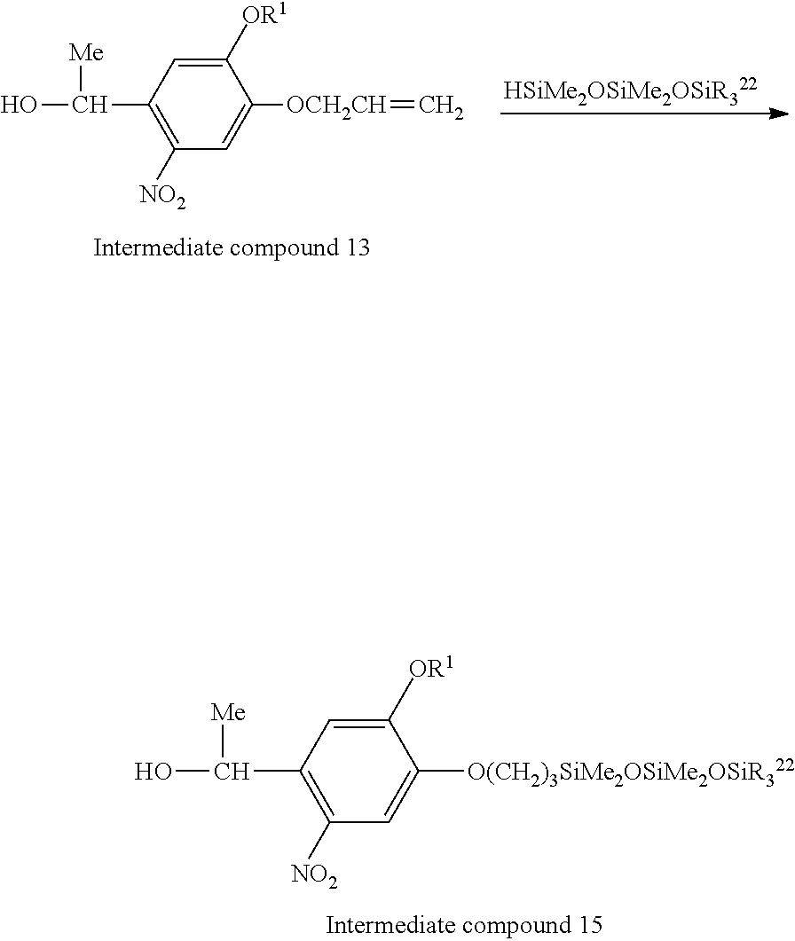


| TABLE 1 | ||
| Modifier | Irradiation with | Contact angle (° C.) |
| SiO2/Si substrate | light (15 J) | Water | Diiodomethane | 1-Bromonaphthalene |
| (MeO)3Si(CH2)3NH2 | Not available | 59.4 ± 2.9 | 36.6 ± 1.1 | 23.4 ± 1.3 |
| 1a | Before | 94.3 ± 0.3 | 58.3 ± 0.9 | 52.0 ± 0.5 |
| 1a | After | 71.4 ± 3.6 | 45.5 ± 0.7 | 37.4 ± 1.3 |
| 1b | Before | 80.2 ± 1.1 | 44.3 ± 1.4 | 36.4 ± 0.8 |
| 1b | After | 53.5 ± 1.1 | 37.5 ± 1.6 | 26.6 ± 0.5 |
| 2a | Before | 99.2 ± 0.5 | 63.2 ± 1.4 | 57.4 ± 0.8 |
| 2a | After | 62.9 ± 1.6 | 44.9 ± 1.9 | 37.7 ± 1.1 |
| 2b | Before | 92.4 ± 0.5 | 55.7 ± 1.3 | 51.1 ± 2.3 |
| 2b | After | 57.8 ± 3.1 | 42.5 ± 0.7 | 34.8 ± 0.5 |
| 2c | Before | 99.4 ± 1.0 | 65.3 ± 0.9 | 60.5 ± 1.5 |
| 2c | After (60 J) | 74.2 ± 2.9 | 48.3 ± 2.1 | 42.4 ± 3.3 |
Claims (14)


Applications Claiming Priority (4)
| Application Number | Priority Date | Filing Date | Title |
|---|---|---|---|
| JPJP2017-016229 | 2017-01-31 | ||
| JP2017016229A JP6832727B2 (en) | 2017-01-31 | 2017-01-31 | Compounds, pattern-forming substrates, photodegradable coupling agents, pattern-forming methods and transistor manufacturing methods |
| JP2017-016229 | 2017-01-31 | ||
| PCT/JP2018/002899 WO2018143173A1 (en) | 2017-01-31 | 2018-01-30 | Compound, substrate for pattern formation, photodegradable coupling agent, pattern formation method, and transistor production method |
Related Parent Applications (1)
| Application Number | Title | Priority Date | Filing Date |
|---|---|---|---|
| PCT/JP2018/002899 Continuation WO2018143173A1 (en) | 2017-01-31 | 2018-01-30 | Compound, substrate for pattern formation, photodegradable coupling agent, pattern formation method, and transistor production method |
Publications (2)
| Publication Number | Publication Date |
|---|---|
| US20190352260A1 US20190352260A1 (en) | 2019-11-21 |
| US11225461B2 true US11225461B2 (en) | 2022-01-18 |
Family
ID=63040525
Family Applications (1)
| Application Number | Title | Priority Date | Filing Date |
|---|---|---|---|
| US16/524,799 Active US11225461B2 (en) | 2017-01-31 | 2019-07-29 | Compound, substrate for pattern formation, photodegradable coupling agent, pattern formation method, and transistor production method |
Country Status (5)
| Country | Link |
|---|---|
| US (1) | US11225461B2 (en) |
| JP (1) | JP6832727B2 (en) |
| CN (1) | CN110198946B (en) |
| TW (1) | TWI767983B (en) |
| WO (1) | WO2018143173A1 (en) |
Families Citing this family (1)
| Publication number | Priority date | Publication date | Assignee | Title |
|---|---|---|---|---|
| JP7121505B2 (en) * | 2017-10-11 | 2022-08-18 | 株式会社ニコン | Compound, pattern forming substrate, photodegradable coupling agent, pattern forming method, and transistor manufacturing method |
Citations (6)
| Publication number | Priority date | Publication date | Assignee | Title |
|---|---|---|---|---|
| US20050245739A1 (en) * | 2004-04-29 | 2005-11-03 | Seiko Epson Corporation | UV decomposable molecules and a photopatternable monomolecular film formed therefrom |
| CN1715270A (en) | 2004-04-29 | 2006-01-04 | 精工爱普生株式会社 | Uv decomposable molecules and a photopatternable monomolecular film formed therefrom |
| US20060222865A1 (en) | 2003-12-04 | 2006-10-05 | Asahi Glass Company, Limited | Fluorinated compound, water repellent composition and thin film |
| JP2014145020A (en) | 2013-01-29 | 2014-08-14 | Sumitomo Chemical Co Ltd | Polymer compound, and insulating layer material including polymer compound |
| US20140240661A1 (en) * | 1998-03-02 | 2014-08-28 | Johnson & Johnson Vision Care, Inc. | Contact lenses |
| US20170285471A1 (en) * | 2015-02-25 | 2017-10-05 | Nikon Corporation | Fluorine-containing composition, substrate for pattern formation, photodegradable coupling agent, pattern formation method and transistor production method |
Family Cites Families (5)
| Publication number | Priority date | Publication date | Assignee | Title |
|---|---|---|---|---|
| JP5196287B2 (en) * | 2006-01-16 | 2013-05-15 | 学校法人神奈川大学 | Photodegradable coupling agent |
| JP2014001196A (en) * | 2011-09-12 | 2014-01-09 | Univ Kanagawa | Photodegradable coupling agent |
| WO2014038579A1 (en) * | 2012-09-04 | 2014-03-13 | 学校法人神奈川大学 | Fluorine-containing compound, substrate for pattern formation, photodegradable coupling agent, pattern formation method, and compound |
| CN105980600B (en) * | 2014-02-28 | 2019-01-18 | 株式会社尼康 | The manufacturing method of wiring pattern and the manufacturing method of transistor |
| WO2016136817A1 (en) * | 2015-02-25 | 2016-09-01 | 株式会社ニコン | Fluorine-containing composition, substrate for patterning, photo-degradable coupling agent, method for patterning, and manufacturing method for transistor |
-
2017
- 2017-01-31 JP JP2017016229A patent/JP6832727B2/en active Active
-
2018
- 2018-01-30 CN CN201880007674.0A patent/CN110198946B/en active Active
- 2018-01-30 WO PCT/JP2018/002899 patent/WO2018143173A1/en active Application Filing
- 2018-01-31 TW TW107103497A patent/TWI767983B/en active
-
2019
- 2019-07-29 US US16/524,799 patent/US11225461B2/en active Active
Patent Citations (9)
| Publication number | Priority date | Publication date | Assignee | Title |
|---|---|---|---|---|
| US20140240661A1 (en) * | 1998-03-02 | 2014-08-28 | Johnson & Johnson Vision Care, Inc. | Contact lenses |
| US20060222865A1 (en) | 2003-12-04 | 2006-10-05 | Asahi Glass Company, Limited | Fluorinated compound, water repellent composition and thin film |
| EP1736477A1 (en) | 2003-12-04 | 2006-12-27 | Asahi Glass Company, Limited | Fluorine-containing compound, water repellent composition and thin film |
| JP4997765B2 (en) | 2003-12-04 | 2012-08-08 | 旭硝子株式会社 | Fluorine-containing compound, water-repellent composition and thin film |
| US20050245739A1 (en) * | 2004-04-29 | 2005-11-03 | Seiko Epson Corporation | UV decomposable molecules and a photopatternable monomolecular film formed therefrom |
| EP1610176A2 (en) | 2004-04-29 | 2005-12-28 | Seiko Epson Corporation | UV decomposable molecules and a photopatternable monomolecular film formed therefrom |
| CN1715270A (en) | 2004-04-29 | 2006-01-04 | 精工爱普生株式会社 | Uv decomposable molecules and a photopatternable monomolecular film formed therefrom |
| JP2014145020A (en) | 2013-01-29 | 2014-08-14 | Sumitomo Chemical Co Ltd | Polymer compound, and insulating layer material including polymer compound |
| US20170285471A1 (en) * | 2015-02-25 | 2017-10-05 | Nikon Corporation | Fluorine-containing composition, substrate for pattern formation, photodegradable coupling agent, pattern formation method and transistor production method |
Non-Patent Citations (3)
| Title |
|---|
| First Office Action dated Jul. 14, 2021 in Chinese Patent Application No. 201880007674.0. |
| International Search Report dated Apr. 17, 2018 in corresponding International Patent Application No. PCT/JP2018/002899. |
| Written Opinion of the International Searching Authority dated Apr. 17, 2018 in corresponding International Patent Application No. PCT/JP2018/002899. |
Also Published As
| Publication number | Publication date |
|---|---|
| JP2018123082A (en) | 2018-08-09 |
| CN110198946A (en) | 2019-09-03 |
| TW201833124A (en) | 2018-09-16 |
| WO2018143173A1 (en) | 2018-08-09 |
| JP6832727B2 (en) | 2021-02-24 |
| TWI767983B (en) | 2022-06-21 |
| US20190352260A1 (en) | 2019-11-21 |
| CN110198946B (en) | 2022-04-26 |
Similar Documents
| Publication | Publication Date | Title |
|---|---|---|
| US11953833B2 (en) | Compound, substrate for pattern formation, photodegradable coupling agent, pattern formation method, and transistor production method | |
| US10466591B2 (en) | Fluorine-containing composition, substrate for pattern formation, photodegradable coupling agent, pattern formation method and transistor production method | |
| US11518731B2 (en) | Fluorine-containing compound, substrate for patterning, photodegradable coupling agent, patterning method, and compound | |
| US20170158606A1 (en) | Fluorine-containing compound, substrate for pattern formation, photodegradable coupling agent, pattern formation method, and compound | |
| US11225461B2 (en) | Compound, substrate for pattern formation, photodegradable coupling agent, pattern formation method, and transistor production method | |
| JP6548572B2 (en) | Pattern formation method and modification method of treated surface of object | |
| WO2016136817A1 (en) | Fluorine-containing composition, substrate for patterning, photo-degradable coupling agent, method for patterning, and manufacturing method for transistor | |
| TWI788477B (en) | Pattern forming method | |
| US20210184143A1 (en) | Transistor production method | |
| US11767327B2 (en) | Compound, pattern forming substrate, coupling agent, and pattern formation method | |
| WO2019073878A1 (en) | Compound, pattern forming substrate, photodegradable coupling agent, pattern forming method, and transistor production method | |
| JP6298989B2 (en) | Fluorine-containing compound, pattern forming substrate, photodegradable coupling agent, pattern forming method, compound, organic thin film transistor | |
| WO2020045078A1 (en) | Transistor production method | |
| WO2020100710A1 (en) | Pattern forming method, transistor manufacturing method, and film for pattern formation |
Legal Events
| Date | Code | Title | Description |
|---|---|---|---|
| FEPP | Fee payment procedure |
Free format text: ENTITY STATUS SET TO UNDISCOUNTED (ORIGINAL EVENT CODE: BIG.); ENTITY STATUS OF PATENT OWNER: LARGE ENTITY |
|
| AS | Assignment |
Owner name: KANAGAWA UNIVERSITY, JAPAN Free format text: ASSIGNMENT OF ASSIGNORS INTEREST;ASSIGNORS:KAWAKAMI, YUSUKE;YAMAGUCHI, KAZUO;ITOU, MICHIKO;SIGNING DATES FROM 20190417 TO 20190719;REEL/FRAME:049906/0362 Owner name: NIKON CORPORATION, JAPAN Free format text: ASSIGNMENT OF ASSIGNORS INTEREST;ASSIGNORS:KAWAKAMI, YUSUKE;YAMAGUCHI, KAZUO;ITOU, MICHIKO;SIGNING DATES FROM 20190417 TO 20190719;REEL/FRAME:049906/0362 |
|
| STPP | Information on status: patent application and granting procedure in general |
Free format text: APPLICATION DISPATCHED FROM PREEXAM, NOT YET DOCKETED |
|
| STPP | Information on status: patent application and granting procedure in general |
Free format text: DOCKETED NEW CASE - READY FOR EXAMINATION |
|
| STPP | Information on status: patent application and granting procedure in general |
Free format text: NON FINAL ACTION MAILED |
|
| STPP | Information on status: patent application and granting procedure in general |
Free format text: RESPONSE TO NON-FINAL OFFICE ACTION ENTERED AND FORWARDED TO EXAMINER |
|
| STPP | Information on status: patent application and granting procedure in general |
Free format text: NOTICE OF ALLOWANCE MAILED -- APPLICATION RECEIVED IN OFFICE OF PUBLICATIONS |
|
| STPP | Information on status: patent application and granting procedure in general |
Free format text: DOCKETED NEW CASE - READY FOR EXAMINATION |
|
| STPP | Information on status: patent application and granting procedure in general |
Free format text: NOTICE OF ALLOWANCE MAILED -- APPLICATION RECEIVED IN OFFICE OF PUBLICATIONS |
|
| STPP | Information on status: patent application and granting procedure in general |
Free format text: PUBLICATIONS -- ISSUE FEE PAYMENT VERIFIED |
|
| STCF | Information on status: patent grant |
Free format text: PATENTED CASE |