US11223020B2 - Flexible display panel with bent substrate - Google Patents
Flexible display panel with bent substrate Download PDFInfo
- Publication number
- US11223020B2 US11223020B2 US15/476,812 US201715476812A US11223020B2 US 11223020 B2 US11223020 B2 US 11223020B2 US 201715476812 A US201715476812 A US 201715476812A US 11223020 B2 US11223020 B2 US 11223020B2
- Authority
- US
- United States
- Prior art keywords
- layer
- flexible substrate
- display
- polymer
- adhesive
- Prior art date
- Legal status (The legal status is an assumption and is not a legal conclusion. Google has not performed a legal analysis and makes no representation as to the accuracy of the status listed.)
- Active, expires
Links
Images


Classifications
-
- H01L51/0097—
-
- H—ELECTRICITY
- H10—SEMICONDUCTOR DEVICES; ELECTRIC SOLID-STATE DEVICES NOT OTHERWISE PROVIDED FOR
- H10K—ORGANIC ELECTRIC SOLID-STATE DEVICES
- H10K59/00—Integrated devices, or assemblies of multiple devices, comprising at least one organic light-emitting element covered by group H10K50/00
- H10K59/80—Constructional details
- H10K59/87—Passivation; Containers; Encapsulations
- H10K59/873—Encapsulations
-
- G—PHYSICS
- G09—EDUCATION; CRYPTOGRAPHY; DISPLAY; ADVERTISING; SEALS
- G09F—DISPLAYING; ADVERTISING; SIGNS; LABELS OR NAME-PLATES; SEALS
- G09F9/00—Indicating arrangements for variable information in which the information is built-up on a support by selection or combination of individual elements
- G09F9/30—Indicating arrangements for variable information in which the information is built-up on a support by selection or combination of individual elements in which the desired character or characters are formed by combining individual elements
- G09F9/33—Indicating arrangements for variable information in which the information is built-up on a support by selection or combination of individual elements in which the desired character or characters are formed by combining individual elements being semiconductor devices, e.g. diodes
-
- H01L23/4985—
-
- H01L23/5387—
-
- H01L27/326—
-
- H01L27/3276—
-
- H01L51/004—
-
- H01L51/5253—
-
- H—ELECTRICITY
- H10—SEMICONDUCTOR DEVICES; ELECTRIC SOLID-STATE DEVICES NOT OTHERWISE PROVIDED FOR
- H10K—ORGANIC ELECTRIC SOLID-STATE DEVICES
- H10K59/00—Integrated devices, or assemblies of multiple devices, comprising at least one organic light-emitting element covered by group H10K50/00
- H10K59/10—OLED displays
- H10K59/12—Active-matrix OLED [AMOLED] displays
- H10K59/121—Active-matrix OLED [AMOLED] displays characterised by the geometry or disposition of pixel elements
-
- H—ELECTRICITY
- H10—SEMICONDUCTOR DEVICES; ELECTRIC SOLID-STATE DEVICES NOT OTHERWISE PROVIDED FOR
- H10K—ORGANIC ELECTRIC SOLID-STATE DEVICES
- H10K59/00—Integrated devices, or assemblies of multiple devices, comprising at least one organic light-emitting element covered by group H10K50/00
- H10K59/10—OLED displays
- H10K59/12—Active-matrix OLED [AMOLED] displays
- H10K59/122—Pixel-defining structures or layers, e.g. banks
-
- H—ELECTRICITY
- H10—SEMICONDUCTOR DEVICES; ELECTRIC SOLID-STATE DEVICES NOT OTHERWISE PROVIDED FOR
- H10K—ORGANIC ELECTRIC SOLID-STATE DEVICES
- H10K59/00—Integrated devices, or assemblies of multiple devices, comprising at least one organic light-emitting element covered by group H10K50/00
- H10K59/10—OLED displays
- H10K59/12—Active-matrix OLED [AMOLED] displays
- H10K59/131—Interconnections, e.g. wiring lines or terminals
-
- H—ELECTRICITY
- H10—SEMICONDUCTOR DEVICES; ELECTRIC SOLID-STATE DEVICES NOT OTHERWISE PROVIDED FOR
- H10K—ORGANIC ELECTRIC SOLID-STATE DEVICES
- H10K77/00—Constructional details of devices covered by this subclass and not covered by groups H10K10/80, H10K30/80, H10K50/80 or H10K59/80
- H10K77/10—Substrates, e.g. flexible substrates
- H10K77/111—Flexible substrates
-
- H—ELECTRICITY
- H10—SEMICONDUCTOR DEVICES; ELECTRIC SOLID-STATE DEVICES NOT OTHERWISE PROVIDED FOR
- H10K—ORGANIC ELECTRIC SOLID-STATE DEVICES
- H10K85/00—Organic materials used in the body or electrodes of devices covered by this subclass
- H10K85/10—Organic polymers or oligomers
- H10K85/141—Organic polymers or oligomers comprising aliphatic or olefinic chains, e.g. poly N-vinylcarbazol, PVC or PTFE
-
- H—ELECTRICITY
- H10—SEMICONDUCTOR DEVICES; ELECTRIC SOLID-STATE DEVICES NOT OTHERWISE PROVIDED FOR
- H10W—GENERIC PACKAGES, INTERCONNECTIONS, CONNECTORS OR OTHER CONSTRUCTIONAL DETAILS OF DEVICES COVERED BY CLASS H10
- H10W70/00—Package substrates; Interposers; Redistribution layers [RDL]
- H10W70/60—Insulating or insulated package substrates; Interposers; Redistribution layers
- H10W70/611—Insulating or insulated package substrates; Interposers; Redistribution layers for connecting multiple chips together
-
- H—ELECTRICITY
- H10—SEMICONDUCTOR DEVICES; ELECTRIC SOLID-STATE DEVICES NOT OTHERWISE PROVIDED FOR
- H10W—GENERIC PACKAGES, INTERCONNECTIONS, CONNECTORS OR OTHER CONSTRUCTIONAL DETAILS OF DEVICES COVERED BY CLASS H10
- H10W70/00—Package substrates; Interposers; Redistribution layers [RDL]
- H10W70/60—Insulating or insulated package substrates; Interposers; Redistribution layers
- H10W70/67—Insulating or insulated package substrates; Interposers; Redistribution layers characterised by their insulating layers or insulating parts
- H10W70/688—Flexible insulating substrates
-
- H01L2251/5338—
-
- H01L2251/558—
-
- H—ELECTRICITY
- H10—SEMICONDUCTOR DEVICES; ELECTRIC SOLID-STATE DEVICES NOT OTHERWISE PROVIDED FOR
- H10K—ORGANIC ELECTRIC SOLID-STATE DEVICES
- H10K2102/00—Constructional details relating to the organic devices covered by this subclass
- H10K2102/301—Details of OLEDs
- H10K2102/311—Flexible OLED
-
- H—ELECTRICITY
- H10—SEMICONDUCTOR DEVICES; ELECTRIC SOLID-STATE DEVICES NOT OTHERWISE PROVIDED FOR
- H10K—ORGANIC ELECTRIC SOLID-STATE DEVICES
- H10K2102/00—Constructional details relating to the organic devices covered by this subclass
- H10K2102/301—Details of OLEDs
- H10K2102/351—Thickness
-
- Y—GENERAL TAGGING OF NEW TECHNOLOGICAL DEVELOPMENTS; GENERAL TAGGING OF CROSS-SECTIONAL TECHNOLOGIES SPANNING OVER SEVERAL SECTIONS OF THE IPC; TECHNICAL SUBJECTS COVERED BY FORMER USPC CROSS-REFERENCE ART COLLECTIONS [XRACs] AND DIGESTS
- Y02—TECHNOLOGIES OR APPLICATIONS FOR MITIGATION OR ADAPTATION AGAINST CLIMATE CHANGE
- Y02E—REDUCTION OF GREENHOUSE GAS [GHG] EMISSIONS, RELATED TO ENERGY GENERATION, TRANSMISSION OR DISTRIBUTION
- Y02E10/00—Energy generation through renewable energy sources
- Y02E10/50—Photovoltaic [PV] energy
- Y02E10/549—Organic PV cells
Definitions
- This relates generally to electronic devices with displays, and, more particularly, to displays with bent portions.
- Displays such as organic light-emitting diode displays may be formed on flexible substrates. Displays with flexible substrates may be bent. For example, it may be desirable to bend an edge of a display to hide inactive display components along the edge of the display from view.
- the process of bending a display can create stresses within the structures of the display. For example, bent metal traces may become stressed. Stress-induced damage such as cracks may adversely affect display reliability.
- a display may have an array of organic light-emitting diodes that form an active area on a flexible substrate.
- Metal traces may extend between the active area and an inactive area of the flexible substrate.
- Display driver circuitry such as a display driver integrated circuit may be coupled to the inactive area.
- the metal traces may extend across a bend region in the flexible substrate. The flexible substrate may be bent in the bend region.
- the flexible substrate may be made of a thin flexible material to reduce metal trace bending stress.
- a coating layer in the bend region may be provided with an enhanced elasticity to allow its thickness to be reduced.
- the flexible substrate may be bent on itself and secured within an electronic device without using a mandrel.
- FIG. 1 is a perspective view of an illustrative electronic device having a display in accordance with an embodiment.
- FIG. 2 is a schematic diagram of an illustrative electronic device having a display in accordance with an embodiment.
- FIG. 3 is a top view of an illustrative display in an electronic device in accordance with an embodiment.
- FIG. 4 is a cross-sectional side view of a portion of an illustrative organic light-emitting diode display in accordance with an embodiment.
- FIG. 5 is perspective view of an illustrative display with a bent portion in accordance with an embodiment.
- FIG. 6 is a cross-sectional side view of an illustrative display with a bent portion in accordance with an embodiment.
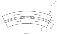
- FIG. 7 is a cross-sectional side view of an illustrative bent substrate showing how a neutral stress plane may be aligned with metal traces on the substrate using a coating layer in accordance with an embodiment.
- FIG. 8 is a cross-sectional side view of an illustrative display having a flexible substrate with a coating layer that has been bent in accordance with an embodiment.
- FIG. 9 is a cross-sectional side view of an illustrative display with a bent flexible substrate in accordance with an embodiment.
- FIGS. 10, 11, and 12 are cross-sectional side views of illustrative layers in displays with bent flexible substrates in accordance with embodiments.
- Electronic device 10 may be a computing device such as a laptop computer, a computer monitor containing an embedded computer, a tablet computer, a cellular telephone, a media player, or other handheld or portable electronic device, a smaller device such as a wrist-watch device, a pendant device, a headphone or earpiece device, a device embedded in eyeglasses or other equipment worn on a user's head, or other wearable or miniature device, a television, a computer display that does not contain an embedded computer, a gaming device, a navigation device, an embedded system such as a system in which electronic equipment with a display is mounted in a kiosk or automobile, equipment that implements the functionality of two or more of these devices, or other electronic equipment.
- a computing device such as a laptop computer, a computer monitor containing an embedded computer, a tablet computer, a cellular telephone, a media player, or other handheld or portable electronic device, a smaller device such as a wrist-watch device, a pendant device, a headphone or earpiece device, a
- device 10 is a portable device such as a cellular telephone, media player, tablet computer, wrist device, or other portable computing device. Other configurations may be used for device 10 if desired.
- FIG. 1 is merely illustrative.
- device 10 includes a display such as display 14 mounted in housing 12 .
- Housing 12 which may sometimes be referred to as an enclosure or case, may be formed of plastic, glass, ceramics, fiber composites, metal (e.g., stainless steel, aluminum, etc.), other suitable materials, or a combination of any two or more of these materials.
- Housing 12 may be formed using a unibody configuration in which some or all of housing 12 is machined or molded as a single structure or may be formed using multiple structures (e.g., an internal frame structure, one or more structures that form exterior housing surfaces, etc.).
- Display 14 may be a touch screen display that incorporates a layer of conductive capacitive touch sensor electrodes or other touch sensor components (e.g., resistive touch sensor components, acoustic touch sensor components, force-based touch sensor components, light-based touch sensor components, etc.) or may be a display that is not touch-sensitive.
- Capacitive touch screen electrodes may be formed from an array of indium tin oxide pads or other transparent conductive structures.
- Display 14 may include an array of display pixels formed from liquid crystal display (LCD) components, an array of electrophoretic display pixels, an array of plasma display pixels, microelectromechanical (MEMs) shutter pixels, electrowetting pixels, micro-light-emitting diodes (small crystalline semiconductor die), organic light-emitting diodes (e.g., a thin-film organic light-emitting diode display), quantum dot light-emitting diodes, or display pixels based on other display technologies.
- the array of display pixels may display images for a user in active area of display 14 .
- the active area may be surrounded on one or more sides by inactive border regions.
- Display 14 may be protected using a display cover layer such as a layer of transparent glass or clear plastic. Openings may be formed in the display cover layer. For example, an opening may be formed in the display cover layer to accommodate a button, a speaker port, or other component. Openings may be formed in housing 12 to form communications ports (e.g., an audio jack port, a digital data port, etc.), to form openings for buttons, etc.
- a display cover layer such as a layer of transparent glass or clear plastic.
- Openings may be formed in the display cover layer.
- an opening may be formed in the display cover layer to accommodate a button, a speaker port, or other component.
- Openings may be formed in housing 12 to form communications ports (e.g., an audio jack port, a digital data port, etc.), to form openings for buttons, etc.
- FIG. 2 is a schematic diagram of device 10 .
- electronic device 10 may have control circuitry 16 .
- Control circuitry 16 may include storage and processing circuitry for supporting the operation of device 10 .
- the storage and processing circuitry may include storage such as hard disk drive storage, nonvolatile memory (e.g., flash memory or other electrically-programmable-read-only memory configured to form a solid state drive), volatile memory (e.g., static or dynamic random-access-memory), etc.
- Processing circuitry in control circuitry 16 may be used to control the operation of device 10 .
- the processing circuitry may be based on one or more microprocessors, microcontrollers, digital signal processors, baseband processors, power management units, audio chips, application specific integrated circuits, etc.
- Input-output circuitry in device 10 such as input-output devices 18 may be used to allow data to be supplied to device 10 and to allow data to be provided from device 10 to external devices.
- Input-output devices 18 may include buttons, joysticks, scrolling wheels, touch pads, key pads, keyboards, microphones, speakers, tone generators, vibrators, cameras, sensors, light-emitting diodes and other status indicators, data ports, etc.
- a user can control the operation of device 10 by supplying commands through input-output devices 18 and may receive status information and other output from device 10 using the output resources of input-output devices 18 .
- Input-output devices 18 may include one or more displays such as display 14 .
- Control circuitry 16 may be used to run software on device 10 such as operating system code and applications. During operation of device 10 , the software running on control circuitry 16 may display images on display 14 using an array of pixels in display 14 .
- Display 14 may have a rectangular shape (i.e., display 14 may have a rectangular footprint and a rectangular peripheral edge that runs around the rectangular footprint) or may have other suitable shapes. Display 14 may be planar or may have a curved profile.
- FIG. 3 A top view of a portion of display 14 is shown in FIG. 3 .
- display 14 may have an array of pixels 22 .
- Pixels 22 may receive data signals over signal paths such as data lines D and may receive one or more control signals over control signal paths such as horizontal control lines G (sometimes referred to as gate lines, scan lines, emission control lines, etc.).
- horizontal control lines G sometimes referred to as gate lines, scan lines, emission control lines, etc.
- Each pixel 22 may have a light-emitting diode 26 that emits light 24 under the control of a pixel control circuit formed from thin-film transistor circuitry such as thin-film transistors 28 and thin-film capacitors).
- Thin-film transistors 28 may be polysilicon thin-film transistors, semiconducting-oxide thin-film transistors such as indium zinc gallium oxide transistors, or thin-film transistor
- FIG. 4 A cross-sectional side view of a portion of an illustrative organic light-emitting diode display in the vicinity of one of light-emitting diodes 26 is shown in FIG. 4 .
- display 14 may include a substrate layer such as substrate layer 30 .
- Substrate 30 may be formed from plastic or other suitable materials. Configurations for display 14 in which substrate 30 has been formed from a flexible material such as polyimide or other flexible polymer are sometimes described herein as an example.
- Thin-film transistor circuitry 44 may be formed on substrate 30 .
- Thin film transistor circuitry 44 may include layers 32 .
- Layers 32 may include inorganic layers such as inorganic buffer layers, gate insulator, passivation, interlayer dielectric, and other inorganic dielectric layers.
- Layers 32 may also include organic dielectric layers such as a polymer planarization layer.
- Metal layers and semiconductor layers may also be included within layers 32 .
- semiconductors such as silicon, semiconducting-oxide semiconductors, or other semiconductor materials may be used in forming semiconductor channel regions for thin-film transistors 28 .
- Metal in layers 32 may be used in forming transistor gate terminals, transistor source-drain terminals, capacitor electrodes, and metal interconnects.
- thin-film transistor circuitry 44 may include diode anode structures such as anode 36 .
- Anode 36 may be formed from a layer of conductive material such as metal on the surface of layers 32 (e.g., on the surface of a planarization layer that covers underlying thin-film transistor structures).
- Light-emitting diode 26 may be formed within an opening in pixel definition layer 40 .
- Pixel definition layer 40 may be formed from a patterned photoimageable polymer such as polyimide.
- organic emissive material 38 is interposed between a respective anode 36 and cathode 42 .
- Anodes 36 may be patterned from a layer of metal.
- Cathode 42 may be formed from a common conductive layer that is deposited on top of pixel definition layer 40 . Cathode 42 is transparent so that light 24 may exit light emitting diode 26 . During operation, light-emitting diode 26 may emit light 24 .
- Metal interconnect structures may be used to interconnect transistors and other components in circuitry 44 .
- Metal interconnect lines may also be used to route signals to capacitors, to data lines D and gate lines G, to contact pads (e.g., contact pads coupled to gate driver circuitry), and to other circuitry in display 14 .
- layers 32 may include one or more layers of patterned metal for forming interconnects such as metal traces 74 .
- display 14 may have a protective outer display layer such as cover glass layer 70 .
- the outer display layer may be formed from a material such as sapphire, glass, plastic, clear ceramic, or other transparent material.
- Protective layer 46 may cover cathode 42 .
- Layer 46 may include moisture barrier structures, encapsulant materials, adhesive, and/or other materials to help protect thin-film transistor circuitry.
- Functional layers 68 may be interposed between layer 46 and cover layer 70 .
- Functional layers 68 may include a touch sensor layer, a circular polarizer layer, and other layers.
- a circular polarizer layer may help reduce light reflections from metal traces in thin-film transistor circuitry 44 .
- a touch sensor layer may be formed from an array of capacitive touch sensor electrodes on a flexible polymer substrate.
- the touch sensor layer may be used to gather touch input from the fingers of a user, from a stylus, or from other external objects.
- Layers of optically clear adhesive may be used to attach cover glass layer 70 and functional layers 68 to underlying display layers such as layer 46 , thin-film transistor circuitry 44 , and substrate 30 .
- Display 14 may have an active area in which pixels 22 form images for viewing by a user of device 10 .
- the active area may have a rectangular shape.
- Inactive portions of display 14 may surround the active area.
- signal traces and other support circuitry such as thin-film display driver circuitry may be formed along one or more of the four edges of display 14 that run around the rectangular periphery of display 14 adjacent to the active area.
- one or more display driver integrated circuits may be mounted to substrate 30 in the inactive border.
- a flexible printed circuit on which one or more display driver integrated circuits have been mounted using solder may be attached to the border of display 14 . This type of configuration is sometimes referred to as a chip-on-flex configuration and allows display driver circuitry to supply signals to the data and gate lines on display 14 .
- one or more edges of display 14 may be bent.
- the edge of display 14 to which a display driver circuit is mounted using a chip-on-flex arrangement may be folded under the active area of display 14 . This helps minimize visible display borders and reduces the footprint of display 14 .
- FIG. 5 An illustrative display with a bent edge portion is shown in FIG. 5 .
- display 14 has portion 14 A (i.e., a planar active area portion that contains the active area of display 14 that is formed by an array of pixels 22 ), bent portion 14 B, and inactive portion 14 C.
- portion 14 A i.e., a planar active area portion that contains the active area of display 14 that is formed by an array of pixels 22
- bent portion 14 B i.e., a planar active area portion that contains the active area of display 14 that is formed by an array of pixels 22
- bent portion 14 B i.e., a planar active area portion that contains the active area of display 14 that is formed by an array of pixels 22
- inactive portion 14 C i.e., a planar active area portion that contains the active area of display 14 that is formed by an array of pixels 22
- inactive portion 14 C i.e., a planar active area portion that contains the active area of display 14 that is formed by an array
- Metal traces 74 may carry signals between inactive area 14 C of display 14 and active area 14 A of display 14 (i.e., metal traces 74 may traverse bent portion 14 B of display 14 ). As shown in the cross-sectional side view of the illustrative display of FIG. 6 , when bent portion 14 B is bent around bend axis 72 , portion 14 C is folded under portion 14 A and is therefore hidden from view by a user such as viewer 80 who is viewing display 14 in direction 82 . As shown in FIG. 6 , components 76 (e.g., display driver circuitry, etc.) may be mounted on the upper and/or lower surface of display 14 in region 14 C.
- components 76 e.g., display driver circuitry, etc.
- An optional support structure such as mandrel 78 may be used to support display 14 in bend region 14 B (e.g., to help establish a desired minimum bend radius in region 14 B) or, more preferably, mandrel 78 may be omitted to help minimize display thickness (e.g., by allowing portions 14 A and 14 C to be mounted more closely together and by allowing the bend radius for region 14 B to be reduced).
- metal traces such as metal traces 74 of FIG. 5 that are used to form signal lines that convey signals between display driver circuitry or other circuits in inactive region 14 C and pixels 22 in region 14 A may be subjected to bending stresses in bend region 14 B.
- metal traces 74 it may be desirable to align the neutral stress plane of display 14 in bend region 14 B with metal traces 74 .
- neutral stress plane 86 arises where stress has been eliminated by balancing the compressive stress and tensile stress.
- the shape of neutral stress plane 86 may be curved in a curved portion of display 14 such as portion 14 B of FIG. 7 (i.e., neutral stress plane 86 may have a curved profile).
- the relative thicknesses of substrate 30 and coating 84 and the relative modulus of elasticity values for substrate 30 and coating 84 determine the location of the neutral stress plane within the layers of bent display region 14 B. For example, if the elasticity of substrate 30 and coating 84 is the same, neutral stress plane 86 can be aligned with metal traces 74 by ensuring that coating 84 has the same thickness as substrate 30 . If, on the other hand, coating 84 has an elasticity that is larger than that of substrate 30 , coating 84 need not be as thick as substrate 30 to balance the compressive and tensile stresses.
- FIG. 8 shows how coating 84 may be characterized by a thickness TB and elasticity E 2 and how substrate 30 may be characterized by a thickness TA and elasticity E 1 .
- the elasticity values E 1 and E 2 and the thickness values TA and TB may be selected to help ensure that region 14 B does not impart undesired stress to metal traces 74 .
- thickness TA may be minimized (e.g., TA may be less than 16 microns, may be 5-15 microns, may be 8 microns, may be 6-12 microns, may be more than 5 microns, etc.) and substrate elasticity E 1 may be minimized (e.g., E 1 may be less than 9 GPa, may be less than 7 GPa, may be less than 5 GPa, may be 2-3 GPa, may be 1-5 GPa, or may be more than 0.5 GPa) to make flexible substrate 30 more flexible than would otherwise be possible.
- E 1 may be less than 9 GPa, may be less than 7 GPa, may be less than 5 GPa, may be 2-3 GPa, may be 1-5 GPa, or may be more than 0.5 GPa
- the thickness TB and elasticity E 2 of coating 84 may be selected to balance the compressive stress produced when bending substrate 30 . With one suitable arrangement, the elasticity E 2 may be enhanced to help minimize the magnitude of thickness T 2 (and therefore reduce display thickness).
- the value of E 2 may be, for example, about 1 GPa, 0.7 to 1.3 GPa, more than 0.5 GPa, more than 0.7 GPa, more than 0.8 GPa, or less than 2 GPa (as examples).
- Substrate 30 may be, for example, polyimide and coating 84 may be, for example, a polymer adhesive that is thermally cured or that is cured by application of ultraviolet light.
- FIG. 9 is a cross-sectional side view of an illustrative arrangement that may be used for bending display 14 (e.g., when it is desired to omit mandrel 78 of FIG. 6 ).
- display 14 may have active portion 14 A, bent portion 14 B, and inactive portion 14 C.
- moisture barrier film 90 may cover the array of organic light-emitting diode pixels 22 and other thin-film transistor circuitry 44 to prevent moisture damage.
- Layers 68 may be interposed between cover layer 70 and moisture barrier layer 90 .
- Layers 68 may include polarizer 68 A (which may be attached to film 90 with pressure sensitive adhesive), optically clear adhesive layer 68 B, touch sensor 68 C, and optically clear adhesive 68 D (as an example).
- coating 84 may be used to adjust the location of the neutral stress plane in display 14 to avoid damage to metal traces 74 .
- Portion 14 C may be bent under portion 14 A and may be secured to the underside of portion 14 A using layers such as layers 92 and 98 .
- Layer 92 may include a polymer layer such as polymer substrate layer 94 and a pressure sensitive adhesive layer such as layer 96 that attaches layer 94 to substrate 30 .
- Layer 98 may include a polymer layer such a polymer substrate 102 and a pressure sensitive adhesive layer such as layer 100 that attaches layer 102 to substrate 30 .
- Adhesive layer 96 may be interposed between layers 92 and 98 and may attach layer 94 to layer 102 , thereby attaching the folded portion of display 14 to itself.
- Layer 96 may be a foam adhesive, a layer of pressure sensitive adhesive, or other suitable adhesive.
- the thickness of layer 96 may be 30-250 microns, more than 25 microns, or less than 300 microns.
- the thickness of substrates 94 and 102 may be 100 microns, more than 50 microns, less than 150 microns, 70-130 microns, etc.
- the thickness of adhesive layers 96 and 100 may be 25 microns, more than 10 microns, less than 50 microns, etc.
- display thickness can be minimized by allowing the display to be folded over against itself and attached together with adhesive (i.e., by allowing portion 14 C to be folded and secured against portion 14 A without use of a mandrel).
- FIGS. 10, 11, and 12 are cross-sectional side views of additional configurations for the layers in displays with bent flexible substrates.
- layer 92 does not extend outwards as far as layer 98 , so ledge portion 98 L of layer 98 is exposed and the edges of layers 92 and 98 at the bent portion for display 14 are not aligned with each other.
- Arrangements of the type shown in FIG. 10 may help bend portion 14 B of display 14 with a desired bend profile.
- edges of layers 98 and 92 i.e., respective edge surfaces 98 E and 92 E
- edge surface (edge) 104 E of adhesive layer 104 As with the arrangements of FIGS. 9 and 10 , the use of this arrangement for layers 98 and 92 may be helpful in adjusting display 14 so that portion 14 B exhibits a desired bend profile.
- edge 104 E of adhesive layer 104 may extend outwardly towards bent portion 14 B of display 14 past edges 92 E and 98 E of layers 92 and 98 .
- This type of arrangement is shown in FIG. 12 .
- adhesive layer 104 may protrude sufficiently far past edges 92 E and 98 E that edge surface 104 E of layer 104 contacts and supports inner surface 301 of substrate 30 .
- the use of a protruding adhesive layer such as layer 104 of FIG. 12 may help ensure that bent display portion 14 B exhibits a desired bend profile.
- substrate 30 may be used to form any suitable devices.
- circuitry may be formed on substrate 30 in regions 14 A, 14 B, and/or 14 C that forms one or more touch sensors that are free of pixels (i.e., pixels 22 may be replaced by touch sensor electrodes, packaged sensors, or other sensor structures), that forms force sensors, or that forms other electrical components with or without including pixels on substrate 30 .
- Thin-film circuitry and/or circuitry that forms part of a discrete device may be formed on substrate 30 (e.g., in regions 14 A, 14 B, and/or 14 C) and may include sensors, integrated circuits with sensor circuitry or other sensor structures, input-output circuitry, control circuitry, or other circuitry.
- the circuitry on substrate 30 may allow some or all of substrate 30 to serve as a signal cable (e.g., a flexible printed circuit cable that contains signal lines for routing signals between different portions of device 10 ).
- metal traces may extend across bent region 14 B to allow signal to pass between circuitry in regions 14 A and 14 C and, if desired, to route signals to and from circuitry in regions 14 B.
- the use of a portion of substrate 30 in forming a display is merely illustrative.
Landscapes
- Engineering & Computer Science (AREA)
- Microelectronics & Electronic Packaging (AREA)
- Physics & Mathematics (AREA)
- Geometry (AREA)
- Devices For Indicating Variable Information By Combining Individual Elements (AREA)
- Chemical & Material Sciences (AREA)
- Materials Engineering (AREA)
- General Physics & Mathematics (AREA)
- Theoretical Computer Science (AREA)
- Electroluminescent Light Sources (AREA)
Abstract
Description
Claims (18)
Priority Applications (1)
| Application Number | Priority Date | Filing Date | Title |
|---|---|---|---|
| US15/476,812 US11223020B2 (en) | 2015-01-12 | 2017-03-31 | Flexible display panel with bent substrate |
Applications Claiming Priority (3)
| Application Number | Priority Date | Filing Date | Title |
|---|---|---|---|
| US201562102284P | 2015-01-12 | 2015-01-12 | |
| US14/987,129 US9614168B2 (en) | 2015-01-12 | 2016-01-04 | Flexible display panel with bent substrate |
| US15/476,812 US11223020B2 (en) | 2015-01-12 | 2017-03-31 | Flexible display panel with bent substrate |
Related Parent Applications (1)
| Application Number | Title | Priority Date | Filing Date |
|---|---|---|---|
| US14/987,129 Continuation US9614168B2 (en) | 2015-01-12 | 2016-01-04 | Flexible display panel with bent substrate |
Publications (2)
| Publication Number | Publication Date |
|---|---|
| US20170263873A1 US20170263873A1 (en) | 2017-09-14 |
| US11223020B2 true US11223020B2 (en) | 2022-01-11 |
Family
ID=56368141
Family Applications (2)
| Application Number | Title | Priority Date | Filing Date |
|---|---|---|---|
| US14/987,129 Active US9614168B2 (en) | 2015-01-12 | 2016-01-04 | Flexible display panel with bent substrate |
| US15/476,812 Active 2036-09-16 US11223020B2 (en) | 2015-01-12 | 2017-03-31 | Flexible display panel with bent substrate |
Family Applications Before (1)
| Application Number | Title | Priority Date | Filing Date |
|---|---|---|---|
| US14/987,129 Active US9614168B2 (en) | 2015-01-12 | 2016-01-04 | Flexible display panel with bent substrate |
Country Status (6)
| Country | Link |
|---|---|
| US (2) | US9614168B2 (en) |
| EP (2) | EP3245678B1 (en) |
| KR (2) | KR101950128B1 (en) |
| CN (3) | CN205680685U (en) |
| TW (1) | TWI625846B (en) |
| WO (1) | WO2016114996A1 (en) |
Cited By (2)
| Publication number | Priority date | Publication date | Assignee | Title |
|---|---|---|---|---|
| US20210280826A1 (en) * | 2020-03-05 | 2021-09-09 | Samsung Display Co., Ltd. | Display device |
| US12262583B2 (en) | 2018-10-11 | 2025-03-25 | Samsung Display Co., Ltd. | Display device and manufacturing method thereof |
Families Citing this family (112)
| Publication number | Priority date | Publication date | Assignee | Title |
|---|---|---|---|---|
| US9614168B2 (en) | 2015-01-12 | 2017-04-04 | Apple Inc. | Flexible display panel with bent substrate |
| KR102312314B1 (en) * | 2015-01-28 | 2021-10-13 | 삼성디스플레이 주식회사 | Touch sensor device and manufacturing method |
| US9933870B2 (en) * | 2015-03-17 | 2018-04-03 | Lg Display Co., Ltd. | Back plate member for flexible display, display apparatus including the same, and method of manufacturing the same |
| KR20160126155A (en) * | 2015-04-22 | 2016-11-02 | 삼성디스플레이 주식회사 | Flexible display panel and method of manufacturing thereof |
| KR102322084B1 (en) * | 2015-04-30 | 2021-11-04 | 삼성디스플레이 주식회사 | Touch sensor device and manufacturing method |
| JP6474337B2 (en) * | 2015-08-27 | 2019-02-27 | 株式会社ジャパンディスプレイ | Display device and manufacturing method thereof |
| JP6727843B2 (en) | 2016-02-25 | 2020-07-22 | 株式会社ジャパンディスプレイ | Display device |
| JP6378706B2 (en) * | 2016-02-26 | 2018-08-22 | 株式会社ジャパンディスプレイ | Display device manufacturing method and display device |
| KR102504128B1 (en) * | 2016-03-11 | 2023-02-28 | 삼성디스플레이 주식회사 | Flexible display device |
| JP6695727B2 (en) * | 2016-04-08 | 2020-05-20 | 株式会社ジャパンディスプレイ | Display device |
| KR102569928B1 (en) * | 2016-05-18 | 2023-08-24 | 삼성디스플레이 주식회사 | Flexible Display |
| KR102696595B1 (en) * | 2016-07-27 | 2024-08-22 | 삼성디스플레이 주식회사 | Window for display device and flexible display device including the same |
| US10643511B2 (en) * | 2016-08-19 | 2020-05-05 | Apple Inc. | Electronic device display with monitoring circuitry |
| KR102474030B1 (en) * | 2016-08-23 | 2022-12-06 | 삼성전자주식회사 | Flexible Display Apparatus and Manufacturing Method of Flexible Display Apparatus |
| US20180090720A1 (en) * | 2016-09-27 | 2018-03-29 | Universal Display Corporation | Flexible OLED Display Module |
| JP2018078057A (en) * | 2016-11-11 | 2018-05-17 | 株式会社ジャパンディスプレイ | Display device |
| JP2018109683A (en) * | 2016-12-28 | 2018-07-12 | 株式会社ジャパンディスプレイ | Display device |
| CN108281428A (en) * | 2017-01-06 | 2018-07-13 | 昆山工研院新型平板显示技术中心有限公司 | A kind of metal wire and flexible display panels |
| WO2018129148A1 (en) * | 2017-01-06 | 2018-07-12 | Carestream Health, Inc. | Detach and reattach of a flexible polyimide based x-ray detector |
| TWI624938B (en) * | 2017-03-28 | 2018-05-21 | 友達光電股份有限公司 | Micro light emitting diode display device |
| CN106910823B (en) * | 2017-04-05 | 2019-08-06 | 上海天马微电子有限公司 | A kind of flexible display panel and flexible display device |
| CN107146527B (en) | 2017-04-27 | 2020-01-03 | 上海天马微电子有限公司 | Flexible display screen and flexible display device |
| CN110612605B (en) * | 2017-05-15 | 2023-05-30 | 卡尔斯特里姆保健公司 | Digital radiography image sensor |
| JP2019012098A (en) * | 2017-06-29 | 2019-01-24 | 株式会社ジャパンディスプレイ | Display device |
| US10649267B2 (en) * | 2017-07-19 | 2020-05-12 | Innolux Corporation | Display device and manufacturing method thereof |
| TWI627777B (en) * | 2017-07-26 | 2018-06-21 | 財團法人工業技術研究院 | Optical compensation structure |
| KR20190014273A (en) | 2017-07-31 | 2019-02-12 | 삼성디스플레이 주식회사 | Display apparatus and manufacturing method of the same |
| KR102340729B1 (en) | 2017-07-31 | 2021-12-16 | 엘지디스플레이 주식회사 | Organic light emitting display device |
| KR102336569B1 (en) * | 2017-07-31 | 2021-12-06 | 엘지디스플레이 주식회사 | Display apparatus and multi screen display apparatus comprising the same |
| KR102517092B1 (en) * | 2017-08-02 | 2023-04-04 | 삼성전자주식회사 | An electronic device comprising a flexible display panel |
| US20190051707A1 (en) * | 2017-08-14 | 2019-02-14 | Wuhan China Star Optoelectronics Semiconductor Display Technology Co., Ltd. | Oled touch display panel and oled touch display |
| US10721825B2 (en) | 2017-08-18 | 2020-07-21 | Google Llc | Bent display panel with electrical lines for a sensor |
| KR102411537B1 (en) | 2017-09-06 | 2022-06-22 | 삼성디스플레이 주식회사 | Method of manufacturing display apparatus and display apparatus |
| KR102423192B1 (en) | 2017-09-06 | 2022-07-21 | 삼성디스플레이 주식회사 | Foldable display apparatus and the manufacturing method thereof |
| US10775490B2 (en) * | 2017-10-12 | 2020-09-15 | Infineon Technologies Ag | Radio frequency systems integrated with displays and methods of formation thereof |
| TW202326261A (en) * | 2017-10-16 | 2023-07-01 | 美商康寧公司 | Bezel-free display tile with edge-wrapped conductors and methods of manufacture |
| KR102508668B1 (en) | 2017-11-24 | 2023-03-13 | 삼성디스플레이 주식회사 | Display apparatus and method of manufacturing the same |
| KR102452529B1 (en) * | 2017-12-12 | 2022-10-11 | 삼성디스플레이 주식회사 | Flexible substrate and display device including the same |
| CN108172127A (en) * | 2017-12-15 | 2018-06-15 | 武汉华星光电半导体显示技术有限公司 | Flexible display panels |
| KR102020824B1 (en) * | 2017-12-22 | 2019-10-18 | 엘지디스플레이 주식회사 | Flexible Electroluminescent Display Device |
| US10910592B2 (en) | 2017-12-22 | 2021-02-02 | Lg Display Co., Ltd. | Flexible electroluminescent display device |
| US20210076504A1 (en) * | 2017-12-22 | 2021-03-11 | Molex, Llc | Double-sided assembly on flexible substrates |
| US11506363B2 (en) * | 2018-01-09 | 2022-11-22 | OLEDWorks LLC | Ultrathin OLED lighting panel |
| KR102518132B1 (en) | 2018-02-14 | 2023-04-06 | 삼성디스플레이 주식회사 | Display device |
| KR102451778B1 (en) | 2018-02-20 | 2022-10-06 | 삼성디스플레이 주식회사 | Display device |
| KR102481384B1 (en) * | 2018-03-08 | 2022-12-27 | 삼성디스플레이 주식회사 | Foldable display apparatus and the manufacturing method thereof |
| KR102455037B1 (en) | 2018-03-08 | 2022-10-17 | 삼성디스플레이 주식회사 | Foldable display apparatus and the manufacturing method thereof |
| KR102322697B1 (en) | 2018-03-08 | 2021-11-08 | 삼성전자주식회사 | Flexible display and electronic device having the same |
| CN108493212A (en) * | 2018-03-13 | 2018-09-04 | 武汉华星光电半导体显示技术有限公司 | Flexible Displays structure and electronic equipment |
| KR102562373B1 (en) | 2018-05-31 | 2023-08-02 | 삼성디스플레이 주식회사 | Display apparatus and manufacturing method of the same |
| US11054861B2 (en) | 2018-06-11 | 2021-07-06 | Apple Inc. | Electronic devices having displays with expanded edges |
| KR102662203B1 (en) | 2018-07-17 | 2024-04-30 | 삼성디스플레이 주식회사 | Display device |
| CN108962031B (en) * | 2018-07-24 | 2022-02-08 | 上海天马微电子有限公司 | Display panel and display device |
| US11099439B2 (en) | 2018-09-11 | 2021-08-24 | Apple Inc. | Display device assembly having a spacer layer surrounding the integrated circuit |
| KR102568726B1 (en) | 2018-09-18 | 2023-08-22 | 삼성디스플레이 주식회사 | Display device |
| KR102617925B1 (en) | 2018-09-27 | 2023-12-26 | 삼성디스플레이 주식회사 | Display device |
| KR102670077B1 (en) | 2018-10-05 | 2024-05-28 | 삼성디스플레이 주식회사 | Display device and manufacturing method therof |
| CN111048549B (en) * | 2018-10-11 | 2022-08-16 | 上海和辉光电股份有限公司 | Display panel, display device and preparation method of display panel |
| KR102562604B1 (en) * | 2018-11-08 | 2023-08-01 | 엘지디스플레이 주식회사 | Flexible Electroluminescent Display Apparatus |
| KR102656855B1 (en) * | 2018-11-15 | 2024-04-11 | 엘지디스플레이 주식회사 | Flexible Electroluminescent Display Apparatus |
| US11296063B2 (en) * | 2018-11-20 | 2022-04-05 | Lumens Co., Ltd. | Flexible LED display with processor under a folded edge portion |
| USD920440S1 (en) | 2018-12-04 | 2021-05-25 | Aristocrat Technologies Australia Pty Limited | Curved button panel display for an electronic gaming machine |
| US10741009B2 (en) | 2018-12-04 | 2020-08-11 | Aristocrat Technologies Australia Pty Limited | Curved button deck display |
| USD920439S1 (en) | 2018-12-04 | 2021-05-25 | Aristocrat Technologies Australia Pty Limited | Curved button panel display for an electronic gaming machine |
| USD920441S1 (en) | 2018-12-04 | 2021-05-25 | Aristocrat Technologies Australia Pty Limited | Curved button panel display for an electronic gaming machine |
| USD923592S1 (en) * | 2018-12-18 | 2021-06-29 | Aristocrat Technologies Australia Pty Limited | Electronic gaming machine |
| US10733830B2 (en) | 2018-12-18 | 2020-08-04 | Aristocrat Technologies Pty Limited | Gaming machine display having one or more curved edges |
| US11853515B2 (en) | 2018-12-19 | 2023-12-26 | Apple Inc. | Ultra-thin touch sensors |
| DE102019219598A1 (en) | 2018-12-19 | 2020-06-25 | Apple Inc. | ULTRA-THIN TOUCH SENSORS |
| US11067884B2 (en) * | 2018-12-26 | 2021-07-20 | Apple Inc. | Through-display optical transmission, reception, or sensing through micro-optic elements |
| KR102563626B1 (en) | 2019-01-09 | 2023-08-04 | 삼성전자 주식회사 | Flexible display and electronic device including the same |
| CN109830182A (en) | 2019-01-25 | 2019-05-31 | 武汉华星光电半导体显示技术有限公司 | Flexible display |
| CN109686776B (en) * | 2019-01-29 | 2020-11-24 | 武汉华星光电半导体显示技术有限公司 | Display panel and display device |
| KR102794534B1 (en) | 2019-03-11 | 2025-04-10 | 삼성디스플레이 주식회사 | display apparatus type bending device |
| US10838556B2 (en) | 2019-04-05 | 2020-11-17 | Apple Inc. | Sensing system for detection of light incident to a light emitting layer of an electronic device display |
| KR102840571B1 (en) | 2019-05-09 | 2025-07-30 | 삼성디스플레이 주식회사 | Display device |
| WO2020232377A1 (en) * | 2019-05-15 | 2020-11-19 | Thermal Corp. | Vapor chamber thermal strap assembly and method |
| KR20200138529A (en) * | 2019-05-30 | 2020-12-10 | 삼성디스플레이 주식회사 | Display device |
| EP3785897B1 (en) | 2019-08-29 | 2021-12-29 | SHPP Global Technologies B.V. | Transparent, flexible, impact resistant, multilayer film comprising polycarbonate copolymers |
| US11527582B1 (en) | 2019-09-24 | 2022-12-13 | Apple Inc. | Display stack with integrated photodetectors |
| US11611058B2 (en) | 2019-09-24 | 2023-03-21 | Apple Inc. | Devices and systems for under display image sensor |
| US12353241B1 (en) * | 2019-09-25 | 2025-07-08 | Apple Inc. | Electronic devices with display support structures |
| US11050030B2 (en) * | 2019-09-25 | 2021-06-29 | Wuhan China Star Optoelectronics Semiconductor Display Technology Co., Ltd. | OLED display and OLED display device |
| KR102821257B1 (en) * | 2019-10-14 | 2025-06-17 | 코닝 인코포레이티드 | Foldable device and its manufacturing method |
| CN210489620U (en) * | 2019-12-02 | 2020-05-08 | 京东方科技集团股份有限公司 | Display substrate and display device |
| KR102919916B1 (en) | 2019-12-10 | 2026-01-29 | 삼성디스플레이 주식회사 | Display device and method of manufacturing for display device |
| CN111129086B (en) * | 2019-12-13 | 2024-06-18 | 武汉华星光电技术有限公司 | Flexible display panel and manufacturing method thereof |
| KR102131372B1 (en) * | 2020-01-10 | 2020-07-09 | 삼성디스플레이 주식회사 | Display device |
| US11417848B2 (en) | 2020-01-29 | 2022-08-16 | Samsung Display Co., Ltd. | Foldable display device |
| KR102923874B1 (en) | 2020-02-11 | 2026-02-09 | 삼성디스플레이 주식회사 | Display device |
| US11592873B2 (en) | 2020-02-14 | 2023-02-28 | Apple Inc. | Display stack topologies for under-display optical transceivers |
| US11295664B2 (en) | 2020-03-11 | 2022-04-05 | Apple Inc. | Display-synchronized optical emitters and transceivers |
| US11327237B2 (en) | 2020-06-18 | 2022-05-10 | Apple Inc. | Display-adjacent optical emission or reception using optical fibers |
| US12079036B2 (en) * | 2020-06-25 | 2024-09-03 | Apple Inc. | Electronic devices with molded display mounting structures |
| US11487859B2 (en) | 2020-07-31 | 2022-11-01 | Apple Inc. | Behind display polarized optical transceiver |
| US11940848B2 (en) * | 2020-08-14 | 2024-03-26 | Apple Inc. | Electronic devices with borderless displays |
| US11889647B2 (en) * | 2020-08-19 | 2024-01-30 | Apple Inc. | Display panel bend reinforcement |
| US11961946B2 (en) * | 2020-09-10 | 2024-04-16 | Apple Inc. | Electronic devices with flexible displays |
| KR102874057B1 (en) * | 2020-11-27 | 2025-10-22 | 후아웨이 테크놀러지 컴퍼니 리미티드 | Screen covers, display devices, and electronic devices |
| US12204717B2 (en) | 2020-12-09 | 2025-01-21 | Apple Inc. | Systems and methods for flex circuit connections in touch screens |
| KR20220115647A (en) | 2021-02-08 | 2022-08-18 | 삼성디스플레이 주식회사 | Display device and electronic device having the same |
| US12003657B2 (en) * | 2021-03-02 | 2024-06-04 | Apple Inc. | Handheld electronic device |
| US11839133B2 (en) | 2021-03-12 | 2023-12-05 | Apple Inc. | Organic photodetectors for in-cell optical sensing |
| CN115273655B (en) * | 2021-04-30 | 2025-03-21 | 京东方科技集团股份有限公司 | Foldable display device |
| KR102890701B1 (en) * | 2021-07-15 | 2025-11-25 | 삼성디스플레이 주식회사 | Display device |
| KR20230019296A (en) | 2021-07-29 | 2023-02-08 | 삼성디스플레이 주식회사 | Display device |
| US12124002B2 (en) | 2021-09-03 | 2024-10-22 | Apple Inc. | Beam deflector metasurface |
| KR20230039852A (en) | 2021-09-14 | 2023-03-22 | 삼성디스플레이 주식회사 | Display device |
| KR102890699B1 (en) | 2021-09-23 | 2025-11-25 | 삼성디스플레이 주식회사 | Display device and manufacturing method of the same |
| KR20240038214A (en) | 2022-09-15 | 2024-03-25 | 삼성디스플레이 주식회사 | Display apparatus and manufacturing methode thereof |
| KR20240080307A (en) * | 2022-11-29 | 2024-06-07 | 삼성디스플레이 주식회사 | Display appratus and method for manufacturing display apparatus |
| US20240219975A1 (en) * | 2022-12-28 | 2024-07-04 | Lg Electronics Inc. | Portable electronic device |
Citations (77)
| Publication number | Priority date | Publication date | Assignee | Title |
|---|---|---|---|---|
| US4507170A (en) | 1980-01-07 | 1985-03-26 | Myhre Kjell E | Optimized stress and strain distribution diaphragms |
| US5694190A (en) | 1994-12-13 | 1997-12-02 | Sharp Kabushiki Kaisha | Liquid crystal display device having light guiding plate disposed between circuit board and display panel |
| US5717556A (en) | 1995-04-26 | 1998-02-10 | Nec Corporation | Printed-wiring board having plural parallel-connected interconnections |
| US5777855A (en) | 1996-06-18 | 1998-07-07 | Eastman Kodak Company | Method and apparatus for connecting flexible circuits to printed circuit boards |
| WO2000027172A1 (en) | 1998-10-29 | 2000-05-11 | Trustees Of Princeton University | Foldable circuits and method of making same |
| US6104464A (en) | 1994-12-28 | 2000-08-15 | Mitsubishi Denki Kabushiki Kaisha | Rigid circuit board for liquid crystal display including cut out for providing flexibility to said board |
| US6201346B1 (en) | 1997-10-24 | 2001-03-13 | Nec Corporation | EL display device using organic EL element having a printed circuit board |
| US20020097352A1 (en) | 1999-08-18 | 2002-07-25 | Detlef Houdeau | Display unit and method for manufacturing a display unit |
| US6483714B1 (en) | 1999-02-24 | 2002-11-19 | Kyocera Corporation | Multilayered wiring board |
| US6498592B1 (en) | 1999-02-16 | 2002-12-24 | Sarnoff Corp. | Display tile structure using organic light emitting materials |
| TW548185B (en) | 2001-08-09 | 2003-08-21 | Flexcon Co Inc | Conductive composite formed of a thermoformed material |
| US6633134B1 (en) | 1999-09-27 | 2003-10-14 | Nec Corporation | Active-matrix-driven organic EL display device |
| US20050078099A1 (en) | 2002-04-24 | 2005-04-14 | E Ink Corporation | Electro-optic displays, and components for use therein |
| EP1533852A2 (en) | 2003-11-21 | 2005-05-25 | Semiconductor Energy Laboratory Co., Ltd. | Organic electroluminescent display |
| US20050212419A1 (en) | 2004-03-23 | 2005-09-29 | Eastman Kodak Company | Encapsulating oled devices |
| US20060231844A1 (en) | 2003-02-05 | 2006-10-19 | Cambridge Display Technology Limited | Organic optoelectronic device |
| JP2006349788A (en) | 2005-06-14 | 2006-12-28 | Sanyo Epson Imaging Devices Corp | Electrooptical apparatus, manufacturing method for the same and electronic equipment |
| WO2008001051A2 (en) | 2006-06-28 | 2008-01-03 | Polymertronics Limited | Multi-layered ultra-violet cured organic electronic device |
| US20080024060A1 (en) | 2006-07-31 | 2008-01-31 | Motorola, Inc. | Electroluminescent display having a pixel array |
| JP2008033095A (en) | 2006-07-31 | 2008-02-14 | Toppan Printing Co Ltd | Display device |
| US20080241549A1 (en) | 2007-03-26 | 2008-10-02 | Samsung Electronics Co., Ltd. | Method for forming UV-patternable conductive polymer film and conductive polymer film formed by the same |
| US20080248191A1 (en) | 2002-11-19 | 2008-10-09 | Articulated Technologies, Llc | Organic and Inorganic Light Active Devices and Methods for Making the Same |
| US20090021666A1 (en) | 2007-07-20 | 2009-01-22 | Industrial Technology Research Institute | Electronic device, display and manufacturing method thereof |
| JP2009094099A (en) | 2007-10-03 | 2009-04-30 | Nec Lcd Technologies Ltd | Flexible substrate connection part structure, flexible substrate, flat panel display device |
| US20090148678A1 (en) | 2007-12-11 | 2009-06-11 | Samsung Electronics Co., Ltd. | Flexible printed circuit, display device including the same, and manufacturing method thereof |
| US20090189835A1 (en) | 2008-01-30 | 2009-07-30 | Dong-Gyu Kim | Display Device |
| TW201002125A (en) | 2008-06-26 | 2010-01-01 | Samsung Mobile Display Co Ltd | Organic light emitting diode display and method of manufacturing the same |
| US20100148654A1 (en) | 2008-12-15 | 2010-06-17 | Industrial Technology Research Institute | Substrate, fabrication method thereof and a display using the same |
| US7816856B2 (en) | 2009-02-25 | 2010-10-19 | Global Oled Technology Llc | Flexible oled display with chiplets |
| CN101910966A (en) | 2007-11-29 | 2010-12-08 | 聚合物视象有限公司 | Electronic device comprising a foldable display with non-deformable active area |
| US20100308335A1 (en) | 2009-06-04 | 2010-12-09 | Tae-Woong Kim | Organic light emitting diode display and method of manufacturing the same |
| US20100308355A1 (en) | 2009-06-09 | 2010-12-09 | Min-Hsun Hsieh | Light-emitting device having a thinned structure and the manufacturing method thereof |
| US20110007042A1 (en) | 2009-07-07 | 2011-01-13 | Semiconductor Energy Laboratory Co., Ltd. | Display device |
| CN101996535A (en) | 2009-08-25 | 2011-03-30 | 精工爱普生株式会社 | Electro-optical device and electronic apparatus |
| US20110241563A1 (en) | 2010-04-05 | 2011-10-06 | Samsung Mobile Display Co., Ltd. | Organic light emitting diode display |
| TWM429927U (en) | 2011-11-25 | 2012-05-21 | Henghao Technology Co Ltd | Touch display panel |
| US20120146886A1 (en) | 2010-12-13 | 2012-06-14 | Sony Corporation | Display apparatus and electronic apparatus |
| WO2012078040A1 (en) | 2010-12-06 | 2012-06-14 | Polymer Vision B.V. | Illuminator for flexible displays |
| TW201229179A (en) | 2010-11-12 | 2012-07-16 | Tesa Se | Adhesive and method of encapsulation for electronic arrangement |
| US20120208306A1 (en) | 2011-02-07 | 2012-08-16 | Applied Materials, Inc. | Method for encapsulating an organic light emitting diode |
| US8319725B2 (en) | 2009-05-02 | 2012-11-27 | Semiconductor Energy Laboratory Co., Ltd. | Display device |
| US20120307423A1 (en) | 2011-06-03 | 2012-12-06 | Microsoft Corporation | Flexible display flexure assembly |
| CN102881710A (en) | 2011-07-13 | 2013-01-16 | 三星电子株式会社 | Touch screen panel active matrix organic light emitting diode display device |
| US20130026505A1 (en) | 2011-07-29 | 2013-01-31 | Lg Display Co., Ltd. | Large area organic light emitting diode display |
| US20130081756A1 (en) | 2011-09-30 | 2013-04-04 | Jeremy C. Franklin | Methods for Forming Electronic Devices with Bent Display Edges |
| US8434909B2 (en) | 2007-10-09 | 2013-05-07 | Flex Lighting Ii, Llc | Light emitting display with light mixing within a film |
| US20130112984A1 (en) | 2011-11-03 | 2013-05-09 | Kwang-Min Kim | Flexible display apparatus |
| CN103178083A (en) | 2011-12-23 | 2013-06-26 | 株式会社半导体能源研究所 | Light emitting device and its manufacturing method |
| KR20130076402A (en) | 2011-12-28 | 2013-07-08 | 삼성디스플레이 주식회사 | Flexible display apparatus and the method of manufacturing the same |
| US20130180882A1 (en) | 2011-05-30 | 2013-07-18 | Polymer Vision B.V. | Display device with flexible display |
| US20130342439A1 (en) | 2012-06-22 | 2013-12-26 | Jun-Ho Kwack | Flexible display apparatus |
| US20140016284A1 (en) | 2012-07-12 | 2014-01-16 | Universal Display Corporation (027166) | Means to provide electrical connections to borderless flexible display |
| WO2014025534A1 (en) | 2012-08-07 | 2014-02-13 | Apple Inc. | Flexible displays |
| CN103594485A (en) | 2012-08-17 | 2014-02-19 | 苹果公司 | Narrow border organic light-emitting diode display |
| US20140092338A1 (en) | 2011-04-28 | 2014-04-03 | Sharp Kabushiki Kaisha | Display module and display device |
| CN103748538A (en) | 2011-07-19 | 2014-04-23 | 苹果公司 | touch sensitive display |
| US8723824B2 (en) | 2011-09-27 | 2014-05-13 | Apple Inc. | Electronic devices with sidewall displays |
| US8724304B2 (en) | 2012-04-20 | 2014-05-13 | Apple Inc. | Electronic devices with flexible displays having fastened bent edges |
| US20140131897A1 (en) * | 2012-11-15 | 2014-05-15 | Taiwan Semiconductor Manufacturing Company, Ltd. | Warpage Control for Flexible Substrates |
| US20140184057A1 (en) | 2013-01-03 | 2014-07-03 | Apple Inc | Narrow Border Displays For Electronic Devices |
| US20140203703A1 (en) | 2013-01-18 | 2014-07-24 | Nokia Corporation | Method and apparatus for coupling an active display portion and substrate |
| US20140217382A1 (en) | 2013-02-01 | 2014-08-07 | Lg Display Co., Ltd. | Electronic devices with flexible display and method for manufacturing the same |
| KR20140099174A (en) | 2013-02-01 | 2014-08-11 | 엘지디스플레이 주식회사 | Flexible organic light emitting display device and method for manufacturing the same |
| US8804347B2 (en) | 2011-09-09 | 2014-08-12 | Apple Inc. | Reducing the border area of a device |
| CN103996690A (en) | 2013-02-15 | 2014-08-20 | 三星显示有限公司 | Display substrate and method of manufacturing the same |
| US20140239276A1 (en) | 2013-02-26 | 2014-08-28 | Apple Inc. | Displays with Shared Flexible Substrates |
| US20140240985A1 (en) | 2013-02-27 | 2014-08-28 | Apple Inc. | Electronic Device With Reduced-Stress Flexible Display |
| US20140267950A1 (en) | 2013-03-12 | 2014-09-18 | Samsung Display Co., Ltd. | Flexible display device with flexible touch screen panel |
| US20140299884A1 (en) | 2013-04-09 | 2014-10-09 | Apple Inc. | Flexible Display With Bent Edge Regions |
| CN104103669A (en) | 2013-04-11 | 2014-10-15 | 乐金显示有限公司 | Flexible display panel |
| KR20140122595A (en) | 2013-04-10 | 2014-10-20 | 엘지디스플레이 주식회사 | Flexible display device and method for manufacturing thereof |
| US20150036300A1 (en) * | 2013-07-30 | 2015-02-05 | Lg Display Co., Ltd. | Display device and method of manufacturing the same |
| US20150091434A1 (en) | 2013-09-30 | 2015-04-02 | Samsung Display Co., Ltd. | Flexible display device |
| US20150230331A1 (en) | 2014-02-10 | 2015-08-13 | Samsung Display Co., Ltd. | Display device |
| US20150363030A1 (en) | 2014-06-17 | 2015-12-17 | Samsung Display Co., Ltd. | Flexible display device |
| US9356087B1 (en) * | 2014-12-10 | 2016-05-31 | Lg Display Co., Ltd. | Flexible display device with bridged wire traces |
| CN205680685U (en) | 2015-01-12 | 2016-11-09 | 苹果公司 | Display and organic light emitting diode display |
-
2016
- 2016-01-04 US US14/987,129 patent/US9614168B2/en active Active
- 2016-01-08 KR KR1020177018752A patent/KR101950128B1/en active Active
- 2016-01-08 EP EP16701567.6A patent/EP3245678B1/en active Active
- 2016-01-08 EP EP22210261.8A patent/EP4161237A1/en active Pending
- 2016-01-08 WO PCT/US2016/012734 patent/WO2016114996A1/en not_active Ceased
- 2016-01-08 KR KR1020197004089A patent/KR102096221B1/en active Active
- 2016-01-12 CN CN201620171245.5U patent/CN205680685U/en not_active Expired - Lifetime
- 2016-01-12 CN CN201910189292.0A patent/CN109904203B/en active Active
- 2016-01-12 CN CN201610126992.1A patent/CN105789255B/en active Active
- 2016-01-12 TW TW105100845A patent/TWI625846B/en not_active IP Right Cessation
-
2017
- 2017-03-31 US US15/476,812 patent/US11223020B2/en active Active
Patent Citations (93)
| Publication number | Priority date | Publication date | Assignee | Title |
|---|---|---|---|---|
| US4507170A (en) | 1980-01-07 | 1985-03-26 | Myhre Kjell E | Optimized stress and strain distribution diaphragms |
| US5694190A (en) | 1994-12-13 | 1997-12-02 | Sharp Kabushiki Kaisha | Liquid crystal display device having light guiding plate disposed between circuit board and display panel |
| US6104464A (en) | 1994-12-28 | 2000-08-15 | Mitsubishi Denki Kabushiki Kaisha | Rigid circuit board for liquid crystal display including cut out for providing flexibility to said board |
| US5717556A (en) | 1995-04-26 | 1998-02-10 | Nec Corporation | Printed-wiring board having plural parallel-connected interconnections |
| US5777855A (en) | 1996-06-18 | 1998-07-07 | Eastman Kodak Company | Method and apparatus for connecting flexible circuits to printed circuit boards |
| US6201346B1 (en) | 1997-10-24 | 2001-03-13 | Nec Corporation | EL display device using organic EL element having a printed circuit board |
| WO2000027172A1 (en) | 1998-10-29 | 2000-05-11 | Trustees Of Princeton University | Foldable circuits and method of making same |
| US6498592B1 (en) | 1999-02-16 | 2002-12-24 | Sarnoff Corp. | Display tile structure using organic light emitting materials |
| US6483714B1 (en) | 1999-02-24 | 2002-11-19 | Kyocera Corporation | Multilayered wiring board |
| US20020097352A1 (en) | 1999-08-18 | 2002-07-25 | Detlef Houdeau | Display unit and method for manufacturing a display unit |
| US6633134B1 (en) | 1999-09-27 | 2003-10-14 | Nec Corporation | Active-matrix-driven organic EL display device |
| US6717057B1 (en) | 2001-08-09 | 2004-04-06 | Flexcon Company, Inc. | Conductive composite formed of a thermoset material |
| TW548185B (en) | 2001-08-09 | 2003-08-21 | Flexcon Co Inc | Conductive composite formed of a thermoformed material |
| US20050078099A1 (en) | 2002-04-24 | 2005-04-14 | E Ink Corporation | Electro-optic displays, and components for use therein |
| US20080248191A1 (en) | 2002-11-19 | 2008-10-09 | Articulated Technologies, Llc | Organic and Inorganic Light Active Devices and Methods for Making the Same |
| US20060231844A1 (en) | 2003-02-05 | 2006-10-19 | Cambridge Display Technology Limited | Organic optoelectronic device |
| EP1533852A2 (en) | 2003-11-21 | 2005-05-25 | Semiconductor Energy Laboratory Co., Ltd. | Organic electroluminescent display |
| US20050212419A1 (en) | 2004-03-23 | 2005-09-29 | Eastman Kodak Company | Encapsulating oled devices |
| JP2006349788A (en) | 2005-06-14 | 2006-12-28 | Sanyo Epson Imaging Devices Corp | Electrooptical apparatus, manufacturing method for the same and electronic equipment |
| WO2008001051A2 (en) | 2006-06-28 | 2008-01-03 | Polymertronics Limited | Multi-layered ultra-violet cured organic electronic device |
| US20080024060A1 (en) | 2006-07-31 | 2008-01-31 | Motorola, Inc. | Electroluminescent display having a pixel array |
| JP2008033095A (en) | 2006-07-31 | 2008-02-14 | Toppan Printing Co Ltd | Display device |
| US20080241549A1 (en) | 2007-03-26 | 2008-10-02 | Samsung Electronics Co., Ltd. | Method for forming UV-patternable conductive polymer film and conductive polymer film formed by the same |
| US20090021666A1 (en) | 2007-07-20 | 2009-01-22 | Industrial Technology Research Institute | Electronic device, display and manufacturing method thereof |
| JP2009094099A (en) | 2007-10-03 | 2009-04-30 | Nec Lcd Technologies Ltd | Flexible substrate connection part structure, flexible substrate, flat panel display device |
| US8434909B2 (en) | 2007-10-09 | 2013-05-07 | Flex Lighting Ii, Llc | Light emitting display with light mixing within a film |
| CN101910966A (en) | 2007-11-29 | 2010-12-08 | 聚合物视象有限公司 | Electronic device comprising a foldable display with non-deformable active area |
| US8106309B2 (en) | 2007-12-11 | 2012-01-31 | Samsung Electronics Co., Ltd. | Flexible printed circuit, display device including the same, and manufacturing method thereof |
| US20090148678A1 (en) | 2007-12-11 | 2009-06-11 | Samsung Electronics Co., Ltd. | Flexible printed circuit, display device including the same, and manufacturing method thereof |
| US20090189835A1 (en) | 2008-01-30 | 2009-07-30 | Dong-Gyu Kim | Display Device |
| TW201002125A (en) | 2008-06-26 | 2010-01-01 | Samsung Mobile Display Co Ltd | Organic light emitting diode display and method of manufacturing the same |
| US8492969B2 (en) | 2008-06-26 | 2013-07-23 | Samsung Display Co., Ltd. | Organic light emitting diode display and method of manufacturing the same |
| US20100148654A1 (en) | 2008-12-15 | 2010-06-17 | Industrial Technology Research Institute | Substrate, fabrication method thereof and a display using the same |
| US7816856B2 (en) | 2009-02-25 | 2010-10-19 | Global Oled Technology Llc | Flexible oled display with chiplets |
| US8319725B2 (en) | 2009-05-02 | 2012-11-27 | Semiconductor Energy Laboratory Co., Ltd. | Display device |
| US20100308335A1 (en) | 2009-06-04 | 2010-12-09 | Tae-Woong Kim | Organic light emitting diode display and method of manufacturing the same |
| TW201044899A (en) | 2009-06-04 | 2010-12-16 | Samsung Mobile Display Co Ltd | Organic light emitting diode display and method of manufacturing the same |
| US20100308355A1 (en) | 2009-06-09 | 2010-12-09 | Min-Hsun Hsieh | Light-emitting device having a thinned structure and the manufacturing method thereof |
| US20110007042A1 (en) | 2009-07-07 | 2011-01-13 | Semiconductor Energy Laboratory Co., Ltd. | Display device |
| CN101996535A (en) | 2009-08-25 | 2011-03-30 | 精工爱普生株式会社 | Electro-optical device and electronic apparatus |
| US20110241563A1 (en) | 2010-04-05 | 2011-10-06 | Samsung Mobile Display Co., Ltd. | Organic light emitting diode display |
| TW201229179A (en) | 2010-11-12 | 2012-07-16 | Tesa Se | Adhesive and method of encapsulation for electronic arrangement |
| WO2012078040A1 (en) | 2010-12-06 | 2012-06-14 | Polymer Vision B.V. | Illuminator for flexible displays |
| US20120146886A1 (en) | 2010-12-13 | 2012-06-14 | Sony Corporation | Display apparatus and electronic apparatus |
| CN102568377A (en) | 2010-12-13 | 2012-07-11 | 索尼公司 | Display apparatus and electronic apparatus |
| JP2012128006A (en) | 2010-12-13 | 2012-07-05 | Sony Corp | Display device and electronic apparatus |
| US20120208306A1 (en) | 2011-02-07 | 2012-08-16 | Applied Materials, Inc. | Method for encapsulating an organic light emitting diode |
| US20140092338A1 (en) | 2011-04-28 | 2014-04-03 | Sharp Kabushiki Kaisha | Display module and display device |
| US20130180882A1 (en) | 2011-05-30 | 2013-07-18 | Polymer Vision B.V. | Display device with flexible display |
| US20120307423A1 (en) | 2011-06-03 | 2012-12-06 | Microsoft Corporation | Flexible display flexure assembly |
| CN102881710A (en) | 2011-07-13 | 2013-01-16 | 三星电子株式会社 | Touch screen panel active matrix organic light emitting diode display device |
| CN103748538A (en) | 2011-07-19 | 2014-04-23 | 苹果公司 | touch sensitive display |
| US20130026505A1 (en) | 2011-07-29 | 2013-01-31 | Lg Display Co., Ltd. | Large area organic light emitting diode display |
| US20140333858A1 (en) | 2011-09-09 | 2014-11-13 | Apple Inc. | Reducing the border area of a device |
| US8804347B2 (en) | 2011-09-09 | 2014-08-12 | Apple Inc. | Reducing the border area of a device |
| US20150227227A1 (en) | 2011-09-27 | 2015-08-13 | Apple Inc. | Electronic Devices With Sidewall Displays |
| US8976141B2 (en) | 2011-09-27 | 2015-03-10 | Apple Inc. | Electronic devices with sidewall displays |
| US20150130767A1 (en) | 2011-09-27 | 2015-05-14 | Apple Inc. | Electronic Devices With Sidewall Displays |
| US8723824B2 (en) | 2011-09-27 | 2014-05-13 | Apple Inc. | Electronic devices with sidewall displays |
| US20130081756A1 (en) | 2011-09-30 | 2013-04-04 | Jeremy C. Franklin | Methods for Forming Electronic Devices with Bent Display Edges |
| US20130112984A1 (en) | 2011-11-03 | 2013-05-09 | Kwang-Min Kim | Flexible display apparatus |
| TWM429927U (en) | 2011-11-25 | 2012-05-21 | Henghao Technology Co Ltd | Touch display panel |
| CN103178083A (en) | 2011-12-23 | 2013-06-26 | 株式会社半导体能源研究所 | Light emitting device and its manufacturing method |
| KR20130076402A (en) | 2011-12-28 | 2013-07-08 | 삼성디스플레이 주식회사 | Flexible display apparatus and the method of manufacturing the same |
| US9256250B2 (en) | 2012-04-20 | 2016-02-09 | Apple Inc. | Electronic devices with flexible displays having fastened bent edges |
| US8724304B2 (en) | 2012-04-20 | 2014-05-13 | Apple Inc. | Electronic devices with flexible displays having fastened bent edges |
| US20130342439A1 (en) | 2012-06-22 | 2013-12-26 | Jun-Ho Kwack | Flexible display apparatus |
| US20140016284A1 (en) | 2012-07-12 | 2014-01-16 | Universal Display Corporation (027166) | Means to provide electrical connections to borderless flexible display |
| US20140042406A1 (en) | 2012-08-07 | 2014-02-13 | Apple Inc. | Flexible Displays |
| WO2014025534A1 (en) | 2012-08-07 | 2014-02-13 | Apple Inc. | Flexible displays |
| CN103594485A (en) | 2012-08-17 | 2014-02-19 | 苹果公司 | Narrow border organic light-emitting diode display |
| TW201419973A (en) | 2012-11-15 | 2014-05-16 | 台灣積體電路製造股份有限公司 | Method and flexible device for providing flexible structure |
| US20140131897A1 (en) * | 2012-11-15 | 2014-05-15 | Taiwan Semiconductor Manufacturing Company, Ltd. | Warpage Control for Flexible Substrates |
| US20140184057A1 (en) | 2013-01-03 | 2014-07-03 | Apple Inc | Narrow Border Displays For Electronic Devices |
| US20140203703A1 (en) | 2013-01-18 | 2014-07-24 | Nokia Corporation | Method and apparatus for coupling an active display portion and substrate |
| KR20140099174A (en) | 2013-02-01 | 2014-08-11 | 엘지디스플레이 주식회사 | Flexible organic light emitting display device and method for manufacturing the same |
| US20140217382A1 (en) | 2013-02-01 | 2014-08-07 | Lg Display Co., Ltd. | Electronic devices with flexible display and method for manufacturing the same |
| CN103996690A (en) | 2013-02-15 | 2014-08-20 | 三星显示有限公司 | Display substrate and method of manufacturing the same |
| US20140239276A1 (en) | 2013-02-26 | 2014-08-28 | Apple Inc. | Displays with Shared Flexible Substrates |
| US20140240985A1 (en) | 2013-02-27 | 2014-08-28 | Apple Inc. | Electronic Device With Reduced-Stress Flexible Display |
| US20140267950A1 (en) | 2013-03-12 | 2014-09-18 | Samsung Display Co., Ltd. | Flexible display device with flexible touch screen panel |
| US9209207B2 (en) | 2013-04-09 | 2015-12-08 | Apple Inc. | Flexible display with bent edge regions |
| US20140299884A1 (en) | 2013-04-09 | 2014-10-09 | Apple Inc. | Flexible Display With Bent Edge Regions |
| KR20140122595A (en) | 2013-04-10 | 2014-10-20 | 엘지디스플레이 주식회사 | Flexible display device and method for manufacturing thereof |
| US20140306941A1 (en) * | 2013-04-11 | 2014-10-16 | Lg Display Co., Ltd. | Flexible display panel |
| TW201440582A (en) | 2013-04-11 | 2014-10-16 | Lg Display Co Ltd | Flexible display panel |
| CN104103669A (en) | 2013-04-11 | 2014-10-15 | 乐金显示有限公司 | Flexible display panel |
| US20150036300A1 (en) * | 2013-07-30 | 2015-02-05 | Lg Display Co., Ltd. | Display device and method of manufacturing the same |
| US20150091434A1 (en) | 2013-09-30 | 2015-04-02 | Samsung Display Co., Ltd. | Flexible display device |
| US20150230331A1 (en) | 2014-02-10 | 2015-08-13 | Samsung Display Co., Ltd. | Display device |
| US20150363030A1 (en) | 2014-06-17 | 2015-12-17 | Samsung Display Co., Ltd. | Flexible display device |
| US9356087B1 (en) * | 2014-12-10 | 2016-05-31 | Lg Display Co., Ltd. | Flexible display device with bridged wire traces |
| CN205680685U (en) | 2015-01-12 | 2016-11-09 | 苹果公司 | Display and organic light emitting diode display |
Non-Patent Citations (1)
| Title |
|---|
| Raff et al, U.S. Appl. No. 15/016,772, filed Feb. 5, 2016. |
Cited By (3)
| Publication number | Priority date | Publication date | Assignee | Title |
|---|---|---|---|---|
| US12262583B2 (en) | 2018-10-11 | 2025-03-25 | Samsung Display Co., Ltd. | Display device and manufacturing method thereof |
| US20210280826A1 (en) * | 2020-03-05 | 2021-09-09 | Samsung Display Co., Ltd. | Display device |
| US11805669B2 (en) * | 2020-03-05 | 2023-10-31 | Samsung Display Co., Ltd. | Display device |
Also Published As
| Publication number | Publication date |
|---|---|
| US9614168B2 (en) | 2017-04-04 |
| CN109904203B (en) | 2022-06-10 |
| US20170263873A1 (en) | 2017-09-14 |
| CN109904203A (en) | 2019-06-18 |
| TWI625846B (en) | 2018-06-01 |
| WO2016114996A1 (en) | 2016-07-21 |
| EP3245678B1 (en) | 2022-12-28 |
| KR20190018553A (en) | 2019-02-22 |
| TW201633514A (en) | 2016-09-16 |
| KR101950128B1 (en) | 2019-02-19 |
| EP4161237A1 (en) | 2023-04-05 |
| CN105789255B (en) | 2019-03-12 |
| EP3245678A1 (en) | 2017-11-22 |
| US20160204366A1 (en) | 2016-07-14 |
| CN105789255A (en) | 2016-07-20 |
| CN205680685U (en) | 2016-11-09 |
| KR20170095280A (en) | 2017-08-22 |
| KR102096221B1 (en) | 2020-04-01 |
Similar Documents
| Publication | Publication Date | Title |
|---|---|---|
| US11223020B2 (en) | Flexible display panel with bent substrate | |
| US10658441B2 (en) | Organic light-emitting diode displays with reflectors | |
| US10181504B2 (en) | Flexible display panel with redundant bent signal lines | |
| US9780159B2 (en) | Narrow border organic light-emitting diode display | |
| US9799713B2 (en) | Organic light-emitting diode display with barrier layer | |
| US10483493B2 (en) | Electronic device having display with thin-film encapsulation | |
| US10608069B2 (en) | Displays with redundant bent signal lines and neutral plane adjustment layers | |
| US8994906B2 (en) | Display with multilayer and embedded signal lines | |
| US20250374762A1 (en) | Devices with Displays Having Transparent Openings and Shorted Pixels | |
| CN116209299A (en) | Organic light emitting diode display with planarization layer | |
| US10642079B2 (en) | Displays with delamination stopper and corrosion blocking structures | |
| US20260033137A1 (en) | Electronic Device with an Under-Display Sensor and Shorted Subpixels | |
| CN116156973B (en) | Device having a display with transparent openings and touch sensor metal | |
| US20250008799A1 (en) | Displays Having Signal Lines with Transparent Portions | |
| US12185616B1 (en) | Devices with displays having transparent openings and transition regions | |
| US12550581B1 (en) | Organic layer removal in displays having transparent openings | |
| US20240332319A1 (en) | Electronic Devices with Displays and Conductive Traces |
Legal Events
| Date | Code | Title | Description |
|---|---|---|---|
| STPP | Information on status: patent application and granting procedure in general |
Free format text: RESPONSE TO NON-FINAL OFFICE ACTION ENTERED AND FORWARDED TO EXAMINER |
|
| STPP | Information on status: patent application and granting procedure in general |
Free format text: FINAL REJECTION MAILED |
|
| STPP | Information on status: patent application and granting procedure in general |
Free format text: DOCKETED NEW CASE - READY FOR EXAMINATION |
|
| STPP | Information on status: patent application and granting procedure in general |
Free format text: NON FINAL ACTION MAILED |
|
| STCV | Information on status: appeal procedure |
Free format text: NOTICE OF APPEAL FILED |
|
| STCV | Information on status: appeal procedure |
Free format text: APPEAL BRIEF (OR SUPPLEMENTAL BRIEF) ENTERED AND FORWARDED TO EXAMINER |
|
| STCV | Information on status: appeal procedure |
Free format text: ON APPEAL -- AWAITING DECISION BY THE BOARD OF APPEALS |
|
| STCV | Information on status: appeal procedure |
Free format text: BOARD OF APPEALS DECISION RENDERED |
|
| STPP | Information on status: patent application and granting procedure in general |
Free format text: NOTICE OF ALLOWANCE MAILED -- APPLICATION RECEIVED IN OFFICE OF PUBLICATIONS |
|
| STPP | Information on status: patent application and granting procedure in general |
Free format text: PUBLICATIONS -- ISSUE FEE PAYMENT VERIFIED |
|
| STCF | Information on status: patent grant |
Free format text: PATENTED CASE |
|
| STPP | Information on status: patent application and granting procedure in general |
Free format text: AWAITING TC RESP., ISSUE FEE NOT PAID |
|
| STPP | Information on status: patent application and granting procedure in general |
Free format text: PUBLICATIONS -- ISSUE FEE PAYMENT VERIFIED |
|
| STCF | Information on status: patent grant |
Free format text: PATENTED CASE |
|
| MAFP | Maintenance fee payment |
Free format text: PAYMENT OF MAINTENANCE FEE, 4TH YEAR, LARGE ENTITY (ORIGINAL EVENT CODE: M1551); ENTITY STATUS OF PATENT OWNER: LARGE ENTITY Year of fee payment: 4 |