US11217615B2 - Imaging element, fabrication method, and electronic equipment - Google Patents
Imaging element, fabrication method, and electronic equipment Download PDFInfo
- Publication number
- US11217615B2 US11217615B2 US16/478,416 US201816478416A US11217615B2 US 11217615 B2 US11217615 B2 US 11217615B2 US 201816478416 A US201816478416 A US 201816478416A US 11217615 B2 US11217615 B2 US 11217615B2
- Authority
- US
- United States
- Prior art keywords
- effective pixel
- imaging element
- light absorbing
- absorbing film
- light
- Prior art date
- Legal status (The legal status is an assumption and is not a legal conclusion. Google has not performed a legal analysis and makes no representation as to the accuracy of the status listed.)
- Active, expires
Links
- 238000003384 imaging method Methods 0.000 title claims abstract description 301
- 238000000034 method Methods 0.000 title claims abstract description 53
- 238000004519 manufacturing process Methods 0.000 title abstract description 11
- 239000004065 semiconductor Substances 0.000 claims abstract description 107
- 230000002093 peripheral effect Effects 0.000 claims abstract description 100
- 239000000758 substrate Substances 0.000 claims abstract description 34
- 239000011159 matrix material Substances 0.000 claims abstract description 13
- 239000000463 material Substances 0.000 claims description 37
- 230000000903 blocking effect Effects 0.000 claims description 24
- 230000003287 optical effect Effects 0.000 claims description 19
- 239000000049 pigment Substances 0.000 claims description 13
- 238000005530 etching Methods 0.000 claims description 4
- 241000206607 Porphyra umbilicalis Species 0.000 claims 1
- 238000005516 engineering process Methods 0.000 abstract description 35
- 238000004891 communication Methods 0.000 description 31
- 230000008569 process Effects 0.000 description 31
- 210000003128 head Anatomy 0.000 description 26
- 238000012545 processing Methods 0.000 description 26
- 239000002775 capsule Substances 0.000 description 15
- 238000001727 in vivo Methods 0.000 description 15
- 230000006870 function Effects 0.000 description 14
- 238000000354 decomposition reaction Methods 0.000 description 13
- 230000005540 biological transmission Effects 0.000 description 11
- 238000010586 diagram Methods 0.000 description 10
- 238000002674 endoscopic surgery Methods 0.000 description 10
- 230000004048 modification Effects 0.000 description 10
- 238000012986 modification Methods 0.000 description 10
- 229920002120 photoresistant polymer Polymers 0.000 description 9
- 210000001519 tissue Anatomy 0.000 description 9
- 239000011248 coating agent Substances 0.000 description 7
- 238000000576 coating method Methods 0.000 description 7
- VYZAMTAEIAYCRO-UHFFFAOYSA-N Chromium Chemical compound [Cr] VYZAMTAEIAYCRO-UHFFFAOYSA-N 0.000 description 6
- RYGMFSIKBFXOCR-UHFFFAOYSA-N Copper Chemical compound [Cu] RYGMFSIKBFXOCR-UHFFFAOYSA-N 0.000 description 6
- UQSXHKLRYXJYBZ-UHFFFAOYSA-N Iron oxide Chemical compound [Fe]=O UQSXHKLRYXJYBZ-UHFFFAOYSA-N 0.000 description 6
- 229910052802 copper Inorganic materials 0.000 description 6
- 239000010949 copper Substances 0.000 description 6
- 238000010438 heat treatment Methods 0.000 description 6
- 230000002250 progressing effect Effects 0.000 description 6
- 239000011347 resin Substances 0.000 description 6
- 229920005989 resin Polymers 0.000 description 6
- 238000001356 surgical procedure Methods 0.000 description 6
- 230000006866 deterioration Effects 0.000 description 5
- 238000004528 spin coating Methods 0.000 description 5
- 230000008859 change Effects 0.000 description 4
- 230000000295 complement effect Effects 0.000 description 4
- 238000011161 development Methods 0.000 description 4
- 230000018109 developmental process Effects 0.000 description 4
- 230000000694 effects Effects 0.000 description 4
- 230000005284 excitation Effects 0.000 description 4
- 230000007246 mechanism Effects 0.000 description 4
- 208000005646 Pneumoperitoneum Diseases 0.000 description 3
- RTAQQCXQSZGOHL-UHFFFAOYSA-N Titanium Chemical compound [Ti] RTAQQCXQSZGOHL-UHFFFAOYSA-N 0.000 description 3
- HCHKCACWOHOZIP-UHFFFAOYSA-N Zinc Chemical compound [Zn] HCHKCACWOHOZIP-UHFFFAOYSA-N 0.000 description 3
- NIXOWILDQLNWCW-UHFFFAOYSA-N acrylic acid group Chemical group C(C=C)(=O)O NIXOWILDQLNWCW-UHFFFAOYSA-N 0.000 description 3
- 230000015572 biosynthetic process Effects 0.000 description 3
- 210000004204 blood vessel Anatomy 0.000 description 3
- 239000006229 carbon black Substances 0.000 description 3
- 229910052804 chromium Inorganic materials 0.000 description 3
- 239000011651 chromium Substances 0.000 description 3
- SZVJSHCCFOBDDC-UHFFFAOYSA-N iron(II,III) oxide Inorganic materials O=[Fe]O[Fe]O[Fe]=O SZVJSHCCFOBDDC-UHFFFAOYSA-N 0.000 description 3
- 238000007639 printing Methods 0.000 description 3
- 230000004044 response Effects 0.000 description 3
- 229920001187 thermosetting polymer Polymers 0.000 description 3
- 239000010936 titanium Substances 0.000 description 3
- 229910052719 titanium Inorganic materials 0.000 description 3
- 239000011701 zinc Substances 0.000 description 3
- 229910052725 zinc Inorganic materials 0.000 description 3
- VYPSYNLAJGMNEJ-UHFFFAOYSA-N Silicium dioxide Chemical compound O=[Si]=O VYPSYNLAJGMNEJ-UHFFFAOYSA-N 0.000 description 2
- 230000008901 benefit Effects 0.000 description 2
- 239000003153 chemical reaction reagent Substances 0.000 description 2
- 239000003086 colorant Substances 0.000 description 2
- 238000001514 detection method Methods 0.000 description 2
- 238000001312 dry etching Methods 0.000 description 2
- 230000004907 flux Effects 0.000 description 2
- MOFVSTNWEDAEEK-UHFFFAOYSA-M indocyanine green Chemical compound [Na+].[O-]S(=O)(=O)CCCCN1C2=CC=C3C=CC=CC3=C2C(C)(C)C1=CC=CC=CC=CC1=[N+](CCCCS([O-])(=O)=O)C2=CC=C(C=CC=C3)C3=C2C1(C)C MOFVSTNWEDAEEK-UHFFFAOYSA-M 0.000 description 2
- 229960004657 indocyanine green Drugs 0.000 description 2
- 238000007689 inspection Methods 0.000 description 2
- 238000009434 installation Methods 0.000 description 2
- 230000001678 irradiating effect Effects 0.000 description 2
- 239000000203 mixture Substances 0.000 description 2
- 238000012544 monitoring process Methods 0.000 description 2
- 210000000056 organ Anatomy 0.000 description 2
- 229910052814 silicon oxide Inorganic materials 0.000 description 2
- 230000001629 suppression Effects 0.000 description 2
- 240000004050 Pentaglottis sempervirens Species 0.000 description 1
- 235000004522 Pentaglottis sempervirens Nutrition 0.000 description 1
- 206010034972 Photosensitivity reaction Diseases 0.000 description 1
- 239000004793 Polystyrene Substances 0.000 description 1
- 230000001133 acceleration Effects 0.000 description 1
- 230000009471 action Effects 0.000 description 1
- 238000004061 bleaching Methods 0.000 description 1
- 230000000740 bleeding effect Effects 0.000 description 1
- 210000000746 body region Anatomy 0.000 description 1
- 238000002485 combustion reaction Methods 0.000 description 1
- 239000002131 composite material Substances 0.000 description 1
- 229920001577 copolymer Polymers 0.000 description 1
- 239000002537 cosmetic Substances 0.000 description 1
- 230000008878 coupling Effects 0.000 description 1
- 238000010168 coupling process Methods 0.000 description 1
- 238000005859 coupling reaction Methods 0.000 description 1
- 238000005336 cracking Methods 0.000 description 1
- 230000002708 enhancing effect Effects 0.000 description 1
- NBVXSUQYWXRMNV-UHFFFAOYSA-N fluoromethane Chemical compound FC NBVXSUQYWXRMNV-UHFFFAOYSA-N 0.000 description 1
- 230000004313 glare Effects 0.000 description 1
- 230000006872 improvement Effects 0.000 description 1
- 210000000936 intestine Anatomy 0.000 description 1
- 230000031700 light absorption Effects 0.000 description 1
- 238000005259 measurement Methods 0.000 description 1
- 229910044991 metal oxide Inorganic materials 0.000 description 1
- 150000004706 metal oxides Chemical class 0.000 description 1
- 239000003595 mist Substances 0.000 description 1
- 230000000116 mitigating effect Effects 0.000 description 1
- 238000002156 mixing Methods 0.000 description 1
- 210000004400 mucous membrane Anatomy 0.000 description 1
- 239000013307 optical fiber Substances 0.000 description 1
- 239000011368 organic material Substances 0.000 description 1
- 230000002572 peristaltic effect Effects 0.000 description 1
- 238000006303 photolysis reaction Methods 0.000 description 1
- 230000036211 photosensitivity Effects 0.000 description 1
- 229920002223 polystyrene Polymers 0.000 description 1
- 230000009467 reduction Effects 0.000 description 1
- 230000001172 regenerating effect Effects 0.000 description 1
- 230000008929 regeneration Effects 0.000 description 1
- 238000011069 regeneration method Methods 0.000 description 1
- 210000004761 scalp Anatomy 0.000 description 1
- 238000007789 sealing Methods 0.000 description 1
- 230000035945 sensitivity Effects 0.000 description 1
- 230000035939 shock Effects 0.000 description 1
- 229910052710 silicon Inorganic materials 0.000 description 1
- 239000010703 silicon Substances 0.000 description 1
- 229910000679 solder Inorganic materials 0.000 description 1
- 230000006641 stabilisation Effects 0.000 description 1
- 238000011105 stabilization Methods 0.000 description 1
- 210000002784 stomach Anatomy 0.000 description 1
- 238000003860 storage Methods 0.000 description 1
- 239000000126 substance Substances 0.000 description 1
- 230000002194 synthesizing effect Effects 0.000 description 1
- 230000002123 temporal effect Effects 0.000 description 1
Images


Classifications
-
- H—ELECTRICITY
- H01—ELECTRIC ELEMENTS
- H01L—SEMICONDUCTOR DEVICES NOT COVERED BY CLASS H10
- H01L27/00—Devices consisting of a plurality of semiconductor or other solid-state components formed in or on a common substrate
- H01L27/14—Devices consisting of a plurality of semiconductor or other solid-state components formed in or on a common substrate including semiconductor components sensitive to infrared radiation, light, electromagnetic radiation of shorter wavelength or corpuscular radiation and specially adapted either for the conversion of the energy of such radiation into electrical energy or for the control of electrical energy by such radiation
- H01L27/144—Devices controlled by radiation
- H01L27/146—Imager structures
- H01L27/14601—Structural or functional details thereof
- H01L27/1462—Coatings
-
- H—ELECTRICITY
- H01—ELECTRIC ELEMENTS
- H01L—SEMICONDUCTOR DEVICES NOT COVERED BY CLASS H10
- H01L27/00—Devices consisting of a plurality of semiconductor or other solid-state components formed in or on a common substrate
- H01L27/14—Devices consisting of a plurality of semiconductor or other solid-state components formed in or on a common substrate including semiconductor components sensitive to infrared radiation, light, electromagnetic radiation of shorter wavelength or corpuscular radiation and specially adapted either for the conversion of the energy of such radiation into electrical energy or for the control of electrical energy by such radiation
- H01L27/144—Devices controlled by radiation
- H01L27/146—Imager structures
- H01L27/14683—Processes or apparatus peculiar to the manufacture or treatment of these devices or parts thereof
- H01L27/14685—Process for coatings or optical elements
-
- G—PHYSICS
- G02—OPTICS
- G02B—OPTICAL ELEMENTS, SYSTEMS OR APPARATUS
- G02B1/00—Optical elements characterised by the material of which they are made; Optical coatings for optical elements
- G02B1/10—Optical coatings produced by application to, or surface treatment of, optical elements
- G02B1/11—Anti-reflection coatings
- G02B1/111—Anti-reflection coatings using layers comprising organic materials
-
- G—PHYSICS
- G02—OPTICS
- G02B—OPTICAL ELEMENTS, SYSTEMS OR APPARATUS
- G02B5/00—Optical elements other than lenses
- G02B5/20—Filters
-
- G—PHYSICS
- G02—OPTICS
- G02B—OPTICAL ELEMENTS, SYSTEMS OR APPARATUS
- G02B5/00—Optical elements other than lenses
- G02B5/20—Filters
- G02B5/201—Filters in the form of arrays
-
- H—ELECTRICITY
- H01—ELECTRIC ELEMENTS
- H01L—SEMICONDUCTOR DEVICES NOT COVERED BY CLASS H10
- H01L27/00—Devices consisting of a plurality of semiconductor or other solid-state components formed in or on a common substrate
- H01L27/14—Devices consisting of a plurality of semiconductor or other solid-state components formed in or on a common substrate including semiconductor components sensitive to infrared radiation, light, electromagnetic radiation of shorter wavelength or corpuscular radiation and specially adapted either for the conversion of the energy of such radiation into electrical energy or for the control of electrical energy by such radiation
- H01L27/144—Devices controlled by radiation
- H01L27/146—Imager structures
- H01L27/14601—Structural or functional details thereof
- H01L27/1462—Coatings
- H01L27/14621—Colour filter arrangements
-
- H—ELECTRICITY
- H01—ELECTRIC ELEMENTS
- H01L—SEMICONDUCTOR DEVICES NOT COVERED BY CLASS H10
- H01L27/00—Devices consisting of a plurality of semiconductor or other solid-state components formed in or on a common substrate
- H01L27/14—Devices consisting of a plurality of semiconductor or other solid-state components formed in or on a common substrate including semiconductor components sensitive to infrared radiation, light, electromagnetic radiation of shorter wavelength or corpuscular radiation and specially adapted either for the conversion of the energy of such radiation into electrical energy or for the control of electrical energy by such radiation
- H01L27/144—Devices controlled by radiation
- H01L27/146—Imager structures
- H01L27/14601—Structural or functional details thereof
- H01L27/1462—Coatings
- H01L27/14623—Optical shielding
-
- H—ELECTRICITY
- H01—ELECTRIC ELEMENTS
- H01L—SEMICONDUCTOR DEVICES NOT COVERED BY CLASS H10
- H01L27/00—Devices consisting of a plurality of semiconductor or other solid-state components formed in or on a common substrate
- H01L27/14—Devices consisting of a plurality of semiconductor or other solid-state components formed in or on a common substrate including semiconductor components sensitive to infrared radiation, light, electromagnetic radiation of shorter wavelength or corpuscular radiation and specially adapted either for the conversion of the energy of such radiation into electrical energy or for the control of electrical energy by such radiation
- H01L27/144—Devices controlled by radiation
- H01L27/146—Imager structures
- H01L27/14601—Structural or functional details thereof
- H01L27/14625—Optical elements or arrangements associated with the device
- H01L27/14627—Microlenses
-
- H—ELECTRICITY
- H04—ELECTRIC COMMUNICATION TECHNIQUE
- H04N—PICTORIAL COMMUNICATION, e.g. TELEVISION
- H04N23/00—Cameras or camera modules comprising electronic image sensors; Control thereof
- H04N23/10—Cameras or camera modules comprising electronic image sensors; Control thereof for generating image signals from different wavelengths
- H04N23/12—Cameras or camera modules comprising electronic image sensors; Control thereof for generating image signals from different wavelengths with one sensor only
-
- H—ELECTRICITY
- H04—ELECTRIC COMMUNICATION TECHNIQUE
- H04N—PICTORIAL COMMUNICATION, e.g. TELEVISION
- H04N25/00—Circuitry of solid-state image sensors [SSIS]; Control thereof
- H04N25/60—Noise processing, e.g. detecting, correcting, reducing or removing noise
-
- H—ELECTRICITY
- H04—ELECTRIC COMMUNICATION TECHNIQUE
- H04N—PICTORIAL COMMUNICATION, e.g. TELEVISION
- H04N25/00—Circuitry of solid-state image sensors [SSIS]; Control thereof
- H04N25/70—SSIS architectures; Circuits associated therewith
-
- H—ELECTRICITY
- H01—ELECTRIC ELEMENTS
- H01L—SEMICONDUCTOR DEVICES NOT COVERED BY CLASS H10
- H01L27/00—Devices consisting of a plurality of semiconductor or other solid-state components formed in or on a common substrate
- H01L27/14—Devices consisting of a plurality of semiconductor or other solid-state components formed in or on a common substrate including semiconductor components sensitive to infrared radiation, light, electromagnetic radiation of shorter wavelength or corpuscular radiation and specially adapted either for the conversion of the energy of such radiation into electrical energy or for the control of electrical energy by such radiation
- H01L27/144—Devices controlled by radiation
- H01L27/146—Imager structures
- H01L27/14601—Structural or functional details thereof
- H01L27/14603—Special geometry or disposition of pixel-elements, address-lines or gate-electrodes
- H01L27/14605—Structural or functional details relating to the position of the pixel elements, e.g. smaller pixel elements in the center of the imager compared to pixel elements at the periphery
-
- H—ELECTRICITY
- H01—ELECTRIC ELEMENTS
- H01L—SEMICONDUCTOR DEVICES NOT COVERED BY CLASS H10
- H01L27/00—Devices consisting of a plurality of semiconductor or other solid-state components formed in or on a common substrate
- H01L27/14—Devices consisting of a plurality of semiconductor or other solid-state components formed in or on a common substrate including semiconductor components sensitive to infrared radiation, light, electromagnetic radiation of shorter wavelength or corpuscular radiation and specially adapted either for the conversion of the energy of such radiation into electrical energy or for the control of electrical energy by such radiation
- H01L27/144—Devices controlled by radiation
- H01L27/146—Imager structures
- H01L27/14601—Structural or functional details thereof
- H01L27/14634—Assemblies, i.e. Hybrid structures
Definitions
- the present disclosure relates to an imaging element, a fabrication method, and electronic equipment, and relates particularly to an imaging element, a fabrication method, and electronic equipment by which an image having higher picture quality can be imaged.
- a solid-state imaging apparatus is used for various image inputting equipment such as a video camera, a digital still camera, and a facsimile.
- the solid-state imaging apparatus has a pixel region in which a plurality of pixels that generates signal charge in response to an incident light amount are disposed in a matrix, and the signal charge generated by each pixel is outputted as an image signal to the outside.
- PTL 1 proposes a solid-state imaging element configured such that a three-layer color filter is stacked in a lower layer than a microlens layer in the effective pixel peripheral region.
- the present disclosure has been made in view of such a situation as described above and makes it possible to image an image having higher picture quality.
- An imaging element includes: a first light absorbing film formed in an effective pixel peripheral region, the effective pixel peripheral region being provided so as to enclose an outer side of an effective pixel region in which a plurality of pixels is disposed in a matrix, so as to cover a semiconductor substrate; a microlens layer provided as an upper layer than the first light absorbing film and having a microlens formed so as to condense light for each of the pixels in the effective pixel region; and a second light absorbing film provided as an upper layer than the microlens layer and formed in the effective pixel peripheral region.
- a fabrication method includes the steps of: forming a first light absorbing film in an effective pixel peripheral region, the effective pixel peripheral region being provided so as to enclose an outer side of an effective pixel region in which a plurality of pixels is disposed in a matrix, so as to cover a semiconductor substrate; forming, in a microlens layer provided as an upper layer than the first light absorbing film, a microlens for condensing light for each of the pixels in the effective pixel region; and forming a second light absorbing film provided as an upper layer than the microlens layer in the effective pixel peripheral region.
- Electronic equipment includes an imaging element including: a first light absorbing film formed in an effective pixel peripheral region, the effective pixel peripheral region being provided so as to enclose an outer side of an effective pixel region in which a plurality of pixels is disposed in a matrix, so as to cover a semiconductor substrate; a microlens layer provided as an upper layer than the first light absorbing film and having a microlens formed so as to condense light for each of the pixels in the effective pixel region; and a second light absorbing film provided as an upper layer than the microlens layer and formed in the effective pixel peripheral region.
- the first light absorbing film formed in an effective pixel peripheral region which is provided so as to enclose an outer side of an effective pixel region in which a plurality of pixels is disposed in a matrix, so as to cover a semiconductor substrate
- the microlens for condensing light for each of the pixels in the effective pixel region is formed in the microlens layer provided as an upper layer than the first light absorbing film
- the second light absorbing film provided as an upper layer than the microlens layer is formed in the effective pixel peripheral region.
- an image of higher picture quality can be imaged.
- FIG. 1 is a view depicting an example of a configuration of a first embodiment of an imaging element to which the present technology is applied.
- FIG. 2 is a view illustrating first to third steps.
- FIG. 3 is a view illustrating fourth to sixth steps.
- FIG. 4 is a view illustrating seventh to ninth steps.
- FIG. 5 is a view depicting an example of a configuration of a second embodiment of the imaging element.
- FIG. 6 is a view illustrating eleventh to thirteenth steps.
- FIG. 7 is a view illustrating fourteenth and fifteenth steps.
- FIG. 8 is a view depicting an example of a configuration of a third embodiment of the imaging element.
- FIG. 9 is a view depicting an example of a configuration of an imaging apparatus in which a light decomposition prism is utilized.
- FIG. 10 is a view depicting an example of a configuration of a fourth embodiment of the imaging element.
- FIG. 11 is a view depicting an example of a configuration of a fifth embodiment of the imaging element.
- FIG. 12 is a view depicting an example of a configuration of a sixth embodiment of the imaging element.
- FIG. 13 is a view illustrating a modification of the imaging element of FIG. 12 .
- FIG. 14 is a view depicting an example of a configuration of a seventh embodiment of the imaging element.
- FIG. 15 is a view illustrating a modification of the imaging element of FIG. 14 .
- FIG. 16 is a block diagram depicting an example of a configuration of an imaging apparatus.
- FIG. 17 is a view depicting an example of use in which an image sensor is used.
- FIG. 18 is a view depicting an example of a schematic configuration of an endoscopic surgery system.
- FIG. 19 is a block diagram depicting an example of a functional configuration of a camera head and a camera control unit (CCU).
- CCU camera control unit
- FIG. 20 is a block diagram depicting an example of a schematic configuration of an in-vivo information acquisition system.
- FIG. 21 is a block diagram depicting an example of schematic configuration of a vehicle control system.
- FIG. 22 is a diagram of assistance in explaining an example of installation positions of an outside-vehicle information detecting section and an imaging section.
- FIG. 1 is a view depicting an example of a configuration of a first embodiment of an imaging element to which the present technology is applied.
- a of FIG. 1 depicts a schematic configuration when the imaging element 11 is viewed in plan, and an a-a′ cross section of the imaging element 11 of A of FIG. 1 is depicted in B of FIG. 1 .
- the imaging element 11 is a CMOS (Complementary Metal Oxide Semiconductor) image sensor and has an OPB (Optical Black) region 13 provided so as to enclose the outer periphery of an effective pixel region 12 provided at a substantially central position thereof. Further, in the imaging element 11 , the outer side of the OPB region 13 is determined as a peripheral region 14 , and in the following description, the OPB region 13 and the peripheral region 14 are collectively referred to as effective pixel peripheral region 15 .
- CMOS Complementary Metal Oxide Semiconductor
- the effective pixel region 12 is a region in which a plurality of pixels 17 (refer to B of FIG. 1 ) is disposed in a matrix, and light with which an image of an imaging object is formed by an optical system not depicted is received by each pixel 17 and a pixel signal for generating an image in which the imaging object is imaged is outputted.
- the OPB region 13 is a region in which, when an image is generated on the basis of the pixel signal outputted from the effective pixel region 12 , a photodiode 31 (refer to FIG. 1B ) that outputs a pixel signal for defining the level of the black to be used as a reference is disposed.
- the peripheral region 14 is a region in which a peripheral circuit for driving the pixels 17 provided in the effective pixel region 12 , various wiring lines and so forth are formed. Further, as depicted in FIG. 1 , a plurality of bonding pads 16 is formed in the peripheral region 14 along two sides (in the example of A of FIG. 1 , the upper side and the lower side). Each of the bonding pads 16 is an electrode for electrically coupling the imaging element 11 to the outside and has, for example, a bonding wire bonded thereto.
- the imaging element 11 is configured by stacking a semiconductor substrate 21 , a first flattening film 22 , a color filter layer 23 , a microlens layer 24 , a light absorbing film 25 , and a reflection preventing film 26 .
- the semiconductor substrate 21 is, for example, a wafer formed by thinly slicing a semiconductor block, for example, of silicon and has a plurality of photodiodes 31 formed thereon so as to correspond to the plurality of pixels 17 provided in the effective pixel region 12 . Further, the plurality of photodiodes 31 is formed also in the OPB region 13 of the semiconductor substrate 21 similarly to the effective pixel region 12 .
- an inter-pixel light blocking film 32 is formed on the surface of the semiconductor substrate 21 .
- the inter-pixel light blocking film 32 is disposed between the pixels 17 in the effective pixel region 12 and performs light blocking for preventing color mixing between the pixels 17 adjacent to each other.
- the OPB light blocking film 33 is disposed so as to cover the OPB region 13 and performs light blocking such that light is not irradiated upon the photodiodes 31 formed in the OPB region 13 .
- the wiring lines 34 and 35 are used in a peripheral circuit provided in the peripheral region 14 .
- the first flattening film 22 fills up differences in level at end portions of the inter-pixel light blocking film 32 , OPB light blocking film 33 and wiring lines 34 and 35 to flatten the surface.
- a filter 36 that transmits light of a color corresponding to each pixel 17 is formed in the effective pixel region 12 , and a light absorbing film 37 is formed in the effective pixel peripheral region 15 .
- the filters 36 formed for the pixels 17 in the effective pixel region 12 in the primary color system, red, green, and blue are used, and in the complementary color system, yellow, cyan, and magenta are used.
- the pixels 17 receive light transmitted through the corresponding filters 36 .
- a material to which a black pigment configured, for example, from carbon black, titanium black, iron oxide (magnetite-based triiron tetroxide), a complex oxide of copper and chromium, a complex oxide of copper, chrome, and zinc, or the like is internally added is used for the light absorbing film 37 formed on one face in the effective pixel peripheral region 15 .
- a pigment of at least one color from among pigments of the primary color system such as red, green, and blue, and a pigment of at least one color from among pigments of the complementary color system such as yellow, cyan, and magenta may be used similarly to the filter 36 , and the light absorbing film 37 can be formed at the same time with the filters 36 of a color to be used.
- the light absorbing film 37 may be formed such that the filters 36 having the individual colors extend to the effective pixel peripheral region 15 in an array similar to that of the effective pixel region 12 .
- a plurality of microlens 38 that condenses light irradiated on the pixels 17 are formed in the microlens layer 24 for each of the pixels 17 provided in the effective pixel region 12 .
- the microlenses 38 similar to those in the effective pixel region 12 are formed for the individual photodiodes 31 also in the OPB region 13 in which the pixels 17 are not provided.
- the light absorbing film 25 is formed from a material having a light absorbing property on the microlens layer 24 in the effective pixel peripheral region 15 .
- a material to which a pigment of at least one color from among pigments of red, green, blue, yellow, cyan, and magenta is internally added can be used.
- a material to which a black pigment configured from carbon black, titanium black, iron oxide (magnetite-based triiron tetroxide), a complex oxide of copper and chromium, a complex oxide of copper, chrome, and zinc, or the like is internally added may be used.
- an edge portion of a pattern on which the light absorbing film 25 is to be formed is formed as an angular portion (for example, the angle ⁇ is 95° or less) as viewed in a cross section.
- the light absorbing film 25 is formed such that the edge portion has an angular portion in a cross section.
- the edge portion of the photo-setting type negative resist is liable to become, when pattern exposure is performed by exposure, an angular portion as photosetting progresses from the surface of the material.
- the reflection preventing film 26 is a film formed from a material having a lower refractive index than those of the microlens layer 24 of the effective pixel region 12 and the light absorbing film 25 in the effective pixel peripheral region 15 , and is formed over the overall area on the microlens layer 24 and the light absorbing film 25 .
- the reflection preventing film 26 prevents reflection of light by the surface. It is to be noted that an opening that is open at a location at which a bonding pad 16 is provided and is for bonding a bonding wire to the bonding pad 16 is provided on the reflection preventing film 26 .
- the reflection preventing film 26 has a porous (porous) film property from its formation temperature and has a nature that it is vulnerable to stress. Therefore, if stress is applied to the imaging element 11 in heat treatment upon mounting on a printed board or the like, then a crack is likely to occur from an opening provided corresponding to a bonding pad 16 in the reflection preventing film 26 . For example, a crack occurring in the reflection preventing film 26 from an opening provided corresponding to a bonding pad 16 sometimes reaches the effective pixel region 12 , and in this case, it deteriorates the picture quality of an image to be imaged by the imaging element 11 .
- an edge portion of a pattern in which the light absorbing film 25 is formed is not shaped gently but is shaped such that it has an angular portion (angle ⁇ 95°) that is substantially orthogonal to the flattened face. Consequently, in the imaging element 11 , a crack occurring in the reflection preventing film 26 is prevented from progressing to the effective pixel region 12 by an effect of the angle at the edge portion of the light absorbing film 25 .
- the imaging element 11 is configured such that, in the effective pixel peripheral region 15 , the light absorbing film 37 is provided on the color filter layer 23 and the light absorbing film 25 is formed on the microlens layer 24 .
- the imaging element 11 is configured such that the light absorbing film 25 and the light absorbing film 37 are formed individually in different layers such that they overlap with each other as viewed in plan.
- the OD (Optical Density) value of each of the light absorbing film 25 and the light absorbing film 37 can be adjusted to a range within which an error in alignment when positioning is performed does not occur.
- the transmission amount of light can be adjusted by the two overlapping layers such that reflection of light incident to the effective pixel peripheral region 15 is prevented.
- the imaging element 11 Accordingly, in the imaging element 11 , light incident to the effective pixel peripheral region 15 is absorbed with certainty by the light absorbing film 25 and the light absorbing film 37 , and the light can be prevented from being reflected by the semiconductor substrate 21 to make stray light. Consequently, the imaging element 11 can effectively suppress flare, ghost, and so forth arising from such stray light and can image an image of high picture quality free from flare, ghost, or the like.
- the imaging element 11 is configured such that only the light absorbing film 37 is used to prevent reflection of light incident to the effective pixel peripheral region 15 , it is necessary to increase the thickness of the light absorbing film 37 . Accordingly, in this case, since coating unevenness is likely to occur with the microlens layer 24 and the reflection preventing film 26 stacked on the light absorbing film 37 , deterioration of the picture quality is concerned. Further, since increase of the thickness increases the OD value of the light absorbing film 37 , a failure occurs in alignment when positioning is performed.
- the imaging element 11 uses the light absorbing film 25 and the light absorbing film 37 in combination, the thickness of the light absorbing film 37 is not increased, and occurrence of such coating unevenness or occurrence of a failure in alignment upon positioning can be avoided. Accordingly, stable fabrication of the imaging element 11 while deterioration of the picture quality is not concerned becomes possible.
- the imaging element 11 by forming an edge portion of a pattern in which the light absorbing film 25 is formed so as to have an angular portion, a crack occurring in the reflection preventing film 26 can be prevented from progressing to the effective pixel region 12 , and deterioration of the picture quality by such crack can be avoided.
- a fabrication method of the imaging element 11 is described with reference to FIGS. 2 to 4 .
- an inter-pixel light blocking film 32 , an OPB light blocking film 33 , and wiring lines 34 and 35 are formed on a front face of a semiconductor substrate 21 on which a plurality of photodiodes 31 is formed as depicted in the upper part of FIG. 2 .
- a first flattening film 22 is formed so as to fill up differences in level at end portions of the inter-pixel light blocking film 32 , OPB light blocking film 33 , and wiring lines 34 and 35 on the surface of the semiconductor substrate 21 to flatten the end portions as depicted in the middle part of FIG. 2 .
- the first flattening film 22 is formed, for example, by spin coating material such as, for example, acrylic thermosetting resin and performing heat treatment to harden the material.
- a color filter layer 23 is formed so as to be stacked on the first flattening film 22 as depicted in the lower part of FIG. 2 .
- the color filter layer 23 is formed, in the effective pixel region 12 , from a filter 36 of a color corresponding to each photodiode 31 and is formed, in the effective pixel peripheral region 15 , from a light absorbing film 37 made of material to which such pigment of the black, complementary, or primary color system as described above is internally added.
- a microlens material film 41 is formed so as to be stacked on the color filter layer 23 as depicted in the upper part of FIG. 3 .
- the microlens material film 41 is formed, for example, by spin coating polystyrene, acrylic or like material or copolymer-based thermosetting resin of such materials and then performing heat treatment to harden the material.
- photoresist patterns 42 of the positive type are formed corresponding to locations at which the photodiodes 31 are disposed so as to be stacked on the microlens material film 41 as depicted in the middle part of FIG. 3 .
- the photoresist patterns 42 are formed, for example, by spin coating and prebaking resist material having photosensitivity, exposing the resist material in response to patterns of the photodiodes 31 and then performing a development process.
- such processing as to form microlens base material patterns 43 from the photoresist patterns 42 is performed as depicted in the lower part of FIG. 3 .
- the microlens base material pattern 43 according to the shape of the microlenses 38 is formed.
- a microlens layer 24 on which microlenses 38 are formed for the individual photodiodes 31 is formed as depicted in the upper part of FIG. 4 .
- a dry etching process using fluorocarbon-based gas or the like is performed for the microlens base material patterns 43 .
- the microlens base material patterns 43 are transferred by the etching method such that the effective area of the microlenses is expanded to form microlenses 38 in the microlens layer 24 .
- a light absorbing film 25 is formed in the effective pixel peripheral region 15 as depicted in the middle part of FIG. 4 .
- a pattern edge portion of the light absorbing film 25 is formed so as to form an angular portion as viewed in cross section as described hereinabove.
- a reflection preventing film 26 is formed over an overall area of the microlens layer 24 and the light absorbing film 25 as depicted in the lower part of FIG. 4 .
- a silicon oxide film is used for the reflection preventing film 26 , and in the formation of the silicon oxide film, heat of approximately 180° C. to 220° C. is used taking the heat resisting property of the first flattening film 22 , color filter layer 23 , microlens layer 24 and so forth into consideration.
- an imaging element 11 can be fabricated in which a plurality of microlenses 38 is formed corresponding to the pixels 17 in the effective pixel region 12 and a light absorbing film 25 is formed on the microlens layer 24 in the effective pixel peripheral region 15 and besides a reflection preventing film 26 is formed on the microlenses 38 and the light absorbing film 25 . Consequently, as described above, the imaging element 11 can be fabricated with higher quality in which reflection of light in the effective pixel peripheral region 15 is prevented and occurrence of coating unevenness or failure in alignment in positioning are avoided and besides cracking of the reflection preventing film 26 can be prevented from progressing to the effective pixel region 12 .
- a second embodiment of the imaging element to which the present technology is applied is described with reference to FIG. 5 .
- FIG. 5 depicts an a-a′ cross section of an imaging element 11 A similarly to B of FIG. 1 .
- Components of the imaging element 11 A depicted in FIG. 5 common to those of the imaging element 11 of FIG. 1 are denoted by the same reference signs, and detailed description of them is omitted.
- the imaging element 11 of FIG. 1 the microlenses 38 are formed by a dry etching method as described hereinabove, the imaging element 11 A has a configuration different in that microlenses 52 are formed by a heat reflow method.
- the imaging element 11 A includes a semiconductor substrate 21 , a first flattening film 22 , a color filter layer 23 , a light absorbing film 25 , and a reflection preventing film 26 that are configured similarly to those of the imaging element 11 of FIG. 1 .
- the imaging element 11 A has a configuration different from the imaging element 11 of FIG. 1 in that a second flattening film 51 is formed on the color filter layer 23 and microlenses 52 are formed so as to be stacked on the second flattening film 51 .
- the second flattening film 51 is formed, for example, in order to flatten the surface of the filters 36 disposed for the individual pixels 17 .
- the microlenses 52 are formed individually for the pixels 17 provided in the effective pixel region 12 such that they condense light to be irradiated upon the pixels 17 similarly to the microlenses 38 of FIG. 1 .
- the microlenses 52 are formed by performing heat reflow for photosensitive microlens material patterns 53 of FIG. 6 hereinafter described. It is to be noted that, in the imaging element 11 A, the layer in which the microlenses 52 are formed is a microlens layer.
- the imaging element 11 A configured in such a manner as described above can prevent reflection of light in the effective pixel peripheral region 15 and avoid occurrence of coating unevenness, and can prevent a crack in the reflection preventing film 26 from progressing to the effective pixel region 12 similarly to the imaging element 11 of FIG. 1 . Consequently, the imaging element 11 A can image an image of high picture quality, for example, free from flare, ghost, or the like.
- a fabrication method of the imaging element 11 A is described with reference to FIGS. 6 and 7 .
- a second flattening film 51 is formed so as to flatten the color filter layer 23 as depicted in the upper part in FIG. 6 .
- the second flattening film 51 is formed, for example, by spin coating material such as, for example, acrylic thermosetting resin and performing heat treatment to harden the material.
- photosensitive microlens material patterns 53 are formed corresponding to locations at which the photodiodes 31 are disposed such that they are stacked on the second flattening film 51 as depicted in the middle part of FIG. 6 .
- the photosensitive microlens material patterns 53 is formed, for example, by spin coating and prebaking photoresist of the positive type, exposing the photoresist in accordance with the patterns for the photodiodes 31 to perform bleaching exposure (a descent rate enhancing process for the photosensitive material by photodecomposition) in order to enhance light transmission rate of visible light short-wavelength and then performing a development process.
- microlenses 52 are formed, for example, by carrying out heat reflow by heat treatment to a temperature equal to or higher than the heat softening point of the photosensitive microlens material patterns 53 for the photosensitive microlens material patterns 53 .
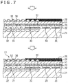
- a light absorbing film 25 is formed in the effective pixel peripheral region 15 as depicted in the upper part of FIG. 7 .
- a pattern edge portion of the light absorbing film 25 is formed so as to have an angular portion as viewed in cross section similarly to the imaging element 11 of FIG. 1 .
- a reflection preventing film 26 is formed over an overall area of the microlenses 52 and the light absorbing film 25 as depicted in the lower part of FIG. 7 .
- an imaging element 11 A of higher quality can be fabricated similarly to the imaging element 11 of FIG. 1 .
- a third embodiment of the imaging element to which the present technology is applied is described with reference to FIG. 8 .
- FIG. 8 depicts an a-a′ cross section of an imaging element 11 B similarly to B of FIG. 1 . Further, in the imaging element 11 B depicted in FIG. 8 , components common to those of the imaging element 11 of FIG. 1 are denoted by the same reference signs, and detailed description of them is omitted.
- the imaging element 11 B is configured such that a semiconductor substrate 21 , a first flattening film 22 , a microlens layer 24 , a light absorbing film 25 , and a reflection preventing film 26 are stacked similarly to the imaging element 11 of FIG. 1 .
- the imaging element 11 B is different from the imaging element 11 of FIG. 1 in the configuration of a color filter layer 23 B.
- the color filter layer 23 B of the imaging element 11 B is configured such that a light absorbing film 37 is formed in the effective pixel peripheral region 15 and the filters 36 of FIG. 1 are not provided.
- the imaging element 11 B is configured such that the pixels 17 can receive light in all wavelength range and output a pixel signal according to the luminance of the received light.
- the imaging element 11 B similarly as in the imaging element 11 of FIG. 1 , in the imaging element 11 B, light incident to the effective pixel peripheral region 15 is absorbed with certainty by the light absorbing film 25 and the light absorbing film 37 thereby to prevent the light from being reflected by the semiconductor substrate 21 to make stray light. Accordingly, the imaging element 11 B can image an image of high picture quality free from flare, ghost, or the like similarly to the imaging element 11 of FIG. 1 .
- the imaging element 11 B configured in this manner not only can be used, for example, in an imaging apparatus that acquires only luminance information of an imaging object but also can be used in an imaging apparatus that includes a plurality of imaging elements 11 B utilizing a light decomposition prism that decomposes a light flux into a plurality of light fluxes.
- FIG. 9 depicts a schematic configuration example of an imaging apparatus that utilizes a light decomposition prism.
- an imaging apparatus 61 includes an objective lens 62 , a light decomposition prism 63 , and imaging elements 11 B- 1 to 11 B- 3 .
- the objective lens 62 condenses incident light incident to the imaging apparatus 61 to form an image of an imaging object on a light reception face of the imaging elements 11 B- 1 to 11 B- 3 .
- the light decomposition prism 63 is configured such that it transmits only light in a specific wavelength range but reflects light outside the wavelength range and spectralizes incident light, for example, into light of red, green, and blue.
- the light decomposition prism 63 transmits light in the wavelength range of green so as to be received by the imaging element 11 B- 2 , reflects light in the wavelength range of red so as to be received by the imaging element 11 B- 1 and reflects light in the wavelength range of blue so as to be received by the imaging element 11 B- 3 .
- the imaging apparatus 61 configured in this manner, in the case where light is reflected in the effective pixel peripheral region 15 of the imaging elements 11 B- 1 to 11 B- 3 , the light is re-reflected in the light decomposition prism 63 and enters as stray light into the effective pixel region 12 of the imaging elements 11 B.
- stray light makes flare, ghost, or the like and becomes a cause that gives rise to deterioration of the picture quality.
- the imaging elements 11 B- 1 to 11 B- 3 are configured such that reflection of light in the effective pixel peripheral region 15 is suppressed, incidence of stray light through the light decomposition prism 63 is avoided, and as a result, an image of high picture quality free from flare, ghost, or the like can be imaged.
- a fourth embodiment of the imaging element to which the present technology is applied is described with reference to FIG. 10 .
- FIG. 10 depicts an a-a′ cross section of an imaging element 11 C similarly so B of FIG. 1 .
- Components of the imaging element 11 C depicted in FIG. 10 common to those of the imaging element 11 of FIG. 1 are denoted by the same reference signs, and detailed description of them is omitted.
- the imaging element 11 C is formed by stacking a semiconductor substrate 21 , a first flattening film 22 , a microlens layer 24 , a light absorbing film 25 , and a reflection preventing film 26 similarly to the imaging element 11 of FIG. 1 .
- the imaging element 11 C is different in configuration of a color filter layer 23 C from the imaging element 11 of FIG. 1 .
- the color filter layer 23 C of the imaging element 11 C is configured such that a light absorbing film 37 is formed in the effective pixel peripheral region 15 and an inter-pixel light blocking film 71 is formed without the provision of the filter 36 of FIG. 1 .
- the inter-pixel light blocking film 71 is disposed between the pixels 17 (at a boundary portion between the pixels 17 ) in the effective pixel region 12 and performs blocking of light for preventing color mixture between the pixels 17 adjacent to each other similarly to the inter-pixel light blocking film 32 .
- an organic material to which a black pigment configured, for example, from carbon black, titanium black, iron oxide (magnetite-based triiron tetroxide), a complex oxide of copper and chromium, a complex oxide of copper, chrome, and zinc, or the like is internally added is used similarly to the light absorbing film 37 .
- the imaging element 11 C can image an image of high picture quality free from flare, ghost, or the like similarly to the imaging element 11 of FIG. 1 .
- a fifth embodiment of the imaging element to which the present technology is applied is described with reference to FIG. 11 .
- FIG. 11 depicts an a-a′ cross section of an imaging element 11 D similarly as in B of FIG. 1 , and in B of FIG. 11 and C of FIG. 11 , layout examples of a grooved portion 72 hereinafter described are depicted.
- Components of the imaging element 11 D depicted in FIG. 11 common to those of the imaging element 11 of FIG. 1 are denoted by the same reference signs, and detailed description of them is omitted.
- the imaging element 11 D is configured by stacking a semiconductor substrate 21 , a first flattening film 22 , a color filter layer 23 , a microlens layer 24 , and a reflection preventing film 26 similarly to the imaging element 11 of FIG. 1 .
- the imaging element 11 B is different from the imaging element 11 of FIG. 1 in configuration of a light absorbing film 25 D.
- the light absorbing film 25 D of the imaging element 11 D is configured such that the grooved portion 72 is formed in the effective pixel peripheral region 15 .
- the grooved portion 72 is formed such that it divides the effective pixel region 12 and the bonding pads 16 formed in the peripheral region 14 from each other.
- the grooved portion 72 can be formed such that it encloses the effective pixel region 12 along an outer periphery of the effective pixel region 12 .
- two grooved portions 72 may be formed along the upper side and the lower side of the effective pixel region 12 .
- the grooved portion 72 on the light absorbing film 25 D in this manner, an angular portion is formed at the opposite ends of the grooved portion 72 as viewed in cross section, and a reflection preventing film 26 is formed along the surface shape of the same. Accordingly, in the case where a crack is generated from an opening provided corresponding to a bonding pad 16 as described hereinabove, the crack can be prevented from progressing to the effective pixel region 12 by an effect of the angle at an edge portion of the grooved portion 72 of the light absorbing film 25 D.
- the imaging element 11 D can improve, compared with the imaging element 11 of FIG. 1 , the effect of preventing a crack generated on the reflection preventing film 26 from progressing to the effective pixel region 12 , and can avoid deterioration of the picture quality by the crack with certainty.
- a sixth embodiment of the imaging element to which the present technology is applied is described with reference to FIG. 12 .
- FIG. 12 depicts a schematic configuration when an imaging element 11 E is viewed in plan similarly to A of FIG. 1
- B of FIG. 12 depicts an a-a′ cross section of the imaging element 11 E similarly so B of FIG. 1 .
- components of the imaging element 11 E depicted in FIG. 12 common to those of the imaging element 11 of FIG. 1 are denoted by the same reference signs, and detailed description of them is omitted.
- the imaging element 11 E is configured by stacking a semiconductor substrate 21 , a first flattening film 22 , and a microlens layer 24 similarly to the imaging element 11 of FIG. 1 .
- FIG. 12 for example, illustration of the OPB region 13 and the peripheral region 14 depicted in FIG. 1 is omitted, and they are collectively depicted as an effective pixel peripheral region 15 , and illustration also of the reflection preventing film 26 is omitted.
- a semiconductor element 101 is mounted on a semiconductor substrate 21 in the effective pixel peripheral region 15 .
- the semiconductor element 101 is mounted by electrically connecting a plurality of land electrodes 102 formed on the semiconductor substrate 21 side and a plurality of land electrodes 103 formed on the semiconductor element 101 side individually through solder bumps 104 . Further, the semiconductor element 101 is adhered by underfill resin 105 filled between the semiconductor element 101 and the microlens layer 24 .
- a light absorbing film 25 E is formed so as to cover the semiconductor element 101 .
- the light absorbing film 25 E is formed such that it includes side faces of the semiconductor element 101 and covers an overall area of the upper face of the semiconductor element 101 .
- the light absorbing film 25 E is formed so as to cover the underfill resin 105 and extend over the microlens layer 24 .
- the imaging element 11 E is configured in this manner and can suppress reflected light in the effective pixel peripheral region 15 by the light absorbing film 25 E. Consequently, for example, where the imaging element 11 E is used in combination with such a light decomposition prism 63 as described above with reference to FIG. 9 , re-reflected light that is generated in the light decomposition prism 63 or light incident as stray light to the effective pixel region 12 of the imaging element 11 E can be reduced. As a result, an image of high picture quality free from flare, ghost, or the like can be imaged by the imaging element 11 E.
- FIG. 13 depicts first to third modifications of the imaging element 11 E.
- an imaging element 11 E-a that is the first modification depicted in A of FIG. 13 is configured such that two semiconductor elements 101 - 1 and 101 - 2 are mounted in the effective pixel peripheral region 15 .
- the imaging element 11 E-a is configured such that the semiconductor element 101 - 1 is disposed along the upper long side of the effective pixel region 12 and the semiconductor element 101 - 2 is disposed along the lower long side of the effective pixel region 12 .
- a light absorbing film 25 E- 1 is formed so as to cover the semiconductor element 101 - 1
- a light absorbing film 25 E- 2 is formed so as to cover the semiconductor element 101 - 2 .
- the light absorbing film 25 E- 1 is formed such that it includes side faces of the semiconductor element 101 - 1 and covers an overall area of the upper face of the semiconductor element 101 - 1
- the light absorbing film 25 E- 2 is formed such that it includes side faces of the semiconductor element 101 - 2 and covers an overall area of the upper face of the semiconductor element 101 - 2 .
- reflected light in the effective pixel peripheral region 15 can be suppressed, and an image of high picture quality free from flare, ghost, or the like can be imaged similarly to the imaging element 11 E.
- an imaging element 11 E-b of the second modification depicted in B of FIG. 13 is configured such that four semiconductor elements 101 - 1 to 101 - 4 are mounted in the effective pixel peripheral region 15 .
- the two semiconductor elements 101 - 1 and 101 - 2 are disposed side by side in a direction along the upper long side of the effective pixel region 12
- the two semiconductor elements 101 - 3 to 101 - 4 are disposed side by side in a direction along the lower long side of the effective pixel region 12 .
- a light absorbing film 25 E- 1 is formed so as to cover the semiconductor elements 101 - 1 and 101 - 2 and a light absorbing film 25 E- 2 is formed so as to cover the semiconductor elements 101 - 3 to 101 - 4 .
- the light absorbing film 25 E- 1 is formed such that it includes side faces of the semiconductor elements 101 - 1 and 101 - 2 and covers an overall area of the upper face of the semiconductor elements 101 - 1 and 101 - 2 .
- the light absorbing film 25 E- 2 is formed so as to include side faces of the semiconductor elements 101 - 3 to 101 - 4 and cover an overall area of the upper face of the semiconductor elements 101 - 3 to 101 - 4 .
- reflected light in the effective pixel peripheral region 15 can be suppressed, and an image of high picture quality free from flare, ghost, or the like can be imaged similarly to the imaging element 11 E.
- an imaging element 11 E-c that is a third modification depicted in C of FIG. 13 is configured such that four semiconductor elements 101 - 1 to 101 - 4 are mounted in the effective pixel peripheral region 15 .
- the semiconductor element 101 - 1 is disposed along the upper long side of the effective pixel region 12
- the semiconductor element 101 - 2 is disposed along the lower long side of the effective pixel region 12 .
- the imaging element 11 E-c is configured such that the semiconductor element 101 - 3 is disposed along the left short side of the effective pixel region 12 and the semiconductor element 101 - 4 is disposed along the right short side of the effective pixel region 12 .
- light absorbing films 25 E- 1 to 25 E- 4 are formed so as to cover the semiconductor elements 101 - 1 to 101 - 4 , respectively.
- the light absorbing films 25 E- 1 to 25 E- 4 are formed so as to include side faces of the semiconductor elements 101 - 1 to 101 - 4 , respectively, and cover an overall area of the upper face of the semiconductor elements 101 - 1 to 101 - 4 , respectively.
- reflected light in the effective pixel peripheral region 15 can be suppressed, and an image of high picture quality free from flare, ghost, or the like can be imaged similarly to the imaging element 11 E.
- a seventh embodiment of the imaging element to which the present technology is applied is described with reference to FIG. 14 .
- a of FIG. 14 depicts a schematic configuration when the imaging element 11 F is viewed in plan similarly to A of FIG. 1
- B of FIG. 14 depicts an a-a′ cross section of the imaging element 11 F of A of FIG. 14 similarly as in B of FIG. 1
- Components of the imaging element 11 F depicted in FIG. 14 common to those of the imaging element 11 of FIG. 1 are denoted by the same reference signs, and detailed description of them is omitted.
- the imaging element 11 F is configured by stacking a semiconductor substrate 21 , a first flattening film 22 , and a microlens layer 24 similarly to the imaging element 11 of FIG. 1 .
- illustration of the OPB region 13 and the peripheral region 14 depicted in FIG. 1 is omitted and they are depicted collectively as effective pixel peripheral region 15 , and also illustration of the reflection preventing film 26 is omitted.
- a semiconductor element 101 is mounted on the semiconductor substrate 21 in the effective pixel peripheral region 15 similarly to the imaging element 11 E of FIG. 12 .
- a light absorbing film 25 F is formed so as to cover the semiconductor element 101 .
- the light absorbing film 25 F is formed so as to include side faces of the semiconductor element 101 at least on the effective pixel region 12 side and cover part of the upper face of the semiconductor element 101 .
- the light absorbing film 25 E is formed such that it covers the underfill resin 105 on the effective pixel region 12 side and extends over the microlens layer 24 on the effective pixel region 12 side.
- the imaging element 11 F is configured in this manner, and can suppress reflected light as is reflected toward the effective pixel region 12 in the effective pixel peripheral region 15 by the light absorbing film 25 F. Consequently, for example, where the imaging element 11 F is used in combination with such a light decomposition prism 63 as described above with reference to FIG. 9 , re-reflected light that is generated in the light decomposition prism 63 or light incident as stray light to the effective pixel region 12 of the imaging element 11 F can be reduced. As a result, an image of high picture quality free from flare, ghost, or the like can be imaged by the imaging element 11 F.
- the imaging element 11 F-a that is a first modification depicted in A of FIG. 15 is configured such that two semiconductor elements 101 - 1 and 101 - 2 are mounted in the effective pixel peripheral region 15 .
- the semiconductor element 101 - 1 is disposed along the upper long side of the effective pixel region 12
- the semiconductor element 101 - 2 is disposed along the lower long side of the effective pixel region 12 .
- a light absorbing film 25 F- 1 is formed so as to cover the semiconductor element 101 - 1
- another light absorbing film 25 F- 2 is formed so as to cover the semiconductor element 101 - 2 .
- the light absorbing film 25 F- 1 is formed so as to include side faces of the semiconductor element 101 at least on the effective pixel region 12 side and cover part of the upper face of the semiconductor element 101 .
- the light absorbing film 25 F- 2 is formed so as to include side faces of the semiconductor element 101 at least on the effective pixel region 12 side and cover part of the upper face of the semiconductor element 101 .
- reflected light in the effective pixel peripheral region 15 can be suppressed, and an image of high picture quality free from flare, ghost, or the like can be imaged similarly to the imaging element 11 F.
- the imaging element 11 F-b that is a second modification depicted in B of FIG. 15 is configured such that four semiconductor elements 101 - 1 to 101 - 4 are mounted in the effective pixel peripheral region 15 .
- the two semiconductor elements 101 - 1 and 101 - 2 are disposed side by side in a direction along the upper long side of the effective pixel region 12
- the two semiconductor elements 101 - 3 to 101 - 4 are disposed side by side in a direction along the lower long side of the effective pixel region 12 .
- a light absorbing film 25 F- 1 is formed so as to cover the semiconductor elements 101 - 1 and 101 - 2
- another light absorbing film 25 F- 2 is formed so as to cover the semiconductor elements 101 - 3 to 101 - 4 .
- the light absorbing film 25 F- 1 is formed so as to include side faces of the semiconductor elements 101 - 1 and 101 - 2 at least on the effective pixel region 12 side and cover part of the upper face of the semiconductor elements 101 - 1 and 101 - 2 .
- the light absorbing film 25 F- 2 is formed so as to include side faces of the semiconductor elements 101 - 3 to 101 - 4 at least on the effective pixel region 12 side and cover part of the upper face of the semiconductor elements 101 - 3 to 101 - 4 .
- reflected light in the effective pixel peripheral region 15 can be suppressed, and an image of high picture quality free from flare, ghost, or the like can be imaged similarly to the imaging element 11 F.
- the imaging element 11 F-c that is a third modification depicted in C of FIG. 15 is configured such that four semiconductor elements 101 - 1 to 101 - 4 are mounted in the effective pixel peripheral region 15 .
- the semiconductor element 101 - 1 is disposed along the upper long side of the effective pixel region 12
- the semiconductor element 101 - 2 is disposed along the lower long side of the effective pixel region 12 .
- the imaging element 11 F-c is configured such that the semiconductor element 101 - 3 is disposed along the left short side of the effective pixel region 12 and the semiconductor element 101 - 4 is disposed along the right short side of the effective pixel region 12 .
- light absorbing films 25 F- 1 to 25 F- 4 are formed so as to cover the semiconductor elements 101 - 1 to 101 - 4 , respectively.
- the light absorbing films 25 F- 1 to 25 F- 4 are formed so as to include side faces of the semiconductor elements 101 - 1 to 101 - 4 at least on the effective pixel region 12 side, respectively, and cover part of the upper face of the semiconductor elements 101 - 1 to 101 - 4 , respectively, as depicted in B of FIG. 14 .
- reflected light in the effective pixel peripheral region 15 can be suppressed, and an image of high picture quality free from flare, ghost, or the like can be imaged similarly to the imaging element 11 F.
- imaging elements 11 as described above can be applied to such various electronic equipment, for example, as imaging systems as a digital still camera or a digital video camera, portable telephone sets including an imaging function, or other equipment including an imaging function.
- FIG. 16 is a block diagram depicting a configuration example of an imaging apparatus incorporated in electronic equipment.
- the imaging apparatus 201 includes an optical system 202 , an imaging element 203 , a signal processing circuit 204 , a monitor 205 , and a memory 206 and can image a still image and a moving image.
- the optical system 202 includes one or a plurality of lenses and introduces image light (incident light) into the imaging element 203 from an imaging object such that an image is formed on a light reception face (sensor section) of the imaging element 203 .
- any of the imaging elements 11 described above is applied.
- electrons are accumulated for a fixed period of time in response to an image formed on the light reception face through the optical system 202 .
- a signal according to the electrons accumulated in the imaging element 203 is supplied to the signal processing circuit 204 .
- the signal processing circuit 204 carries out various signal processes for the pixel signal outputted from the imaging element 203 .
- An image (image data) obtained by the signal processing circuit 204 carrying out the signal processes is supplied to and displayed on the monitor 205 or supplied to and stored (recorded) into the memory 206 .
- an image of higher picture quality can be imaged by applying the imaging element 11 described above.
- FIG. 17 is a view depicting an example of use in which the image sensor described above is used.
- the image sensor described above can be used in various cases in which visible light, infrared light, ultraviolet light, an X ray, or the like is sensed, for example, in the following manner.
- the technology according to the present disclosure can be applied to various products.
- the technology according to the present disclosure may be applied to an endoscopic surgery system.
- FIG. 18 is a view depicting an example of a schematic configuration of an endoscopic surgery system to which the technology according to an embodiment of the present disclosure (present technology) can be applied.
- FIG. 18 a state is illustrated in which a surgeon (medical doctor) 11131 is using an endoscopic surgery system 11000 to perform surgery for a patient 11132 on a patient bed 11133 .
- the endoscopic surgery system 11000 includes an endoscope 11100 , other surgical tools 11110 such as a pneumoperitoneum tube 11111 and an energy device 11112 , a supporting arm apparatus 11120 which supports the endoscope 11100 thereon, and a cart 11200 on which various apparatus for endoscopic surgery are mounted.
- the endoscope 11100 includes a lens barrel 11101 having a region of a predetermined length from a distal end thereof to be inserted into a body cavity of the patient 11132 , and a camera head 11102 connected to a proximal end of the lens barrel 11101 .
- the endoscope 11100 is depicted which includes as a rigid endoscope having the lens barrel 11101 of the hard type.
- the endoscope 11100 may otherwise be included as a flexible endoscope having the lens barrel 11101 of the flexible type.
- the lens barrel 11101 has, at a distal end thereof, an opening in which an objective lens is fitted.
- a light source apparatus 11203 is connected to the endoscope 11100 such that light generated by the light source apparatus 11203 is introduced to a distal end of the lens barrel 11101 by a light guide extending in the inside of the lens barrel 11101 and is irradiated toward an observation target in a body cavity of the patient 11132 through the objective lens.
- the endoscope 11100 may be a forward-viewing endoscope or may be an oblique-viewing endoscope or a side-viewing endoscope.
- An optical system and an image pickup element are provided in the inside of the camera head 11102 such that reflected light (observation light) from the observation target is condensed on the image pickup element by the optical system.
- the observation light is photoelectrically converted by the image pickup element to generate an electric signal corresponding to the observation light, namely, an image signal corresponding to an observation image.
- the image signal is transmitted as RAW data to a CCU 11201 .
- the CCU 11201 includes a central processing unit (CPU), a graphics processing unit (GPU) or the like and integrally controls operation of the endoscope 11100 and a display apparatus 11202 . Further, the CCU 11201 receives an image signal from the camera head 11102 and performs, for the image signal, various image processes for displaying an image based on the image signal such as, for example, a development process (demosaic process).
- a development process demosaic process
- the display apparatus 11202 displays thereon an image based on an image signal, for which the image processes have been performed by the CCU 11201 , under the control of the CCU 11201 .
- the light source apparatus 11203 includes a light source such as, for example, a light emitting diode (LED) and supplies irradiation light upon imaging of a surgical region to the endoscope 11100 .
- a light source such as, for example, a light emitting diode (LED) and supplies irradiation light upon imaging of a surgical region to the endoscope 11100 .
- LED light emitting diode
- An inputting apparatus 11204 is an input interface for the endoscopic surgery system 11000 .
- a user can perform inputting of various kinds of information or instruction inputting to the endoscopic surgery system 11000 through the inputting apparatus 11204 .
- the user would input an instruction or a like to change an image pickup condition (type of irradiation light, magnification, focal distance or the like) by the endoscope 11100 .
- a treatment tool controlling apparatus 11205 controls driving of the energy device 11112 for cautery or incision of a tissue, sealing of a blood vessel or the like.
- a pneumoperitoneum apparatus 11206 feeds gas into a body cavity of the patient 11132 through the pneumoperitoneum tube 11111 to inflate the body cavity in order to secure the field of view of the endoscope 11100 and secure the working space for the surgeon.
- a recorder 11207 is an apparatus capable of recording various kinds of information relating to surgery.
- a printer 11208 is an apparatus capable of printing various kinds of information relating to surgery in various forms such as a text, an image or a graph.
- the light source apparatus 11203 which supplies irradiation light when a surgical region is to be imaged to the endoscope 11100 may include a white light source which includes, for example, an LED, a laser light source or a combination of them.
- a white light source includes a combination of red, green, and blue (RGB) laser light sources, since the output intensity and the output timing can be controlled with a high degree of accuracy for each color (each wavelength), adjustment of the white balance of a picked up image can be performed by the light source apparatus 11203 .
- RGB red, green, and blue
- the light source apparatus 11203 may be controlled such that the intensity of light to be outputted is changed for each predetermined time.
- driving of the image pickup element of the camera head 11102 in synchronism with the timing of the change of the intensity of light to acquire images time-divisionally and synthesizing the images an image of a high dynamic range free from underexposed blocked up shadows and overexposed highlights can be created.
- the light source apparatus 11203 may be configured to supply light of a predetermined wavelength band ready for special light observation.
- special light observation for example, by utilizing the wavelength dependency of absorption of light in a body tissue to irradiate light of a narrow band in comparison with irradiation light upon ordinary observation (namely, white light), narrow band observation (narrow band imaging) of imaging a predetermined tissue such as a blood vessel of a superficial portion of the mucous membrane or the like in a high contrast is performed.
- fluorescent observation for obtaining an image from fluorescent light generated by irradiation of excitation light may be performed.
- fluorescent observation it is possible to perform observation of fluorescent light from a body tissue by irradiating excitation light on the body tissue (autofluorescence observation) or to obtain a fluorescent light image by locally injecting a reagent such as indocyanine green (ICG) into a body tissue and irradiating excitation light corresponding to a fluorescent light wavelength of the reagent upon the body tissue.
- a reagent such as indocyanine green (ICG)
- ICG indocyanine green
- the light source apparatus 11203 can be configured to supply such narrow-band light and/or excitation light suitable for special light observation as described above.
- FIG. 19 is a block diagram depicting an example of a functional configuration of the camera head 11102 and the CCU 11201 depicted in FIG. 18 .
- the camera head 11102 includes a lens unit 11401 , an image pickup unit 11402 , a driving unit 11403 , a communication unit 11404 and a camera head controlling unit 11405 .
- the CCU 11201 includes a communication unit 11411 , an image processing unit 11412 and a control unit 11413 .
- the camera head 11102 and the CCU 11201 are connected for communication to each other by a transmission cable 11400 .
- the lens unit 11401 is an optical system, provided at a connecting location to the lens barrel 11101 . Observation light taken in from a distal end of the lens barrel 11101 is guided to the camera head 11102 and introduced into the lens unit 11401 .
- the lens unit 11401 includes a combination of a plurality of lenses including a zoom lens and a focusing lens.
- the number of image pickup elements which is included by the image pickup unit 11402 may be one (single-plate type) or a plural number (multi-plate type). Where the image pickup unit 11402 is configured as that of the multi-plate type, for example, image signals corresponding to respective R, G and B are generated by the image pickup elements, and the image signals may be synthesized to obtain a color image.
- the image pickup unit 11402 may also be configured so as to have a pair of image pickup elements for acquiring respective image signals for the right eye and the left eye ready for three dimensional (3D) display. If 3D display is performed, then the depth of a living body tissue in a surgical region can be comprehended more accurately by the surgeon 11131 . It is to be noted that, where the image pickup unit 11402 is configured as that of stereoscopic type, a plurality of systems of lens units 11401 are provided corresponding to the individual image pickup elements.
- the image pickup unit 11402 may not necessarily be provided on the camera head 11102 .
- the image pickup unit 11402 may be provided immediately behind the objective lens in the inside of the lens barrel 11101 .
- the driving unit 11403 includes an actuator and moves the zoom lens and the focusing lens of the lens unit 11401 by a predetermined distance along an optical axis under the control of the camera head controlling unit 11405 . Consequently, the magnification and the focal point of a picked up image by the image pickup unit 11402 can be adjusted suitably.
- the communication unit 11404 includes a communication apparatus for transmitting and receiving various kinds of information to and from the CCU 11201 .
- the communication unit 11404 transmits an image signal acquired from the image pickup unit 11402 as RAW data to the CCU 11201 through the transmission cable 11400 .
- the communication unit 11404 receives a control signal for controlling driving of the camera head 11102 from the CCU 11201 and supplies the control signal to the camera head controlling unit 11405 .
- the control signal includes information relating to image pickup conditions such as, for example, information that a frame rate of a picked up image is designated, information that an exposure value upon image picking up is designated and/or information that a magnification and a focal point of a picked up image are designated.
- the image pickup conditions such as the frame rate, exposure value, magnification or focal point may be designated by the user or may be set automatically by the control unit 11413 of the CCU 11201 on the basis of an acquired image signal.
- an auto exposure (AE) function, an auto focus (AF) function and an auto white balance (AWB) function are incorporated in the endoscope 11100 .
- the camera head controlling unit 11405 controls driving of the camera head 11102 on the basis of a control signal from the CCU 11201 received through the communication unit 11404 .
- the communication unit 11411 includes a communication apparatus for transmitting and receiving various kinds of information to and from the camera head 11102 .
- the communication unit 11411 receives an image signal transmitted thereto from the camera head 11102 through the transmission cable 11400 .
- the communication unit 11411 transmits a control signal for controlling driving of the camera head 11102 to the camera head 11102 .
- the image signal and the control signal can be transmitted by electrical communication, optical communication or the like.
- the image processing unit 11412 performs various image processes for an image signal in the form of RAW data transmitted thereto from the camera head 11102 .
- the control unit 11413 performs various kinds of control relating to image picking up of a surgical region or the like by the endoscope 11100 and display of a picked up image obtained by image picking up of the surgical region or the like. For example, the control unit 11413 creates a control signal for controlling driving of the camera head 11102 .
- control unit 11413 controls, on the basis of an image signal for which image processes have been performed by the image processing unit 11412 , the display apparatus 11202 to display a picked up image in which the surgical region or the like is imaged.
- control unit 11413 may recognize various objects in the picked up image using various image recognition technologies.
- the control unit 11413 can recognize a surgical tool such as forceps, a particular living body region, bleeding, mist when the energy device 11112 is used and so forth by detecting the shape, color and so forth of edges of objects included in a picked up image.
- the control unit 11413 may cause, when it controls the display apparatus 11202 to display a picked up image, various kinds of surgery supporting information to be displayed in an overlapping manner with an image of the surgical region using a result of the recognition. Where surgery supporting information is displayed in an overlapping manner and presented to the surgeon 11131 , the burden on the surgeon 11131 can be reduced and the surgeon 11131 can proceed with the surgery with certainty.
- the transmission cable 11400 which connects the camera head 11102 and the CCU 11201 to each other is an electric signal cable ready for communication of an electric signal, an optical fiber ready for optical communication or a composite cable ready for both of electrical and optical communications.
- communication is performed by wired communication using the transmission cable 11400
- the communication between the camera head 11102 and the CCU 11201 may be performed by wireless communication.
- the technology according to the present disclosure can be applied to the endoscope 11100 , (the image pickup unit 11402 of the) camera head 11102 , (the image processing unit 11412 of the) CCU 11201 and so forth from within the configuration described hereinabove.
- the imaging element 11 of FIG. 1 can be applied to the image pickup unit 11402 .
- the technology according to the present disclosure can be applied to various products.
- the technology according to the present disclosure may be applied to an endoscope surgical system.
- FIG. 20 is a block diagram depicting an example of a schematic configuration of an in-vivo information acquisition system of a patient using a capsule type endoscope, to which the technology according to an embodiment of the present disclosure (present technology) can be applied.
- the in-vivo information acquisition system 10001 includes a capsule type endoscope 10100 and an external controlling apparatus 10200 .
- the capsule type endoscope 10100 is swallowed by a patient at the time of inspection.
- the capsule type endoscope 10100 has an image pickup function and a wireless communication function and successively picks up an image of the inside of an organ such as the stomach or an intestine (hereinafter referred to as in-vivo image) at predetermined intervals while it moves inside of the organ by peristaltic motion for a period of time until it is naturally discharged from the patient. Then, the capsule type endoscope 10100 successively transmits information of the in-vivo image to the external controlling apparatus 10200 outside the body by wireless transmission.
- the external controlling apparatus 10200 integrally controls operation of the in-vivo information acquisition system 10001 . Further, the external controlling apparatus 10200 receives information of an in-vivo image transmitted thereto from the capsule type endoscope 10100 and generates image data for displaying the in-vivo image on a display apparatus (not depicted) on the basis of the received information of the in-vivo image.
- an in-vivo image imaged a state of the inside of the body of a patient can be acquired at any time in this manner for a period of time until the capsule type endoscope 10100 is discharged after it is swallowed.
- a configuration and functions of the capsule type endoscope 10100 and the external controlling apparatus 10200 are described in more detail below.
- the capsule type endoscope 10100 includes a housing 10101 of the capsule type, in which a light source unit 10111 , an image pickup unit 10112 , an image processing unit 10113 , a wireless communication unit 10114 , a power feeding unit 10115 , a power supply unit 10116 and a control unit 10117 are accommodated.
- the light source unit 10111 includes a light source such as, for example, a light emitting diode (LED) and irradiates light on an image pickup field-of-view of the image pickup unit 10112 .
- a light source such as, for example, a light emitting diode (LED) and irradiates light on an image pickup field-of-view of the image pickup unit 10112 .
- LED light emitting diode
- the image pickup unit 10112 includes an image pickup element and an optical system including a plurality of lenses provided at a preceding stage to the image pickup element. Reflected light (hereinafter referred to as observation light) of light irradiated on a body tissue which is an observation target is condensed by the optical system and introduced into the image pickup element. In the image pickup unit 10112 , the incident observation light is photoelectrically converted by the image pickup element, by which an image signal corresponding to the observation light is generated. The image signal generated by the image pickup unit 10112 is provided to the image processing unit 10113 .
- the image processing unit 10113 includes a processor such as a central processing unit (CPU) or a graphics processing unit (GPU) and performs various signal processes for an image signal generated by the image pickup unit 10112 .
- the image processing unit 10113 provides the image signal for which the signal processes have been performed thereby as RAW data to the wireless communication unit 10114 .
- the wireless communication unit 10114 performs a predetermined process such as a modulation process for the image signal for which the signal processes have been performed by the image processing unit 10113 and transmits the resulting image signal to the external controlling apparatus 10200 through an antenna 10114 A. Further, the wireless communication unit 10114 receives a control signal relating to driving control of the capsule type endoscope 10100 from the external controlling apparatus 10200 through the antenna 10114 A. The wireless communication unit 10114 provides the control signal received from the external controlling apparatus 10200 to the control unit 10117 .
- a predetermined process such as a modulation process for the image signal for which the signal processes have been performed by the image processing unit 10113 and transmits the resulting image signal to the external controlling apparatus 10200 through an antenna 10114 A. Further, the wireless communication unit 10114 receives a control signal relating to driving control of the capsule type endoscope 10100 from the external controlling apparatus 10200 through the antenna 10114 A. The wireless communication unit 10114 provides the control signal received from the external controlling apparatus 10200 to the control unit 10117 .
- the power feeding unit 10115 includes an antenna coil for power reception, a power regeneration circuit for regenerating electric power from current generated in the antenna coil, a voltage booster circuit and so forth.
- the power feeding unit 10115 generates electric power using the principle of non-contact charging.
- the power supply unit 10116 includes a secondary battery and stores electric power generated by the power feeding unit 10115 .
- FIG. 20 in order to avoid complicated illustration, an arrow mark indicative of a supply destination of electric power from the power supply unit 10116 and so forth are omitted.
- electric power stored in the power supply unit 10116 is supplied to and can be used to drive the light source unit 10111 , the image pickup unit 10112 , the image processing unit 10113 , the wireless communication unit 10114 and the control unit 10117 .
- the control unit 10117 includes a processor such as a CPU and suitably controls driving of the light source unit 10111 , the image pickup unit 10112 , the image processing unit 10113 , the wireless communication unit 10114 and the power feeding unit 10115 in accordance with a control signal transmitted thereto from the external controlling apparatus 10200 .
- a processor such as a CPU and suitably controls driving of the light source unit 10111 , the image pickup unit 10112 , the image processing unit 10113 , the wireless communication unit 10114 and the power feeding unit 10115 in accordance with a control signal transmitted thereto from the external controlling apparatus 10200 .
- the external controlling apparatus 10200 includes a processor such as a CPU or a GPU, a microcomputer, a control board or the like in which a processor and a storage element such as a memory are mixedly incorporated.
- the external controlling apparatus 10200 transmits a control signal to the control unit 10117 of the capsule type endoscope 10100 through an antenna 10200 A to control operation of the capsule type endoscope 10100 .
- an irradiation condition of light upon an observation target of the light source unit 10111 can be changed, for example, in accordance with a control signal from the external controlling apparatus 10200 .
- an image pickup condition (for example, a frame rate, an exposure value or the like of the image pickup unit 10112 ) can be changed in accordance with a control signal from the external controlling apparatus 10200 .
- the substance of processing by the image processing unit 10113 or a condition for transmitting an image signal from the wireless communication unit 10114 (for example, a transmission interval, a transmission image number or the like) may be changed in accordance with a control signal from the external controlling apparatus 10200 .
- the external controlling apparatus 10200 performs various image processes for an image signal transmitted thereto from the capsule type endoscope 10100 to generate image data for displaying a picked up in-vivo image on the display apparatus.
- various signal processes can be performed such as, for example, a development process (demosaic process), an image quality improving process (bandwidth enhancement process, a super-resolution process, a noise reduction (NR) process and/or image stabilization process) and/or an enlargement process (electronic zooming process).
- the external controlling apparatus 10200 controls driving of the display apparatus to cause the display apparatus to display a picked up in-vivo image on the basis of generated image data.
- the external controlling apparatus 10200 may also control a recording apparatus (not depicted) to record generated image data or control a printing apparatus (not depicted) to output generated image data by printing.
- the technology according to the present disclosure can be applied to the image pickup unit 10112 from within the configuration described hereinabove.
- the imaging element 11 of FIG. 1 can be applied to the image pickup unit 10112 .
- the technology according to the present disclosure can be applied to various products.
- the technology according to the present disclosure may be implemented as an apparatus that is incorporated in any type of mobile body such as an automobile, an electric car, a hybrid electric car, a motorcycle, a bicycle, a personal mobility, an airplane, a drone, a ship, or a robot.
- FIG. 21 is a block diagram depicting an example of schematic configuration of a vehicle control system as an example of a mobile body control system to which the technology according to an embodiment of the present disclosure can be applied.
- the vehicle control system 12000 includes a plurality of electronic control units connected to each other via a communication network 12001 .
- the vehicle control system 12000 includes a driving system control unit 12010 , a body system control unit 12020 , an outside-vehicle information detecting unit 12030 , an in-vehicle information detecting unit 12040 , and an integrated control unit 12050 .
- a microcomputer 12051 , a sound/image output section 12052 , and a vehicle-mounted network interface (I/F) 12053 are illustrated as a functional configuration of the integrated control unit 12050 .
- the driving system control unit 12010 controls the operation of devices related to the driving system of the vehicle in accordance with various kinds of programs.
- the driving system control unit 12010 functions as a control device for a driving force generating device for generating the driving force of the vehicle, such as an internal combustion engine, a driving motor, or the like, a driving force transmitting mechanism for transmitting the driving force to wheels, a steering mechanism for adjusting the steering angle of the vehicle, a braking device for generating the braking force of the vehicle, and the like.
- the body system control unit 12020 controls the operation of various kinds of devices provided to a vehicle body in accordance with various kinds of programs.
- the body system control unit 12020 functions as a control device for a keyless entry system, a smart key system, a power window device, or various kinds of lamps such as a headlamp, a backup lamp, a brake lamp, a turn signal, a fog lamp, or the like.
- radio waves transmitted from a mobile device as an alternative to a key or signals of various kinds of switches can be input to the body system control unit 12020 .
- the body system control unit 12020 receives these input radio waves or signals, and controls a door lock device, the power window device, the lamps, or the like of the vehicle.
- the outside-vehicle information detecting unit 12030 detects information about the outside of the vehicle including the vehicle control system 12000 .
- the outside-vehicle information detecting unit 12030 is connected with an imaging section 12031 .
- the outside-vehicle information detecting unit 12030 makes the imaging section 12031 image an image of the outside of the vehicle, and receives the imaged image.
- the outside-vehicle information detecting unit 12030 may perform processing of detecting an object such as a human, a vehicle, an obstacle, a sign, a character on a road surface, or the like, or processing of detecting a distance thereto.
- the imaging section 12031 is an optical sensor that receives light, and which outputs an electric signal corresponding to a received light amount of the light.
- the imaging section 12031 can output the electric signal as an image, or can output the electric signal as information about a measured distance.
- the light received by the imaging section 12031 may be visible light, or may be invisible light such as infrared rays or the like.
- the in-vehicle information detecting unit 12040 detects information about the inside of the vehicle.
- the in-vehicle information detecting unit 12040 is, for example, connected with a driver state detecting section 12041 that detects the state of a driver.
- the driver state detecting section 12041 for example, includes a camera that images the driver.
- the in-vehicle information detecting unit 12040 may calculate a degree of fatigue of the driver or a degree of concentration of the driver, or may determine whether the driver is dozing.
- the microcomputer 12051 can calculate a control target value for the driving force generating device, the steering mechanism, or the braking device on the basis of the information about the inside or outside of the vehicle which information is obtained by the outside-vehicle information detecting unit 12030 or the in-vehicle information detecting unit 12040 , and output a control command to the driving system control unit 12010 .
- the microcomputer 12051 can perform cooperative control intended to implement functions of an advanced driver assistance system (ADAS) which functions include collision avoidance or shock mitigation for the vehicle, following driving based on a following distance, vehicle speed maintaining driving, a warning of collision of the vehicle, a warning of deviation of the vehicle from a lane, or the like.
- ADAS advanced driver assistance system
- the microcomputer 12051 can perform cooperative control intended for automatic driving, which makes the vehicle to travel autonomously without depending on the operation of the driver, or the like, by controlling the driving force generating device, the steering mechanism, the braking device, or the like on the basis of the information about the outside or inside of the vehicle which information is obtained by the outside-vehicle information detecting unit 12030 or the in-vehicle information detecting unit 12040 .
- the microcomputer 12051 can output a control command to the body system control unit 12020 on the basis of the information about the outside of the vehicle which information is obtained by the outside-vehicle information detecting unit 12030 .
- the microcomputer 12051 can perform cooperative control intended to prevent a glare by controlling the headlamp so as to change from a high beam to a low beam, for example, in accordance with the position of a preceding vehicle or an oncoming vehicle detected by the outside-vehicle information detecting unit 12030 .
- the sound/image output section 12052 transmits an output signal of at least one of a sound and an image to an output device capable of visually or auditorily notifying information to an occupant of the vehicle or the outside of the vehicle.
- an audio speaker 12061 a display section 12062 , and an instrument panel 12063 are illustrated as the output device.
- the display section 12062 may, for example, include at least one of an on-board display and a head-up display.
- FIG. 22 is a diagram depicting an example of the installation position of the imaging section 12031 .
- the imaging section 12031 includes imaging sections 12101 , 12102 , 12103 , 12104 , and 12105 .
- the imaging sections 12101 , 12102 , 12103 , 12104 , and 12105 are, for example, disposed at positions on a front nose, sideview mirrors, a rear bumper, and a back door of the vehicle 12100 as well as a position on an upper portion of a windshield within the interior of the vehicle.
- the imaging section 12101 provided to the front nose and the imaging section 12105 provided to the upper portion of the windshield within the interior of the vehicle obtain mainly an image of the front of the vehicle 12100 .
- the imaging sections 12102 and 12103 provided to the sideview mirrors obtain mainly an image of the sides of the vehicle 12100 .
- the imaging section 12104 provided to the rear bumper or the back door obtains mainly an image of the rear of the vehicle 12100 .
- the imaging section 12105 provided to the upper portion of the windshield within the interior of the vehicle is used mainly to detect a preceding vehicle, a pedestrian, an obstacle, a signal, a traffic sign, a lane, or the like.
- FIG. 22 depicts an example of photographing ranges of the imaging sections 12101 to 12104 .
- An imaging range 12111 represents the imaging range of the imaging section 12101 provided to the front nose.
- Imaging ranges 12112 and 12113 respectively represent the imaging ranges of the imaging sections 12102 and 12103 provided to the sideview mirrors.
- An imaging range 12114 represents the imaging range of the imaging section 12104 provided to the rear bumper or the back door.
- a bird's-eye image of the vehicle 12100 as viewed from above is obtained by superimposing image data imaged by the imaging sections 12101 to 12104 , for example.
- At least one of the imaging sections 12101 to 12104 may have a function of obtaining distance information.
- at least one of the imaging sections 12101 to 12104 may be a stereo camera constituted of a plurality of imaging elements, or may be an imaging element having pixels for phase difference detection.
- the microcomputer 12051 can determine a distance to each three-dimensional object within the imaging ranges 12111 to 12114 and a temporal change in the distance (relative speed with respect to the vehicle 12100 ) on the basis of the distance information obtained from the imaging sections 12101 to 12104 , and thereby extract, as a preceding vehicle, a nearest three-dimensional object in particular that is present on a traveling path of the vehicle 12100 and which travels in substantially the same direction as the vehicle 12100 at a predetermined speed (for example, equal to or more than 0 km/hour). Further, the microcomputer 12051 can set a following distance to be maintained in front of a preceding vehicle in advance, and perform automatic brake control (including following stop control), automatic acceleration control (including following start control), or the like. It is thus possible to perform cooperative control intended for automatic driving that makes the vehicle travel autonomously without depending on the operation of the driver or the like.
- automatic brake control including following stop control
- automatic acceleration control including following start control
- the microcomputer 12051 can classify three-dimensional object data on three-dimensional objects into three-dimensional object data of a two-wheeled vehicle, a standard-sized vehicle, a large-sized vehicle, a pedestrian, a utility pole, and other three-dimensional objects on the basis of the distance information obtained from the imaging sections 12101 to 12104 , extract the classified three-dimensional object data, and use the extracted three-dimensional object data for automatic avoidance of an obstacle.
- the microcomputer 12051 identifies obstacles around the vehicle 12100 as obstacles that the driver of the vehicle 12100 can recognize visually and obstacles that are difficult for the driver of the vehicle 12100 to recognize visually. Then, the microcomputer 12051 determines a collision risk indicating a risk of collision with each obstacle.
- the microcomputer 12051 In a situation in which the collision risk is equal to or higher than a set value and there is thus a possibility of collision, the microcomputer 12051 outputs a warning to the driver via the audio speaker 12061 or the display section 12062 , and performs forced deceleration or avoidance steering via the driving system control unit 12010 .
- the microcomputer 12051 can thereby assist in driving to avoid collision.
- At least one of the imaging sections 12101 to 12104 may be an infrared camera that detects infrared rays.
- the microcomputer 12051 can, for example, recognize a pedestrian by determining whether or not there is a pedestrian in imaged images of the imaging sections 12101 to 12104 .
- recognition of a pedestrian is, for example, performed by a procedure of extracting characteristic points in the imaged images of the imaging sections 12101 to 12104 as infrared cameras and a procedure of determining whether or not it is the pedestrian by performing pattern matching processing on a series of characteristic points representing the contour of the object.
- the sound/image output section 12052 controls the display section 12062 so that a square contour line for emphasis is displayed so as to be superimposed on the recognized pedestrian.
- the sound/image output section 12052 may also control the display section 12062 so that an icon or the like representing the pedestrian is displayed at a desired position.
- the technology according to the present disclosure can be applied, for example, to the imaging section 12031 or the like from within the configuration described above.
- the imaging element 11 of FIG. 1 can be applied to the imaging section 12031 .
- An imaging element including:
- a first light absorbing film formed in an effective pixel peripheral region the effective pixel peripheral region being provided so as to enclose an outer side of an effective pixel region in which a plurality of pixels is disposed in a matrix, so as to cover a semiconductor substrate;
- microlens layer provided as an upper layer than the first light absorbing film and having a microlens formed so as to condense light for each of the pixels in the effective pixel region;
- a second light absorbing film provided as an upper layer than the microlens layer and formed in the effective pixel peripheral region.
- the effective pixel peripheral region includes an OPB (Optical Black) region in which a photodiode for outputting a pixel signal for defining a level of a black color that becomes a reference when an image is to be generated is disposed.
- OPB Optical Black
- the first light absorbing film and the second light absorbing film are formed from a material in which at least one of pigments of red, green, blue, yellow, cyan, magenta, gray, and black is internally added.
- an edge portion of the second light absorbing film is formed in such a shape as to have an angular portion as viewed in cross section.
- a plurality of the microlenses formed by an etching method is provided on the microlens layer.
- a plurality of the microlenses formed by a heat reflow method is provided on the microlens layer.
- a filter that transmits light of a color corresponding to each of the pixels is disposed in the effective pixel region in a layer same as that of the first light absorbing film, and a plurality of the pixels provided in the effective pixel region receives light transmitted through the filters.
- the pixels provided in the effective pixel region receives light in all wavelength range.
- an inter-pixel light blocking film for blocking light between a plurality of the pixels is disposed in a layer same as that of the first light absorbing film.
- a grooved portion is formed on the second light absorbing film so as to divide the effective pixel region and a bonding pad provided in the effective pixel peripheral region.
- the second light absorbing film is formed so as to cover a semiconductor element mounted on the semiconductor substrate in the effective pixel peripheral region.
- the second light absorbing film is formed so as to include side faces and cover an overall area of the semiconductor element.
- the second light absorbing film is formed so as to cover side faces of the semiconductor element at least on the effective pixel region side.
- a fabrication method including the steps of:
- the effective pixel peripheral region being provided so as to enclose an outer side of an effective pixel region in which a plurality of pixels is disposed in a matrix, so as to cover a semiconductor substrate;
- microlens layer provided as an upper layer than the first light absorbing film, a microlens for condensing light for each of the pixels in the effective pixel region;
- Electronic equipment including:
- an imaging element including
- Imaging element 11 Imaging element, 12 Effective pixel region, 13 OPB region, 14 Peripheral region, 15 Effective pixel peripheral region, 16 Bonding pad, 17 Pixel, 21 Semiconductor substrate, 22 First flattening film, 23 Color filter layer, 24 Microlens layer, 25 Light absorbing film, 26 Reflection preventing film, 31 Photodiode, 32 Inter-pixel light blocking film, 33 OPB light blocking film, 34 and 35 Wiring line, 36 Filter, 37 Light absorbing film, 38 Microlens
Landscapes
- Physics & Mathematics (AREA)
- Engineering & Computer Science (AREA)
- Power Engineering (AREA)
- General Physics & Mathematics (AREA)
- Electromagnetism (AREA)
- Condensed Matter Physics & Semiconductors (AREA)
- Computer Hardware Design (AREA)
- Microelectronics & Electronic Packaging (AREA)
- Optics & Photonics (AREA)
- Signal Processing (AREA)
- Multimedia (AREA)
- Solid State Image Pick-Up Elements (AREA)
- Transforming Light Signals Into Electric Signals (AREA)
Applications Claiming Priority (7)
| Application Number | Priority Date | Filing Date | Title |
|---|---|---|---|
| JPJP2017-014311 | 2017-01-30 | ||
| JP2017-014311 | 2017-01-30 | ||
| JP2017014311 | 2017-01-30 | ||
| JP2017-183150 | 2017-09-25 | ||
| JP2017183150 | 2017-09-25 | ||
| JPJP2017-183150 | 2017-09-25 | ||
| PCT/JP2018/001087 WO2018139278A1 (fr) | 2017-01-30 | 2018-01-17 | Élément de capture d'image, procédé de fabrication, et dispositif électronique |
Related Parent Applications (1)
| Application Number | Title | Priority Date | Filing Date |
|---|---|---|---|
| PCT/JP2018/001087 A-371-Of-International WO2018139278A1 (fr) | 2017-01-30 | 2018-01-17 | Élément de capture d'image, procédé de fabrication, et dispositif électronique |
Related Child Applications (1)
| Application Number | Title | Priority Date | Filing Date |
|---|---|---|---|
| US17/527,932 Continuation US11670656B2 (en) | 2017-01-30 | 2021-11-16 | Imaging element, fabrication method, and electronic equipment |
Publications (2)
| Publication Number | Publication Date |
|---|---|
| US20210134856A1 US20210134856A1 (en) | 2021-05-06 |
| US11217615B2 true US11217615B2 (en) | 2022-01-04 |
Family
ID=62979494
Family Applications (3)
| Application Number | Title | Priority Date | Filing Date |
|---|---|---|---|
| US16/478,416 Active 2038-08-13 US11217615B2 (en) | 2017-01-30 | 2018-01-17 | Imaging element, fabrication method, and electronic equipment |
| US17/527,932 Active US11670656B2 (en) | 2017-01-30 | 2021-11-16 | Imaging element, fabrication method, and electronic equipment |
| US18/134,208 Pending US20230299102A1 (en) | 2017-01-30 | 2023-04-13 | Imaging element, fabrication method, and electronic equipment |
Family Applications After (2)
| Application Number | Title | Priority Date | Filing Date |
|---|---|---|---|
| US17/527,932 Active US11670656B2 (en) | 2017-01-30 | 2021-11-16 | Imaging element, fabrication method, and electronic equipment |
| US18/134,208 Pending US20230299102A1 (en) | 2017-01-30 | 2023-04-13 | Imaging element, fabrication method, and electronic equipment |
Country Status (2)
| Country | Link |
|---|---|
| US (3) | US11217615B2 (fr) |
| WO (1) | WO2018139278A1 (fr) |
Cited By (1)
| Publication number | Priority date | Publication date | Assignee | Title |
|---|---|---|---|---|
| US11670656B2 (en) | 2017-01-30 | 2023-06-06 | Sony Semiconductor Solutions Corporation | Imaging element, fabrication method, and electronic equipment |
Families Citing this family (10)
| Publication number | Priority date | Publication date | Assignee | Title |
|---|---|---|---|---|
| TW202038456A (zh) | 2018-10-26 | 2020-10-16 | 日商索尼半導體解決方案公司 | 固態攝像元件、固態攝像元件封裝及電子機器 |
| US11688067B2 (en) * | 2019-07-12 | 2023-06-27 | Bruker Nano, Inc. | Methods and systems for detecting defects in devices using X-rays |
| JP2024004503A (ja) * | 2020-11-24 | 2024-01-17 | ソニーセミコンダクタソリューションズ株式会社 | 撮像装置 |
| US11953372B2 (en) | 2021-02-18 | 2024-04-09 | Innolux Corporation | Optical sensing device |
| CN113744641B (zh) * | 2021-08-19 | 2023-04-18 | 惠州华星光电显示有限公司 | 一种显示装置 |
| JP2023077169A (ja) * | 2021-11-24 | 2023-06-05 | ソニーセミコンダクタソリューションズ株式会社 | 発光装置および測距装置 |
| WO2023176122A1 (fr) * | 2022-03-14 | 2023-09-21 | ソニーセミコンダクタソリューションズ株式会社 | Boîtier de semi-conducteur et procédé de fabrication de boîtier de semi-conducteur |
| WO2024048292A1 (fr) * | 2022-08-29 | 2024-03-07 | ソニーセミコンダクタソリューションズ株式会社 | Élément de détection de lumière, dispositif d'imagerie et système de commande de véhicule |
| WO2024105713A1 (fr) * | 2022-11-14 | 2024-05-23 | 三菱電機株式会社 | Détecteur à infrarouge thermique et son procédé de fabrication |
| CN116912432A (zh) * | 2023-09-14 | 2023-10-20 | 安徽农业大学 | 一种高通量植物表型成像方法及成像系统 |
Citations (11)
| Publication number | Priority date | Publication date | Assignee | Title |
|---|---|---|---|---|
| US20080185603A1 (en) * | 2007-02-05 | 2008-08-07 | Matsushita Electric Industrial Co., Ltd. | Optical device and method for manufacturing optical device, and camera module and endoscope module equipped with optical device |
| US20090014824A1 (en) | 2007-07-11 | 2009-01-15 | Matsushita Electric Industrial Co., Ltd. | Solid-state imaging device, method for manufacturing the same, and camera having the device |
| JP2010062417A (ja) | 2008-09-05 | 2010-03-18 | Panasonic Corp | 固体撮像装置およびその製造方法 |
| JP2010085755A (ja) | 2008-09-30 | 2010-04-15 | Fujifilm Corp | カラーフィルタの製造方法及び固体撮像装置 |
| US20120147208A1 (en) * | 2010-12-09 | 2012-06-14 | Sony Corporation | Solid-state imaging device, manufacturing method thereof, and electronic apparatus |
| JP2013012518A (ja) | 2011-06-28 | 2013-01-17 | Toppan Printing Co Ltd | 固体撮像素子 |
| US20130134537A1 (en) | 2011-11-30 | 2013-05-30 | Sony Corporation | Solid-state imaging device and manufacturing method therefor, electronic apparatus, and composition for solid-state imaging device |
| WO2013111419A1 (fr) | 2012-01-26 | 2013-08-01 | シャープ株式会社 | Appareil de capture d'image à semi-conducteurs |
| US20140253756A1 (en) * | 2009-05-11 | 2014-09-11 | Sony Corporation | Two-dimensional solid-state image capture device and polarization-light data processing method therefor |
| US20140367817A1 (en) * | 2013-06-18 | 2014-12-18 | Canon Kabushiki Kaisha | Solid-state imaging apparatus and method for manufacturing the same |
| US20150021729A1 (en) | 2013-07-19 | 2015-01-22 | Sony Corporation | Solid state imaging apparatus and method of producing the same |
Family Cites Families (6)
| Publication number | Priority date | Publication date | Assignee | Title |
|---|---|---|---|---|
| JP2002196104A (ja) * | 2000-12-27 | 2002-07-10 | Seiko Epson Corp | マイクロレンズアレイ及びその製造方法並びに光学装置 |
| JP2003332547A (ja) * | 2002-05-16 | 2003-11-21 | Fuji Film Microdevices Co Ltd | 固体撮像素子及びその製造方法 |
| KR100660319B1 (ko) * | 2004-12-30 | 2006-12-22 | 동부일렉트로닉스 주식회사 | 씨모스 이미지센서 및 그의 제조방법 |
| US8557626B2 (en) * | 2010-06-04 | 2013-10-15 | Omnivision Technologies, Inc. | Image sensor devices and methods for manufacturing the same |
| CN106324784B (zh) * | 2015-06-17 | 2018-11-02 | 玉晶光电(厦门)有限公司 | 具有背胶型遮光组件的镜头 |
| US11217615B2 (en) | 2017-01-30 | 2022-01-04 | Sony Semiconductor Solutions Corporation | Imaging element, fabrication method, and electronic equipment |
-
2018
- 2018-01-17 US US16/478,416 patent/US11217615B2/en active Active
- 2018-01-17 WO PCT/JP2018/001087 patent/WO2018139278A1/fr active Application Filing
-
2021
- 2021-11-16 US US17/527,932 patent/US11670656B2/en active Active
-
2023
- 2023-04-13 US US18/134,208 patent/US20230299102A1/en active Pending
Patent Citations (15)
| Publication number | Priority date | Publication date | Assignee | Title |
|---|---|---|---|---|
| US20080185603A1 (en) * | 2007-02-05 | 2008-08-07 | Matsushita Electric Industrial Co., Ltd. | Optical device and method for manufacturing optical device, and camera module and endoscope module equipped with optical device |
| US20090014824A1 (en) | 2007-07-11 | 2009-01-15 | Matsushita Electric Industrial Co., Ltd. | Solid-state imaging device, method for manufacturing the same, and camera having the device |
| JP2009021379A (ja) | 2007-07-11 | 2009-01-29 | Panasonic Corp | 固体撮像装置およびそれを備えたカメラ、固体撮像装置の製造方法 |
| JP2010062417A (ja) | 2008-09-05 | 2010-03-18 | Panasonic Corp | 固体撮像装置およびその製造方法 |
| JP2010085755A (ja) | 2008-09-30 | 2010-04-15 | Fujifilm Corp | カラーフィルタの製造方法及び固体撮像装置 |
| US20140253756A1 (en) * | 2009-05-11 | 2014-09-11 | Sony Corporation | Two-dimensional solid-state image capture device and polarization-light data processing method therefor |
| JP2012124377A (ja) | 2010-12-09 | 2012-06-28 | Sony Corp | 固体撮像装置とその製造方法、及び電子機器 |
| US20120147208A1 (en) * | 2010-12-09 | 2012-06-14 | Sony Corporation | Solid-state imaging device, manufacturing method thereof, and electronic apparatus |
| JP2013012518A (ja) | 2011-06-28 | 2013-01-17 | Toppan Printing Co Ltd | 固体撮像素子 |
| US20130134537A1 (en) | 2011-11-30 | 2013-05-30 | Sony Corporation | Solid-state imaging device and manufacturing method therefor, electronic apparatus, and composition for solid-state imaging device |
| JP2013115335A (ja) | 2011-11-30 | 2013-06-10 | Sony Corp | 固体撮像素子およびその製造方法、電子機器、並びに固体撮像素子用組成物 |
| WO2013111419A1 (fr) | 2012-01-26 | 2013-08-01 | シャープ株式会社 | Appareil de capture d'image à semi-conducteurs |
| US20140367817A1 (en) * | 2013-06-18 | 2014-12-18 | Canon Kabushiki Kaisha | Solid-state imaging apparatus and method for manufacturing the same |
| US20150021729A1 (en) | 2013-07-19 | 2015-01-22 | Sony Corporation | Solid state imaging apparatus and method of producing the same |
| JP2015023163A (ja) | 2013-07-19 | 2015-02-02 | ソニー株式会社 | 固体撮像装置および固体撮像装置の製造方法。 |
Non-Patent Citations (1)
| Title |
|---|
| International Search Report prepared by the Japan Patent Office dated Mar. 12, 2018, for International Application No. PCT/JP2018/001087. |
Cited By (1)
| Publication number | Priority date | Publication date | Assignee | Title |
|---|---|---|---|---|
| US11670656B2 (en) | 2017-01-30 | 2023-06-06 | Sony Semiconductor Solutions Corporation | Imaging element, fabrication method, and electronic equipment |
Also Published As
| Publication number | Publication date |
|---|---|
| WO2018139278A1 (fr) | 2018-08-02 |
| US11670656B2 (en) | 2023-06-06 |
| US20220077203A1 (en) | 2022-03-10 |
| US20230299102A1 (en) | 2023-09-21 |
| US20210134856A1 (en) | 2021-05-06 |
Similar Documents
| Publication | Publication Date | Title |
|---|---|---|
| US11670656B2 (en) | Imaging element, fabrication method, and electronic equipment | |
| US11424284B2 (en) | Solid-state imaging device and electronic apparatus | |
| WO2019093135A1 (fr) | Élément de capture d'image, procédé de fabrication associé, et appareil électronique | |
| CN110622315B (zh) | 成像装置、固态图像传感器和电子设备 | |
| JP7146376B2 (ja) | 撮像装置、および電子機器 | |
| CN110431668B (zh) | 固态摄像装置和电子设备 | |
| US10868052B2 (en) | Imaging element, manufacturing method, and electronic apparatus | |
| US11647890B2 (en) | Solid-state image pickup element, electronic equipment, and semiconductor apparatus | |
| US11837616B2 (en) | Wafer level lens | |
| EP3936838A1 (fr) | Capteur et instrument de mesure de distance | |
| US20210111213A1 (en) | Imaging device | |
| JP6976751B2 (ja) | 撮像装置および撮像装置の製造方法、並びに、電子機器 | |
| WO2020162196A1 (fr) | Dispositif d'imagerie et système d'imagerie | |
| US11315971B2 (en) | Imaging device, method of producing imaging device, imaging apparatus, and electronic apparatus | |
| CN110998849B (zh) | 成像装置、相机模块和电子设备 | |
| WO2020084973A1 (fr) | Dispositif de traitement d'image | |
| US20240153978A1 (en) | Semiconductor chip, manufacturing method for semiconductor chip, and electronic device | |
| US11735615B2 (en) | Imaging device with protective resin layer and stress relaxation region | |
| US20210272995A1 (en) | Imaging element and electronic apparatus |
Legal Events
| Date | Code | Title | Description |
|---|---|---|---|
| FEPP | Fee payment procedure |
Free format text: ENTITY STATUS SET TO UNDISCOUNTED (ORIGINAL EVENT CODE: BIG.); ENTITY STATUS OF PATENT OWNER: LARGE ENTITY |
|
| AS | Assignment |
Owner name: SONY SEMICONDUCTOR SOLUTIONS CORPORATION, JAPAN Free format text: ASSIGNMENT OF ASSIGNORS INTEREST;ASSIGNOR:OOTSUKA, YOICHI;REEL/FRAME:049844/0772 Effective date: 20190719 |
|
| STPP | Information on status: patent application and granting procedure in general |
Free format text: NON FINAL ACTION MAILED |
|
| STPP | Information on status: patent application and granting procedure in general |
Free format text: NOTICE OF ALLOWANCE MAILED -- APPLICATION RECEIVED IN OFFICE OF PUBLICATIONS |
|
| STPP | Information on status: patent application and granting procedure in general |
Free format text: AWAITING TC RESP, ISSUE FEE PAYMENT VERIFIED |
|
| STPP | Information on status: patent application and granting procedure in general |
Free format text: PUBLICATIONS -- ISSUE FEE PAYMENT VERIFIED |
|
| STCF | Information on status: patent grant |
Free format text: PATENTED CASE |