US11073958B2 - Antenna device - Google Patents
Antenna device Download PDFInfo
- Publication number
- US11073958B2 US11073958B2 US16/073,665 US201716073665A US11073958B2 US 11073958 B2 US11073958 B2 US 11073958B2 US 201716073665 A US201716073665 A US 201716073665A US 11073958 B2 US11073958 B2 US 11073958B2
- Authority
- US
- United States
- Prior art keywords
- antenna
- patterns
- antenna patterns
- layer
- substrates
- Prior art date
- Legal status (The legal status is an assumption and is not a legal conclusion. Google has not performed a legal analysis and makes no representation as to the accuracy of the status listed.)
- Active, expires
Links
- 238000004891 communication Methods 0.000 claims abstract description 32
- 239000000758 substrate Substances 0.000 claims description 37
- 239000002184 metal Substances 0.000 claims description 11
- 229910052751 metal Inorganic materials 0.000 claims description 11
- 238000009792 diffusion process Methods 0.000 claims description 6
- 239000010410 layer Substances 0.000 description 93
- 238000000034 method Methods 0.000 description 13
- 229920002799 BoPET Polymers 0.000 description 12
- 239000000470 constituent Substances 0.000 description 3
- 239000004973 liquid crystal related substance Substances 0.000 description 3
- 238000013459 approach Methods 0.000 description 2
- 230000000903 blocking effect Effects 0.000 description 2
- 230000005684 electric field Effects 0.000 description 2
- 238000005401 electroluminescence Methods 0.000 description 2
- 239000000463 material Substances 0.000 description 2
- 238000012986 modification Methods 0.000 description 2
- 230000004048 modification Effects 0.000 description 2
- 238000000059 patterning Methods 0.000 description 2
- 229920000139 polyethylene terephthalate Polymers 0.000 description 2
- 239000005020 polyethylene terephthalate Substances 0.000 description 2
- 238000012545 processing Methods 0.000 description 2
- 239000002356 single layer Substances 0.000 description 2
- RYGMFSIKBFXOCR-UHFFFAOYSA-N Copper Chemical compound [Cu] RYGMFSIKBFXOCR-UHFFFAOYSA-N 0.000 description 1
- 239000000853 adhesive Substances 0.000 description 1
- 230000001070 adhesive effect Effects 0.000 description 1
- 229910052802 copper Inorganic materials 0.000 description 1
- 239000010949 copper Substances 0.000 description 1
- 239000006059 cover glass Substances 0.000 description 1
- 230000000694 effects Effects 0.000 description 1
- 238000003475 lamination Methods 0.000 description 1
- 230000035699 permeability Effects 0.000 description 1
- -1 polyethylene terephthalate Polymers 0.000 description 1
- 239000011347 resin Substances 0.000 description 1
- 229920005989 resin Polymers 0.000 description 1
Images


Classifications
-
- G—PHYSICS
- G06—COMPUTING; CALCULATING OR COUNTING
- G06F—ELECTRIC DIGITAL DATA PROCESSING
- G06F3/00—Input arrangements for transferring data to be processed into a form capable of being handled by the computer; Output arrangements for transferring data from processing unit to output unit, e.g. interface arrangements
- G06F3/01—Input arrangements or combined input and output arrangements for interaction between user and computer
- G06F3/03—Arrangements for converting the position or the displacement of a member into a coded form
- G06F3/041—Digitisers, e.g. for touch screens or touch pads, characterised by the transducing means
- G06F3/046—Digitisers, e.g. for touch screens or touch pads, characterised by the transducing means by electromagnetic means
-
- G—PHYSICS
- G06—COMPUTING; CALCULATING OR COUNTING
- G06K—GRAPHICAL DATA READING; PRESENTATION OF DATA; RECORD CARRIERS; HANDLING RECORD CARRIERS
- G06K7/00—Methods or arrangements for sensing record carriers, e.g. for reading patterns
- G06K7/10—Methods or arrangements for sensing record carriers, e.g. for reading patterns by electromagnetic radiation, e.g. optical sensing; by corpuscular radiation
- G06K7/10009—Methods or arrangements for sensing record carriers, e.g. for reading patterns by electromagnetic radiation, e.g. optical sensing; by corpuscular radiation sensing by radiation using wavelengths larger than 0.1 mm, e.g. radio-waves or microwaves
- G06K7/10297—Methods or arrangements for sensing record carriers, e.g. for reading patterns by electromagnetic radiation, e.g. optical sensing; by corpuscular radiation sensing by radiation using wavelengths larger than 0.1 mm, e.g. radio-waves or microwaves arrangements for handling protocols designed for non-contact record carriers such as RFIDs NFCs, e.g. ISO/IEC 14443 and 18092
-
- H—ELECTRICITY
- H01—ELECTRIC ELEMENTS
- H01Q—ANTENNAS, i.e. RADIO AERIALS
- H01Q1/00—Details of, or arrangements associated with, antennas
- H01Q1/36—Structural form of radiating elements, e.g. cone, spiral, umbrella; Particular materials used therewith
- H01Q1/38—Structural form of radiating elements, e.g. cone, spiral, umbrella; Particular materials used therewith formed by a conductive layer on an insulating support
-
- H—ELECTRICITY
- H01—ELECTRIC ELEMENTS
- H01Q—ANTENNAS, i.e. RADIO AERIALS
- H01Q7/00—Loop antennas with a substantially uniform current distribution around the loop and having a directional radiation pattern in a plane perpendicular to the plane of the loop
-
- H—ELECTRICITY
- H04—ELECTRIC COMMUNICATION TECHNIQUE
- H04B—TRANSMISSION
- H04B5/00—Near-field transmission systems, e.g. inductive loop type
- H04B5/0025—Near field system adaptations
-
- H04B5/43—
-
- H04B5/70—
-
- H—ELECTRICITY
- H01—ELECTRIC ELEMENTS
- H01Q—ANTENNAS, i.e. RADIO AERIALS
- H01Q1/00—Details of, or arrangements associated with, antennas
- H01Q1/12—Supports; Mounting means
- H01Q1/22—Supports; Mounting means by structural association with other equipment or articles
- H01Q1/2208—Supports; Mounting means by structural association with other equipment or articles associated with components used in interrogation type services, i.e. in systems for information exchange between an interrogator/reader and a tag/transponder, e.g. in Radio Frequency Identification [RFID] systems
- H01Q1/2216—Supports; Mounting means by structural association with other equipment or articles associated with components used in interrogation type services, i.e. in systems for information exchange between an interrogator/reader and a tag/transponder, e.g. in Radio Frequency Identification [RFID] systems used in interrogator/reader equipment
Definitions
- the present invention relates to an antenna device that includes antenna patterns for near field wireless communication and reads information via near field wireless communication.
- the following technique is often used: between an IC card (contactless IC card) that does not include a power source and incorporates an antenna element for wireless communication, and a communication device that includes a power source, near field communication is performed between the IC card and the communication device without the two being brought into contact with each other.
- near field communication is performed between the IC card and the communication device without the two being brought into contact with each other.
- the contactless IC card is brought close to the communication device, to such an extent that the distance between the antenna element of the communication device and the contactless IC card is equal to or less than a predetermined distance.
- the communication device includes a power source, and power is supplied to the antenna element for near field wireless communication incorporated in the communication device, whereby a magnetic field is generated by the antenna element. Then, by the magnetic field generated by the communication device when the contactless IC card is brought close to the communication device, induced current is caused to flow through the antenna element of the contactless IC card. Thus, electric power can be supplied from the communication device to the contactless IC card. Then, the contactless IC card causes a circuit (for example, an IC chip) in the contactless IC card to operate, with use of the electromotive force generated by the induced current. In this way, by bringing a contactless IC card close to a communication device, wireless communication (near field communication) can be performed between the contactless IC card and the communication device.
- a circuit for example, an IC chip
- Patent Document 1 Such an antenna device in which an antenna element is incorporated in a display terminal is disclosed in Patent Document 1.
- the display terminal disclosed in Patent Document 1 when a touch operation is performed by an IC card with respect to the display area, data are transmitted/received between the display terminal and an IC card reader/writer via an antenna coil at the touch operation position, and at the same time, control corresponding to display contents displayed on the display terminal is performed in correspondence to the touch operation position.
- FIG. 11 illustrates an exemplary case where one antenna line passes through the midpoint of the IC card, but in a case of a coil-form antenna, the identical phenomenon occurs when the midpoint of the IC card is positioned at the center of the bunch of a plurality of antenna lines that form the coil. This leads to the problem that there is unavoidably an insensitive area on the touch surface on which a touch operation by an IC card or the like is performed.
- an object of the present invention to provide an antenna device that includes a plurality of antenna patterns and reads information via near field wireless communication, wherein a touch surface of the antenna device has no insensitive area.
- an antenna device is an antenna device that reads information via near field wireless communication, and the antenna device includes an antenna layer that includes a plurality of antenna patterns arrayed in parallel with one another, wherein at least a part of the antenna patterns are arranged so as to overlap with one another when the antenna layer is viewed in a plan view.
- the antenna patterns are arranged so as to overlap with one another when the antenna layer is viewed in a plan view. Accordingly, even if an object to be read is located at such a position at which the reading of the object cannot be performed by one antenna pattern, the possibility that the reading of the object can be performed by an antenna pattern that is adjacent to and overlaps with the foregoing antenna pattern is increased.
- an antenna device that includes a plurality of antenna patterns and reads information via near field wireless communication, wherein a touch surface of the antenna device has no insensitive area.
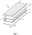
- FIG. 1 is an exploded perspective view illustrating a schematic configuration of an antenna device in Embodiment 1.
- FIG. 2 is a cross-sectional view illustrating a state of the antenna device according to Embodiment 1, taken along a cross section parallel to the Y-Z plane.
- FIG. 3 is a cross-sectional view illustrating a state of a modification example of the antenna device according to Embodiment 1, taken along a cross section parallel to the Y-Z plane.
- FIG. 4 is a schematic plan view schematically illustrating an arrangement of antenna patterns in an antenna layer.
- FIG. 5 is a schematic plan view illustrating an exemplary configuration of antenna patterns.
- FIG. 6 is exploded perspective view illustrating a schematic configuration of an antenna device in Embodiment 2.
- FIG. 7 is a cross-sectional view illustrating a state of the antenna device according to Embodiment 2, taken along a cross section parallel to the Y-Z plane.
- FIG. 8 is a cross-sectional view illustrating a state of a modification example of the antenna device according to Embodiment 2, taken along a cross section parallel to the Y-Z plane.
- FIG. 9 is a schematic plan view schematically illustrating an arrangement of antenna patterns in an antenna layer in Embodiment 2.
- FIG. 10 is a schematic plan view illustrating an exemplary configuration of antenna patterns.
- FIG. 11 ( a ) and ( b ) of FIG. 11 schematically illustrate states of a conventional antenna device in which an IC card cannot be detected.
- An antenna device is an antenna device that reads information via near field wireless communication, and the antenna device includes an antenna layer that includes a plurality of antenna patterns arrayed in parallel with one another, wherein at least a part of the antenna patterns are arranged so as to overlap with one another when the antenna layer is viewed in a plan view (the first configuration).
- the antenna patterns are arranged so as to overlap with one another when the antenna layer is viewed in a plan view.
- the first configuration is further characterized in that at least a part of the antenna patterns are arranged so as to be shifted by half pitch (the second configuration).
- the antenna patterns can be arranged regularly and efficiently.
- the first or second configuration is further characterized in further including FPC substrates that are connected with the antenna patterns at both ends in a second direction that intersects with the first direction, wherein, in a portion where antenna lines of adjacent ones of the antenna patterns intersect with each other when viewed in a plan view, either one of the antenna lines is arranged through a contact hole formed in the FPC substrate (the third configuration).
- the antenna lines of adjacent ones of the antenna patterns can be arranged so as to intersect with each other in the FPC substrate area, without contact with each other.
- any one of the first to third configurations is further characterized in that the antenna pattern is formed in a loop form or in a spiral form wound twice or more (the fourth configuration).
- any one of the first to fourth configurations is further characterized in that two of the antenna layers are provided, wherein the two antenna layers are arranged in such a manner that a direction in which the antenna patterns included in one of the two antenna layers are arrayed, and a direction in which the antenna patterns included in the other antenna layer are arrayed, intersect at right angles (the fifth configuration).
- Any one of the first to fifth configurations may further include a display panel (the sixth configuration).
- a display device having a near field wireless communication function can be provided.
- the sixth configuration is preferably further characterized in further including a light diffusion film provided between the display panel and the antenna layer (the seventh configuration).
- the sixth or seventh configuration may be characterized in further including a touch panel (the eighth configuration).
- a touch-panel-equipped display device having a near field wireless communication function can be provided.
- any one of the first to eighth configuration can be characterized in that the antenna layer is made of a transparent metal or a metal that is patterned in a mesh form (the ninth configuration).
- the antenna device according to this ninth configuration it is possible to prevent the antenna layer from blocking light, particularly in a case where the antenna layer is laminated with a display panel, a touch panel, or the like.
- Embodiment 1 is an antenna device that is configured as a display device including a touch panel and an antenna element.
- FIG. 1 is an exploded perspective view illustrating a schematic configuration of an antenna device 1 in Embodiment 1.
- the antenna device 1 includes a touch panel 10 , an antenna layer 20 and a display panel 30 .
- the antenna device 1 detects the touch position with the touch panel 10 , and performs a processing operation corresponding to an object displayed at the touch position.
- the antenna layer 20 reads information of the IC card in a non-contact state, and performs a corresponding processing operation.
- the antenna device according to the present embodiment can be subjected to both types of input operations, i.e., input by a touch operation with a finger, a pen, or the like, and input by reading of an IC card.
- the display panel 30 is, for example, a liquid crystal panel.
- An embodiment in which the display panel 30 is a liquid crystal panel is described as the present embodiment, but the display panel 30 is not limited to a liquid crystal panel.
- An arbitrary display panel can be used as the display panel 30 as long as it is a panel that has a function of displaying an image, such as an organic electroluminescence (EL) panel.
- EL organic electroluminescence
- FIG. 1 the illustration of known members of the display panel 30 such as a backlight is omitted, and detailed descriptions of the same are omitted hereinafter as well.
- the touch panel 10 includes a first electrode layer 11 and a second electrode layer 12 .
- the first electrode layer 11 includes X-direction electrode patterns Ex formed on a substrate made of an insulative material (for example, polyethylene terephthalate (PET)).
- PET polyethylene terephthalate
- the number of X-direction electrode patterns Ex is arbitrary.
- the X-direction electrode patterns Ex are, for example, transparent conductive patterns (transparent electrodes) formed with ITO or the like. Further, the X-direction electrode patterns Ex may be formed with mesh patterns of thin metal wires (for example, copper). By forming the X-direction electrode patterns Ex in this way, it can be made sure to prevent the X-direction electrode patterns Ex from blocking light (to ensure a certain level of light permeability).
- the second electrode layer 12 includes a plurality of Y-direction electrode patterns Ey extending along the Y direction, which intersect with the X-direction electrode patterns Ex at right angles.
- the Y-direction electrode patterns Ey are made of a material identical to that for the X-direction electrode patterns Ex.
- the number of the Y-direction electrode patterns Ey is also arbitrary.
- Each X-direction electrode pattern Ex has a shape elongated in the X direction.
- Each Y-direction electrode pattern Ey has a shape elongated in the Y direction.
- Each of the X-direction electrode patterns Ex and the Y-direction electrode patterns Ey is connected to a touch panel controller (not illustrated) via a lead line.
- the touch panel controller outputs a driving signal for sequentially driving the X-direction electrode patterns Ex, thereby driving the X-direction electrode patterns Ex sequentially. This causes electric fields to be generated between the X-direction electrode patterns Ex and the Y-direction electrode patterns Ey.
- the touch panel controller receives sense signals from the Y-direction electrode patterns Ey, and checks the signal values of the sense signals, thereby detecting a touch point (a portion where the electric field has changed) on the touch panel surface.
- the antenna layer 20 a plurality of antenna patterns are formed.
- the antenna patterns in the antenna layer 20 are described in details later.
- FIG. 2 is a cross-sectional view illustrating the antenna device 1 , taken along a cross section parallel to the Y-Z plane.
- the first electrode layer 11 has the X-direction electrode patterns Ex on one surface of a PET film 11 a .
- the second electrode layer 12 includes Y-direction electrode patterns Ey on one surface of a PET film 12 a . Incidentally, though FIG.
- the configuration may be such that the X-direction electrode pattern Ex of the first electrode layer 11 and the Y-direction electrode patterns Ey of the second electrode layer 12 are formed on each surface of one PET film, respectively.
- the antenna patterns 21 are formed on one surface of the PET film 22 .
- flexible printed circuit (FPC) substrates 23 are connected to both ends in the Y direction of the antenna layer 20 .
- an optically clear resin (OCR) layer 46 Between the display panel 30 and the antenna layer 20 , there are provided an optically clear resin (OCR) layer 46 , a protection PET film 45 , and an optically clear adhesive (OCA) layer 44 .
- OCR layer 46 and the OCA layer 44 have a function of filling the clearances between the display panel 30 , the protection PET film 45 , and the antenna layer 20 , and at the same time, a function of adjusting the refractive index, and the like.
- the configuration may be such that a light diffusion film 47 is included in place of the protection PET film 45 illustrated in FIG. 2 .
- a light diffusion film 47 is included in place of the protection PET film 45 illustrated in FIG. 2 .
- a lead line (not shown) is drawn from one end in the X direction of each X-direction electrode pattern Ex on the touch panel 10 , and a lead line 12 b is drawn from each Y-direction electrode pattern Ey.
- the lead lines are connected to the above-described touch panel controller (not shown).
- an OCA layer 42 and a cover glass 41 are laminated.
- FIGS. 1 to 3 The configuration illustrated in FIGS. 1 to 3 is, however, merely one example, and other arbitrary constituent members can be add as required. Further, in the configuration illustrated in FIGS. 1 to 3 , the first electrode layer 11 in which the X-direction electrode patterns Ex are formed is arranged on the front surface side, and the second electrode layer 12 is arranged between the first electrode layer 11 and the antenna layer 20 , but the order of lamination of the first electrode layer 11 and the second electrode layer 12 may be reverse to this.
- the following description describes the arrangement of the antenna patterns 21 in the antenna layer 20 while referring to FIG. 4 .
- a plurality of antenna patterns are formed so as to overlap with one another. More specifically, as illustrated in FIG. 4 , the antenna patterns 21 a , 21 b , 21 c , 21 d , 21 e , . . . , 21 k , 21 l are formed so as to overlap with one another while being successively shifted by half pitch. More specifically, the arrangement is such that the center line of the clearance between the antenna pattern 21 a and the antenna pattern 21 c falls on the center line of the antenna pattern 21 b .
- antenna patterns 21 an exemplary configuration that includes twelve antenna patterns is illustrated, but the configuration is not limited to this; the number of antenna patterns is arbitrary. In the description below, in a case where it is not necessary to distinguish individual antenna patterns among the antenna patterns 21 , the antenna patterns are generally referred to as “antenna patterns 21 ”.
- the rectangular shapes illustrated in FIG. 4 indicating the antenna patterns 21 a , 21 b . . . schematically illustrate respective areas where the individual antenna coils are arranged, and do not illustrate actual shapes of the antenna lines.
- Each actual antenna coil is arranged as an antenna coil in a loop form or in a spiral form wound twice or more in each of these areas.
- the antenna coil can be formed by patterning a transparent metal.
- a metal mesh laid over an entirety of the antenna layer 20 may be notched so that appropriate patterns are obtained, whereby antenna coils can be formed.
- the antenna patterns can be made less visible.
- FIG. 5 is a schematic plan view illustrating exemplary antenna patterns 21 .
- FIG. 5 illustrates the antenna patterns 21 a to 21 g , and the illustration of the other antenna patterns is omitted.
- the antenna patterns 21 a to 21 g are formed so as to overlap while being shifted by half pitch.
- the arrangement is such that the center line of the clearance between the antenna pattern 21 a and the antenna pattern 21 c falls on the center line of the antenna pattern 21 b.
- Each antenna pattern 21 is formed as an antenna coil in a loop form or in a spiral form wound twice or more, as described above.
- the antenna line is formed in a linear form extending in the Y direction. More specifically, in the pixel region DP, each antenna line does not intersect with adjacent one of the antenna lines, but is arranged in parallel in the Y direction.
- the antenna lines reaching the surface of the FPC substrates 23 extend along the X direction. Then, in each portion on the FPC substrate 23 where antenna lines of adjacent ones of the antenna patterns intersect with each other when viewed in a plan view, the antenna line of either one of the antenna patterns goes through a contact hole formed in the FPC substrate 23 to be arranged in another layer of the FPC substrate 23 . This makes it possible to cause antenna lines of adjacent ones of the antenna patterns to intersect with each other in the FPC substrate areas.
- a portion extending in the X direction of the antenna pattern 21 is preferably arranged, not in the pixel region DP, but on the FPC substrate 23 . With this configuration, all of the antenna lines are arranged in parallel in the Y direction in the pixel region DP, which makes the antenna lines less visible.
- the antenna patterns 21 are connected with an antenna controller (not shown) via the FPC substrates 23 .
- the antenna controller sequentially applies a driving signal to the antenna patterns 21 a , 21 b , 21 c , 21 d , 21 e , . . . , 21 k , 21 l .
- the driving is performed with a sinusoidal wave of 13.56 megahertz.
- the adjacent ones of the antenna patterns overlap with each other. Even if, therefore, an IC card touches in such a manner that the midpoint of the IC card is positioned on the antenna line of one antenna pattern of the antenna patterns 21 a , 21 b , 21 c , 21 d , 21 e , . . . , 21 k , 21 l , the IC card can be detected by an antenna pattern adjacent thereto.
- the method for driving the antenna patterns 21 may be, not the above-described method of sequentially driving all of the antenna patterns as described above, but a method of simultaneously driving two of the antenna patterns that are located at distanced positions.
- the method is such that the antenna patterns 21 a and 21 d are simultaneously driven, and subsequently, the antenna patterns 21 b and 21 e , the antenna patterns 21 c and 21 f , the antenna patterns 21 d and 21 g , the antenna patterns 21 e and 21 h , the antenna patterns 21 f and 21 i , the antenna patterns 21 g and 21 j , the antenna patterns 21 h and 21 k , and the antenna patterns 21 i and 21 l are sequentially driven at a given cycle. Adjacent ones of the antenna patterns are sequentially driven by such a driving method as well, which allows an IC card that cannot be detected one antenna pattern to be detected by another adjacent thereto.
- the antenna patterns 21 are arranged so as to overlap with one another when the antenna layer 20 is viewed in a plan view, whereby an IC card located at such a position that it cannot be detected by one antenna pattern can be detected by another antenna pattern adjacent thereto. This makes it possible to realize a device in which there is no insensitive area throughout the entire display area, thereby to improve the usability. Further, since the antenna layer 20 is a line layer composed of a single layer, it can be manufactured at a lower cost.
- the arrangement of the antenna patterns 21 is not limited to this arrangement. Any configuration is acceptable as long as, among a plurality of antenna patterns, at least a part of the antenna patterns are arranged so that each overlaps with an adjacent one, and the interval is not limited to half pitch.
- Embodiment 2 is an antenna device that has a configuration of a display device including a touch panel and an antenna element.
- FIG. 6 is an exploded perspective view illustrating a schematic configuration of an antenna device 2 in Embodiment 2. As illustrated in FIG. 2 , the antenna device 2 is different from the antenna device 1 according to Embodiment 1 in the point that the antenna device 2 further includes an antenna layer 50 in addition to the antenna layer 20 in Embodiment 1 mentioned above.
- the antenna layer 20 includes a plurality of antenna patterns 21 that are arrayed along the X direction, so that the position in the X direction of the IC card can be detected.
- the antenna layer 50 includes a plurality of antenna patterns 51 that are arrayed along the Y direction, so that the position in the Y direction of the IC card can be detected.
- the antenna layer 50 at both ends thereof in the X direction, is connected to FPC substrates 52 . In this way, when an IC card touches the pixel region DP, the antenna device 2 , which includes the two antenna layers according to the present embodiment, is capable of detecting the X, Y coordinates of the touch position.
- FIG. 7 is a cross-sectional view illustrating a state of the antenna device 2 , taken along a cross section parallel to the Y-Z plane.
- the antenna device 2 includes an antenna layer 50 between the antenna layer 20 and the touch panel 10 .
- the antenna layer 50 includes antenna patterns 51 on one surface of a PET film 52 .
- the example illustrated in FIG. 7 is an exemplary configuration in which the antenna patterns 21 in the antenna layer 20 and the antenna patterns 51 in the antenna layer 50 are formed on different PET films, respectively, but the configuration may be such that the antenna patterns 21 in the antenna layer 20 and the antenna patterns 51 in the antenna layer 50 are formed on both surfaces of one PET film, respectively.
- FIG. 7 illustrates an exemplary configuration in which the antenna layer 50 is interposed between the antenna layer 20 and the touch panel 10 , the positions of the antenna layer 20 and the antenna layer 50 may be reversed.
- the configuration may be such that a light diffusion film 47 is included in place of the protection PET film 45 illustrated in FIG. 7 .
- a light diffusion film 47 is included in place of the protection PET film 45 illustrated in FIG. 7 .
- the antenna patterns 51 in the antenna layer 50 are arranged so as to overlap with the adjacent antenna patterns while being shifted by half pitch, as is the case with the antenna patterns 21 in the antenna layer 20 .
- an exemplary configuration in which twelve antenna patterns 51 a , 51 b , . . . 51 l are included is disclosed, but the configuration is not limited to this.
- the number of the antenna patterns in the antenna layer 50 is arbitrary. In the description below, in a case where it is not necessary to distinguish individual antenna patterns among the antenna patterns 51 , the antenna patterns are generally referred to as “antenna patterns 51 ”.
- the rectangular shapes illustrated in FIG. 9 indicating the antenna patterns 51 a , 51 b . . . schematically illustrate respective areas where the individual antenna coils are arranged, and do not illustrate actual shapes of the antenna lines.
- Each actual antenna coil is arranged as an antenna coil in a loop form or in a spiral form wound twice or more in each of these areas.
- the antenna coil can be formed by patterning a transparent metal.
- a metal mesh laid over an entirety of the antenna layer 50 may be notched so that appropriate patterns are obtained, whereby antenna coils can be formed.
- the antenna patterns can be made less visible.
- FIG. 10 is a schematic plan view illustrating exemplary antenna patterns 51 .
- FIG. 10 illustrates the antenna patterns 51 a to 51 e , and the illustration of the other antenna patterns is omitted.
- the antenna patterns 51 a to 51 e are formed so as to overlap while being shifted by half pitch.
- the arrangement is such that the center line of the clearance between the antenna pattern 51 a and the antenna pattern 51 c falls on the center line of the antenna pattern 51 b.
- Each antenna pattern 51 is formed as an antenna coil in a loop form or in a spiral form wound twice or more, as described above.
- the antenna line is formed in a linear form extending in the X direction. More specifically, in the pixel region DP, each antenna line of the antenna patterns 51 does not intersect with adjacent one of the antenna lines, but is arranged in parallel in the X direction.
- the antenna lines reaching the surface of the FPC substrates 53 extend along the Y direction. Then, in each portion on the FPC substrate 53 where antenna lines of adjacent ones of the antenna patterns intersect with each other when viewed in a plan view, the antenna line of either one of the antenna patterns goes through a contact hole formed in the FPC substrate 53 to be arranged in another layer of the FPC substrate 53 . This makes it possible to cause antenna lines of adjacent ones of the antenna patterns to intersect with each other in the FPC substrate areas.
- a portion extending in the Y direction of the antenna pattern 51 is preferably arranged, not in the pixel region DP, but on the FPC substrate 53 . With this configuration, all of the antenna lines are arranged in parallel in the X direction in the pixel region DP, which makes the antenna lines less visible.
- the method for driving the antenna patterns 51 in the antenna layer 50 is identical to the method for driving the antenna patterns 21 .
- the touch panel controller sequentially applies a driving signal to the antenna patterns 51 a , 51 b . 51 c . 51 d , 51 e , . . . , 51 k , 51 l .
- the method for driving the antenna patterns 51 may be, not the above-described method of sequentially driving all of the antenna patterns 51 in this way, but a method of simultaneously driving two of the antenna patterns that are located at distanced positions.
- the method is such that the antenna patterns 51 a and 51 d are simultaneously driven, and subsequently, the antenna patterns 51 b and 51 e , the antenna patterns 51 c and 51 f , the antenna patterns 51 d and 51 g , the antenna patterns 51 e and 51 h , the antenna patterns 51 f and 51 i , the antenna patterns 51 g and 51 j , the antenna patterns 51 h and 51 k , and the antenna patterns 51 i and 51 l are sequentially driven at a given cycle. Adjacent ones of the antenna patterns are sequentially driven by these driving methods, which allows an IC card that cannot be detected one antenna pattern to be detected by another adjacent one of the antenna patterns.
- the X coordinate of the IC card can be detected by the antenna layer 20
- the Y coordinate of the IC card can be detected by the antenna layer 50 , respectively, with high accuracy.
- the antenna layer 20 is a line layer composed of a single layer, and so is the antenna layer 50 , these layers can be manufactured at a lower cost.
- the arrangement of the antenna patterns 21 and 51 is not limited to this arrangement. Any configuration is acceptable as long as, among a plurality of antenna patterns, at least a part of the antenna patterns are arranged so that each overlaps with an adjacent one, and the interval is not limited to half pitch.
- Embodiments 1 and 2 are described with reference to an exemplary case where the antenna device of the present invention is formed as a touch-panel-equipped display device.
- a touch panel and a display device are not essential, and the present invention can be implemented as an IC card reader for reading information from an IC card that is caused to approach to the IC card reader.
- the configuration of the touch panel is not limited to that disclosed herein, and a touch panel of an arbitrary configuration (for example, an optical-type touch panel, a resistance-film-type touch panel) can be adopted.
- an IC card and an NFC card are mentioned in the foregoing description as examples of objects from which information is to be read out by near field wireless communication, an object to be read is not limited to a card, and a variety of types can be adopted.
Applications Claiming Priority (4)
| Application Number | Priority Date | Filing Date | Title |
|---|---|---|---|
| JPJP2016-015629 | 2016-01-29 | ||
| JP2016-015629 | 2016-01-29 | ||
| JP2016015629 | 2016-01-29 | ||
| PCT/JP2017/002857 WO2017131129A1 (ja) | 2016-01-29 | 2017-01-27 | アンテナデバイス |
Publications (2)
| Publication Number | Publication Date |
|---|---|
| US20190042811A1 US20190042811A1 (en) | 2019-02-07 |
| US11073958B2 true US11073958B2 (en) | 2021-07-27 |
Family
ID=59398504
Family Applications (1)
| Application Number | Title | Priority Date | Filing Date |
|---|---|---|---|
| US16/073,665 Active 2037-09-24 US11073958B2 (en) | 2016-01-29 | 2017-01-27 | Antenna device |
Country Status (4)
| Country | Link |
|---|---|
| US (1) | US11073958B2 (zh) |
| JP (1) | JP6516883B2 (zh) |
| CN (1) | CN109075446B (zh) |
| WO (1) | WO2017131129A1 (zh) |
Cited By (1)
| Publication number | Priority date | Publication date | Assignee | Title |
|---|---|---|---|---|
| US20220374673A1 (en) * | 2021-05-24 | 2022-11-24 | Tdk Corporation | Antenna device and wireless power transmission device having the same |
Families Citing this family (3)
| Publication number | Priority date | Publication date | Assignee | Title |
|---|---|---|---|---|
| CN109075446B (zh) * | 2016-01-29 | 2020-09-08 | 夏普株式会社 | 天线设备 |
| KR20200116672A (ko) | 2019-04-02 | 2020-10-13 | 동우 화인켐 주식회사 | 안테나 소자 및 이를 포함하는 디스플레이 장치 |
| JP2022029727A (ja) * | 2020-08-05 | 2022-02-18 | 三菱電機株式会社 | アンテナ内蔵タッチスクリーンおよび表示装置 |
Citations (68)
| Publication number | Priority date | Publication date | Assignee | Title |
|---|---|---|---|---|
| US5869790A (en) * | 1995-08-16 | 1999-02-09 | Alps Electric Co., Ltd. | Coordinate input apparatus having orthogonal electrodes on opposite surfaces of a dielectric substrate and through-hole connections and manufacturing method thereof |
| US5896127A (en) * | 1996-05-14 | 1999-04-20 | Alps Electric Co., Ltd. | Coordinate data input device and method of fabricating the same |
| US20010043159A1 (en) * | 2000-05-18 | 2001-11-22 | Yoshiyuki Masuda | Laminate pattern antenna and wireless communication device equipped therewith |
| US20020033773A1 (en) * | 2000-09-19 | 2002-03-21 | Takayuki Hirabayashi | Antenna Device and radio communication card module having antenna device |
| US20020070652A1 (en) * | 2000-10-17 | 2002-06-13 | Lg Electronics Inc. | Structure for damping vibration of shadow mask in flat cathode ray tube |
| US20020185981A1 (en) * | 2001-05-24 | 2002-12-12 | Mitsubishi Electric Research Laboratories, Inc. | Multi-user touch surface |
| US6535203B2 (en) * | 2000-02-29 | 2003-03-18 | Alps Electric Co., Ltd. | Coordinate input apparatus operable with conductor such as finger and non-conductor such as pen |
| US20030062889A1 (en) * | 1996-12-12 | 2003-04-03 | Synaptics (Uk) Limited | Position detector |
| US20030184483A1 (en) * | 2002-03-26 | 2003-10-02 | Masaki Shibata | Dielectric chip antenna |
| US20030206142A1 (en) * | 2002-05-01 | 2003-11-06 | Chia-Jui Yeh | Antenna layout and coordinate positioning method for electromagnetic-induction systems |
| US6744426B1 (en) * | 1999-08-10 | 2004-06-01 | Brother Kogyo Kabushiki Kaisha | Pen coordinate reading device with pen attribute detecting function |
| US6784876B1 (en) * | 1999-07-29 | 2004-08-31 | Brother Kogyo Kabushiki Kaisha | Coordinate reading device |
| US20050030010A1 (en) * | 2001-10-30 | 2005-02-10 | Jones Ross Peter | Sensing apparatus and method |
| US20060170597A1 (en) * | 2005-01-31 | 2006-08-03 | Fujitsu Component Limited | Antenna apparatus and electronic device |
| US20070018969A1 (en) * | 2005-07-21 | 2007-01-25 | Tpo Displays Corp. | Process of integrating a digitizer input device in a display |
| US20070124515A1 (en) * | 2004-06-08 | 2007-05-31 | Canon Kabushiki Kaisha | Coordinator input apparatus |
| US20070209920A1 (en) * | 2006-03-10 | 2007-09-13 | Fujitsu Component Limited | Keyboard and membrane switch for keyboard |
| US20070262967A1 (en) * | 2006-05-10 | 2007-11-15 | Rho Soo Guy | Liquid crystal display with built-in touch screen |
| US20080231603A1 (en) * | 2004-01-30 | 2008-09-25 | Richard Dean Parkinson | Touch Screens |
| WO2008143212A1 (ja) | 2007-05-18 | 2008-11-27 | Kabushiki Kaisha Sega Doing Business As Sega Corporation | デジタイザ機能付液晶表示装置、情報処理用電子機器及びゲーム装置 |
| US20090051620A1 (en) * | 2005-04-01 | 2009-02-26 | Tatsuo Ishibashi | Transparent Antenna for Display, Translucent Member for Display With an Antenna and Housing Component With an Antenna |
| US20090073138A1 (en) * | 2007-09-13 | 2009-03-19 | Samsung Electronics Co., Ltd. | Display panel and display apparatus having the same |
| US20090096694A1 (en) * | 2006-07-07 | 2009-04-16 | Murata Manufacturing Co., Ltd. | Antenna device |
| US20100001971A1 (en) * | 2008-07-04 | 2010-01-07 | Tsinghua University | Liquid crystal display screen |
| US20100078787A1 (en) * | 2008-10-01 | 2010-04-01 | Semiconductor Energy Laboratory Co., Ltd. | Semiconductor device |
| US20100207902A1 (en) * | 2009-02-13 | 2010-08-19 | Hannstar Display Corp. | In-cell touch-sensitive panel |
| US20100302204A1 (en) * | 2009-05-29 | 2010-12-02 | Mitsubishi Electric Corporation | Touch panel and display apparatus having the same |
| US20100317409A1 (en) * | 2009-06-12 | 2010-12-16 | Tsinghua University | Carbon nanotube based flexible mobile phone |
| US20110273382A1 (en) * | 2010-05-07 | 2011-11-10 | Samsung Electro-Mechanics Co ., Ltd. | Touch screen having antenna pattern |
| JP2012064123A (ja) | 2010-09-17 | 2012-03-29 | Koyo Electronics Ind Co Ltd | タッチパネル型表示端末およびそれを用いた注文システム |
| US20120133597A1 (en) * | 2010-11-30 | 2012-05-31 | Inventec Corporation | Antenna structure |
| US20120143655A1 (en) * | 2009-06-30 | 2012-06-07 | Kabushiki Kaisha Toshiba | Checkout apparatus and working state measurement apparatus |
| US20120162016A1 (en) * | 2010-12-22 | 2012-06-28 | Smart Approach Co., Ltd | Antenna module, and touch device and electronic device having the same |
| US20120162128A1 (en) * | 2010-12-23 | 2012-06-28 | Electronics And Telecommunications Research Institute | Touch input device and electromagnetic-wave transceiver using the same device |
| US20120162032A1 (en) * | 2010-12-22 | 2012-06-28 | Songnan Yang | Antenna integrated into a touch sensor of a touchscreen display |
| US20120299850A1 (en) * | 2011-05-24 | 2012-11-29 | Samsung Electronics Co., Ltd. | Integrated digitizer display |
| US20130229362A1 (en) * | 2012-03-05 | 2013-09-05 | Yi-Ting LIU | Touch panel structure and touch display panel structure having antenna pattern and related communications device having such touch panel structure |
| US20140062916A1 (en) * | 2012-08-28 | 2014-03-06 | Lg Display Co., Ltd. | Touch panel and method of manufacturing the same and display device using the same |
| US20140104157A1 (en) * | 2012-10-15 | 2014-04-17 | Qualcomm Mems Technologies, Inc. | Transparent antennas on a display device |
| US20140132529A1 (en) * | 2012-11-13 | 2014-05-15 | Lg Display Co., Ltd. | Input system |
| US20150022081A1 (en) * | 2012-04-06 | 2015-01-22 | Truly Semiconductors Ltd. | Organic electroluminescent display device having integrated nfc antenna |
| US20150042604A1 (en) * | 2013-08-07 | 2015-02-12 | Tianma Micro-Electronics Co., Ltd. | Liquid crystal panel, display device and scanning method thereof |
| JP2015097358A (ja) | 2013-11-15 | 2015-05-21 | 株式会社フジクラ | アンテナ |
| US20150199054A1 (en) * | 2014-01-15 | 2015-07-16 | Fujitsu Component Limited | Touch panel |
| US20150214622A1 (en) * | 2013-08-13 | 2015-07-30 | Murata Manufacturing Co., Ltd. | Antenna device, card device, and electronic apparatus |
| US20150242027A1 (en) * | 2012-09-27 | 2015-08-27 | Sharp Kabushiki Kaisha | Touch panel |
| US20150277633A1 (en) * | 2014-03-31 | 2015-10-01 | Shanghai Tianma Micro-electronics Co., Ltd. | Electromagnetic-type touch substrate and electromagnetic-type touch display apparatus |
| US20150325927A1 (en) * | 2013-12-26 | 2015-11-12 | Murata Manufacturing Co., Ltd. | Antenna device and electronic appliance |
| US20160034081A1 (en) * | 2013-04-15 | 2016-02-04 | Fujifilm Corporation | Method for manufacturing touch-panel conductive sheet, and touch-panel conductive sheet |
| US20170177138A1 (en) * | 2015-12-22 | 2017-06-22 | Microsoft Technology Licensing, Llc | System and method for detecting grounding state of a touch enabled computing device |
| US20170205919A1 (en) * | 2015-07-03 | 2017-07-20 | Nissha Printing Co., Ltd. | Antenna-equipped touch panel |
| US20170237152A1 (en) * | 2016-02-17 | 2017-08-17 | Samsung Electronics Co., Ltd. | Electronic device including antenna |
| US20170351355A1 (en) * | 2015-02-26 | 2017-12-07 | Hewlett-Packard Development Company, L.P. | Input device control for a display panel |
| US20170371452A1 (en) * | 2015-03-27 | 2017-12-28 | Fujifilm Corporation | Touch sensor and touch panel |
| US20170373397A1 (en) * | 2014-12-18 | 2017-12-28 | Sharp Kabushiki Kaisha | Transparent antenna and transparent antenna-attached display device |
| US20180032166A1 (en) * | 2015-02-10 | 2018-02-01 | Dexerials Corporation | Touch pad antenna device and electronic apparatus |
| US20180046283A1 (en) * | 2015-05-19 | 2018-02-15 | Fujifilm Corporation | Antenna, method of manufacturing antenna, and touch sensor |
| US10020587B2 (en) * | 2015-07-31 | 2018-07-10 | At&T Intellectual Property I, L.P. | Radial antenna and methods for use therewith |
| US20180220540A1 (en) * | 2017-02-02 | 2018-08-02 | Japan Display Inc. | Display device |
| US20190036208A1 (en) * | 2016-01-29 | 2019-01-31 | Sharp Kabushiki Kaisha | Antenna built-in touch panel |
| US20190042811A1 (en) * | 2016-01-29 | 2019-02-07 | Sharp Kabushiki Kaisha | Antenna device |
| US20190237875A1 (en) * | 2016-08-31 | 2019-08-01 | Sharp Kabushiki Kaisha | Nfc antenna and display device |
| US10528176B2 (en) * | 2015-10-13 | 2020-01-07 | Boe Technology Group Co., Ltd. | Touch display panel with near field communication antenna circuit |
| US20200033968A1 (en) * | 2016-09-29 | 2020-01-30 | Sharp Kabushiki Kaisha | Touch panel display including antenna |
| US10664117B1 (en) * | 2019-03-24 | 2020-05-26 | Young Fast Optoelectronics Co., Ltd. | Composite transparent touch panel |
| US20200201470A1 (en) * | 2018-10-04 | 2020-06-25 | Dongwoo Fine-Chem Co., Ltd. | Touch sensor-antenna module and display device including the same |
| US10732764B1 (en) * | 2018-09-05 | 2020-08-04 | Amazon Technologies, Inc. | Integrated touch control electrode and antenna |
| US20200393932A1 (en) * | 2019-06-13 | 2020-12-17 | Sharp Kabushiki Kaisha | Position detecting device including antenna function and display device |
Family Cites Families (11)
| Publication number | Priority date | Publication date | Assignee | Title |
|---|---|---|---|---|
| JP4133930B2 (ja) * | 2004-05-31 | 2008-08-13 | リンテック株式会社 | ループアンテナシステム及び無線通信システム |
| EP2017768A1 (en) * | 2007-06-27 | 2009-01-21 | Koninklijke Philips Electronics N.V. | System and method for sensing an RFID tag |
| US9136597B2 (en) * | 2011-03-17 | 2015-09-15 | Rf Surgical Systems, Inc. | Mat based antenna system to detect transponder tagged objects, for example during medical procedures |
| WO2013006855A1 (en) * | 2011-07-07 | 2013-01-10 | Cirque Corporation | Cancelling induced currents in a touch sensing device having an embedded near field communication antenna |
| KR20140066452A (ko) * | 2012-11-23 | 2014-06-02 | 삼성전기주식회사 | 입력 장치 |
| GB2521952B (en) * | 2012-11-28 | 2017-05-03 | Murata Manufacturing Co | Antenna disposed on a non-viewing side of a display |
| WO2014139092A1 (en) * | 2013-03-12 | 2014-09-18 | Zheng Shi | System and method for interactive board |
| JP6138032B2 (ja) * | 2013-11-21 | 2017-05-31 | 株式会社ThruChip Japan | 集積回路及びそれを備える積層回路 |
| KR102238813B1 (ko) * | 2014-01-28 | 2021-04-09 | 엘지이노텍 주식회사 | 터치 윈도우 |
| CN104793830B (zh) * | 2015-05-08 | 2018-07-03 | 上海天马微电子有限公司 | 一种触摸面板以及触控显示装置 |
| CN204883110U (zh) * | 2015-07-01 | 2015-12-16 | 格科微电子(上海)有限公司 | 集成有nfc天线的液晶显示面板 |
-
2017
- 2017-01-27 CN CN201780008675.2A patent/CN109075446B/zh active Active
- 2017-01-27 JP JP2017563835A patent/JP6516883B2/ja active Active
- 2017-01-27 WO PCT/JP2017/002857 patent/WO2017131129A1/ja active Application Filing
- 2017-01-27 US US16/073,665 patent/US11073958B2/en active Active
Patent Citations (70)
| Publication number | Priority date | Publication date | Assignee | Title |
|---|---|---|---|---|
| US5869790A (en) * | 1995-08-16 | 1999-02-09 | Alps Electric Co., Ltd. | Coordinate input apparatus having orthogonal electrodes on opposite surfaces of a dielectric substrate and through-hole connections and manufacturing method thereof |
| US5896127A (en) * | 1996-05-14 | 1999-04-20 | Alps Electric Co., Ltd. | Coordinate data input device and method of fabricating the same |
| US20030062889A1 (en) * | 1996-12-12 | 2003-04-03 | Synaptics (Uk) Limited | Position detector |
| US6784876B1 (en) * | 1999-07-29 | 2004-08-31 | Brother Kogyo Kabushiki Kaisha | Coordinate reading device |
| US6744426B1 (en) * | 1999-08-10 | 2004-06-01 | Brother Kogyo Kabushiki Kaisha | Pen coordinate reading device with pen attribute detecting function |
| US6535203B2 (en) * | 2000-02-29 | 2003-03-18 | Alps Electric Co., Ltd. | Coordinate input apparatus operable with conductor such as finger and non-conductor such as pen |
| US20010043159A1 (en) * | 2000-05-18 | 2001-11-22 | Yoshiyuki Masuda | Laminate pattern antenna and wireless communication device equipped therewith |
| US20020033773A1 (en) * | 2000-09-19 | 2002-03-21 | Takayuki Hirabayashi | Antenna Device and radio communication card module having antenna device |
| US20020070652A1 (en) * | 2000-10-17 | 2002-06-13 | Lg Electronics Inc. | Structure for damping vibration of shadow mask in flat cathode ray tube |
| US20020185981A1 (en) * | 2001-05-24 | 2002-12-12 | Mitsubishi Electric Research Laboratories, Inc. | Multi-user touch surface |
| US20050030010A1 (en) * | 2001-10-30 | 2005-02-10 | Jones Ross Peter | Sensing apparatus and method |
| US20030184483A1 (en) * | 2002-03-26 | 2003-10-02 | Masaki Shibata | Dielectric chip antenna |
| US20030206142A1 (en) * | 2002-05-01 | 2003-11-06 | Chia-Jui Yeh | Antenna layout and coordinate positioning method for electromagnetic-induction systems |
| US20080231603A1 (en) * | 2004-01-30 | 2008-09-25 | Richard Dean Parkinson | Touch Screens |
| US20070124515A1 (en) * | 2004-06-08 | 2007-05-31 | Canon Kabushiki Kaisha | Coordinator input apparatus |
| US20060170597A1 (en) * | 2005-01-31 | 2006-08-03 | Fujitsu Component Limited | Antenna apparatus and electronic device |
| US20090051620A1 (en) * | 2005-04-01 | 2009-02-26 | Tatsuo Ishibashi | Transparent Antenna for Display, Translucent Member for Display With an Antenna and Housing Component With an Antenna |
| US20070018969A1 (en) * | 2005-07-21 | 2007-01-25 | Tpo Displays Corp. | Process of integrating a digitizer input device in a display |
| US20070209920A1 (en) * | 2006-03-10 | 2007-09-13 | Fujitsu Component Limited | Keyboard and membrane switch for keyboard |
| US20070262967A1 (en) * | 2006-05-10 | 2007-11-15 | Rho Soo Guy | Liquid crystal display with built-in touch screen |
| US20090096694A1 (en) * | 2006-07-07 | 2009-04-16 | Murata Manufacturing Co., Ltd. | Antenna device |
| US20100171891A1 (en) * | 2007-05-18 | 2010-07-08 | Kabushiki Kaisha Sega Doing Business As Sega Corp | Digitizer function-equipped liquid crystal display device information processing electronic device, and game device |
| WO2008143212A1 (ja) | 2007-05-18 | 2008-11-27 | Kabushiki Kaisha Sega Doing Business As Sega Corporation | デジタイザ機能付液晶表示装置、情報処理用電子機器及びゲーム装置 |
| US8264624B2 (en) * | 2007-05-18 | 2012-09-11 | Kabushiki Kaisha Sega | Digitizer function-equipped liquid crystal display device information processing electronic device, and game device |
| US20090073138A1 (en) * | 2007-09-13 | 2009-03-19 | Samsung Electronics Co., Ltd. | Display panel and display apparatus having the same |
| US20100001971A1 (en) * | 2008-07-04 | 2010-01-07 | Tsinghua University | Liquid crystal display screen |
| US20100078787A1 (en) * | 2008-10-01 | 2010-04-01 | Semiconductor Energy Laboratory Co., Ltd. | Semiconductor device |
| US20100207902A1 (en) * | 2009-02-13 | 2010-08-19 | Hannstar Display Corp. | In-cell touch-sensitive panel |
| US20100302204A1 (en) * | 2009-05-29 | 2010-12-02 | Mitsubishi Electric Corporation | Touch panel and display apparatus having the same |
| US20100317409A1 (en) * | 2009-06-12 | 2010-12-16 | Tsinghua University | Carbon nanotube based flexible mobile phone |
| US20120143655A1 (en) * | 2009-06-30 | 2012-06-07 | Kabushiki Kaisha Toshiba | Checkout apparatus and working state measurement apparatus |
| US20110273382A1 (en) * | 2010-05-07 | 2011-11-10 | Samsung Electro-Mechanics Co ., Ltd. | Touch screen having antenna pattern |
| JP2012064123A (ja) | 2010-09-17 | 2012-03-29 | Koyo Electronics Ind Co Ltd | タッチパネル型表示端末およびそれを用いた注文システム |
| US20120133597A1 (en) * | 2010-11-30 | 2012-05-31 | Inventec Corporation | Antenna structure |
| US20120162032A1 (en) * | 2010-12-22 | 2012-06-28 | Songnan Yang | Antenna integrated into a touch sensor of a touchscreen display |
| US20120162016A1 (en) * | 2010-12-22 | 2012-06-28 | Smart Approach Co., Ltd | Antenna module, and touch device and electronic device having the same |
| US20120162128A1 (en) * | 2010-12-23 | 2012-06-28 | Electronics And Telecommunications Research Institute | Touch input device and electromagnetic-wave transceiver using the same device |
| US20120299850A1 (en) * | 2011-05-24 | 2012-11-29 | Samsung Electronics Co., Ltd. | Integrated digitizer display |
| US20130229362A1 (en) * | 2012-03-05 | 2013-09-05 | Yi-Ting LIU | Touch panel structure and touch display panel structure having antenna pattern and related communications device having such touch panel structure |
| US20150022081A1 (en) * | 2012-04-06 | 2015-01-22 | Truly Semiconductors Ltd. | Organic electroluminescent display device having integrated nfc antenna |
| US20140062916A1 (en) * | 2012-08-28 | 2014-03-06 | Lg Display Co., Ltd. | Touch panel and method of manufacturing the same and display device using the same |
| US20150242027A1 (en) * | 2012-09-27 | 2015-08-27 | Sharp Kabushiki Kaisha | Touch panel |
| US20140104157A1 (en) * | 2012-10-15 | 2014-04-17 | Qualcomm Mems Technologies, Inc. | Transparent antennas on a display device |
| US20140132529A1 (en) * | 2012-11-13 | 2014-05-15 | Lg Display Co., Ltd. | Input system |
| US20160034081A1 (en) * | 2013-04-15 | 2016-02-04 | Fujifilm Corporation | Method for manufacturing touch-panel conductive sheet, and touch-panel conductive sheet |
| US20150042604A1 (en) * | 2013-08-07 | 2015-02-12 | Tianma Micro-Electronics Co., Ltd. | Liquid crystal panel, display device and scanning method thereof |
| US20150214622A1 (en) * | 2013-08-13 | 2015-07-30 | Murata Manufacturing Co., Ltd. | Antenna device, card device, and electronic apparatus |
| JP2015097358A (ja) | 2013-11-15 | 2015-05-21 | 株式会社フジクラ | アンテナ |
| US20150325927A1 (en) * | 2013-12-26 | 2015-11-12 | Murata Manufacturing Co., Ltd. | Antenna device and electronic appliance |
| US20150199054A1 (en) * | 2014-01-15 | 2015-07-16 | Fujitsu Component Limited | Touch panel |
| US20150277633A1 (en) * | 2014-03-31 | 2015-10-01 | Shanghai Tianma Micro-electronics Co., Ltd. | Electromagnetic-type touch substrate and electromagnetic-type touch display apparatus |
| US20170373397A1 (en) * | 2014-12-18 | 2017-12-28 | Sharp Kabushiki Kaisha | Transparent antenna and transparent antenna-attached display device |
| US20180032166A1 (en) * | 2015-02-10 | 2018-02-01 | Dexerials Corporation | Touch pad antenna device and electronic apparatus |
| US20170351355A1 (en) * | 2015-02-26 | 2017-12-07 | Hewlett-Packard Development Company, L.P. | Input device control for a display panel |
| US20170371452A1 (en) * | 2015-03-27 | 2017-12-28 | Fujifilm Corporation | Touch sensor and touch panel |
| US20180046283A1 (en) * | 2015-05-19 | 2018-02-15 | Fujifilm Corporation | Antenna, method of manufacturing antenna, and touch sensor |
| US20170205919A1 (en) * | 2015-07-03 | 2017-07-20 | Nissha Printing Co., Ltd. | Antenna-equipped touch panel |
| US10020587B2 (en) * | 2015-07-31 | 2018-07-10 | At&T Intellectual Property I, L.P. | Radial antenna and methods for use therewith |
| US10528176B2 (en) * | 2015-10-13 | 2020-01-07 | Boe Technology Group Co., Ltd. | Touch display panel with near field communication antenna circuit |
| US20170177138A1 (en) * | 2015-12-22 | 2017-06-22 | Microsoft Technology Licensing, Llc | System and method for detecting grounding state of a touch enabled computing device |
| US20190036208A1 (en) * | 2016-01-29 | 2019-01-31 | Sharp Kabushiki Kaisha | Antenna built-in touch panel |
| US20190042811A1 (en) * | 2016-01-29 | 2019-02-07 | Sharp Kabushiki Kaisha | Antenna device |
| US20170237152A1 (en) * | 2016-02-17 | 2017-08-17 | Samsung Electronics Co., Ltd. | Electronic device including antenna |
| US20190237875A1 (en) * | 2016-08-31 | 2019-08-01 | Sharp Kabushiki Kaisha | Nfc antenna and display device |
| US20200033968A1 (en) * | 2016-09-29 | 2020-01-30 | Sharp Kabushiki Kaisha | Touch panel display including antenna |
| US20180220540A1 (en) * | 2017-02-02 | 2018-08-02 | Japan Display Inc. | Display device |
| US10732764B1 (en) * | 2018-09-05 | 2020-08-04 | Amazon Technologies, Inc. | Integrated touch control electrode and antenna |
| US20200201470A1 (en) * | 2018-10-04 | 2020-06-25 | Dongwoo Fine-Chem Co., Ltd. | Touch sensor-antenna module and display device including the same |
| US10664117B1 (en) * | 2019-03-24 | 2020-05-26 | Young Fast Optoelectronics Co., Ltd. | Composite transparent touch panel |
| US20200393932A1 (en) * | 2019-06-13 | 2020-12-17 | Sharp Kabushiki Kaisha | Position detecting device including antenna function and display device |
Cited By (1)
| Publication number | Priority date | Publication date | Assignee | Title |
|---|---|---|---|---|
| US20220374673A1 (en) * | 2021-05-24 | 2022-11-24 | Tdk Corporation | Antenna device and wireless power transmission device having the same |
Also Published As
| Publication number | Publication date |
|---|---|
| US20190042811A1 (en) | 2019-02-07 |
| CN109075446A (zh) | 2018-12-21 |
| JP6516883B2 (ja) | 2019-05-22 |
| JPWO2017131129A1 (ja) | 2018-11-15 |
| CN109075446B (zh) | 2020-09-08 |
| WO2017131129A1 (ja) | 2017-08-03 |
Similar Documents
| Publication | Publication Date | Title |
|---|---|---|
| US10985450B2 (en) | Antenna built-in touch panel | |
| US11669212B2 (en) | Touch panel and display apparatus including the same | |
| US11073958B2 (en) | Antenna device | |
| US9639218B2 (en) | Liquid crystal panel, display device and scanning method thereof | |
| US20150002446A1 (en) | Wireless communication enabling capacitive imaging sensor assembly | |
| CN104969154B (zh) | 用于在触摸屏设备中降低可见度的网格传感器设计 | |
| US9063621B2 (en) | Touch sensor panel | |
| US9965106B2 (en) | Touch screen with electrodes positioned between pixels | |
| US20180314369A1 (en) | Device for touch panel | |
| CN104216559B (zh) | 用于触摸传感器的网格设计 | |
| JP5819565B1 (ja) | 位置検出ユニット | |
| US20200033968A1 (en) | Touch panel display including antenna | |
| US11228096B2 (en) | Position detecting device including antenna function and display device | |
| CN108012557A (zh) | 利用专用力接收器电极使用跨电容来感测力 | |
| CN106325591A (zh) | 触摸传感器设备中的弯曲效应的避免 | |
| US11133591B2 (en) | Antenna device, position input device including antenna device, and display device including antenna device | |
| CN104793782B (zh) | 用于触摸传感器的网格设计中的线间隔 | |
| US10001891B2 (en) | Conductive film and touch panel including the same | |
| JP6183185B2 (ja) | 静電容量結合方式スイッチのパターン | |
| JP2016031767A (ja) | 位置検出ユニット | |
| US11977707B2 (en) | Touch sensor | |
| WO2022034765A1 (ja) | 電子機器 |
Legal Events
| Date | Code | Title | Description |
|---|---|---|---|
| AS | Assignment |
Owner name: SHARP KABUSHIKI KAISHA, JAPAN Free format text: ASSIGNMENT OF ASSIGNORS INTEREST;ASSIGNORS:YAMAGISHI, SHINJI;SUGITA, YASUHIRO;MUGIRANEZA, JEAN;AND OTHERS;SIGNING DATES FROM 20180723 TO 20180726;REEL/FRAME:046488/0636 Owner name: TOPPAN FORMS CO., LTD., JAPAN Free format text: ASSIGNMENT OF ASSIGNORS INTEREST;ASSIGNORS:YAMAGISHI, SHINJI;SUGITA, YASUHIRO;MUGIRANEZA, JEAN;AND OTHERS;SIGNING DATES FROM 20180723 TO 20180726;REEL/FRAME:046488/0636 |
|
| FEPP | Fee payment procedure |
Free format text: ENTITY STATUS SET TO UNDISCOUNTED (ORIGINAL EVENT CODE: BIG.); ENTITY STATUS OF PATENT OWNER: LARGE ENTITY |
|
| STPP | Information on status: patent application and granting procedure in general |
Free format text: NON FINAL ACTION MAILED |
|
| STPP | Information on status: patent application and granting procedure in general |
Free format text: RESPONSE TO NON-FINAL OFFICE ACTION ENTERED AND FORWARDED TO EXAMINER |
|
| STPP | Information on status: patent application and granting procedure in general |
Free format text: FINAL REJECTION MAILED |
|
| STPP | Information on status: patent application and granting procedure in general |
Free format text: ADVISORY ACTION MAILED |
|
| STPP | Information on status: patent application and granting procedure in general |
Free format text: DOCKETED NEW CASE - READY FOR EXAMINATION |
|
| STPP | Information on status: patent application and granting procedure in general |
Free format text: NON FINAL ACTION MAILED |
|
| STPP | Information on status: patent application and granting procedure in general |
Free format text: RESPONSE TO NON-FINAL OFFICE ACTION ENTERED AND FORWARDED TO EXAMINER |
|
| STPP | Information on status: patent application and granting procedure in general |
Free format text: NOTICE OF ALLOWANCE MAILED -- APPLICATION RECEIVED IN OFFICE OF PUBLICATIONS |
|
| STPP | Information on status: patent application and granting procedure in general |
Free format text: PUBLICATIONS -- ISSUE FEE PAYMENT VERIFIED |
|
| STCF | Information on status: patent grant |
Free format text: PATENTED CASE |
|
| AS | Assignment |
Owner name: TOPPAN EDGE INC., JAPAN Free format text: CHANGE OF NAME;ASSIGNOR:TOPPAN FORMS CO., LTD.;REEL/FRAME:063989/0345 Effective date: 20230401 |