US10873006B2 - Light emitting diode structure - Google Patents
Light emitting diode structure Download PDFInfo
- Publication number
- US10873006B2 US10873006B2 US16/290,625 US201916290625A US10873006B2 US 10873006 B2 US10873006 B2 US 10873006B2 US 201916290625 A US201916290625 A US 201916290625A US 10873006 B2 US10873006 B2 US 10873006B2
- Authority
- US
- United States
- Prior art keywords
- electrode
- supporting area
- structural supporting
- semiconductor layer
- top portion
- Prior art date
- Legal status (The legal status is an assumption and is not a legal conclusion. Google has not performed a legal analysis and makes no representation as to the accuracy of the status listed.)
- Active
Links
- 239000004065 semiconductor Substances 0.000 claims description 37
- 238000002347 injection Methods 0.000 claims description 10
- 239000007924 injection Substances 0.000 claims description 10
- PXHVJJICTQNCMI-UHFFFAOYSA-N Nickel Chemical compound [Ni] PXHVJJICTQNCMI-UHFFFAOYSA-N 0.000 claims description 5
- 229910052751 metal Inorganic materials 0.000 claims description 5
- 239000002184 metal Substances 0.000 claims description 5
- 239000011651 chromium Substances 0.000 claims description 3
- 239000010931 gold Substances 0.000 claims description 3
- 239000010936 titanium Substances 0.000 claims description 3
- VYZAMTAEIAYCRO-UHFFFAOYSA-N Chromium Chemical compound [Cr] VYZAMTAEIAYCRO-UHFFFAOYSA-N 0.000 claims description 2
- RTAQQCXQSZGOHL-UHFFFAOYSA-N Titanium Chemical compound [Ti] RTAQQCXQSZGOHL-UHFFFAOYSA-N 0.000 claims description 2
- 229910052804 chromium Inorganic materials 0.000 claims description 2
- 229910052732 germanium Inorganic materials 0.000 claims description 2
- GNPVGFCGXDBREM-UHFFFAOYSA-N germanium atom Chemical compound [Ge] GNPVGFCGXDBREM-UHFFFAOYSA-N 0.000 claims description 2
- PCHJSUWPFVWCPO-UHFFFAOYSA-N gold Chemical compound [Au] PCHJSUWPFVWCPO-UHFFFAOYSA-N 0.000 claims description 2
- 229910052737 gold Inorganic materials 0.000 claims description 2
- AMGQUBHHOARCQH-UHFFFAOYSA-N indium;oxotin Chemical compound [In].[Sn]=O AMGQUBHHOARCQH-UHFFFAOYSA-N 0.000 claims description 2
- 229910052759 nickel Inorganic materials 0.000 claims description 2
- 229910000679 solder Inorganic materials 0.000 claims description 2
- 229910052719 titanium Inorganic materials 0.000 claims description 2
- WFKWXMTUELFFGS-UHFFFAOYSA-N tungsten Chemical compound [W] WFKWXMTUELFFGS-UHFFFAOYSA-N 0.000 claims description 2
- 229910052721 tungsten Inorganic materials 0.000 claims description 2
- 239000010937 tungsten Substances 0.000 claims description 2
- VYPSYNLAJGMNEJ-UHFFFAOYSA-N Silicium dioxide Chemical compound O=[Si]=O VYPSYNLAJGMNEJ-UHFFFAOYSA-N 0.000 description 3
- 239000000463 material Substances 0.000 description 3
- 238000004544 sputter deposition Methods 0.000 description 3
- 229910002601 GaN Inorganic materials 0.000 description 2
- JMASRVWKEDWRBT-UHFFFAOYSA-N Gallium nitride Chemical compound [Ga]#N JMASRVWKEDWRBT-UHFFFAOYSA-N 0.000 description 2
- 229910004205 SiNX Inorganic materials 0.000 description 2
- 238000010586 diagram Methods 0.000 description 2
- 238000000034 method Methods 0.000 description 2
- 239000002096 quantum dot Substances 0.000 description 2
- 229910052581 Si3N4 Inorganic materials 0.000 description 1
- 230000005540 biological transmission Effects 0.000 description 1
- 229910052681 coesite Inorganic materials 0.000 description 1
- 239000004020 conductor Substances 0.000 description 1
- 229910052906 cristobalite Inorganic materials 0.000 description 1
- 238000010292 electrical insulation Methods 0.000 description 1
- 238000005516 engineering process Methods 0.000 description 1
- 239000003822 epoxy resin Substances 0.000 description 1
- 239000004033 plastic Substances 0.000 description 1
- 229920000647 polyepoxide Polymers 0.000 description 1
- 229920005989 resin Polymers 0.000 description 1
- 239000011347 resin Substances 0.000 description 1
- 239000000377 silicon dioxide Substances 0.000 description 1
- HQVNEWCFYHHQES-UHFFFAOYSA-N silicon nitride Chemical compound N12[Si]34N5[Si]62N3[Si]51N64 HQVNEWCFYHHQES-UHFFFAOYSA-N 0.000 description 1
- 229910052682 stishovite Inorganic materials 0.000 description 1
- 239000000758 substrate Substances 0.000 description 1
- 229910052905 tridymite Inorganic materials 0.000 description 1
- 238000007740 vapor deposition Methods 0.000 description 1
Images


Classifications
-
- H—ELECTRICITY
- H01—ELECTRIC ELEMENTS
- H01L—SEMICONDUCTOR DEVICES NOT COVERED BY CLASS H10
- H01L33/00—Semiconductor devices having potential barriers specially adapted for light emission; Processes or apparatus specially adapted for the manufacture or treatment thereof or of parts thereof; Details thereof
- H01L33/02—Semiconductor devices having potential barriers specially adapted for light emission; Processes or apparatus specially adapted for the manufacture or treatment thereof or of parts thereof; Details thereof characterised by the semiconductor bodies
- H01L33/20—Semiconductor devices having potential barriers specially adapted for light emission; Processes or apparatus specially adapted for the manufacture or treatment thereof or of parts thereof; Details thereof characterised by the semiconductor bodies with a particular shape, e.g. curved or truncated substrate
-
- H—ELECTRICITY
- H01—ELECTRIC ELEMENTS
- H01L—SEMICONDUCTOR DEVICES NOT COVERED BY CLASS H10
- H01L33/00—Semiconductor devices having potential barriers specially adapted for light emission; Processes or apparatus specially adapted for the manufacture or treatment thereof or of parts thereof; Details thereof
- H01L33/02—Semiconductor devices having potential barriers specially adapted for light emission; Processes or apparatus specially adapted for the manufacture or treatment thereof or of parts thereof; Details thereof characterised by the semiconductor bodies
- H01L33/04—Semiconductor devices having potential barriers specially adapted for light emission; Processes or apparatus specially adapted for the manufacture or treatment thereof or of parts thereof; Details thereof characterised by the semiconductor bodies with a quantum effect structure or superlattice, e.g. tunnel junction
- H01L33/06—Semiconductor devices having potential barriers specially adapted for light emission; Processes or apparatus specially adapted for the manufacture or treatment thereof or of parts thereof; Details thereof characterised by the semiconductor bodies with a quantum effect structure or superlattice, e.g. tunnel junction within the light emitting region, e.g. quantum confinement structure or tunnel barrier
-
- H—ELECTRICITY
- H01—ELECTRIC ELEMENTS
- H01L—SEMICONDUCTOR DEVICES NOT COVERED BY CLASS H10
- H01L33/00—Semiconductor devices having potential barriers specially adapted for light emission; Processes or apparatus specially adapted for the manufacture or treatment thereof or of parts thereof; Details thereof
- H01L33/02—Semiconductor devices having potential barriers specially adapted for light emission; Processes or apparatus specially adapted for the manufacture or treatment thereof or of parts thereof; Details thereof characterised by the semiconductor bodies
- H01L33/26—Materials of the light emitting region
- H01L33/30—Materials of the light emitting region containing only elements of Group III and Group V of the Periodic Table
- H01L33/32—Materials of the light emitting region containing only elements of Group III and Group V of the Periodic Table containing nitrogen
-
- H—ELECTRICITY
- H01—ELECTRIC ELEMENTS
- H01L—SEMICONDUCTOR DEVICES NOT COVERED BY CLASS H10
- H01L33/00—Semiconductor devices having potential barriers specially adapted for light emission; Processes or apparatus specially adapted for the manufacture or treatment thereof or of parts thereof; Details thereof
- H01L33/36—Semiconductor devices having potential barriers specially adapted for light emission; Processes or apparatus specially adapted for the manufacture or treatment thereof or of parts thereof; Details thereof characterised by the electrodes
- H01L33/38—Semiconductor devices having potential barriers specially adapted for light emission; Processes or apparatus specially adapted for the manufacture or treatment thereof or of parts thereof; Details thereof characterised by the electrodes with a particular shape
- H01L33/382—Semiconductor devices having potential barriers specially adapted for light emission; Processes or apparatus specially adapted for the manufacture or treatment thereof or of parts thereof; Details thereof characterised by the electrodes with a particular shape the electrode extending partially in or entirely through the semiconductor body
-
- H—ELECTRICITY
- H01—ELECTRIC ELEMENTS
- H01L—SEMICONDUCTOR DEVICES NOT COVERED BY CLASS H10
- H01L33/00—Semiconductor devices having potential barriers specially adapted for light emission; Processes or apparatus specially adapted for the manufacture or treatment thereof or of parts thereof; Details thereof
- H01L33/36—Semiconductor devices having potential barriers specially adapted for light emission; Processes or apparatus specially adapted for the manufacture or treatment thereof or of parts thereof; Details thereof characterised by the electrodes
- H01L33/38—Semiconductor devices having potential barriers specially adapted for light emission; Processes or apparatus specially adapted for the manufacture or treatment thereof or of parts thereof; Details thereof characterised by the electrodes with a particular shape
- H01L33/385—Semiconductor devices having potential barriers specially adapted for light emission; Processes or apparatus specially adapted for the manufacture or treatment thereof or of parts thereof; Details thereof characterised by the electrodes with a particular shape the electrode extending at least partially onto a side surface of the semiconductor body
-
- H—ELECTRICITY
- H01—ELECTRIC ELEMENTS
- H01L—SEMICONDUCTOR DEVICES NOT COVERED BY CLASS H10
- H01L33/00—Semiconductor devices having potential barriers specially adapted for light emission; Processes or apparatus specially adapted for the manufacture or treatment thereof or of parts thereof; Details thereof
- H01L33/44—Semiconductor devices having potential barriers specially adapted for light emission; Processes or apparatus specially adapted for the manufacture or treatment thereof or of parts thereof; Details thereof characterised by the coatings, e.g. passivation layer or anti-reflective coating
- H01L33/46—Reflective coating, e.g. dielectric Bragg reflector
-
- H—ELECTRICITY
- H01—ELECTRIC ELEMENTS
- H01L—SEMICONDUCTOR DEVICES NOT COVERED BY CLASS H10
- H01L33/00—Semiconductor devices having potential barriers specially adapted for light emission; Processes or apparatus specially adapted for the manufacture or treatment thereof or of parts thereof; Details thereof
- H01L33/48—Semiconductor devices having potential barriers specially adapted for light emission; Processes or apparatus specially adapted for the manufacture or treatment thereof or of parts thereof; Details thereof characterised by the semiconductor body packages
- H01L33/62—Arrangements for conducting electric current to or from the semiconductor body, e.g. lead-frames, wire-bonds or solder balls
-
- H—ELECTRICITY
- H01—ELECTRIC ELEMENTS
- H01L—SEMICONDUCTOR DEVICES NOT COVERED BY CLASS H10
- H01L2933/00—Details relating to devices covered by the group H01L33/00 but not provided for in its subgroups
- H01L2933/0008—Processes
- H01L2933/0016—Processes relating to electrodes
Definitions
- the subject matter herein generally relates to semiconductor structures, and particularly relates to a light emitting diode (LED) structure.
- LED light emitting diode
- An LED includes a light transmission substrate, an N-type semiconductor layer, an active layer, a P-type semiconductor layer, a P-type electrode and an N-type electrode.
- the active layer protrudes from a center area of the N-type semiconductor layer.
- the P-type semiconductor layer is arranged on the active layer.
- the P-type electrode is arranged on a surface of the P-type semiconductor layer, and the N-type electrode is arranged on a surface of the N-type semiconductor layer beside the active layer.
- the whole N-type electrode is usually attached to the N-type semiconductor layer.
- the P-type electrode and the N-type electrode are separately formed by sputtering or vapor deposition, a height difference between the P-type electrode and the N-type electrode may occur, which causes a bad contact when the P-type electrode and the N-type electrode are connected to external electrodes via metal bonding. Therefore, improvement in the art is desired.
- FIG. 1 is a plan diagram of an embodiment of an LED structure.
- FIG. 2 is a cross-sectional view taken along line II-II of FIG. 1 .
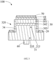
- FIG. 3 is a cross-sectional view taken along line of FIG. 1 .
- FIG. 4 is a plan diagram of another embodiment of an LED structure.
- FIG. 5 is a cross-sectional view taken along line V-V of FIG. 4 .
- FIG. 6 is a cross-sectional view of yet another embodiment of an LED structure.
- FIGS. 1 to 3 illustrate a first embodiment of an LED structure 100 comprising a first electrode 10 , a second electrode 20 , and an epitaxial structure 30 .
- the first electrode 10 and the second electrode 20 are arranged on and electrically connected to the epitaxial structure 30 .
- the LED structure 100 is substantially circular.
- the first electrode 10 and the second electrode 20 are arranged on the epitaxial structure 30 through an electrode film 40 , thereby being electrically connected to the epitaxial structure 30 through the electrode film 40 .
- the electrode film 40 can be made of Indium Tin Oxide (ITO).
- ITO Indium Tin Oxide
- the first electrode 10 and the second electrode 20 are directly attached to the epitaxial structure 30 .
- the epitaxial structure 30 is divided into a base area 31 and a structural supporting area 32 which is annular and surrounds the base area 31 .
- the base area 31 is substantially T-shaped along a cross-section passing through a center axis of the LED structure 100 . That is, the base area 31 comprises a bottom portion 310 and a top portion 311 .
- the bottom portion 310 is wider than the top portion 311 .
- the top portion 311 protrudes from a center area of the bottom portion 310 along a single direction, thereby forming a connecting surface 312 at the bottom portion 310 surrounding the top portion 311 .
- the structural supporting area 32 is annular and protrudes from the connecting surface 312 along the same single direction, thereby causing the structural supporting area 32 to surround the top portion 311 .
- a top of the structural supporting area 32 is aligned (e.g., coplanar) with a top of the top portion 311 .
- the structural supporting area 32 defines at least one slot 320 parallel to the center axis of the LED structure 100 .
- the bottom portion 310 seals an end of each slot 320 . That is, the bottom portion 310 forms a bottom of the slot 320 .
- the first electrode 10 is arranged on the top of the top portion 311 .
- the second electrode 20 is arranged at the bottom of the slot 320 and the top of the structural supporting area 32 .
- the second electrode 20 positioned at the top of the structural supporting area 32 forms an electrode contacting region, which is aligned with the first electrode 10 .
- the second electrode 20 arranged at the bottom of the slot 320 (no structural supporting area 32 below) is attached to the bottom portion 310 and forms a current injection region.
- the electrode contacting region and the current injection region of the second electrode 20 have different heights.
- the first electrode 10 and the second electrode 20 are electrically connected to external electrodes (not shown) through metal bonding, and the epitaxial structure 30 is driven to emit light.
- the structural supporting area 32 defines four slots 320 , which divides the structural supporting area 32 into four portions of equal size. That is, an imaginary line connecting each two opposite slots 320 intersects with the center axis of the LED structure 100 .
- the epitaxial structure 30 has a thickness of about 2 ⁇ m to about 6 ⁇ m. The difference between heights of the electrode contacting region and the current injection region (equal to the depth of each slot 320 ) is about 0.2 ⁇ m to about 2 ⁇ m.
- the imaginary line connecting each two opposite slots 320 does not intersect with the center axis of the LED structure 100 .
- the structural supporting area 32 is spaced apart from the top portion 311 , thereby forming an annular groove 33 between the structural supporting area 32 and the top portion 311 .
- the annular groove 33 communicates with the slot 320 .
- the depth of the annular groove 33 can be equal to the depth of the slot 320 .
- An insulating layer 34 is received in the annular groove 33 and surrounds the periphery of the top portion 311 , thereby obtaining electrical insulation between the first electrode 10 and the second electrode 20 .
- the insulating layer 34 can be made of a material selected from silica (SiO 2 ), silicon nitride (SiN x ), and epoxy resin (for example, SU-8 resin).
- a solder bump 50 is arranged on the top of the first electrode 10 and on the top of the second electrode 20 .
- the epitaxial structure 30 comprises a first semiconductor layer 301 , an active layer 302 , and a second semiconductor layer 303 .
- the second semiconductor layer 303 is positioned at the bottom portion 310 and extends to the top portion 311 and the structural supporting area 32 .
- the first semiconductor layer 301 and the active layer 302 are positioned at the top portion 311 and the structural supporting area 32 .
- the active layer 302 positioned at the top portion 311 is aligned with the active layer 302 positioned at the structural supporting area 32 .
- the first semiconductor layer 301 positioned at the top portion 311 is aligned with the first semiconductor layer 301 positioned at the structural supporting area 32 .
- the first electrode 10 is arranged on the top of the first semiconductor layer 301 positioned at the top portion 311 .
- the second electrode 20 is arranged at the bottom of the slot 320 (that is, attached to the second semiconductor layer 303 ) and on the top of the first semiconductor layer 301 positioned at the structural supporting area 32 .
- the active layer 302 which is surrounded by the insulating layer 34 , emits light.
- the light is emitted out of a surface of the second semiconductor layer 303 facing away from the active layer 302 .
- the light travelling towards the periphery of the epitaxial structure 30 is reflected by the insulating layer 34 and then is emitted out from the surface of the second semiconductor layer 303 facing away from the active layer 302 .
- the first electrode 10 is a P-type electrode.
- the second electrode 20 is an N-type electrode.
- the first semiconductor layer 301 is a P-GaN (P-type Gallium Nitride) layer.
- the active layer 302 is a multiple quantum wells (MQWs) layer.
- the second semiconductor layer 303 is an N-GaN (N-type Gallium Nitride) layer.
- the first electrode 10 and the second electrode 20 can be made of a metal selected from germanium (Ge), nickel (Ni), chromium (Cr), titanium (Ti), tungsten (W), gold (Au), and any combination thereof.
- the LED structure 100 can further comprise a supporting portion 60 .
- the supporting portion 60 is arranged on the surface of the second semiconductor layer 303 facing away from the active layer 302 .
- the supporting portion 60 can be made of plastic material, photo-resist material, SiO 2 , SiN x , or quantum dots (QDs).
- the LED structure 100 can further comprise a protection layer (not shown).
- the protection layer surrounds the periphery of the epitaxial structure 30 to protect the epitaxial structure 30 .
- the protection layer can be a transparent and thermally conductive material.
- FIGS. 4 and 5 illustrate a second embodiment of an LED structure 200 .
- the LED structure 200 is substantially square.
- the structural supporting area 32 does not surround the top portion 311 , but is positioned at a side of the top portion 311 .
- the top of the structural supporting area 32 is aligned with the top of the top portion 311 .
- the second electrode 20 is arranged on the top and at the periphery of the structural supporting area 32 .
- the second electrode 20 arranged at the top of the structural supporting area 32 forms the electrode contacting region.
- the second electrode 20 arranged at the periphery of the structural supporting area 32 surrounds the first semiconductor layer 301 , the active layer 302 , and the second semiconductor layer 303 , and is attached to the bottom portion 310 and forms the current injection region.
- FIG. 6 illustrates a third embodiment of an LED structure 300 .
- the structural supporting area 32 of the LED structure 300 defines a recess 321 .
- the recess 321 extends from the first semiconductor layer 301 to the active layer 302 and the second semiconductor layer 303 .
- the second electrode 20 is arranged on the top of the structural supporting area 32 beside the recess 321 and fills in the recess 321 .
- the second electrode 20 arranged at the top of the structural supporting area 32 forms the electrode contacting region.
- the second electrode 20 filling in the recess 321 is attached to the bottom portion 310 and forms the current injection region.
- the top of the structural supporting area 32 is aligned with the top of the top portion 311 .
- the first electrode 10 arranged on the top portion 311 can be aligned with the second electrode 20 arranged on the structural supporting area 32 . That is, the structural supporting area 32 can block up the periphery of the second semiconductor layer 303 to avoid a height difference between the first electrode 10 and the second electrode 20 .
- an optimal contact during metal bonding can be achieved.
- only a portion of the second electrode 20 is attached to the bottom portion 310 to form the current injection region. The current injection region and the electrode contacting region have different heights.
- the LED structures 100 - 300 have an improved mechanical strength.
Landscapes
- Engineering & Computer Science (AREA)
- Microelectronics & Electronic Packaging (AREA)
- Manufacturing & Machinery (AREA)
- Computer Hardware Design (AREA)
- Power Engineering (AREA)
- Led Devices (AREA)
Abstract
Description
Claims (8)
Priority Applications (2)
| Application Number | Priority Date | Filing Date | Title |
|---|---|---|---|
| US16/290,625 US10873006B2 (en) | 2017-09-30 | 2019-03-01 | Light emitting diode structure |
| US16/950,715 US20210074884A1 (en) | 2017-09-30 | 2020-11-17 | Light emitting diode structure |
Applications Claiming Priority (5)
| Application Number | Priority Date | Filing Date | Title |
|---|---|---|---|
| CN201710915276.6 | 2017-09-30 | ||
| CN201710915276 | 2017-09-30 | ||
| CN201710915276.6A CN109599465A (en) | 2017-09-30 | 2017-09-30 | LED chip construction |
| US15/785,507 US10263148B1 (en) | 2017-09-30 | 2017-10-17 | Light emitting diode structure |
| US16/290,625 US10873006B2 (en) | 2017-09-30 | 2019-03-01 | Light emitting diode structure |
Related Parent Applications (1)
| Application Number | Title | Priority Date | Filing Date |
|---|---|---|---|
| US15/785,507 Division US10263148B1 (en) | 2017-09-30 | 2017-10-17 | Light emitting diode structure |
Related Child Applications (1)
| Application Number | Title | Priority Date | Filing Date |
|---|---|---|---|
| US16/950,715 Division US20210074884A1 (en) | 2017-09-30 | 2020-11-17 | Light emitting diode structure |
Publications (2)
| Publication Number | Publication Date |
|---|---|
| US20190198712A1 US20190198712A1 (en) | 2019-06-27 |
| US10873006B2 true US10873006B2 (en) | 2020-12-22 |
Family
ID=65897558
Family Applications (3)
| Application Number | Title | Priority Date | Filing Date |
|---|---|---|---|
| US15/785,507 Active US10263148B1 (en) | 2017-09-30 | 2017-10-17 | Light emitting diode structure |
| US16/290,625 Active US10873006B2 (en) | 2017-09-30 | 2019-03-01 | Light emitting diode structure |
| US16/950,715 Abandoned US20210074884A1 (en) | 2017-09-30 | 2020-11-17 | Light emitting diode structure |
Family Applications Before (1)
| Application Number | Title | Priority Date | Filing Date |
|---|---|---|---|
| US15/785,507 Active US10263148B1 (en) | 2017-09-30 | 2017-10-17 | Light emitting diode structure |
Family Applications After (1)
| Application Number | Title | Priority Date | Filing Date |
|---|---|---|---|
| US16/950,715 Abandoned US20210074884A1 (en) | 2017-09-30 | 2020-11-17 | Light emitting diode structure |
Country Status (3)
| Country | Link |
|---|---|
| US (3) | US10263148B1 (en) |
| CN (1) | CN109599465A (en) |
| TW (1) | TWI670867B (en) |
Families Citing this family (6)
| Publication number | Priority date | Publication date | Assignee | Title |
|---|---|---|---|---|
| KR102147443B1 (en) | 2018-10-25 | 2020-08-28 | 엘지전자 주식회사 | Display device using semiconductor light emitting device and method for manufacturing the same |
| CN111477726A (en) * | 2019-05-08 | 2020-07-31 | 伊乐视有限公司 | Planar surface mount micro L ED for fluid assembly and preparation method thereof |
| CN111725362A (en) * | 2020-05-27 | 2020-09-29 | 南京中电熊猫平板显示科技有限公司 | Manufacturing method of micro light-emitting diode |
| CN113659050B (en) * | 2021-08-17 | 2023-07-04 | 天津三安光电有限公司 | Light-emitting diode and preparation method thereof |
| CN114023855B (en) * | 2021-09-27 | 2023-11-21 | 重庆康佳光电科技有限公司 | Light-emitting diode chip, preparation method thereof and display device |
| TWI834220B (en) * | 2022-07-14 | 2024-03-01 | 晶成半導體股份有限公司 | Optoelectronic semiconductor device |
Citations (11)
| Publication number | Priority date | Publication date | Assignee | Title |
|---|---|---|---|---|
| US20030209722A1 (en) * | 1999-12-22 | 2003-11-13 | Kabushiki Kaisha Toshiba | Light-emitting element and method of fabrication thereof |
| CN1529364A (en) | 2003-10-13 | 2004-09-15 | 光磊科技股份有限公司 | Light-emitting element capable of increasing light-emitting action area |
| US20100230656A1 (en) * | 2009-02-16 | 2010-09-16 | Rfmd (Uk) Limited | Light emitting structure and method of manufacture thereof |
| US20110294242A1 (en) * | 2009-07-20 | 2011-12-01 | Enerlighting Corp. | Flip-chip gan led fabrication method |
| US20140327036A1 (en) * | 2013-05-03 | 2014-11-06 | Advanced Optoelectronic Technology, Inc. | Light emitting diode chip and manufacturing method thereof |
| US20150162376A1 (en) * | 2013-12-06 | 2015-06-11 | Ju Heon YOON | Semiconductor light emitting device and semiconductor light emitting apparatus including the same |
| US20160064613A1 (en) * | 2014-09-02 | 2016-03-03 | Advanced Optoelectronic Technology, Inc. | Light emitting diode and method for manufacturing the same |
| CN105449068A (en) | 2014-07-28 | 2016-03-30 | 无锡华润华晶微电子有限公司 | LED chip and manufacturing method thereof |
| US20160190396A1 (en) * | 2014-12-26 | 2016-06-30 | Lg Innotek Co., Ltd. | Light emitting device, light emitting device array and lighting apparatus including the same |
| US20190067536A1 (en) * | 2017-08-28 | 2019-02-28 | Nichia Corporation | Light-emitting device |
| US10522712B2 (en) * | 2017-01-10 | 2019-12-31 | PlayNitride Inc. | Micro light-emitting diode chip |
Family Cites Families (13)
| Publication number | Priority date | Publication date | Assignee | Title |
|---|---|---|---|---|
| JPH07297447A (en) * | 1994-04-20 | 1995-11-10 | Toyoda Gosei Co Ltd | Group iii nitride semiconductor light emitting element |
| JP2000049415A (en) * | 1998-07-30 | 2000-02-18 | Matsushita Electric Ind Co Ltd | Nitride semiconductor laser element |
| TWI313069B (en) * | 2002-11-08 | 2009-08-01 | Epistar Corporatio | Light emitting diode and method of making the same |
| TWI220578B (en) * | 2003-09-16 | 2004-08-21 | Opto Tech Corp | Light-emitting device capable of increasing light-emitting active region |
| CN1324719C (en) * | 2004-04-01 | 2007-07-04 | 光磊科技股份有限公司 | Led |
| JP4961887B2 (en) * | 2005-09-07 | 2012-06-27 | 豊田合成株式会社 | Solid state device |
| TWI291246B (en) * | 2005-10-20 | 2007-12-11 | Epistar Corp | Light emitting device and method of forming the same |
| TWI475716B (en) * | 2007-03-19 | 2015-03-01 | Epistar Corp | Optoelectric device |
| CN101276871B (en) * | 2007-03-29 | 2012-08-29 | 晶元光电股份有限公司 | Photovoltaic element, backlight module apparatus and illumination device |
| US9269878B2 (en) * | 2011-05-27 | 2016-02-23 | Lg Innotek Co., Ltd. | Light emitting device and light emitting apparatus |
| CN102403425A (en) * | 2011-11-25 | 2012-04-04 | 俞国宏 | Method for manufacturing inverted LED chip |
| CN104300056B (en) * | 2014-10-11 | 2017-07-07 | 广东晶科电子股份有限公司 | A kind of preparation method of the flip LED chips of high reliability, LED component and LED chip |
| CN105720156B (en) * | 2016-02-03 | 2018-07-31 | 华灿光电(苏州)有限公司 | A kind of light emitting diode and preparation method thereof |
-
2017
- 2017-09-30 CN CN201710915276.6A patent/CN109599465A/en active Pending
- 2017-10-10 TW TW106134623A patent/TWI670867B/en active
- 2017-10-17 US US15/785,507 patent/US10263148B1/en active Active
-
2019
- 2019-03-01 US US16/290,625 patent/US10873006B2/en active Active
-
2020
- 2020-11-17 US US16/950,715 patent/US20210074884A1/en not_active Abandoned
Patent Citations (11)
| Publication number | Priority date | Publication date | Assignee | Title |
|---|---|---|---|---|
| US20030209722A1 (en) * | 1999-12-22 | 2003-11-13 | Kabushiki Kaisha Toshiba | Light-emitting element and method of fabrication thereof |
| CN1529364A (en) | 2003-10-13 | 2004-09-15 | 光磊科技股份有限公司 | Light-emitting element capable of increasing light-emitting action area |
| US20100230656A1 (en) * | 2009-02-16 | 2010-09-16 | Rfmd (Uk) Limited | Light emitting structure and method of manufacture thereof |
| US20110294242A1 (en) * | 2009-07-20 | 2011-12-01 | Enerlighting Corp. | Flip-chip gan led fabrication method |
| US20140327036A1 (en) * | 2013-05-03 | 2014-11-06 | Advanced Optoelectronic Technology, Inc. | Light emitting diode chip and manufacturing method thereof |
| US20150162376A1 (en) * | 2013-12-06 | 2015-06-11 | Ju Heon YOON | Semiconductor light emitting device and semiconductor light emitting apparatus including the same |
| CN105449068A (en) | 2014-07-28 | 2016-03-30 | 无锡华润华晶微电子有限公司 | LED chip and manufacturing method thereof |
| US20160064613A1 (en) * | 2014-09-02 | 2016-03-03 | Advanced Optoelectronic Technology, Inc. | Light emitting diode and method for manufacturing the same |
| US20160190396A1 (en) * | 2014-12-26 | 2016-06-30 | Lg Innotek Co., Ltd. | Light emitting device, light emitting device array and lighting apparatus including the same |
| US10522712B2 (en) * | 2017-01-10 | 2019-12-31 | PlayNitride Inc. | Micro light-emitting diode chip |
| US20190067536A1 (en) * | 2017-08-28 | 2019-02-28 | Nichia Corporation | Light-emitting device |
Also Published As
| Publication number | Publication date |
|---|---|
| CN109599465A (en) | 2019-04-09 |
| US20190198712A1 (en) | 2019-06-27 |
| TW201916404A (en) | 2019-04-16 |
| TWI670867B (en) | 2019-09-01 |
| US20210074884A1 (en) | 2021-03-11 |
| US20190103512A1 (en) | 2019-04-04 |
| US10263148B1 (en) | 2019-04-16 |
Similar Documents
| Publication | Publication Date | Title |
|---|---|---|
| US10873006B2 (en) | Light emitting diode structure | |
| US20230197892A1 (en) | Display device using semiconductor light emitting diode | |
| US11563149B2 (en) | Light-emitting device | |
| US8987761B2 (en) | Light-emitting device | |
| US10790415B2 (en) | Semiconductor light-emitting device | |
| US11393967B2 (en) | Eutectic electrode structure of flip-chip LED chip and flip-chip LED chip | |
| US8772793B2 (en) | Light emitting diodes and method for manufacturing the same | |
| TW200824151A (en) | Semiconductor light-emitting device | |
| KR20200139455A (en) | Anodic oxidation for electric contacting and opto electronic display and manufacturing method of opto electronic | |
| JP2014022401A (en) | Nitride semiconductor light-emitting element | |
| CN111052409B (en) | Light emitting diode device and method of manufacturing the same | |
| US10115864B2 (en) | Optoelectronic device with light-emitting diodes and an improved radiation pattern | |
| KR20150107400A (en) | Light emitting diode | |
| US11658259B2 (en) | Light emitting device | |
| JP6067408B2 (en) | Flip-chip type semiconductor light emitting device, semiconductor device and manufacturing method thereof | |
| JP2017054902A (en) | Semiconductor light emitting device | |
| KR102504334B1 (en) | Light emitting device | |
| KR20160059221A (en) | Light emitting device and lighting system | |
| KR20220139690A (en) | Semiconductor light emitting device and light emitting device package having the same | |
| KR20220112157A (en) | Light emitting device and display apparatus including the same | |
| CN111725192A (en) | Method and structure for bonding light emitting diode and substrate |
Legal Events
| Date | Code | Title | Description |
|---|---|---|---|
| AS | Assignment |
Owner name: ADVANCED OPTOELECTRONIC TECHNOLOGY, INC., TAIWAN Free format text: ASSIGNMENT OF ASSIGNORS INTEREST;ASSIGNORS:HUNG, TZU-CHIEN;PENG, CHIEN-CHUNG;HUANG, CHIEN-SHIANG;AND OTHERS;REEL/FRAME:048484/0525 Effective date: 20171013 |
|
| FEPP | Fee payment procedure |
Free format text: ENTITY STATUS SET TO UNDISCOUNTED (ORIGINAL EVENT CODE: BIG.); ENTITY STATUS OF PATENT OWNER: LARGE ENTITY |
|
| STPP | Information on status: patent application and granting procedure in general |
Free format text: NON FINAL ACTION MAILED |
|
| STPP | Information on status: patent application and granting procedure in general |
Free format text: RESPONSE TO NON-FINAL OFFICE ACTION ENTERED AND FORWARDED TO EXAMINER |
|
| STPP | Information on status: patent application and granting procedure in general |
Free format text: RESPONSE TO NON-FINAL OFFICE ACTION ENTERED AND FORWARDED TO EXAMINER |
|
| STPP | Information on status: patent application and granting procedure in general |
Free format text: NOTICE OF ALLOWANCE MAILED -- APPLICATION RECEIVED IN OFFICE OF PUBLICATIONS |
|
| STPP | Information on status: patent application and granting procedure in general |
Free format text: PUBLICATIONS -- ISSUE FEE PAYMENT VERIFIED |
|
| STCF | Information on status: patent grant |
Free format text: PATENTED CASE |
|
| MAFP | Maintenance fee payment |
Free format text: PAYMENT OF MAINTENANCE FEE, 4TH YEAR, LARGE ENTITY (ORIGINAL EVENT CODE: M1551); ENTITY STATUS OF PATENT OWNER: LARGE ENTITY Year of fee payment: 4 |