US10868217B2 - LED chips, method of manufacturing the same, and display panels - Google Patents
LED chips, method of manufacturing the same, and display panels Download PDFInfo
- Publication number
- US10868217B2 US10868217B2 US16/416,298 US201916416298A US10868217B2 US 10868217 B2 US10868217 B2 US 10868217B2 US 201916416298 A US201916416298 A US 201916416298A US 10868217 B2 US10868217 B2 US 10868217B2
- Authority
- US
- United States
- Prior art keywords
- electrode
- contact electrode
- extension electrode
- extension
- layer
- Prior art date
- Legal status (The legal status is an assumption and is not a legal conclusion. Google has not performed a legal analysis and makes no representation as to the accuracy of the status listed.)
- Active
Links
Images


Classifications
-
- H—ELECTRICITY
- H01—ELECTRIC ELEMENTS
- H01L—SEMICONDUCTOR DEVICES NOT COVERED BY CLASS H10
- H01L24/00—Arrangements for connecting or disconnecting semiconductor or solid-state bodies; Methods or apparatus related thereto
- H01L24/01—Means for bonding being attached to, or being formed on, the surface to be connected, e.g. chip-to-package, die-attach, "first-level" interconnects; Manufacturing methods related thereto
- H01L24/02—Bonding areas ; Manufacturing methods related thereto
- H01L24/04—Structure, shape, material or disposition of the bonding areas prior to the connecting process
- H01L24/05—Structure, shape, material or disposition of the bonding areas prior to the connecting process of an individual bonding area
-
- H—ELECTRICITY
- H01—ELECTRIC ELEMENTS
- H01L—SEMICONDUCTOR DEVICES NOT COVERED BY CLASS H10
- H01L33/00—Semiconductor devices with at least one potential-jump barrier or surface barrier specially adapted for light emission; Processes or apparatus specially adapted for the manufacture or treatment thereof or of parts thereof; Details thereof
- H01L33/36—Semiconductor devices with at least one potential-jump barrier or surface barrier specially adapted for light emission; Processes or apparatus specially adapted for the manufacture or treatment thereof or of parts thereof; Details thereof characterised by the electrodes
- H01L33/38—Semiconductor devices with at least one potential-jump barrier or surface barrier specially adapted for light emission; Processes or apparatus specially adapted for the manufacture or treatment thereof or of parts thereof; Details thereof characterised by the electrodes with a particular shape
-
- G—PHYSICS
- G09—EDUCATION; CRYPTOGRAPHY; DISPLAY; ADVERTISING; SEALS
- G09G—ARRANGEMENTS OR CIRCUITS FOR CONTROL OF INDICATING DEVICES USING STATIC MEANS TO PRESENT VARIABLE INFORMATION
- G09G3/00—Control arrangements or circuits, of interest only in connection with visual indicators other than cathode-ray tubes
- G09G3/20—Control arrangements or circuits, of interest only in connection with visual indicators other than cathode-ray tubes for presentation of an assembly of a number of characters, e.g. a page, by composing the assembly by combination of individual elements arranged in a matrix no fixed position being assigned to or needed to be assigned to the individual characters or partial characters
- G09G3/22—Control arrangements or circuits, of interest only in connection with visual indicators other than cathode-ray tubes for presentation of an assembly of a number of characters, e.g. a page, by composing the assembly by combination of individual elements arranged in a matrix no fixed position being assigned to or needed to be assigned to the individual characters or partial characters using controlled light sources
- G09G3/30—Control arrangements or circuits, of interest only in connection with visual indicators other than cathode-ray tubes for presentation of an assembly of a number of characters, e.g. a page, by composing the assembly by combination of individual elements arranged in a matrix no fixed position being assigned to or needed to be assigned to the individual characters or partial characters using controlled light sources using electroluminescent panels
- G09G3/32—Control arrangements or circuits, of interest only in connection with visual indicators other than cathode-ray tubes for presentation of an assembly of a number of characters, e.g. a page, by composing the assembly by combination of individual elements arranged in a matrix no fixed position being assigned to or needed to be assigned to the individual characters or partial characters using controlled light sources using electroluminescent panels semiconductive, e.g. using light-emitting diodes [LED]
-
- H—ELECTRICITY
- H01—ELECTRIC ELEMENTS
- H01L—SEMICONDUCTOR DEVICES NOT COVERED BY CLASS H10
- H01L24/00—Arrangements for connecting or disconnecting semiconductor or solid-state bodies; Methods or apparatus related thereto
- H01L24/01—Means for bonding being attached to, or being formed on, the surface to be connected, e.g. chip-to-package, die-attach, "first-level" interconnects; Manufacturing methods related thereto
- H01L24/02—Bonding areas ; Manufacturing methods related thereto
- H01L24/03—Manufacturing methods
-
- H—ELECTRICITY
- H01—ELECTRIC ELEMENTS
- H01L—SEMICONDUCTOR DEVICES NOT COVERED BY CLASS H10
- H01L24/00—Arrangements for connecting or disconnecting semiconductor or solid-state bodies; Methods or apparatus related thereto
- H01L24/01—Means for bonding being attached to, or being formed on, the surface to be connected, e.g. chip-to-package, die-attach, "first-level" interconnects; Manufacturing methods related thereto
- H01L24/02—Bonding areas ; Manufacturing methods related thereto
- H01L24/04—Structure, shape, material or disposition of the bonding areas prior to the connecting process
- H01L24/06—Structure, shape, material or disposition of the bonding areas prior to the connecting process of a plurality of bonding areas
-
- H—ELECTRICITY
- H01—ELECTRIC ELEMENTS
- H01L—SEMICONDUCTOR DEVICES NOT COVERED BY CLASS H10
- H01L24/00—Arrangements for connecting or disconnecting semiconductor or solid-state bodies; Methods or apparatus related thereto
- H01L24/01—Means for bonding being attached to, or being formed on, the surface to be connected, e.g. chip-to-package, die-attach, "first-level" interconnects; Manufacturing methods related thereto
- H01L24/26—Layer connectors, e.g. plate connectors, solder or adhesive layers; Manufacturing methods related thereto
- H01L24/28—Structure, shape, material or disposition of the layer connectors prior to the connecting process
-
- H—ELECTRICITY
- H01—ELECTRIC ELEMENTS
- H01L—SEMICONDUCTOR DEVICES NOT COVERED BY CLASS H10
- H01L33/00—Semiconductor devices with at least one potential-jump barrier or surface barrier specially adapted for light emission; Processes or apparatus specially adapted for the manufacture or treatment thereof or of parts thereof; Details thereof
- H01L33/0004—Devices characterised by their operation
- H01L33/0008—Devices characterised by their operation having p-n or hi-lo junctions
- H01L33/0016—Devices characterised by their operation having p-n or hi-lo junctions having at least two p-n junctions
-
- H—ELECTRICITY
- H01—ELECTRIC ELEMENTS
- H01L—SEMICONDUCTOR DEVICES NOT COVERED BY CLASS H10
- H01L33/00—Semiconductor devices with at least one potential-jump barrier or surface barrier specially adapted for light emission; Processes or apparatus specially adapted for the manufacture or treatment thereof or of parts thereof; Details thereof
- H01L33/36—Semiconductor devices with at least one potential-jump barrier or surface barrier specially adapted for light emission; Processes or apparatus specially adapted for the manufacture or treatment thereof or of parts thereof; Details thereof characterised by the electrodes
- H01L33/38—Semiconductor devices with at least one potential-jump barrier or surface barrier specially adapted for light emission; Processes or apparatus specially adapted for the manufacture or treatment thereof or of parts thereof; Details thereof characterised by the electrodes with a particular shape
- H01L33/387—Semiconductor devices with at least one potential-jump barrier or surface barrier specially adapted for light emission; Processes or apparatus specially adapted for the manufacture or treatment thereof or of parts thereof; Details thereof characterised by the electrodes with a particular shape with a plurality of electrode regions in direct contact with the semiconductor body and being electrically interconnected by another electrode layer
-
- H—ELECTRICITY
- H01—ELECTRIC ELEMENTS
- H01L—SEMICONDUCTOR DEVICES NOT COVERED BY CLASS H10
- H01L2224/00—Indexing scheme for arrangements for connecting or disconnecting semiconductor or solid-state bodies and methods related thereto as covered by H01L24/00
- H01L2224/01—Means for bonding being attached to, or being formed on, the surface to be connected, e.g. chip-to-package, die-attach, "first-level" interconnects; Manufacturing methods related thereto
- H01L2224/02—Bonding areas; Manufacturing methods related thereto
- H01L2224/023—Redistribution layers [RDL] for bonding areas
- H01L2224/0239—Material of the redistribution layers
-
- H—ELECTRICITY
- H01—ELECTRIC ELEMENTS
- H01L—SEMICONDUCTOR DEVICES NOT COVERED BY CLASS H10
- H01L2224/00—Indexing scheme for arrangements for connecting or disconnecting semiconductor or solid-state bodies and methods related thereto as covered by H01L24/00
- H01L2224/01—Means for bonding being attached to, or being formed on, the surface to be connected, e.g. chip-to-package, die-attach, "first-level" interconnects; Manufacturing methods related thereto
- H01L2224/02—Bonding areas; Manufacturing methods related thereto
- H01L2224/03—Manufacturing methods
- H01L2224/034—Manufacturing methods by blanket deposition of the material of the bonding area
- H01L2224/03444—Manufacturing methods by blanket deposition of the material of the bonding area in gaseous form
- H01L2224/0345—Physical vapour deposition [PVD], e.g. evaporation, or sputtering
-
- H—ELECTRICITY
- H01—ELECTRIC ELEMENTS
- H01L—SEMICONDUCTOR DEVICES NOT COVERED BY CLASS H10
- H01L2224/00—Indexing scheme for arrangements for connecting or disconnecting semiconductor or solid-state bodies and methods related thereto as covered by H01L24/00
- H01L2224/01—Means for bonding being attached to, or being formed on, the surface to be connected, e.g. chip-to-package, die-attach, "first-level" interconnects; Manufacturing methods related thereto
- H01L2224/02—Bonding areas; Manufacturing methods related thereto
- H01L2224/03—Manufacturing methods
- H01L2224/034—Manufacturing methods by blanket deposition of the material of the bonding area
- H01L2224/0346—Plating
- H01L2224/03462—Electroplating
-
- H—ELECTRICITY
- H01—ELECTRIC ELEMENTS
- H01L—SEMICONDUCTOR DEVICES NOT COVERED BY CLASS H10
- H01L2224/00—Indexing scheme for arrangements for connecting or disconnecting semiconductor or solid-state bodies and methods related thereto as covered by H01L24/00
- H01L2224/01—Means for bonding being attached to, or being formed on, the surface to be connected, e.g. chip-to-package, die-attach, "first-level" interconnects; Manufacturing methods related thereto
- H01L2224/02—Bonding areas; Manufacturing methods related thereto
- H01L2224/03—Manufacturing methods
- H01L2224/0347—Manufacturing methods using a lift-off mask
-
- H—ELECTRICITY
- H01—ELECTRIC ELEMENTS
- H01L—SEMICONDUCTOR DEVICES NOT COVERED BY CLASS H10
- H01L2224/00—Indexing scheme for arrangements for connecting or disconnecting semiconductor or solid-state bodies and methods related thereto as covered by H01L24/00
- H01L2224/01—Means for bonding being attached to, or being formed on, the surface to be connected, e.g. chip-to-package, die-attach, "first-level" interconnects; Manufacturing methods related thereto
- H01L2224/02—Bonding areas; Manufacturing methods related thereto
- H01L2224/03—Manufacturing methods
- H01L2224/036—Manufacturing methods by patterning a pre-deposited material
- H01L2224/03618—Manufacturing methods by patterning a pre-deposited material with selective exposure, development and removal of a photosensitive material, e.g. of a photosensitive conductive resin
- H01L2224/0362—Photolithography
-
- H—ELECTRICITY
- H01—ELECTRIC ELEMENTS
- H01L—SEMICONDUCTOR DEVICES NOT COVERED BY CLASS H10
- H01L2224/00—Indexing scheme for arrangements for connecting or disconnecting semiconductor or solid-state bodies and methods related thereto as covered by H01L24/00
- H01L2224/01—Means for bonding being attached to, or being formed on, the surface to be connected, e.g. chip-to-package, die-attach, "first-level" interconnects; Manufacturing methods related thereto
- H01L2224/02—Bonding areas; Manufacturing methods related thereto
- H01L2224/04—Structure, shape, material or disposition of the bonding areas prior to the connecting process
- H01L2224/04026—Bonding areas specifically adapted for layer connectors
-
- H—ELECTRICITY
- H01—ELECTRIC ELEMENTS
- H01L—SEMICONDUCTOR DEVICES NOT COVERED BY CLASS H10
- H01L2224/00—Indexing scheme for arrangements for connecting or disconnecting semiconductor or solid-state bodies and methods related thereto as covered by H01L24/00
- H01L2224/01—Means for bonding being attached to, or being formed on, the surface to be connected, e.g. chip-to-package, die-attach, "first-level" interconnects; Manufacturing methods related thereto
- H01L2224/02—Bonding areas; Manufacturing methods related thereto
- H01L2224/04—Structure, shape, material or disposition of the bonding areas prior to the connecting process
- H01L2224/05—Structure, shape, material or disposition of the bonding areas prior to the connecting process of an individual bonding area
- H01L2224/05001—Internal layers
- H01L2224/05005—Structure
- H01L2224/05008—Bonding area integrally formed with a redistribution layer on the semiconductor or solid-state body, e.g.
-
- H—ELECTRICITY
- H01—ELECTRIC ELEMENTS
- H01L—SEMICONDUCTOR DEVICES NOT COVERED BY CLASS H10
- H01L2224/00—Indexing scheme for arrangements for connecting or disconnecting semiconductor or solid-state bodies and methods related thereto as covered by H01L24/00
- H01L2224/01—Means for bonding being attached to, or being formed on, the surface to be connected, e.g. chip-to-package, die-attach, "first-level" interconnects; Manufacturing methods related thereto
- H01L2224/02—Bonding areas; Manufacturing methods related thereto
- H01L2224/04—Structure, shape, material or disposition of the bonding areas prior to the connecting process
- H01L2224/05—Structure, shape, material or disposition of the bonding areas prior to the connecting process of an individual bonding area
- H01L2224/05001—Internal layers
- H01L2224/0501—Shape
- H01L2224/05012—Shape in top view
- H01L2224/05013—Shape in top view being rectangular
-
- H—ELECTRICITY
- H01—ELECTRIC ELEMENTS
- H01L—SEMICONDUCTOR DEVICES NOT COVERED BY CLASS H10
- H01L2224/00—Indexing scheme for arrangements for connecting or disconnecting semiconductor or solid-state bodies and methods related thereto as covered by H01L24/00
- H01L2224/01—Means for bonding being attached to, or being formed on, the surface to be connected, e.g. chip-to-package, die-attach, "first-level" interconnects; Manufacturing methods related thereto
- H01L2224/02—Bonding areas; Manufacturing methods related thereto
- H01L2224/04—Structure, shape, material or disposition of the bonding areas prior to the connecting process
- H01L2224/05—Structure, shape, material or disposition of the bonding areas prior to the connecting process of an individual bonding area
- H01L2224/05001—Internal layers
- H01L2224/0501—Shape
- H01L2224/05012—Shape in top view
- H01L2224/05014—Shape in top view being square
-
- H—ELECTRICITY
- H01—ELECTRIC ELEMENTS
- H01L—SEMICONDUCTOR DEVICES NOT COVERED BY CLASS H10
- H01L2224/00—Indexing scheme for arrangements for connecting or disconnecting semiconductor or solid-state bodies and methods related thereto as covered by H01L24/00
- H01L2224/01—Means for bonding being attached to, or being formed on, the surface to be connected, e.g. chip-to-package, die-attach, "first-level" interconnects; Manufacturing methods related thereto
- H01L2224/02—Bonding areas; Manufacturing methods related thereto
- H01L2224/04—Structure, shape, material or disposition of the bonding areas prior to the connecting process
- H01L2224/05—Structure, shape, material or disposition of the bonding areas prior to the connecting process of an individual bonding area
- H01L2224/05001—Internal layers
- H01L2224/0501—Shape
- H01L2224/05012—Shape in top view
- H01L2224/05015—Shape in top view being circular or elliptic
-
- H—ELECTRICITY
- H01—ELECTRIC ELEMENTS
- H01L—SEMICONDUCTOR DEVICES NOT COVERED BY CLASS H10
- H01L2224/00—Indexing scheme for arrangements for connecting or disconnecting semiconductor or solid-state bodies and methods related thereto as covered by H01L24/00
- H01L2224/01—Means for bonding being attached to, or being formed on, the surface to be connected, e.g. chip-to-package, die-attach, "first-level" interconnects; Manufacturing methods related thereto
- H01L2224/02—Bonding areas; Manufacturing methods related thereto
- H01L2224/04—Structure, shape, material or disposition of the bonding areas prior to the connecting process
- H01L2224/05—Structure, shape, material or disposition of the bonding areas prior to the connecting process of an individual bonding area
- H01L2224/05001—Internal layers
- H01L2224/0502—Disposition
- H01L2224/05022—Disposition the internal layer being at least partially embedded in the surface
-
- H—ELECTRICITY
- H01—ELECTRIC ELEMENTS
- H01L—SEMICONDUCTOR DEVICES NOT COVERED BY CLASS H10
- H01L2224/00—Indexing scheme for arrangements for connecting or disconnecting semiconductor or solid-state bodies and methods related thereto as covered by H01L24/00
- H01L2224/01—Means for bonding being attached to, or being formed on, the surface to be connected, e.g. chip-to-package, die-attach, "first-level" interconnects; Manufacturing methods related thereto
- H01L2224/02—Bonding areas; Manufacturing methods related thereto
- H01L2224/04—Structure, shape, material or disposition of the bonding areas prior to the connecting process
- H01L2224/05—Structure, shape, material or disposition of the bonding areas prior to the connecting process of an individual bonding area
- H01L2224/05001—Internal layers
- H01L2224/05099—Material
- H01L2224/051—Material with a principal constituent of the material being a metal or a metalloid, e.g. boron [B], silicon [Si], germanium [Ge], arsenic [As], antimony [Sb], tellurium [Te] and polonium [Po], and alloys thereof
-
- H—ELECTRICITY
- H01—ELECTRIC ELEMENTS
- H01L—SEMICONDUCTOR DEVICES NOT COVERED BY CLASS H10
- H01L2224/00—Indexing scheme for arrangements for connecting or disconnecting semiconductor or solid-state bodies and methods related thereto as covered by H01L24/00
- H01L2224/01—Means for bonding being attached to, or being formed on, the surface to be connected, e.g. chip-to-package, die-attach, "first-level" interconnects; Manufacturing methods related thereto
- H01L2224/02—Bonding areas; Manufacturing methods related thereto
- H01L2224/04—Structure, shape, material or disposition of the bonding areas prior to the connecting process
- H01L2224/05—Structure, shape, material or disposition of the bonding areas prior to the connecting process of an individual bonding area
- H01L2224/0554—External layer
- H01L2224/05541—Structure
- H01L2224/05548—Bonding area integrally formed with a redistribution layer on the semiconductor or solid-state body
-
- H—ELECTRICITY
- H01—ELECTRIC ELEMENTS
- H01L—SEMICONDUCTOR DEVICES NOT COVERED BY CLASS H10
- H01L2224/00—Indexing scheme for arrangements for connecting or disconnecting semiconductor or solid-state bodies and methods related thereto as covered by H01L24/00
- H01L2224/01—Means for bonding being attached to, or being formed on, the surface to be connected, e.g. chip-to-package, die-attach, "first-level" interconnects; Manufacturing methods related thereto
- H01L2224/02—Bonding areas; Manufacturing methods related thereto
- H01L2224/04—Structure, shape, material or disposition of the bonding areas prior to the connecting process
- H01L2224/05—Structure, shape, material or disposition of the bonding areas prior to the connecting process of an individual bonding area
- H01L2224/0554—External layer
- H01L2224/0555—Shape
- H01L2224/05551—Shape comprising apertures or cavities
-
- H—ELECTRICITY
- H01—ELECTRIC ELEMENTS
- H01L—SEMICONDUCTOR DEVICES NOT COVERED BY CLASS H10
- H01L2224/00—Indexing scheme for arrangements for connecting or disconnecting semiconductor or solid-state bodies and methods related thereto as covered by H01L24/00
- H01L2224/01—Means for bonding being attached to, or being formed on, the surface to be connected, e.g. chip-to-package, die-attach, "first-level" interconnects; Manufacturing methods related thereto
- H01L2224/02—Bonding areas; Manufacturing methods related thereto
- H01L2224/04—Structure, shape, material or disposition of the bonding areas prior to the connecting process
- H01L2224/05—Structure, shape, material or disposition of the bonding areas prior to the connecting process of an individual bonding area
- H01L2224/0554—External layer
- H01L2224/0555—Shape
- H01L2224/05552—Shape in top view
- H01L2224/05555—Shape in top view being circular or elliptic
-
- H—ELECTRICITY
- H01—ELECTRIC ELEMENTS
- H01L—SEMICONDUCTOR DEVICES NOT COVERED BY CLASS H10
- H01L2224/00—Indexing scheme for arrangements for connecting or disconnecting semiconductor or solid-state bodies and methods related thereto as covered by H01L24/00
- H01L2224/01—Means for bonding being attached to, or being formed on, the surface to be connected, e.g. chip-to-package, die-attach, "first-level" interconnects; Manufacturing methods related thereto
- H01L2224/02—Bonding areas; Manufacturing methods related thereto
- H01L2224/04—Structure, shape, material or disposition of the bonding areas prior to the connecting process
- H01L2224/05—Structure, shape, material or disposition of the bonding areas prior to the connecting process of an individual bonding area
- H01L2224/0554—External layer
- H01L2224/0556—Disposition
- H01L2224/05563—Only on parts of the surface of the internal layer
- H01L2224/05564—Only on the bonding interface of the bonding area
-
- H—ELECTRICITY
- H01—ELECTRIC ELEMENTS
- H01L—SEMICONDUCTOR DEVICES NOT COVERED BY CLASS H10
- H01L2224/00—Indexing scheme for arrangements for connecting or disconnecting semiconductor or solid-state bodies and methods related thereto as covered by H01L24/00
- H01L2224/01—Means for bonding being attached to, or being formed on, the surface to be connected, e.g. chip-to-package, die-attach, "first-level" interconnects; Manufacturing methods related thereto
- H01L2224/02—Bonding areas; Manufacturing methods related thereto
- H01L2224/04—Structure, shape, material or disposition of the bonding areas prior to the connecting process
- H01L2224/05—Structure, shape, material or disposition of the bonding areas prior to the connecting process of an individual bonding area
- H01L2224/0554—External layer
- H01L2224/0556—Disposition
- H01L2224/05567—Disposition the external layer being at least partially embedded in the surface
-
- H—ELECTRICITY
- H01—ELECTRIC ELEMENTS
- H01L—SEMICONDUCTOR DEVICES NOT COVERED BY CLASS H10
- H01L2224/00—Indexing scheme for arrangements for connecting or disconnecting semiconductor or solid-state bodies and methods related thereto as covered by H01L24/00
- H01L2224/01—Means for bonding being attached to, or being formed on, the surface to be connected, e.g. chip-to-package, die-attach, "first-level" interconnects; Manufacturing methods related thereto
- H01L2224/02—Bonding areas; Manufacturing methods related thereto
- H01L2224/04—Structure, shape, material or disposition of the bonding areas prior to the connecting process
- H01L2224/05—Structure, shape, material or disposition of the bonding areas prior to the connecting process of an individual bonding area
- H01L2224/0554—External layer
- H01L2224/0556—Disposition
- H01L2224/05568—Disposition the whole external layer protruding from the surface
-
- H—ELECTRICITY
- H01—ELECTRIC ELEMENTS
- H01L—SEMICONDUCTOR DEVICES NOT COVERED BY CLASS H10
- H01L2224/00—Indexing scheme for arrangements for connecting or disconnecting semiconductor or solid-state bodies and methods related thereto as covered by H01L24/00
- H01L2224/01—Means for bonding being attached to, or being formed on, the surface to be connected, e.g. chip-to-package, die-attach, "first-level" interconnects; Manufacturing methods related thereto
- H01L2224/02—Bonding areas; Manufacturing methods related thereto
- H01L2224/04—Structure, shape, material or disposition of the bonding areas prior to the connecting process
- H01L2224/05—Structure, shape, material or disposition of the bonding areas prior to the connecting process of an individual bonding area
- H01L2224/0554—External layer
- H01L2224/05599—Material
- H01L2224/056—Material with a principal constituent of the material being a metal or a metalloid, e.g. boron [B], silicon [Si], germanium [Ge], arsenic [As], antimony [Sb], tellurium [Te] and polonium [Po], and alloys thereof
- H01L2224/05617—Material with a principal constituent of the material being a metal or a metalloid, e.g. boron [B], silicon [Si], germanium [Ge], arsenic [As], antimony [Sb], tellurium [Te] and polonium [Po], and alloys thereof the principal constituent melting at a temperature of greater than or equal to 400°C and less than 950°C
- H01L2224/05624—Aluminium [Al] as principal constituent
-
- H—ELECTRICITY
- H01—ELECTRIC ELEMENTS
- H01L—SEMICONDUCTOR DEVICES NOT COVERED BY CLASS H10
- H01L2224/00—Indexing scheme for arrangements for connecting or disconnecting semiconductor or solid-state bodies and methods related thereto as covered by H01L24/00
- H01L2224/01—Means for bonding being attached to, or being formed on, the surface to be connected, e.g. chip-to-package, die-attach, "first-level" interconnects; Manufacturing methods related thereto
- H01L2224/02—Bonding areas; Manufacturing methods related thereto
- H01L2224/04—Structure, shape, material or disposition of the bonding areas prior to the connecting process
- H01L2224/05—Structure, shape, material or disposition of the bonding areas prior to the connecting process of an individual bonding area
- H01L2224/0554—External layer
- H01L2224/05599—Material
- H01L2224/056—Material with a principal constituent of the material being a metal or a metalloid, e.g. boron [B], silicon [Si], germanium [Ge], arsenic [As], antimony [Sb], tellurium [Te] and polonium [Po], and alloys thereof
- H01L2224/05638—Material with a principal constituent of the material being a metal or a metalloid, e.g. boron [B], silicon [Si], germanium [Ge], arsenic [As], antimony [Sb], tellurium [Te] and polonium [Po], and alloys thereof the principal constituent melting at a temperature of greater than or equal to 950°C and less than 1550°C
- H01L2224/05639—Silver [Ag] as principal constituent
-
- H—ELECTRICITY
- H01—ELECTRIC ELEMENTS
- H01L—SEMICONDUCTOR DEVICES NOT COVERED BY CLASS H10
- H01L2224/00—Indexing scheme for arrangements for connecting or disconnecting semiconductor or solid-state bodies and methods related thereto as covered by H01L24/00
- H01L2224/01—Means for bonding being attached to, or being formed on, the surface to be connected, e.g. chip-to-package, die-attach, "first-level" interconnects; Manufacturing methods related thereto
- H01L2224/02—Bonding areas; Manufacturing methods related thereto
- H01L2224/04—Structure, shape, material or disposition of the bonding areas prior to the connecting process
- H01L2224/05—Structure, shape, material or disposition of the bonding areas prior to the connecting process of an individual bonding area
- H01L2224/0554—External layer
- H01L2224/05599—Material
- H01L2224/056—Material with a principal constituent of the material being a metal or a metalloid, e.g. boron [B], silicon [Si], germanium [Ge], arsenic [As], antimony [Sb], tellurium [Te] and polonium [Po], and alloys thereof
- H01L2224/05638—Material with a principal constituent of the material being a metal or a metalloid, e.g. boron [B], silicon [Si], germanium [Ge], arsenic [As], antimony [Sb], tellurium [Te] and polonium [Po], and alloys thereof the principal constituent melting at a temperature of greater than or equal to 950°C and less than 1550°C
- H01L2224/05644—Gold [Au] as principal constituent
-
- H—ELECTRICITY
- H01—ELECTRIC ELEMENTS
- H01L—SEMICONDUCTOR DEVICES NOT COVERED BY CLASS H10
- H01L2224/00—Indexing scheme for arrangements for connecting or disconnecting semiconductor or solid-state bodies and methods related thereto as covered by H01L24/00
- H01L2224/01—Means for bonding being attached to, or being formed on, the surface to be connected, e.g. chip-to-package, die-attach, "first-level" interconnects; Manufacturing methods related thereto
- H01L2224/02—Bonding areas; Manufacturing methods related thereto
- H01L2224/04—Structure, shape, material or disposition of the bonding areas prior to the connecting process
- H01L2224/06—Structure, shape, material or disposition of the bonding areas prior to the connecting process of a plurality of bonding areas
- H01L2224/0601—Structure
- H01L2224/0603—Bonding areas having different sizes, e.g. different heights or widths
-
- H—ELECTRICITY
- H01—ELECTRIC ELEMENTS
- H01L—SEMICONDUCTOR DEVICES NOT COVERED BY CLASS H10
- H01L2224/00—Indexing scheme for arrangements for connecting or disconnecting semiconductor or solid-state bodies and methods related thereto as covered by H01L24/00
- H01L2224/01—Means for bonding being attached to, or being formed on, the surface to be connected, e.g. chip-to-package, die-attach, "first-level" interconnects; Manufacturing methods related thereto
- H01L2224/02—Bonding areas; Manufacturing methods related thereto
- H01L2224/04—Structure, shape, material or disposition of the bonding areas prior to the connecting process
- H01L2224/06—Structure, shape, material or disposition of the bonding areas prior to the connecting process of a plurality of bonding areas
- H01L2224/061—Disposition
- H01L2224/06102—Disposition the bonding areas being at different heights
-
- H—ELECTRICITY
- H01—ELECTRIC ELEMENTS
- H01L—SEMICONDUCTOR DEVICES NOT COVERED BY CLASS H10
- H01L2224/00—Indexing scheme for arrangements for connecting or disconnecting semiconductor or solid-state bodies and methods related thereto as covered by H01L24/00
- H01L2224/01—Means for bonding being attached to, or being formed on, the surface to be connected, e.g. chip-to-package, die-attach, "first-level" interconnects; Manufacturing methods related thereto
- H01L2224/26—Layer connectors, e.g. plate connectors, solder or adhesive layers; Manufacturing methods related thereto
- H01L2224/2612—Auxiliary members for layer connectors, e.g. spacers
- H01L2224/26122—Auxiliary members for layer connectors, e.g. spacers being formed on the semiconductor or solid-state body to be connected
- H01L2224/26145—Flow barriers
-
- H—ELECTRICITY
- H01—ELECTRIC ELEMENTS
- H01L—SEMICONDUCTOR DEVICES NOT COVERED BY CLASS H10
- H01L2224/00—Indexing scheme for arrangements for connecting or disconnecting semiconductor or solid-state bodies and methods related thereto as covered by H01L24/00
- H01L2224/01—Means for bonding being attached to, or being formed on, the surface to be connected, e.g. chip-to-package, die-attach, "first-level" interconnects; Manufacturing methods related thereto
- H01L2224/26—Layer connectors, e.g. plate connectors, solder or adhesive layers; Manufacturing methods related thereto
- H01L2224/28—Structure, shape, material or disposition of the layer connectors prior to the connecting process
- H01L2224/29—Structure, shape, material or disposition of the layer connectors prior to the connecting process of an individual layer connector
- H01L2224/29001—Core members of the layer connector
- H01L2224/29099—Material
- H01L2224/291—Material with a principal constituent of the material being a metal or a metalloid, e.g. boron [B], silicon [Si], germanium [Ge], arsenic [As], antimony [Sb], tellurium [Te] and polonium [Po], and alloys thereof
-
- H—ELECTRICITY
- H01—ELECTRIC ELEMENTS
- H01L—SEMICONDUCTOR DEVICES NOT COVERED BY CLASS H10
- H01L2224/00—Indexing scheme for arrangements for connecting or disconnecting semiconductor or solid-state bodies and methods related thereto as covered by H01L24/00
- H01L2224/01—Means for bonding being attached to, or being formed on, the surface to be connected, e.g. chip-to-package, die-attach, "first-level" interconnects; Manufacturing methods related thereto
- H01L2224/26—Layer connectors, e.g. plate connectors, solder or adhesive layers; Manufacturing methods related thereto
- H01L2224/31—Structure, shape, material or disposition of the layer connectors after the connecting process
- H01L2224/32—Structure, shape, material or disposition of the layer connectors after the connecting process of an individual layer connector
- H01L2224/321—Disposition
- H01L2224/32151—Disposition the layer connector connecting between a semiconductor or solid-state body and an item not being a semiconductor or solid-state body, e.g. chip-to-substrate, chip-to-passive
- H01L2224/32221—Disposition the layer connector connecting between a semiconductor or solid-state body and an item not being a semiconductor or solid-state body, e.g. chip-to-substrate, chip-to-passive the body and the item being stacked
- H01L2224/32225—Disposition the layer connector connecting between a semiconductor or solid-state body and an item not being a semiconductor or solid-state body, e.g. chip-to-substrate, chip-to-passive the body and the item being stacked the item being non-metallic, e.g. insulating substrate with or without metallisation
- H01L2224/32227—Disposition the layer connector connecting between a semiconductor or solid-state body and an item not being a semiconductor or solid-state body, e.g. chip-to-substrate, chip-to-passive the body and the item being stacked the item being non-metallic, e.g. insulating substrate with or without metallisation the layer connector connecting to a bond pad of the item
-
- H—ELECTRICITY
- H01—ELECTRIC ELEMENTS
- H01L—SEMICONDUCTOR DEVICES NOT COVERED BY CLASS H10
- H01L2224/00—Indexing scheme for arrangements for connecting or disconnecting semiconductor or solid-state bodies and methods related thereto as covered by H01L24/00
- H01L2224/80—Methods for connecting semiconductor or other solid state bodies using means for bonding being attached to, or being formed on, the surface to be connected
- H01L2224/83—Methods for connecting semiconductor or other solid state bodies using means for bonding being attached to, or being formed on, the surface to be connected using a layer connector
- H01L2224/8336—Bonding interfaces of the semiconductor or solid state body
- H01L2224/83365—Shape, e.g. interlocking features
-
- H—ELECTRICITY
- H01—ELECTRIC ELEMENTS
- H01L—SEMICONDUCTOR DEVICES NOT COVERED BY CLASS H10
- H01L24/00—Arrangements for connecting or disconnecting semiconductor or solid-state bodies; Methods or apparatus related thereto
- H01L24/01—Means for bonding being attached to, or being formed on, the surface to be connected, e.g. chip-to-package, die-attach, "first-level" interconnects; Manufacturing methods related thereto
- H01L24/26—Layer connectors, e.g. plate connectors, solder or adhesive layers; Manufacturing methods related thereto
- H01L24/28—Structure, shape, material or disposition of the layer connectors prior to the connecting process
- H01L24/29—Structure, shape, material or disposition of the layer connectors prior to the connecting process of an individual layer connector
-
- H—ELECTRICITY
- H01—ELECTRIC ELEMENTS
- H01L—SEMICONDUCTOR DEVICES NOT COVERED BY CLASS H10
- H01L24/00—Arrangements for connecting or disconnecting semiconductor or solid-state bodies; Methods or apparatus related thereto
- H01L24/01—Means for bonding being attached to, or being formed on, the surface to be connected, e.g. chip-to-package, die-attach, "first-level" interconnects; Manufacturing methods related thereto
- H01L24/26—Layer connectors, e.g. plate connectors, solder or adhesive layers; Manufacturing methods related thereto
- H01L24/31—Structure, shape, material or disposition of the layer connectors after the connecting process
- H01L24/32—Structure, shape, material or disposition of the layer connectors after the connecting process of an individual layer connector
-
- H—ELECTRICITY
- H01—ELECTRIC ELEMENTS
- H01L—SEMICONDUCTOR DEVICES NOT COVERED BY CLASS H10
- H01L2924/00—Indexing scheme for arrangements or methods for connecting or disconnecting semiconductor or solid-state bodies as covered by H01L24/00
- H01L2924/10—Details of semiconductor or other solid state devices to be connected
- H01L2924/11—Device type
- H01L2924/12—Passive devices, e.g. 2 terminal devices
- H01L2924/1204—Optical Diode
- H01L2924/12041—LED
-
- H—ELECTRICITY
- H01—ELECTRIC ELEMENTS
- H01L—SEMICONDUCTOR DEVICES NOT COVERED BY CLASS H10
- H01L2924/00—Indexing scheme for arrangements or methods for connecting or disconnecting semiconductor or solid-state bodies as covered by H01L24/00
- H01L2924/30—Technical effects
- H01L2924/38—Effects and problems related to the device integration
- H01L2924/384—Bump effects
- H01L2924/3841—Solder bridging
-
- H—ELECTRICITY
- H01—ELECTRIC ELEMENTS
- H01L—SEMICONDUCTOR DEVICES NOT COVERED BY CLASS H10
- H01L2933/00—Details relating to devices covered by the group H01L33/00 but not provided for in its subgroups
- H01L2933/0008—Processes
- H01L2933/0033—Processes relating to semiconductor body packages
- H01L2933/0066—Processes relating to semiconductor body packages relating to arrangements for conducting electric current to or from the semiconductor body
-
- H—ELECTRICITY
- H01—ELECTRIC ELEMENTS
- H01L—SEMICONDUCTOR DEVICES NOT COVERED BY CLASS H10
- H01L33/00—Semiconductor devices with at least one potential-jump barrier or surface barrier specially adapted for light emission; Processes or apparatus specially adapted for the manufacture or treatment thereof or of parts thereof; Details thereof
- H01L33/48—Semiconductor devices with at least one potential-jump barrier or surface barrier specially adapted for light emission; Processes or apparatus specially adapted for the manufacture or treatment thereof or of parts thereof; Details thereof characterised by the semiconductor body packages
- H01L33/62—Arrangements for conducting electric current to or from the semiconductor body, e.g. lead-frames, wire-bonds or solder balls
Definitions
- Exemplary embodiments of the present disclosure relate to display technologies.
- Micro light emitting diode display is a new generation of display technology that uses Micro LED units as sub-pixels to realize image display.
- LCD liquid crystal display
- the Micro-LED display panel can realize image display without using an external light source, which improves the lightness and thinness of the display panel.
- OLED Organic Light-Emitting Diode
- the life of the Micro-LED display panel is long, which has become a hot spot in the industry.
- the LED chip includes: a sapphire substrate 1 ; an N-type gallium nitride 2 , a quantum well layer 3 and a P-type gallium nitride 4 sequentially arranged on the sapphire substrate; an indium tin oxide layer 5 located on the P-type gallium nitride 4 ; a first contact electrode 6 located on the indium tin oxide layer 5 ; and a second contact electrode 7 electrically connected to the N-type gallium nitride 2 .
- each LED chip is used as a sub-pixel unit to realize image display by controlling the luminous intensity of the quantum well layer 3 and combining the colorization technology.
- the problem to be solved by the present disclosure is to provide LED chips, methods of manufacturing the same, and display panels, which improve the yield of the display panel.
- an LED chip including: a first semiconductor layer; an active layer and a second semiconductor layer located sequentially on the first semiconductor layer; a first contact electrode extending through the active layer and the second semiconductor layer and being electrically connected to the first semiconductor layer; a second contact electrode located on the second semiconductor layer and being electrically connected to the second semiconductor layer; a first extension electrode located on the first contact electrode and being electrically connected to the first contact electrode, the first extension electrode comprising a plurality of concave spots for soldering; and a second extension electrode located on the second contact electrode, being electrically connected to the second contact electrode and being isolated from the first extension electrode, and the second extension electrode including a plurality of concave spots for soldering
- At least a portion of the first extension electrode or the second extension electrode is used to form the plurality of concave spots.
- each of the first extension electrode and the second extension electrode is a circular extension electrode, and an entire area of the circular extension electrode is used to form the plurality of concave spots.
- surfaces of the first contact electrode and the second contact electrode are flush with each other to constitute a forming surface; each of the first contact electrode and the second contact electrode is a circular contact electrode; and a projected area of the circular extension electrode on the forming surface is larger than a projected area of the circular contact electrode on the forming surface.
- a projection of the circular extension electrode on the forming surface and a projection of the circular contact electrode on the forming surface constitute a structure of concentric circles.
- a circular area in each of the first extension electrode and the second extension electrode is used to form the plurality of concave spots.
- the first contact electrode includes a primary contact electrode, and at least one auxiliary contact electrode is isolated from the primary contact electrode;
- the first extension electrode includes a primary extension electrode covering the primary contact electrode, an auxiliary extension electrode covering the auxiliary contact electrode, and a linear extension electrode connecting the primary extension electrode with the auxiliary extension electrode; and the plurality of concave spots are formed on a circular area of the primary extension electrode above the primary contact electrode.
- the second contact electrode includes a primary contact electrode, and at least one extension electrode is connected to the primary contact electrode; and the second extension electrode covers the primary contact electrode and the extension electrode, and a circular area of the second extension electrode above the primary contact electrode is used to form the plurality of concave spots.
- surfaces of the first contact electrode and the second contact electrode are flush with each other to constitute a forming surface; the primary contact electrode is a circular contact electrode; and a projected area of the circular area on the forming surface is greater than a projected area of the circular contact electrode on the forming surface.
- surfaces of the first contact electrode and the second contact electrode are flush with each other to constitute a forming surface; the primary contact electrode is a circular contact electrode; and a projected area of the circular area on the forming surface is greater than a projected area of the circular contact electrode on the forming surface.
- a projection of the circular region on the forming surface and a projection of the circular contact electrode on the forming surface form a structure with concentric circles, intersecting circles, inscribed circles or inner circulars.
- a projection of the circular region on the forming surface and a projection of the circular contact electrode on the forming surface form a structure with concentric circles, intersecting circles, inscribed circles or inner circulars.
- the LED chip further includes a second insulating layer located between the first extension electrode and the second extension electrode for realizing the isolation between the first extension electrode and the second extension electrode.
- a thickness of the second insulation layer is greater than a thickness of the first extension electrode or the second extension electrode.
- the concave spots includes circular spots, regular polygon spots or irregularly shaped concave spots.
- an opening size of the concave spot is in a range of 8 nm to 10 ⁇ m.
- spacing between two adjacent concave spots in the first extension electrode or the second extension electrode is in a range of 8 nm to 10 ⁇ m.
- a thickness of the first extension electrode or the second extension electrode is in a range of 20 nm to 2 ⁇ m.
- the first extension electrode or the second extension electrode is made of metal.
- a method of manufacturing an LED chip including: providing a substrate; forming a first semiconductor layer, an active layer, and a second semiconductor layer sequentially on the substrate; forming a first contact electrode extending through the active layer and the second semiconductor layer and electrically connected to the first semiconductor layer; forming a second contact electrode electrically connected to the second semiconductor layer on the second semiconductor layer; forming a first extension electrode electrically connected to the first contact electrode on the first contact electrode, the first extension electrode including a plurality of concave spots for soldering; and forming a second extension electrode electrically connected to the second contact electrode and isolated from the first extension electrode on the second contact electrode, the second extension electrode including a plurality of concave spots for soldering.
- the first extension electrode and the second extension electrode are formed by nanoimprint or photolithography.
- a first insulating layer is further formed between the first contact electrode and the second contact electrode, and is flush with surfaces of the first contact electrode and the second contact electrode to constitute a forming surface.
- the forming the first extension electrode and the second extension electrode includes: covering the forming surface with nanoimprint lithography resist; patterning the nanoimprint lithography resist by means of nanoimprint technology to form a nanoimprint pattern layer; forming a first conductive layer on the nanoimprint pattern layer and the forming surface among the nanoimprint pattern layer; removing the first conductive layer on the nanoimprint pattern layer, and remaining the first conductive layer on the forming surface, to constitute the first extension electrode and the second extension electrode; and removing the nanoimprint pattern layer.
- the forming the first conductive layer includes: forming the first conductive layer by an evaporation process.
- the first conductive layer is formed so that the thickness of the first conductive layer is less than the thickness of the nanoimprint pattern layer.
- the removing the first conductive layer on the nanoimprint pattern layer includes: removing the first conductive layer on the nanoimprint pattern layer by a lift-off process.
- the forming the first contact electrode and the second contact electrode includes: forming a first opening extending through the active layer and the second semiconductor layer and exposing the first semiconductor layer; covering a first insulating material layer on a bottom and a sidewall of the first opening, and the second semiconductor layer; patterning the first insulating material layer to expose the bottom of the first opening, and forming a second opening on the second semiconductor layer; filling the first opening and the second opening with a second conductive layer; and planarizing the second conductive layer and the first insulating material layer, the second conductive layer located in the first opening being used to constitute the first contact electrode, and the second conductive layer located in the second opening being used to constitute the second contact electrode.
- the method further includes: forming a second insulating layer between the first extension electrode and the second extension electrode.
- the forming the second insulating layer includes: covering the first extended electrode, the second extended electrode, and the forming surface with a second insulating material layer; and patterning the second insulating material by a photolithography process to form the second insulating layer.
- a display panel including: a driving backboard, including a substrate with a plurality of circuit units located thereon, the circuit units each including a first electrical terminal and a second electrical; and a plurality of LED chips inverted on the driving backboard.
- a driving backboard including a substrate with a plurality of circuit units located thereon, the circuit units each including a first electrical terminal and a second electrical; and a plurality of LED chips inverted on the driving backboard.
- Each of the LED chips is the LED chip according to the above aspect, the first extension electrode of the LED chip is soldered to the first electricity through the concave spots, and the second extension electrode of the LED chip is soldered to the second electrical terminal through the concave spots.
- the substrate is a flexible substrate, a folded substrate or a stretched substrate.
- a first extension electrode electrically connected to the first contact electrode is formed
- a second extension electrode electrically connected to the second contact electrode is further formed
- both the first extension electrode and the second extension electrode include a plurality of concave spots for soldering.
- the concave spots for soldering can accommodate the solder, increasing the area of contact between the solder with the first extension electrode and second extension electrode. Therefore, the first extension electrode or the second extension electrode can have a strong soldering force with the driving backboard, so that it is not easy to fall off from the driving backboard which leads to a phenomenon of solder invalidation, thereby reducing the probability of occurrence of a dead pixel, and improving the yield of display panel.
- FIG. 1 is a cross-sectional diagram illustrating an LED chip in the prior art.
- FIG. 2 to FIG. 10 are schematic diagrams illustrating respective steps of a method of manufacturing an LED chip according to an exemplary embodiment of the present disclosure.
- FIG. 11 is a cross-sectional diagram illustrating an LED chip according to an exemplary embodiment of the present disclosure.
- FIG. 12 is a top view illustrating the LED chip shown in FIG. 11 .
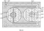
- FIG. 13 is a top view illustrating an LED chip according to another exemplary embodiment of the present disclosure.
- FIG. 14 is a top view illustrating an LED chip according to still another exemplary embodiment of the present disclosure.
- FIG. 15 is a top view illustrating an LED chip according to a further exemplary embodiment of the present disclosure.
- FIG. 16 is a top view illustrating an LED chip according to a further exemplary embodiment of the present disclosure.
- FIG. 17 is a top view illustrating an LED chip according to a further exemplary embodiment of the present disclosure.
- FIG. 18 is a top view illustrating an LED chip according to a further exemplary embodiment of the present disclosure.
- FIG. 19 is a cross-sectional diagram illustrating a display panel according to an exemplary embodiment of the present disclosure.
- the number of dead pixels in the Micro-LED display panel is multiplied, thereby affecting the yield of the display panel.
- a sapphire substrate 1 of the LED chip is removed, and a plurality of LED chips are bonded on a driving backboard, thereby achieving batch transfer of LED chips.
- a first contact electrode 6 or a second contact electrode 7 is connected to the driving backboard by a soldering process during the process of bonding, so that the circuit unit on the driving backboard can apply a voltage to the first contact electrode 6 and the second contact electrode 7 .
- the size of the first contact electrode 6 and the second contact electrode 7 is reduced to a few micrometers or even a few nanometers. Since the contact area is small, the bonding force of the first contact electrode 6 or the second contact electrode 7 with the driving backboard is reduced, and the probability of a soldering invalidation of the LED chip is increased, thereby causing an increase in the number of dead pixels in the Micro-LED display panel.
- the present disclosure provides a method of manufacturing an LED chip, by which a first extension electrode electrically connected to a first contact electrode is formed, a second extension electrode electrically connected to a second contact electrode is further formed, and both the first extension electrode and the second extension electrode include a plurality of concave spots for soldering.
- the concave spots for soldering can accommodate the solder, increasing the contact area of the solder with the first extension electrode and the second extension electrode. Therefore, the first extension electrode or the second extension electrode have a strong soldering force with the driving backboard, so that it is not easy to fall off from the driving backboard which leads to a phenomenon of soldering invalidation, thereby improving the yield of the display panel.
- FIG. 2 - FIG. 10 there are shown schematic diagrams illustrating respective steps of a method of manufacturing an LED chip according to an exemplary embodiment of the present disclosure. It should be noted that, in order to make the drawing concise and clear, one LED chip is taken as an example here.
- the method of manufacturing the LED chip includes the following processes.
- a substrate 100 is provided.
- the substrate 100 is used to provide a growth surface for a functional layer of an LED.
- the substrate 100 is a sapphire substrate and has a good lattice matching with a gallium nitride material.
- the substrate may also be silicon carbide.
- a first semiconductor layer 101 , an active layer 102 , and a second semiconductor layer 102 are sequentially formed on the substrate 100 .
- the first semiconductor layer 101 , the active layer 102 , and the second semiconductor layer 102 are used to form a core of a light emitting diode, as a functional layer of the LED chip.
- the first semiconductor layer 101 is made of N-type gallium nitride.
- the active layer 102 is a quantum well layer of an indium gallium nitride material.
- the second semiconductor layer 103 is made of P-type gallium nitride.
- the first semiconductor layer 101 , the active layer 102 , and the second semiconductor layer 102 may be formed by a process of metal organic chemical vapor deposition (MOCVD).
- MOCVD metal organic chemical vapor deposition
- a first contact electrode 106 extending through the active layer 102 and the second semiconductor layer 103 and electrically connected to the first semiconductor layer 101 is formed, and a second contact electrode 107 electrically connected to the second semiconductor layer 103 is formed on the second semiconductor layer 103 .
- the first contact electrode 106 and the second contact electrode 107 are used to apply a voltage to the first semiconductor layer 101 and the second semiconductor layer 103 , respectively.
- a first opening 104 extending through the active layer 102 and the second semiconductor layer 103 and exposing the first semiconductor layer 101 is formed.
- the first opening 104 is formed by patterning the active layer 102 and the second semiconductor layer 103 by a MESA photolithography.
- a groove extending through the first semiconductor layer 101 , the active layer 102 , and the second semiconductor layer 103 and exposing the substrate 100 is formed by an isolation structure photolithography, to define an area for a single LED chip and isolate the LED chip from other LED chips.
- an ohmic contact layer 105 is further formed on the second semiconductor layer 103 in this exemplary embodiment, to reduce a contact resistance between the second contact electrode 107 and the second semiconductor layer 103 subsequently formed.
- the ohmic contact layer 105 is made of indium tin oxide.
- an indium tin oxide layer may be formed by a physical vapor deposition or sputtering process, and then the indium tin oxide layer on the bottom and sidewall of the first opening 104 is removed by photolithography, to form the ohmic contact layer 105 located in a surface of the second semiconductor layer 103 .
- a first insulating layer 108 is formed for isolating the subsequently formed first contact electrode 106 and second contact electrode 107 .
- a first insulating material layer is formed on the bottom and sidewall of the first opening 104 , and on the second semiconductor layer 103 .
- the first insulating material layer is patterned to expose the bottom of the first opening (as shown in FIG. 4 ) and form a second opening (not shown) on the second semiconductor layer 103 , to form the first insulating layer 108 .
- the first insulating layer 108 defines positions of the first contact electrode 106 and the second contact electrode 107 at the first opening 104 and the second opening, respectively.
- the ohmic contact layer 105 is formed on the second semiconductor layer 103 , and the first insulating material layer is in contact with the ohmic contact layer 105 on the second semiconductor layer 103 when the first insulating material layer is formed.
- the second opening exposes the ohmic contact layer 105 above the second semiconductor layer 103 , when the second opening is formed.
- the first insulating layer 108 is made of silicon oxide or silicon nitride.
- the first insulating material layer may be patterned by a photolithography process to form a first insulating layer 108 .
- a first contact electrode 106 is formed in the first opening 104 (shown in FIG. 4 ), and a second contact electrode 107 is formed in the second opening (not shown).
- the first opening 104 and the second opening are filled with a second conductive layer, the second conductive layer and the first insulating material layer are planarized, and the second conductive layer located in the first opening 104 (as shown in FIG. 4 ) is used to constitute the first contact electrode 106 .
- the second conductive layer located in the second opening is used to constitute the second contact electrode 107 .
- the surfaces of the first contact electrode 106 and the second contact electrode 107 are flush with each other to constitute a forming surface A.
- the first insulating layer 108 is also flush with the surfaces of the first contact electrode 106 and the second contact electrode 107 , providing a basis for subsequent formation of the first extension electrode and the second extension electrode.
- a first extension electrode 111 electrically connected to the first contact electrode 106 is formed on the first contact electrode 106 , and the first extension electrode 111 includes a plurality of concave spots 130 for soldering.
- a second extension electrode 121 electrically connected to the second contact electrode 107 and isolated from the first extension electrode 111 is formed on the second contact electrode 107 , and the second extension electrode 121 includes a plurality of concave spots 130 for soldering.
- the first extension electrode 111 is an extension electrode of the first contact electrode 106 , and a plurality of concave spots 130 are formed in the first extension electrode 111 for placing solder and being soldered to the driving circuit, thereby implementing the electrical connection between the first contact electrode 106 and the driving circuit.
- the forming surface A is covered with nanoimprint lithography resist 140 .
- the nanoimprint lithography resist 140 may be a polymer film, and the forming surface A may be covered by the nanoimprint lithography resist 140 by a coating method.
- the nanoimprint lithography resist 140 has a thickness in a range of 1 ⁇ m to 10 ⁇ m.
- the nanoimprint lithography resist 140 (shown in FIG. 6 ) is patterned by nanoimprint lithography to form a nanoimprint pattern layer 109 .
- the nanoimprint pattern layer 109 serves as a mask for the subsequently formed first extension electrode and second extension electrode for defining the positions and patterns of the first extension electrode and the second extension electrode.
- a nanoimprint mould is provided, and the nanoimprint lithography resist 140 is imprinted by the mould, so that the pattern of the mould is transferred into the nanoimprint lithography resist 140 , thereby patterning the nanoimprint lithography resist 140 to form a nanoimprint pattern layer 109 .
- the first extension electrode and the second extension electrode are formed by two pattern transfers, and correspondingly, the pattern of the mould is consistent with the patterns of the first extension electrode and the second extension electrode to be formed.
- the position and pattern of the concave portion (or convex portion) pattern in the mould coincide with the position and pattern in which the concave portion (or convex portion) is formed in the first extension electrode and the second extension electrode.
- a first conductive layer 110 is formed on the forming surface A between the nanoimprint pattern layer 109 and the nanoimprint pattern layer 109 .
- the portion of the first conductive layer 110 located on the surface A is used to form the first extension electrode and the second extension electrode.
- the first conductive layer 110 is made of metal, such as gold, silver or aluminum.
- the metal may be reflective, thereby improving the light extraction efficiency of the LED chip.
- the first conductive layer 110 may be formed by an evaporation method. In other exemplary embodiments, the first conductive layer 110 may also be formed by a sputtering or electroplating process.
- the thickness of the first conductive layer 110 is smaller than the thickness of the nanoimprint pattern layer 109 , so that a top surface of the first conductive layer 110 on the forming surface A is lower than a top surface of the nanoimprint layer 109 such that the first conductive layer 110 on the forming surface A is isolated from the first conductive layer 110 on the top surface of the nanoimprint pattern layer 109 to facilitate to remove the first conductive layer 110 on the top surface of the nanoimprint pattern layer 109 by removal of the nanoimprint pattern in a subsequent process, and retain the first conductive layer 110 on the forming surface A.
- the thickness of the first conductive layer 110 is in a range of 20 nm to 2 ⁇ m.
- the first conductive layer 110 on the nanoimprint pattern layer 109 (shown in FIG. 8 ) is removed, and the first conductive layer 110 on the forming surface A is retained to constitute the first extension electrode 111 and the second extension electrode 121 .
- the nanoimprint pattern layer 109 After the nanoimprint pattern layer 109 is removed, a portion of the space occupied by the nanoimprint pattern layer 109 is used to form the concave spots 130 .
- the first conductive layer 110 on the nanoimprint pattern layer 109 is removed by a lift off process.
- the first conductive layer 110 on the nanoimprint pattern layer 109 may be lifted off by a tape.
- the nanoimprint pattern layer 109 is removed.
- the nanoimprint pattern layer 109 is removed by an etching process.
- the etching process may be a dry or wet etching process.
- each of the first extension electrode 111 and the second extension electrode 121 is a circular extension electrode, and an entire area of the circular extension electrode is used to form a plurality of concave spots 130 .
- the solder is likely to form a circular extension surface.
- a circular extension electrode with a plurality of concave spots 130 is formed, which matches the shape of the circular extension surface. A larger soldering area can be obtained by a smaller extension electrode area, thereby improving the utilization ratio of the first extension electrode 111 and the second extension electrode 121 .
- each of the plurality of concave spots 130 shown in FIG. 10 has a circular shape.
- the process of the circular concave spot 130 is relatively simple, and the manufacturing efficiency of the LED chip is improved.
- first extension electrode and the second extension electrode of other shapes may also be formed, and the plurality of concave spots may be formed on all or a part of the first extension electrode and the second extension electrode.
- the concave spot may also be in the shape of a triangle, a square, or the like.
- the first extension electrode and the second extension electrode are formed by providing different moulds.
- first extension electrode and the second extension electrode are formed by a nanoimprint lithography process.
- first extension electrode and the second extension electrode may also be formed by a photolithography process.
- the second insulating layer 112 may be formed between the first extension electrode 111 and the second extension electrode 121 .
- the second insulating layer 112 is used to achieve isolation between the first extension electrode 111 and the second extension electrode 121 .
- a second insulating material layer is formed on the first extension electrode 111 and the second extension electrode 121 , and the forming surface A between the first extension electrode 111 and the second extension electrode 121 , and the second insulation material layer is patterned to form the second insulating layer 112 .
- the second insulating layer 112 is made of silicon nitride, silicon oxide or the like.
- the second insulating material layer may be patterned by a photolithography process to form the second insulating layer 112 .
- the thickness of the second insulating layer 112 is greater than the thickness of the first extension electrode 111 or the second extension electrode 121 .
- the second insulating layer 112 can also physically isolate the solder on the different extension electrodes during the soldering process, thereby achieving electrical isolation.
- the thickness of the second insulating layer 112 is in a range of 1 ⁇ m to 10 ⁇ m.
- the second insulating layer may not be formed, and when the LED chip is soldered to the driving circuit, precise soldering process control can prevent solders respectively located on the first extension electrode and the second extension electrode from being connected together, thereby avoiding a short circuit between the first extension electrode and the second extension electrode.
- the driving backboard includes a plurality of circuit units, and the first extension electrode 111 of the LED chip is connected to the first electrical terminal of the circuit unit, and the second extension electrode 121 of the LED chip is connected to the second electrical terminal.
- a voltage is applied to the first contact electrode 106 and the second contact electrode 107 of the LED chip through the circuit unit, thereby causing the active layer 102 in the LED chip to emit light.
- the first extension electrode 111 is soldered to the first electrical terminal of the driving backboard
- the second extension electrode 121 is soldered to the second electrical terminal of the driving backboard.
- the concave spots 130 in the first extension electrode 111 and the second extension electrode 121 are used for soldering, and the solder located in the concave spots 130 can increase the area of contact between the solder with the first extension electrode 111 and the second extension electrode 121 , thereby improving the soldering strength and preventing the LED chip from falling off the driving backboard, in turn, reducing the probability of the generation of dead pixels, and increasing the yield.
- the present disclosure further provides an LED chip including a first extension electrode electrically connected to the first contact electrode, and a second extension electrode electrically connected to the second contact electrode.
- Each of the first extension electrode and the second extension electrode includes a plurality of concave spots for soldering.
- the concave spots for soldering can accommodate the solder, increasing the area of contact of the solder with the first extension electrode and the second extension electrode.
- the first extension electrode or second extension electrode may have strong soldering force with the driving backboard, so that it is not easy to fall off from the driving backboard which leads to a phenomenon of solder invalidation, thereby improving the yield of the display panel.
- the LED chip includes:
- first semiconductor layer 101 a first semiconductor layer 101 , an active layer 102 and a second semiconductor layer 103 sequentially located on the first semiconductor layer 101 .
- the first semiconductor layer 101 , the active layer 102 , and the second semiconductor layer 102 are used to constitute a core of a light emitting diode, which is a functional layer of the LED chip.
- the first semiconductor layer 101 is located on the substrate 100 .
- the first semiconductor layer 101 is made of N-type gallium nitride.
- the active layer 102 is a quantum well layer of an indium gallium nitride material.
- the second semiconductor layer 103 is made of P-type nitride. gallium.
- a first contact electrode 106 extends through the active layer 102 and the second semiconductor layer 103 and is electrically connected to the first semiconductor layer 101 .
- a second contact electrode 107 is located on the second semiconductor layer 103 and is electrically connected to the second semiconductor layer 103 .
- the first contact electrode 106 and the second contact electrode 107 are respectively used to apply a voltage to the first semiconductor layer 101 and the second semiconductor layer 103 .
- the surfaces of the first contact electrode 106 and the second contact electrode 107 are flush with each other to constitute the forming surface A.
- a first insulating layer 108 is further formed between the first contact electrode 106 and the active layer 102 and the second semiconductor layer 103 for electrically isolating the first contact electrode 106 from the active layer 102 and the second semiconductor layer 103 .
- first insulating layer 108 is also located above the second semiconductor layer 103 and between the first contact electrode 106 and the second contact electrode 107 .
- the first insulating layer 108 is flush with the surfaces of the first contact electrode 106 and the second contact electrode 107 .
- the first insulating layer 108 is made of silicon oxide or silicon nitride.
- An ohmic contact layer 105 is further formed between the second semiconductor layer 103 and the second contact electrode 107 for reducing the contact resistance between the second contact electrode 107 and the second semiconductor layer 103 .
- the ohmic contact layer 105 is made of indium tin oxide.
- the LED chip further includes: a first extension electrode 111 located on the first contact electrode 106 and electrically connected to the first contact electrode 106 , and including a plurality of concave spots for soldering; and a second extension electrode 121 located on the second contact electrode 107 , electrically connected to the second contact electrode 107 , isolated from the first extension electrode 111 , and including a plurality of concave spots 130 for soldering.
- each of the first extension electrode 111 and the second extension electrode 121 is a circular extension electrode, and an entire area of the circular extension electrode is used to form the plurality of concave spots 130 .
- the solder is likely to form a circular extension surface.
- the circular extension electrode with a plurality of concave points 130 in the LED chip of the exemplary embodiment matches the shape of the circular extension surface. A larger soldering area can be obtained by a smaller extension electrode area, thereby improving the utilization ratio of the first extension electrode 111 and the second extension electrode 121 .
- each of the first extension electrode and the second extension electrode may further have other shapes, for example, may be an elliptical extension electrode, a racetrack-shaped extension electrode, a polygonal extension electrode, etc., and the plurality of concave spots are formed in the entire area of the extension electrode.
- the first contact electrode 106 and the second contact electrode 107 are circular contact electrodes.
- a projected area of the circular extension electrode on the forming surface A is larger than a projected area of the circular contact electrode on the forming surface A. That is, the projected areas of the first extension electrode 111 and the second extension electrode 121 on the forming surface A are large, so that the soldering areas of the first extension electrode 111 and the second extension electrode 121 can be increased.
- the first contact electrode 106 extends through the active layer 102 and the second semiconductor layer 103 .
- the first contact electrode 106 is generally an electrode having a small cross section, which can reduce the influence of the first contact electrode 106 on the LED illumination area.
- the increase in the area of the first extension electrode 111 does not affect the LED illumination area. Therefore, by increasing the area of the first extension electrode 111 , the soldering area of the first extension electrode 111 and the driving circuit can be increased, thereby improving the soldering strength of the first contact electrode 106 and the driving circuit.
- the projected areas of the first extension electrode and the second extension electrode may be equal to or slightly smaller than the projected areas of the first contact electrode and the second contact electrode. Because a plurality of concave spots are formed in the first extension electrode and the second extension electrode, the sidewalls of the plurality of concave spots can still function to increase the soldering area, thereby increasing the soldering strength.
- the projection of the circular extension electrode and the circular contact electrode on the forming surface A constitutes a structure of concentric circles.
- the solder is located at the center of the concentric circles, which ensures a large area of contact between the driving circuit and the circular extension electrode, and between the circular extension electrode and the circular contact electrode, thereby increasing the soldering strength.
- the first extension electrode is electrically connected to the first contact electrode
- the second extension electrode is electrically connected to the second contact electrode.
- the projection of the circular extension electrode and the circular contact electrode on the forming surface A may also be in a structure with intersecting circles, inscribed circles or an inner circular.
- the first extension electrode 111 and the second extension electrode 121 are made of metal, such as gold, silver or aluminum.
- the metal can be reflective, thereby improving the light extraction efficiency of the LED chip.
- the first extension electrode and the second extension electrode may also be made of other conductive materials.
- the thickness of each of the first extension electrode 111 and the second extension electrode 121 is in a range of 20 nm to 2 ⁇ m.
- the concave spots 130 located in the first extension electrode 111 and the second extension electrode 121 are circular, and the process of forming the circular concave spots is relatively simple.
- the size of the opening of the concave spot 130 is too large (or the spacing between adjacent concave spots 130 is too small), it is easy to affect the contact area between the first extension electrode 111 and the first contact electrode 106 or between the second extension electrode 121 and the second contact electrode 107 , thereby affecting the electrical connection effect. If the opening size of the concave spots 130 is too small (or the spacing between adjacent concave spots 130 is too large), it is not conducive to the increase in the soldering area, and further influencing the soldering effect.
- the opening size of the concave spot 130 is in a range of 8 nm to 10 ⁇ m
- the spacing between adjacent concave spots in the first extension electrode 111 or the second extension electrode 121 is in a range of 8 nm to 10 ⁇ m.
- the LED chip further includes: a second insulating layer 112 between the first extension electrode 111 and the second extension electrode 121 , for isolating the first extension electrode 111 from the second extension electrode 121 .
- the thickness of the second insulating layer 112 is greater than the thickness of the first extension electrode 111 or the second extension electrode 121 .
- the second insulating layer 112 can physically isolate the solder on the different extension electrodes during the soldering process, thereby achieving electrical isolation.
- the thickness of the second insulating layer 112 is in a range of 1 ⁇ m to 10 ⁇ m.
- the second insulating layer 112 is made of silicon nitride, silicon oxide or the like.
- the second insulating layer may not be disposed, and when the LED chip is soldered to the driving circuit, the solders respectively located on the first extension electrode and the second extension electrode are not connected together by precise soldering process control, thereby avoiding a short circuit between the first extension electrode and the second extension electrode.
- FIG. 13 a top view of an LED chip according to another exemplary embodiment of the present disclosure is shown.
- the same points in this exemplary embodiment as the previous exemplary embodiment will not be described again.
- the difference is that a partial area of the first extension electrode in the LED chip of this exemplary embodiment is used to form a plurality of concave spots.
- the first contact electrode 406 includes a primary contact electrode 4061 , and two auxiliary contact electrodes 4062 that are isolated from the primary contact electrode 4061 .
- the primary contact electrode 4061 is an electrode having a large contact area and corresponding to the soldering position.
- the primary contact electrode 4061 and the auxiliary contact electrode 4062 are isolated from each other and distributed at different positions of the LED chip, which can increase the current distribution in the LED chip and enhance the uniformity of the light emitted from the LED chip.
- the number of the auxiliary contact electrodes 4062 is two. In other exemplary embodiments, the number of the auxiliary contact electrodes 4062 is at least one in order to increase the current distribution.
- the first extension electrode 411 includes a primary extension electrode 4111 covering the primary contact electrode 4061 , a secondary extension electrode 4112 covering the auxiliary contact electrode 4062 , and a linear extension electrode 4113 connecting the primary extension electrode 4111 and the auxiliary extension electrode 4112 .
- a circular area (shown by a broken line) of the primary extension electrode 4111 above the primary contact electrode 4061 is formed with a plurality of concave spots 430 for achieving soldering.
- the solder In the subsequent soldering process, the solder easily is likely to form a circular extension surface, and a circular area in which a plurality of concave spots 430 are formed in the first extension electrode 411 matches the shape of the circular extension surface.
- the surfaces of the first contact electrode 406 and the second contact electrode 407 are flush with each other to constitute a forming surface (not shown).
- the primary contact electrode 4061 is a circular contact electrode, and a projected area of the circular area on the forming surface is larger than a projected area of the circular contact electrode on the forming surface. That is, the circular area for soldering has a large projected area, which can increase the soldering area between the LED chip and the driving circuit, thereby increasing the soldering strength.
- the circular area may also be equal to or slightly smaller than the projected area of the circular contact electrode.
- the projection of the circular area on the forming surface and the projection of the circular contact electrode on the forming surface constitute a structure with concentric circles.
- the solder is located at the center of the concentric circles. It can be ensured that there is a large area of contact between the driving circuit and the circular area of the first extension electrode 411 , and between the circular area of the first extension electrode 411 and the circular contact electrode, thereby improving the welding strength.
- the projection of the circular region and the circular contact electrode on the forming surface may also be in a structure with intersecting circles, inscribed circles or an inner circular.
- the second contact electrode 407 includes a circular primary contact electrode, and two linear extension electrodes connected to the circular primary contact electrode, which can increase the current distribution in the LED chip and enhance the uniformity of the light emitted from the LED chip.
- the second extension electrode 412 is a circular extension electrode covering the circular primary contact electrode, and the entire area of the circular extension electrode is used to form a plurality of concave spots 430 . That is, in this exemplary embodiment, the second extension electrode 412 does not completely cover the second contact electrode 407 .
- FIG. 14 a schematic diagram illustrating an LED chip according to still another exemplary embodiment of the present disclosure is shown.
- the same points of the LED chip in this exemplary embodiment as the exemplary embodiments shown in FIG. 11 and FIG. 12 are not described again.
- the difference is that a partial area of the second extension electrode 521 in the LED chip of this exemplary embodiment is used to form the plurality of concave spots 530 .
- the second contact electrode 507 includes a primary contact electrode 5071 and two extension electrodes 5072 connected to the primary contact electrode 5071 , to increase the current distribution in the LED chip, thereby enhancing the uniformity of the light emitted from the LED chip.
- the number of the extension electrodes 5072 is two. In other exemplary embodiments, the number of the extension electrodes 5072 is at least one in order to increase the current distribution.
- the second extension electrode 521 covers the primary contact electrode 5071 and the elongated electrode 5072 , and there is a large area of contact between the second extension electrode 521 and the second contact electrode 507 , thereby improving the reliability of the electrical connection between the second extension electrode 521 and the second contact electrode 507 .
- the circular area (an area around by a dashed line) of the second extension electrode 521 located above the primary contact electrode 5071 is formed with a plurality of concave spots 530 for soldering.
- the solder is likely to form a circular extension surface, and the circular area formed with the concave spots 530 in the second extension electrode 521 matches the shape of the circular extension surface.
- the primary contact electrode 5071 is a circular contact electrode, and a projected area of the circular area on the forming surface is larger than a projected area of the circular contact electrode on the forming surface. That is, the circular area for soldering has a large projected area, which can increase the soldering area between the LED chip and the driving circuit, thereby increasing the soldering strength.
- the projection of the circular area and the circular contact electrode on the forming surface constitutes a structure with concentric circles.
- the solder is located at the center of the concentric circles. It can be ensured that there is a large area of contact between the driving circuit and the circular area of the second extension electrode 521 , and between the circular area of the second extension electrode 521 and the circular contact electrode, thereby increasing the soldering strength.
- the projection of the circular region and the circular contact electrode on the forming surface may also be in a structure with intersecting circles, inscribed circles or an inner circular.
- the first contact electrode 506 is a circular primary contact electrode
- the first extension electrode 511 covers the circular primary contact electrode
- a partial area (circular area) of the first extension electrode 511 is used to form the plurality of concave spots 530 .
- the first extension electrode 511 is electrically insulated from the first extension electrode 521 by the second insulation layer 512 .
- a partial area (circular area) of each of the first extension electrode 511 and the second extension electrode 521 is formed with the concave spots 530 for soldering in.
- an entire area of each of the first extension electrode 611 and the second extension electrode 621 may be formed with concave spots 630 for soldering.
- any region of the solder located at the first extension electrode 611 or the second extension electrode 621 may be formed in the concave spot 630 , which reduces the difficulty in alignment of soldering positions, thereby enhancing the soldering strength.
- the first contact electrode or the second contact electrode is a circular contact electrode, or the primary contact electrode of the first contact electrode or the second contact electrode is a circular contact electrode.
- the first extension electrode or the second extended electrode is used for realizing the soldering contact. Therefore, the shape of the first contact electrode or the second contact electrode may be other shapes.
- the first contact electrode 706 or the second contact electrode 707 may be a strip electrode.
- the first contact electrode or the second contact electrode may also be a square electrode, an elliptical electrode, a trapezoidal electrode or the like.
- the shapes of the concave spots in the first extension electrode or the second extension electrode are all circular.
- the concave spots in the LED chip according to the present disclosure may be in other shapes.
- the concave spots 206 are square in shape; or, as shown in FIG. 18 , the concave spots 306 are triangular in shape.
- the shape of the concave spot may also be a regular pentagon, a regular hexagon, or other regular polygons.
- the concave spots can also be irregular shaped concave spots.
- the LED chip provided by the present disclosure may be formed by the method of manufacturing the LED chip provided by the present disclosure, or may be formed by other manufacturing methods.
- the present disclosure also provides a display panel, and with reference to FIG. 19 , a schematic view illustrating a display panel according to an exemplary embodiment of the present disclosure is shown.
- the display panel includes:
- a driving backboard 20 includes a substrate 24 , and a plurality of circuit units (not shown) located on the substrate 24 , the circuit units each including a first electrical terminal 21 and a second electrical terminal 22 used to apply a voltage to LED chip; and
- the LED chip is an LED chip provided by the present disclosure, and the related description is not repeated herein.
- the first extension electrode 111 is electrically connected to the first contact electrode 106
- the first contact electrode 106 is electrically connected to the first semiconductor layer 101 . Therefore, the circuit unit applies a voltage to the first semiconductor layer 101 by the first electrical terminal 21 .
- the second extension electrode 121 is electrically connected to the second contact electrode 107
- the second contact electrode 107 is electrically connected to the second semiconductor layer 103 . Therefore, the circuit applies a voltage to the second semiconductor layer 103 by the second electrical terminal 22 . After the voltage is applied to the first semiconductor layer 101 and the second semiconductor layer 103 , the active layer 102 emits light, and light is emitted from a side close to the first semiconductor layer 101 .
- the first semiconductor layer 101 is an N-type semiconductor layer
- the second semiconductor layer 102 is a P-type semiconductor layer.
- the first electrical terminal 21 is a negative connection terminal
- the second electrical terminal 22 is a positive connection terminal.
- the substrate 24 may be a rigid substrate, or may be a flexible substrate, a folded substrate, or a stretched substrate.
- the present disclosure also provides an electronic device including the display panel provided by the present disclosure.
- the probability of occurrence of a dead pixel in the display panel is small, and accordingly, the electronic device has good reliability, long service life, and low repair rate.
- the electronic device may be a mobile phone, a near-eye display device (VR or AR), a television, a wearable device, or the like.
- VR near-eye display device
- AR television
- wearable device or the like.
Abstract
Description
Claims (20)
Applications Claiming Priority (4)
| Application Number | Priority Date | Filing Date | Title |
|---|---|---|---|
| CN201810187158.2 | 2018-03-07 | ||
| CN201810187158.2A CN110246945B (en) | 2018-03-07 | 2018-03-07 | LED chip, manufacturing method thereof, display panel and electronic equipment |
| CN201810187158 | 2018-03-07 | ||
| PCT/CN2018/089793 WO2019169770A1 (en) | 2018-03-07 | 2018-06-04 | Led chip and manufacturing method therefor, display panel and electronic device |
Related Parent Applications (1)
| Application Number | Title | Priority Date | Filing Date |
|---|---|---|---|
| PCT/CN2018/089793 Continuation WO2019169770A1 (en) | 2018-03-07 | 2018-06-04 | Led chip and manufacturing method therefor, display panel and electronic device |
Publications (2)
| Publication Number | Publication Date |
|---|---|
| US20190273184A1 US20190273184A1 (en) | 2019-09-05 |
| US10868217B2 true US10868217B2 (en) | 2020-12-15 |
Family
ID=67768739
Family Applications (1)
| Application Number | Title | Priority Date | Filing Date |
|---|---|---|---|
| US16/416,298 Active US10868217B2 (en) | 2018-03-07 | 2019-05-20 | LED chips, method of manufacturing the same, and display panels |
Country Status (1)
| Country | Link |
|---|---|
| US (1) | US10868217B2 (en) |
Families Citing this family (3)
| Publication number | Priority date | Publication date | Assignee | Title |
|---|---|---|---|---|
| DE102019101544A1 (en) * | 2018-01-24 | 2019-07-25 | Osram Opto Semiconductors Gmbh | Optoelectronic component and method |
| CN112909153B (en) * | 2019-12-03 | 2022-12-16 | 深圳市聚飞光电股份有限公司 | Flip LED chip, circuit board and electronic equipment |
| CN114755852B (en) * | 2022-04-21 | 2024-03-29 | 南京京东方显示技术有限公司 | Backboard, backboard processing method, backlight module and display device |
Citations (16)
| Publication number | Priority date | Publication date | Assignee | Title |
|---|---|---|---|---|
| US7456438B2 (en) * | 2005-10-17 | 2008-11-25 | Samsung Electro-Mechanics Co., Ltd. | Nitride-based semiconductor light emitting diode |
| EP2388836A2 (en) | 2010-05-18 | 2011-11-23 | Seoul Opto-Devices Co., Ltd. | High-efficiency light-emitting diode and method of fabricating the same |
| CN103247743A (en) | 2013-05-24 | 2013-08-14 | 安徽三安光电有限公司 | Veneering type lighting device and manufacturing method thereof |
| JP2013201156A (en) | 2012-03-23 | 2013-10-03 | Toshiba Corp | Semiconductor light-emitting element and method of manufacturing the same |
| US20130264603A1 (en) | 2012-04-09 | 2013-10-10 | Advanced Optoelectronic Technology, Inc. | Surface-mounting led chip |
| US8557616B2 (en) * | 2009-12-09 | 2013-10-15 | Nano And Advanced Materials Institute Limited | Method for manufacturing a monolithic LED micro-display on an active matrix panel using flip-chip technology and display apparatus having the monolithic LED micro-display |
| US20140034981A1 (en) * | 2012-08-01 | 2014-02-06 | Epistar Corporation | Light emitting diode structure |
| US8653551B2 (en) * | 2011-01-14 | 2014-02-18 | Rohm Co., Ltd. | Light-emitting element |
| CN104091874A (en) | 2014-07-01 | 2014-10-08 | 天津三安光电有限公司 | Light emitting diode |
| WO2014192226A1 (en) | 2013-05-31 | 2014-12-04 | 信越半導体株式会社 | Light-emitting element |
| CN105702823A (en) | 2016-04-11 | 2016-06-22 | 聚灿光电科技股份有限公司 | Small-sized light emitting diode (LED) chip and fabrication method thereof |
| CN105870346A (en) | 2016-04-15 | 2016-08-17 | 深圳市华星光电技术有限公司 | Manufacturing method of LED display screen and LED display screen |
| US20170110629A1 (en) * | 2014-07-01 | 2017-04-20 | Seoul Viosys Co., Ltd. | Light emitting element |
| CN107340656A (en) | 2017-09-08 | 2017-11-10 | 深圳市华星光电技术有限公司 | Pixel electrode and preparation method, display panel |
| CN107546303A (en) | 2017-08-25 | 2018-01-05 | 扬州乾照光电有限公司 | A kind of AlGaInP based light-emitting diodes and its manufacture method |
| TW201807840A (en) | 2016-08-18 | 2018-03-01 | 新世紀光電股份有限公司 | Micro light emitting diode and manufacturing method thereof |
-
2019
- 2019-05-20 US US16/416,298 patent/US10868217B2/en active Active
Patent Citations (22)
| Publication number | Priority date | Publication date | Assignee | Title |
|---|---|---|---|---|
| US7456438B2 (en) * | 2005-10-17 | 2008-11-25 | Samsung Electro-Mechanics Co., Ltd. | Nitride-based semiconductor light emitting diode |
| US8557616B2 (en) * | 2009-12-09 | 2013-10-15 | Nano And Advanced Materials Institute Limited | Method for manufacturing a monolithic LED micro-display on an active matrix panel using flip-chip technology and display apparatus having the monolithic LED micro-display |
| EP2388836A2 (en) | 2010-05-18 | 2011-11-23 | Seoul Opto-Devices Co., Ltd. | High-efficiency light-emitting diode and method of fabricating the same |
| US8653551B2 (en) * | 2011-01-14 | 2014-02-18 | Rohm Co., Ltd. | Light-emitting element |
| JP2013201156A (en) | 2012-03-23 | 2013-10-03 | Toshiba Corp | Semiconductor light-emitting element and method of manufacturing the same |
| US20130264603A1 (en) | 2012-04-09 | 2013-10-10 | Advanced Optoelectronic Technology, Inc. | Surface-mounting led chip |
| CN103367591A (en) | 2012-04-09 | 2013-10-23 | 展晶科技(深圳)有限公司 | Light-emitting diode chip |
| US20140034981A1 (en) * | 2012-08-01 | 2014-02-06 | Epistar Corporation | Light emitting diode structure |
| CN103247743A (en) | 2013-05-24 | 2013-08-14 | 安徽三安光电有限公司 | Veneering type lighting device and manufacturing method thereof |
| US10559732B2 (en) | 2013-05-24 | 2020-02-11 | Xiamen Sanan Opto Electronics Technology Co., Ltd. | Surface-mounted light-emitting device and fabrication method thereof |
| WO2014192226A1 (en) | 2013-05-31 | 2014-12-04 | 信越半導体株式会社 | Light-emitting element |
| TW201505211A (en) | 2013-05-31 | 2015-02-01 | Shinetsu Handotai Kk | Light-emitting element |
| US20170110629A1 (en) * | 2014-07-01 | 2017-04-20 | Seoul Viosys Co., Ltd. | Light emitting element |
| US10038120B2 (en) | 2014-07-01 | 2018-07-31 | Xiamen Sanan Optoelectronics Technology Co., Ltd. | Light emitting diode |
| CN104091874A (en) | 2014-07-01 | 2014-10-08 | 天津三安光电有限公司 | Light emitting diode |
| CN105702823A (en) | 2016-04-11 | 2016-06-22 | 聚灿光电科技股份有限公司 | Small-sized light emitting diode (LED) chip and fabrication method thereof |
| CN105870346A (en) | 2016-04-15 | 2016-08-17 | 深圳市华星光电技术有限公司 | Manufacturing method of LED display screen and LED display screen |
| US20180108871A1 (en) | 2016-04-15 | 2018-04-19 | Shenzhen China Star Optoelectronics Technology Co., Ltd. | Manufacturing method for led display panel and led display panel |
| TW201807840A (en) | 2016-08-18 | 2018-03-01 | 新世紀光電股份有限公司 | Micro light emitting diode and manufacturing method thereof |
| US20180090639A1 (en) | 2016-08-18 | 2018-03-29 | Genesis Photonics Inc. | Micro light emitting diode and manufacturing method thereof |
| CN107546303A (en) | 2017-08-25 | 2018-01-05 | 扬州乾照光电有限公司 | A kind of AlGaInP based light-emitting diodes and its manufacture method |
| CN107340656A (en) | 2017-09-08 | 2017-11-10 | 深圳市华星光电技术有限公司 | Pixel electrode and preparation method, display panel |
Non-Patent Citations (2)
| Title |
|---|
| CN First Office Action with search report dated Jan. 6, 2020 in the corresponding CN application(application No. 201810187158.2). |
| TW Office Action dated Sep. 28, 2018 in the corresponding TW application (application No. 107209071). |
Also Published As
| Publication number | Publication date |
|---|---|
| US20190273184A1 (en) | 2019-09-05 |
Similar Documents
| Publication | Publication Date | Title |
|---|---|---|
| US9825013B2 (en) | Transfer-bonding method for the light emitting device and light emitting device array | |
| US10964722B2 (en) | Micro LED display substrate, method for manufacturing the same, and display device | |
| US10643981B2 (en) | Emissive display substrate for surface mount micro-LED fluidic assembly | |
| WO2021017497A1 (en) | Display panel, display device and manufacturing method for display panel | |
| US10797124B2 (en) | Organic light emitting display substrate and manufacturing method thereof | |
| US10868217B2 (en) | LED chips, method of manufacturing the same, and display panels | |
| US11081680B2 (en) | Pixel structure, method for forming the same, and display screen | |
| US20210336074A1 (en) | Method of fabricating a micro light emitting diode display substrate, and micro light emitting diode display substrate | |
| TWI521690B (en) | Transfer-bonding method for light-emitting devices and light-emitting device array | |
| WO2021115472A1 (en) | Micro-led chip and manufacturing method therefor | |
| WO2019169770A1 (en) | Led chip and manufacturing method therefor, display panel and electronic device | |
| JP7460650B2 (en) | Light-emitting element for display and display device having same | |
| WO2020238395A1 (en) | Led chip and method for fabrication thereof, chip wafer, and micro-led display device | |
| KR102614588B1 (en) | Method of manufacturing display apparatus | |
| US11876156B2 (en) | Light emitting device | |
| JP2022070551A (en) | Light source device, display device, and manufacturing method for light source device | |
| WO2020087806A1 (en) | Epitaxial substrate and manufacturing method therefor | |
| KR101026216B1 (en) | Light emitting diode and method for fabricating the same | |
| CN116565103B (en) | Micro LED micro display chip and manufacturing method thereof | |
| US11227975B2 (en) | Semiconductor structure having a bridge layer | |
| US11961873B2 (en) | Light emitting device for display and display apparatus having the same | |
| CN211088273U (en) | Light emitting element for display and display device having the same | |
| US20210351229A1 (en) | Light emitting device for display and display apparatus having the same | |
| CN211654819U (en) | Light emitting element for display and display device having the same | |
| CN112909136A (en) | Light emitting diode, display panel, display device and preparation method |
Legal Events
| Date | Code | Title | Description |
|---|---|---|---|
| FEPP | Fee payment procedure |
Free format text: ENTITY STATUS SET TO UNDISCOUNTED (ORIGINAL EVENT CODE: BIG.); ENTITY STATUS OF PATENT OWNER: LARGE ENTITY |
|
| STPP | Information on status: patent application and granting procedure in general |
Free format text: DOCKETED NEW CASE - READY FOR EXAMINATION |
|
| STPP | Information on status: patent application and granting procedure in general |
Free format text: NON FINAL ACTION MAILED |
|
| AS | Assignment |
Owner name: KUNSHAN GO-VISIONOX OPTO-ELECTRONICS CO., LTD., CHINA Free format text: ASSIGNMENT OF ASSIGNORS INTEREST;ASSIGNORS:WEI, DONG;XING, RUBO;LIU, HUIMIN;AND OTHERS;REEL/FRAME:054116/0423 Effective date: 20190505 Owner name: KUNSHAN NEW FLAT PANEL DISPLAY TECHNOLOGY CENTER CO., LTD., CHINA Free format text: ASSIGNMENT OF ASSIGNORS INTEREST;ASSIGNORS:WEI, DONG;XING, RUBO;LIU, HUIMIN;AND OTHERS;REEL/FRAME:054116/0423 Effective date: 20190505 |
|
| STPP | Information on status: patent application and granting procedure in general |
Free format text: PUBLICATIONS -- ISSUE FEE PAYMENT RECEIVED |
|
| STCF | Information on status: patent grant |
Free format text: PATENTED CASE |
|
| AS | Assignment |
Owner name: CHENGDU VISTAR OPTOELECTRONICS CO., LTD., CHINA Free format text: ASSIGNMENT OF ASSIGNORS INTEREST;ASSIGNORS:KUNSHAN NEW FLAT PANEL DISPLAY TECHNOLOGY CENTER CO., LTD.;KUNSHAN GO-VISIONOX OPTO-ELECTRONICS CO., LTD.;REEL/FRAME:054527/0066 Effective date: 20201125 |