US10763301B2 - Display device - Google Patents
Display device Download PDFInfo
- Publication number
- US10763301B2 US10763301B2 US16/159,025 US201816159025A US10763301B2 US 10763301 B2 US10763301 B2 US 10763301B2 US 201816159025 A US201816159025 A US 201816159025A US 10763301 B2 US10763301 B2 US 10763301B2
- Authority
- US
- United States
- Prior art keywords
- region
- pad
- electrode layer
- mesh shape
- length
- Prior art date
- Legal status (The legal status is an assumption and is not a legal conclusion. Google has not performed a legal analysis and makes no representation as to the accuracy of the status listed.)
- Active
Links
- 239000000758 substrate Substances 0.000 claims abstract description 13
- 239000002184 metal Substances 0.000 claims description 15
- 229910052751 metal Inorganic materials 0.000 claims description 15
- QPLDLSVMHZLSFG-UHFFFAOYSA-N Copper oxide Chemical compound [Cu]=O QPLDLSVMHZLSFG-UHFFFAOYSA-N 0.000 claims description 5
- 239000005751 Copper oxide Substances 0.000 claims description 5
- 229910000431 copper oxide Inorganic materials 0.000 claims description 5
- 239000010410 layer Substances 0.000 description 145
- 230000000712 assembly Effects 0.000 description 33
- 238000000429 assembly Methods 0.000 description 33
- CEOCDNVZRAIOQZ-UHFFFAOYSA-N pentachlorobenzene Chemical compound ClC1=CC(Cl)=C(Cl)C(Cl)=C1Cl CEOCDNVZRAIOQZ-UHFFFAOYSA-N 0.000 description 24
- RYGMFSIKBFXOCR-UHFFFAOYSA-N Copper Chemical compound [Cu] RYGMFSIKBFXOCR-UHFFFAOYSA-N 0.000 description 16
- 229910052802 copper Inorganic materials 0.000 description 16
- 239000010949 copper Substances 0.000 description 16
- 239000011347 resin Substances 0.000 description 14
- 229920005989 resin Polymers 0.000 description 14
- 239000012790 adhesive layer Substances 0.000 description 12
- 238000002834 transmittance Methods 0.000 description 12
- BQCADISMDOOEFD-UHFFFAOYSA-N Silver Chemical compound [Ag] BQCADISMDOOEFD-UHFFFAOYSA-N 0.000 description 11
- PXHVJJICTQNCMI-UHFFFAOYSA-N Nickel Chemical compound [Ni] PXHVJJICTQNCMI-UHFFFAOYSA-N 0.000 description 8
- 239000010408 film Substances 0.000 description 8
- 239000000463 material Substances 0.000 description 8
- 238000000034 method Methods 0.000 description 8
- 229910052709 silver Inorganic materials 0.000 description 8
- 239000004332 silver Substances 0.000 description 8
- 101001045744 Sus scrofa Hepatocyte nuclear factor 1-beta Proteins 0.000 description 7
- 230000008569 process Effects 0.000 description 6
- 229910003460 diamond Inorganic materials 0.000 description 5
- 239000010432 diamond Substances 0.000 description 5
- 230000006870 function Effects 0.000 description 5
- 238000012986 modification Methods 0.000 description 5
- 230000004048 modification Effects 0.000 description 5
- 229910000679 solder Inorganic materials 0.000 description 5
- 230000005540 biological transmission Effects 0.000 description 4
- 229910052759 nickel Inorganic materials 0.000 description 4
- 239000011241 protective layer Substances 0.000 description 4
- 239000002042 Silver nanowire Substances 0.000 description 3
- 239000000853 adhesive Substances 0.000 description 3
- 230000001070 adhesive effect Effects 0.000 description 3
- 239000011449 brick Substances 0.000 description 3
- 239000002070 nanowire Substances 0.000 description 3
- 239000010409 thin film Substances 0.000 description 3
- 239000012780 transparent material Substances 0.000 description 3
- 239000004593 Epoxy Substances 0.000 description 2
- 238000004519 manufacturing process Methods 0.000 description 2
- 239000007769 metal material Substances 0.000 description 2
- 230000003287 optical effect Effects 0.000 description 2
- 238000000016 photochemical curing Methods 0.000 description 2
- 229920000139 polyethylene terephthalate Polymers 0.000 description 2
- 239000005020 polyethylene terephthalate Substances 0.000 description 2
- 229920001187 thermosetting polymer Polymers 0.000 description 2
- NIXOWILDQLNWCW-UHFFFAOYSA-N acrylic acid group Chemical group C(C=C)(=O)O NIXOWILDQLNWCW-UHFFFAOYSA-N 0.000 description 1
- 230000008901 benefit Effects 0.000 description 1
- 230000008859 change Effects 0.000 description 1
- 238000004891 communication Methods 0.000 description 1
- 238000005530 etching Methods 0.000 description 1
- 239000011521 glass Substances 0.000 description 1
- 238000005286 illumination Methods 0.000 description 1
- 238000003384 imaging method Methods 0.000 description 1
- 230000001678 irradiating effect Effects 0.000 description 1
- 238000002844 melting Methods 0.000 description 1
- 230000008018 melting Effects 0.000 description 1
- 230000003647 oxidation Effects 0.000 description 1
- 238000007254 oxidation reaction Methods 0.000 description 1
- -1 polyethylene terephthalate Polymers 0.000 description 1
- 230000001737 promoting effect Effects 0.000 description 1
- 230000009467 reduction Effects 0.000 description 1
- 229910052710 silicon Inorganic materials 0.000 description 1
- 239000010703 silicon Substances 0.000 description 1
Images


Classifications
-
- G—PHYSICS
- G09—EDUCATION; CRYPTOGRAPHY; DISPLAY; ADVERTISING; SEALS
- G09G—ARRANGEMENTS OR CIRCUITS FOR CONTROL OF INDICATING DEVICES USING STATIC MEANS TO PRESENT VARIABLE INFORMATION
- G09G3/00—Control arrangements or circuits, of interest only in connection with visual indicators other than cathode-ray tubes
- G09G3/20—Control arrangements or circuits, of interest only in connection with visual indicators other than cathode-ray tubes for presentation of an assembly of a number of characters, e.g. a page, by composing the assembly by combination of individual elements arranged in a matrix no fixed position being assigned to or needed to be assigned to the individual characters or partial characters
- G09G3/34—Control arrangements or circuits, of interest only in connection with visual indicators other than cathode-ray tubes for presentation of an assembly of a number of characters, e.g. a page, by composing the assembly by combination of individual elements arranged in a matrix no fixed position being assigned to or needed to be assigned to the individual characters or partial characters by control of light from an independent source
- G09G3/3406—Control of illumination source
-
- G—PHYSICS
- G06—COMPUTING; CALCULATING OR COUNTING
- G06F—ELECTRIC DIGITAL DATA PROCESSING
- G06F3/00—Input arrangements for transferring data to be processed into a form capable of being handled by the computer; Output arrangements for transferring data from processing unit to output unit, e.g. interface arrangements
- G06F3/14—Digital output to display device ; Cooperation and interconnection of the display device with other functional units
- G06F3/1423—Digital output to display device ; Cooperation and interconnection of the display device with other functional units controlling a plurality of local displays, e.g. CRT and flat panel display
- G06F3/1446—Digital output to display device ; Cooperation and interconnection of the display device with other functional units controlling a plurality of local displays, e.g. CRT and flat panel display display composed of modules, e.g. video walls
-
- G—PHYSICS
- G09—EDUCATION; CRYPTOGRAPHY; DISPLAY; ADVERTISING; SEALS
- G09F—DISPLAYING; ADVERTISING; SIGNS; LABELS OR NAME-PLATES; SEALS
- G09F9/00—Indicating arrangements for variable information in which the information is built-up on a support by selection or combination of individual elements
- G09F9/30—Indicating arrangements for variable information in which the information is built-up on a support by selection or combination of individual elements in which the desired character or characters are formed by combining individual elements
- G09F9/302—Indicating arrangements for variable information in which the information is built-up on a support by selection or combination of individual elements in which the desired character or characters are formed by combining individual elements characterised by the form or geometrical disposition of the individual elements
- G09F9/3026—Video wall, i.e. stackable semiconductor matrix display modules
-
- G—PHYSICS
- G09—EDUCATION; CRYPTOGRAPHY; DISPLAY; ADVERTISING; SEALS
- G09F—DISPLAYING; ADVERTISING; SIGNS; LABELS OR NAME-PLATES; SEALS
- G09F9/00—Indicating arrangements for variable information in which the information is built-up on a support by selection or combination of individual elements
- G09F9/30—Indicating arrangements for variable information in which the information is built-up on a support by selection or combination of individual elements in which the desired character or characters are formed by combining individual elements
- G09F9/33—Indicating arrangements for variable information in which the information is built-up on a support by selection or combination of individual elements in which the desired character or characters are formed by combining individual elements being semiconductor devices, e.g. diodes
-
- G—PHYSICS
- G09—EDUCATION; CRYPTOGRAPHY; DISPLAY; ADVERTISING; SEALS
- G09G—ARRANGEMENTS OR CIRCUITS FOR CONTROL OF INDICATING DEVICES USING STATIC MEANS TO PRESENT VARIABLE INFORMATION
- G09G3/00—Control arrangements or circuits, of interest only in connection with visual indicators other than cathode-ray tubes
- G09G3/20—Control arrangements or circuits, of interest only in connection with visual indicators other than cathode-ray tubes for presentation of an assembly of a number of characters, e.g. a page, by composing the assembly by combination of individual elements arranged in a matrix no fixed position being assigned to or needed to be assigned to the individual characters or partial characters
- G09G3/22—Control arrangements or circuits, of interest only in connection with visual indicators other than cathode-ray tubes for presentation of an assembly of a number of characters, e.g. a page, by composing the assembly by combination of individual elements arranged in a matrix no fixed position being assigned to or needed to be assigned to the individual characters or partial characters using controlled light sources
- G09G3/30—Control arrangements or circuits, of interest only in connection with visual indicators other than cathode-ray tubes for presentation of an assembly of a number of characters, e.g. a page, by composing the assembly by combination of individual elements arranged in a matrix no fixed position being assigned to or needed to be assigned to the individual characters or partial characters using controlled light sources using electroluminescent panels
- G09G3/32—Control arrangements or circuits, of interest only in connection with visual indicators other than cathode-ray tubes for presentation of an assembly of a number of characters, e.g. a page, by composing the assembly by combination of individual elements arranged in a matrix no fixed position being assigned to or needed to be assigned to the individual characters or partial characters using controlled light sources using electroluminescent panels semiconductive, e.g. using light-emitting diodes [LED]
-
- H—ELECTRICITY
- H01—ELECTRIC ELEMENTS
- H01L—SEMICONDUCTOR DEVICES NOT COVERED BY CLASS H10
- H01L27/00—Devices consisting of a plurality of semiconductor or other solid-state components formed in or on a common substrate
- H01L27/15—Devices consisting of a plurality of semiconductor or other solid-state components formed in or on a common substrate including semiconductor components with at least one potential-jump barrier or surface barrier specially adapted for light emission
- H01L27/153—Devices consisting of a plurality of semiconductor or other solid-state components formed in or on a common substrate including semiconductor components with at least one potential-jump barrier or surface barrier specially adapted for light emission in a repetitive configuration, e.g. LED bars
- H01L27/156—Devices consisting of a plurality of semiconductor or other solid-state components formed in or on a common substrate including semiconductor components with at least one potential-jump barrier or surface barrier specially adapted for light emission in a repetitive configuration, e.g. LED bars two-dimensional arrays
-
- H—ELECTRICITY
- H01—ELECTRIC ELEMENTS
- H01L—SEMICONDUCTOR DEVICES NOT COVERED BY CLASS H10
- H01L33/00—Semiconductor devices with at least one potential-jump barrier or surface barrier specially adapted for light emission; Processes or apparatus specially adapted for the manufacture or treatment thereof or of parts thereof; Details thereof
- H01L33/36—Semiconductor devices with at least one potential-jump barrier or surface barrier specially adapted for light emission; Processes or apparatus specially adapted for the manufacture or treatment thereof or of parts thereof; Details thereof characterised by the electrodes
-
- H—ELECTRICITY
- H01—ELECTRIC ELEMENTS
- H01L—SEMICONDUCTOR DEVICES NOT COVERED BY CLASS H10
- H01L33/00—Semiconductor devices with at least one potential-jump barrier or surface barrier specially adapted for light emission; Processes or apparatus specially adapted for the manufacture or treatment thereof or of parts thereof; Details thereof
- H01L33/48—Semiconductor devices with at least one potential-jump barrier or surface barrier specially adapted for light emission; Processes or apparatus specially adapted for the manufacture or treatment thereof or of parts thereof; Details thereof characterised by the semiconductor body packages
- H01L33/62—Arrangements for conducting electric current to or from the semiconductor body, e.g. lead-frames, wire-bonds or solder balls
-
- G—PHYSICS
- G09—EDUCATION; CRYPTOGRAPHY; DISPLAY; ADVERTISING; SEALS
- G09G—ARRANGEMENTS OR CIRCUITS FOR CONTROL OF INDICATING DEVICES USING STATIC MEANS TO PRESENT VARIABLE INFORMATION
- G09G2300/00—Aspects of the constitution of display devices
- G09G2300/02—Composition of display devices
- G09G2300/026—Video wall, i.e. juxtaposition of a plurality of screens to create a display screen of bigger dimensions
-
- G—PHYSICS
- G09—EDUCATION; CRYPTOGRAPHY; DISPLAY; ADVERTISING; SEALS
- G09G—ARRANGEMENTS OR CIRCUITS FOR CONTROL OF INDICATING DEVICES USING STATIC MEANS TO PRESENT VARIABLE INFORMATION
- G09G2300/00—Aspects of the constitution of display devices
- G09G2300/04—Structural and physical details of display devices
- G09G2300/0421—Structural details of the set of electrodes
- G09G2300/0426—Layout of electrodes and connections
-
- G—PHYSICS
- G09—EDUCATION; CRYPTOGRAPHY; DISPLAY; ADVERTISING; SEALS
- G09G—ARRANGEMENTS OR CIRCUITS FOR CONTROL OF INDICATING DEVICES USING STATIC MEANS TO PRESENT VARIABLE INFORMATION
- G09G2360/00—Aspects of the architecture of display systems
- G09G2360/04—Display device controller operating with a plurality of display units
Definitions
- Embodiments of the invention relate to a display device.
- Digital signage is a communication tool that enables advertisers to use marketing, advertising, training, etc. and to induce customer experiences.
- the digital signage is a digital imaging device that provides both typical broadcasting content as well as advertising content intended by the advertisers in public places such as airports, hotels, hospitals, etc. Since the digital signage not only has a built-in processor and memory, but also can move freely and express various contents clearly, it can be used for a variety of purposes, such as promotional use, customer service, and information media in department stores, subways, bus stops, etc. In addition, not only advertising content is provided through the digital signage, but various contents can be provided.
- the digital signage generally uses a plurality of LEDs.
- the LEDs have long life span and high luminous efficiency, so they are used instead of conventional fluorescent lamps and incandescent bulbs.
- the LEDs are smaller than the conventional light sources, they are more popular as illumination devices.
- One object of the present disclosure may be to provide a display device that prevents disconnection between an electrode layer and a pad.
- Another object of the present disclosure may be to provide a display device that is not reddish even when copper is used as an electrode layer.
- the other object of the present disclosure may be to provide a display device that prevents disconnection of an electrode layer connecting a plurality of pads.
- a display device including a light-transmitting substrate having one surface, a pad formed on the one surface, and an electrode layer formed on the one surface, electrically connected to the pad, and having a mesh shape.
- the electrode layer includes a first region adjacent to the pad and spaced apart from the pad and a second region connecting the pad to the first region. A density of the mesh shape of the second region is higher than a density of the mesh shape of the first region.
- a length of the second region may be less than a length of the pad.
- the mesh shape may include a plurality of first lines extending in a longitudinal direction of the electrode layer, and spaced apart in a direction orthogonal to the longitudinal direction of the electrode layer and a plurality of second lines extending in the direction orthogonal to the longitudinal direction of the electrode layer, spaced apart along the longitudinal direction of the electrode layer, and intersecting the first line.
- the pad may include a side connected to one side of the second region, and a width of the one side may be substantially equal to a length of the side.
- the second region may include other side connected to the first region, and a width of the other side may be smaller than the width of the one side.
- the pad may include a mesh shape electrically connected to the electrode layer.
- the pad may include a metal film.
- the electrode layer may include copper oxide.
- the display device may further include a second pad formed on the one surface, spaced apart from the pad, and spaced apart from the electrode layer and a second electrode layer electrically connecting the pad to the second pad and having a mesh shape.
- a density of the mesh shape of the second electrode layer may be higher than the density of the mesh shape of the first region.
- the density of the mesh shape of the second electrode layer may be substantially equal to the density of the mesh shape of the second region.
- the electrode layer may include a third region electrically connected to the second pad, and a density of the mesh shape of the third region may be higher than the density of the mesh shape of the first region.
- the density of the mesh shape of the third region may be substantially equal to the density of the mesh shape of the second region.
- the display device may further include a third pad formed on the one surface, spaced apart from the pad, and spaced apart from the electrode layer and a third electrode layer electrically connecting the pad to the second pad.
- the third electrode layer may include a metal film.
- disconnection of a pad and an electrode layer can be prevented.
- disconnection of an electrode layer connecting a plurality of pads can be prevented.
- a display device that is not reddish can be provided.
- FIGS. 1 to 42 are views illustrating a display device according to various embodiments of the invention.
- first ‘first’, ‘second’, etc. may be used to describe various components, but the components are not limited by such terms. The terms are used only for the purpose of distinguishing one component from other components.
- a first component may be designated as a second component without departing from the scope of the invention.
- the second component may be designated as the first component.
- the +x-axis direction may be referred to as a right direction.
- the ⁇ x-axis direction may be referred to as a left direction.
- the +y-axis direction may be referred to as an upward direction.
- the ⁇ y-axis direction may be referred to as a downward direction.
- the +z-axis direction may be referred to as a forward direction or a front direction.
- the ⁇ z-axis direction may be referred to as a backward direction or a rear direction.
- a display device 100 may be attached to an attached surface 250 .
- the attached surface 250 may be a transparent material.
- the attached surface 250 may be a glass.
- the display device 100 may be a transparent material.
- the display device 100 may comprise a transparent resin layer.
- the display device 100 may display a screen.
- the display device 100 may emit light forward.
- the display device 100 may emit light in the +z-axis direction.
- the light emitted from the display device 100 may travel forward through the attached surface 250 .
- the light emitted from the display device 100 may travel in the +z-axis direction through the attached surface 250 .
- the attached surfaces 250 A, 250 B, 250 C and 250 D may be fixed to a frame 270 .
- a plurality of attached surfaces 250 A, 250 B, 250 C, and 250 D may be fixed to the frame 270 , respectively.
- a plurality of display devices may be attached to the respective attached surfaces 250 A, 250 B, 250 C, and 250 D.
- the plurality of display devices can interlock with each other and display a screen.
- the plurality of display devices can divide and display one screen. Each display device can display a part of one screen.
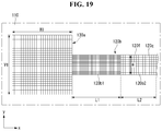
- the display device 100 may have a rectangular shape.
- a plurality of light source assemblies 140 may be installed in the display device 100 .
- Connectors 150 A, 150 B, 150 C, and 150 D may be disposed along a periphery of the display device 100 . That is, the connectors 150 A, 150 B, 150 C, and 150 D may be disposed along four sides of the display device 100 .
- the connectors 150 A, 150 B, 150 C, and 150 D may surround the plurality of light source assemblies 140 .
- the plurality of light source assemblies 140 may be electrically connected to the display device 100 .
- the connectors 150 A, 150 B, 150 C and 150 D may be electrically connected to the display device 100 .
- the connectors 150 A, 150 B, 150 C and 150 D may be connected to the plurality of light source assemblies 140 through the display device 100 .
- the connectors 150 A, 150 B, 150 C, and 150 D can transmit power supplied from a power supply unit to the light source assemblies 140 .
- the light source assemblies 140 can receive control signals transmitted from a controller through the connectors 150 A, 150 B, 150 C, and 150 D.
- an area in which the plurality of light source assemblies 140 are installed may be referred to as a display area F.
- an area in which the connectors 150 A, 150 B, 150 C, and 150 D are installed may be referred to as a bezel area G.
- the connectors 150 A, 150 B, 150 C, and 150 D may be disposed along four sides of the display device 100 to smoothly transmit the power and the control signals to the plurality of light source assemblies 140 .
- a ratio of the bezel area G can be increased and a ratio of the display area F can be reduced.
- the connectors 150 A and 150 C may be disposed along one side of the display device 100 and other side in parallel with the one side.
- the connectors 150 A and 150 C may include a left connector 150 A and a right connector 150 C, and the left connector 150 A and the right connector 150 C may be disposed opposite each other.
- the plurality of light source assemblies 140 may be disposed between the left connector 150 A and the right connector 150 C.
- the display area F may be disposed between the left connector 150 A and the right connector 150 C.
- the display area F may be disposed between the bezel areas G.
- the ratio of the bezel area G becomes smaller and the ratio of the display area F becomes larger. Therefore, it may be advantageous to display a large screen compared to an area of the display device 100 .
- the connector 150 A may be disposed along one side of the display device 100 .
- the light source assemblies 140 may be disposed in an area where the connector 150 A is not disposed.
- the connector 150 A disposed at the one side of the display device 100 can supply the power to all the light source assemblies 140 .
- the connector 150 A disposed at the one side of the display device 100 can transmit the control signals to all the light source assemblies 140 .
- the ratio of the bezel area G becomes smaller and the ratio of the display area F becomes larger. Therefore, it may be advantageous to display a large screen compared to the area of the display device 100 .
- an efficient connector 150 A structure or an efficient display device 100 wiring structure may be required in order to supply the power and transmit the control signal to the light source assemblies 140 through the relatively reduced connector 150 A.
- the display device 100 may include a base 110 .
- the base 110 may be referred to as a substrate 110 , a transparent substrate 110 , a plate 110 , or a transparent plate 110 .
- the base 110 may be made of a transparent material.
- the base 110 may have light transmission.
- a thickness of the base 110 may be very thin.
- the thickness of the base 110 may be 250 um.
- the base 110 may have insulating properties. The power supplied to the display device 100 can be blocked without passing through the base 110 .
- Heat may be applied to the base 110 during production process of the display device 100 .
- the base 110 may comprise a polyethylene terephthalate (PET) material.
- PET polyethylene terephthalate
- an electrode layer 120 may be formed on the base 110 .
- the electrode layer 120 may be referred to as an electrode 120 or a metal electrode 120 .
- the electrode layer 120 may have conductivity.
- the electrode layer 120 can function as a path for transmitting the power supplied from the power supply unit. Further, the electrode layer 120 can function as a path for transmitting the control signal transmitted from the controller.
- the electrode layer 120 may be coated on the base 110 .
- the electrode layer 120 may be coated on the base 110 with a very thin thickness.
- the electrode layer 120 may have light transmission due to its thin thickness. Therefore, even if the electrode layer 120 is coated on the base 110 , the display device 100 may have light transmission.
- the electrode layer 120 may form a pattern.
- the pattern of the electrode layer 120 can function as a wiring structure.
- the pattern of the electrode layer 120 may be formed through an additional process after the electrode layer 120 is coated on the base 110 .
- the pattern of the electrode layer 120 may be formed by irradiating a laser beam onto the electrode layer 120 coated on the base 110 .
- the pattern of the electrode layer 120 may be formed by etching the electrode layer 120 coated on the base 110 .
- the electrode layer 120 may include metal nano wires.
- the electrode layer 120 may include silver (Ag) nano wires.
- the silver (Ag) nano wires have high conductivity and can be excellent in light transmission.
- the electrode layer 120 may include silver.
- the electrode layer 120 may have a mesh shape formed of silver.
- the silver can have high conductivity.
- the electrode layer 120 may include copper.
- the electrode layer 120 may have a mesh shape formed of copper.
- the copper can have high conductivity.
- the electrode layer 120 may include nickel and chromium-plated copper.
- the electrode layer 120 may have a mesh shape formed of nickel and chromium-plated copper.
- the nickel and chromium-plated copper can have high conductivity.
- the electrode layer 120 may include copper oxide. Copper can be reddish and copper oxide can be black.
- the display device 100 may be grayed by including the copper oxide electrode layer 120 .
- a sheet resistance of the copper mesh electrode may be smaller than a sheet resistance of the silver mesh electrode.
- the sheet resistance of the silver mesh electrode may be smaller than a sheet resistance of the silver nano wires.
- the display device 100 may include a light source assembly 140 .
- the light source assembly 140 may be installed on the base 110 .
- the light source assembly 140 may be electrically connected to the electrode layer 120 .
- the electrode layer 120 may include a positive electrode 122 and a negative electrode 124 .
- the positive electrode 122 may be referred to as a positive electrode, an oxidation electrode, or an anode.
- the negative electrode 124 may be referred to as a negative electrode, a reduction electrode, or a cathode.
- the light source assembly 140 may be installed in a plurality of units.
- the plurality of light source assemblies 140 may be disposed along one side of the base 110 and may form one row.
- the plurality of light source assemblies 140 forming the one row may be spaced apart from each other.
- the plurality of light source assemblies 140 forming the one row may be disposed at regular intervals.
- a plurality of rows R 1 , R 2 , R 3 , R 4 , R 5 , and R 6 formed by the plurality of light source assemblies 140 may be formed.
- the rows R 1 , R 2 , R 3 , R 4 , R 5 , and R 6 each may be disposed along one side of the base 110 .
- the rows R 1 , R 2 , R 3 , R 4 , R 5 , and R 6 each may be spaced apart from each other.
- the rows R 1 , R 2 , R 3 , R 4 , R 5 , and R 6 each may be disposed at equal intervals from each other.
- the positive electrode 122 may extend along the one row.
- the positive electrode 122 may be electrically connected to each of the plurality of light source assemblies 140 in the one row.
- the positive electrode 122 may be located above the one row.
- the negative electrode 124 may extend along the one row.
- the negative electrode 124 may be electrically connected to each of the plurality of light source assemblies 140 in the one row.
- the negative electrode 124 may be located below the one row. That is, the one row may be located between the positive electrode 122 and the negative electrode 124 .
- the positive electrode 122 connected to the one row may be formed of one electrode.
- the plurality of light source assemblies 140 in the one row may be connected to one positive electrode 122 .
- the plurality of negative electrodes 124 connected to the one row may be formed.
- the negative electrode 124 may be formed to correspond to each of the plurality of light source assemblies 140 in the one row.
- a positive electrode 122 may be disposed between a first row R 1 and a second row R 2 .
- the positive electrode 122 may be disposed between a third row R 3 and a fourth row R 4 .
- the positive electrode 122 may be disposed between a fifth row R 5 and a sixth row R 6 .
- the positive electrode 122 may be disposed between a seventh row R 7 and an eighth row R 8 .
- Each of the plurality of light source assemblies 140 in the first row R 1 may be electrically connected to one positive electrode 122 disposed between the first row R 1 and the second row R 2 .
- Each of the plurality of light source assemblies 140 in the second row R 2 may be electrically connected to one positive electrode 122 disposed between the first row R 1 and the second row R 2 .
- a negative electrode 124 electrically connected to the first row R 1 may be disposed above the first row R 1 .
- the negative electrode 124 may be formed to correspond to each of the plurality of light source assemblies 140 in the first row R 1 .
- the negative electrode 124 electrically connected to the second row R 2 may be disposed below the second row R 2 .
- the negative electrode 124 may be formed to correspond to each of the plurality of light source assemblies 140 in the second row R 2 .
- a connection structure of the positive electrode 122 electrically connected to the third row R 3 and the fourth row R 4 , the negative electrode 124 electrically connected to the third row R 3 , and the negative electrode 124 electrically connected to the fourth row R 4 may be the same as the connection structure of the first row R 1 , the second row R 2 , the positive electrode 122 , and the negative electrode 124 described above.
- a connection structure of the fifth row R 5 and the sixth row R 6 and a connection structure of the seventh row R 7 and the eighth row R 8 may be the same as the connection structure of the first row R 1 and the second row R 2 .
- the light source assembly 140 may include a plurality of LED chips 140 a , 140 b , and 140 c .
- the light source assembly 140 may include at least one of a red LED chip 140 a , a green LED chip 140 b , and a blue LED chip 140 c .
- the light source assembly may be referred to as a light source or a chip.
- the LED chips may be referred to as chips.
- the plurality of light source assemblies 140 may be electrically connected to one positive electrode 122 , respectively.
- the negative electrodes 124 connected to the respective light source assemblies 140 may be independent of each other. Further, the negative electrode 124 electrically connected to the respective light source assemblies 140 may include three electrodes. The three electrodes may be electrically connected to the red LED chip 140 a , the green LED chip 140 b , and the blue LED chip 140 c , respectively. Thereby, the LED chips 140 a , 140 b , 140 c of the light source assembly 140 can be individually controlled.
- the light source assembly 140 may include at least one of a plurality of LED chips 140 a , 140 b , and 140 c or an IC chip 140 d .
- the IC chip may be referred to as a chip.
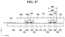
- the electrode layer 120 may include at least one of a positive electrode 122 , a negative electrode 124 , and a control electrode 125 .
- the positive electrode 122 may be referred to as an electrode.
- the negative electrode 124 may be referred to as an electrode.
- the control electrode 125 may be referred to as an electrode.
- the control electrode 125 may be referred to as a switching electrode.
- the control electrode 125 may electrically connect neighboring light source assemblies 140 to each other. In addition, the control electrode 125 may connect the neighboring light source assemblies 140 in series. The control electrode 125 may transmit a signal for controlling the IC chip 140 d of the light source assembly 140 .
- the plurality of light source assemblies 140 may be electrically connected to one positive electrode 122 , respectively.
- the negative electrodes 124 connected to the respective light source assemblies 140 may be independent of each other. Further, the negative electrode 124 electrically connected to the respective light source assemblies 140 may be one electrode. Even if the negative electrode 124 is not connected to each of the plurality of LED chips 140 a , 140 b , and 140 c included in the light source assembly 140 , the plurality of LED chips 140 a , 140 b and 140 c can be individually controlled through the IC chip 140 d.
- a current supplied through a power supply unit may flow in order of the positive electrode 122 , the plurality of LED chips 140 a , 140 b and 140 c , the IC chip 140 d and the negative electrode 12 .
- the current supplied through the power supply unit may flow in order of the positive electrode 122 , the IC chip 140 d , the plurality of LED chips 140 a , 140 b , 140 c , and the negative electrode 124 .
- an electrode layer 120 may include a first line 120 a or a second line 120 b .
- the first line 120 a may have a line width d 1 .
- the first line 120 a may be formed in a plurality.
- the plurality of first lines 120 a may be disposed at equal intervals P 1 .
- the second line 120 b may have a line width d 1 .
- the second line 120 b may be formed in a plurality.
- the plurality of second lines 120 b may be disposed at equal intervals P 1 .
- the plurality of first lines 120 a and the plurality of second lines 120 b may intersect each other.
- the plurality of first lines 120 a and the plurality of second lines 120 b may form a mesh shape.
- the plurality of first lines 120 a and the plurality of second lines 120 b may form a diamond structure.
- the plurality of first lines 120 a and the plurality of second lines 120 b may form a square or a rhombus.
- An angle formed by the first line 120 a and the second line 120 b may be A.
- A may be a right angle.
- an electrode layer 120 may include at least one of a first line 120 c , a second line 120 d , and a third line 120 e .
- the first line 120 c may extend along a longitudinal direction of the electrode layer 120 .
- the first line 120 c may have a line width d 1 .
- the first line 120 c may be formed in a plurality.
- the plurality of first lines 120 c may be disposed at equal intervals P 4 .
- the second line 120 d may have a line width d 1 .
- the second line 120 d may be formed in a plurality.
- the second line 120 d may connect neighboring first lines 120 c .
- the plurality of second lines 120 d may be disposed at equal intervals P 3 along the longitudinal direction of the electrode layer 120 .
- the plurality of first lines 120 c and the plurality of second lines 120 d may intersect with each other.
- the third line 120 e may be formed in a plurality.
- the third line 120 e may connect the neighboring first lines 120 c .
- a plurality of third lines 120 e may be disposed at equal intervals P 3 along the longitudinal direction of the electrode layer 120 .
- the plurality of first lines 120 c , the plurality of second lines 120 d , and the plurality of third lines 120 e may intersect with each other.
- the plurality of first lines 120 c , the plurality of second lines 120 d , and the plurality of third lines 120 e may form a mesh shape.
- the plurality of first lines 120 c , the plurality of second lines 120 d , and the plurality of third lines 120 e may form a brick structure.
- the plurality of first lines 120 c , the plurality of second lines 120 d , and the plurality of third lines 120 e may form a quadrangle.
- an electrode layer 120 may include a first line 120 f or a second line 120 g .
- the first line 120 f may extend along the longitudinal direction of the electrode layer 120 .
- the first line 120 f may have a line width d 1 .
- the first line 120 f may be formed in a plurality.
- the plurality of first lines 120 f may be disposed at equal intervals P 1 .
- the second line 120 g may have a line width d 1 .
- the second line 120 g may be formed in a plurality.
- the plurality of second lines 120 g may be disposed at equal intervals P 1 along the longitudinal direction of the electrode layer 120 .
- the plurality of first lines 120 f and the plurality of second lines 120 g may intersect with each other.
- the plurality of first lines 120 f and the plurality of second lines 120 g may be orthogonal.
- the plurality of first lines 120 f and the plurality of second lines 120 g may form a mesh shape.
- the plurality of first lines 120 f and the plurality of second lines 120 g may form a square structure.
- the plurality of first lines 120 f and the plurality of second lines 120 g may form a quadrangle or a square.
- An angle formed by the first line 120 f and the second line 120 g may be B.
- B may be a right angle.
- a sheet resistance of a diamond mesh shape and a sheet resistance of a square mesh shape may be the same.
- a path of the diamond mesh shape may be longer than a path of the square mesh shape. Therefore, the square mesh shape may have less power loss than the diamond mesh shape. Further, the transmittance of the diamond mesh shape may be higher than that of the square mesh shape.
- a sheet resistance of a brick mesh shape may be higher than that of the square mesh shape.
- the transmittance of the brick mesh shape may be substantially the same as the transmittance of the square mesh shape.
- a pad 130 a may be connected to one side of an electrode layer 120 a .
- the pad 130 a may be referred to as a metal pad 130 a .
- the pad 130 a may be physically or electrically connected to the electrode layer 120 a .
- a chip, a light source assembly, or an electronic component may be physically or electrically connected to the pad 130 a .
- a material of the pad 130 a may be the same as that of the electrode layer 120 a .
- the pad 130 a may have a horizontal line H 1 and a vertical line V 1 .
- a horizontal direction of the pad 130 a may be the same as a longitudinal direction of the electrode layer 120 a .
- the pad 130 a may be formed integrally with the electrode layer 120 a .
- the electrode layer 120 a may include a mesh shape.
- the pad 130 a may include a mesh shape.
- the mesh shape of the electrode layer 120 a and the mesh shape of the pad 130 a may be continuously connected.
- a density of the mesh shape of the electrode layer 120 a and a density of the mesh shape of the pad 130 a may be the same.
- the number of mesh-shaped openings of the electrode layer 120 a per unit area may be equal to the number of mesh-shaped openings of the pad 130 a per unit area.
- the electrode layer 120 a may have a width H.
- the width H of the electrode layer 120 a may be smaller than the vertical line V 1 of the pad 130 a .
- the electrode layer 120 a may be connected to a central part of the vertical line V 1 of the pad 130 a.
- the density of the mesh shape may mean the number of components per unit area.
- the density of the mesh shape may mean the number of lines forming a lattice per unit area.
- a pad 130 a and an electrode layer 120 a may be disconnected.
- a part where the pad 130 a and the electrode layer 120 a are connected may receive more impact and disconnection may easily occur.
- flexibility of a region where the pad 130 a is located and flexibility of a region where the pad 130 a is not located may be different from each other.
- the region where the pad 130 a is not located in the base 110 may be more flexible than the region where the pad 130 a is located. Therefore, the flexibility of the base 110 may be partially changed, and thus disconnection of the part where the pad 130 a and the electrode layer 120 a are connected may easily occur.
- an electrode layer 120 b may include a first region 120 b 1 or a second region 120 b 2 .
- the regions 120 b 1 and 120 b 2 may be referred to as parts 120 b 1 and 120 b 2 .
- the first region 120 b 1 may be located between a pad 130 a and the second region 120 b 2 .
- the pad 130 a may be physically or electrically connected to the first region 120 b 1 .
- One side of the first region 120 b 1 may be physically or electrically connected to the pad 130 a .
- Other side of the first region 120 b 1 may be physically or electrically connected to the second region 120 b 2 .
- the first region 120 b 1 may have a length L 1 .
- the second region 120 b 2 may have a length L 2 .
- a mesh shape of the pad 130 a and a mesh shape of the first region 120 b 1 may be continuously connected.
- a density of the mesh shape of the first region 120 b 1 may be higher than a density of the mesh shape of the pad 130 a .
- the density of the mesh shape of the first region 120 b 1 may be higher than a density of the mesh shape of the second region 120 b 2 .
- the density of the mesh shape of the second region 120 b 2 may be the same as the density of the mesh shape of the pad 130 a .
- the number of mesh-shaped openings of the first region 120 b 1 per unit area may be larger than the number of mesh-shaped openings of the pad 130 a per unit area.
- the number of mesh-shaped openings of the first region 120 b 1 per unit area may be larger than the number of mesh-shaped openings of the second region 120 b 2 per unit area.
- the number of mesh-shaped openings of the pad 130 a per unit area may be the same as the number of mesh-shaped openings of the second area 120 b 2 .
- the length L 2 may be greater than the length L 1 .
- the length L 1 may be less than the length H 1 .
- the length L 1 may be substantially equal to or greater than the length H 1 .
- connection strength between the pad 130 a and the first region 120 b 1 can be increased.
- the number of first lines 120 f connected to the pad 130 a may be larger than that of FIG. 17 . Therefore, in contrast to the case of FIG. 17 , the disconnection between the pad 130 a and the electrode layer 120 b can be reduced.
- an electrode layer 120 c may include a first region 120 c 1 or a second region 120 c 2 .
- the regions 120 c 1 and 120 c 2 may be referred to as parts 120 c 1 and 120 c 2 .
- the first region 120 c 1 may be located between a pad 130 a and the second region 120 c 2 .
- the pad 130 a may be physically or electrically connected to the first region 120 c 1 .
- One side of the first region 120 c 1 may be physically or electrically connected to the pad 130 a .
- Other side of the first region 120 c 1 may be physically or electrically connected to the second region 120 c 2 .
- the first region 120 c 1 may have a length L 3 .
- the second region 120 c 2 may have a length L 4 .
- a vertical length of the one side of the first region 120 c 1 may be V 1
- a vertical length of other side of the first region 120 c 1 may be H.
- the length V 1 may be greater than the length H.
- the vertical length of the first region 120 c 1 may be reduced from the one side of the first region 120 c 1 to the other side of the first region 120 c 1 .
- a mesh shape of the pad 130 a , a mesh shape of the first area 120 c 1 , and a mesh shape of the second area 120 c 2 may be continuously connected.
- the mesh shape of the pad 130 a , the mesh shape of the first region 120 c 1 , and the mesh shape of the second region 120 c 2 may be the same in a density.
- the number of mesh-shaped openings of the pad 130 a per unit area, the number of mesh-shaped openings of the first region 120 c 1 per unit area, and the number of openings of the mesh-shaped portion of the second region 120 c 2 per unit area may be equal to each other.
- the length L 3 may be greater than the length L 4 .
- the length L 3 may be less than the length H 1 .
- the length L 3 may be substantially equal to or greater than the length H 1 .
- the longer the length L 3 the higher the connection strength between the pad 130 a and the first region 120 c 1 .
- the number of first lines 120 f connected to the pad 130 a may be larger than that of FIG. 17 . Therefore, in contrast to the case of FIG. 17 , disconnection between the pad 130 a and the electrode layer 120 c may be reduced.
- an electrode layer 120 d may include a first region 120 d 1 or a second region 120 d 2 .
- the regions 120 d 1 and 120 d 2 may be referred to as parts 120 d 1 and 120 d 2 .
- the first region 120 d 1 may be located between a pad 130 a and the second region 120 d 2 .
- the pad 130 a may be physically or electrically connected to the first region 120 d 1 .
- One side of the first region 120 d 1 may be physically or electrically connected to the pad 130 a .
- Other side of the first region 120 d 1 may be physically or electrically connected to the second region 120 d 2 .
- the first region 120 d 1 may have a length L 3 .
- the second region 120 d 2 may have a length L 4 .
- a vertical length of the one side of the first region 120 d 1 may be V 1 and a vertical length of the other side of the first region 120 d 1 may be H.
- the length V 1 may be greater than the length H.
- the vertical length of the first region 120 d 1 may be reduced from the one side of the first region 120 d 1 to the other side of the first region 120 d 1 .
- a mesh shape of the pad 130 a and a mesh shape of the first region 120 d 1 may be continuously connected.
- a density of the mesh shape of the first region 120 d 1 may be higher than a density of the mesh shape of the pad 130 a .
- the density of the mesh shape of the first region 120 d 1 may be higher than a density of the mesh shape of the second region 120 d 2 .
- the density of the mesh shape of the second region 120 d 2 may be the same as the density of the mesh shape of the pad 130 a .
- the number of mesh-shaped openings of the first region 120 d 1 per unit area may be larger than the number of mesh-shaped openings of the pad 130 a per unit area.
- the number of mesh-shaped openings of the first area 120 d 1 per unit area may be larger than the number of mesh-shaped openings of the second area 120 d 2 per unit area.
- the number of mesh-shaped openings of the pad 130 a per unit area may be the same as the number of mesh-shaped openings of the second area 120 d 2 per unit area.
- the length L 4 may be greater than the length L 3 .
- the length L 3 may be less than the length H 1 .
- the length L 3 may be substantially equal to or greater than the length H 1 .
- the longer the length L 3 the higher the connection strength between the pad 130 a and the first region 120 d 1 .
- the number of first lines 120 f connected to the pad 130 a may be larger than that of FIG. 17 . Therefore, in contrast to the case of FIG. 17 , disconnection between the pad 130 a and the electrode layer 120 d may be reduced.
- a pad 130 b may be connected to one side of an electrode layer 120 a .
- the pad 130 b may be referred to as a metal pad 130 b .
- the pad 130 b may be physically or electrically connected to the electrode layer 120 a .
- a chip, a light source assembly, or an electronic component may be physically or electrically connected to the pad 130 b .
- a material of the pad 130 b may be the same as a material of the electrode layer 120 a .
- the pad 130 b may have a horizontal line H 1 and a vertical line V 1 .
- a horizontal direction of the pad 130 b may be the same as a longitudinal direction of the electrode layer 120 a .
- the pad 130 b may be formed integrally with the electrode layer 120 a .
- the electrode layer 120 a may include a mesh shape.
- the pad 130 b may include a mesh shape.
- the mesh shape of the electrode layer 120 a and the mesh shape of the pad 130 b may be continuously connected.
- a density of the mesh shape of the pad 130 b may be higher than a density of the mesh shape of the electrode layer 120 a .
- the number of mesh-shaped openings of the electrode layer 120 a per unit area may be smaller than the number of mesh-shaped openings of the pad 130 b unit area.
- the electrode layer 120 a may have a width H.
- the width H of the electrode layer 120 a may be smaller than the vertical line V 1 of the pad 130 b .
- the electrode layer 120 a may be connected to a center part of the vertical line V 1 of the pad 130 b.
- an electrode layer 120 b may include a first region 120 b 1 or a second region 120 b 2 .
- the regions 120 b 1 and 120 b 2 may be referred to as parts 120 b 1 and 120 b 2 .
- the first region 120 b 1 may be located between a pad 130 b and the second region 120 b 2 .
- the pad 130 b may be physically or electrically connected to the first region 120 b 1 .
- One side of the first region 120 b 1 may be physically or electrically connected to the pad 130 b .
- Other side of the first region 120 b 1 may be physically or electrically connected to the second region 120 b 2 .
- the first region 120 b 1 may have a length L 1 .
- the second region 120 b 2 may have a length L 2 .
- a mesh shape of the pad 130 b and a mesh shape of the first region 120 b 1 may be continuously connected.
- a density of the mesh shape of the first region 120 b 1 may be the same as a density of the mesh shape of the pad 130 b .
- the density of the mesh shape of the first region 120 b 1 may be higher than a density of the mesh shape of the second region 120 b 2 .
- the density of the mesh shape of the pad 130 b may be higher than the density of the mesh shape of the second region 120 b 2 .
- the number of mesh-shaped openings of the first region 120 b 1 per unit area may be equal to the number of mesh-shaped openings of the pad 130 b per unit area.
- the number of mesh-shaped openings of the first area 120 b 1 per unit area may be larger than the number of mesh-shaped openings of the second area 120 b 2 per unit area.
- the number of mesh-shaped openings of the pad 130 b per unit area may be larger than the number of mesh-shaped openings of the second area 120 b 1 per unit area.
- the length L 2 may be greater than the length L 1 .
- the length L 1 may be less than the length H 1 .
- the length L 1 may be substantially equal to or greater than the length H 1 .
- the longer the length L 1 the higher the connection strength between the pad 130 b and the first region 120 b 1 .
- the number of first lines 120 f connected to the pad 130 b may be larger than that of FIG. 22 . Accordingly, in contrast to the case of FIG. 22 , disconnection of the pad 130 b and the electrode layer 120 b may be reduced.
- an electrode layer 120 c may include a first region 120 c 1 or a second region 120 c 2 .
- the regions 120 c 1 and 120 c 2 may be referred to as parts 120 c 1 and 120 c 2 .
- the first region 120 c 1 may be located between a pad 130 b and the second region 120 c 2 .
- the pad 130 b may be physically or electrically connected to the first region 120 c 1 .
- One side of the first region 120 c 1 may be physically or electrically connected to the pad 130 b .
- Other side of the first region 120 c 1 may be physically or electrically connected to the second region 120 c 2 .
- the first region 120 c 1 may have a length L 3 .
- the second region 120 c 2 may have a length L 4 .
- a vertical length of the one side of the first region 120 c 1 may be V 1
- a vertical length of the other side of the first region 120 c 1 may be H.
- the length V 1 may be greater than the length H.
- the vertical length of the first region 120 c 1 may be reduced from the one side of the first region 120 c 1 to the other side of the first region 120 c 1 .
- a mesh shape of the pad 130 b , a mesh shape of the first region 120 c 1 , and a mesh shape of the second region 120 c 2 may be continuously connected.
- a density of the mesh shape of the pad 130 b may be higher than a density of the mesh shape of the electrode layer 120 c .
- the mesh shape of the first region 120 c 1 and the mesh shape of the second region 120 c 2 may be the same.
- the number of mesh-shaped openings of the pad 130 b per unit area may be larger than the number of mesh-shaped openings of the electrode layer 120 c per unit area.
- the number of mesh-shaped openings of the pad 130 b per unit area, the number of mesh-shaped openings of the first region 120 c 1 per unit area, and the number of mesh-shaped openings of the second region 120 c 2 per unit area may be equal to each other.
- the length L 3 may be greater than the length L 4 .
- the length L 3 may be less than the length H 1 .
- the length L 3 may be substantially equal to or greater than the length H 1 .
- the longer the length L 3 the higher the connection strength between the pad 130 b and the first region 120 c 1 .
- the number of first lines 120 f connected to the pad 130 b may be larger than that of FIG. 22 . Accordingly, in contrast to the case of FIG. 22 , disconnection of the pad 130 b and the electrode layer 120 c may be reduced.
- an electrode layer 120 d may include a first region 120 d 1 or a second region 120 d 2 .
- the regions 120 d 1 and 120 d 2 may be referred to as parts 120 d 1 and 120 d 2 .
- the first region 120 d 1 may be located between a pad 130 b and the second region 120 d 2 .
- the pad 130 b may be physically or electrically connected to the first region 120 d 1 .
- One side of the first region 120 d 1 may be physically or electrically connected to the pad 130 b .
- Other side of the first region 120 d 1 may be physically or electrically connected to the second region 120 d 2 .
- the first region 120 d 1 may have a length L 3 .
- the second region 120 d 2 may have a length L 4 .
- a vertical length of the one side of the first region 120 d 1 may be V 1 and a vertical length of the other side may be H.
- the length V 1 may be greater than the length H.
- the vertical length of the first region 120 d 1 may be reduced from the one side of the first region 120 d 1 to the other side of the first region 120 d 1 .
- a mesh shape of the pad 130 b and a mesh shape of the first region 120 d 1 may be continuously connected.
- a density of the mesh shape of the first region 120 d 1 may be the same as a density of the mesh shape of the pad 130 b .
- the density of the mesh shape of the first region 120 d 1 may be higher than a density of the mesh shape of the second region 120 d 2 .
- the number of mesh-shaped openings of the first region 120 d 1 per unit area may be equal to the number of mesh-shaped openings of the pad 130 b per unit area.
- the number of mesh-shaped openings of the first area 120 d 1 per unit area may be larger than the number of mesh-shaped openings of the second area 120 d 2 per unit area.
- the length L 4 may be greater than the length L 3 .
- the length L 3 may be less than the length H 1 .
- the length L 3 may be substantially equal to or greater than the length H 1 .
- the connection strength between the pad 130 b and the first region 120 d 1 can be increased.
- the number of first lines 120 f connected to the pad 130 b may be larger than that of FIG. 22 . Accordingly, in contrast to the case of FIG. 22 , disconnection of the pad 130 b and the electrode layer 120 d may be reduced.
- a pad 130 c may be connected to one side of an electrode layer 120 a .
- the pad 130 c may be referred to as a metal pad 130 c .
- the pad 130 c may be a metal film or a metal thin film formed on a base 110 .
- the pad 130 c may be a film containing a copper material.
- the pad 130 c may be physically or electrically connected to the electrode layer 120 a .
- a chip, a light source assembly, or an electronic component may be physically or electrically connected to the pad 130 c .
- a material of the pad 130 c may be the same as that of the electrode layer 120 a .
- the pad 130 c may have a horizontal line H 1 and a vertical line V 1 .
- a horizontal direction of the pad 130 c may be the same as a longitudinal direction of the electrode layer 120 a .
- the pad 130 c may be formed integrally with the electrode layer 120 a .
- the electrode layer 120 a may include a mesh shape.
- the mesh shape of the electrode layer 120 a and the pad 130 c may be continuously connected.
- a density of the mesh shape of the electrode layer 120 a may be uniform.
- the number of mesh-shaped openings of the electrode layer 120 a per unit area may be kept the same throughout the electrode layer.
- the electrode layer 120 a may have a width H.
- the width H of the electrode layer 120 a may be smaller than the vertical line V 1 of the pad 130 c .
- the electrode layer 120 a may be connected to a center part of the vertical line V 1 of the pad 130 c.
- a pad 130 c and an electrode layer 120 a may be disconnected.
- a part where the pad 130 c and the electrode layer 120 a are connected may receive more impact, and disconnection may easily occur.
- flexibility of a region where the pad 130 c is located and flexibility of a region where the pad 130 c is not located in the base 110 may be different from each other.
- the region where the pad 130 c is not located may be more flexible than the region where the pad 130 c is located. Accordingly, the flexibility of the base 110 may be partially varied, and thus the disconnection of the part where the pad 130 c and the electrode layer 120 a are connected may easily occur.
- an electrode layer 120 b may include a first region 120 b 1 or a second region 120 b 2 .
- the regions 120 b 1 and 120 b 2 may be referred to as parts 120 b 1 and 120 b 2 .
- the first region 120 b 1 may be located between a pad 130 c and the second region 120 b 2 .
- the pad 130 c may be physically or electrically connected to the first region 120 b 1 .
- One side of the first region 120 b 1 may be physically or electrically connected to the pad 130 c .
- Other side of the first region 120 b 1 may be physically or electrically connected to the second region 120 b 2 .
- the first region 120 b 1 may have a length L 1 .
- the second region 120 b 2 may have a length L 2 .
- a density of a mesh shape of the first region 120 b 1 may be higher than a density of a mesh shape of the second region 120 b 2 .
- the density of the mesh shape of the second region 120 b 2 may be the same as a density of a mesh shape of the pad 130 c .
- the number of mesh-shaped openings of the first region 120 b 1 per unit area may be larger than the number of mesh-shaped openings of the second region 120 b 2 per unit area.
- the number of mesh-shaped openings of the pad 130 c per unit area may be the same as the number of mesh-shaped openings of the second area 120 b 2 per unit area.
- the length L 2 may be greater than the length L 1 .
- the length L 1 may be less than the length H 1 .
- the length L 1 may be substantially equal to or greater than the length H 1 .
- the connection strength between the pad 130 c and the first region 120 b 1 can be increased.
- the number of first lines 120 f connected to the pad 130 c may be larger than that of FIG. 26 . Accordingly, in contrast to the case of FIG. 26 , disconnection of the pad 130 c and the electrode layer 120 b may be reduced.
- an electrode layer 120 c may include a first region 120 c 1 or a second region 120 c 2 .
- the regions 120 c 1 and 120 c 2 may be referred to as parts 120 c 1 and 120 c 2 .
- the first region 120 c 1 may be located between a pad 130 c and the second region 120 c 2 .
- the pad 130 c may be physically or electrically connected to the first region 120 c 1 .
- One side of the first region 120 c 1 may be physically or electrically connected to the pad 130 c .
- Other side of the first region 120 c 1 may be physically or electrically connected to the second region 120 c 2 .
- the first region 120 c 1 may have a length L 3 .
- the second region 120 c 2 may have a length L 4 .
- a vertical length of the one side of the first region 120 c 1 may be V 1
- a vertical length of the other side of the first region 120 c 1 may be H.
- the length V 1 may be greater than the length H.
- the vertical length of the first region 120 c 1 may be reduced from the one side of the first region 120 c 1 to the other side of the first region 120 c 1 .
- a mesh shape of the first region 120 c 1 and a mesh shape of the second region 120 c 2 may be the same.
- the number of mesh-shaped openings of the first region 120 c 1 per unit area and the number of the mesh-shaped openings of the second region 120 c 2 per unit area may be equal to each other.
- the length L 3 may be greater than the length L 4 .
- the length L 3 may be less than the length H 1 .
- the length L 3 may be substantially equal to or greater than the length H 1 .
- the longer the length L 3 the higher the connection strength between the pad 130 c and the first region 120 c 1 .
- the number of first lines 120 f connected to the pad 130 c may be larger than that of FIG. 26 . Accordingly, in contrast to the case of FIG. 26 , disconnection of the pad 130 c and the electrode layer 120 c may be reduced.
- an electrode layer 120 d may include a first region 120 d 1 or a second region 120 d 2 .
- the regions 120 d 1 and 120 d 2 may be referred to as parts 120 d 1 and 120 d 2 .
- the first region 120 d 1 may be located between a pad 130 c and the second region 120 d 2 .
- the pad 130 c may be physically or electrically connected to the first region 120 d 1 .
- One side of the first region 120 d 1 may be physically or electrically connected to the pad 130 c .
- Other side of the first region 120 d 1 may be physically or electrically connected to the second region 120 d 2 .
- the first region 120 d 1 may have a length L 3 .
- the second region 120 d 2 may have a length L 4 .
- a vertical length of the one side of the first area 120 d 1 may be V 1 and a vertical length of the other side may be H.
- the length V 1 may be greater than the length H.
- the vertical length of the first region 120 d 1 may be reduced from the one side of the first region 120 d 1 to the other side of the first region 120 d 1 .
- a density of a mesh shape of the first region 120 d 1 may be higher than a density of a mesh shape of the second region 120 d 2 .
- the number of mesh-shaped openings of the first region 120 d 1 per unit area may be larger than the number of mesh-shaped openings of the second region 120 d 2 per unit area.
- the length L 4 may be greater than the length L 3 .
- the length L 3 may be less than the length H 1 .
- the length L 3 may be substantially equal to or greater than the length H 1 .
- the longer the length L 3 the higher the connection strength between the pad 130 c and the first region 120 d 1 .
- the number of first lines 120 f connected to the pad 130 c may be larger than that of FIG. 26 . Accordingly, in contrast to the case of FIG. 26 , disconnection of the pad 130 c and the electrode layer 120 d may be reduced.
- a pad 130 g may be surrounded by pads 130 d , 130 e , and 130 f .
- a first part 122 a 5 may be physically or electrically connected to the pads 130 d , 130 e , and 130 f .
- a second part 122 a 2 may be physically or electrically connected to the pad 130 g .
- a third part 122 a 1 may physically or electrically connect the pads 130 d and 130 g .
- a fourth part 122 a 3 may physically or electrically connect the pads 130 e and 130 g .
- a fifth part 122 a 4 may physically or electrically connect the pads 130 f and 130 g .
- LED chips 140 a , 140 b , and 140 c may be physically or electrically connected to the pads 130 d , 130 e , and 130 f .
- An IC chip 140 d may be physically or electrically connected to the pad 130 g .
- a positive electrode 122 a may include at least one of the first part 122 a 5 to the fifth part 122 a 4 .
- the positive electrode 122 a may include a mesh shape.
- a region 110 g where the mesh shape is not formed may be located between the second part 122 a 2 and the third part 122 a 1 .
- the region 110 g where the mesh shape is not formed may be located between the second part 122 a 2 and the pas 130 d .
- a region 110 f where the mesh shape is not formed may be located between the second part 122 a 2 and the fourth part 122 a 3 .
- the region 110 f where the mesh shape is not formed may be located between the second part 122 a 2 and the pad 130 e .
- a region 110 e where the mesh shape is not formed may be located between the fourth part 122 a 3 and the fifth part 122 a 4 .
- the region 110 e where the mesh shape is not formed may be located between the pads 130 e and 130 f.
- One side of a first part 125 a 1 may be physically or electrically connected to the pad 130 g .
- One side of a second part 125 a 2 may be physically or electrically connected to the pad 130 g .
- a control electrode 125 a may include the first part 125 a 1 or the second part 125 a 2 .
- a first part 124 a 1 may face the control electrode 125 a .
- a second part 124 a 2 may extend from the first part 124 a 1 and may be physically or electrically connected to the pad 130 g .
- a negative electrode 124 a may include the first part 124 a 1 or the second part 124 a 2 .
- a region 110 a where the mesh shape is not formed may be located between the parts 122 a 1 and 125 a 1 .
- the region 110 a where the mesh shape is not formed may be located between the parts 122 a 5 and 125 a 1 .
- the region 110 a where the mesh shape is not formed may be located between the parts 125 a 1 and the pad 130 d .
- a region 110 d where the mesh shape is not formed may be located between the parts 122 a 4 and 125 a 2 .
- the region 110 d where the mesh shape is not formed may be located between the parts 122 a 5 and 125 a 2 .
- the region 110 d where the mesh shape is not formed may be located between the part 125 a 2 and the pad 130 f .
- a region 110 b where the mesh shape is not formed may be located between the parts 125 a 1 and 124 a 2 .
- the region 110 b where the mesh shape is not formed may be located between the parts 125 a 1 and 124 a 1 .
- a region 110 c where the mesh shape is not formed may be located between the parts 125 a 2 and 124 a 2 .
- the region 110 c where the mesh shape is not formed may be located between the parts 125 a 2 and 124 a 1 .
- a pad 130 g may be surrounded by pads 130 d , 130 e , and 130 f .
- a first part 122 b 8 may be adjacent to the pads 130 d , 130 e , and 130 f and may surround the pads 130 d , 130 e , and 130 f .
- a second part 122 b 2 may physically or electrically connect the pads 130 d and 130 g .
- a third part 122 b 1 may physically or electrically connect the first part 122 b 8 and the pad 130 d .
- a fourth part 122 b 3 may physically or electrically connect the pad 130 g and the first part 122 b 8 .
- a fifth part 122 b 4 may physically or electrically connect the pads 130 g and 130 e .
- a sixth part 122 b 5 may physically or electrically connect the pad 130 e and the first part 122 b 8 .
- a seventh part 122 b 6 may physically or electrically connect the pads 130 g and 130 f .
- An eighth part 122 b 7 may physically or electrically connect the pad 130 f and the first part 122 b 8 .
- a positive electrode 122 b may include at least one of the first part 122 b 8 to the eighth part 122 b 7 .
- the positive electrode 122 b may include a mesh shape.
- a region 110 g where the mesh shape is not formed may be located between the second part 122 b 2 and the fourth part 122 b 3 .
- the region 110 g where the mesh shape is not formed may be located between the first part 122 b 8 and the pad 130 d .
- a region 110 f where the mesh shape is not formed may be located between the fourth part 122 b 3 and the fifth part 122 b 4 .
- the region 110 f where the mesh shape is not formed may be located between the fourth part 122 b 3 and the pad 130 e .
- a region 110 e where the mesh shape is not formed may be located between the fifth part 122 b 4 and the seventh part 122 b 6 .
- the region 110 e where the mesh shape is not formed may be located between the pads 130 e and 130 f
- One side of a first part 125 b 1 may be physically or electrically connected to a second part 125 b 2 .
- the second part 125 b 2 may be physically or electrically connected to the first part 125 b 1 and the pad 130 g .
- One side of a fourth part 125 b 4 may be physically or electrically connected to a third part 125 b 3 .
- the third part 125 b 3 may be physically or electrically connected to the fourth part 125 b 4 and the pad 130 g .
- a control electrode 125 b may include at least one of the first part 125 b 1 to the fourth part 125 b 4 .
- a first part 124 b 1 may face the control electrode 125 b .
- a second part 124 b 2 may extend from the first part 124 b 1 and may be physically or electrically connected to the pad 130 g .
- a negative electrode 124 b may include the first part 124 b 1 or the second part 124 b 2 .
- a region 110 a where the mesh shape is not formed may be located between the parts 122 b 1 and 125 b 1 .
- the region 110 a where the mesh shape is not formed may be located between the parts 122 b 2 and 125 b 2 .
- the region 110 a where the mesh shape is not formed may be located between the part 125 b 1 and the pad 130 d .
- a region 110 d where the mesh shape is not formed may be located between the parts 122 b 8 and 125 b 4 .
- the region 110 d where the mesh shape is not formed may be located between the parts 122 b 6 and 125 b 3 .
- the region 110 d where the mesh shape is not formed may be located between the part 125 b 3 and the pad 130 f .
- a region 110 b where the mesh shape is not formed may be located between the parts 125 b 1 and 124 b 1 .
- the region 110 b where the mesh shape is not formed may be located between the parts 125 b 2 and 124 b 2 .
- a region 110 c where the mesh shape is not formed may be located between the parts 125 b 4 and 124 b 1 .
- the region 110 c where the mesh shape is not formed may be located between the parts 125 b 3 and 124 b 2 .
- Densities of the mesh shapes of the parts 122 b 8 , 125 b 1 , 125 b 4 , and 124 b 1 may be the same.
- the number of openings of the mesh shape of the parts 122 b 8 , 125 b 1 , 125 b 4 , and 124 b 1 per unit area may be equal to each other.
- Densities of the mesh shapes of the parts 122 b 1 , 122 b 2 , 122 b 3 , 122 b 4 , 122 b 5 , 122 b 6 , 122 b 7 , 125 b 2 , 125 b 3 , and 124 b 2 may be the same.
- the number of openings of the mesh shape of the parts 122 b 1 , 122 b 2 , 122 b 3 , 122 b 4 , 122 b 5 , 122 b 6 , 122 b 7 , 125 b 2 , 125 b 3 , 124 b 2 per unit area may be equal to each other.
- the densities of the mesh shapes of the parts 122 b 1 , 122 b 2 , 122 b 3 , 122 b 4 , 122 b 5 , 122 b 6 , 122 b 7 , 125 b 2 , 125 b 3 and 124 b 2 may be higher than the densities of the mesh shapes of the parts 122 b 8 , 125 b 1 , 125 b 4 and 124 b 1 .
- the number of openings of the mesh shape of the parts 122 b 1 , 122 b 2 , 122 b 3 , 122 b 4 , 122 b 5 , 122 b 6 , 122 b 7 , 125 b 2 , 125 b 3 , and 124 b 2 per unit area may be greater than the number of openings of the mesh shape of the parts 122 b 8 , 125 b 1 , 125 b 4 , and 124 b 1 per unit area.
- the number of a first line 120 h or a second line 120 i connected to the pads 130 d , 130 e , 130 f , and 130 g may be larger than that in the case of FIG. 31 . Therefore, in contrast to the case of FIG. 31 , disconnection of the pads 130 d , 130 e , 130 f , and 130 g and the electrode layers 122 b , 125 b , and 124 b may be reduced.
- a ninth part 122 c 4 may physically or electrically connect a third part 122 b 1 , a fourth part 122 b 3 , and a sixth part 122 b 5 .
- a tenth part 122 c 7 may physically or electrically connect the sixth part 122 b 5 and an eighth part 122 b 7 .
- a positive electrode 122 c may include at least one of a first part 122 b 8 to the tenth part 122 c 7 .
- Densities of mesh shapes of the parts 122 c 4 and 122 c 7 may be equal to each other. Alternatively, the number of openings of the mesh shape of the parts 122 c 4 and 122 c 7 per unit area may be equal to each other. The densities of the mesh shapes of the parts 122 c 4 and 122 c 7 may be higher than densities of the mesh shapes of parts 122 b 8 , 125 b 1 , 125 b 4 and 124 b 1 .
- the number of openings of the mesh shape of the parts 122 c 4 , 122 c 7 per unit area may be larger than the number of openings of the mesh shape of the parts 122 b 8 , 125 b 1 , 125 b 4 , and 124 b 1 per unit area.
- the number of a first line 120 h or a second line 120 i connected to the pads 130 d , 130 e , 130 f , and 130 g may be larger than that in the case of FIG. 31 . Therefore, in contrast to the case of FIG. 31 , disconnection of the pads 130 d , 130 e , 130 f , and 130 g and electrode layers 122 c , 125 b , and 124 b may be reduced.
- a second part 122 d 2 may physically or electrically connect pads 130 d and 130 g .
- a third part 122 d 1 may physically or electrically connect a first part 122 b 8 and the pad 130 d .
- a fourth part 122 d 3 may be physically or electrically connected to the pad 130 g .
- a ninth part 122 d 4 may be located between the first part 122 b 8 and the fourth part 122 d 3 and may physically or electrically connect the first part 122 b 8 to the fourth part 122 d 3 .
- a fifth part 122 d 5 may be located between the pad 130 g and a pad 130 e and may physically or electrically connect the pad 130 g to the pad 130 e .
- a sixth part 122 d 6 may physically or electrically connect the first part 122 b 8 and the pad 130 e .
- a seventh part 122 d 7 may be located between the pad 130 g and a pad 130 f and may physically or electrically connect the pad 130 g to the pas 130 f .
- An eighth part 122 d 8 may be located between the first part 122 b 8 and the pad 130 f and may physically or electrically connect the first part 122 b 8 to the pad 130 f .
- a tenth part 122 d 9 may physically or electrically connect the sixth part 122 d 6 and the eighth part 122 d 8 .
- a positive electrode 122 d may include at least one of the first to tenth parts.
- the second part 122 d 2 to the tenth part 122 d 9 may be a metal film or a metal thin film formed on a base 110 instead of a mesh shape.
- the second part 122 d 2 to the tenth part 122 d 9 may be a film containing a copper material.
- the positive electrode 122 d may include a mesh shape.
- a region 110 g where the mesh shape is not formed may be located between the second part 122 d 2 and the fourth part 122 d 3 .
- the region 110 g where the mesh shape is not formed may be located between the ninth part 122 d 4 and the pad 130 d .
- a region 110 f where the mesh shape is not formed may be located between the fourth part 122 d 3 and the fifth part 122 d 5 .
- the region 110 f where the mesh shape is not formed may be located between the fourth part 122 d 3 and the pad 130 e .
- a region area 110 e where the mesh shape is not formed may be located between the fifth part 122 d 5 and the seventh part 122 d 7 .
- the region 110 e where the mesh shape is not formed may be located between the pads 130 e and 130 f.
- One side of a first part 125 d 1 may be physically or electrically connected to a second part 125 d 2 .
- the second part 125 d 2 may be physically or electrically connected to the first part 125 d 1 and the pad 130 g .
- One side of a fourth part 125 d 4 may be physically or electrically connected to a third part 125 d 3 .
- the third part 125 d 3 may be physically or electrically connected to the fourth part 125 d 4 and the pad 130 g .
- a control electrode 125 d may include at least one of the first part 125 d 1 to the fourth part 125 d 4 .
- a first part 124 d 1 may face the control electrode 125 d .
- a second part 124 d 2 may extend from the first part 124 d 1 and may be physically or electrically connected to the pad 130 g .
- a negative electrode 124 d may include the first part 124 d 1 or the second part 124 d 2 .
- a region 110 a where the mesh shape is not formed may be located between the parts 122 d 2 and 125 d 2 .
- the region 110 a where the mesh shape is not formed may be located between the parts 122 d 1 and 125 d 1 .
- the region 110 a where the mesh shape is not formed may be located between the part 125 d 2 and the pad 130 d .
- a region 110 d where the mesh shape is not formed may be located between the parts 122 d 7 and 125 d 3 .
- the region 110 d where the mesh shape is not formed may be located between the parts 122 d 8 and 125 d 4 .
- the region 110 d where the mesh shape is not formed may be located between the part 125 d 3 and the pad 130 f .
- a region 110 b where the mesh shape is not formed may be located between the parts 125 d 1 and 124 d 1 .
- the region 110 b where the mesh shape is not formed may be located between the parts 125 d 2 and 124 d 2 .
- a region 110 c where the mesh shape is not formed may be located between the parts 125 d 4 and 124 d 1 .
- the region area 110 c where the mesh shape is not formed may be located between the parts 125 d 3 and 124 d 2 .
- the parts 125 d 2 , 124 d 2 , and 125 d 3 may be a metal film or a metal thin film formed on the base 110 instead of a mesh shape.
- the parts 125 d 2 , 124 d 2 , and 125 d 3 may be a film containing a copper material.
- the number of a first line 120 h or a second line 120 i connected to the parts 122 d 1 , 122 d 2 , 122 d 3 , 122 d 4 , 122 d 5 , 122 d 6 , 122 d 7 , 122 d 8 , 122 d 9 , 125 d 2 , 125 d 3 , and 124 d 2 may be greater than the number of the first line 120 h or the second line 120 i connected to the pads 130 d , 130 e , 130 f , and 130 g . Therefore, in contrast to the case of FIG. 31 , disconnection of the electrode layers 122 d , 125 d , and 124 d may be reduced.
- a pad 130 may be formed as a part of an electrode layer 120 .
- the pad 130 may be formed in a plurality.
- a solder 135 may be formed on the pad 130 .
- the solder 135 may attach a light source assembly 140 or an FPCB 150 to the pad 130 .
- the solder 135 may include an epoxy.
- the epoxy can improve strength of the solder 135 .
- the solder 135 may be formed by a low temperature reflow process. For example, the low temperature reflow process may proceed at 160 degrees. Since a base 110 , the electrode layer 120 , and the pad 130 have high melting points, there is no change in the state at 160 degrees.
- the FPCB 150 may physically or electrically connect the electrode layer 120 to an external circuit.
- an adhesive layer 160 may be formed on the base 110 .
- the electrode layer 120 may be located between the base 110 and the adhesive layer 160 .
- the adhesive layer 160 may include optical clear adhesive (OCA).
- OCA optical clear adhesive
- the adhesive layer 160 may be silicon, acrylic, or a combination thereof.
- the adhesive layer 160 may include a hole 160 a .
- the light source assembly 140 may be located in the hole 160 a .
- a height of the adhesive layer 160 may be higher than a height of the light source assembly 140 .
- the height of the adhesive layer 160 may be 500 ⁇ m or more to 800 ⁇ m or less.
- a width OWT of the hole 160 a may be larger than a width DWT of the light source assembly 140 .
- a protective layer 170 may be located on the adhesive layer 160 .
- the protective layer 170 can prevent the adhesive layer 160 from being exposed to the outside and the protective layer 170 can preserve an adhesive force of the adhesive layer 160 .
- the protective layer 170 may be separated from the adhesive layer 160 as needed.
- resin 180 may be applied to the base 110 , the electrode layer 120 , the FPCB 150 , and the light source assembly 140 .
- a primer process may be performed on the electrode layer 120 for adhesion between the resin 180 and the electrode layer 120 .
- a thermosetting or photo-curing process may be performed.
- the resin 180 may be formed into a resin layer 181 through the thermosetting or photo-curing process.
- the resin layer 181 may cover the FPCB 150 or the light source assembly 140 . As a result, the FPCB 150 or the light source assembly 140 may not be exposed to the outside. The FPCB 150 or the light source assembly 140 can be protected from external impact through the resin layer 181 .
- the resin 180 may have high adhesion properties.
- the resin 180 may be optical clear resin (OCR).
- OCR optical clear resin
- the resin 180 can function as an adhesive due to its high adhesion property.
- the resin layer 181 may attach the display device 100 to the attached surface 250 .
- the base 110 , the adhesive layer 160 , and the resin layer 181 may have light transmittance, and the electrode layer 120 may have a plurality of openings. Accordingly, light T emitted from a light source 200 can pass through the display device 100 .
- the display device 100 can transmit light incident on the attached surface 250 even when attached to the attached surface 250 having light transmittance.
- a plurality of display devices 100 a and 100 b may be formed.
- the plurality of display devices 100 a and 100 b may be horizontally symmetrical with respect to an axis of symmetry J.
- the plurality of display devices 100 a located on the left side of the axis of symmetry J may be disposed along the y-axis direction.
- Each of the plurality of display devices 100 a may be connected to a PCB 220 a .
- the PCB 220 a may be formed in a plurality and may be located to correspond to each of the display devices 100 a .
- a connector 150 of each display device 100 a may be connected to the PCB 220 a .
- a first connection part 210 may electrically connect the connector 150 to the PCB 220 a .
- a second connection part 230 may electrically connect neighboring PCB 220 a .
- a lowermost PCB 220 a may be connected to a main board 240 a .
- a third connection part 231 can electrically connect the lowermost PCB 220 a to the main board 240 a .
- the main board 240 a may include a power board 241 a and a control board 242 a .
- the power board 241 a can supply power, and the control board 242 a can transmit a control signal.
- the plurality of display devices 100 b located on the right side of the axis of symmetry J may be disposed along the y-axis direction.
- Each of the plurality of display devices 100 b may be connected to a PCB 220 b .
- the PCB 220 b may be formed in a plurality and may be located to correspond to each of the display devices 100 b .
- a connector 150 of each display device 100 b may be connected to the PCB 220 b .
- a first connection part 210 may electrically connect the connector 150 to the PCB 220 b .
- a second connection part 230 can electrically connect neighboring PCB 220 b .
- a lowermost PCB 220 b may be connected to a main board 240 b .
- a third connection part 231 can electrically connect the lowermost PCB 220 b to the main board 240 b .
- the main board 240 b may include a power board 241 b and a control board 242 b .
- the power board 241 b can supply power, and the control board 242 b can transmit a control signal.
- a plurality of display devices 100 a and 100 b may be formed.
- the plurality of display devices 100 a and 100 b may be horizontally symmetrical with respect to an axis of symmetry K.
- the plurality of display devices 100 a located on the left side of the axis of symmetry K may be disposed along the y-axis direction. Neighboring display devices 100 a may be connected to one PCB 220 a .
- a connector 150 of each display device 100 a may be connected to the PCB 220 a .
- a first connection part 210 may electrically connect the connector 150 to the PCB 220 a .
- a lowermost PCB 220 a may be connected to a main board 240 a .
- a third connection part 231 may electrically connect the lowermost PCB 220 a to the main board 240 a .
- the main board 240 a may include a power board 241 a and a control board 242 a .
- the power board 241 a can supply power, and the control board 242 a can transmit a control signal.
- the plurality of display devices 100 b located on the right side of the axis of symmetry K may be disposed along the y-axis direction. Neighboring display devices 100 b may be connected to one PCB 220 b . A connector 150 of each display device 100 b may be connected to the PCB 220 b . A first connection part 210 may electrically connect the connector 150 to the PCB 220 b . A lowermost PCB 220 b may be connected to a main board 240 b . A third connection part 231 may electrically connect the lowermost PCB 220 b to the main board 240 b .
- the main board 240 b may include a power board 241 b and a control board 242 b . The power board 241 b can supply power, and the control board 242 b can transmit a control signal.
- a configuration “A” described in one embodiment of the invention and the drawings and a configuration “B” described in another embodiment of the invention and the drawings may be combined with each other. Namely, although the combination between the configurations is not directly described, the combination is possible except in the case where it is described that the combination is impossible.
Abstract
Description
Claims (11)
Applications Claiming Priority (2)
| Application Number | Priority Date | Filing Date | Title |
|---|---|---|---|
| KR1020180012333A KR102420355B1 (en) | 2018-01-31 | 2018-01-31 | Display device |
| KR10-2018-0012333 | 2018-01-31 |
Publications (2)
| Publication Number | Publication Date |
|---|---|
| US20190237507A1 US20190237507A1 (en) | 2019-08-01 |
| US10763301B2 true US10763301B2 (en) | 2020-09-01 |
Family
ID=67392944
Family Applications (1)
| Application Number | Title | Priority Date | Filing Date |
|---|---|---|---|
| US16/159,025 Active US10763301B2 (en) | 2018-01-31 | 2018-10-12 | Display device |
Country Status (4)
| Country | Link |
|---|---|
| US (1) | US10763301B2 (en) |
| EP (1) | EP3747002A4 (en) |
| KR (1) | KR102420355B1 (en) |
| WO (1) | WO2019151616A1 (en) |
Families Citing this family (3)
| Publication number | Priority date | Publication date | Assignee | Title |
|---|---|---|---|---|
| USD998614S1 (en) * | 2018-01-18 | 2023-09-12 | Clinton Electronics Corporation | Portrait public view monitor |
| USD910880S1 (en) * | 2018-01-31 | 2021-02-16 | Revamp Panels, LLC | Display panel |
| JPWO2022185603A1 (en) * | 2021-03-04 | 2022-09-09 |
Citations (5)
| Publication number | Priority date | Publication date | Assignee | Title |
|---|---|---|---|---|
| KR20150009420A (en) | 2013-07-16 | 2015-01-26 | 엘지이노텍 주식회사 | Touch window |
| KR20150026876A (en) | 2013-08-29 | 2015-03-11 | 삼성전기주식회사 | Touch panel |
| US20150109246A1 (en) * | 2013-10-17 | 2015-04-23 | Lg Innotek Co., Ltd. | Touch window and touch device including the same |
| US20150199049A1 (en) * | 2014-01-13 | 2015-07-16 | Lg Innotek Co., Ltd. | Touch window and touch device including the same |
| KR101689131B1 (en) | 2015-07-24 | 2016-12-23 | 케이알에코스타 주식회사 | Transparent Display Using Metal Mesh |
Family Cites Families (1)
| Publication number | Priority date | Publication date | Assignee | Title |
|---|---|---|---|---|
| KR101923621B1 (en) | 2015-09-24 | 2018-11-29 | 주식회사 엘지화학 | Conductive substrate and electronic apparatus comprising the same |
-
2018
- 2018-01-31 KR KR1020180012333A patent/KR102420355B1/en active IP Right Grant
- 2018-10-12 US US16/159,025 patent/US10763301B2/en active Active
- 2018-10-30 WO PCT/KR2018/013012 patent/WO2019151616A1/en unknown
- 2018-10-30 EP EP18904310.2A patent/EP3747002A4/en active Pending
Patent Citations (6)
| Publication number | Priority date | Publication date | Assignee | Title |
|---|---|---|---|---|
| KR20150009420A (en) | 2013-07-16 | 2015-01-26 | 엘지이노텍 주식회사 | Touch window |
| KR20150026876A (en) | 2013-08-29 | 2015-03-11 | 삼성전기주식회사 | Touch panel |
| US20150109246A1 (en) * | 2013-10-17 | 2015-04-23 | Lg Innotek Co., Ltd. | Touch window and touch device including the same |
| US20150199049A1 (en) * | 2014-01-13 | 2015-07-16 | Lg Innotek Co., Ltd. | Touch window and touch device including the same |
| KR20150084275A (en) | 2014-01-13 | 2015-07-22 | 엘지이노텍 주식회사 | Touch window and display with the same |
| KR101689131B1 (en) | 2015-07-24 | 2016-12-23 | 케이알에코스타 주식회사 | Transparent Display Using Metal Mesh |
Non-Patent Citations (1)
| Title |
|---|
| PCT International Application No. PCT/KR2018/013012, International Search Report dated Feb. 20, 2019, 3 pages. |
Also Published As
| Publication number | Publication date |
|---|---|
| EP3747002A1 (en) | 2020-12-09 |
| US20190237507A1 (en) | 2019-08-01 |
| EP3747002A4 (en) | 2021-11-03 |
| WO2019151616A1 (en) | 2019-08-08 |
| KR102420355B1 (en) | 2022-07-13 |
| KR20190092972A (en) | 2019-08-08 |
Similar Documents
| Publication | Publication Date | Title |
|---|---|---|
| JP6633622B2 (en) | Light emitting module | |
| US8132935B2 (en) | Light emitting module | |
| US6788541B1 (en) | LED matrix moldule | |
| US10763301B2 (en) | Display device | |
| US9951925B2 (en) | Light emitting device | |
| KR20170019630A (en) | Light emitting device and display apparatus having thereof | |
| JP2013247371A (en) | Light emitting element, light emitting device, and base for device | |
| JP2009135402A (en) | Array light source using light-emitting diode, and backlight unit including the same | |
| JP2015005501A (en) | Led lighting module and led lighting device | |
| CN102074640A (en) | Light emitting diode module and manufacturing method thereof | |
| KR102646656B1 (en) | Transparent light-emitting diode film | |
| KR100878721B1 (en) | Replaceable led back light unit | |
| US10290786B2 (en) | Transparent light emitting diode film | |
| EP3255685A1 (en) | Transparent light emitting diode film | |
| CN111162157A (en) | LED display module | |
| KR102116393B1 (en) | Transparent LED display panel having double-sided electrodes | |
| JP2009087772A (en) | Lighting system, backlight unit and printing circuit board thereof | |
| US11024612B2 (en) | Display device | |
| KR20180047759A (en) | Transparent light-emitting diode film | |
| TW202224230A (en) | Light emitting display device and method of manufacturing the same | |
| US10159121B2 (en) | LED lighting device | |
| KR20050122365A (en) | A circuit board having heat sink plate | |
| CN217160121U (en) | Circuit board combination | |
| US20190096955A1 (en) | Display device | |
| KR102042465B1 (en) | Lighting source module and light system having the same |
Legal Events
| Date | Code | Title | Description |
|---|---|---|---|
| AS | Assignment |
Owner name: LG ELECTRONICS INC., KOREA, REPUBLIC OF Free format text: ASSIGNMENT OF ASSIGNORS INTEREST;ASSIGNORS:HONG, DAEWOON;PARK, SANGTAE;BAE, MYEONGWOOK;AND OTHERS;REEL/FRAME:047150/0749 Effective date: 20181002 |
|
| FEPP | Fee payment procedure |
Free format text: ENTITY STATUS SET TO UNDISCOUNTED (ORIGINAL EVENT CODE: BIG.); ENTITY STATUS OF PATENT OWNER: LARGE ENTITY |
|
| STPP | Information on status: patent application and granting procedure in general |
Free format text: NON FINAL ACTION MAILED |
|
| STPP | Information on status: patent application and granting procedure in general |
Free format text: RESPONSE TO NON-FINAL OFFICE ACTION ENTERED AND FORWARDED TO EXAMINER |
|
| STPP | Information on status: patent application and granting procedure in general |
Free format text: NON FINAL ACTION MAILED |
|
| STPP | Information on status: patent application and granting procedure in general |
Free format text: NOTICE OF ALLOWANCE MAILED -- APPLICATION RECEIVED IN OFFICE OF PUBLICATIONS |
|
| STPP | Information on status: patent application and granting procedure in general |
Free format text: PUBLICATIONS -- ISSUE FEE PAYMENT VERIFIED |
|
| STCF | Information on status: patent grant |
Free format text: PATENTED CASE |
|
| MAFP | Maintenance fee payment |
Free format text: PAYMENT OF MAINTENANCE FEE, 4TH YEAR, LARGE ENTITY (ORIGINAL EVENT CODE: M1551); ENTITY STATUS OF PATENT OWNER: LARGE ENTITY Year of fee payment: 4 |