US10699910B2 - Substrate liquid treatment apparatus, substrate liquid treatment method and storage medium - Google Patents
Substrate liquid treatment apparatus, substrate liquid treatment method and storage medium Download PDFInfo
- Publication number
- US10699910B2 US10699910B2 US15/723,301 US201715723301A US10699910B2 US 10699910 B2 US10699910 B2 US 10699910B2 US 201715723301 A US201715723301 A US 201715723301A US 10699910 B2 US10699910 B2 US 10699910B2
- Authority
- US
- United States
- Prior art keywords
- phosphoric acid
- acid solution
- liquid treatment
- substrate
- unit
- Prior art date
- Legal status (The legal status is an assumption and is not a legal conclusion. Google has not performed a legal analysis and makes no representation as to the accuracy of the status listed.)
- Active
Links
- 239000000758 substrate Substances 0.000 title claims abstract description 189
- 239000007788 liquid Substances 0.000 title claims abstract description 117
- 238000000034 method Methods 0.000 title claims abstract description 63
- 238000003860 storage Methods 0.000 title claims description 13
- NBIIXXVUZAFLBC-UHFFFAOYSA-N Phosphoric acid Chemical compound OP(O)(O)=O NBIIXXVUZAFLBC-UHFFFAOYSA-N 0.000 claims abstract description 430
- 229910000147 aluminium phosphate Inorganic materials 0.000 claims abstract description 215
- 238000012545 processing Methods 0.000 claims abstract description 106
- 230000008569 process Effects 0.000 claims abstract description 47
- 229910052710 silicon Inorganic materials 0.000 claims description 109
- 239000010703 silicon Substances 0.000 claims description 109
- XUIMIQQOPSSXEZ-UHFFFAOYSA-N Silicon Chemical compound [Si] XUIMIQQOPSSXEZ-UHFFFAOYSA-N 0.000 claims description 108
- 238000005530 etching Methods 0.000 claims description 44
- 229910052581 Si3N4 Inorganic materials 0.000 claims description 28
- HQVNEWCFYHHQES-UHFFFAOYSA-N silicon nitride Chemical compound N12[Si]34N5[Si]62N3[Si]51N64 HQVNEWCFYHHQES-UHFFFAOYSA-N 0.000 claims description 28
- VYPSYNLAJGMNEJ-UHFFFAOYSA-N Silicium dioxide Chemical compound O=[Si]=O VYPSYNLAJGMNEJ-UHFFFAOYSA-N 0.000 claims description 9
- 229910052814 silicon oxide Inorganic materials 0.000 claims description 8
- 239000006185 dispersion Substances 0.000 claims description 6
- 239000000243 solution Substances 0.000 description 161
- 230000007246 mechanism Effects 0.000 description 39
- 238000012546 transfer Methods 0.000 description 32
- XLYOFNOQVPJJNP-UHFFFAOYSA-N water Substances O XLYOFNOQVPJJNP-UHFFFAOYSA-N 0.000 description 20
- 101100165186 Caenorhabditis elegans bath-34 gene Proteins 0.000 description 14
- 238000004140 cleaning Methods 0.000 description 13
- 238000001035 drying Methods 0.000 description 10
- 230000001105 regulatory effect Effects 0.000 description 7
- KFZMGEQAYNKOFK-UHFFFAOYSA-N Isopropanol Chemical compound CC(C)O KFZMGEQAYNKOFK-UHFFFAOYSA-N 0.000 description 6
- 230000008859 change Effects 0.000 description 4
- 238000001514 detection method Methods 0.000 description 4
- 235000011194 food seasoning agent Nutrition 0.000 description 4
- 230000000630 rising effect Effects 0.000 description 4
- 238000012360 testing method Methods 0.000 description 4
- 230000001276 controlling effect Effects 0.000 description 3
- 238000001816 cooling Methods 0.000 description 3
- 238000004090 dissolution Methods 0.000 description 3
- 230000001965 increasing effect Effects 0.000 description 3
- 238000002347 injection Methods 0.000 description 3
- 239000007924 injection Substances 0.000 description 3
- 239000002245 particle Substances 0.000 description 3
- 238000011144 upstream manufacturing Methods 0.000 description 3
- 238000009835 boiling Methods 0.000 description 2
- 230000004044 response Effects 0.000 description 2
- 239000004065 semiconductor Substances 0.000 description 2
- 235000012431 wafers Nutrition 0.000 description 2
- 230000008901 benefit Effects 0.000 description 1
- 239000000969 carrier Substances 0.000 description 1
- 230000003247 decreasing effect Effects 0.000 description 1
- 230000006866 deterioration Effects 0.000 description 1
- 238000010586 diagram Methods 0.000 description 1
- 230000003028 elevating effect Effects 0.000 description 1
- 238000001704 evaporation Methods 0.000 description 1
- 230000008020 evaporation Effects 0.000 description 1
- 238000010438 heat treatment Methods 0.000 description 1
- 238000007654 immersion Methods 0.000 description 1
- 239000012535 impurity Substances 0.000 description 1
- 230000005764 inhibitory process Effects 0.000 description 1
- 238000003475 lamination Methods 0.000 description 1
- 238000004519 manufacturing process Methods 0.000 description 1
- 230000004048 modification Effects 0.000 description 1
- 238000012986 modification Methods 0.000 description 1
- 230000003287 optical effect Effects 0.000 description 1
- 230000008929 regeneration Effects 0.000 description 1
- 238000011069 regeneration method Methods 0.000 description 1
- -1 silicon nitrides Chemical class 0.000 description 1
- 239000000126 substance Substances 0.000 description 1
- ISIJQEHRDSCQIU-UHFFFAOYSA-N tert-butyl 2,7-diazaspiro[4.5]decane-7-carboxylate Chemical compound C1N(C(=O)OC(C)(C)C)CCCC11CNCC1 ISIJQEHRDSCQIU-UHFFFAOYSA-N 0.000 description 1
- 230000007704 transition Effects 0.000 description 1
- 239000002699 waste material Substances 0.000 description 1
- 238000001039 wet etching Methods 0.000 description 1
Images


Classifications
-
- H—ELECTRICITY
- H01—ELECTRIC ELEMENTS
- H01L—SEMICONDUCTOR DEVICES NOT COVERED BY CLASS H10
- H01L21/00—Processes or apparatus adapted for the manufacture or treatment of semiconductor or solid state devices or of parts thereof
- H01L21/02—Manufacture or treatment of semiconductor devices or of parts thereof
- H01L21/04—Manufacture or treatment of semiconductor devices or of parts thereof the devices having at least one potential-jump barrier or surface barrier, e.g. PN junction, depletion layer or carrier concentration layer
- H01L21/18—Manufacture or treatment of semiconductor devices or of parts thereof the devices having at least one potential-jump barrier or surface barrier, e.g. PN junction, depletion layer or carrier concentration layer the devices having semiconductor bodies comprising elements of Group IV of the Periodic System or AIIIBV compounds with or without impurities, e.g. doping materials
- H01L21/30—Treatment of semiconductor bodies using processes or apparatus not provided for in groups H01L21/20 - H01L21/26
- H01L21/31—Treatment of semiconductor bodies using processes or apparatus not provided for in groups H01L21/20 - H01L21/26 to form insulating layers thereon, e.g. for masking or by using photolithographic techniques; After treatment of these layers; Selection of materials for these layers
- H01L21/3105—After-treatment
- H01L21/311—Etching the insulating layers by chemical or physical means
- H01L21/31105—Etching inorganic layers
- H01L21/31111—Etching inorganic layers by chemical means
-
- H—ELECTRICITY
- H01—ELECTRIC ELEMENTS
- H01L—SEMICONDUCTOR DEVICES NOT COVERED BY CLASS H10
- H01L21/00—Processes or apparatus adapted for the manufacture or treatment of semiconductor or solid state devices or of parts thereof
- H01L21/67—Apparatus specially adapted for handling semiconductor or electric solid state devices during manufacture or treatment thereof; Apparatus specially adapted for handling wafers during manufacture or treatment of semiconductor or electric solid state devices or components ; Apparatus not specifically provided for elsewhere
- H01L21/67005—Apparatus not specifically provided for elsewhere
- H01L21/67011—Apparatus for manufacture or treatment
- H01L21/67017—Apparatus for fluid treatment
- H01L21/67063—Apparatus for fluid treatment for etching
- H01L21/67075—Apparatus for fluid treatment for etching for wet etching
-
- G—PHYSICS
- G05—CONTROLLING; REGULATING
- G05D—SYSTEMS FOR CONTROLLING OR REGULATING NON-ELECTRIC VARIABLES
- G05D7/00—Control of flow
- G05D7/06—Control of flow characterised by the use of electric means
- G05D7/0617—Control of flow characterised by the use of electric means specially adapted for fluid materials
- G05D7/0623—Control of flow characterised by the use of electric means specially adapted for fluid materials characterised by the set value given to the control element
-
- H—ELECTRICITY
- H01—ELECTRIC ELEMENTS
- H01L—SEMICONDUCTOR DEVICES NOT COVERED BY CLASS H10
- H01L21/00—Processes or apparatus adapted for the manufacture or treatment of semiconductor or solid state devices or of parts thereof
- H01L21/02—Manufacture or treatment of semiconductor devices or of parts thereof
- H01L21/04—Manufacture or treatment of semiconductor devices or of parts thereof the devices having at least one potential-jump barrier or surface barrier, e.g. PN junction, depletion layer or carrier concentration layer
- H01L21/18—Manufacture or treatment of semiconductor devices or of parts thereof the devices having at least one potential-jump barrier or surface barrier, e.g. PN junction, depletion layer or carrier concentration layer the devices having semiconductor bodies comprising elements of Group IV of the Periodic System or AIIIBV compounds with or without impurities, e.g. doping materials
- H01L21/30—Treatment of semiconductor bodies using processes or apparatus not provided for in groups H01L21/20 - H01L21/26
- H01L21/302—Treatment of semiconductor bodies using processes or apparatus not provided for in groups H01L21/20 - H01L21/26 to change their surface-physical characteristics or shape, e.g. etching, polishing, cutting
- H01L21/306—Chemical or electrical treatment, e.g. electrolytic etching
- H01L21/30604—Chemical etching
-
- H—ELECTRICITY
- H01—ELECTRIC ELEMENTS
- H01L—SEMICONDUCTOR DEVICES NOT COVERED BY CLASS H10
- H01L21/00—Processes or apparatus adapted for the manufacture or treatment of semiconductor or solid state devices or of parts thereof
- H01L21/67—Apparatus specially adapted for handling semiconductor or electric solid state devices during manufacture or treatment thereof; Apparatus specially adapted for handling wafers during manufacture or treatment of semiconductor or electric solid state devices or components ; Apparatus not specifically provided for elsewhere
- H01L21/67005—Apparatus not specifically provided for elsewhere
- H01L21/67011—Apparatus for manufacture or treatment
- H01L21/67017—Apparatus for fluid treatment
- H01L21/67063—Apparatus for fluid treatment for etching
- H01L21/67075—Apparatus for fluid treatment for etching for wet etching
- H01L21/67086—Apparatus for fluid treatment for etching for wet etching with the semiconductor substrates being dipped in baths or vessels
-
- H—ELECTRICITY
- H01—ELECTRIC ELEMENTS
- H01L—SEMICONDUCTOR DEVICES NOT COVERED BY CLASS H10
- H01L21/00—Processes or apparatus adapted for the manufacture or treatment of semiconductor or solid state devices or of parts thereof
- H01L21/67—Apparatus specially adapted for handling semiconductor or electric solid state devices during manufacture or treatment thereof; Apparatus specially adapted for handling wafers during manufacture or treatment of semiconductor or electric solid state devices or components ; Apparatus not specifically provided for elsewhere
- H01L21/67005—Apparatus not specifically provided for elsewhere
- H01L21/67011—Apparatus for manufacture or treatment
- H01L21/6715—Apparatus for applying a liquid, a resin, an ink or the like
-
- H—ELECTRICITY
- H01—ELECTRIC ELEMENTS
- H01L—SEMICONDUCTOR DEVICES NOT COVERED BY CLASS H10
- H01L21/00—Processes or apparatus adapted for the manufacture or treatment of semiconductor or solid state devices or of parts thereof
- H01L21/67—Apparatus specially adapted for handling semiconductor or electric solid state devices during manufacture or treatment thereof; Apparatus specially adapted for handling wafers during manufacture or treatment of semiconductor or electric solid state devices or components ; Apparatus not specifically provided for elsewhere
- H01L21/67005—Apparatus not specifically provided for elsewhere
- H01L21/67242—Apparatus for monitoring, sorting or marking
- H01L21/67253—Process monitoring, e.g. flow or thickness monitoring
Definitions
- the present invention relates to a substrate liquid treatment apparatus and a substrate liquid treatment method that each process a substrate with the use of a processing liquid, and also relates to a storage medium.
- Process steps for manufacturing a semiconductor device includes a silicon nitride film etching step that immerses substrates (e.g., semiconductor wafers) in a phosphoric acid solution stored in a processing bath so that silicon nitrides films formed on the surfaces of the substrates are subjected to wet etching.
- substrates e.g., semiconductor wafers
- phosphoric acid solution stored in a processing bath
- silicon derived from the silicon nitride film dissolves in the phosphoric acid solution.
- the silicon oxide film i.e., the ratio of the silicon nitride etch rate to the silicon nitride etch rate
- JP2015-070080A Patent Document 1
- the phosphoric acid solution in the processing bath is continuously drained at a predetermined constant drainage flow rate, while a phosphoric acid solution free of silicon (or phosphoric acid of low silicon concentration) is supplied into the processing bath at a constant flow rate which is the same as the drainage flow rate, whereby the silicon concentration in the phosphoric acid solution in the processing bath gradually increases when the substrates are being immersed in the phosphoric acid solution in the processing bath.
- Patent Document 2 JPH09-275091A (Patent Document 2) describes a substrate processing apparatus including a silicon injection apparatus that injects silicon, e.g., colloidal silicon into a circulation line connected to a processing bath.
- the apparatus is configured to control the silicon concentration in the phosphoric acid solution within a desired range by injecting an amount of silicon, with the use of the silicon injection apparatus, which is determined based on the silicon concentration in the phosphoric acid solution detected by a silicon concentration sensor.
- Patent Document 2 describes that, in addition to the above, the apparatus is further provided with a drain for draining the phosphoric acid solution, which is being used, from the circulation line, and a phosphorous acid solution adding tube for adding a new phosphoric acid solution to the circulation line.
- Patent Document 2 does not describe that the amount of silicon contained in the phosphoric acid solution is changed among two or more different target values during the processing of substrates of one process lot.
- Patent Document 3 JP2001-023952A (Patent Document 3) describes that, when silicon concentration in a phosphoric acid solution in a processing bath, which is detected by a concentration detection sensor, reaches a predetermined threshold value, a part of the phosphoric acid solution in the processing bath is drained and a new phosphoric acid solution is added to the processing bath during the interval between processing of substrates of a certain process lot and processing of substrates of the next lot, so as to maintain the silicon concentration in the phosphoric acid solution in the processing bath within a predetermined range.
- Patent Document 3 does not describe that, during the processing of substrates of one process lot, the phosphoric acid solution which is being used is drained from the processing bath and a new phosphoric acid solution is added thereto.
- Patent Documents 1 to 3 cannot perform an etching process at different controlled etching rates, during the processing of substrates of one process lot.
- the object of the present invention is to provide a technique that can change the etch selectivity when a substrate is being subjected to a liquid treatment.
- a substrate liquid treatment apparatus including: a liquid treatment unit including a processing bath configured to store a phosphoric acid solution to process a substrate immersed in the phosphoric acid solution stored in the processing bath; a phosphoric acid solution supplying unit configured to supply the phosphoric acid solution to the liquid treatment unit at a controlled flow rate; a phosphoric acid solution draining unit configured to drain the phosphoric acid solution in the liquid treatment unit at a controlled flow rate; and a control unit configured to control operations of the phosphoric acid solution supplying unit and the phosphoric acid solution draining unit, wherein: the control unit is configured to control the phosphoric acid solution draining unit to drain the phosphoric acid solution at a first drainage flow rate from the liquid treatment unit, and configured to control the phosphoric acid solution supplying unit to supply the phosphoric acid solution to the liquid treatment unit, in a first time period in which the substrate is immersed in the phosphoric acid solution in the processing bath; and the control unit is configured to control the phosphoric acid solution supplying unit to supply the phospho
- a substrate liquid treatment method including: storing a phosphoric acid solution in a processing bath provided in a liquid treatment unit, and immersing a substrate into the stored phosphoric acid solution to process the substrate; draining the phosphoric acid solution at a first drainage flow rate from the liquid treatment unit, and supplying the phosphoric acid solution to the liquid treatment unit, in a first time period in which the substrate is immersed in the phosphoric acid solution in the processing bath; and draining the phosphoric acid solution at a second drainage flow rate different from the first drainage flow rate, from the liquid treatment unit, and supplying the phosphoric acid solution to the liquid treatment unit, in a second time period in which the substrate is immersed in the phosphoric acid solution in the processing bath.
- a storage medium storing a program, wherein upon execution of the program by a computer for controlling an operation of a substrate liquid treatment apparatus, the computer controls the substrate liquid treatment apparatus to perform the aforementioned substrate liquid treatment method.
- etching can be performed while achieving optimum etch selectivity in response to the progress of the etching, by changing the silicon concentration of the phosphoric acid solution when the liquid treatment of the substrates is being performed.
- FIG. 1 is a schematic plan view showing the overall configuration of a substrate liquid treatment system.
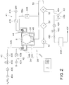
- FIG. 2 is a diagram showing the structure of an etching apparatus incorporated in the substrate liquid treatment system.
- FIG. 3 is a plan view showing substrates held in a processing bath of the etching apparatus.
- FIG. 4 is a graph showing an example of change of silicon concentration in a phosphoric acid solution, during processing of the substrates of one process lot.
- FIG. 5 is a schematic sectional view showing the structure of the substrate to be processed by the etching apparatus.
- FIG. 6 is a schematic sectional view showing the structure of the substrate having been processed by the etching apparatus.
- FIG. 7 is a graph showing another example of change of silicon concentration in a phosphoric acid solution, during processing of substrates of one process lot.
- the substrate liquid treatment system 1 A has a carrier in/out section 2 , a lot forming section 3 , a lot rack section 4 , a lot conveyer section 5 , a lot processing section 6 and a control section 7 .
- the carrier in/out section 2 performs carrying-in/out of a carrier 9 containing a plurality of (e.g., twenty five) substrates (e.g., silicon wafers) 8 which are arrayed in the vertical direction in a horizontal posture.
- a carrier 9 containing a plurality of (e.g., twenty five) substrates (e.g., silicon wafers) 8 which are arrayed in the vertical direction in a horizontal posture.
- the carrier in/out section 2 is provided with a carrier stage 10 configured to allow a plurality of carriers 9 to be placed thereon, a carrier transfer mechanism 11 that transfers a carrier 9 , carrier stocks 12 and 13 each configured to allow a carrier 9 to be temporarily stored thereon, and a carrier stage 14 configured to allow a carrier 9 to be placed thereon.
- the carrier stock 12 temporarily stores the carrier 9 containing the substrates 8 (product substrates), before the substrates 8 are processed in the lot processing section 6 .
- the carrier stock 13 temporarily stores the carrier 9 containing the substrates 8 (product substrates), after the substrates 8 are processed in the lot processing section 6 .
- the carrier in/out section 2 transfers the carrier 9 , which has been carried into the carrier stage 10 from the outside of the substrate liquid treatment system 1 A, to the carrier stock 12 or the carrier stage 14 by using the carrier transfer mechanism 11 .
- the carrier carry-in/out unit 2 transfers the carrier 9 , which is placed on the carrier stage 14 , to the carrier stock 13 or the carrier stage 10 by using the carrier transfer mechanism 11 .
- the carrier 9 which has been transferred to the carrier stage 10 , is transferred to the outside of the substrate liquid treatment system 1 A.
- the lot forming section 3 forms a lot consisting of a plurality of (e.g., fifty) substrates 8 to be simultaneously processed, by combining the substrates 8 accommodated in one or more carrier(s) 9 .
- the lot may be formed such that the patterned surfaces of the substrates 8 are opposed to each other, or such that all the patterned surfaces of the substrates 8 are oriented in the same direction.
- the lot forming section 3 is provided with a substrate transfer mechanism 15 that transfers a plurality of substrates 8 .
- the substrate transfer mechanism 15 can change the posture of the substrates 8 from the horizontal posture to the vertical posture and vice versa.
- the lot forming section 3 transfers the substrates 8 from the carrier 9 placed on the carrier stage 14 to the lot rack section 4 using the substrate transfer mechanism 15 , and places the substrates 8 on the lot rack section 4 to form a lot.
- the lot forming section 3 also transfers a lot placed on the lot rack section 4 to the carrier 9 placed on the carrier stage 14 , by the substrate transfer mechanism 15 .
- the substrate transfer mechanism 15 has two substrate support units each for supporting a plurality of substrates 8 , one being an unprocessed substrate support unit for supporting substrates 8 before being processed (before being transferred by the lot conveyer section 5 ), the other being a processed substrate support unit for supporting substrates 8 after being processed (after being transferred by the lot conveyer section 5 ).
- transferring of particles or the like adhered to the unprocessed substrates 8 to the processed substrates 8 can be prevented.
- a lot which is to be or has been transferred between the lot forming section 3 and the lot processing section 6 by the lot conveyer section 5 , is temporarily placed on lot racks 16 to be on standby.
- the lot rack section 4 is provided with a lot rack 17 for carrying-in provided to allow a lot to be placed thereon before being processed (before being transferred by the lot conveyer section 5 ) and a lot rack 18 for carrying-out provided to allow a lot to be placed thereon after being processed (after being transferred by the lot conveyer section 5 ).
- a lot rack 17 for carrying-in provided to allow a lot to be placed thereon before being processed (before being transferred by the lot conveyer section 5 ) and a lot rack 18 for carrying-out provided to allow a lot to be placed thereon after being processed (after being transferred by the lot conveyer section 5 ).
- a lot rack 17 and 18 On each of the lot racks 17 and 18 , a plurality of substrates 8 of one lot are placed side by side in the back and forth direction in the vertical posture.
- a lot formed in the lot forming section 3 is placed on the lot rack 17 .
- the lot is then transferred to the lot processing section 6 by the lot conveyer section 5 .
- a lot transferred from the lot processing section 6 by the lot conveyer section 5 is placed on the lot rack 18 .
- the lot is then transferred to the lot forming section 3 .
- the lot conveyer section 5 transfers a lot between the lot rack section 4 and the lot processing section 6 , and also transfers a lot within the lot processing section 6 .
- the lot conveyer section 5 is provided with a lot transfer mechanism 19 that transfers a lot.
- the lot transfer mechanism 19 is composed of a rail 20 arranged along the lot rack section 4 and the lot processing section 6 , and a mobile body 21 that moves along the rail 20 while holding a plurality of substrates 8 .
- the mobile body 21 is provided with a substrate holder 22 capable of being moved back and forth.
- the substrate holder 22 is configured to hold a plurality of substrates 8 while they are arrayed side by side in the back and forth direction in the vertical posture.
- the lot conveyer section 5 receives a lot placed on the lot rack 17 by the substrate holder 22 of the lot transfer mechanism 19 , and delivers the lot to the lot processing section 6 .
- the lot conveyer section 5 also receives a lot having been processed in the lot processing section 6 by the substrate holder 22 of the lot transfer mechanism 19 , and transfers the lot to the lot rack 18 . Further, the lot conveyer section 5 transfers the lot within the lot processing section 6 by using the lot transfer mechanism 19 .
- the lot processing section 6 performs a process or a liquid treatment (e.g., an etching process, a cleaning process, a drying process, etc.) to a plurality of substrates 8 forming one lot (process lot), which are arranged side by side in the back and forth direction in the vertical posture.
- a process or a liquid treatment e.g., an etching process, a cleaning process, a drying process, etc.
- a drying apparatus 23 that performs the drying of substrates 8
- a substrate holder cleaning apparatus 24 that performs the cleaning of the substrate holder 22
- a cleaning apparatus 25 that performs the cleaning of substrates 8
- the drying apparatus 23 has a processing bath 27 , and a substrate lifting mechanism 28 provided in the processing bath 27 so as to be vertically movable.
- the processing bath 27 is supplied with a drying gas (e.g., IPA (isopropyl alcohol) or the like).
- IPA isopropyl alcohol
- On the substrate lifting mechanism 28 a plurality of substrates 8 of one lot are held side by side in the back and forth direction in the vertical posture.
- the drying apparatus 23 receives a lot from the substrate holder 22 of the lot transfer mechanism 19 by the substrate lifting mechanism 28 , and moves the lot up and down by the substrate lifting mechanism 28 such that substrates 8 are dried by means of the drying gas supplied to the processing bath 27 . Then, the drying apparatus 23 transfers the lot from the substrate lifting mechanism 28 to the substrate holder 22 of the lot transfer mechanism 19 .
- the substrate holder cleaning apparatus 24 has a processing bath 29 into which a cleaning liquid and a drying gas can be supplied.
- the substrate holder cleaning apparatus 24 cleans the substrate holder 22 , by supplying the cleaning liquid and then supplying the drying gas to the substrate holder 22 of the lot transfer mechanism 19 .
- the cleaning apparatus 25 includes a processing bath 30 for cleaning and a processing bath 31 for rinsing.
- the processing baths 30 and 31 are provided with vertically-movable substrate lifting mechanisms 32 and 33 , respectively.
- a cleaning liquid e.g., SC-1
- a rinsing liquid e.g., pure water
- the etching apparatus 1 includes a processing bath 34 for etching and a processing bath 35 for rinsing.
- the processing baths 34 and 35 are provided with vertically-movable substrate lifting mechanisms 36 and 37 , respectively.
- An etching liquid e.g., phosphoric acid solution
- a rinsing liquid e.g., pure water
- the etching apparatus 1 is the substrate liquid treatment apparatus in one embodiment of the present invention.
- the cleaning apparatus 25 and the etching apparatus 1 have the same structure.
- the description will be made to the etching apparatus (substrate liquid treatment apparatus) 1 .
- the substrate lifting mechanisms 36 holds a plurality of substrates 8 of one lot with the substrates being arrayed side by side to be held in the back and forth direction in the vertical posture.
- the substrate lifting mechanism 36 receives a lot from the substrate holder 22 of the lot transfer mechanism 19 , and the substrate lifting mechanism 36 moves the lot up and down, so that the lot is immersed into the etching liquid in the processing bath 34 thereby to etch the substrates 8 . Thereafter, the etching apparatus 1 delivers the lot from the substrate lifting mechanism 36 to the substrate holder 22 of the lot transfer mechanism 19 .
- the substrate lifting mechanism 37 then receives the lot from the substrate holder 22 of the lot transfer mechanism 19 , and the substrate lifting mechanism 37 moves the lot up and down, so that the lot is immersed in the rinsing liquid in the processing bath 35 thereby to rinse the substrates 8 . Thereafter, the lot is delivered from the substrate lifting mechanism 37 to the substrate holder 22 of the lot transfer mechanism 19 .
- the control section 7 controls operations of the respective sections (the carrier carry-in/out section 2 , the lot forming section 3 , the lot rack section 4 , the lot conveyer section 5 and the lot processing section 6 (notably, the etching apparatus 1 )) of the substrate liquid treatment system 1 A.
- the control section 7 comprises, for example, a computer, and has a computer-readable storage medium 38 .
- the storage medium 38 stores program that controls various processes performed in the substrate liquid treatment apparatus 1 .
- the control section 7 controls the operations of the substrate liquid treatment apparatus 1 by reading out and executing the program stored in the storage medium 38 .
- the program may be one that has been stored in the computer-readable storage medium 38 , or may be one that has been installed to the storage medium 38 of the control section 7 from another storage medium.
- the computer-readable storage medium 38 may be, for example, a hard disc (HD), a flexible disc (FD), a compact disc (CD), a magneto optical disc (MO), or a memory card.
- a liquid process is performed to the substrates 8 by using, as a processing liquid (etching liquid), a solution (phosphoric acid solution) of a chemical (phosphoric acid) having a predetermined concentration.
- the etching apparatus 1 has the aforementioned processing bath 34 that stores, as a processing liquid, a phosphoric acid solution having a predetermined concentration.
- the processing bath 34 has a top-opened inner bath 34 A and a top-opened outer bath 34 B disposed around the upper part of the inner bath 34 A. A phosphoric acid solution overflowing from the inner bath 34 A flows into the outer bath 34 B.
- a circulation line 50 is connected to the bottom of the outer bath 34 B.
- the other end of the circulation line 50 is connected to a processing liquid supplying nozzle 49 disposed in the inner bath 34 A.
- the circulation line 50 is provided with a pump 51 , a heater 52 and a filter 53 in this order from the upstream side. By driving the pump 51 , a circulation flow of the phosphoric acid solution is formed, which flows from the outer bath 34 B through the circulation line 50 and the processing liquid supplying nozzle 49 into the inner bath 34 A, and then flows out therefrom into the outer bath 34 B.
- the processing bath 34 , the circulation line 50 and the devices ( 51 , 52 , 53 and so on) in the circulation line 50 constitute a liquid treatment unit 39 .
- the processing bath 34 and the circulation line 50 constitute a circulation system.
- the processing bath 34 is provided with the aforementioned substrate lifting mechanism 36 .
- the substrate lifting mechanism 36 can hold a plurality of substrates 8 with the substrates 8 being arrayed at horizontal intervals in vertical posture, and can move up and down under that condition.
- the etching apparatus 1 includes a phosphoric acid solution supplying unit 40 that supplies the liquid treatment unit 39 with a phosphoric acid solution, a pure water supplying unit 41 that supplies the liquid treatment unit 39 with pure water, a silicon supplying unit 42 that supplies the liquid treatment unit 39 with a silicon solution, and a phosphoric acid solution draining unit 43 that drains the phosphoric acid solution from the liquid treatment unit 39 .
- the phosphoric acid solution supplying unit 40 supplies a phosphoric acid solution having a predetermined concentration into the circulation system formed of the processing bath 34 and the circulation line 50 (i.e., to any part in the liquid treatment unit 39 ), preferably to the outer bath 34 B as illustrated.
- the phosphoric acid solution supplying unit 40 includes a phosphoric acid solution source 40 A comprising a tank storing a phosphoric acid solution, a phosphoric acid solution supplying line 40 B connecting the phosphoric acid solution source 40 A and the outer bath 34 B, and a flowmeter 40 C, a flow rate regulating valve 40 D and a shutoff valve 40 E that are disposed on the phosphoric acid solution supplying line 40 B in this order from the upstream side.
- the phosphoric acid solution supplying unit 40 can supply, to the outer bath 34 B, a phosphoric acid solution at a controlled flow rate via the flowmeter 40 C and the flow rate regulating valve 40 D.
- the pure water supplying unit 41 supplies pure water in order to replenish water that is lost by evaporation due to the heating of the phosphoric acid solution.
- the pure water supplying unit 41 includes a pure water source 41 A that supplies pure water having a predetermined temperature.
- the pure water source 41 A is connected to the outer bath 34 B through a flow rate regulator 41 B.
- the flow rate regulator 41 B may be composed of a shutoff valve, a flow rate regulating valve, a flowmeter and so on.
- the silicon supplying unit 42 has a silicon source 42 A comprising a tank storing a silicon solution, for example, a liquid in which colloidal silicon is dispersed, and a flow rate regulator 42 B.
- the flow rate regulator 42 B may be composed of a shutoff valve, a flow rate regulating valve, a flowmeter and so on.
- the phosphoric acid solution draining unit 43 is disposed for draining a phosphoric acid solution in the circulation system formed of the liquid treatment unit 39 and the circulation line 50 , i.e., in the liquid treatment unit 39 .
- the phosphoric acid solution draining unit 43 has a draining line 43 A branched from the circulation line 50 , and a flowmeter 43 B, a flow rate regulating valve 43 C, a shutoff valve 43 D and a cooling tank 43 E that are disposed on the draining line 43 A in this order from the upstream side.
- the phosphoric acid solution draining unit 43 can drain a phosphoric acid solution at a controlled flow rate via the flowmeter 43 B and the flow rate regulating valve 43 C.
- the cooling tank 43 E temporarily stores a phosphoric acid solution flowing through the draining line 43 A and cools the same.
- a phosphoric acid solution (see reference numeral 43 F) flowing out from the cooling tank 43 E may be discarded to a factory waste liquid system (not shown), or may be sent to the phosphoric acid solution source 40 A for reuse after removing silicon contained in the phosphoric acid solution by a regeneration apparatus (not shown).
- the draining line 43 A is connected to the circulation line 50 (the filter drain position in the illustration). However, not limited thereto, the draining line 43 A may be connected to another part in the circulation system, e.g., the bottom of the inner bath 34 A.
- the draining line 43 A is provided with a silicon concentration meter 43 G that measures the silicon concentration in the phosphoric acid solution.
- a branch line 55 A is branched from the circulation line 50 to be connected to the outer bath 34 B.
- the branch line 55 A is provided with a phosphoric acid concentration meter 55 B that measures the phosphoric acid concentration in the phosphoric acid solution.
- the outer bath 34 B is provided with a level meter 44 that detects the liquid level in the outer bath 34 B.
- the processing liquid supplying nozzle 49 is formed of a cylindrical body, which extends in the direction in which the substrates 8 are arrayed.
- the processing liquid supplying nozzle 49 discharges, from a plurality of discharge holes formed in its circumferential surface, the processing liquid toward the substrates 8 held by the substrate lifting mechanism 36 .
- the substrate liquid treatment apparatus 1 processes the substrates 8 by controlling operations of the respective sections (the carrier in/out section 2 , the lot forming section 3 , the lot rack section 4 , the lot conveyer section 5 , the lot processing section 6 (the etching apparatus 1 )) by means of the control section 7 in accordance with a process recipe stored in the storage medium 38 .
- the operative components (the shutoff valve, the flow rate regulating valve, the pump, the heater and so on) of the etching apparatus 1 are operated based on operation instruction signals transmitted from the control section 7 .
- the signals indicating detection results are sent from the sensors ( 43 G, 55 B, 44 and so on) to the control section 7 , and the control section 7 uses the detection results for controlling the operative components.
- the phosphoric acid solution supplying unit 40 supplies a phosphoric acid solution to the outer bath 34 B of the liquid treatment unit 39 .
- the pump 51 of the circulation line 50 is activated, so that the aforementioned circulation flow circulating the circulation system is generated.
- the heater 52 of the circulation line 50 is activated such that the phosphoric acid solution in the inner bath 34 A is heated up to a predetermined temperature (e.g., 160° C.). Since the phosphoric acid solution at 160° C. is boiling, water is evaporated therefrom so that a phosphoric acid concentration in the phosphoric acid solution increases as time passes by.
- a predetermined temperature e.g. 160° C.
- pure water is supplied from the pure water supplying unit 41 .
- the supply of pure water for adjusting the phosphoric acid concentration can be performed at any timing when the substrates 8 are being immersed in the processing liquid (i.e., during the liquid treatment of the substrates).
- the supply of pure water for adjusting the phosphoric acid concentration may be performed when the substrates 8 are not being immersed in the processing liquid.
- the silicon concentration in the phosphoric acid solution affects the etch selectivity (etch selection ratio) of the silicon nitride film relative to the silicon oxide film, which are both formed on the substrate 8 .
- the initial silicon concentration is adjusted before the substrates 8 are immersed into the phosphoric acid solution in the inner bath 34 A.
- the adjustment of the initial silicon concentration can be performed by immersing, by the substrate lifting mechanism 36 , a plurality of dummy silicon substrates into the phosphoric acid solution stored in the inner bath 34 A. Such a process is referred to as seasoning. In place of this process, the adjustment of the initial silicon concentration may be performed by supplying a silicon solution to the outer bath 34 B by the silicon supplying unit 42 .
- a preliminary test may be conducted to determine the seasoning condition which enables a desired initial silicon concentration.
- the seasoning may be performed in accordance with the determined condition.
- a preliminary test may be conducted for determining the amount of silicon solution to be supplied, which enables the desired initial silicon concentration.
- the phosphoric acid solution may be supplied to the discharge line 43 A to measure the silicon concentration by the silicon concentration meter 43 G.
- a plurality of substrates 8 e.g., fifty substrates 8 forming one lot (it is also referred to as “process lot” or “batch”), which are held by the substrate lifting mechanism 36 , are immersed into the phosphoric acid solution having a predetermined concentration and a predetermined temperature stored in the inner bath 34 A, so that the substrates 8 are etched (liquid-treated) by the phosphoric acid solution.
- process lot e.g., fifty substrates 8 forming one lot (it is also referred to as “process lot” or “batch”), which are held by the substrate lifting mechanism 36 , are immersed into the phosphoric acid solution having a predetermined concentration and a predetermined temperature stored in the inner bath 34 A, so that the substrates 8 are etched (liquid-treated) by the phosphoric acid solution.
- bubbles generated due to boiling of water elevate in the phosphoric acid solution in the inner bath 34 A, and the phosphoric acid solution circulates in the inner bath 34 A because of the elevating bubbles, whereby the
- the silicon nitride film on the substrate 8 is etched, the silicon derived from the silicon nitride film dissolves in the phosphoric acid solution.
- the silicon concentration in the phosphoric acid solution gradually rises as time passes by.
- Excessively high silicon concentration would result in problems such as deterioration of particle level, clogging of filter and so on.
- a silicon oxide film should be etched to some degree. In such cases, excessively high silicon concentration would result in the situation where the silicon oxide film cannot be etched to the desired degree. In any case, the silicon concentration should be maintained within a range by which a desired process result can be achieved.
- the phosphoric acid solution (which contains relatively a larger amount of silicon) present in the liquid treatment unit (constituted by the processing bath 34 , the circulation line 50 and the devices ( 51 , 52 , 53 , etc.) in the circulation line 50 ), i.e., in the circulation system, is drained at a first drainage flow rate by the phosphoric acid solution draining unit 43 , a phosphoric acid solution free of silicon or a phosphoric acid solution containing only a slight amount of silicon (referred to as “low Si phosphoric acid solution” for simplicity herebelow) is supplied at a first supply flow rate by the phosphoric acid solution supplying unit 40 .
- low Si phosphoric acid solution a phosphoric acid solution free of silicon or a phosphoric acid solution containing only a slight amount of silicon
- the low Si phosphoric acid solution supplied from the phosphoric acid solution supplying unit 40 may be a new (unused) phosphoric acid solution free of silicon, or may be a recycled phosphoric acid solution (which may contain a slight amount of silicon) from which impurities such as silicon are removed after use.
- the total amount of the phosphoric acid solution in the liquid treatment unit 39 in other words, the total amount of the phosphoric acid solution in the circulation system comprising the processing bath 34 and the circulation line 50 is maintained substantially constant.
- the first drainage flow rate and the first supply flow rate are substantially the same.
- the supply flow rate of the phosphoric acid solution supplied from the phosphoric acid solution supplying unit 40 may be decreased by an amount corresponding to an amount of pure water which is being supplied.
- the degree of inhibition of the rise in silicon concentration in the phosphoric acid solution which rise is caused by dissolution of the silicon nitride film, can be changed.
- the silicon concentration rising rate can be reduced.
- the silicon concentration rising rate can be controlled to a negative value.
- the silicon concentration rising rate can be increased.
- the initial silicon concentration is set relatively high and the first drainage flow rate and the first supply flow rate are set relatively high, so that the etching of the substrate 8 of one process lot (meaning a set of, e.g., fifty substrates 8 forming a batch) is performed with the silicon concentration being maintained substantially constant, whereby the etch selectivity (etch selection ratio) is maintained substantially constant.
- the initial silicon concentration is set relatively low and the first drainage flow rate and the first supply flow rate are set relatively low, so that the etching of the substrates 8 of one process lot is performed with the silicon concentration gradually rising with time, whereby the etching selection ratio is gradually increased with time.
- the drainage flow rate and the supply flow rate in the first time period T 1 may be set as the aforementioned first drainage flow rate and the first supply flow rate
- the drainage flow rate and the supply flow rate in the second time period T 2 may be set as a second drainage flow rate and a second supply flow rate that are different from the first drainage flow rate and the first supply flow rate.
- a third time period T 3 may be provided between the first time period T 1 and the second time period T 2 , and the drainage flow rate and the supply flow rate in the third time period T 3 may be set as a third drainage flow rate and a third supply flow rate. According to the above operation, the etch selectivity can be changed depending on the degree of the etching progress.
- the drainage flow rate of the phosphoric acid solution by the phosphoric acid solution draining unit 43 and the supply flow rate of the phosphoric acid solution from the phosphoric acid solution supplying unit 40 in each of the time periods (T 1 , T 2 ) are determined beforehand as constant values (constant values unchanged through one time period) based on the results of a preliminary test. These constant values are stored in the storage medium 38 as target values constituting a part of a process recipe.
- the control section 7 controls the phosphoric acid solution draining unit 43 and the phosphoric acid solution supplying unit 40 such that the drainage flow rate and the supply flow rate correspond to the values specified in the process recipe.
- the silicon concentration in the phosphoric acid solution in the circulation system in each time period can be maintained within a desired range.
- whether the silicon concentration is maintained within an allowable range about the target value can be confirmed (monitored) by using the silicon concentration meter 43 G disposed on the phosphoric acid solution draining unit 43 .
- the silicon solution may be added by the silicon supplying unit 42 to the phosphoric acid solution in the circulation system.
- the substrates 8 are carried out from the processing bath 34 . Then, before substrates 8 of the next lot are put into the processing bath 34 , the phosphoric acid solution is drained from the phosphoric acid solution draining unit 43 and the phosphoric acid solution is supplied from the phosphoric acid solution supplying unit 40 , and silicon solution is supplied from the silicon supplying unit 42 may be supplied in some case, in order to achieve an initial silicon concentration suited for processing of the substrates of the next process lot.
- the substrate 8 having a multi-layered structure there is a process in which silicon nitride layers (SiN) are completely removed so as to completely expose the underlying oxide layers (Oxide).
- silicon nitride layers SiN
- oxide layers Oxide
- the dispersion in etching progress may be caused, for example, by dispersion in film quality of the respective silicon nitride layers, although the dispersion is within an allowable range.
- a safety margin is set in a process time, in statistical consideration of dispersion in time required for etching. That is, the process time is set longer than a time generally required for completely removing all the silicon nitride layers.
- silicon derived from the silicon nitride layer no longer dissolves in the phosphoric acid solution.
- silicon derived from the silicon nitride layer no longer dissolves in the phosphoric acid solution.
- dissolution of silicon rarely occurs.
- the silicon concentration in the phosphoric acid solution in the inner bath 34 A gradually lowers. If the silicon concentration lowers, the etch rate of the silicon oxide layer (SiO 2 ) rises.
- corners of the silicon oxide layer may be etched more than expected.
- the draining of the phosphoric acid solution through the phosphoric acid solution draining unit 43 may be stopped (the drainage flow rate is made zero), and the supply of the phosphoric acid solution from the phosphoric acid solution supplying unit 40 may be stopped (the supply flow rate is made zero).
- the drainage flow rate and the supply flow rate of the phosphoric acid solution in the first time period are set as a first drainage flow rate and a first supply flow rate
- the drainage flow rate and the supply flow rate of the phosphoric acid solution in the second time period are set as a second drainage flow rate and a second supply flow rate (both may be zero in this example) that are smaller than the first drainage flow rate and the first supply flow rate.
- the second drainage flow rate and the second supply flow rate may be larger than the first drainage flow rate and the first supply flow rate.
- a third time period T 3 may be provided between the first time period T 1 and the second time period T 2 , and a third drainage flow rate and a third supply flow rate in the third time period T 3 may be larger than the first drainage flow rate and the first supply flow rate.
- a third time period T 3 may be provided after the second time period T 2 , and a third drainage flow rate and a third supply flow rate in the third time period T 3 may be larger than the first drainage flow rate and the first supply flow rate.
- etching can be performed while achieving optimum etch selectivity in response to the progress of the etching, by changing the silicon concentration of the phosphoric acid solution at least once when the liquid treatment of the substrates 8 of one lot is being performed.
- the drainage flow rate of the phosphoric acid solution by the phosphoric acid solution draining unit 43 and the supply flow rate of the phosphoric acid solution by the phosphoric acid solution supplying unit 40 are controlled such that they correspond to predetermined values.
- a modification is possible.
- the target silicon concentration in each time period may be specified in the process recipe.
- the drainage flow rate of the phosphoric acid solution by the phosphoric acid solution draining unit 43 and the supply flow rate of the phosphoric acid solution by the phosphoric acid solution supplying unit 40 are feedback-controlled based on the detection value of the silicon concentration meter 43 G.
Abstract
Description
Claims (12)
Applications Claiming Priority (2)
| Application Number | Priority Date | Filing Date | Title |
|---|---|---|---|
| JP2016196663A JP6789751B2 (en) | 2016-10-04 | 2016-10-04 | Substrate liquid treatment equipment, substrate liquid treatment method and storage medium |
| JP2016-196663 | 2016-10-04 |
Publications (2)
| Publication Number | Publication Date |
|---|---|
| US20180096855A1 US20180096855A1 (en) | 2018-04-05 |
| US10699910B2 true US10699910B2 (en) | 2020-06-30 |
Family
ID=61758998
Family Applications (1)
| Application Number | Title | Priority Date | Filing Date |
|---|---|---|---|
| US15/723,301 Active US10699910B2 (en) | 2016-10-04 | 2017-10-03 | Substrate liquid treatment apparatus, substrate liquid treatment method and storage medium |
Country Status (4)
| Country | Link |
|---|---|
| US (1) | US10699910B2 (en) |
| JP (1) | JP6789751B2 (en) |
| KR (1) | KR102404963B1 (en) |
| CN (1) | CN107895702B (en) |
Families Citing this family (6)
| Publication number | Priority date | Publication date | Assignee | Title |
|---|---|---|---|---|
| JP6909620B2 (en) * | 2017-04-20 | 2021-07-28 | 株式会社Screenホールディングス | Substrate processing method |
| JPWO2019189133A1 (en) | 2018-03-27 | 2021-03-18 | 日油株式会社 | Sphingomyelin-induced lipids and their production methods |
| JP7224117B2 (en) * | 2018-06-15 | 2023-02-17 | 東京エレクトロン株式会社 | SUBSTRATE PROCESSING APPARATUS AND PROCESSING LIQUID REUSE METHOD |
| JP7101083B2 (en) * | 2018-08-23 | 2022-07-14 | 東京エレクトロン株式会社 | Substrate liquid treatment equipment, substrate liquid treatment method and storage medium |
| JP7158249B2 (en) * | 2018-11-09 | 2022-10-21 | 東京エレクトロン株式会社 | SUBSTRATE PROCESSING METHOD, SUBSTRATE PROCESSING APPARATUS, AND STORAGE MEDIUM |
| CN114540960B (en) * | 2022-04-22 | 2022-07-01 | 江苏英思特半导体科技有限公司 | Circulating tank for silicon wafer corrosion |
Citations (7)
| Publication number | Priority date | Publication date | Assignee | Title |
|---|---|---|---|---|
| JPH09275091A (en) | 1996-04-03 | 1997-10-21 | Mitsubishi Electric Corp | Etching device of semiconductor nitride film |
| JP2000058500A (en) | 1998-08-07 | 2000-02-25 | Matsushita Electron Corp | Etching liquid, production thereof and etching method |
| JP2001023952A (en) | 1999-03-30 | 2001-01-26 | Tokyo Electron Ltd | Etching method and device |
| US20070175387A1 (en) * | 2006-01-30 | 2007-08-02 | Masahiro Kimura | Substrate processing apparatus and substrate processing method |
| US20080305564A1 (en) * | 2007-06-05 | 2008-12-11 | Hisashi Okuchi | Manufacturing apparatus for semiconductor device and manufacturing method for semiconductor device |
| JP2015070080A (en) | 2013-09-27 | 2015-04-13 | 東京エレクトロン株式会社 | Etching method, etching device and storage medium |
| JP2016143684A (en) | 2015-01-30 | 2016-08-08 | 東京エレクトロン株式会社 | Substrate liquid processing apparatus and substrate liquid processing method, and computer readable storage medium stored with substrate liquid processing program |
Family Cites Families (3)
| Publication number | Priority date | Publication date | Assignee | Title |
|---|---|---|---|---|
| JP5368116B2 (en) * | 2008-03-25 | 2013-12-18 | 大日本スクリーン製造株式会社 | Substrate processing apparatus and substrate processing method |
| US9887095B2 (en) * | 2013-03-12 | 2018-02-06 | Taiwan Semiconductor Manufacturing Company, Ltd. | System and method for an etch process with silicon concentration control |
| JP2015195306A (en) * | 2014-03-31 | 2015-11-05 | 芝浦メカトロニクス株式会社 | substrate processing apparatus |
-
2016
- 2016-10-04 JP JP2016196663A patent/JP6789751B2/en active Active
-
2017
- 2017-09-28 CN CN201710899650.8A patent/CN107895702B/en active Active
- 2017-09-29 KR KR1020170128022A patent/KR102404963B1/en active IP Right Grant
- 2017-10-03 US US15/723,301 patent/US10699910B2/en active Active
Patent Citations (12)
| Publication number | Priority date | Publication date | Assignee | Title |
|---|---|---|---|---|
| JPH09275091A (en) | 1996-04-03 | 1997-10-21 | Mitsubishi Electric Corp | Etching device of semiconductor nitride film |
| US6001215A (en) | 1996-04-03 | 1999-12-14 | Mitsubishi Denki Kabushiki Kaisha | Semiconductor nitride film etching system |
| JP2000058500A (en) | 1998-08-07 | 2000-02-25 | Matsushita Electron Corp | Etching liquid, production thereof and etching method |
| JP2001023952A (en) | 1999-03-30 | 2001-01-26 | Tokyo Electron Ltd | Etching method and device |
| US20020001967A1 (en) | 1999-03-30 | 2002-01-03 | Kenji Yokomizo | Etching method and etching apparatus |
| US20020102851A1 (en) | 1999-03-30 | 2002-08-01 | Tokyo Electron Limited | Etching method and etching apparatus |
| US20070175387A1 (en) * | 2006-01-30 | 2007-08-02 | Masahiro Kimura | Substrate processing apparatus and substrate processing method |
| US20080305564A1 (en) * | 2007-06-05 | 2008-12-11 | Hisashi Okuchi | Manufacturing apparatus for semiconductor device and manufacturing method for semiconductor device |
| JP2015070080A (en) | 2013-09-27 | 2015-04-13 | 東京エレクトロン株式会社 | Etching method, etching device and storage medium |
| US20160233106A1 (en) | 2013-09-27 | 2016-08-11 | Tokyo Electron Limited | Etching method, etching apparatus, and storage medium |
| JP2016143684A (en) | 2015-01-30 | 2016-08-08 | 東京エレクトロン株式会社 | Substrate liquid processing apparatus and substrate liquid processing method, and computer readable storage medium stored with substrate liquid processing program |
| US9881799B2 (en) | 2015-01-30 | 2018-01-30 | Tokyo Electron Limited | Substrate liquid processing apparatus, substrate liquid processing method, and computer-readable storage medium |
Non-Patent Citations (1)
| Title |
|---|
| Japanese Office Action (with English translation), Japanese Application No. 2016-196663 dated May 15, 2020 (9 pages). |
Also Published As
| Publication number | Publication date |
|---|---|
| KR20180037598A (en) | 2018-04-12 |
| JP2018060896A (en) | 2018-04-12 |
| CN107895702B (en) | 2023-08-29 |
| US20180096855A1 (en) | 2018-04-05 |
| KR102404963B1 (en) | 2022-06-07 |
| JP6789751B2 (en) | 2020-11-25 |
| CN107895702A (en) | 2018-04-10 |
Similar Documents
| Publication | Publication Date | Title |
|---|---|---|
| US10699910B2 (en) | Substrate liquid treatment apparatus, substrate liquid treatment method and storage medium | |
| US9881799B2 (en) | Substrate liquid processing apparatus, substrate liquid processing method, and computer-readable storage medium | |
| US10985035B2 (en) | Substrate liquid processing apparatus, substrate liquid processing method and computer readable recording medium having substrate liquid processing program recorded therein | |
| JP6999392B2 (en) | Substrate liquid processing equipment | |
| KR102622414B1 (en) | Substrate processing apparatus and substrate processing method | |
| KR102513202B1 (en) | Substrate liquid processing apparatus, substrate liquid processing method, and computer-readable storage medium storing substrate liquid processing program | |
| US11185896B2 (en) | Substrate liquid processing apparatus, substrate liquid processing method, and computer-readable storage medium having substrate liquid processing program stored thereon | |
| US10643874B2 (en) | Substrate liquid processing apparatus, substrate liquid processing method, and storage medium | |
| KR20160134559A (en) | Substrate liquid processing apparatus, substrate liquid processing method, and computer-readable storage medium storing substrate liquid processing program | |
| US11024507B2 (en) | Substrate liquid processing apparatus, substrate liquid processing method, and computer-redable storage medium having substrate liquid processing program stored therein | |
| US10458010B2 (en) | Substrate liquid processing apparatus, substrate liquid processing method, and storage medium | |
| JP2018142695A (en) | Substrate liquid processing apparatus | |
| JP7101075B2 (en) | Substrate liquid processing equipment and storage medium | |
| JP6929729B2 (en) | Substrate liquid treatment method, substrate liquid treatment device and storage medium | |
| JP7198595B2 (en) | SUBSTRATE LIQUID PROCESSING METHOD, SUBSTRATE LIQUID PROCESSING APPARATUS AND STORAGE MEDIUM | |
| KR20200023210A (en) | Substrate liquid processing apparatus, substrate liquid processing method and recording medium | |
| KR102531510B1 (en) | Substrate processing method and substrate processing apparatus | |
| JP6632684B2 (en) | Substrate liquid processing apparatus, substrate liquid processing method, and computer-readable storage medium storing substrate liquid processing program | |
| JP6552687B2 (en) | Substrate liquid processing apparatus, substrate liquid processing method, and computer readable storage medium storing substrate liquid processing program | |
| JP6516908B2 (en) | Etching processing control apparatus using phosphoric acid aqueous solution, etching processing control method using phosphoric acid aqueous solution, and computer readable storage medium storing program for etching substrate with phosphoric acid aqueous solution | |
| JP2018157235A (en) | Substrate liquid processing device, substrate liquid processing method and computer readable storage medium with substrate liquid processing program stored thereon | |
| KR100659842B1 (en) | An apparatus for boat |
Legal Events
| Date | Code | Title | Description |
|---|---|---|---|
| FEPP | Fee payment procedure |
Free format text: ENTITY STATUS SET TO UNDISCOUNTED (ORIGINAL EVENT CODE: BIG.); ENTITY STATUS OF PATENT OWNER: LARGE ENTITY |
|
| AS | Assignment |
Owner name: TOKYO ELECTRON LIMITED, JAPAN Free format text: ASSIGNMENT OF ASSIGNORS INTEREST;ASSIGNOR:SATO, HIDEAKI;REEL/FRAME:044117/0050 Effective date: 20171006 |
|
| STPP | Information on status: patent application and granting procedure in general |
Free format text: RESPONSE TO NON-FINAL OFFICE ACTION ENTERED AND FORWARDED TO EXAMINER |
|
| STPP | Information on status: patent application and granting procedure in general |
Free format text: NON FINAL ACTION MAILED |
|
| STPP | Information on status: patent application and granting procedure in general |
Free format text: RESPONSE TO NON-FINAL OFFICE ACTION ENTERED AND FORWARDED TO EXAMINER |
|
| STPP | Information on status: patent application and granting procedure in general |
Free format text: FINAL REJECTION MAILED |
|
| STPP | Information on status: patent application and granting procedure in general |
Free format text: RESPONSE AFTER FINAL ACTION FORWARDED TO EXAMINER |
|
| STPP | Information on status: patent application and granting procedure in general |
Free format text: NOTICE OF ALLOWANCE MAILED -- APPLICATION RECEIVED IN OFFICE OF PUBLICATIONS |
|
| STPP | Information on status: patent application and granting procedure in general |
Free format text: PUBLICATIONS -- ISSUE FEE PAYMENT VERIFIED |
|
| STCF | Information on status: patent grant |
Free format text: PATENTED CASE |
|
| MAFP | Maintenance fee payment |
Free format text: PAYMENT OF MAINTENANCE FEE, 4TH YEAR, LARGE ENTITY (ORIGINAL EVENT CODE: M1551); ENTITY STATUS OF PATENT OWNER: LARGE ENTITY Year of fee payment: 4 |