US10690601B2 - Method and device for compensating for a material web offset in material web inspection - Google Patents
Method and device for compensating for a material web offset in material web inspection Download PDFInfo
- Publication number
- US10690601B2 US10690601B2 US15/789,232 US201715789232A US10690601B2 US 10690601 B2 US10690601 B2 US 10690601B2 US 201715789232 A US201715789232 A US 201715789232A US 10690601 B2 US10690601 B2 US 10690601B2
- Authority
- US
- United States
- Prior art keywords
- material web
- pictures
- picture
- lighting
- active partial
- Prior art date
- Legal status (The legal status is an assumption and is not a legal conclusion. Google has not performed a legal analysis and makes no representation as to the accuracy of the status listed.)
- Active, expires
Links
Images


Classifications
-
- G—PHYSICS
- G01—MEASURING; TESTING
- G01N—INVESTIGATING OR ANALYSING MATERIALS BY DETERMINING THEIR CHEMICAL OR PHYSICAL PROPERTIES
- G01N21/00—Investigating or analysing materials by the use of optical means, i.e. using sub-millimetre waves, infrared, visible or ultraviolet light
- G01N21/84—Systems specially adapted for particular applications
- G01N21/88—Investigating the presence of flaws or contamination
- G01N21/89—Investigating the presence of flaws or contamination in moving material, e.g. running paper or textiles
-
- G—PHYSICS
- G01—MEASURING; TESTING
- G01N—INVESTIGATING OR ANALYSING MATERIALS BY DETERMINING THEIR CHEMICAL OR PHYSICAL PROPERTIES
- G01N21/00—Investigating or analysing materials by the use of optical means, i.e. using sub-millimetre waves, infrared, visible or ultraviolet light
- G01N21/84—Systems specially adapted for particular applications
- G01N21/88—Investigating the presence of flaws or contamination
- G01N21/8851—Scan or image signal processing specially adapted therefor, e.g. for scan signal adjustment, for detecting different kinds of defects, for compensating for structures, markings, edges
-
- B—PERFORMING OPERATIONS; TRANSPORTING
- B41—PRINTING; LINING MACHINES; TYPEWRITERS; STAMPS
- B41F—PRINTING MACHINES OR PRESSES
- B41F33/00—Indicating, counting, warning, control or safety devices
- B41F33/0036—Devices for scanning or checking the printed matter for quality control
-
- B—PERFORMING OPERATIONS; TRANSPORTING
- B65—CONVEYING; PACKING; STORING; HANDLING THIN OR FILAMENTARY MATERIAL
- B65H—HANDLING THIN OR FILAMENTARY MATERIAL, e.g. SHEETS, WEBS, CABLES
- B65H23/00—Registering, tensioning, smoothing or guiding webs
- B65H23/04—Registering, tensioning, smoothing or guiding webs longitudinally
- B65H23/18—Registering, tensioning, smoothing or guiding webs longitudinally by controlling or regulating the web-advancing mechanism, e.g. mechanism acting on the running web
- B65H23/188—Registering, tensioning, smoothing or guiding webs longitudinally by controlling or regulating the web-advancing mechanism, e.g. mechanism acting on the running web in connection with running-web
- B65H23/192—Registering, tensioning, smoothing or guiding webs longitudinally by controlling or regulating the web-advancing mechanism, e.g. mechanism acting on the running web in connection with running-web motor-controlled
-
- G—PHYSICS
- G01—MEASURING; TESTING
- G01M—TESTING STATIC OR DYNAMIC BALANCE OF MACHINES OR STRUCTURES; TESTING OF STRUCTURES OR APPARATUS, NOT OTHERWISE PROVIDED FOR
- G01M11/00—Testing of optical apparatus; Testing structures by optical methods not otherwise provided for
-
- G—PHYSICS
- G01—MEASURING; TESTING
- G01N—INVESTIGATING OR ANALYSING MATERIALS BY DETERMINING THEIR CHEMICAL OR PHYSICAL PROPERTIES
- G01N21/00—Investigating or analysing materials by the use of optical means, i.e. using sub-millimetre waves, infrared, visible or ultraviolet light
- G01N21/84—Systems specially adapted for particular applications
- G01N21/88—Investigating the presence of flaws or contamination
- G01N21/8806—Specially adapted optical and illumination features
-
- G—PHYSICS
- G01—MEASURING; TESTING
- G01N—INVESTIGATING OR ANALYSING MATERIALS BY DETERMINING THEIR CHEMICAL OR PHYSICAL PROPERTIES
- G01N21/00—Investigating or analysing materials by the use of optical means, i.e. using sub-millimetre waves, infrared, visible or ultraviolet light
- G01N21/84—Systems specially adapted for particular applications
- G01N21/88—Investigating the presence of flaws or contamination
- G01N21/89—Investigating the presence of flaws or contamination in moving material, e.g. running paper or textiles
- G01N21/8901—Optical details; Scanning details
- G01N21/8903—Optical details; Scanning details using a multiple detector array
-
- G—PHYSICS
- G06—COMPUTING OR CALCULATING; COUNTING
- G06T—IMAGE DATA PROCESSING OR GENERATION, IN GENERAL
- G06T7/00—Image analysis
- G06T7/0002—Inspection of images, e.g. flaw detection
- G06T7/0004—Industrial image inspection
-
- H—ELECTRICITY
- H04—ELECTRIC COMMUNICATION TECHNIQUE
- H04N—PICTORIAL COMMUNICATION, e.g. TELEVISION
- H04N23/00—Cameras or camera modules comprising electronic image sensors; Control thereof
- H04N23/56—Cameras or camera modules comprising electronic image sensors; Control thereof provided with illuminating means
-
- H—ELECTRICITY
- H04—ELECTRIC COMMUNICATION TECHNIQUE
- H04N—PICTORIAL COMMUNICATION, e.g. TELEVISION
- H04N23/00—Cameras or camera modules comprising electronic image sensors; Control thereof
- H04N23/90—Arrangement of cameras or camera modules, e.g. multiple cameras in TV studios or sports stadiums
-
- H—ELECTRICITY
- H04—ELECTRIC COMMUNICATION TECHNIQUE
- H04N—PICTORIAL COMMUNICATION, e.g. TELEVISION
- H04N25/00—Circuitry of solid-state image sensors [SSIS]; Control thereof
- H04N25/40—Extracting pixel data from image sensors by controlling scanning circuits, e.g. by modifying the number of pixels sampled or to be sampled
- H04N25/46—Extracting pixel data from image sensors by controlling scanning circuits, e.g. by modifying the number of pixels sampled or to be sampled by combining or binning pixels
-
- H04N5/2256—
-
- H04N5/247—
-
- H04N5/347—
-
- G—PHYSICS
- G01—MEASURING; TESTING
- G01N—INVESTIGATING OR ANALYSING MATERIALS BY DETERMINING THEIR CHEMICAL OR PHYSICAL PROPERTIES
- G01N21/00—Investigating or analysing materials by the use of optical means, i.e. using sub-millimetre waves, infrared, visible or ultraviolet light
- G01N21/84—Systems specially adapted for particular applications
- G01N21/88—Investigating the presence of flaws or contamination
- G01N21/8851—Scan or image signal processing specially adapted therefor, e.g. for scan signal adjustment, for detecting different kinds of defects, for compensating for structures, markings, edges
- G01N2021/8854—Grading and classifying of flaws
- G01N2021/8867—Grading and classifying of flaws using sequentially two or more inspection runs, e.g. coarse and fine, or detecting then analysing
-
- G—PHYSICS
- G01—MEASURING; TESTING
- G01N—INVESTIGATING OR ANALYSING MATERIALS BY DETERMINING THEIR CHEMICAL OR PHYSICAL PROPERTIES
- G01N21/00—Investigating or analysing materials by the use of optical means, i.e. using sub-millimetre waves, infrared, visible or ultraviolet light
- G01N21/84—Systems specially adapted for particular applications
- G01N21/88—Investigating the presence of flaws or contamination
- G01N21/8851—Scan or image signal processing specially adapted therefor, e.g. for scan signal adjustment, for detecting different kinds of defects, for compensating for structures, markings, edges
- G01N2021/8887—Scan or image signal processing specially adapted therefor, e.g. for scan signal adjustment, for detecting different kinds of defects, for compensating for structures, markings, edges based on image processing techniques
-
- G—PHYSICS
- G06—COMPUTING OR CALCULATING; COUNTING
- G06T—IMAGE DATA PROCESSING OR GENERATION, IN GENERAL
- G06T2207/00—Indexing scheme for image analysis or image enhancement
- G06T2207/30—Subject of image; Context of image processing
- G06T2207/30108—Industrial image inspection
- G06T2207/30124—Fabrics; Textile; Paper
Definitions
- the present invention relates to a method and a device for compensating for a material web offset in monitoring and inspection systems for machines with continually transported products, such as material webs.
- the material webs are passed through monitoring or inspection systems that take pictures of the material webs. These pictures can be checked by an operator or automatically. In order to guarantee that pictures are of a high quality, the material webs may be lit for the pictures using corresponding devices.
- an attempt is made to capture the entire material web (100% inspection) with two types of lighting.
- more than two, in other words three, four or five types of lighting may also be used.
- the conditional alternating or staggered taking of pictures with different types of lighting and picture parameters means, for example, that two sequences of pictures with different information can be assessed.
- an offset is produced here between the taking of individual pictures and the sequences of pictures in the direction of movement of the material web which, for example, have been taken with incident lighting and transmitted light lighting. The effects of the offset may be greater the faster the web speed, the higher the resolution of the matrix chip and the greater the delay between the taking of pictures and sequences of pictures.
- the aim of the present invention is therefore to provide a device and a method which overcome the disadvantages of software compensation.
- the present invention relates to a method for compensating for a material web offset in inspection systems for material webs according to claim 1 and to a device for monitoring and/or inspecting material webs according to claim 9 .
- the method according to the invention for compensating for a material web offset in inspection systems for material webs which are moving in the direction of a material web length and/or a material web width comprises the following steps: taking a first picture of a first portion of a material web at a first point in time with a camera which comprises a matrix chip; and taking a second picture of a second portion of the material web at a second point in time with the camera, wherein a first active partial surface of the matrix chip is used for the first picture and a second active partial surface of the matrix chip is used for the second picture, and wherein the first active partial surface and the second active partial surface are not identical.
- the dynamic adjustment of the active partial surface used by the matrix chip allows a direct and exact synchronization of two sequences of pictures of a material web and is independent of the characteristics of the material web (which are required, for example, when compensating for the offset using software).
- two (or more) sequences of pictures taken at very slightly different times can be directly captured and laid exactly on top of one another. There is therefore no need for any complex and sometimes completely impossible or at least unsatisfactory compensating for any offset in the direction of the material web length in the pictures using software evaluation.
- the image capture frequency can also be increased by reducing the size of the active surface of the matrix chip. This is particularly advantageous when carrying out the multi-inspection of moving objects (that is to say when inspecting them with different types of lighting).
- a size and/or a position of the first and second active partial surfaces of the matrix chip and thereby the field of vision of the camera in the direction of the material web length and/or in the direction of the material web width may be dynamically adjusted.
- the first portion and the second portion may be two identical material web portions.
- the first portion and the second portion may be two different material web portions.
- the second active partial surface may be offset compared to the first active partial surface by a prescribed offset in the direction of the material web length and/or in the direction of the material web width.
- This is advantageous because both an offset of the material web in the direction of the material web length and an offset of the material web in the direction of the material web width can therefore be compensated for using the hardware.
- This is of particular advantage if, for example, the edges of the material web cannot be captured for an offset in the direction of the material web width (with respect to possible software compensation) or the field of vision is adjusted to the use of the material web width.
- the first picture may be part of a first sequence of pictures of the material web and the second picture may be part of a second sequence of pictures of the material web.
- a first sequence may be created with a plurality of first pictures in order to produce the first sequence of pictures of the material web and a second sequence may be created with a plurality of second pictures in order to produce the second sequence of pictures of the material web. All of the pictures in the first sequence of pictures may be taken with the first active partial surface of the matrix chip and all of the pictures in the second sequence of pictures may be taken with the second active partial surface of the matrix chip here or the second active partial surface of the matrix chip may in each case be adjusted for the pictures in the second sequence of pictures.
- the material web may be lit with a first type of lighting for the first and second pictures.
- the material web may be lit with a first type of lighting for the first picture and the material web may be lit with a second type of lighting for the second picture.
- a first picture may respectively be taken with the first type of lighting and a second picture may respectively be taken with the second type of lighting, these pictures being taken of a plurality of portions of the material web following one another in the direction of the material web length, wherein the first pictures together produce a first sequence of pictures of the material web and the second pictures produce a second sequence of pictures of the material web.
- At least one of the first and second sequences of pictures may be used for web monitoring and/or inspection.
- the first and/or the second sequences of pictures may be visually displayed for a user.
- the material web may be lit in the entire field of vision of the camera for the first and/or the second picture.
- the material web may in each case be selectively lit according to the first and second active partial surfaces of the matrix chip.
- the material web may be lit in traversing fashion with respect to the direction of the material web width. Further pictures of corresponding further portions may also be taken at corresponding further points in time using corresponding further active partial surfaces of the matrix chip, wherein the further portions are identical to the first portion and/or the second portion. Further types of lighting may be used to light the material web for the further pictures.
- the types of lighting may, for example, be selected from among incident lighting, background lighting and transmitted light lighting.
- a field of vision of the camera may be designed to cover at least the entire width of the material web.
- the field of vision of the camera in the direction of the material web width may be greater than the material web width.
- the first and second active partial surfaces may be adjusted on the basis of a signal from a material web position sensor, in particular a size and/or a position of the first and second active partial surfaces in the direction of the material web width.
- the second point in time may be offset by 0.0001 to 0.01 seconds, in particular by 0.0005 to 0.001 seconds with respect to the first point in time.
- the material web may be moved at a web speed of at least 150 m/min, in particular at least 500 m/min, and preferably at least 900 m/min in the direction of the material web length.
- a sensor may also be provided to determine the distance travelled by or the speed of the material web in the direction of the material web length.
- a distance travelled by the material web in the direction of the material web length may be measured and the first point in time for the first picture and/or the second point in time for the second picture may thereby be calculated and provided to the camera.
- a speed of the material web may be measured and a time lag between the first picture and the second picture can thereby be controlled.
- a plurality of cameras may be provided with a matrix chip, wherein the cameras are arranged distributed over the material web width so that the fields of vision of the cameras in the direction of the material web width adjoin one another or overlap, wherein the plurality of cameras take corresponding first and second pictures and the first and second pictures are combined to form two coherent sequences of pictures.
- the field of vision of the camera may be arranged in traversing fashion with respect to the direction of the material web width.
- the plurality of cameras may be arranged in traversing fashion with respect to the direction of the material web width.
- At least one camera may be provided on a front side of the material web and at least one camera may be provided on a rear side of the material web and first and second pictures may be taken of the front side and the rear side of the material web.
- the invention also comprises a device for monitoring and/or inspecting material webs which are moving in the direction of a material web length and/or a material web width.
- the device comprises a camera which has a matrix chip, wherein partial surfaces of the matrix chip may be activated independently of one another, and a control unit.
- the control unit is designed to have a first partial surface of the matrix chip activated in order to take a first picture of a first portion of the material web at a first point in time; and to have a second partial surface of the matrix chip activated in order to take a second picture of a second portion of the material web at a second point in time, wherein the first active partial surface and the second active partial surface are not identical.
- a size and/or a position of the first and second active partial surfaces of the matrix chip and thereby the field of vision of the camera in the direction of the material web length and/or in the direction of the material web width may be dynamically adjusted.
- the first portion and the second portion may be two identical material web portions.
- the first portion and the second portion may be two different material web portions.
- control unit may be designed to select the first and second active partial surfaces so that the second active partial surface is offset compared to the first active partial surface by a prescribed offset in the direction of the material web length and/or in the direction of the material web width.
- the first picture may be part of a first sequence of pictures of the material web and the second picture may be part of a second sequence of pictures of the material web.
- the control unit may be designed to have a first sequence created with a plurality of first pictures in order to produce the first sequence of pictures of the material web and to have a second sequence created with a plurality of second pictures in order to produce the second sequence of pictures of the material web.
- the control unit may be designed to have all of the pictures in the first sequence of pictures taken with the first active partial surface of the matrix chip and all of the pictures in the second sequence of pictures taken with the second active partial surface of the matrix chip here or to have the second active partial surface of the matrix chip in each case adjusted for the pictures in the second sequence of pictures.
- the device may have a first lighting device so that the material web may be lit with a first type of lighting for the first and second pictures.
- the device may have first and second lighting devices so that a first type of lighting may be used for the first picture of the material web and a second type of lighting may be used for the second picture of the material web.
- the control unit may be designed to have a first picture respectively taken with the first type of lighting and a second picture respectively taken with the second type of lighting, these pictures being taken of a plurality of portions of the material web following one another in the direction of the material web length, wherein the first pictures together produce a first sequence of pictures of the material web and the second pictures produce a second sequence of pictures of the material web.
- the control unit may be designed to have the material web lit in the entire field of vision of the camera for the first and/or the second picture, or to have the material web in each case selectively lit according to the first and second active partial surfaces of the matrix chip.
- the first and/or the second lighting devices may be arranged in traversing fashion in relation to the direction of the material web width.
- the control unit may be designed to have further partial surfaces of the matrix chip activated in order to take further pictures of corresponding further portions at corresponding further points in time, wherein the further portions are identical to the first portion and/or the second portion.
- the device may comprise further lighting devices so that the material web may be lit with further types of lighting for the further pictures.
- the lighting devices may be designed to provide at least one type of lighting selected from among incident lighting, background lighting and transmitted light lighting.
- the camera may have a field of vision to cover at least the entire width of the material web.
- the field of vision of the camera in the direction of the material web width may be greater than the material web width.
- the device may also have a material web position sensor and the control unit may also be designed to have the first and second active partial surfaces adjusted on the basis of a signal from a material web position sensor, in particular to have a size and/or a position of the first and second active partial surfaces in the direction of the material web width adjusted.
- control unit may be designed to have the second point in time offset by 0.0001 to 0.01 seconds, in particular by 0.0005 to 0.001 seconds with respect to the first point in time.
- a sensor may also be provided to determine the distance travelled by or the speed of the material web in the direction of the material web length.
- the device may be designed to measure a distance travelled by the material web in the direction of the material web length and thereby to calculate the first point in time for the first picture and/or the second point in time for the second picture and provide it to the camera.
- the device may be designed to measure the speed of the material web and thereby to control a time lag between the first picture and the second picture.
- a plurality of cameras may be provided with a matrix chip, wherein the cameras are arranged distributed over the material web width so that the fields of vision of the plurality of cameras in the direction of the material web width adjoin one another or overlap.
- the control unit may be designed to have the plurality of cameras take corresponding first and second pictures and to have the first and second pictures combined to form two coherent sequences of pictures.
- the field of vision of the camera may be arranged in traversing fashion with respect to the direction of the material web width and/or, if a plurality of cameras are provided, the plurality of cameras may be arranged in traversing fashion with respect to the direction of the material web width.
- At least one camera may be provided on a front side of the material web and at least one camera may be provided on a rear side of the material web, wherein the control unit may be designed to have first and second pictures respectively taken of the front side and the rear side of the material web.
- the device may also comprise a lens with a fixed focal length.
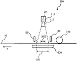
- FIG. 1 shows a schematic representation of a device according to the invention for material web monitoring or material web inspection according to an exemplary embodiment
- FIG. 2 shows two views of a material web with sequences of pictures laid on top
- FIG. 3 shows two schematic representations of a matrix chip with correspondingly activated partial surfaces
- FIG. 4 shows two further schematic representations of a matrix chip with correspondingly activated partial surfaces.
- material web used below is to be interpreted broadly and relates to all types of products which are automatically transported during processing and for which monitoring or inspection is required. This includes, amongst other things, printed paper products, materials and fabrics, packaging and raw materials for packaging, labels, etc.
- the material webs do not have to be in infinitely continuous form here, but may also be in the form of successive sheets.
- the device according to the invention and the method according to the invention may be used for monitoring and/or inspecting all of these products.
- FIG. 1 is a schematic depiction of a side view of a device 100 for monitoring and/or inspecting a material web 10 .
- the device 100 may be used for all of the methods for compensating for a material web offset described below. In addition to monitoring the web/inspection, the device may also be used to measure color density or spectral color.
- the device 100 comprises a camera 110 which has a matrix chip 20 , for example a CCD or CMOS sensor.
- the camera 110 may be suitable for 1D, 2D and/or 3D pictures and may be a color or a black-and-white camera.
- the camera 110 or the field of vision of the camera 110 may be arranged either in parallel or in traversing fashion with respect to the direction of the material web width x (see FIG. 2 ).
- FIG. 1 also shows different devices for lighting the material web 10 .
- one or two lighting devices 130 are provided above the material web 10 and one lighting device 150 is provided below the material web 10 .
- Alternative embodiments may also have only one lighting device or more than two lighting devices.
- FIG. 1 also shows a lens 112 for the camera 110 which preferably has a fixed focal length (fixed-focus lens). In alternative configurations, a zoom lens may also be used.
- a sensor 140 is also provided which measures the distance travelled by or the speed of the material web. Encoders, proximity switches, print mark sensors and direct speed sensors, for example, may be used as sensors here. Use may be made, for example, of rotary encoders (incremental rotary encoders or rotary pulse encoders) which are usually used with a wheel. The wheel, having a known rolling circumference, sits on the material web and, for example, generates several pulses per rotation. The distance travelled by the material web in the direction of the material web length y can be determined by the number of pulses counted.
- the material web speed can then be determined, for example, by reference to the number of pulses counted per unit of time and by reference to the distance travelled, that is to say it can be calculated by reference to the time and distance values (see example hereof below).
- the material web 10 is preferably moved in the direction of a material web length y, but can also be moved in the direction of a material web width x (see FIG. 2 ).
- the material web 10 may, for example, be moved at a web speed of at least 150 m/min, in particular at least 500 m/min, and preferably at least 900 m/min in the direction of the material web length y.
- the device 100 also comprises a control unit (not shown in FIG. 1 ) which controls all of the activities of the device and processes corresponding signals, for example from the sensor 140 or other external sensors.
- a control unit (not shown in FIG. 1 ) which controls all of the activities of the device and processes corresponding signals, for example from the sensor 140 or other external sensors.
- one or more monitors may be provided to visually display the pictures taken by the camera or the picture sequences created (not shown in FIG. 1 ).
- the method according to the invention enables a material web offset which arises in respect of two successive pictures to be compensated for without any complicated software.
- This is made possible by adopting the following approach: taking a first picture of a first portion of the material web 10 at a first point in time with the camera 110 which comprises the matrix chip 20 , and then taking a second picture of a second portion of the material web 10 at a second point in time with the camera 110 .
- the particular feature here is that, as shown in FIG. 3 and FIG. 4 , a first active partial surface 22 of the matrix chip 20 is used for the first picture and a second active partial surface 24 of the matrix chip 20 is used for the second picture, wherein the first active partial surface and the second active partial surface are not identical.
- the second point in time may be offset, for example, by 0.0001 to 0.01 seconds, in particular by 0.0005 to 0.001 seconds with respect to the first point in time.
- An active surface of the matrix chip 20 is understood to be a partial surface of the matrix chip 20 which is activated for taking a picture.
- the principle of a “Region of Interest” (ROI, see FIG. 1 ) is applied here, wherein the actually active surface, that is to say the resolution, of a matrix chip 20 (as already mentioned, CMOS chips, CCD chips or chips with an FPGA, for example, may be used here) is adjusted. This means that it is not the entire surface of the chip and therefore not the maximum field of vision (the maximum field of vision 150 of the camera in the direction of the material web length y is indicated in FIG.
- this is a fictitious example to illustrate the principle of the invention because the matrix chips actually used have a much larger number of pixels (more than 100 megapixels).
- second active partial surface 24 For a second picture, use may be made of a second active partial surface 24 which is shifted by a pixel width (of the notional pixels in the illustration in FIG. 3 ) in the direction of the material web length y.
- the second picture may be shifted by more than one pixel.
- first and second sequences of pictures may then be created by continuously taking first and second pictures with the corresponding partial surfaces 22 , 24 and combining them to form sequences of pictures (of which more below).
- the device and the method have numerous advantages.
- the dynamic adjustment of the active partial surfaces 22 , 24 used by the matrix chip 20 allows a direct and exact synchronization of two sequences of pictures of a material web 10 and is independent of the characteristics of the material web 10 (which are required, for example, when compensating for the offset using software).
- two (or more) sequences of pictures taken at very slightly different times can be directly captured and laid exactly on top of one another. There is therefore no need for any complex and sometimes completely impossible or at least unsatisfactory compensating for any offset in the Y direction (see ⁇ y in FIG. 2 ) in the pictures using software evaluation.
- FIG. 2 To illustrate the offset in the direction of the material web length y when the material web 10 moves in this direction, two material webs 10 are shown in FIG. 2 , in which web portions have respectively been captured at very slightly different points in time and these may be combined to form sequences of pictures 30 a , 30 b . Although, in total, these sequences of pictures respectively cover the entire material web 10 (full inspection), they are offset in the direction of movement of the material web (in this case in direction y) by ⁇ y because the material web 10 has always moved a little further between two successive pictures as a function of the material web speed and the delay of the camera 110 .
- the following offset ⁇ y may, for example, arise under the following framework parameters:
- Such offsets may be dynamically compensated for directly using the device 100 according to the invention and the method according to the invention by activating corresponding partial surfaces 22 , 24 of the matrix chip 20 so that identical portions may be captured in two successive pictures.
- a further advantage of the invention is that the image capture frequency may be increased by reducing the size of the active surfaces 22 , 24 of the matrix chip 20 . This is particularly advantageous when carrying out the multi-inspection of moving objects (that is to say when inspecting them with different types of lighting). Using the method according to the invention and the device 100 according to the invention, it is therefore possible to ensure optimal referencing (hardware compensation) of several sequences of pictures. This consequently also allows a material web to be fully inspected accurately using multi-inspection systems with different types of lighting and without using additional software compensation for referencing. This also leads to a potential saving in the required computer power.
- a size and/or a position of the first and second active partial surfaces 22 , 24 of the matrix chip 20 and thereby the field of vision of the camera 110 in the direction of the material web length y and/or in the direction of the material web width x may be dynamically adjusted.
- Factors which also influence the adjustment of the active partial surfaces are, for example, the current web speed (for example measured by the sensor 140 ), the current camera resolution and the current delay between taking two pictures, wherein the delay may either be fixed in advance or may be dynamically adjusted (see in relation hereto the example below).
- the device may be used for different applications.
- the first portion and the second portion may be two identical material web portions. This means that the same portion of the material web 10 is pictured twice in order, for example, to be able to use two different types of lighting in multi-inspection. Use may also be made of more than two types of lighting and a corresponding number of pictures may be taken.
- the first portion and the second portion may be two different material web portions. Two different portions of the material web are then pictured, but also with different active partial surfaces 22 , 24 in order, for example, to be able to compensate for a sudden deviation in a condition relating to the offset of the material web 10 in the direction of the material web length y or of the material web width x.
- This may, for example, be used in devices with just one type of lighting.
- Such an event may, for example, be a sudden increase in the material web speed (and therefore a kind of offset such as offset ⁇ y of the material web 10 in the direction of the material web length y in FIG. 2 ) or a slipping of the material web transversely to the direction of movement (offset of the material web 10 in the direction of the material web width x).
- the second active partial surface 24 may be offset compared to the first active partial surface 22 by a prescribed offset in the direction of the material web length y and/or in the direction of the material web width x.
- This is advantageous because it is therefore possible to compensate for both an offset ⁇ y of the material web 10 in the y direction and also then an offset of the material web 10 in the x direction using the hardware.
- This is of particular advantage if, for example, the edges of the material web cannot be captured for an offset in the x direction (with respect to possible software compensation) or the field of vision of the camera 110 is adjusted to the actual use of the material web 10 .
- the first picture may be part of a first sequence of pictures of the material web 10 and the second picture may be part of a second sequence of pictures of the material web 10 .
- the first sequence of pictures of the material web 10 is created from a plurality of first pictures and the second sequence of pictures is created from a plurality of second pictures here. Provision may be made for all of the pictures in the first sequence of pictures to be taken with the first active partial surface 22 of the matrix chip 20 and all of the pictures in the second sequence of pictures to be taken with the second active partial surface 24 of the matrix chip 20 . It is also possible for the second active partial surfaces 24 of the matrix chip to be adjusted in each case for the pictures in the second sequence of pictures. Factors such as the current web speed, the current camera resolution and the current delay between taking two pictures may be taken into account here.
- the device has different lighting devices.
- the material web 10 may be lit with the same first type of lighting (for example with lighting device 130 ) for the first and second pictures.
- the material web 10 may be lit with a first type of lighting (for example with lighting device 130 ) for the first picture and the material web 10 may be lit with a second type of lighting (for example with lighting device 120 ) for the second picture.
- a first picture may respectively be taken with the first type of lighting and a second picture may respectively be taken with the second type of lighting, these pictures being taken of a plurality of portions of the material web 10 following one another in the direction of the material web length y, wherein the first pictures together produce the first sequence of pictures of the material web 10 and the second pictures produce the second sequence of pictures of the material web 10 .
- the sequences of pictures generated in this way may then, for example, be visually displayed for a user on one or more monitors.
- web monitoring may also be carried out simultaneously by a user. Alternatively, however, web monitoring may also be carried out using a separate sequence of pictures.
- the material web 10 may be lit in the entire field of vision 150 of the camera 110 for the first and/or the second picture or alternatively in each case selectively lit according to the first and second active partial surfaces 22 , 24 of the matrix chip. It is also possible for the material web 10 to be lit in traversing fashion with respect to the direction of the material web width x.
- the device may also be used for multi-inspection with three or more sequences of pictures.
- further pictures of corresponding further portions are then taken at corresponding further points in time using corresponding further active partial surfaces of the matrix chip 20 , wherein the further portions are identical to the first portion and/or the second portion.
- Further types of lighting may be used to light the material web 10 for these further pictures.
- Further lighting devices may of course be provided in addition to the lighting devices 120 , 130 shown. The types of lighting may, for example, be selected from among incident lighting, background lighting and transmitted light lighting.
- a series of lighting properties may be provided here: homogeneous or inhomogeneous lighting, direct, diffuse, focused or collimated lighting, coaxial, transmissive and/or polarized lighting, different lighting angles and light field or dark field lighting, light wavelengths in the UV, visible or IR range (in order, for example, to be able to inspect security features too), single-colored (monochrome), multicolored (polychrome) or color matchable or controllable (RGB) lighting, surface lighting or line lighting, and constant or flash lighting. In the case of incident lighting and transmitted light lighting, these may be used alternately or at the same time.
- the lighting devices may be configured as a tunnel lighting system, a tube lighting system or a dome lighting system, and may be adjusted modularly or to the material web width.
- Light bulbs, glow-discharge lamps, LED lighting, OLED lighting or laser lighting may be used as means of lighting.
- the respective types of lighting and properties may be used, for example, for the following multi-inspection: Printed image inspection with visible incident light, label inspection with visible transmitted light and inspection of UV security features with UV incident light.
- the field of vision of the camera 110 may be designed to cover at least the entire width of the material web. As already described above, the field of vision of the camera 110 in the direction of the material web width x may, in particular, be greater than the material web width.
- the first and second active partial surfaces 22 , 24 may be adjusted on the basis of a signal from the material web position sensor (not shown in FIG. 1 ), in particular a size and/or a position of the first and second active partial surfaces 22 , 24 in the direction of the material web width x. In addition to the position of the material web 10 , the following factors may in turn also influence the adjustment of the active partial surfaces 22 , 24 : the current web speed, the current camera resolution and the current delay between taking two pictures.
- the delay that is to say the time lag between the first and the second picture, may either be fixed in advance or adjusted according to the material web movement.
- the delay here is a function of a first trigger which triggers the first picture (at the first point in time) and a second trigger which triggers the second picture (at a second point in time).
- the material web offset ⁇ y is produced because of the delay between the first trigger and the second trigger (see FIG. 2 ).
- a time lag between these two triggers (that is to say the two pictures) may be fixed in advance and has a lower limit, for example, based on the maximum image capture frequency of the camera 110 .
- the first and second points in time for the two triggers may also be dynamically adjusted.
- the abovementioned sensor 140 may be used here to measure the distance travelled by or the speed of the material web 10 . This is to be described below by reference to a simple numerical example for a sensor with a wheel.
- the second picture is therefore taken with an offset of ⁇ y 132 mm. Since the 132 mm offset of ⁇ y corresponds to 600 pixels in the matrix chip example, the ROI for the second picture therefore has to be offset by 600 pixels in the direction of the material web length y in order to capture the same material web portion (with different lighting).
- the correction value for the ROI may therefore be determined by the number of pulses.
- the first point in time for the first trigger or the first picture and the second point in time for the second trigger or the second picture may therefore be determined by the distance travelled by the wheel and the pulses of the encoder. For example, the first picture may be taken after a first number of pulses and the second picture may be taken after a second number of pulses.
- the number of pulses is usually constant here because the material web portions overall are supposed to cover all of the material web respectively.
- the material web speed By changing the material web speed, only the time between the first pictures and the second pictures then changes, not the number of pulses between the first pictures and the second pictures. In other words, the distance travelled by the material web remains the same but the time lag between the pictures changes and is adjusted. This means that, with a sensor that can measure distance (wheel with an encoder), a corresponding triggering of the first and second pictures and a correction of the ROI may be carried out.
- this process may also be used, for example, to compensate for different material web speeds because the triggering only depends on the prescribed number of pulses which is in turn reached at an earlier or later point in time depending on the web speed.
- different material web speeds may be taken into account when starting or stopping or also within a working process and the (points in time of the) first and second pictures of the camera 110 may be adjusted accordingly.
- the number of pulses that are awaited in each case may, for example, be determined as a function of the characteristics and the resolution of the matrix sensor 20 used.
- control unit or a control device which, for this purpose, receives information from the sensor 140 in order to send a trigger signal for the first pictures and the second pictures to the camera 110 .
- the control unit or the control device may be provided as an external instrument. However, it is also possible for such a device or control logic to be installed directly in the camera 110 . Therefore, the sensor 140 may, for example, be connected directly to the control device or to the camera 110 .
- the device 100 it is also possible to equip the device 100 with a plurality of cameras with a matrix chip 20 , wherein the cameras are then arranged distributed over the material web width so that the fields of vision of the cameras in the direction of the material web width x adjoin one another or overlap.
- the plurality of cameras then take corresponding first and second pictures, wherein the first and second pictures are combined to form two coherent sequences of pictures. If a plurality of cameras are used, these may be arranged in traversing fashion with respect to the direction of the material web width x. Mechanical offsets of the cameras with respect to one another in the direction of the material web length y can also be compensated for through a corresponding selection of active partial surfaces of the matrix chips 20 .
Landscapes
- Engineering & Computer Science (AREA)
- General Physics & Mathematics (AREA)
- Physics & Mathematics (AREA)
- Chemical & Material Sciences (AREA)
- Analytical Chemistry (AREA)
- Biochemistry (AREA)
- Life Sciences & Earth Sciences (AREA)
- Health & Medical Sciences (AREA)
- General Health & Medical Sciences (AREA)
- Immunology (AREA)
- Pathology (AREA)
- Textile Engineering (AREA)
- Signal Processing (AREA)
- Multimedia (AREA)
- Computer Vision & Pattern Recognition (AREA)
- Quality & Reliability (AREA)
- Theoretical Computer Science (AREA)
- Investigating Materials By The Use Of Optical Means Adapted For Particular Applications (AREA)
Applications Claiming Priority (3)
| Application Number | Priority Date | Filing Date | Title |
|---|---|---|---|
| DE102016220759 | 2016-10-21 | ||
| DE102016220759.8 | 2016-10-21 | ||
| DE102016220759.8A DE102016220759A1 (de) | 2016-10-21 | 2016-10-21 | Verfahren und Vorrichtung zur Kompensation eines Materialbahnversatzes bei der Materialbahninspektion |
Publications (2)
| Publication Number | Publication Date |
|---|---|
| US20180113078A1 US20180113078A1 (en) | 2018-04-26 |
| US10690601B2 true US10690601B2 (en) | 2020-06-23 |
Family
ID=60083133
Family Applications (1)
| Application Number | Title | Priority Date | Filing Date |
|---|---|---|---|
| US15/789,232 Active 2038-07-31 US10690601B2 (en) | 2016-10-21 | 2017-10-20 | Method and device for compensating for a material web offset in material web inspection |
Country Status (6)
| Country | Link |
|---|---|
| US (1) | US10690601B2 (de) |
| EP (1) | EP3312595B1 (de) |
| JP (1) | JP7001421B2 (de) |
| KR (1) | KR102414302B1 (de) |
| CN (1) | CN107976451B (de) |
| DE (1) | DE102016220759A1 (de) |
Families Citing this family (2)
| Publication number | Priority date | Publication date | Assignee | Title |
|---|---|---|---|---|
| DE102020121617A1 (de) * | 2020-08-18 | 2022-02-24 | Koenig & Bauer Ag | Verfahren zur fotografischen Abbildung eines auf einem Bedruckstoff aufgebrachten Druckbildes |
| KR102917430B1 (ko) * | 2021-10-20 | 2026-01-23 | 주식회사 엘지에너지솔루션 | 전극 표면 검사 장치 |
Citations (8)
| Publication number | Priority date | Publication date | Assignee | Title |
|---|---|---|---|---|
| DE10301379A1 (de) | 2003-01-16 | 2004-07-29 | Parsytec Computer Gmbh | Verfahren und Vorrichtung zur Oberflächenkontrolle |
| DE102004014532B3 (de) * | 2004-03-23 | 2005-03-03 | Koenig & Bauer Ag | Optisches System zur Erzeugung eines beleuchteten Gebildes |
| US20100214416A1 (en) | 2006-02-01 | 2010-08-26 | Hannu Ruuska | Device for Monitoring a Web |
| US20110205384A1 (en) | 2010-02-24 | 2011-08-25 | Panavision Imaging, Llc | Variable active image area image sensor |
| US20120013733A1 (en) | 2010-07-15 | 2012-01-19 | Eltromat Gmbh | Apparatus for Monitoring a Print Result in a Rotary Printing Press |
| US20120281121A1 (en) | 2011-05-02 | 2012-11-08 | Samsung Electronics Co., Ltd. | Apparatus and method for selective pixel binning |
| DE102012101310B3 (de) | 2012-02-17 | 2013-04-11 | Stephan Krebs | Vorrichtung und Verfahren zur Druckbildkontrolle |
| DE102015105656A1 (de) | 2015-04-14 | 2016-10-20 | Chromasens Gmbh | Steuermodul für eine Kamera, Kamera, Produktionssystem und Verfahren zum Erfassen von Bildern mittels einer solchen Kamera |
Family Cites Families (23)
| Publication number | Priority date | Publication date | Assignee | Title |
|---|---|---|---|---|
| US4538915A (en) * | 1981-12-23 | 1985-09-03 | E. I. Du Pont De Nemours And Company | Web inspection system having a product characteristic signal normalizing network |
| DE3502406C2 (de) * | 1985-01-22 | 1987-04-23 | Dr. Peter + Steinwender Technische Geräte GmbH, 8176 Waakirchen | Verfahren und Einrichtung zur kontinuierlichen, berührungslosen Bestimmung der Länge eines ungeteilten, bewegten Körpers |
| JP2002162363A (ja) | 2000-11-22 | 2002-06-07 | Mitsubishi Rayon Co Ltd | 欠陥検出装置用蛇行追従装置 |
| JP4072466B2 (ja) * | 2002-12-27 | 2008-04-09 | 日本板硝子株式会社 | 板状体の光学的歪みを評価する装置および方法 |
| DE102004033660B4 (de) * | 2004-07-12 | 2008-03-13 | Koenig & Bauer Aktiengesellschaft | Vorrichtung zur Ermittlung einer von einem bewegten Material entlang einer Bewegungsbahn zurückgelegten Strecke |
| CN100394166C (zh) * | 2004-12-20 | 2008-06-11 | 华中科技大学 | 一种印刷品质量在线检测装置 |
| JP2006317332A (ja) * | 2005-05-13 | 2006-11-24 | Micronics Japan Co Ltd | 点灯検査装置 |
| DE102006018642A1 (de) * | 2006-04-21 | 2007-10-25 | Texmag Gmbh Vertriebsgesellschaft Gmbh | Vorrichtung zum Erfassen von Parametern einer Kante eines Materialstückes und zum Regeln des Versatzes desselben |
| KR100755679B1 (ko) * | 2006-06-08 | 2007-09-05 | 삼성전기주식회사 | 광변조기에서의 변위차를 보상하기 위한 라인 프로파일을생성하는 방법 및 장치 |
| JP4932595B2 (ja) * | 2007-05-17 | 2012-05-16 | 新日本製鐵株式会社 | 表面疵検査装置 |
| US8482732B2 (en) * | 2007-10-01 | 2013-07-09 | Maskless Lithography, Inc. | Alignment system for various materials and material flows |
| FI20075975L (fi) | 2007-12-31 | 2009-07-01 | Metso Automation Oy | Rainan mittaus |
| EP3496379B1 (de) * | 2008-02-11 | 2020-12-02 | Texmag GmbH Vertriebsgesellschaft | Vorrichtung zum erfassen eines bildes in einer bildebene, die sich auf einer materialbahn befindet |
| AT507121B1 (de) * | 2008-07-22 | 2012-04-15 | Software Competence Center Hagenberg Gmbh | Verfahren zur güteprüfung von oberflächen |
| DE102008041427B4 (de) * | 2008-08-21 | 2013-09-19 | Koenig & Bauer Aktiengesellschaft | Verfahren zur automatischen Farbregelung in einem laufenden Druckprozess innerhalb einer Druckmaschine |
| JP2011112593A (ja) * | 2009-11-30 | 2011-06-09 | Toppan Printing Co Ltd | 印刷物の検査方法及び検査装置 |
| DE102012213311A1 (de) * | 2012-07-30 | 2014-01-30 | Osram Gmbh | Projektion mit Halbleiterlichtquellen, Umlenkspiegel und Durchlichtbereichen |
| EP2703772B1 (de) * | 2012-08-28 | 2015-05-20 | Texmag GmbH Vertriebsgesellschaft | Sensor zum Erfassen einer laufenden Warenbahn |
| DE102013008250A1 (de) * | 2013-05-15 | 2014-11-20 | Focke & Co. (Gmbh & Co. Kg) | Verfahren und Vorrichtung zur Herstellung von Verpackungen für Tabakprodukte |
| US9683944B2 (en) | 2013-05-23 | 2017-06-20 | Centro Sviluppo Materiali S.P.A. | Method for the surface inspection of long products and apparatus suitable for carrying out such a method |
| DE102015205275B8 (de) * | 2015-03-24 | 2017-08-03 | Heidelberger Druckmaschinen Ag | Verfahren zur Korrektur von Abweichungen gemessener Bilddaten |
| CN204575561U (zh) * | 2015-05-09 | 2015-08-19 | 深圳市思普泰克科技有限公司 | 一种机器视觉表面检测装置 |
| DE202015104751U1 (de) * | 2015-09-08 | 2015-09-22 | Texmag Gmbh Vertriebsgesellschaft | Vorrichtung zur Inspektion von auf einer Materialbahn angeordneten Erzeugnissen |
-
2016
- 2016-10-21 DE DE102016220759.8A patent/DE102016220759A1/de active Pending
-
2017
- 2017-10-11 EP EP17195916.6A patent/EP3312595B1/de active Active
- 2017-10-18 KR KR1020170135386A patent/KR102414302B1/ko active Active
- 2017-10-19 CN CN201710979578.XA patent/CN107976451B/zh active Active
- 2017-10-20 US US15/789,232 patent/US10690601B2/en active Active
- 2017-10-20 JP JP2017203347A patent/JP7001421B2/ja active Active
Patent Citations (9)
| Publication number | Priority date | Publication date | Assignee | Title |
|---|---|---|---|---|
| DE10301379A1 (de) | 2003-01-16 | 2004-07-29 | Parsytec Computer Gmbh | Verfahren und Vorrichtung zur Oberflächenkontrolle |
| DE102004014532B3 (de) * | 2004-03-23 | 2005-03-03 | Koenig & Bauer Ag | Optisches System zur Erzeugung eines beleuchteten Gebildes |
| US20100214416A1 (en) | 2006-02-01 | 2010-08-26 | Hannu Ruuska | Device for Monitoring a Web |
| US20110205384A1 (en) | 2010-02-24 | 2011-08-25 | Panavision Imaging, Llc | Variable active image area image sensor |
| US20120013733A1 (en) | 2010-07-15 | 2012-01-19 | Eltromat Gmbh | Apparatus for Monitoring a Print Result in a Rotary Printing Press |
| US20120281121A1 (en) | 2011-05-02 | 2012-11-08 | Samsung Electronics Co., Ltd. | Apparatus and method for selective pixel binning |
| DE102012101310B3 (de) | 2012-02-17 | 2013-04-11 | Stephan Krebs | Vorrichtung und Verfahren zur Druckbildkontrolle |
| US20150077538A1 (en) * | 2012-02-17 | 2015-03-19 | Stephan Krebs | Apparatus and Method for Inspecting Printed Images |
| DE102015105656A1 (de) | 2015-04-14 | 2016-10-20 | Chromasens Gmbh | Steuermodul für eine Kamera, Kamera, Produktionssystem und Verfahren zum Erfassen von Bildern mittels einer solchen Kamera |
Non-Patent Citations (1)
| Title |
|---|
| European Patent Office Search Report for European Patent Application No. 17195916.6 dated Mar. 5, 2018. |
Also Published As
| Publication number | Publication date |
|---|---|
| EP3312595A1 (de) | 2018-04-25 |
| KR102414302B1 (ko) | 2022-06-29 |
| EP3312595B1 (de) | 2025-04-30 |
| KR20180044199A (ko) | 2018-05-02 |
| JP2018077218A (ja) | 2018-05-17 |
| JP7001421B2 (ja) | 2022-01-19 |
| US20180113078A1 (en) | 2018-04-26 |
| CN107976451A (zh) | 2018-05-01 |
| CN107976451B (zh) | 2022-06-21 |
| DE102016220759A1 (de) | 2018-04-26 |
Similar Documents
| Publication | Publication Date | Title |
|---|---|---|
| US10878552B2 (en) | Method and device for material web monitoring and material web inspection | |
| CN107421438B (zh) | 基于机器视觉的涂膜尺寸检测控制系统及其方法 | |
| US10644410B2 (en) | Control module for a camera in a production system and method for acquiring images by means of such a camera | |
| US20110141269A1 (en) | Systems And Methods For Monitoring On-Line Webs Using Line Scan Cameras | |
| US9057707B2 (en) | Detection system and inspection method for bottle seam and embossing alignment | |
| US10690601B2 (en) | Method and device for compensating for a material web offset in material web inspection | |
| JP2008143699A (ja) | 搬送ウエブの位置制御方法 | |
| JP4932595B2 (ja) | 表面疵検査装置 | |
| CN112106351A (zh) | 用于检查容器的方法和设备 | |
| CN102922879B (zh) | 色标式自动定位检品装置及检测方法 | |
| CN120445998A (zh) | Pdlc膜缺陷检测系统、缺陷检测方法及生产工艺优化方法 | |
| US7489425B2 (en) | Method for controlling an operating process of a printing machine | |
| EP3667302B1 (de) | Überkopfseitenlicht | |
| TW202509423A (zh) | 膜厚偏差測定方法、薄膜製造方法、膜厚偏差測定裝置以及薄膜製造裝置 | |
| JP2018096689A (ja) | 不織布の検査装置 | |
| JP6006374B2 (ja) | 物体検出用撮像システム | |
| TWI532669B (zh) | A manufacturing system for an optical film roll, and a method for manufacturing an optical film roll | |
| KR20190085867A (ko) | 담배 가공 산업의 로드 형상 제품을 검사하기 위한 장치 및 방법 | |
| JP3067081B2 (ja) | 多色刷輪転機における見当誤差検出方法、見当誤差検出装置及び見当調整自動制御装置 | |
| EP4283400A3 (de) | Messvorrichtung, lithografievorrichtung und artikelherstellungsverfahren | |
| JP2017177495A (ja) | 印刷物検査方法および装置 | |
| JP2014228847A (ja) | 光学フィルムロールの製造システムおよび光学フィルムロールの製造方法 | |
| JP5358743B2 (ja) | 表面検査装置 | |
| US11780220B2 (en) | Method for photographically mapping an object and printing press comprising a system for carrying out this method comprising a control unit | |
| JP2017203693A (ja) | ウェブ外観検査装置 |
Legal Events
| Date | Code | Title | Description |
|---|---|---|---|
| FEPP | Fee payment procedure |
Free format text: ENTITY STATUS SET TO UNDISCOUNTED (ORIGINAL EVENT CODE: BIG.); ENTITY STATUS OF PATENT OWNER: LARGE ENTITY |
|
| STPP | Information on status: patent application and granting procedure in general |
Free format text: DOCKETED NEW CASE - READY FOR EXAMINATION |
|
| AS | Assignment |
Owner name: TEXMAG GMBH VERTRIEBSGESELLSCHAFT, SWITZERLAND Free format text: ASSIGNMENT OF ASSIGNORS INTEREST;ASSIGNORS:HERRMANN, MARKUS;KROEHN, MANFRED;REEL/FRAME:045875/0609 Effective date: 20171120 |
|
| STPP | Information on status: patent application and granting procedure in general |
Free format text: NON FINAL ACTION MAILED |
|
| STPP | Information on status: patent application and granting procedure in general |
Free format text: RESPONSE TO NON-FINAL OFFICE ACTION ENTERED AND FORWARDED TO EXAMINER |
|
| STPP | Information on status: patent application and granting procedure in general |
Free format text: NOTICE OF ALLOWANCE MAILED -- APPLICATION RECEIVED IN OFFICE OF PUBLICATIONS |
|
| STPP | Information on status: patent application and granting procedure in general |
Free format text: PUBLICATIONS -- ISSUE FEE PAYMENT VERIFIED |
|
| STCF | Information on status: patent grant |
Free format text: PATENTED CASE |
|
| MAFP | Maintenance fee payment |
Free format text: PAYMENT OF MAINTENANCE FEE, 4TH YEAR, LARGE ENTITY (ORIGINAL EVENT CODE: M1551); ENTITY STATUS OF PATENT OWNER: LARGE ENTITY Year of fee payment: 4 |