US10637008B2 - Display device - Google Patents
Display device Download PDFInfo
- Publication number
- US10637008B2 US10637008B2 US16/191,567 US201816191567A US10637008B2 US 10637008 B2 US10637008 B2 US 10637008B2 US 201816191567 A US201816191567 A US 201816191567A US 10637008 B2 US10637008 B2 US 10637008B2
- Authority
- US
- United States
- Prior art keywords
- wiring
- region
- layer
- display device
- bent part
- Prior art date
- Legal status (The legal status is an assumption and is not a legal conclusion. Google has not performed a legal analysis and makes no representation as to the accuracy of the status listed.)
- Active
Links
- 239000000758 substrate Substances 0.000 claims abstract description 53
- 238000009413 insulation Methods 0.000 claims abstract description 10
- 239000010410 layer Substances 0.000 description 216
- 239000010408 film Substances 0.000 description 45
- 239000004065 semiconductor Substances 0.000 description 15
- 239000012044 organic layer Substances 0.000 description 10
- 229910052581 Si3N4 Inorganic materials 0.000 description 9
- VYPSYNLAJGMNEJ-UHFFFAOYSA-N Silicium dioxide Chemical compound O=[Si]=O VYPSYNLAJGMNEJ-UHFFFAOYSA-N 0.000 description 9
- 239000011229 interlayer Substances 0.000 description 9
- 239000000463 material Substances 0.000 description 9
- HQVNEWCFYHHQES-UHFFFAOYSA-N silicon nitride Chemical compound N12[Si]34N5[Si]62N3[Si]51N64 HQVNEWCFYHHQES-UHFFFAOYSA-N 0.000 description 9
- 229910052814 silicon oxide Inorganic materials 0.000 description 9
- 239000003990 capacitor Substances 0.000 description 6
- 230000000694 effects Effects 0.000 description 6
- 239000011347 resin Substances 0.000 description 6
- 229920005989 resin Polymers 0.000 description 6
- 239000000945 filler Substances 0.000 description 5
- 241000750042 Vini Species 0.000 description 4
- XLOMVQKBTHCTTD-UHFFFAOYSA-N Zinc monoxide Chemical compound [Zn]=O XLOMVQKBTHCTTD-UHFFFAOYSA-N 0.000 description 4
- 239000012141 concentrate Substances 0.000 description 4
- 238000007789 sealing Methods 0.000 description 4
- 239000010409 thin film Substances 0.000 description 4
- NIXOWILDQLNWCW-UHFFFAOYSA-N acrylic acid group Chemical group C(C=C)(=O)O NIXOWILDQLNWCW-UHFFFAOYSA-N 0.000 description 3
- 230000015572 biosynthetic process Effects 0.000 description 3
- RYGMFSIKBFXOCR-UHFFFAOYSA-N Copper Chemical compound [Cu] RYGMFSIKBFXOCR-UHFFFAOYSA-N 0.000 description 2
- ZOKXTWBITQBERF-UHFFFAOYSA-N Molybdenum Chemical compound [Mo] ZOKXTWBITQBERF-UHFFFAOYSA-N 0.000 description 2
- 239000004642 Polyimide Substances 0.000 description 2
- 229910052782 aluminium Inorganic materials 0.000 description 2
- XAGFODPZIPBFFR-UHFFFAOYSA-N aluminium Chemical compound [Al] XAGFODPZIPBFFR-UHFFFAOYSA-N 0.000 description 2
- 229910021417 amorphous silicon Inorganic materials 0.000 description 2
- 238000005452 bending Methods 0.000 description 2
- 230000008859 change Effects 0.000 description 2
- 238000000576 coating method Methods 0.000 description 2
- 229910052802 copper Inorganic materials 0.000 description 2
- 239000010949 copper Substances 0.000 description 2
- 239000007789 gas Substances 0.000 description 2
- 239000011159 matrix material Substances 0.000 description 2
- 239000007769 metal material Substances 0.000 description 2
- 229910052750 molybdenum Inorganic materials 0.000 description 2
- 239000011733 molybdenum Substances 0.000 description 2
- 230000003071 parasitic effect Effects 0.000 description 2
- 229920001721 polyimide Polymers 0.000 description 2
- 125000006850 spacer group Chemical group 0.000 description 2
- 239000011787 zinc oxide Substances 0.000 description 2
- 239000004593 Epoxy Substances 0.000 description 1
- JOYRKODLDBILNP-UHFFFAOYSA-N Ethyl urethane Chemical compound CCOC(N)=O JOYRKODLDBILNP-UHFFFAOYSA-N 0.000 description 1
- 239000004952 Polyamide Substances 0.000 description 1
- RTAQQCXQSZGOHL-UHFFFAOYSA-N Titanium Chemical compound [Ti] RTAQQCXQSZGOHL-UHFFFAOYSA-N 0.000 description 1
- 239000000853 adhesive Substances 0.000 description 1
- 230000001070 adhesive effect Effects 0.000 description 1
- 230000004888 barrier function Effects 0.000 description 1
- 230000008901 benefit Effects 0.000 description 1
- 239000011248 coating agent Substances 0.000 description 1
- 239000000470 constituent Substances 0.000 description 1
- 230000008878 coupling Effects 0.000 description 1
- 238000010168 coupling process Methods 0.000 description 1
- 238000005859 coupling reaction Methods 0.000 description 1
- 230000007547 defect Effects 0.000 description 1
- 239000006185 dispersion Substances 0.000 description 1
- 238000005401 electroluminescence Methods 0.000 description 1
- 238000010438 heat treatment Methods 0.000 description 1
- 125000004435 hydrogen atom Chemical group [H]* 0.000 description 1
- 239000012535 impurity Substances 0.000 description 1
- 229910003437 indium oxide Inorganic materials 0.000 description 1
- PJXISJQVUVHSOJ-UHFFFAOYSA-N indium(iii) oxide Chemical compound [O-2].[O-2].[O-2].[In+3].[In+3] PJXISJQVUVHSOJ-UHFFFAOYSA-N 0.000 description 1
- 238000000034 method Methods 0.000 description 1
- 239000011368 organic material Substances 0.000 description 1
- 238000005192 partition Methods 0.000 description 1
- 229920002647 polyamide Polymers 0.000 description 1
- 229910021420 polycrystalline silicon Inorganic materials 0.000 description 1
- 229920005591 polysilicon Polymers 0.000 description 1
- 229920001296 polysiloxane Polymers 0.000 description 1
- 238000005215 recombination Methods 0.000 description 1
- 230000006798 recombination Effects 0.000 description 1
- 230000004044 response Effects 0.000 description 1
- 239000002356 single layer Substances 0.000 description 1
- 239000002904 solvent Substances 0.000 description 1
- 229910052715 tantalum Inorganic materials 0.000 description 1
- GUVRBAGPIYLISA-UHFFFAOYSA-N tantalum atom Chemical compound [Ta] GUVRBAGPIYLISA-UHFFFAOYSA-N 0.000 description 1
- 229910052719 titanium Inorganic materials 0.000 description 1
- 239000010936 titanium Substances 0.000 description 1
- WFKWXMTUELFFGS-UHFFFAOYSA-N tungsten Chemical compound [W] WFKWXMTUELFFGS-UHFFFAOYSA-N 0.000 description 1
- 229910052721 tungsten Inorganic materials 0.000 description 1
- 239000010937 tungsten Substances 0.000 description 1
- 238000007740 vapor deposition Methods 0.000 description 1
Images


Classifications
-
- H01L51/56—
-
- G—PHYSICS
- G09—EDUCATION; CRYPTOGRAPHY; DISPLAY; ADVERTISING; SEALS
- G09F—DISPLAYING; ADVERTISING; SIGNS; LABELS OR NAME-PLATES; SEALS
- G09F9/00—Indicating arrangements for variable information in which the information is built-up on a support by selection or combination of individual elements
- G09F9/30—Indicating arrangements for variable information in which the information is built-up on a support by selection or combination of individual elements in which the desired character or characters are formed by combining individual elements
- G09F9/301—Indicating arrangements for variable information in which the information is built-up on a support by selection or combination of individual elements in which the desired character or characters are formed by combining individual elements flexible foldable or roll-able electronic displays, e.g. thin LCD, OLED
-
- G—PHYSICS
- G09—EDUCATION; CRYPTOGRAPHY; DISPLAY; ADVERTISING; SEALS
- G09G—ARRANGEMENTS OR CIRCUITS FOR CONTROL OF INDICATING DEVICES USING STATIC MEANS TO PRESENT VARIABLE INFORMATION
- G09G3/00—Control arrangements or circuits, of interest only in connection with visual indicators other than cathode-ray tubes
- G09G3/20—Control arrangements or circuits, of interest only in connection with visual indicators other than cathode-ray tubes for presentation of an assembly of a number of characters, e.g. a page, by composing the assembly by combination of individual elements arranged in a matrix no fixed position being assigned to or needed to be assigned to the individual characters or partial characters
- G09G3/22—Control arrangements or circuits, of interest only in connection with visual indicators other than cathode-ray tubes for presentation of an assembly of a number of characters, e.g. a page, by composing the assembly by combination of individual elements arranged in a matrix no fixed position being assigned to or needed to be assigned to the individual characters or partial characters using controlled light sources
- G09G3/30—Control arrangements or circuits, of interest only in connection with visual indicators other than cathode-ray tubes for presentation of an assembly of a number of characters, e.g. a page, by composing the assembly by combination of individual elements arranged in a matrix no fixed position being assigned to or needed to be assigned to the individual characters or partial characters using controlled light sources using electroluminescent panels
- G09G3/32—Control arrangements or circuits, of interest only in connection with visual indicators other than cathode-ray tubes for presentation of an assembly of a number of characters, e.g. a page, by composing the assembly by combination of individual elements arranged in a matrix no fixed position being assigned to or needed to be assigned to the individual characters or partial characters using controlled light sources using electroluminescent panels semiconductive, e.g. using light-emitting diodes [LED]
- G09G3/3208—Control arrangements or circuits, of interest only in connection with visual indicators other than cathode-ray tubes for presentation of an assembly of a number of characters, e.g. a page, by composing the assembly by combination of individual elements arranged in a matrix no fixed position being assigned to or needed to be assigned to the individual characters or partial characters using controlled light sources using electroluminescent panels semiconductive, e.g. using light-emitting diodes [LED] organic, e.g. using organic light-emitting diodes [OLED]
- G09G3/3225—Control arrangements or circuits, of interest only in connection with visual indicators other than cathode-ray tubes for presentation of an assembly of a number of characters, e.g. a page, by composing the assembly by combination of individual elements arranged in a matrix no fixed position being assigned to or needed to be assigned to the individual characters or partial characters using controlled light sources using electroluminescent panels semiconductive, e.g. using light-emitting diodes [LED] organic, e.g. using organic light-emitting diodes [OLED] using an active matrix
- G09G3/3233—Control arrangements or circuits, of interest only in connection with visual indicators other than cathode-ray tubes for presentation of an assembly of a number of characters, e.g. a page, by composing the assembly by combination of individual elements arranged in a matrix no fixed position being assigned to or needed to be assigned to the individual characters or partial characters using controlled light sources using electroluminescent panels semiconductive, e.g. using light-emitting diodes [LED] organic, e.g. using organic light-emitting diodes [OLED] using an active matrix with pixel circuitry controlling the current through the light-emitting element
-
- H—ELECTRICITY
- H01—ELECTRIC ELEMENTS
- H01L—SEMICONDUCTOR DEVICES NOT COVERED BY CLASS H10
- H01L27/00—Devices consisting of a plurality of semiconductor or other solid-state components formed in or on a common substrate
- H01L27/02—Devices consisting of a plurality of semiconductor or other solid-state components formed in or on a common substrate including semiconductor components specially adapted for rectifying, oscillating, amplifying or switching and having potential barriers; including integrated passive circuit elements having potential barriers
- H01L27/12—Devices consisting of a plurality of semiconductor or other solid-state components formed in or on a common substrate including semiconductor components specially adapted for rectifying, oscillating, amplifying or switching and having potential barriers; including integrated passive circuit elements having potential barriers the substrate being other than a semiconductor body, e.g. an insulating body
- H01L27/1214—Devices consisting of a plurality of semiconductor or other solid-state components formed in or on a common substrate including semiconductor components specially adapted for rectifying, oscillating, amplifying or switching and having potential barriers; including integrated passive circuit elements having potential barriers the substrate being other than a semiconductor body, e.g. an insulating body comprising a plurality of TFTs formed on a non-semiconducting substrate, e.g. driving circuits for AMLCDs
- H01L27/1218—Devices consisting of a plurality of semiconductor or other solid-state components formed in or on a common substrate including semiconductor components specially adapted for rectifying, oscillating, amplifying or switching and having potential barriers; including integrated passive circuit elements having potential barriers the substrate being other than a semiconductor body, e.g. an insulating body comprising a plurality of TFTs formed on a non-semiconducting substrate, e.g. driving circuits for AMLCDs with a particular composition or structure of the substrate
-
- H—ELECTRICITY
- H01—ELECTRIC ELEMENTS
- H01L—SEMICONDUCTOR DEVICES NOT COVERED BY CLASS H10
- H01L27/00—Devices consisting of a plurality of semiconductor or other solid-state components formed in or on a common substrate
- H01L27/02—Devices consisting of a plurality of semiconductor or other solid-state components formed in or on a common substrate including semiconductor components specially adapted for rectifying, oscillating, amplifying or switching and having potential barriers; including integrated passive circuit elements having potential barriers
- H01L27/12—Devices consisting of a plurality of semiconductor or other solid-state components formed in or on a common substrate including semiconductor components specially adapted for rectifying, oscillating, amplifying or switching and having potential barriers; including integrated passive circuit elements having potential barriers the substrate being other than a semiconductor body, e.g. an insulating body
- H01L27/1214—Devices consisting of a plurality of semiconductor or other solid-state components formed in or on a common substrate including semiconductor components specially adapted for rectifying, oscillating, amplifying or switching and having potential barriers; including integrated passive circuit elements having potential barriers the substrate being other than a semiconductor body, e.g. an insulating body comprising a plurality of TFTs formed on a non-semiconducting substrate, e.g. driving circuits for AMLCDs
- H01L27/124—Devices consisting of a plurality of semiconductor or other solid-state components formed in or on a common substrate including semiconductor components specially adapted for rectifying, oscillating, amplifying or switching and having potential barriers; including integrated passive circuit elements having potential barriers the substrate being other than a semiconductor body, e.g. an insulating body comprising a plurality of TFTs formed on a non-semiconducting substrate, e.g. driving circuits for AMLCDs with a particular composition, shape or layout of the wiring layers specially adapted to the circuit arrangement, e.g. scanning lines in LCD pixel circuits
- H01L27/1244—Devices consisting of a plurality of semiconductor or other solid-state components formed in or on a common substrate including semiconductor components specially adapted for rectifying, oscillating, amplifying or switching and having potential barriers; including integrated passive circuit elements having potential barriers the substrate being other than a semiconductor body, e.g. an insulating body comprising a plurality of TFTs formed on a non-semiconducting substrate, e.g. driving circuits for AMLCDs with a particular composition, shape or layout of the wiring layers specially adapted to the circuit arrangement, e.g. scanning lines in LCD pixel circuits for preventing breakage, peeling or short circuiting
-
- H01L27/3246—
-
- H01L27/3255—
-
- H01L27/3276—
-
- H01L51/0097—
-
- H01L51/5206—
-
- H01L51/5221—
-
- H01L51/5246—
-
- H01L51/5253—
-
- H—ELECTRICITY
- H10—SEMICONDUCTOR DEVICES; ELECTRIC SOLID-STATE DEVICES NOT OTHERWISE PROVIDED FOR
- H10K—ORGANIC ELECTRIC SOLID-STATE DEVICES
- H10K50/00—Organic light-emitting devices
- H10K50/80—Constructional details
- H10K50/805—Electrodes
- H10K50/81—Anodes
-
- H—ELECTRICITY
- H10—SEMICONDUCTOR DEVICES; ELECTRIC SOLID-STATE DEVICES NOT OTHERWISE PROVIDED FOR
- H10K—ORGANIC ELECTRIC SOLID-STATE DEVICES
- H10K50/00—Organic light-emitting devices
- H10K50/80—Constructional details
- H10K50/805—Electrodes
- H10K50/82—Cathodes
-
- H—ELECTRICITY
- H10—SEMICONDUCTOR DEVICES; ELECTRIC SOLID-STATE DEVICES NOT OTHERWISE PROVIDED FOR
- H10K—ORGANIC ELECTRIC SOLID-STATE DEVICES
- H10K50/00—Organic light-emitting devices
- H10K50/80—Constructional details
- H10K50/84—Passivation; Containers; Encapsulations
- H10K50/842—Containers
- H10K50/8426—Peripheral sealing arrangements, e.g. adhesives, sealants
-
- H—ELECTRICITY
- H10—SEMICONDUCTOR DEVICES; ELECTRIC SOLID-STATE DEVICES NOT OTHERWISE PROVIDED FOR
- H10K—ORGANIC ELECTRIC SOLID-STATE DEVICES
- H10K50/00—Organic light-emitting devices
- H10K50/80—Constructional details
- H10K50/84—Passivation; Containers; Encapsulations
- H10K50/844—Encapsulations
-
- H—ELECTRICITY
- H10—SEMICONDUCTOR DEVICES; ELECTRIC SOLID-STATE DEVICES NOT OTHERWISE PROVIDED FOR
- H10K—ORGANIC ELECTRIC SOLID-STATE DEVICES
- H10K59/00—Integrated devices, or assemblies of multiple devices, comprising at least one organic light-emitting element covered by group H10K50/00
- H10K59/10—OLED displays
- H10K59/12—Active-matrix OLED [AMOLED] displays
- H10K59/122—Pixel-defining structures or layers, e.g. banks
-
- H—ELECTRICITY
- H10—SEMICONDUCTOR DEVICES; ELECTRIC SOLID-STATE DEVICES NOT OTHERWISE PROVIDED FOR
- H10K—ORGANIC ELECTRIC SOLID-STATE DEVICES
- H10K59/00—Integrated devices, or assemblies of multiple devices, comprising at least one organic light-emitting element covered by group H10K50/00
- H10K59/10—OLED displays
- H10K59/12—Active-matrix OLED [AMOLED] displays
- H10K59/129—Chiplets
-
- H—ELECTRICITY
- H10—SEMICONDUCTOR DEVICES; ELECTRIC SOLID-STATE DEVICES NOT OTHERWISE PROVIDED FOR
- H10K—ORGANIC ELECTRIC SOLID-STATE DEVICES
- H10K59/00—Integrated devices, or assemblies of multiple devices, comprising at least one organic light-emitting element covered by group H10K50/00
- H10K59/10—OLED displays
- H10K59/12—Active-matrix OLED [AMOLED] displays
- H10K59/131—Interconnections, e.g. wiring lines or terminals
-
- H—ELECTRICITY
- H10—SEMICONDUCTOR DEVICES; ELECTRIC SOLID-STATE DEVICES NOT OTHERWISE PROVIDED FOR
- H10K—ORGANIC ELECTRIC SOLID-STATE DEVICES
- H10K59/00—Integrated devices, or assemblies of multiple devices, comprising at least one organic light-emitting element covered by group H10K50/00
- H10K59/80—Constructional details
- H10K59/87—Passivation; Containers; Encapsulations
- H10K59/873—Encapsulations
- H10K59/8731—Encapsulations multilayered coatings having a repetitive structure, e.g. having multiple organic-inorganic bilayers
-
- H—ELECTRICITY
- H10—SEMICONDUCTOR DEVICES; ELECTRIC SOLID-STATE DEVICES NOT OTHERWISE PROVIDED FOR
- H10K—ORGANIC ELECTRIC SOLID-STATE DEVICES
- H10K71/00—Manufacture or treatment specially adapted for the organic devices covered by this subclass
-
- H—ELECTRICITY
- H10—SEMICONDUCTOR DEVICES; ELECTRIC SOLID-STATE DEVICES NOT OTHERWISE PROVIDED FOR
- H10K—ORGANIC ELECTRIC SOLID-STATE DEVICES
- H10K77/00—Constructional details of devices covered by this subclass and not covered by groups H10K10/80, H10K30/80, H10K50/80 or H10K59/80
- H10K77/10—Substrates, e.g. flexible substrates
- H10K77/111—Flexible substrates
-
- G—PHYSICS
- G09—EDUCATION; CRYPTOGRAPHY; DISPLAY; ADVERTISING; SEALS
- G09G—ARRANGEMENTS OR CIRCUITS FOR CONTROL OF INDICATING DEVICES USING STATIC MEANS TO PRESENT VARIABLE INFORMATION
- G09G2300/00—Aspects of the constitution of display devices
- G09G2300/08—Active matrix structure, i.e. with use of active elements, inclusive of non-linear two terminal elements, in the pixels together with light emitting or modulating elements
- G09G2300/0809—Several active elements per pixel in active matrix panels
- G09G2300/0819—Several active elements per pixel in active matrix panels used for counteracting undesired variations, e.g. feedback or autozeroing
-
- G—PHYSICS
- G09—EDUCATION; CRYPTOGRAPHY; DISPLAY; ADVERTISING; SEALS
- G09G—ARRANGEMENTS OR CIRCUITS FOR CONTROL OF INDICATING DEVICES USING STATIC MEANS TO PRESENT VARIABLE INFORMATION
- G09G2300/00—Aspects of the constitution of display devices
- G09G2300/08—Active matrix structure, i.e. with use of active elements, inclusive of non-linear two terminal elements, in the pixels together with light emitting or modulating elements
- G09G2300/0809—Several active elements per pixel in active matrix panels
- G09G2300/0842—Several active elements per pixel in active matrix panels forming a memory circuit, e.g. a dynamic memory with one capacitor
- G09G2300/0861—Several active elements per pixel in active matrix panels forming a memory circuit, e.g. a dynamic memory with one capacitor with additional control of the display period without amending the charge stored in a pixel memory, e.g. by means of additional select electrodes
-
- G—PHYSICS
- G09—EDUCATION; CRYPTOGRAPHY; DISPLAY; ADVERTISING; SEALS
- G09G—ARRANGEMENTS OR CIRCUITS FOR CONTROL OF INDICATING DEVICES USING STATIC MEANS TO PRESENT VARIABLE INFORMATION
- G09G2380/00—Specific applications
- G09G2380/02—Flexible displays
-
- H01L2251/5338—
-
- H—ELECTRICITY
- H10—SEMICONDUCTOR DEVICES; ELECTRIC SOLID-STATE DEVICES NOT OTHERWISE PROVIDED FOR
- H10K—ORGANIC ELECTRIC SOLID-STATE DEVICES
- H10K2102/00—Constructional details relating to the organic devices covered by this subclass
- H10K2102/301—Details of OLEDs
- H10K2102/311—Flexible OLED
-
- Y—GENERAL TAGGING OF NEW TECHNOLOGICAL DEVELOPMENTS; GENERAL TAGGING OF CROSS-SECTIONAL TECHNOLOGIES SPANNING OVER SEVERAL SECTIONS OF THE IPC; TECHNICAL SUBJECTS COVERED BY FORMER USPC CROSS-REFERENCE ART COLLECTIONS [XRACs] AND DIGESTS
- Y02—TECHNOLOGIES OR APPLICATIONS FOR MITIGATION OR ADAPTATION AGAINST CLIMATE CHANGE
- Y02E—REDUCTION OF GREENHOUSE GAS [GHG] EMISSIONS, RELATED TO ENERGY GENERATION, TRANSMISSION OR DISTRIBUTION
- Y02E10/00—Energy generation through renewable energy sources
- Y02E10/50—Photovoltaic [PV] energy
- Y02E10/549—Organic PV cells
Definitions
- One embodiment of the present invention is related to a display device.
- One embodiment of the present invention is related to a structure of wiring in a display device.
- An organic electroluminescence (referred to herein as organic EL) display device is arranged with a light emitting element in each pixel and displays an image by individually controlling the emitted light.
- a light-emitting element includes a structure in which a layer (referred to herein as “light emitting layer”) including an organic EL material is sandwiched between a pair of electrodes distinguished as an anode electrode and cathode electrode. When electrons from the cathode and holes from the anode are injected to the light emitting layer, the electrons and holes recombine. Light emitting molecules within the light emitting layer are excited by a surplus energy output by this recombination and subsequently emit light due to de-excitation.
- each anode of a light emitting element is arranged as a pixel electrode in each pixel and the cathode is arranged as a common electrode which bridges a plurality of pixels and is applied with a common voltage.
- the organic EL display device controls the light emitted by a pixel by applying the voltage of the pixel electrode to each pixel with respect to the voltage of the common electrode.
- a technique in which a data line extending in one direction is formed not in a straight line but in a crank shape or in an S shape when a flexible display device is curved in one direction (for example, Japanese Laid Open Patent Publication No. 2009-48007).
- a display device in an embodiment of the present invention includes a substrate having flexibility, a display region including a plurality of pixels above the substrate, a periphery region on an outer side of the display region above the substrate, a first wiring arranged in the periphery region and extending in a first direction, a first insulation layer above the first wiring, and a second wiring extending in a second direction intersecting the first direction above the first insulation layer, wherein the first wiring includes a first bent part, the second wiring includes a second bent part, and the first bent part overlaps the second wiring and the second bent part overlaps the first wiring in a region where the first wiring and the second wiring intersect.
- a display device in an embodiment of the present invention includes a substrate having flexibility, a display region including a plurality of pixels above the substrate, a periphery region on an outer side of the display region above the substrate, a first wiring arranged in the periphery region and extending in a first direction, a first insulation layer above the first wiring, and a second wiring extending in a second direction intersecting the first direction above the first insulation layer, wherein the first wiring includes a first bent part, the second wiring includes a second bent part, and the first bent part overlaps the second wiring and the second bent part overlaps the first wiring in a region where the first wiring and the second wiring intersect.
- FIG. 1 is a plan view for explaining the structure of a display device related to one embodiment of the present invention
- FIG. 2 is a plan view for explaining the structure of a display device related to one embodiment of the present invention
- FIG. 3 is a cross-sectional view for explaining the structure of a display device related to one embodiment of the present invention.
- FIG. 4A is a plan view of an intersection part of two wires in a conventional display device
- FIG. 4B is a cross-sectional view along the line B 1 -B 2 shown in FIG. 4A ;
- FIG. 5 is an enlarged view of a part of a display device related to one embodiment of the present invention.
- FIG. 6 is an enlarged view of a part of a display device related to one embodiment of the present invention.
- FIG. 7 is an enlarged view of a part of a display device related to one embodiment of the present invention.
- FIG. 8 is an enlarged view of a part of a display device related to one embodiment of the present invention.
- FIG. 9 is a plan view for explaining the structure of a display device related to one embodiment of the present invention.
- FIG. 10 is an enlarged view of a part of a display device related to one embodiment of the present invention.
- FIG. 11 is a plan view for explaining the structure of a display device related to one embodiment of the present invention.
- FIG. 12 is a perspective view for explaining the structure of a display device related to one embodiment of the present invention.
- FIG. 13 is a plan view for explaining the structure of a display device related to one embodiment of the present invention.
- FIG. 14 is a plan view for explaining the structure of a display device related to one embodiment of the present invention.
- FIG. 15 is a cross-sectional view for explaining the structure of a display device related to one embodiment of the present invention.
- FIG. 16 is a circuit drawing of a display device related to one embodiment of the present invention.
- FIG. 17 is a timing chart of a display device related to one embodiment of the present invention.
- a display device is explained while referring to FIG. 1 to FIG. 6 .
- FIG. 1 is a plan view showing a structure of a display device 100 according to the present embodiment.
- the display device 100 includes a substrate 101 , a display region 102 and a periphery region 110 .
- the substrate 101 has flexibility.
- the display region 102 is arranged above the substrate 101 .
- the display region 102 includes a plurality of pixels 103 .
- the plurality of pixels 103 are arranged in a matrix shape.
- the periphery region 110 is arranged to surround the display region 102 .
- the periphery region 110 refers to a region from the display region 102 to the end part of the substrate 101 .
- the periphery region 110 is defined as a region other than a region where the display region 102 is arranged on the substrate 101 (that is, a region on the other side of the display region 102 ).
- the periphery region 110 includes a drive circuit 104 and a terminal 106 .
- the drive circuit 104 is arranged to sandwich the display region 102 .
- a driver IC 105 may be arranged in the periphery region 110 .
- the driver IC is connected to the terminal 106 .
- the terminal 106 is connected to a flexible printed circuit 107 .
- the drive circuit 104 is connected to a scanning line which is connected to a pixel 103 , and functions as a scanning line drive circuit.
- the driver IC 105 is connected to a signal line which is connected to a pixel 103 and incorporates a signal line drive circuit.
- a signal line drive circuit may also be arranged on the substrate 101 .
- the driver IC 105 may be arranged on the substrate 101 in a form such as an IC chip. In addition, although not shown in the drawing, the driver IC 105 may also be arranged on the flexible printed circuit 107 .
- An image signal is provided to each pixel 103 from a driver IC 105 via a signal line.
- a signal for selecting each pixel 103 is provided to each pixel 103 from the driver IC 105 via the drive circuit 104 and the scanning line. Using these signals, it is possible to drive a transistor included in the pixel 103 and perform screen display according to the image signal.
- a folding region 120 of the display device 100 is arranged between the display region 102 and the driver IC 105 .
- a wiring 111 and a wiring 112 are arranged in the folding region 120 .
- the wiring 111 connects a plurality of pixels 103 and the driver IC 105 .
- the wiring 112 connects a plurality of pixels 103 and the driver IC 105 .
- An insulating layer (not shown in the drawing) is arranged above the wiring 111 , and the wiring 112 is arranged above the insulating layer.
- the wiring 111 has a part which extends in the first direction (x direction in FIG. 1 ). A part of the wiring 111 may also extend in the second direction.
- the wiring 112 has a part which extends in the second direction (y direction in FIG. 1 ). As shown in FIG. 1 , although the wiring 111 and the wiring 112 intersect each other, they do not have to be orthogonal to each other.
- the first direction may be misaligned by ⁇ 30° with respect to the x axis.
- the second direction may be misaligned by ⁇ 30° with respect to the y axis, for example.
- FIG. 2 is a drawing showing a state in which the display device 100 is folded in the folding region 120 .
- FIG. 3 is a cross-sectional view along the line A 1 -A 2 shown in FIG. 2 .
- the substrate 101 is folded in the direction of the arrow 301 in the folding region 120 which is arranged between the display region 102 and the driver IC 105 .
- the substrate 101 is folded so that the driver IC 105 and the flexible printed circuit 107 overlap the rear side of the display region 102 . In this way, when the display device 100 is applied to an electronic device such as a smartphone, it is possible to reduce the width 302 of the periphery region 110 .
- Stress is generated in the folding bending region 120 by folding the substrate 101 in the direction of the arrow 301 . At this time, stress due to folding of the substrate 101 is concentrated in a region where the wiring 111 extending in the first direction intersects the wiring 112 extending in the second direction.
- FIG. 4A and FIG. 4B are enlarged views of a region where two wirings arranged in a conventional display device intersect.
- FIG. 4A is a plan view of an intersection part of the two wires
- FIG. 4B is a cross-sectional view along line B 1 -B 2 shown in FIG. 4A .
- a wiring 411 extends in the first direction, and the wiring 412 extends in the second direction.
- the wiring 411 is arranged above a substrate 401 , an insulating layer 413 is arranged above the wiring 411 , and the wiring 412 is arranged above the insulating layer.
- a selection line (also called a gate line) extending in a direction intersecting the first direction is a straight line. That is, a crank shaped or S shaped data line is arranged above a straight selection line via an interlayer insulating film.
- a bent part is arranged in each of a wiring extending in a first direction and a wiring extending in a second direction.
- the bent part of one wiring overlaps with the other wiring in a planar view.
- FIG. 5 is an enlarged view of a region 130 shown in FIG. 1 .
- wirings 111 a and 111 b are arranged in the first direction
- wirings 112 a to 112 c are arranged in the second direction.
- An insulating layer is arranged between the wirings 111 a and 111 b and the wirings 112 a to 112 c. An illustration of the insulating layer is omitted.
- Each of the wirings 111 a and 111 b has at least one bent part.
- each of the wirings 112 a to 112 c has at least one bent part. In a region 140 where the wiring 111 a and the wiring 112 a intersect each other, the bent part of the wiring 112 a overlaps the wiring 111 a.
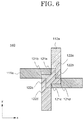
- FIG. 6 is an enlarged view of the region 140 shown in FIG. 5 .
- the wiring 111 a overlaps corner parts 122 a to 122 d of the bent part of the wiring 112 a.
- the wiring 112 a overlaps corner parts 121 a to 121 d of the bent part of the wiring 111 . That is, the wiring 112 a does not overlap the linear region of the wiring 111 a, and the wiring 111 a does not overlap the linear region of the wiring 112 a.
- the corner parts of a bent part mean two lines are folded and have an angle when viewed in a planar view.
- the bent part of one wiring overlaps the other wiring.
- the stress applied to the wiring 112 a can be dispersed in the region where the wiring 111 a and the wiring 112 a intersect. Therefore, disconnection of the wiring 112 a due to the wiring 111 a does not easily occur.
- it is difficult for the wiring 112 a to disconnect it is possible to improve reliability of the display device 100 .
- FIG. 7 is a drawing showing the region 140 A in which the structure of the region 140 shown in FIG. 6 is partially changed.
- a wiring 131 a is arranged in the first direction
- a wiring 132 a is arranged in the second direction.
- an insulating layer is arranged between the wiring 131 a and the wiring 132 a.
- the wiring 132 a overlaps a bent part of the wiring 131 a.
- the wiring 131 a overlaps a bent part of the wiring 132 a.
- the wiring 131 a overlaps the corner parts 142 a to 142 d of the bent part of the wiring 132 a.
- the wiring 132 a overlaps the corner parts 141 a to 141 d of the bent part of the wiring 131 .
- the corner parts 141 a to 141 d of the bent part of the wiring 131 a are rounded.
- the corners 142 a to 142 d of the bent part of the wiring 132 a are rounded.
- the fact that the corner parts are rounded means that the corner parts of the wiring are not a shape having an obtuse apex, but they have a curve.
- the two-dot chain line indicates a corner part of the bent part
- the solid line and the dotted line indicate the shapes of the actual wiring 131 a and the wiring 132 a.
- FIG. 8 is a drawing showing the region 140 B in which the structure of the region 140 shown in FIG. 6 is partially changed.
- a wiring 151 a is arranged in the first direction and the wiring 152 a is arranged in the second direction.
- an insulating layer is arranged between the wiring 151 a and the wiring 152 a.
- the bent part of the wiring 152 a overlaps the bent part of the wiring 151 a in the region 140 A where the wiring 151 a and the wiring 152 a intersect each other.
- the wiring 151 a overlaps the corner parts 162 a to 162 d of the bent part of the wiring 152 a.
- the wiring 152 a overlaps the corner parts 161 a to 161 d of the bent part of the wiring 151 .
- the corner parts 161 a to 161 d of the bent part of the wiring 151 a are chamfered.
- the corner parts 162 a to 162 d of the bent part of the wiring 152 a are chamfered.
- chamfered refers to a shape in which the corner part of the wiring is oblique.
- the corner parts 161 a to 161 d of the bent part of the wiring 151 a each have an apex with an obtuse angle
- the corner parts 162 a to 162 d of the bent part of the wiring 152 a each have an apex with an obtuse angle
- the two-dot chain line indicates the corner part of a bent part
- the solid line and the dotted line indicate the shapes of the actual wiring 151 a and the wiring 152 a.
- a display device 100 A having a structure which is partially different from the display device 100 shown in the first embodiment is explained while referring to FIG. 9 and FIG. 10 .
- An explanation of the same structure as that of the display device 100 shown in FIG. 1 is omitted.
- FIG. 9 is a plan view showing a structure of the display device 100 A according to the present embodiment.
- the structure of the folding region 120 A is partially different from the structure of the folding region 120 of the display device 100 shown in FIG. 1 .
- the structure of a wiring 181 and a wiring 182 is different from the structure of the wiring 111 and the wiring 112 shown in FIG. 1 .
- FIG. 10 is an enlarged view of a region 130 A shown in FIG. 9 .
- the wiring 181 a is arranged in the first direction and the wiring 182 a to 182 e is arranged in the second direction.
- an insulating layer is arranged between the wiring 181 a and the wirings 182 a to 182 e.
- the width m of the wiring 181 a is larger than the width n of the wiring 182 a. In this way, the width m of the wiring 181 which extend in the first direction may be different from the width n of the wirings 182 a to 182 e which extend in the second direction.
- the wiring 181 has at least one bent part.
- each of the wirings 182 a to 182 e has at least one bent part.
- the wiring 181 overlaps, for example, a bent part of the wiring 182 a in a region where the wiring 181 a and the wiring 182 a intersect each other.
- the wiring 181 a overlaps at least the corner parts 184 a and 184 b of the bent part of the wiring 182 a.
- the wiring 182 a overlaps the corner parts 183 a and 183 b of the bent part of the wiring 181 a.
- the corner parts 183 a, 183 b of the bent part of the wiring 181 a are rounded.
- the corner parts 184 a, 184 b of the bent part of the wiring 182 a are rounded.
- the fact that the corner parts are rounded means that the corner parts of the wiring are not a shape which has an obtuse apex but has a curve. That is, the wiring 181 a does not overlap a linear region of the wiring 182 a, and the wiring 182 a does not overlap a linear region of the wiring 181 a.
- a display device 100 B which has a structure partially different from the display device 100 described in the first embodiment is explained while referring to FIG. 11 to FIG. 15 . An explanation of the same structure as that of the display device 100 shown in FIG. 1 is omitted.
- the driver IC 105 is arranged in the periphery region 110 in the display device 100 shown in FIG. 1
- FIG. 11 an example in which the driver IC 105 is arranged on the flexible printed circuit 107 is shown.
- the display region 102 and the flexible printed circuit 107 are electrically connected by a plurality of wirings.
- FIG. 12 is a perspective view showing a state in which the display device 100 B is curved in one direction. Similar to the display device 100 shown in FIG. 3 , the display device 100 B is folded in the folding region 120 B. In this way, the substrate 101 is folded so that the driver IC 105 and the flexible printed circuit 107 overlap the rear side of the display region 102 . In addition, the display region 102 is curved in the direction of the arrow 303 .
- Stress occurs in the display region 102 by curving the display device 100 B in the direction of the arrow 303 . At this time, stress due to folding is concentrated in a region where a wiring extending in the first direction and a wiring extending in the second direction arranged in the display region 102 intersect each other.
- FIG. 3 is an enlarged view of a region 150 shown in FIG. 12 .
- Pixels 103 a to 103 f of 2 rows ⁇ 3 columns are arranged in the region 150 .
- FIG. 13 shows a conductive layer and a semiconductor layer which form the pixels 103 a to 103 f, and an illustration of an insulating film is omitted.
- a pixel 103 a includes a semiconductor layer 211 , a semiconductor layer 212 , wiring layers 213 and 215 , a conductive layer 214 , wiring layers 216 and 217 , conductive layers 218 and 219 and a pixel electrode 227 .
- the wiring layer 213 and the conductive layer 214 are arranged above the semiconductor layer 211 and the semiconductor layer 212 .
- the wiring layers 216 and 217 and conductive layers 218 and 219 are arranged above the wiring layers 213 and 215 and the conductive layer 214 .
- the wiring layer 215 is arranged above the wiring layers 216 and 217 .
- the pixel electrode 227 is arranged on the wiring layers 216 and 217 and the conductive layers 218 and 219 .
- the semiconductor layer 211 is connected to the wiring layer 217 and the conductive layer 218 .
- the conductive layer 218 is connected to the conductive layer 214 .
- the semiconductor layer 212 is connected to the wiring layer 215 and the conductive layer 219 .
- the wiring layer 215 is connected to the wiring layer 217 .
- the conductive layer 219 is connected to the pixel electrode 227 .
- a transistor 210 functions as a switching transistor.
- the wiring layer 213 functions as a gate and a scanning line of the transistor 210 .
- a region where the wiring layer 213 overlaps functions as a channel region of the transistor 210 .
- the wiring layer 217 functions as a source or drain of the transistor 210 and a signal line.
- the conductive layer 218 functions as a source or a drain.
- a transistor 220 functions as a drive transistor.
- the conductive layer 214 functions as a gate of the transistor 220 .
- a region where the conductive layer 214 overlaps functions as a channel region of the transistor 220 .
- the wiring layer 215 functions as a power supply line connected to one of the source and the drain of the transistor 220 .
- the conductive layer 219 is connected to the other of the transistor source or the drain and functions as connection wiring with a pixel electrode.
- the wiring layer 213 and the wiring layer 215 are arranged in the first direction (x direction) of the display region 102
- the wiring layer 216 and the wiring layer 217 are arranged in the second direction (y direction) intersecting the first direction of the display region 102 . That is, the wiring layer 213 intersects the wiring layer 217 , and the wiring layer 213 and the wiring layer 216 intersect each other.
- the wiring layer 215 intersects with the wiring layer 217 , and the wiring layer 215 and the wiring layer 216 intersect each other.
- FIG. 14 is an enlarged view of a region 160 where the wiring layers 213 and 215 extending in the first direction and the wiring layers 216 and 217 extending in the second direction intersect each other.
- An interlayer insulating film (not shown in the drawing) is arranged between the wiring layer 213 and the wiring layers 216 and 217 .
- an interlayer insulating film is also arranged between the wiring layers 216 and 217 and the wiring layer 215 .
- the wiring layer 215 is connected to the wiring layer 216 via an opening part 237 which is arranged in the interlayer insulating film.
- Each of the wiring layers 213 , 215 , 216 , and 217 includes two bent parts.
- the first bent part of the wiring layer 213 overlaps with the first bent part of the wiring layer 216 and the second bent part of the wiring layer 213 overlaps the first bent part of the wiring layer 217 .
- the first bent part of the wiring layer 215 overlaps the second bent part of the wiring layer 216
- the second bent part of the wiring layer 215 overlaps the second bent part of the wiring layer 217 .
- a corner part of the first bent part of the wiring layer 213 and the wiring layer 216 overlap in a region where the wiring layer 213 which extends in the first direction intersects with the wiring layer 216 which extends in the second direction.
- the substrate 101 is folded in the display region 102 , it is possible to further disperse the stress applied to the wiring layer 216 in the region where the wiring layer 213 and the wiring layer 216 intersect. Therefore, disconnection of the wiring layer 216 due to the wiring layer 213 does not easily occur.
- the wiring layer 216 does not easily disconnect, it is possible to improve the reliability of the display device 100 B.
- the corner parts of the bent parts of the wiring layers 213 , 215 , 216 and 217 may be rounded.
- the corner parts of the bent parts of the wiring layers 213 , 215 , 216 and 217 may be chamfered.
- chamfered refers to a shape in which the corner part of the wiring is oblique.
- the corner parts of the bent parts of the wiring layers 213 , 215 , 216 and 217 may each have an apex with an obtuse angle.
- FIG. 15 is a cross-sectional view of the display region 102 and the periphery region 110 in the display device 100 B shown in FIG. 11 .
- a flexible substrate such as polyimide
- a counter substrate 202 it is possible to use a flexible substrate such as polyimide as the substrate 101 and a counter substrate 202 .
- a bendable sheet display other resin materials may be used as a foldable sheet display as long as they have sufficient flexibility.
- An undercoat layer 203 is arranged above the substrate 101 .
- a silicon oxide film and a silicon nitride film can be used for the undercoat layer 203 .
- the undercoat layer 203 is arranged with a three-layer structure of, for example, a silicon oxide film, a silicon nitride film and a silicon oxide film.
- the silicon oxide film on the lowermost layer can improve adhesion to the substrate 101 .
- the silicon nitride film of the middle layer can suppress the entrance of moisture and impurities from the outside.
- the silicon oxide film on the uppermost layer can suppress hydrogen atoms contained in the silicon nitride film from diffusing into the semiconductor layer 211 .
- the undercoat layer 203 is not limited to the three-layer structure described above.
- the undercoat layer 203 may also have a stacked structure of four or more layers or may have a single layer structure or a two-layer structure.
- the pixel 103 includes a transistor 220 arranged above the undercoat layer 203 and a light emitting element 250 which is electrically connected to the transistor 220 .
- the transistor 220 includes the semiconductor layer 211 arranged above the undercoat layer 203 , a gate insulating film 221 covering the semiconductor layer 211 , and a conductive layer 214 arranged above the gate insulating film 221 .
- the conductive layer 214 functions as a gate electrode.
- An interlayer insulating film 222 is arranged above the transistor 220 to cover the conductive layer 214 .
- a wiring layer 215 and a conductive layer 219 are arranged above the interlayer insulating film 222 .
- the wiring layer 215 and the conductive layer 219 are connected to the semiconductor layer 211 via an opening part arranged in the interlayer insulating film 222 .
- each layer which forms the transistor 220 may be any known material and is not particularly limited. Polysilicon, amorphous silicon or an oxide semiconductor can be used as the semiconductor layer 211 . Silicon oxide or silicon nitride can be used as the gate insulating film 221 . In addition, a metal material such as copper, molybdenum, tantalum, tungsten, or aluminum may be used to form the conductive layer 214 . Silicon oxide or silicon nitride can be used as the interlayer insulating film 222 .
- the wiring layer 215 and the conductive layer 219 are each formed by a metal material such as copper, titanium, molybdenum or aluminum.
- a thin film transistor is shown as the transistor 220 .
- the transistor 220 is not limited to a thin film transistor, and any element may be used as long as it includes a current control function.
- an example in which an n-channel transistor is used for the transistor 220 is shown in FIG. 14 , a p-channel transistor may also be used.
- a planarization film 223 is arranged above the interlayer insulating film 222 , the wiring layer 215 and the conductive layer 219 .
- the planarization film 223 is formed using an organic resin material.
- organic resin material for example, polyimide, polyamide, acrylic or epoxy and the like can be used as the organic resin material. These materials are capable of film forming by a solution coating method and have the feature of a high flattening effect.
- the planarization film 223 is not arranged in the periphery region 110 .
- the planarization film 223 is arranged with an opening part.
- the conductive layer 219 is connected to a conductive layer 224 via the opening part of the planarization film 223 .
- a conductive layer 225 is arranged above the planarization film 223 .
- an indium oxide based transparent conductive film for example, ITO
- a zinc oxide based transparent conductive film for example, IZO, ZnO
- An insulating layer 226 is arranged above the planarization film 223 and the conductive layers 224 and 225 .
- the insulating layer 226 is formed using, for example, a silicon nitride film or a silicon oxide film.
- a pixel electrode 227 is arranged on the insulating layer 226 .
- the pixel electrode 227 is connected to the conductive layer 224 via an opening part arranged in the insulating layer 226 .
- An insulating layer 235 is arranged to cover the end part of the pixel electrode 227 .
- the insulating layer 235 is also called a partition wall or a bank. Similar to the planarization film 223 , photosensitive acrylic can be used as the insulating layer 235 . It is preferred that the insulating layer 235 be opened so that the pixel electrode 227 is exposed and the end part of the opening has a gentle tapered shape. When the end part of the opening has a steep shape, coverage defects of an organic layer 228 formed later occur.
- the insulating layer 226 is arranged with an opening part 230 , and the planarization film 223 and the insulating layer 235 are in contact with each other in the opening part 230 . In this way, moisture and gas desorbed from the planarization film 223 can be released through the insulating layer 235 by a heat treatment after the formation of the insulating layer 235 .
- the organic layer 228 is formed by stacking a hole transporting layer, a light emitting layer and an electron transporting layer in this order from the pixel electrode 227 side. These layers may be formed by vapor deposition or by coating formation after solvent dispersion. In addition, the organic layer 228 may be selectively formed for each subpixel or may be formed on the entire surface of the display region 102 . In the case of forming the organic layer 228 on the front surface, it is possible to adopt a structure in which white light is emitted in all pixels and a desired color wavelength part is extracted using a color filter (not shown in the drawing).
- a counter electrode 229 is formed after forming the organic layer 228 . Since a top emission structure is adopted in the present embodiment, it is necessary for the counter electrode 229 to have translucency. In the case when MgAg is used as the counter electrode 229 , it is formed using a thin film to the extent that light emitted from the organic layer 228 passes through.
- the light emitting element 250 is formed by the pixel electrode 227 , the organic layer 228 and the counter electrode 229 .
- the pixel electrode 227 serves as an anode and the counter electrode 229 serves as a cathode.
- the counter electrode 229 is formed above the display region 102 and across a cathode contact part arranged in the periphery region 110 . In the cathode contact part, the counter electrode 229 is connected to a wiring layer 252 via a conductive layer 254 and a conductive layer 253 and is electrically connected to the terminal 106 .
- a sealing film 240 is arranged above the counter electrode 229 .
- the sealing film 240 is arranged to suppress moisture entering from the outside from entering the organic layer 228 . Therefore, a material having high gas barrier properties is preferred as the sealing film 240 .
- FIG. 14 an example is shown in which the sealing film 240 is formed with a three-layer structure of an inorganic insulating layer 231 , an organic insulating layer 232 and an inorganic insulating layer 233 . It is preferred to use silicon nitride as the inorganic insulating layers 231 and 233 and an organic resin as the organic insulating layer 232 . Furthermore, a silicon oxide film or an amorphous silicon film may be arranged between the silicon nitride and the organic resin. In this way, adhesion can be improved.
- a filler 234 is arranged above the inorganic insulating layer 233 .
- acrylic, rubber, silicone, or urethane adhesive materials can be used for the filler 234 .
- a spacer may be arranged in the filler 234 in order to secure a gap between the substrate 101 and the counter substrate 202 . This spacer may be mixed into the filler 234 or may be formed from a resin or the like on the substrate 101 .
- an overcoat layer may be arranged having a flattening effect on the counter substrate 202 .
- a color filter corresponding to each color of RGB and a black matrix arranged between the color filters may be formed on a main surface (surface facing the substrate 101 ) on the counter substrate 202 .
- a color filter may be directly formed on the inorganic insulating layer 233 and the filler 234 may be formed above the color filter.
- the organic insulating layer 232 has a planarization effect, and each layer above the organic insulating layer 232 is formed flat. As a result, the organic insulating layer 232 is thick above the light emitting element 250 and thin above the insulating layer 235 .
- the wiring layer 252 and a conductive layer 255 form the terminal 106 .
- the conductive layer 255 is, for example, a film formed in the same step as the counter electrode 229 .
- the bent parts of the wiring layers overlap each other in a region where two wiring layers intersect. In this way, even when the substrate 101 is curved or folded in the display region 102 , it is possible to suppress stress concentration on an upper wiring layer due to a lower wiring layer. In this way, since disconnection of the wiring layer does not easily occur, it is possible to improve reliability of the display device 100 B.
- the wiring layer 251 and the wiring layer 252 intersect in the folding region 120 B. Similar to the previous embodiment, in the region where the wiring layer 251 and the wiring layer 252 intersect each other, the bent parts of the wiring layers overlap each other. In this way, even when the substrate 101 is bent or folded in the folding region 120 B, it is possible to suppress stress concentration on the wiring layer 252 due to the wiring layer 251 . In this way, disconnection of the wiring layer does not easily occur, and it is possible to improve the reliability of the folding region 120 B.
- resistance to bending or folding of the substrate 101 is improved not only in the folding region 120 B but also in the display region 102 of the display device 100 B.
- FIG. 16 is an equivalent circuit drawing of a pixel.
- the pixel 103 and the drive circuit 104 are connected by a plurality of wirings. Signals are provided from the drive circuit 104 to the pixel 103 via a gate light emission control scanning line BG, a reset control scanning line RG, a correction control scanning line CG, an initialization control scanning line IG, and a write control scanning line SG respectively.
- a light emission control transistor BCT, a correction transistor CCT, an initialization transistor IST, a write transistor SST, and a drive transistor DRT are arranged in the pixel 103 . Some of the transistors may be shared between a plurality of adjacent pixels.
- one reset transistor RST is arranged in each row in the periphery region 110 .
- a storage capacitor Cs may also be arranged between the gate and the source of the drive transistor DRT.
- a capacitor Cel is a parasitic capacitance between the anode and the cathode of the light emitting element OLED.
- a high potential side power supply PVDD is supplied to the anode of the light emitting element OLED via the light emission control transistor BCT, the correction transistor CCT and the drive transistor DRT.
- a low potential side power supply PVSS is supplied to the cathode of the light emitting element OLED.
- the light emission control transistor BCT, the correction transistor CCT, the initialization transistor IST and the write transistor SST function as switching elements for selecting conduction or non-conduction between two nodes.
- the drive transistor DRT functions as a current control element for controlling the value of a current which flows in the light emitting element OLED according to the voltage between the gate and the source.
- the light emission control transistor BCT, the correction transistor CCT, the initialization transistor IST and the write transistor SST are formed using a thin film transistor (TFT).
- TFT thin film transistor
- each of the plurality of TFTs used for a pixel is formed using an n-channel transistor, they may also be formed using a p-channel transistor. In the case when a p-channel transistor is used, connection of the power supply potential and holding capacity may be suitably adapted.
- FIG. 17 is a timing chart of the drive circuit 104 for driving a pixel shown in FIG. 16 .
- Each period shown by the time periods G 1 to G 4 is one horizontal period, and although omitted hereafter, continues until the last row.
- the time period indicated by T 0 to T 6 in FIG. 17 is explained in detail while referring to FIG. 16 .
- the light emitting element OLED continues a light emitting state of the previous frame until processing in a certain frame time period is started.
- the potential of the gate light emission control scanning line BG is a Low level (referred to as L level below)
- the potential of the reset control scanning line RG is a High level (referred to as H level below)
- the potential of the correction control scanning line CG is a H level.
- the light emission control transistor BCT is turned OFF, the correction transistor CCT is turned ON, and the reset transistor RST is turned ON.
- the current from the high potential power supply PVDD is blocked by the light emission control transistor BCT.
- the light emission of the light emitting element OLED is stopped, and an electric charge remaining within the pixel 103 is extracted through the reset transistor RST.
- the source of the drive transistor DRT is fixed to a reset potential Vrst.
- the reset potential Vrst is set to a lower potential than the emission start voltage of the light emitting element OLED with respect to the low potential side power supply PVSS.
- the potential of the initialization control scanning line IG becomes an H level, and the initialization transistor IST turns ON.
- the gate of the DRT is fixed to the initialization potential Vini via the initialization transistor IST.
- the initialization potential Vini is set to a larger potential than the threshold value of the drive transistor DRT with respect to the reset potential Vrst. That is, the drive transistor DRT is turned ON by this operation. However, since the light emission control transistor BCT is OFF, a current does not flow to the drive transistor DRT.
- the potential of the gate emission control scanning line BG becomes an H level and the potential of the reset control scanning line RG becomes an L level.
- the light emission control transistor BCT is turned ON and the reset transistor RST is turned OFF. Since the drive transistor DRT is in an ON state by the previous operation, a current is supplied from the light emitting control transistor BCT and the high potential side power supply PVDD to the drive transistor DRT through the correction transistor CCT. At this stage, a current does not flow since the voltage between the anode and the cathode of the light emitting element OLED does not exceed the light emission start voltage. Therefore, the source of the drive transistor DRT is charged by the current supplied from the high potential side power source PVDD, and the potential thereof increases.
- the gate potential of the drive transistor DRT is the initialization potential Vini. Therefore, when the potential of the source of the drive transistor DRT becomes (Vini-Vth), the drive transistor DRT turns OFF, and the increase of the potential stops. Since the threshold voltage Vth of the drive transistor DRT varies from pixel to pixel, the potential of the source of the drive transistor DRT when the increase of the potential stops varies depending on the pixel. That is, a voltage corresponding to the threshold voltage Vth of the drive transistor DRT is obtained in each pixel by this operation.
- the operations in the time periods T 1 to T 3 are executed in parallel for every two rows, the present invention is not limited to this. The operations may also be performed in sequence for every one row or in parallel for every three or more rows.
- the potential of the correction control scanning line CG is an L level
- the potential of the initialization control scanning line IG is an L level
- the potential of the write control scanning line SG is an H level.
- the correction transistor CCT is turned OFF
- the initialization transistor IST is turned ON
- the write transistor SST is turned ON.
- the potential of the image signal line Vsig is input to the gate of the drive transistor DRT.
- the gate potential of the drive transistor DRT changes from the initialization potential Vini to the potential of the image signal Vsig.
- the source potential of the drive transistor DRT is still (Vini-Vth), and as a result, the gate/source voltage of the drive transistor DRT becomes ⁇ Vsig-(Vini-Vth) ⁇ , which reflects the variation in threshold value between pixels.
- the potential of the correction control scanning line CG is an H level and the potential of the write control scanning line SG is a L level.
- the correction transistor CCT is turned ON and the write transistor SST is turned OFF.
- a current is supplied from the high potential side power supply PVDD to the drive transistor DRT through the light emission control transistor BCT and the correction transistor CCT.
- the drive transistor DRT supplies a current corresponding to the gate/source voltage which is set up to the previous stage to the light emitting element OLED, and the light emitting element OLED emits light with a luminosity corresponding to the current.
- the increase in the gate potential of the drive transistor DRT is slightly smaller than the increase of the potential on the anode side, since this value is known, the potential of the image signal line Vsig may be determined so that the desired current value can be obtained in the final voltage between the gate/source of the drive transistor DRT.
- a series of operations of the pixel is completed by the above. When these operations are completed from a first row to the final row, one pixel is displayed within one frame time period. Following this, the operations are repeated and display of an image is performed.
Landscapes
- Engineering & Computer Science (AREA)
- Physics & Mathematics (AREA)
- Microelectronics & Electronic Packaging (AREA)
- General Physics & Mathematics (AREA)
- Computer Hardware Design (AREA)
- Theoretical Computer Science (AREA)
- Power Engineering (AREA)
- Optics & Photonics (AREA)
- Condensed Matter Physics & Semiconductors (AREA)
- Devices For Indicating Variable Information By Combining Individual Elements (AREA)
- Liquid Crystal (AREA)
- Manufacturing & Machinery (AREA)
- Chemical & Material Sciences (AREA)
- Inorganic Chemistry (AREA)
- Electroluminescent Light Sources (AREA)
Applications Claiming Priority (2)
| Application Number | Priority Date | Filing Date | Title |
|---|---|---|---|
| JP2017-228227 | 2017-11-28 | ||
| JP2017228227A JP7013216B2 (ja) | 2017-11-28 | 2017-11-28 | 表示装置 |
Publications (2)
| Publication Number | Publication Date |
|---|---|
| US20190165333A1 US20190165333A1 (en) | 2019-05-30 |
| US10637008B2 true US10637008B2 (en) | 2020-04-28 |
Family
ID=66632745
Family Applications (1)
| Application Number | Title | Priority Date | Filing Date |
|---|---|---|---|
| US16/191,567 Active US10637008B2 (en) | 2017-11-28 | 2018-11-15 | Display device |
Country Status (2)
| Country | Link |
|---|---|
| US (1) | US10637008B2 (ja) |
| JP (1) | JP7013216B2 (ja) |
Cited By (7)
| Publication number | Priority date | Publication date | Assignee | Title |
|---|---|---|---|---|
| US11295664B2 (en) | 2020-03-11 | 2022-04-05 | Apple Inc. | Display-synchronized optical emitters and transceivers |
| US11327237B2 (en) | 2020-06-18 | 2022-05-10 | Apple Inc. | Display-adjacent optical emission or reception using optical fibers |
| US11422661B2 (en) | 2019-04-05 | 2022-08-23 | Apple Inc. | Sensing system for detection of light incident to a light emitting layer of an electronic device display |
| US11487859B2 (en) | 2020-07-31 | 2022-11-01 | Apple Inc. | Behind display polarized optical transceiver |
| US11527582B1 (en) | 2019-09-24 | 2022-12-13 | Apple Inc. | Display stack with integrated photodetectors |
| US11611058B2 (en) | 2019-09-24 | 2023-03-21 | Apple Inc. | Devices and systems for under display image sensor |
| US11839133B2 (en) | 2021-03-12 | 2023-12-05 | Apple Inc. | Organic photodetectors for in-cell optical sensing |
Families Citing this family (8)
| Publication number | Priority date | Publication date | Assignee | Title |
|---|---|---|---|---|
| CN109389906B (zh) * | 2018-11-26 | 2020-05-12 | 云谷(固安)科技有限公司 | 柔性显示面板和显示装置 |
| KR102664312B1 (ko) * | 2018-12-24 | 2024-05-09 | 엘지디스플레이 주식회사 | 플렉서블 디스플레이 장치 |
| US11056630B2 (en) * | 2019-02-13 | 2021-07-06 | Samsung Electronics Co., Ltd. | Display module having glass substrate on which side wirings are formed and manufacturing method of the same |
| CN110619816A (zh) * | 2019-08-19 | 2019-12-27 | 武汉华星光电半导体显示技术有限公司 | 显示面板及其制备方法、显示装置 |
| KR20210053381A (ko) * | 2019-11-01 | 2021-05-12 | 삼성디스플레이 주식회사 | 표시 장치 |
| KR20210067520A (ko) * | 2019-11-29 | 2021-06-08 | 엘지디스플레이 주식회사 | 투명표시패널 및 이의 제조 방법 |
| US11592873B2 (en) * | 2020-02-14 | 2023-02-28 | Apple Inc. | Display stack topologies for under-display optical transceivers |
| CN114120811A (zh) * | 2020-08-26 | 2022-03-01 | 深圳市柔宇科技股份有限公司 | 柔性显示面板及显示装置 |
Citations (3)
| Publication number | Priority date | Publication date | Assignee | Title |
|---|---|---|---|---|
| US20090051640A1 (en) | 2007-08-21 | 2009-02-26 | Masahiro Tanaka | Display Device |
| US20140216790A1 (en) * | 2013-02-05 | 2014-08-07 | David P. Trauernicht | Conductive micro-wire structure with offset intersections |
| US20170179210A1 (en) * | 2015-12-21 | 2017-06-22 | Japan Display Inc. | Display device |
Family Cites Families (4)
| Publication number | Priority date | Publication date | Assignee | Title |
|---|---|---|---|---|
| JP4753373B2 (ja) * | 2005-09-16 | 2011-08-24 | 株式会社半導体エネルギー研究所 | 表示装置及び表示装置の駆動方法 |
| KR102086644B1 (ko) * | 2013-12-31 | 2020-03-09 | 엘지디스플레이 주식회사 | 플렉서블표시장치 및 이의 제조방법 |
| TWI600946B (zh) * | 2015-04-07 | 2017-10-01 | 群創光電股份有限公司 | 顯示面板 |
| JP6412036B2 (ja) * | 2015-12-21 | 2018-10-24 | 株式会社ジャパンディスプレイ | 表示装置 |
-
2017
- 2017-11-28 JP JP2017228227A patent/JP7013216B2/ja active Active
-
2018
- 2018-11-15 US US16/191,567 patent/US10637008B2/en active Active
Patent Citations (4)
| Publication number | Priority date | Publication date | Assignee | Title |
|---|---|---|---|---|
| US20090051640A1 (en) | 2007-08-21 | 2009-02-26 | Masahiro Tanaka | Display Device |
| JP2009048007A (ja) | 2007-08-21 | 2009-03-05 | Hitachi Displays Ltd | 表示装置 |
| US20140216790A1 (en) * | 2013-02-05 | 2014-08-07 | David P. Trauernicht | Conductive micro-wire structure with offset intersections |
| US20170179210A1 (en) * | 2015-12-21 | 2017-06-22 | Japan Display Inc. | Display device |
Cited By (7)
| Publication number | Priority date | Publication date | Assignee | Title |
|---|---|---|---|---|
| US11422661B2 (en) | 2019-04-05 | 2022-08-23 | Apple Inc. | Sensing system for detection of light incident to a light emitting layer of an electronic device display |
| US11527582B1 (en) | 2019-09-24 | 2022-12-13 | Apple Inc. | Display stack with integrated photodetectors |
| US11611058B2 (en) | 2019-09-24 | 2023-03-21 | Apple Inc. | Devices and systems for under display image sensor |
| US11295664B2 (en) | 2020-03-11 | 2022-04-05 | Apple Inc. | Display-synchronized optical emitters and transceivers |
| US11327237B2 (en) | 2020-06-18 | 2022-05-10 | Apple Inc. | Display-adjacent optical emission or reception using optical fibers |
| US11487859B2 (en) | 2020-07-31 | 2022-11-01 | Apple Inc. | Behind display polarized optical transceiver |
| US11839133B2 (en) | 2021-03-12 | 2023-12-05 | Apple Inc. | Organic photodetectors for in-cell optical sensing |
Also Published As
| Publication number | Publication date |
|---|---|
| JP7013216B2 (ja) | 2022-01-31 |
| JP2019101062A (ja) | 2019-06-24 |
| US20190165333A1 (en) | 2019-05-30 |
Similar Documents
| Publication | Publication Date | Title |
|---|---|---|
| US10637008B2 (en) | Display device | |
| US11600794B2 (en) | Display device | |
| US11600679B2 (en) | Display apparatus | |
| US10340324B2 (en) | Organic light-emitting diode display | |
| US20190073951A1 (en) | Display device | |
| JP7118618B2 (ja) | 表示装置 | |
| US20160329391A1 (en) | Organic light-emitting diode display | |
| US9660009B2 (en) | Organic light emitting diode display | |
| US20160211308A1 (en) | Organic light emitting diode display | |
| US11417722B2 (en) | Display device including a low resistance cathode wiring | |
| US20160307981A1 (en) | Organic light-emitting diode display | |
| US11810491B2 (en) | TFT substrate including a non-rectangular active region | |
| US10431756B2 (en) | Display device | |
| US11289670B2 (en) | Display device and method of manufacturing display device | |
| WO2019107061A1 (ja) | 表示装置 | |
| JP7219830B2 (ja) | 素子基板 | |
| US11690251B2 (en) | Organic light-emitting display device having a gate insulating layer with controlled dielectric constants and method of manufacturing the same | |
| CN113394233A (zh) | 薄膜晶体管基底和包括该薄膜晶体管基底的显示装置 |
Legal Events
| Date | Code | Title | Description |
|---|---|---|---|
| AS | Assignment |
Owner name: JAPAN DISPLAY INC., JAPAN Free format text: ASSIGNMENT OF ASSIGNORS INTEREST;ASSIGNORS:HARADA, KEISUKE;KAJIYAMA, KENTA;REEL/FRAME:047511/0410 Effective date: 20181025 |
|
| FEPP | Fee payment procedure |
Free format text: ENTITY STATUS SET TO UNDISCOUNTED (ORIGINAL EVENT CODE: BIG.); ENTITY STATUS OF PATENT OWNER: LARGE ENTITY |
|
| STPP | Information on status: patent application and granting procedure in general |
Free format text: DOCKETED NEW CASE - READY FOR EXAMINATION |
|
| STPP | Information on status: patent application and granting procedure in general |
Free format text: NON FINAL ACTION MAILED |
|
| STPP | Information on status: patent application and granting procedure in general |
Free format text: RESPONSE TO NON-FINAL OFFICE ACTION ENTERED AND FORWARDED TO EXAMINER |
|
| STCF | Information on status: patent grant |
Free format text: PATENTED CASE |
|
| MAFP | Maintenance fee payment |
Free format text: PAYMENT OF MAINTENANCE FEE, 4TH YEAR, LARGE ENTITY (ORIGINAL EVENT CODE: M1551); ENTITY STATUS OF PATENT OWNER: LARGE ENTITY Year of fee payment: 4 |