US10586751B2 - Semiconductor package device and method of manufacturing the same - Google Patents
Semiconductor package device and method of manufacturing the same Download PDFInfo
- Publication number
- US10586751B2 US10586751B2 US15/668,633 US201715668633A US10586751B2 US 10586751 B2 US10586751 B2 US 10586751B2 US 201715668633 A US201715668633 A US 201715668633A US 10586751 B2 US10586751 B2 US 10586751B2
- Authority
- US
- United States
- Prior art keywords
- electrical component
- back surface
- semiconductor package
- package device
- substrate
- Prior art date
- Legal status (The legal status is an assumption and is not a legal conclusion. Google has not performed a legal analysis and makes no representation as to the accuracy of the status listed.)
- Active
Links
- 239000004065 semiconductor Substances 0.000 title claims abstract description 60
- 238000004519 manufacturing process Methods 0.000 title description 17
- 239000000758 substrate Substances 0.000 claims abstract description 39
- 239000002061 nanopillar Substances 0.000 claims description 4
- 238000000034 method Methods 0.000 description 15
- 239000000463 material Substances 0.000 description 9
- KRHYYFGTRYWZRS-UHFFFAOYSA-N Fluorane Chemical compound F KRHYYFGTRYWZRS-UHFFFAOYSA-N 0.000 description 6
- VYPSYNLAJGMNEJ-UHFFFAOYSA-N Silicium dioxide Chemical compound O=[Si]=O VYPSYNLAJGMNEJ-UHFFFAOYSA-N 0.000 description 6
- SQGYOTSLMSWVJD-UHFFFAOYSA-N silver(1+) nitrate Chemical compound [Ag+].[O-]N(=O)=O SQGYOTSLMSWVJD-UHFFFAOYSA-N 0.000 description 6
- 239000000853 adhesive Substances 0.000 description 5
- 230000001070 adhesive effect Effects 0.000 description 5
- 150000001875 compounds Chemical class 0.000 description 4
- 238000005530 etching Methods 0.000 description 4
- 238000000465 moulding Methods 0.000 description 4
- RYGMFSIKBFXOCR-UHFFFAOYSA-N Copper Chemical compound [Cu] RYGMFSIKBFXOCR-UHFFFAOYSA-N 0.000 description 3
- 239000004020 conductor Substances 0.000 description 3
- 239000011889 copper foil Substances 0.000 description 3
- 230000017525 heat dissipation Effects 0.000 description 3
- 229920002120 photoresistant polymer Polymers 0.000 description 3
- 239000000377 silicon dioxide Substances 0.000 description 3
- 229910052709 silver Inorganic materials 0.000 description 3
- 239000004332 silver Substances 0.000 description 3
- 239000004642 Polyimide Substances 0.000 description 2
- 229920006336 epoxy molding compound Polymers 0.000 description 2
- 239000003822 epoxy resin Substances 0.000 description 2
- 239000000945 filler Substances 0.000 description 2
- 238000012986 modification Methods 0.000 description 2
- 230000004048 modification Effects 0.000 description 2
- QPJSUIGXIBEQAC-UHFFFAOYSA-N n-(2,4-dichloro-5-propan-2-yloxyphenyl)acetamide Chemical compound CC(C)OC1=CC(NC(C)=O)=C(Cl)C=C1Cl QPJSUIGXIBEQAC-UHFFFAOYSA-N 0.000 description 2
- 239000002245 particle Substances 0.000 description 2
- 150000002989 phenols Chemical class 0.000 description 2
- 229920000647 polyepoxide Polymers 0.000 description 2
- 229920001721 polyimide Polymers 0.000 description 2
- 229920001296 polysiloxane Polymers 0.000 description 2
- -1 silver ions Chemical class 0.000 description 2
- XUIMIQQOPSSXEZ-UHFFFAOYSA-N Silicon Chemical compound [Si] XUIMIQQOPSSXEZ-UHFFFAOYSA-N 0.000 description 1
- BQCADISMDOOEFD-UHFFFAOYSA-N Silver Chemical compound [Ag] BQCADISMDOOEFD-UHFFFAOYSA-N 0.000 description 1
- 239000003990 capacitor Substances 0.000 description 1
- 230000000052 comparative effect Effects 0.000 description 1
- 239000002131 composite material Substances 0.000 description 1
- 238000005336 cracking Methods 0.000 description 1
- 238000007598 dipping method Methods 0.000 description 1
- 238000006073 displacement reaction Methods 0.000 description 1
- 238000007772 electroless plating Methods 0.000 description 1
- 238000009713 electroplating Methods 0.000 description 1
- 239000003365 glass fiber Substances 0.000 description 1
- 238000009413 insulation Methods 0.000 description 1
- 150000002500 ions Chemical class 0.000 description 1
- VCJMYUPGQJHHFU-UHFFFAOYSA-N iron(III) nitrate Inorganic materials [Fe+3].[O-][N+]([O-])=O.[O-][N+]([O-])=O.[O-][N+]([O-])=O VCJMYUPGQJHHFU-UHFFFAOYSA-N 0.000 description 1
- 239000002184 metal Substances 0.000 description 1
- 229910052751 metal Inorganic materials 0.000 description 1
- 239000000203 mixture Substances 0.000 description 1
- 239000007800 oxidant agent Substances 0.000 description 1
- 238000007747 plating Methods 0.000 description 1
- 238000006479 redox reaction Methods 0.000 description 1
- 229910052710 silicon Inorganic materials 0.000 description 1
- 239000010703 silicon Substances 0.000 description 1
- 235000012239 silicon dioxide Nutrition 0.000 description 1
- 229910000679 solder Inorganic materials 0.000 description 1
- 238000004544 sputter deposition Methods 0.000 description 1
Images
Classifications
-
- H—ELECTRICITY
- H01—ELECTRIC ELEMENTS
- H01L—SEMICONDUCTOR DEVICES NOT COVERED BY CLASS H10
- H01L23/00—Details of semiconductor or other solid state devices
- H01L23/28—Encapsulations, e.g. encapsulating layers, coatings, e.g. for protection
- H01L23/31—Encapsulations, e.g. encapsulating layers, coatings, e.g. for protection characterised by the arrangement or shape
- H01L23/3157—Partial encapsulation or coating
-
- H—ELECTRICITY
- H01—ELECTRIC ELEMENTS
- H01L—SEMICONDUCTOR DEVICES NOT COVERED BY CLASS H10
- H01L23/00—Details of semiconductor or other solid state devices
- H01L23/34—Arrangements for cooling, heating, ventilating or temperature compensation ; Temperature sensing arrangements
- H01L23/36—Selection of materials, or shaping, to facilitate cooling or heating, e.g. heatsinks
- H01L23/367—Cooling facilitated by shape of device
- H01L23/3677—Wire-like or pin-like cooling fins or heat sinks
-
- H—ELECTRICITY
- H01—ELECTRIC ELEMENTS
- H01L—SEMICONDUCTOR DEVICES NOT COVERED BY CLASS H10
- H01L21/00—Processes or apparatus adapted for the manufacture or treatment of semiconductor or solid state devices or of parts thereof
- H01L21/02—Manufacture or treatment of semiconductor devices or of parts thereof
- H01L21/04—Manufacture or treatment of semiconductor devices or of parts thereof the devices having at least one potential-jump barrier or surface barrier, e.g. PN junction, depletion layer or carrier concentration layer
- H01L21/50—Assembly of semiconductor devices using processes or apparatus not provided for in a single one of the subgroups H01L21/06 - H01L21/326, e.g. sealing of a cap to a base of a container
- H01L21/56—Encapsulations, e.g. encapsulation layers, coatings
- H01L21/561—Batch processing
-
- H—ELECTRICITY
- H01—ELECTRIC ELEMENTS
- H01L—SEMICONDUCTOR DEVICES NOT COVERED BY CLASS H10
- H01L21/00—Processes or apparatus adapted for the manufacture or treatment of semiconductor or solid state devices or of parts thereof
- H01L21/02—Manufacture or treatment of semiconductor devices or of parts thereof
- H01L21/04—Manufacture or treatment of semiconductor devices or of parts thereof the devices having at least one potential-jump barrier or surface barrier, e.g. PN junction, depletion layer or carrier concentration layer
- H01L21/50—Assembly of semiconductor devices using processes or apparatus not provided for in a single one of the subgroups H01L21/06 - H01L21/326, e.g. sealing of a cap to a base of a container
- H01L21/56—Encapsulations, e.g. encapsulation layers, coatings
- H01L21/568—Temporary substrate used as encapsulation process aid
-
- H—ELECTRICITY
- H01—ELECTRIC ELEMENTS
- H01L—SEMICONDUCTOR DEVICES NOT COVERED BY CLASS H10
- H01L21/00—Processes or apparatus adapted for the manufacture or treatment of semiconductor or solid state devices or of parts thereof
- H01L21/67—Apparatus specially adapted for handling semiconductor or electric solid state devices during manufacture or treatment thereof; Apparatus specially adapted for handling wafers during manufacture or treatment of semiconductor or electric solid state devices or components ; Apparatus not specifically provided for elsewhere
- H01L21/683—Apparatus specially adapted for handling semiconductor or electric solid state devices during manufacture or treatment thereof; Apparatus specially adapted for handling wafers during manufacture or treatment of semiconductor or electric solid state devices or components ; Apparatus not specifically provided for elsewhere for supporting or gripping
- H01L21/6835—Apparatus specially adapted for handling semiconductor or electric solid state devices during manufacture or treatment thereof; Apparatus specially adapted for handling wafers during manufacture or treatment of semiconductor or electric solid state devices or components ; Apparatus not specifically provided for elsewhere for supporting or gripping using temporarily an auxiliary support
-
- H—ELECTRICITY
- H01—ELECTRIC ELEMENTS
- H01L—SEMICONDUCTOR DEVICES NOT COVERED BY CLASS H10
- H01L23/00—Details of semiconductor or other solid state devices
- H01L23/28—Encapsulations, e.g. encapsulating layers, coatings, e.g. for protection
- H01L23/31—Encapsulations, e.g. encapsulating layers, coatings, e.g. for protection characterised by the arrangement or shape
- H01L23/3107—Encapsulations, e.g. encapsulating layers, coatings, e.g. for protection characterised by the arrangement or shape the device being completely enclosed
- H01L23/3121—Encapsulations, e.g. encapsulating layers, coatings, e.g. for protection characterised by the arrangement or shape the device being completely enclosed a substrate forming part of the encapsulation
- H01L23/3128—Encapsulations, e.g. encapsulating layers, coatings, e.g. for protection characterised by the arrangement or shape the device being completely enclosed a substrate forming part of the encapsulation the substrate having spherical bumps for external connection
-
- H—ELECTRICITY
- H01—ELECTRIC ELEMENTS
- H01L—SEMICONDUCTOR DEVICES NOT COVERED BY CLASS H10
- H01L23/00—Details of semiconductor or other solid state devices
- H01L23/34—Arrangements for cooling, heating, ventilating or temperature compensation ; Temperature sensing arrangements
- H01L23/36—Selection of materials, or shaping, to facilitate cooling or heating, e.g. heatsinks
- H01L23/367—Cooling facilitated by shape of device
-
- H—ELECTRICITY
- H01—ELECTRIC ELEMENTS
- H01L—SEMICONDUCTOR DEVICES NOT COVERED BY CLASS H10
- H01L24/00—Arrangements for connecting or disconnecting semiconductor or solid-state bodies; Methods or apparatus related thereto
- H01L24/01—Means for bonding being attached to, or being formed on, the surface to be connected, e.g. chip-to-package, die-attach, "first-level" interconnects; Manufacturing methods related thereto
- H01L24/18—High density interconnect [HDI] connectors; Manufacturing methods related thereto
- H01L24/19—Manufacturing methods of high density interconnect preforms
-
- H—ELECTRICITY
- H01—ELECTRIC ELEMENTS
- H01L—SEMICONDUCTOR DEVICES NOT COVERED BY CLASS H10
- H01L24/00—Arrangements for connecting or disconnecting semiconductor or solid-state bodies; Methods or apparatus related thereto
- H01L24/01—Means for bonding being attached to, or being formed on, the surface to be connected, e.g. chip-to-package, die-attach, "first-level" interconnects; Manufacturing methods related thereto
- H01L24/18—High density interconnect [HDI] connectors; Manufacturing methods related thereto
- H01L24/20—Structure, shape, material or disposition of high density interconnect preforms
-
- H—ELECTRICITY
- H01—ELECTRIC ELEMENTS
- H01L—SEMICONDUCTOR DEVICES NOT COVERED BY CLASS H10
- H01L29/00—Semiconductor devices adapted for rectifying, amplifying, oscillating or switching, or capacitors or resistors with at least one potential-jump barrier or surface barrier, e.g. PN junction depletion layer or carrier concentration layer; Details of semiconductor bodies or of electrodes thereof ; Multistep manufacturing processes therefor
- H01L29/02—Semiconductor bodies ; Multistep manufacturing processes therefor
- H01L29/06—Semiconductor bodies ; Multistep manufacturing processes therefor characterised by their shape; characterised by the shapes, relative sizes, or dispositions of the semiconductor regions ; characterised by the concentration or distribution of impurities within semiconductor regions
- H01L29/0657—Semiconductor bodies ; Multistep manufacturing processes therefor characterised by their shape; characterised by the shapes, relative sizes, or dispositions of the semiconductor regions ; characterised by the concentration or distribution of impurities within semiconductor regions characterised by the shape of the body
- H01L29/0665—Semiconductor bodies ; Multistep manufacturing processes therefor characterised by their shape; characterised by the shapes, relative sizes, or dispositions of the semiconductor regions ; characterised by the concentration or distribution of impurities within semiconductor regions characterised by the shape of the body the shape of the body defining a nanostructure
- H01L29/0669—Nanowires or nanotubes
- H01L29/0676—Nanowires or nanotubes oriented perpendicular or at an angle to a substrate
-
- H—ELECTRICITY
- H01—ELECTRIC ELEMENTS
- H01L—SEMICONDUCTOR DEVICES NOT COVERED BY CLASS H10
- H01L2221/00—Processes or apparatus adapted for the manufacture or treatment of semiconductor or solid state devices or of parts thereof covered by H01L21/00
- H01L2221/67—Apparatus for handling semiconductor or electric solid state devices during manufacture or treatment thereof; Apparatus for handling wafers during manufacture or treatment of semiconductor or electric solid state devices or components; Apparatus not specifically provided for elsewhere
- H01L2221/683—Apparatus for handling semiconductor or electric solid state devices during manufacture or treatment thereof; Apparatus for handling wafers during manufacture or treatment of semiconductor or electric solid state devices or components; Apparatus not specifically provided for elsewhere for supporting or gripping
- H01L2221/68304—Apparatus for handling semiconductor or electric solid state devices during manufacture or treatment thereof; Apparatus for handling wafers during manufacture or treatment of semiconductor or electric solid state devices or components; Apparatus not specifically provided for elsewhere for supporting or gripping using temporarily an auxiliary support
- H01L2221/68372—Apparatus for handling semiconductor or electric solid state devices during manufacture or treatment thereof; Apparatus for handling wafers during manufacture or treatment of semiconductor or electric solid state devices or components; Apparatus not specifically provided for elsewhere for supporting or gripping using temporarily an auxiliary support used to support a device or wafer when forming electrical connections thereto
-
- H—ELECTRICITY
- H01—ELECTRIC ELEMENTS
- H01L—SEMICONDUCTOR DEVICES NOT COVERED BY CLASS H10
- H01L2224/00—Indexing scheme for arrangements for connecting or disconnecting semiconductor or solid-state bodies and methods related thereto as covered by H01L24/00
- H01L2224/01—Means for bonding being attached to, or being formed on, the surface to be connected, e.g. chip-to-package, die-attach, "first-level" interconnects; Manufacturing methods related thereto
- H01L2224/02—Bonding areas; Manufacturing methods related thereto
- H01L2224/04—Structure, shape, material or disposition of the bonding areas prior to the connecting process
- H01L2224/04105—Bonding areas formed on an encapsulation of the semiconductor or solid-state body, e.g. bonding areas on chip-scale packages
-
- H—ELECTRICITY
- H01—ELECTRIC ELEMENTS
- H01L—SEMICONDUCTOR DEVICES NOT COVERED BY CLASS H10
- H01L2224/00—Indexing scheme for arrangements for connecting or disconnecting semiconductor or solid-state bodies and methods related thereto as covered by H01L24/00
- H01L2224/01—Means for bonding being attached to, or being formed on, the surface to be connected, e.g. chip-to-package, die-attach, "first-level" interconnects; Manufacturing methods related thereto
- H01L2224/10—Bump connectors; Manufacturing methods related thereto
- H01L2224/12—Structure, shape, material or disposition of the bump connectors prior to the connecting process
- H01L2224/12105—Bump connectors formed on an encapsulation of the semiconductor or solid-state body, e.g. bumps on chip-scale packages
-
- H—ELECTRICITY
- H01—ELECTRIC ELEMENTS
- H01L—SEMICONDUCTOR DEVICES NOT COVERED BY CLASS H10
- H01L2224/00—Indexing scheme for arrangements for connecting or disconnecting semiconductor or solid-state bodies and methods related thereto as covered by H01L24/00
- H01L2224/01—Means for bonding being attached to, or being formed on, the surface to be connected, e.g. chip-to-package, die-attach, "first-level" interconnects; Manufacturing methods related thereto
- H01L2224/18—High density interconnect [HDI] connectors; Manufacturing methods related thereto
-
- H—ELECTRICITY
- H01—ELECTRIC ELEMENTS
- H01L—SEMICONDUCTOR DEVICES NOT COVERED BY CLASS H10
- H01L2224/00—Indexing scheme for arrangements for connecting or disconnecting semiconductor or solid-state bodies and methods related thereto as covered by H01L24/00
- H01L2224/93—Batch processes
- H01L2224/95—Batch processes at chip-level, i.e. with connecting carried out on a plurality of singulated devices, i.e. on diced chips
- H01L2224/96—Batch processes at chip-level, i.e. with connecting carried out on a plurality of singulated devices, i.e. on diced chips the devices being encapsulated in a common layer, e.g. neo-wafer or pseudo-wafer, said common layer being separable into individual assemblies after connecting
-
- H—ELECTRICITY
- H01—ELECTRIC ELEMENTS
- H01L—SEMICONDUCTOR DEVICES NOT COVERED BY CLASS H10
- H01L24/00—Arrangements for connecting or disconnecting semiconductor or solid-state bodies; Methods or apparatus related thereto
- H01L24/93—Batch processes
- H01L24/95—Batch processes at chip-level, i.e. with connecting carried out on a plurality of singulated devices, i.e. on diced chips
- H01L24/96—Batch processes at chip-level, i.e. with connecting carried out on a plurality of singulated devices, i.e. on diced chips the devices being encapsulated in a common layer, e.g. neo-wafer or pseudo-wafer, said common layer being separable into individual assemblies after connecting
-
- H—ELECTRICITY
- H01—ELECTRIC ELEMENTS
- H01L—SEMICONDUCTOR DEVICES NOT COVERED BY CLASS H10
- H01L2924/00—Indexing scheme for arrangements or methods for connecting or disconnecting semiconductor or solid-state bodies as covered by H01L24/00
- H01L2924/10—Details of semiconductor or other solid state devices to be connected
- H01L2924/1015—Shape
- H01L2924/10155—Shape being other than a cuboid
- H01L2924/10156—Shape being other than a cuboid at the periphery
-
- H—ELECTRICITY
- H01—ELECTRIC ELEMENTS
- H01L—SEMICONDUCTOR DEVICES NOT COVERED BY CLASS H10
- H01L2924/00—Indexing scheme for arrangements or methods for connecting or disconnecting semiconductor or solid-state bodies as covered by H01L24/00
- H01L2924/10—Details of semiconductor or other solid state devices to be connected
- H01L2924/1015—Shape
- H01L2924/10155—Shape being other than a cuboid
- H01L2924/10158—Shape being other than a cuboid at the passive surface
-
- H—ELECTRICITY
- H01—ELECTRIC ELEMENTS
- H01L—SEMICONDUCTOR DEVICES NOT COVERED BY CLASS H10
- H01L2924/00—Indexing scheme for arrangements or methods for connecting or disconnecting semiconductor or solid-state bodies as covered by H01L24/00
- H01L2924/15—Details of package parts other than the semiconductor or other solid state devices to be connected
- H01L2924/181—Encapsulation
- H01L2924/1815—Shape
- H01L2924/1816—Exposing the passive side of the semiconductor or solid-state body
- H01L2924/18162—Exposing the passive side of the semiconductor or solid-state body of a chip with build-up interconnect
Definitions
- the present disclosure relates generally to a semiconductor package device and a method of manufacturing the same. More particularly, the present disclosure relates to a semiconductor package device including a heat dissipation structure and a method of manufacturing the same.
- a heat sink or spreader is bonded to the backside of the chip or die for heat dissipation.
- the use of the heat sink or spreader can increase the manufacturing cost and the thickness of the die or chip.
- a semiconductor package device comprises a substrate, an electrical component and a package body.
- the electrical component is disposed on the substrate.
- the electrical component has an active surface facing toward the substrate and a back surface opposite to the active surface.
- the back surface has a first portion and a second portion surrounding the first portion.
- the first portion of the back surface of the electrical component includes a plurality of pillars.
- the package body is disposed on the substrate. The package body encapsulates the electrical component and exposes the back surface of the electrical component.
- a semiconductor package device comprises a substrate, an electrical component and a package body.
- the electrical component is disposed on the substrate.
- the electrical component has an active surface facing toward the substrate and a back surface opposite to the active surface.
- the back surface has a first portion and a second portion surrounding the first portion.
- the first portion of the back surface of the electrical component defines a plurality of holes.
- the package body is disposed on the substrate. The package body encapsulates the electrical component and exposes the back surface of the electrical component.
- a semiconductor package device comprises a substrate, an electrical component and a package body.
- the electrical component is disposed on the substrate.
- the electrical component has an active surface facing toward the substrate, a back surface opposite to the active surface and a lateral surface extending between the active surface and the back surface.
- the lateral surface of the electrical component defines a plurality of holes.
- the package body is disposed on the substrate. The package body encapsulates the electrical component and exposes the back surface and the plurality of holes of the lateral surface of the electrical component.
- FIG. 1A illustrates a cross-sectional view of a semiconductor package device in accordance with some embodiments of the present disclosure
- FIG. 1B illustrates an enlarged view of a portion of the semiconductor package device shown in FIG. 1A in accordance with some embodiments of the present disclosure
- FIG. 1C illustrates an enlarged view of a portion of the semiconductor package device shown in FIG. 1A in accordance with some embodiments of the present disclosure
- FIG. 1D illustrates an enlarged view of a portion of the semiconductor package device shown in FIG. 1A in accordance with some embodiments of the present disclosure
- FIG. 1E illustrates an enlarged view of a portion of the semiconductor package device shown in FIG. 1A in accordance with some embodiments of the present disclosure
- FIG. 2A illustrates one or more stages of a method of manufacturing a semiconductor package device in accordance with some embodiments of the present disclosure
- FIG. 2B illustrates one or more stages of a method of manufacturing a semiconductor package device in accordance with some embodiments of the present disclosure
- FIG. 2C illustrates one or more stages of a method of manufacturing a semiconductor package device in accordance with some embodiments of the present disclosure
- FIG. 2C ′ illustrates one or more stages of a method of manufacturing a semiconductor package device in accordance with some embodiments of the present disclosure
- FIG. 2D illustrates one or more stages of a method of manufacturing a semiconductor package device in accordance with some embodiments of the present disclosure
- FIG. 2D ′ illustrates one or more stages of a method of manufacturing a semiconductor package device in accordance with some embodiments of the present disclosure
- FIG. 3A illustrates one or more stages of a method of manufacturing a semiconductor package device in accordance with some embodiments of the present disclosure
- FIG. 3B illustrates one or more stages of a method of manufacturing a semiconductor package device in accordance with some embodiments of the present disclosure
- FIG. 3C illustrates one or more stages of a method of manufacturing a semiconductor package device in accordance with some embodiments of the present disclosure
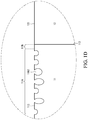
- FIG. 4A illustrates a perspective view of a portion of an electrical component in accordance with some embodiments of the present disclosure.
- FIG. 4B illustrates a perspective view of a portion of an electrical component in accordance with some embodiments of the present disclosure.
- a semiconductor package device includes an electrical component (e.g., a die or a chip).
- an electrical component e.g., a die or a chip.
- a plurality of features in nanoscale are disposed on a surface of the electrical component to improve heat dissipation of the semiconductor package device.
- the nanoscale features perform as heat dissipaters and replace a comparative heat sink, reducing manufacturing cost and an overall thickness of the semiconductor package device.
- FIG. 1A illustrates a cross-sectional view of a semiconductor package device 1 A in accordance with some embodiments of the present disclosure.
- the semiconductor package device 1 A includes a substrate 10 , an electrical component (e.g., a die or a chip) 11 and a package body 12 .
- the substrate 10 may be, for example, a printed circuit board (PCB), such as a paper-based copper foil laminate, a composite copper foil laminate, a polymer-impregnated glass-fiber-based copper foil laminate, or a combination of two or more thereof.
- the substrate 10 may include an interconnection structure 10 r , such as a redistribution layer (RDL).
- the substrate 10 has a top surface 101 (also referred to as “first surface”) and a bottom surface 102 (also referred to as “second surface”) opposite to the top surface 101 .
- One or more electrical contacts 10 b are disposed on the bottom surface 102 of the substrate 10 and electrically connected to the top surface 101 of the substrate 10 through the interconnection structure 10 r .
- the electrical contacts 10 b are Controlled Collapse Chip Connection (C4) bumps, solder balls, Land Grid Array (LGA), or a combination of two or more thereof.
- C4 Controlled Collapse Chip Connection
- LGA Land Grid Array
- the electrical component 11 is disposed on the top surface 101 of the substrate 10 .
- the electrical component 11 has an active surface 111 facing toward the top surface 101 of the substrate 10 , a back surface 112 (also referred to as backside) opposite to the active surface 111 and a lateral surface 113 extending between the active surface 111 and the back surface 112 .
- the electrical component 11 may include a semiconductor substrate, one or more integrated circuit devices and one or more overlying interconnection structures therein.
- the integrated circuit devices may include active devices such as transistors and/or passive devices such resistors, capacitors, inductors, or a combination of two or more thereof.
- the package body 12 is disposed on the top surface 101 of the substrate 10 and covers the top surface 101 of the substrate 10 and a portion of the electrical component 11 .
- the back surface 112 of the electrical component 11 is exposed from the package body 12 .
- a portion of the lateral surface 113 of the electrical component 11 is exposed from the package body 12 .
- the lateral surface 113 of the electrical component 11 may be completely covered by the package body 12 .
- the package body 12 includes an epoxy resin having fillers, a molding compound (e.g., an epoxy molding compound or other molding compound), a polyimide, a phenolic compound or material, a material with a silicone dispersed therein, or a combination of two or more thereof.
- FIG. 1B illustrates an enlarged view of a portion of the semiconductor package device 1 shown in FIG. 1A marked by the circle A, in accordance with some embodiments of the present disclosure.
- the back surface 112 of the electrical component 11 has a first portion 11 A and a second portion 11 B surrounding the first portion 11 A.
- the first portion 11 A may be a central portion of the back surface 112 of the electrical component 11 and the second portion 11 B may be the edges of the back surface 112 of the electrical component 11 .
- the first portion 11 A of the back surface 112 of the electrical component 11 includes a plurality of pillars 11 p .
- the pillars 11 p are nanopillars.
- the height and the width of each of the pillars 11 p is in nanoscale.
- the pillars 11 p and the back surface 112 of the electrical component 11 are formed of the same material.
- the pillars 11 p are parts of the back surface 112 of the electrical component 11 and are integrally formed as a monolithic or homogeneous structure with a remaining part of the electrical component 11 .
- the heights of the pillars 11 p are different from each other.
- Pillars sized differently from the nanoscale are also encompassed by this disclosure, such as having heights and/or widths greater than 100 nanometers (nm) and up to 500 nm or greater.
- an interface between the electrical component 11 and the package body 12 is substantially coplanar with or lower than the second portion 11 B of the back surface 112 of the electrical component 11 to avoid cracking at the edge of the top surface 112 of the electrical component 11 .
- the first portion 11 A of the back surface 112 of the electrical component 11 is not coplanar with the second portion 11 B of the back surface 112 of the electrical component 11 .
- the first portion 11 A of the back surface 112 of the electrical component 11 can be higher than, substantially coplanar with or lower than an interface between the electrical component 11 and the package body 12 depending on various arrangements of different embodiments.
- the top surface 121 of the package body 12 is substantially planar. In other embodiments, for example, as shown in FIG. 1E , the top surface 121 ′ of the package body 12 may be arc-shaped.
- nanopillars 11 p By forming nanopillars 11 p on the back surface 112 of the electrical component 11 that is exposed from the package body 12 , the performance of the heat dispassion of the electrical component 11 can be improved. In addition, since no heat sink is included in the semiconductor package device 1 , the manufacturing cost and the thickness of the semiconductor package device 1 can be reduced.
- FIG. 1C illustrates an enlarged view of a portion of the semiconductor package device 1 shown in FIG. 1A marked by the circle A, in accordance with some embodiments of the present disclosure.
- the top surface 121 of the package body 12 is lower than the second portion 11 B of the back surface 112 of the electrical component 11 to expose a portion of the lateral surface 113 of the electrical component 11 .
- the exposed portion of the lateral surface 113 of the electrical component 11 defines a plurality of holes (or notches) 11 h 1 .
- the holes 11 h 1 are nanoholes.
- the depth and the width of each of the holes 11 h 1 is in nanoscale. Holes sized differently from the nanoscale are also encompassed by this disclosure, such as having depths and/or widths greater than 100 nm and up to 500 nm or greater.
- FIG. 1D illustrates an enlarged view of a portion of the semiconductor package device 1 shown in FIG. 1A marked by the circle A, in accordance with some embodiments of the present disclosure.
- the structure shown in FIG. 1D is similar to that shown in FIG. 1B , except that in the structure shown in FIG. 1D , the first portion 11 A of the back surface 112 of the electrical component 11 defines a plurality of holes (or notches) 11 h 2 .
- the holes 11 h 2 are nanoholes.
- the depth and the width of each of the holes 11 h 2 is in nanoscale.
- the depths or the widths of the holes 11 h 2 are different from each other.
- nanoholes 11 h 2 By forming nanoholes 11 h 2 on the back surface 112 of the electrical component 11 that is exposed from the package body 12 , the performance of the heat dispassion of the electrical component 11 can be improved. In addition, since no heat sink is included in the semiconductor package device 1 , the manufacturing cost and the thickness of the semiconductor package device 1 can be reduced.
- FIGS. 2A, 2B, 2C, 2C ′, 2 D and 2 D′ are cross-sectional views of a semiconductor structure fabricated at various stages, in accordance with some embodiments of the present disclosure. Various figures have been simplified for a better understanding of the aspects of the present disclosure.
- a carrier 29 with an adhesive 29 a e.g., a tape
- a plurality of electrical components 21 are attached to the carrier 29 through the adhesive 29 a to facilitate the subsequent processes.
- the electrical component 21 has an active surface 211 and a back surface 212 (also referred to as backside) facing toward the carrier 29 .
- the back surface 212 of the electrical component 21 is attached to the carrier 29 .
- the package body 22 is then formed on the carrier 29 to cover the electrical components 21 .
- the package body 22 includes an epoxy resin having fillers, a molding compound (e.g., an epoxy molding compound or other molding compound), a polyimide, a phenolic compound or material, a material with a silicone dispersed therein, or a combination of two or more thereof.
- a portion of the package body 22 is removed to expose conductive pads on the active surface 211 of the electrical component 21 .
- the package body 22 can be removed by, e.g., grinding, etching or other suitable processes.
- a circuit layer 20 or redistribution layer (RDL) is formed on the package body 22 and electrically connected with the conductive pads on the active surface 211 of the electrical component 21 .
- the circuit layer 20 includes a dielectric layer or an insulation layer 20 d and conductive layers 20 r (e.g., a metal layer) encapsulated or covered by the dielectric layer 20 d .
- the circuit layer 20 may be formed by the following operations: (i) forming a photoresist or mask on the package body 22 ; (ii) defining a predetermined pattern on the photoresist or mask by, for example, lithographic technique; (iii) plating conductive material to form the patterned conductive layers 20 r ; and (iv) removing the photoresist or mask.
- Electrical contacts 20 b are then formed on the conductive layers 20 r .
- the electrical contacts 20 b are C4 bumps, BGA, LGA or a combination of two or more thereof.
- the electrical contacts 20 b can be formed by, e.g., electroplating, electroless plating, sputtering, paste printing, bumping or bonding process.
- the back surface 212 of the electrical component 21 is substantially coplanar with a surface of the package body 22 .
- the electrical component 21 ′ may sink into the adhesive 29 a , and thus the back surface 212 of the electrical component 21 ′ is not coplanar with the surface of the package body 22 ′.
- the carrier 29 together with the adhesive 29 h are removed from the package body 22 to expose the back surface 212 of the electrical component 21 .
- a singulation process may be performed to separate the structure shown in FIG. 2D into individual semiconductor package devices. In some embodiments, the singulation process may be performed by sawing, laser or other suitable processes.
- FIG. 2D ′ The operation shown in FIG. 2D ′ is similar to the operation shown in FIG. 2D , except that the operation shown in FIG. 2D ′ is carried out subsequent to the operation shown in FIG. 2C ′ (the electrical component 21 ′ sinks into the adhesive 29 a ) while the operation shown in FIG. 2D is carried out subsequent to the operation shown in FIG. 2C .
- FIGS. 3A, 3B and 3C are cross-sectional views of an enlarged portion of the semiconductor structure (marked by the square B in FIG. 2D ) fabricated at various stages after the operations shown in FIG. 2D , in accordance with some embodiments of the present disclosure.
- Various figures have been simplified for a better understanding of the aspects of the present disclosure.
- a plurality of particles containing silver ions (e.g., silver ions Ag + of AgNO 3 ) 28 are applied on the back surface 212 of the electrical component 21 .
- the particles containing silver ions (Ag + ) 28 may be applied on a portion of the lateral surface 213 of the electrical component 21 that is exposed from the package body 22 .
- a reduction-oxidation reaction is then performed on the back surface 212 of the electrical component 21 that is made of, e.g., silicon (Si).
- the back surface 212 of the electrical component 21 is oxidized to form silicon dioxide (SiO 2 ) at some locations on the back surface 212 and/or the lateral surface 213 .
- hydrofluoric acid is applied on the back surface 212 of the electrical component 21 to remove SiO 2 to form a plurality of holes 21 h 1 , 21 h 2 on the back surface 212 and the lateral surface 213 of the electrical component 21 .
- the back surface 212 of the electrical component 21 may be at a status as shown in FIG. 4A , which illustrates a perspective view of a portion of the electrical component 21 .
- the back surface 212 and the lateral surface 213 of the electrical component 21 define a plurality of holes 21 h 1 , 21 h 2 .
- the structure shown in FIG. 4A is similar to that shown in FIG. 1D , except that the lateral surface 113 of the electrical component 11 shown in FIG. 1D does not define holes.
- the back surface 212 of the electrical component 21 may be at a status as shown in FIG. 4B , which illustrates a perspective view of a portion of the electrical component 21 .
- the back surface 212 of the electrical component 21 includes a plurality of pillars 21 p .
- the structure shown in FIG. 4B is similar to that shown in FIG. 1B .
- some pillars 21 p adjacent to the second portion (e.g., edge portion) 21 B of the back surface 212 of the electrical component 21 may be removed due to the etching process performed on the lateral surface 213 of the electrical component 21 . Therefore, most of the pillars 21 p are located at the first portion (e.g., central portion) 21 A of the back surface 212 of the electrical component 21 .
- the operations shown in FIGS. 3A-3C may be performed by dipping the back surface 212 of the electrical component 21 into a solution mixed with AgNO 3 and HF under a temperature in a range from about 60 degrees to about 800 degrees for about 1-5 minutes.
- the choice of operation temperature and/or operation time period may depend on which final structure (the structure in FIG. 4A or FIG. 4B ) is desired or specified.
- a dimension of an object being in “nanoscale” or “nanoscopic scale” means the dimension of the object is from 1 nanometer (nm) to 100 nm, such as from 1 nm to 50 nm, or from 1 nm to 10 nm.
- the terms “approximately,” “substantially,” “substantial” and “about” are used to describe and account for small variations. When used in conjunction with an event or circumstance, the terms can refer to instances in which the event or circumstance occurs precisely as well as instances in which the event or circumstance occurs to a close approximation.
- the terms can refer to a range of variation less than or equal to ⁇ 10% of that numerical value, such as less than or equal to ⁇ 5%, less than or equal to ⁇ 4%, less than or equal to ⁇ 3%, less than or equal to ⁇ 2%, less than or equal to ⁇ 1%, less than or equal to ⁇ 0.5%, less than or equal to ⁇ 0.1%, or less than or equal to ⁇ 0.05%.
- two numerical values can be deemed to be “substantially” or “about” the same if a difference between the values is less than or equal to ⁇ 10% of an average of the values, such as less than or equal to ⁇ 5%, less than or equal to ⁇ 4%, less than or equal to ⁇ 3%, less than or equal to ⁇ 2%, less than or equal to ⁇ 1%, less than or equal to ⁇ 0.5%, less than or equal to ⁇ 0.1%, or less than or equal to ⁇ 0.05%.
- substantially parallel can refer to a range of angular variation relative to 0° that is less than or equal to ⁇ 10°, such as less than or equal to ⁇ 5°, less than or equal to ⁇ 4°, less than or equal to ⁇ 3°, less than or equal to ⁇ 2°, less than or equal to ⁇ 1°, less than or equal to ⁇ 0.5°, less than or equal to ⁇ 0.1°, or less than or equal to ⁇ 0.05°.
- substantially perpendicular can refer to a range of angular variation relative to 90° that is less than or equal to ⁇ 10°, such as less than or equal to ⁇ 5°, less than or equal to ⁇ 4°, less than or equal to ⁇ 3°, less than or equal to ⁇ 2°, less than or equal to ⁇ 1°, less than or equal to ⁇ 0.5°, less than or equal to ⁇ 0.1°, or less than or equal to ⁇ 0.05°.
- Two surfaces can be deemed to be coplanar or substantially coplanar if a displacement between the two surfaces is no greater than 5 ⁇ m, no greater than 2 ⁇ m, no greater than 1 ⁇ m, or no greater than 0.5 ⁇ m.
- conductive As used herein, the terms “conductive,” “electrically conductive” and “electrical conductivity” refer to an ability to transport an electric current. Electrically conductive materials typically indicate those materials that exhibit little or no opposition to the flow of an electric current. One measure of electrical conductivity is Siemens per meter (S/m). Typically, an electrically conductive material is one having a conductivity greater than approximately 10 4 S/m, such as at least 10 5 S/m or at least 10 6 S/m. The electrical conductivity of a material can sometimes vary with temperature. Unless otherwise specified, the electrical conductivity of a material is measured at room temperature.
- a component provided “on” or “over” another component can encompass cases where the former component is directly on (e.g., in physical contact with) the latter component, as well as cases where one or more intervening components are located between the former component and the latter component.
Abstract
Description
Claims (22)
Priority Applications (2)
Application Number | Priority Date | Filing Date | Title |
---|---|---|---|
US15/668,633 US10586751B2 (en) | 2017-08-03 | 2017-08-03 | Semiconductor package device and method of manufacturing the same |
CN201810066753.0A CN109390293B (en) | 2017-08-03 | 2018-01-24 | Semiconductor package device and method of manufacturing the same |
Applications Claiming Priority (1)
Application Number | Priority Date | Filing Date | Title |
---|---|---|---|
US15/668,633 US10586751B2 (en) | 2017-08-03 | 2017-08-03 | Semiconductor package device and method of manufacturing the same |
Publications (2)
Publication Number | Publication Date |
---|---|
US20190043780A1 US20190043780A1 (en) | 2019-02-07 |
US10586751B2 true US10586751B2 (en) | 2020-03-10 |
Family
ID=65230549
Family Applications (1)
Application Number | Title | Priority Date | Filing Date |
---|---|---|---|
US15/668,633 Active US10586751B2 (en) | 2017-08-03 | 2017-08-03 | Semiconductor package device and method of manufacturing the same |
Country Status (2)
Country | Link |
---|---|
US (1) | US10586751B2 (en) |
CN (1) | CN109390293B (en) |
Cited By (5)
Publication number | Priority date | Publication date | Assignee | Title |
---|---|---|---|---|
US11272618B2 (en) | 2016-04-26 | 2022-03-08 | Analog Devices International Unlimited Company | Mechanically-compliant and electrically and thermally conductive leadframes for component-on-package circuits |
US11410977B2 (en) | 2018-11-13 | 2022-08-09 | Analog Devices International Unlimited Company | Electronic module for high power applications |
US11749576B2 (en) | 2018-03-27 | 2023-09-05 | Analog Devices International Unlimited Company | Stacked circuit package with molded base having laser drilled openings for upper package |
US11830786B2 (en) | 2020-12-28 | 2023-11-28 | Innoscience (Suzhou) Technology Co., Ltd. | Semiconductor package and method for manufacturing the same |
US11844178B2 (en) | 2020-06-02 | 2023-12-12 | Analog Devices International Unlimited Company | Electronic component |
Families Citing this family (1)
Publication number | Priority date | Publication date | Assignee | Title |
---|---|---|---|---|
US11011444B2 (en) * | 2019-08-14 | 2021-05-18 | Advanced Semiconductor Engineering, Inc. | Semiconductor package structure |
Citations (13)
Publication number | Priority date | Publication date | Assignee | Title |
---|---|---|---|---|
US5990546A (en) * | 1994-12-29 | 1999-11-23 | Nitto Denko Corporation | Chip scale package type of semiconductor device |
US6334856B1 (en) * | 1998-06-10 | 2002-01-01 | Georgia Tech Research Corporation | Microneedle devices and methods of manufacture and use thereof |
US6791197B1 (en) * | 2002-08-26 | 2004-09-14 | Integrated Device Technology, Inc. | Reducing layer separation and cracking in semiconductor devices |
US20050212145A1 (en) * | 2004-03-25 | 2005-09-29 | Takashi Imoto | Semiconductor device and method of manufacturing the same |
US7187076B2 (en) * | 2003-08-07 | 2007-03-06 | Airborn, Inc. | Interposer with integral heat sink |
US7224043B2 (en) * | 2003-08-19 | 2007-05-29 | Infineon Technologies Ag | Semiconductor element with improved adhesion characteristics of the non-metallic surfaces |
US20100006536A1 (en) * | 2005-12-14 | 2010-01-14 | Kaelvesten Edvard | Methods for making micro needles and applications thereof |
US7939916B2 (en) * | 2007-01-25 | 2011-05-10 | Analog Devices, Inc. | Wafer level CSP packaging concept |
US20140168902A1 (en) * | 2012-12-18 | 2014-06-19 | Kyol PARK | Semiconductor package |
US20160029517A1 (en) * | 2013-04-02 | 2016-01-28 | Gerald Ho Kim | Silicon-Based Heat Dissipation Device For Heat-Generating Devices |
US9349670B2 (en) * | 2014-08-04 | 2016-05-24 | Micron Technology, Inc. | Semiconductor die assemblies with heat sink and associated systems and methods |
US20170186681A1 (en) * | 2014-08-27 | 2017-06-29 | Taiwan Semiconductor Manufacturing Company, Ltd. | Packaging Device Having Plural Microstructures Disposed Proximate to Die Mounting Region |
US20170299277A1 (en) * | 2009-03-06 | 2017-10-19 | Kelvin Thermal Technologies, Inc. | Thermal ground plane |
Family Cites Families (19)
Publication number | Priority date | Publication date | Assignee | Title |
---|---|---|---|---|
JPH08162575A (en) * | 1994-12-07 | 1996-06-21 | Hitachi Ltd | Semiconductor device and its manufacture |
JP3908157B2 (en) * | 2002-01-24 | 2007-04-25 | Necエレクトロニクス株式会社 | Method of manufacturing flip chip type semiconductor device |
US6929981B2 (en) * | 2002-09-06 | 2005-08-16 | Advanpack Solutions Pte, Ltd. | Package design and method of manufacture for chip grid array |
TW200620451A (en) * | 2004-11-09 | 2006-06-16 | Univ Osaka | Method for forming hole in crystal substrate, and crystal substrate having hole formed by the method |
CN1941336A (en) * | 2005-09-29 | 2007-04-04 | 南茂科技股份有限公司 | Thin packing structure for enhancing crystal fin radiation |
CN2854804Y (en) * | 2005-11-10 | 2007-01-03 | 江阴长电先进封装有限公司 | Micron chip size package heat sink structure |
JP4677331B2 (en) * | 2005-11-30 | 2011-04-27 | エルピーダメモリ株式会社 | Semiconductor chip having island-shaped dispersion structure and manufacturing method thereof |
JP4963879B2 (en) * | 2006-06-16 | 2012-06-27 | 株式会社ソニー・コンピュータエンタテインメント | Semiconductor device and manufacturing method of semiconductor device |
US8283776B2 (en) * | 2010-01-26 | 2012-10-09 | Qualcomm Incorporated | Microfabricated pillar fins for thermal management |
US9249014B2 (en) * | 2012-11-06 | 2016-02-02 | Infineon Technologies Austria Ag | Packaged nano-structured component and method of making a packaged nano-structured component |
TWI671813B (en) * | 2013-11-13 | 2019-09-11 | 東芝股份有限公司 | Semiconductor wafer manufacturing method |
TWI524482B (en) * | 2013-12-11 | 2016-03-01 | 南茂科技股份有限公司 | Chip package structure and manufacturing method thereof |
US9184139B2 (en) * | 2013-12-17 | 2015-11-10 | Stats Chippac, Ltd. | Semiconductor device and method of reducing warpage using a silicon to encapsulant ratio |
US9524917B2 (en) * | 2014-04-23 | 2016-12-20 | Optiz, Inc. | Chip level heat dissipation using silicon |
TWI588085B (en) * | 2015-03-26 | 2017-06-21 | 環球晶圓股份有限公司 | Nanostructured chip and method of producing the same |
KR102392202B1 (en) * | 2015-04-09 | 2022-05-02 | 삼성전자주식회사 | Semiconductor packages having heat spreaders and methods for fabricating the same |
US9761571B2 (en) * | 2015-09-17 | 2017-09-12 | Deca Technologies Inc. | Thermally enhanced fully molded fan-out module |
CN105590906B (en) * | 2016-01-11 | 2019-02-01 | 江苏科技大学 | It is a kind of for being fanned out to the radiating component and manufacturing method of formula wafer level packaging |
CN106449560A (en) * | 2016-10-25 | 2017-02-22 | 通富微电子股份有限公司 | Chip packaging structure |
-
2017
- 2017-08-03 US US15/668,633 patent/US10586751B2/en active Active
-
2018
- 2018-01-24 CN CN201810066753.0A patent/CN109390293B/en active Active
Patent Citations (14)
Publication number | Priority date | Publication date | Assignee | Title |
---|---|---|---|---|
US5990546A (en) * | 1994-12-29 | 1999-11-23 | Nitto Denko Corporation | Chip scale package type of semiconductor device |
US6334856B1 (en) * | 1998-06-10 | 2002-01-01 | Georgia Tech Research Corporation | Microneedle devices and methods of manufacture and use thereof |
US6791197B1 (en) * | 2002-08-26 | 2004-09-14 | Integrated Device Technology, Inc. | Reducing layer separation and cracking in semiconductor devices |
US7187076B2 (en) * | 2003-08-07 | 2007-03-06 | Airborn, Inc. | Interposer with integral heat sink |
US7224043B2 (en) * | 2003-08-19 | 2007-05-29 | Infineon Technologies Ag | Semiconductor element with improved adhesion characteristics of the non-metallic surfaces |
US20050212145A1 (en) * | 2004-03-25 | 2005-09-29 | Takashi Imoto | Semiconductor device and method of manufacturing the same |
US20100006536A1 (en) * | 2005-12-14 | 2010-01-14 | Kaelvesten Edvard | Methods for making micro needles and applications thereof |
US7939916B2 (en) * | 2007-01-25 | 2011-05-10 | Analog Devices, Inc. | Wafer level CSP packaging concept |
US20170299277A1 (en) * | 2009-03-06 | 2017-10-19 | Kelvin Thermal Technologies, Inc. | Thermal ground plane |
US20140168902A1 (en) * | 2012-12-18 | 2014-06-19 | Kyol PARK | Semiconductor package |
US20160029517A1 (en) * | 2013-04-02 | 2016-01-28 | Gerald Ho Kim | Silicon-Based Heat Dissipation Device For Heat-Generating Devices |
US9743555B2 (en) * | 2013-04-02 | 2017-08-22 | Gerald Ho Kim | Silicon-based heat dissipation device for heat-generating devices |
US9349670B2 (en) * | 2014-08-04 | 2016-05-24 | Micron Technology, Inc. | Semiconductor die assemblies with heat sink and associated systems and methods |
US20170186681A1 (en) * | 2014-08-27 | 2017-06-29 | Taiwan Semiconductor Manufacturing Company, Ltd. | Packaging Device Having Plural Microstructures Disposed Proximate to Die Mounting Region |
Cited By (5)
Publication number | Priority date | Publication date | Assignee | Title |
---|---|---|---|---|
US11272618B2 (en) | 2016-04-26 | 2022-03-08 | Analog Devices International Unlimited Company | Mechanically-compliant and electrically and thermally conductive leadframes for component-on-package circuits |
US11749576B2 (en) | 2018-03-27 | 2023-09-05 | Analog Devices International Unlimited Company | Stacked circuit package with molded base having laser drilled openings for upper package |
US11410977B2 (en) | 2018-11-13 | 2022-08-09 | Analog Devices International Unlimited Company | Electronic module for high power applications |
US11844178B2 (en) | 2020-06-02 | 2023-12-12 | Analog Devices International Unlimited Company | Electronic component |
US11830786B2 (en) | 2020-12-28 | 2023-11-28 | Innoscience (Suzhou) Technology Co., Ltd. | Semiconductor package and method for manufacturing the same |
Also Published As
Publication number | Publication date |
---|---|
US20190043780A1 (en) | 2019-02-07 |
CN109390293B (en) | 2023-01-24 |
CN109390293A (en) | 2019-02-26 |
Similar Documents
Publication | Publication Date | Title |
---|---|---|
US10586751B2 (en) | Semiconductor package device and method of manufacturing the same | |
TWI608575B (en) | Semiconductor device, semiconductor package and manufacturing method thereof | |
DE102015017329B3 (en) | Manufacturing method of a semiconductor device | |
US9786625B2 (en) | Semiconductor packages and methods of packaging semiconductor devices | |
US9345143B2 (en) | Method of fabricating a wiring board | |
TWI460834B (en) | Package structure having (tsv) through-silicon-vias chip embedded therein and fabrication method thereof | |
US10186467B2 (en) | Semiconductor package device and method of manufacturing the same | |
TW201742203A (en) | Integrated fan-out package and method of fabricating the same | |
DE102013104970A1 (en) | Encapsulated semiconductor devices and encapsulation devices and methods | |
US11362010B2 (en) | Structure and formation method of chip package with fan-out feature | |
TW201804575A (en) | Integrated fan-out package | |
US20210125965A1 (en) | Semiconductor device package and method of manufacturing the same | |
CN107481942A (en) | Integrated fan-out structure with rugged cross tie part | |
US11515274B2 (en) | Semiconductor package and manufacturing method thereof | |
US20190348344A1 (en) | Semiconductor device package and method of manufacturing the same | |
US10424539B2 (en) | Wiring structure, semiconductor package structure and semiconductor process | |
US10867899B2 (en) | Semiconductor packages | |
US11145621B2 (en) | Semiconductor package device and method of manufacturing the same | |
CN111508904A (en) | Semiconductor device package and method of manufacturing the same | |
TW201740516A (en) | Package structure | |
TW201448072A (en) | Porous alumina templates for electronic packages | |
US11276660B2 (en) | Semiconductor device package having a core substrate and an embedded component in the core substrate | |
US20200381345A1 (en) | Semiconductor device package and method for manufacturing the same | |
US10685934B2 (en) | Semiconductor package device and method of manufacturing the same | |
US20220093548A1 (en) | Semiconductor package |
Legal Events
Date | Code | Title | Description |
---|---|---|---|
AS | Assignment |
Owner name: ADVANCED SEMICONDUCTOR ENGINEERING, INC., TAIWAN Free format text: ASSIGNMENT OF ASSIGNORS INTEREST;ASSIGNOR:HUANG, LI-CHIH;REEL/FRAME:043632/0823 Effective date: 20170725 |
|
STPP | Information on status: patent application and granting procedure in general |
Free format text: NON FINAL ACTION MAILED |
|
STPP | Information on status: patent application and granting procedure in general |
Free format text: FINAL REJECTION MAILED |
|
STPP | Information on status: patent application and granting procedure in general |
Free format text: ADVISORY ACTION MAILED |
|
STPP | Information on status: patent application and granting procedure in general |
Free format text: DOCKETED NEW CASE - READY FOR EXAMINATION |
|
STPP | Information on status: patent application and granting procedure in general |
Free format text: NOTICE OF ALLOWANCE MAILED -- APPLICATION RECEIVED IN OFFICE OF PUBLICATIONS |
|
STPP | Information on status: patent application and granting procedure in general |
Free format text: PUBLICATIONS -- ISSUE FEE PAYMENT VERIFIED |
|
STCF | Information on status: patent grant |
Free format text: PATENTED CASE |
|
MAFP | Maintenance fee payment |
Free format text: PAYMENT OF MAINTENANCE FEE, 4TH YEAR, LARGE ENTITY (ORIGINAL EVENT CODE: M1551); ENTITY STATUS OF PATENT OWNER: LARGE ENTITY Year of fee payment: 4 |