US10564430B2 - Compact head-mounted display system - Google Patents
Compact head-mounted display system Download PDFInfo
- Publication number
- US10564430B2 US10564430B2 US15/999,300 US201715999300A US10564430B2 US 10564430 B2 US10564430 B2 US 10564430B2 US 201715999300 A US201715999300 A US 201715999300A US 10564430 B2 US10564430 B2 US 10564430B2
- Authority
- US
- United States
- Prior art keywords
- substrate
- light waves
- reflecting surface
- coupled
- light
- Prior art date
- Legal status (The legal status is an assumption and is not a legal conclusion. Google has not performed a legal analysis and makes no representation as to the accuracy of the status listed.)
- Active
Links
Images


Classifications
-
- G—PHYSICS
- G02—OPTICS
- G02B—OPTICAL ELEMENTS, SYSTEMS OR APPARATUS
- G02B6/00—Light guides; Structural details of arrangements comprising light guides and other optical elements, e.g. couplings
- G02B6/0001—Light guides; Structural details of arrangements comprising light guides and other optical elements, e.g. couplings specially adapted for lighting devices or systems
- G02B6/0011—Light guides; Structural details of arrangements comprising light guides and other optical elements, e.g. couplings specially adapted for lighting devices or systems the light guides being planar or of plate-like form
- G02B6/0033—Means for improving the coupling-out of light from the light guide
-
- G—PHYSICS
- G02—OPTICS
- G02B—OPTICAL ELEMENTS, SYSTEMS OR APPARATUS
- G02B27/00—Optical systems or apparatus not provided for by any of the groups G02B1/00 - G02B26/00, G02B30/00
- G02B27/01—Head-up displays
- G02B27/017—Head mounted
- G02B27/0172—Head mounted characterised by optical features
-
- G—PHYSICS
- G02—OPTICS
- G02B—OPTICAL ELEMENTS, SYSTEMS OR APPARATUS
- G02B6/00—Light guides; Structural details of arrangements comprising light guides and other optical elements, e.g. couplings
-
- G—PHYSICS
- G02—OPTICS
- G02B—OPTICAL ELEMENTS, SYSTEMS OR APPARATUS
- G02B6/00—Light guides; Structural details of arrangements comprising light guides and other optical elements, e.g. couplings
- G02B6/0001—Light guides; Structural details of arrangements comprising light guides and other optical elements, e.g. couplings specially adapted for lighting devices or systems
- G02B6/0011—Light guides; Structural details of arrangements comprising light guides and other optical elements, e.g. couplings specially adapted for lighting devices or systems the light guides being planar or of plate-like form
- G02B6/0013—Means for improving the coupling-in of light from the light source into the light guide
- G02B6/0023—Means for improving the coupling-in of light from the light source into the light guide provided by one optical element, or plurality thereof, placed between the light guide and the light source, or around the light source
- G02B6/0031—Reflecting element, sheet or layer
-
- G—PHYSICS
- G02—OPTICS
- G02B—OPTICAL ELEMENTS, SYSTEMS OR APPARATUS
- G02B6/00—Light guides; Structural details of arrangements comprising light guides and other optical elements, e.g. couplings
- G02B6/0001—Light guides; Structural details of arrangements comprising light guides and other optical elements, e.g. couplings specially adapted for lighting devices or systems
- G02B6/0011—Light guides; Structural details of arrangements comprising light guides and other optical elements, e.g. couplings specially adapted for lighting devices or systems the light guides being planar or of plate-like form
- G02B6/0033—Means for improving the coupling-out of light from the light guide
- G02B6/005—Means for improving the coupling-out of light from the light guide provided by one optical element, or plurality thereof, placed on the light output side of the light guide
- G02B6/0053—Prismatic sheet or layer; Brightness enhancement element, sheet or layer
-
- G—PHYSICS
- G02—OPTICS
- G02B—OPTICAL ELEMENTS, SYSTEMS OR APPARATUS
- G02B6/00—Light guides; Structural details of arrangements comprising light guides and other optical elements, e.g. couplings
- G02B6/0001—Light guides; Structural details of arrangements comprising light guides and other optical elements, e.g. couplings specially adapted for lighting devices or systems
- G02B6/0011—Light guides; Structural details of arrangements comprising light guides and other optical elements, e.g. couplings specially adapted for lighting devices or systems the light guides being planar or of plate-like form
- G02B6/0033—Means for improving the coupling-out of light from the light guide
- G02B6/005—Means for improving the coupling-out of light from the light guide provided by one optical element, or plurality thereof, placed on the light output side of the light guide
- G02B6/0055—Reflecting element, sheet or layer
-
- G—PHYSICS
- G02—OPTICS
- G02B—OPTICAL ELEMENTS, SYSTEMS OR APPARATUS
- G02B6/00—Light guides; Structural details of arrangements comprising light guides and other optical elements, e.g. couplings
- G02B6/0001—Light guides; Structural details of arrangements comprising light guides and other optical elements, e.g. couplings specially adapted for lighting devices or systems
- G02B6/0011—Light guides; Structural details of arrangements comprising light guides and other optical elements, e.g. couplings specially adapted for lighting devices or systems the light guides being planar or of plate-like form
- G02B6/0065—Manufacturing aspects; Material aspects
-
- G—PHYSICS
- G02—OPTICS
- G02B—OPTICAL ELEMENTS, SYSTEMS OR APPARATUS
- G02B27/00—Optical systems or apparatus not provided for by any of the groups G02B1/00 - G02B26/00, G02B30/00
- G02B27/01—Head-up displays
- G02B27/0101—Head-up displays characterised by optical features
- G02B2027/0123—Head-up displays characterised by optical features comprising devices increasing the field of view
- G02B2027/0125—Field-of-view increase by wavefront division
Definitions
- the present invention relates to substrate light waves guided optical devices, and particularly to devices which include a reflecting surface carried by a light-transmissive substrate.
- the invention can be implemented to advantage in a large number of imaging applications, such as, head-mounted and head-up displays, cellular phones, compact displays, 3-D displays, compact beam expanders, as well as non-imaging applications such as flat-panel indicators, compact illuminators and scanners.
- imaging applications such as, head-mounted and head-up displays, cellular phones, compact displays, 3-D displays, compact beam expanders, as well as non-imaging applications such as flat-panel indicators, compact illuminators and scanners.
- HMDs head-mounted displays
- an optical module serves both as an imaging lens and a combiner, in which a two-dimensional display is imaged to infinity and reflected into the eye of an observer.
- the display can be obtained directly from either a spatial light modulator (SLM), such as a cathode ray tube (CRT), a liquid crystal display (LCD), an organic light emitting diode array (OLED), or a scanning source and similar devices, or indirectly, by means of a relay lens, or an optical fiber bundle.
- SLM spatial light modulator
- CTR cathode ray tube
- LCD liquid crystal display
- OLED organic light emitting diode array
- the display comprises an array of elements (pixels) imaged to infinity by a collimating lens and transmitted into the eye of the viewer by means of a reflecting or partially reflecting surface acting as a combiner for non-see-through and see-through applications, respectively.
- a conventional, free-space optical module is used for these purposes.
- FOV field-of-view
- the present invention facilitates the provision of compact substrates for, amongst other applications, HMDs.
- the invention allows relatively wide FOVs together with relatively large EMB values.
- the resulting optical system offers a large, high-quality image, which also accommodates large movements of the eye.
- the optical system offered by the present invention is particularly advantageous because it is substantially more compact than state-of-the-art implementations, and yet it can be readily incorporated, even into optical systems having specialized configurations.
- a further application of the present invention is to provide a compact display with a wide FOV for mobile, hand-held applications such as cellular phones.
- sufficient bandwidth is available for full video transmission.
- the limiting factor remains the quality of the display within the device of the end-user.
- the mobility requirement restricts the physical size of the displays, and the result is a direct-display with poor image viewing quality.
- the present invention enables a physically compact display with a large virtual image. This is a key feature in mobile communications, and especially for mobile internet access, solving one of the main limitations for its practical implementation. Thereby the present invention enables the viewing of digital content of a full format internet page within a small, hand-held device, such as a cellular phone.
- a broad object of the present invention is, therefore, to alleviate the drawbacks of state-of-the-art compact optical display devices and to provide other optical components and systems having improved performance, according to specific requirements.
- an optical device comprising a light-transmitting substrate having at least two major surfaces and edges, an optical element for coupling light waves into the substrate to effect total internal reflection, and at least one flat reflecting surface having at least one active side located between the two major surfaces of the light-transmitting substrate for coupling light waves out of the substrate, characterized in that light waves trapped inside the substrate are reflected at least twice by the active side of the reflecting surface before being coupled out from the substrate.
- FIG. 1 is a side view of an exemplary prior art light-guide optical element
- FIGS. 2A and 2B are diagrams illustrating detailed sectional views of an exemplary prior art array of selectively reflective surfaces
- FIG. 3 is a schematic sectional-view of a prior art reflective surface with two different impinging rays
- FIGS. 4A and 4B illustrate sectional views of a transparent substrate having coupling-in and coupling-out surfaces, according to the present invention
- FIGS. 5A, 5B, 5C and 5D are schematic sectional-views of folding reflecting surfaces which re-direct the coupled-out light waves into the viewer's eye, according to the present invention
- FIG. 6 is a graph illustrating the reflection of incident light waves on an interface plane as a function of the incident angle, according to the present invention.
- FIG. 7 is a graph illustrating the reflection of incident light waves on the coupling-out reflecting surface as a function of the incident angle, according to the present invention.
- FIGS. 8A, 8B and 8C illustrate sectional views of optical modules in which correcting lenses are attached to the main transparent substrate, according to the present invention
- FIGS. 9A, 9B, 9C and 9D illustrate sectional views of non-active parts of the coupling-out surfaces and methods to block it ( 9 A- 9 C), or alternately, to utilize it ( 9 D), according to the present invention
- FIGS. 10A and 10B illustrate sectional views of transparent substrates, where two light rays coupled into the substrate remotely separated from each other are, coupled-out adjacent to each other, according to the present invention
- FIGS. 11A, 11B, 11C and 11D are schematic sectional-views of optical devices in which two different transparent substrates are optically attached together, according to the present invention.
- FIGS. 12A, 12B, 12C and 12D are schematic sectional-views of optical devices in which an angular sensitive reflecting surface is embedded inside the transparent substrate, according to the present invention
- FIG. 13 is a graph illustrating the reflection of the incident light waves on an angular sensitive reflecting surface as a function of the incident angle, according to the present invention.
- FIG. 14 is another graph illustrating the reflection of the incident light waves on an angular sensitive reflecting surface as a function of the incident angle, according to the present invention.
- FIGS. 15A and 15B schematically illustrate various ways to couple light waves into the transparent substrate using a transparent prism attached to one of the external surfaces of the substrate, according to the present invention
- FIGS. 16A, 16B and 16C schematically illustrate various ways to mix the coupled light waves inside the substrate by optically cementing a thin transparent plate to one of the major surfaces of the substrate, according to the present invention
- FIG. 17 is a graph illustrating the reflection of incident light waves on an interface plane between a thin transparent plate and a major surface of the substrate as a function of the incident angle, according to the present invention.
- FIGS. 18A, 18B and 18C are schematic sectional-views of optical devices in which two different transparent substrates are optically attached together and one of the coupling-in elements is an angular sensitive reflecting surface, according to the present invention
- FIG. 19 schematically illustrates the active parts of the coupling-out surface according to the viewing angle and the eye-motion-box of the system
- FIGS. 20A, 20B, and 20C are schematic sectional-views of optical devices in which four different transparent substrates are optically attached and two of the coupling-in elements are angular sensitive reflecting surfaces, according to the present invention
- FIGS. 21A and 21B are graphs illustrating the reflection of incident light waves on two different angular sensitive coupling-in surfaces as a function of the incident angle according to the present invention
- FIG. 22 schematically illustrates active parts of a coupling-out surface according to the viewing angle and the eye-motion-box of the system, wherein at least part of the coupling-in elements are angular sensitive reflecting surfaces;
- FIGS. 23A, 23B and 23C are schematic sectional-views of optical devices in which a reflecting surface is embedded inside the transparent substrate and the output aperture of the system is expanded, according to the present invention
- FIG. 24 is a graph illustrating the reflection of incident light waves on a partially reflecting surface as a function of an incident angle, according to the present invention.
- FIGS. 25A, 25B and 25C are other schematic sectional-views of folding reflecting surfaces which re-direct the coupled-out light waves into the viewer's eye, according to the present invention.
- FIG. 26 is a diagram illustrating exploiting more than two propagation orders of the coupled light waves inside the substrate, according to the present invention.
- FIG. 27 is a diagram illustrating a method for fabricating the required transparent substrate according to the present invention.
- FIGS. 28 a -28 e are diagrams illustrating a method for fabricating a transparent substrate, according to the present invention.
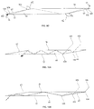
- FIG. 1 illustrates a sectional view of a prior art light-guide optical element.
- the first reflecting surface 16 is illuminated by a plane light wave 18 emanating from a display source 4 and collimated by a lens 6 , located behind the device.
- the reflecting surface 16 reflects the incident light from the source, such that the light is trapped inside a planar substrate 20 by total internal reflection. After several reflections off the major surfaces 26 , 27 of the substrate, the trapped light waves reach an array of partially reflecting surfaces 22 , which couple the light out of the substrate into an eye 24 , having a pupil 25 , of a viewer.
- the angle ⁇ sur2 between the reflecting surfaces and the major surfaces of the substrate is:
- the trapped rays arrive at the reflecting surfaces from two distinct directions 28 , 30 .
- the trapped rays arrive at the partially reflecting surface 22 from one of these directions 28 after an even number of reflections from the substrate major surfaces 26 and 27 , wherein the incident angle ⁇ ref between the trapped ray and the normal to the reflecting surface is:
- the minus sign denotes that the trapped ray impinges on the other side of the partially reflecting surface 22 .
- each ray first arrives at the surface from the direction 30 , wherein some of the rays again impinge on the surface from direction 28 .
- the ray then intersects the same partially reflecting surface at point 34 at an incident angle of 75°,without a noticeable reflection, and then intersects again at point 36 with an incident angle of 25°,where another portion of the energy of the ray is coupled out of the substrate.
- the ray 38 shown in FIG. 2B undergoes only one reflection 40 from the same surface. Further multiple reflections occur at other partially reflecting surfaces.
- FIG. 3 illustrates this non-uniformity phenomenon with a detailed sectional view of the partially reflective surface 22 , which couples light trapped inside the substrate out and into the eye 24 of a viewer.
- the ray 31 is reflected off the upper surface 27 , next to the line 50 , which is the intersection of the reflecting surface 22 with the upper surface 27 . Since this ray does not impinge on the reflecting surface 22 , its brightness remains the same and its first incidence at surface 22 is at the point 52 , after double reflection from both external surfaces. At this point, the light wave is partially reflected and the ray 54 is coupled out of the substrate.
- the first incidence at surface 22 is at point 56 , before it meets the upper surface 27 , wherein the light wave is partially reflected and the ray 58 is coupled out of the substrate.
- the brightness of the coupled-out ray is lower than the adjacent ray 54 .
- all the coupled-out light rays with the same coupled-in angle as 31 that arrive at surface 22 left of the point 52 have a lower brightness. Consequently, the reflectance from surface 22 is actually “darker” left of the point 52 for this particular couple-in angle.
- the human eye tolerates significant variations in brightness, which remains unnoticed.
- the eye integrates the light which emerges from a single viewing angle and focuses it onto one point on the retina, and since the response curve of the eye is logarithmic, small variations, if any, in the brightness of the display will not be noticeable. Therefore, even for moderate levels of illumination uniformity within the display, the human eye experiences a high-quality image. The required moderate uniformity can readily be achieved with the element illustrated in FIG. 1 .
- a comparatively large number of partially reflecting surfaces is needed to achieve the desired output aperture.
- the “darker” portions of the partially reflecting surfaces 22 contribute less to the coupling of the trapped light waves out of the substrate, their impact on the optical performance of the substrate can be only negative, namely, there will be darker portions in the output aperture of the system and dark stripes will exist in the image.
- the transparency of each one of the reflecting surfaces is, however, uniform with respect to the light waves from the external scene. Therefore, if overlapping is set between the partially reflective surfaces to compensate for the darker portions in the output aperture, then rays from the output scene that cross these overlapped areas will suffer from double attenuations and darker stripes will be created in the external scene. This phenomenon significantly reduces the performance not only of displays which are located at a distance from the eye, such as head-up displays, but also that of near-eye displays, and hence, it cannot be utilized.
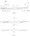
- FIGS. 4A and 4B illustrate embodiments for overcoming the above-described problem, according to the present invention. Instead of partially overcoming the undesired secondary reflections from the partially reflecting surfaces, these reflections are utilized to expand the output aperture of the optical system.
- two rays 63 from a plane light waves emanating from a display source and collimated by a lens (not shown) enter a light transparent substrate 64 , having two parallel major surfaces 70 and 72 , at an incident angle of ⁇ in (0) in respect to axis 61 , which is normal to the major surfaces 70 , 72 of the substrate.
- the rays impinge on the reflecting surface 65 which is inclined at an angle ⁇ sur1 to the major surfaces of the substrate.
- the reflecting surface 65 reflects the incident light rays such that the light rays are trapped inside a planar substrate 64 by total internal reflection from the major surfaces.
- the trapped light rays reach a second flat reflecting surface 67 , which couples the light rays out of the substrate.
- the coupled-out light rays are inclined to the substrate at the same angle as the incident light rays.
- the coupled-in light waves behave similar to the light waves illustrated in the prior art of FIG. 1 .
- FIG. 4B illustrates, a different behavior wherein two light rays 68 , having the same incident angle of ⁇ in (0) as rays 63 , impinge on points 69 which are located at the right side of the reflecting surface 65 .
- the coupled light rays are trapped inside the substrate at an off-axis angle of ⁇ in (1)
- the light rays are reflected from the upper major surface 70 , and impinge again on points 71 at surface 65 .
- the trapped light rays reach the second reflecting surface 67 .
- the light rays 68 first impinge on points 74 which are located at the right side (which is practically an active side) of the reflecting surface 67 .
- the light rays are reflected from the lower major surface 72 and impinge again on points 76 located at the right side of the reflecting surface 67 .
- the light rays 68 which are reflected twice from the coupling-in reflecting surface 65 , as well as from the active side of the coupling-out surface 67 , are coupled out from the substrate at the same off-axis angle ⁇ out as the other two rays 63 which are reflected only once from surfaced 65 and 67 , which is also the same incident input angle of these four rays on the substrate major planes.
- the optical element 64 of the present invention is differentiated from the prior art element 20 illustrated in FIGS. 1-3 by some prominent characteristics: first of all, different rays emanating from the same input light waves (such as rays 63 and 68 in FIGS. 4A and 4B ) propagate inside the substrate having different off-axis angles ( ⁇ in (1) and ⁇ in (2) , respectively). In addition, some of the trapped light rays impinge on the same side of the coupling-out reflecting surface with two different incident angles and have to be reflected at least twice from this surface in order to be coupled out from the substrate. As a result, proper notation rules must be defined in order to correctly note the various parameters of the trapped light rays inside the substrate.
- ⁇ in ( i ) ⁇ ( cen ) ⁇ in ( i ) ⁇ ( max ) + ⁇ in ( i ) ⁇ ( min ) 2 , ( 11 )
- the FOV inside the substrate does not depend on the order (i).
- the inclination of the image can be adjusted by adding a partially reflecting surface 79 which is inclined at an angle of
- the interface plane 83 ( FIG. 5D ) between the substrate 64 and the prism 80 .
- the first order image F (1) should be reflected from that plane, while the zero order image F (0) should substantially pass through it, after being reflected from surface 67 , with no significant reflections.
- the optical wave pass again through the interface plane 83 and here also it is required that the undesired reflections will be minimized.
- a possible way to achieve it this, as illustrated in FIG. 5D is to use an air gap in the interface plane 83 .
- optical adhesive in the interface plane 83 , in order to cement the prism 80 with the substrate 64 .
- the light waves are s-polarized.
- the critical angle is therefore ⁇ cr >45.4°. All the optical rays in the higher orders F (1) and F (2) have off-axis angles higher than the critical angle, and therefore, they are totally reflected from the interface plane 83 . All the optical rays in the zero order impinge on the interface plane at an incident angle lower than the critical angle, and hence, they pass through it. To minimize the Fresnel reflections of the coupled-out light waves from the interface plane, however, it is preferred to apply a suitable anti-reflective (AR) coating to this plane.
- AR anti-reflective
- FIG. 6 illustrates the graph of the reflection from the interface plane coated with an appropriate AR coating as a function of the incident angle for three different wavelengths: 450 nm, 550 nm and 650 nm, which practically cover the relevant photopic region.
- the reflection is 100% for the angular spectrum above 45°,while it is below 3% for the incident angles ⁇ 30°,40° ⁇ of the zero order, as well as for the light waves which pass again substantially normal to the plane 83 after being reflected from surface 79 .
- surface 67 will be reflective for the incident angles of the higher orders ⁇ so (1) and ⁇ so (2) , as well as transparent for the coupled-out light waves which pass through this plane after being coupled out from the substrate, reflected by surface 79 , and pass again through the interface plane 83 . That is, for the exemplified system given above, the surface should be reflective for incident angles above 40° and substantially transparent for incident angles below 15°.
- an air gap between surface 67 and prism 82 is a possible solution, but here again it is preferred to cement the element together with an optical adhesive.
- the requirements from the dielectric coating that should be applied to the surface 67 is therefore to be reflective for the incident angles of 40° ⁇ so (1) ⁇ 45° (above 45° the light rays are totally reflected from the surface), and substantially transparent for the incident angles below 15°.
- FIG. 7 illustrates the graph of the reflection from the interface plane coated with an appropriate angular sensitive coating as a function of the incident angle for three different wavelengths: 450 nm, 550 nm and 650 nm. As shown, the reflection is higher than 93% for the angular spectrum between 40° and 45°,while it is below 2% for the incident angles below 15° as required.
- surface 79 In see-through systems, such as HMDs for military or professional applications, or for augmented reality systems, wherein the viewer should see the external scene through the substrate, surface 79 should be at least partially transparent. As a result, in such a case a partially reflecting coating should be applied to surface 79 .
- the exact ratio between the transmission and the reflection of the coating should be determined according to the various requirements of the optical system. In the event that an array of partially reflecting surfaces 79 a , 79 b . . . is used to reflect the light waves to a viewer's eye, the reflectance of the coating should be the same for all the partially reflecting surfaces in order to project a uniform image to the viewer's eye as well as to transmit a uniform external seen.
- FIG. 8A illustrates an embodiment for implementing a lens, based on the present invention.
- a collimated image 84 is coupled into the substrate 64 by the reflecting surface 65 , reflected (once or twice, depending on the order of the coupled rays) by the angular selective reflecting surface 67 , passes through the interface plane 83 , is partially reflected by the array of partially reflecting surfaces 79 a , 79 b , and passes again through surface 83 into the eye 24 of a viewer.
- the ophthalmic plano-concave lens 86 which is attached to the upper surface 70 of the substrate, focuses the images to a convenient distance, and optionally corrects other aberrations of the viewer's eye, including astigmatism. Since the lens 86 is attached to prism 82 , which is not active in the mechanism for trapping of the optical waves inside the substrate 64 by total internal reflection, a simple cementing procedure can be used to optically attach the lens 86 to prism 82 . There are applications, however, such as illustrated in FIG. 8B , where the lens 86 should have an extended aperture, and hence, it should also be attached to the upper surface 70 of the substrate.
- an isolation layer should be provided in the interface plane 85 between the lens and the substrate, to ensure the trapping of the image rays inside the substrate by a total internal reflection.
- a possible way to achieve this is to use an air gap in the interface plane 85 . It is preferred, however, as explained above, to apply an optical adhesive in the interface plane, in order to cement the prism 82 with the lens 86 . As illustrated above in relation to FIG. 6 , an appropriate AR coating can be applied to the interface plane 85 , in order to minimize the Fresnel reflections from this plane.
- FIG. 8C illustrates a system for implementing a dual lens configuration, based on the present invention.
- a collimated image 84 is coupled into the substrate 64 by the reflecting surface 65 , reflected by the angular selective reflecting surface 67 , passes through the interface plane 83 , is partially reflected by the array of partially reflecting surfaces 79 a , 79 b . . . and passes again through surface 83 into the eye 24 of a viewer.
- Another scene image 90 from a close distance is collimated to infinity by a lens 89 , and then passed through the substrate 64 into the eye.
- the lens 86 focuses the images 84 and 90 to a convenient distance, usually the original distance of the external scene 90 , and corrects other aberrations of the viewer's eye, if required. Since the lower surface 81 of prism 80 is not active with regard to the optical waves that are coupled inside the substrate 64 by total internal reflection and directed by the reflecting surface 79 into the viewer's eye, it is possible to optically attach a prism 80 with a lens 89 using a conventional cementing procedure.
- the lenses 86 and 89 plotted in FIGS. 8A-8C are simple plano-concave and plano-convex lenses, respectively.
- Fresnel lenses which can be made of thin molded plastic plates with fine steps.
- an alternative way for realizing the lenses 86 or 89 instead of as fixed lenses as described above, is to use electronically controlled dynamic lenses.
- a high resolution, spatial light modulator (SLM) can be used to form a dynamic focusing element.
- the most popular sources for that purpose are LCD devices, but other dynamic SLM devices can be used as well.
- High resolution, dynamic lenses having several hundred lines/mm are known.
- This kind of electro-optically controlled lenses can be used as the desired dynamic elements in the present invention, instead of the fixed lenses described above in conjunction with FIGS. 8A-8C . Therefore, the operator can determine and set, in real time, the exact focal planes of both the virtual image projected by the substrate 64 as well as the real image of the external view.
- FIGS. 4-8 has several significant advantages as compared to the embodiment of the prior art illustrated in FIGS. 1-3 .
- the main reason for this is that because of the small angle of ⁇ sur2 , the active area of the output aperture of the substrate having a single reflecting surface 67 , is much larger than that of a substrate having a single coupling-out partially reflecting surface which is based on the prior art technology.
- the fabrication process of the substrate will be much simpler than that of the prior art.
- the projected image can be much smoother and with higher optical quality than that of the multi-facet element of the prior art.
- a ghost image problem might be accrued at the edge of the reflecting surface 67 .
- a ray 91 having an off-axis angle ⁇ in (0) is traced from the output aperture backward to the input aperture of the substrate 64 .
- the ray 91 impinges on the reflecting surface at point 93 a and is reflected not only twice, but rather three times from the reflecting surface 67 .
- the ray is trapped inside the substrate 64 having an off-axis angle ⁇ in (3) , which is located in the third order of the coupled-in light waves.
- this angle fulfils the relation ⁇ in (3) >90° ⁇ sur2 , and as a result, it is not a “legal” angle.
- this angle in not necessarily the required angle ⁇ in (0) .
- FIG. 9B A possible way to overcome this problem is illustrated in FIG. 9B .
- a flat transparent plate 95 is cemented to the lower surface 72 of the substrate 64 defining an interface plane 96 .
- the ray 91 is reflected now only twice from surface 67 before being coupled into the substrate 64 . Therefore, the coupled ray 97 propagates inside the substrate having an off-axis angle ⁇ in (2) which is a “legal” direction, and no ghost image is created in the image.
- FIG. 9C An alternative manner of overcoming the ghost image problem is illustrated in FIG. 9C .
- the reflecting surface 79 is shifted inside the prism 80 such that it does not cover the entire aperture of the reflecting surface 67 . That is to say, the rays that are reflected at the far edge by segment 99 of the reflecting surface 67 are not reflected back to the viewer's eye by surface 79 . As a result, part of surface 67 is practically blocked from being active and the segment 99 becomes non-active. Therefore, the ray 91 having the “wrong” direction does not illuminates the viewer's eye and the ghost image is avoided.
- the thickness of plate 95 or the shift of surface 79 can be determined according to the various parameters of the optical system such as the required measure of the output aperture, the FOV of the system and the desired overall thickness of the substrate.
- FIG. 9D Another alternative for overcoming the ghost image problem is illustrated in FIG. 9D .
- the coupled ray 91 impinges on the lower major surface 72 before impinging on the reflecting surface 65 having an off-axis angle ⁇ in (3) , namely, the same off-axis angle it has while reflected from surface 67 at the third point 93 c .
- the coupled ray 91 is reflected three times from surface 65 at points 93 d , 93 e and 93 f before being coupled out from the substrate having the off-axis angle ⁇ in (1) , which is the “proper” angle.
- the various parameters of the optical system such as the inclination angle of the reflecting surfaces 65 and 67 and the thickness, the length and the refractive index of the substrate, it is possible to design the system such that for most of the relevant optical rays the triple reflection from surface 67 will be compensated by a triple reflection from surface 65 so that the ghost images and the gaps in the image will be avoided.
- the points on the boundary line 100 between the edge of the reflective surface 65 and the lower surface 72 of the substrate 64 should be illuminated for a single light wave by two different rays that enter the substrate in two different locations: a ray 101 (dotted line) that illuminates directly surface 65 at the boundary line 100 , and another ray 102 (dashed line) which is first reflected by the reflecting surface 65 at point 103 and then by the upper surface 70 of the substrate 64 before illuminating the lower surface 72 just left to the boundary line.
- the two rays 101 and 102 from the same point in the display source, which are propagated at the first order inside the substrate, are coupled into the substrate 64 remotely located from each other: 101 at the left edge and 102 approximately at the center of surface 65 , respectively.
- the rays are, however, coupled out by the coupling-out element 67 located adjacent to each other at the right part of surface 67 . Therefore, the entire area of surface 65 between points 103 and 100 should be illuminated by the light wave were the rays 101 and 102 originated from. Consequently, this area should be entirely illuminated by all the light waves that are coupled into the substrate.
- the points on the boundary line 100 between the edge of the reflective surface 65 and the lower surface 72 should be illuminated for the same single light wave that illustrated above in FIG. 10A , by two other different rays that enter the substrate in two different locations: a ray 105 (dashed-dotted line) that illuminates surface 65 at the boundary line 100 after one reflection from surface 65 at a point located just right to 103 and one reflection from surface 70 , and another ray 106 (solid line) which is reflected twice by the reflecting surface 65 and twice by the upper surface 70 of the substrate 64 before illuminating the lower surface 72 just left to the boundary line.
- a ray 105 dashex-dotted line
- another ray 106 solid line
- the two rays 105 and 106 from the same point in the display source, which are propagating at the second order inside the substrate, are coupled into the substrate 64 remotely located from each other: 105 approximately at the center and 106 close to the right edge of surface 65 , respectively. They are, however, coupled out by the coupling-out element 67 located adjacent to each other at the left part of surface 67 . Therefore, the entire area of surface 65 between points 103 and the right edge 104 of surface 65 should be illuminated by the light wave, where the rays 105 and 106 originated from. Consequently, this area should be entirely illuminated by all the light waves that are coupled into the substrate.
- FIGS. 10A and 10B There are two conclusions from FIGS. 10A and 10B :
- the entire area of surface 65 should be illuminated by light waves that are coupled into the substrate, and;
- the first order of the coupled light waves illuminates the left part of surface 65 and is coupled out at the right part of surface 67
- the second order of the coupled light waves illuminates the right part of surface 65 and is coupled out at the left part of surface 67 .
- the aperture of the coupling-in surface 65 is similar to that of the coupling-out surface 67 .
- a large output aperture is required.
- an appropriate method should be found to reduce the input aperture for a given output aperture, or alternatively, to increase the output aperture for a given input aperture.
- FIGS. 11A-11D An embodiment for increasing the output aperture for a given input aperture is illustrated in FIGS. 11A-11D .
- an optical ray 107 having an input direction of ⁇ in (0) impinges on an optical element 109 composed of two substrates 110 a and 110 b , wherein the lower surface 111 a of substrate 110 a is attached to the upper surface 112 b of substrate 110 b defining an interface plane 117 .
- the coupling-in element 114 a of the upper substrate 110 a is not a simple reflecting surface as surface 65 in substrate 64 , but a partially reflecting surface, meaning that the input ray 107 is split into two rays (preferably having the same brightness) 107 a and 107 b which are reflected from surfaces 114 a and 114 b and coupled inside substrates 110 a and 110 b , respectively by total internal reflection.
- surface 114 b can be a simple reflecting surface. As shown, rays 107 a and 107 b are reflected once from the left parts of surfaces 114 a and 114 b , respectively, and propagated inside the substrates in the first order having an angle of ⁇ in (1) .
- FIG. 11B illustrates the same embodiment where now the input ray 107 impinges on the right side of surfaces 114 a and 114 b .
- rays 107 a and 107 b are reflected twice from surfaces 114 a and 114 b , respectively, and propagated inside the substrates in the second order having an angle of ⁇ in (2) . Consequently, they are coupled out from the substrate by a double reflection from the left parts of the coupling-out surfaces 116 a and 116 b having an output angle of ⁇ in (0) .
- surface 114 a which is practically the input aperture of the optical device 109 , has approximately half the size of the output aperture, which is practically the combination of the coupling-out surfaces 116 a and 116 b together.
- the interface plane 117 between the substrates 110 a and 110 b There are two contradicting requirements from the interface plane 117 between the substrates 110 a and 110 b .
- the first two orders image F (1) and F (2) should be reflected from that plane, while the zero order image F (0) from the upper substrate 110 a should substantially pass through it, after being reflected from surface 116 a , with no significant reflections.
- surface 117 should be transparent to ray 107 b that passes through surface 114 a having the input angle of ⁇ in (0) .
- the transparency of optical device 109 for substantially normal incident light should be as high as possible. A possible way to achieve this is to use an air gap in the interface plane 117 .
- An alternative manner for achieving this while maintaining the rigidness of the device is to cement substrates 110 a and 110 b together using the same cementing method which utilizes low-index adhesive, as illustrated hereinabove in relation to the interface plane 83 in FIG. 5D .
- the two substrates 110 a and 110 b are similar to each other, i.e., the inclination angles ⁇ sur1 of the coupling-in devices 114 a and 114 b , as well as the inclination angles ⁇ sur2 of the coupling-out devices 116 a and 116 b , are the same.
- the two substrates have the same thickness. It is possible, however, to attach two substrates having two different characteristics.
- the upper substrate 110 a has the same parameters as the system illustrated above in relation to Eq. (23).
- the light waves are s-polarized.
- the critical angle is therefore ⁇ cr >45.4°.
- All the light waves propagating in the first order and having the combined FOV of F (1) ⁇ 46°,60° ⁇ have off-axis angles higher than the critical angle, and therefore, they are totally reflected from the interface plane 117 between the substrates. Since the practical output aperture of each substrate directly depends on tan ⁇ sur2 , the thickness of the lower substrate 110 b should be slightly increased, in order to equalize the output apertures of the two substrates.
- the output aperture of element 109 is doubled as compared to that of the single substrate 64 in FIG.
- the left edge of surface 116 a is not active, as illustrated above in relation to FIGS. 9A-9C , it is possible to block this part by slightly shifting the lower substrate 110 b . As illustrated in FIG. 11D , the reflecting surfaces 116 a and 116 b are no longer co-linear. The left edge 118 of surface 110 a does not coincide with the right edge 120 of substrate 110 b , which is slightly shifted rightward, and hence, the inactive part 122 of surface 110 a is practically blocked.
- FIGS. 12A-12B Still an alternative embodiment to practically decrease the input aperture of the optical device is illustrated in FIGS. 12A-12B .
- an angular sensitive partially reflecting surface 124 is embedded inside the substrate 64 .
- a ray 127 impinges on the left part 125 of surface 65 is coupled into the substrate 64 after one reflection from surface 65 , and hence, propagates inside the substrate 64 having the first order off-axis angle of ⁇ in (1) .
- the ray 127 impinges on surface 124 at point 128 a . Since the ray impinges on the surface from the left side, it behaves similarly to the rays that impinge on surface 67 , and hence, Eq. (16) should be used to calculate to incident angle of ray 127 at point 128 a .
- ⁇ sp (128a) ⁇ in (1) ⁇ spr . (33)
- ray 130 propagates inside the substrate 64 having the second order off-axis angle of ⁇ in (2) .
- ray 129 passes through surface 124 without any significant reflectance and continues to propagate inside the substrate having the first order off-axis angle. Consequently, if the entire left part 125 of surface 65 is illuminated by all the light waves coupled into the substrate, the substrate 64 , as explained above in relation to FIG. 10A , will be filled by the first order of the coupled light waves. After being split by surface 124 , part of the light will continue to fill the substrate by the first order, while the part of the light which is reflected by surface 124 will now fill the second order of the coupled light waves.
- substantially the entire aperture of the coupling-out surface 67 will be illuminated by the first and the second orders of the coupled waves and the output light waves will be coupled-out from substantially the entire active aperture of surface 67 .
- the output aperture remains the entire active aperture of surface 67
- the input aperture of the substrate is practically reduced by a half.
- the penalty is that the brightness of the coupled-out light waves is also reduced by a half.
- FIG. 12B A similar embodiment for reducing the input aperture by a half is illustrated in FIG. 12B .
- a ray 132 impinges on the right part 134 of surface 65 , is coupled into the substrate 64 after two reflections from surface 65 , and hence, propagates inside the substrate 64 having the second order off-axis angle of ⁇ in (2) ).
- the ray 132 impinges on surface 124 at the point 135 a . Since the ray impinges on the surface from the left side it behaves similarly to the rays that impinges on surface 67 , and hence, Eq. (16) should be used to calculate to incident angle of ray 132 at point 135 a .
- ⁇ sp (135a) ⁇ in (2)
- ⁇ spr ⁇ in (1) + ⁇ spr .
- ray 137 propagates inside the substrate 64 having the first order off-axis angle of ⁇ in (1) ). After one reflection from the lower major surface 72 of the substrate 64 , the ray 137 impinges on surface 124 at the point 135 b . Since the ray impinges on the surface from the left side, it behaves similarly to the rays that impinge on surface 67 , and hence, Eq. (16) should be used to calculate to incident angle of ray 127 at point 128 c .
- ⁇ sp (135b) ⁇ in (1) ⁇ spr , (39) the condition of Eq. (29) is fulfilled, ray 137 passes through surface 124 without any significant reflectance, and it continues to propagate inside the substrate having the first order off-axis angle.
- FIG. 12B The practical function of the embodiment illustrated in FIG. 12B is similar to that illustrated in FIG. 12A . Only half of the input aperture 65 is illuminated by the input light waves, while the output light waves are coupled out from the entire aperture of the coupling-out surface 67 . The difference is that while in FIG. 12A only the left part 125 of surface 65 is illuminated by the input light waves, in FIG. 12B the right part 134 of surface 65 is used, but the outcome is similar, and the entire output surface is exploited. Usually, the decision as to which part of surface 65 to actually use, depends on the various parameters of the optical system.
- FIGS. 12A-12B wherein as angular selective reflecting surfaces is embedded inside the substrate 64 , can be exploited for other usages, not necessarily for reducing the input aperture.
- An issue that should be considered is the uniformity of the input light waves that illuminate the input aperture 65 . Assuming, for instance, that the brightness of ray 101 in FIG. 10A is lower than that of ray 102 , as a result of a non-perfect imaging system, this non similarity will hardly be seen by a direct viewing of the input plane wave, because of the remoteness between the rays. After being coupled into the substrate 64 , however, this condition changes and the two rays 101 and 102 propagate inside the substrate 64 adjacent to each other.
- the two rays that are reflected from surface 67 and are coupled out from the substrate have different brightness. Unlike the input light wave, however, the two rays are now adjacent to each other and this dissimilarity will be easily seen as a dark line in the coupled-out image. The same problem occurs if the brightness of ray 106 in FIG. 10B is lower than that of ray 105 , or vice versa.
- FIG. 12C illustrates an embodiment which overcomes this non-uniformity problem.
- the same angular sensitive partially reflecting surface 124 is embedded inside the substrate 64 , but now the entire input aperture 65 is illuminated by the input light waves.
- two different rays, 127 which illuminates the left part 125 close to the center of surface 65 , and 132 which illuminates the far edge of the right part 134 (and consequently, have lower brightness than ray 127 ) are propagated inside the substrate 64 having the first and the second order off-axis angles, respectively.
- the two rays coincide at point 138 on surface 124 and as explained above in relation to FIGS. 12A and 12B , both of them will be partially reflected by the surface 124 and partially pass through it.
- ray 139 which propagates inside the substrate having a first order off-axis angle, will be a mixture of the part of ray 127 which passes through surface 124 , and the part of ray 132 which is reflected by the surface.
- ray 140 which propagates inside the substrate having a second order off-axis angle, will be a mixture of the part of ray 132 which passes through surface 124 and the part of ray 127 which is reflected by the surface.
- Rays 139 and 140 are thus mixtures of the original rays 127 and 132 , but unlike the original rays, the two rays 139 and 140 which are originated from surface 124 now have a similar brightness.
- the two major surfaces of the substrate 64 should be strictly parallel to each other, since any deviation between the incident angles of the trapped light rays on the two major surfaces will cause, at each reflecting cycle, a drift in the off-axis angle ⁇ in (i) , and since the trapped light rays from the higher order undergo a much smaller number of reflections from the major surfaces of the substrate than those from the lower order, the drift of the low order will be much more noticeable than that of the high order.
- the ratio between the length and the thickness of the substrate can be high, and hence, the number of reflections from the major surfaces of the lower order can be very, and therefore the required parallelism cannot be achieve by conventional fabrication methods.
- FIG. 12D A possible approach for overcoming the above problem is illustrated in FIG. 12D .
- An angular sensitive reflecting surface 141 which is parallel to surfaces 65 and 67 , is embedded inside the substrate 64 , but here the reflecting characteristics of this surface are different than that of surface 124 in FIGS. 12A-12C .
- surface 141 is now substantially reflective.
- surface 141 will be substantially transparent for the coupled light rays 127 and 132 impinging thereon at points 142 and 144 , respectively, having a first order off-axis angle and impinge on the right side of the surfaces.
- surface 141 will be substantially reflective.
- rays 127 and 132 will be reflected from surface 141 having a second and a first order off-axis angle, respectively, namely, rays 127 and 132 exchange their off-axis angles at the coinciding point 146 . Therefore, assuming that surface 141 is located at the center of substrate 64 , evenly positioned between surfaces 65 and 67 , rays 127 and 132 undergo a similar number of reflections from the major surfaces of the substrate 64 . Assuming that the entire aperture of surface 65 is illuminated by the input light waves, for each input light wave all the coupled rays will have substantially the same number of reflections from the major surfaces of the substrate 64 , and the parallelism issue will thus be considerably improved.
- the light waves are s-polarized.
- FIG. 13 illustrates the graph of the reflection from the reflective surface 124 coated with an appropriate angular sensitive dielectric coating as a function of the incident angle for three different wavelengths: 450 nm, 550 nm and 650 nm. As shown, the reflection is approximately 50% for the angular spectrum between 57° and 67°,while it is very low for the incident angles ⁇ 33°,43° ⁇ of the zero order.
- FIG. 14 illustrates the graph of the reflection from the reflective surface 141 coated with an appropriate angular sensitive dielectric coating as a function of the incident angle for three different wavelengths: 450 nm, 550 nm and 650 nm. As shown, the reflection is 100% for the angular spectrum above 57°,while it is practically zero for the incident angles ⁇ 33°,43° ⁇ of the zero order.
- the coupling-in element is a slanted reflecting surface.
- the reason for this is the necessity to couple the first, as well as the second, order of the light waves inside the substrate.
- FIGS. 12A-12B where only the first or the second order is, respectively, coupled into the substrate by the coupling-in element, other optical means can be utilized.
- a prism 148 is optically attached to the upper major surface 70 of the substrate 64 .
- the left ray 149 illuminates the upper major surface 70 just right to edge 153 of the prism
- the right ray 150 passes through surface 70 , is totally reflected from the lower surface 72 , and then impinges on the upper surface 72 just left to the edge 153 .
- the two rays 149 and 150 are coupled inside the substrate 64 , having the first order off-axis angle of ⁇ in (1) , while propagating inside the substrate 64 adjacent to each other.
- the reflected rays 158 and 160 propagate inside the substrate 20 adjacent to each other having the second order off-axis angle of ⁇ in (2) . Consequently, all the rays of the same input light waves covering the input aperture 152 , will fill the substrate by the first order light waves, and after being partially reflected from surface 124 , will also fill the substrate by the second order light waves. As a result, the output light waves are coupled out from the substrate by the entire active aperture of surface 67 .
- the coupling-in element is a prism 162 which is optically attached to a slanted edge 163 of the substrate. As illustrated, in the embodiments of FIGS.
- the input aperture is significantly smaller than that of the embodiments illustrated in FIGS. 4-11 .
- realizing modified embodiments wherein light waves having the second order off-axis angles are directly coupled into the substrate utilizing coupling-in prisms similar to those illustrated in FIGS. 15A and 15B is also possible. In that case light waves having the first order off-axis angles will be created inside the substrate in a method similar to that illustrated in FIG. 12B .
- FIGS. 12A-12C Another issue that should be considered is the uniformity of the light waves that are split by surface 124 in the embodiments of FIGS. 12A-12C .
- the trapped rays having the first order off-axis angle of ⁇ in (1) are partially reflected only once from the left side of surface 124 .
- FIG. 16A there are rays, however, which are partially reflected twice from surface 124 .
- ray 164 is first partially reflected from surface 124 at point 165 , located in proximity to the intersection between surface 124 and the upper major surface 70 .
- the part of ray 164 which passes through surface 124 at point 165 is reflected from the lower major surface 72 , passes through surface 124 , is reflected from the upper surface 70 and then is partially reflected again from surface 124 at point 166 . Since the brightness of this part of the ray has been already reduced by a half, while splitting at point 165 , the brightness of the split rays from point 166 will be approximately 25% of that of the original ray 164 , namely, ray 164 has been split into three different rays: ray 164 a which is reflected from surface 124 at point 165 and has about a half of the brightness of the original ray 164 , and rays 164 b and 164 c , which pass through surface 164 at point 165 and then pass again, or are reflected, respectively, by surface 164 at point 166 , which rays have about a quarter of the brightness of the original ray 164 .
- the unevenness is caused by a non-uniformity of the different rays of a single light wave, which is associated with a single pixel in the image, meaning that different rays belonging to the same plane light wave, and consequently having the same direction, have different intensities. Therefore, the unevenness of this plane wave can be solved if the various rays of this uneven wave will be mixed together.
- a proper mixing arrangement should be advantageously be added to the substrate 64 , in order to improve the uniformity of the plane waves, which are trapped inside the substrate by total internal reflection.
- this unevenness problem may be solved by attaching a flat transparent plate 167 to one of the major surfaces 72 of the substrate 64 , wherein a beam-splitting arrangement is applied to the interface plane 168 between the substrate 64 and the transparent plate 167 .
- a beam-splitting arrangement is applied to the interface plane 168 between the substrate 64 and the transparent plate 167 .
- two light rays, 164 and 169 having different intensities intersect each other at point 170 located at the interface plane 168 .
- Ray 164 which is illustrated above in FIG. 16A , has already been partially reflected by surface 124 , and hence, has a lower brightness then the original ray.
- the other ray 169 which passes through the interface plane at point 171 and is reflected by the lower surface 172 of the plate 167 , did not yet pass through surface 124 , and hence, it has a higher intensity.
- each one of the two intersecting rays is partially reflected and partially passes through the interface plane. Consequently, the two rays interchange energies between themselves, and the emerging ray 164 d from the intersection point 170 has an intensity which is closer to the average intensity of the two incident rays 164 and 169 .
- the most efficient beam-splitting arrangement is to apply a partially reflecting coating to the interface plane, wherein half of the incoming light wave is transmitted and half is reflected from the surface.
- the intensities of the emerging ray 164 d are substantially the average intensity of the two incident rays 164 and 169 , and the mixing between the rays is optimal.
- the main drawback of the coating method is that in order to avoid aberrations and smearing of the image, the direction of the trapped rays inside the substrate should be strictly retained. Therefore, a high degree of parallelism should be maintained for the three reflecting surfaces: the upper surface 70 of the substrate 64 , the lower surface 172 of the plate 167 and the interface plane 168 .
- the external surfaces of the substrate 64 and the plate 167 should have high parallelism and very good optical quality before attaching them together. Applying an optical coating to one of these external surfaces, however, will require a coating process which usually deforms the surfaces of the coated plate, especially if this plate is particularly thin. Another problem is that the light rays which are reflected from surface 67 intersect with the interface plane 168 before being coupled out from the substrate 64 . As a result, a simple reflecting coating cannot easily be applied to the interface plane 168 , since this plane should also be transparent to the light-waves that exit the substrate 64 , as well as transparent to the light wave from the external scene for see-through applications.
- the light-waves should pass through plane 168 without substantial reflections at small incident angles, and should be partially reflected at higher incident angles. This requirement complicates the coating procedure and increases the probability that the coated plate will be deformed during the coating process. Consequently, since even a minor deformation will deteriorate the performance of the imaging system, an alternative mixing arrangement should be applied.
- FIG. 16C An alternative embodiment is illustrated in FIG. 16C .
- the substrate 64 and the plate 167 are optically cemented using an optical adhesive 176 having a refractive index, which is substantially different than the refractive index of the light transmitting substrate 64 and the flat plate 167 .
- the Fresnel reflections from plane 168 will be significant and the light waves which are coupled inside the substrate, will be partially reflected from the interface plane.
- the incident rays are reflected twice from the interface plane 168 , once from the interface plane between the substrate 64 and the adhesive 176 , and the second time from the interface plane between the optical adhesive 176 and the transparent plate 167 .
- three different rays 164 , 169 and 178 are trapped inside the substrate.
- the two rays 169 and 178 intersect each other at point 171 which is located at the interface plane 168 .
- each one of the two intersecting rays is partially reflected and partially passes through the interface plane.
- the two rays interchange energies between themselves and the emerging rays 179 and 180 from the intersection point 171 have intensities which are closer to the average intensity of the two incident rays 169 and 178 .
- the two rays 164 and 179 intersect each other at point 170 , interchange energies between themselves and the emerging rays 181 and 182 from the intersection point 170 have intensities which are closer to the average intensity of the two incident rays 164 and 179 . Therefore, the three rays 164 , 179 and 178 , interchange energies during this process and their intensities are now closer to the average intensity.
- Rays 164 and 178 do not interchange energies directly, but indirectly through the two separate interactions with ray 179 , at points 170 and 171 .
- the optimal mixing will be achieved if the Fresnel reflections from the interface plane 168 are close to 50%. Since, however, Fresnel reflections are very sensitive to the incident angle, it is impossible to find an optical adhesive having a refractive index that yields Fresnel reflection of 50% for the entire FOV of the coupled image, and since the trapped rays intersect not only once, but rather a few times with the interface plane, it is possible to find a mixing arrangement that will be acceptable even for Fresnel reflections which are very different than the optimal value of 50%.
- the reflection is 100% for the angular spectrum above 53° as a result of total internal reflection, and hence, no mixing effect is achieved for these angles.
- the entire second order FOV F (2) ⁇ 69°,79° ⁇ , all the light waves are totally internally reflected from the interface plane 168 and no mixing effect is achieved for the entire order.
- the non-uniformity problem is substantially negligible for the rays having these angles.
- the reflection is between 20% and 80%, and a good mixing effect can be achieved.
- the device illustrated here is not limited to utilization of a single flat plate. Two or more flat plates, having various thicknesses and refractive indices, can be optically attached to one or both of the major surfaces using various optical adhesives. In any case, the exact parameters of the transparent plates and the adhesives can be used according to the various requirements of the systems.
- FIGS. 18A-18C illustrate a modified version of device 109 , wherein the input beamsplitter 183 is sensitive to the incident angle of the input light waves and, as a result the efficiency of the optical system, is significantly improved and the brightness of the coupled-out image is substantially retained similar to that of the input image.
- the fact that the light waves which are coupled out from the substrate do not have to illuminate the entire active area of the coupling-out surface, as was done in the embodiments of FIGS. 11A-11D was utilized.
- the two marginal and the central light waves of the image are coupled out from the substrate and re-directed into the viewer's eye 24 .
- the light waves 107 R, 107 M, and 107 L having the zero order off-axis angles ⁇ in (0) (max), ⁇ in (0) (mid) and ⁇ in (0) (min), illuminate only the parts 67 R, 67 M and 67 L of the coupling-out reflecting surface 67 , respectively, and are reflected by surface 79 into to EMB 197 .
- the coupled-in light waves are split in such a way that they will illuminate only the required respective part of surface 67 , and the original brightness will be preserved.
- the angular range of the light waves F sur1 (0) ⁇ min , ⁇ max ⁇ which impinge on the input surface 183 ( FIG. 18A ), is divided into three substantially equal segments: F low (0) ⁇ min , ⁇ m1 ⁇ , F mid (0) ⁇ m1 , ⁇ m2 ⁇ and F max (0) ⁇ m2 , ⁇ max ⁇ .
- the aim of the embodiment is that the light waves having the higher incident angles in the FOV of F max (0) ⁇ m2 , ⁇ max ⁇ will be coupled out from the upper substrate 110 a by the both parts of the coupling-out element 190 a and 190 b ; the light waves having the lower incident angles in the FOV of F min (0) ⁇ min , ⁇ m1 ⁇ will be coupled out from the lower substrate 110 b by the both parts of the coupling-out element 190 c and 190 d , and the light waves in the FOV of F mid (0) ⁇ m1 , ⁇ m1 ⁇ will be coupled out from the upper substrate 110 a by the lower coupling-out element 190 b and from the lower substrate 110 b by the upper coupling-out element 190 c.
- surface 183 should substantially reflect all the light waves in F max (0) such that they will be coupled into the upper substrate 110 a and substantially transmit all the light waves in F min (0) , such that they will be coupled by the reflecting surface 114 into the lower substrate 110 b .
- part of the light waves in F mid (0) should be reflected by surface 183 in such a way that they will be trapped inside the upper substrate 110 a , but will be coupled out only by the lower part of the coupling-out element 190 b and part of the light waves in F mid (0) should be pass through surface 183 in such a way that they will be trapped inside the lower substrate 110 b but will be coupled out only by the upper part of the coupling-out element 190 c .
- the light waves which propagate inside the substrate having the first order off-axis angles are coupled out from the substrate by the upper part of the coupling-out element 67
- the light waves propagating inside the substrate having the second order off-axis angles are coupled out from the substrate by the lower part of the coupling-out element 67 .
- the light waves in this FOV it is necessary for the light waves in this FOV to be coupled inside the upper substrate 110 a having the second order off-axis angles, and hence, will be coupled out by the lower part 190 b , and in addition, will be coupled inside the lower substrate 110 b having the first order off-axis angles, and hence, will be coupled out by the upper part 190 c.
- the angular sensitive reflecting surface 183 should fulfill the following three characteristics for the entire photopic range:
- FIG. 18A illustrates two rays 184 a and 184 b from the same plane input wave having incident angles of ⁇ si (0) ⁇ m1 which impinge on the lower and the upper parts of surface 183 , respectively.
- condition (b) described hereinabove the rays pass through surface 183 and are coupled into the lower substrate 110 b by the reflective surface 114 having the first and the second order off-axis angles, respectively. Consequently, the rays are coupled-out from the substrate by the reflective surfaces 190 c and 190 d , respectively.
- FIG. 18B illustrates two rays 185 a and 185 b from the same plane input wave having incident angles of ⁇ si (0) > ⁇ m2 which impinge on the lower and the upper parts of surface 183 , respectively.
- condition (a) described hereinabove the rays are reflected from surface 183 and are coupled into the upper substrate 110 a having the first and the second order off-axis angles, respectively. Consequently, the rays are coupled-out from the substrate by the reflective surfaces 190 a and 190 b respectively.
- 18C illustrates two rays 186 a and 186 b from the same plane input wave having incident angles of ⁇ m1 ⁇ si (0) ⁇ m2 , which impinge on the surfaces 183 b and 183 a , respectively.
- ray 186 b is reflected from surface 183 a and is coupled into the upper substrate 110 a having the second order off-axis angle. Consequently, the ray is coupled-out from the substrate by the lower reflective surface 190 b .
- ray 186 a passes through surface 183 b and is coupled into the lower substrate 110 b by the reflective surface 114 having the first order off-axis angle. Consequently, the ray is coupled-out from the substrate by the upper reflective surfaces 190 c , as required.
- the optical adhesive used to optically attach the slices 110 aa and 110 ab will have a refractive index close to that of the slices.
- the coupling in surfaces 183 a and 183 b and the coupling-out surfaces 190 a and 190 b should be strictly co-linear, respectively.
- the interface plane 189 should be parallel to the major surfaces 111 a and 112 a of substrate 110 a.
- FIGS. 20A-20C An alternative embodiment to realize the required angular-sensitive beamsplitter is illustrated in FIGS. 20A-20C .
- the overall optical device 199 is constructed of four different substrates 191 a , 191 b , 191 c and 191 d , which are optically cemented together defining three interface planes, 193 a , 193 b and 193 c , respectively. Another difference from the embodiment of FIGS.
- the beamsplitters 183 a and 183 b are interchanged, e.g., surfaces 183 a and 183 b are cemented to the inert part 177 of element 199 using optical adhesives having proper refractive indices that now yield critical angles of ⁇ m1 and, ⁇ m2 at surfaces 183 b and 183 a , respectively.
- FIG. 20A illustrates two rays 184 a and 184 b from the same plane input wave having incident angles of ⁇ si (0) ⁇ m1 , which impinge on surface 183 b and 183 a , respectively.
- the rays pass through the surfaces and are coupled into the substrates 191 d and 191 c by the reflective surfaces 195 b and 195 a , respectively.
- the input light waves illuminate the entire areas of surfaces 195 a and 195 b , and hence, they fill the entire first and second off-axis angles and as a result illuminate the entire active areas of surfaces 190 c and 190 d which couple them out of the substrates.
- FIG. 20B illustrates two rays 185 a and 185 b from the same plane input wave having incident angles of ⁇ si (0) ⁇ m2 , which impinge on surface 183 b and 183 a , respectively.
- the rays are reflected from the surfaces and are coupled into the substrates 191 b and 191 a , respectively.
- the input light waves illuminate the entire areas of surfaces 183 a and 183 b , and hence, they fill the entire first and second off-axis angles and as a result illuminate the entire active areas of surfaces 190 a and 190 b , which couple them out of the substrates.
- FIG. 20C illustrates two rays 186 a and 186 b from the same plane input wave having incident angles of ⁇ m1 ⁇ si (0) ⁇ m2 , which impinge on the surfaces 183 b and 183 a , respectively. Since the beam-splitting mechanism was interchanged between surfaces 183 a and 183 b , ray 186 a is now reflected from surface 183 b , and is coupled into substrate 191 b and coupled out by the reflective surface 190 b . In addition, ray 186 b now passes through surface 183 a and is coupled into substrate 191 c by the reflective surface 195 a , and consequently, is coupled-out from the substrate by the reflective surface 190 c as required.
- each one of the four substrates 191 i functions independently, there are no longer any constraints on the co-linearity of each adjacent coupling-in and coupling-out surfaces as there were according to the embodiments of FIGS. 18A-18C .
- the only constraint is that for each separate substrate 191 i , the major surfaces and the coupling-in and the coupling-out surfaces should be parallel to each other, respectively.
- each separate substrate can have a different thickness and a different inclination angle according to the requirements of the optical system.
- F (0) ⁇ 36°,46 ° ⁇
- F (1) ⁇ 54°,64° ⁇
- F (2) ⁇ 72°,82° ⁇
- ⁇ sp (0) ⁇ 45°,55° ⁇
- ⁇ sp (1) ⁇ 63°,73° ⁇ , (43)
- the light waves are s-polarized.
- F (0) ⁇ 30°,46° ⁇ (which is practically a FOV of 30° in the air) and the angular range of F sur1 (0) ⁇ 39°,55° ⁇ is divided into three substantially equal segments: F low (0) ⁇ 39°,45° ⁇ , F mid (0) ⁇ 45°,50° ⁇ and F max (0) ⁇ 50°,55° ⁇ .
- FIG. 21A illustrates the graph of the reflection from the reflective surface 183 a in FIG. 18C (or surface 183 b in FIG. 20C ) coated with an appropriate AR dielectric coating as a function of the incident angle for three different wavelengths: 450 nm, 550 nm and 650 nm. As shown, the reflection is 100%, due to total internal reflection, for angular spectrum above 45.6°,while it is very low for the incident angles of ⁇ 39°,44.5° ⁇ .
- FIG. 21B illustrates the graph of the reflection from the reflective surface 183 b in FIG. 18C (or surface 183 a in FIG.
- the reflection is 100%, due to total internal reflection, for angular spectrum above 50.7°,while it is very low for the incident angles of ⁇ 39°,50° ⁇ .
- FIG. 22 illustrates the two marginal and the central light waves of the image which are coupled out from the substrate and re-directed into the viewer's eye 24 .
- the light waves 185 , 186 , and 184 having the zero order off-axis angles of ⁇ in (0) (max), ⁇ in (0) (mid) and ⁇ in (0) (min), are illuminating each only the reflection surfaces 190 a - 190 b , 190 b - 190 c and 190 c - 190 d , respectively, and are reflected by surface 79 into to EMB 197 .
- the extent of the EMB 197 is set by the two marginal rays 185 R and 184 L, which are reflected form the two edges of the overall coupling-out aperture of element 199 , and is not influenced at all by the rays 185 R and 184 L which “moved” to the center of the coupling-out aperture as a result of the new arrangement. Consequently, the EMB 197 of the embodiment which is illustrated in FIGS. 18A-18C and 20A-20C has the same large aperture as the EMB of the embodiment which is illustrated in FIGS. 11A-11C , while the output brightness is doubled.
- FIGS. 20A, 20B and 20C illustrate outlines of embodiments comprising two pairs of substrates, wherein the output aperture is increased by a factor of two without reducing the brightness of the projected image.
- the output aperture is increased by a factor of two without reducing the brightness of the projected image.
- n pairs of transparent substrates should be attached together, wherein for each pair the coupling-in, as well as the coupling-out, surfaces should be adjacently located in the same manner as, for example, surfaces 183 a and 183 b , and 190 a and 190 b ( FIG. 20A ), respectively.
- all the coupling-out surfaces should be adjacently located as surfaces 190 i in embodiment 199 .
- the angular range of the light waves which impinge on the input surface of the upper pair F sur1 ⁇ min , ⁇ max ⁇ is divided now into 2n ⁇ 1 substantially equal segments, by setting 2n ⁇ 2 equally separated angles ⁇ j .
- the coupling-in element of substrate S j should reflect all the impinging light waves having incident angles higher than the limit angle of ⁇ j ⁇ 2 , to couple these light waves inside substrate S j , and to substantially transmit all the other light waves toward the input aperture of substrate S j ⁇ 2 .
- the simplest way to achieve these requirements is to cement each respective coupling-in surface to the adjacent inert part of the embodiment, using optical adhesives having proper refractive indices that yield critical angles of ⁇ j ⁇ 2 .
- the high transparency for incident angles lower than the respective critical angles can be achieved using proper AR coatings.
- FIG. 23A illustrates an embodiment wherein the output aperture is expanded without increasing the substrate's thickness.
- an angular sensitive partially reflecting surface 198 is embedded inside the substrate 200 .
- Surface 198 is parallel to the coupling-in surface 65 and the coupling-out surface 67 .
- the surface is substantially transparent for the light waves which are coupled-out from the substrate and re-directed into the viewer's eye, as well as for the light waves from the external scene.
- a ray 202 is coupled into the substrate 200 after one reflection from surface 65 , and hence, propagated inside the substrate 200 having the first order off-axis angle of ⁇ in (1) .
- ray 202 is substantially evenly split by surface 198 , namely, approximately half of the intensity of the light ray 202 is reflected from surface 198 as ray 202 a having the off-axis angle of ⁇ in (0) ), and hence, is coupled out from the substrate 200 through the lower surface 72 .
- the other half of the intensity of the light ray 202 passes through surface 198 as ray 202 b and continue to propagate inside the substrate 200 having the same off-axis angle of ⁇ in (1) ). After one reflection from the upper major surface 70 , ray 202 b impinges again on surface 198 at point 206 b .
- ray 202 b propagates inside the substrate 200 having the second order off-axis angle of ⁇ in (2) . After two reflections from the coupling-out surface 67 , ray 202 b is coupled out from substrate 200 having the same off-axis angle ⁇ in (0) as ray 202 a.
- another ray 204 is coupled into the substrate 200 after two reflections from surface 65 , and hence, propagates inside the substrate having the second order off-axis angle of ⁇ in (2) ).
- the ray 204 After a few reflections from the major surfaces of the substrate 64 , the ray 204 impinges on surface 198 at point 207 a . Since the ray impinges on the surface from the left side and behaves similarly to the rays that impinge on surface 67 , Eq. (16) should hence be used to calculate the incident angle of ray 204 at point 207 a .
- ⁇ sp (207a) ⁇ in (2)
- ⁇ spr ⁇ in (1) + ⁇ spr .
- ray 204 propagates inside the substrate 200 having the first order off-axis angle of ⁇ in (1) ). After one reflection from the lower major surface 72 of the substrate 200 , the ray 204 impinges again on surface 198 at the point 207 b . Similarly to the behavior of ray 202 at point 206 a , ray 204 is substantially evenly split by surface 198 . Approximately half of the intensity of the light ray 204 is reflected from surface 198 as ray 204 a having the off-axis angle of ⁇ in (0) , and hence, is coupled out from the substrate 200 through the lower surface 70 .
- the other half of the intensity of the light ray 204 passes through surface 198 as ray 204 b and continues to propagate inside the substrate 200 having the same off-axis angle of ⁇ in (1) .
- ray 204 b is coupled out from substrate 200 having the same off-axis angle ⁇ in (0) as rays 202 a , 202 b and 204 a .
- the output aperture of substrate 200 is the combination of surfaces 198 and 67 . Consequently, the practical active area of the output aperture of substrate 200 has been doubled as compared to that of substrate 64 , which is illustrated in FIG. 4 , while the thickness of the substrate remains the same.
- the brightness of light waves coupled out from substrate 200 has been reduced by 50% as compared to that of substrate 64 .
- FIG. 23A illustrates an optical system 208 wherein two different substrates 210 a and 210 b are attached together. Two partially reflecting surfaces 212 a and 212 b , having the same optical characteristics as surface 198 in FIG. 23A , are embedded inside substrates 210 a and 210 b , respectively.
- An input ray 214 is split by the beam-splitting surface 216 into two parts: a ray 214 a which is coupled by surface 216 into substrate 210 a , and ray 214 b which passes through surfaces 216 and is coupled by surface 218 into substrate 210 b .
- the coupled rays 214 a and 214 b are split by surfaces 212 a and 212 b respectively.
- the rays 214 aa and 214 ba are reflected by these surfaces and coupled out from the substrate, while rays 214 ab and 214 bb pass through theses surfaces and are coupled out from the substrate by the reflecting surfaces 220 a and 220 b , respectively.
- the output aperture of the system 208 is composed of four surfaces: 212 a , 212 b , 220 a and 220 b , and the active area of this aperture is expanded accordingly.
- the coupling-out surfaces 212 b and 220 b of the lower substrate 210 b partially can block, if required, the non-active parts of surfaces 212 a and 220 a , respectively.
- the illumination, and hence, the brightness of the display sources are usually stronger at the center of the display.
- the non-uniform reflectance curve of the partially reflecting surface can compensate for the non-uniform illumination and in addition the overall brightness of the coupled-out image is improved.
- FIG. 23C An alternative embodiment 255 , wherein the output aperture is expanded without increasing the substrate's thickness and without the necessity to resort to a special partially reflecting coating as required for surface 198 , is illustrated in FIG. 23C .
- a reflecting surface 256 is embedded inside the substrate 258 .
- Surface 256 has the same reflecting characteristics as surface 67 and is parallel to the coupling-in 65 and the coupling-out 67 surfaces.
- a ray 260 is coupled into the substrate 258 after one reflection from surface 65 , and hence, propagates inside the substrate 258 having the first order off-axis angle of ⁇ in (1) .
- the ray 260 After a few reflections from the major surfaces of the substrate 258 the ray 260 impinges on surface 256 . Since the ray impinges on the surface from the right side, it behaves similarly to the rays that impinges on surface 67 , and hence, it is coupled out from the substrate 258 having an off-axis angle ⁇ in (0) and is then reflected (or partially reflected in see-through applications) into the viewer's eye similarly to what is illustrated in FIGS. 5A-5C .
- the reflected ray is, however, not propagated here undisturbed into the viewer's eye, as in the embodiments illustrated in FIGS. 5A-5C . Instead, the reflected ray impinges on a partially reflecting surface 264 a , which is parallel to surface 79 a , and is coupled inside a flat prism 267 , which is attached to the upper surface 70 of the substrate 268 in a similar way that prism 80 is attached to the lower surface 72 of the substrate.
- one way to achieve the above is to use an air gap in the interface plane 268 between the prism 267 and the substrate 258 , while another way for achieving a rigid system, is to apply an optical adhesive having a proper refractive index in the interface plane 268 , in order to cement the prism 268 with the substrate 258 .
- Part of the intensity of the light ray 260 which impinges on surface 264 a passes through the surface as ray 260 a , and continues to propagate toward the viewer's eye.
- the ray 260 b is coupled out from substrate 258 having the same off-axis angle ⁇ in (0) and is reflected from surface 79 d , which is parallel to surface 79 a , into the viewer's eye having the same direction as ray 260 a.
- another ray 262 is coupled into the substrate 258 after two reflections from surface 65 , and propagates inside the substrate having the second order off-axis angle of ⁇ in (2) .
- the ray 262 After a few reflections from the major surfaces of the substrate 258 , the ray 262 impinges on surface 256 .
- the ray impinges on the surface from the right side and behaves similarly to the rays that impinge on surface 67 , and hence, is coupled out from the substrate 258 having an off-axis angle ⁇ in (0) and is then reflected by surface 79 b (or partially reflected in see-through applications), which is parallel to surface 79 a , into the viewer's eye in a similar manner to ray 260 .
- the reflected ray impinges on the partially reflecting surface 264 b which is parallel to surface 79 b and 264 a , and is coupled inside prism 267 .
- Part of the intensity of the light ray 262 which impinges on surface 264 b , passes through the surface as ray 262 a and continues to propagate toward the viewer's eye. Since surfaces 79 b and 264 b are parallel, the other part of the intensity of the light ray 260 is reflected from surface 264 b as ray 262 b having an off-axis angle of ⁇ in (0) , and impinges again on surface 256 .
- the ray impinges on the surface from the left side and behaves similarly to the ray that impinges on surface 65 , and hence, after one reflection from surface 256 it propagates inside the substrate 258 having the first order off-axis angle of ⁇ in (1) .
- the ray 262 b is coupled out from substrate 258 having the same off-axis angle ⁇ in (0) and is reflected from surface 79 c , which is parallel to surface 79 b , into the viewer's eye having the same direction as ray 260 a .
- all of the four rays— 260 a , 260 b , 260 a and 262 b which originated from the same point on the display source, reach the viewer's eye having the same propagating direction.
- the output aperture of substrate 258 is the combination of surfaces 256 and 67 . Consequently, the practical active area of the output aperture of substrate 258 has been doubled as compared to that of substrate 64 , which is illustrated in FIG. 4 , while the thickness of the substrate remains the same.
- the brightness of light waves coupled out from substrate 258 has been reduced as compared to that of substrate 64 .
- the transmittance of the external scene for see-through applications can be achieved, since the entire element 255 is now substantially transparent to the one polarization (which is orthogonal to that of the light waves coupled inside the substrate).
- the reflecting surfaces 79 i can be totally reflective for the relevant polarization (which is the same as that of the light waves coupled inside the substrate)
- surfaces 254 i should be partially reflective for this polarization wherein the exact reflection coefficient of the surfaces can be determined according to the number of reflecting surfaces 264 i in the system.
- a reflection coefficient of 0.5 can yield a total brightness efficiency of 50% for the light waves coupled inside the substrate and transmittance of 50% for the external scene.
- the embodiment for expanding the output aperture by embedding a reflecting surface 256 in to the substrate 258 is not limited to a single reflecting surface.
- the reflectance and lateral extension of each reflecting surface 264 i should be designed to ensure the uniformity characteristics of the light waves coupled into the viewer's eye.
- the light waves are s-polarized.
- FIG. 24 illustrates the graph of the reflection from the partially reflecting surface 198 coated with an appropriate dielectric coating as a function of the incident angle for three different wavelengths: 450 nm, 550 nm and 650 nm. As shown, the reflection is 100%, due to total internal reflection, for an angular spectrum of ⁇ 60°,70° ⁇ . In addition, the reflectance curve increases from 44% at 400 to 55% at 50°,while it is very low for the incident angles below 15°,as required.
- FIGS. 5A-5D illustrate embodiments for directing the coupled-out light waves into the viewer's eye 24 where the light waves are reflected back by a reflecting surface 79 , and pass again through the substrate 64 toward the viewer's eye.
- four rays, 222 a , 222 b , 222 c and 222 d from the same light wave are coupled into the substrate 64 by the reflecting surface 65 , and then coupled out by the surface 67 having the off-axis angle ⁇ in (0) .
- the coupled-out light rays are reflected by the reflecting surface 224 , which is inclined at an angle of
- ⁇ ref 90 ⁇ ° - ⁇ in ( 0 ) ⁇ ( cen ) 2 to the lower major surface 72 of the substrate, towards the viewer's eye.
- the main drawback of this embodiment is that the longitudinal dimension (along the y-axis) of the reflecting surface 224 is big, resulting in a large and cumbersome optical system.
- FIG. 25B illustrates an alternative version of this embodiment in which an array of parallel reflecting (or alternatively partially reflecting) surfaces having the same inclination angle as surface 224 , is positioned next to the exit aperture of the substrate 64 .
- the array 225 can be embedded inside a transparent prism 226 having preferably refractive index similar to that of the substrate 64 .
- the optical system can now be much more compact than that illustrated in FIG. 25A , depending on the number of the reflecting surfaces in the array 225 and the thickness of prism 226 .
- the reflecting surfaces illustrated in FIG. 25B are adjacent to each other, i.e., the right side of each surface is adjacent to the left side of the projection of the adjacent surface. There are still a few issues with the proposed embodiment.
- ray 222 b (dashed line) is reflected by the upper part of surface 225 a , which (at least partially) prevents the continuation of the ray 222 b ′ (gray arrow) from reaching the reflecting surface 225 b at point 227 .
- the part of surface 225 b below point 227 is blocked by surface 225 a and is actually non-active (at least partially, depending on the reflectivity of surface 225 a ).
- the presented arrangement is suitable for the central coupled-out light waves, but not for the light waves having lower off-axis angles.
- the coupled-out ray 228 (the part of the ray which is still coupled inside the substrate is not shown here) having the off-axis angle
- FIG. 25C illustrates a modified version of this embodiment in which the lower parts of the reflecting surfaces 225 which comprise the non-active parts, are trimmed and the thickness of prism 226 is reduced, accordingly.
- the main outcome of this version is that the reflecting surfaces 225 are no longer adjacent to each other.
- the intersection 230 of the coupled-out light waves with lower surface 232 of prism 226 has the form of alternated dark and bright stripes. This significantly reduces the performance of displays which are located at a distance from the eye, such as HUDs, wherein the stripes will be noticeably seen by the viewer's eyes, and hence, this method cannot be utilized for these applications.
- the eye integrates the light wave emerging from a single viewing angle and focuses it onto one point on the retina, and since the response curve of the eye is logarithmic, small variations, if any, in the brightness of the display, will not be noticeable. Therefore, if the stripes are dense enough (namely, the lateral dimension of each stripe is significantly smaller than the eye's pupil), and if the eye is positioned close enough to the substrate, the viewer can still experience a high-quality image even with the stripes. Moreover, the active area of the reflecting surfaces 225 can be further trimmed to yield a lower fill-factor of the illuminated areas on surface 232 .
- the other non-illuminated areas 234 are the “slits” where the light waves from the external scene can pass through toward the eye, for see-through applications. Consequently, the ratio between the brightness of the projected image and that of the external scene can be controlled by setting the proper fill-factor of the projected areas 230 , accordingly.
- the reflectance of the reflecting surfaces 225 can be materialized by applying to the surfaces an optical adhesive having refractive index which is lower than that of the prism 226 , such that the oblique angles of incident of the coupled-out light waves on the reflecting surfaces 225 will be higher than the critical angle to yield total internal reflection of the light waves from the surfaces.
- the ratio between the brightness of the light waves passing though the reflecting surfaces 264 i to reach the viewer's eye and the light waves which are reflected by these surfaces to be coupled again into the substrate, will be determined by setting the proper fill-factor of the reflecting surfaces 264 i in the prism 267 , as well as by setting the reflectance of surfaces 264 i.
- the re-directing embodiment illustrated in FIGS. 25B and 25C is mainly appropriate for embodiments where the coupling-out surfaces are totally reflecting.
- the coupling-out surfaces are totally reflecting.
- All of the optical rays in the higher orders of F (2) and F (3) have off-axis angles higher than the critical angles and they are therefore totally reflected from the interface plane 83 , as well as from the upper surface 70 .
- the light waves in the first order are totally reflected from the upper surface 70 , and hence, they can be used to create the second and the third orders during the coupling-in process.
- an input ray 250 impinges on substrate 64 having an off-axis angle ⁇ in (0) .
- this ray is coupled inside the substrate and propagates inside it having the third order off-axis angle of ⁇ in (3) .
- the ray 250 impinges on surface 67 .
- the substrate 64 has an off-axis angle ⁇ in (1) .
- the light ray 250 is then reflected by surface 79 a , substantially normal to the substrate's major surface into the viewer's eye 24 .
- FIGS. 27 a and 27 b illustrate a method for fabricating the required transparent substrates.
- a group of prisms 236 is manufactured, having the required dimensions.
- These prisms can be fabricated from silicate-based materials, such as Schott SF-57 with the conventional techniques of grinding and polishing, or alternatively, they can be made of polymer or sol-gel materials using injection-molding or casting techniques.
- the appropriate surfaces of these prisms are then coated with the required optical coatings 237 .
- the prisms are glued together to form the desired substrate 238 .
- the final step of polishing the outer surfaces, or at least part of them can be added to the process.
- FIGS. 28 a -28 e illustrate another method for fabricating the transparent substrates.
- a plurality of transparent flat plates 239 coated with the appropriate optical coatings 240 step (a) (if required) are cemented together using the appropriate optical adhesives so as to create a stacked form 242 step (b).
- a number of segments 244 step (c) are then sliced off the stacked form by cutting, grinding and polishing, to create the desired substrates 246 step (d).
- Several elements 248 can be cut-off from each slice 246 , as shown by a top view of step (e).
- FIGS. 27 and 28 illustrate methods for fabricating substrates having only two reflecting surfaces. For other embodiments, such as those illustrated in FIG. 12 or 23 , where other reflecting surfaces are embedded inside the substrates, a larger number of prisms ( FIG. 27 ) or flat plates ( FIG. 28 ) should be added to the fabrication process accordingly.
- FIGS. 5-26 illustrate various features which can be added to the basic configuration illustrated in FIGS. 4A-4B , including: various types of folding reflecting surfaces ( FIGS. 5 and 25 ); external correcting lenses ( FIGS. 8A-8C ); blocking of the non-active part of the coupling-out elements ( FIGS. 9A-9C ); a special compensation design ( FIG. 9D ); combining of a few substrate together ( FIGS. 11, 18, 20 and 23B ); embedding an angular sensitive reflecting surface in the substrate for reducing the input aperture ( FIGS. 12A-12B ) or for mixing the coupled-in light waves ( FIGS. 12C-12D ); adding different coupling-in elements ( FIGS.
- FIGS. 16B-16C cementing a thin transparent plate to one (or more) of the major surfaces of the substrate to mix the coupled-in light waves
- FIGS. 18 and 20 utilizing angular sensitive coupling-in surfaces for increasing the brightness of the optical system
- FIGS. 23A-23C embedding partially reflecting surfaces inside the substrate or next to the major surfaces of the substrate to increase the output aperture of a single substrate
- FIG. 26 uses more than two propagation orders of the coupled light waves inside the substrate.
Landscapes
- Physics & Mathematics (AREA)
- General Physics & Mathematics (AREA)
- Optics & Photonics (AREA)
- Engineering & Computer Science (AREA)
- Manufacturing & Machinery (AREA)
- Optical Elements Other Than Lenses (AREA)
- Lenses (AREA)
- Medicines That Contain Protein Lipid Enzymes And Other Medicines (AREA)
- Optical Head (AREA)
- Optical Couplings Of Light Guides (AREA)
Priority Applications (5)
| Application Number | Priority Date | Filing Date | Title |
|---|---|---|---|
| US16/678,906 US10768432B2 (en) | 2016-02-18 | 2019-11-08 | Compact head-mounted display system |
| US16/714,216 US10816811B2 (en) | 2016-02-18 | 2019-12-13 | Compact head-mounted display system |
| US16/717,773 US10983353B2 (en) | 2016-02-18 | 2019-12-17 | Compact head-mounted display system |
| US16/717,716 US10871654B2 (en) | 2016-02-18 | 2019-12-17 | Compact head-mounted display system |
| US16/721,463 US10976556B2 (en) | 2016-02-18 | 2019-12-19 | Compact head-mounted display system |
Applications Claiming Priority (3)
| Application Number | Priority Date | Filing Date | Title |
|---|---|---|---|
| IL244181A IL244181B (en) | 2016-02-18 | 2016-02-18 | Compact head-up display system |
| IL244181 | 2016-02-18 | ||
| PCT/IL2017/050194 WO2017141242A2 (en) | 2016-02-18 | 2017-02-15 | Compact head-mounted display system |
Related Parent Applications (1)
| Application Number | Title | Priority Date | Filing Date |
|---|---|---|---|
| PCT/IL2017/050194 A-371-Of-International WO2017141242A2 (en) | 2016-02-18 | 2017-02-15 | Compact head-mounted display system |
Related Child Applications (5)
| Application Number | Title | Priority Date | Filing Date |
|---|---|---|---|
| US16/678,906 Continuation US10768432B2 (en) | 2016-02-18 | 2019-11-08 | Compact head-mounted display system |
| US16/714,216 Continuation US10816811B2 (en) | 2016-02-18 | 2019-12-13 | Compact head-mounted display system |
| US16/717,716 Continuation US10871654B2 (en) | 2016-02-18 | 2019-12-17 | Compact head-mounted display system |
| US16/717,773 Continuation US10983353B2 (en) | 2016-02-18 | 2019-12-17 | Compact head-mounted display system |
| US16/721,463 Continuation US10976556B2 (en) | 2016-02-18 | 2019-12-19 | Compact head-mounted display system |
Publications (2)
| Publication Number | Publication Date |
|---|---|
| US20190129175A1 US20190129175A1 (en) | 2019-05-02 |
| US10564430B2 true US10564430B2 (en) | 2020-02-18 |
Family
ID=57300949
Family Applications (10)
| Application Number | Title | Priority Date | Filing Date |
|---|---|---|---|
| US15/999,300 Active US10564430B2 (en) | 2016-02-18 | 2017-02-15 | Compact head-mounted display system |
| US16/678,906 Active US10768432B2 (en) | 2016-02-18 | 2019-11-08 | Compact head-mounted display system |
| US16/714,216 Active US10816811B2 (en) | 2016-02-18 | 2019-12-13 | Compact head-mounted display system |
| US16/717,716 Active US10871654B2 (en) | 2016-02-18 | 2019-12-17 | Compact head-mounted display system |
| US16/717,773 Active US10983353B2 (en) | 2016-02-18 | 2019-12-17 | Compact head-mounted display system |
| US16/721,463 Active US10976556B2 (en) | 2016-02-18 | 2019-12-19 | Compact head-mounted display system |
| US17/154,405 Active 2037-05-07 US11442276B2 (en) | 2016-02-18 | 2021-01-21 | Compact head-mounted display system |
| US17/868,645 Active US11640065B2 (en) | 2016-02-18 | 2022-07-19 | Compact head-mounted display system |
| US18/122,585 Active US11947123B2 (en) | 2016-02-18 | 2023-03-16 | Compact head-mounted display system |
| US18/584,381 Pending US20240192501A1 (en) | 2016-02-18 | 2024-02-22 | Compact head-mounted display system |
Family Applications After (9)
| Application Number | Title | Priority Date | Filing Date |
|---|---|---|---|
| US16/678,906 Active US10768432B2 (en) | 2016-02-18 | 2019-11-08 | Compact head-mounted display system |
| US16/714,216 Active US10816811B2 (en) | 2016-02-18 | 2019-12-13 | Compact head-mounted display system |
| US16/717,716 Active US10871654B2 (en) | 2016-02-18 | 2019-12-17 | Compact head-mounted display system |
| US16/717,773 Active US10983353B2 (en) | 2016-02-18 | 2019-12-17 | Compact head-mounted display system |
| US16/721,463 Active US10976556B2 (en) | 2016-02-18 | 2019-12-19 | Compact head-mounted display system |
| US17/154,405 Active 2037-05-07 US11442276B2 (en) | 2016-02-18 | 2021-01-21 | Compact head-mounted display system |
| US17/868,645 Active US11640065B2 (en) | 2016-02-18 | 2022-07-19 | Compact head-mounted display system |
| US18/122,585 Active US11947123B2 (en) | 2016-02-18 | 2023-03-16 | Compact head-mounted display system |
| US18/584,381 Pending US20240192501A1 (en) | 2016-02-18 | 2024-02-22 | Compact head-mounted display system |
Country Status (11)
| Country | Link |
|---|---|
| US (10) | US10564430B2 (ru) |
| EP (1) | EP3417202A2 (ru) |
| JP (1) | JP6987082B2 (ru) |
| KR (1) | KR20180108783A (ru) |
| CN (2) | CN112285931B (ru) |
| AU (1) | AU2017219414B2 (ru) |
| CA (1) | CA3014551C (ru) |
| IL (1) | IL244181B (ru) |
| RU (1) | RU2724457C2 (ru) |
| SG (1) | SG11201806873RA (ru) |
| WO (1) | WO2017141242A2 (ru) |
Cited By (11)
| Publication number | Priority date | Publication date | Assignee | Title |
|---|---|---|---|---|
| US11125927B2 (en) | 2017-03-22 | 2021-09-21 | Lumus Ltd. | Overlapping facets |
| US11378791B2 (en) | 2016-11-08 | 2022-07-05 | Lumus Ltd. | Light-guide device with optical cutoff edge and corresponding production methods |
| US11415812B2 (en) | 2018-06-26 | 2022-08-16 | Lumus Ltd. | Compact collimating optical device and system |
| US20220365352A1 (en) * | 2016-02-18 | 2022-11-17 | Oorym Optics Ltd. | Compact head-mounted display system |
| US11531201B2 (en) | 2015-02-19 | 2022-12-20 | Lumus Ltd. | Compact head-mounted display system having uniform image |
| US11561335B2 (en) | 2019-12-05 | 2023-01-24 | Lumus Ltd. | Light-guide optical element employing complementary coated partial reflectors, and light-guide optical element having reduced light scattering |
| US11567316B2 (en) | 2016-10-09 | 2023-01-31 | Lumus Ltd. | Aperture multiplier with depolarizer |
| US11849262B2 (en) | 2019-03-12 | 2023-12-19 | Lumus Ltd. | Image projector |
| US11886008B2 (en) | 2021-08-23 | 2024-01-30 | Lumus Ltd. | Methods of fabrication of compound light-guide optical elements having embedded coupling-in reflectors |
| US11914187B2 (en) | 2019-07-04 | 2024-02-27 | Lumus Ltd. | Image waveguide with symmetric beam multiplication |
| US12099214B2 (en) | 2019-08-26 | 2024-09-24 | Lumus Ltd. | Near-eye displays with scenery reflection suppression |
Families Citing this family (33)
| Publication number | Priority date | Publication date | Assignee | Title |
|---|---|---|---|---|
| US10048499B2 (en) | 2005-11-08 | 2018-08-14 | Lumus Ltd. | Polarizing optical system |
| IL235642B (en) | 2014-11-11 | 2021-08-31 | Lumus Ltd | A compact head-up display system is protected by an element with a super-thin structure |
| US11500143B2 (en) | 2017-01-28 | 2022-11-15 | Lumus Ltd. | Augmented reality imaging system |
| JP2019020723A (ja) * | 2017-07-12 | 2019-02-07 | Hoya Candeo Optronics株式会社 | 導光板、画像表示装置 |
| EP4215980A1 (en) | 2017-07-19 | 2023-07-26 | Lumus Ltd. | Lcos illumination via loe |
| IL255049B (en) * | 2017-10-16 | 2022-08-01 | Oorym Optics Ltd | A compact, high-efficiency head-up display system |
| IL257039B (en) * | 2018-01-21 | 2022-09-01 | Oorym Optics Ltd | A compact head-up display system with a large exit key |
| IL273734B1 (en) | 2017-10-16 | 2024-07-01 | Oorym Optics Ltd | A compact, high-efficiency head-up display system |
| CA3082067C (en) * | 2017-11-21 | 2023-08-01 | Lumus Ltd. | Optical aperture expansion arrangement for near-eye displays |
| JP6509395B1 (ja) * | 2018-02-13 | 2019-05-08 | ブルーオプテック株式会社 | ウエアラブル画像表示装置 |
| IL259518B2 (en) | 2018-05-22 | 2023-04-01 | Lumus Ltd | Optical system and method for improving light field uniformity |
| KR20210013173A (ko) * | 2018-05-23 | 2021-02-03 | 루머스 리미티드 | 부분 반사 내부면이 있는 도광 광학 요소를 포함한 광학 시스템 |
| KR20210031705A (ko) | 2018-07-16 | 2021-03-22 | 루머스 리미티드 | 편광 내부 반사기를 사용하는 광 가이드 광학 요소 |
| TW202026685A (zh) | 2018-11-08 | 2020-07-16 | 以色列商魯姆斯有限公司 | 具有反射鏡的光導顯示器 |
| IL264551B2 (en) * | 2019-01-29 | 2024-09-01 | Oorym Optics Ltd | A compact head-up display system with high efficiency and a small entry key |
| CN113330336B (zh) * | 2019-02-18 | 2024-02-20 | 三井化学株式会社 | 光学构件、光学构件的制造方法及光信息传递装置 |
| KR102255781B1 (ko) * | 2019-02-22 | 2021-05-25 | 주식회사 레티널 | 컴팩트형 증강 현실용 광학 장치 |
| EP4031808A4 (en) * | 2019-09-16 | 2022-11-30 | Lumus Ltd. | BEAM MULTIPLICATION IMAGE DISPLAY SYSTEM |
| IL290719B2 (en) | 2019-12-08 | 2023-09-01 | Lumus Ltd | Optical systems with a compact image projector |
| IL294538A (en) * | 2020-02-24 | 2022-09-01 | Lumus Ltd | Incorporates mixed reality |
| EP4127815A4 (en) * | 2020-03-23 | 2023-09-20 | Lumus Ltd. | OPTICAL DEVICES FOR ATTENUATING GHOST IMAGES |
| EP4088449B1 (en) | 2020-04-20 | 2024-08-14 | Lumus Ltd. | Near-eye display with enhanced laser efficiency and eye safety |
| IL276466B2 (en) * | 2020-08-03 | 2024-06-01 | Oorym Optics Ltd | A compact head-up display system with a small entry key and a large exit key |
| IL277285A (en) | 2020-09-10 | 2022-04-01 | Oorym Optics Ltd | A method for manufacturing surface elements for a compact head-up display system |
| DE202021104723U1 (de) | 2020-09-11 | 2021-10-18 | Lumus Ltd. | An ein optisches Lichtleiterelement gekoppelter Bildprojektor |
| CN112526666B (zh) * | 2020-12-14 | 2023-04-07 | 闪耀现实(无锡)科技有限公司 | 增强现实设备及其导光结构 |
| TW202232186A (zh) | 2020-12-20 | 2022-08-16 | 以色列商魯姆斯有限公司 | 圖像投影儀 |
| CN113671708B (zh) * | 2021-08-04 | 2022-11-01 | 歌尔光学科技有限公司 | 光学系统和头戴显示设备 |
| CN113671707B (zh) * | 2021-08-04 | 2023-04-25 | 歌尔光学科技有限公司 | 光学系统和头戴显示设备 |
| CN113671709B (zh) * | 2021-08-04 | 2022-11-01 | 歌尔光学科技有限公司 | 光学系统和头戴显示设备 |
| CN113820860B (zh) * | 2021-08-27 | 2023-06-06 | 歌尔光学科技有限公司 | 导光镜组、导光系统和头戴显示设备 |
| EP4367553A1 (en) * | 2022-05-04 | 2024-05-15 | Lumus Ltd. | Modified color and slope mediating layer |
| US20240290291A1 (en) * | 2022-08-17 | 2024-08-29 | Ii-Vi Delaware, Inc. | Display system with optical device |
Citations (5)
| Publication number | Priority date | Publication date | Assignee | Title |
|---|---|---|---|---|
| US20070047091A1 (en) | 2005-03-22 | 2007-03-01 | The Microoptical Corporaiton | Optical system using total internal reflection images |
| US20100066926A1 (en) | 2008-09-17 | 2010-03-18 | Konica Minolta Holdings, Inc. | Image display apparatus and head-mounted display |
| US20120057253A1 (en) | 2010-09-03 | 2012-03-08 | Seiko Epson Corporation | Light guide plate and virtual image display apparatus having the same |
| US20120200938A1 (en) * | 2011-02-04 | 2012-08-09 | Seiko Epson Corporation | Virtual image display device |
| US20120242561A1 (en) | 2011-03-24 | 2012-09-27 | Ryohei Sugihara | Head-Mounted Display Device |
Family Cites Families (19)
| Publication number | Priority date | Publication date | Assignee | Title |
|---|---|---|---|---|
| JP4727034B2 (ja) * | 2000-11-28 | 2011-07-20 | オリンパス株式会社 | 観察光学系および撮像光学系 |
| IL148804A (en) * | 2002-03-21 | 2007-02-11 | Yaacov Amitai | Optical device |
| WO2004097498A1 (ja) * | 2003-04-28 | 2004-11-11 | Nikon Corporation | イメージコンバイナ及び画像表示装置 |
| IL166799A (en) * | 2005-02-10 | 2014-09-30 | Lumus Ltd | Aluminum shale surfaces for use in a conductive substrate |
| JP4862298B2 (ja) * | 2005-06-30 | 2012-01-25 | ソニー株式会社 | 光学装置及び虚像表示装置 |
| US7589901B2 (en) * | 2007-07-10 | 2009-09-15 | Microvision, Inc. | Substrate-guided relays for use with scanned beam light sources |
| JP4518193B2 (ja) * | 2008-06-10 | 2010-08-04 | ソニー株式会社 | 光学装置および虚像表示装置 |
| WO2010032700A1 (ja) * | 2008-09-17 | 2010-03-25 | コニカミノルタホールディングス株式会社 | 映像表示装置およびヘッドマウントディスプレイ |
| US8917369B2 (en) * | 2009-06-23 | 2014-12-23 | Sharp Kabushiki Kaisha | Display device and multilayer substrate |
| JP2011039490A (ja) * | 2009-07-17 | 2011-02-24 | Sony Corp | 画像表示装置、頭部装着型ディスプレイ及び光ビーム伸長装置 |
| US20140204455A1 (en) * | 2011-08-24 | 2014-07-24 | Milan Momcilo Popovich | Wearable data display |
| CN102402005B (zh) * | 2011-12-06 | 2015-11-25 | 北京理工大学 | 自由曲面双焦面单目立体头盔显示器装置 |
| GB2500631B (en) * | 2012-03-27 | 2017-12-27 | Bae Systems Plc | Improvements in or relating to optical waveguides |
| IL219907A (en) * | 2012-05-21 | 2017-08-31 | Lumus Ltd | Integrated head display system with eye tracking |
| EP2784569A1 (en) * | 2013-03-28 | 2014-10-01 | BAE Systems PLC | Improvements in and relating to displays |
| WO2014155096A1 (en) * | 2013-03-28 | 2014-10-02 | Bae Systems Plc | Improvements in and relating to displays |
| CN104536140A (zh) * | 2015-01-24 | 2015-04-22 | 上海理湃光晶技术有限公司 | 一种基于棱镜耦合的折叠扩展显示光学器件 |
| JP2015127828A (ja) * | 2015-03-13 | 2015-07-09 | セイコーエプソン株式会社 | 虚像表示装置 |
| IL244181B (en) * | 2016-02-18 | 2020-06-30 | Amitai Yaakov | Compact head-up display system |
-
2016
- 2016-02-18 IL IL244181A patent/IL244181B/en active IP Right Grant
-
2017
- 2017-02-15 CN CN202010982143.2A patent/CN112285931B/zh active Active
- 2017-02-15 JP JP2018562735A patent/JP6987082B2/ja active Active
- 2017-02-15 CA CA3014551A patent/CA3014551C/en active Active
- 2017-02-15 WO PCT/IL2017/050194 patent/WO2017141242A2/en active Application Filing
- 2017-02-15 SG SG11201806873RA patent/SG11201806873RA/en unknown
- 2017-02-15 US US15/999,300 patent/US10564430B2/en active Active
- 2017-02-15 EP EP17711356.0A patent/EP3417202A2/en active Pending
- 2017-02-15 AU AU2017219414A patent/AU2017219414B2/en active Active
- 2017-02-15 KR KR1020187025454A patent/KR20180108783A/ko not_active Application Discontinuation
- 2017-02-15 RU RU2018132458A patent/RU2724457C2/ru active
- 2017-02-15 CN CN201780024405.0A patent/CN109154431B/zh active Active
-
2019
- 2019-11-08 US US16/678,906 patent/US10768432B2/en active Active
- 2019-12-13 US US16/714,216 patent/US10816811B2/en active Active
- 2019-12-17 US US16/717,716 patent/US10871654B2/en active Active
- 2019-12-17 US US16/717,773 patent/US10983353B2/en active Active
- 2019-12-19 US US16/721,463 patent/US10976556B2/en active Active
-
2021
- 2021-01-21 US US17/154,405 patent/US11442276B2/en active Active
-
2022
- 2022-07-19 US US17/868,645 patent/US11640065B2/en active Active
-
2023
- 2023-03-16 US US18/122,585 patent/US11947123B2/en active Active
-
2024
- 2024-02-22 US US18/584,381 patent/US20240192501A1/en active Pending
Patent Citations (5)
| Publication number | Priority date | Publication date | Assignee | Title |
|---|---|---|---|---|
| US20070047091A1 (en) | 2005-03-22 | 2007-03-01 | The Microoptical Corporaiton | Optical system using total internal reflection images |
| US20100066926A1 (en) | 2008-09-17 | 2010-03-18 | Konica Minolta Holdings, Inc. | Image display apparatus and head-mounted display |
| US20120057253A1 (en) | 2010-09-03 | 2012-03-08 | Seiko Epson Corporation | Light guide plate and virtual image display apparatus having the same |
| US20120200938A1 (en) * | 2011-02-04 | 2012-08-09 | Seiko Epson Corporation | Virtual image display device |
| US20120242561A1 (en) | 2011-03-24 | 2012-09-27 | Ryohei Sugihara | Head-Mounted Display Device |
Non-Patent Citations (1)
| Title |
|---|
| European Patent Office, European International Search Report and Written Opinion of the International Searching Authority, PCT/IL2017/050194, dated May 31, 2017, 18 pages. |
Cited By (12)
| Publication number | Priority date | Publication date | Assignee | Title |
|---|---|---|---|---|
| US11531201B2 (en) | 2015-02-19 | 2022-12-20 | Lumus Ltd. | Compact head-mounted display system having uniform image |
| US20220365352A1 (en) * | 2016-02-18 | 2022-11-17 | Oorym Optics Ltd. | Compact head-mounted display system |
| US11640065B2 (en) * | 2016-02-18 | 2023-05-02 | Oorym Optics Ltd. | Compact head-mounted display system |
| US11567316B2 (en) | 2016-10-09 | 2023-01-31 | Lumus Ltd. | Aperture multiplier with depolarizer |
| US11378791B2 (en) | 2016-11-08 | 2022-07-05 | Lumus Ltd. | Light-guide device with optical cutoff edge and corresponding production methods |
| US11125927B2 (en) | 2017-03-22 | 2021-09-21 | Lumus Ltd. | Overlapping facets |
| US11415812B2 (en) | 2018-06-26 | 2022-08-16 | Lumus Ltd. | Compact collimating optical device and system |
| US11849262B2 (en) | 2019-03-12 | 2023-12-19 | Lumus Ltd. | Image projector |
| US11914187B2 (en) | 2019-07-04 | 2024-02-27 | Lumus Ltd. | Image waveguide with symmetric beam multiplication |
| US12099214B2 (en) | 2019-08-26 | 2024-09-24 | Lumus Ltd. | Near-eye displays with scenery reflection suppression |
| US11561335B2 (en) | 2019-12-05 | 2023-01-24 | Lumus Ltd. | Light-guide optical element employing complementary coated partial reflectors, and light-guide optical element having reduced light scattering |
| US11886008B2 (en) | 2021-08-23 | 2024-01-30 | Lumus Ltd. | Methods of fabrication of compound light-guide optical elements having embedded coupling-in reflectors |
Also Published As
Similar Documents
| Publication | Publication Date | Title |
|---|---|---|
| US11442276B2 (en) | Compact head-mounted display system | |
| US11531201B2 (en) | Compact head-mounted display system having uniform image | |
| US11867909B2 (en) | Highly efficient compact head-mounted display system | |
| US11579453B2 (en) | Compact beam expanding system | |
| US11982811B2 (en) | Compact display system having uniform image |
Legal Events
| Date | Code | Title | Description |
|---|---|---|---|
| FEPP | Fee payment procedure |
Free format text: ENTITY STATUS SET TO UNDISCOUNTED (ORIGINAL EVENT CODE: BIG.); ENTITY STATUS OF PATENT OWNER: SMALL ENTITY |
|
| FEPP | Fee payment procedure |
Free format text: ENTITY STATUS SET TO SMALL (ORIGINAL EVENT CODE: SMAL); ENTITY STATUS OF PATENT OWNER: SMALL ENTITY |
|
| AS | Assignment |
Owner name: OORYM OPTICS LTD., ISRAEL Free format text: ASSIGNMENT OF ASSIGNORS INTEREST;ASSIGNORS:AMITAI, YAAKOV;AMITAI, NADAV;REEL/FRAME:046789/0340 Effective date: 20180815 |
|
| STPP | Information on status: patent application and granting procedure in general |
Free format text: NON FINAL ACTION MAILED |
|
| STPP | Information on status: patent application and granting procedure in general |
Free format text: RESPONSE TO NON-FINAL OFFICE ACTION ENTERED AND FORWARDED TO EXAMINER |
|
| STPP | Information on status: patent application and granting procedure in general |
Free format text: NOTICE OF ALLOWANCE MAILED -- APPLICATION RECEIVED IN OFFICE OF PUBLICATIONS |
|
| STPP | Information on status: patent application and granting procedure in general |
Free format text: PUBLICATIONS -- ISSUE FEE PAYMENT RECEIVED |
|
| STCF | Information on status: patent grant |
Free format text: PATENTED CASE |
|
| MAFP | Maintenance fee payment |
Free format text: PAYMENT OF MAINTENANCE FEE, 4TH YR, SMALL ENTITY (ORIGINAL EVENT CODE: M2551); ENTITY STATUS OF PATENT OWNER: SMALL ENTITY Year of fee payment: 4 |