US10490769B2 - Window member and method of manufacturing the same - Google Patents
Window member and method of manufacturing the same Download PDFInfo
- Publication number
- US10490769B2 US10490769B2 US15/222,826 US201615222826A US10490769B2 US 10490769 B2 US10490769 B2 US 10490769B2 US 201615222826 A US201615222826 A US 201615222826A US 10490769 B2 US10490769 B2 US 10490769B2
- Authority
- US
- United States
- Prior art keywords
- layer
- area
- window member
- resin
- cover glass
- Prior art date
- Legal status (The legal status is an assumption and is not a legal conclusion. Google has not performed a legal analysis and makes no representation as to the accuracy of the status listed.)
- Active, expires
Links
- 238000004519 manufacturing process Methods 0.000 title claims description 13
- 229920005989 resin Polymers 0.000 claims abstract description 110
- 239000011347 resin Substances 0.000 claims abstract description 110
- 239000006059 cover glass Substances 0.000 claims abstract description 60
- 230000005540 biological transmission Effects 0.000 claims abstract description 23
- 238000000034 method Methods 0.000 claims description 30
- 239000000463 material Substances 0.000 claims description 24
- 230000008569 process Effects 0.000 claims description 21
- 238000004140 cleaning Methods 0.000 claims description 20
- 239000007788 liquid Substances 0.000 claims description 14
- 239000011538 cleaning material Substances 0.000 claims description 12
- 238000000151 deposition Methods 0.000 claims description 10
- 229910044991 metal oxide Inorganic materials 0.000 claims description 10
- 150000004706 metal oxides Chemical class 0.000 claims description 10
- BQCADISMDOOEFD-UHFFFAOYSA-N Silver Chemical compound [Ag] BQCADISMDOOEFD-UHFFFAOYSA-N 0.000 claims description 3
- 239000002245 particle Substances 0.000 claims description 3
- 229910052709 silver Inorganic materials 0.000 claims description 3
- 239000004332 silver Substances 0.000 claims description 3
- 239000008186 active pharmaceutical agent Substances 0.000 description 14
- 238000007789 sealing Methods 0.000 description 12
- 239000012780 transparent material Substances 0.000 description 7
- 238000004891 communication Methods 0.000 description 6
- 238000001723 curing Methods 0.000 description 5
- 239000000126 substance Substances 0.000 description 5
- 229920003002 synthetic resin Polymers 0.000 description 5
- 230000007547 defect Effects 0.000 description 3
- 230000006870 function Effects 0.000 description 3
- 239000011521 glass Substances 0.000 description 3
- 229910010272 inorganic material Inorganic materials 0.000 description 3
- 239000004973 liquid crystal related substance Substances 0.000 description 3
- 239000011368 organic material Substances 0.000 description 3
- 238000000059 patterning Methods 0.000 description 3
- 230000005236 sound signal Effects 0.000 description 3
- 239000000057 synthetic resin Substances 0.000 description 3
- 239000005341 toughened glass Substances 0.000 description 3
- VYPSYNLAJGMNEJ-UHFFFAOYSA-N Silicium dioxide Chemical compound O=[Si]=O VYPSYNLAJGMNEJ-UHFFFAOYSA-N 0.000 description 2
- GWEVSGVZZGPLCZ-UHFFFAOYSA-N Titan oxide Chemical compound O=[Ti]=O GWEVSGVZZGPLCZ-UHFFFAOYSA-N 0.000 description 2
- 230000008901 benefit Effects 0.000 description 2
- 238000010586 diagram Methods 0.000 description 2
- 239000000428 dust Substances 0.000 description 2
- 150000002484 inorganic compounds Chemical class 0.000 description 2
- -1 metal oxide Chemical class 0.000 description 2
- 238000010295 mobile communication Methods 0.000 description 2
- 150000002894 organic compounds Chemical class 0.000 description 2
- 239000002952 polymeric resin Substances 0.000 description 2
- 238000002310 reflectometry Methods 0.000 description 2
- 229910052814 silicon oxide Inorganic materials 0.000 description 2
- 239000000758 substrate Substances 0.000 description 2
- 239000010409 thin film Substances 0.000 description 2
- OGIDPMRJRNCKJF-UHFFFAOYSA-N titanium oxide Inorganic materials [Ti]=O OGIDPMRJRNCKJF-UHFFFAOYSA-N 0.000 description 2
- 238000002834 transmittance Methods 0.000 description 2
- 238000003848 UV Light-Curing Methods 0.000 description 1
- 230000000903 blocking effect Effects 0.000 description 1
- 239000003990 capacitor Substances 0.000 description 1
- 239000003086 colorant Substances 0.000 description 1
- 230000008878 coupling Effects 0.000 description 1
- 238000010168 coupling process Methods 0.000 description 1
- 238000005859 coupling reaction Methods 0.000 description 1
- 230000008021 deposition Effects 0.000 description 1
- 238000002845 discoloration Methods 0.000 description 1
- 230000000694 effects Effects 0.000 description 1
- 239000011147 inorganic material Substances 0.000 description 1
- 239000011810 insulating material Substances 0.000 description 1
- 238000001465 metallisation Methods 0.000 description 1
- 238000012986 modification Methods 0.000 description 1
- 230000004048 modification Effects 0.000 description 1
- 238000000465 moulding Methods 0.000 description 1
- 230000002093 peripheral effect Effects 0.000 description 1
- 238000011112 process operation Methods 0.000 description 1
- 230000004044 response Effects 0.000 description 1
- 238000004381 surface treatment Methods 0.000 description 1
Images


Classifications
-
- H—ELECTRICITY
- H10—SEMICONDUCTOR DEVICES; ELECTRIC SOLID-STATE DEVICES NOT OTHERWISE PROVIDED FOR
- H10K—ORGANIC ELECTRIC SOLID-STATE DEVICES
- H10K50/00—Organic light-emitting devices
- H10K50/80—Constructional details
- H10K50/84—Passivation; Containers; Encapsulations
-
- H01L51/5237—
-
- C—CHEMISTRY; METALLURGY
- C03—GLASS; MINERAL OR SLAG WOOL
- C03C—CHEMICAL COMPOSITION OF GLASSES, GLAZES OR VITREOUS ENAMELS; SURFACE TREATMENT OF GLASS; SURFACE TREATMENT OF FIBRES OR FILAMENTS MADE FROM GLASS, MINERALS OR SLAGS; JOINING GLASS TO GLASS OR OTHER MATERIALS
- C03C17/00—Surface treatment of glass, not in the form of fibres or filaments, by coating
- C03C17/34—Surface treatment of glass, not in the form of fibres or filaments, by coating with at least two coatings having different compositions
- C03C17/42—Surface treatment of glass, not in the form of fibres or filaments, by coating with at least two coatings having different compositions at least one coating of an organic material and at least one non-metal coating
-
- H01L51/56—
-
- H—ELECTRICITY
- H10—SEMICONDUCTOR DEVICES; ELECTRIC SOLID-STATE DEVICES NOT OTHERWISE PROVIDED FOR
- H10K—ORGANIC ELECTRIC SOLID-STATE DEVICES
- H10K59/00—Integrated devices, or assemblies of multiple devices, comprising at least one organic light-emitting element covered by group H10K50/00
- H10K59/80—Constructional details
- H10K59/87—Passivation; Containers; Encapsulations
-
- H—ELECTRICITY
- H10—SEMICONDUCTOR DEVICES; ELECTRIC SOLID-STATE DEVICES NOT OTHERWISE PROVIDED FOR
- H10K—ORGANIC ELECTRIC SOLID-STATE DEVICES
- H10K71/00—Manufacture or treatment specially adapted for the organic devices covered by this subclass
-
- C—CHEMISTRY; METALLURGY
- C03—GLASS; MINERAL OR SLAG WOOL
- C03C—CHEMICAL COMPOSITION OF GLASSES, GLAZES OR VITREOUS ENAMELS; SURFACE TREATMENT OF GLASS; SURFACE TREATMENT OF FIBRES OR FILAMENTS MADE FROM GLASS, MINERALS OR SLAGS; JOINING GLASS TO GLASS OR OTHER MATERIALS
- C03C2217/00—Coatings on glass
- C03C2217/40—Coatings comprising at least one inhomogeneous layer
- C03C2217/43—Coatings comprising at least one inhomogeneous layer consisting of a dispersed phase in a continuous phase
- C03C2217/46—Coatings comprising at least one inhomogeneous layer consisting of a dispersed phase in a continuous phase characterized by the dispersed phase
- C03C2217/47—Coatings comprising at least one inhomogeneous layer consisting of a dispersed phase in a continuous phase characterized by the dispersed phase consisting of a specific material
- C03C2217/475—Inorganic materials
- C03C2217/479—Metals
Definitions
- aspects of the present disclosure relate to window member and a method of manufacturing the window member.
- a window member is disposed on a front surface of a display panel, such as a liquid crystal display panel, a plasma display panel, a light emitting diode display panel, etc, to protect a display screen.
- a display panel such as a liquid crystal display panel, a plasma display panel, a light emitting diode display panel, etc.
- the window member is attached and fixed to an outer surface of the display panel to allow a user to recognize an input of the user or an output of the device.
- the window member Since the window member is formed on the outer surface of the device, the window member has a direct impact on the design of the device. Therefore, various attempts have been made to provide a variety of designs to the window member as well as functions to protect the display panel.
- the transparent synthetic resin is used as the window member; however, the transparent synthetic resin has defects or disadvantages, such as discoloration, low transmittance, etc. Recently, a tempered glass having a high transparency and a superior strength is being developed. The material e.g., the transparent synthetic resin, of the window member leas been replaced by the tempered glass.
- a window member has an improved appearance.
- a window member is capable of preventing or substantially preventing a pattern layer from being detached in a cleaning process after a cured resin layer is formed to improve a defect in appearance thereof.
- a method of manufacturing the window member is provided.
- a window member includes a cover glass including a transmission area configured to pass a light therethrough and a bezel area surrounding the transmission area; a bottom layer arranged in the bezel area and having a color; an inorganic layer between the cover glass and the bottom layer; a pattern layer in the bezel area and contacting the cover glass; and a resin layer covering the pattern layer, at least a portion of the resin layer contacting the cover glass.
- the inorganic layer may include metal oxide, end the pattern layer may include a silver particle.
- the pattern layer may include a same material as a material of the bottom layer.
- the resin layer may be entirely overlapped with the bezel area when viewed in a plan view, and the pattern layer may be partially overlapped with the bezel area when viewed in the plan view.
- the resin layer may cover a side surface and an upper surface of the pattern layer in the bezel area.
- the bottom layer may be entirely overlapped with the bezel area when viewed in the plan view.
- the inorganic layer may contact the in layer and may be spaced apart from the pattern layer.
- a window member includes a cover glass including a transmission area through which a light passes and a bezel area surrounding the transmission area, a bottom layer arranged in the bezel area, an inorganic layer between the cover glass and the bottom layer, a resin layer on a first surface of the inorganic layer and contacting the cover glass, and a pattern layer on a second surface of the inorganic layer opposite the first surface and in the bezel area.
- the resin layer may contact the cover glass to expose at least one portion of the cover glass.
- the inorganic layer may be on the resin layer and the exposed portion of the cover glass.
- the pattern layer may be entirely overlapped with the resin layer when viewed in a plan view.
- the pattern layer may be between the inorganic Dyer and the bottom layer, and the bottom layer may cover a side surface and an upper surface of the pattern layer.
- the bottom layer may contact the inorganic layer and may expose at least a portion of the inorganic layer.
- At least a portion of the pattern layer may partially cover an upper surface of the bottom layer.
- a method of manufacturing a window member includes providing a cover glass including a transmission area through which a light passes and a bezel area surrounding the transmission area, forming a pattern layer in the bezel area of the cover glass, forming a resin layer to cover the pattern layer, depositing a metal oxide on the resin layer to form an inorganic layer, and forming a bottom layer having a color on the inorganic layer.
- the forming of the resin layer may include covering the pattern layer with a liquid resin, curing the liquid resin, and cleaning the cured liquid resin by providing a cleaning material.
- the pattern leer ay not be exposed to the cleaning material in the cleaning process.
- the liquid resin may be a light curable resin.
- the pattern layer of the window member is covered by the resin layer or is spaced apart from the resin layer such that the inorganic layer is between the pattern layer and the resin layer. Therefore, the pattern layer may be prevented or substantially prevented from being influenced in the cleaning process of the resin layer.
- the pattern layer may be formed before the resin layer is formed, and the pattern layer may be covered by the resin layer.
- the pattern layer may be prevented or substantially prevented from making contact with the cleaning material during the cleaning process of the resin layer.
- the pattern layer may be prevented or substantially prevented from being damaged due to the cleaning material.
- FIG. 1 is an exploded perspective view showing a display device including a window member according to an exemplary embodiment of the present disclosure
- FIG. 2A is an assembled perspective view showing the display device of FIG. 1 ;
- FIG. 2B is a block diagram of the display device of FIG. 1 ;
- FIG. 3 is a cross-sectional view taken along a line I-I′ of FIG. 2A ;
- FIG. 4 is a cross-sectional view showing a portion of a display device including a window member according to an exemplary embodiment of the present disclosure
- FIG. 5 is a cross-sectional view showing a portion of a display device including a window member according to an exemplary embodiment of the present disclosure
- FIG. 6 is a cross-sectional view showing a portion of a display device including a window member according to an exemplary embodiment of the present disclosure
- FIG. 7 is cross-sectional view showing a portion of a display device including a window member according to an exemplary embodiment of the present disclosure
- FIG. 8 is a flowchart showing a method of manufacturing window member according to an exemplary embodiment of the present disclosure
- FIGS. 9A to 9E are cross-sectional views showing the method of manufacturing the window member according to an exemplary embodiment of the present disclosure.
- FIGS. 10A to 10C are cross-sectional views showing a method of manufacturing a window member according to an exemplary embodiment of the present disclosure.
- FIG. 1 is an exploded perspective view showing a display device DS including a window member according to an exemplary embodiment of the present disclosure.
- FIG. 2A is an assembled perspective view showing the display device DS of FIG. 1 .
- FIG. 2B is a block diagram of the display device of FIG. 1 .
- FIG. 3 is a cross-sectional view taken along a line I-I′ of FIG. 2A .
- the display device DS includes a display member 100 , a window member 200 , and an accommodating member 300 .
- the display member 100 includes a display area DA and a non-display area NDA when viewed in a plan view.
- the display area DA displays an image.
- the display area DA is defined at a center or central region of the display member 100 .
- the non-display area NDA is disposed adjacent to the display area DA.
- the non-display area NDA according to an embodiment, has a frame shape surrounding the display area DA.
- the display member 100 may have a plate shape or substantially plate shape. However, a size and a shape of the display member 100 in a plan view should not be limited to a specific size and shape. In FIG. 1 , according to an embodiment, the display member 100 has substantially rectangular shape in a plan view, as representative example.
- the display member 100 includes a display panel 110 and a touch panel 120 .
- the display panel 110 generates the image in response to an electrical signal.
- the display panel 110 may be, but is not limited to, an organic light emitting display panel, a liquid crystal display panel, a plasma display panel, an electrophoretic display panel, or an electrowetting display panel.
- the display panel 110 includes a base layer a pixel layer 112 and a sealing layer 113 .
- the base layer 111 includes an insulating material.
- the base layer 111 may include glass or plastic.
- the material for the base layer 111 is not limited thereto or thereby.
- the pixel layer 112 is disposed on the base layer 111 . Although not shown in the drawing figures, the pixel layer 112 includes a plurality of pixels. Each of the pixels includes at least one thin film transistor and a display element driven by the thin film transistor.
- the display element may be an organic light emitting element, a liquid crystal capacitor, an electrophoretic device, or a conductive ink.
- an organic light emitting display panel including the organic light emitting element will be described as the display panel 110 as a representative example.
- the pixels realize the image corresponding to an electrical signal applied thereto.
- an area where the pixel layer 112 is disposed corresponds to the display area DA displaying the image.
- the sealing layer 113 is disposed on the base layer 111 to cover the pixel layer 112 .
- the sealing layer 113 seals the pixel layer 112 to protect the pixel layer 112 from outside.
- the sealing layer 113 includes a transparent material to allow the image generated by the pixel layer 112 to be recognized at the outside.
- the sealing layer 113 has a structure in which a plurality of organic thin layers and/or inorganic thin layers are stacked. Thus, a flexibility of the display panel 110 may be improved.
- the sealing layer 113 may be a glass substrate or a plastic substrate. Thus, a rigidity of the sealing layer 113 is enhanced, and a reliability of the display panel 110 is improved.
- the display panel 110 may further include a sealing member coupling the sealing layer 113 and the base layer 111 .
- the touch panel 120 detects a signal caused by an external input.
- the external input may be generated by a stylus pen or a finger/fingers of a user.
- the external input is substantially generated on the window member 200 .
- the touch panel 120 is directly disposed on the sealing layer 113 .
- the touch panel 120 is formed by directly depositing a plurality of touch patterns on the sealing layer 113 .
- the touch panel 120 may be attached onto the sealing layer 113 after being separately formed.
- the touch panel 128 and the display panel 110 may be integrally formed with each other as a single unitary and individual unit.
- the touch panel 120 may be disposed in the display panel 110 .
- the touch panel 120 should not be limited thereto or thereby, and the touch panel 120 may be provided in any of various ways.
- a driving method of the touch panel 120 should not be limited to a specific one.
- a resistive type touch panel or a capacitive type touch panel may be applied to the display panel 110 .
- the touch panel 120 may be omitted from the display device.
- the display member 100 further includes components required to perform functions of the display device DS in addition to the display panel 110 and the touch panel 120 .
- the display member 100 includes a controller 10 , a wireless communication module 20 , an image input pail 30 , a sound input part 40 , a memory 50 , a sound output part 60 , an external interface 70 , a broadcast receiving module 80 , and a power supplier 90 , etc.
- the controller 10 controls an overall operation of a mobile phone, for example.
- the controller 10 performs control and process operations related to a voice call, a data communication, a video call, etc.
- the controller 10 may control an operation of the touch panel 120 in addition to a conventional function thereof.
- the controller 10 may control the display panel 110 , the image input part 30 , the memory 50 , and the sound output part 60 on the basis of coordinate information provided from the touch panel 120 .
- the wireless communication module 20 transmits and receives wireless signals to and from a base station of a mobile communication system.
- the wireless communication module 20 may transmit and receive sound data, text data, image data, and/or control data to and from the base station of the mobile communication system under the controlling of the controller 10 .
- the wireless communication module 20 includes a transmitter 22 modulating a signal to be transmitted, and a receiver 24 demodulating the signal applied thereto.
- the image input part 30 processes an image signal to convert the image signal into image data displayable on the display panel 110 .
- the sound input part 40 receives an external sound signal through a microphone in a call mode, a record mode, a voice recognition mode etc., and converts the external sound signal to electrical voice data.
- the sound input part 40 may realize various noise cancelling algorithms to remove a noise generated during the process of receiving the external sound signal.
- the memory 50 stores the image data provided from the image input part 30 and the voice data provided from the sound input part 40 .
- the sound output part 60 converts the voice data provided from the wireless communication module 20 and the voice data stored in the memory 50 and outputs the converted voice data.
- the external interface 70 serves as an interface with peripheral devices other than a mobile terminal, such as a wired/wireless headset an external charger, a wired/wireless data port, a card socket (e.g., a memory card and SIM/UM card) etc., which are connected to the mobile terminal.
- peripheral devices other than a mobile terminal, such as a wired/wireless headset an external charger, a wired/wireless data port, a card socket (e.g., a memory card and SIM/UM card) etc.
- the broadcast receiving module 80 receives: a broadcasting signal transmitted via satellite or terrestrial waves and converts the received broadcasting signal to a form of broadcasting data to be output to the sound output part 60 and the display panel 110 .
- the window member 200 is disposed on a front surface of the display member 100 .
- the window member 200 protects the display member 100 from external factors.
- the window member 200 may have various shapes and sizes when viewed in a plan view and should not be limited to a specific shape and size.
- the window member 200 may have a substantially quadrangular shape when viewed in a plan view, as illustrated in FIGS. 1 and 2A .
- the window member 200 includes a cover glass 210 a pattern layer 220 , a resin layer 230 , an inorganic layer 240 , and a bottom layer 250 .
- the cover glass 210 , the pattern layer 220 , the resin layer 230 , the inorganic layer 240 , and the bottom layer 250 may be sequentially stacked along a thickness direction of the window member 200 .
- the cover glass 210 includes a transmission area TA and a bezel area BA when viewed in a plan view.
- the bezel area BA is disposed adjacent to the transmission area TA.
- the bezel area BA may have a frame shape surrounding the transmission area TA.
- the transmission area TA corresponds to an area through which a light passes.
- the transmission area TA covers the display area DA. Accordingly, the image displayed in the display area DA is recognized from the outside through the transmission area TA.
- the bezel area BA corresponds to an area that blocks a light.
- the bezel area BA according to an embodiment, is disposed in the non-display area NDA. Thus, the non-display area NDA is blocked by the bezel area BA and is invisible from the outside.
- the cover glass 210 protects the display member 100 .
- the cover glass 210 corresponds to a component to which an external pressure is substantially applied.
- the cover glass 210 includes a material having a rigidity (e.g., a predetermined rigidity).
- the cover glass 210 may be a glass.
- the cover glass 210 may be a tempered glass.
- the pattern layer 220 is disposed at a lower surface of the cover glass 210 ,
- the pattern layer 220 is disposed in the bezel area BA.
- the pattern layer 220 is regarded as a bezel design of the display device DS or may serve as a logo of a specific brand, for example.
- the pattern layer 220 may have various shapes on the plane surface of the window member 200 .
- the shape of the pattern layer 220 is illustrated with the phrase of “SAMSUNG” as an exemplary embodiment.
- the pattern layer 220 includes a light blocking material.
- the pattern layer 220 may include a material having a low transmittance or a material having a high reflectivity.
- the pattern layer 220 may include an inorganic compound, such as metal oxide, or an organic compound, such as polymer resin.
- the pattern layer 220 may include silver (Ag) particles.
- the resin layer 230 is disposed under the cover glass 210 .
- the resin layer 230 makes contact with the lower surface of the cover glass 210 .
- the resin layer 238 may enhance impact resistance of the cover glass 210 .
- the resin layer 230 may include a predetermined pattern. Since the pattern of the resin layer 230 may be visible at the outside, the pattern of the resin layer 230 may have an effect on design outcomes.
- the resin layer 230 is entirely overlapped with the bezel area BA.
- the resin layer 230 according to an embodiment, entirely covers the pattern layer 220 .
- the resin, layer 230 covers a side surface and an upper surface of the pattern layer 220 in the bezel area BA. Therefore, the pattern layer 220 is buried in the resin layer 230 on the lower surface of the cover glass 210 such that the pattern layer 220 is not exposed to the outside of the resin layer 230 .
- the resin layer 230 may include a transparent material.
- the resin layer 230 may include a curable material.
- the curable material may include a light curable resin, a thermally curable resin, etc.
- the resin layer 230 may include a UV curable resin.
- the inorganic layer 240 is disposed under the resin layer 230 . Since, according to an embodiment, the resin layer 230 is entirely overlapped with the bezel area BA, the inorganic layer 240 is spaced apart from the pattern layer 220 in a thickness direction such that the resin layer 230 is disposed between the inorganic layer 240 and the pattern layer 220 .
- the inorganic layer 240 includes an inorganic material.
- the inorganic layer 240 may include metal oxide.
- the inorganic layer 240 may include silicon oxide, titanium oxide, or a combination thereof.
- the inorganic layer 240 may have a relatively high reflectivity In a case that the resin layer 230 includes a pattern, the pattern is easily visible from the outside by the inorganic layer 240 .
- the bottom layer 250 is disposed under the inorganic layer 240 .
- the bottom layer 250 defines the bezel area BA.
- the bottom layer 258 blocks the light such that a lower portion of the bezel area BA is invisible from the outside.
- the bottom layer 250 may have a color (e.g., a predetermined color).
- the bottom layer 250 may have a black color or any, other suitable color(s).
- the color of the bottom layer 250 is defined as a color of the bezel area BA.
- the bottom layer 250 includes a non-transparent material.
- the bottom layer 250 may include an inorganic compound, such as metal oxide, or an organic compound, such as polymer resin.
- the accommodating member 300 includes an inner space defined therein.
- the accommodating member 300 accommodates the window member 208 and the display member 100 in the inner space thereof.
- the accommodating member 300 and the window member 200 are coupled to each other to define an appearance of the display device DS.
- the components driving the display device DS and supplying a power source voltage to the display device DS may be accommodated in the inner space of the accommodating member 300 .
- the display device DS according to the present exemplary embodiment of the present disclosure may have any of various shapes, and it should not be limited to those shown or described herein.
- FIG. 4 is a cross-sectional view showing a portion of a display device DS- 1 including a window member according to an exemplary embodiment of the present disclosure.
- FIG. 4 shows a portion corresponding to the portion of the display device DS shown in FIG. 3 .
- the display device DS- 1 shown in FIG. 4 has the same elements as those in, the display device DS shown in FIG. 3 except for a window member 200 - 1 .
- the same reference numerals denote the same elements in FIGS. 1 to 3 , and thus further descriptions of the same elements will be omitted.
- the window member 200 - 1 includes the cover glass 210 , a pattern layer 220 - 1 , a resin layer 230 - 1 , are inorganic layer 240 , and a bottom layer 250 - 1 .
- the resin layer 230 - 1 makes contact with a lower surface of the cover glass 210 .
- the resin layer 230 - 1 may have a predetermined pattern in the bezel area BA.
- the pattern may be defined by an opening 230 -OP.
- the opening 230 -OP corresponds to an area where the pattern layer 220 - 1 , which will be described later, is disposed.
- the opening 230 -OP exposes a portion of the bezel area BA of the cover glass 210 .
- the bezel area BA is divided into an area covered by the resin layer 230 - 1 and an exposed area not covered by the resin layer 230 - 1 .
- the inorganic layer 240 - 1 is disposed under the resin layer 230 - 1 .
- the inorganic layer 240 - 1 covers a surface of the resin layer 230 - 1 .
- the inorganic layer 240 - 1 covers the surface of the resin layer 230 - 1 and the cover glass 210 exposed through the exposed area, which are disposed in the bezel area BA.
- the inorganic layer 240 - 1 is disposed along the surface of the resin layer 230 - 1 and the exposed cover glass 210 and thus the inorganic layer 240 - 1 has a bent shape in a cross-sectional view.
- the pattern layer 220 - 1 is disposed on the inorganic layer 240 - 1 corresponding to the exposed area of the bezel area BA.
- the pattern layer 220 - 1 is disposed in the opening 30 -OP. Therefore, the opening 230 -OP is filled with a portion of the inorganic layer 240 - 1 and the pattern layer 220 - 1 .
- the bottom layer 250 - 1 is disposed on the lower surface of the inorganic layer 240 - 1 and the pattern layer 220 - 1 .
- the bottom layer 250 - 1 is disposed on the flat surface.
- the bottom layer 250 - 1 entirely covers the pattern layer 220 - 1 and the inorganic layer 240 - 1 .
- the pattern layer 220 - 1 according to the present exemplary embodiment is disposed in the opening 230 -OP of the resin layer 230 - 1 ; however, the pattern layer 220 - 1 may be spaced apart from the resin layer 230 - 1 due to the inorganic layer 240 - 1 being disposed between the pattern layer 220 - 1 and the resin layer 230 - 1 .
- the pattern layer 220 - 1 does not make contact with the resin layer 230 - 1 .
- the pattern layer 220 - 1 is spaced apart from the cover glass 210 .
- the pattern layer 220 - 1 has a higher binding force with respect to the inorganic layer 240 - 1 than the cover glass 210 .
- the window member 200 - 1 includes the pattern layer 220 - 1 which is stably disposed and thus the window member 200 - 1 has an improved reliability.
- FIG. 5 is a cross-sectional view showing a portion of a display device DS- 2 including a window member according to an exemplary embodiment of the present disclosure.
- FIG. 6 is a cross-sectional view showing a portion of a display device including a window member according to an exemplary embodiment of the present disclosure.
- FIGS. 5 and 6 show portions corresponding to the portion of the display device DS shown in FIG. 3 .
- the display device DS- 2 shown in FIG. 5 and the display device DS- 3 shown in FIG. 6 , according to an embodiment, have the same elements as in the display device DS shown in FIG. 3 except for a window member 200 - 2 .
- the same reference numerals denote the same elements in FIGS. 1 to 3 , and thus further descriptions of the same elements will be omitted.
- the window member 200 - 2 includes the cover glass 210 , a pattern layer 220 - 2 , a resin layer 230 - 2 , an inorganic layer 240 - 2 , and, a bottom layer 250 - 2 .
- the resin layer 230 - 2 makes contact with an entire area of a lower surface of the cover gas 210 .
- the resin layer 230 - 2 has substantially the same shape as the bezel area BA when viewed in a plan view.
- the inorganic layer 240 - 2 is disposed under the resin layer 230 - 2 .
- the inorganic layer 240 - 2 is spaced apart from the cover glass 210 due to the resin layer 230 - 2 being disposed between the inorganic layer 240 - 2 and the cover glass 210 .
- the inorganic layer 240 - 2 according to an embodiment, entirely covers a lower surface of the resin layer 230 - 2 .
- the pattern layer 220 - 2 is disposed under the inorganic layer 240 - 2 .
- the pattern layer 220 - 2 is spaced apart from the resin layer 230 - 2 due to the inorganic layer 240 - 2 being disposed between the pattern layer 220 - 2 and the resin layer 230 - 2 .
- the bottom layer 250 - 2 covers the pattern layer 220 - 2 and the inorganic layer 240 - 2 .
- the pattern layer 220 - 2 is buried in the bottom layer 250 - 2 , and the pattern layer 220 - 2 is not exposed outside of the bottom layer 250 - 2 .
- a bottom layer 250 - 3 includes a plurality of layers.
- the bottom layer 250 - 3 includes a first layer 251 and a second layer 252 .
- the first layer 251 is disposed under the inorganic layer 240 - 2 and covers the pattern layer 220 - 2 .
- the first layer 251 corresponds to the bottom layer 250 - 2 shown in FIG. 5 .
- the second layer 252 is disposed under the first layer 251 .
- Each of the first and second layers 251 and 252 has a color (e.g., predetermined color).
- the first layer 251 and the second layer 252 may have the same color as each other or different colors from each other.
- a color of the bezel area BA may be determined by a combination of the color of the first layer 251 and the color of the second layer 252 .
- FIG. 7 is a cross-sectional view showing a portion of a display device DS- 4 including a window member according to an exemplary embodiment of the present disclosure.
- FIG. 7 shows the portion corresponding to the portion of the display device DS shown in FIG. 3 .
- the display device DS- 4 in FIG. 7 has the same elements as in the display device DS- 2 shown in FIG. 5 and the display device DS- 3 shown in FIG. 6 except for a window member 200 - 4 .
- the same reference numerals denote the same elements in FIGS. 5 and 6 , and thus further descriptions of the same elements will be omitted.
- the window member 200 - 4 includes a pattern layer 220 - 3 and a bottom layer 250 - 4 .
- the bottom layer 250 - 4 includes a first layer 251 - 1 and a second layer 252 - 1 .
- An opening (e.g., a predetermined opening) 251 -OP is defined through the first later 251 - 1 .
- the pattern layer 220 - 3 is filled in the opening 251 -OP.
- the pattern layer 220 - 3 may be protruded downward beyond a lower surface of the first layer 251 - 1 .
- the pattern layer 220 - 3 may be partially overlapped with the first layer 251 - 1 .
- the second layer 252 - 1 covers the first layer 251 - 1 and the pattern layer 220 - 3 .
- the pattern layer 220 - 3 is covered by the second layer 252 - 1 such that the pattern layer 220 - 3 is not exposed to an outside of the second layer 252 - 1 .
- FIG. 8 is a flowchart showing a method of manufacturing a window member according to an exemplary embodiment of the present disclosure.
- FIGS. 9A to 9E are cross-sectional views showing a method of manufacturing a window member according to an exemplary embodiment of the present disclosure.
- the method of manufacturing the window member includes providing a cover glass (S 10 ), forming a pattern layer in a bezel area BA of the cover glass (S 20 ), forming a resin layer to cover the pattern layer (S 30 ), depositing metal oxide on the resin layer to form an inorganic layer (S 40 ), and forming a bottom layer having a color (e.g., a predetermined color) on the inorganic layer (S 50 ).
- the forming of the resin layer (S 30 ) includes covering the pattern layer using a liquid resin material (S 31 ) curing the liquid resin material (S 32 ), and cleaning a surface of the resin layer end a surface of the cover glass (S 33 ).
- the cover glass 210 including the transmission area TA through which a light passes and the bezel area BA surrounding the transmission area TA is provided
- the pattern layer 220 is formed in the bezel area BA of the cover glass 210 .
- the pattern layer 210 is patterned to be partially overlapped with the bezel area BA.
- a non-transparent material is coated on the bezel area BA of the cover glass 210 to form a non-transparent layer, and the non-transparent layer is patterned to form the pattern leer 220 .
- a surface treatment process may be further performed on the cover glass 210 before the pattern layer 220 is formed.
- the resin layer 230 may be formed by a light curing process.
- the resin layer 230 may be formed by a UV curing process
- the resin layer 230 may be formed by a molding process to form a pattern in the resin layer 230 .
- the cleaning process is performed using a cleaning device NZ (S 33 ).
- the cleaning operation (S 33 ) may be performed using any of a variety of methods.
- the cleaning process is performed using an ultrasonic wave, but it should not be limited thereto or thereby. That is the cleaning process to remove the remaining foreign substance may be performed through any of various methods.
- a predetermined cleaning material CM may be provided through the cleaning device NZ.
- the surface of the resin layer 230 and the surface of the cover glass 210 are exposed to the predetermined cleaning material CM to be cleaned. Therefore, the uncured material RS 1 and the foreign substance RS 2 , which remain after the curing of the resin material (S 32 ), may be easily removed.
- the pattern layer 220 according to the present exemplary embodiment is entirely covered by the resin layer 230 during the cleaning process (S 33 ) and is not exposed to the cleaning material CM. Accordingly, as shown in FIG. 9D , the pattern layer 220 is prevented or substantially prevented from being detached or damaged due to the cleaning material CM, and thus the pattern layer 220 stably remain s after the cleaning process (S 33 ).
- the inorganic layer 240 and the bottom layer 250 are sequentially formed on the resin layer 230 .
- the inorganic layer 240 may be formed by depositing a metal oxide on the resin layer 230 .
- the inorganic layer 240 may be formed through a non-conductive vacuum metallization. In this case, titanium oxide and silicon oxide may be used as the deposition material.
- the bottom layer 250 is formed to have a shape corresponding to the bezel area BA.
- the bottom layer 250 is formed by depositing a non-transparent material on the Inorganic layer 240 .
- the bottom layer 250 may be formed by patterning an organic material, However, the method of forming the bottom layer 250 should not be limited thereto or thereby, and the bottom layer 250 may be formed through any of various methods.
- the pattern layer 220 according to the present exemplary embodiment of the present disclosure is not exposed to the outside during the cleaning process. Accordingly, the pattern layer 220 is prevented or substantially prevented from being damaged due to the cleaning material CM, and thus defects in appearance of the window member 220 may be improved.
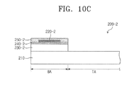
- FIGS. 10A to 10C are cross-sectional views showing a method of manufacturing a window member according to an exemplary embodiment of the present disclosure.
- FIGS. 10A to 10C show operations of manufacturing a window member corresponding to the operations shown in FIGS. 9B, 9C, and 9E .
- the same reference numerals denote the same elements in FIGS, 9 B, 9 C, and 9 E, and thus further descriptions of the same elements will be omitted.
- a liquid resin material is coated to be entirely overlapped with the bezel area BA of the cover glass 210 .
- the liquid resin material is cured to form a resin layer 230 - 2 .
- An uncured material RS 1 or a foreign substance RS 2 such as dust may remain in the transmission area TA of the cover glass 210 or the resin layer 230 - 2 in the curing process.
- a cleaning process is performed to remove the uncured material RS 1 or the foreign substance RS 2 .
- the inorganic layer 240 - 2 , the pattern layer 220 - 2 , and the bottom layer 250 - 2 are sequentially formed on the resin layer 230 - 2 .
- the inorganic layer 240 - 2 may be formed by depositing a metal oxide on the resin layer 230 - 2 .
- the pattern layer 220 - 2 is formed on the inorganic layer 240 - 2
- the pattern layer 220 - 2 is formed by depositing a non-transparent material on the inorganic layer 240 - 2 or by patterning an organic material. Since the pattern layer 220 - 2 is formed after the cleaning process, the pattern layer 220 - 2 is prevented from being detached or damaged due to the cleaning material CM.
- the bottom layer 250 - 2 is formed to cover the inorganic layer 240 - 2 and the pattern layer 220 - 2 .
- the bottom layer 250 - 2 is formed by depositing a non-transparent material.
- the bottom layer 250 - 2 may be formed by patterning an organic material.
- the bottom layer 250 - 2 is formed to entirely cover the pattern layer 220 - 2 .
Applications Claiming Priority (2)
| Application Number | Priority Date | Filing Date | Title |
|---|---|---|---|
| KR1020160003274A KR102495325B1 (ko) | 2016-01-11 | 2016-01-11 | 윈도우 부재 및 이의 제조 방법 |
| KR10-2016-0003274 | 2016-01-11 |
Publications (2)
| Publication Number | Publication Date |
|---|---|
| US20170200914A1 US20170200914A1 (en) | 2017-07-13 |
| US10490769B2 true US10490769B2 (en) | 2019-11-26 |
Family
ID=59275988
Family Applications (1)
| Application Number | Title | Priority Date | Filing Date |
|---|---|---|---|
| US15/222,826 Active 2037-09-04 US10490769B2 (en) | 2016-01-11 | 2016-07-28 | Window member and method of manufacturing the same |
Country Status (2)
| Country | Link |
|---|---|
| US (1) | US10490769B2 (ko) |
| KR (1) | KR102495325B1 (ko) |
Families Citing this family (7)
| Publication number | Priority date | Publication date | Assignee | Title |
|---|---|---|---|---|
| CN108017287A (zh) * | 2016-10-31 | 2018-05-11 | 南昌欧菲光学技术有限公司 | 盖板玻璃层叠结构及其加工方法 |
| KR102547540B1 (ko) | 2018-02-14 | 2023-06-26 | 삼성전자주식회사 | 윈도우 글래스 및 이를 구비하는 전자 장치 |
| KR102580450B1 (ko) * | 2018-06-22 | 2023-09-20 | 삼성디스플레이 주식회사 | 표시모듈, 표시패널 및 그 제조방법 |
| KR102640704B1 (ko) * | 2018-08-02 | 2024-02-27 | 삼성전자 주식회사 | 커버 글라스 및 이를 포함하는 전자 장치 |
| KR20210060715A (ko) * | 2019-11-18 | 2021-05-27 | 삼성디스플레이 주식회사 | 표시 장치 및 이의 제조 방법 |
| KR20220023836A (ko) * | 2020-08-20 | 2022-03-03 | 삼성디스플레이 주식회사 | 표시장치 및 이를 포함하는 전자장치 |
| US20220377922A1 (en) * | 2021-05-21 | 2022-11-24 | Samsung Display Co., Ltd. | Display device and electronic device including the same |
Citations (9)
| Publication number | Priority date | Publication date | Assignee | Title |
|---|---|---|---|---|
| KR20050094993A (ko) | 2004-03-24 | 2005-09-29 | (주)에스알 아이텍 | 축광안료를 이용한 윈도우 명판 및 제조방법 |
| KR20050106948A (ko) | 2004-05-06 | 2005-11-11 | 주식회사 엘엔씨테크 | 전기통신제품용 외장패널 및 그 제조방법 |
| KR100909835B1 (ko) | 2006-12-30 | 2009-07-29 | 주식회사 모젬 | 표시장치의 윈도우 제조방법, 표시장치 윈도우 및 이를구비한 휴대형 무선 단말기 |
| KR20100058944A (ko) | 2008-11-25 | 2010-06-04 | 조희봉 | 입체 윈도우 글라스 제조방법 및 그 제조물 |
| KR101212345B1 (ko) | 2009-04-27 | 2012-12-13 | 파나소닉 액정 디스플레이 주식회사 | 액정 표시 장치 |
| US20140079917A1 (en) * | 2012-09-20 | 2014-03-20 | Wen-Fu Huang | Device having multiple printing layers and a printing method thereof |
| US20140184525A1 (en) * | 2012-12-27 | 2014-07-03 | Samsung Electro-Mechanics Co., Ltd. | Touch panel and method for manufacturing the same |
| KR101457698B1 (ko) | 2008-05-28 | 2014-11-03 | 엘지전자 주식회사 | 표시장치의 화면 보호용 윈도우 |
| US20150103271A1 (en) * | 2013-10-10 | 2015-04-16 | Samsung Electro-Mechanics Co., Ltd. | Touch sensor |
Family Cites Families (2)
| Publication number | Priority date | Publication date | Assignee | Title |
|---|---|---|---|---|
| KR101984245B1 (ko) * | 2012-12-13 | 2019-05-31 | 삼성디스플레이 주식회사 | 유기 발광 표시 장치 |
| US8841174B1 (en) * | 2013-07-01 | 2014-09-23 | International Business Machines Corporation | Silicon controlled rectifier with integral deep trench capacitor |
-
2016
- 2016-01-11 KR KR1020160003274A patent/KR102495325B1/ko active IP Right Grant
- 2016-07-28 US US15/222,826 patent/US10490769B2/en active Active
Patent Citations (9)
| Publication number | Priority date | Publication date | Assignee | Title |
|---|---|---|---|---|
| KR20050094993A (ko) | 2004-03-24 | 2005-09-29 | (주)에스알 아이텍 | 축광안료를 이용한 윈도우 명판 및 제조방법 |
| KR20050106948A (ko) | 2004-05-06 | 2005-11-11 | 주식회사 엘엔씨테크 | 전기통신제품용 외장패널 및 그 제조방법 |
| KR100909835B1 (ko) | 2006-12-30 | 2009-07-29 | 주식회사 모젬 | 표시장치의 윈도우 제조방법, 표시장치 윈도우 및 이를구비한 휴대형 무선 단말기 |
| KR101457698B1 (ko) | 2008-05-28 | 2014-11-03 | 엘지전자 주식회사 | 표시장치의 화면 보호용 윈도우 |
| KR20100058944A (ko) | 2008-11-25 | 2010-06-04 | 조희봉 | 입체 윈도우 글라스 제조방법 및 그 제조물 |
| KR101212345B1 (ko) | 2009-04-27 | 2012-12-13 | 파나소닉 액정 디스플레이 주식회사 | 액정 표시 장치 |
| US20140079917A1 (en) * | 2012-09-20 | 2014-03-20 | Wen-Fu Huang | Device having multiple printing layers and a printing method thereof |
| US20140184525A1 (en) * | 2012-12-27 | 2014-07-03 | Samsung Electro-Mechanics Co., Ltd. | Touch panel and method for manufacturing the same |
| US20150103271A1 (en) * | 2013-10-10 | 2015-04-16 | Samsung Electro-Mechanics Co., Ltd. | Touch sensor |
Also Published As
| Publication number | Publication date |
|---|---|
| KR102495325B1 (ko) | 2023-02-03 |
| US20170200914A1 (en) | 2017-07-13 |
| KR20170084403A (ko) | 2017-07-20 |
Similar Documents
| Publication | Publication Date | Title |
|---|---|---|
| US10490769B2 (en) | Window member and method of manufacturing the same | |
| US11740716B2 (en) | Disposition structure of sensor of electronic device | |
| US10804485B2 (en) | Display apparatus | |
| US10355237B2 (en) | Electronic device and display module provided therein | |
| US10416718B2 (en) | Flexible display panel and flexible display apparatus | |
| US9022611B2 (en) | Display device and method for fabricating the same | |
| US8269732B2 (en) | Portable terminal | |
| US10721830B2 (en) | Waterproof display device and portable terminal | |
| KR101984161B1 (ko) | 터치스크린 패널 및 이를 구비한 휴대 단말기 | |
| US10485119B2 (en) | Display device and method of manufacturing window member | |
| US9915979B2 (en) | Input device, display device, electronic device, and mobile terminal | |
| JP2019133935A (ja) | 表示装置 | |
| JP5095043B1 (ja) | 入力機能付き表示装置、および電子機器 | |
| US10664014B2 (en) | Flexible display panel and flexible display apparatus | |
| US10861908B2 (en) | Display device | |
| KR102567498B1 (ko) | 커버 윈도우 및 이를 포함하는 표시장치 | |
| CN109413246B (zh) | 壳体组件及电子设备 | |
| CN104704458A (zh) | 输入装置、显示装置以及电子设备 | |
| US9137906B2 (en) | Mobile terminal | |
| KR20120021721A (ko) | 휴대 단말기 및 그의 디스플레이 모듈 | |
| KR101480454B1 (ko) | 휴대 단말기 | |
| US11529789B2 (en) | Mobile terminal | |
| CN108494910B (zh) | 显示屏组件、电子设备及显示屏组件的组装方法 | |
| KR102018228B1 (ko) | 이동 단말기 및 이의 제조 방법 | |
| CN106301438A (zh) | 智能终端 |
Legal Events
| Date | Code | Title | Description |
|---|---|---|---|
| AS | Assignment |
Owner name: SAMSUNG DISPLAY CO., LTD., KOREA, REPUBLIC OF Free format text: ASSIGNMENT OF ASSIGNORS INTEREST;ASSIGNOR:MIN, MYUNGAN;REEL/FRAME:039344/0232 Effective date: 20160608 |
|
| STPP | Information on status: patent application and granting procedure in general |
Free format text: RESPONSE TO NON-FINAL OFFICE ACTION ENTERED AND FORWARDED TO EXAMINER |
|
| STPP | Information on status: patent application and granting procedure in general |
Free format text: FINAL REJECTION MAILED |
|
| STPP | Information on status: patent application and granting procedure in general |
Free format text: RESPONSE AFTER FINAL ACTION FORWARDED TO EXAMINER |
|
| STPP | Information on status: patent application and granting procedure in general |
Free format text: NOTICE OF ALLOWANCE MAILED -- APPLICATION RECEIVED IN OFFICE OF PUBLICATIONS |
|
| STPP | Information on status: patent application and granting procedure in general |
Free format text: PUBLICATIONS -- ISSUE FEE PAYMENT VERIFIED |
|
| STCF | Information on status: patent grant |
Free format text: PATENTED CASE |
|
| CC | Certificate of correction | ||
| MAFP | Maintenance fee payment |
Free format text: PAYMENT OF MAINTENANCE FEE, 4TH YEAR, LARGE ENTITY (ORIGINAL EVENT CODE: M1551); ENTITY STATUS OF PATENT OWNER: LARGE ENTITY Year of fee payment: 4 |