US10466555B2 - LCD device - Google Patents
LCD device Download PDFInfo
- Publication number
- US10466555B2 US10466555B2 US15/761,428 US201615761428A US10466555B2 US 10466555 B2 US10466555 B2 US 10466555B2 US 201615761428 A US201615761428 A US 201615761428A US 10466555 B2 US10466555 B2 US 10466555B2
- Authority
- US
- United States
- Prior art keywords
- gate
- source
- liquid crystal
- crystal display
- display device
- Prior art date
- Legal status (The legal status is an assumption and is not a legal conclusion. Google has not performed a legal analysis and makes no representation as to the accuracy of the status listed.)
- Active
Links
Images


Classifications
-
- G—PHYSICS
- G02—OPTICS
- G02F—OPTICAL DEVICES OR ARRANGEMENTS FOR THE CONTROL OF LIGHT BY MODIFICATION OF THE OPTICAL PROPERTIES OF THE MEDIA OF THE ELEMENTS INVOLVED THEREIN; NON-LINEAR OPTICS; FREQUENCY-CHANGING OF LIGHT; OPTICAL LOGIC ELEMENTS; OPTICAL ANALOGUE/DIGITAL CONVERTERS
- G02F1/00—Devices or arrangements for the control of the intensity, colour, phase, polarisation or direction of light arriving from an independent light source, e.g. switching, gating or modulating; Non-linear optics
- G02F1/01—Devices or arrangements for the control of the intensity, colour, phase, polarisation or direction of light arriving from an independent light source, e.g. switching, gating or modulating; Non-linear optics for the control of the intensity, phase, polarisation or colour
- G02F1/13—Devices or arrangements for the control of the intensity, colour, phase, polarisation or direction of light arriving from an independent light source, e.g. switching, gating or modulating; Non-linear optics for the control of the intensity, phase, polarisation or colour based on liquid crystals, e.g. single liquid crystal display cells
- G02F1/133—Constructional arrangements; Operation of liquid crystal cells; Circuit arrangements
- G02F1/136—Liquid crystal cells structurally associated with a semi-conducting layer or substrate, e.g. cells forming part of an integrated circuit
- G02F1/1362—Active matrix addressed cells
- G02F1/136286—Wiring, e.g. gate line, drain line
-
- G—PHYSICS
- G02—OPTICS
- G02F—OPTICAL DEVICES OR ARRANGEMENTS FOR THE CONTROL OF LIGHT BY MODIFICATION OF THE OPTICAL PROPERTIES OF THE MEDIA OF THE ELEMENTS INVOLVED THEREIN; NON-LINEAR OPTICS; FREQUENCY-CHANGING OF LIGHT; OPTICAL LOGIC ELEMENTS; OPTICAL ANALOGUE/DIGITAL CONVERTERS
- G02F1/00—Devices or arrangements for the control of the intensity, colour, phase, polarisation or direction of light arriving from an independent light source, e.g. switching, gating or modulating; Non-linear optics
- G02F1/01—Devices or arrangements for the control of the intensity, colour, phase, polarisation or direction of light arriving from an independent light source, e.g. switching, gating or modulating; Non-linear optics for the control of the intensity, phase, polarisation or colour
- G02F1/13—Devices or arrangements for the control of the intensity, colour, phase, polarisation or direction of light arriving from an independent light source, e.g. switching, gating or modulating; Non-linear optics for the control of the intensity, phase, polarisation or colour based on liquid crystals, e.g. single liquid crystal display cells
- G02F1/133—Constructional arrangements; Operation of liquid crystal cells; Circuit arrangements
- G02F1/1333—Constructional arrangements; Manufacturing methods
- G02F1/1345—Conductors connecting electrodes to cell terminals
- G02F1/13452—Conductors connecting driver circuitry and terminals of panels
-
- G—PHYSICS
- G09—EDUCATION; CRYPTOGRAPHY; DISPLAY; ADVERTISING; SEALS
- G09G—ARRANGEMENTS OR CIRCUITS FOR CONTROL OF INDICATING DEVICES USING STATIC MEANS TO PRESENT VARIABLE INFORMATION
- G09G3/00—Control arrangements or circuits, of interest only in connection with visual indicators other than cathode-ray tubes
- G09G3/20—Control arrangements or circuits, of interest only in connection with visual indicators other than cathode-ray tubes for presentation of an assembly of a number of characters, e.g. a page, by composing the assembly by combination of individual elements arranged in a matrix no fixed position being assigned to or needed to be assigned to the individual characters or partial characters
- G09G3/34—Control arrangements or circuits, of interest only in connection with visual indicators other than cathode-ray tubes for presentation of an assembly of a number of characters, e.g. a page, by composing the assembly by combination of individual elements arranged in a matrix no fixed position being assigned to or needed to be assigned to the individual characters or partial characters by control of light from an independent source
- G09G3/36—Control arrangements or circuits, of interest only in connection with visual indicators other than cathode-ray tubes for presentation of an assembly of a number of characters, e.g. a page, by composing the assembly by combination of individual elements arranged in a matrix no fixed position being assigned to or needed to be assigned to the individual characters or partial characters by control of light from an independent source using liquid crystals
- G09G3/3611—Control of matrices with row and column drivers
- G09G3/3614—Control of polarity reversal in general
-
- G—PHYSICS
- G09—EDUCATION; CRYPTOGRAPHY; DISPLAY; ADVERTISING; SEALS
- G09G—ARRANGEMENTS OR CIRCUITS FOR CONTROL OF INDICATING DEVICES USING STATIC MEANS TO PRESENT VARIABLE INFORMATION
- G09G3/00—Control arrangements or circuits, of interest only in connection with visual indicators other than cathode-ray tubes
- G09G3/20—Control arrangements or circuits, of interest only in connection with visual indicators other than cathode-ray tubes for presentation of an assembly of a number of characters, e.g. a page, by composing the assembly by combination of individual elements arranged in a matrix no fixed position being assigned to or needed to be assigned to the individual characters or partial characters
- G09G3/34—Control arrangements or circuits, of interest only in connection with visual indicators other than cathode-ray tubes for presentation of an assembly of a number of characters, e.g. a page, by composing the assembly by combination of individual elements arranged in a matrix no fixed position being assigned to or needed to be assigned to the individual characters or partial characters by control of light from an independent source
- G09G3/36—Control arrangements or circuits, of interest only in connection with visual indicators other than cathode-ray tubes for presentation of an assembly of a number of characters, e.g. a page, by composing the assembly by combination of individual elements arranged in a matrix no fixed position being assigned to or needed to be assigned to the individual characters or partial characters by control of light from an independent source using liquid crystals
- G09G3/3611—Control of matrices with row and column drivers
- G09G3/3674—Details of drivers for scan electrodes
- G09G3/3677—Details of drivers for scan electrodes suitable for active matrices only
-
- G—PHYSICS
- G09—EDUCATION; CRYPTOGRAPHY; DISPLAY; ADVERTISING; SEALS
- G09G—ARRANGEMENTS OR CIRCUITS FOR CONTROL OF INDICATING DEVICES USING STATIC MEANS TO PRESENT VARIABLE INFORMATION
- G09G3/00—Control arrangements or circuits, of interest only in connection with visual indicators other than cathode-ray tubes
- G09G3/20—Control arrangements or circuits, of interest only in connection with visual indicators other than cathode-ray tubes for presentation of an assembly of a number of characters, e.g. a page, by composing the assembly by combination of individual elements arranged in a matrix no fixed position being assigned to or needed to be assigned to the individual characters or partial characters
- G09G3/34—Control arrangements or circuits, of interest only in connection with visual indicators other than cathode-ray tubes for presentation of an assembly of a number of characters, e.g. a page, by composing the assembly by combination of individual elements arranged in a matrix no fixed position being assigned to or needed to be assigned to the individual characters or partial characters by control of light from an independent source
- G09G3/36—Control arrangements or circuits, of interest only in connection with visual indicators other than cathode-ray tubes for presentation of an assembly of a number of characters, e.g. a page, by composing the assembly by combination of individual elements arranged in a matrix no fixed position being assigned to or needed to be assigned to the individual characters or partial characters by control of light from an independent source using liquid crystals
- G09G3/3611—Control of matrices with row and column drivers
- G09G3/3685—Details of drivers for data electrodes
- G09G3/3688—Details of drivers for data electrodes suitable for active matrices only
-
- H—ELECTRICITY
- H01—ELECTRIC ELEMENTS
- H01L—SEMICONDUCTOR DEVICES NOT COVERED BY CLASS H10
- H01L27/00—Devices consisting of a plurality of semiconductor or other solid-state components formed in or on a common substrate
- H01L27/02—Devices consisting of a plurality of semiconductor or other solid-state components formed in or on a common substrate including semiconductor components specially adapted for rectifying, oscillating, amplifying or switching and having at least one potential-jump barrier or surface barrier; including integrated passive circuit elements with at least one potential-jump barrier or surface barrier
- H01L27/12—Devices consisting of a plurality of semiconductor or other solid-state components formed in or on a common substrate including semiconductor components specially adapted for rectifying, oscillating, amplifying or switching and having at least one potential-jump barrier or surface barrier; including integrated passive circuit elements with at least one potential-jump barrier or surface barrier the substrate being other than a semiconductor body, e.g. an insulating body
- H01L27/1214—Devices consisting of a plurality of semiconductor or other solid-state components formed in or on a common substrate including semiconductor components specially adapted for rectifying, oscillating, amplifying or switching and having at least one potential-jump barrier or surface barrier; including integrated passive circuit elements with at least one potential-jump barrier or surface barrier the substrate being other than a semiconductor body, e.g. an insulating body comprising a plurality of TFTs formed on a non-semiconducting substrate, e.g. driving circuits for AMLCDs
- H01L27/124—Devices consisting of a plurality of semiconductor or other solid-state components formed in or on a common substrate including semiconductor components specially adapted for rectifying, oscillating, amplifying or switching and having at least one potential-jump barrier or surface barrier; including integrated passive circuit elements with at least one potential-jump barrier or surface barrier the substrate being other than a semiconductor body, e.g. an insulating body comprising a plurality of TFTs formed on a non-semiconducting substrate, e.g. driving circuits for AMLCDs with a particular composition, shape or layout of the wiring layers specially adapted to the circuit arrangement, e.g. scanning lines in LCD pixel circuits
-
- G—PHYSICS
- G02—OPTICS
- G02F—OPTICAL DEVICES OR ARRANGEMENTS FOR THE CONTROL OF LIGHT BY MODIFICATION OF THE OPTICAL PROPERTIES OF THE MEDIA OF THE ELEMENTS INVOLVED THEREIN; NON-LINEAR OPTICS; FREQUENCY-CHANGING OF LIGHT; OPTICAL LOGIC ELEMENTS; OPTICAL ANALOGUE/DIGITAL CONVERTERS
- G02F2203/00—Function characteristic
- G02F2203/01—Function characteristic transmissive
-
- G—PHYSICS
- G09—EDUCATION; CRYPTOGRAPHY; DISPLAY; ADVERTISING; SEALS
- G09G—ARRANGEMENTS OR CIRCUITS FOR CONTROL OF INDICATING DEVICES USING STATIC MEANS TO PRESENT VARIABLE INFORMATION
- G09G2300/00—Aspects of the constitution of display devices
- G09G2300/04—Structural and physical details of display devices
- G09G2300/0421—Structural details of the set of electrodes
- G09G2300/0426—Layout of electrodes and connections
-
- G—PHYSICS
- G09—EDUCATION; CRYPTOGRAPHY; DISPLAY; ADVERTISING; SEALS
- G09G—ARRANGEMENTS OR CIRCUITS FOR CONTROL OF INDICATING DEVICES USING STATIC MEANS TO PRESENT VARIABLE INFORMATION
- G09G2310/00—Command of the display device
- G09G2310/02—Addressing, scanning or driving the display screen or processing steps related thereto
- G09G2310/0243—Details of the generation of driving signals
- G09G2310/0254—Control of polarity reversal in general, other than for liquid crystal displays
-
- G—PHYSICS
- G09—EDUCATION; CRYPTOGRAPHY; DISPLAY; ADVERTISING; SEALS
- G09G—ARRANGEMENTS OR CIRCUITS FOR CONTROL OF INDICATING DEVICES USING STATIC MEANS TO PRESENT VARIABLE INFORMATION
- G09G2310/00—Command of the display device
- G09G2310/02—Addressing, scanning or driving the display screen or processing steps related thereto
- G09G2310/0264—Details of driving circuits
- G09G2310/0278—Details of driving circuits arranged to drive both scan and data electrodes
-
- G—PHYSICS
- G09—EDUCATION; CRYPTOGRAPHY; DISPLAY; ADVERTISING; SEALS
- G09G—ARRANGEMENTS OR CIRCUITS FOR CONTROL OF INDICATING DEVICES USING STATIC MEANS TO PRESENT VARIABLE INFORMATION
- G09G2310/00—Command of the display device
- G09G2310/06—Details of flat display driving waveforms
- G09G2310/061—Details of flat display driving waveforms for resetting or blanking
-
- G—PHYSICS
- G09—EDUCATION; CRYPTOGRAPHY; DISPLAY; ADVERTISING; SEALS
- G09G—ARRANGEMENTS OR CIRCUITS FOR CONTROL OF INDICATING DEVICES USING STATIC MEANS TO PRESENT VARIABLE INFORMATION
- G09G2320/00—Control of display operating conditions
- G09G2320/02—Improving the quality of display appearance
- G09G2320/0223—Compensation for problems related to R-C delay and attenuation in electrodes of matrix panels, e.g. in gate electrodes or on-substrate video signal electrodes
-
- G—PHYSICS
- G09—EDUCATION; CRYPTOGRAPHY; DISPLAY; ADVERTISING; SEALS
- G09G—ARRANGEMENTS OR CIRCUITS FOR CONTROL OF INDICATING DEVICES USING STATIC MEANS TO PRESENT VARIABLE INFORMATION
- G09G2330/00—Aspects of power supply; Aspects of display protection and defect management
- G09G2330/10—Dealing with defective pixels
Definitions
- the present invention relates to a high-speed-drive liquid crystal display device.
- a liquid crystal display device configured to be driven by a color-field sequential system requires a driving speed several times as high as the driving speed of a liquid crystal display device configured to be driven by a common driving system.
- the color-field sequential system denotes a driving system for controlling a liquid crystal panel to sequentially display subframes in synchronism with a lighting timing of backlights.
- the subframes correspond to the respective three primary colors.
- the backlights correspond to the respective three primary colors.
- PTL 1 discloses a technique for sufficiently charging all pixels in a high-speed-drive liquid crystal display device.
- a horizontal scanning period corresponding to the positive polarity in which charging is difficult (sufficient charging requires time) is increased, and a horizontal scanning period corresponding to the negative polarity is reduced.
- the sum of one horizontal scanning period corresponding to the positive polarity and one horizontal scanning period corresponding to the negative polarity equals two horizontal scanning periods in a common driving system. This enables all pixels to be sufficiently charged while a decrease in driving speed of the liquid crystal display device is suppressed.
- a source line closer to a source driver has a smaller time constant.
- a pixel closer to the source driver requires a shorter charging time.
- a reason why the source line closer to the source driver has a smaller time constant is as follows. That is, the closer the source driver, the shorter the wiring length of the source line, and thus, the resistance value becomes small, which leads to a smaller time constant.
- the resistance value is large correspondingly to the entire length of the source line, which leads to a large time constant. Note that a capacity component has substantially the same value even when the distance from the source driver varies.
- a conventional liquid crystal display device does not take the relationship between the distance of each pixel to the source driver and the time required to charge each pixel into consideration. Thus, charging pixels closer to the source driver take an unnecessarily longer time. The unnecessarily longer time hinders high-speed driving of the liquid crystal display device.
- PTL 1 proposes a driving method adopting a polarity arrangement similar to the dot inversion driving, but the driving method cannot fully achieve the dot inversion driving. This is because in the driving method, a line of negative polarity in a row (a line reducing the horizontal scanning period) has to be included in the polarity arrangement. Thus, applying the liquid crystal driving method according to PTL 1 to the dot inversion driving is difficult.
- a liquid crystal display device includes: a plurality of first gate lines; a plurality of first source lines disposed to intersect the plurality of first gate lines; a first pixel formed at least one of intersections of the plurality of first gate lines and the plurality of first source lines; a first source driver configured to supply a first drive signal to end parts of the plurality of first source lines to drive the plurality of first source lines, wherein the plurality of first gate lines include a first group including one or a plurality of the first gate lines adjacent to each other, the first group including at least a first proximal gate line which is the first gate line closest to the first source driver, and a second group including one or a plurality of the first gate lines adjacent to each other, the second group being disposed on an opposite side of the first group from the source driver, and at least all the first gate lines included in the first group except for the first proximal gate line each have a shorter driving time in one frame than each of the first gate lines included in
- the one aspect of the present in enables a high-speed-drive liquid crystal display device easily applicable to dot inversion driving to be realized.
- FIG. 1 is a timing chart illustrating driving of a liquid crystal display device according to a first embodiment of the present invention.
- FIG. 2 is a block diagram illustrating main components of the liquid crystal display device according to the first embodiment of the present invention.
- FIG. 3 is a timing chart illustrating driving of a liquid crystal display device according to a comparative example.
- FIG. 4 is a timing chart illustrating how video data is converted along with the driving illustrated in FIG. 1 .
- FIG. 5 is a block diagram illustrating main components of a liquid crystal display device according to a second embodiment of the present invention.
- FIG. 6 is a timing chart illustrating driving of the liquid crystal display device according to the second embodiment of the present invention.
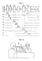
- FIG. 7 is a timing chart illustrating driving of a liquid crystal display device according to a third embodiment of the present invention.
- FIG. 8 is a view illustrating a liquid crystal display device according to a fourth embodiment of the present invention and the usage example of the liquid crystal display device.
- FIG. 1 is a timing chart illustrating driving of a liquid crystal display device 100 according to a first embodiment of the present invention.
- FIG. 2 is a block diagram illustrating main components of the liquid crystal display device 100 according to the first embodiment of the present invention.
- the liquid crystal display device 100 includes n (a plurality of) gate lines (first gate lines) GL, p (a plurality of) source lines (first source line) SL, a plurality of transistors T and pixels (first pixels) P, a gate driver 1 , and a source driver (first source driver) 2 .
- the gate lines GL are arranged to intersect the source lines SL.
- the gate lines GL are arranged from a side where the source driver 2 is provided, that is, from top to bottom in the order of a gate line (first proximal gate line) GL 1 , a gate line GL 2 , . . . , a gate line GL(n ⁇ 1), and a gate line GLn.
- the source lines SL are arranged in the order of a source line SL 1 , a source line SL 2 , . . . , and a source line SLp from the gate driver 1 .
- the transistor T and the pixel P are formed at least one of intersections of the n gate lines GL and the p source lines SL.
- the gate of the transistor S is connected to the gate line GL
- the source of the transistor T is connected to the source line SL
- the pixel P is connected to the drain of the transistor T.
- the p source lines SL are arranged from the source line SL 1 to the source line SLp in the order of a source line SL_OE, a source line SL_EO, a source line SL_EO, and a source line SL_OE for each four source lines SL.
- Different signals may be supplied to the p source lines SL, but one of any two adjacent pixels of the plurality of pixels P is driven by the source line SL_OE, and the other of the two adjacent pixels is driven by the source line SL_EO.
- a connection relationship between each source line SL and each transistor T and pixel P is determined so as to be able to realize such driving.
- pixel groups P 1 to Pn are defined.
- the pixel groups P 1 to Pn are collections of the pixels P connected to the gate lines GL 1 to GLn respectively via the corresponding transistors T.
- the gate driver 1 is disposed on a side of the source line SL 1 and is configured to supply a gate drive signal to the n gate lines GL to drive the n gate lines GL.
- the source driver 2 is disposed on an upper side of the gate line GL 1 and is configured to supply a source drive signal (first drive signal) to the p source lines SL to drive the p source lines SL.
- the liquid crystal display device 100 is driven by dot inversion driving and so-called double-source driving.
- the dot inversion driving enables desired image quality to be secured even in a case of a large-size liquid crystal display device, typically, a television set. That is, the gate driver 1 and the source driver 2 operate as described below.
- the gate driver 1 is configured to supply an identical gate drive signal to the gate lines GL 1 and the gate lines GL 2 .
- the gate driver 1 is connected to a common gate line GL 12 to which the gate drive signal for driving the gate line GL 1 and the gate line GL 2 is supplied.
- the common gate line GL 12 is separated into the gate line GL 1 and the gate line GL 2 .
- the pixels P belonging to the pixel group P 1 and the pixels P belonging to the pixel group P 2 are brought into an on state at the same timing.
- the gate driver 1 and each gate line GL are configured such that similarly to the combination of the gate line GL 1 and the gate line GL 2 , an identical gate drive signal is supplied to each of a combination of the gate line GL 3 and the gate line GL 4 , . . . , and a combination of the gate line GL(n ⁇ 1) and the gate line GLn.
- the source driver 2 is configured to supply an identical source drive signal to the source lines SL_OE and to supply an identical source drive signal to the source lines SL_EO.
- the source lines SL_OE are driven such that the source drive signal of the source lines SL_OE corresponds to the positive polarity
- the source lines SL_EC are driven such that the source drive signal of the source lines SL_EO corresponds to the negative polarity.
- the source lines SL_OE are driven such that the source drive signal of the source lines SL_OE corresponds to the negative polarity
- the source lines SL_EO are driven such that the source drive signal of the source lines SL_EO corresponds to the positive polarity.
- any two adjacent pixels of the plurality of pixels P are in a relationship of inversion polarity (i.e., one of the two pixels has the positive polarity and the other of the two pixels has the negative polarity).
- the dot inversion driving is realized.
- the source lines SL closer to the source driver 2 have smaller time constants, and thus the pixels P closer to the source driver 2 require shorter charging times. That is, in the liquid crystal display device 100 , a time required to charge the pixels P belonging to the pixel group P 1 is shortest, and the time required to charge the pixels P increases in the order of the pixels P belonging to the pixel group P 2 , . . . , the pixels P belonging to the pixel group Pn. Thus, in order to realize high-speed driving of the liquid crystal display device 100 , the liquid crystal display device 100 is driven as described below according to the timing chart shown in FIG. 1 .
- the period t 1 is a period corresponding to one frame of the liquid crystal display device 100 .
- a gate drive signal GSA is a gate drive signal for driving the gate line GL 1 and the gate line GL 2 (in other words, supplied to the common gate line GL 12 ).
- a gate drive signal GSB is a gate drive signal for driving the gate line GL 3 and the gate line GL 4 .
- a gate drive signal GSC is a gate drive signal for driving the gate line GL 5 and the gate line GL 6 .
- the gate drive signal GSA, the gate drive signal GSB, and the gate drive signal GSC are pulse signals.
- the pulse width of the gate drive signal GSA, the pulse width of the gate drive signal GSB, and the pulse width of the gate drive signal GSC are equal to one another and are each a pulse width GSa.
- the gate lines GL 1 to GL 6 correspond to a first group. Moreover, the gate lines GL 1 and GL 2 correspond to a first subgroup, and the gate lines GL 3 to GL 6 corresponds to a second subgroup. Moreover, the gate line GL 1 is a gate line of the gate lines GL which is closest to the source driver 2 , and thus, as described above, the gate line GL 1 corresponds to the first proximal gate line.
- a gate drive signal GSQ is a gate drive signal for driving the gate line GLm and the gate line GL(m+1).
- a gate drive signal GSR is a gate drive signal for driving the gate line GL(m+2) and the gate line GL(m+3).
- a gate drive signal GSS is a gate drive signal for driving the gate line GL(m+4) and the gate line GL(m+5). Note that m is an integer larger than or equal to seven, and m+5 is smaller than or equal to n ⁇ 6.
- the gate drive signal GSQ, the gate drive signal GSR, and the gate drive signal GSS are pulse signals.
- the pulse width of the gate drive signal GSQ, the pulse width of the gate drive signal GSR, and the pulse width of the gate drive signal GSS are equal to one another and are each a pulse width GSq.
- the gate lines GLm to CL(m+5) correspond to one of the second groups.
- a gate drive signal GSX is a gate drive signal for driving the gate line GL(n ⁇ 5) and the gate line GL(n ⁇ 4).
- a gate drive signal GSY is a gate drive signal for driving the gate line GL(n ⁇ 3) and the gate line GL(n ⁇ 2).
- a gate drive signal GSZ is a gate drive signal for driving the gate line GL(n ⁇ 1) and the gate line GLn.
- the gate drive signal GSX, the gate drive signal GSY, and the gate drive signal GSZ are pulse signals.
- the pulse width of the gate drive signal GSX, the pulse width of the gate drive signal GSY, and the pulse width of the gate drive signal GSZ are equal to one another and are each a pulse width GSx.
- the gate lines GL(n ⁇ 5) to GLn correspond to another one of the second groups.
- the pulse width GSa, the pulse width GSq, and the pulse width GSx are in the following relationship: pulse width GSa ⁇ pulse width GSq ⁇ pulse width GSx.
- the drive time of each of the gate lines GL 1 to GL 6 defined by the pulse width GSa is shorter than the drive time of each of the gate lines GLm to GL(m+5) defined by the pulse width GSq.
- the drive time of each of the gate lines GL 1 to GL 6 and the drive time of each of the gate lines GLm to GL(m+5) are each shorter than the drive time of each of the gate line GL(n ⁇ 5) to GLn defined by the pulse width GSx.
- each of the first group and two second groups includes six gate lines GL adjacent to each other. Note that the number of the gate lines GL included in the first group and the number of gate lines GL included in each second group are each at least one.
- a potential COM denotes a potential of a counter electrode (not shown) included in the liquid crystal display device 100 .
- a signal SS_OE denotes the source drive signal in each source line SL_OE which the source driver 2 outputs
- a signal SS_EO denotes the source drive signal in each source line SL_EO which the source driver 2 outputs.
- a potential VP_OE denotes the potential of a pixel electrode (not shown) of one of pixels P driven by the signal SS_OE
- a potential VP_EO denotes the potential of a pixel electrode of one of pixels P driven by the signal SS_EO.
- the signal SS_OE rises at a rising timing of the gate drive GSA, and then, the signal SS_OE repeatedly falls and rises in synchronism with a rise of each of the gate drive signals GSB to GSZ.
- the signal SS_EO falls at the rising timing of the gate drive signal GSA, and then, the signal SS_EO repeatedly rises and falls in synchronism with a rise of each of the gate drive signals GSB to GSZ.
- Each of the signal SS_OE and the signal SS_EO charges a corresponding one of the pixels P with the positive polarity during a period from the start of a rise to the start of a next fall and charges the corresponding one of the pixels P with the negative polarity during a period from the start of a fall to the start of a next rise.
- a period of one pulse of the signal SS_OE and the signal SS_EO corresponding to the gate drive signal GSA is defined as a period SSa.
- a period of one pulse of the signal SS_OE and the signal SS_EO corresponding to the gate drive signal GSQ is defined as a period SSq.
- a period of one pulse of the signal SS_OE and the signal SS_EO corresponding to the gate drive signal GSX is defined as a period SSx.
- the period SSa pulse width GSa
- the period SSq pulse width GSq
- the period SSx pulse width GSx
- the period SSx corresponds to a length of a period during which all the pixels P belonging to the pixel group Pn can be sufficiently charged by the signal SS_OE and the signal SS_EO.
- the distance of each pixel P to the source driver 2 and a time required to charge each pixel P are taken into consideration, and as the distance to the source driver 2 decreases, the charging time of each pixel P is reduced.
- FIG. 3 is a timing chart illustrating the driving of the liquid crystal display device according to the comparative example.
- gate drive signals GSA to GSZ have all the same pulse width.
- the pulse width (drive time) of each of the gate drive signals GSA to GSZ has to be the pulse width GSx shown in FIG. 1 .
- the period of one pulse of signal SS_OE and a signal SS_EO during charging of all pixels P belonging to pixel groups P 1 to P 6 is a period SSx.
- charging of all pixels P belonging to the pixel groups P 1 to P 6 is actually completed in the period SSa (see FIG. 1 ) shorter than the period SSx.
- a period obtained by subtracting The period SSa from the period SSx is a wasted period during the charging of all pixels P belonging to the pixel groups P 1 to P 6 .
- a period (in FIG. 3 , a period. SS(x-q)) obtained by subtracting the period SSx from the period SSq is a wasted period during the charging of all pixels P belonging to the pixel groups Pm to P(m+5).
- the period t 2 in FIG. 3 corresponding to one frame of the liquid crystal display device according to the comparative example also becomes longer than the above-described period t 1 shown in FIG. 1 .
- FIG. 4 is a timing chart illustrating how video data is converted along with the driving illustrated in FIG. 1 .
- the liquid crystal display device 100 includes a video processing circuit (e.g., a known timing controller) including frame memory.
- the frame memory accumulates data of one frame (how the data is accumulated is not shown).
- the data which is accumulated is synchronized with a clock which can be driven with a minimum gate line width ( FIG. 1 , the period SSa), and the data is supplied to the source device 2 .
- the period SSa is determined in accordance with a longer one of a time of scanning (CLK frequency) of one horizontal interval corresponding to the driving speed of the source driver 2 and a minimum time in which at least one pixel P can be charged.
- the timing controller transfers an operation clock CLK, a data enable signal DE, and an image data signal DATA (not shown) which are input to the timing controller to, for example, a higher-speed operation clock in the timing controller to generate a converted operation clock CLK′, a converted data enable signal DE′, and a converted image data signal DATA′ (not shown).
- the converted operation clock CLK′, the converted data enable signal DE′, and the converted image data signal DATA′ are driven constantly, and the pulse widths of these signals are adjusted by the blanking interval of one horizontal interval and the timing of a latch signal LS.
- the source driver 2 is a known source driver, the driving shown in FIG. 1 becomes possible.
- This method also enables driving with a pulse width larger than one horizontal interval of the input signal, and thus, the driving is possible even in a case of a liquid crystal panel in which the driving was previously not possible.
- the latch signal LS and the gate clock GCK are generated by a signal LGT (LS, GCK timing).
- the signal LGT is a signal read from a look-up table (LUT) or the like in which signals configured in accordance with the time constant at each control location of the liquid crystal display device 100 are stored.
- LUT look-up table
- toe pulse widths of the gate drive signals GSA to GSZ are reduced on a side adjacent to the source driver 2 and are increased on a side away from the source driver 2 in accordance with the time constants of the source lines SL.
- a period corresponding to one frame can be reduced from the period t 2 shown in FIG. 3 to the period t 1 shown in FIG. 1 .
- FIG. 5 is a block diagram illustrating main components of a liquid crystal display device 200 according to a second embodiment of the present invention.
- FIG. 6 is a timing chart illustrating driving of the liquid crystal display device 200 according to the second embodiment of the present invention.
- An liquid crystal display device 200 illustrated in FIG. 5 includes, in addition to the components of the liquid crystal display device 100 , n (a plurality of) gate lines (second gate lines) GL- 2 , p (a plurality of) source lines (second source line) SL- 2 , a plurality of transistors T- 2 and pixels (second pixels) P- 2 , a gate driver 1 - 2 , and a source driver (second source driver) 2 - 2 .
- the gate lines GL- 2 are arranged to intersect the source lines SL- 2 .
- the gate lines GL- 2 are arranged from a side where the source driver 2 - 2 is provided, that is, from bottom to top in the order of a gate line (second proximal gate line) GL 1 - 2 , a gate line GL 2 - 2 , . . . , a gate line GL(n ⁇ 1)- 2 , and a gate line GLn ⁇ 2.
- the source lines SL- 2 are arranged in the order of a source line SL 1 - 2 , a source line SL 2 - 2 , . . . , and a source line SLp- 2 from the gate driver 1 - 2 .
- the gate line GLn and the gate line GLn ⁇ 2 are adjacent to each other in the up-down direction.
- the transistor T- 2 and the pixel P- 2 are formed at least one of intersections of the n gate lines GL- 2 and the p source lines SL- 2 .
- the gate of the transistor T- 2 is connected to the gate line GL- 2
- the source of the transistor T- 2 is connected to the source line SL- 2
- the pixel P- 2 is connected to the drain of the transistor T- 2 .
- the p source lines SL- 2 are arranged from the source line SL 1 - 2 to the source line SLp- 2 in the order of a source line SL_OE- 2 , a source line SL_EO- 2 , a source line SL_EO- 2 , and a source line SL_OE- 2 for each four source lines SL- 2 .
- Different signals may be supplied to the p source lines SL- 2 , but one of any two adjacent pixels of the plurality of pixels P- 2 is driven by the source line SL_OE- 2 , and the other of the two adjacent pixels is driven by the source line SL_EO- 2 .
- a connection relationship between each source line SL- 2 and each transistor T- 2 and pixel P- 2 is determined so as to be able to realize such driving.
- pixel groups P 1 - 2 to Pn- 2 are defined.
- the pixel groups P 1 - 2 to Pn- 2 are collections of pixels P- 2 connected to the gate lines GL 1 - 2 to GLn- 2 respectively via the corresponding transistors T- 2 .
- the gate driver 1 - 2 is disposed on a side of the source line SL 1 - 2 and is configured to supply a gate drive signal to the n gate lines GL- 2 to drive the n gate lines GL- 2 .
- the source driver 2 - 2 is disposed on a lower side of the gate line GL 1 - 2 and is configured to supply a source drive signal (second drive signal) to the p source lines SL- 2 to drive the p source lines SL- 2 .
- the source drive signal supplied to the p source lines SL from the source driver 2 and the source drive signal supplied to the p source lines SL- 2 from the source driver 2 - 2 will be described later.
- the liquid crystal display device 200 is, similarly to the liquid crystal display device 100 , driven by dot inversion driving and double-source driving. That is, the gate driver 1 and the source driver 2 operate in a similar manner to those of the liquid crystal display device 100 , and the gate driver 1 - 2 and the source driver 2 - 2 operate as described below.
- the gate driver 1 - 2 is configured to supply an identical gate drive signal to the gate lines GL 1 - 2 and the gate lines GL 2 - 2 .
- the principle of the supply is the same as the principle that the gate driver 1 supplies an identical gate drive signal to the gate line GL 1 and the gate line GL 2 , and thus, the detailed description will be omitted in this embodiment.
- the gate driver 1 - 2 and each gate line GL- 2 are configured such that similarly to the combination of the gate line GL 1 - 2 and the gate line GL 2 - 2 , an identical gate drive signal is supplied to each of a combination of the gate line GL 3 - 2 and the gate line GL 4 - 2 , . . . , and a combination of the gate line GL(n ⁇ 1)- 2 and the gate line GLn- 2 .
- the source driver 2 - 2 is configured to supply an identical source drive signal to the source lines SL_OE- 2 and to supply an identical source drive signal to the source lines SL_EO- 2 based on a principle similar to the principle of the source driver 2 .
- any adjacent pixel P and pixel P- 2 respectively belonging to the pixel group Pn and the pixel group Pn- 2 are in a relationship of inverted polarity.
- the dot inversion driving is realized.
- the source lines SL- 2 closer to the source driver 2 - 2 have smaller time constants, and thus, the pixels P- 2 closer to the source driver 2 - 2 require shorter charging times. That is, in the liquid crystal display device 200 , a time required to charge the pixels P- 2 belonging to the pixel group P 1 - 2 is shortest, and the time required to charge the pixels P- 2 increases in the order of the pixels P- 2 belonging to the pixel group P 2 - 2 , . . . , the pixels P- 2 belonging to the pixel group Pn- 2 . Thus, in order to realize high-speed driving of the liquid crystal display device 200 , the liquid crystal display device 200 is driven as described below according to the timing chart shown in FIG. 6 .
- FIG. 6 is a figure in which the contents described below are added to the timing chart shown in FIG. 1 .
- a gate drive signal GSA- 2 is a gate drive signal for driving the gate line GL 1 - 2 and the gate line GL 2 - 2 .
- a gate drive signal GSB- 2 is a gate drive signal for driving the gate line GL 3 - 2 and the gate line GL 4 - 2 .
- a gate drive signal GSC- 2 is a gate drive signal for driving the gate line GL 5 - 2 and the gate line GL 6 - 2 .
- the gate drive signal GSA- 2 , the sate drive signal GSB- 2 , and the gate drive signal GSC- 2 have the same rising timing, falling timing, and pulse width (pulse width GSa) as the gate drive signal GSA, the gate drive signal GSB, and the gate drive signal GSC respectively.
- the gate lines GL 1 - 2 to GL 6 - 2 correspond to a third group.
- the gate line GL 1 - 2 is a gate line of the gate lines GL- 2 which is closest to the source driver 2 - 2 , and thus, as described above, the gate line GL 1 - 2 corresponds to the second proximal gate line.
- a gate drive signal GSQ- 2 is a gate drive signal for driving the gate line GLm- 2 and the gate line GL(m+1)- 2 .
- a gate drive signal CSR- 2 is a gate drive signal for driving the gate line GL(m+2)- 2 and the gate line GL(m+3)- 2 .
- a gate drive signal CSS- 2 is a gate drive signal for driving the gate line CL(m+4)- 2 and the gate line GL(m+5)- 2 .
- the gate drive signal GSQ- 2 , the gate drive signal GSR- 2 , and the gate drive signal GSS- 2 have the same rising timing, falling timing, and pulse width (pulse width GSq) as the gate drive signal GSQ, the gate drive signal GSR, and the gate drive signal GSS respectively.
- the gate lines GLm- 2 to GL(m+5)- 2 correspond to one of fourth groups.
- a gate drive signal GSX- 2 is a gate drive signal for driving the gate line GL(n ⁇ 5)- 2 and the gate line GL(n ⁇ 4)- 2 .
- a gate drive signal GSY- 2 is a gate drive signal for driving the gate line GL(n ⁇ 3)- 2 and the gate line GL(n ⁇ 2)- 2 .
- a gate drive signal CSZ- 2 is a gate drive signal for driving the gate line GL(n ⁇ 1)- 2 and the gate line GLn- 2 .
- the gate drive signal GSX- 2 , the gate drive signal GSY- 2 , and the gate drive signal CSG- 2 have the same rising timing, falling timing, and pulse width (pulse width GSX) as the gate drive signal GSX, the gate drive signal GSY, and the gate drive signal CSZ respectively.
- the gate lines GL(n ⁇ 5)- 2 to GLn- 2 correspond to another one of the fourth groups.
- each of the third group and the two fourth groups includes six gate lines GL- 2 adjacent to each other. Note that the number of the gate lines GL- 2 included in the third group and the number of gate lines GL- 2 included in each fourth group are each at least one.
- a signal SS_OE- 2 and a signal SS_EO- 2 which the source driver 2 - 2 outputs are shown together.
- the signal SS_OE- 2 is a source drive signal in each source line SL_OE- 2 .
- the signal SS_EO- 2 is a source drive signal in each source line SL_EO- 2 .
- the waveform of the signal SS_OE- 2 and the waveform of the signal SS_EO- 2 are respectively the same as the waveform of the signal SS_OE and the waveform of the signal SS_EO.
- the distance of each pixel P- 2 to the source driver 2 - 2 and a time required to charge each pixel P- 2 are taken into consideration, and as the distance to the source driver 2 - 2 decreases, the charging time of each pixel P- 2 is reduced.
- the liquid crystal display device 200 it is possible to make waveforms of signals output from the gate driver 1 and the source driver 2 and waveforms of signals output from the gate driver 1 - 2 and the source driver 2 - 2 identical to each other. This enables these drivers to be driven collectively.
- the waveforms of the signals output from the gate driver 1 and the source driver 2 may be different from the waveforms of signals output from the gate driver 1 - 2 and the source driver 2 - 2 .
- this may complicate the structure of the liquid crystal display device 200 .
- Making the waveforms of the signals output from the gate driver 1 and the source driver 2 and the waveforms of the signals output from the gate driver 1 - 2 and the source driver 2 - 2 identical to each other enables prevention of complication of the structure of the liquid crystal display device 200 .
- the liquid crystal display device 200 enables a further increase in size and/or definition as compared to the liquid crystal display device 100 .
- the gate lines GL are driven sequentially in the order from the gate line GL 1 close to the source drive 2
- the gate lines GL- 2 are driven sequentially the order from the gate line GL 1 - 2 close to the source drive 2 - 2
- the driving order of the gate lines is not limited to the description above. That is, the gate lines GL, may be driven sequentially in the order from the gate line GLn far from the source drive 2
- the gate lines GL- 2 may be driven sequentially in the order from the gate line GLn- 2 far from the source drive 2 - 2 .
- an example in which the waveforms of the signals output from the gate driver 1 and the source driver 2 are different from the waveforms of the signals output from the gate driver 1 - 2 and the source driver 2 - 2 is as follows. That, the gate lines GL are driven sequentially in the order from the gate line GL 1 close to the source drive 2 , and the gate lines GL- 2 are craven sequentially in the order from the gate line GLn- 2 far from the source drive 2 - 2 . Based on such an example, the liquid crystal display device 200 may be driven.
- the number of gate lines GL and the number of gate lines GL- 2 are the same (n). Note that the number of gate lines GL and the number of gate lines GL- 2 may be different from each other.
- FIG. 7 is a timing chart illustrating driving of a liquid crystal display device 300 according to a third embodiment of the present invention.
- the configuration of the liquid crystal display device 300 is the same as the configuration of the liquid crystal display device 100 (see FIG. 2 ).
- the driving of the liquid crystal display device 300 is different from the driving of the liquid crystal display device 100 in the following points.
- a gate drive signal GSA has a pulse width GSw.
- the pulse width GSw is larger than the pulse width GSa.
- a period of one pulse of a signal SS_OE and a signal SS_EO corresponding to a gate drive signal GSA of FIG. 7 is a period SSw.
- the pulse width of each of gate drive signals GSB to GSZ in the liquid crystal display device 300 is the same as the pulse width of each of the gate drive signals GSB to GSZ in the liquid crystal display device 100 . That is, all gate lines GL 1 and GL 2 included in a first subgroup each have a longer drive time in one frame than each one of gate lines GL 3 to GL 6 included in a second subgroup.
- each source line SL has to be charged to an inverted polarity only at a polarity inversion timing of the source device signal, and thus the charging time has to be slightly increased.
- the liquid crystal display device 300 can sufficiently secure a time for charging each source line to the inverted polarity. Note that even when the configuration of the liquid crystal display device 300 is the same as the configuration of the liquid crystal display device 200 , driving similar to that described above can be performed.
- FIG. 8 is a view illustrating a liquid crystal display device 400 according to a fourth embodiment of the present invention and a usage example of the liquid crystal display device 400 .
- FIG. 8 shows the appearance of the liquid crystal display device 400 .
- the liquid crystal display device 400 is one of the liquid crystal display device 100 , the liquid crystal display device 200 , and the liquid crystal display device 300 .
- the liquid crystal display device 400 includes a display unit 401 for displaying an image, video, and the like.
- the display unit 401 is transparent.
- the liquid crystal display device 400 whose display unit 401 is transparent has a square shape in front view, but three of four sides of the square have no frame portion.
- the liquid crystal display device 400 enables an enlarged scope of application and design innovations to be realized with respect to conventional liquid crystal display devicees.
- a woman behind the liquid crystal display device 400 can show an object to a man in front of the liquid crystal display device 400 through the display unit 401 . Moreover, even when the liquid crystal display device 400 is placed on a counter or the like, no strange feeling is caused, and thus, it can be said that the design of the liquid crystal display device 400 is excellent.
- a technique for realizing transparency of the display unit 401 is a technique of omitting a color filter of the liquid crystal display device 400 to increase the transparency of the display unit 401 .
- the liquid crystal display device 400 has to be driven by the color-field sequential system, that is, the RGB backlight (not shown) has to be switched by frame units, and thus, high-speed driving is required.
- the liquid crystal display device 400 is one of the liquid crystal display device 100 , the liquid crystal display device 200 , and the liquid crystal display device 300 , and thus, the high-speed driving is realized.
- a liquid crystal display device includes a plurality of first gate lines (gate lines GL), a plurality of first source lines (source lines SL) disposed to intersect the plurality of first gate lines; a first pixel (pixel P) formed at least one of intersections of the plurality of first gate lines and the plurality of first source lines; a first source driver (source driver 2 ) configured to supply a first drive signal to end parts of the plurality of first source lines to drive the plurality of first source lines, wherein the plurality of first gate lines include a first group (gate lines GL 1 to GL 6 ) including one or a plurality of the first gate lines adjacent to each other, the first group including at least a first proximal gate line (gate line GL 1 ) which is the first gate line closest to the first source driver, and a second group (gate lines GLm to GL(m+5) and gate lines GL(n ⁇ 5) to GLn) including one or a plurality of the first gate lines adjacent to each
- the distance of each pixel to the first source driver and a time required to charge each pixel are taken into consideration, and as the distance to the first source driver decreases, a charging time of each pixel is reduced. Thus, it is possible to reduce excessive time for charging of pixels close to the first source driver. Thus, the above-described configuration enables driving at a further increased speed.
- all the first gate lines included in the first group preferably each have a shorter driving time in one frame than each of the first gate lines included in the second group.
- the first group includes a first subgroup (gate line GL 1 and gate line GL 2 ) including one or a plurality of the first gate lines adjacent to each other, the first subgroup including at least the first proximal gate line, a second subgroup (gate lines GL 3 to GL 6 ) including one or a plurality of the first gate lines adjacent to each other, the second subgroup being disposed on an opposite side of the first subgroup from the source driver, and all the first gate lines included in the first subgroup have a longer driving time in one frame than all the first gate lines included in the second subgroup.
- This configuration enables a liquid crystal display device drivable at a high speed to be realized while the charging time is optimized. That is, for example, when immediately after the start of a next frame following one frame, the polarity of the first drive signal is inverted (for a subsequent one frame, the polarity is not inverted), each first source line has to be charged to an inverted polarity only at a polarity inversion timing of the first device signal, and thus the charging time has to be slightly increased. With this configuration, it is possible to sufficiently secure a time for charging the first source lines to the inverted polarity.
- an liquid crystal display device referring to any one of the first to third aspects further includes a plurality of second gate lines (gate lines GL- 2 ); a plurality of second source lines (source lines SL- 2 ) disposed to intersect the plurality of second gate lines; a second pixel (pixel P- 2 ) formed at least one of intersections of the plurality or second gate lines and the plurality of second source lines; a second source driver (source driver 2 - 2 ) configured to supply a second drive signal to end parts of the plurality of second source lines to drive the plurality of second source lines, wherein the plurality of second gate lines include a third group (gate lines GL 1 - 2 to GL 6 - 2 ) including one or a plurality of the second gate lines adjacent to each other, the third group including at least a second proximal gate line (gate line GL 1 - 2 ) which is the second gate line closest to the second source driver, and a fourth group (gate lines GLm
- This configuration enables the waveform of a signal output from the first source driver and the waveform of a signal output from the second source driver to be made identical to each other. This enables these drivers to be driven collectively.
- a liquid crystal display device referring to, for example, any one of the first to fourth aspects further includes a display which is transparent.
Abstract
Description
Claims (4)
Applications Claiming Priority (3)
| Application Number | Priority Date | Filing Date | Title |
|---|---|---|---|
| JP2015-188736 | 2015-09-25 | ||
| JP2015188736 | 2015-09-25 | ||
| PCT/JP2016/077622 WO2017051789A1 (en) | 2015-09-25 | 2016-09-20 | Lcd device |
Publications (2)
| Publication Number | Publication Date |
|---|---|
| US20180275472A1 US20180275472A1 (en) | 2018-09-27 |
| US10466555B2 true US10466555B2 (en) | 2019-11-05 |
Family
ID=58386523
Family Applications (1)
| Application Number | Title | Priority Date | Filing Date |
|---|---|---|---|
| US15/761,428 Active US10466555B2 (en) | 2015-09-25 | 2016-09-20 | LCD device |
Country Status (2)
| Country | Link |
|---|---|
| US (1) | US10466555B2 (en) |
| WO (1) | WO2017051789A1 (en) |
Families Citing this family (2)
| Publication number | Priority date | Publication date | Assignee | Title |
|---|---|---|---|---|
| CN106875905B (en) * | 2017-01-04 | 2019-03-26 | 京东方科技集团股份有限公司 | A kind of driving method of display panel, driving circuit and display device |
| JP6438161B2 (en) * | 2017-05-09 | 2018-12-12 | ラピスセミコンダクタ株式会社 | Display device and display controller |
Citations (5)
| Publication number | Priority date | Publication date | Assignee | Title |
|---|---|---|---|---|
| JP2002108288A (en) | 2000-09-27 | 2002-04-10 | Matsushita Electric Ind Co Ltd | Liquid crystal driving method, liquid crystal driving device and liquid crystal display device |
| US20070085798A1 (en) | 2005-10-14 | 2007-04-19 | Nec Electronics Corporation | Device and method for driving large-sized and high-resolution display panel |
| JP2008015179A (en) | 2006-07-05 | 2008-01-24 | Toshiba Matsushita Display Technology Co Ltd | Liquid crystal display |
| JP2013205502A (en) | 2012-03-27 | 2013-10-07 | Japan Display Inc | Liquid crystal display device |
| WO2015064252A1 (en) | 2013-10-28 | 2015-05-07 | シャープ株式会社 | Transparent liquid crystal display device |
Family Cites Families (5)
| Publication number | Priority date | Publication date | Assignee | Title |
|---|---|---|---|---|
| JP3230629B2 (en) * | 1993-08-10 | 2001-11-19 | シャープ株式会社 | Image display device |
| JP2005165038A (en) * | 2003-12-03 | 2005-06-23 | Sharp Corp | Liquid crystal display device and its driving method, and gate driver |
| JP2009229858A (en) * | 2008-03-24 | 2009-10-08 | Sony Corp | Liquid crystal display device and method, and display control device and method |
| JP2014056090A (en) * | 2012-09-12 | 2014-03-27 | Panasonic Liquid Crystal Display Co Ltd | Liquid crystal display device |
| JP2015087459A (en) * | 2013-10-29 | 2015-05-07 | セイコーエプソン株式会社 | Electro-optic device and electronic apparatus |
-
2016
- 2016-09-20 WO PCT/JP2016/077622 patent/WO2017051789A1/en active Application Filing
- 2016-09-20 US US15/761,428 patent/US10466555B2/en active Active
Patent Citations (7)
| Publication number | Priority date | Publication date | Assignee | Title |
|---|---|---|---|---|
| JP2002108288A (en) | 2000-09-27 | 2002-04-10 | Matsushita Electric Ind Co Ltd | Liquid crystal driving method, liquid crystal driving device and liquid crystal display device |
| US20070085798A1 (en) | 2005-10-14 | 2007-04-19 | Nec Electronics Corporation | Device and method for driving large-sized and high-resolution display panel |
| JP2007108457A (en) | 2005-10-14 | 2007-04-26 | Nec Electronics Corp | Display device, data driver ic, gate driver ic, and scanning line driving circuit |
| JP2008015179A (en) | 2006-07-05 | 2008-01-24 | Toshiba Matsushita Display Technology Co Ltd | Liquid crystal display |
| US20080024404A1 (en) | 2006-07-05 | 2008-01-31 | Yukio Tanaka | Liquid crystal display device |
| JP2013205502A (en) | 2012-03-27 | 2013-10-07 | Japan Display Inc | Liquid crystal display device |
| WO2015064252A1 (en) | 2013-10-28 | 2015-05-07 | シャープ株式会社 | Transparent liquid crystal display device |
Also Published As
| Publication number | Publication date |
|---|---|
| US20180275472A1 (en) | 2018-09-27 |
| WO2017051789A1 (en) | 2017-03-30 |
Similar Documents
| Publication | Publication Date | Title |
|---|---|---|
| JP5214601B2 (en) | Liquid crystal display device, driving method of liquid crystal display device, and television receiver | |
| CN104751757B (en) | Display device capable of driving at low speed | |
| JP4953227B2 (en) | Display device having gate drive unit | |
| US8451205B2 (en) | Liquid crystal display device, liquid crystal display device drive method, and television receiver | |
| US9099054B2 (en) | Liquid crystal display and driving method thereof | |
| US20100253668A1 (en) | Liquid crystal display, liquid crystal display driving method, and television receiver | |
| US20100315402A1 (en) | Display panel driving method, gate driver, and display apparatus | |
| JP2015018064A (en) | Display device | |
| JP2006267525A (en) | Driving device for display device and driving method for display device | |
| KR20160066642A (en) | Display apparatus and method of driving the same | |
| CN112687241B (en) | Liquid crystal display screen, display method and method for determining driving signal | |
| JP2017502342A (en) | Liquid crystal panel, driving method thereof, and liquid crystal display | |
| KR101247114B1 (en) | Driving device and display apparatus having the same | |
| US20160217754A1 (en) | Display device and driving method thereof | |
| KR20130032161A (en) | Method for driving display panel and display apparatus thereof | |
| US10466555B2 (en) | LCD device | |
| KR20160044672A (en) | Method of driving display panel, display panel driving apparatus and display apparatus having the display panel driving apparatus | |
| US7796112B2 (en) | Liquid crystal display and driving method thereof | |
| US20100207919A1 (en) | Display device, and its drive circuit and drive method | |
| KR101985245B1 (en) | Liquid crystal display | |
| KR101786882B1 (en) | Liquid crystal display device | |
| KR100900547B1 (en) | Driving device of liquid crystal display | |
| KR20080097530A (en) | Liquid crystal display device and driving method thereof | |
| JP2006119447A (en) | Display panel control circuit | |
| KR102082662B1 (en) | Liquid crystal display device |
Legal Events
| Date | Code | Title | Description |
|---|---|---|---|
| AS | Assignment |
Owner name: SHARP KABUSHIKI KAISHA, JAPAN Free format text: ASSIGNMENT OF ASSIGNORS INTEREST;ASSIGNOR:SAKAI, TAMOTSU;REEL/FRAME:045282/0246 Effective date: 20180215 |
|
| FEPP | Fee payment procedure |
Free format text: ENTITY STATUS SET TO UNDISCOUNTED (ORIGINAL EVENT CODE: BIG.); ENTITY STATUS OF PATENT OWNER: LARGE ENTITY |
|
| STPP | Information on status: patent application and granting procedure in general |
Free format text: DOCKETED NEW CASE - READY FOR EXAMINATION |
|
| STPP | Information on status: patent application and granting procedure in general |
Free format text: NON FINAL ACTION MAILED |
|
| STPP | Information on status: patent application and granting procedure in general |
Free format text: NOTICE OF ALLOWANCE MAILED -- APPLICATION RECEIVED IN OFFICE OF PUBLICATIONS |
|
| STPP | Information on status: patent application and granting procedure in general |
Free format text: PUBLICATIONS -- ISSUE FEE PAYMENT VERIFIED |
|
| STCF | Information on status: patent grant |
Free format text: PATENTED CASE |
|
| MAFP | Maintenance fee payment |
Free format text: PAYMENT OF MAINTENANCE FEE, 4TH YEAR, LARGE ENTITY (ORIGINAL EVENT CODE: M1551); ENTITY STATUS OF PATENT OWNER: LARGE ENTITY Year of fee payment: 4 |