US10224308B2 - Transferring method, manufacturing method, device and electronic apparatus of micro-LED - Google Patents
Transferring method, manufacturing method, device and electronic apparatus of micro-LED Download PDFInfo
- Publication number
- US10224308B2 US10224308B2 US15/531,270 US201515531270A US10224308B2 US 10224308 B2 US10224308 B2 US 10224308B2 US 201515531270 A US201515531270 A US 201515531270A US 10224308 B2 US10224308 B2 US 10224308B2
- Authority
- US
- United States
- Prior art keywords
- micro
- leds
- substrate
- led
- laser
- Prior art date
- Legal status (The legal status is an assumption and is not a legal conclusion. Google has not performed a legal analysis and makes no representation as to the accuracy of the status listed.)
- Active
Links
Images


Classifications
-
- H01L24/97—
-
- H—ELECTRICITY
- H10—SEMICONDUCTOR DEVICES; ELECTRIC SOLID-STATE DEVICES NOT OTHERWISE PROVIDED FOR
- H10W—GENERIC PACKAGES, INTERCONNECTIONS, CONNECTORS OR OTHER CONSTRUCTIONAL DETAILS OF DEVICES COVERED BY CLASS H10
- H10W72/00—Interconnections or connectors in packages
- H10W72/01—Manufacture or treatment
- H10W72/0198—Manufacture or treatment batch processes
-
- H01L24/81—
-
- H01L24/83—
-
- H01L25/0753—
-
- H01L33/0079—
-
- H01L33/62—
-
- H—ELECTRICITY
- H10—SEMICONDUCTOR DEVICES; ELECTRIC SOLID-STATE DEVICES NOT OTHERWISE PROVIDED FOR
- H10H—INORGANIC LIGHT-EMITTING SEMICONDUCTOR DEVICES HAVING POTENTIAL BARRIERS
- H10H20/00—Individual inorganic light-emitting semiconductor devices having potential barriers, e.g. light-emitting diodes [LED]
- H10H20/01—Manufacture or treatment
- H10H20/011—Manufacture or treatment of bodies, e.g. forming semiconductor layers
- H10H20/018—Bonding of wafers
-
- H—ELECTRICITY
- H10—SEMICONDUCTOR DEVICES; ELECTRIC SOLID-STATE DEVICES NOT OTHERWISE PROVIDED FOR
- H10H—INORGANIC LIGHT-EMITTING SEMICONDUCTOR DEVICES HAVING POTENTIAL BARRIERS
- H10H20/00—Individual inorganic light-emitting semiconductor devices having potential barriers, e.g. light-emitting diodes [LED]
- H10H20/80—Constructional details
- H10H20/85—Packages
- H10H20/857—Interconnections, e.g. lead-frames, bond wires or solder balls
-
- H—ELECTRICITY
- H10—SEMICONDUCTOR DEVICES; ELECTRIC SOLID-STATE DEVICES NOT OTHERWISE PROVIDED FOR
- H10W—GENERIC PACKAGES, INTERCONNECTIONS, CONNECTORS OR OTHER CONSTRUCTIONAL DETAILS OF DEVICES COVERED BY CLASS H10
- H10W90/00—Package configurations
-
- H01L2224/81005—
-
- H01L2224/81143—
-
- H01L2224/81815—
-
- H01L2224/83005—
-
- H01L2224/83143—
-
- H01L2224/83851—
-
- H01L2224/95001—
-
- H01L2224/95144—
-
- H01L2224/95145—
-
- H01L2924/12041—
-
- H01L2933/0066—
-
- H01L33/0095—
-
- H01L33/20—
-
- H—ELECTRICITY
- H10—SEMICONDUCTOR DEVICES; ELECTRIC SOLID-STATE DEVICES NOT OTHERWISE PROVIDED FOR
- H10H—INORGANIC LIGHT-EMITTING SEMICONDUCTOR DEVICES HAVING POTENTIAL BARRIERS
- H10H20/00—Individual inorganic light-emitting semiconductor devices having potential barriers, e.g. light-emitting diodes [LED]
- H10H20/01—Manufacture or treatment
- H10H20/036—Manufacture or treatment of packages
- H10H20/0364—Manufacture or treatment of packages of interconnections
-
- H—ELECTRICITY
- H10—SEMICONDUCTOR DEVICES; ELECTRIC SOLID-STATE DEVICES NOT OTHERWISE PROVIDED FOR
- H10H—INORGANIC LIGHT-EMITTING SEMICONDUCTOR DEVICES HAVING POTENTIAL BARRIERS
- H10H20/00—Individual inorganic light-emitting semiconductor devices having potential barriers, e.g. light-emitting diodes [LED]
- H10H20/80—Constructional details
- H10H20/81—Bodies
- H10H20/819—Bodies characterised by their shape, e.g. curved or truncated substrates
-
- H—ELECTRICITY
- H10—SEMICONDUCTOR DEVICES; ELECTRIC SOLID-STATE DEVICES NOT OTHERWISE PROVIDED FOR
- H10W—GENERIC PACKAGES, INTERCONNECTIONS, CONNECTORS OR OTHER CONSTRUCTIONAL DETAILS OF DEVICES COVERED BY CLASS H10
- H10W72/00—Interconnections or connectors in packages
- H10W72/071—Connecting or disconnecting
- H10W72/072—Connecting or disconnecting of bump connectors
- H10W72/07202—Connecting or disconnecting of bump connectors using auxiliary members
- H10W72/07204—Connecting or disconnecting of bump connectors using auxiliary members using temporary auxiliary members, e.g. sacrificial coatings
- H10W72/07207—Temporary substrates, e.g. removable substrates
-
- H—ELECTRICITY
- H10—SEMICONDUCTOR DEVICES; ELECTRIC SOLID-STATE DEVICES NOT OTHERWISE PROVIDED FOR
- H10W—GENERIC PACKAGES, INTERCONNECTIONS, CONNECTORS OR OTHER CONSTRUCTIONAL DETAILS OF DEVICES COVERED BY CLASS H10
- H10W72/00—Interconnections or connectors in packages
- H10W72/071—Connecting or disconnecting
- H10W72/072—Connecting or disconnecting of bump connectors
- H10W72/07221—Aligning
-
- H—ELECTRICITY
- H10—SEMICONDUCTOR DEVICES; ELECTRIC SOLID-STATE DEVICES NOT OTHERWISE PROVIDED FOR
- H10W—GENERIC PACKAGES, INTERCONNECTIONS, CONNECTORS OR OTHER CONSTRUCTIONAL DETAILS OF DEVICES COVERED BY CLASS H10
- H10W72/00—Interconnections or connectors in packages
- H10W72/071—Connecting or disconnecting
- H10W72/072—Connecting or disconnecting of bump connectors
- H10W72/07231—Techniques
- H10W72/07236—Soldering or alloying
-
- H—ELECTRICITY
- H10—SEMICONDUCTOR DEVICES; ELECTRIC SOLID-STATE DEVICES NOT OTHERWISE PROVIDED FOR
- H10W—GENERIC PACKAGES, INTERCONNECTIONS, CONNECTORS OR OTHER CONSTRUCTIONAL DETAILS OF DEVICES COVERED BY CLASS H10
- H10W72/00—Interconnections or connectors in packages
- H10W72/071—Connecting or disconnecting
- H10W72/073—Connecting or disconnecting of die-attach connectors
- H10W72/07302—Connecting or disconnecting of die-attach connectors using an auxiliary member
- H10W72/07304—Connecting or disconnecting of die-attach connectors using an auxiliary member the auxiliary member being temporary, e.g. a sacrificial coating
- H10W72/07307—Connecting or disconnecting of die-attach connectors using an auxiliary member the auxiliary member being temporary, e.g. a sacrificial coating the auxiliary member being a temporary substrate, e.g. a removable substrate
-
- H—ELECTRICITY
- H10—SEMICONDUCTOR DEVICES; ELECTRIC SOLID-STATE DEVICES NOT OTHERWISE PROVIDED FOR
- H10W—GENERIC PACKAGES, INTERCONNECTIONS, CONNECTORS OR OTHER CONSTRUCTIONAL DETAILS OF DEVICES COVERED BY CLASS H10
- H10W72/00—Interconnections or connectors in packages
- H10W72/071—Connecting or disconnecting
- H10W72/073—Connecting or disconnecting of die-attach connectors
- H10W72/07321—Aligning
-
- H—ELECTRICITY
- H10—SEMICONDUCTOR DEVICES; ELECTRIC SOLID-STATE DEVICES NOT OTHERWISE PROVIDED FOR
- H10W—GENERIC PACKAGES, INTERCONNECTIONS, CONNECTORS OR OTHER CONSTRUCTIONAL DETAILS OF DEVICES COVERED BY CLASS H10
- H10W72/00—Interconnections or connectors in packages
- H10W72/071—Connecting or disconnecting
- H10W72/074—Connecting or disconnecting of anisotropic conductive adhesives
Definitions
- the present invention relates to Micro-Light Emitting Diode (micro LED) array for display, and in particular, to a method for transferring micro-LED, a method for manufacturing a micro-LED device, a micro-LED device and an electronic apparatus containing a micro-LED device.
- micro LED Micro-Light Emitting Diode
- the micro-LED technology refers to the LED array of small size integrated on a substrate with high density.
- the micro-LED technology is starting development, and it is expected in the industry that a high-quality micro-LED product comes into the market.
- High-quality micro-LED will have a deep affection on the conventional display products such as LCD/OLED that have already been put into the market.
- micro-LEDs are first formed on a donor wafer, and then the micro-LEDs are transferred to a receiving substrate.
- the receiving substrate is a display screen, for example.
- thermo budget of a micro-LED for phase change, which is generally lower than 350° C., or more specifically, lower than 200° C.; otherwise, the performance of the micro-LED will be degraded. It generally requires two transfers during the manufacturing with transfer head array, i.e., the transfer from a donor wafer to a carrier wafer and the transfer from the carrier wafer to a receiving substrate.
- U.S. Pat. No. 8,333,860B1 discloses an array of transfer heads for transferring micro devices, in which a voltage is applied to the electrode in the transfer head to pick-up a micro device. This patent is fully incorporated hereby as reference herein.
- U.S. Pat. No. 8,426,227B1 discloses a method of forming a micro light emitting diode array, in which a micro-LED array is transferred to a receiving substrate by using a transfer head array. This patent is fully incorporated hereby as reference herein.
- One object of this invention is to provide a new technical solution for transferring a micro-LED.
- a method for transferring micro-LED comprising: forming micro-LEDs on a laser-transparent original substrate; irradiating the original substrate with laser from the original substrate side to lift-off the micro-LEDs from the original substrate; and bring the micro-LEDs into contact with pads preset on a receiving substrate through a contactless action.
- the contactless action is gravity
- the contactless action is electrostatic force.
- the electrostatic force is applied by applying voltage to the pads.
- the micro-LEDs contain magnetic substance, and the contactless action is electromagnetic force.
- the electrodes of the micro-LEDs include solder bumps and the method further comprises: bonding the solder bumps with the pads.
- the micro-LEDs are lateral micro-LEDs or micro-LEDs of vertical structure.
- a method for manufacturing a micro-LED device comprising transferring micro-LEDs to a receiving substrate by using the method according to the present invention.
- micro-LED device which is manufactured by using the method according to the present invention.
- an electronic apparatus containing a micro-LED device according to the present invention.
- FIG. 1 shows a flow chart of an illustrative embodiment of the method according to the present invention.
- FIG. 2A to 2G shows an example for transferring a micro-LED according to the present invention.
- FIG. 3 shows a flow chart of another illustrative embodiment of the method according to the present invention.
- FIGS. 4A to 4L show another example for transferring a micro-LED according to the present invention.
- FIG. 5 shows a flow chart of still another illustrative embodiment of the method according to the present invention.
- FIGS. 6A to 6F show an example for transferring red micro-LEDs according to the present invention.
- FIGS. 7A to 7L show still another example for transferring a micro-LED according to the present invention.
- FIG. 8 shows still an example for transferring a lateral micro-LED according to the present invention.
- FIG. 9 shows still another example for transferring a lateral micro-LED according to the present invention.
- FIG. 10 shows a flow chart of still another illustrative embodiment of the method according to the present invention.
- FIG. 1 shows a flow chart of an illustrative embodiment of the method for transfer micro-LED according to the present invention.
- a micro-LED is formed on a laser-transparent original substrate.
- the laser-transparent original substrate can be a sapphire substrate, SiC substrate and so on, for example.
- the micro-LED can be used for being mounted on a display screen panel.
- micro-LED could be formed on the original substrate, or a plurality of micro-LED could be formed on the original substrate.
- a plurality of micro-LEDs can be formed on the laser-transparent original substrate.
- the plurality of micro-LEDs can form an array.
- the original substrate in a case where a plurality of micro-LEDs are formed on the laser-transparent original substrate, the original substrate can be singulated or divided into multiple pieces for more flexible transferring.
- step S 1200 the micro-LED is brought into contact with a pad preset on a receiving substrate.
- the receiving substrate is a display screen panel.
- the pad can be set for red pixel array, yellow pixel array or blue pixel array.
- At least one micro-LED of the plurality of micro-LEDs can be brought into contact with at least one pad preset on the receiving substrate.
- the at least one micro-LED could be one, several or all of the plurality of micro-LEDs. It should be understood by a person skilled in the art that, although it is just described here that at least one micro-LED, which is expected to be lifted-off, is in contact with a pad, a remaining micro-LED of the plurality of micro-LEDs can also be in contact with a pad.
- the micro-LED in the step of contact (S 1200 ), can be brought into contact with the pad preset on the receiving substrate via a liquid thin film.
- the liquid thin film can include flux.
- the lift-off of a micro-LED will be easy through the surface tension force of the liquid thin film (flux), and the successful rate is high.
- the original substrate is irradiated with laser from the original substrate side to lift-off the micro-LED from the original substrate.
- At least one area on the original substrate can be irradiated with laser from the original substrate side to lift-off the at least one micro-LED from the original substrate.
- a technician can select the at least one area.
- the at least one area corresponds to the at least micro-LED, respectively.
- the at least one area can be just partial area on the original substrate, or can be the whole area.
- the original substrate can be offset for transferring additional micro-LEDs.
- an additional laser-transparent backup substrate can be used to cope with a situation in which micro-LEDs are missing at some points on the display screen panel.
- a micro-LED can be formed on an additional laser-transparent backup substrate; the micro-LED on the backup substrate is brought into contact with a pad preset on a receiving substrate; and the backup substrate is irradiated with laser from the backup substrate side to lift-off the micro-LED from the backup substrate. In such a way, the quality of a display screen can further be improved.
- An array of micro-LEDs can be formed on the receiving substrate after the transferring of micro-LEDs to the receiving substrate.
- the present invention can further include subsequent steps.
- the lifted-off micro-LEDs can be reflow-soldered on the receiving substrate.
- a negative electrode can be deposited on the micro-LEDs.
- the reflow-soldering can be performed after micro-LEDs of each color are transferred. Alternatively, the reflow-soldering can be performed after micro-LEDs of all colors are transferred.
- soldered micro-LED can be filled with polymer.
- a confocal dielectric deposition can be used in stead of polymer filling.
- the present invention further includes a method for manufacturing a micro-LED device.
- the manufacturing method comprises transferring a micro-LED to a receiving substrate by using the method for transferring a micro-LED according to the present invention.
- the present invention further includes a micro-LED device, such as a display screen device.
- a micro-LED device such as a display screen device.
- the micro-LED device can be manufactured by using the method for manufacturing a micro-LED device according to the present invention.
- the micro-LED manufactured by using the solution of the present invention is relatively simple and reliable while maintaining a high quality, and the through put thereof is relatively high with low cost.
- the present invention further includes an electronic apparatus.
- the electronic apparatus contains a micro-LED device according to the present invention.
- the electronic apparatus can be a mobile phone, a pad computer and so on.
- a micro-LED is formed directly on the original substrate and it is transferred to a receiving substrate by means of laser lift-off.
- the solution of this invention have not been conceived by the prior art.
- micro-LED can be selectively transferred through the present invention.
- the transfer can be performed only once while two transfers are needed in the prior art.
- the solution of the present invention is relatively efficient, the cost is relatively low and product performance degrade due to an extra thermal budget will not occur.
- the present invention does not need a complicated pick-up system, and thus the cost of product manufactured using the present invention will relatively low and reliable.
- the manufacturing method of the present invention can have a relatively high through put and the extra thermal load limitation will be less. Consequently, under the similar conditions, the manufactured micro-LED will have a higher performance
- FIGS. 2A to 2G An example for transferring a micro-LED according to the present invention will be described below with reference to FIGS. 2A to 2G .
- micro-LEDs 2 are formed on a laser-transparent original substrate 1 such as sapphire substrate.
- the micro-LEDs 2 have a vertical micro-LED structure, for example.
- the micro-LEDs 2 contains, for example, a n-doped GaN layer, a multiple quantum well structure, a p-doped GaN layer, a p metal electrode, a bump, and so on.
- the plurality of micro-LEDs 2 can be singulated.
- the original substrate 1 is flipped over, and is aligned with a receiving substrate 4 with liquid thin film (for example, containing flux) 5 .
- the micro bumps on the micro-LEDs are in contact with the flux.
- Pads 3 are preset on the receiving substrate 4 .
- the pads 3 include pad 3 r for receiving red micro-LED, pad 3 b for receiving blue micro-LED and pad 3 g for receiving green micro-LED.
- partial areas 7 on the original substrate are selectively irradiated with laser 6 , to lift off the selected micro-LEDs 2 a , 2 b of the plurality of formed micro-LEDs from the original substrate.
- the original substrate 1 is lifted up. Because of the function of the surface tension force of the liquid thin film, the selected micro-LEDs 2 a , 2 b are lifted-off easily, while the other micro-LEDs are remained on the original substrate 1 .
- the plurality of micro-LEDs are transferred to the receiving substrate 4 .
- the plurality of micro-LEDs are soldered onto the receiving substrate through reflow soldering. Then, the flux is cleaned.
- the receiving substrate is filled with polymer 8 and is sealed. Then, n-metal electrode 9 is deposited, for example, using ITO material.
- FIG. 3 shows a flow chart of another illustrative embodiment of the method for transferring a micro-LED according to the present invention.
- micro-LEDs are formed on a laser-transparent original substrate.
- an anisotropic conductive layer is provided on a receiving substrate.
- the anisotropic conductive layer is at least one of an anisotropic conductive film (ACF), an anisotropic conductive paste (ACP) and an anisotropic conductive tape (ACT).
- ACF anisotropic conductive film
- ACP anisotropic conductive paste
- ACT anisotropic conductive tape
- the micro-LEDs are brought into contact with the anisotropic conductive layer on the receiving substrate.
- the micro-LEDs are adhered to the anisotropic conductive layer on the receiving substrate.
- the micro-LEDs can be aligned with the receiving substrate in advance, for example.
- the original substrate is irradiated with laser from the original substrate side to lift-off the micro-LEDs from the original substrate.
- the above steps can be performed with respect to red micro-LEDs, green micro-LEDs and blue micro-LEDs, respectively. Since the transfer with respect to the three micro-LEDs can be regarded as a simple repeat of the above steps, they are not repeated here. As long as each of the above steps are performed in a solution, the solution will be covered by this invention.
- the anisotropic conductive layer is processed to electrically connect the micro-LEDs (its electrodes) with the pads on the receiving substrate.
- pressure can be applied on the anisotropic conductive layer from the micro-LED side by using an auxiliary substrate.
- the temperature of processing the anisotropic conductive layer can be between 150° C. and 200° C.
- the applied pressure is between 1 MPa and 4 MPa.
- the time period of applying pressure is between 10 second and 30 second.
- the auxiliary substrate can be a flat rigid substrate.
- the inventors of the present application have found that the possible displacement of the micro-LEDs can be reduced by using a rigid substrate. This point has not noticed by a person skilled in the art.
- the surface of the auxiliary substrate can be coated with temporary bonding polymer.
- the step S 2500 can further comprises: bonding the auxiliary substrate with the anisotropic conductive layer via the temporary bonding polymer; and after applying pressure, de-bonding the auxiliary substrate via the temporary bonding polymer, to remove the auxiliary substrate.
- the advantage of temporarily bonding the auxiliary substrate with the anisotropic conductive layer lies in that, the positions of the micro-LEDs can be relatively fixed, and the displacement of micro-LEDs during processing the anisotropic conductive layer is reduced.
- the subsequent processes include: etching the temporary bonding polymer, to expose the epitaxial layers of the micro-LEDs; forming N-metal electrodes on the epitaxial layers of the micro-LEDs; and performing encapsulation on the N-metal electrodes.
- the receiving substrate can be a display substrate.
- Leads and pads can be set on the receiving substrate in advance, to be electronically connect with the micro-LEDs.
- the micro-LEDs and the receiving substrate are connected through a anisotropic conductive layer.
- This approach of processing is relatively simple and is more suitable for production in large bulk.
- the present invention further provides a method for manufacturing a micro-LED device.
- the manufacturing method comprises transferring micro-LEDs to a receiving substrate by using the method according to the present invention.
- the receiving substrate is a display screen or display substrate.
- the micro-LED device is a display device, for example.
- the present invention further provides a micro-LED device, such as a display device.
- the micro-LED device can be manufactured by using the method for manufacturing a micro-LED device according to the present invention.
- the micro-LEDs come into electronic contact with the pads on the receiving substrate via the anisotropic conductive layer, which is different from the micro-LED device in the prior art.
- the present invention further provides an electronic apparatus.
- the electronic apparatus contains a micro-LED device according to the embodiment.
- the electronic apparatus can be a mobile phone, a pad and so on.
- FIG. 4A to 4L shows another example for transferring a micro-LED according to the present invention.
- an original substrate 201 such as a sapphire substrate has red micro-LEDs 202 thereon.
- the receiving substrate 204 such as display substrate has an anisotropic conductive film (ACF) 203 thereon.
- the receiving substrate 204 has signal leads 205 and pads 205 ′ for connecting micro-LEDs.
- the original substrate 201 (red micro-LED 202 ) is brought into contact with the anisotropic conductive film 203 with a light force.
- the red micro-LEDs 202 to be transferred can be aligned with the pads on the receiving substrate 204 .
- the original substrate 201 is irradiated with laser 206 , to selectively lift-off red micro-LEDs.
- FIG. 4C shows lifted-off red micro-LEDs 202 r.
- FIG. 4D shows an original substrate 207 and the green micro-LEDs 208 thereof.
- the green micro-LEDs to be lifted-off are aligned with the pads on the receiving substrate 204 .
- FIG. 4E shows the situation in which the green micro-LEDs 208 are in contact with the anisotropic conductive film 203 with a light force. At least one green micro-LED is selectively lifted-off by using laser 209 .
- FIG. 4F shows lifted-off red micro-LEDs 202 r and green micro-LEDs 208 g.
- FIG. 4G shows an original substrate 210 and the blue micro-LEDs 211 thereof.
- the blue micro-LEDs to be lifted-off are aligned with the pads on the receiving substrate 204 .
- FIG. 4H shows the situation in which the blue micro-LEDs 211 are in contact with the anisotropic conductive film 203 with a light force. At least one blue micro-LED is selectively lifted-off by using laser 212 .
- FIG. 4F shows lifted-off red micro-LEDs 202 r , green micro-LEDs 208 g and blue micro-LEDs 211 b.
- FIG. 4J shows an auxiliary substrate 213 .
- the auxiliary substrate 213 is a flat rigid substrate, such a glass substrate.
- Polymer 214 such as 3M LC5200/5320 is coated on the auxiliary substrate 213 .
- the polymer can be cured through UV and can be de-bonded through red laser.
- the ACF 203 is processed through the auxiliary substrate 213 .
- the processing condition is that the temperature is be between 150° C. and 200° C., the applied pressure is between 1 MPa and 4 MPa, the time period of applying pressure is between 10 second and 30 second.
- the ACF 203 interconnects the micro-LEDs with corresponding pad in the vertical direction.
- the auxiliary substrate 213 is de-bonded (through the polymer 214 ).
- the normal subsequent processes are performed: etching the polymer 214 , to expose the epitaxial layers of the micro-LEDs; forming N-metal electrodes 215 (for example, ITO electrodes) on the epitaxial layers of the micro-LEDs; and performing encapsulation 216 on the N-metal electrodes (for example, PET lamination).
- FIG. 5 shows a flow chart of still another illustrative embodiment of the method for transferring a micro-LED according to the present invention.
- At step S 3100 at least one micro-LED is transferred from an original substrate to a support body.
- the original substrate is laser-transparent.
- this step can comprises: mounting the original substrate onto the support body, wherein the micro-LEDs are formed on the original substrate, the support body has light-release adhesive on its surface, and the micro-LEDs are adhered to the support body via the light-release adhesive; irradiating the original substrate with laser from the original substrate side, for lifting-off the at least one micro-LED from the original substrate, and irradiating light from the support body side, to release un-lifted-off micro-LEDs.
- the support body is transparent.
- the light-release adhesive can be a UV tape.
- the support body is stiff. The displacement of micro-LEDs during transfer will have affect on the quality of the final product. The inventors of this application have found that this displacement can be reduced by using a stiff support body. This point has not been noticed by a person skilled in the art.
- the material of the support body can be PET.
- red micro-LEDs are formed in advance and then are transferred to an original substrate, for being finally transferred to a receiving substrate.
- red micro-LEDs can be formed on a growth substrate. Then, the red micro-LEDs are transferred to an intermediate substrate. After that, the red micro-LEDs are transferred from the intermediate substrate to the original substrate.
- the at least one micro-LED are transferred from the support body to a backup substrate.
- the backup substrate has elastomer or polymer on its surface.
- the at least one micro-LED are bonded to the backup substrate through the elastomer or polymer.
- this step can further comprises: bonding the support body with the at least one micro-LED to the backup substrate, and irradiating light from the support body side, to release the at least one micro-LED.
- the at least one micro-LED are transferred from the backup substrate to a receiving substrate.
- the step can further comprise: aligning the at least one micro-LED with the pads on the receiving substrate; and lifting-off the at least one micro-LED via the elastomer or polymer.
- the above transfer steps can be performed with respect to red micro-LEDs, blue micro-LEDs and greed micro-LEDs, respectively. They will not be repeatedly described here.
- the subsequent processes include: coating polymer on the receiving substrate with micro-LEDs; curing the polymer; etching the polymer, to expose the epitaxial layers of the micro-LEDs; forming N-metal electrodes on the epitaxial layers of the micro-LEDs; and performing encapsulation on the N-metal electrodes.
- the inventors of this invention have found that during the transfer of micro-LEDs, usually, only part of the micro-LEDs on the original substrate are transferred. If the micro-LEDs are directly transferred to a receiving substrate, the remaining micro-LEDs on the original substrate are often contaminated. In this embodiment, this contamination can reduced through the transfer via an intermediate support body.
- the present invention further provides a method for manufacturing a micro-LED device.
- the manufacturing method comprises transferring micro-LEDs to a receiving substrate by using the method for transferring micro-LEDs according to this embodiment.
- the receiving substrate is a display screen or display substrate.
- the micro-LED device is a display device, for example.
- the present invention further provides a micro-LED device, such as a display device.
- a micro-LED device such as a display device.
- the micro-LED device can be manufactured by using the method for manufacturing a micro-LED device according to said embodiment.
- the present invention further provides an electronic apparatus.
- the electronic apparatus contains a micro-LED device according to the embodiment.
- the electronic apparatus can be a mobile phone, a pad and so on.
- red micro-LEDs cannot be directly formed on a laser-transparent original substrate such as sapphire substrate. Thus, it is required that red micro-LEDs are formed on an additional substrate in advance, and then are transferred to a sapphire substrate.
- FIG. 6A to 6F shows an example for transferring red micro-LEDs according to the present invention.
- red micro-LEDs 302 are formed on a growth substrate 301 such as GaAs substrate.
- the red micro-LEDs 302 are bonded with intermediate substrate 304 such as silicon substrate, through temporary bonding polymer 303 .
- the polymer 303 is a thermal release tape (TRT), for example.
- the growth substrate 301 is removed by a wet etching method, for example.
- a light resist 305 is coated on an original substrate 306 such as sapphire substrate.
- the original substrate 306 and the red micro-LEDs 302 are bonded through the resist 305 .
- the resist 305 can endure the temperature above 200° C.; generally above 250° C.
- the polymer 303 is processed under a temperature less than 200° C., to remove the intermediate substrate 304 .
- a O2 plasma etching is performed on the resist 305 , to isolate the respective red micro-LEDs 302 .
- FIG. 7A to 7L shows still another example for transferring a micro-LED according to the present invention.
- the original substrate 406 has resist 405 and red micro-LEDs 402 thereon.
- the red micro-LEDs 402 are mounted onto a UV tape 411 .
- the UV tape 411 is located on a stiff PET support body 402 .
- the red micro-LEDs are selectively lifted-off through laser 413 .
- a ultraviolet is irradiated from the support body 412 side, to release un-lifted-off red micro-LEDs.
- the lifted-off red micro-LEDs 402 r are easily separated from the original substrate 406 . As shown in FIG. 7C , the lifted-off red micro-LEDs 402 r are adhered on the UV tape 411 , while other red micro-LEDs remain on the original substrate 406 .
- the backup substrate 415 such as glass substrate has elastomer/polymer 416 thereon.
- the elastomer/polymer 416 is coated on the backup substrate 415 through spin coating.
- the elastomer/polymer 416 is PDMS or 3M LC 5320, and can be cured through ultraviolet, for example.
- the support body is fully irradiated with ultraviolet, to release the red micro-LEDs and elastomer/polymer 416 .
- the micro-LEDs on the backup substrate 415 can be screen-printed using silver paste.
- the red micro-LEDs on the backup substrate 415 are aligned with the pads 419 on the receiving substrate 417 .
- the receiving substrate is a display substrate, and includes signal leads 418 .
- the red micro-LEDs are bonded to the pads 419 through reflow.
- the temperature of reflow can be more than 260° C.
- the backup substrate 415 is separated from the receiving substrate 417 through laser lift-off.
- FIG. 7G shows separated receiving substrate 417 .
- the receiving substrate 417 has pads 419 and red micro-LEDs 402 r thereon.
- FIG. 7H shows a schematic diagram of transferring red micro-LEDs 422 g from a backup substrate 420 to the receiving substrate 417 .
- the backup substrate 420 has elastomer/polymer 421 .
- FIG. 7I shows the separated receiving substrate 417 .
- the receiving substrate 417 has pads 419 , red micro-LEDs 402 r and green micro-LEDs 402 r thereon.
- FIG. 7J shows a schematic diagram of transferring blue micro-LEDs 425 b from a backup substrate 423 to the receiving substrate 417 .
- the backup substrate 423 has elastomer/polymer 424 .
- FIG. 7K shows the separated receiving substrate 417 .
- the receiving substrate 417 has pads 419 , red micro-LEDs 402 r , green micro-LEDs 402 r and blue micro-LEDs 425 b thereon
- the normal subsequent processes are performed on the transferred micro-LEDs: coating polymer 426 on the receiving substrate with micro-LEDs; curing the polymer 426 ; etching the polymer, to expose the epitaxial layers of the micro-LEDs; forming N-metal electrodes 427 on the epitaxial layers of the micro-LEDs; and performing encapsulation (not shown) on the N-metal electrodes.
- the solution of the present invention can use both vertical micro-LEDs and lateral micro-LEDs (flip-chip micro-LEDs).
- the micro-LEDs of vertical structure shown in the previous figures are illustrative and do not limit the scope of the present invention.
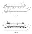
- FIG. 8 shows an example of lateral micro-LEDs.
- the micro-LEDs are lateral micro-LEDs.
- the P electrodes and the N electrodes thereof are located on the same side.
- FIG. 8 shows a red lateral micro-LED 505 , a green lateral micro-LED 506 and a blue lateral micro-LED 507 .
- the red lateral micro-LED 505 contains a P electrode 505 p (positive electrode) and an N electrode 505 n (negative electrode).
- the green lateral micro-LED 506 contains a P electrode 506 p and an N electrode 506 n 6 .
- the blue lateral micro-LED 507 contains a P electrode 507 p and an N electrode 507 n.
- Lead structures (including pads) 515 p , 515 n , 516 p , 516 n , 517 p , 517 n are provided in the substrate 504 .
- the lead structures 515 p , 516 p , 517 p are for connection with positive electrodes.
- the lead structures 515 n , 516 n , 517 n are for connection with negative electrodes.
- the electrodes 505 p , 505 n , 506 p , 506 n , 507 p , 507 n are connected to the lead structures 515 p , 515 n , 516 p , 516 n , 517 p , 517 n via an anisotropic conductive layer 503 .
- Polymer 502 can be coated between the lateral micro-LEDs.
- a transparent cover 501 can be provided over the lateral micro-LEDs.
- FIG. 9 shows another example of lateral micro-LEDs.
- FIG. 9 shows a red lateral micro-LED 605 , a green lateral micro-LED 606 and a blue lateral micro-LED 607 .
- the red lateral micro-LED 605 contains a P electrode 605 p and an N electrode 605 n .
- the green lateral micro-LED 606 contains a P electrode 606 p and an N electrode 606 n .
- the blue lateral micro-LED 607 contains a P electrode 607 p and an N electrode 607 n.
- Lead structures (including pads) 615 p , 615 n , 616 p , 616 n , 617 p , 617 n are provided in the substrate 604 .
- the lead structures 615 p , 616 p , 617 p are for connection with positive electrodes.
- the lead structures 615 n , 616 n , 617 n are for connection with negative electrodes.
- the electrodes 605 p , 605 n , 606 p , 606 n , 607 p , 607 n include solder bumps 602 , for example.
- the solder bumps 602 are coated with flux, for example.
- the electrodes 605 p , 605 n , 606 p , 606 n , 607 p , 607 n are bonded to the lead structures 615 p , 615 n , 616 p , 616 n , 617 p , 617 n , for example, through reflow-soldering, respectively.
- polymer 603 can filled between the lateral micro-LEDs and the substrate 604 .
- a transparent cover 601 can be provided over the lateral micro-LEDs.
- the present invention can further include the specific application of lateral micro-LEDs. More specifically, the present invention further provides a method for transferring micro-LED. The method comprises: forming micro-LEDs on a laser-transparent original substrate, wherein the micro-LEDs are lateral micro-LEDs whose P electrodes and N electrodes are located on one side; bringing the P electrodes and N electrodes of the lateral micro-LEDs into contact with pads preset on a receiving substrate; and irradiating the original substrate with laser from the original substrate side to lift-off the lateral micro-LEDs from the original substrate.
- a technical effect of using lateral micro-LEDs lies in that the processing for N metal electrode after the micro-LED transfer can be omitted. Furthermore, the wafer-level color-binning/testing can be simplified because the P electrodes and N electrodes already exist when a test at wafer-level is performed.
- an anisotropic conductive layer can be provided on a receiving substrate so as to bring the P electrodes and N electrodes of the lateral micro-LEDs into contact with the pads through the anisotropic conductive layer. Then, after lifting-off the lateral micro-LEDs from the original substrate, the anisotropic conductive layer is processed to electrically connect the P electrodes and N electrodes of the lateral micro-LEDs with the pads on the receiving substrate.
- the anisotropic conductive layer can be at least one of an anisotropic conductive film, an anisotropic conductive paste and an anisotropic conductive tape.
- the present invention can further realize the contact by actions of gravity, electrostatic force and/or electromagnetic force.
- the lateral micro-LEDs are separated from the original substrate and the lateral micro-LEDs are dropped off onto the receiving substrate because of gravity.
- electrostatic force can be applied by applying voltage to the pads, so that the lateral micro-LEDs are dropped off onto the receiving substrate after being lifted-off from the original substrate because of the electrostatic force.
- the lateral micro-LEDs contains magnetic substance such as Ni
- a magnetic field can be provided, so that the lateral micro-LEDs are dropped off onto the receiving substrate after being lifted-off from the original substrate because of the electromagnetic force.
- the transfer method in the example of using lateral micro-LEDs can be applied to a method for manufacturing a micro-LED device for transferring the lateral micro-LEDs onto a receiving substrate.
- the receiving substrate is a display screen or display substrate.
- the micro-LED device is a display device, for example.
- a micro-LED device such as a display device
- the micro-LED device adopts lateral micro-LEDs.
- the present invention further provides an electronic apparatus.
- the electronic apparatus contains the micro-LED device.
- the electronic apparatus can be a mobile phone, a pad and so on.
- FIG. 10 shows a flow chart of a method for transferring micro-LEDs by means of a contactless action according to the present invention.
- micro-LEDs are formed on a laser-transparent original substrate.
- the micro-LEDs can be lateral micro-LEDs or can be micro-LEDs of vertical structure.
- the P electrodes and N electrodes thereof are located on one same side.
- the P electrodes and N electrodes thereof are located on opposite sides.
- the original substrate is irradiated with laser from the original substrate side to lift-off the micro-LEDs from the original substrate.
- step S 4300 the micro-LEDs are brought into contact with pads preset on a receiving substrate through an action of contactless action.
- the contactless action means that the action per se can be applied without the direct contact of objects.
- the contactless action can be applied by means of a field. This is different from the action applied through the stickiness of an anisotropic conductive layer or by the surface tension of liquid (such as flux).
- the contactless action per se can be applied without the direct contact of objects, the direct contact of objects can be kept through the contactless action.
- several example of the contactless action are given as below.
- the contactless action is gravity.
- the micro-LEDs are placed over the receiving substrate.
- the micro-LEDs are dropped off on the receiving substrate and is left on the receiving substrate.
- the contactless action is electrostatic force.
- the electrostatic force can be applied by applying voltage to the pads.
- the contactless action is electromagnetic force.
- a magnetic field can be provided by means of a magnet such as permanent magnet, so that the micro-LEDs are dropped off and are left onto the receiving substrate after being lifted-off from the original substrate because of the electromagnetic force, thereby contacting with the pads directly or indirectly.
- the micro-LEDs are attached onto the receiving substrate via a contactless manner, which is not conceived by a person skilled in the art.
- the electrodes of the micro-LEDs include solder bumps.
- the solder bumps are bonded with the pads, for example, through reflow-soldering and so on.
- step S 4200 are shown in front of the step S 4030 , the action of gravity, the action of electrostatic force or the action of electromagnetic force can be applied before the step S 4200 or at the time when performing the step S 4200 .
- the step S 4300 can be performed before the step S 4200 or simultaneously with the step S 4200 .
- the transfer method can be applied to a method for manufacturing a micro-LED device for transferring the micro-LEDs onto a receiving substrate.
- the receiving substrate is a display screen or display substrate.
- the micro-LED device is a display device, for example.
- a micro-LED device such as a display device, can be manufactured by using the manufacturing method.
- the present invention further provides an electronic apparatus.
- the electronic apparatus contains the micro-LED device.
- the electronic apparatus can be a mobile phone, a pad and so on.
Landscapes
- Led Device Packages (AREA)
- Devices For Indicating Variable Information By Combining Individual Elements (AREA)
- Wire Bonding (AREA)
- Container, Conveyance, Adherence, Positioning, Of Wafer (AREA)
Abstract
The present invention discloses a transferring method, a manufacturing method, a device and an electronic apparatus of micro-LED. The method for transferring micro-LED comprises: forming micro-LEDs on a laser-transparent original substrate; irradiating the original substrate with laser from the original substrate side to lift-off the micro-LEDs from the original substrate; bring the micro-LEDs into contact with pads preset on a receiving substrate through a contactless action.
Description
This application is a U.S. national phase under the provisions of 35 U.S.C. § 371 of International Patent Application No. PCT/CN2015/083987 filed Jul. 14, 2015. The disclosure of such international patent application is hereby incorporated herein by reference in its entirety, for all purposes.
The present invention relates to Micro-Light Emitting Diode (micro LED) array for display, and in particular, to a method for transferring micro-LED, a method for manufacturing a micro-LED device, a micro-LED device and an electronic apparatus containing a micro-LED device.
The micro-LED technology refers to the LED array of small size integrated on a substrate with high density. Currently, the micro-LED technology is starting development, and it is expected in the industry that a high-quality micro-LED product comes into the market. High-quality micro-LED will have a deep affection on the conventional display products such as LCD/OLED that have already been put into the market.
In the process of manufacturing micro-LEDs, micro-LEDs are first formed on a donor wafer, and then the micro-LEDs are transferred to a receiving substrate. The receiving substrate is a display screen, for example.
One difficulty during manufacturing a micro-LED lies in how to transfer a micro-LED from a donor wafer to a receiving substrate. In the prior art, the transfer is generally performed by means of electrostatic pick-up. A transfer head array will be needed during the electrostatic pick-up. The structure of the transfer head array is relatively complicated, and the stability thereof shall be considered. An extra cost shall be paid for manufacturing a transfer head array. A phase change shall be made before pick-up with the transfer head array. In addition, during manufacturing with a transfer head array, limitations apply to the thermo budget of a micro-LED for phase change, which is generally lower than 350° C., or more specifically, lower than 200° C.; otherwise, the performance of the micro-LED will be degraded. It generally requires two transfers during the manufacturing with transfer head array, i.e., the transfer from a donor wafer to a carrier wafer and the transfer from the carrier wafer to a receiving substrate.
U.S. Pat. No. 8,333,860B1 discloses an array of transfer heads for transferring micro devices, in which a voltage is applied to the electrode in the transfer head to pick-up a micro device. This patent is fully incorporated hereby as reference herein.
U.S. Pat. No. 8,426,227B1 discloses a method of forming a micro light emitting diode array, in which a micro-LED array is transferred to a receiving substrate by using a transfer head array. This patent is fully incorporated hereby as reference herein.
One object of this invention is to provide a new technical solution for transferring a micro-LED.
According to an embodiment of the present invention, there is provided a method for transferring micro-LED, comprising: forming micro-LEDs on a laser-transparent original substrate; irradiating the original substrate with laser from the original substrate side to lift-off the micro-LEDs from the original substrate; and bring the micro-LEDs into contact with pads preset on a receiving substrate through a contactless action.
Preferably, the contactless action is gravity.
Preferably, the contactless action is electrostatic force. Preferably, the electrostatic force is applied by applying voltage to the pads.
Preferably, the micro-LEDs contain magnetic substance, and the contactless action is electromagnetic force.
Preferably, the electrodes of the micro-LEDs include solder bumps and the method further comprises: bonding the solder bumps with the pads.
Preferably, the micro-LEDs are lateral micro-LEDs or micro-LEDs of vertical structure.
According to another embodiment of the present invention, there is provided a method for manufacturing a micro-LED device, comprising transferring micro-LEDs to a receiving substrate by using the method according to the present invention.
According to another embodiment of the present invention, there is provided a micro-LED device, which is manufactured by using the method according to the present invention.
According to another embodiment of the present invention, there is provided an electronic apparatus, containing a micro-LED device according to the present invention.
In addition, it should be understood by a person skilled in the art that, although a lot of problems exist in the prior art, the solution of each embodiment or each claim could just improve in one or several aspects, and it is not necessary for it to solve all the technical problems listed in the Background of the Invention or in the prior art. It should be understood by a person skilled in the art that content which is not mentioned in a claim should not be regarded as a limitation to said claim.
Further features of the present invention and advantages thereof will become apparent from the following detailed description of exemplary embodiments according to the present invention with reference to the attached drawings.
The accompanying drawings, which are incorporated in and constitute a part of the specification, illustrate embodiments of the invention and, together with the description thereof, serve to explain the principles of the invention.
Various exemplary embodiments of the present invention will now be described in detail with reference to the drawings. It should be noted that the relative arrangement of the components and steps, the numerical expressions, and numerical values set forth in these embodiments do not limit the scope of the present invention unless it is specifically stated otherwise.
The following description of at least one exemplary embodiment is merely illustrative in nature and is in no way intended to limit the invention, its application, or uses.
Techniques, methods and apparatus as known by one of ordinary skill in the relevant art may not be discussed in detail but are intended to be part of the specification where appropriate.
In all of the examples illustrated and discussed herein, any specific values should be interpreted to be illustrative only and non-limiting. Thus, other examples of the exemplary embodiments could have different values.
Notice that similar reference numerals and letters refer to similar items in the following figures, and thus once an item is defined in one figure, it is possible that it need not be further discussed for following figures.
Embodiments and examples of the present invention will be described below with reference to the drawings.
As shown in FIG. 1 , at step S1100, a micro-LED is formed on a laser-transparent original substrate.
The laser-transparent original substrate can be a sapphire substrate, SiC substrate and so on, for example. The micro-LED can be used for being mounted on a display screen panel.
It should be understood by a person skilled in the art that one micro-LED could be formed on the original substrate, or a plurality of micro-LED could be formed on the original substrate. For example, a plurality of micro-LEDs can be formed on the laser-transparent original substrate. The plurality of micro-LEDs can form an array.
In an example, in a case where a plurality of micro-LEDs are formed on the laser-transparent original substrate, the original substrate can be singulated or divided into multiple pieces for more flexible transferring.
At step S1200, the micro-LED is brought into contact with a pad preset on a receiving substrate.
For example, the receiving substrate is a display screen panel.
For example, the pad can be set for red pixel array, yellow pixel array or blue pixel array.
In an example, in a case where a plurality of micro-LED are formed, at least one micro-LED of the plurality of micro-LEDs can be brought into contact with at least one pad preset on the receiving substrate. The at least one micro-LED could be one, several or all of the plurality of micro-LEDs. It should be understood by a person skilled in the art that, although it is just described here that at least one micro-LED, which is expected to be lifted-off, is in contact with a pad, a remaining micro-LED of the plurality of micro-LEDs can also be in contact with a pad.
For example, in the step of contact (S1200), the micro-LED can be brought into contact with the pad preset on the receiving substrate via a liquid thin film. For example, the liquid thin film can include flux. Herein, the lift-off of a micro-LED will be easy through the surface tension force of the liquid thin film (flux), and the successful rate is high.
At step S1300, the original substrate is irradiated with laser from the original substrate side to lift-off the micro-LED from the original substrate.
In an example, in a case where at least one micro-LED is in contact with pad, at least one area on the original substrate can be irradiated with laser from the original substrate side to lift-off the at least one micro-LED from the original substrate. For example, a technician can select the at least one area. For example, the at least one area corresponds to the at least micro-LED, respectively. The at least one area can be just partial area on the original substrate, or can be the whole area.
In another example, the original substrate can be offset for transferring additional micro-LEDs.
In another example, after the transferring using the original substrate, an additional laser-transparent backup substrate can be used to cope with a situation in which micro-LEDs are missing at some points on the display screen panel. For example, a micro-LED can be formed on an additional laser-transparent backup substrate; the micro-LED on the backup substrate is brought into contact with a pad preset on a receiving substrate; and the backup substrate is irradiated with laser from the backup substrate side to lift-off the micro-LED from the backup substrate. In such a way, the quality of a display screen can further be improved.
An array of micro-LEDs can be formed on the receiving substrate after the transferring of micro-LEDs to the receiving substrate.
After the transferring of micro-LEDs to the receiving substrate, the present invention can further include subsequent steps.
For example, the lifted-off micro-LEDs can be reflow-soldered on the receiving substrate. A negative electrode can be deposited on the micro-LEDs. The reflow-soldering can be performed after micro-LEDs of each color are transferred. Alternatively, the reflow-soldering can be performed after micro-LEDs of all colors are transferred.
In addition, the soldered micro-LED can be filled with polymer. For example, a confocal dielectric deposition can be used in stead of polymer filling.
In another embodiment, the present invention further includes a method for manufacturing a micro-LED device. The manufacturing method comprises transferring a micro-LED to a receiving substrate by using the method for transferring a micro-LED according to the present invention.
In another embodiment, the present invention further includes a micro-LED device, such as a display screen device. The micro-LED device can be manufactured by using the method for manufacturing a micro-LED device according to the present invention.
In comparison with the prior art, under the similar conditions, the micro-LED manufactured by using the solution of the present invention is relatively simple and reliable while maintaining a high quality, and the through put thereof is relatively high with low cost.
In another embodiment, the present invention further includes an electronic apparatus. The electronic apparatus contains a micro-LED device according to the present invention. For example, the electronic apparatus can be a mobile phone, a pad computer and so on.
In the solution of the present invention, a micro-LED is formed directly on the original substrate and it is transferred to a receiving substrate by means of laser lift-off. The solution of this invention have not been conceived by the prior art.
In addition, the micro-LED can be selectively transferred through the present invention.
In addition, in the solution of the present invention, the transfer can be performed only once while two transfers are needed in the prior art.
In addition, in comparison with the prior art, the solution of the present invention is relatively efficient, the cost is relatively low and product performance degrade due to an extra thermal budget will not occur.
In addition, in comparison with the prior art using a pick-up head, the present invention does not need a complicated pick-up system, and thus the cost of product manufactured using the present invention will relatively low and reliable.
In addition, since it does not need the temporary bonding in the prior art between the micro-LED and the intermediate carrier substrate, the cost can be further decreased by this invention.
Since it is not necessary to consider the phase change of bonding layer considered in the prior art using pick-up head, the manufacturing method of the present invention can have a relatively high through put and the extra thermal load limitation will be less. Consequently, under the similar conditions, the manufactured micro-LED will have a higher performance
An example for transferring a micro-LED according to the present invention will be described below with reference to FIGS. 2A to 2G .
As shown in FIG. 2A , micro-LEDs 2 are formed on a laser-transparent original substrate 1 such as sapphire substrate. The micro-LEDs 2 have a vertical micro-LED structure, for example. The micro-LEDs 2 contains, for example, a n-doped GaN layer, a multiple quantum well structure, a p-doped GaN layer, a p metal electrode, a bump, and so on.
As shown in FIG. 2A , the plurality of micro-LEDs 2 can be singulated.
As shown in FIG. 2B , the original substrate 1 is flipped over, and is aligned with a receiving substrate 4 with liquid thin film (for example, containing flux) 5. The micro bumps on the micro-LEDs are in contact with the flux. Pads 3 are preset on the receiving substrate 4. For example, the pads 3 include pad 3 r for receiving red micro-LED, pad 3 b for receiving blue micro-LED and pad 3 g for receiving green micro-LED.
As shown in FIG. 2C , partial areas 7 on the original substrate are selectively irradiated with laser 6, to lift off the selected micro-LEDs 2 a, 2 b of the plurality of formed micro-LEDs from the original substrate.
As shown in FIG. 2D , the original substrate 1 is lifted up. Because of the function of the surface tension force of the liquid thin film, the selected micro-LEDs 2 a, 2 b are lifted-off easily, while the other micro-LEDs are remained on the original substrate 1.
Then, the original substrate is moved and the operations of FIGS. 2C to 2D are repeated, so that a plurality of micro-LEDs are transferred to the receiving substrate.
As shown in FIG. 2E , the plurality of micro-LEDs are transferred to the receiving substrate 4.
As shown in FIG. 2F , for example, the plurality of micro-LEDs are soldered onto the receiving substrate through reflow soldering. Then, the flux is cleaned.
As shown in FIG. 2G , the receiving substrate is filled with polymer 8 and is sealed. Then, n-metal electrode 9 is deposited, for example, using ITO material.
As shown in FIG. 3 , at step S2100, micro-LEDs are formed on a laser-transparent original substrate.
At step S2200, an anisotropic conductive layer is provided on a receiving substrate.
For example, the anisotropic conductive layer is at least one of an anisotropic conductive film (ACF), an anisotropic conductive paste (ACP) and an anisotropic conductive tape (ACT).
At step S2300, the micro-LEDs are brought into contact with the anisotropic conductive layer on the receiving substrate. For example, the micro-LEDs are adhered to the anisotropic conductive layer on the receiving substrate. At this step, the micro-LEDs can be aligned with the receiving substrate in advance, for example.
At step S2400, the original substrate is irradiated with laser from the original substrate side to lift-off the micro-LEDs from the original substrate.
For example, the above steps can be performed with respect to red micro-LEDs, green micro-LEDs and blue micro-LEDs, respectively. Since the transfer with respect to the three micro-LEDs can be regarded as a simple repeat of the above steps, they are not repeated here. As long as each of the above steps are performed in a solution, the solution will be covered by this invention.
At step S2500, the anisotropic conductive layer is processed to electrically connect the micro-LEDs (its electrodes) with the pads on the receiving substrate.
In an example, pressure can be applied on the anisotropic conductive layer from the micro-LED side by using an auxiliary substrate. For example, the temperature of processing the anisotropic conductive layer can be between 150° C. and 200° C. For example, the applied pressure is between 1 MPa and 4 MPa. For example, the time period of applying pressure is between 10 second and 30 second.
In an example, the auxiliary substrate can be a flat rigid substrate. The inventors of the present application have found that the possible displacement of the micro-LEDs can be reduced by using a rigid substrate. This point has not noticed by a person skilled in the art.
For example, the surface of the auxiliary substrate can be coated with temporary bonding polymer. In this situation, the step S2500 can further comprises: bonding the auxiliary substrate with the anisotropic conductive layer via the temporary bonding polymer; and after applying pressure, de-bonding the auxiliary substrate via the temporary bonding polymer, to remove the auxiliary substrate. The advantage of temporarily bonding the auxiliary substrate with the anisotropic conductive layer lies in that, the positions of the micro-LEDs can be relatively fixed, and the displacement of micro-LEDs during processing the anisotropic conductive layer is reduced.
After the above processes, normal subsequent processes can be done on the micro-LEDs. For example, the subsequent processes include: etching the temporary bonding polymer, to expose the epitaxial layers of the micro-LEDs; forming N-metal electrodes on the epitaxial layers of the micro-LEDs; and performing encapsulation on the N-metal electrodes.
For example, the receiving substrate can be a display substrate. Leads and pads can be set on the receiving substrate in advance, to be electronically connect with the micro-LEDs.
In this embodiment, the micro-LEDs and the receiving substrate are connected through a anisotropic conductive layer. This approach of processing is relatively simple and is more suitable for production in large bulk.
In another embodiment, the present invention further provides a method for manufacturing a micro-LED device. The manufacturing method comprises transferring micro-LEDs to a receiving substrate by using the method according to the present invention. For example, the receiving substrate is a display screen or display substrate. The micro-LED device is a display device, for example.
In another embodiment, the present invention further provides a micro-LED device, such as a display device. The micro-LED device can be manufactured by using the method for manufacturing a micro-LED device according to the present invention. In the micro-LED device according to the embodiment, the micro-LEDs come into electronic contact with the pads on the receiving substrate via the anisotropic conductive layer, which is different from the micro-LED device in the prior art.
In another embodiment, the present invention further provides an electronic apparatus. The electronic apparatus contains a micro-LED device according to the embodiment. For example, the electronic apparatus can be a mobile phone, a pad and so on.
As shown in FIG. 4A , an original substrate 201 such as a sapphire substrate has red micro-LEDs 202 thereon. The receiving substrate 204 such as display substrate has an anisotropic conductive film (ACF) 203 thereon. The receiving substrate 204 has signal leads 205 and pads 205′ for connecting micro-LEDs.
As shown in FIG. 4B , the original substrate 201 (red micro-LED 202) is brought into contact with the anisotropic conductive film 203 with a light force. For example, the red micro-LEDs 202 to be transferred can be aligned with the pads on the receiving substrate 204. The original substrate 201 is irradiated with laser 206, to selectively lift-off red micro-LEDs.
After the transfer of micro-LEDs in the three colors, an inspection and repair can be performed with respect to any defect.
In FIG. 4K , the ACF 203 is processed through the auxiliary substrate 213. For example, the processing condition is that the temperature is be between 150° C. and 200° C., the applied pressure is between 1 MPa and 4 MPa, the time period of applying pressure is between 10 second and 30 second. Through these processes, the ACF 203 interconnects the micro-LEDs with corresponding pad in the vertical direction.
Then, the auxiliary substrate 213 is de-bonded (through the polymer 214).
In FIG. 4L , the normal subsequent processes are performed: etching the polymer 214, to expose the epitaxial layers of the micro-LEDs; forming N-metal electrodes 215 (for example, ITO electrodes) on the epitaxial layers of the micro-LEDs; and performing encapsulation 216 on the N-metal electrodes (for example, PET lamination).
As shown in FIG. 5 , at step S3100, at least one micro-LED is transferred from an original substrate to a support body. For example, the original substrate is laser-transparent.
In an example, this step can comprises: mounting the original substrate onto the support body, wherein the micro-LEDs are formed on the original substrate, the support body has light-release adhesive on its surface, and the micro-LEDs are adhered to the support body via the light-release adhesive; irradiating the original substrate with laser from the original substrate side, for lifting-off the at least one micro-LED from the original substrate, and irradiating light from the support body side, to release un-lifted-off micro-LEDs. In this example, the support body is transparent.
For example, the light-release adhesive can be a UV tape. For example, the support body is stiff. The displacement of micro-LEDs during transfer will have affect on the quality of the final product. The inventors of this application have found that this displacement can be reduced by using a stiff support body. This point has not been noticed by a person skilled in the art. For example, the material of the support body can be PET.
Generally, it is difficult to form red micro-LEDs on a laser-transparent substrate such as a sapphire substrate. Accordingly, in an example, the red micro-LEDs are formed in advance and then are transferred to an original substrate, for being finally transferred to a receiving substrate. For example, in this embodiment, red micro-LEDs can be formed on a growth substrate. Then, the red micro-LEDs are transferred to an intermediate substrate. After that, the red micro-LEDs are transferred from the intermediate substrate to the original substrate.
At step S3200, the at least one micro-LED are transferred from the support body to a backup substrate.
For example, the backup substrate has elastomer or polymer on its surface. For example, the at least one micro-LED are bonded to the backup substrate through the elastomer or polymer.
In an example, this step can further comprises: bonding the support body with the at least one micro-LED to the backup substrate, and irradiating light from the support body side, to release the at least one micro-LED.
At step S3300, the at least one micro-LED are transferred from the backup substrate to a receiving substrate.
In an example, the step can further comprise: aligning the at least one micro-LED with the pads on the receiving substrate; and lifting-off the at least one micro-LED via the elastomer or polymer.
For example, the above transfer steps can be performed with respect to red micro-LEDs, blue micro-LEDs and greed micro-LEDs, respectively. They will not be repeatedly described here.
After the above processes, normal subsequent processes can be done on the micro-LEDs. For example, the subsequent processes include: coating polymer on the receiving substrate with micro-LEDs; curing the polymer; etching the polymer, to expose the epitaxial layers of the micro-LEDs; forming N-metal electrodes on the epitaxial layers of the micro-LEDs; and performing encapsulation on the N-metal electrodes.
The inventors of this invention have found that during the transfer of micro-LEDs, usually, only part of the micro-LEDs on the original substrate are transferred. If the micro-LEDs are directly transferred to a receiving substrate, the remaining micro-LEDs on the original substrate are often contaminated. In this embodiment, this contamination can reduced through the transfer via an intermediate support body.
In another embodiment, the present invention further provides a method for manufacturing a micro-LED device. The manufacturing method comprises transferring micro-LEDs to a receiving substrate by using the method for transferring micro-LEDs according to this embodiment. For example, the receiving substrate is a display screen or display substrate. The micro-LED device is a display device, for example.
In another embodiment, the present invention further provides a micro-LED device, such as a display device. The micro-LED device can be manufactured by using the method for manufacturing a micro-LED device according to said embodiment.
In another embodiment, the present invention further provides an electronic apparatus. The electronic apparatus contains a micro-LED device according to the embodiment. For example, the electronic apparatus can be a mobile phone, a pad and so on.
Generally, red micro-LEDs cannot be directly formed on a laser-transparent original substrate such as sapphire substrate. Thus, it is required that red micro-LEDs are formed on an additional substrate in advance, and then are transferred to a sapphire substrate. FIG. 6A to 6F shows an example for transferring red micro-LEDs according to the present invention.
As shown in FIG. 6A , red micro-LEDs 302 are formed on a growth substrate 301 such as GaAs substrate.
As shown in FIG. 6B , the red micro-LEDs 302 are bonded with intermediate substrate 304 such as silicon substrate, through temporary bonding polymer 303. The polymer 303 is a thermal release tape (TRT), for example.
As shown in FIG. 6C , the growth substrate 301 is removed by a wet etching method, for example.
As shown in FIG. 6D , a light resist 305 is coated on an original substrate 306 such as sapphire substrate. The original substrate 306 and the red micro-LEDs 302 are bonded through the resist 305. The resist 305 can endure the temperature above 200° C.; generally above 250° C.
As shown in FIG. 6E , the polymer 303 is processed under a temperature less than 200° C., to remove the intermediate substrate 304.
As shown in FIG. 6F , a O2 plasma etching is performed on the resist 305, to isolate the respective red micro-LEDs 302.
As shown in FIG. 7A , the original substrate 406 has resist 405 and red micro-LEDs 402 thereon. The red micro-LEDs 402 are mounted onto a UV tape 411. The UV tape 411 is located on a stiff PET support body 402. The red micro-LEDs are selectively lifted-off through laser 413.
As shown in FIG. 7B , a ultraviolet is irradiated from the support body 412 side, to release un-lifted-off red micro-LEDs.
The lifted-off red micro-LEDs 402 r are easily separated from the original substrate 406. As shown in FIG. 7C , the lifted-off red micro-LEDs 402 r are adhered on the UV tape 411, while other red micro-LEDs remain on the original substrate 406.
As shown in FIG. 7D , the backup substrate 415 such as glass substrate has elastomer/polymer 416 thereon. For example, the elastomer/polymer 416 is coated on the backup substrate 415 through spin coating. For example, the elastomer/polymer 416 is PDMS or 3M LC 5320, and can be cured through ultraviolet, for example.
As shown in FIG. 7E , the support body is fully irradiated with ultraviolet, to release the red micro-LEDs and elastomer/polymer 416.
After that, for example, if the micro-LEDs do not have bumps thereon, the micro-LEDs on the backup substrate 415 can be screen-printed using silver paste.
As shown in 7F, the red micro-LEDs on the backup substrate 415 are aligned with the pads 419 on the receiving substrate 417. For example, the receiving substrate is a display substrate, and includes signal leads 418. For example, the red micro-LEDs are bonded to the pads 419 through reflow. The temperature of reflow can be more than 260° C. Then, the backup substrate 415 is separated from the receiving substrate 417 through laser lift-off.
In FIG. 7L , the normal subsequent processes are performed on the transferred micro-LEDs: coating polymer 426 on the receiving substrate with micro-LEDs; curing the polymer 426; etching the polymer, to expose the epitaxial layers of the micro-LEDs; forming N-metal electrodes 427 on the epitaxial layers of the micro-LEDs; and performing encapsulation (not shown) on the N-metal electrodes.
The solution of the present invention can use both vertical micro-LEDs and lateral micro-LEDs (flip-chip micro-LEDs). The micro-LEDs of vertical structure shown in the previous figures are illustrative and do not limit the scope of the present invention. FIG. 8 shows an example of lateral micro-LEDs.
In the example of FIG. 8 , the micro-LEDs are lateral micro-LEDs. In the lateral micro-LEDs, the P electrodes and the N electrodes thereof are located on the same side. FIG. 8 shows a red lateral micro-LED 505, a green lateral micro-LED 506 and a blue lateral micro-LED 507. The red lateral micro-LED 505 contains a P electrode 505 p (positive electrode) and an N electrode 505 n (negative electrode). The green lateral micro-LED 506 contains a P electrode 506 p and an N electrode 506 n 6. The blue lateral micro-LED 507 contains a P electrode 507 p and an N electrode 507 n.
Lead structures (including pads) 515 p, 515 n, 516 p, 516 n, 517 p, 517 n are provided in the substrate 504. The lead structures 515 p, 516 p, 517 p are for connection with positive electrodes. The lead structures 515 n, 516 n, 517 n are for connection with negative electrodes.
In the example of FIG. 8 , the electrodes 505 p, 505 n, 506 p, 506 n, 507 p, 507 n are connected to the lead structures 515 p, 515 n, 516 p, 516 n, 517 p, 517 n via an anisotropic conductive layer 503.
Polymer 502 can be coated between the lateral micro-LEDs. A transparent cover 501 can be provided over the lateral micro-LEDs.
Lead structures (including pads) 615 p, 615 n, 616 p, 616 n, 617 p, 617 n are provided in the substrate 604. The lead structures 615 p, 616 p, 617 p are for connection with positive electrodes. The lead structures 615 n, 616 n, 617 n are for connection with negative electrodes.
In the example of FIG. 9 , the electrodes 605 p, 605 n, 606 p, 606 n, 607 p, 607 n include solder bumps 602, for example. The solder bumps 602 are coated with flux, for example. The electrodes 605 p, 605 n, 606 p, 606 n, 607 p, 607 n are bonded to the lead structures 615 p, 615 n, 616 p, 616 n, 617 p, 617 n, for example, through reflow-soldering, respectively.
For example, polymer 603 can filled between the lateral micro-LEDs and the substrate 604. A transparent cover 601 can be provided over the lateral micro-LEDs. These processes are well-known in the art and thus are not described in detail here.
Therefore, for example, the present invention can further include the specific application of lateral micro-LEDs. More specifically, the present invention further provides a method for transferring micro-LED. The method comprises: forming micro-LEDs on a laser-transparent original substrate, wherein the micro-LEDs are lateral micro-LEDs whose P electrodes and N electrodes are located on one side; bringing the P electrodes and N electrodes of the lateral micro-LEDs into contact with pads preset on a receiving substrate; and irradiating the original substrate with laser from the original substrate side to lift-off the lateral micro-LEDs from the original substrate.
A technical effect of using lateral micro-LEDs lies in that the processing for N metal electrode after the micro-LED transfer can be omitted. Furthermore, the wafer-level color-binning/testing can be simplified because the P electrodes and N electrodes already exist when a test at wafer-level is performed.
Furthermore, for example, in this method, an anisotropic conductive layer can be provided on a receiving substrate so as to bring the P electrodes and N electrodes of the lateral micro-LEDs into contact with the pads through the anisotropic conductive layer. Then, after lifting-off the lateral micro-LEDs from the original substrate, the anisotropic conductive layer is processed to electrically connect the P electrodes and N electrodes of the lateral micro-LEDs with the pads on the receiving substrate.
For example, the anisotropic conductive layer can be at least one of an anisotropic conductive film, an anisotropic conductive paste and an anisotropic conductive tape.
In addition to bringing the P electrodes and N electrodes of the lateral micro-LEDs into contact with pads preset on a receiving substrate by the stickiness of an anisotropic conductive layer or by the surface tension of liquid (such as flux), the present invention can further realize the contact by actions of gravity, electrostatic force and/or electromagnetic force.
For example, when the original substrate is irradiated with laser from the original substrate side, the lateral micro-LEDs are separated from the original substrate and the lateral micro-LEDs are dropped off onto the receiving substrate because of gravity.
For example, electrostatic force can be applied by applying voltage to the pads, so that the lateral micro-LEDs are dropped off onto the receiving substrate after being lifted-off from the original substrate because of the electrostatic force.
For example, in case that the lateral micro-LEDs contains magnetic substance such as Ni, a magnetic field can be provided, so that the lateral micro-LEDs are dropped off onto the receiving substrate after being lifted-off from the original substrate because of the electromagnetic force.
Similarly, the transfer method in the example of using lateral micro-LEDs can be applied to a method for manufacturing a micro-LED device for transferring the lateral micro-LEDs onto a receiving substrate. For example, the receiving substrate is a display screen or display substrate. The micro-LED device is a display device, for example.
For example, a micro-LED device, such as a display device, can be manufactured by using the manufacturing method. The micro-LED device adopts lateral micro-LEDs.
For example, the present invention further provides an electronic apparatus. The electronic apparatus contains the micro-LED device. For example, the electronic apparatus can be a mobile phone, a pad and so on.
As shown in FIG. 10 , in the method for transferring micro-LEDs, at step S4100, micro-LEDs are formed on a laser-transparent original substrate.
The micro-LEDs can be lateral micro-LEDs or can be micro-LEDs of vertical structure. In a lateral micro-LED, the P electrodes and N electrodes thereof are located on one same side. In a micro-LED of vertical structure, the P electrodes and N electrodes thereof are located on opposite sides.
At step S4200, the original substrate is irradiated with laser from the original substrate side to lift-off the micro-LEDs from the original substrate.
At step S4300, the micro-LEDs are brought into contact with pads preset on a receiving substrate through an action of contactless action.
The contactless action means that the action per se can be applied without the direct contact of objects. For example, the contactless action can be applied by means of a field. This is different from the action applied through the stickiness of an anisotropic conductive layer or by the surface tension of liquid (such as flux). It should be understand that although the contactless action per se can be applied without the direct contact of objects, the direct contact of objects can be kept through the contactless action. For example, several example of the contactless action are given as below.
For example, the contactless action is gravity. The micro-LEDs are placed over the receiving substrate. When the lift-off is performed, the micro-LEDs are dropped off on the receiving substrate and is left on the receiving substrate.
For example, the contactless action is electrostatic force. The electrostatic force can be applied by applying voltage to the pads.
For example, the contactless action is electromagnetic force. In case that the micro-LEDs contain magnetic substance, a magnetic field can be provided by means of a magnet such as permanent magnet, so that the micro-LEDs are dropped off and are left onto the receiving substrate after being lifted-off from the original substrate because of the electromagnetic force, thereby contacting with the pads directly or indirectly.
In this embodiment, the micro-LEDs are attached onto the receiving substrate via a contactless manner, which is not conceived by a person skilled in the art.
For example, the electrodes of the micro-LEDs include solder bumps. The solder bumps are bonded with the pads, for example, through reflow-soldering and so on.
The order of steps in FIG. 10 will not constitute any limitation o the present invention. For example, although the step S4200 are shown in front of the step S4030, the action of gravity, the action of electrostatic force or the action of electromagnetic force can be applied before the step S4200 or at the time when performing the step S4200. In another word, for example, the step S4300 can be performed before the step S4200 or simultaneously with the step S4200.
Similarly, the transfer method can be applied to a method for manufacturing a micro-LED device for transferring the micro-LEDs onto a receiving substrate. For example, the receiving substrate is a display screen or display substrate. The micro-LED device is a display device, for example.
For example, a micro-LED device, such as a display device, can be manufactured by using the manufacturing method.
For example, the present invention further provides an electronic apparatus. The electronic apparatus contains the micro-LED device. For example, the electronic apparatus can be a mobile phone, a pad and so on.
Although some specific embodiments of the present invention have been demonstrated in detail with examples, it should be understood by a person skilled in the art that the above examples are only intended to be illustrative but not to limit the scope of the present invention. It should be understood by a person skilled in the art that the above embodiments can be modified without departing from the scope and spirit of the present invention. The scope of the present invention is defined by the attached claims.
Claims (7)
1. A method for transferring micro Light-Emitting Diodes (micro-LEDs), comprising:
forming micro-LEDs on a laser-transparent original substrate;
irradiating the laser-transparent original substrate with laser from a laser-transparent original substrate side to lift-off the micro-LEDs from the laser-transparent original substrate; and
bringing the micro-LEDs into contact with pads preset on a receiving substrate through an action of electrostatic force applied by applying voltage to the pads, so that the micro-LEDs are dropped off onto the receiving substrate after being lifted-off from the laser-transparent original substrate.
2. The method according to claim 1 , wherein said bringing the micro-LEDs into contact with pads preset on the receiving substrate is assisted by gravity.
3. The method according to claim 1 , wherein the micro-LEDs contain magnetic substance, and said bringing the micro-LEDs into contact with pads preset on the receiving substrate is assisted by electromagnetic force.
4. The method according to claim 1 , wherein electrodes of the micro-LEDs include solder bumps and the method further comprises: bonding the solder bumps with the pads.
5. The method according to claim 1 , wherein the micro-LEDs are lateral micro-LEDs or micro-LEDs of vertical structure.
6. A method for manufacturing a micro-LED device, comprising transferring a micro-LED to a receiving substrate by using the method according to claim 1 .
7. A micro-LED device, which is manufactured by using the method according to claim 6 .
Applications Claiming Priority (1)
| Application Number | Priority Date | Filing Date | Title |
|---|---|---|---|
| PCT/CN2015/083987 WO2017008253A1 (en) | 2015-07-14 | 2015-07-14 | Transferring method, manufacturing method, device and electronic apparatus of micro-led |
Publications (2)
| Publication Number | Publication Date |
|---|---|
| US20170330857A1 US20170330857A1 (en) | 2017-11-16 |
| US10224308B2 true US10224308B2 (en) | 2019-03-05 |
Family
ID=57756660
Family Applications (1)
| Application Number | Title | Priority Date | Filing Date |
|---|---|---|---|
| US15/531,270 Active US10224308B2 (en) | 2015-07-14 | 2015-07-14 | Transferring method, manufacturing method, device and electronic apparatus of micro-LED |
Country Status (5)
| Country | Link |
|---|---|
| US (1) | US10224308B2 (en) |
| EP (1) | EP3323145A1 (en) |
| JP (1) | JP2018503986A (en) |
| CN (1) | CN107924866B (en) |
| WO (1) | WO2017008253A1 (en) |
Cited By (2)
| Publication number | Priority date | Publication date | Assignee | Title |
|---|---|---|---|---|
| US20220140181A1 (en) * | 2020-11-04 | 2022-05-05 | Coretronic Corporation | Bonding method for electronic element |
| US12356767B2 (en) | 2020-02-13 | 2025-07-08 | Samsung Display Co., Ltd. | Display device |
Families Citing this family (33)
| Publication number | Priority date | Publication date | Assignee | Title |
|---|---|---|---|---|
| US9633883B2 (en) | 2015-03-20 | 2017-04-25 | Rohinni, LLC | Apparatus for transfer of semiconductor devices |
| CN105870265A (en) * | 2016-04-19 | 2016-08-17 | 京东方科技集团股份有限公司 | Light-emitting diode substrate and preparation method thereof and display device |
| US10141215B2 (en) | 2016-11-03 | 2018-11-27 | Rohinni, LLC | Compliant needle for direct transfer of semiconductor devices |
| US10504767B2 (en) | 2016-11-23 | 2019-12-10 | Rohinni, LLC | Direct transfer apparatus for a pattern array of semiconductor device die |
| US10471545B2 (en) | 2016-11-23 | 2019-11-12 | Rohinni, LLC | Top-side laser for direct transfer of semiconductor devices |
| US10062588B2 (en) | 2017-01-18 | 2018-08-28 | Rohinni, LLC | Flexible support substrate for transfer of semiconductor devices |
| TWI756384B (en) * | 2017-03-16 | 2022-03-01 | 美商康寧公司 | Method and process for mass transfer of micro-leds |
| JP6985031B2 (en) * | 2017-05-19 | 2021-12-22 | 株式会社ディスコ | Manufacturing method of LED display panel |
| JP2019015899A (en) * | 2017-07-10 | 2019-01-31 | 株式会社ブイ・テクノロジー | Display device manufacturing method, chip component transferring method, and transferring member |
| KR101956231B1 (en) * | 2017-11-20 | 2019-03-08 | 엘지디스플레이 주식회사 | Display device and method of manufacturing the same |
| TWI637481B (en) | 2017-11-29 | 2018-10-01 | 財團法人工業技術研究院 | Semiconductor structure, light emitting device and method of manufacturing same |
| JP7140315B2 (en) * | 2018-03-14 | 2022-09-21 | 京東方科技集團股▲ふん▼有限公司 | A method for transferring multiple micro-light emitting diodes onto a target substrate |
| US10410905B1 (en) | 2018-05-12 | 2019-09-10 | Rohinni, LLC | Method and apparatus for direct transfer of multiple semiconductor devices |
| CN108962042B (en) * | 2018-07-23 | 2021-04-02 | 上海天马微电子有限公司 | Display panel and method of making the same |
| EP3844078B1 (en) | 2018-08-31 | 2025-03-19 | Dow Global Technologies LLC | Polypropylene laminate sheet |
| US11094571B2 (en) | 2018-09-28 | 2021-08-17 | Rohinni, LLC | Apparatus to increase transferspeed of semiconductor devices with micro-adjustment |
| CN109216400B (en) * | 2018-10-29 | 2020-11-24 | 厦门乾照光电股份有限公司 | Mass transfer device and related method for Micro LED array devices |
| CN111292631B (en) * | 2018-11-21 | 2022-03-25 | 成都辰显光电有限公司 | Micro light-emitting diode display panel and preparation method thereof |
| DE102018132824B4 (en) | 2018-12-19 | 2024-10-10 | OSRAM Opto Semiconductors Gesellschaft mit beschränkter Haftung | METHOD FOR PRODUCING AN OPTOELECTRONIC LIGHTING DEVICE |
| CN109887867B (en) * | 2019-03-08 | 2021-03-09 | 京东方科技集团股份有限公司 | Micro device transfer device and micro device transfer method |
| CN110581216B (en) * | 2019-08-02 | 2021-08-31 | 潍坊歌尔微电子有限公司 | Manufacturing method of magnetic sensor, magnetic sensor and electronic device |
| KR20210019323A (en) * | 2019-08-12 | 2021-02-22 | 삼성전자주식회사 | Micro led display and manufacturing method thereof |
| KR20210051039A (en) * | 2019-10-29 | 2021-05-10 | 엘지디스플레이 주식회사 | Donor and transfer method using the same |
| CN111834262B (en) * | 2020-07-24 | 2023-08-08 | 錼创显示科技股份有限公司 | Microelectronic element transfer device and microelectronic element transfer method |
| TWI761895B (en) | 2020-07-24 | 2022-04-21 | 錼創顯示科技股份有限公司 | Micro-electron element transfer apparatus and micro-electron element transfer method |
| CN112310252B (en) * | 2020-10-16 | 2022-02-22 | 深圳市华星光电半导体显示技术有限公司 | Micro LED crystal grain, Micro LED substrate and preparation method thereof |
| TW202316644A (en) * | 2021-02-22 | 2023-04-16 | 加拿大商弗瑞爾公司 | Backplane pad |
| KR20230147717A (en) * | 2021-02-22 | 2023-10-23 | 뷰리얼 인크. | cartridge interference |
| US20220320366A1 (en) * | 2021-03-31 | 2022-10-06 | Semileds Corporation | Method To Remove An Isolation Layer On The Corner Between The Semiconductor Light Emitting Device To The Growth Substrate |
| JP7580890B2 (en) * | 2021-04-16 | 2024-11-12 | 株式会社ディスコ | Manufacturing method of LED display panel |
| TWI766699B (en) * | 2021-05-25 | 2022-06-01 | 台灣愛司帝科技股份有限公司 | Method for transferring electronic elements |
| US20250374725A1 (en) * | 2022-05-31 | 2025-12-04 | Lg Electronics Inc. | Display device using light emitting elements and manufacturing method therefor |
| WO2024247248A1 (en) * | 2023-06-02 | 2024-12-05 | 東北マイクロテック株式会社 | Microelement, arraying system, and mounting method |
Citations (7)
| Publication number | Priority date | Publication date | Assignee | Title |
|---|---|---|---|---|
| CN102754185A (en) | 2009-12-11 | 2012-10-24 | 夏普株式会社 | Method for manufacturing semiconductor device, and semiconductor device |
| US8333860B1 (en) | 2011-11-18 | 2012-12-18 | LuxVue Technology Corporation | Method of transferring a micro device |
| US8426227B1 (en) | 2011-11-18 | 2013-04-23 | LuxVue Technology Corporation | Method of forming a micro light emitting diode array |
| US20140094878A1 (en) | 2012-10-01 | 2014-04-03 | Albert-Ludwigs-Universitat Freiburg | Method for producing a micro-led matrix, micro-led matrix and use of a micro-led matrix |
| CN104465474A (en) | 2014-11-14 | 2015-03-25 | 昆山工研院新型平板显示技术中心有限公司 | Displaying device transfer-print locating device and method |
| US20160204313A1 (en) * | 2013-09-26 | 2016-07-14 | Dexerials Corporation | Light-emitting device, anisotropic conductive paste, and method of manufacturing light-emitting device |
| US20160300745A1 (en) * | 2015-04-07 | 2016-10-13 | Lg Electronics Inc. | Semiconductor light emitting device, transfer head of semiconductor light emitting device, and method of transferring semiconductor light emitting device |
Family Cites Families (8)
| Publication number | Priority date | Publication date | Assignee | Title |
|---|---|---|---|---|
| JP2001237266A (en) * | 2000-02-23 | 2001-08-31 | Sony Corp | Semiconductor chip and mounting method thereof |
| JP2001257218A (en) * | 2000-03-10 | 2001-09-21 | Sony Corp | Method for mounting fine chip |
| US7251882B2 (en) * | 2004-09-03 | 2007-08-07 | Eastman Kodak Company | Method for assembling micro-components to binding sites |
| US7943052B2 (en) * | 2005-07-05 | 2011-05-17 | National Taiwan University | Method for self-assembling microstructures |
| JP5444798B2 (en) * | 2009-04-10 | 2014-03-19 | ソニー株式会社 | Device transfer method |
| CN102130285B (en) * | 2010-11-03 | 2012-12-26 | 映瑞光电科技(上海)有限公司 | Light emitting diode and manufacturing method thereof |
| JP6404567B2 (en) * | 2013-12-26 | 2018-10-10 | シャープ株式会社 | LIGHT EMITTING ELEMENT, LIGHT EMITTING DEVICE MANUFACTURING METHOD, LIGHT EMITTING DEVICE HAVING MULTIPLE LIGHT EMITTING ELEMENT, AND LIGHT EMITTING DEVICE MANUFACTURING METHOD |
| US20170047495A1 (en) * | 2015-08-11 | 2017-02-16 | Sensor Electronic Technology, Inc. | Optoelectronic Semiconductor Device With Ferromagnetic Domains |
-
2015
- 2015-07-14 US US15/531,270 patent/US10224308B2/en active Active
- 2015-07-14 JP JP2017547034A patent/JP2018503986A/en active Pending
- 2015-07-14 EP EP15897981.5A patent/EP3323145A1/en not_active Ceased
- 2015-07-14 WO PCT/CN2015/083987 patent/WO2017008253A1/en not_active Ceased
- 2015-07-14 CN CN201580001235.5A patent/CN107924866B/en active Active
Patent Citations (7)
| Publication number | Priority date | Publication date | Assignee | Title |
|---|---|---|---|---|
| CN102754185A (en) | 2009-12-11 | 2012-10-24 | 夏普株式会社 | Method for manufacturing semiconductor device, and semiconductor device |
| US8333860B1 (en) | 2011-11-18 | 2012-12-18 | LuxVue Technology Corporation | Method of transferring a micro device |
| US8426227B1 (en) | 2011-11-18 | 2013-04-23 | LuxVue Technology Corporation | Method of forming a micro light emitting diode array |
| US20140094878A1 (en) | 2012-10-01 | 2014-04-03 | Albert-Ludwigs-Universitat Freiburg | Method for producing a micro-led matrix, micro-led matrix and use of a micro-led matrix |
| US20160204313A1 (en) * | 2013-09-26 | 2016-07-14 | Dexerials Corporation | Light-emitting device, anisotropic conductive paste, and method of manufacturing light-emitting device |
| CN104465474A (en) | 2014-11-14 | 2015-03-25 | 昆山工研院新型平板显示技术中心有限公司 | Displaying device transfer-print locating device and method |
| US20160300745A1 (en) * | 2015-04-07 | 2016-10-13 | Lg Electronics Inc. | Semiconductor light emitting device, transfer head of semiconductor light emitting device, and method of transferring semiconductor light emitting device |
Non-Patent Citations (3)
| Title |
|---|
| Marinov, V., et al., "Laser-Enabled Advanced Packaging of Ultrathin Bare Dice in Flexible Substrates", "IEEE Transactions on Components, Packaging and Manufacturing Technology", Apr. 30, 2012, pp. 569-577, vol. 2, No. 4. |
| Mathews, S., et al., "Manufacturing Microelectronics Using 'Lase-and-Place'", "Photonics Spectra", Oct. 31, 2007, pp. 70-74, vol. 41, No. 10. |
| Mathews, S., et al., "Manufacturing Microelectronics Using ‘Lase-and-Place’", "Photonics Spectra", Oct. 31, 2007, pp. 70-74, vol. 41, No. 10. |
Cited By (3)
| Publication number | Priority date | Publication date | Assignee | Title |
|---|---|---|---|---|
| US12356767B2 (en) | 2020-02-13 | 2025-07-08 | Samsung Display Co., Ltd. | Display device |
| US20220140181A1 (en) * | 2020-11-04 | 2022-05-05 | Coretronic Corporation | Bonding method for electronic element |
| US12369430B2 (en) * | 2020-11-04 | 2025-07-22 | Coretronic Corporation | Bonding method for electronic element |
Also Published As
| Publication number | Publication date |
|---|---|
| JP2018503986A (en) | 2018-02-08 |
| EP3323145A4 (en) | 2018-05-23 |
| US20170330857A1 (en) | 2017-11-16 |
| CN107924866A (en) | 2018-04-17 |
| CN107924866B (en) | 2022-10-14 |
| WO2017008253A1 (en) | 2017-01-19 |
| EP3323145A1 (en) | 2018-05-23 |
Similar Documents
| Publication | Publication Date | Title |
|---|---|---|
| US10224308B2 (en) | Transferring method, manufacturing method, device and electronic apparatus of micro-LED | |
| US10141287B2 (en) | Transferring method, manufacturing method, device and electronic apparatus of micro-LED | |
| US10319697B2 (en) | Transferring method, manufacturing method, device and electronic apparatus of micro-LED | |
| US10193012B2 (en) | Transferring method, manufacturing method, device and electronic apparatus of micro-LED | |
| US10020420B2 (en) | Repairing method, manufacturing method, device and electronic apparatus of micro-LED | |
| US10177016B2 (en) | Pre-screening method, manufacturing method, device and electronic apparatus of micro-LED | |
| US10163869B2 (en) | Transferring method, manufacturing method, device and electronic apparatus of micro-LED | |
| US10181546B2 (en) | Transferring method, manufacturing method, device and electronic apparatus of micro-LED | |
| JP2017539097A5 (en) |
Legal Events
| Date | Code | Title | Description |
|---|---|---|---|
| AS | Assignment |
Owner name: GOERTEK, INC., CHINA Free format text: ASSIGNMENT OF ASSIGNORS INTEREST;ASSIGNORS:ZOU, QUANBO;WANG, ZHE;SIGNING DATES FROM 20170516 TO 20170518;REEL/FRAME:042518/0152 |
|
| STCF | Information on status: patent grant |
Free format text: PATENTED CASE |
|
| MAFP | Maintenance fee payment |
Free format text: PAYMENT OF MAINTENANCE FEE, 4TH YEAR, LARGE ENTITY (ORIGINAL EVENT CODE: M1551); ENTITY STATUS OF PATENT OWNER: LARGE ENTITY Year of fee payment: 4 |