US10217404B2 - Display panel, display device and electronic apparatus - Google Patents
Display panel, display device and electronic apparatus Download PDFInfo
- Publication number
- US10217404B2 US10217404B2 US13/955,625 US201313955625A US10217404B2 US 10217404 B2 US10217404 B2 US 10217404B2 US 201313955625 A US201313955625 A US 201313955625A US 10217404 B2 US10217404 B2 US 10217404B2
- Authority
- US
- United States
- Prior art keywords
- pixel
- pixel circuit
- signal
- color
- image data
- Prior art date
- Legal status (The legal status is an assumption and is not a legal conclusion. Google has not performed a legal analysis and makes no representation as to the accuracy of the status listed.)
- Active, expires
Links
Images


Classifications
-
- G—PHYSICS
- G09—EDUCATION; CRYPTOGRAPHY; DISPLAY; ADVERTISING; SEALS
- G09G—ARRANGEMENTS OR CIRCUITS FOR CONTROL OF INDICATING DEVICES USING STATIC MEANS TO PRESENT VARIABLE INFORMATION
- G09G3/00—Control arrangements or circuits, of interest only in connection with visual indicators other than cathode-ray tubes
- G09G3/20—Control arrangements or circuits, of interest only in connection with visual indicators other than cathode-ray tubes for presentation of an assembly of a number of characters, e.g. a page, by composing the assembly by combination of individual elements arranged in a matrix no fixed position being assigned to or needed to be assigned to the individual characters or partial characters
- G09G3/22—Control arrangements or circuits, of interest only in connection with visual indicators other than cathode-ray tubes for presentation of an assembly of a number of characters, e.g. a page, by composing the assembly by combination of individual elements arranged in a matrix no fixed position being assigned to or needed to be assigned to the individual characters or partial characters using controlled light sources
- G09G3/30—Control arrangements or circuits, of interest only in connection with visual indicators other than cathode-ray tubes for presentation of an assembly of a number of characters, e.g. a page, by composing the assembly by combination of individual elements arranged in a matrix no fixed position being assigned to or needed to be assigned to the individual characters or partial characters using controlled light sources using electroluminescent panels
- G09G3/32—Control arrangements or circuits, of interest only in connection with visual indicators other than cathode-ray tubes for presentation of an assembly of a number of characters, e.g. a page, by composing the assembly by combination of individual elements arranged in a matrix no fixed position being assigned to or needed to be assigned to the individual characters or partial characters using controlled light sources using electroluminescent panels semiconductive, e.g. using light-emitting diodes [LED]
- G09G3/3208—Control arrangements or circuits, of interest only in connection with visual indicators other than cathode-ray tubes for presentation of an assembly of a number of characters, e.g. a page, by composing the assembly by combination of individual elements arranged in a matrix no fixed position being assigned to or needed to be assigned to the individual characters or partial characters using controlled light sources using electroluminescent panels semiconductive, e.g. using light-emitting diodes [LED] organic, e.g. using organic light-emitting diodes [OLED]
-
- G—PHYSICS
- G09—EDUCATION; CRYPTOGRAPHY; DISPLAY; ADVERTISING; SEALS
- G09G—ARRANGEMENTS OR CIRCUITS FOR CONTROL OF INDICATING DEVICES USING STATIC MEANS TO PRESENT VARIABLE INFORMATION
- G09G3/00—Control arrangements or circuits, of interest only in connection with visual indicators other than cathode-ray tubes
- G09G3/20—Control arrangements or circuits, of interest only in connection with visual indicators other than cathode-ray tubes for presentation of an assembly of a number of characters, e.g. a page, by composing the assembly by combination of individual elements arranged in a matrix no fixed position being assigned to or needed to be assigned to the individual characters or partial characters
- G09G3/2003—Display of colours
-
- G—PHYSICS
- G09—EDUCATION; CRYPTOGRAPHY; DISPLAY; ADVERTISING; SEALS
- G09G—ARRANGEMENTS OR CIRCUITS FOR CONTROL OF INDICATING DEVICES USING STATIC MEANS TO PRESENT VARIABLE INFORMATION
- G09G3/00—Control arrangements or circuits, of interest only in connection with visual indicators other than cathode-ray tubes
- G09G3/20—Control arrangements or circuits, of interest only in connection with visual indicators other than cathode-ray tubes for presentation of an assembly of a number of characters, e.g. a page, by composing the assembly by combination of individual elements arranged in a matrix no fixed position being assigned to or needed to be assigned to the individual characters or partial characters
- G09G3/22—Control arrangements or circuits, of interest only in connection with visual indicators other than cathode-ray tubes for presentation of an assembly of a number of characters, e.g. a page, by composing the assembly by combination of individual elements arranged in a matrix no fixed position being assigned to or needed to be assigned to the individual characters or partial characters using controlled light sources
- G09G3/30—Control arrangements or circuits, of interest only in connection with visual indicators other than cathode-ray tubes for presentation of an assembly of a number of characters, e.g. a page, by composing the assembly by combination of individual elements arranged in a matrix no fixed position being assigned to or needed to be assigned to the individual characters or partial characters using controlled light sources using electroluminescent panels
- G09G3/32—Control arrangements or circuits, of interest only in connection with visual indicators other than cathode-ray tubes for presentation of an assembly of a number of characters, e.g. a page, by composing the assembly by combination of individual elements arranged in a matrix no fixed position being assigned to or needed to be assigned to the individual characters or partial characters using controlled light sources using electroluminescent panels semiconductive, e.g. using light-emitting diodes [LED]
- G09G3/3208—Control arrangements or circuits, of interest only in connection with visual indicators other than cathode-ray tubes for presentation of an assembly of a number of characters, e.g. a page, by composing the assembly by combination of individual elements arranged in a matrix no fixed position being assigned to or needed to be assigned to the individual characters or partial characters using controlled light sources using electroluminescent panels semiconductive, e.g. using light-emitting diodes [LED] organic, e.g. using organic light-emitting diodes [OLED]
- G09G3/3225—Control arrangements or circuits, of interest only in connection with visual indicators other than cathode-ray tubes for presentation of an assembly of a number of characters, e.g. a page, by composing the assembly by combination of individual elements arranged in a matrix no fixed position being assigned to or needed to be assigned to the individual characters or partial characters using controlled light sources using electroluminescent panels semiconductive, e.g. using light-emitting diodes [LED] organic, e.g. using organic light-emitting diodes [OLED] using an active matrix
- G09G3/3233—Control arrangements or circuits, of interest only in connection with visual indicators other than cathode-ray tubes for presentation of an assembly of a number of characters, e.g. a page, by composing the assembly by combination of individual elements arranged in a matrix no fixed position being assigned to or needed to be assigned to the individual characters or partial characters using controlled light sources using electroluminescent panels semiconductive, e.g. using light-emitting diodes [LED] organic, e.g. using organic light-emitting diodes [OLED] using an active matrix with pixel circuitry controlling the current through the light-emitting element
-
- G—PHYSICS
- G09—EDUCATION; CRYPTOGRAPHY; DISPLAY; ADVERTISING; SEALS
- G09G—ARRANGEMENTS OR CIRCUITS FOR CONTROL OF INDICATING DEVICES USING STATIC MEANS TO PRESENT VARIABLE INFORMATION
- G09G2300/00—Aspects of the constitution of display devices
- G09G2300/04—Structural and physical details of display devices
- G09G2300/0439—Pixel structures
- G09G2300/0452—Details of colour pixel setup, e.g. pixel composed of a red, a blue and two green components
-
- G—PHYSICS
- G09—EDUCATION; CRYPTOGRAPHY; DISPLAY; ADVERTISING; SEALS
- G09G—ARRANGEMENTS OR CIRCUITS FOR CONTROL OF INDICATING DEVICES USING STATIC MEANS TO PRESENT VARIABLE INFORMATION
- G09G2300/00—Aspects of the constitution of display devices
- G09G2300/08—Active matrix structure, i.e. with use of active elements, inclusive of non-linear two terminal elements, in the pixels together with light emitting or modulating elements
- G09G2300/0809—Several active elements per pixel in active matrix panels
- G09G2300/0819—Several active elements per pixel in active matrix panels used for counteracting undesired variations, e.g. feedback or autozeroing
-
- G—PHYSICS
- G09—EDUCATION; CRYPTOGRAPHY; DISPLAY; ADVERTISING; SEALS
- G09G—ARRANGEMENTS OR CIRCUITS FOR CONTROL OF INDICATING DEVICES USING STATIC MEANS TO PRESENT VARIABLE INFORMATION
- G09G2300/00—Aspects of the constitution of display devices
- G09G2300/08—Active matrix structure, i.e. with use of active elements, inclusive of non-linear two terminal elements, in the pixels together with light emitting or modulating elements
- G09G2300/0809—Several active elements per pixel in active matrix panels
- G09G2300/0842—Several active elements per pixel in active matrix panels forming a memory circuit, e.g. a dynamic memory with one capacitor
-
- G—PHYSICS
- G09—EDUCATION; CRYPTOGRAPHY; DISPLAY; ADVERTISING; SEALS
- G09G—ARRANGEMENTS OR CIRCUITS FOR CONTROL OF INDICATING DEVICES USING STATIC MEANS TO PRESENT VARIABLE INFORMATION
- G09G2320/00—Control of display operating conditions
- G09G2320/04—Maintaining the quality of display appearance
- G09G2320/043—Preventing or counteracting the effects of ageing
-
- G—PHYSICS
- G09—EDUCATION; CRYPTOGRAPHY; DISPLAY; ADVERTISING; SEALS
- G09G—ARRANGEMENTS OR CIRCUITS FOR CONTROL OF INDICATING DEVICES USING STATIC MEANS TO PRESENT VARIABLE INFORMATION
- G09G2320/00—Control of display operating conditions
- G09G2320/06—Adjustment of display parameters
- G09G2320/0666—Adjustment of display parameters for control of colour parameters, e.g. colour temperature
-
- G—PHYSICS
- G09—EDUCATION; CRYPTOGRAPHY; DISPLAY; ADVERTISING; SEALS
- G09G—ARRANGEMENTS OR CIRCUITS FOR CONTROL OF INDICATING DEVICES USING STATIC MEANS TO PRESENT VARIABLE INFORMATION
- G09G3/00—Control arrangements or circuits, of interest only in connection with visual indicators other than cathode-ray tubes
- G09G3/20—Control arrangements or circuits, of interest only in connection with visual indicators other than cathode-ray tubes for presentation of an assembly of a number of characters, e.g. a page, by composing the assembly by combination of individual elements arranged in a matrix no fixed position being assigned to or needed to be assigned to the individual characters or partial characters
- G09G3/22—Control arrangements or circuits, of interest only in connection with visual indicators other than cathode-ray tubes for presentation of an assembly of a number of characters, e.g. a page, by composing the assembly by combination of individual elements arranged in a matrix no fixed position being assigned to or needed to be assigned to the individual characters or partial characters using controlled light sources
- G09G3/30—Control arrangements or circuits, of interest only in connection with visual indicators other than cathode-ray tubes for presentation of an assembly of a number of characters, e.g. a page, by composing the assembly by combination of individual elements arranged in a matrix no fixed position being assigned to or needed to be assigned to the individual characters or partial characters using controlled light sources using electroluminescent panels
- G09G3/32—Control arrangements or circuits, of interest only in connection with visual indicators other than cathode-ray tubes for presentation of an assembly of a number of characters, e.g. a page, by composing the assembly by combination of individual elements arranged in a matrix no fixed position being assigned to or needed to be assigned to the individual characters or partial characters using controlled light sources using electroluminescent panels semiconductive, e.g. using light-emitting diodes [LED]
- G09G3/3208—Control arrangements or circuits, of interest only in connection with visual indicators other than cathode-ray tubes for presentation of an assembly of a number of characters, e.g. a page, by composing the assembly by combination of individual elements arranged in a matrix no fixed position being assigned to or needed to be assigned to the individual characters or partial characters using controlled light sources using electroluminescent panels semiconductive, e.g. using light-emitting diodes [LED] organic, e.g. using organic light-emitting diodes [OLED]
- G09G3/3266—Details of drivers for scan electrodes
Definitions
- the present technology relates to a display panel including a light emitting element, for example, such as an organic EL (Electro Luminescence) element for each pixel, a display device including the display panel and an electronic apparatus.
- a light emitting element for example, such as an organic EL (Electro Luminescence) element for each pixel
- a display device including the display panel and an electronic apparatus.
- a display device using a current driving type light emitting element for example, the organic EL element, in which the light emitting luminance is changed according to a flowing current value, has been developed and promoted to commercialization.
- the organic EL element is different from a liquid crystal element or the like and is a self-light emitting element. Therefore, since it is not necessary for a display device using the organic EL element (an organic EL display device) to have a light source (backlight), it is possible for it to be thinner and have a higher luminance than a liquid crystal display device with a light source.
- the current-voltage (I-V) characteristics of the organic EL element are degraded (time degradation) according to time course.
- I-V characteristics of the organic EL element are changed according to time course, since the partial pressure ratio of the organic EL element and a driving transistor connected to the organic EL element in series is changed, a voltage between a gate and a source of the driving transistor is also changed.
- the current value which flows to a driving transistor is changed, a current value which flows to the organic EL element is also changed and the light emitting luminance is also changed according to the current value.
- Vth threshold voltage
- ⁇ mobility
- a Vth correction in which a voltage between the gate and the source of the driving transistor is set close to the threshold voltage of the driving transistor and a signal writing in which a signal voltage according to an picture signal is written in the gate of the driving transistor are performed every 1H period. Therefore, in the driving method, it was difficult to shorten a 1H period and shorten a scanning period per 1F (that is, to set up as a high speed driving). Therefore, for example, after performing the Vth correction with two lines together within a common 1H period, the signal writing is performed for each line within next 1H period as shown in FIG. 12 .
- the driving method is suited for a high speed driving due to the Vth correction being bundled. However, further high speed driving is desired in the future.
- a display panel including: a plurality of pixels containing three or more subpixels in which the kinds of luminescent colors are different from each other.
- this display panel further includes a plurality of scanning lines in which k's are assigned for one unit and which are used for selecting each subpixel, and a plurality of power lines in which one line is assigned for one unit and which are used for supplying each subpixel with the driving current.
- Each scanning line is connected to a plurality of the subpixels of the same luminescent color within one unit.
- Each power line is connected to all subpixels within one unit.
- the coordinates in an u′v′ chromaticity diagram of each luminescent color included in one pixel are set as single color coordinates and the coordinates in an u′v′ chromaticity diagram of a plurality of kinds of mixed colors capable of being formed by using an two arbitrary colors out of a plurality of luminescent colors included in one pixel are set as mixed color coordinates.
- a scanning line of the highest row out of k's of the scanning lines assigned for one unit is connected to the subpixels of one kind or a plurality of kinds of luminescent colors including the subpixels of the luminescent color in which the distance between the single color coordinates and the mixed color coordinates is relatively the shortest.
- a display device including: the first display panel and a driving circuit for driving the first display panel.
- an electronic apparatus including the first display device.
- each scanning line used for the selection scanning of each subpixel is connected to a plurality of subpixels of the same luminescent color within one unit.
- each power line used for supplying each subpixel with the driving current is connected to all subpixels within one unit.
- the scanning line of the highest row out of k's of the scanning lines assigned for one unit is connected to the subpixels of one kind or a plurality of kinds of luminescent colors including the subpixels of the luminescent color in which the distance between the single color coordinates and the mixed color coordinates is relatively the shortest.
- “subpixel in which the distance between the single color coordinates and the mixed color coordinates is relatively the shortest indicates a subpixel in which the change of the light emitting luminance and the chromaticity is relatively the greatest in a case where the signal voltage departs from the desired value.
- the highest row indicates a scanning line which is selected first in sequence of the signal writing within one unit. That is, according to the embodiment of the present technology, the signal writing into the specific subpixel in sequence of the signal writing within one unit is performed first. Therefore, when the signal writing into the specific subpixel is performed, the timing margin is not limited by the signal writing into the other subpixels.
- the first display panel may further include a plurality of signal lines in which a's (2 ⁇ a ⁇ (the total number of the subpixels in one pixel)) are assigned for each pixel in each pixel row and which are used for supplying each subpixel with the signal voltage corresponding to a picture signal.
- the first signal line out of a's of the signal lines which are assigned for each pixel in each pixel row may be connected to the subpixels of two kinds of luminescent colors which are not shared with the scanning line in one pixel.
- the number of the kinds of luminescent colors included in one pixel may be three.
- the first signal line may be connected to the subpixels of two kinds of luminescent colors other than the subpixels of the luminescent color in which the distance between the single color coordinates and the mixed color coordinates is relatively the shortest.
- the number of kinds of luminescent colors included in one pixel may be four.
- the second signal line out of a's of the signal lines which are assigned for each pixel in each pixel row may connected to the subpixels of two kinds of luminescent colors which are not shared with the scanning line in one pixel as well as may be connected to the subpixels of two kinds of luminescent colors including the subpixels of the luminescent color in which the distance between the single color coordinates and the mixed color coordinates is relatively the shortest.
- the first signal line may be connected to the subpixels of two kinds of luminescent colors which are not connected to the second signal line.
- each subpixel may include a light emitting element, a driving transistor for driving the light emitting element and a writing transistor for writing the signal voltage corresponding to the picture signal into the gate of the driving transistor.
- a driving circuit may collectively perform the Vth correction in which the voltage between the gate and the source of the driving transistor is set close to the threshold voltage of the driving transistor and the writing of the signal voltage for each unit.
- the driving circuit may perform the writing of the signal voltage with respect to all subpixels connected to the other scanning lines.
- a display panel including: a plurality of pixels containing three or more subpixels in which the kinds of luminescent colors are different from each other.
- the display panel further includes a plurality of signal lines in which a's (2 ⁇ a ⁇ (the total number of the subpixels in one pixel)) are assigned for each pixel in each pixel row and which are used for supplying each subpixel with the signal voltage corresponding to the picture signal.
- This display panel further includes a plurality of scanning lines in which b's (2 ⁇ b ⁇ (the total number of the subpixels in one pixel)) are assigned for each pixel row as well as are connected to a plurality of subpixels of the same luminescent color and are used for selecting each subpixel.
- the first signal line out of a's of the signal lines which are assigned for each pixel is connected to the subpixels of two kinds of luminescent colors which are not shared with the scanning line in one pixel.
- a display device including: the second display panel and a driving circuit for driving the second display panel.
- an electronic apparatus including the second display device.
- each scanning line used for the selection scanning of each subpixel is assigned with b's (2 ⁇ b ⁇ (the total number of the subpixels in one pixel)) for each pixel row as well as is connected to a plurality of subpixels of the same luminescent color.
- a plurality of signal lines used for the writing of the signal voltage into each subpixel are assigned with a's (2 ⁇ a ⁇ (the total number of the subpixels in one pixel)) for each pixel in each pixel row.
- the writing of the signal voltage can be performed for each subpixel of the same luminescent color in order.
- the embodiment of the present technology it is possible to perform the signal writing into the subpixels which are easily affected due to transient in sequence of the signal writing according to an embodiment of the connection between a signal line and a subpixel and an embodiment of the connection between a scanning line and a subpixel first, perform the signal writing into the subpixels which are not easily affected due to transient along with the subpixels which are easily affected due to transient and perform in the middle or at the end of the sequence. Therefore, when the signal writing into the subpixels which are easily affected due to transient is performed, it is possible for the timing margin not to be limited by the signal writing into the other subpixels.
- the number of the kinds of luminescent colors included in one pixel may be three.
- the coordinates in an u′v′ chromaticity diagram of each luminescent color included in one pixel are set as single color coordinates and the coordinates in an u′v′ chromaticity diagram of a plurality of kinds of mixed colors capable of being formed by using two arbitrary colors out of a plurality of luminescent colors included in one pixel are set as mixed colors coordinates.
- the first signal line may be connected to the subpixels of two kinds of luminescent colors other than the subpixels of the luminescent color in which the distance between the single color coordinates and the mixed color coordinates is relatively the shortest.
- the number of the kinds of luminescent colors included in one pixel may be four.
- the coordinates in an u′v′ chromaticity diagram of each luminescent color included in one pixel are set as single color coordinates and the coordinates in an u′v′ chromaticity diagram of a plurality of kinds of mixed colors capable of being formed by using two arbitrary colors out of a plurality of luminescent colors included in one pixel are set as mixed color coordinates.
- the second signal line out of a's of the signal lines which are assigned for each pixel may be connected to the subpixels of two kinds of luminescent colors which are not shared with the scanning line in one pixel as well as may be connected to the subpixels of two kinds of luminescent colors including the subpixels of the luminescent color in which the distance between the single color coordinates and the mixed color coordinates is relatively the shortest.
- the first signal line may be connected to the subpixels of two kinds of luminescent colors which are not connected to the second signal line.
- the first signal line may be connected to the subpixels of two kinds of luminescent colors including the subpixels of the luminescent color in which the distance between the single color coordinates and the mixed color coordinates is relatively the second shortest.
- a display device including: a display panel and a driving circuit for driving a display panel.
- the display panel contains a plurality of pixels including a plurality of subpixels in which the kinds of luminescent colors are different from each other.
- Each subpixel includes a light emitting element, a driving transistor for driving a light emitting element and a writing transistor for writing a signal voltage corresponding to a picture signal into a gate of the driving transistor.
- a driving circuit collectively performs the Vth correction in which the voltage between a gate and a source of the driving transistor is set close to the threshold voltage of the driving transistor and the writing of the signal voltage for each unit when k's (k ⁇ 2) of the pixel rows are set as one unit.
- the coordinates in an u′v′ chromaticity diagram of each luminescent color included in one pixel are set as single color coordinates and the coordinates in an u′v′ chromaticity diagram of a plurality of kinds of mixed colors capable of being formed by using two arbitrary colors out of a plurality of luminescent colors included in one pixel are set as mixed colors coordinates.
- the driving circuit After performing the writing of the signal voltage into each subpixel in one unit with respect to the subpixels of one kind or a plurality of kinds of luminescent colors including the subpixels of the luminescent colors in which the distance between the single color coordinates and the mixed color coordinates is relatively the shortest, the driving circuit performs the writing of the signal voltage with respect to the subpixels of one kind or a plurality of kinds of luminescent colors in which the kinds of luminescent colors are different from the subpixels thereof.
- an electronic apparatus including the third display device.
- the Vth correction and the signal writing are collectively performed for each unit. In so doing, it is possible to enhance a high speed driving.
- the periods from the finish of the Vth correction to the start of the writing of the signal voltage correspond, therefore, it is possible to make the waiting time in the subpixels of the same luminescent color correspond for each line.
- the writing of the signal voltage is performed with respect to the subpixels of one kind or a plurality of kinds of luminescent colors in which the kinds of luminescent colors are different from the subpixels thereof.
- subpixel in which the distance between the single color coordinates and the mixed color coordinates is relatively the shortest indicates a subpixel in which the change of the light emitting luminance and the chromaticity is relatively the greatest in a case where the signal voltage departs from the desired value. That is, according to the embodiment of the present technology, the signal writing into the specific subpixel in sequence of the signal writing within one unit is performed first. Therefore, when the signal writing into the specific subpixel is performed, the timing margin is not limited by the signal writing into the other subpixels.
- the number of the kinds of luminescent colors included in one pixel may be three.
- the driving circuit may perform the writing of the signal voltage with respect to the subpixels of the kind of the luminescent colors in which the kinds of luminescent colors are different from the subpixels thereof.
- the number of the kinds of luminescent colors included in one pixel may be four.
- the driving circuit may perform the writing of the signal voltage with respect to the subpixels of the kind of the luminescent colors in which the kinds of luminescent colors are different from the subpixels thereof.
- the first and second display panels, the first or third display device and the first or third electronic apparatus since it became possible to make the waiting time in the subpixels of the same luminescent color correspond for each line and further, it became possible for the timing margin not to be limited by the signal writing into the other subpixels when the signal writing into the specific subpixel is performed, it is possible to decrease the occurrence of the luminance unevenness and the chromaticity shift due to transient when driving at high speed.
- FIG. 1 is a schematic configuration view of a display device according to the first embodiment of the present technology
- FIG. 2 is a view representing an example of the configuration of a circuit of a pixel in FIG. 1 ;
- FIG. 3 is a view representing an example of a layout of each pixel in FIG. 1 ;
- FIG. 4 is a view representing another example of the layout of each pixel in FIG. 1 ;
- FIG. 5 is a xy chromaticity diagram in which the coordinates of RGB are plotted
- FIG. 6 is an u′v′ chromaticity diagram in which the coordinates of RGB and intermediate colors thereof are plotted
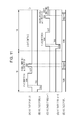
- FIG. 7 is a view representing an example of a voltage of DTL in FIG. 3 and FIG. 4 ;
- FIG. 8 is a wave form chart for illustrating an example of an action of a display device in FIG. 1 ;
- FIG. 9 is a wave form chart for illustrating an example of a scanning of the Vth correction and the signal writing and ⁇ correction in a display device in FIG. 1 ;
- FIG. 10 is a view representing an example of a wiring connection in a display panel in the related art.
- FIG. 11 is a wave form chart for illustrating an example of an action of a display device including a display panel in FIG. 10 ;
- FIG. 12 is a wave form chart for illustrating another example of an action of a display device including a display panel in FIG. 10 ;
- FIG. 13 is a view representing an example of a layout of each pixel in a display panel according to a comparative example
- FIG. 14 is a wave form chart for illustrating an example of an action of a display device including a display panel in FIG. 13 ;
- FIG. 15 is a view representing a modified example of a hard wiring configuration of a scanning line and a power line in FIG. 3 and FIG. 4 ;
- FIG. 16 is a view representing an example of a layout of each pixel in a display device according to the second embodiment of the present technology
- FIG. 17 is a view representing another modified example of a layout of each pixel in FIG. 16 ;
- FIG. 18 is an u′v′ chromaticity diagram in which the coordinates of RGBW and intermediate colors thereof are plotted;
- FIG. 19 is a wave form chart for illustrating an example of an action of a display device including a layout in FIG. 16 and FIG. 17 ;
- FIG. 20 is a view representing another modified example of a hard wiring configuration of a scanning line and a power line in FIG. 3 and FIG. 4 ;
- FIG. 21 is a view representing another modified example of a hard wiring configuration of a scanning line and a power line in FIG. 16 and FIG. 17 ;
- FIG. 22 is a perspective view representing the outside appearance in an Application Example 1 of a light emitting apparatus according to each embodiment described above;
- FIG. 23A is a perspective view representing the outside appearance viewed from the front in an Application Example 2 and FIG. 23B is a perspective view representing the outside appearance viewed from the other side;
- FIG. 24 is a perspective view representing the outside appearance in an Application Example 3;
- FIG. 25 is a perspective view representing the outside appearance in an Application Example 4.
- FIG. 26A is a front view of the state of being open in an Application Example 5
- FIG. 26B is a side view thereof
- FIG. 26C is a front view of the state of being closed
- FIG. 26D is a left-side view
- FIG. 26E is a right-side view
- FIG. 26F is a top view
- FIG. 26G is a bottom view.
- FIG. 1 represents a schematic configuration of a display device 1 according to the first embodiment of the present technology.
- This display device 1 includes a display panel 10 and a driving circuit 20 for driving the display panel 10 based on a picture signal 20 A and a synchronized signal 20 B which have been input externally.
- the driving circuit 20 for example, includes a timing generating circuit 21 , a picture signal processing circuit 22 , a signal line driving circuit 23 , a scanning line driving circuit 24 and a power line driving circuit 25 .
- the display panel 10 is a display panel in which a plurality of pixels 11 are arranged in two dimensions over the entire surface of a display region 10 A of the display panel 10 .
- the display panel 10 displays an image based on a picture signal 20 A which has been input externally by each pixel 11 being driven by an active-matrix driving by the driving circuit 20 .
- FIG. 2 represents an example of the configuration of a circuit of a pixel 11 .
- Each pixel 11 for example, includes a pixel circuit 12 and an organic EL element 13 .
- the organic EL element 13 for example, has a configuration in which an anode electrode, an organic layer and a cathode electrode are laminated in order.
- the organic EL element 13 includes an element capacity Coled (not shown).
- the pixel circuit 12 for example, is configured by a driving transistor Tr 1 , a writing transistor Tr 2 and a retention capacity Cs, and is a configuration of a circuit of 2Tr 1 C.
- the writing transistor Tr 2 controls an application of the signal voltage corresponding to the picture signal with respect to the gate of the driving transistor Tr 1 . Specifically, the writing transistor Tr 2 samples a voltage of a signal line DTL described later as well as writes into the gate of the driving transistor Tr 1 .
- the driving transistor Tr 1 drives the organic EL element 13 and is connected to the organic EL element 13 in series.
- the driving transistor Tr 1 controls the current which flows to the organic EL element 13 corresponding to the size of voltage which has been written by the writing transistor Tr 2 .
- the retention capacity Cs retains the predetermined voltage between a gate and a source of the driving transistor Tr 1 .
- the pixel circuit 12 may be configured by a circuit which is different from the configuration of a circuit of 2Tr1C described above.
- the pixel circuit 12 may be configured by a circuit of 2Tr 2 C in which an auxiliary capacity Csub is connected to the source of the driving transistor Tr 1 .
- the driving transistor Tr 1 and the writing transistor Tr 2 are formed by a thin film transistor (TFT) of an n-channel MOS type.
- TFT thin film transistor
- the kinds of TFTs are not particularly limited, for example, there may be a reverse stagger structure (a bottom gate type, as it is called) and there may be a stagger structure (a top gate type).
- the driving transistor Tr 1 and the writing transistor Tr 2 may be formed by a TFT of a p-channel MOS type.
- the display panel 10 includes a plurality of scanning lines WSL extending in the row direction, a plurality of signal lines DTL extending in the column direction and a plurality of power lines DSL extending in the row direction.
- the scanning line WSL is used for selecting each pixel 11 .
- the signal line DTL is used for supplying each pixel 11 with a signal voltage corresponding to a picture signal.
- the power line DSL is used for supplying each pixel 11 with the driving current.
- the pixels 11 are provided in the vicinity of the intersection between each signal line DTL and each scanning line WSL.
- Each signal line DTL is connected to an output terminal (not shown) of the signal line driving circuit 23 described later and the source or the drain of the writing transistor Tr 2 .
- Each scanning line WSL is connected to an output terminal (not shown) of the scanning line driving circuit 24 described later and the gate of the writing transistor Tr 2 .
- Each power line DSL is connected to an output terminal (not shown) of a power which outputs a fixed voltage and the source or the drain of the driving transistor Tr 1 .
- the gate of the writing transistor Tr 2 is connected to the scanning line WSL.
- the source or the drain of the writing transistor Tr 2 is connected to the signal line DTL and the terminal, which is not connected to the signal line DTL, out of the source and the drain of the writing transistor Tr 2 , is connected to the gate of the driving transistor Tr 1 .
- the source or the drain of the driving transistor Tr 1 is connected to the power line DSL and the terminal, which is not connected to the power line DSL, out of the source and the drain of the driving transistor Tr 1 , is connected to an anode of the organic EL element 13 .
- One end of the retention capacity Cs is connected to the gate of the driving transistor Tr 1 and another end of the retention capacity Cs is connected to the source of the driving transistor Tr 1 (the terminal of the organic EL element 13 side in FIG. 2 ). That is, the retention capacity Cs is inserted into between the gate and the source of the driving transistor Tr 1 .
- the display panel 10 further includes a ground line GND which is connected to a cathode of the organic EL element 13 as shown in FIG. 2 .
- the ground line GND is electrically connected to an external circuit (not shown) which is a ground potential.
- the ground line GND for example, is a sheet-like electrode which is formed over the entire display region 10 A.
- the ground line GND may be a belt-like electrode which is formed with a striped pattern corresponding to a pixel row or a pixel column.
- the display panel 10 further includes, for example, a frame region which does not display a picture on the periphery of the display region 10 A.
- the flame region for example, is covered by a light-resistant member.
- FIG. 3 and FIG. 4 represent an example of the configuration of a circuit in two display pixels 14 (described later) which are adjacent to each other in the column direction.
- FIG. 3 represents an example of a layout of each pixel 11 in the display pixel rows of n-th row (1 ⁇ n ⁇ N, N is the total number of the display pixel rows (even number)) and n+1-th row
- FIG. 4 represents an example of a layout of each pixel 11 in the display pixel rows of n+2-th row and n+3-th row.
- a display pixel row indicates a line which is formed by a plurality of display pixels 14 arranged alongside in the row direction.
- a pixel row indicates a line which is formed by a plurality of pixels 11 arranged alongside in the row direction and is equivalent to a subpixel row.
- the display pixel row and the pixel row substantially indicate the same lines and it is not necessary to use the display pixel row and the pixel row properly with each other.
- each pixel 11 in the display pixel rows of n-th row and n+1-th row and in the display pixel rows of n+2-th row and n+3-th row are common. So, hereinafter, in order to avoid a repeating description, description of the layouts of each pixel 11 in the display pixel rows of n+2-th row and n+3-th row will be omitted.
- Each pixel 11 corresponds to a dot of the minimum unit configuring a screen on the display panel 10 .
- the display panel 10 is a color display panel and the pixel 11 , for example, is equivalent to the subpixel which emits a single color light such as red, green or blue.
- a display pixel 14 is configured by three pixels 11 in which the kinds of luminescent colors are different from each other. That is, the number of the kinds of luminescent colors is three and the number of the pixels 11 which are included in each display pixel 14 is also three.
- Three pixels 11 included in the display pixel 14 are configured by a pixel 11 R which emits red light, a pixel 11 G which emits green light and a pixel 11 B which emits blue light.
- a plurality of scanning lines WSL are assigned with k's for one unit.
- the number of the display pixel rows included in one unit is two or more and the number of the kinds of luminescent colors or less. Therefore, k is satisfied with 2 ⁇ k ⁇ (the total number of the kinds of luminescent colors of the pixel 11 in one display pixel 14 ).
- a plurality of scanning lines WSL are assigned with two lines for one unit. Therefore, the number of the display pixel rows included in one unit is two and the number of the scanning lines WSL included in one unit is also two.
- the total number of the scanning lines WSL is equal to the total number of the display pixel rows and is N.
- n in FIG. 3 is a positive integer of one or more and N/2 or less and WSL (n) in FIG. 3 indicates the scanning line WSL of n-th number.
- Each scanning line WSL is connected to a plurality of pixels 11 of the same luminescent color within one unit. Specifically, in two of the scanning lines WSL (n) and WSL (n+1) included in one unit, the scanning line WSL (n) (the first scanning line) is connected to a plurality of pixels 11 G and a plurality of pixels 11 B included in one unit and the scanning line WSL (n+1) is connected to a plurality of pixels 11 R included in one unit.
- the scanning line WSL (n) is equivalent to a scanning line of “the upper row” or “the highest row” and the scanning line WSL (n+1) is equivalent to a scanning line of “the lower row” or “the bottom row”.
- the upper row indicates a scanning line which is selected in the first half in sequence of the signal writing within one unit.
- the highest row indicates a scanning line which is selected first in sequence of the signal writing within one unit.
- the lower row indicates a scanning line which is selected in the last half in sequence of the signal writing within one unit.
- the bottom row indicates a scanning line which is selected at the last in sequence of the signal writing within one unit.
- each scanning line WSL is connected to all pixels 11 of the same luminescent color within one unit.
- the scanning line WSL (n) is connected to all pixels 11 G and all pixels 11 B within one unit and the scanning line WSL (n+1) is connected to all pixels 11 R within one unit.
- a plurality of power lines DSL are assigned with one line for one unit. Therefore, the number of the power lines DSL included in one unit is one.
- j in FIG. 3 is a positive integer of one or more and N/2 or less and DSL (j) in FIG. 3 indicates a power line DSL of j-th number.
- Each power line DSL is connected to all pixels 11 within one unit. Specifically, one power line DSL included in one unit is connected to all pixels 11 ( 11 R, 11 G and 11 B) included in one unit.
- a plurality of signal lines DTL are assigned with a's (2 ⁇ a ⁇ (the total number of the subpixels in one pixel)) for each display pixel 14 in each display pixel row. Specifically, a plurality of the signal lines DTL are assigned with two lines for each display pixel 14 in each display pixel row. In a's of the signal lines DTL assigned for each display pixel 14 in each display pixel row, one signal line DTL (the first signal line) is connected to the pixels 11 of two kinds of luminescent colors which are not shared with the scanning line WSL in one display pixel 14 .
- one signal line DTL (the first signal line) is connected to the pixels 11 of two kinds of luminescent colors which do not share the scanning line WSL in one display pixel 14 and the other signal line DTL is connected to the pixels 11 of the remaining kinds (one kind or a plurality of kinds) of luminescent colors in one display pixel 14 .
- two display pixels 14 which are adjacent to each other in the column direction that is, two display pixels 14 in which rows are different from each other and are adjacent to each other within one unit
- two of the signal lines DTL (m) and DTL (m+2) are assigned.
- the number of the signal lines DTL is equal to the number of the pixels 11 included in one pixel row and is M (M is a multiple of 4).
- m is a positive integer of one or more and M ⁇ 4 or less, and is the number which is equivalent to (a multiple of 4+1) in a case of being other than 1. Therefore, DTL (m) in FIG. 3 indicates a signal line DTL of m-th number.
- one signal line DTL (m+2) (the first signal line) is connected to the pixels 11 R and 11 B of two kinds of luminescent colors which are not shared with the scanning line WSL in one display pixel 14 and the other signal line DTL (m) is connected to the pixel 11 G of the remaining one kind of luminescent color.
- the other signal line DTL (m) is connected to the pixel 11 G of the remaining one kind of luminescent color.
- two of the signal lines DTL (m+1) and DTL (m+3) are assigned.
- one signal line DTL (m+1) (the first signal line) is connected to the pixels 11 R and 11 B of two kinds of luminescent colors which are not shared with the scanning line WSL in one display pixel 14 and the other signal line DTL (m+3) is connected to the pixel 11 G of the remaining kinds of luminescent colors.
- two of signal lines DTL (m) and DTL (m+2) of an even number of column are assigned with respect to one display pixel 14 and two of signal lines DTL (m+1) and DTL (m+3) of an odd number of column are assigned with respect to the other display pixel 14 .
- the total number of the signal lines DTL is suppressed to a minimum.
- the combination of the luminescent colors of the pixels 11 of two kinds of luminescent colors which share the scanning line WSL is equal to each other.
- the arrangements of the luminescent colors are different from each other. For example, in the upper row within one unit, three pixels 11 are arranged in the row direction in the order of GRB and in the lower row within one unit, three pixels 11 are arranged in the row direction in the order of BRG.
- FIG. 5 is a xy chromaticity diagram in which the coordinates of the chromaticity of the luminescent color of three pixels 11 included in the display pixel 14 are plotted.
- FIG. 6 is an u′v′ chromaticity diagram in which the coordinates (the single color coordinates) of the chromaticity of the luminescent color of three pixels 11 included in the display pixel 14 are plotted again using the formulae 1, 2 and 3 as follows.
- A, B and C in FIG. 6 are plots of the coordinates (the mixed color coordinates) in an u′v′ chromaticity diagram of three mixed colors capable of being formed by using two arbitrary colors out of three luminescent colors included in one display pixel 14 .
- a in FIG. 6 is a plot of the coordinates in an u′v′ chromaticity diagram of the mixed colors of the luminescent color (red) of pixel 11 R and the luminescent color (green) of the pixel 11 G.
- B in FIG. 6 is a plot of the coordinates in an u′v′ chromaticity diagram of the mixed colors of the luminescent color (green) of the pixel 11 G and the luminescent color (blue) of the pixel 11 B.
- C in FIG. 6 is a plot of the coordinates in an u′v′ chromaticity diagram of the mixed colors of the luminescent color (blue) of the pixel 11 B and the luminescent color (red) of the pixel 11 R.
- each scanning line WSL is connected to a plurality of pixels 11 of the same luminescent color within one unit.
- the scanning line WSL (the first scanning line) of the highest row is connected to the pixels 11 of one kind or a plurality of kinds of luminescent colors including the pixel 11 of the luminescent color in which the distance between the single color coordinates and the mixed color coordinates is relatively the shortest.
- the pixel 11 of the luminescent color in which the distance between the single color coordinates and the mixed color coordinates is relatively the shortest is the pixel 11 G according to FIG. 6 .
- the scanning line WSL (the first scanning line) of the highest row is connected to the pixels 11 G and 11 B of two kinds of luminescent colors including the pixel 11 G in which the distance between the single color coordinates and the mixed color coordinates is relatively the shortest.
- the scanning line WSL of the bottom row is connected to the pixel 11 R of one kind of luminescent color.
- the scanning line WSL (the first scanning line) of the highest row may be connected to the pixels 11 G and 11 R of two kinds of luminescent colors including the pixel 11 G in which the distance between the single color coordinates and the mixed color coordinates is relatively the shortest.
- the scanning line WSL of the bottom row is connected to the pixel 11 B of one kind of the luminescent color.
- one signal line DTL (the first signal line) is connected to the pixels 11 of two kinds of luminescent colors which are not shared with the scanning line WSL in one display pixel 14 .
- two signal lines DTL are assigned for each display pixel 14 in each display pixel row and further, the number of the kinds of luminescent colors included in one display pixel 14 is three.
- one signal line DTL (the first signal line) is connected to the pixels 11 of the two kinds of luminescent colors other than the pixel 11 of the luminescent color in which the distance between the single color coordinates and the mixed color coordinates is relatively the shortest.
- the pixel 11 of the luminescent color in which the distance between the single color coordinates and the mixed color coordinates is relatively the shortest is the pixel 11 G according to FIG. 6 . Therefore, for example, one signal line DTL (the first signal line) is connected to the pixels 11 R and 11 B of two kinds of luminescent colors other that the pixel 11 G. At this time, the remaining signal line DTL is connected to the pixel 11 G.
- the driving circuit 20 for example, includes a timing generating circuit 21 , a picture signal processing circuit 22 , a signal line driving circuit 23 , a scanning line driving circuit 24 and a power line driving circuit 25 as described above.
- the timing generating circuit 21 is a control circuit so that each circuit operates together within the driving circuit 20 .
- the timing generating circuit 21 for example, outputs a control signal 21 A with respect to each circuit described above according to a synchronized signal 20 B which have been input externally (synchronizing).
- the picture signal processing circuit 22 performs the predetermined correction with respect to a digital picture signal 20 A which has been input externally and outputs a picture signal 22 A which has been obtained thereby into the signal line driving circuit 23 .
- the predetermined correction for example, a ⁇ correction, an overdrive correction, and the like are included.
- the signal line driving circuit 23 applies an analog signal voltage of corresponding to the picture signal 22 A which has been input from the picture signal processing circuit 22 according to an input of a control signal 21 A (synchronizing) to each signal line DTL.
- the signal line driving circuit 23 for example, is able to output two kinds of voltages (Vofs and Vsig). Specifically, the signal line driving circuit 23 supplies the pixel 11 which has been selected by the scanning line driving circuit 24 with two kinds of voltages (Vofs and Vsig) through the signal line DTL.
- FIG. 7 represents an example of the voltage V (n), V (n+1), V (n+2) and V (n+3) applied in order according to scanning of the scanning line WSL with respect to four signal lines DTL (DTL (m), DTL (m+1), DTL (m+2) and DTL (m+3)) which have been connected to four display pixels 14 arranged in the column direction in two units which are adjacent to each other in the column direction.
- the signal line driving circuit 23 outputs a signal voltage V (n) corresponding to the selection of the scanning line WSL (n) and outputs a signal voltage V (n+1) corresponding to the selection of the scanning line WSL (n+1).
- the signal line driving circuit 23 outputs a signal voltage V (n+2) corresponding to the selection of the scanning line WSL (n+2) and outputs a signal voltage V (n+3) corresponding to the selection of the scanning line WSL (n+3).
- the scanning line driving circuit 24 selects the scanning lines WSL in the order of WSL (n), WSL (n+1), WSL (n+2) and WSL (n+3) on the occasion of the writing of the signal voltage as described later. Therefore, the signal line driving circuit 23 outputs the signal voltages Vsigs in the order of V (n), V (n+1), V (n+2) and V (n+3) on the occasion of the writing of the signal voltage.
- the signal line driving circuit 23 supplies the voltages Vsigs (Vsig (n, m) and Vsig (n, m+2)) corresponding to the n display pixel row with respect to a plurality of pixels 11 which belong to the n display pixel row out of a plurality of pixels 11 which has been selected at the same time by the scanning line driving circuit 24 through even-numbers of the signal lines DTL (m) and DTL (m+2), as shown in FIG. 7 .
- the signal line driving circuit 23 supplies the voltages Vsigs (Vsig (n+1, m+1) and Vsig (n+1, m+3)) corresponding to the n+1 display pixel row with respect to a plurality of pixels 11 which belong to the n+1 pixel rows out of a plurality of pixels 11 selected at the same time by the scanning line driving circuit 24 through odd-numbers of the signal lines DTL (m+1) and DTL (m+3).
- the signal line driving circuit 23 outputs the voltages Vsig (n, m) and Vsig (n, m+2) corresponding to the n display pixel row with respect to even-numbers of the signal lines DTL (m) and DTL (m+2) and outputs the voltages Vsig (n, m+1) and Vsig (n, m+3) corresponding to the n+1 display pixel row with respect to odd-numbers of the signal lines DTL (m+1) and DTL (m+3) at the same time.
- the signal line driving circuit 23 when the scanning line WSL (n+1) has been selected on the occasion of the signal writing, the signal line driving circuit 23 outputs the voltages Vsig (n+1, m) and Vsig (n+1, m+2) corresponding to the n+1 display pixel row with respect to even-numbers of the signal lines DTL (m) and DTL (m+2) and outputs the voltages Vsig (n, m+1) and Vsig (n, m+3) corresponding to the n display pixel row with respect to odd-numbers of the signal lines DTL (m+1) and DTL (m+3) at the same time.
- the signal line driving circuit 23 also applies the voltage corresponding to the n+2 pixel row and the n+3 pixel row in the same way as the n pixel row and n+1 pixel row.
- Vsig is the voltage value corresponding to the picture signal 20 A.
- Vofs is the constant voltage which is not related to the picture signal 20 A.
- the minimum voltage of Vsig is the voltage value lower than Vofs and the maximum voltage of Vsig is the voltage value higher than Vofs.
- the scanning line driving circuit 24 performs the Vth correction, the writing of the signal voltage Vsig and the ⁇ correction in the desired order by selecting a plurality of scanning lines WSL using the predetermined sequence according to the input of the control signal 21 A (synchronizing).
- the Vth correction indicates the correction action in which the voltage Vgs between the gate and the source of the driving transistor Tr 1 is set close to the threshold voltage of the driving transistor.
- the writing of the signal voltage Vsig indicates the action which writes the signal voltage Vsig with respect to the gate of the driving transistor Tr 1 through the writing transistor Tr 2 .
- the ⁇ correction indicates the action which corrects the voltage Vgs retained between the gate and the source of the driving transistor Tr 1 according to the size of the mobility ⁇ of the driving transistor Tr 1 .
- the signal writing and ⁇ correction are often performed at the different timing to each other. In the embodiment, by one selective pulse being input into the scanning line WSL, the scanning line driving circuit 24 performs the signal writing and the ⁇ correction at the same time (or continuously without interval).
- the driving circuit 20 collectively performs the Vth correction and the signal writing for each unit. Specifically, after performing the Vth correction and the signal writing in the first unit, the driving circuit 20 performs the Vth correction and the signal writing in the second unit which is adjacent to the first unit in the column direction, as shown in FIG. 9 . That is, the driving circuit 20 performs a series of actions (the Vth correction and the signal writing) per unit in order.
- the scanning line driving circuit 24 selects all scanning lines WSL included in one unit at the same time (or at the same period) as the Vth correction. Specifically, the scanning line driving circuit 24 selects two of the scanning lines WSL (n) and WSL (n+1) included in one unit at the same time (or at the same period) as the Vth correction. That is, the scanning line driving circuit 24 selects a plurality of pixels 11 (for example, pixels 11 R, 11 G and 11 B) in the n display pixel row and a plurality of pixels 11 (for example, pixels 11 R, 11 G and 11 B) in the n+1 display pixel row at the same time (or at the same period) as the Vth correction.
- a plurality of pixels 11 for example, pixels 11 R, 11 G and 11 B
- a plurality of pixels 11 for example, pixels 11 R, 11 G and 11 B
- the scanning line driving circuit 24 selects a plurality of the scanning lines WSL included in one unit in order in the same direction as the scanning direction (hereinafter, referred to as a “unit scanning direction”) of performing a series of actions (the Vth correction and the signal writing) per unit in order on the occasion of the signal writing.
- the unit scanning direction for example, is the direction parallel to the direction from the upper end side toward the lower end side of the display panel 10 . Therefore, after performing the signal writing into each pixel 11 in one display pixel row with respect to each pixel 11 connected to the scanning line WSL (n), the scanning line driving circuit 24 performs the signal writing with respect to each pixel 11 connected to the scanning line WSL (n+1).
- the unit scanning direction may be the direction parallel to the direction from the upper end side toward the lower end side of the display panel 10 .
- the scanning line driving circuit 24 after performing the signal writing into each pixel 11 in one display pixel row with respect to each pixel 11 connected to the scanning line WSL (n+1), the scanning line driving circuit 24 performs the signal writing with respect to each pixel 11 connected to the scanning line WSL (n).
- the scanning line driving circuit 24 selects two of scanning lines WSL (n) and WSL (n+1) included in one unit in the order of the scanning line WSL (n) and the scanning line WSL (n+1) on the occasion of the signal writing. Therefore, after selecting two kinds of pixels 11 G and 11 B in the n display pixel row and two kinds of pixels 11 G and 11 B in the n+1 display pixel row through the scanning line WSL (n) at the same time, the scanning line driving circuit 24 selects one kind of pixel 11 R in the n display pixel row and one kind of pixel 11 R in the n+1 display pixel row through the scanning line WSL (n+1) at the same time, as the signal writing.
- the scanning line driving circuit 24 is able to output two kinds of voltages (Von and Voff). Specifically, the scanning line driving circuit 24 supplies the pixel 11 targeted for driving with two kinds of voltages (Von and Voff) through the scanning line WSL and performs an on-off control of the writing transistor Tr 2 .
- Von is the value which is greater than or equal to the on-state voltage of the writing transistor Tr 2 .
- Von is the peak value of a writing pulse which is output in “the latter half portion of the Vth correction preparation period”, “Vth correction period”, “Signal writing and ⁇ correction period” or the like described later from the scanning line driving circuit 24 .
- Voff is the value which is lower than on-state voltage of the writing transistor Tr 2 and is lower than Von.
- Voff is the peak value of a writing pulse which is output into “the first half portion of the Vth correction preparation period”, “light emitting period” or the like described later from the scanning line driving circuit 24 .
- the power line driving circuit 25 selects a plurality of power lines DSL for each predetermined unit in order according to the input of the control signal 21 A (synchronizing).
- the power line driving circuit 25 for example, is able to output two kinds of voltages (Vcc and Vss).
- the power line driving circuit 25 supplies the entire one unit (that is, all pixels 11 included in one unit) including pixel 11 selected by the scanning line driving circuit 24 with two kinds of voltages (Vcc and Vss) through the power line DSL.
- Vss is the voltage value which is lower than the voltage (Ve 1 +Vcath) in which the threshold voltage Ve 1 of the organic EL element 13 and the cathode voltage Vcath of the organic EL element 13 are added together.
- Vcc is the voltage value which is greater than or equal to the voltage (Ve 1 +Vcath).
- the actions (the actions from extinction to light emitting) of the display device 1 in the embodiment will be described.
- the embodiment even though I-V characteristics of the organic EL element 13 are changed according to time course and the threshold voltage and the mobility of the driving transistor Tr 1 are changed according to time course, without being affected thereby the compensation action with respect to the change of I-V characteristics of the organic EL element 13 and the correction action with respect to the change of the threshold voltage and the mobility of the driving transistor Tr 1 are incorporated in order to maintain a uniform light emitting luminance of the organic EL element 13 .
- FIG. 8 represents an example of various kinds of wave forms in the display device 1 .
- FIG. 8 shows the state in which the change in two values of the voltages occurs every moment in the scanning line WSL, the power line DSL and the signal line DTL.
- FIG. 8 shows the state in which the gate voltage Vg and the source voltage Vsof of the driving transistor Tr 1 change every moment according to the change in the voltage of the scanning line WSL, the power line DSL and the signal line DTL.
- the driving circuit 20 performs the preparation of the Vth correction in which the voltage Vgs between the gate and the source of the driving transistor Tr 1 is set close to the threshold voltage of the driving transistor Tr 1 .
- the voltage of the scanning line WSL is set as Voff
- the voltage of the signal line DTL is set as Vofs
- the voltage of the power line DSL is set as Vcc (that is, when the organic EL element 13 is emitted)
- the power line driving circuit 25 decreases the voltage of the power line DSL from Vcc to Vss according to the control signal 21 A (T 1 ).
- the source voltage Vs is decreased to Vss and the organic EL element 13 is quenched.
- the gate voltage Vg is also decreased by a coupling through the retention capacity Cs.
- the scanning line driving circuit 24 increases the voltage of the scanning line WSL from Voff to Von according to the control signal 21 A (T 2 ). Then, the gate voltage Vg is decreased to Vofs. At this time, the potential difference Vgs between the gate voltage Vg and the source voltage Vs may be smaller than, equal to or bigger than the threshold voltage of the driving transistor Tr 2 .
- the driving circuit 20 performs the Vth correction. Specifically, while the voltage of the signal line DTL is set as Vofs and the voltage of the scanning line WSL is set as Von, the power line driving circuit 25 increases the voltage of the power line DSL from Vss to Vcc according to the control signal 21 A (T 3 ). Then, current Ids flows into between the drain and the source of the driving transistor Tr 1 and the source voltage Vs rises. At this time, in a case where the source voltage Vs is lower than Vofs-Vth (in a case where the Vth correction has not been completed yet), the current Ids flows into between the drain and the source of the driving transistor Tr 1 until the driving transistor Tr 1 is cut-off (until the potential difference Vgs becomes Vth). In so doing, the gate voltage Vg becomes Vofs, the source voltage Vs rises, and as a result, the retention capacity Cs is charged Vth and the potential difference Vgs becomes Vth.
- the scanning line driving circuit 24 decreases the voltage of the scanning line WSL from Von to Voff according to the control signal 21 A (T 4 ). Then, since the gate of the driving transistor Tr 1 becomes floating, it is possible to maintain the potential difference Vgs as Vth in spite of the size of the voltage of the signal line DTL. In doing so, by setting the potential difference Vgs as Vth, even in a case where the threshold voltages Vth of the driving transistor Tr 1 vary for each pixel circuit 12 , it is possible to stop the variability of the light emitting luminance of the organic EL element 13 .
- the signal line driving circuit 23 switches the voltage of the signal line DTL from Vofs to Vsig.
- the driving circuit 20 After finishing the Vth correction dormant period (that is, after completing the Vth correction period), the driving circuit 20 performs the writing of the signal voltage and the ⁇ correction according to the picture signal 20 A. Specifically, while the voltage of the signal line DTL is set as Vsig and the voltage of the power line DSL is set as Vcc, the scanning line driving circuit 24 increases the voltage of the scanning line WSL from Voff to Von according to the control signal 21 A (T 5 ) and makes the gate of the driving transistor Tr 1 connect to the signal line DTL. Then, the gate voltage Vg of the driving transistor Tr 1 becomes the voltage Vsig of the signal line DTL.
- the anode voltage of the organic EL element 13 is still smaller than the threshold voltage Ve 1 of the organic EL element 13 at this stage and the organic EL element 13 is cut-off. Therefore, since the current Ids flows into the element capacity Coled of the organic EL element 13 and the element capacity Coled is charged, the source voltage Vs rises by only ⁇ Vs and eventually, the potential difference Vgs becomes Vsig+Vth ⁇ Vs. In this way, the writing and the ⁇ correction are performed at the same time.
- the bigger the mobility ⁇ of the driving transistor Tr 1 is, the bigger ⁇ Vs is and therefore, it is possible to remove the variability of the mobility ⁇ for each pixel 11 by making the potential difference Vgs smaller by only ⁇ V before the emission of light.
- the scanning line driving circuit 24 decreases the voltage of the scanning line WSL from Von to Voff according to the control signal 21 A (T 6 ). Then, the gate of the driving transistor Tr 1 becomes floating, the current Ids flows into between the drain and the source of the driving transistor Tr 1 and the source voltage Vs rises. As a result, the voltage which is greater than or equal to the threshold voltage Ve 1 is applied to the organic EL element 13 and the organic EL element 13 emits light with the desired luminance.
- FIG. 9 represents an example of the scanning of the Vth correction and the signal writing and ⁇ correction in two units which are adjacent to each other in the column direction.
- all pixels 11 G and all pixels 11 B within one unit are set as one group and all pixels 11 R within one unit are set as one group. So, below, all pixels 11 G and all pixels 11 B within a unit in which the scanning lines WSL (n) and WSL (n+1) have been connected, are set as the first group and all pixels 11 R within the unit are set as the second group. In addition, all pixels 11 G and all pixels 11 B within a unit in which the scanning lines WSL (n+2) and WSL (n+3) have been connected, are set as the third group and all pixels 11 R within the unit are set as the fourth group.
- the driving circuit 20 After performing the Vth correction with respect to all groups (the first and the second group) within one unit at the same period, the driving circuit 20 performs the writing of the signal voltage for each group with respect to all groups (the first and the second group) within the unit in order. At this time, after performing the signal writing with respect to the first group of the pixels 11 connected to the scanning line WSL (n) of the highest row, the driving circuit 20 performs the signal writing with respect to the second group of the pixels 11 connected to the scanning line WSL (n+1) of the bottom row.
- the driving circuit 20 After this, after performing the Vth correction with respect to all groups (the third and the fourth group) within the next unit at the same period, the driving circuit 20 performs the writing of the signal voltage for each group with respect to all groups (the third and the fourth group) within the unit in order. At this time, after performing the signal writing with respect to the first group of the pixels 11 connected to the scanning line WSL (n+2) of the highest row, the driving circuit 20 performs the signal writing with respect to the second group of the pixels 11 connected to the scanning line WSL (n+3) of the bottom row in the same way as described above.
- the driving circuit 20 performs the signal writing within the next horizontal period (1H). That is, the driving circuit 20 continuously uses two horizontal periods (2H) with respect to one unit to perform the Vth correction and the signal writing.
- the driving circuit 20 when performing the signal writing for each group, performs the signal writing at the same time with respect to all pixels 11 included in the group. Specifically, when the scanning line WSL (n) has been selected, the driving circuit 20 output the voltage V (n) described above with respect to each signal line DTL.
- the driving circuit 20 outputs Vsig (Vsig (n, m) and Vsig (n, m+2)) of the n-pixel row with respect to even-numbers of the signal lines DTL (DTL (m) and DTL (m+2)) and outputs the voltage Vsig (Vsig (n+1, m+1) and Vsig (n+1, m+3)) corresponding to the n+1-pixel row with respect to odd-numbers of the signal lines DTL (m+1) and DTL (m+3) at the same time.
- the driving circuit 20 outputs Vsig (Vsig (n+1, m) and Vsig (n+1, m+2)) of the n+1-pixel row with respect to even-numbers of the signal lines DTL (DTL (m) and DTL (m+2)) and outputs the voltage Vsig (Vsig (n, m+1) and Vsig (n, m+3)) corresponding to the n-pixel row with respect to odd-numbers of the signal lines DTL (m+1) and DTL (m+3) at the same time.
- the waiting times ⁇ t 1 in a plurality of pixels 11 G correspond for each pixel row.
- the waiting times ⁇ t 2 of each pixel 11 B are equal to the waiting times ⁇ t 1 of each pixel 11 G. Therefore, since the waiting times ⁇ t 2 also correspond in each pixel 11 B of the same luminescent color, the waiting times ⁇ t 2 in a plurality of pixels 11 B correspond for each pixel row.
- the waiting times ⁇ t 3 are also correspondent in each pixel 11 R of the same luminescent color, the waiting times ⁇ t 3 in a plurality of pixels 11 R correspond for each pixel row.
- the waiting times ⁇ t 1 and ⁇ t 2 of the pixels 11 G and 11 B and the waiting times ⁇ t 3 of the pixel 11 R are different from each other and however, this slightly affects only the color reproductivity and dose not affect the color shading.
- the driving circuit 20 After performing the writing of the signal voltage into each pixel 11 in one unit with respect to pixels 11 (for example, pixels 11 G and 11 B) of one kind or a plurality of kinds of luminescent colors including the pixels 11 (for example, pixel 11 G) of the luminescent color in which the distance between the single color coordinates and the mixed color coordinates is relatively the shortest, the driving circuit 20 performs the writing of the signal voltage with respect to pixels 11 (for example, pixel 11 R) of one kind or a plurality of kinds of luminescent colors in which the kinds of luminescent colors are different from these pixels 11 . In so doing, in sequence of the signal writing within one unit, it is possible to perform the signal writing into the pixels 11 of the luminescent color in which the distance between the single color coordinates and the mixed color coordinates is relatively the shortest first.
- FIG. 10 represents an example of an arrangement of a pixel which generally is used in the related art.
- each pixel of 11 R, 11 G and 11 B included in a display pixel 140 is connected to the common scanning line WSL (n) and the power line DSL (n).
- WSL (n) the common scanning line
- DSL (n) the power line DSL
- This driving method is suited for a high speed driving due to the Vth correction being bundled.
- the waiting times ⁇ t from the finish of the Vth correction to the start of the signal writing are different for each line. Therefore, even though the signal voltage of the same gradation is applied to the gate of the driving transistor of each line, the light emitting luminance becomes different for each line, and therefore, there was a problem in which the luminance unevenness occurred.
- each scanning line WSL used for selecting each pixel 11 is connected to a plurality of pixels 11 of the same luminescent color within one unit.
- each power line DSL used for supplying each pixel 11 with the driving current is connected to all pixels 11 within one unit.
- FIG. 13 represents an example of an arrangement of a pixel according to a comparative example.
- the scanning line (n) of the highest row out of two of the scanning lines WSL (n) and (n+1) assigned for one unit is connected to the pixels 11 (here, pixels 11 R and 11 B) of the two kinds of luminescent colors other than the pixel 11 (here, pixel 11 G) of the luminescent color in which the distance between the single color coordinates and the mixed color coordinates is relatively the shortest. Therefore, in sequence of the signal writing within one unit, the signal writing into the pixels 11 R and 11 B is followed by performance of the signal writing into the pixel 11 G as shown FIG. 14 .
- the scanning line (the scanning line WSL (n)) of the highest row out of k's of the scanning lines WSL assigned for one unit is connected to the pixels 11 (hereinafter, referred as a “specific pixel 11 ”) (for example, pixels 11 G and 11 B) of one kind or a plurality of kinds of luminescent colors including the pixel 11 (here, pixel 11 G) of the luminescent color in which the distance between the single color coordinates and the mixed color coordinates is relatively the shortest.
- the signal writing into the specific pixel 11 is performed first.
- timing margin is not limited by the signal writing of the latter part when the signal writing into the specific pixel 11 is performed, even though the 1H period is considerably shorten, it is possible to take the adequate timing margin. Therefore, it is possible to decrease the occurrence of the luminance unevenness and the chromaticity shift due to transient when driving with high speed.
- each scanning line WSL (WSL (n) to WSL(n+3)) includes the same number of the branch (that is, two branches) as the number of the pixel rows included in one unit.
- each branch is connected to each other within the display panel 10 .
- a connecting point C 1 among the branches may be within the display region 10 A or may be within the periphery of the display region 10 A (the flame region).
- each scanning line WSL is intersected with the other scanning lines WSL within the same unit.
- each power line DSL (DSL (j) and DSL (j+1)) also includes the same number of the branch (that is, two branches) as the number of the pixel rows included in one unit.
- each branch is also connected to each other within the display panel 10 .
- a connecting point C 2 among the branches may be within the display region 10 A or may be within the periphery of the display region 10 A (the flame region). In this way, by being provided with the branches in each scanning line WSL and each power line DSL, it is possible to widen the spacing between each scanning line WSL or the spacing between each power line DSL. As a result, a wiring layout is facilitated.
- FIG. 16 represents an example of a layout of each display pixel 14 in the display device 1 according to the second embodiment of the present technology.
- the display pixel 14 is configured by four kinds or more of pixels 11 in which the luminescent colors are different from each other.
- the display pixel 14 is configured by four kinds of pixels 11 R, 11 G, 11 B and 11 W in which the luminescent colors are different from each other as shown in FIG. 16 and FIG. 17 .
- FIG. 16 and FIG. 17 represent an example of the configuration of a circuit in two display pixels 14 which are adjacent to each other in the column direction.
- FIG. 16 represents an example of the configuration of a circuit of each display pixel 14 in the display pixel rows of n-th row (1 ⁇ n ⁇ N, N is the total number of the display pixel rows (even numbers)) and n+1-th row.
- FIG. 17 represents an example of the configuration of a circuit of each display pixel 14 in the display pixel rows of n+2-th row and n+3-th row.
- a pixel 11 W is the pixel emitting white light and has the same configuration as the other pixels of 11 R, 11 G and 11 B.
- a pixel 11 Y emitting yellow light may be provided instead of the pixel 11 W.
- four pixels 11 are set as a so-called four-square arrangement and are arranged in a 2 ⁇ 2 matrix.
- four pixels 11 are set as the common color arrangement.
- the pixel 11 R is arranged at the upper left in the four-square arrangement
- the pixel 11 G is arranged at the lower left in the four-square arrangement
- the pixel 11 B is arranged at the lower right in the four-square arrangement
- the pixel 11 W is arranged at the upper right in the four-square arrangement as shown in FIG. 16 .
- one display pixel row is considered as the standard display pixel 14 .
- k's (k ⁇ 2) of the display pixel rows are set as one unit, a plurality of scanning lines WSL are assigned with k's for one unit.
- the number of the display pixel rows included in one unit is two or more and equal to or lower than the number of the kinds of luminescent colors.
- a plurality of the scanning lines WSL are assigned with two lines for one unit. Therefore, the number of the display pixel rows included in one unit is two and the number of the scanning lines WSL included in one unit is also two.
- the total number of the scanning lines WSL is equal to the total number of the display pixel rows and is N.
- n in FIG. 3 is a positive integer of one or more and N/2 or less and WSL (n) in FIG. 3 means the scanning line WSL of n-th number (n-th row).
- Each scanning line WSL is connected to a plurality of pixels 11 of the same luminescent color within one unit. Specifically, in two of the scanning lines WSL (n) and WSL (n+1) included in one unit, the scanning line WSL (n) is connected to a plurality of pixels 11 G and a plurality of pixels 11 W included in one unit and the scanning line WSL (n+1) is connected to a plurality of pixels 11 R and a plurality of pixels 11 B included in one unit. In addition, each scanning line WSL is connected to all pixels 11 of the same luminescent color within one unit.
- the scanning line WSL (n) is connected to all pixels 11 G and all pixels 11 W within one unit and the scanning line WSL (n+1) is connected to all pixels 11 R and all pixels 11 B within one unit.
- the combination of the luminescent colors of the pixels 11 of two kinds of luminescent colors which are shared with the scanning line WSL is equal to each other.
- Each scanning line WSL (WSL (n) to WSL(n+3)) includes the same number of the branches (that is, two branches (the first wiring and the second wiring)) as the number of the subpixel rows included in one display pixel row.
- Each of the first wirings is assigned with one wiring with respect to the subpixel row of the upper row in each display pixel row within one unit.
- Each of the first wirings is connected to a plurality of pixels 11 of the same luminescent color within one unit.
- Each of the second wirings is assigned with one wiring with respect to the subpixel row of the lower row the in each display pixel row within one unit.
- Each of the second wirings is connected to a plurality of pixels 11 of the luminescent color which is different form the luminescent color of the pixel 11 connected to the first wiring and the same luminescent color within one unit.
- each branch is connected to each other within the display panel 10 .
- a connecting point C 1 among the branches may be within the display region 10 A or may be within the periphery of the display region 10 A (the flame region).
- each scanning line WSL is intersected with the other scanning lines WSL within the same unit.
- the branches of each scanning line WSL cross the center of the four-square arrangement.
- the gate electrode 14 A of the writing transistor Tr 2 is connected to the branch of the scanning line WSL.
- a plurality of power lines DSL are assigned with one line for one unit. Therefore, the number of the power lines DSL included in one unit is one.
- j in FIG. 16 is a positive integer of one or more and N/2 or less and DSL (j) in FIG. 16 means the power line DSL of j-th number.
- Each power line DSL is connected to all pixels 11 within one unit. Specifically, one power line DSL included in one unit is connected to all pixels 11 ( 11 R, 11 G, 11 B and 11 W) included in one unit.
- each power line DSL (DSL (j) and DSL (j+1)) includes the same number of branches (that is, two branches) as the number of the display pixel rows included in one unit.
- each branch is also connected to each other within the display panel 10 .
- a connecting point C 2 among the branches may be within the display region 10 A or may be within the periphery of the display region 10 A (the flame region).
- the branches of each power line DSL cross the center of the four-square arrangement.
- a plurality of signal lines DTL are assigned with two lines for the display pixel 14 in each display pixel row.
- one signal line DTL is connected to the pixels 11 of two kinds of luminescent colors which are not shared with the scanning line WSL and the other signal line DTL is connected to the pixels 11 of two remaining kinds of luminescent colors.
- two display pixels 14 described above are equivalent to two display pixels 14 in which the display pixel rows are different from each other and are adjacent to each other in the column direction within one unit.
- two of the signal lines DTL (m) and DTL (m+2) are assigned.
- two of the signal lines DTL (m+2) and DTL (m+3) are assigned.
- two of the signal lines DTL (m) and DTL (m+2) of an even number of row are assigned with respect to one display pixel 14 and two of the signal lines DTL (m+1) and DTL (m+3) of an odd number of rows are assigned with respect to the other display pixel 14 .
- the total number of the signal lines DTL is suppressed to a minimum.
- a plurality of signal lines DTL are assigned with four lines for two display pixels 14 which are adjacent to each other in the column direction. Therefore, the total number of the signal lines DTL is M (M is a multiple of 4).
- M is a multiple of 4
- m is a positive integer of one or more and equal to or lower than M ⁇ 4 and is the number which is equivalent to (a multiple of 4+1) in a case of being other than 1. Therefore, DTL (m) in FIG. 16 means the signal line DTL of m-th number.
- DTL (m) in FIG. 16 means the signal line DTL of m-th number.
- DTL (m) In two display pixels 14 which are adjacent to each other in the column direction, for example, four of the signal lines DTL (m), DTL (m+1), DTL (m+2) and DTL (m+3) are assigned.
- each display pixel 14 Four of the signal lines DTL (m), DTL (m+1), DTL (m+2) and DTL (m+3) are arranged in line in this order in the row direction.
- two pixels 11 at the left side out of four pixels 11 are sandwiched between the signal line DTL (m) and the signal line DTL (m+1) from the row direction.
- two pixels 11 at the right side out of four pixels 11 are sandwiched between the signal line DTL (m+2) and the signal line DTL (m+3) from the row direction.
- two pixels 11 in which the luminescent colors are equal to each other are arranged between the common two signal lines DTL.
- two pixels 11 R are arranged between two of the signal lines DTL (m) and DTL (m+1).
- two pixels 11 G are arranged between two of the signal lines DTL (m) and DTL (m+1).
- two pixels 11 B are arranged between two of the signal lines DTL (m+2) and DTL (m+3).
- two pixels 11 W are arranged between two of the signal lines DTL (m+2) and DTL (m+3).
- Two of the signal lines DTL (m) and DTL (m+2) described above are respectively connected to the pixels 11 of two kinds of luminescent colors in which the scanning lines WSL are not shared to each other.
- the signal line DTL (m) is connected to the pixels 11 R and 11 G of two kinds of luminescent colors in which the scanning lines WSL are not shared to each other and the signal line DTL (m+2) is connected to the pixels 11 B and 11 W of two kinds of luminescent colors in which the scanning lines WSL are not shared to each other.
- the display pixel 14 included in the pixel row of n+1-th row out of two display pixels 14 described above is assigned with two of the signal lines DTL (m+1) and DTL (m+3).
- Two of the signal lines DTL (m+1) and DTL (m+3) are respectively connected to the pixels 11 of two kinds of luminescent colors in which the scanning lines WSL are not shared to each other.
- the signal line DTL (m+1) is connected to the pixels 11 R and 11 G of two kinds of luminescent colors in which the scanning lines WSL are not shared to each other and the signal line DTL (m+3) is connected to the pixels 11 B and 11 W of two remaining kinds of luminescent colors.
- the combination of the luminescent colors of the pixels 11 of two kinds of luminescent colors, which are shared with the scanning line WSL, is equal to each other.
- the arrangement of the luminescent color is also equal to each other.
- FIG. 18 is an u′v′ chromaticity diagram in which the coordinates (the single color coordinates) of the chromaticity of the luminescent color of four pixels 11 included in the display pixel 14 are plotted again using the formulae 1, 2 and 3 described above.
- a to D in FIG. 18 are plots of the coordinates (the mixed color coordinates) in an u′v′ chromaticity diagram of four mixed colors capable of being formed by using two arbitrary colors out of four luminescent colors included in one display pixel 14 .
- a in FIG. 18 is a plot of the coordinates in an u′v′ chromaticity diagram of the mixed colors of the luminescent color (red) of the pixel 11 R and the luminescent color (green) of the pixel 11 G.
- B in FIG. 18 is a plot of the coordinates in an u′v′ chromaticity diagram of the mixed colors of the luminescent color (green) of the pixel 11 G and the luminescent color (blue) of the pixel 11 B.
- C in FIG. 18 is a plot of the coordinates in an u′v′ chromaticity diagram of the mixed colors of the luminescent color (blue) of the pixel 11 B and the luminescent color (red) of the pixel 11 R.
- D in FIG. 18 is a plot of the coordinates in an u′v′ chromaticity diagram of the mixed colors of the luminescent color (red) of the pixel 11 R and the luminescent color (white) of the pixel 11 W.
- FIG. 18 is a plot of the coordinates in an u′v′ chromaticity diagram of the mixed colors of the luminescent color (green) of the pixel 11 G and the luminescent color (white) of the pixel 11 W.
- F in FIG. 18 is a plot of the coordinates in an u′v′ chromaticity diagram of the mixed colors of the luminescent color (blue) of the pixel 11 B and the luminescent color (white) of the pixel 11 W.
- each scanning line WSL is connected to a plurality of pixels 11 of the same luminescent color within one unit.
- the scanning line WSL of the highest row (the first scanning line) is connected to the pixels 11 of one kind or a plurality of kinds of luminescent colors including the pixel 11 of the luminescent color in which the distance between the single color coordinates and the mixed color coordinates is relatively the shortest (hereinafter, referred to as a “specific pixel 11 ”).
- the scanning line WSL of the highest row (the first scanning line) is preferably connected to the pixels 11 of a plurality of kinds of luminescent colors including the specific pixel 11 and the pixel 11 of the luminescent color in which the distance between the single color coordinates and the mixed color coordinates is relatively the second shortest.
- the pixel 11 of the luminescent color in which the distance between the single color coordinates and the mixed color coordinates is relatively the shortest is the pixel 11 W according to FIG. 18 .
- the pixel 11 of the luminescent color in which the distance between the single color coordinates and the mixed color coordinates is relatively the second shortest is the pixel 11 G according to FIG. 18 . Therefore, for example, in two scanning lines WSL assigned for one unit, the scanning line WSL (the first scanning line) of the highest row is connected to the pixels 11 of two kinds of luminescent colors including the pixel 11 W in which the distance between the single color coordinates and the mixed color coordinates is relatively the shortest.
- the scanning line WSL (the first scanning line) of the highest row is preferably connected to the pixels 11 of two kinds of luminescent colors including the pixel 11 W in which the distance between the single color coordinates and the mixed color coordinates is relatively the shortest and the pixel 11 G which is relatively the second shortest.
- the scanning line WSL of the latter row is connected to the pixels 11 R and 11 B of two kinds of luminescent colors.
- one signal line DTL (the first signal line) is connected to the pixels 11 of two kinds of luminescent colors which are not shared with the scanning line WSL in one display pixel 14 .
- another one signal line DTL (the second signal line) is connected to the pixels 11 of two kinds of luminescent colors which are not shared with the scanning line WSL in one display pixel 14 .
- one signal line DTL (the first signal line) is connected to the pixels 11 of two kinds of luminescent colors other than the pixel 11 of the luminescent color in which the distance between the single color coordinates and the mixed color coordinates is relatively the shortest.
- one signal line DTL (the first signal line) is preferably connected to the subpixels of two kinds of luminescent colors including the subpixel of the luminescent color in which the distance between the single color coordinates and the mixed color coordinates is relatively the second shortest.
- one signal line DTL (the first signal line) is connected to the pixels 11 of two kinds of luminescent colors which are not connected to the other signal line DTL (the second signal line).
- the other signal line DTL (the second signal line) is connected to pixels 11 of two kinds of luminescent colors including the pixel 11 of the luminescent color in which the distance between the single color coordinates and the mixed color coordinates is relatively the shortest.
- the pixel 11 of the luminescent color in which the distance between the single color coordinates and the mixed color coordinates is relatively the shortest is the pixel 11 W according to FIG. 18 . Furthermore, it is understood that the pixel 11 of the luminescent color in which the distance between the single color coordinates and the mixed color coordinates is relatively the second shortest is the pixel 11 G according to FIG. 18 . Therefore, one signal line DTL (the first signal line) is connected to the pixel 11 of two kinds of luminescent colors other than the pixel 11 W. In addition, one signal line DTL (the first signal line) is preferably connected to the pixel 11 of two kinds of luminescent colors including the pixel 11 G.
- the other signal line DTL (the second signal line) is connected to the pixel 11 of two kinds of luminescent colors including the pixel 11 W.
- the other signal line DTL (the second signal line) is preferably connected to the pixels 11 of two kinds of luminescent colors including the pixel 11 W and, the pixel 11 B or the pixel 11 R.
- the signal line driving circuit 23 outputs a signal voltage V (n) corresponding to the selection of the scanning line WSL (n) and outputs a signal voltage V (n+1) corresponding to the selection of the scanning line WSL (n+1). In the same way, the signal line driving circuit 23 outputs a signal voltage V (n+2) corresponding to the selection of the scanning line WSL (n+2) and outputs a signal voltage V (n+3) corresponding to the selection of the scanning line WSL (n+3).
- the scanning line driving circuit 24 selects the scanning lines WSL in the order of WSL (n+1), WSL (n), WSL (n+3) and WSL (n+2) on the occasion of the writing of the signal voltage. Therefore, the signal line driving circuit 23 outputs the signal voltage Vsig in the order of V (n+1), V (n), V (n+3) and V (n+2) on the occasion of the writing of the signal voltage.
- the signal line driving circuit 23 supplies the voltages Vsig (Vsig (n, m) and Vsig (n, m+2)) corresponding to the n display pixel row with respect to a plurality of pixels 11 which belong to the n display pixel row out of a plurality of pixels 11 selected at the same time by the scanning line driving circuit 24 through even-numbers of the signal lines DTL (m) and DTL (m+2), as shown in FIG. 7 .
- the signal line driving circuit 23 supplies the voltages Vsig (Vsig(n+1, m+1) and Vsig (n+1, m+3)) corresponding to the n+1 display pixel row with respect to a plurality of pixels 11 which belong to the n+1 display pixel row out of a plurality of pixels 11 selected at the same time by the scanning line driving circuit 24 through odd-number of the signal lines DTL (m+1) and DTL (m+3).
- the signal line driving circuit 23 outputs the voltages Vsig (n, m) and Vsig (n, m+2) corresponding to the n display pixel row with respect to even-numbers of the signal line DTL (m) and DTL (m+2) and outputs the voltages Vsig (n, m+1) and Vsig (n, m+3) corresponding to the n+1 display pixel row with respect to odd-numbers of the signal lines DTL (m+1) and DTL (m+3) at the same time.
- the signal line driving circuit 23 when the scanning line WSL (n+1) is selected on the occasion of the signal writing, the signal line driving circuit 23 outputs the voltages Vsig (n+1, m) and Vsig (n+1, m+2) corresponding to the n+1 display pixel row with respect to even-numbers of the signal lines DTL (m) and DTL (m+2) and outputs the voltages Vsig (n, m+1) and Vsig (n, m+3) corresponding to the n display pixel row with respect to odd-numbers of the signal lines DTL (m+1) and DTL (m+3) at the same time.
- the signal line driving circuit 23 also applies the voltage corresponding to the n+2 pixel row and the n+3 pixel row in the same way as the n pixel row and n+1 pixel row.
- two pixels 11 arranged between even-numbers of the signal line DTL (m+2) and odd-numbers of the signal line DTL (m+3) out of a plurality of pixels 11 selected by the scanning line driving circuit 24 at the same time are also the pixels in which the luminescent colors are equal to each other.
- the signal line driving circuit 23 outputs the voltages Vsig corresponding to the pixels in which the luminescent colors are equal to each other with respect to the signal lines DTL (m) and DTL (m+1) and, outputs the voltages Vsig corresponding to the pixel in which the kinds are different and the luminescent colors are equal to each other with respect to the signal lines DTL (m+2) and DTL (m+3) at the same time.
- the signal line driving circuit 23 outputs the voltages Vsig corresponding to the pixel 11 R with respect to the signal line DTL (m) and DTL (m+1) and outputs the voltages Vsig corresponding to the pixel 11 W with respect to the signal lines DTL (m+2) and DTL (m+3) at the same time.
- the driving circuit 20 collectively performs the Vth correction and the signal writing for each unit. Specifically, after performing the Vth correction and the signal writing in the first unit, the driving circuit 20 performs the Vth correction and the signal writing in the first unit and in the second unit which is adjacent in the column direction. That is, the driving circuit 20 performs a series of actions (the Vth correction and the signal writing) per unit in order.
- the scanning line driving circuit 24 selects all scanning lines WSL included in one unit at the same time (or at the same period) on the occasion of the Vth correction. Specifically, the scanning line driving circuit 24 selects two of the scanning lines WSL (n) and WSL (n+1) included in one unit at the same time (or at the same period) on the occasion of the Vth correction.
- the scanning line driving circuit 24 selects a plurality of pixels 11 (for example, the pixels 11 G and 11 W) included in subpixel row of the upper row of the n display pixel row, a plurality of pixels 11 (for example, the pixels 11 R and 11 B) included in subpixel row of the lower row of the n display pixel row, a plurality of pixels 11 (for example, the pixels 11 G and 11 W) included in subpixel row of the upper row of the n+1 display pixel row and a plurality of pixels 11 (for example, the pixels 11 R and 11 B) included in subpixel row of the lower row of the n+1 display pixel row at the same time (or at the same period) on the occasion of the Vth correction.
- a plurality of pixels 11 for example, the pixels 11 G and 11 W
- the pixels 11 R and 11 B included in subpixel row of the lower row of the n+1 display pixel row
- the scanning line driving circuit 24 selects a plurality of the scanning lines WSL included in one unit in order in the opposite direction of the scanning direction (hereinafter, referred as a “unit scanning direction”) of performing a series of actions (the Vth correction and the signal writing) per unit in order on the occasion of the signal writing.
- the unit scanning direction for example, is the direction parallel to the direction from the upper end side toward the lower end side of the display panel 10 . Therefore, after performing the signal writing into each pixel 11 in one display pixel row with respect to each pixel 11 connected to the second wiring, the scanning line driving circuit 24 performs the signal writing with respect to each pixel 11 connected to the first wiring.
- the unit scanning direction may be the direction parallel to the direction from the lower end side toward the upper end side of the display panel 10 .
- the scanning line driving circuit 24 performs with respect to each pixel 11 connected to the second wiring.
- the scanning line driving circuit 24 selects two of scanning lines WSL (n) and WSL (n+1) included in one unit in the order of the scanning line WSL (n+1) and the scanning line WSL (n) on the occasion of the signal writing. Therefore, after selecting a plurality of pixels 11 included in the subpixel row of the lower row of the n display pixel row and a plurality of pixels 11 included in the subpixel row of the lower row of the n+1 display pixel row through the scanning line WSL (n+1) at the same time, the scanning line driving circuit 24 selects a plurality of pixels 11 included in the subpixel row of the upper row of the n display pixel row and a plurality of pixels 11 included in the subpixel row of the upper row of the n+1 display pixel row through the scanning line WSL (n) at the same time on the occasion of the signal writing.
- the scanning line driving circuit 24 is able to output two kinds of voltages (Von and Voff). Specifically, the scanning line driving circuit 24 supplies the pixel 11 targeted for a driving with two kinds of voltages (Von and Voff) through the scanning line WSL and performs an on-off control of the writing transistor Tr 2 .
- Von is the value which is greater than or equal to the on-state voltage of the writing transistor Tr 2 .
- Von is the peak value of a writing pulse which is output into “the latter half portion of the Vth correction preparation period”, “Vth correction period”, “Signal writing and ⁇ correction period” or the like described later from the scanning line driving circuit 24 .
- Voff is the value which is lower than the on-state voltage of the writing transistor Tr 2 and is lower than Von.
- Voff is the peak value of a writing pulse which is output into “the first half portion of the Vth correction preparation period”, “light emitting period” or the like described later from the scanning line driving circuit 24 .
- the power line driving circuit 25 selects a plurality of the power lines DSL for the predetermined unit in order according to the input of the control signal 21 A (synchronizing).
- the power line driving circuit 25 for example, is able to output two kinds of voltages (Vcc and Vss).
- the power line driving circuit 25 supplies the entire one unit (that is, all pixels 11 included in one unit) including the pixel 11 selected by the scanning line driving circuit 24 with two kinds of voltages (Vcc and Vss) through the power line DSL.
- Vss is the voltage value which is lower than the voltage (Ve 1 +Vcath) in which the threshold voltage Ve 1 of the organic EL element 13 and the cathode voltage Vcath of the organic EL element 13 are added together.
- Vcc is the voltage value which is greater than or equal to the voltage (Ve 1 +Vcath).
- FIG. 19 represents an example of the scanning of the Vth correction and the signal writing and ⁇ correction in two units which are adjacent to each other in the column direction.
- all pixels 11 G and all pixels 11 W within one unit are set as one group and all pixels 11 R and all pixels 11 B within one unit are set as one group. So, below, all pixels 11 G and all pixels 11 W within a unit in which the scanning lines WSL (n) and WSL (n+1) are connected are set as the first group and all pixels 11 R and all pixels 11 B within the unit are set as the second group. In addition, all pixels 11 G and all pixels 11 W within a unit in which the scanning lines WSL (n+2) and WSL (n+3) are connected are set as the third group and all pixels 11 R and all pixels 11 B within the unit are set as the fourth group.
- the driving circuit 20 After performing the Vth correction with respect to all groups (the first and the second group) within one unit at the same period, the driving circuit 20 performs the signal writing for each group with respect to all groups (the first and the second group) within the unit in order. At this time, after performing the signal writing with respect to the first group of the pixels 11 which are arranged in the upper row within one pixel row, the driving circuit 20 performs the signal writing with respect to the second group of the pixels 11 which are arranged in the lower row within one pixel row.
- the driving circuit 20 After this, after performing the Vth correction with respect to all groups (the third and the fourth group) within the next unit at the same period, the driving circuit 20 performs the signal writing for each group with respect to all groups (the third and the fourth group) within the unit in order. At this time, after performing the signal writing with respect to the first group of the pixels 11 which are arranged in the upper row within one pixel row, the driving circuit 20 performs the signal writing with respect to the second group of the pixels 11 which are arranged in the lower row within one pixel row in the same way as described above.
- the driving circuit 20 performs the signal writing within the next horizontal period (1H). That is, the driving circuit 20 continuously uses two horizontal periods (2H) with respect to one unit to perform the Vth correction and the signal writing.
- the driving circuit 20 when performing the signal writing for each group, performs the signal writing at the same time with respect to all pixels 11 included in the group. Specifically, when the scanning line WSL (n) has been selected, the driving circuit 20 outputs the voltage V (n) described above with respect to each signal line DTL.
- the driving circuit 20 outputs Vsig (Vsig (n, m) and Vsig (n, m+2)) of the n-pixel row with respect to even-numbers of the signal lines DTL (DTL (m) and DTL (m+2)) and outputs the voltage Vsig (Vsig (n+1, m+1) and Vsig (n+1, m+3)) corresponding the n+1-pixel row with respect to odd-numbers of the signal lines DTL (m+1) and DTL (m+3) at the same time.
- the driving circuit 20 outputs Vsig (Vsig (n+1, m) and Vsig (n+1, m+2)) of the n+1-pixel row with respect to even-numbers of the signal lines DTL (DTL (m) and DTL (m+2)) and outputs the voltage Vsig (Vsig (n, m+1) and Vsig (n, m+3)) corresponding the n-pixel row with respect to odd-numbers of the signal lines DTL (m+1) and DTL (m+3) at the same time.
- the waiting times ⁇ t 1 in a plurality of pixels 11 R correspond for each pixel row.
- the waiting time ⁇ t 2 of each pixel 11 W is equal to the waiting time ⁇ t 1 of each pixel 11 G. Therefore, since the waiting times ⁇ t 2 also correspond in each pixel 11 W of the same color, the waiting times ⁇ t 2 in a plurality of pixels 11 W correspond for each pixel row.
- the waiting times ⁇ t 3 also correspond in each pixel 11 R of the same color
- the waiting times ⁇ t 3 in a plurality of pixels 11 R correspond for each pixel row.
- the waiting time ⁇ t 4 of each pixel 11 B is equal to the waiting time ⁇ t 3 of each pixel 11 R. Therefore, since the waiting times ⁇ t 4 also correspond in each pixel 11 B of the same color, the waiting times ⁇ t 4 in a plurality of pixels 11 B correspond for each pixel row.
- the waiting times ⁇ t 1 and ⁇ t 2 of the pixels 11 G and 11 W and the waiting times ⁇ t 3 and ⁇ t 4 of the pixels 11 R and 11 B are different from each other and however, this slightly affects only the color reproductivity and dose not affect the color shading.
- the driving circuit 20 After performing the writing of the signal voltage into each pixel 11 in one unit with respect to pixels 11 (for example, pixels 11 W and 11 G) of one kind or a plurality of kinds of luminescent colors including the pixel 11 (for example, pixel 11 W) of the luminescent color in which the distance between the single color coordinates and the mixed color coordinates is relatively the shortest, the driving circuit 20 performs the writing of the signal voltage with respect to the pixels 11 (for example, pixels 11 R and 11 B) of a plurality of kinds of luminescent colors in which the kinds of luminescent colors are different from these pixels 11 . In so doing, in sequence of the signal writing within one unit, it is possible to perform the signal writing into the pixel 11 of the luminescent color in which the distance between the single color coordinates and the mixed color coordinates is relatively the shortest, first.
- each scanning line WSL used for selecting each pixel 11 is connected to a plurality of pixels 11 of the same luminescent color within one unit.
- each power line DSL used for supplying each pixel 11 with the driving current is connected to all pixels 11 within one unit.
- the scanning line (the scanning line WSL (n)) of the highest row out of k's of the scanning lines WSL assigned for one unit is connected to the pixel 11 (hereinafter, referred as a “specific pixel 11 ”) of one kind or a plurality of kinds of luminescent colors including the pixel 11 (here, pixel 11 G) of the luminescent color in which the distance between the single color coordinates and the mixed color coordinates is relatively the shortest.
- the signal writing into the specific pixel 11 is performed first.
- timing margin is not limited by the signal writing of the latter part when the signal writing into the specific pixel 11 is performed, even though the 1H period is considerably shorten, it is possible to take the adequate timing margin. Therefore, it is possible to decrease the occurrence of the luminance unevenness and the chromaticity shift due to transient when driving with high speed.
- the scanning line WSL was provided with the branch and was connected to a plurality of the pixels 11 in which the subpixel rows are different from each other.
- the scanning line WSL is not provided with the branch and in addition, may be connected to only a plurality of the pixels 11 in which the subpixels rows are equal to each other.
- the display device 1 of the embodiments or the like can be applied to a display device of an electronic apparatus such as a television apparatus, a digital camera, a notebook personal computer, a portable terminal apparatus such as a portable telephone or a video camera, which displays a picture signal input externally or a picture signal generated in the interior as an image or a picture in every field.
- an electronic apparatus such as a television apparatus, a digital camera, a notebook personal computer, a portable terminal apparatus such as a portable telephone or a video camera, which displays a picture signal input externally or a picture signal generated in the interior as an image or a picture in every field.
- FIG. 22 represents an appearance of a television apparatus in which the display device 1 in the embodiments or the like is applied.
- This television apparatus for example, includes a picture display screen unit 300 having a front panel 310 and a filter glass 320 and the picture display screen unit 300 thereof is configured by the display device 1 in the embodiments or the like.
- FIG. 23 represents an appearance of a digital camera in which the display device 1 in the embodiments or the like is applied.
- This digital camera for example, includes a light emitting unit 410 for a flash, a display unit 420 , a menu switch 430 and a shutter button 440 , and the display unit 420 thereof is configured by the display device 1 in the embodiments or the like.
- FIG. 24 represents an appearance of a notebook personal computer in which the display device 1 in the embodiments or the like is applied.
- This notebook personal computer for example, includes a main body 510 , a keyboard 520 for an input operation of characters or the like and a display unit 530 for displaying an image and the display unit 530 thereof is configured by the display device 1 in the embodiments or the like.
- FIG. 25 represents an appearance of a video camera in which the display device 1 in the embodiments or the like is applied.
- This video camera for example, includes a main body unit 610 , a lens 620 for taking a picture of the subject provided on the front-side of this main body unit 610 , a start/stop switch 630 when taking a picture and a display unit 640 and the display unit 640 thereof is configured by the display device 1 in the embodiments or the like.
- FIG. 26 represents an appearance of a portable telephone instrument in which the display device 1 in the embodiments or the like is applied.
- This portable telephone instrument for example, is a portable telephone instrument in which an upper housing 710 and a lower housing 720 are linked using a linking unit (a hinge unit) 730 and includes a display 740 , a sub-display 750 , a picture light 760 and a camera 770 .
- the display 740 and the sub-display 750 thereof are configured by the display device 1 in the embodiments or the like.
- the configuration of the pixel circuit 12 for an active-matrix driving is not limited to each embodiment which has been described above and a capacity element or a transistor may be added as necessary.
- the necessary driving circuits other than the signal line driving circuit 23 , the scanning line driving circuit 24 , the power line driving circuit 25 and the like described above may be added according to the change of the pixel circuit 12 .
- the timing generating circuit 21 and the picture signal processing circuit 22 control a driving of the signal line driving circuit 23 , the scanning line driving circuit 24 and the power line driving circuit 25 , however, other circuits may control a driving thereof.
- the control of the signal line driving circuit 23 , the scanning line driving circuit 24 and the power line driving circuit 25 may be performed using the hardware (circuit) or may be performed using the software (program).
- the source and the drain of the writing transistor Tr 2 and the source and the drain of the driving transistor Tr 1 being fixed, and needless to say, the opposite relationship of the source and the drain depending on the direction of the current flows is often reversed from the description described above.
- the source may be read as the drain as well as the drain may be read as the source.
- the writing transistor Tr 2 and the driving transistor Tr 1 being formed by a TFT of an n-channel MOS type, however, at least one of the writing transistor Tr 2 and the driving transistor Tr 1 may be formed by a TFT of a p-channel MOS type.
- the driving transistor Tr 1 is formed by a TFT of a p-channel MOS type, in the embodiments or the like, an anode of the organic EL element 13 becomes a cathode and a cathode of the organic EL element 13 becomes an anode.
- the writing transistor Tr 2 and the driving transistor Tr 1 it is not typically necessary for the writing transistor Tr 2 and the driving transistor Tr 1 to be a TFT of an amorphous silicon type or a TFT of a micro silicon type and, for example, they may be a TFT of a low-temperature poly-silicon type or a TFT of an oxide semiconductor.
- the display device includes the organic EL display elements, but the present disclosure is not limited thereto. Any display device may be used, as long as the display device includes current driving type display elements.
- Embodiments of the present disclosure can be configured to include follows.
- a display device comprising: a plurality of pixel circuits disposed in a matrix including rows and columns, the plurality of pixel circuits including a first pixel circuit and a second pixel circuit, the first pixel circuit being configured to emit light of a first color, the second pixel circuit being configured to emit light of a second color; wherein a given signal line provides a first image data signal and a second image data signal respectively to the first pixel circuit and the second pixel circuit, the first pixel circuit and the second pixel circuit being configured to respectively receive the first image data signal and the second image data signal from the given signal line within a horizontal scanning period, the first pixel circuit being configured to receive the first image data signal before the second pixel circuit receives the second image data signal within the horizontal scanning period, and wherein the first color is green.
- the display device further comprising: a plurality of scanning lines including a first scanning line corresponding to the first pixel circuit and a second scanning line corresponding to the second pixel circuit; and a plurality of signal lines including the given signal line, the given signal line corresponding to both the first pixel circuit and the second pixel circuit, wherein the first scanning line and the second scanning line respectively provide first and second control signals for writing the first and second image data signals to the first and second pixel circuits, and the given signal line provides the first image data signal to the first pixel circuit and then provides the second image data signal to the second pixel circuit in response to the first and second control signals.
- An electronic apparatus comprising the display device according to any one of (1) to (7).
- a method of driving a display device including a plurality of pixel circuits disposed in a matrix including rows and columns, the plurality of pixel circuits including a first pixel circuit and a second pixel circuit, the first pixel circuit being configured to emit light of a first color, the second pixel circuit being configured to emit light of a second color, the method comprising: providing, through a given signal line, a first image data signal and a second image data signal respectively to the first pixel circuit and the second pixel circuit, the first pixel circuit and the second pixel circuit respectively receiving the first image data signal and the second image data signal from the given signal line within a horizontal scanning period, the first pixel circuit receiving the first image data signal before the second pixel circuit receives the second image data signal within the horizontal scanning period, wherein the first color is green.
- a display device comprising: a plurality of pixel circuits disposed in a matrix including rows and columns, the plurality of pixel circuits including a first pixel circuit resident in a first pixel row and a second pixel circuit resident in a second pixel row, the first pixel circuit being configured to emit light of a first color, the second pixel circuit being configured to emit light of a second color; wherein the first pixel circuit and the second pixel circuit are configured to respectively receive a first image data signal and a second image data signal from a given signal line within a horizontal scanning period, the first pixel circuit being configured to receive the first image data signal before the second pixel circuit receives the second image data signal within the horizontal scanning period, and wherein the first color is green.
- the display device further comprising: a plurality of scanning lines including a first scanning line corresponding to the first pixel row and a second scanning line corresponding to the second pixel row; and a plurality of signal lines including a given signal line corresponding to both the first pixel circuit and the second pixel circuit, wherein the first scanning line and the second scanning line respectively provide first and second control signals for writing the first and second image data signals to the first and second pixel circuits, and the given signal line provides the first image data signal to the first pixel circuit and then provides the second image data signal to the second pixel circuit in response to the first and second control signals.
- a display panel comprising: a plurality of pixels including three or more subpixels in which the kinds of luminescent colors are different from each other; a plurality of scanning lines which are assigned with k's for one unit when k's (k ⁇ 2) of pixel rows are set as one unit and are used for selecting each subpixel; and a plurality of power lines which are assigned with one line for one unit and are used for supplying each subpixel with a driving current, wherein each scanning line is connected to a plurality of subpixels of the same luminescent color within one unit, wherein each power line is connected to all subpixels within one unit, wherein when the coordinates in an u′v′ chromaticity diagram of each luminescent color included in one pixel are set as single color coordinates and the coordinates in an u′v′ chromaticity diagram of a plurality of mixed colors capable of being formed by using two arbitrary colors out of a plurality of luminescent colors included in one pixel are set as mixed color coordinates, the scanning line of the
- the display panel according to (21), comprising, a plurality of signal lines which are assigned with a's (2 ⁇ a ⁇ (the total number of the subpixels in one pixel)) for each pixel in each pixel row and are used for supplying each subpixel with a signal voltage according to a picture signal, wherein the first signal line out of a's of the signal lines which are assigned for each pixel in each pixel row is connected to the subpixels of two kinds of luminescent colors which are not shared with the scanning line in one pixel.
- a display device comprising: a display panel; and a driving circuit for driving the display panel, wherein the display panel includes a plurality of pixels including three or more subpixels in which the kinds of luminescent colors are different from each other, a plurality of scanning lines which are assigned with k's for one unit when k's (k ⁇ 2) of pixel rows are set as one unit and are used for selecting each subpixel and a plurality of power lines which is assigned with one line for one unit and are used for supplying each subpixel with a driving current, wherein each scanning line is connected to a plurality of subpixels of the same luminescent color within one unit, wherein each power line is connected to all subpixels within one unit, and wherein when the coordinates in an u′v′ chromaticity diagram of each luminescent color included in one pixel are set as single color coordinates and the coordinates in an u′v′ chromaticity diagram of a plurality of kinds of mixed colors capable of being formed by using two arbitrary colors out of a plurality
- each subpixel includes a light emitting element, a driving transistor for driving the light emitting element and a writing transistor for writing a signal voltage corresponding to a picture signal into a gate of the driving transistor, wherein the driving circuit collectively performs the Vth correction in which the voltage between a gate and a source of the driving transistor is set close to the threshold voltage of the driving transistor and the writing of the signal voltage for each unit, and wherein after performing the writing of the signal voltage into each subpixel in one unit with respect to all subpixels connected to the first scanning line, the driving circuit performs the writing of the signal voltage with respect to a plurality of subpixels connected to the other scanning lines.
- An electronic apparatus comprising: a display device; wherein the display device includes a display panel and a driving circuit for driving the display panel, wherein the display panel includes a plurality of pixels including three or more subpixels in which the kinds of luminescent colors are different from each other, a plurality of scanning lines which are assigned with k's for one unit when k's (k ⁇ 2) of pixel rows are set as one unit and are used for selecting each subpixel and a plurality of power lines which are assigned with one line for one unit and are used for supplying each subpixel with a driving current, wherein each scanning line is connected to a plurality of subpixels of the same luminescent color within one unit, wherein each power line is connected to all subpixels within one unit, and wherein when the coordinates in an u′v′ chromaticity diagram of each luminescent color included in one pixel are set as single color coordinates and the coordinates in an u′v′ chromaticity diagram of a plurality of kinds of mixed colors capable of being formed by
- a display device comprising: a display panel; and a driving circuit for driving the display panel, wherein the display panel includes a plurality of pixels including a plurality of subpixels in which the kinds of luminescent colors are different from each other, wherein each subpixel includes a light emitting element, a driving transistor for driving the light emitting element and a writing transistor for writing a signal voltage corresponding to a picture signal into a gate of the driving transistor, wherein the driving circuit collectively performs the Vth correction in which the voltage between a gate and a source of the driving transistor is set close to the threshold voltage of the driving transistor and the writing of the signal voltage for each unit when k's (k ⁇ 2) of pixel rows are set as one unit, and wherein when the coordinates in an u′v′ chromaticity diagram of each luminescent color included in one pixel are set as single color coordinates and the coordinates in an u′v′ chromaticity diagram of a plurality of kinds of mixed colors capable of being formed by using two arbitrary colors out of
- An electronic apparatus comprising: a display device; wherein the display device includes a display panel and a driving circuit for driving the display panel, wherein the display panel includes a display panel and a driving circuit for driving the display panel, wherein the display panel includes a plurality of pixels including a plurality of subpixels in which the kinds of luminescent colors are different from each other, wherein each subpixel includes a light emitting element, a driving transistor for driving the light emitting element and a writing transistor for writing a signal voltage corresponding to a picture signal into a gate of the driving transistor, wherein the driving circuit collectively performs the Vth correction in which the voltage between a gate and a source of the driving transistor is set close to the threshold voltage of the driving transistor and the writing of the signal voltage for each unit when k's (k ⁇ 2) of pixel rows are set as one unit, and wherein when the coordinates in an u′v′ chromaticity diagram of each luminescent color included in one pixel are set as single color coordinates and the coordinates in an a
- a display panel comprising; a plurality of pixels including three or more subpixels in which the kinds of luminescent colors are different from each other; a plurality of signal lines which are assigned with a's (2 ⁇ a ⁇ (the total number of the subpixels in one pixel)) for each pixel in each pixel row and are used for supplying each subpixel with the signal voltage according to a picture signal; and a plurality of scanning lines which are assigned with b's (2 ⁇ b ⁇ (the total number of the subpixels in one pixel)) for each pixel row as well as are connected to a plurality of subpixels of the same luminescent color and are used for selecting each subpixel, wherein the first signal line out of a's of the signal lines which are assigned for each pixel is connected to the subpixels of two kinds of luminescent colors which are not shared with the scanning line in one pixel.
- a display device comprising; a display panel; and a driving circuit for driving the display panel, wherein the display panel includes a plurality of pixels including three or more subpixels in which the kinds of luminescent colors are different from each other, a plurality of signal lines which are assigned with a's (2 ⁇ a ⁇ (the total number of the subpixels in one pixel)) for each pixel in each pixel row and are used for supplying each subpixel with the signal voltage according to a picture signal and a plurality of scanning lines which are assigned with b's (2 ⁇ b ⁇ (the total number of the subpixels in one pixel)) for each pixel row as well as are connected to a plurality of subpixels of the same luminescent color and are used for selecting each subpixel, and wherein the first signal line out of a's of the signal lines which are assigned for each pixel is connected to the subpixels of two kinds of luminescent colors which are not shared with the scanning line in one pixel.
- An electronic apparatus comprising; a display device, wherein the display device includes a display panel and a driving circuit for driving the display panel, and wherein the display panel includes a plurality of pixels including three or more subpixels in which the kinds of luminescent colors are different from each other, a plurality of signal lines which are assigned with a's (2 ⁇ a ⁇ (the total number of the subpixels in one pixel)) for each pixel in each pixel row and are used for supplying each subpixel with the signal voltage according to a picture signal and a plurality of scanning lines which are assigned with b's (2 ⁇ b ⁇ (the total number of the subpixels in one pixel)) for each pixel row as well as are connected to a plurality of subpixels of the same luminescent color and are used for selecting each subpixel, and wherein the first signal line out of a's of the signal lines which are assigned for each pixel is connected to the subpixels of two kinds of luminescent colors which are not shared with the scanning line in one pixel.
Landscapes
- Engineering & Computer Science (AREA)
- Physics & Mathematics (AREA)
- Computer Hardware Design (AREA)
- General Physics & Mathematics (AREA)
- Theoretical Computer Science (AREA)
- Control Of Indicators Other Than Cathode Ray Tubes (AREA)
- Control Of El Displays (AREA)
- Electroluminescent Light Sources (AREA)
Applications Claiming Priority (2)
| Application Number | Priority Date | Filing Date | Title |
|---|---|---|---|
| JP2012174278A JP6074587B2 (ja) | 2012-08-06 | 2012-08-06 | 表示パネル、表示装置ならびに電子機器 |
| JP2012-174278 | 2012-08-06 |
Publications (2)
| Publication Number | Publication Date |
|---|---|
| US20140035798A1 US20140035798A1 (en) | 2014-02-06 |
| US10217404B2 true US10217404B2 (en) | 2019-02-26 |
Family
ID=50024955
Family Applications (1)
| Application Number | Title | Priority Date | Filing Date |
|---|---|---|---|
| US13/955,625 Active 2035-01-14 US10217404B2 (en) | 2012-08-06 | 2013-07-31 | Display panel, display device and electronic apparatus |
Country Status (5)
| Country | Link |
|---|---|
| US (1) | US10217404B2 (enExample) |
| JP (1) | JP6074587B2 (enExample) |
| KR (1) | KR102023542B1 (enExample) |
| CN (1) | CN103578425B (enExample) |
| TW (1) | TWI597707B (enExample) |
Cited By (1)
| Publication number | Priority date | Publication date | Assignee | Title |
|---|---|---|---|---|
| US11069300B2 (en) | 2019-10-30 | 2021-07-20 | Boe Technology Group Co., Ltd. | Display driving circuit, method for driving the same, and display device |
Families Citing this family (58)
| Publication number | Priority date | Publication date | Assignee | Title |
|---|---|---|---|---|
| US8218847B2 (en) | 2008-06-06 | 2012-07-10 | Superdimension, Ltd. | Hybrid registration method |
| KR20150017229A (ko) * | 2013-08-06 | 2015-02-16 | 삼성디스플레이 주식회사 | 표시 장치 |
| JP2015175921A (ja) * | 2014-03-13 | 2015-10-05 | 株式会社ジャパンディスプレイ | 表示装置 |
| JP2015225150A (ja) | 2014-05-27 | 2015-12-14 | ソニー株式会社 | 表示装置及び電子機器 |
| CN104091578B (zh) * | 2014-06-25 | 2016-03-02 | 京东方科技集团股份有限公司 | 一种rgb信号到rgbw信号的图像转换方法及装置 |
| US9633431B2 (en) | 2014-07-02 | 2017-04-25 | Covidien Lp | Fluoroscopic pose estimation |
| US9603668B2 (en) | 2014-07-02 | 2017-03-28 | Covidien Lp | Dynamic 3D lung map view for tool navigation inside the lung |
| US9986983B2 (en) | 2014-10-31 | 2018-06-05 | Covidien Lp | Computed tomography enhanced fluoroscopic system, device, and method of utilizing the same |
| KR20170093832A (ko) * | 2014-11-28 | 2017-08-16 | 가부시키가이샤 한도오따이 에네루기 켄큐쇼 | 화상 처리 장치, 표시 시스템, 및 전자 기기 |
| US10702226B2 (en) | 2015-08-06 | 2020-07-07 | Covidien Lp | System and method for local three dimensional volume reconstruction using a standard fluoroscope |
| US10716525B2 (en) | 2015-08-06 | 2020-07-21 | Covidien Lp | System and method for navigating to target and performing procedure on target utilizing fluoroscopic-based local three dimensional volume reconstruction |
| US10674982B2 (en) | 2015-08-06 | 2020-06-09 | Covidien Lp | System and method for local three dimensional volume reconstruction using a standard fluoroscope |
| JP6641821B2 (ja) * | 2015-09-16 | 2020-02-05 | セイコーエプソン株式会社 | 回路装置、電気光学装置及び電子機器 |
| WO2017045963A1 (en) | 2015-09-16 | 2017-03-23 | Koninklijke Philips N.V. | Medical system using optical shape sensing fiber for triggering an event |
| KR102555405B1 (ko) * | 2015-12-31 | 2023-07-13 | 엘지디스플레이 주식회사 | 좁은 베젤을 가진 표시장치 |
| WO2018094954A1 (zh) * | 2016-11-22 | 2018-05-31 | 华为技术有限公司 | 一种像素电路及其驱动方法、显示装置 |
| KR102636733B1 (ko) * | 2016-11-30 | 2024-02-14 | 삼성디스플레이 주식회사 | 발광 표시 장치 |
| US11793579B2 (en) | 2017-02-22 | 2023-10-24 | Covidien Lp | Integration of multiple data sources for localization and navigation |
| US10699448B2 (en) | 2017-06-29 | 2020-06-30 | Covidien Lp | System and method for identifying, marking and navigating to a target using real time two dimensional fluoroscopic data |
| EP3694412B1 (en) | 2017-10-10 | 2025-12-31 | Covidien LP | SYSTEM AND METHOD FOR IDENTIFYING AND MARKING A TARGET IN A THREE-DIMENSIONAL FLUOROSCOPIC RECONSTRUCTION |
| KR102618692B1 (ko) | 2018-06-15 | 2024-01-02 | 삼성전자주식회사 | 노이즈 또는 디서의 영향을 감소시키기 위한 디스플레이 구동 회로 및 방법 |
| US10905498B2 (en) | 2018-02-08 | 2021-02-02 | Covidien Lp | System and method for catheter detection in fluoroscopic images and updating displayed position of catheter |
| US11364004B2 (en) | 2018-02-08 | 2022-06-21 | Covidien Lp | System and method for pose estimation of an imaging device and for determining the location of a medical device with respect to a target |
| US10930064B2 (en) | 2018-02-08 | 2021-02-23 | Covidien Lp | Imaging reconstruction system and method |
| US11263963B2 (en) | 2018-05-09 | 2022-03-01 | Apple Inc. | Local passive matrix display |
| US11705238B2 (en) | 2018-07-26 | 2023-07-18 | Covidien Lp | Systems and methods for providing assistance during surgery |
| US11071591B2 (en) | 2018-07-26 | 2021-07-27 | Covidien Lp | Modeling a collapsed lung using CT data |
| US11944388B2 (en) | 2018-09-28 | 2024-04-02 | Covidien Lp | Systems and methods for magnetic interference correction |
| US11877806B2 (en) | 2018-12-06 | 2024-01-23 | Covidien Lp | Deformable registration of computer-generated airway models to airway trees |
| US11045075B2 (en) | 2018-12-10 | 2021-06-29 | Covidien Lp | System and method for generating a three-dimensional model of a surgical site |
| US11617493B2 (en) | 2018-12-13 | 2023-04-04 | Covidien Lp | Thoracic imaging, distance measuring, surgical awareness, and notification system and method |
| US11801113B2 (en) | 2018-12-13 | 2023-10-31 | Covidien Lp | Thoracic imaging, distance measuring, and notification system and method |
| US11357593B2 (en) | 2019-01-10 | 2022-06-14 | Covidien Lp | Endoscopic imaging with augmented parallax |
| US11625825B2 (en) | 2019-01-30 | 2023-04-11 | Covidien Lp | Method for displaying tumor location within endoscopic images |
| US11564751B2 (en) | 2019-02-01 | 2023-01-31 | Covidien Lp | Systems and methods for visualizing navigation of medical devices relative to targets |
| US11925333B2 (en) | 2019-02-01 | 2024-03-12 | Covidien Lp | System for fluoroscopic tracking of a catheter to update the relative position of a target and the catheter in a 3D model of a luminal network |
| US11744643B2 (en) | 2019-02-04 | 2023-09-05 | Covidien Lp | Systems and methods facilitating pre-operative prediction of post-operative tissue function |
| US11819285B2 (en) | 2019-04-05 | 2023-11-21 | Covidien Lp | Magnetic interference detection systems and methods |
| US12089902B2 (en) | 2019-07-30 | 2024-09-17 | Coviden Lp | Cone beam and 3D fluoroscope lung navigation |
| US12059281B2 (en) | 2019-08-19 | 2024-08-13 | Covidien Lp | Systems and methods of fluoro-CT imaging for initial registration |
| US11269173B2 (en) | 2019-08-19 | 2022-03-08 | Covidien Lp | Systems and methods for displaying medical video images and/or medical 3D models |
| US11864935B2 (en) | 2019-09-09 | 2024-01-09 | Covidien Lp | Systems and methods for pose estimation of a fluoroscopic imaging device and for three-dimensional imaging of body structures |
| US11931111B2 (en) | 2019-09-09 | 2024-03-19 | Covidien Lp | Systems and methods for providing surgical guidance |
| US11627924B2 (en) | 2019-09-24 | 2023-04-18 | Covidien Lp | Systems and methods for image-guided navigation of percutaneously-inserted devices |
| US12102298B2 (en) | 2019-12-10 | 2024-10-01 | Covidien Lp | Lymphatic system tracking |
| US11380060B2 (en) | 2020-01-24 | 2022-07-05 | Covidien Lp | System and method for linking a segmentation graph to volumetric data |
| US11847730B2 (en) | 2020-01-24 | 2023-12-19 | Covidien Lp | Orientation detection in fluoroscopic images |
| JP7640187B2 (ja) * | 2020-05-01 | 2025-03-05 | ソニーセミコンダクタソリューションズ株式会社 | 表示装置および表面実装部品 |
| US12064191B2 (en) | 2020-06-03 | 2024-08-20 | Covidien Lp | Surgical tool navigation using sensor fusion |
| US11950950B2 (en) | 2020-07-24 | 2024-04-09 | Covidien Lp | Zoom detection and fluoroscope movement detection for target overlay |
| US12383352B2 (en) | 2020-08-13 | 2025-08-12 | Covidien Lp | Endoluminal robotic (ELR) systems and methods |
| US12256923B2 (en) | 2020-08-13 | 2025-03-25 | Covidien Lp | Endoluminal robotic systems and methods for suturing |
| US20220093035A1 (en) * | 2020-09-22 | 2022-03-24 | Innolux Corporation | Pixel circuit for a display device which has a compensation circuit for color shift issue |
| US12161309B2 (en) | 2020-09-24 | 2024-12-10 | Covidien Lp | Articulating mechanism for the laparoscopic ablation device for blunt dissection |
| US12303220B2 (en) | 2022-01-26 | 2025-05-20 | Covidien Lp | Autonomous endobronchial access with an EM guided catheter |
| US12558164B2 (en) | 2022-05-27 | 2026-02-24 | Covidien Lp | Creating a navigation pathway to a target in the lung and method of navigating to the target |
| US12257082B2 (en) | 2022-06-30 | 2025-03-25 | Covidien Lp | Cone beam computed tomography integration for creating a navigation pathway to a target in the lung and method of navigating to the target |
| CN115148143B (zh) * | 2022-07-20 | 2023-09-05 | 武汉华星光电半导体显示技术有限公司 | 显示面板及显示装置 |
Citations (20)
| Publication number | Priority date | Publication date | Assignee | Title |
|---|---|---|---|---|
| US5149182A (en) * | 1991-05-02 | 1992-09-22 | Tektronix, Inc. | Optical filter for an optical measurement instrument |
| US20030016189A1 (en) * | 2001-07-10 | 2003-01-23 | Naoto Abe | Display driving method and display apparatus utilizing the same |
| US20050264497A1 (en) * | 2004-05-25 | 2005-12-01 | Dong-Yong Shin | Display, and display panel and driving method thereof |
| US20060034125A1 (en) * | 2004-08-03 | 2006-02-16 | Kim Sung-Man | Display device with reduced interference between pixels |
| US20070115225A1 (en) * | 2005-11-14 | 2007-05-24 | Sony Corporation | Display apparatus and driving method thereof |
| US20080079678A1 (en) * | 2006-09-29 | 2008-04-03 | Cho Hyung Nyuck | Liquid crystal display device |
| JP2008083272A (ja) | 2006-09-27 | 2008-04-10 | Sony Corp | 表示装置 |
| US20090102760A1 (en) | 2007-10-23 | 2009-04-23 | Sony Corporation | Display device and electronic apparatus have the same |
| US20090244055A1 (en) * | 2008-03-26 | 2009-10-01 | Sony Corporation | Image displaying apparatus and image displaying method |
| US20090262258A1 (en) * | 2008-04-16 | 2009-10-22 | Sony Corporation | Display apparatus |
| US20090278771A1 (en) * | 2008-05-08 | 2009-11-12 | Sony Corporation | EL display panel, electronic instrument and panel driving method |
| US20100110114A1 (en) * | 2008-10-24 | 2010-05-06 | Nec Electronics Corporation | Liquid crystal display device and method of driving thereof |
| US20100156808A1 (en) * | 2008-12-19 | 2010-06-24 | Verizon Data Services Llc | Morphing touch screen layout |
| US7864271B2 (en) * | 2006-06-19 | 2011-01-04 | Sharp Kabushiki Kaisha | Display device |
| JP2011123184A (ja) | 2009-12-09 | 2011-06-23 | Sony Corp | 表示装置及び表示装置の製造方法、並びに、表示装置の駆動方法 |
| US20120098871A1 (en) * | 2010-10-21 | 2012-04-26 | Samsung Electronics Co., Ltd. | Display panel and display apparatus having the same |
| US20120242719A1 (en) * | 2009-12-01 | 2012-09-27 | Koninklijke Philips Electronics N.V. | Multi-primary display |
| US8289234B2 (en) * | 2005-08-16 | 2012-10-16 | Samsung Display Co., Ltd. | Organic light emitting display (OLED) |
| US8525769B2 (en) * | 2009-06-29 | 2013-09-03 | Casio Computer Co., Ltd. | Liquid crystal display apparatus including color filters of RGBW mosaic arrangement and method of driving the same |
| JP2013195477A (ja) | 2012-03-16 | 2013-09-30 | Sony Corp | 表示パネルおよびその駆動方法、表示装置ならびに電子機器 |
Family Cites Families (6)
| Publication number | Priority date | Publication date | Assignee | Title |
|---|---|---|---|---|
| US6771028B1 (en) * | 2003-04-30 | 2004-08-03 | Eastman Kodak Company | Drive circuitry for four-color organic light-emitting device |
| US7382384B2 (en) * | 2004-12-07 | 2008-06-03 | Eastman Kodak Company | OLED displays with varying sized pixels |
| US8217867B2 (en) * | 2008-05-29 | 2012-07-10 | Global Oled Technology Llc | Compensation scheme for multi-color electroluminescent display |
| JP2012168358A (ja) * | 2011-02-15 | 2012-09-06 | Sony Corp | 表示装置、表示装置の駆動方法、及び、電子機器 |
| JP6074585B2 (ja) * | 2012-07-31 | 2017-02-08 | 株式会社Joled | 表示装置および電子機器、ならびに表示パネルの駆動方法 |
| JP6159965B2 (ja) * | 2012-07-31 | 2017-07-12 | 株式会社Joled | 表示パネル、表示装置ならびに電子機器 |
-
2012
- 2012-08-06 JP JP2012174278A patent/JP6074587B2/ja active Active
-
2013
- 2013-07-09 TW TW102124599A patent/TWI597707B/zh not_active IP Right Cessation
- 2013-07-18 KR KR1020130084463A patent/KR102023542B1/ko not_active Expired - Fee Related
- 2013-07-30 CN CN201310325503.1A patent/CN103578425B/zh not_active Expired - Fee Related
- 2013-07-31 US US13/955,625 patent/US10217404B2/en active Active
Patent Citations (24)
| Publication number | Priority date | Publication date | Assignee | Title |
|---|---|---|---|---|
| US5149182A (en) * | 1991-05-02 | 1992-09-22 | Tektronix, Inc. | Optical filter for an optical measurement instrument |
| US20030016189A1 (en) * | 2001-07-10 | 2003-01-23 | Naoto Abe | Display driving method and display apparatus utilizing the same |
| US20050264497A1 (en) * | 2004-05-25 | 2005-12-01 | Dong-Yong Shin | Display, and display panel and driving method thereof |
| US20060034125A1 (en) * | 2004-08-03 | 2006-02-16 | Kim Sung-Man | Display device with reduced interference between pixels |
| US8289234B2 (en) * | 2005-08-16 | 2012-10-16 | Samsung Display Co., Ltd. | Organic light emitting display (OLED) |
| US20070115225A1 (en) * | 2005-11-14 | 2007-05-24 | Sony Corporation | Display apparatus and driving method thereof |
| US7864271B2 (en) * | 2006-06-19 | 2011-01-04 | Sharp Kabushiki Kaisha | Display device |
| JP2008083272A (ja) | 2006-09-27 | 2008-04-10 | Sony Corp | 表示装置 |
| US20080079678A1 (en) * | 2006-09-29 | 2008-04-03 | Cho Hyung Nyuck | Liquid crystal display device |
| US7868861B2 (en) * | 2006-09-29 | 2011-01-11 | Lg Display Co., Ltd. | Liquid crystal display device |
| US20090102760A1 (en) | 2007-10-23 | 2009-04-23 | Sony Corporation | Display device and electronic apparatus have the same |
| JP2009103868A (ja) | 2007-10-23 | 2009-05-14 | Sony Corp | 表示装置および電子機器 |
| US20090244055A1 (en) * | 2008-03-26 | 2009-10-01 | Sony Corporation | Image displaying apparatus and image displaying method |
| US8054298B2 (en) * | 2008-03-26 | 2011-11-08 | Sony Corporation | Image displaying apparatus and image displaying method |
| US20090262258A1 (en) * | 2008-04-16 | 2009-10-22 | Sony Corporation | Display apparatus |
| US20090278771A1 (en) * | 2008-05-08 | 2009-11-12 | Sony Corporation | EL display panel, electronic instrument and panel driving method |
| US20100110114A1 (en) * | 2008-10-24 | 2010-05-06 | Nec Electronics Corporation | Liquid crystal display device and method of driving thereof |
| US20100156808A1 (en) * | 2008-12-19 | 2010-06-24 | Verizon Data Services Llc | Morphing touch screen layout |
| US8525769B2 (en) * | 2009-06-29 | 2013-09-03 | Casio Computer Co., Ltd. | Liquid crystal display apparatus including color filters of RGBW mosaic arrangement and method of driving the same |
| US20120242719A1 (en) * | 2009-12-01 | 2012-09-27 | Koninklijke Philips Electronics N.V. | Multi-primary display |
| JP2011123184A (ja) | 2009-12-09 | 2011-06-23 | Sony Corp | 表示装置及び表示装置の製造方法、並びに、表示装置の駆動方法 |
| US20120098871A1 (en) * | 2010-10-21 | 2012-04-26 | Samsung Electronics Co., Ltd. | Display panel and display apparatus having the same |
| US9343022B2 (en) * | 2010-10-21 | 2016-05-17 | Samsung Display Co., Ltd. | Display panel having a main color subpixel and a multi-primary subpixel and display apparatus having the same with reduced number of data lines |
| JP2013195477A (ja) | 2012-03-16 | 2013-09-30 | Sony Corp | 表示パネルおよびその駆動方法、表示装置ならびに電子機器 |
Non-Patent Citations (1)
| Title |
|---|
| Japanese Office Action dated Mar. 29, 2016 for JP 2012-174278. |
Cited By (1)
| Publication number | Priority date | Publication date | Assignee | Title |
|---|---|---|---|---|
| US11069300B2 (en) | 2019-10-30 | 2021-07-20 | Boe Technology Group Co., Ltd. | Display driving circuit, method for driving the same, and display device |
Also Published As
| Publication number | Publication date |
|---|---|
| JP6074587B2 (ja) | 2017-02-08 |
| JP2014032367A (ja) | 2014-02-20 |
| CN103578425B (zh) | 2018-10-09 |
| KR102023542B1 (ko) | 2019-09-27 |
| US20140035798A1 (en) | 2014-02-06 |
| KR20140019222A (ko) | 2014-02-14 |
| CN103578425A (zh) | 2014-02-12 |
| TW201407582A (zh) | 2014-02-16 |
| TWI597707B (zh) | 2017-09-01 |
Similar Documents
| Publication | Publication Date | Title |
|---|---|---|
| US10217404B2 (en) | Display panel, display device and electronic apparatus | |
| JP6159965B2 (ja) | 表示パネル、表示装置ならびに電子機器 | |
| US9466250B2 (en) | Display device and electronic apparatus, and driving method of display panel | |
| CN113096600B (zh) | 折叠显示面板、装置及其驱动方法、电子设备 | |
| US20170018225A1 (en) | Display unit, display panel, and method of driving the same, and electronic apparatus | |
| US9099038B2 (en) | Pixel circuit, display panel, display unit, and electronic system | |
| JP5793058B2 (ja) | 表示パネル、表示装置および電子機器 | |
| JP5891493B2 (ja) | 表示パネルおよびその駆動方法、表示装置ならびに電子機器 | |
| JP2011128443A (ja) | 表示装置およびその駆動方法ならびに電子機器 | |
| KR20250117074A (ko) | 표시 장치 | |
| CN121548195A (zh) | 显示屏和电子设备 | |
| JP2013122481A (ja) | 表示装置およびその駆動方法、ならびに電子機器 |
Legal Events
| Date | Code | Title | Description |
|---|---|---|---|
| AS | Assignment |
Owner name: SONY CORPORATION, JAPAN Free format text: ASSIGNMENT OF ASSIGNORS INTEREST;ASSIGNORS:KAWADA, HITOSHI;TOYOMURA, NAOBUMI;REEL/FRAME:030915/0302 Effective date: 20130701 |
|
| AS | Assignment |
Owner name: JOLED INC., JAPAN Free format text: ASSIGNMENT OF ASSIGNORS INTEREST;ASSIGNOR:SONY CORPORATION;REEL/FRAME:036090/0968 Effective date: 20150618 |
|
| STCF | Information on status: patent grant |
Free format text: PATENTED CASE |
|
| MAFP | Maintenance fee payment |
Free format text: PAYMENT OF MAINTENANCE FEE, 4TH YEAR, LARGE ENTITY (ORIGINAL EVENT CODE: M1551); ENTITY STATUS OF PATENT OWNER: LARGE ENTITY Year of fee payment: 4 |
|
| AS | Assignment |
Owner name: INCJ, LTD., JAPAN Free format text: SECURITY INTEREST;ASSIGNOR:JOLED, INC.;REEL/FRAME:063396/0671 Effective date: 20230112 |
|
| AS | Assignment |
Owner name: JOLED, INC., JAPAN Free format text: CORRECTION BY AFFIDAVIT FILED AGAINST REEL/FRAME 063396/0671;ASSIGNOR:JOLED, INC.;REEL/FRAME:064067/0723 Effective date: 20230425 |
|
| AS | Assignment |
Owner name: JDI DESIGN AND DEVELOPMENT G.K., JAPAN Free format text: ASSIGNMENT OF ASSIGNORS INTEREST;ASSIGNOR:JOLED, INC.;REEL/FRAME:066382/0619 Effective date: 20230714 |
|
| AS | Assignment |
Owner name: MAGNOLIA BLUE CORPORATION, JAPAN Free format text: ASSIGNMENT OF ASSIGNORS INTEREST;ASSIGNOR:JDI DESIGN AND DEVELOPMENT G.K.;REEL/FRAME:072039/0656 Effective date: 20250625 |