US10200028B2 - Electric assembly including a reverse conducting switching device and a rectifying device - Google Patents
Electric assembly including a reverse conducting switching device and a rectifying device Download PDFInfo
- Publication number
- US10200028B2 US10200028B2 US15/497,290 US201715497290A US10200028B2 US 10200028 B2 US10200028 B2 US 10200028B2 US 201715497290 A US201715497290 A US 201715497290A US 10200028 B2 US10200028 B2 US 10200028B2
- Authority
- US
- United States
- Prior art keywords
- desaturation
- switching device
- diode
- voltage
- current
- Prior art date
- Legal status (The legal status is an assumption and is not a legal conclusion. Google has not performed a legal analysis and makes no representation as to the accuracy of the status listed.)
- Active
Links
- 230000002441 reversible effect Effects 0.000 title claims abstract description 128
- 239000002800 charge carrier Substances 0.000 claims description 43
- 239000004065 semiconductor Substances 0.000 claims description 29
- HBMJWWWQQXIZIP-UHFFFAOYSA-N silicon carbide Chemical compound [Si+]#[C-] HBMJWWWQQXIZIP-UHFFFAOYSA-N 0.000 claims description 23
- 229910010271 silicon carbide Inorganic materials 0.000 claims description 23
- 238000002347 injection Methods 0.000 claims description 17
- 239000007924 injection Substances 0.000 claims description 17
- 230000001965 increasing effect Effects 0.000 claims description 13
- 239000000463 material Substances 0.000 claims description 8
- 230000008859 change Effects 0.000 claims description 4
- ZOKXTWBITQBERF-UHFFFAOYSA-N Molybdenum Chemical compound [Mo] ZOKXTWBITQBERF-UHFFFAOYSA-N 0.000 claims description 2
- 230000007423 decrease Effects 0.000 claims description 2
- 239000011733 molybdenum Substances 0.000 claims description 2
- 229910052750 molybdenum Inorganic materials 0.000 claims 1
- 238000010586 diagram Methods 0.000 description 23
- XUIMIQQOPSSXEZ-UHFFFAOYSA-N Silicon Chemical compound [Si] XUIMIQQOPSSXEZ-UHFFFAOYSA-N 0.000 description 15
- 239000004020 conductor Substances 0.000 description 15
- 229910052710 silicon Inorganic materials 0.000 description 15
- 239000010703 silicon Substances 0.000 description 15
- 239000002019 doping agent Substances 0.000 description 14
- 229910052751 metal Inorganic materials 0.000 description 14
- 239000002184 metal Substances 0.000 description 14
- 230000000694 effects Effects 0.000 description 13
- 229920006395 saturated elastomer Polymers 0.000 description 12
- 230000000712 assembly Effects 0.000 description 9
- 238000000429 assembly Methods 0.000 description 9
- 230000001939 inductive effect Effects 0.000 description 9
- 230000015556 catabolic process Effects 0.000 description 5
- 229910052802 copper Inorganic materials 0.000 description 5
- 239000010949 copper Substances 0.000 description 5
- 238000011084 recovery Methods 0.000 description 5
- 238000004804 winding Methods 0.000 description 5
- RYGMFSIKBFXOCR-UHFFFAOYSA-N Copper Chemical group [Cu] RYGMFSIKBFXOCR-UHFFFAOYSA-N 0.000 description 4
- 230000005669 field effect Effects 0.000 description 3
- 230000002829 reductive effect Effects 0.000 description 3
- 239000011888 foil Substances 0.000 description 2
- 239000012212 insulator Substances 0.000 description 2
- 229910021420 polycrystalline silicon Inorganic materials 0.000 description 2
- 230000003068 static effect Effects 0.000 description 2
- 230000001360 synchronised effect Effects 0.000 description 2
- 239000010936 titanium Substances 0.000 description 2
- JBRZTFJDHDCESZ-UHFFFAOYSA-N AsGa Chemical compound [As]#[Ga] JBRZTFJDHDCESZ-UHFFFAOYSA-N 0.000 description 1
- 229910002601 GaN Inorganic materials 0.000 description 1
- 229910001218 Gallium arsenide Inorganic materials 0.000 description 1
- JMASRVWKEDWRBT-UHFFFAOYSA-N Gallium nitride Chemical compound [Ga]#N JMASRVWKEDWRBT-UHFFFAOYSA-N 0.000 description 1
- 229910039444 MoC Inorganic materials 0.000 description 1
- RTAQQCXQSZGOHL-UHFFFAOYSA-N Titanium Chemical compound [Ti] RTAQQCXQSZGOHL-UHFFFAOYSA-N 0.000 description 1
- 230000006978 adaptation Effects 0.000 description 1
- 229910052782 aluminium Inorganic materials 0.000 description 1
- XAGFODPZIPBFFR-UHFFFAOYSA-N aluminium Chemical compound [Al] XAGFODPZIPBFFR-UHFFFAOYSA-N 0.000 description 1
- 230000002238 attenuated effect Effects 0.000 description 1
- 230000004888 barrier function Effects 0.000 description 1
- 230000015572 biosynthetic process Effects 0.000 description 1
- 230000000903 blocking effect Effects 0.000 description 1
- 238000006243 chemical reaction Methods 0.000 description 1
- 230000000295 complement effect Effects 0.000 description 1
- 238000009792 diffusion process Methods 0.000 description 1
- 230000005684 electric field Effects 0.000 description 1
- 230000006870 function Effects 0.000 description 1
- 229910052732 germanium Inorganic materials 0.000 description 1
- GNPVGFCGXDBREM-UHFFFAOYSA-N germanium atom Chemical compound [Ge] GNPVGFCGXDBREM-UHFFFAOYSA-N 0.000 description 1
- 230000002427 irreversible effect Effects 0.000 description 1
- 230000000670 limiting effect Effects 0.000 description 1
- 229910044991 metal oxide Inorganic materials 0.000 description 1
- 150000004706 metal oxides Chemical class 0.000 description 1
- 230000004048 modification Effects 0.000 description 1
- 238000012986 modification Methods 0.000 description 1
- 230000007935 neutral effect Effects 0.000 description 1
- 230000036961 partial effect Effects 0.000 description 1
- 229920005591 polysilicon Polymers 0.000 description 1
- 230000004044 response Effects 0.000 description 1
- 230000008054 signal transmission Effects 0.000 description 1
- 229910052719 titanium Inorganic materials 0.000 description 1
- 230000007704 transition Effects 0.000 description 1
Images


Classifications
-
- H—ELECTRICITY
- H03—ELECTRONIC CIRCUITRY
- H03K—PULSE TECHNIQUE
- H03K17/00—Electronic switching or gating, i.e. not by contact-making and –breaking
- H03K17/51—Electronic switching or gating, i.e. not by contact-making and –breaking characterised by the components used
- H03K17/56—Electronic switching or gating, i.e. not by contact-making and –breaking characterised by the components used by the use, as active elements, of semiconductor devices
- H03K17/567—Circuits characterised by the use of more than one type of semiconductor device, e.g. BIMOS, composite devices such as IGBT
-
- H—ELECTRICITY
- H01—ELECTRIC ELEMENTS
- H01L—SEMICONDUCTOR DEVICES NOT COVERED BY CLASS H10
- H01L25/00—Assemblies consisting of a plurality of individual semiconductor or other solid state devices ; Multistep manufacturing processes thereof
- H01L25/03—Assemblies consisting of a plurality of individual semiconductor or other solid state devices ; Multistep manufacturing processes thereof all the devices being of a type provided for in the same subgroup of groups H01L27/00 - H01L33/00, or in a single subclass of H10K, H10N, e.g. assemblies of rectifier diodes
- H01L25/04—Assemblies consisting of a plurality of individual semiconductor or other solid state devices ; Multistep manufacturing processes thereof all the devices being of a type provided for in the same subgroup of groups H01L27/00 - H01L33/00, or in a single subclass of H10K, H10N, e.g. assemblies of rectifier diodes the devices not having separate containers
- H01L25/07—Assemblies consisting of a plurality of individual semiconductor or other solid state devices ; Multistep manufacturing processes thereof all the devices being of a type provided for in the same subgroup of groups H01L27/00 - H01L33/00, or in a single subclass of H10K, H10N, e.g. assemblies of rectifier diodes the devices not having separate containers the devices being of a type provided for in group H01L29/00
- H01L25/072—Assemblies consisting of a plurality of individual semiconductor or other solid state devices ; Multistep manufacturing processes thereof all the devices being of a type provided for in the same subgroup of groups H01L27/00 - H01L33/00, or in a single subclass of H10K, H10N, e.g. assemblies of rectifier diodes the devices not having separate containers the devices being of a type provided for in group H01L29/00 the devices being arranged next to each other
-
- H—ELECTRICITY
- H01—ELECTRIC ELEMENTS
- H01L—SEMICONDUCTOR DEVICES NOT COVERED BY CLASS H10
- H01L29/00—Semiconductor devices specially adapted for rectifying, amplifying, oscillating or switching and having potential barriers; Capacitors or resistors having potential barriers, e.g. a PN-junction depletion layer or carrier concentration layer; Details of semiconductor bodies or of electrodes thereof ; Multistep manufacturing processes therefor
- H01L29/02—Semiconductor bodies ; Multistep manufacturing processes therefor
- H01L29/06—Semiconductor bodies ; Multistep manufacturing processes therefor characterised by their shape; characterised by the shapes, relative sizes, or dispositions of the semiconductor regions ; characterised by the concentration or distribution of impurities within semiconductor regions
- H01L29/0603—Semiconductor bodies ; Multistep manufacturing processes therefor characterised by their shape; characterised by the shapes, relative sizes, or dispositions of the semiconductor regions ; characterised by the concentration or distribution of impurities within semiconductor regions characterised by particular constructional design considerations, e.g. for preventing surface leakage, for controlling electric field concentration or for internal isolations regions
- H01L29/0607—Semiconductor bodies ; Multistep manufacturing processes therefor characterised by their shape; characterised by the shapes, relative sizes, or dispositions of the semiconductor regions ; characterised by the concentration or distribution of impurities within semiconductor regions characterised by particular constructional design considerations, e.g. for preventing surface leakage, for controlling electric field concentration or for internal isolations regions for preventing surface leakage or controlling electric field concentration
- H01L29/0611—Semiconductor bodies ; Multistep manufacturing processes therefor characterised by their shape; characterised by the shapes, relative sizes, or dispositions of the semiconductor regions ; characterised by the concentration or distribution of impurities within semiconductor regions characterised by particular constructional design considerations, e.g. for preventing surface leakage, for controlling electric field concentration or for internal isolations regions for preventing surface leakage or controlling electric field concentration for increasing or controlling the breakdown voltage of reverse biased devices
- H01L29/0615—Semiconductor bodies ; Multistep manufacturing processes therefor characterised by their shape; characterised by the shapes, relative sizes, or dispositions of the semiconductor regions ; characterised by the concentration or distribution of impurities within semiconductor regions characterised by particular constructional design considerations, e.g. for preventing surface leakage, for controlling electric field concentration or for internal isolations regions for preventing surface leakage or controlling electric field concentration for increasing or controlling the breakdown voltage of reverse biased devices by the doping profile or the shape or the arrangement of the PN junction, or with supplementary regions, e.g. junction termination extension [JTE]
- H01L29/0619—Semiconductor bodies ; Multistep manufacturing processes therefor characterised by their shape; characterised by the shapes, relative sizes, or dispositions of the semiconductor regions ; characterised by the concentration or distribution of impurities within semiconductor regions characterised by particular constructional design considerations, e.g. for preventing surface leakage, for controlling electric field concentration or for internal isolations regions for preventing surface leakage or controlling electric field concentration for increasing or controlling the breakdown voltage of reverse biased devices by the doping profile or the shape or the arrangement of the PN junction, or with supplementary regions, e.g. junction termination extension [JTE] with a supplementary region doped oppositely to or in rectifying contact with the semiconductor containing or contacting region, e.g. guard rings with PN or Schottky junction
- H01L29/0623—Buried supplementary region, e.g. buried guard ring
-
- H—ELECTRICITY
- H01—ELECTRIC ELEMENTS
- H01L—SEMICONDUCTOR DEVICES NOT COVERED BY CLASS H10
- H01L29/00—Semiconductor devices specially adapted for rectifying, amplifying, oscillating or switching and having potential barriers; Capacitors or resistors having potential barriers, e.g. a PN-junction depletion layer or carrier concentration layer; Details of semiconductor bodies or of electrodes thereof ; Multistep manufacturing processes therefor
- H01L29/02—Semiconductor bodies ; Multistep manufacturing processes therefor
- H01L29/12—Semiconductor bodies ; Multistep manufacturing processes therefor characterised by the materials of which they are formed
- H01L29/16—Semiconductor bodies ; Multistep manufacturing processes therefor characterised by the materials of which they are formed including, apart from doping materials or other impurities, only elements of Group IV of the Periodic Table
- H01L29/1608—Silicon carbide
-
- H—ELECTRICITY
- H01—ELECTRIC ELEMENTS
- H01L—SEMICONDUCTOR DEVICES NOT COVERED BY CLASS H10
- H01L29/00—Semiconductor devices specially adapted for rectifying, amplifying, oscillating or switching and having potential barriers; Capacitors or resistors having potential barriers, e.g. a PN-junction depletion layer or carrier concentration layer; Details of semiconductor bodies or of electrodes thereof ; Multistep manufacturing processes therefor
- H01L29/40—Electrodes ; Multistep manufacturing processes therefor
- H01L29/402—Field plates
- H01L29/407—Recessed field plates, e.g. trench field plates, buried field plates
-
- H—ELECTRICITY
- H01—ELECTRIC ELEMENTS
- H01L—SEMICONDUCTOR DEVICES NOT COVERED BY CLASS H10
- H01L29/00—Semiconductor devices specially adapted for rectifying, amplifying, oscillating or switching and having potential barriers; Capacitors or resistors having potential barriers, e.g. a PN-junction depletion layer or carrier concentration layer; Details of semiconductor bodies or of electrodes thereof ; Multistep manufacturing processes therefor
- H01L29/40—Electrodes ; Multistep manufacturing processes therefor
- H01L29/41—Electrodes ; Multistep manufacturing processes therefor characterised by their shape, relative sizes or dispositions
- H01L29/417—Electrodes ; Multistep manufacturing processes therefor characterised by their shape, relative sizes or dispositions carrying the current to be rectified, amplified or switched
-
- H—ELECTRICITY
- H01—ELECTRIC ELEMENTS
- H01L—SEMICONDUCTOR DEVICES NOT COVERED BY CLASS H10
- H01L29/00—Semiconductor devices specially adapted for rectifying, amplifying, oscillating or switching and having potential barriers; Capacitors or resistors having potential barriers, e.g. a PN-junction depletion layer or carrier concentration layer; Details of semiconductor bodies or of electrodes thereof ; Multistep manufacturing processes therefor
- H01L29/40—Electrodes ; Multistep manufacturing processes therefor
- H01L29/43—Electrodes ; Multistep manufacturing processes therefor characterised by the materials of which they are formed
- H01L29/47—Schottky barrier electrodes
-
- H—ELECTRICITY
- H01—ELECTRIC ELEMENTS
- H01L—SEMICONDUCTOR DEVICES NOT COVERED BY CLASS H10
- H01L29/00—Semiconductor devices specially adapted for rectifying, amplifying, oscillating or switching and having potential barriers; Capacitors or resistors having potential barriers, e.g. a PN-junction depletion layer or carrier concentration layer; Details of semiconductor bodies or of electrodes thereof ; Multistep manufacturing processes therefor
- H01L29/66—Types of semiconductor device ; Multistep manufacturing processes therefor
- H01L29/68—Types of semiconductor device ; Multistep manufacturing processes therefor controllable by only the electric current supplied, or only the electric potential applied, to an electrode which does not carry the current to be rectified, amplified or switched
- H01L29/70—Bipolar devices
- H01L29/72—Transistor-type devices, i.e. able to continuously respond to applied control signals
- H01L29/739—Transistor-type devices, i.e. able to continuously respond to applied control signals controlled by field-effect, e.g. bipolar static induction transistors [BSIT]
- H01L29/7391—Gated diode structures
- H01L29/7392—Gated diode structures with PN junction gate, e.g. field controlled thyristors (FCTh), static induction thyristors (SITh)
-
- H—ELECTRICITY
- H01—ELECTRIC ELEMENTS
- H01L—SEMICONDUCTOR DEVICES NOT COVERED BY CLASS H10
- H01L29/00—Semiconductor devices specially adapted for rectifying, amplifying, oscillating or switching and having potential barriers; Capacitors or resistors having potential barriers, e.g. a PN-junction depletion layer or carrier concentration layer; Details of semiconductor bodies or of electrodes thereof ; Multistep manufacturing processes therefor
- H01L29/66—Types of semiconductor device ; Multistep manufacturing processes therefor
- H01L29/86—Types of semiconductor device ; Multistep manufacturing processes therefor controllable only by variation of the electric current supplied, or only the electric potential applied, to one or more of the electrodes carrying the current to be rectified, amplified, oscillated or switched
- H01L29/861—Diodes
- H01L29/8611—Planar PN junction diodes
-
- H—ELECTRICITY
- H01—ELECTRIC ELEMENTS
- H01L—SEMICONDUCTOR DEVICES NOT COVERED BY CLASS H10
- H01L29/00—Semiconductor devices specially adapted for rectifying, amplifying, oscillating or switching and having potential barriers; Capacitors or resistors having potential barriers, e.g. a PN-junction depletion layer or carrier concentration layer; Details of semiconductor bodies or of electrodes thereof ; Multistep manufacturing processes therefor
- H01L29/66—Types of semiconductor device ; Multistep manufacturing processes therefor
- H01L29/86—Types of semiconductor device ; Multistep manufacturing processes therefor controllable only by variation of the electric current supplied, or only the electric potential applied, to one or more of the electrodes carrying the current to be rectified, amplified, oscillated or switched
- H01L29/861—Diodes
- H01L29/8613—Mesa PN junction diodes
-
- H—ELECTRICITY
- H01—ELECTRIC ELEMENTS
- H01L—SEMICONDUCTOR DEVICES NOT COVERED BY CLASS H10
- H01L29/00—Semiconductor devices specially adapted for rectifying, amplifying, oscillating or switching and having potential barriers; Capacitors or resistors having potential barriers, e.g. a PN-junction depletion layer or carrier concentration layer; Details of semiconductor bodies or of electrodes thereof ; Multistep manufacturing processes therefor
- H01L29/66—Types of semiconductor device ; Multistep manufacturing processes therefor
- H01L29/86—Types of semiconductor device ; Multistep manufacturing processes therefor controllable only by variation of the electric current supplied, or only the electric potential applied, to one or more of the electrodes carrying the current to be rectified, amplified, oscillated or switched
- H01L29/861—Diodes
- H01L29/872—Schottky diodes
-
- H—ELECTRICITY
- H03—ELECTRONIC CIRCUITRY
- H03K—PULSE TECHNIQUE
- H03K17/00—Electronic switching or gating, i.e. not by contact-making and –breaking
- H03K17/16—Modifications for eliminating interference voltages or currents
- H03K17/161—Modifications for eliminating interference voltages or currents in field-effect transistor switches
- H03K17/162—Modifications for eliminating interference voltages or currents in field-effect transistor switches without feedback from the output circuit to the control circuit
-
- H—ELECTRICITY
- H01—ELECTRIC ELEMENTS
- H01L—SEMICONDUCTOR DEVICES NOT COVERED BY CLASS H10
- H01L2224/00—Indexing scheme for arrangements for connecting or disconnecting semiconductor or solid-state bodies and methods related thereto as covered by H01L24/00
- H01L2224/01—Means for bonding being attached to, or being formed on, the surface to be connected, e.g. chip-to-package, die-attach, "first-level" interconnects; Manufacturing methods related thereto
- H01L2224/42—Wire connectors; Manufacturing methods related thereto
- H01L2224/47—Structure, shape, material or disposition of the wire connectors after the connecting process
- H01L2224/48—Structure, shape, material or disposition of the wire connectors after the connecting process of an individual wire connector
- H01L2224/4805—Shape
- H01L2224/4809—Loop shape
- H01L2224/48091—Arched
-
- H—ELECTRICITY
- H01—ELECTRIC ELEMENTS
- H01L—SEMICONDUCTOR DEVICES NOT COVERED BY CLASS H10
- H01L2224/00—Indexing scheme for arrangements for connecting or disconnecting semiconductor or solid-state bodies and methods related thereto as covered by H01L24/00
- H01L2224/01—Means for bonding being attached to, or being formed on, the surface to be connected, e.g. chip-to-package, die-attach, "first-level" interconnects; Manufacturing methods related thereto
- H01L2224/42—Wire connectors; Manufacturing methods related thereto
- H01L2224/47—Structure, shape, material or disposition of the wire connectors after the connecting process
- H01L2224/49—Structure, shape, material or disposition of the wire connectors after the connecting process of a plurality of wire connectors
- H01L2224/491—Disposition
- H01L2224/4911—Disposition the connectors being bonded to at least one common bonding area, e.g. daisy chain
- H01L2224/49111—Disposition the connectors being bonded to at least one common bonding area, e.g. daisy chain the connectors connecting two common bonding areas, e.g. Litz or braid wires
-
- H—ELECTRICITY
- H01—ELECTRIC ELEMENTS
- H01L—SEMICONDUCTOR DEVICES NOT COVERED BY CLASS H10
- H01L2224/00—Indexing scheme for arrangements for connecting or disconnecting semiconductor or solid-state bodies and methods related thereto as covered by H01L24/00
- H01L2224/01—Means for bonding being attached to, or being formed on, the surface to be connected, e.g. chip-to-package, die-attach, "first-level" interconnects; Manufacturing methods related thereto
- H01L2224/42—Wire connectors; Manufacturing methods related thereto
- H01L2224/47—Structure, shape, material or disposition of the wire connectors after the connecting process
- H01L2224/49—Structure, shape, material or disposition of the wire connectors after the connecting process of a plurality of wire connectors
- H01L2224/491—Disposition
- H01L2224/4911—Disposition the connectors being bonded to at least one common bonding area, e.g. daisy chain
- H01L2224/49113—Disposition the connectors being bonded to at least one common bonding area, e.g. daisy chain the connectors connecting different bonding areas on the semiconductor or solid-state body to a common bonding area outside the body, e.g. converging wires
-
- H—ELECTRICITY
- H01—ELECTRIC ELEMENTS
- H01L—SEMICONDUCTOR DEVICES NOT COVERED BY CLASS H10
- H01L2224/00—Indexing scheme for arrangements for connecting or disconnecting semiconductor or solid-state bodies and methods related thereto as covered by H01L24/00
- H01L2224/01—Means for bonding being attached to, or being formed on, the surface to be connected, e.g. chip-to-package, die-attach, "first-level" interconnects; Manufacturing methods related thereto
- H01L2224/42—Wire connectors; Manufacturing methods related thereto
- H01L2224/47—Structure, shape, material or disposition of the wire connectors after the connecting process
- H01L2224/49—Structure, shape, material or disposition of the wire connectors after the connecting process of a plurality of wire connectors
- H01L2224/491—Disposition
- H01L2224/4912—Layout
- H01L2224/49175—Parallel arrangements
-
- H—ELECTRICITY
- H01—ELECTRIC ELEMENTS
- H01L—SEMICONDUCTOR DEVICES NOT COVERED BY CLASS H10
- H01L25/00—Assemblies consisting of a plurality of individual semiconductor or other solid state devices ; Multistep manufacturing processes thereof
- H01L25/18—Assemblies consisting of a plurality of individual semiconductor or other solid state devices ; Multistep manufacturing processes thereof the devices being of types provided for in two or more different subgroups of the same main group of groups H01L27/00 - H01L33/00, or in a single subclass of H10K, H10N
-
- H—ELECTRICITY
- H01—ELECTRIC ELEMENTS
- H01L—SEMICONDUCTOR DEVICES NOT COVERED BY CLASS H10
- H01L27/00—Devices consisting of a plurality of semiconductor or other solid-state components formed in or on a common substrate
- H01L27/02—Devices consisting of a plurality of semiconductor or other solid-state components formed in or on a common substrate including semiconductor components specially adapted for rectifying, oscillating, amplifying or switching and having potential barriers; including integrated passive circuit elements having potential barriers
- H01L27/04—Devices consisting of a plurality of semiconductor or other solid-state components formed in or on a common substrate including semiconductor components specially adapted for rectifying, oscillating, amplifying or switching and having potential barriers; including integrated passive circuit elements having potential barriers the substrate being a semiconductor body
- H01L27/06—Devices consisting of a plurality of semiconductor or other solid-state components formed in or on a common substrate including semiconductor components specially adapted for rectifying, oscillating, amplifying or switching and having potential barriers; including integrated passive circuit elements having potential barriers the substrate being a semiconductor body including a plurality of individual components in a non-repetitive configuration
- H01L27/07—Devices consisting of a plurality of semiconductor or other solid-state components formed in or on a common substrate including semiconductor components specially adapted for rectifying, oscillating, amplifying or switching and having potential barriers; including integrated passive circuit elements having potential barriers the substrate being a semiconductor body including a plurality of individual components in a non-repetitive configuration the components having an active region in common
- H01L27/0705—Devices consisting of a plurality of semiconductor or other solid-state components formed in or on a common substrate including semiconductor components specially adapted for rectifying, oscillating, amplifying or switching and having potential barriers; including integrated passive circuit elements having potential barriers the substrate being a semiconductor body including a plurality of individual components in a non-repetitive configuration the components having an active region in common comprising components of the field effect type
- H01L27/0711—Devices consisting of a plurality of semiconductor or other solid-state components formed in or on a common substrate including semiconductor components specially adapted for rectifying, oscillating, amplifying or switching and having potential barriers; including integrated passive circuit elements having potential barriers the substrate being a semiconductor body including a plurality of individual components in a non-repetitive configuration the components having an active region in common comprising components of the field effect type in combination with bipolar transistors and diodes, or capacitors, or resistors
-
- H—ELECTRICITY
- H01—ELECTRIC ELEMENTS
- H01L—SEMICONDUCTOR DEVICES NOT COVERED BY CLASS H10
- H01L29/00—Semiconductor devices specially adapted for rectifying, amplifying, oscillating or switching and having potential barriers; Capacitors or resistors having potential barriers, e.g. a PN-junction depletion layer or carrier concentration layer; Details of semiconductor bodies or of electrodes thereof ; Multistep manufacturing processes therefor
- H01L29/02—Semiconductor bodies ; Multistep manufacturing processes therefor
- H01L29/12—Semiconductor bodies ; Multistep manufacturing processes therefor characterised by the materials of which they are formed
- H01L29/20—Semiconductor bodies ; Multistep manufacturing processes therefor characterised by the materials of which they are formed including, apart from doping materials or other impurities, only AIIIBV compounds
- H01L29/2003—Nitride compounds
-
- H—ELECTRICITY
- H01—ELECTRIC ELEMENTS
- H01L—SEMICONDUCTOR DEVICES NOT COVERED BY CLASS H10
- H01L29/00—Semiconductor devices specially adapted for rectifying, amplifying, oscillating or switching and having potential barriers; Capacitors or resistors having potential barriers, e.g. a PN-junction depletion layer or carrier concentration layer; Details of semiconductor bodies or of electrodes thereof ; Multistep manufacturing processes therefor
- H01L29/66—Types of semiconductor device ; Multistep manufacturing processes therefor
- H01L29/68—Types of semiconductor device ; Multistep manufacturing processes therefor controllable by only the electric current supplied, or only the electric potential applied, to an electrode which does not carry the current to be rectified, amplified or switched
- H01L29/70—Bipolar devices
- H01L29/72—Transistor-type devices, i.e. able to continuously respond to applied control signals
- H01L29/739—Transistor-type devices, i.e. able to continuously respond to applied control signals controlled by field-effect, e.g. bipolar static induction transistors [BSIT]
- H01L29/7393—Insulated gate bipolar mode transistors, i.e. IGBT; IGT; COMFET
-
- H—ELECTRICITY
- H02—GENERATION; CONVERSION OR DISTRIBUTION OF ELECTRIC POWER
- H02M—APPARATUS FOR CONVERSION BETWEEN AC AND AC, BETWEEN AC AND DC, OR BETWEEN DC AND DC, AND FOR USE WITH MAINS OR SIMILAR POWER SUPPLY SYSTEMS; CONVERSION OF DC OR AC INPUT POWER INTO SURGE OUTPUT POWER; CONTROL OR REGULATION THEREOF
- H02M1/00—Details of apparatus for conversion
- H02M1/0048—Circuits or arrangements for reducing losses
- H02M1/0051—Diode reverse recovery losses
-
- H02M2001/0051—
-
- H—ELECTRICITY
- H02—GENERATION; CONVERSION OR DISTRIBUTION OF ELECTRIC POWER
- H02M—APPARATUS FOR CONVERSION BETWEEN AC AND AC, BETWEEN AC AND DC, OR BETWEEN DC AND DC, AND FOR USE WITH MAINS OR SIMILAR POWER SUPPLY SYSTEMS; CONVERSION OF DC OR AC INPUT POWER INTO SURGE OUTPUT POWER; CONTROL OR REGULATION THEREOF
- H02M3/00—Conversion of dc power input into dc power output
- H02M3/02—Conversion of dc power input into dc power output without intermediate conversion into ac
- H02M3/04—Conversion of dc power input into dc power output without intermediate conversion into ac by static converters
- H02M3/10—Conversion of dc power input into dc power output without intermediate conversion into ac by static converters using discharge tubes with control electrode or semiconductor devices with control electrode
- H02M3/145—Conversion of dc power input into dc power output without intermediate conversion into ac by static converters using discharge tubes with control electrode or semiconductor devices with control electrode using devices of a triode or transistor type requiring continuous application of a control signal
- H02M3/155—Conversion of dc power input into dc power output without intermediate conversion into ac by static converters using discharge tubes with control electrode or semiconductor devices with control electrode using devices of a triode or transistor type requiring continuous application of a control signal using semiconductor devices only
- H02M3/156—Conversion of dc power input into dc power output without intermediate conversion into ac by static converters using discharge tubes with control electrode or semiconductor devices with control electrode using devices of a triode or transistor type requiring continuous application of a control signal using semiconductor devices only with automatic control of output voltage or current, e.g. switching regulators
- H02M3/158—Conversion of dc power input into dc power output without intermediate conversion into ac by static converters using discharge tubes with control electrode or semiconductor devices with control electrode using devices of a triode or transistor type requiring continuous application of a control signal using semiconductor devices only with automatic control of output voltage or current, e.g. switching regulators including plural semiconductor devices as final control devices for a single load
-
- H—ELECTRICITY
- H02—GENERATION; CONVERSION OR DISTRIBUTION OF ELECTRIC POWER
- H02M—APPARATUS FOR CONVERSION BETWEEN AC AND AC, BETWEEN AC AND DC, OR BETWEEN DC AND DC, AND FOR USE WITH MAINS OR SIMILAR POWER SUPPLY SYSTEMS; CONVERSION OF DC OR AC INPUT POWER INTO SURGE OUTPUT POWER; CONTROL OR REGULATION THEREOF
- H02M5/00—Conversion of ac power input into ac power output, e.g. for change of voltage, for change of frequency, for change of number of phases
- H02M5/02—Conversion of ac power input into ac power output, e.g. for change of voltage, for change of frequency, for change of number of phases without intermediate conversion into dc
- H02M5/04—Conversion of ac power input into ac power output, e.g. for change of voltage, for change of frequency, for change of number of phases without intermediate conversion into dc by static converters
- H02M5/22—Conversion of ac power input into ac power output, e.g. for change of voltage, for change of frequency, for change of number of phases without intermediate conversion into dc by static converters using discharge tubes with control electrode or semiconductor devices with control electrode
- H02M5/275—Conversion of ac power input into ac power output, e.g. for change of voltage, for change of frequency, for change of number of phases without intermediate conversion into dc by static converters using discharge tubes with control electrode or semiconductor devices with control electrode using devices of a triode or transistor type requiring continuous application of a control signal
- H02M5/293—Conversion of ac power input into ac power output, e.g. for change of voltage, for change of frequency, for change of number of phases without intermediate conversion into dc by static converters using discharge tubes with control electrode or semiconductor devices with control electrode using devices of a triode or transistor type requiring continuous application of a control signal using semiconductor devices only
-
- H—ELECTRICITY
- H02—GENERATION; CONVERSION OR DISTRIBUTION OF ELECTRIC POWER
- H02M—APPARATUS FOR CONVERSION BETWEEN AC AND AC, BETWEEN AC AND DC, OR BETWEEN DC AND DC, AND FOR USE WITH MAINS OR SIMILAR POWER SUPPLY SYSTEMS; CONVERSION OF DC OR AC INPUT POWER INTO SURGE OUTPUT POWER; CONTROL OR REGULATION THEREOF
- H02M7/00—Conversion of ac power input into dc power output; Conversion of dc power input into ac power output
- H02M7/02—Conversion of ac power input into dc power output without possibility of reversal
- H02M7/04—Conversion of ac power input into dc power output without possibility of reversal by static converters
- H02M7/12—Conversion of ac power input into dc power output without possibility of reversal by static converters using discharge tubes with control electrode or semiconductor devices with control electrode
- H02M7/21—Conversion of ac power input into dc power output without possibility of reversal by static converters using discharge tubes with control electrode or semiconductor devices with control electrode using devices of a triode or transistor type requiring continuous application of a control signal
- H02M7/217—Conversion of ac power input into dc power output without possibility of reversal by static converters using discharge tubes with control electrode or semiconductor devices with control electrode using devices of a triode or transistor type requiring continuous application of a control signal using semiconductor devices only
- H02M7/219—Conversion of ac power input into dc power output without possibility of reversal by static converters using discharge tubes with control electrode or semiconductor devices with control electrode using devices of a triode or transistor type requiring continuous application of a control signal using semiconductor devices only in a bridge configuration
-
- H—ELECTRICITY
- H02—GENERATION; CONVERSION OR DISTRIBUTION OF ELECTRIC POWER
- H02M—APPARATUS FOR CONVERSION BETWEEN AC AND AC, BETWEEN AC AND DC, OR BETWEEN DC AND DC, AND FOR USE WITH MAINS OR SIMILAR POWER SUPPLY SYSTEMS; CONVERSION OF DC OR AC INPUT POWER INTO SURGE OUTPUT POWER; CONTROL OR REGULATION THEREOF
- H02M7/00—Conversion of ac power input into dc power output; Conversion of dc power input into ac power output
- H02M7/42—Conversion of dc power input into ac power output without possibility of reversal
- H02M7/44—Conversion of dc power input into ac power output without possibility of reversal by static converters
- H02M7/48—Conversion of dc power input into ac power output without possibility of reversal by static converters using discharge tubes with control electrode or semiconductor devices with control electrode
- H02M7/53—Conversion of dc power input into ac power output without possibility of reversal by static converters using discharge tubes with control electrode or semiconductor devices with control electrode using devices of a triode or transistor type requiring continuous application of a control signal
- H02M7/537—Conversion of dc power input into ac power output without possibility of reversal by static converters using discharge tubes with control electrode or semiconductor devices with control electrode using devices of a triode or transistor type requiring continuous application of a control signal using semiconductor devices only, e.g. single switched pulse inverters
- H02M7/5387—Conversion of dc power input into ac power output without possibility of reversal by static converters using discharge tubes with control electrode or semiconductor devices with control electrode using devices of a triode or transistor type requiring continuous application of a control signal using semiconductor devices only, e.g. single switched pulse inverters in a bridge configuration
-
- H—ELECTRICITY
- H03—ELECTRONIC CIRCUITRY
- H03K—PULSE TECHNIQUE
- H03K2217/00—Indexing scheme related to electronic switching or gating, i.e. not by contact-making or -breaking covered by H03K17/00
- H03K2217/0009—AC switches, i.e. delivering AC power to a load
-
- Y—GENERAL TAGGING OF NEW TECHNOLOGICAL DEVELOPMENTS; GENERAL TAGGING OF CROSS-SECTIONAL TECHNOLOGIES SPANNING OVER SEVERAL SECTIONS OF THE IPC; TECHNICAL SUBJECTS COVERED BY FORMER USPC CROSS-REFERENCE ART COLLECTIONS [XRACs] AND DIGESTS
- Y02—TECHNOLOGIES OR APPLICATIONS FOR MITIGATION OR ADAPTATION AGAINST CLIMATE CHANGE
- Y02B—CLIMATE CHANGE MITIGATION TECHNOLOGIES RELATED TO BUILDINGS, e.g. HOUSING, HOUSE APPLIANCES OR RELATED END-USER APPLICATIONS
- Y02B70/00—Technologies for an efficient end-user side electric power management and consumption
- Y02B70/10—Technologies improving the efficiency by using switched-mode power supplies [SMPS], i.e. efficient power electronics conversion e.g. power factor correction or reduction of losses in power supplies or efficient standby modes
-
- Y02B70/1491—
Definitions
- Reverse conducting switching devices such as IGFETs (insulated gate field effect transistors) and RC-IGBTs (reverse conducting insulated gate bipolar transistors) include an integrated body diode, which is forward biased under reverse bias of the switching device. A pn junction of the forward biased body diode injects charge carriers of both conductivity types that flood the semiconductor portion of the switching device and build up a dense charge carrier plasma that results in low electric resistance of the reverse biased switching device.
- IGFETs insulated gate field effect transistors
- RC-IGBTs reverse conducting insulated gate bipolar transistors
- the body diode blocks and a reverse recovery current relieves the charge carrier plasma.
- the reverse recovery current contributes to dynamic switching losses of the switching device.
- some transistor cells turn on such that injection of charge carriers along the pn junction of the body diode is reduced and the charge carrier plasma attenuates before commutation.
- a safety period between the end of the desaturation period and the start of commutation allows the switching device to timely restore its blocking capability with closed gated channels before commutation.
- the charge carrier plasma may partially recover such that the safety period foils to some degree the effect of the desaturation period.
- an electric assembly includes a reverse conducting switching device that includes transistor cells for desaturation.
- the transistor cells for desaturation are configured to be, under reverse bias, turned on in a desaturation mode and to be turned off in a saturation mode.
- a rectifying device is electrically connected anti-parallel to the switching device.
- a diode I/V characteristic of the rectifying device shows a voltage drop across the rectifying device higher than a saturation I/V characteristic of the switching device with the transistor cells for desaturation turned off and lower than a desaturation I/V characteristic of the switching device with the transistor cells for desaturation turned on.
- an electric assembly includes a reverse conducting switching device and a rectifying device electrically connected anti-parallel to the switching device.
- the switching device includes transistor cells for desaturation.
- the transistor cells for desaturation are configured to be, under reverse bias, turned on in a desaturation mode and to be turned off in a saturation mode.
- Below a threshold voltage of a reverse voltage across the electric assembly a diode forward current of the rectifying device is higher than a reverse current through the switching device.
- the diode forward current through the rectifying device is lower than the reverse current through the switching device with the transistor cells for desaturation turned off.
- FIG. 1A is a schematic circuit diagram of an electric assembly including a reverse conducting switching device and a rectifying device according to an embodiment.
- FIG. 1B is a schematic circuit diagram of an electric assembly including a reverse conducting switching device and a rectifying device according to a further embodiment.
- FIG. 1C is a schematic diagram illustrating the I/V characteristics of the reverse conducting switching device and of the rectifying device of the electric assemblies of FIGS. 1A and 1B according to an embodiment.
- FIG. 2A is a schematic diagram showing the charge carrier distribution in a desaturation portion and in an injection portion of an RC-IGBT at the end of a desaturation period for discussing effects of the embodiments.
- FIG. 2B is a schematic diagram showing the charge carrier distribution in the desaturation and injection portions of the RC-IGBT of FIG. 2A after a safety period for discussing effects of the embodiments.
- FIG. 2C is a schematic diagram showing the charge carrier distribution in the desaturation and injection portions of the RC-IGBT of FIG. 2A at commutation for discussing effects of the embodiments.
- FIG. 2D is a schematic diagram showing a change of a total charge in the RC-IGBT of FIGS. 2A to 2C during and after desaturation for discussing effects of the embodiments.
- FIG. 2E is a schematic diagram illustrating contributions to the total charge in the RC-IGBT of FIGS. 2A to 2D .
- FIG. 3A is a schematic diagram showing the I/V characteristics of a switching device and a rectifying device of an electric assembly according to an embodiment, with the diode I/V characteristic of the forward biased rectifying device between a saturation I/V characteristic and the desaturation I/V characteristics of the switching device under reverse bias.
- FIG. 3B is a schematic diagram showing I/V characteristics of a rectifying device and a switching device of an electric assembly according to an embodiment with the diode I/V characteristic of the forward biased rectifying device intersecting the saturation I/V characteristic of the reverse biased switching device.
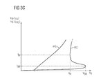
- FIG. 3C is a schematic diagram showing I/V characteristics of a switching device and a rectifying device of an electric assembly according to an embodiment with the desaturation I/V characteristic of the switching device under reverse bias showing a significant snap back.
- FIG. 4A is a schematic diagram showing the I/V characteristics of a switching device and a rectifying device of an electric assembly according to an embodiment with the diode I/V characteristic of the rectifying device showing a cut-in voltage.
- FIG. 4B is a schematic diagram showing the I/V characteristics of a switching device and a rectifying device of an electric assembly according to an embodiment with the diode I/V characteristic of the rectifying device intersecting the desaturation I/V characteristic of the switching device.
- FIG. 5A is a schematic circuit diagram of an electric assembly according to an embodiment including an RC-IGBT and a desaturation diode that includes a Schottky contact, an ohmic contact, or a gated channel.
- FIG. 5B is a schematic circuit diagram of an electric assembly according to an embodiment including an IGFET and a desaturation diode that includes a Schottky contact, an ohmic contact, or a gated channel.
- FIG. 6 is a schematic circuit diagram of an electric assembly according to an embodiment including a control circuit.
- FIG. 7A includes a schematic vertical cross-sectional view of a portion of a desaturation diode on the basis of an SiC-MPS (merged pin Schottky) diode according to an embodiment and a schematic diagram illustrating the I/V characteristic of the desaturation diode under forward bias.
- SiC-MPS merged pin Schottky
- FIG. 7B includes a schematic vertical cross-sectional view of a desaturation diode on the basis of an MGD (MOS gated diode) according to an embodiment and a schematic diagram illustrating the I/V characteristic of the desaturation diode under forward bias.
- MGD MOS gated diode
- FIG. 7C includes a schematic vertical cross-sectional view of a portion of a desaturation diode on the basis of a TOPS (trench oxide pin Schottky) diode according to an embodiment and a schematic diagram illustrating the I/V characteristic of the desaturation diode under forward bias.
- TOPS trench oxide pin Schottky
- FIG. 7D includes a schematic vertical cross-sectional view of a portion of a desaturation diode on the basis of an IDEE (inverse-injection-dependency-of-emitter-efficiency) diode according to an embodiment and a schematic diagram illustrating the I/V characteristic of the desaturation diode under forward bias.
- IDEE inverse-injection-dependency-of-emitter-efficiency
- FIG. 8 is a schematic circuit diagram of an electric assembly according to an embodiment including a silicon RC-IGBT, an SiC desaturation diode, and an SiC clamping diode.
- FIG. 9A is a schematic plan view of a direct copper bonded board with an electric assembly according to an embodiment including a silicon RC-IGBT, an SiC desaturation diode, and an SiC clamping diode.
- FIG. 9B is a schematic plan view of a direct copper bonded board with an electric assembly according to another embodiment with a strip conductor forming a loop between a silicon RC-IGBT and an SiC desaturation diode.
- FIG. 10 is a schematic diagram of a half bridge circuit including SiC desaturation diodes parallel to silicon RC-IGBTs according to a further embodiment.
- FIG. 11 is a schematic diagram of a smart IGBT module including SiC desaturation diodes parallel to silicon RC-IGBTs according to a further embodiment.
- electrically connected describes a permanent low-ohmic connection between electrically connected elements, for example a direct contact between the concerned elements or a low-ohmic connection via a metal and/or highly doped semiconductor.
- electrically coupled includes that one or more intervening element(s) adapted for signal transmission may be provided between the electrically coupled elements, for example elements that are controllable to temporarily provide a low-ohmic connection in a first state and a high-ohmic electric decoupling in a second state.
- the Figures illustrate relative doping concentrations by indicating “ ⁇ ” or “+” next to the doping type “n” or “p”.
- n means a doping concentration which is lower than the doping concentration of an “n”-doping region while an “n+”-doping region has a higher doping concentration than an “n”-doping region.
- Doping regions of the same relative doping concentration do not necessarily have the same absolute doping concentration.
- two different “n”-doping regions may have the same or different absolute doping concentrations.
- FIGS. 1A to 1B refer to an electric assembly 500 that may form or may be part of a high-side switch or a low-side switch of a half-bridge circuit, wherein the half-bridge circuit may be part of a H-bridge, a motor controller or a switched-mode power converter, e.g., a DC/DC power converter, a DC/AC power converter, an AC/AC power converter, or an AC/DC converter.
- the electric assembly 500 may be a multilevel inverter, e.g., a multilevel NPC (neutral point clamped) inverter, or a PFC (power factor correction) converter.
- FIG. 1A shows the electric assembly 500 including a reverse conducting switching device 510 that includes an integrated body diode 519 .
- a load path of the switching device 510 is electrically connected between a first and a second load terminal L 1 , L 2 of the electric assembly 500 .
- first load terminal L 1 is at the supply side and may be electrically coupled to a power supply.
- the other one of the first and second load terminals L 1 , L 2 is at the load side and may be electrically coupled to a load to which the power supply supplies a load current through the electric assembly 500 .
- the switching device 510 includes transistor cells and may be an IGFET, for example an MOSFET (metal-oxide semiconductor field effect transistor) in the usual meaning including IGFETs with metal gates and/or with gates containing a semiconductor material such as heavily doped polycrystalline silicon. According to an embodiment the switching device 510 is an RC-IGBT. A control signal supplied through a control terminal CTR of the electric assembly 500 turns on and off the switching device 510 .
- IGFET for example an MOSFET (metal-oxide semiconductor field effect transistor) in the usual meaning including IGFETs with metal gates and/or with gates containing a semiconductor material such as heavily doped polycrystalline silicon.
- MOSFET metal-oxide semiconductor field effect transistor
- a rectifying device 560 is electrically connected to the first and second load terminals L 1 , L 2 .
- the rectifying device 560 is connected anti-parallel with respect to the switching device 510 and in parallel with the body diode 519 of the switching device 510 .
- the rectifying device 560 may be a freewheeling diode, by way of example.
- the rectifying device 560 and the switching device 510 are separated semiconductor devices in different housings and electrically connected through strip conductors and/or wiring bonds. Physical connections between a cathode terminal K of the rectifying device 560 and a collector terminal C of the switching device 510 and/or between an anode terminal A of the rectifying device 560 and an emitter terminal E of the switching device 510 may have an intrinsic, non-negligible effective inductance greater 0.1 nH.
- FIG. 1B shows a discrete inductive element 517 electrically connected between terminals of the switching device 510 and rectifying device 560 assigned to the second load terminal L 2 .
- the effective inductance may be at least 0.1 nH, for example, at least 1 nH or at least 10 nH.
- the switching device 510 When, starting from an off-state level, the control signal applied to the control terminal CTR rises above or falls below a turn-on threshold voltage, the switching device 510 turns on, wherein by field effect the transistor cells TC form gated channels that provide a low-resistive path between the first and the second load terminals L 1 , L 2 for a load current that flows through the switching device 510 and the load. The switching device 510 turns off when the control signal returns to the off-state level.
- the switching device 510 Under reverse bias of the electric assembly 500 , the switching device 510 is reverse biased.
- the body diode 519 of the switching device 510 is forward biased and conducts a reverse current I FRC of the switching device 510 .
- a datasheet of a reverse conductive switching device typically defines a nominal diode forward current I F as the maximum rating diode current for the reverse current I FRC up to which operation of the switching device 510 is safe.
- the reverse current I FRC When all transistor cells of the switching device 510 are turned off, the reverse current I FRC is a bipolar current and corresponds to the diode forward current of the body diode 519 .
- the bipolar current generates a dense charge carrier plasma in a semiconductor portion of the switching device 510 . The denser the charge carrier plasma is, the lower is an ohmic reverse resistance R rev of the switching device 510 under reverse bias.
- FIG. 1B shows a saturation I/V characteristic 411 of the reverse biased switching device 510 , wherein the saturation I/V characteristic 411 results from the bipolar current in case all transistor cells including the transistor cells for desaturation are turned off.
- the saturation I/V characteristic 411 is the I/V characteristic of the saturated body diode 519 .
- the gated channels of the transistor cells for desaturation start to carry at least a portion of the reverse current I R through the electric assembly 500 .
- the transistor cells for desaturation may be some or all of the transistor cells that control the load current through the switching device 510 under forward bias or may be additional transistor cells that are not switched under forward bias.
- the gated channels of the transistor cells for desaturation may reduce the voltage drop across all or some of the pn junctions of the body diode 519 to below the built-in potential such that the concerned pn junctions stop injecting charge carriers.
- a fully bipolar current instead of a fully bipolar current, at least in portions of the semiconductor portions a unipolar current substitutes the bipolar current in the on-state of the transistor cells for desaturation. Since the injection of charge carriers along at least some of the pn junctions of the body diode 519 is suppressed, charge carrier plasma density drops and the electric resistance increases.
- the remaining current defines a desaturation I/V characteristic 412 of the reverse-biased switching device 510 as illustrated in FIG. 1B . Since the charge carrier plasma is less dense with respect to the saturated state, the desaturation I/V characteristic 412 is shifted to higher values of the reverse voltage V R for the same reverse current I FRC through the switching device 510 .
- the ohmic reverse resistance R rev is significantly greater than for the exclusively bipolar current and results in a higher voltage drop across the switching device 510 for the same reverse current I FRC through the switching device 510 and in a smaller reverse current I FRC at the same reverse voltage V R .
- a diode I/V characteristic 415 of the rectifying device 560 is schematically illustrated in FIG. 1B .
- the diode I/V characteristic 415 is a function of type, layout, dimensions as well as dopant gradients and dopant concentrations in the rectifying device 560 and can be tailored to the application.
- type, layout, dimensions, dopant gradients and dopant concentrations of the rectifying device 560 are defined such that for diode forward currents I FD of the rectifying device 560 up to at least the nominal diode forward current of the switching device 510 , e.g., up to at least twice or up to four times, the diode I/V characteristic 415 is on the left-hand side of the desaturation I/V characteristic of the switching device 510 .
- the rectifying device 560 carries the greater portion of the total reverse current I R through the electric assembly 500 during desaturation and the diode forward current I FD through the rectifying device 560 is greater than the reverse current I FRC through the reverse-biased switching device 510 .
- the concerned transistor cells for desaturation typically turn off again timely before commutation such that the switching device 510 safely blocks at the time commutation starts and critical circuit conditions can be avoided, for example, a short-circuit condition with both the high side and the low side switch of a half-bridge circuit being turned on.
- a unipolar current flows through the transistor cells for desaturation and a bipolar current may flow in regions without turned-on transistor cells to keep a reverse current flowing.
- charge carriers are also present in the semiconductor portion during desaturation.
- material, dimensions, layout, dopant concentrations and dopant gradients of the rectifying device 560 are tuned such that within the nominal operating range the diode I/V characteristic 415 intersects the saturation I/V characteristic 411 of the reverse biased switching device 510 .
- the rectifying device 560 takes most of the total reverse current I R at a lower reverse voltage V R than for a typical pn junction such that, for example, power consumption for open-circuit conditions and power conversion efficiency under low-load conditions can significantly be improved.
- the switching device 510 is designed with a significant snap-back in a range of a reverse current I FRC lower than a snap-back current I SB , wherein up to the snap-back current I SB the diode I/V characteristic 415 is on the left hand side of the desaturation I/V characteristic 412 of the reverse biased switching device 510 such that up to the snap-back current I SB the rectifying device 560 carries a greater portion of the total reverse current I R through the electric assembly 500 .
- the switching device 510 can be designed to allow for a significant snap-back, because the rectifying device 560 significantly attenuates or suppresses the effect of the snap-back on the application.
- the switching device 510 is an RC-IGBT
- p- and n-doped regions at the collector side may be optimized for a low ohmic reverse resistance R rev and a low on-state resistance R on and/or specific transistor cells designed for attenuating the snap-back effect can be omitted.
- the diode I/V characteristic 415 may be designed such that the voltage drop across the forward biased diode is always smaller than a maximum snap-back voltage V SB or snap-back hold voltage V H of the switching device 510 for a diode forward current I FD through the forward biased rectifying device 560 up to at least the nominal diode forward current I F , e.g., up to twice or up to four times the nominal diode forward current I F to avoid any snap-back of the reverse-biased switching device 510 .
- FIGS. 2A to 2E illustrate the effect of a desaturation period on the charge in a semiconductor portion 100 of an RC-IGBT 511 .
- a desaturation portion 611 of the semiconductor portion 100 includes first gated channels TC 1 , e.g., transistor cells for desaturation that turn on during a desaturation period.
- the first gated channels TC 1 may be dedicated desaturation cells that only turn on during desaturation or may include some of the transistor cells used for controlling a load current under forward bias.
- An injection portion 612 may exclusively include second gated channels TC 2 , e.g., transistor cells that do not turn on during desaturation and that keep the reverse current flowing through the switching device 510 .
- the second gated channels TC 2 may be transistor cells used for controlling a load current under forward bias.
- Charge carrier density is low in sections of the desaturation portion 611 close to the opposite first and second surfaces 101 , 102 of the semiconductor portion 100 , because in the on-state of the first gated channels TC 1 no bipolar current flows in the desaturation portion 611 , whereas charge carrier density remains high in the injection portion 612 .
- FIG. 2C shows the charge carrier distribution after actual start of commutation.
- the high reverse recovery charge results in a comparatively high commutation current, which is the source of high switching losses.
- FIG. 2D shows the total charge in the semiconductor portion 100 during and after desaturation.
- the total charge of the desaturated RC-IGBT 511 is about 50% of the charge of the saturated RC-IGBT 511 at the beginning of the desaturation period.
- the total charge again increases to about 60% of the saturated RC-IGBT 511 .
- the total charge may be even higher than at the nominal end of the desaturation period.
- FIG. 2E shows the charge Q des in the desaturation portion 611 of the RC-IGBT 511 , Q inj shows the charge in the injection portion 612 and Q tot shows the total charge in the semiconductor portion 100 at different points in time.
- the previously turned-on first gated channels TC 1 in the desaturation portion 611 suppressed injection in the desaturation portion 611 and a charge carrier plasma with a low amount of charges Q des has been established in the desaturation portion 611 .
- the contribution of the charge Q inj in the injection portion 612 is comparatively high.
- the rectifying device 560 may carry a great portion of the remaining reverse current I R during desaturation.
- the injection portion 612 carries only a small portion of the first current I R . Re-establishment of the charge carrier plasma after the end of the saturation starts from a lower level and may be hampered by stray inductance and/or additional discrete inductive elements in the connection lines to the switching device 510 . Further, the switching device 510 may be designed with only a small or with no injection portion 612 such that desaturation is effective in the complete semiconductor portion 100 . For example, all transistor cells used for controlling a load current under forward bias may be addressed during desaturation.
- FIG. 3A refers to an embodiment of the electric assembly 500 according to FIG. 1A .
- a diode I/V characteristic 415 of the rectifying device 560 is between the saturation I/V characteristic 411 and the desaturation I/V characteristic 412 of the switching device 510 at least for a range of a reverse current I FRC of the switching device 510 from I F /2 up to at least I F , e.g., up to 2*I F or up to 4*I F , wherein I F is the maximum rating for the diode forward current of the integrated body diode 519 at a predefined case temperature.
- the forward current I FD of the rectifying device 560 is greater than for the reverse-biased switching device 510 during desaturation for the complete nominal operating range of the switching device 510 such that only few charge carriers are injected into the semiconductor portion of the RC-IGBT 511 during desaturation and desaturation efficiency is high.
- the forward current I FD of the rectifying device 560 is lower than for the saturated reverse-biased switching device 510 for a range of I FRC from at least 0.1*I F to I F , e.g., from 0.3*I F up to at least 2*I F or up to 4*I F to exploit the high density charge carrier plasma of the saturated RC-IGBT 511 for the static RC mode.
- the rectifying device 560 is from a wide-bandgap material.
- the rectifying device 560 is an SiC (silicon carbide) diode that includes a unipolar portion with a unipolar Schottky contact, an ohmic contact, or a gated channel, and that includes a bipolar portion, wherein a first section of the diode I/V characteristic 415 in the nominal operating range is defined mainly by the unipolar portion and a second section of the diode I/V characteristic 415 is mainly defined by the bipolar portion.
- SiC silicon carbide
- the rectifying device 560 may be based on silicon carbide with an active area of less than 600 ⁇ m, wherein a thickness of a low-doped drift zone of the rectifying device 560 may be in a range from 4 ⁇ m to 60 ⁇ m.
- the rectifying device 560 By designing the rectifying device 560 to exhibit a diode I/V characteristic 415 between the saturation and desaturation I/V characteristics 411 , 412 of the reverse-biased switching device 510 , a reverse current I FRC in the switching device 510 during desaturation is only a small portion of the total reverse current I R and only few charge carriers are present in the switching device 510 at the end of the desaturation period.
- Desaturation efficiency is significantly improved compared to electric assemblies with rectifying devices 560 having an I/V characteristic intersecting the desaturation I/V characteristic 412 of the switching device 510 within the nominal operating range, because reestablishment of the charge carrier plasma starts from a significantly lower level.
- the more efficient desaturation may either result in that a safety period between end of desaturation and start of commutation is increased and/or in that switching losses are reduced.
- the diode I/V characteristic 415 of the rectifying device 560 of the electric assembly 500 of FIG. 1A intersects the saturation I/V characteristic 411 of the reverse-biased switching device 510 at a threshold voltage V X2 .
- the forward current I FD through the rectifying device 560 is greater than the reverse current I FRC through the saturated reverse-biased switching device 510 .
- the forward current I FD through the rectifying device 560 is lower than the reverse current I FRC of the saturated reverse biased switching device 510 .
- a set-in voltage V SD of the rectifying device 560 is lower than a set-in voltage V SRC of the body diode 519 , e.g., the rectifying device 560 may include a Schottky contact with a set-in voltage V SD lower than the set-in voltage V SRC of a silicon pn junction of the body diode 519 of the switching device 510 .
- the electric assembly 500 allows a reverse current flow at low reverse voltage V R .
- the rectifying device 560 includes an ohmic contact, a gated channel, or a Schottky contact with a set-in voltage V SD of at most 0.6 V, e.g., a Schottky contact with a molybdenum/silicon carbide barrier.
- the voltage drop across the electric assembly 500 rises above the set-in voltage V SRC of the body diode 519 such that the body diode 519 of the switching device 510 takes an increasing portion of the total reverse current I R .
- the reverse current I R is evenly split between the reverse current I FRC through the saturated reverse-biased switching device 510 and the forward current I FD through the rectifying device 560 .
- the desaturation I/V characteristic of the reverse-biased switching device 510 shows a significant snap-back with a maximum snap-back voltage V SB and a snap-back hold voltage V H , which is the minimum voltage across the reverse biased switching device 510 when the reverse current I FRC further increases after the snap-back.
- the reverse current I FRC at the hold voltage V H defines a hold current I H .
- the rectifying device 560 may be designed such that in a range of the diode forward current I FD from 0 to the hold current hi the diode forward current I FD through the rectifying device 560 is significantly greater, for example, at least two times or at least ten times greater than the reverse current I FRC of the desaturated reverse-biased switching device 510 .
- the hold current I H is defined at the hold voltage V H , which is the minimum voltage drop across the reverse biased switching device 510 after snap-back.
- V H the hold voltage
- the rectifying device 560 takes most of the current for a current range in which the desaturated reverse-biased switching device 510 shows the snap-back, the effect of the snap-back on the application is low.
- RC-IGBTs are designed to minimize a snap-back effect on the costs of other device parameters, such as, for example on-state resistance, thermal resistance of the body diode, avalanche ruggedness and/or low reverse recovery charge
- design constraints aiming at suppressing a snap-back behavior can be neglected such that there is more room for an improved trade-off as regards the other constraints.
- all transistor cells may be used for desaturation and the switching device 510 includes only one type of transistor cells which can be controlled in the same way.
- the rectifying device 560 is designed such that at least for a reverse current I FRC up to the nominal diode forward current I F of the reverse biased switching device 510 , e.g., up to twice or up to four times the nominal diode forward current I F , the diode forward current I FD through the forward biased rectifying device 560 is higher than the hold current I H .
- the RC-IGBT is safe from a snap-back during which the RC-IGBT changes to a bipolar mode.
- the bipolar mode would cause current filaments. Due to the positive temperature efficient current filaments may result in locally increased current densities which may irreversible damage the lattice of the semiconductor material.
- the rectifying device 560 conducts a forward current only for the desaturation period, which is a partial period of the off-time of the electric assembly 500 , or if the reverse current I R is low, overall power consumption in the rectifying device 560 is low and the active area of the rectifying device 560 can be small. Small, cost-effective SiC diodes may be used to significantly improve the efficiency of low-cost silicon RC-IGBTs.
- FIG. 4A refers to an embodiment of the electric assembly 500 of FIG. 1A with a rectifying device 560 with a unipolar portion dominating the diode I/V characteristic 415 below a cut-off voltage V X1 and below a cut-off diode forward current I X1 .
- a bipolar portion gets more dominant and supersedes or superimposes to the I/V characteristic of the unipolar portion.
- V R greater than V X1
- the slope of the diode I/V characteristic is significantly steeper than for reverse voltages V R below the cut-off voltage V X1 .
- the cut-off voltage V X1 is higher than a voltage drop V X1@sat across the switching device in the saturated mode with the transistor cells for desaturation turned off and lower than a voltage drop V X1@des across the desaturating switching device 510 with the transistor cells for desaturation turned on at I FRC equal to I FD , respectively.
- layout, dimensions, dopant concentration and dopant gradients in the rectifying device 560 are selected such that the cut-off current I X1 is between 0.1*I F and I F , e.g., between 0.1*I F and 2*I F and at the cut-off current I X1 the voltages across the saturated and the desaturated reverse biased switching device 510 hold a distance of at least 200 mV, 500 mV, 1V or 2V to the cut-off voltage V X1 such that the diode I/V characteristic 415 can meet all conditions as outlined for FIGS. 3A to 3C in combination.
- the unipolar portion may include a Schottky contact, an ohmic contact, a gated channel, or any combination thereof.
- the diode I/V characteristic 415 a at 25° C. has a cut-off voltage V Xa at 25° C. close to the voltage drop across the reverse biased switching device with the transistor cells TC for desaturation turned on such that the diode I/V characteristic 415 a at 25° C. intersects the desaturation I/V characteristic 412 of the switching device at a reverse current through the switching device below the nominal diode forward current I F , e.g., below twice or below four times the nominal diode forward current I F .
- Both the reverse biased switching device 510 and the forward biased rectifying device 560 can contribute to conveying a high pulse current or an overload condition of the application.
- the rectifying device 560 is a SiC diode and includes a unipolar portion and a bipolar portion. Rectifying devices based on silicon carbide show a strong temperature dependency.
- FIG. 4B shows a diode IN characteristic 415 b for a case temperature of, e.g., 175° C.
- the cut-off voltage V x1 may decrease with increasing temperature such that the diode I/V characteristic 415 b intersects the desaturation I/V characteristic 412 of the reverse-biased switching device 510 before the temperature of the rectifying device 560 exceeds a critical temperature.
- the switching device 510 takes a portion of the current through the rectifying device 560 such that the rectifying device 560 does not heat up further.
- the rectifying device 560 for example, a SiC desaturation diode may be provided with only a low safety margin such that a low-cost SiC diode with small active area can be used.
- the SiC diode is safe from being destroyed, because the electric assembly 500 falls in a safety mode that results from that the switching device 510 , which typically is defined with great safety margins, takes most of the current.
- the electric assembly 500 illustrated in FIG. 5A includes an RC-IGBT 511 , e.g., an Si-RCDC (silicon RC-IGBT with diode control) and a rectifying device 560 electrically arranged anti-parallel to the RC-IGBT 511 .
- the rectifying device 560 is effective as auxiliary diode that increases efficiency of desaturation of the reverse biased RC-IGBT 511 , improves low-current conductivity of the reverse-biased electric assembly 500 , and/or attenuates the effect of snapback in the reverse-biased RC-IGBT 511 on the circuit environment.
- a collector terminal C of the RC-IGBT 511 forms or is electrically connected to the first load terminal L 1
- an emitter terminal E forms or is electrically connected to the second load terminal L 2
- a gate terminal G forms or is electrically coupled or connected to the control terminal CTR of the electric assembly 500 .
- the RC-IGBT 511 integrates a body diode 519 which is spatially merged with transistor cells of the RC-IGBT 511 .
- a control signal applied to the gate terminal G turns on and off the transistor cells of the RC-IGBT 511 .
- a cathode terminal of the rectifying device 560 is directly electrically connected to the first load terminal L 1 , to the collector electrode C or to both.
- An anode terminal A of the rectifying device 560 is directly electrically connected to the second load terminal L 2 , to the emitter electrode E or to both.
- a semiconductor portion of the rectifying device 560 may be based on silicon carbide SiC.
- the electric assembly 500 includes an IGFET 512 with integrated body diode 519 and a rectifying device 560 , wherein the rectifying device 560 is electrically arranged anti-parallel to the IGFET 512 and effective as auxiliary diode as described above.
- FIG. 6 shows an electric assembly 500 that includes an RC-IGBT 511 , a rectifying device 560 electrically arranged anti-parallel to the RC-IGBT 511 , and a control circuit 590 for controlling the RC-IGBT 511 .
- the rectifying device 560 is a diode, wherein type, layout, dimensions, dopant concentrations and dopant gradients are selected such that the diode IN characteristic fulfills at least one of the conditions as outlined above.
- a first control output OUT 1 of the control circuit 590 is electrically connected to the control input CTR of the electric assembly 500 .
- the electric assembly 500 may be or may be part of the low-side switch or of the high-side switch in a half-bridge circuit.
- the control circuit 590 may include a second control output OUT 2 for controlling a further electronic assembly that forms or that is part of the complementary switch in the half-bridge circuit.
- the control circuit 590 generates and outputs a control signal, e.g., a square signal at the first control output OUT 1 , wherein the level of the control signal controls the on and off periods of transistor cells of the RC-IGBT 511 under forward and under reverse bias. For example, a high level of the control signal close to VCC may turn on the RC-IGBT 511 and a low level of the control signal close to, e.g., GND or VEE may turn off the RC-IGBT 511 .
- a control signal close to VCC may turn on the RC-IGBT 511 and a low level of the control signal close to, e.g., GND or VEE may turn off the RC-IGBT 511 .
- control circuit 590 may generate and output a desaturation pulse of predefined duration at the end of a reverse bias cycle of the electric assembly 500 .
- the desaturation pulse is applied to the control input CTR of the electric assembly 500 at a predefined point in time before a bias across the electric assembly 500 changes from reverse to forward.
- the desaturation pulse turns on gated channels for desaturation, e.g., transistor cells provided only for desaturation or some or all of the transistor cells that control the load current under forward bias.
- the length of a desaturation pulse may depend on the switching frequency at which the control circuit 590 turns on and off the RC-IGBT 511 .
- a safety period between the end of the desaturation pulse and the predicted start of commutation including the change from reverse bias to forward bias may be in the range from some hundred nanoseconds up to several microseconds.
- the rectifying device 560 is a diode, wherein type, layout, dimensions, dopant concentrations and dopant gradients are selected such that the diode I/V characteristic fulfills at least one of the conditions as outlined above.
- the control circuit 590 may include further input terminals INP that allow a higher control instance, e.g., a processor circuit to control the control circuit 590 .
- One or more feedback terminals FB may receive a signal or signals descriptive for load and/or source conditions such that the control circuit 590 may adjust duty cycle and/or switching frequency of the electric assembly 500 to varying load or source conditions.
- FIGS. 7A to 7D refer to embodiments of the rectifying device 560 of FIG. 1A , wherein the rectifying device 560 includes a unipolar portion mainly defining a shallow section of the diode I/V characteristic 415 below or above a cut-in voltage V X1 and a bipolar portion mainly defining a steep section of the diode I/V characteristic 415 above or below the cut-in voltage V X1 .
- the shallow section of the diode I/V characteristic 415 may be dominated by unipolar current, e.g., through a Schottky contact, an ohmic contact or a gated channel.
- unipolar current e.g., through a Schottky contact, an ohmic contact or a gated channel.
- a bipolar current through a pn junction may supersede or may superimpose to the unipolar current.
- Semiconducting regions of the rectifying device 560 of FIG. 1A are formed in a semiconductor portion 100 that includes an anode structure 110 at a front side along a first surface 101 and a cathode structure 120 at a back side along a second surface 102 parallel to and opposite of the first surface 101 .
- a metal anode electrode 310 is electrically connected to and may form ohmic contacts with heavily doped anode zones 111 of the anode structure 110 at the front side.
- a metal cathode electrode 320 is directly connected to the cathode structure 120 at the back side.
- the cathode structure 120 includes a heavily doped contact portion 129 forming an ohmic contact with the metal cathode electrode 320 .
- a lightly doped drift zone 121 is formed between, e.g., may separate the contact portion 129 from the anode structure 110 and may form pn junctions pn 0 with the anode zones 111 .
- the semiconductor portion 100 may be from silicon, germanium, silicon carbide, gallium arsenide or gallium nitride, by way of example.
- FIG. 7A refers to an MPS diode 561 that includes separated anode zones 111 extending from the first surface 101 into the cathode structure 120 , e.g., into the drift zone 121 .
- the anode zones 111 may be stripe-shaped with one horizontal dimension significantly exceeding the second horizontal dimension orthogonal to the first horizontal dimension, may be dot-shaped with both horizontal dimensions within the same order of magnitude or may form a grid, e.g., a hexagonal grid. Between neighboring anode zones 111 channel portions 125 of the cathode structure 120 directly adjoin to the metal anode electrode 310 and form Schottky contacts SC with the metal anode electrode 310 .
- the metal anode electrode 310 may include Schottky contact portions 311 , which directly adjoin which includes or is from titanium (Ti), and a main portion 312 , which may include or may be from aluminum.
- the Schottky contact portions 311 directly adjoin the channel portions 125 and the main portion 312 forms ohmic contacts to the anode zones 111 .
- the Schottky contacts SC convey a unipolar forward current I RF .
- I RF With increasing diode forward current I RF , a voltage drop along the pn junctions pn 0 increases.
- the MPS diode 561 can be designed to fulfill at least two of the conditions described with reference to FIGS. 3A to 3C in combination.
- an MGD 562 includes anode zones 111 forming pn junctions pn 0 with the cathode structure 120 and further pn junction pn 1 with source zones 112 , wherein the anode zones 111 separate the source zones 112 from the cathode structure 120 .
- the source zones 112 are formed between the first surface 101 and the anode zones 111 .
- Trench gate structures extend from the first surface 101 to at least the cathode structure 120 .
- the trench gate structures include a gate electrode 118 , which is insulated from the semiconducting material of the semiconductor portion 100 , and a gate dielectric 119 that separates the gate electrode 118 at least from the anode zones 111 .
- the gate electrode 118 , the anode zones 111 and the source zones 112 are electrically connected through low-ohmic connections and/or through the metal anode electrode 310 , which may be formed along the first surface 101 .
- any current flow through the anode zones 111 may reduce the potential in the anode zones 111 to below the potential of the metal anode electrode 310 and a positive potential difference may build up between the gate electrode 118 and the anode zones 111 despite that the gate electrode 118 and the anode zones 111 are directly connected to the metal anode electrode 310 .
- the potential difference increases with increasing current flow through the anode zones 111 such that above a cut-in voltage V X1 inversion channels build up along the gate dielectric 119 through the anode zones 111 .
- the diode I/V characteristic 415 of the MGD 562 can be extremely steep between a built-in voltage of, e.g., 0.6 V and a cut-in voltage V X1 of, e.g., 2 V. Beyond the cut-in voltage V X1 the current flow is almost unipolar resulting in a shallow, approximately linear increase of the diode reverse current I RF .
- the diode I/V characteristic 415 of the MGD 562 can be designed to fulfill at least the conditions for the low-current operation mode as discussed in FIG. 3B .
- FIG. 7C refers to a TOPS diode 563 .
- the anode structure 110 includes conductive plugs 117 , e.g., doped polysilicon plugs extending from the first surface 101 into the drift zone 121 and forming ohmic contacts with a main portion 312 of the metal anode electrode 310 .
- Insulator structures 116 line vertical sidewalls of the conductive plugs 117 .
- the anode zones 111 are formed in the vertical projection of the conductive plugs 117 .
- the insulator structures 116 prevent the diffusion of p-type dopants in a lateral direction and facilitate the formation of the anode zones 111 in a distance to the first surface 101 .
- Channel portions 125 of the cathode structure 120 form Schottky contacts SC with Schottky contact portions 311 of the metal anode electrode 310 between neighboring conductive plugs 117 . Due to the lower set-in voltage V SD of the Schottky contacts SC, at first a unipolar forward current flows under forward bias. With increasing forward current a voltage drop along the pn junctions pn 0 increases and may finally trigger charge carrier injection along the pn junctions pn 0 at a cut-in voltage V X1 .
- channel portions 125 of the cathode structure 120 extend between the anode zones 111 and form unipolar homojunctions with heavily doped channel contact zones 112 that form ohmic contacts with the metal anode electrode 310 .
- Dopant concentrations and dimensions of both the anode zones 111 and the channel portions 125 may be selected such that an electric field fully depletes the channel portions 125 from mobile charge carriers under reverse bias such that reverse leakage current is low.
- the ohmic contacts of the channels 138 convey a bipolar current.
- a voltage drop along the pn junctions pn 0 between the drift zone 121 and the anode zones 111 increases.
- V X1 a cut-in voltage at which the voltage drop along the pn junctions pn 0 exceeds the set-in voltage of the pn junctions pn 0 , i.e., the specific built-in potential of the pn junctions pn 0
- an additional current through the forward biased pn junctions gradually adds to the current through the ohmic contacts such that the diode I/V characteristic 415 gets steeper with increasing forward current. Due to the ohmic nature, the IDEE conducts a low reverse current at low reverse voltage such that losses for low-current operation are low.
- the electric assembly 500 includes a clamping diode 515 with a breakdown voltage lower than a breakdown voltage of an auxiliary diode used as rectifying device 560 and lower than a breakdown voltage of the body diode 519 of the RC-IGBT 511 .
- An overvoltage condition triggers an avalanche breakdown only in the clamping diode 515 such that the clamping diode 515 may protect the RC-IGBT 511 and the rectifying device 560 against overvoltage.
- the clamping diode 515 may be designed for high avalanche ruggedness such that design constraints for the auxiliary diode are relaxed in this respect.
- Both the clamping diode 515 and the auxiliary diode may be diodes showing a cut-in voltage V X1 .
- both the clamping diode 515 and the auxiliary diode may be SiC MPS diodes, wherein the avalanche breakdown in the clamping diode 515 generates electron/hole pairs such that the reverse current is high and the clamping diode 515 effectively protects the silicon RC-IGBT 511 against overvoltage.
- the electric assembly 500 may also include an inductive element 517 between terminals of the rectifying device 560 and the switching device 510 , for example between the anode terminal AF of the clamping diode 515 and the emitter terminal E of the RC-IGBT 511 .
- the inductive element 517 may be a portion of a bond wiring, a loop in a strip conductor or a discrete inductive element bridging a gap in a strip conductor between the anode terminal AF of the clamping diode 515 and the emitter terminal E of the RC-IGBT 511 .
- the inductive element 517 may delay a takeover of a reverse current from the rectifying device 560 to the RC-IGBT 511 after the desaturation cycle of the RC-IGBT 511 .
- the electric assemblies 500 illustrated in FIGS. 9A and 9B include a carrier board 599 , e.g., a PCB (printed circuit board) or DCB (directly copper bonding) board. At least a first conductor structure 591 and a second conductor structure 592 are formed on a mounting surface of the carrier board 599 .
- the first conductor structure 591 forms or is electrically connected to a first load terminal L 1 .
- the second conductor structure 592 forms or is electrically connected to a second load terminal L 2 .
- the first and second conductor structures 591 , 592 may be copper pads or copper strips.
- a silicon RC-IGBT 511 , a clamping diode 515 and an auxiliary diode effective as the rectifying device 560 of FIG. 1A are mounted, e.g., soldered or bonded side-by-side on the first conductor structure 591 , wherein the cathodes of the auxiliary diode and the clamping diode 515 as well as the collector of the silicon RC-IGBT 511 directly contact the first conductor structure 591 .
- Bond wirings 586 electrically connect the exposed anode terminal AF of the clamping diode 515 and the exposed anode terminal A of the auxiliary diode with the second conductor structure 592 .
- the inductance of the bond wiring 586 between the desaturation diode and the second conductor structure 592 may be increased by reducing the number of bond wires in the bond wiring 586 between the desaturation diode and the second conductor structure 592 , by lengthening the bond wires or by forming the bond wires from another material.
- the increased inductance may further delay the recovery of the charge carrier plasma after desaturation.
- a loop 587 in the second conductor structure 592 between the silicon RC-IGBT 511 and the rectifying device 560 may increase the stray inductance between the desaturation diode and the silicon RC-IGBT.
- FIG. 10 refers to a portion of an electronic assembly 600 that may be a motor drive, a switched mode power supply, a primary stage of a switched mode power supply, a synchronous rectifier, a primary stage of a DC/AC converter, a secondary stage of a DC/AC converter, a primary stage of a DC/DC converter, or a portion of a solar power converter, by way of example.
- the electronic assembly 600 may include two identical electric assemblies 500 as described above arranged as low-side switch and high-side switch in a half-bridge configuration.
- the electric assemblies 500 may include silicon RC-IGBTs 511 with body diodes 519 and anti-parallel rectifying devices 560 effective as auxiliary diodes as described above.
- the load paths of the two electric assemblies 500 are electrically connected in series between a first supply terminal A and a second supply terminal B.
- the supply terminals A, B may supply a DC (direct-current) voltage or an AC (alternating-current) voltage.
- An intermediate network node NN between the two electric assemblies 500 may be electrically connected to an inductive load LD, which may be a winding of a transformer or a motor winding, or to a reference potential of an electronic circuit, by way of example.
- the electronic assembly 600 may be a motor drive with the electric assemblies 500 electrically arranged in a half-bridge configuration, the network node NN electrically connected to a motor winding and the supply terminals A, B supplying a DC voltage.
- the electronic assembly 600 may be a primary side stage of a switched mode power supply with the supply terminals A, B supplying an AC voltage of an input frequency to the electronic assembly 600 .
- the network node NN is electrically connected to a primary winding of a transformer.
- the electronic assembly 600 may be a synchronous rectifier of a switched mode power supply with the supply terminals A, B connected to a secondary winding of the transformer and the network node NN electrically connected to a reference potential of an electronic circuit at the secondary side of the switched mode power supply.
- the electronic assembly 600 may be a primary side stage of a DC/DC converter, e.g., a power optimizer or a micro-inverter for applications including photovoltaic cells with the supply terminals A, B supplying a DC voltage to the electronic assembly 600 and the network node NN electrically connected to an inductive storage element.
- a DC/DC converter e.g., a power optimizer or a micro-inverter for applications including photovoltaic cells with the supply terminals A, B supplying a DC voltage to the electronic assembly 600 and the network node NN electrically connected to an inductive storage element.
- the electronic assembly 600 may be a secondary side stage of a DC/DC converter, e.g., a power optimizer or a micro-inverter for applications including photovoltaic cells, wherein the electronic assembly 600 supplies an output voltage to the supply terminals A, B and wherein the network node NN is electrically connected to the inductive storage element.
- a DC/DC converter e.g., a power optimizer or a micro-inverter for applications including photovoltaic cells
- FIG. 11 refers to an IGBT module 700 including the electronic assembly 600 of FIG. 10 .
- the IGBT module 700 may further include a gate control circuit 710 configured to supply a control signal for alternately switching on and off the electronic assembly 600 and a gate driver 720 controlled by the gate control circuit 710 and electrically connected to gate terminals of the electronic assembly 600 .
Landscapes
- Engineering & Computer Science (AREA)
- Microelectronics & Electronic Packaging (AREA)
- Power Engineering (AREA)
- Physics & Mathematics (AREA)
- Condensed Matter Physics & Semiconductors (AREA)
- General Physics & Mathematics (AREA)
- Computer Hardware Design (AREA)
- Ceramic Engineering (AREA)
- Dc-Dc Converters (AREA)
- Inverter Devices (AREA)
- Power Conversion In General (AREA)
Applications Claiming Priority (3)
| Application Number | Priority Date | Filing Date | Title |
|---|---|---|---|
| DE102016109235 | 2016-05-19 | ||
| DE102016109235.5 | 2016-05-19 | ||
| DE102016109235.5A DE102016109235B4 (de) | 2016-05-19 | 2016-05-19 | Elektrische baugruppe, die eine rückwärts leitende schaltvorrichtung und eine gleichrichtende vorrichtung enthält |
Publications (2)
| Publication Number | Publication Date |
|---|---|
| US20170338815A1 US20170338815A1 (en) | 2017-11-23 |
| US10200028B2 true US10200028B2 (en) | 2019-02-05 |
Family
ID=60255166
Family Applications (1)
| Application Number | Title | Priority Date | Filing Date |
|---|---|---|---|
| US15/497,290 Active US10200028B2 (en) | 2016-05-19 | 2017-04-26 | Electric assembly including a reverse conducting switching device and a rectifying device |
Country Status (2)
| Country | Link |
|---|---|
| US (1) | US10200028B2 (de) |
| DE (1) | DE102016109235B4 (de) |
Cited By (2)
| Publication number | Priority date | Publication date | Assignee | Title |
|---|---|---|---|---|
| US20170054383A1 (en) * | 2014-05-01 | 2017-02-23 | Schneider Electric It Corporation | Power supply control |
| US11398769B2 (en) * | 2018-02-23 | 2022-07-26 | Rohm Co., Ltd. | Semiconductor device comprising switching elements and capacitors |
Families Citing this family (9)
| Publication number | Priority date | Publication date | Assignee | Title |
|---|---|---|---|---|
| DE102015111371B4 (de) * | 2015-07-14 | 2017-07-20 | Infineon Technologies Ag | Halbleiterbauelement mit einem schaltbaren und einem nicht schaltbaren Diodengebiet |
| DE102017103111A1 (de) * | 2017-02-16 | 2018-08-16 | Semikron Elektronik Gmbh & Co. Kg | Halbleiterdiode und elektronische Schaltungsanordnung hiermit |
| WO2019060392A1 (en) * | 2017-09-22 | 2019-03-28 | Huawei Technologies Co., Ltd. | HYBRID ELEVATOR CONVERTERS |
| CN108418402A (zh) * | 2018-01-31 | 2018-08-17 | 北京交通大学 | 一种应用rc-igbt的机车牵引变流器的电流阈值退饱和控制方法 |
| JP6934823B2 (ja) * | 2018-02-27 | 2021-09-15 | 三菱電機株式会社 | 3レベルiタイプインバータおよび半導体モジュール |
| DE102018114375A1 (de) * | 2018-06-15 | 2019-12-19 | Infineon Technologies Ag | Leistungselektronikanordnung |
| CN110707077A (zh) * | 2019-09-12 | 2020-01-17 | 华为技术有限公司 | 二极管分立器件、带旁路功能的电路及变换器 |
| CN113497613A (zh) * | 2020-04-03 | 2021-10-12 | 台达电子企业管理(上海)有限公司 | 复合开关电路结构 |
| CN112327125A (zh) * | 2020-09-30 | 2021-02-05 | 北京Abb电气传动系统有限公司 | 功率半导体器件结壳热阻状态监测方法、设备、存储介质 |
Citations (9)
| Publication number | Priority date | Publication date | Assignee | Title |
|---|---|---|---|---|
| US5696396A (en) | 1993-11-12 | 1997-12-09 | Nippondenso Co., Ltd. | Semiconductor device including vertical MOSFET structure with suppressed parasitic diode operation |
| US5737165A (en) * | 1996-02-08 | 1998-04-07 | Ilc Data Device Corporation | Apparatus for databus fault isolation |
| US6049108A (en) | 1995-06-02 | 2000-04-11 | Siliconix Incorporated | Trench-gated MOSFET with bidirectional voltage clamping |
| US7889174B2 (en) | 1997-12-03 | 2011-02-15 | Immersion Corporation | Tactile feedback interface device including display screen |
| US20140125293A1 (en) | 2012-10-31 | 2014-05-08 | Toshiba Schneider Inverter Corporation | Stored electric power discharging circuit for inverter |
| US20150109031A1 (en) | 2013-10-22 | 2015-04-23 | Abb Technology Ag | Rc-igbt with freewheeling sic diode |
| WO2015079762A1 (ja) | 2013-11-29 | 2015-06-04 | シャープ株式会社 | 整流装置 |
| US20150214856A1 (en) | 2012-08-10 | 2015-07-30 | Mitsubishi Electric Corporation | Three-level power converting apparatus |
| US9543389B2 (en) | 2013-12-11 | 2017-01-10 | Infineon Technologies Ag | Semiconductor device with recombination region |
-
2016
- 2016-05-19 DE DE102016109235.5A patent/DE102016109235B4/de active Active
-
2017
- 2017-04-26 US US15/497,290 patent/US10200028B2/en active Active
Patent Citations (9)
| Publication number | Priority date | Publication date | Assignee | Title |
|---|---|---|---|---|
| US5696396A (en) | 1993-11-12 | 1997-12-09 | Nippondenso Co., Ltd. | Semiconductor device including vertical MOSFET structure with suppressed parasitic diode operation |
| US6049108A (en) | 1995-06-02 | 2000-04-11 | Siliconix Incorporated | Trench-gated MOSFET with bidirectional voltage clamping |
| US5737165A (en) * | 1996-02-08 | 1998-04-07 | Ilc Data Device Corporation | Apparatus for databus fault isolation |
| US7889174B2 (en) | 1997-12-03 | 2011-02-15 | Immersion Corporation | Tactile feedback interface device including display screen |
| US20150214856A1 (en) | 2012-08-10 | 2015-07-30 | Mitsubishi Electric Corporation | Three-level power converting apparatus |
| US20140125293A1 (en) | 2012-10-31 | 2014-05-08 | Toshiba Schneider Inverter Corporation | Stored electric power discharging circuit for inverter |
| US20150109031A1 (en) | 2013-10-22 | 2015-04-23 | Abb Technology Ag | Rc-igbt with freewheeling sic diode |
| WO2015079762A1 (ja) | 2013-11-29 | 2015-06-04 | シャープ株式会社 | 整流装置 |
| US9543389B2 (en) | 2013-12-11 | 2017-01-10 | Infineon Technologies Ag | Semiconductor device with recombination region |
Non-Patent Citations (5)
| Title |
|---|
| M. Rahimo, et al.: "Characterization of a Silicon IGBT and Silicon Carbide MOSFET Cross-Switch Hybrid"; IEEE Transactions on Power Electronics, vol. 30, No. 9, Sep. 2015. |
| M. Rahimo, et al.: "The Cross Switch "XS" Silicon and Silicon Carbide Hybride Concept"; PCIM Europe 2015, 19.-21. May 19-21, 2015; Nuernberg, Deutschland. |
| S. Fichtner, et al.: "Electro-Thermal Simulations and Experimental Results on teh Surge Current Capability of 1200 V SiC MPS Diodes"; 8th International Conference on Integrated Power Electronics Systems (CIPS 2014), Feb. 25-27, 2014, Nuremberg-Berlin, Offenbach:VDE Verlag, 2014, S. 438-443. |
| S. Fichtner, et al.: "Electro-Thermal Simulations and Experimental Results on teh Surge Current Capability of 1200 V SiC MPS Diodes"; 8th International Conference on Integrated Power Electronics Systems (CIPS 2014), Feb. 25-27, 2014, Nuremberg—Berlin, Offenbach:VDE Verlag, 2014, S. 438-443. |
| X. Song, A. Q. Huang, "6.5kV FREEDM-Pair: Ideal High Power Switch Capitalizing on Si and SiC", EPE 2015 ECCE Europe. |
Cited By (3)
| Publication number | Priority date | Publication date | Assignee | Title |
|---|---|---|---|---|
| US20170054383A1 (en) * | 2014-05-01 | 2017-02-23 | Schneider Electric It Corporation | Power supply control |
| US10491137B2 (en) * | 2014-05-01 | 2019-11-26 | Schneider Electric It Corporation | Power supply control |
| US11398769B2 (en) * | 2018-02-23 | 2022-07-26 | Rohm Co., Ltd. | Semiconductor device comprising switching elements and capacitors |
Also Published As
| Publication number | Publication date |
|---|---|
| US20170338815A1 (en) | 2017-11-23 |
| DE102016109235A1 (de) | 2017-11-23 |
| DE102016109235B4 (de) | 2019-02-14 |
Similar Documents
| Publication | Publication Date | Title |
|---|---|---|
| US10200028B2 (en) | Electric assembly including a reverse conducting switching device and a rectifying device | |
| US11410989B2 (en) | Semiconductor device having overload current carrying capability | |
| US10333387B2 (en) | Electric assembly including a semiconductor switching device and a clamping diode | |
| US10367057B2 (en) | Power semiconductor device having fully depleted channel regions | |
| CN110061050B (zh) | 半导体器件和具有势垒区的绝缘栅双极型晶体管 | |
| CN110943125B (zh) | 半导体装置 | |
| EP2365532B1 (de) | Halbleitervorrichtung und Stromrichter damit | |
| JP2009159184A (ja) | フリーホイールダイオードとを有する回路装置、及び、ダイオードを用いた回路装置とそれを用いた電力変換器 | |
| EP3678190A1 (de) | Halbleiterbauelement | |
| US10886909B2 (en) | Electric assembly including an insulated gate bipolar transistor device and a wide-bandgap transistor device | |
| US10475909B2 (en) | Electric assembly including a bipolar switching device and a wide bandgap transistor | |
| JP2008186921A (ja) | 半導体装置 | |
| JP2010050307A (ja) | 半導体装置およびその製造方法 | |
| JP5135666B2 (ja) | 電力変換装置 | |
| US20180269872A1 (en) | Transistor device | |
| US20230275576A1 (en) | Semiconductor switching module with insulated gate bipolar transistor and unipolar switching device | |
| US5621229A (en) | Semiconductor device and control method | |
| Rahimo et al. | Realization of higher output power capability with the bi-mode insulated gate transistor (BIGT) | |
| CN110767651A (zh) | 功率半导体器件 | |
| US10950690B2 (en) | Power electronic arrangement | |
| US20220406928A1 (en) | Semiconductor device with diode chain connected to gate metallization | |
| Flores et al. | New generation of 3.3 kV IGBTs with monolitically integrated voltage and current sensors |
Legal Events
| Date | Code | Title | Description |
|---|---|---|---|
| AS | Assignment |
Owner name: INFINEON TECHNOLOGIES AG, GERMANY Free format text: ASSIGNMENT OF ASSIGNORS INTEREST;ASSIGNORS:LAVEN, JOHANNES GEORG;BABURSKE, ROMAN;BASLER, THOMAS;REEL/FRAME:042145/0975 Effective date: 20170424 |
|
| STCF | Information on status: patent grant |
Free format text: PATENTED CASE |
|
| MAFP | Maintenance fee payment |
Free format text: PAYMENT OF MAINTENANCE FEE, 4TH YEAR, LARGE ENTITY (ORIGINAL EVENT CODE: M1551); ENTITY STATUS OF PATENT OWNER: LARGE ENTITY Year of fee payment: 4 |