US10092992B2 - Polishing apparatus, polishing head, and retainer ring - Google Patents
Polishing apparatus, polishing head, and retainer ring Download PDFInfo
- Publication number
- US10092992B2 US10092992B2 US15/163,571 US201615163571A US10092992B2 US 10092992 B2 US10092992 B2 US 10092992B2 US 201615163571 A US201615163571 A US 201615163571A US 10092992 B2 US10092992 B2 US 10092992B2
- Authority
- US
- United States
- Prior art keywords
- ring
- retainer ring
- screw thread
- annular
- polishing
- Prior art date
- Legal status (The legal status is an assumption and is not a legal conclusion. Google has not performed a legal analysis and makes no representation as to the accuracy of the status listed.)
- Active, expires
Links
- 238000005498 polishing Methods 0.000 title claims abstract description 198
- 239000000758 substrate Substances 0.000 claims abstract description 37
- 238000003825 pressing Methods 0.000 claims description 13
- 239000012528 membrane Substances 0.000 description 16
- 239000007788 liquid Substances 0.000 description 12
- 230000007246 mechanism Effects 0.000 description 12
- 239000002002 slurry Substances 0.000 description 7
- 230000008878 coupling Effects 0.000 description 6
- 238000010168 coupling process Methods 0.000 description 6
- 238000005859 coupling reaction Methods 0.000 description 6
- 125000006850 spacer group Chemical group 0.000 description 5
- 239000000463 material Substances 0.000 description 4
- 238000005096 rolling process Methods 0.000 description 4
- 239000012530 fluid Substances 0.000 description 3
- 229910052751 metal Inorganic materials 0.000 description 3
- 239000002184 metal Substances 0.000 description 3
- 230000003252 repetitive effect Effects 0.000 description 3
- 239000004696 Poly ether ether ketone Substances 0.000 description 2
- JUPQTSLXMOCDHR-UHFFFAOYSA-N benzene-1,4-diol;bis(4-fluorophenyl)methanone Chemical compound OC1=CC=C(O)C=C1.C1=CC(F)=CC=C1C(=O)C1=CC=C(F)C=C1 JUPQTSLXMOCDHR-UHFFFAOYSA-N 0.000 description 2
- 239000000919 ceramic Substances 0.000 description 2
- 230000002093 peripheral effect Effects 0.000 description 2
- 229920002530 polyetherether ketone Polymers 0.000 description 2
- 239000011347 resin Substances 0.000 description 2
- 229920005989 resin Polymers 0.000 description 2
- 238000009423 ventilation Methods 0.000 description 2
- OKTJSMMVPCPJKN-UHFFFAOYSA-N Carbon Chemical compound [C] OKTJSMMVPCPJKN-UHFFFAOYSA-N 0.000 description 1
- 229920002943 EPDM rubber Polymers 0.000 description 1
- 229920000181 Ethylene propylene rubber Polymers 0.000 description 1
- 229910052782 aluminium Inorganic materials 0.000 description 1
- XAGFODPZIPBFFR-UHFFFAOYSA-N aluminium Chemical compound [Al] XAGFODPZIPBFFR-UHFFFAOYSA-N 0.000 description 1
- 230000008901 benefit Effects 0.000 description 1
- 229910052799 carbon Inorganic materials 0.000 description 1
- 230000000694 effects Effects 0.000 description 1
- 229920001971 elastomer Polymers 0.000 description 1
- 230000003028 elevating effect Effects 0.000 description 1
- 229920006351 engineering plastic Polymers 0.000 description 1
- 239000000696 magnetic material Substances 0.000 description 1
- 239000007769 metal material Substances 0.000 description 1
- 238000000034 method Methods 0.000 description 1
- 230000004048 modification Effects 0.000 description 1
- 238000012986 modification Methods 0.000 description 1
- 229910052755 nonmetal Inorganic materials 0.000 description 1
- 229920003225 polyurethane elastomer Polymers 0.000 description 1
- 230000008569 process Effects 0.000 description 1
- 230000000717 retained effect Effects 0.000 description 1
- 229920002379 silicone rubber Polymers 0.000 description 1
- 239000004945 silicone rubber Substances 0.000 description 1
- 229910001220 stainless steel Inorganic materials 0.000 description 1
- 239000010935 stainless steel Substances 0.000 description 1
- XLYOFNOQVPJJNP-UHFFFAOYSA-N water Substances O XLYOFNOQVPJJNP-UHFFFAOYSA-N 0.000 description 1
- 238000003466 welding Methods 0.000 description 1
Images


Classifications
-
- H—ELECTRICITY
- H01—ELECTRIC ELEMENTS
- H01L—SEMICONDUCTOR DEVICES NOT COVERED BY CLASS H10
- H01L21/00—Processes or apparatus adapted for the manufacture or treatment of semiconductor or solid state devices or of parts thereof
- H01L21/02—Manufacture or treatment of semiconductor devices or of parts thereof
- H01L21/04—Manufacture or treatment of semiconductor devices or of parts thereof the devices having potential barriers, e.g. a PN junction, depletion layer or carrier concentration layer
- H01L21/18—Manufacture or treatment of semiconductor devices or of parts thereof the devices having potential barriers, e.g. a PN junction, depletion layer or carrier concentration layer the devices having semiconductor bodies comprising elements of Group IV of the Periodic Table or AIIIBV compounds with or without impurities, e.g. doping materials
- H01L21/30—Treatment of semiconductor bodies using processes or apparatus not provided for in groups H01L21/20 - H01L21/26
- H01L21/302—Treatment of semiconductor bodies using processes or apparatus not provided for in groups H01L21/20 - H01L21/26 to change their surface-physical characteristics or shape, e.g. etching, polishing, cutting
- H01L21/304—Mechanical treatment, e.g. grinding, polishing, cutting
-
- B—PERFORMING OPERATIONS; TRANSPORTING
- B24—GRINDING; POLISHING
- B24B—MACHINES, DEVICES, OR PROCESSES FOR GRINDING OR POLISHING; DRESSING OR CONDITIONING OF ABRADING SURFACES; FEEDING OF GRINDING, POLISHING, OR LAPPING AGENTS
- B24B37/00—Lapping machines or devices; Accessories
- B24B37/27—Work carriers
- B24B37/30—Work carriers for single side lapping of plane surfaces
- B24B37/32—Retaining rings
-
- B—PERFORMING OPERATIONS; TRANSPORTING
- B24—GRINDING; POLISHING
- B24B—MACHINES, DEVICES, OR PROCESSES FOR GRINDING OR POLISHING; DRESSING OR CONDITIONING OF ABRADING SURFACES; FEEDING OF GRINDING, POLISHING, OR LAPPING AGENTS
- B24B37/00—Lapping machines or devices; Accessories
- B24B37/04—Lapping machines or devices; Accessories designed for working plane surfaces
- B24B37/07—Lapping machines or devices; Accessories designed for working plane surfaces characterised by the movement of the work or lapping tool
- B24B37/10—Lapping machines or devices; Accessories designed for working plane surfaces characterised by the movement of the work or lapping tool for single side lapping
- B24B37/105—Lapping machines or devices; Accessories designed for working plane surfaces characterised by the movement of the work or lapping tool for single side lapping the workpieces or work carriers being actively moved by a drive, e.g. in a combined rotary and translatory movement
- B24B37/107—Lapping machines or devices; Accessories designed for working plane surfaces characterised by the movement of the work or lapping tool for single side lapping the workpieces or work carriers being actively moved by a drive, e.g. in a combined rotary and translatory movement in a rotary movement only, about an axis being stationary during lapping
-
- B—PERFORMING OPERATIONS; TRANSPORTING
- B24—GRINDING; POLISHING
- B24B—MACHINES, DEVICES, OR PROCESSES FOR GRINDING OR POLISHING; DRESSING OR CONDITIONING OF ABRADING SURFACES; FEEDING OF GRINDING, POLISHING, OR LAPPING AGENTS
- B24B37/00—Lapping machines or devices; Accessories
- B24B37/11—Lapping tools
- B24B37/20—Lapping pads for working plane surfaces
-
- B—PERFORMING OPERATIONS; TRANSPORTING
- B24—GRINDING; POLISHING
- B24B—MACHINES, DEVICES, OR PROCESSES FOR GRINDING OR POLISHING; DRESSING OR CONDITIONING OF ABRADING SURFACES; FEEDING OF GRINDING, POLISHING, OR LAPPING AGENTS
- B24B37/00—Lapping machines or devices; Accessories
- B24B37/34—Accessories
-
- B—PERFORMING OPERATIONS; TRANSPORTING
- B24—GRINDING; POLISHING
- B24B—MACHINES, DEVICES, OR PROCESSES FOR GRINDING OR POLISHING; DRESSING OR CONDITIONING OF ABRADING SURFACES; FEEDING OF GRINDING, POLISHING, OR LAPPING AGENTS
- B24B47/00—Drives or gearings; Equipment therefor
- B24B47/10—Drives or gearings; Equipment therefor for rotating or reciprocating working-spindles carrying grinding wheels or workpieces
- B24B47/12—Drives or gearings; Equipment therefor for rotating or reciprocating working-spindles carrying grinding wheels or workpieces by mechanical gearing or electric power
-
- H—ELECTRICITY
- H01—ELECTRIC ELEMENTS
- H01L—SEMICONDUCTOR DEVICES NOT COVERED BY CLASS H10
- H01L21/00—Processes or apparatus adapted for the manufacture or treatment of semiconductor or solid state devices or of parts thereof
- H01L21/02—Manufacture or treatment of semiconductor devices or of parts thereof
- H01L21/04—Manufacture or treatment of semiconductor devices or of parts thereof the devices having potential barriers, e.g. a PN junction, depletion layer or carrier concentration layer
- H01L21/18—Manufacture or treatment of semiconductor devices or of parts thereof the devices having potential barriers, e.g. a PN junction, depletion layer or carrier concentration layer the devices having semiconductor bodies comprising elements of Group IV of the Periodic Table or AIIIBV compounds with or without impurities, e.g. doping materials
- H01L21/30—Treatment of semiconductor bodies using processes or apparatus not provided for in groups H01L21/20 - H01L21/26
- H01L21/302—Treatment of semiconductor bodies using processes or apparatus not provided for in groups H01L21/20 - H01L21/26 to change their surface-physical characteristics or shape, e.g. etching, polishing, cutting
- H01L21/306—Chemical or electrical treatment, e.g. electrolytic etching
- H01L21/30625—With simultaneous mechanical treatment, e.g. mechanico-chemical polishing
-
- H—ELECTRICITY
- H01—ELECTRIC ELEMENTS
- H01L—SEMICONDUCTOR DEVICES NOT COVERED BY CLASS H10
- H01L21/00—Processes or apparatus adapted for the manufacture or treatment of semiconductor or solid state devices or of parts thereof
- H01L21/02—Manufacture or treatment of semiconductor devices or of parts thereof
- H01L21/04—Manufacture or treatment of semiconductor devices or of parts thereof the devices having potential barriers, e.g. a PN junction, depletion layer or carrier concentration layer
- H01L21/34—Manufacture or treatment of semiconductor devices or of parts thereof the devices having potential barriers, e.g. a PN junction, depletion layer or carrier concentration layer the devices having semiconductor bodies not provided for in groups H01L21/0405, H01L21/0445, H01L21/06, H01L21/16 and H01L21/18 with or without impurities, e.g. doping materials
- H01L21/46—Treatment of semiconductor bodies using processes or apparatus not provided for in groups H01L21/428
- H01L21/461—Treatment of semiconductor bodies using processes or apparatus not provided for in groups H01L21/428 to change their surface-physical characteristics or shape, e.g. etching, polishing, cutting
- H01L21/463—Mechanical treatment, e.g. grinding, ultrasonic treatment
Definitions
- seal rings which seal a gap between the drive ring and the retainer ring, are disposed inside and outside the first screw thread and the second screw thread, respectively.
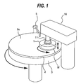
- the polishing head 1 is configured to be able to hold the wafer W on its lower surface by vacuum suction.
- the polishing head 1 and the polishing table 3 rotate in the same direction as indicated by arrows. In this state, the polishing head 1 presses the wafer W against the polishing surface 2 a of the polishing pad 2 .
- the polishing liquid is supplied from the polishing-liquid supply nozzle 5 onto the polishing pad 2 , so that the wafer W is polished by sliding contact with the polishing pad 2 in the presence of the polishing liquid.
Landscapes
- Engineering & Computer Science (AREA)
- Mechanical Engineering (AREA)
- Physics & Mathematics (AREA)
- Condensed Matter Physics & Semiconductors (AREA)
- General Physics & Mathematics (AREA)
- Manufacturing & Machinery (AREA)
- Computer Hardware Design (AREA)
- Microelectronics & Electronic Packaging (AREA)
- Power Engineering (AREA)
- Finish Polishing, Edge Sharpening, And Grinding By Specific Grinding Devices (AREA)
- Mechanical Treatment Of Semiconductor (AREA)
Applications Claiming Priority (6)
| Application Number | Priority Date | Filing Date | Title |
|---|---|---|---|
| JP2015-105793 | 2015-05-25 | ||
| JP2015105793 | 2015-05-25 | ||
| JP2016-007265 | 2016-01-18 | ||
| JP2016007265 | 2016-01-18 | ||
| JP2016096466A JP6449194B2 (ja) | 2015-05-25 | 2016-05-12 | 研磨装置、研磨ヘッド、およびリテーナリング |
| JP2016-096466 | 2016-05-12 |
Publications (2)
| Publication Number | Publication Date |
|---|---|
| US20160368115A1 US20160368115A1 (en) | 2016-12-22 |
| US10092992B2 true US10092992B2 (en) | 2018-10-09 |
Family
ID=57453372
Family Applications (1)
| Application Number | Title | Priority Date | Filing Date |
|---|---|---|---|
| US15/163,571 Active 2036-07-04 US10092992B2 (en) | 2015-05-25 | 2016-05-24 | Polishing apparatus, polishing head, and retainer ring |
Country Status (5)
| Country | Link |
|---|---|
| US (1) | US10092992B2 (zh) |
| KR (1) | KR101938936B1 (zh) |
| CN (1) | CN106181751B (zh) |
| SG (1) | SG10201604105TA (zh) |
| TW (1) | TWI656945B (zh) |
Cited By (2)
| Publication number | Priority date | Publication date | Assignee | Title |
|---|---|---|---|---|
| US20220111483A1 (en) * | 2020-10-14 | 2022-04-14 | Applied Materials, Inc. | Polishing head retaining ring tilting moment control |
| US11305399B2 (en) * | 2018-08-02 | 2022-04-19 | Ebara Corporation | Jig for a polishing apparatus |
Families Citing this family (7)
| Publication number | Priority date | Publication date | Assignee | Title |
|---|---|---|---|---|
| US10350722B2 (en) * | 2016-02-05 | 2019-07-16 | Toshiba Kikai Kabushiki Kaisha | Polishing apparatus |
| US10363647B2 (en) * | 2016-02-05 | 2019-07-30 | Toshiba Kikai Kabushiki Kaisha | Grinding tool |
| JP6894805B2 (ja) * | 2017-08-21 | 2021-06-30 | 株式会社荏原製作所 | 基板研磨装置および基板研磨装置における研磨液吐出方法 |
| JP7003838B2 (ja) * | 2018-05-17 | 2022-01-21 | 株式会社Sumco | 研磨ヘッド及びこれを用いたウェーハ研磨装置及び研磨方法 |
| JP6927617B1 (ja) * | 2020-11-19 | 2021-09-01 | 不二越機械工業株式会社 | ワーク研磨装置およびトップリング用樹脂マット体 |
| CN114734370B (zh) * | 2020-12-23 | 2023-06-30 | 中国科学院微电子研究所 | 一种抛光头和化学机械抛光设备 |
| CN114952610B (zh) * | 2021-11-10 | 2024-02-09 | 华海清科股份有限公司 | 一种用于化学机械抛光的承载头和抛光设备 |
Citations (9)
| Publication number | Priority date | Publication date | Assignee | Title |
|---|---|---|---|---|
| US6354927B1 (en) * | 2000-05-23 | 2002-03-12 | Speedfam-Ipec Corporation | Micro-adjustable wafer retaining apparatus |
| US20030070757A1 (en) * | 2001-09-07 | 2003-04-17 | Demeyer Dale E. | Method and apparatus for two-part CMP retaining ring |
| JP2003124169A (ja) | 2001-10-17 | 2003-04-25 | Tokyo Seimitsu Co Ltd | ウェーハ研磨装置 |
| US6840845B2 (en) * | 2001-11-19 | 2005-01-11 | Tokyo Seimitsu Co., Ltd. | Wafer polishing apparatus |
| KR20050067148A (ko) | 2002-10-02 | 2005-06-30 | 엥징게르 쿤츠토프테크놀러지 게베알 | 화학적 및 기계적 폴리싱장치의 반도체 웨이퍼 유지용고정링 |
| JP2008229790A (ja) | 2007-03-22 | 2008-10-02 | Nec Electronics Corp | リテーナリングおよび研磨装置 |
| JP2009190101A (ja) | 2008-02-13 | 2009-08-27 | Ebara Corp | 研磨装置 |
| US7622016B2 (en) | 2005-06-16 | 2009-11-24 | Will Be S & T Co., Ltd. | Retainer ring of chemical mechanical polishing device |
| KR20140052531A (ko) | 2012-10-24 | 2014-05-07 | 제타텍 주식회사 | 화학기계적 연마장치의 레테이너 링 |
Family Cites Families (1)
| Publication number | Priority date | Publication date | Assignee | Title |
|---|---|---|---|---|
| TWM435967U (en) * | 2012-04-27 | 2012-08-21 | Yau Yu Ind Co Ltd | Improved collet nut structure |
-
2016
- 2016-05-23 TW TW105115932A patent/TWI656945B/zh active
- 2016-05-23 SG SG10201604105TA patent/SG10201604105TA/en unknown
- 2016-05-24 US US15/163,571 patent/US10092992B2/en active Active
- 2016-05-24 KR KR1020160063304A patent/KR101938936B1/ko active IP Right Grant
- 2016-05-25 CN CN201610352162.0A patent/CN106181751B/zh active Active
Patent Citations (10)
| Publication number | Priority date | Publication date | Assignee | Title |
|---|---|---|---|---|
| US6354927B1 (en) * | 2000-05-23 | 2002-03-12 | Speedfam-Ipec Corporation | Micro-adjustable wafer retaining apparatus |
| US20030070757A1 (en) * | 2001-09-07 | 2003-04-17 | Demeyer Dale E. | Method and apparatus for two-part CMP retaining ring |
| JP2003124169A (ja) | 2001-10-17 | 2003-04-25 | Tokyo Seimitsu Co Ltd | ウェーハ研磨装置 |
| US6840845B2 (en) * | 2001-11-19 | 2005-01-11 | Tokyo Seimitsu Co., Ltd. | Wafer polishing apparatus |
| KR20050067148A (ko) | 2002-10-02 | 2005-06-30 | 엥징게르 쿤츠토프테크놀러지 게베알 | 화학적 및 기계적 폴리싱장치의 반도체 웨이퍼 유지용고정링 |
| US7622016B2 (en) | 2005-06-16 | 2009-11-24 | Will Be S & T Co., Ltd. | Retainer ring of chemical mechanical polishing device |
| JP2008229790A (ja) | 2007-03-22 | 2008-10-02 | Nec Electronics Corp | リテーナリングおよび研磨装置 |
| US7819723B2 (en) * | 2007-03-22 | 2010-10-26 | Nec Electronics Corporation | Retainer ring and polishing machine |
| JP2009190101A (ja) | 2008-02-13 | 2009-08-27 | Ebara Corp | 研磨装置 |
| KR20140052531A (ko) | 2012-10-24 | 2014-05-07 | 제타텍 주식회사 | 화학기계적 연마장치의 레테이너 링 |
Cited By (3)
| Publication number | Priority date | Publication date | Assignee | Title |
|---|---|---|---|---|
| US11305399B2 (en) * | 2018-08-02 | 2022-04-19 | Ebara Corporation | Jig for a polishing apparatus |
| US20220111483A1 (en) * | 2020-10-14 | 2022-04-14 | Applied Materials, Inc. | Polishing head retaining ring tilting moment control |
| US11623321B2 (en) * | 2020-10-14 | 2023-04-11 | Applied Materials, Inc. | Polishing head retaining ring tilting moment control |
Also Published As
| Publication number | Publication date |
|---|---|
| CN106181751B (zh) | 2019-08-13 |
| US20160368115A1 (en) | 2016-12-22 |
| KR101938936B1 (ko) | 2019-01-15 |
| TW201641215A (zh) | 2016-12-01 |
| KR20160138352A (ko) | 2016-12-05 |
| TWI656945B (zh) | 2019-04-21 |
| CN106181751A (zh) | 2016-12-07 |
| SG10201604105TA (en) | 2016-12-29 |
Similar Documents
| Publication | Publication Date | Title |
|---|---|---|
| US10092992B2 (en) | Polishing apparatus, polishing head, and retainer ring | |
| JP6867430B2 (ja) | 凹所およびキャップを有する、中心部が可撓性の片面研磨ヘッド | |
| US9403255B2 (en) | Polishing apparatus and polishing method | |
| US6857946B2 (en) | Carrier head with a flexure | |
| US11478895B2 (en) | Substrate holding device, substrate polishing apparatus, and method of manufacturing the substrate holding device | |
| TWI674171B (zh) | 基板保持裝置、研磨裝置、及研磨方法 | |
| US9815171B2 (en) | Substrate holder, polishing apparatus, polishing method, and retaining ring | |
| WO2017073318A1 (ja) | ウェーハ研磨装置およびこれに用いる研磨ヘッド | |
| JP6449194B2 (ja) | 研磨装置、研磨ヘッド、およびリテーナリング | |
| US20220048157A1 (en) | Substrate holding apparatus, elastic membrane, polishing apparatus, and method for replacing elastic membrane | |
| US20210060725A1 (en) | Elastic membrane and substrate holding apparatus | |
| US20210138606A1 (en) | Substrate holding apparatus and method of manufacturing a drive ring | |
| JP2017209757A (ja) | リテーナリング、基板保持装置及び基板研磨装置 | |
| KR101239372B1 (ko) | 리테이너 링의 유지 보수가 용이한 캐리어 헤드 | |
| US20160243670A1 (en) | Retainer ring, substrate holding apparatus, and polishing apparatus, and retainer ring maintenance method | |
| KR200488561Y1 (ko) | 직각도 조정에 의하여 밀착력이 향상되는 메커니컬 씰 | |
| KR20190000707U (ko) | 장착부의 고정력 및 가공성의 향상을 위한 메커니컬 씰 | |
| JP2007134478A (ja) | ウェーハ研磨装置及び方法 |
Legal Events
| Date | Code | Title | Description |
|---|---|---|---|
| AS | Assignment |
Owner name: EBARA CORPORATION, JAPAN Free format text: ASSIGNMENT OF ASSIGNORS INTEREST;ASSIGNORS:YASUDA, HOZUMI;FUKUSHIMA, MAKOTO;NABEYA, OSAMU;REEL/FRAME:038959/0300 Effective date: 20160530 |
|
| STCF | Information on status: patent grant |
Free format text: PATENTED CASE |
|
| MAFP | Maintenance fee payment |
Free format text: PAYMENT OF MAINTENANCE FEE, 4TH YEAR, LARGE ENTITY (ORIGINAL EVENT CODE: M1551); ENTITY STATUS OF PATENT OWNER: LARGE ENTITY Year of fee payment: 4 |