US10088522B2 - Apparatus and method for detecting faults in multilayer semiconductors - Google Patents
Apparatus and method for detecting faults in multilayer semiconductors Download PDFInfo
- Publication number
- US10088522B2 US10088522B2 US15/257,401 US201615257401A US10088522B2 US 10088522 B2 US10088522 B2 US 10088522B2 US 201615257401 A US201615257401 A US 201615257401A US 10088522 B2 US10088522 B2 US 10088522B2
- Authority
- US
- United States
- Prior art keywords
- mls
- target region
- electrical signal
- laser beam
- signal changes
- Prior art date
- Legal status (The legal status is an assumption and is not a legal conclusion. Google has not performed a legal analysis and makes no representation as to the accuracy of the status listed.)
- Active, expires
Links
Images


Classifications
-
- G—PHYSICS
- G01—MEASURING; TESTING
- G01R—MEASURING ELECTRIC VARIABLES; MEASURING MAGNETIC VARIABLES
- G01R31/00—Arrangements for testing electric properties; Arrangements for locating electric faults; Arrangements for electrical testing characterised by what is being tested not provided for elsewhere
- G01R31/28—Testing of electronic circuits, e.g. by signal tracer
- G01R31/302—Contactless testing
- G01R31/308—Contactless testing using non-ionising electromagnetic radiation, e.g. optical radiation
- G01R31/311—Contactless testing using non-ionising electromagnetic radiation, e.g. optical radiation of integrated circuits
-
- G—PHYSICS
- G01—MEASURING; TESTING
- G01R—MEASURING ELECTRIC VARIABLES; MEASURING MAGNETIC VARIABLES
- G01R1/00—Details of instruments or arrangements of the types included in groups G01R5/00 - G01R13/00 and G01R31/00
- G01R1/02—General constructional details
- G01R1/06—Measuring leads; Measuring probes
- G01R1/067—Measuring probes
- G01R1/07—Non contact-making probes
-
- G—PHYSICS
- G01—MEASURING; TESTING
- G01R—MEASURING ELECTRIC VARIABLES; MEASURING MAGNETIC VARIABLES
- G01R1/00—Details of instruments or arrangements of the types included in groups G01R5/00 - G01R13/00 and G01R31/00
- G01R1/30—Structural combination of electric measuring instruments with basic electronic circuits, e.g. with amplifier
-
- G—PHYSICS
- G01—MEASURING; TESTING
- G01R—MEASURING ELECTRIC VARIABLES; MEASURING MAGNETIC VARIABLES
- G01R31/00—Arrangements for testing electric properties; Arrangements for locating electric faults; Arrangements for electrical testing characterised by what is being tested not provided for elsewhere
- G01R31/26—Testing of individual semiconductor devices
-
- G—PHYSICS
- G01—MEASURING; TESTING
- G01R—MEASURING ELECTRIC VARIABLES; MEASURING MAGNETIC VARIABLES
- G01R31/00—Arrangements for testing electric properties; Arrangements for locating electric faults; Arrangements for electrical testing characterised by what is being tested not provided for elsewhere
- G01R31/28—Testing of electronic circuits, e.g. by signal tracer
- G01R31/2851—Testing of integrated circuits [IC]
-
- G—PHYSICS
- G01—MEASURING; TESTING
- G01R—MEASURING ELECTRIC VARIABLES; MEASURING MAGNETIC VARIABLES
- G01R31/00—Arrangements for testing electric properties; Arrangements for locating electric faults; Arrangements for electrical testing characterised by what is being tested not provided for elsewhere
- G01R31/28—Testing of electronic circuits, e.g. by signal tracer
- G01R31/302—Contactless testing
- G01R31/308—Contactless testing using non-ionising electromagnetic radiation, e.g. optical radiation
-
- H—ELECTRICITY
- H10—SEMICONDUCTOR DEVICES; ELECTRIC SOLID-STATE DEVICES NOT OTHERWISE PROVIDED FOR
- H10P—GENERIC PROCESSES OR APPARATUS FOR THE MANUFACTURE OR TREATMENT OF DEVICES COVERED BY CLASS H10
- H10P74/00—Testing or measuring during manufacture or treatment of wafers, substrates or devices
- H10P74/20—Testing or measuring during manufacture or treatment of wafers, substrates or devices characterised by the properties tested or measured, e.g. structural or electrical properties
- H10P74/207—Electrical properties, e.g. testing or measuring of resistance, deep levels or capacitance-voltage characteristics
-
- H—ELECTRICITY
- H10—SEMICONDUCTOR DEVICES; ELECTRIC SOLID-STATE DEVICES NOT OTHERWISE PROVIDED FOR
- H10P—GENERIC PROCESSES OR APPARATUS FOR THE MANUFACTURE OR TREATMENT OF DEVICES COVERED BY CLASS H10
- H10P74/00—Testing or measuring during manufacture or treatment of wafers, substrates or devices
- H10P74/20—Testing or measuring during manufacture or treatment of wafers, substrates or devices characterised by the properties tested or measured, e.g. structural or electrical properties
- H10P74/203—Structural properties, e.g. testing or measuring thicknesses, line widths, warpage, bond strengths or physical defects
Definitions
- Embodiments described herein relate generally to an apparatus and a method for detecting faults in multilayer semiconductors.
- ICs integrated circuits
- multilayer stacking has shown to be a promising economical and reliable way to increase the transistor density in ICs and, hence, increase their overall performance.
- flash memory manufactures have started to produce three-dimensional multilayer NAND flash chips that will enable solid-state drives (SSDs) to reach terabyte levels at reasonable costs in the foreseeable future. Therefore, three-dimensional multilayer semiconductor devices (MLS) are considered to be the most significant advancement of very-large-scale integration (VLSI), and they will be an essential technology in the semiconductor industry for decades to come.
- VLSI very-large-scale integration
- failure detection or identification of defect positions is an essential process for guaranteeing the reliability of the product and improving its yield. Therefore, failure detection techniques should be developed parallel to the advancements in semiconductor manufacturing.
- the first step to identify a fault in a defective chip is to determine its rough location (10 ⁇ 3 meter order) with a nondestructive technique, such as Lock-in Thermography (LIT).
- LIT Lock-in Thermography
- a more accurate nondestructive technique is used to detect the location of the fault (10 ⁇ 6 meter order) before proceeding to cut the chip to find the exact location of the fault (10 ⁇ 9 order) with a microscope, such as a Transmission Electron Microscope (TEM).
- Well-established accurate failure detection techniques include Laser Voltage Imaging (LVI) and Optical Beam Induced Resistance Change (OBIRCH).
- LVI is a technique based on the analysis of the reflected laser beam, which is usually reflected on the fir transistor layer; therefor LVI is not suitable to detect faults in deep layers of MLS.
- OBIRCH is a technique that directs an infrared laser beam onto the chip and measures the electrical resistance change caused by an increase of temperature; the laser-induced electrical resistance changes are significantly different for faulty locations than for functional locations.
- the infrared light is usually absorbed in the shallow transistor layers (or first layer for a single-laver semiconductor), the accumulated heat in these shallow layers is transported to the deep layer by heat conduction. This process results in an increase of temperature in the deep lavers where faults can exist, and if the temperature rise at a fault is high enough then anomalous electrical resistance changes in MLS could be detected, i.e., the fault location can be determined.
- FIG. 1 a schematic diagram showing an optical system and a controller system according to a first embodiment
- FIG. 2 is an illustration showing connections between components in the optical system and components in the controller system according to the first embodiment
- FIG. 3A is an upper-view schematic diagram of a multilayer semiconductor (MLS) according to the first embodiment
- FIG. 3B is a lateral-view schematic diagram of the MLS according to the first embodiment
- FIG. 4A is an illustration showing results of a numerical calculation according to the first embodiment
- FIG. 4B is an extended figure of an area R in FIG. 4A ;
- FIG. 5A is a lateral-view schematic diagram of the MLS in a misaligned case in the first embodiment
- FIG. 5B is a lateral-view schematic diagram of the MLS in an aligned case in the first embodiment
- FIG. 5C is an illustration showing an expected variation of electrical signal (without noise) measured as an irradiated zone is displaced along a position x;
- FIG. 6 is a flowchart of a beam alignment method according to the first embodiment
- FIG. 7 is a schematic diagram showing an optical system according to a second embodiment
- FIG. 8 is upper- and lateral-view schematic diagrams of the MLS according to the second embodiment.
- FIG. 9 is a flowchart of a beam alignment method according to the second embodiment.
- FIG. 10 is a schematic diagram showing an optical system according to a third embodiment
- FIG. 11 is upper- and lateral-view schematic diagrams of the MLS according to the third embodiment.
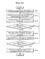
- FIG. 12 is a flowchart of a beam alignment method according to a third embodiment
- FIG. 13A is an upper-view schematic diagram of the MLS after expanding a laser beam according to the third embodiment
- FIG. 13B is an upper-view schematic diagram of the MLS before adjusting an interference pattern on the preselected target regions.
- FIG. 14 is a schematic diagram showing an optical system according to one variation of the third embodiment.
- heat may diffuse from the irradiated zone to its surroundings in a sphere-like manner, i.e., temperature drop is approximately directly proportional to the square of the distance from the center of the irradiated zone (heat source). Such temperature drop significantly decreases the possibility of detecting faults in deep layers due to very small anomalous electrical resistance changes.
- the precision of the measurement may decrease because heat diffuses both laterally and vertically, i.e., heat diffuses from the shallow layers to the deep layers but also along the layers. Therefore, this heat diffusion tends to flatten the temperature profile in deep layers resulting in an increase of the area where the fault is detected by the anomalous electrical resistance change, and the increase of this area decreases the precision of the measurement. This problem is more prominent as the location of the fault becomes deeper.
- an apparatus and method for determining the location and depth of faults and/or defects in a multilayer semiconductor (MLS) including determining the area of interest, where the fault is more likely to exist comprises a laser beam to selectively heat MLS, an optical system to direct the beam to preselected target regions in MLS, an amplifier to increase the thermally induced electrical signal change, and a computer system with controllers to control the foregoing setup and register the electrical signal changes obtained from MLS.
- this disclosure includes two methods for aligning the laser-induced irradiated zone (heat source) with the preselected target region, and one method for detecting the location of the fault in a MLS. The latter method also includes detecting the depth of the fault after locating it on the wider plane of MLS.
- FIG. 1 shows an arrangement of an optical system 100 and a controller system 101 according to the first embodiment.
- the optical system 100 is used to manipulate a laser beam 1 and comprises a laser source 40 , a polarizing plate 2 , a quarter-wave plate 9 , a beam splitter 5 , a camera 41 , an optical element 6 , a scanner 60 , a lens 4 , a lens 10 , a MLS 20 , a circuit board 30 , a stage 50 , and a stand 80 .
- the controller system 101 is used to control several elements in the optical system 100 and to record the electric, signal changes measured from the MLS 20 , and comprises an amplifier 130 , a laser controller 140 , a camera controller 141 , a stage controller 150 , a scanner controller 160 , and a computer system 170 .
- the laser beam 1 is generated with the laser source 40 .
- the laser beam 1 could pass through a polarizing plate 2 in order guarantee a desired linear polarization state; if the linear polarization state of the laser beam 1 is known just after exiting the laser source 40 , then the polarizing plate 2 could be omitted.
- the linear polarization state of the laser beam 1 could be changed to circular polarization with a quarter-wave plate 9 ; in this case the polarization angle of the incident laser beam 1 is adjusted to n/4 with respect to a virtual axis perpendicular to an optic axis, meanwhile an extraordinary axis of the quarter-wave plate 9 is parallel to the virtual axis.
- the laser beam 1 then passes through a beam splitter 5 , which can also be a polarizing beam splitter or any kind of prism (the beam splitter is later used to capture reflected or emitted light from the MLS 20 ).
- a beam splitter 5 which can also be a polarizing beam splitter or any kind of prism (the beam splitter is later used to capture reflected or emitted light from the MLS 20 ).
- the laser beam 1 then passes through the optical element 6 that is used to scan an irradiated zone on the MLS 20 .
- the optical element 6 can be a flat plate, a mirror, a lens, or any other element that can be used for scanning the laser beam 1 .
- the optical element 6 is manipulated with the scanner 60 , which in turn is manipulated with the scanner controller 160 that can comprise a Piezo element and/or a servo motor and/or a stepper motor and/or a linear motor.
- the laser beam 1 then passes through the lens 4 in order to be directed to the lens 10 and then to the MLS 20 .
- the lens 4 can be any one of, or a combination of, one or more concave lenses and/or one or more convex lenses and/or one or more objective lenses.
- the lens 10 can be a solid immersed lens (SIL) or any derivative in order to modify the numerical aperture of the optical system 100 .
- Equation (1) ⁇ is the diameter of the irradiated zone created by the incidence of the laser beam 1 on the shallow layers of the MLS 20 , ⁇ is a wavelength of the laser beam 1 , and NA is the numerical aperture of the optical system 100 .
- Equation (1) is formulated according to an ideal Airy disk intensity distribution on the shallow layers.
- the wavelength of the laser beam 1 is usually in the infrared region to reduce the absorption in a substrate 25 (see FIG. 3B ) of the MLS 20 .
- a NA and ⁇ in the optical system 100 should be selected according to a size of each of preselected target region, i.e., the size of the irradiated zone ⁇ should be around the same size as each of the preselected target regions.
- the MLS 20 is mounted on the circuit board 30 wherein different pins of peripherals of the MLS 20 are wired to the circuit board 30 .
- the circuit board 30 is used to apply a constant or variable voltage difference along one path in the MLS 20 or multiple paths in the MLS 20 , wherein these paths may include individual layers of the MLS 20 in order to detect a depth of each failure.
- the circuit board 30 is connected to the amplifier 130 , and this circuit board 3 C is fixed on the stage 50 .
- the stage 50 is used to control a spatial location of the MLS 20 in the optical system 100 ; the spatial location can be controlled in any of three Cartesian coordinates.
- the stage 50 is mounted on the stand 80 , which can comprise damping features in order to isolate the optical system 100 from external vibrations that can potentially affect measurement accuracy.
- a central component of the controller system 101 shown in FIG. 1 is the computer system 170 .
- the computer system 170 controls (i) switching of the laser beam 1 through the laser controller 140 , (ii) scanning of the laser beam 1 through the scanner controller 160 , (iii) switching and reading of/from the camera 41 through the camera controller 141 , and (iv) locating the MLS 20 in the optical system 100 through the stage controller 150 .
- the computer system 170 also controls voltage characteristics to be applied to the MLS 20 through the amplifier 130 ; the computer system 170 reads and registers amplified electrical signal change from the amplifier 130 .
- the electrical signal change is due to the electrical resistance change induced by a temperature increase in the MLS 20 .
- FIG. 2 shows an illustration showing connections between the components in the optical system 100 and the components in the controller system 101 .
- the optical system 100 can be built according to multiple arrangements, three of which are described as embodiments in this disclosure.
- FIG. 3A shows an upper view of a schematic diagram of a typical multilayer flash memory chip and an irradiated zone 1 a that is generated due to the incidence of the laser beam 1 onto a multilayer zone 26 .
- a typical multilayer flash memory structure is used as a general example of the MLS 20 ; however, the first embodiment and other embodiments described in this disclosure are applicable to detect faults in any MLS that has a periodic structure and whose structure comprises materials of different thermal conductivity.
- FIG. 3B shows a lateral view schematic diagram of the MLS 20 .
- An intensity of the irradiated zone la on a shallow layers 26 a of the MLS 20 is also shown in FIG. 3B , which corresponds to the upper view of the MLS 20 shown in FIG.
- a maximum irradiation location overlaps with a position of a preselected target region.
- the preselected target region corresponds to a vertical structure 22 that is visible in the upper view shown in FIG. 3A .
- the preselected target region was chosen because it consists of relatively high thermal conductivity material and it has a structure that extends from shallow layers 26 a to deep layers 26 b of the NILS 20 , as shown in FIG. 3B .
- a substrate layer 25 usually made of one material
- a bulk of a multilayer zone 26 made of multiple materials
- a bulk of circuit layers 27 made of multiple materials
- One of the preselected target regions may be a separator layer 22 for separating blocks of a multilayer flash memory chip.
- Such separator layer is typically made of a material with high thermal conductivity such as metal or alloy, and has a structure penetrating from shallow layers 26 a to deep layers 26 b of a MLS. Therefore, by heating a shallow part of the separator layer, it is possible to heat a deep part of the separator layer, and thereby, it is possible to effectively heat the deep layers of the MLS.
- the first embodiment is primarily directed to detect faults in the deep layers 26 b, but it can also detect faults in the shallow layers 26 a. Since infrared irradiation is highly absorbed by different materials in the circuit layers 27 , then the laser beam 1 is preferably directed through the substrate layer 25 , which is usually made of one material semi-transparent against the wavelength ⁇ of the laser beam 1 .
- FIG. 4A shows results of a numerical calculation that highlights two important advantageous effects of the first embodiment
- FIG. 4B is an extended figure of an area R in FIG. 4A
- FIGS. 4A and 4B Two advantageous effects of the first embodiment are highlighted in FIGS. 4A and 4B : one advantageous effect A is that a temperature of the deep layers 26 b in the MLS 20 is increased, and the other advantageous effect B is that a temperature of the shallow layers 26 a in the MLS 20 is decreased.
- the advantageous effect A indicates that by heating the preselected target region, the electric signal changes are amplified according to a temperature increase in the deep layers 26 b, when a voltage for generating a current is applied to MLS 20 .
- An amplified electric signal increases the sensitivity and/or accuracy of the measurement, as suggested in FIG. 5C , where the abscissa axis indicates the displacement x of the irradiated zone parallel to the vertical structures 22 and the ordinate axis indicates the electric signal or electric signal change. Therefore, the advantageous effect A results in an improvement of sensitivity and/or accuracy of the measurement for faults located in deep layers 26 b of a MLS.
- the advantageous effect B (as highlighted in FIG. 4A ) consists on a significant drop of temperature in the shallow layers 26 a. Therefore, we can further increase the power of the laser beam 1 without damaging the sample in the case where an electric signal read from the MLS 20 is to weak, e.g., the maximum and the minimum in FIG. 5C could be undetectable due to the noise. Therefore, a further more of power of the laser beam 1 , which is allowed by the advantageous effect B, would result in an improvement of the sensitivity and/or accuracy of the measurement for faults located in deep layers 6 b of a MLS.
- FIG. 5C shows that if the center of the irradiated zone is placed on the preselected target region, then the electrical signal becomes larger; in contrast, if the center of the irradiated zone between adjacent vertical structures 22 , then the electrical signal becomes weaker.
- the operator should have prior knowledge of the structure of the MLS 20 to judge whether the electric resistivity of the overly heated material is directly or inversely proportional to the temperature. For example, if the electric resistivity of the material of the vertical structures 22 were inversely proportional to the temperature, then the aligned configuration would correspond to the position where the electric resistivity is a minimum, i.e., according to Ohm's law the electrical signal becomes a maximum, as shown in FIG. 5C . Note that the noise in th electrical signal shown in FIG. 5C is omitted.
- the operator performs preparations that include, but are not limited to, fixing the optical elements on a frame of the optical system 100 , administrating power supply to the controller system 101 , adjusting a size of the irradiated zone to that of the preselected target region, and so forth.
- step S 201 the controller system 101 applies a constant or variable voltage through a selected circuit path of the MLS 20 .
- step S 202 the controller system 101 heats the shallow layers 26 a of the MLS 20 with the irradiated zone at a given location x.
- step S 203 the controller system 101 registers electrical signal or electrical signal changes inputted via the amplifier 130 .
- step S 204 the controller system 101 displaces the irradiated zone on the shallow layers 26 a of the MLS 20 .
- step S 205 the controller system 101 verifies whether scan of every scan path was finished.
- step S 202 When the scan was not finished, the controller system 101 returns to step S 202 .
- the controller system 101 proceeds to step S 206 .
- step S 206 the controller system 101 finds global minimum and maximum in the registered signals. Then proceed to step S 207 , the controller system 101 adjusts the position of the irradiated zone to match the position where the signal becomes minimum or maximum.
- the choice of whether to use the position where the signal becomes minimum or maximum as a position of a target region depends on the temperature dependence of an electric resistance of the material that composes the preselected region. If the target region is composed of a material that increases its thermal conductivity with increasing temperature, i.e., direct proportionality, then the aligned position would correspond to a minimum of the signal output.
- the aligned position would be a maximum of the signal output, as the case shown in FIG. 5C .
- step S 208 the controller system 101 adjusts the power intensity as to maximize the electric signal or electric signal change.
- This adjustment is optional and takes into consideration the advantageous effect B that allow an increase of the laser power without damaging the MLS 20 , as indicated in FIGS. 4A .
- the alignment of the first embodiment for scanning th MLS 20 to find the location if the possible fault is performed. Note that the scan is done along the structure of interest (i.e., the target regions) as shown in FIG. 3A and also shown in FIGS. 8 and 11 .
- the alternative noninvasive thermal-stimulation based apparatus and method capable of improving the manufacturing process and the yield of MLS by detecting the location of faults in deep layers of MLS, and/or detecting the depth of these faults. This would also allow the manufacturers to increase the number of layers of MLS and, hence, increase the functionality and performance of such devices.
- FIG. 7 An arrangement of an optical system according to the second embodiment is shown in FIG. 7 wherein a controller system and an observation system of the laser beam 1 are omitted and can correspond to the controller system 101 and an observation system constructed from the beam splitter 5 and the camera 41 shown in FIG. 1 . Furthermore, in the second embodiment, to the same structures as those of the first embodiment, the same reference numbers will be applied, and the redundant explanations thereof will be omitted.
- the optical system 200 is used to manipulate a laser beam 1 and comprises a laser source 40 , a polarizing plate 2 , a diffraction orating 7 , a convex lens 3 , a concave lens 8 , a solid immersion lens 10 , a MLS 20 , a circuit board 30 , a stage 50 , a stand 80 , and a scanner 60 .
- the lens 8 is used to redirect the laser beam 1 in scanning process.
- the lens 8 can be replaced with a plate and/or a mirror and/or any other element capable of scanning the laser beam 1 .
- the second embodiment has the diffraction grating 7 to increase the number of incident beams (i.e., diffracted laser beams) on the preselected target region in the MLS 20 .
- incident beams i.e., diffracted laser beams
- FIG. 8 As an upper- and lateral-view of the MLS 20 shown in FIG. 8 , by having such structure, it is possible to simultaneously heat multiple preselected target regions (i.e., the vertical structures 22 ) using the multiple diffracted laser beams 1 b , and thereby, an enhancement of the advantageous effects A and B (see FIGS. 4A and 4B ) becomes possible.
- a horizontal pitch of the diffracted laser beams 1 b must not necessarily match a distance between adjacent vertical structures 22 , the horizontal pitch should be a multiple of the distance between adjacent vertical structures 22 .
- the operator performs preliminarily preparations that include, but are not limited to, fixing the optical elements including the diffraction grating 7 on a frame of the optical system 200 , administrating power supply to the controller system 101 , adjusting sic of the irradiated zones to those of the preselected target regions, and so forth.
- the operator further performs a physical adjustment that includes, but is not limited to, rotating the diffraction orating 7 to adjust the horizontal pitch of the diffracted laser beams 1 b .
- a physical adjustment could be simply to change the diffraction grating 7 to obtain the desired pitch.
- Another physical adjustment could be to rotate the MLS 20 (manually or with the stage 50 ) while the diffraction grating 7 is fixed.
- step S 301 the controller system 101 applies a constant or variable voltage through a selected circuit path of the MLS 20 .
- step S 302 the controller system 101 heats the shallow layers 26 a of the MLS 20 with the irradiated zones.
- step S 303 the controller system 101 registers electrical signals or electrical signal changes inputted via the amplifier 130 .
- step S 304 the controller system 101 verifies whether the horizontal pitch between the diffracted laser beams 1 b matches a desired pitch. This verification may be done based on an image taken by the camera 41 . This verification could also be done through visual confirmation using a microscope or through reading the registered signal change while conducting the physical adjustment.
- step S 305 When the horizontal pitch between the diffracted laser beams 1 b matches the desired pitch, the controller system 101 determines that the adjustment of the horizontal pitch between the diffracted laser beams 1 b is finished (step S 305 ; YES), proceeds to step S 307 . On the other hand, when the horizontal pitch does not match the desired pitch, the controller system 101 determines that the adjustment of the horizontal pitch is not finished (step S 305 ; NO), conducts step S 306 , and returns to step S 302 .
- step S 306 a physical position of the diffraction grating 7 is adjusted so that the horizontal pitch between the diffracted laser beams 1 b matches the desired pitch. This adjustment may be done by the operator. If the optical system 200 has an attitude control system, or the like, of the diffraction grating 7 , the adjustment may be done by such system based on a control from the controller system 101 .
- step S 307 the controller system 101 finds global minimum and maximum in the registered signals. Then proceed to step S 308 , the controller system 101 fixes the physical positions of the MLS 20 and/or the diffraction grating 7 in order to overlap the irradiated zones with preselected target regions.
- step S 309 the controller system 101 adjusts the power intensity so as to maximize the electric signals or electric signal changes. This adjustment is optional as the first embodiment.
- step S 309 it i possible to set a lens that expands the irradiated zones along the preselected target regions, as for example shown in FIG. 8 with the ellipsoid-like beams. Not that the setting of he lens is optional and could also be incorporated in the alignment process for the first embodiment.
- FIG. 10 An arrangement of an optical system according to the third embodiment is shown in FIG. 10 wherein a controller system are omitted and can correspond to the controller system 101 shown in FIG. 1 . Furthermore, the third embodiment, to the same structures as those of the first or second embodiment, the same reference numbers will be applied, and the redundant explanations thereof will be omitted.
- the optical system 300 is used to manipulate a laser beam 1 and comprises a laser source 40 , a polarizing plate 2 , a concave lens 3 , convex lenses 4 a and 4 b, beam splitters 5 a and 5 b, a camera 41 , fixed mirrors 6 a and 6 b, adjustable (scanning) mirrors 7 a and 7 b, scanners 60 a and 60 b, a lens 10 , a MLS 20 , a circuit board 30 , a stage 50 , and a stand 80 .
- the mirrors 7 a and 7 b are used to redirect the laser beam 1 in scanning process.
- the function of the mirrors 7 a and 7 b could be replaced with a plate and/or a prism and/or any other element capable of scanning the laser beam 1 .
- FIG. 11 shows the upper and side view of the MLS 20 for the aligned heating configuration according to the third embodiment. Such heating configuration shown in FIG. 11 is reached after an alignment method of the third embodiment. The alignment method will be described in the following with reference to FIGS. 12, 13A and 13B .
- FIG. 12 shows an operation of the alignment method of the third embodiment.
- the operation shown in FIG. 12 is started after finishing the operation described in the first embodiment with reference to FIG. 6 .
- the laser beam 1 is first expanded to cover two or more preselected target region (i.e., two or more vertical regions 22 ) as shown in FIG. 13A .
- an area 1 c indicates an irradiated zone with the expanded laser beam 1 .
- step S 401 can be omitted.
- step S 402 the controller system 101 adjusts the mirror 7 a by driving the scanner 60 a via the scanner controller 160 in order to create an interference pattern and adjust a relative pitch and a position of fringes in the interference pattern.
- step S 403 the controller system 101 reads an image of the interference pattern from the camera 41 .
- step S 404 the controller system 101 determines, based on the obtained image, whether the relative pitch of the fringes is reached a target relative pitch. When the relative pitch is not reached the target relative pitch (step S 404 ; NO), the controller system 101 returns to step S 402 . On the other hand, when the relative pitch is reached the target relative pitch (step S 404 ; YES), the controller system 101 proceed to step S 405 .
- step S 404 the controller system may also determine whether the interference pattern includes a fringe passing through the center of a beam cross-section and whether the fringes are parallel to the preselected target regions.
- step S 404 there is a case where the fringes in the interference pattern are parallel to the preselected target regions but do not overlap with the preselected target regions, as shown in FIG. 13B .
- the same alignment process as the first embodiment could be conducted to obtained the aligned configuration shown in FIG. 11 .
- the controller system 101 heats the shallow layers 26 a of the MLS 20 with the irradiated zone. Then proceed to step S 406 , the controller system 101 registers electrical signals or electrical signal changes inputted via the amplifier 130 . Then proceed to step S 407 , the controller system 101 verifies whether the electrical signals or the electrical signal changes reach peaks.
- step S 407 When the electrical signals or the electrical signal changes do not reach the peaks (step S 407 ; NO), the controller system 101 returns to step S 402 . On the other hand, when the electrical signals or the electrical signal changes reach the peaks (step S 407 ; YES), the controller system 101 proceeds to step S 409 .
- step S 408 the controller system 101 adjusts the power intensity so as to maximize the electric signals or electric signal changes. This adjustment is optional as the first embodiment.
- steps S 403 and S 404 or steps S 405 to 407 in FIG. 12 can be omitted. That is, the desired aligned configuration in the third embodiment can be obtained based on one of visual confirmation corresponding to steps S 403 and 404 and the reading the electrical signal corresponding to steps S 405 to S 407 .
- any kind of optical system capable of delivering an interference patter could be used to create the desired heating configuration of the preselected target regions.
- FIG. 14 A variation of the third embodiment is shown in FIG. 14 .
- the same reference numbers will be applied, and the redundant explanations thereof will be omitted. As shown in FIG. 14
- the optical system 300 A is used to manipulate a laser beam 1 and comprises a laser source 40 , a polarizing plate 2 , concave lenses 3 a and 3 b , convex lenses 4 a to 4 d, beam splitters 5 a and 5 b, a camera 41 , fixed mirrors 6 a and 6 b , a lens 10 , a MLS 20 , a circuit board 30 , a stage 50 , and a stand 80 .
- the multilayer flash memory is described as an example of the MLS 20
- another multilayer semiconductor such as a CPU processor, a MEMS device such as a capacitance acceleration sensor, an electromagnetic sensor, or the like, a multilayer capacitor, or the like, can also be used as the MLS 20 .
Landscapes
- Physics & Mathematics (AREA)
- Engineering & Computer Science (AREA)
- General Physics & Mathematics (AREA)
- General Engineering & Computer Science (AREA)
- Computer Hardware Design (AREA)
- Health & Medical Sciences (AREA)
- Computer Vision & Pattern Recognition (AREA)
- Electromagnetism (AREA)
- Toxicology (AREA)
- Microelectronics & Electronic Packaging (AREA)
- Testing Or Measuring Of Semiconductors Or The Like (AREA)
- Investigating Or Analyzing Materials Using Thermal Means (AREA)
- Tests Of Electronic Circuits (AREA)
Abstract
Description
ϕ=1.22 λ/NA (1)
Claims (13)
Applications Claiming Priority (2)
| Application Number | Priority Date | Filing Date | Title |
|---|---|---|---|
| JP2015-182508 | 2015-09-16 | ||
| JP2015182508A JP6378149B2 (en) | 2015-09-16 | 2015-09-16 | Defect detection apparatus, defect detection method and program |
Publications (2)
| Publication Number | Publication Date |
|---|---|
| US20170074928A1 US20170074928A1 (en) | 2017-03-16 |
| US10088522B2 true US10088522B2 (en) | 2018-10-02 |
Family
ID=58236758
Family Applications (1)
| Application Number | Title | Priority Date | Filing Date |
|---|---|---|---|
| US15/257,401 Active 2037-05-09 US10088522B2 (en) | 2015-09-16 | 2016-09-06 | Apparatus and method for detecting faults in multilayer semiconductors |
Country Status (2)
| Country | Link |
|---|---|
| US (1) | US10088522B2 (en) |
| JP (1) | JP6378149B2 (en) |
Cited By (1)
| Publication number | Priority date | Publication date | Assignee | Title |
|---|---|---|---|---|
| US20250028258A1 (en) * | 2021-08-20 | 2025-01-23 | Asml Netherlands B.V. | Compensating optical system for nonuniform surfaces, a metrology system, lithographic apparatus, and methods thereof |
Families Citing this family (2)
| Publication number | Priority date | Publication date | Assignee | Title |
|---|---|---|---|---|
| JP6441252B2 (en) | 2016-03-16 | 2018-12-19 | 東芝メモリ株式会社 | Thermal laser stimulation apparatus, thermal laser stimulation method, and recording medium |
| CN107966648B (en) * | 2017-11-27 | 2019-10-01 | 中国航空综合技术研究所 | A kind of embedded failure diagnosis method based on correlation matrix |
Citations (16)
| Publication number | Priority date | Publication date | Assignee | Title |
|---|---|---|---|---|
| JPH09260286A (en) | 1996-03-27 | 1997-10-03 | Sharp Corp | Method for manufacturing semiconductor device |
| JPH1050784A (en) | 1996-08-07 | 1998-02-20 | Nec Corp | Parasitic MIM structure location analysis method for semiconductor device and parasitic MIM structure location analysis method for Si semiconductor device |
| US20040212380A1 (en) * | 2003-04-25 | 2004-10-28 | Renesas Technology Corp. | Failure analyzer |
| JP2005300250A (en) | 2004-04-08 | 2005-10-27 | Canon Inc | Optical interference measurement apparatus, optical interference measurement method, optical element, and exposure apparatus |
| US20060280222A1 (en) * | 2005-06-08 | 2006-12-14 | Nec Electronics Corporation | Non-destructive testing apparatus and non-destructive testing method |
| JP2007127499A (en) | 2005-11-02 | 2007-05-24 | Nec Electronics Corp | Nondestructive inspection apparatus and method |
| US20100021049A1 (en) * | 2008-07-28 | 2010-01-28 | Nec Electronics Corporation | Method and apparatus for failure analysis of semiconductor integrated circuit devices |
| JP2010197051A (en) | 2009-02-20 | 2010-09-09 | Toshiba Corp | Failure analyzer |
| JP2012138456A (en) | 2010-12-27 | 2012-07-19 | Fujitsu Ltd | Wiring structure, semiconductor device, and method of identifying defective portion |
| JP2012222263A (en) | 2011-04-13 | 2012-11-12 | Renesas Electronics Corp | Failure analysis method of semiconductor device, failure analysis method of chip-like semiconductor device and dynamic failure analysis device of semiconductor device |
| JP2013036953A (en) | 2011-08-11 | 2013-02-21 | Fujitsu Ltd | Semiconductor device and inspection method |
| JP2013104667A (en) | 2011-11-10 | 2013-05-30 | Fujitsu Semiconductor Ltd | Device and method for inspecting semiconductor device |
| JP2014066527A (en) | 2012-09-24 | 2014-04-17 | National Institute Of Advanced Industrial & Technology | Inspection method for connection state of multilayer LSI |
| JP2014107483A (en) | 2012-11-29 | 2014-06-09 | Fujitsu Semiconductor Ltd | Obirch inspection method and obirch device |
| JP2014175421A (en) | 2013-03-07 | 2014-09-22 | Japan Steel Works Ltd:The | Gettering semiconductor wafer and manufacturing method thereof |
| JP2015032686A (en) | 2013-08-02 | 2015-02-16 | 信越半導体株式会社 | Semiconductor element evaluation method and semiconductor element evaluation device |
Family Cites Families (6)
| Publication number | Priority date | Publication date | Assignee | Title |
|---|---|---|---|---|
| JPH03230544A (en) * | 1990-02-05 | 1991-10-14 | Nec Corp | Apparatus for inspecting appearance of wafer |
| JPH05312731A (en) * | 1992-05-07 | 1993-11-22 | Hitachi Ltd | Visual inspection equipment |
| JPH1139686A (en) * | 1997-07-17 | 1999-02-12 | Canon Inc | Optical information recording device |
| US7528941B2 (en) * | 2006-06-01 | 2009-05-05 | Kla-Tencor Technolgies Corporation | Order selected overlay metrology |
| JP2009246258A (en) * | 2008-03-31 | 2009-10-22 | Nikon Corp | Semiconductor device, and manufacturing method thereof |
| US7838967B2 (en) * | 2008-04-24 | 2010-11-23 | Powertech Technology Inc. | Semiconductor chip having TSV (through silicon via) and stacked assembly including the chips |
-
2015
- 2015-09-16 JP JP2015182508A patent/JP6378149B2/en active Active
-
2016
- 2016-09-06 US US15/257,401 patent/US10088522B2/en active Active
Patent Citations (18)
| Publication number | Priority date | Publication date | Assignee | Title |
|---|---|---|---|---|
| JPH09260286A (en) | 1996-03-27 | 1997-10-03 | Sharp Corp | Method for manufacturing semiconductor device |
| JPH1050784A (en) | 1996-08-07 | 1998-02-20 | Nec Corp | Parasitic MIM structure location analysis method for semiconductor device and parasitic MIM structure location analysis method for Si semiconductor device |
| US6320396B1 (en) | 1996-08-07 | 2001-11-20 | Nec Corporation | Parasitic MIM structural spot analysis method for semiconductor device and parasitic MIM structure spot analysis method for silicon semiconductor device |
| US20040212380A1 (en) * | 2003-04-25 | 2004-10-28 | Renesas Technology Corp. | Failure analyzer |
| JP2005300250A (en) | 2004-04-08 | 2005-10-27 | Canon Inc | Optical interference measurement apparatus, optical interference measurement method, optical element, and exposure apparatus |
| US20060280222A1 (en) * | 2005-06-08 | 2006-12-14 | Nec Electronics Corporation | Non-destructive testing apparatus and non-destructive testing method |
| JP2007127499A (en) | 2005-11-02 | 2007-05-24 | Nec Electronics Corp | Nondestructive inspection apparatus and method |
| US20070115003A1 (en) | 2005-11-02 | 2007-05-24 | Nec Electronics Corporation | Non-destructive testing apparatus and non-destructive testing method |
| US20100021049A1 (en) * | 2008-07-28 | 2010-01-28 | Nec Electronics Corporation | Method and apparatus for failure analysis of semiconductor integrated circuit devices |
| JP2010197051A (en) | 2009-02-20 | 2010-09-09 | Toshiba Corp | Failure analyzer |
| JP2012138456A (en) | 2010-12-27 | 2012-07-19 | Fujitsu Ltd | Wiring structure, semiconductor device, and method of identifying defective portion |
| JP2012222263A (en) | 2011-04-13 | 2012-11-12 | Renesas Electronics Corp | Failure analysis method of semiconductor device, failure analysis method of chip-like semiconductor device and dynamic failure analysis device of semiconductor device |
| JP2013036953A (en) | 2011-08-11 | 2013-02-21 | Fujitsu Ltd | Semiconductor device and inspection method |
| JP2013104667A (en) | 2011-11-10 | 2013-05-30 | Fujitsu Semiconductor Ltd | Device and method for inspecting semiconductor device |
| JP2014066527A (en) | 2012-09-24 | 2014-04-17 | National Institute Of Advanced Industrial & Technology | Inspection method for connection state of multilayer LSI |
| JP2014107483A (en) | 2012-11-29 | 2014-06-09 | Fujitsu Semiconductor Ltd | Obirch inspection method and obirch device |
| JP2014175421A (en) | 2013-03-07 | 2014-09-22 | Japan Steel Works Ltd:The | Gettering semiconductor wafer and manufacturing method thereof |
| JP2015032686A (en) | 2013-08-02 | 2015-02-16 | 信越半導体株式会社 | Semiconductor element evaluation method and semiconductor element evaluation device |
Non-Patent Citations (2)
| Title |
|---|
| H.W. Yang, et al., "Novel IR-OBIRCH Application in Gate Oxide Failure Analysis" Proceedings of 11th Physical and Failure Analysis of Integrated Circuits, 2004, pp. 299-302. |
| Kiyoshi Nikawa, et al., "Failure Analysis Case Studies Using the IR-OBIRCH (Infrared Optical Beam Induced Resistance Change) Method" Test Symposium, 1999, 6 pages. |
Cited By (1)
| Publication number | Priority date | Publication date | Assignee | Title |
|---|---|---|---|---|
| US20250028258A1 (en) * | 2021-08-20 | 2025-01-23 | Asml Netherlands B.V. | Compensating optical system for nonuniform surfaces, a metrology system, lithographic apparatus, and methods thereof |
Also Published As
| Publication number | Publication date |
|---|---|
| JP6378149B2 (en) | 2018-08-22 |
| US20170074928A1 (en) | 2017-03-16 |
| JP2017058225A (en) | 2017-03-23 |
Similar Documents
| Publication | Publication Date | Title |
|---|---|---|
| TWI623746B (en) | Optical sound matrix evaluation system and method | |
| CN106030292B (en) | Apparatus and method for combined bright field, dark field and photothermal inspection | |
| US7003149B2 (en) | Method and device for optically monitoring fabrication processes of finely structured surfaces in a semiconductor production | |
| TWI588442B (en) | Method for controlling a distance between two objects, inspection apparatus and method | |
| TWI673487B (en) | Metrology system, metrology apparatus and metrology method | |
| KR102592917B1 (en) | Method for inspecting surface and method for manufacturing semiconductor device | |
| US10088522B2 (en) | Apparatus and method for detecting faults in multilayer semiconductors | |
| JP2020526746A (en) | Polarization reticle inspection method and equipment | |
| JP2022038389A (en) | Measuring device, measuring method, and semiconductor storage device | |
| CN104181131A (en) | Automatic positioning and calibrating device for infrared modulation photoluminescence (PL) bi-dimensional imaging light path | |
| US20240162074A1 (en) | Methods And Systems For Measurement Of Semiconductor Structures With Active Tilt Correction | |
| JP4909480B2 (en) | Layer and surface property optical measurement method and apparatus | |
| US8027037B2 (en) | Method for evaluating microstructures on a workpiece based on the orientation of a grating on the workpiece | |
| CN119156514A (en) | Method and system for characterizing a structure through a substrate | |
| TWI893139B (en) | Inspection method for laser processing equipment | |
| KR102436474B1 (en) | Apparatus for Metrology of Semiconductor Pattern, System and Method Using the Same | |
| US20080018897A1 (en) | Methods and apparatuses for assessing overlay error on workpieces | |
| US10359468B2 (en) | Thermal laser stimulation apparatus, method of thermally stimulating, and non-transitory computer readable medium | |
| JP2006337037A (en) | Fault location identification method and apparatus | |
| TWI629475B (en) | Contactless dual plane position method and device thereof | |
| US12474643B2 (en) | System and method for performing alignment and overlay measurement through an opaque layer | |
| US20250224326A1 (en) | Spectroscopic ellipsometer and substrate analysis method using the same | |
| JP2018179942A (en) | Inspection method | |
| WO2026038098A1 (en) | Thermal detection of internal defects in semiconductor | |
| JPH02157608A (en) | Focusing method |
Legal Events
| Date | Code | Title | Description |
|---|---|---|---|
| AS | Assignment |
Owner name: KABUSHIKI KAISHA TOSHIBA, JAPAN Free format text: ASSIGNMENT OF ASSIGNORS INTEREST;ASSIGNORS:TORRES, JUAN FELIPE;MATSUOKA, KEI;SIGNING DATES FROM 20170324 TO 20170328;REEL/FRAME:042024/0882 |
|
| AS | Assignment |
Owner name: TOSHIBA MEMORY CORPORATION, JAPAN Free format text: ASSIGNMENT OF ASSIGNORS INTEREST;ASSIGNOR:KABUSHIKI KAISHA TOSHIBA;REEL/FRAME:043088/0620 Effective date: 20170612 |
|
| STCF | Information on status: patent grant |
Free format text: PATENTED CASE |
|
| AS | Assignment |
Owner name: K.K. PANGEA, JAPAN Free format text: MERGER;ASSIGNOR:TOSHIBA MEMORY CORPORATION;REEL/FRAME:055659/0471 Effective date: 20180801 Owner name: KIOXIA CORPORATION, JAPAN Free format text: CHANGE OF NAME AND ADDRESS;ASSIGNOR:TOSHIBA MEMORY CORPORATION;REEL/FRAME:055669/0001 Effective date: 20191001 Owner name: TOSHIBA MEMORY CORPORATION, JAPAN Free format text: CHANGE OF NAME AND ADDRESS;ASSIGNOR:K.K. PANGEA;REEL/FRAME:055669/0401 Effective date: 20180801 |
|
| MAFP | Maintenance fee payment |
Free format text: PAYMENT OF MAINTENANCE FEE, 4TH YEAR, LARGE ENTITY (ORIGINAL EVENT CODE: M1551); ENTITY STATUS OF PATENT OWNER: LARGE ENTITY Year of fee payment: 4 |
|
| MAFP | Maintenance fee payment |
Free format text: PAYMENT OF MAINTENANCE FEE, 8TH YEAR, LARGE ENTITY (ORIGINAL EVENT CODE: M1552); ENTITY STATUS OF PATENT OWNER: LARGE ENTITY Year of fee payment: 8 |