US10074755B2 - High efficiency solar panel - Google Patents
High efficiency solar panel Download PDFInfo
- Publication number
- US10074755B2 US10074755B2 US14/563,867 US201414563867A US10074755B2 US 10074755 B2 US10074755 B2 US 10074755B2 US 201414563867 A US201414563867 A US 201414563867A US 10074755 B2 US10074755 B2 US 10074755B2
- Authority
- US
- United States
- Prior art keywords
- solar cell
- solar
- cells
- cell
- edge
- Prior art date
- Legal status (The legal status is an assumption and is not a legal conclusion. Google has not performed a legal analysis and makes no representation as to the accuracy of the status listed.)
- Active, expires
Links
Images


Classifications
-
- H—ELECTRICITY
- H10—SEMICONDUCTOR DEVICES; ELECTRIC SOLID-STATE DEVICES NOT OTHERWISE PROVIDED FOR
- H10F—INORGANIC SEMICONDUCTOR DEVICES SENSITIVE TO INFRARED RADIATION, LIGHT, ELECTROMAGNETIC RADIATION OF SHORTER WAVELENGTH OR CORPUSCULAR RADIATION
- H10F77/00—Constructional details of devices covered by this subclass
- H10F77/20—Electrodes
- H10F77/206—Electrodes for devices having potential barriers
- H10F77/211—Electrodes for devices having potential barriers for photovoltaic cells
- H10F77/215—Geometries of grid contacts
-
- H01L31/022433—
-
- H01L31/042—
-
- H01L31/0504—
-
- H01L31/0747—
-
- H—ELECTRICITY
- H10—SEMICONDUCTOR DEVICES; ELECTRIC SOLID-STATE DEVICES NOT OTHERWISE PROVIDED FOR
- H10F—INORGANIC SEMICONDUCTOR DEVICES SENSITIVE TO INFRARED RADIATION, LIGHT, ELECTROMAGNETIC RADIATION OF SHORTER WAVELENGTH OR CORPUSCULAR RADIATION
- H10F10/00—Individual photovoltaic cells, e.g. solar cells
- H10F10/10—Individual photovoltaic cells, e.g. solar cells having potential barriers
- H10F10/16—Photovoltaic cells having only PN heterojunction potential barriers
- H10F10/164—Photovoltaic cells having only PN heterojunction potential barriers comprising heterojunctions with Group IV materials, e.g. ITO/Si or GaAs/SiGe photovoltaic cells
- H10F10/165—Photovoltaic cells having only PN heterojunction potential barriers comprising heterojunctions with Group IV materials, e.g. ITO/Si or GaAs/SiGe photovoltaic cells the heterojunctions being Group IV-IV heterojunctions, e.g. Si/Ge, SiGe/Si or Si/SiC photovoltaic cells
- H10F10/166—Photovoltaic cells having only PN heterojunction potential barriers comprising heterojunctions with Group IV materials, e.g. ITO/Si or GaAs/SiGe photovoltaic cells the heterojunctions being Group IV-IV heterojunctions, e.g. Si/Ge, SiGe/Si or Si/SiC photovoltaic cells the Group IV-IV heterojunctions being heterojunctions of crystalline and amorphous materials, e.g. silicon heterojunction [SHJ] photovoltaic cells
-
- H—ELECTRICITY
- H10—SEMICONDUCTOR DEVICES; ELECTRIC SOLID-STATE DEVICES NOT OTHERWISE PROVIDED FOR
- H10F—INORGANIC SEMICONDUCTOR DEVICES SENSITIVE TO INFRARED RADIATION, LIGHT, ELECTROMAGNETIC RADIATION OF SHORTER WAVELENGTH OR CORPUSCULAR RADIATION
- H10F19/00—Integrated devices, or assemblies of multiple devices, comprising at least one photovoltaic cell covered by group H10F10/00, e.g. photovoltaic modules
- H10F19/90—Structures for connecting between photovoltaic cells, e.g. interconnections or insulating spacers
- H10F19/902—Structures for connecting between photovoltaic cells, e.g. interconnections or insulating spacers for series or parallel connection of photovoltaic cells
-
- H01L2933/0033—
-
- H—ELECTRICITY
- H10—SEMICONDUCTOR DEVICES; ELECTRIC SOLID-STATE DEVICES NOT OTHERWISE PROVIDED FOR
- H10H—INORGANIC LIGHT-EMITTING SEMICONDUCTOR DEVICES HAVING POTENTIAL BARRIERS
- H10H20/00—Individual inorganic light-emitting semiconductor devices having potential barriers, e.g. light-emitting diodes [LED]
- H10H20/01—Manufacture or treatment
- H10H20/036—Manufacture or treatment of packages
-
- Y—GENERAL TAGGING OF NEW TECHNOLOGICAL DEVELOPMENTS; GENERAL TAGGING OF CROSS-SECTIONAL TECHNOLOGIES SPANNING OVER SEVERAL SECTIONS OF THE IPC; TECHNICAL SUBJECTS COVERED BY FORMER USPC CROSS-REFERENCE ART COLLECTIONS [XRACs] AND DIGESTS
- Y02—TECHNOLOGIES OR APPLICATIONS FOR MITIGATION OR ADAPTATION AGAINST CLIMATE CHANGE
- Y02E—REDUCTION OF GREENHOUSE GAS [GHG] EMISSIONS, RELATED TO ENERGY GENERATION, TRANSMISSION OR DISTRIBUTION
- Y02E10/00—Energy generation through renewable energy sources
- Y02E10/50—Photovoltaic [PV] energy
Definitions
- This disclosure is generally related to the fabrication of a solar panel. More specifically, this disclosure is related to the fabrication of a solar panel with improved power output efficiency.
- a solar cell converts light into electricity using the photovoltaic effect.
- a typical single p-n junction structure includes a p-type doped layer and an n-type doped layer.
- Solar cells with a single p-n junction can be homojunction solar cells or heterojunction solar cells. If both the p-doped and n-doped layers are made of similar materials (materials with equal band gaps), the solar cell is called a homojunction solar cell.
- a heterojunction solar cell includes at least two layers of materials of different bandgaps.
- a p-i-n/n-i-p structure includes a p-type doped layer, an n-type doped layer, and an intrinsic (undoped) semiconductor layer (the i-layer) sandwiched between the p-layer and the n-layer.
- a multi-junction structure includes multiple single-junction structures of different bandgaps stacked on top of one another.
- a solar cell In a solar cell, light is absorbed near the p-n junction generating carriers. The carriers diffuse into the p-n junction and are separated by the built-in electric field, thus producing an electrical current across the device and external circuitry.
- An important metric in determining a solar cell's quality is its energy-conversion efficiency, which is defined as the ratio between power converted (from absorbed light to electrical energy) and power collected when the solar cell is connected to an electrical circuit. High efficiency solar cells are essential in reducing cost to produce solar energies.
- multiple individual solar cells are interconnected, assembled, and packaged together to form a solar panel, which can be mounted onto a supporting structure.
- Multiple solar panels can then be linked together to form a solar system that generates solar power.
- a solar system can be a residential roof-top system, a commercial roof-top system, or a ground-mount utility-scale system.
- the ways cells are electrically interconnected within a solar panel also determine the total amount of energy that can be extracted from each panel. Due to the serial internal resistance resulted from the inter-cell connections an external load can only extra a limited percentage of the total power generated by a solar panel.
- the solar panel includes a plurality of solar cells, the solar cells arranged into a plurality of subsets, each subset comprising a number of solar cells.
- the solar cells in a subset are electrically coupled in series, and the subsets of solar cells are electrically coupled in parallel.
- the number of solar cells in a respective subset is sufficiently large such that the output voltage of the solar panel is substantially the same as an output voltage of a conventional solar panel with all of its substantially square shaped solar cells coupled in series.
- a respective solar cell in a subset is obtained by dividing a substantially square shaped solar cell.
- the solar cell is obtained by dividing a substantially square shaped solar cell into three pieces.
- the number of solar cells in a subset is the same as the number of substantially square shaped solar cells coupled in series in the conventional solar panel.
- a respective solar cell is rectangular shaped.
- a respective solar cell is a double-sided tunneling heterojunction solar cell, which includes a base layer; first and second quantum tunneling barrier (QTB) layers deposited on both surfaces of the base layer; an amorphous silicon emitter layer; and an amorphous silicon surface field layer.
- the solar cell can absorb light from both surfaces.
- a respective solar cell comprises a first metal grid on a first side and a second metal grid on a second side, wherein the first metal grid comprises a first edge busbar located at an edge on the first side, and wherein the second metal grid comprises a second edge busbar located at an opposite edge on the second side of the solar cell.
- the first metal grid and the second metal grid comprises an electroplated Cu layer.
- two adjacent solar cells in a subset are positioned such that a first edge busbar of one solar cell is in direct contact with a second busbar of the other solar cell, thereby facilitating a serial connection between the two adjacent solar cells and eliminating uncovered space there between.
- the solar cells in a respective subset form a U-shaped string.
- the solar cells in the respective subset are physically coupled.
- FIG. 1 presents a diagram illustrating an exemplary solar cell (prior art).
- FIG. 2 presents a diagram illustrating an exemplary double-sided tunneling heterojunction solar cell, in accordance with an embodiment of the present invention.
- FIG. 3A presents a diagram illustrating the electrode grid of a conventional solar cell (prior art).
- FIG. 3B illustrates the surface of an exemplary bifacial solar cell with a single center busbar, in accordance with an embodiment of the present invention.
- FIG. 3C presents a diagram illustrating a cross-sectional view of the bifacial solar cell with a single center busbar per surface, in accordance with an embodiment of the present invention.
- FIG. 3D illustrates the front surface of an exemplary bifacial solar cell, in accordance with an embodiment of the present invention.
- FIG. 3E illustrates the back surface of an exemplary bifacial solar cell, in accordance with an embodiment of the present invention.
- FIG. 3F illustrates a cross-sectional view of a bifacial solar cell with a single edge busbar per surface, in accordance with an embodiment of the present invention.
- FIG. 4 presents a diagram illustrating a conventional solar panel that includes a plurality of solar cells connected in series (prior art).
- FIG. 5 presents a diagram illustrating the side view of a string of solar cells connected in series (prior art).
- FIG. 6 presents a diagram illustrating a simplified equivalent circuit of a solar panel with serially connected solar cells.
- FIG. 7 presents a diagram illustrating a simplified equivalent circuit of a solar panel with parallelly connected solar cells, in accordance with one embodiment of the present invention.
- FIG. 8 presents a diagram illustrating an exemplary solar panel configuration, in accordance with an embodiment of the present invention.
- FIG. 9 presents a diagram illustrating a solar cell string with each solar cell being divided into multiple smaller cells, in accordance with an embodiment of the present invention.
- FIG. 10 presents a diagram illustrating an exemplary solar panel, in accordance with an embodiment of the present invention.
- FIG. 11 presents a flow chart illustrating the process of fabricating a solar panel, in accordance with an embodiment of the present invention.
- FIG. 12A presents a diagram illustrating an exemplary metal grid pattern on the front surface of a solar cell, in accordance with an embodiment of the present invention.
- FIG. 12B presents a diagram illustrating an exemplary metal grid pattern on the back surface of a solar cell, in accordance with an embodiment of the present invention.
- FIG. 13A presents a diagram illustrating the serial connection between two adjacent smaller cells with a single edge busbar per surface, in accordance with an embodiment of the present invention.
- FIG. 13B presents a diagram illustrating the side-view of a string of adjacent edge-overlapped smaller cells, in accordance with an embodiment of the present invention.
- FIG. 13C presents a diagram illustrating the top view of an exemplary solar cell string that includes two rows of smaller cells, in accordance with an embodiment of the present invention.
- Embodiments of the present invention provide a high-efficiency solar panel.
- the present inventive solar panel includes solar cell strings coupled in parallel.
- each conventional square-shaped wafer after the device structure is fabricated, is divided into a number of cut cells, which can be rectangular-shaped strips and can be serially coupled, so that the entire panel outputs substantially the same open-circuit voltage as a conventional panel.
- front and back metal grid patterns are specially designed to facilitate the division of a square-shaped wafer into cut cells. More specifically, spaces are reserved for the laser-based scribe-and-cleave operation.
- the cells are connected in a shingled pattern.
- the performance of the solar panel can be further improved by applying maximum power point tracking (MPPT) technology and bypass protection at the cell or cell-group level.
- MPPT maximum power point tracking
- a respective solar cell or group of solar cells within a solar panel is coupled to an MPPT integrated circuit (IC) chip and a bypass diode.
- conventional solar cell refers to a conventional, square-shaped or pseudo-square-shaped (with cut or rounded corners) solar cell, which is typically fabricated on a conventional wafer.
- Such conventional solar cells can also be referred to as “substantially square shaped” solar cells, meaning that the shape of a solar cell is a square or a pseudo square.
- the terms “cut cell,” “strip,” “smaller cell” refer to a solar cell that can be smaller than the conventional cell.
- Such a cell can be fabricated by cutting a conventional, square-shaped wafer into a number of pieces, or be directly fabricated on a wafer that has a size that is other than the size of a conventional wafer.
- FIG. 2 presents a diagram illustrating an exemplary double-sided tunneling heterojunction solar cell, in accordance with an embodiment of the present invention.
- a double-sided tunneling heterojunction solar cell 200 includes a single crystalline silicon base layer 202 , quantum tunneling barrier (QTB) layers 204 and 206 covering both surfaces of base layer 202 and passivating the surface-defect states, a doped amorphous silicon (a-Si) layer 208 forming a surface field layer, a doped a-Si layer 210 forming an emitter layer, a first transparent conducting oxide (TCO) layer 212 , a second TCO layer 214 , a first metal grid 216 , and a second metal grid 218 .
- QTB quantum tunneling barrier
- solar cell 200 can operate with light incident on either side of both sides of the structure. In other words, solar cell 200 can operate with its surface field layer 208 facing the incident light, or with its emitter layer 210 facing the incident light. Solar cell 200 can also operate in a bifacial mode, meaning that both surface field layer 208 and emitter layer 210 can receive incident light. Details, including fabrication methods, about double-sided tunneling heterojunction solar cell 200 can be found in U.S. patent application Ser. No. 12/945,792, entitled “Solar Cell with Oxide Tunneling Junctions,” by inventors Jiunn Benjamin Heng, Chentao Yu, Zheng Xu, and Jianming Fu, filed 12 Nov. 2010, the disclosure of which is incorporated by reference in its entirety herein.
- a metal grid includes two types of metal lines: fingers and busbars.
- Fingers are fine metal lines, usually laid out in parallel with substantially equal distance from one another, to collect current generated by the solar cell.
- Busbars are wider metal strips coupled to all the fingers to aggregate all the collected current and facilitate coupling to external leads (such as metal tabs). Note that the lay out pattern of fingers is not limited to lines. Loops and “snake” shaped lay out patterns can be used to reduce the chance of peeling-off of the metal grid.
- One factor in the metal grid design is the balance between the increased resistive losses associated with a widely spaced grid and the increased reflection and shading effect caused by the amount of metal coverage of the surface.
- two busbars are typically used, as shown in FIG. 3A .
- 5-inch solar cells which can be 5 inch ⁇ 5 inch squares or pseudo squares with rounded corners
- 6-inch solar cells which can be 6 inch ⁇ 6 inch squares or pseudo squares with rounded corners
- three or more busbars may be needed depending on the resistivity of the electrode materials. In the example illustrated in FIG.
- the surface (which can be the front or back surface) of a solar cell 300 includes a plurality of parallel finger lines, such as finger lines 302 and 304 , and two busbars 306 and 308 placed perpendicular to the finger lines.
- the busbars are placed in such a way as to ensure that the distance (and hence the resistance) from any point on a finger to a busbar is sufficiently small to mitigate power loss.
- these two busbars and the metal ribbons subsequently soldered onto these busbars for inter-cell connections can create a significant amount of shading, which reduces the solar cell performance.
- the front and back metal grids can include electroplated Cu lines.
- electroplated Cu lines By using an electroplating or electroless plating technique, one can obtain Cu grid lines with a resistivity of equal to or less than 5 ⁇ 10 ⁇ 6 ⁇ cm.
- a metal seed layer (such as Ti) can be deposited directly on the TCO layer using, for example, a physical vapor deposition (PVD) process. This seed layer ensures excellent ohmic contact with the TCO layer as well as a strong physical bond with the solar cell structure. Subsequently, the Cu grid can be electroplated onto the seed layer.
- PVD physical vapor deposition
- This two-layer ensures excellent ohmic contact quality, physical strength, low cost, and facilitates large-scale manufacturing.
- Details about an electroplated Cu grid can be found in U.S. patent application Ser. No. 12/835,670, entitled “Solar Cell with Metal Grid Fabricated by Electroplating,” by inventors Jianming Fu, Zheng Xu, Chentao Yu, and Jiunn Benjamin Heng, filed 13 Jul. 2010; U.S. patent application Ser. No.
- the reduced resistance of the Cu fingers makes it possible to reduce the number of busbars on the solar cell surface.
- a single busbar is used to collect the current from the fingers.
- FIG. 3B illustrates the surface of an exemplary bifacial solar cell with a single center busbar, in accordance with an embodiment of the present invention.
- the front or back surface of a solar cell 310 includes a single busbar 312 and a number of finger lines, such as finger lines 314 and 316 .
- FIG. 3C illustrates a cross-sectional view of the bifacial solar cell with a single center busbar per surface, in accordance with an embodiment of the present invention.
- the semiconductor multilayer structure shown in FIG. 3C can be similar to the one shown in FIG. 2 . Note that the finger lines are not shown in FIG. 3C because the cut plane is between two finger lines. In the example shown in FIG.
- FIG. 3C illustrates the front surface of an exemplary bifacial solar cell, in accordance with an embodiment of the present invention.
- the front surface of a cut solar cell 320 includes a number of horizontal finger lines and a vertical single busbar 322 , which is placed adjacent to an edge 321 of solar cell 320 .
- Busbar 322 is in contact with the rightmost edge of all the finger lines, and collects current from all the finger lines.
- FIG. 3E illustrates the back surface of solar cell 320 .
- the back surface of solar cell 320 includes a number of horizontal finger lines and a vertical single busbar 324 , which is placed adjacent to an edge 325 that is opposite to edge 321 . Similar to busbar 322 , busbar 324 is in contact with the edge of all the finger lines.
- FIG. 3F illustrates a cross-sectional view of bifacial solar cell 320 .
- the semiconductor multilayer structure shown in FIG. 3F can be similar to the one shown in FIG. 2 . Like FIG. 3C , in FIG.
- the finger lines (not shown) run from left to right, and the busbars run in the direction that is perpendicular the paper.
- the busbars on the front and the back surfaces of bifacial solar cell 320 are placed adjacent to opposite edges of the cell. This configuration can further improve power gain because the busbar-induced shading now occurs at locations that were less effective in energy production.
- both the front and back covers of a solar panel can be transparent. These covers can be made from glass or polymer.
- Such bifacial panels can absorb light from both the “front” (facing sunlight) and “back” (facing away from the sunlight) surfaces, which allows the cell to convert both direct and indirect sunlight. Indirect sunlight can include reflected, deflected, and diffused sunlight from various surfaces surrounding the panel.
- Such bifacial solar panels are particularly useful in settings where the panels are elevated from a flat surface, such as in a solar farm environment.
- the open circuit voltage (V oc ) of a typical high efficiency solar cell can be approximately 750 mV.
- MPP maximum power point
- the voltage across the solar cell is usually slightly lower than V oc .
- conventional solar panels often include solar cells connected in series.
- FIG. 4 presents a diagram illustrating a conventional solar panel that includes a plurality of solar cells connected in series (prior art).
- FIG. 5 presents a diagram illustrating the side view of a string of solar cells connected in series (prior art). In the example illustrated in FIG. 5 , metal tabs weave from the top side of a solar cell to the bottom side of an adjacent solar cell to achieve a serial connection.
- a metal tab 502 connects the top side of a solar cell 504 to the bottom of an adjacent solar cell 506
- a metal tab 508 connects the top side of a solar cell 506 to the bottom side of an adjacent solar cell 510 , forming a string of serially connected solar cells.
- a typical solar panel such as a solar panel 400 shown in FIG. 4
- the rightmost solar cell of the first row is serially connected to the rightmost solar cell of the second row.
- the serial connection zigzags through the entire panel until the last solar cell is connected.
- FIG. 6 presents a diagram illustrating a simplified equivalent circuit of a solar panel with serially connected solar cells.
- each solar cell is represented by a current source with an internal resistance.
- a solar cell 602 is represented by a current source 604 coupled in series with a resistor 606 .
- the output power of the entire panel is determined by the total generated current (I L _ total ) and the sum of total internal resistance (R s _ total ) and external resistance (i.e., the load resistance, R load ).
- FIG. 7 presents a diagram illustrating a simplified equivalent circuit of a solar panel with parallelly connected solar cells, in accordance with one embodiment of the present invention.
- all solar cells such as solar cells 702 and 704 , are connected in parallel.
- the output voltage V load is now limited by the open circuit voltage of a single solar cell, which is difficult in a practical setting to drive load, although the output current can be n times the current generated by a single solar cell.
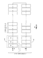
- FIG. 8 presents a diagram illustrating an exemplary solar panel configuration, in accordance with an embodiment of the present invention.
- a solar panel 800 include 72 solar cells arranged into six rows, such as a top row 802 and a second row 804 , with each row including 12 cells.
- Each solar cell can be the standard 5- or 6-inch cell.
- each solar cell is marked with its anode and cathode on its edges, although in practice the anode and cathode of a solar cell are on its top and bottom side.
- solar cells in top row 802 and second row 804 are connected in series to form a U-shaped string 806 .
- the solar cells in the middle two rows are also connected in series to form a U-shaped string 808
- the solar cells in the bottom two rows are connected in series as well to form a U-shaped string 810 .
- the three U-shaped strings 806 , 808 , and 810 are then connected to each other in parallel. More specifically, the positive outputs of all three strings are coupled together to form the positive output 812 of solar panel 800 , and the negative outputs of all strings are coupled together to form the negative output 814 of solar panel 800 .
- Parallelly connecting the strings also means that the output voltage of the panel is now the same as the voltage across each string, which is a fraction of the output voltage of a solar panel with all cells connected in series.
- the output voltage of panel 800 is 1 ⁇ 3 of a solar panel that has all of its 72 cells connected in series.
- each string is determined by the voltage across each solar cell (which is often slightly less than V oc ) and the number of serially connected cells in the string.
- V oc the voltage across each solar cell
- the output voltage of each string is increased multiple times.
- FIG. 9 presents a diagram illustrating a solar cell string with each solar cell being divided into multiple smaller cells, in accordance with an embodiment of the present invention.
- a solar cell string 900 includes a number of smaller cells.
- a conventional solar cell (such as the one represented by dotted line 902 ) is replaced by a number of serially connected smaller cells, such as cells 906 , 908 , and 910 .
- the conventional solar cell is a 6-inch square cell
- each smaller cell can have a dimension of 2-inch by 6-inch, and a conventional 6-inch square cell is replaced by three 2-inch by 6-inch smaller cells connected in series.
- the smaller cell will have the same V oc as that of the undivided solar cell.
- the current generated by each smaller cell is only a fraction of that of the original undivided cell due to its reduced size.
- the output current by solar cell string 900 is a fraction of the output current by a conventional solar cell string with undivided cells.
- the output voltage of the solar cell strings is now three times that of a solar string with undivided cells, thus making it possible to have parallelly connected strings without sacrificing the output voltage.
- V oc open circuit voltage across a standard 6-inch solar cell
- V oc _ cell open circuit voltage across a standard 6-inch solar cell
- V oc of each string is m ⁇ n ⁇ V oc _ cell
- m is the number of smaller cells as the result of dividing a conventional square shaped cell
- n is the number of conventional cells included in each string.
- I sc short circuit current
- V oc _ panel m ⁇ n ⁇ V oc _ cell
- I sc _ panel I sc _ cell
- the similar voltage and current outputs make this new panel compatible with other devices, such as inverters, that are used by a conventional solar panel with all its undivided cells connected in series. Although having similar current and voltage output, the new solar panel can extract more output power to external load because of the reduced total internal resistance.
- FIG. 10 presents a diagram illustrating an exemplary solar panel, in accordance with an embodiment of the present invention.
- solar panel 1000 includes arrays of solar cells that are arranged in a repeated pattern, such as a matrix that includes a plurality of rows.
- solar panel 1000 includes six rows of inter-connected smaller cells, with each row including 36 smaller cells. Note that each smaller cell is approximately 1 ⁇ 3 of a 6-inch standardized solar cell.
- smaller cells 1004 , 1006 , and 1008 are evenly divided portions of a standard-sized cell.
- Solar panel 1000 is configured in such a way that every two adjacent rows of smaller cells are connected in series, forming three U-shaped strings. In FIG.
- the top two rows of smaller cells are connected in series to form a solar string 1002
- the middle two rows of smaller cells are connected in series to form a solar string 1010
- the bottom two rows of smaller cells are connected in series to form a solar string 1012 .
- solar panel 1000 includes three U-shaped strings with each string including 72 smaller cells.
- the V oc and I sc of the string are 72V oc _ cell and I sc _ cell /3, respectively; and the V oc and I sc of the panel are 72 V oc _ cell , and I sc _ cell , respectively.
- Such panel level V oc and I sc are similar to those of a conventional solar panel of the same size with all its 72 cells connected in series, making it possible to adopt the same circuit equipment developed for the conventional panels.
- the total internal resistance of panel 1000 is significantly reduced. Assume that the internal resistance of a conventional cell is R cell .
- the total internal resistance is 72 R cell .
- FIG. 11 presents a flow chart illustrating the process of fabricating a solar panel, in accordance with an embodiment of the present invention.
- conventional solar cells comprising multi-layer semiconductor structures are first fabricated using conventional wafers (operation 1102 ).
- the multi-layer semiconductor structure can include a double-sided tunneling heterojunction solar cell.
- the solar cells can have a standard size, such as the standard 5-inch or 6-inch squares. In some embodiments, the solar cells are 6 ⁇ 6 inch square-shaped cells.
- front- and back-side metal grids are deposited on the front and back surfaces of the solar cells respectively to complete the bifacial solar cell fabrication (operation 1104 ).
- depositing the front- and back-side metal grids may include electroplating of a Cu grid, which is subsequently coated with Ag or Sn.
- one or more seed metal layers such as a seed Cu or Ni layer, can be deposited onto the multi-layer structures using a physical vapor deposition (PVD) technique to improve adhesion and ohmic contact quality of the electroplated Cu layer.
- PVD physical vapor deposition
- Different types of metal grids can be formed, including, but not limited to: a metal grid with a single busbar at the center and a metal grid with a single busbar at the cell edge. Note that for the edge-busbar configuration, the busbars at the front and back surfaces of the solar cells are placed at opposite edges, respectively.
- the metal grid layout allows a conventional cell to be divided into multiple smaller cells.
- the metal grid layout allows a conventional cell to be divided into multiple smaller cells.
- the metal grid layout allows a conventional cell to be divided into multiple smaller cells.
- the malleability of the Cu grid it can be difficult to cleave a wafer across the Cu grid lines. Therefore, as illustrated in FIGS. 12A and 12B , when depositing the metal grid, blank spaces can be reserved to facilitate the subsequent cell-dividing process.
- FIG. 12A presents a diagram illustrating an exemplary metal grid pattern on the front surface of a solar cell, in accordance with an embodiment of the present invention.
- metal grid 1202 includes three sub-grids, such as sub-grid 1204 .
- each sub-grid is designed to be the front-side grid for the smaller cell.
- the three sub-grid configuration allows the solar cell to be divided into three smaller cells.
- Various types of metal grid patterns can be used for each sub-grid, such as a conventional grid pattern with double busbars, a single center busbar grid pattern, a single edge busbar grid pattern, etc.
- the sub-grids have a single edge busbar pattern.
- Each sub-grid includes an edge busbar running along the longer edge of the corresponding smaller cell and a plurality of parallel finger lines running in a direction parallel to the shorter edge of the smaller cell.
- sub-grid 1204 includes an edge busbar 1206 , and a plurality of finger lines, such as finger lines 1208 and 1210 .
- a predefined blank space (with no metal deposition) is placed between the adjacent sub-grids.
- a blank space 1212 is defined to separate sub-grid 1204 from its adjacent sub-grid.
- the width of the blank space, such as blank space 1212 can be between 0.5 mm and 2 mm. Note that there is a tradeoff between a wider space that leads to an easier scribing operation and a narrower space that leads to more effective current collection. In a further embodiment, the width of such a blank space is 1 mm.
- FIG. 12B presents a diagram illustrating an exemplary metal grid pattern on the back surface of a solar cell, in accordance with an embodiment of the present invention.
- back metal grid 1220 includes three sub-grids, such as a sub-grid 1222 .
- the backside sub-grid needs to correspond to the frontside sub-grid.
- the frontside sub-grid has a single edge busbar grid pattern.
- the corresponding backside sub-grid, such as sub-grid 1222 also has an edge busbar pattern.
- the front and backside sub-grids have similar patterns except that the front and back edge busbars are located adjacent to opposite edges of the smaller cell.
- the front edge busbar is located at one edge of the front surface of the smaller cell
- the back edge busbar is located at the opposite edge of the back surface of the smaller cell.
- the locations of the blank spaces in back metal grid 1220 correspond to locations of the blank spaces in front metal grid 1202 , such that the Cu grid lines do not interfere with the subsequent wafer-cutting process.
- each solar cell is divided into multiple smaller cells (operation 1106 ).
- Various techniques can be used to divide the cells.
- a laser-based scribe-and-cleave technique is used. More specifically, a high-power laser beam is used to scribe the surface of the solar cell at the desired locations (such as blank space 1212 ) to a pre-determined depth (such as 20% of the total stack thickness), followed by applying appropriate force to cleave the scribed solar cell into multiple smaller cells.
- a pre-determined depth such as 20% of the total stack thickness
- a number of smaller cells are connected together in series to form a solar cell string (operation 1108 ).
- two rows of smaller cells with each row including 32 smaller cells are connected in series to form a U-shaped string.
- the conventional stringing process may need to be modified.
- each solar cell needs to be rotated 90 degrees, and a single tab that is as long as the long edge of the smaller cell and is between 3 and 12 mm in width can be used to connect two adjacent smaller cells.
- the width of the single tab can be between 3 and 5 mm.
- FIG. 13A presents a diagram illustrating the serial connection between two adjacent smaller cells with a single edge busbar per surface, in accordance with an embodiment of the present invention.
- smaller cell 1302 and smaller cell 1304 are coupled to each other via an edge busbar 1306 located at the top surface of smaller cell 1302 and an edge busbar 1308 located the bottom surface of smaller cell 1304 . More specifically, the bottom surface of smaller cell 1304 partially overlaps with the top surface of smaller cell 1302 at the edge in such a way that bottom edge busbar 1308 is placed on top of and in direct contact with top edge busbar 1306 .
- the edge busbars that are in contact with each other are soldered together to enable the serial electrical connection between adjacent smaller cells.
- the soldering may happen concurrently with a lamination process, during which the edge-overlapped smaller cells are placed in between a front-side cover and a back-side cover along with appropriate sealant material, which can include adhesive polymer, such as ethylene vinyl acetate (EVA).
- EVA adhesive polymer
- heat and pressure are applied to cure the sealant, sealing the solar cells between the front-side and back-side covers.
- the same heat and pressure can result in the edge busbars that are in contact, such as edge busbars 1306 and 1308 , being soldered together.
- edge busbars include a top Sn layer, there is no need to insert additional soldering or adhesive materials between the top and bottom edge busbars (such as edge busbars 1306 and 1308 ) of adjacent solar cells. Also note that because the smaller cells are relatively flexible, the pressure used during the lamination process can be relatively large without the worry that the cells may crack under such pressure. In some embodiments, the pressure applied during the lamination process can be above 1.0 atmospheres, such as 1.2 atmospheres.
- FIG. 13B presents a diagram illustrating the side-view of a string of adjacent edge-overlapped smaller cells, in accordance with an embodiment of the present invention.
- a smaller cell 1312 partially overlaps adjacent smaller cell 1314 , which also partially overlaps (on its opposite end) smaller cell 1316 .
- Such a string of smaller cells forms a pattern that is similar to roof shingles.
- the three smaller cells shown in FIG. 13B are in fact parts of a standard 6-inch square solar cell, with each smaller cell having a dimension of 2 inches by 6 inches. Compared with an undivided 6-inch solar cell, the partially overlapped smaller cells provide roughly the same photo-generation area but can lead to less power being consumed by the series resistance due to the reduced current.
- the overlapping should be kept to a minimum to minimize shading caused by the overlapping.
- the single busbars both at the top and the bottom surface
- the same shingle pattern can extend along all smaller cells in a row. To ensure that smaller cells in two adjacent rows are connected in series, the two adjacent rows need to have opposite shingle patterns, such as right-side on top for one row and left-side on top for the adjacent row.
- an extra wide metal tab can be used to serially connect the end smaller cells at the two adjacent rows. Detailed descriptions of serially connecting solar cells in a shingled pattern can be found in U.S.
- adjacent solar cells being physically coupled with direct contact in a “shingling” configuration
- the adjacent solar cells can also be coupled electrically in series using conductive materials without being in direct contact with one another.
- FIG. 13C presents a diagram illustrating the top view of an exemplary solar cell string that includes two rows of smaller cells, in accordance with an embodiment of the present invention.
- a string 1340 includes two rows of smaller cells, a top row 1342 and a bottom row 1344 .
- Each row includes a plurality of smaller cells arranged in a shingled pattern.
- the serial connection is made by the overlapped edge busbars. As a result, when viewing from the top, no busbar can be seen on each smaller cell. Therefore, this configuration can also be referred to as the “no-busbar” configuration.
- FIG. 13C presents a diagram illustrating the top view of an exemplary solar cell string that includes two rows of smaller cells, in accordance with an embodiment of the present invention.
- a string 1340 includes two rows of smaller cells, a top row 1342 and a bottom row 1344 .
- Each row includes a plurality of smaller cells arranged in a shingled pattern.
- the serial connection is made by the overlapped edge bus
- an extra wide metal tab 1346 couples together the top edge busbar of the end smaller cell of row 1342 to the bottom edge busbar of the end smaller cell of row 1344 .
- lead wires can be soldered onto the top and bottom edge busbars of the end smaller cells, forming the output electrode of string 1340 to enable electrical connections between string 1340 and other strings.
- the multiple solar strings are laid out next to each other to form a panel (operation 1110 ).
- three U-shaped strings are laid out next to each other to form a panel that includes 6 rows of smaller cells.
- the front-side cover is applied (operation 1112 ).
- the front-side cover is made of glass.
- the MPPT IC chips and bypass diode can be placed at appropriate locations, including, but not limited to: corner spacing between solar cells, and locations between adjacent solar cells (operation 1114 ).
- the MPPT IC chips and bypass diode may be implemented at a multi-cell level or string level.
- each row of smaller cells may be coupled to an MPPT IC and/or a bypass diode.
- the U-shaped strings are then connected to each other via a modified tabbing process (operation 1116 ). More specifically, the strings are connected to each other in parallel with their positive electrodes coupled together to form the positive output of the panel and negative electrodes coupled together to form the negative output of the panel. Electrical connections between the MPPT IC chips and bypass diodes and the corresponding smaller cell electrodes are formed to achieve a completely interconnected solar panel (operation 1118 ). Subsequently, the back-side cover is applied (operation 1120 ), and the entire solar panel can go through the normal lamination process, which would seal the cells, the MPPT ICs, and the bypass diode in place (operation 1122 ). Note that to ensure superior bifacial performance, the backside cover is also made of glass. The lamination process is then followed by framing and trimming (operation 1124 ), and the attachment of a junction box (operation 1126 ).
Landscapes
- Life Sciences & Earth Sciences (AREA)
- Engineering & Computer Science (AREA)
- Sustainable Energy (AREA)
- Sustainable Development (AREA)
- Photovoltaic Devices (AREA)
Abstract
Description
Claims (9)
Priority Applications (5)
| Application Number | Priority Date | Filing Date | Title |
|---|---|---|---|
| US14/563,867 US10074755B2 (en) | 2013-01-11 | 2014-12-08 | High efficiency solar panel |
| CN201580003511.1A CN105917472B (en) | 2014-01-13 | 2015-01-09 | High Efficiency Solar Panel |
| EP15701288.1A EP3095139B1 (en) | 2014-01-13 | 2015-01-09 | High efficiency solar panel |
| PCT/US2015/010916 WO2015106170A2 (en) | 2014-01-13 | 2015-01-09 | High efficiency solar panel |
| CN201520023788.8U CN204538036U (en) | 2014-01-13 | 2015-01-13 | Solar panel, solar cell, solar cell panel assembly and solar battery apparatus |
Applications Claiming Priority (5)
| Application Number | Priority Date | Filing Date | Title |
|---|---|---|---|
| US201361751733P | 2013-01-11 | 2013-01-11 | |
| US14/153,608 US9219174B2 (en) | 2013-01-11 | 2014-01-13 | Module fabrication of solar cells with low resistivity electrodes |
| US14/510,008 US9412884B2 (en) | 2013-01-11 | 2014-10-08 | Module fabrication of solar cells with low resistivity electrodes |
| US201462075134P | 2014-11-04 | 2014-11-04 | |
| US14/563,867 US10074755B2 (en) | 2013-01-11 | 2014-12-08 | High efficiency solar panel |
Related Parent Applications (1)
| Application Number | Title | Priority Date | Filing Date |
|---|---|---|---|
| US14/510,008 Continuation-In-Part US9412884B2 (en) | 2013-01-11 | 2014-10-08 | Module fabrication of solar cells with low resistivity electrodes |
Publications (2)
| Publication Number | Publication Date |
|---|---|
| US20150090314A1 US20150090314A1 (en) | 2015-04-02 |
| US10074755B2 true US10074755B2 (en) | 2018-09-11 |
Family
ID=52738902
Family Applications (1)
| Application Number | Title | Priority Date | Filing Date |
|---|---|---|---|
| US14/563,867 Active 2035-05-06 US10074755B2 (en) | 2013-01-11 | 2014-12-08 | High efficiency solar panel |
Country Status (1)
| Country | Link |
|---|---|
| US (1) | US10074755B2 (en) |
Families Citing this family (59)
| Publication number | Priority date | Publication date | Assignee | Title |
|---|---|---|---|---|
| US9012766B2 (en) | 2009-11-12 | 2015-04-21 | Silevo, Inc. | Aluminum grid as backside conductor on epitaxial silicon thin film solar cells |
| US9214576B2 (en) | 2010-06-09 | 2015-12-15 | Solarcity Corporation | Transparent conducting oxide for photovoltaic devices |
| US9773928B2 (en) | 2010-09-10 | 2017-09-26 | Tesla, Inc. | Solar cell with electroplated metal grid |
| US9800053B2 (en) | 2010-10-08 | 2017-10-24 | Tesla, Inc. | Solar panels with integrated cell-level MPPT devices |
| US9054256B2 (en) | 2011-06-02 | 2015-06-09 | Solarcity Corporation | Tunneling-junction solar cell with copper grid for concentrated photovoltaic application |
| US9865754B2 (en) | 2012-10-10 | 2018-01-09 | Tesla, Inc. | Hole collectors for silicon photovoltaic cells |
| US9219174B2 (en) | 2013-01-11 | 2015-12-22 | Solarcity Corporation | Module fabrication of solar cells with low resistivity electrodes |
| US10074755B2 (en) | 2013-01-11 | 2018-09-11 | Tesla, Inc. | High efficiency solar panel |
| US9412884B2 (en) | 2013-01-11 | 2016-08-09 | Solarcity Corporation | Module fabrication of solar cells with low resistivity electrodes |
| US10309012B2 (en) | 2014-07-03 | 2019-06-04 | Tesla, Inc. | Wafer carrier for reducing contamination from carbon particles and outgassing |
| US9590132B2 (en) | 2014-12-05 | 2017-03-07 | Solarcity Corporation | Systems and methods for cascading photovoltaic structures |
| US10043937B2 (en) | 2014-12-05 | 2018-08-07 | Solarcity Corporation | Systems and method for precision automated placement of backsheet on PV modules |
| US9899546B2 (en) * | 2014-12-05 | 2018-02-20 | Tesla, Inc. | Photovoltaic cells with electrodes adapted to house conductive paste |
| US9685579B2 (en) | 2014-12-05 | 2017-06-20 | Solarcity Corporation | Photovoltaic structure cleaving system |
| US9991412B2 (en) | 2014-12-05 | 2018-06-05 | Solarcity Corporation | Systems for precision application of conductive adhesive paste on photovoltaic structures |
| US10236406B2 (en) | 2014-12-05 | 2019-03-19 | Solarcity Corporation | Systems and methods for targeted annealing of photovoltaic structures |
| US10056522B2 (en) | 2014-12-05 | 2018-08-21 | Solarcity Corporation | System and apparatus for precision automation of tab attachment for fabrications of solar panels |
| US9947822B2 (en) | 2015-02-02 | 2018-04-17 | Tesla, Inc. | Bifacial photovoltaic module using heterojunction solar cells |
| CN105047731B (en) * | 2015-07-02 | 2017-12-22 | 苏州阿特斯阳光电力科技有限公司 | A kind of back contact solar cell component |
| US9761744B2 (en) | 2015-10-22 | 2017-09-12 | Tesla, Inc. | System and method for manufacturing photovoltaic structures with a metal seed layer |
| US20170179324A1 (en) * | 2015-12-14 | 2017-06-22 | Solarcity Corporation | High-efficiency low-cost solar panel with protection circuitry |
| US9966487B2 (en) * | 2015-12-14 | 2018-05-08 | Solarcity Corporation | Strain relief apparatus for solar modules |
| US9842956B2 (en) | 2015-12-21 | 2017-12-12 | Tesla, Inc. | System and method for mass-production of high-efficiency photovoltaic structures |
| US10115838B2 (en) * | 2016-04-19 | 2018-10-30 | Tesla, Inc. | Photovoltaic structures with interlocking busbars |
| JP2019515483A (en) * | 2016-05-06 | 2019-06-06 | アプライド マテリアルズ イタリア エス. アール. エル. | Apparatus for manufacturing at least two solar cell configurations, system for manufacturing at least two tiled solar cells, and method for manufacturing at least two solar cell configurations |
| US10868211B2 (en) | 2016-05-06 | 2020-12-15 | Applied Materials Italia S.R.L. | Apparatus for manufacture of at least two solar cell arrangements, system for manufacture of at least two shingled solar cells, and method for manufacture of at least two solar cell arrangements |
| FR3054726B1 (en) * | 2016-07-29 | 2019-05-17 | Commissariat A L'energie Atomique Et Aux Energies Alternatives | METHOD FOR MANUFACTURING A PHOTOVOLTAIC ELEMENT |
| US9960302B1 (en) * | 2016-10-18 | 2018-05-01 | Tesla, Inc. | Cascaded photovoltaic structures with interdigitated back contacts |
| US10937915B2 (en) | 2016-10-28 | 2021-03-02 | Tesla, Inc. | Obscuring, color matching, and camouflaging solar panels |
| US12598838B2 (en) | 2016-11-09 | 2026-04-07 | Tesla, Inc. | System and methods for achieving a micro louver effect in a photovoltaic cell |
| US11502213B2 (en) | 2016-12-30 | 2022-11-15 | Sunpower Corporation | Solar cell having a plurality of sub-cells coupled by cell level interconnection |
| AU2018410566B2 (en) | 2017-03-01 | 2021-02-18 | Tesla, Inc. | System and method for packaging photovoltaic roof tiles |
| CN110277458A (en) * | 2017-03-09 | 2019-09-24 | 伟创力有限公司 | Shingled array solar cells and methods of making solar modules including shingled array solar cells |
| USD841570S1 (en) | 2017-08-25 | 2019-02-26 | Flex Ltd | Solar cell |
| USD841571S1 (en) | 2017-08-25 | 2019-02-26 | Flex Ltd. | Solar panel |
| US10381973B2 (en) | 2017-05-17 | 2019-08-13 | Tesla, Inc. | Uniformly and directionally colored photovoltaic modules |
| US11258398B2 (en) | 2017-06-05 | 2022-02-22 | Tesla, Inc. | Multi-region solar roofing modules |
| US10734938B2 (en) | 2017-07-21 | 2020-08-04 | Tesla, Inc. | Packaging for solar roof tiles |
| TWI661572B (en) * | 2017-07-21 | 2019-06-01 | 海力雅集成股份有限公司 | Solar module and the manufacture thereof |
| US10857764B2 (en) | 2017-07-25 | 2020-12-08 | Tesla, Inc. | Method for improving adhesion between glass cover and encapsulant for solar roof tiles |
| US10672919B2 (en) | 2017-09-19 | 2020-06-02 | Tesla, Inc. | Moisture-resistant solar cells for solar roof tiles |
| US10978990B2 (en) | 2017-09-28 | 2021-04-13 | Tesla, Inc. | Glass cover with optical-filtering coating for managing color of a solar roof tile |
| US10454409B2 (en) | 2018-02-02 | 2019-10-22 | Tesla, Inc. | Non-flat solar roof tiles |
| US10862420B2 (en) | 2018-02-20 | 2020-12-08 | Tesla, Inc. | Inter-tile support for solar roof tiles |
| US11190128B2 (en) | 2018-02-27 | 2021-11-30 | Tesla, Inc. | Parallel-connected solar roof tile modules |
| US11431279B2 (en) | 2018-07-02 | 2022-08-30 | Tesla, Inc. | Solar roof tile with a uniform appearance |
| US11082005B2 (en) | 2018-07-31 | 2021-08-03 | Tesla, Inc. | External electrical contact for solar roof tiles |
| US11245354B2 (en) | 2018-07-31 | 2022-02-08 | Tesla, Inc. | Solar roof tile spacer with embedded circuitry |
| US11245355B2 (en) | 2018-09-04 | 2022-02-08 | Tesla, Inc. | Solar roof tile module |
| US11581843B2 (en) | 2018-09-14 | 2023-02-14 | Tesla, Inc. | Solar roof tile free of back encapsulant layer |
| CN109065656A (en) * | 2018-10-31 | 2018-12-21 | 伟创力有限公司 | The method for forming the colored electro-conductive welding for being integrated in solar cell module |
| CN110165006B (en) * | 2019-06-17 | 2020-10-20 | 苏州亚傲鑫企业管理咨询有限公司 | A Polarity Complementary Crystalline Silicon Photovoltaic Cell Connection Group |
| US12033811B2 (en) * | 2019-07-02 | 2024-07-09 | Novaled Gmbh | Solar cell |
| US11431280B2 (en) | 2019-08-06 | 2022-08-30 | Tesla, Inc. | System and method for improving color appearance of solar roofs |
| US11456695B2 (en) | 2020-01-20 | 2022-09-27 | Erthos, Inc. | Leading edge units device and methods |
| US20210091709A1 (en) * | 2019-09-20 | 2021-03-25 | Erthos Inc. | Flat Tile Solar Panels |
| US12074560B2 (en) | 2020-01-20 | 2024-08-27 | Erthos IP LLC | Edge units device and methods |
| WO2021096879A1 (en) * | 2019-11-12 | 2021-05-20 | Solaria Corporation | Bifacial photovoltaic module |
| US11764315B2 (en) * | 2020-09-16 | 2023-09-19 | Maxeon Solar Pte. Ltd. | Solar cell separation with edge coating |
Citations (451)
| Publication number | Priority date | Publication date | Assignee | Title |
|---|---|---|---|---|
| US819360A (en) | 1905-03-22 | 1906-05-01 | Edward Newton A | Electrical switch. |
| US2626907A (en) | 1951-05-14 | 1953-01-27 | Petrolite Corp | Process for breaking petroleum emulsions |
| US2938938A (en) | 1956-07-03 | 1960-05-31 | Hoffman Electronics Corp | Photo-voltaic semiconductor apparatus or the like |
| US3094439A (en) | 1961-07-24 | 1963-06-18 | Spectrolab | Solar cell system |
| US3116171A (en) | 1961-03-14 | 1963-12-31 | Bell Telephone Labor Inc | Satellite solar cell assembly |
| US3459597A (en) | 1966-02-04 | 1969-08-05 | Trw Inc | Solar cells with flexible overlapping bifurcated connector |
| US3676179A (en) | 1968-10-03 | 1972-07-11 | Gulf Oil Corp | Coated article and method for making same |
| US3961997A (en) | 1975-05-12 | 1976-06-08 | The United States Of America As Represented By The Administrator Of The National Aeronautics And Space Administration | Fabrication of polycrystalline solar cells on low-cost substrates |
| US3969163A (en) | 1974-09-19 | 1976-07-13 | Texas Instruments Incorporated | Vapor deposition method of forming low cost semiconductor solar cells including reconstitution of the reacted gases |
| US4015280A (en) | 1974-10-19 | 1977-03-29 | Sony Corporation | Multi-layer semiconductor photovoltaic device |
| US4082568A (en) | 1977-05-10 | 1978-04-04 | Joseph Lindmayer | Solar cell with multiple-metal contacts |
| US4124410A (en) | 1977-11-21 | 1978-11-07 | Union Carbide Corporation | Silicon solar cells with low-cost substrates |
| US4193975A (en) | 1977-11-21 | 1980-03-18 | Union Carbide Corporation | Process for the production of improved refined metallurgical silicon |
| US4200621A (en) | 1978-07-18 | 1980-04-29 | Motorola, Inc. | Sequential purification and crystal growth |
| US4213798A (en) | 1979-04-27 | 1980-07-22 | Rca Corporation | Tellurium schottky barrier contact for amorphous silicon solar cells |
| US4251285A (en) | 1979-08-14 | 1981-02-17 | Westinghouse Electric Corp. | Diffusion of dopant from optical coating and single step formation of PN junction in silicon solar cell and coating thereon |
| US4284490A (en) | 1978-09-28 | 1981-08-18 | Coulter Systems Corporation | R.F. Sputtering apparatus including multi-network power supply |
| US4315096A (en) | 1980-07-25 | 1982-02-09 | Eastman Kodak Company | Integrated array of photovoltaic cells having minimized shorting losses |
| US4336648A (en) | 1979-11-02 | 1982-06-29 | Licentia Patent-Verwaltungs-G.M.B.H. | Method of contacting a solar cell |
| US4342044A (en) | 1978-03-08 | 1982-07-27 | Energy Conversion Devices, Inc. | Method for optimizing photoresponsive amorphous alloys and devices |
| US4431858A (en) | 1982-05-12 | 1984-02-14 | University Of Florida | Method of making quasi-grain boundary-free polycrystalline solar cell structure and solar cell structure obtained thereby |
| US4514579A (en) | 1984-01-30 | 1985-04-30 | Energy Conversion Devices, Inc. | Large area photovoltaic cell and method for producing same |
| US4540843A (en) | 1983-03-09 | 1985-09-10 | Licentia Patent-Verwaltungs-Gmbh | Solar cell |
| US4567642A (en) | 1984-09-28 | 1986-02-04 | The Standard Oil Company | Method of making photovoltaic modules |
| US4571448A (en) | 1981-11-16 | 1986-02-18 | University Of Delaware | Thin film photovoltaic solar cell and method of making the same |
| US4577051A (en) | 1984-09-28 | 1986-03-18 | The Standard Oil Company | Bypass diode assembly for photovoltaic modules |
| US4586988A (en) | 1983-08-19 | 1986-05-06 | Energy Conversion Devices, Inc. | Method of forming an electrically conductive member |
| US4589191A (en) | 1983-10-20 | 1986-05-20 | Unisearch Limited | Manufacture of high efficiency solar cells |
| US4612409A (en) | 1981-11-04 | 1986-09-16 | Kanegafuchi Kagaku Kogyo Kabushiki Kaisha | Flexible photovoltaic device |
| US4617421A (en) | 1985-04-01 | 1986-10-14 | Sovonics Solar Systems | Photovoltaic cell having increased active area and method for producing same |
| US4633033A (en) | 1985-02-08 | 1986-12-30 | Energy Conversion Devices, Inc. | Photovoltaic device and method |
| US4652693A (en) | 1985-08-30 | 1987-03-24 | The Standard Oil Company | Reformed front contact current collector grid and cell interconnect for a photovoltaic cell module |
| US4657060A (en) | 1982-03-01 | 1987-04-14 | Graber Industries, Inc. | Vertical venetian blind with inline drive |
| US4667060A (en) | 1985-05-28 | 1987-05-19 | Spire Corporation | Back junction photovoltaic solar cell |
| US4694115A (en) | 1986-11-04 | 1987-09-15 | Spectrolab, Inc. | Solar cell having improved front surface metallization |
| US4729970A (en) | 1986-09-15 | 1988-03-08 | Energy Conversion Devices, Inc. | Conversion process for passivating short circuit current paths in semiconductor devices |
| US4753683A (en) | 1985-09-09 | 1988-06-28 | Hughes Aircraft Company | Gallium arsenide solar cell system |
| US4771017A (en) | 1987-06-23 | 1988-09-13 | Spire Corporation | Patterning process |
| US4784702A (en) | 1986-04-22 | 1988-11-15 | Thomson-Csf | PIN photodiode formed from an amorphous semiconductor |
| US4877460A (en) | 1987-03-17 | 1989-10-31 | Telefunken Electronic Gmbh | Solar cell module |
| US4933061A (en) | 1988-12-29 | 1990-06-12 | Trifari, Krussman & Fishel, Inc. | Electroplating tank |
| US4968384A (en) | 1988-09-29 | 1990-11-06 | Fuji Electric Corporate Research And Development Ltd. | Method of producing carbon-doped amorphous silicon thin film |
| US5053355A (en) | 1989-01-14 | 1991-10-01 | Nukem Gmbh | Method and means for producing a layered system of semiconductors |
| US5057163A (en) | 1988-05-04 | 1991-10-15 | Astropower, Inc. | Deposited-silicon film solar cell |
| WO1991017839A1 (en) | 1990-05-18 | 1991-11-28 | Bp Chemicals (Hitco) Inc. | Materials for chemical vapor deposition processes |
| US5075763A (en) | 1988-09-28 | 1991-12-24 | Kopin Corporation | High temperature metallization system for contacting semiconductor materials |
| WO1991020097A1 (en) | 1990-05-14 | 1991-12-26 | The Boeing Company | Tandem photovoltaic solar cell with iii-v diffused junction booster cell |
| US5084107A (en) | 1989-06-05 | 1992-01-28 | Mitsubishi Denki Kabushiki Kaisha | Solar cell and solar cell array with adhered electrode |
| DE4030713A1 (en) | 1990-09-28 | 1992-04-02 | Telefunken Systemtechnik | Photoelectric solar generator - has flexible intermediate connecting plate designed to prevent solar cell fracture due to temp. change stresses |
| US5118361A (en) | 1990-05-21 | 1992-06-02 | The Boeing Company | Terrestrial concentrator solar cell module |
| US5131933A (en) | 1990-03-23 | 1992-07-21 | Telefunken Systemtechnik Gmbh | Solar cell |
| JPH04245683A (en) | 1991-01-31 | 1992-09-02 | Tonen Corp | Manufacture of solar cell |
| US5155051A (en) | 1990-06-22 | 1992-10-13 | Sanyo Electric Co., Ltd. | Method of manufacturing photovoltaic device |
| US5178685A (en) | 1991-06-11 | 1993-01-12 | Mobil Solar Energy Corporation | Method for forming solar cell contacts and interconnecting solar cells |
| US5181968A (en) | 1991-06-24 | 1993-01-26 | United Solar Systems Corporation | Photovoltaic device having an improved collector grid |
| US5213628A (en) | 1990-09-20 | 1993-05-25 | Sanyo Electric Co., Ltd. | Photovoltaic device |
| US5217539A (en) | 1991-09-05 | 1993-06-08 | The Boeing Company | III-V solar cells and doping processes |
| US5279682A (en) | 1991-06-11 | 1994-01-18 | Mobil Solar Energy Corporation | Solar cell and method of making same |
| US5286306A (en) | 1992-02-07 | 1994-02-15 | Shalini Menezes | Thin film photovoltaic cells from I-III-VI-VII compounds |
| JPH06196766A (en) | 1992-12-24 | 1994-07-15 | Fujitsu Ltd | Superconducting transistor |
| US5364518A (en) | 1991-05-28 | 1994-11-15 | Leybold Aktiengesellschaft | Magnetron cathode for a rotating target |
| US5401331A (en) | 1993-09-07 | 1995-03-28 | Midwest Research Institute | Substrate for thin silicon solar cells |
| JPH07249788A (en) | 1994-03-11 | 1995-09-26 | Tonen Corp | Solar cell |
| US5455430A (en) | 1991-08-01 | 1995-10-03 | Sanyo Electric Co., Ltd. | Photovoltaic device having a semiconductor grade silicon layer formed on a metallurgical grade substrate |
| US5461002A (en) | 1990-05-30 | 1995-10-24 | Safir; Yakov | Method of making diffused doped areas for semiconductor components |
| US5563092A (en) | 1993-04-23 | 1996-10-08 | Canon Kabushiki Kaisha | Method of producing a substrate for an amorphous semiconductor |
| US5576241A (en) | 1994-05-31 | 1996-11-19 | Fuji Electric Co., Ltd. | Method of separating semiconductor wafer with dielectrics |
| US5627081A (en) | 1994-11-29 | 1997-05-06 | Midwest Research Institute | Method for processing silicon solar cells |
| US5676766A (en) | 1993-09-30 | 1997-10-14 | Siemens Aktiengesellschaft | Solar cell having a chalcopyrite absorber layer |
| US5681402A (en) | 1994-11-04 | 1997-10-28 | Canon Kabushiki Kaisha | Photovoltaic element |
| US5698451A (en) | 1988-06-10 | 1997-12-16 | Mobil Solar Energy Corporation | Method of fabricating contacts for solar cells |
| JPH104204A (en) | 1996-06-18 | 1998-01-06 | Sharp Corp | Solar cell manufacturing method |
| US5705828A (en) | 1991-08-10 | 1998-01-06 | Sanyo Electric Co., Ltd. | Photovoltaic device |
| US5726065A (en) | 1995-02-21 | 1998-03-10 | Imec Vzw | Method of preparing solar cell front contacts |
| US5808315A (en) | 1992-07-21 | 1998-09-15 | Semiconductor Energy Laboratory Co., Ltd. | Thin film transistor having transparent conductive film |
| US5814195A (en) | 1995-04-25 | 1998-09-29 | The Boc Group, Inc. | Sputtering system using cylindrical rotating magnetron electrically powered using alternating current |
| JPH1131834A (en) | 1997-07-10 | 1999-02-02 | Showa Shell Sekiyu Kk | Glass sandwich solar panel |
| US5903382A (en) | 1997-12-19 | 1999-05-11 | Rockwell International Corporation | Electrodeposition cell with high light transmission |
| US5935345A (en) | 1994-07-13 | 1999-08-10 | Centre National De La Recherche Scientifique, Etablissement Public A Caractere Scientifique Et Technologique | Process for the production of a photovoltaic material or device, material or device thus obtained, and photocell comprising such a material or device |
| US6017581A (en) | 1997-04-18 | 2000-01-25 | Semi-Alloys Company | Method for coating lenticular articles |
| US6034322A (en) | 1999-07-01 | 2000-03-07 | Space Systems/Loral, Inc. | Solar cell assembly |
| JP2000164902A (en) | 1998-11-27 | 2000-06-16 | Kyocera Corp | Solar cell |
| US6091019A (en) | 1997-09-26 | 2000-07-18 | Sanyo Electric Co., Ltd. | Photovoltaic element and manufacturing method thereof |
| US6140570A (en) | 1997-10-29 | 2000-10-31 | Canon Kabushiki Kaisha | Photovoltaic element having a back side transparent and electrically conductive layer with a light incident side surface region having a specific cross section and a module comprising said photovolatic element |
| US6232545B1 (en) | 1998-08-06 | 2001-05-15 | Jx Crystals Inc. | Linear circuit designs for solar photovoltaic concentrator and thermophotovoltaic applications using cell and substrate materials with matched coefficients of thermal expansion |
| US20010008143A1 (en) | 1998-05-20 | 2001-07-19 | Makoto Sasaoka | Photovoltaic power generating structure |
| US6303853B1 (en) | 1998-08-06 | 2001-10-16 | Jx Crystals Inc. | Shingle circuits for thermophotovoltaic systems |
| US6333457B1 (en) | 2000-08-29 | 2001-12-25 | Sunpower Corporation | Edge passivated silicon solar/photo cell and method of manufacture |
| US20020015881A1 (en) | 2000-06-13 | 2002-02-07 | Yoshisada Nakamura | Photoelectric conversion device and photo cell |
| JP2002057357A (en) | 2000-08-11 | 2002-02-22 | Fuji Electric Co Ltd | Thin film solar cell and method of manufacturing the same |
| US20020072207A1 (en) | 2000-12-12 | 2002-06-13 | Hideyuki Andoh | Semiconductor device and manufacturing method thereof |
| US6410843B1 (en) | 1999-11-22 | 2002-06-25 | Sanyo Electric Co., Ltd. | Solar cell module |
| US20020086456A1 (en) | 2000-12-19 | 2002-07-04 | Cunningham Shawn Jay | Bulk micromachining process for fabricating an optical MEMS device with integrated optical aperture |
| US6441297B1 (en) | 1998-03-13 | 2002-08-27 | Steffen Keller | Solar cell arrangement |
| US6468828B1 (en) | 1998-07-14 | 2002-10-22 | Sky Solar L.L.C. | Method of manufacturing lightweight, high efficiency photovoltaic module |
| US20020176404A1 (en) | 2001-04-13 | 2002-11-28 | Girard Gregory D. | Distributed edge switching system for voice-over-packet multiservice network |
| US6488824B1 (en) | 1998-11-06 | 2002-12-03 | Raycom Technologies, Inc. | Sputtering apparatus and process for high rate coatings |
| US20020189939A1 (en) | 2001-06-14 | 2002-12-19 | German John R. | Alternating current rotatable sputter cathode |
| US20030000568A1 (en) | 2001-06-15 | 2003-01-02 | Ase Americas, Inc. | Encapsulated photovoltaic modules and method of manufacturing same |
| US20030000571A1 (en) | 2001-06-13 | 2003-01-02 | Junzou Wakuda | Solar cell and method of producing the same |
| US20030034062A1 (en) | 2001-08-17 | 2003-02-20 | Stern Theodore Garry | Electrostatically clean solar array |
| US20030042516A1 (en) | 2001-08-30 | 2003-03-06 | Micron Technology, Inc. | Technique to control tunneling currents in dram capacitors, cells, and devices |
| US6538193B1 (en) | 2000-04-21 | 2003-03-25 | Jx Crystals Inc. | Thermophotovoltaic generator in high temperature industrial process |
| US20030070705A1 (en) | 2001-10-11 | 2003-04-17 | Hayden Herbert T. | Structure for supporting a photovoltaic module in a solar energy collection system |
| US6552414B1 (en) | 1996-12-24 | 2003-04-22 | Imec Vzw | Semiconductor device with selectively diffused regions |
| US20030097447A1 (en) | 2001-10-25 | 2003-05-22 | Johnston Alan B. | Bridging user agent and a proxy server for supporting network services |
| US20030116185A1 (en) | 2001-11-05 | 2003-06-26 | Oswald Robert S. | Sealed thin film photovoltaic modules |
| US20030118865A1 (en) | 2001-08-27 | 2003-06-26 | Marks Tobin J. | High work function transparent conducting oxides as anodes for organic light-emitting diodes |
| US6586270B2 (en) | 2000-06-01 | 2003-07-01 | Canon Kabushiki Kaisha | Process for producing a photovoltaic element |
| US20030121228A1 (en) | 2001-12-31 | 2003-07-03 | Stoehr Robert P. | System and method for dendritic web solar cell shingling |
| US20030136440A1 (en) | 2000-03-13 | 2003-07-24 | Akio Machida | Optical energy transducer |
| US20030168578A1 (en) | 2001-11-29 | 2003-09-11 | Mikio Taguchi | Photovoltaic device and manufacturing method thereof |
| US6620645B2 (en) | 2000-11-16 | 2003-09-16 | G.T. Equipment Technologies, Inc | Making and connecting bus bars on solar cells |
| US20030183270A1 (en) | 2000-08-31 | 2003-10-02 | Fritz Falk | Multicrystalline laser-crystallized silicon thin layer solar cell deposited on a glass substrate |
| WO2003083953A1 (en) | 2002-03-29 | 2003-10-09 | Ebara Corporation | Solar cell and method of manufacturing the same |
| US20030201007A1 (en) | 2002-04-24 | 2003-10-30 | Fraas Lewis M. | Planar solar concentrator power module |
| US6672018B2 (en) | 2001-10-12 | 2004-01-06 | Jefferson Shingleton | Solar module mounting method and clip |
| US6683360B1 (en) | 2002-01-24 | 2004-01-27 | Fillfactory | Multiple or graded epitaxial wafers for particle or radiation detection |
| US20040035458A1 (en) | 2002-08-20 | 2004-02-26 | Kevin Beernink | Series connected photovoltaic module and method for its manufacture |
| US20040065363A1 (en) | 2002-10-02 | 2004-04-08 | The Boeing Company | Isoelectronic surfactant induced sublattice disordering in optoelectronic devices |
| US6736948B2 (en) | 2002-01-18 | 2004-05-18 | Von Ardenne Anlagentechnik Gmbh | Cylindrical AC/DC magnetron with compliant drive system and improved electrical and thermal isolation |
| US20040103937A1 (en) | 2002-09-09 | 2004-06-03 | Interuniversitair Microelektronica Centrum (Imec) | Photovoltaic device |
| US20040112426A1 (en) | 2002-12-11 | 2004-06-17 | Sharp Kabushiki Kaisha | Solar cell and method of manufacturing the same |
| US20040112419A1 (en) * | 2001-03-21 | 2004-06-17 | Bernard Boulanger | Solar panel having electrical terminals distributed across the surface thereof |
| US20040123897A1 (en) | 2001-03-19 | 2004-07-01 | Satoyuki Ojima | Solar cell and its manufacturing method |
| US6761771B2 (en) | 2000-10-19 | 2004-07-13 | Asm Japan K.K. | Semiconductor substrate-supporting apparatus |
| US20040135979A1 (en) | 2003-01-13 | 2004-07-15 | Nikon Corporation | Vibration-attenuation devices and methods using pressurized bellows exhibiting substantially zero lateral stiffness |
| US20040152326A1 (en) | 2003-01-28 | 2004-08-05 | Kyocera Corporation | Multicrystalline silicon substrate and process for roughening surface thereof |
| US20040185683A1 (en) | 2003-03-20 | 2004-09-23 | Hiroki Nakamura | Wiring, display device and method of manufacturing the same |
| US20040200520A1 (en) | 2003-04-10 | 2004-10-14 | Sunpower Corporation | Metal contact structure for solar cell and method of manufacture |
| US6841051B2 (en) | 2002-03-14 | 2005-01-11 | Sputtering Components, Inc. | High-power ion sputtering magnetron |
| US20050009319A1 (en) | 2003-07-08 | 2005-01-13 | Kazuhide Abe | Method of forming buried wiring in semiconductor device |
| US20050012095A1 (en) | 2003-06-26 | 2005-01-20 | Kyocera Corporation | Semiconductor/electrode contact structure and semiconductor device using the same |
| US20050022861A1 (en) | 2003-08-01 | 2005-02-03 | Rose Douglas H. | Etching of solar cell materials |
| US20050022746A1 (en) | 2003-08-01 | 2005-02-03 | Sgl Carbon, Llc | Holder for supporting wafers during semiconductor manufacture |
| US20050061665A1 (en) | 2003-08-06 | 2005-03-24 | Sunpower Corporation | Substrate carrier for electroplating solar cells |
| US20050062041A1 (en) | 2003-09-24 | 2005-03-24 | Sanyo Electric Co., Ltd. | Photovoltaic cell and method of fabricating the same |
| US20050074954A1 (en) | 2002-10-11 | 2005-04-07 | Hideo Yamanaka | Method and apparatus for producing ultra-thin semiconductor chip and method and apparatus for producing ultra-thin back-illuminated solid-state image pickup device |
| US20050109388A1 (en) | 2003-11-05 | 2005-05-26 | Canon Kabushiki Kaisha | Photovoltaic device and manufacturing method thereof |
| JP2005159312A (en) | 2003-11-05 | 2005-06-16 | Canon Inc | Base material for polycrystalline silicon substrate for solar cell and polycrystalline silicon substrate for solar cell |
| US20050126622A1 (en) | 2003-12-11 | 2005-06-16 | Canon Kabushiki Kaisha | Solar cell module and method of producing the same |
| US20050133084A1 (en) | 2003-10-10 | 2005-06-23 | Toshio Joge | Silicon solar cell and production method thereof |
| US20050178662A1 (en) | 2002-03-22 | 2005-08-18 | Dieter Wurczinger | Rotating tubular cathode |
| US20050189015A1 (en) | 2003-10-30 | 2005-09-01 | Ajeet Rohatgi | Silicon solar cells and methods of fabrication |
| US20050199279A1 (en) | 2004-01-29 | 2005-09-15 | Sanyo Electric Co., Ltd. | Solar cell module |
| US20050252544A1 (en) | 2004-05-11 | 2005-11-17 | Ajeet Rohatgi | Silicon solar cells and methods of fabrication |
| US20050257823A1 (en) | 2004-05-19 | 2005-11-24 | Dutch Space B.V. | Solar cell assembly |
| US20050268963A1 (en) | 2004-02-24 | 2005-12-08 | David Jordan | Process for manufacturing photovoltaic cells |
| KR20050122721A (en) | 2004-06-25 | 2005-12-29 | 한국전기연구원 | Light sensitized and p-n junction silicon complexed solar cell and manufacturing method thereof |
| KR20060003277A (en) | 2004-07-05 | 2006-01-10 | 전자부품연구원 | Solar cell having zinc oxide thin film and manufacturing method thereof |
| US20060012000A1 (en) | 2001-05-21 | 2006-01-19 | Estes Michael J | Thin-film transistors based on tunneling structures and applications |
| US20060060791A1 (en) | 2004-09-08 | 2006-03-23 | Nikon Corporation | Bellows with spring anti-gravity device |
| US20060060238A1 (en) | 2004-02-05 | 2006-03-23 | Advent Solar, Inc. | Process and fabrication methods for emitter wrap through back contact solar cells |
| US7030413B2 (en) | 2000-09-05 | 2006-04-18 | Sanyo Electric Co., Ltd. | Photovoltaic device with intrinsic amorphous film at junction, having varied optical band gap through thickness thereof |
| US20060130891A1 (en) | 2004-10-29 | 2006-06-22 | Carlson David E | Back-contact photovoltaic cells |
| US20060154389A1 (en) | 2005-01-11 | 2006-07-13 | Doan Trung T | Light emitting diode with conducting metal substrate |
| WO2006097189A1 (en) | 2005-03-14 | 2006-09-21 | Q-Cells Ag | Solar cell |
| US20060213548A1 (en) | 2005-03-22 | 2006-09-28 | Applied Materials, Inc. | Scalable photovoltaic cell and solar panel manufacturing with improved wiring |
| US20060231803A1 (en) | 2005-04-14 | 2006-10-19 | Yueli Wang | Electroconductive thick film composition(s), electrode(s), and semiconductor device(s) formed therefrom |
| US20060255340A1 (en) | 2005-05-12 | 2006-11-16 | Venkatesan Manivannan | Surface passivated photovoltaic devices |
| US20060260673A1 (en) * | 2003-10-17 | 2006-11-23 | Canon Kabushiki Kaisha | Photovoltaic element and method of producing photovoltaic element |
| JP2006324504A (en) | 2005-05-19 | 2006-11-30 | Shin Etsu Handotai Co Ltd | Solar cell |
| US20060272698A1 (en) | 2005-06-06 | 2006-12-07 | Durvasula Ravi S | Photovoltaic concentrator for solar energy system |
| US20060283496A1 (en) | 2005-06-16 | 2006-12-21 | Sanyo Electric Co., Ltd. | Method for manufacturing photovoltaic module |
| US20060283499A1 (en) | 2005-02-25 | 2006-12-21 | Sanyo Electric Co., Ltd. | Photovoltaic cell |
| US7164150B2 (en) | 2002-03-05 | 2007-01-16 | Sanyo Electric Co., Ltd. | Photovoltaic device and manufacturing method thereof |
| US20070023081A1 (en) | 2005-07-28 | 2007-02-01 | General Electric Company | Compositionally-graded photovoltaic device and fabrication method, and related articles |
| US20070023082A1 (en) | 2005-07-28 | 2007-02-01 | Venkatesan Manivannan | Compositionally-graded back contact photovoltaic devices and methods of fabricating such devices |
| EP1770791A1 (en) | 2005-09-30 | 2007-04-04 | Sanyo Electric Co., Ltd. | Rectangular shaped solar cell module and its manufacturing method using hexagonal shaped unit solar cells |
| US20070108437A1 (en) | 1998-06-08 | 2007-05-17 | Avto Tavkhelidze | Method of fabrication of high temperature superconductors based on new mechanism of electron-electron interaction |
| US20070132034A1 (en) | 2005-12-14 | 2007-06-14 | Giuseppe Curello | Isolation body for semiconductor devices and method to form the same |
| US20070137699A1 (en) | 2005-12-16 | 2007-06-21 | General Electric Company | Solar cell and method for fabricating solar cell |
| US20070148336A1 (en) | 2005-11-07 | 2007-06-28 | Robert Bachrach | Photovoltaic contact and wiring formation |
| EP1806684A1 (en) | 2005-12-05 | 2007-07-11 | Sap Ag | Creation of structured order items during availability check |
| US20070186853A1 (en) | 2006-02-10 | 2007-08-16 | Veeco Instruments Inc. | System and method for varying wafer surface temperature via wafer-carrier temperature offset |
| US20070186968A1 (en) | 2006-01-24 | 2007-08-16 | Atsushi Nakauchi | Photovoltaic Module |
| US20070187652A1 (en) | 2005-12-21 | 2007-08-16 | Takuya Konno | Paste for solar cell electrodes, method for the manufacture of solar cell electrodes, and the solar cell |
| US20070186970A1 (en) | 2003-05-09 | 2007-08-16 | Masatoshi Takahashi | Solar cell and method of fabricating the same |
| DE102006009194A1 (en) | 2006-02-22 | 2007-08-23 | Siegfried Gutfleisch | Arrangement of a load-bearing building structure and a solar cell construction |
| US20070202029A1 (en) | 2003-12-04 | 2007-08-30 | Gary Burns | Method Of Removing Impurities From Metallurgical Grade Silicon To Produce Solar Grade Silicon |
| US20070235829A1 (en) | 2005-02-11 | 2007-10-11 | Levine Peter A | Dark Current Reduction in Back-Illuminated Imaging Sensors and Method of Fabricating Same |
| US20070235077A1 (en) | 2006-03-27 | 2007-10-11 | Kyocera Corporation | Solar Cell Module and Manufacturing Process Thereof |
| US20070256728A1 (en) | 2006-05-04 | 2007-11-08 | Sunpower Corporation | Solar cell having doped semiconductor heterojunction contacts |
| US20070274504A1 (en) | 2006-05-12 | 2007-11-29 | Oracle International Corporation | Customized sip routing to cross firewalls |
| US20070283997A1 (en) | 2006-06-13 | 2007-12-13 | Miasole | Photovoltaic module with integrated current collection and interconnection |
| US20070283996A1 (en) | 2006-06-13 | 2007-12-13 | Miasole | Photovoltaic module with insulating interconnect carrier |
| US20080000522A1 (en) | 2006-06-30 | 2008-01-03 | General Electric Company | Photovoltaic device which includes all-back-contact configuration; and related processes |
| US20080011350A1 (en) * | 1999-03-30 | 2008-01-17 | Daniel Luch | Collector grid, electrode structures and interconnect structures for photovoltaic arrays and other optoelectric devices |
| US7328534B2 (en) | 2002-02-20 | 2008-02-12 | Sunpower Corporation, Systems | Shingle system |
| US20080035489A1 (en) | 2006-06-05 | 2008-02-14 | Rohm And Haas Electronic Materials Llc | Plating process |
| US20080041436A1 (en) | 2006-08-16 | 2008-02-21 | Lau Po K | Bifacial photovoltaic devices |
| US20080041437A1 (en) | 2006-06-23 | 2008-02-21 | Sharp Kabushiki Kaisha | Photoelectric conversion element and interconnector-equipped photoelectric conversion element |
| US20080047604A1 (en) | 2006-08-25 | 2008-02-28 | General Electric Company | Nanowires in thin-film silicon solar cells |
| US20080047602A1 (en) | 2006-08-22 | 2008-02-28 | Guardian Industries Corp. | Front contact with high-function TCO for use in photovoltaic device and method of making same |
| US20080053519A1 (en) | 2006-08-30 | 2008-03-06 | Miasole | Laminated photovoltaic cell |
| US20080061293A1 (en) | 2005-01-20 | 2008-03-13 | Commissariat A'energie Atomique | Semiconductor Device with Heterojunctions and an Inter-Finger Structure |
| US20080092947A1 (en) | 2006-10-24 | 2008-04-24 | Applied Materials, Inc. | Pulse plating of a low stress film on a solar cell substrate |
| US20080121932A1 (en) | 2006-09-18 | 2008-05-29 | Pushkar Ranade | Active regions with compatible dielectric layers |
| US20080121276A1 (en) | 2006-11-29 | 2008-05-29 | Applied Materials, Inc. | Selective electroless deposition for solar cells |
| US20080121272A1 (en) | 2006-11-27 | 2008-05-29 | Besser David A | System and apparatuses with multiple power extractors coupled to different power sources |
| US20080128013A1 (en) | 2006-12-01 | 2008-06-05 | Applied Materials, Inc. | Electroplating on roll-to-roll flexible solar cell substrates |
| US20080128017A1 (en) | 2004-06-24 | 2008-06-05 | Heliodynamics Limited | Solar Energy Collection Systems |
| JP2008135655A (en) | 2006-11-29 | 2008-06-12 | Sanyo Electric Co Ltd | Solar battery module, manufacturing method therefor, and solar battery cell |
| US20080149163A1 (en) | 2004-08-31 | 2008-06-26 | Ron Gangemi | System and method for mounting photovoltaic cells |
| US20080149161A1 (en) | 2006-12-25 | 2008-06-26 | Sanyo Electric Co., Ltd. | Solar cell and solar cell module |
| US20080156370A1 (en) | 2005-04-20 | 2008-07-03 | Hahn-Meitner-Institut Berlin Gmbh | Heterocontact Solar Cell with Inverted Geometry of its Layer Structure |
| DE202007002897U1 (en) | 2007-02-28 | 2008-07-10 | SCHÜCO International KG | Photovoltaic solar module |
| US7399385B2 (en) | 2001-06-14 | 2008-07-15 | Tru Vue, Inc. | Alternating current rotatable sputter cathode |
| US20080173347A1 (en) | 2007-01-23 | 2008-07-24 | General Electric Company | Method And Apparatus For A Semiconductor Structure |
| US20080173350A1 (en) | 2007-01-18 | 2008-07-24 | Applied Materials, Inc. | Multi-junction solar cells and methods and apparatuses for forming the same |
| WO2008089657A1 (en) | 2007-01-17 | 2008-07-31 | Binxuan Yi | Solar cell and method for reducing the serial resistance of solar cells |
| US20080196757A1 (en) | 2007-02-19 | 2008-08-21 | Sanyo Electric Co., Ltd. | Solar cell and solar cell module |
| US20080202577A1 (en) * | 2007-02-16 | 2008-08-28 | Henry Hieslmair | Dynamic design of solar cell structures, photovoltaic modules and corresponding processes |
| US20080202582A1 (en) | 2004-01-15 | 2008-08-28 | Japan Science And Technology Agency | Process for Producing Monocrystal Thin Film and Monocrystal Thin Film Device |
| US20080216891A1 (en) | 2007-03-05 | 2008-09-11 | Seagate Technology Llc | Quantum dot sensitized wide bandgap semiconductor photovoltaic devices & methods of fabricating same |
| US20080223439A1 (en) * | 2004-02-19 | 2008-09-18 | Xunming Deng | Interconnected Photoelectrochemical Cell |
| US20080230122A1 (en) | 2007-03-19 | 2008-09-25 | Sanyo Electric Co., Ltd. | Photvoltaic device and method of manufacturing the same |
| US20080251114A1 (en) | 2005-03-29 | 2008-10-16 | Kyocera Corporation | Method For Packing Solar Battery Elements and Package For Solar Battery Elements |
| US20080264477A1 (en) | 2006-10-09 | 2008-10-30 | Soltaix, Inc. | Methods for manufacturing three-dimensional thin-film solar cells |
| US20080276983A1 (en) | 2005-11-04 | 2008-11-13 | Robert Andrew Drake | Encapsulation of Photovoltaic Cells |
| US20080283115A1 (en) | 2004-01-28 | 2008-11-20 | Yuko Fukawa | Solar Battery Module and Photovoltaic Generation Device |
| US20080302030A1 (en) | 2007-05-07 | 2008-12-11 | Robert Stancel | Structures for Low Cost, Reliable Solar Roofing |
| US20080303503A1 (en) | 2004-07-13 | 2008-12-11 | Central Queensland University | Device For Distributed Maximum Power Tracking For Solar Arrays |
| US20080308145A1 (en) | 2007-06-12 | 2008-12-18 | Guardian Industries Corp | Front electrode including transparent conductive coating on etched glass substrate for use in photovoltaic device and method of making same |
| US20090014055A1 (en) * | 2006-03-18 | 2009-01-15 | Solyndra, Inc. | Photovoltaic Modules Having a Filling Material |
| KR20090011519A (en) | 2007-07-26 | 2009-02-02 | 주성엔지니어링(주) | Crystalline Silicon Solar Cell, Manufacturing Method and Manufacturing System Thereof |
| US20090056805A1 (en) | 2007-08-28 | 2009-03-05 | Blue Square Energy Incorporated | Photovoltaic Thin-Film Solar Cell and Method Of Making The Same |
| US20090065043A1 (en) | 2006-02-22 | 2009-03-12 | Jean-Christophe Hadorn | Method of coupling photovoltaic cells and film for implementing it |
| JP2009054748A (en) | 2007-08-27 | 2009-03-12 | Sanyo Electric Co Ltd | SOLAR CELL MODULE, SOLAR CELL, AND MANUFACTURING METHOD THEREOF |
| US20090078318A1 (en) | 2007-09-25 | 2009-03-26 | First Solar, Inc. | Photovoltaic Devices Including An Interfacial Layer |
| US20090084439A1 (en) | 2007-10-02 | 2009-04-02 | Chang Gung University | TCO-based hybrid solar photovoltaic energy conversion apparatus |
| US20090101872A1 (en) | 2007-10-18 | 2009-04-23 | E.I. Du Pont De Nemours And Company | LEAD-FREE CONDUCTIVE COMPOSITIONS AND PROCESSES FOR USE IN THE MANUFACTURE OF SEMICONDUCTOR DEVICES: Mg-CONTAINING ADDITIVE |
| US20090120492A1 (en) | 2007-11-09 | 2009-05-14 | Ashok Sinha | Low-cost solar cells and methods for their production |
| US7534632B2 (en) | 2007-02-20 | 2009-05-19 | Advanced Chip Engineering Technology Inc. | Method for circuits inspection and method of the same |
| US20090139512A1 (en) | 2007-11-30 | 2009-06-04 | Lima Daniel D De | Solar Line Boiler Roof |
| EP2071635A2 (en) | 2007-12-11 | 2009-06-17 | HEIc Hornbachner Energie Innovation Consulting GmbH | Cambered photovoltaic module and method for its manufacture |
| US20090151783A1 (en) | 2007-12-13 | 2009-06-18 | Chun-Hsiung Lu | Translucent solar cell and manufacturing method thereof |
| US20090151771A1 (en) | 2007-12-17 | 2009-06-18 | Qualcomm Mems Technologies, Inc. | Photovoltaics with interferometric ribbon masks |
| US20090160259A1 (en) | 2007-12-21 | 2009-06-25 | Wi-Chi, Inc. | Distributed Energy Conversion Systems |
| US20090188561A1 (en) | 2008-01-25 | 2009-07-30 | Emcore Corporation | High concentration terrestrial solar array with III-V compound semiconductor cell |
| WO2009094578A2 (en) | 2008-01-24 | 2009-07-30 | Applied Materials, Inc. | Improved hit solar cell structure |
| US20090194233A1 (en) | 2005-06-23 | 2009-08-06 | Tokyo Electron Limited | Component for semicondutor processing apparatus and manufacturing method thereof |
| JP2009177225A (en) | 2009-05-15 | 2009-08-06 | Sharp Corp | Thin film solar cell module |
| US20090221111A1 (en) | 2008-02-28 | 2009-09-03 | Sunlight Photonics Inc. | Method and apparatus for fabricating composite substrates for thin film electro-optical devices |
| US20090229854A1 (en) | 2005-11-18 | 2009-09-17 | Replisaurus Technologies Ab | Electrode and method of forming the electrode |
| US20090239331A1 (en) | 2008-03-24 | 2009-09-24 | Palo Alto Research Center Incorporated | Methods for forming multiple-layer electrode structures for silicon photovoltaic cells |
| US20090250108A1 (en) | 2008-04-02 | 2009-10-08 | Applied Materials, Inc. | Silicon carbide for crystalline silicon solar cell surface passivation |
| US20090255574A1 (en) | 2008-04-14 | 2009-10-15 | Sierra Solar Power, Inc. | Solar cell fabricated by silicon liquid-phase deposition |
| EP2113946A2 (en) | 2008-04-30 | 2009-11-04 | General Electric Company | Compositionally-graded and structurally-graded photovoltaic devices and methods of fabricating such devices |
| US20090272419A1 (en) | 2006-12-26 | 2009-11-05 | Kyocera Corporation | Solar Cell Module |
| US20090283145A1 (en) | 2008-05-13 | 2009-11-19 | Kim Yun-Gi | Semiconductor Solar Cells Having Front Surface Electrodes |
| US20090283138A1 (en) | 2008-05-19 | 2009-11-19 | Tatung Company | High performance optoelectronic device |
| US20090293948A1 (en) | 2008-05-28 | 2009-12-03 | Stichting Energieonderzoek Centrum Nederland | Method of manufacturing an amorphous/crystalline silicon heterojunction solar cell |
| US20090301549A1 (en) | 2006-10-09 | 2009-12-10 | Soltaix, Inc. | Solar module structures and assembly methods for three-dimensional thin-film solar cells |
| US20090308439A1 (en) | 2008-06-11 | 2009-12-17 | Solar Implant Technologies Inc. | Solar cell fabrication using implantation |
| WO2009150654A2 (en) | 2008-06-12 | 2009-12-17 | Yissum Research Development Company | Solar volumetric structure |
| US7635810B2 (en) | 1999-03-30 | 2009-12-22 | Daniel Luch | Substrate and collector grid structures for integrated photovoltaic arrays and process of manufacture of such arrays |
| US20090317934A1 (en) | 2006-09-05 | 2009-12-24 | Maximilian Scherff | Local heterostructure contacts |
| US20090320897A1 (en) | 2008-06-26 | 2009-12-31 | Semiconductor Energy Laboratory Co., Ltd. | Photoelectric conversion device module and manufacturing method of the photoelectric conversion device module |
| CN100580957C (en) | 2007-12-28 | 2010-01-13 | 中国科学院上海技术物理研究所 | Metastable assisted quantum dot resonant tunneling diode and its working conditions |
| US20100006145A1 (en) | 2008-07-08 | 2010-01-14 | Synos Technology, Inc. | Solar cell and fabricating method for the same |
| US20100015756A1 (en) | 2008-07-16 | 2010-01-21 | Applied Materials, Inc. | Hybrid heterojunction solar cell fabrication using a doping layer mask |
| US20100043863A1 (en) | 2008-03-20 | 2010-02-25 | Miasole | Interconnect assembly |
| US20100068890A1 (en) | 2006-10-30 | 2010-03-18 | Merck Patent Gesellschaft | Printable medium for etching oxidic, transparent and conductive layers |
| US20100065111A1 (en) | 2008-09-16 | 2010-03-18 | Sierra Solar Power, Inc. | Solar cells fabricated by using cvd epitaxial si films on metallurgical-grade si wafers |
| US20100084009A1 (en) | 2007-03-16 | 2010-04-08 | Bp Corporation North America Inc. | Solar Cells |
| US20100087031A1 (en) | 2006-09-26 | 2010-04-08 | Commissariat A L'energie Atomique | Method of producing a photovoltaic cell with a heterojunction on the rear face |
| US20100108134A1 (en) | 2008-10-31 | 2010-05-06 | Crystal Solar, Inc. | Thin two sided single crystal solar cell and manufacturing process thereof |
| US20100116325A1 (en) | 2008-11-12 | 2010-05-13 | Mehrdad Nikoonahad | High efficiency solar panel and system |
| US20100124619A1 (en) | 2008-11-14 | 2010-05-20 | Palo Alto Research Center Incorporated | Solar cell metallization using inline electroless plating |
| US20100131108A1 (en) | 2008-01-18 | 2010-05-27 | Tenksolar, Inc | Thin-film photovoltaic module |
| US20100132792A1 (en) | 2008-11-19 | 2010-06-03 | Sunho Kim | Solar cell and method of manufacturing the same |
| US20100132774A1 (en) | 2008-12-11 | 2010-06-03 | Applied Materials, Inc. | Thin Film Silicon Solar Cell Device With Amorphous Window Layer |
| US20100147364A1 (en) | 2008-12-16 | 2010-06-17 | Solopower, Inc. | Thin film photovoltaic module manufacturing methods and structures |
| US20100154869A1 (en) | 2008-12-24 | 2010-06-24 | Min-Seok Oh | Photoelectric conversion device and manufacturing method thereof |
| WO2010070015A1 (en) | 2008-12-19 | 2010-06-24 | Q-Cells Se | Solar cell |
| US20100169478A1 (en) | 2008-12-29 | 2010-07-01 | Genband Inc. | Systems, methods, and computer program products for adaptively adjusting a registration interval of an endpoint |
| US7749883B2 (en) | 2007-09-20 | 2010-07-06 | Fry's Metals, Inc. | Electroformed stencils for solar cell front side metallization |
| WO2010075606A1 (en) | 2008-12-29 | 2010-07-08 | Shaun Joseph Cunningham | Improved photo-voltaic device |
| US20100175743A1 (en) | 2009-01-09 | 2010-07-15 | Solopower, Inc. | Reliable thin film photovoltaic module structures |
| US20100186802A1 (en) | 2009-01-27 | 2010-07-29 | Peter Borden | Hit solar cell structure |
| US7769887B1 (en) | 2006-02-03 | 2010-08-03 | Sprint Communications Company L.P. | Opportunistic data transfer over heterogeneous wireless networks |
| US20100193014A1 (en) | 2007-09-05 | 2010-08-05 | Skyline Solar, Inc. | Photovoltaic receiver |
| WO2010085949A2 (en) | 2009-01-31 | 2010-08-05 | Roth & Rau Ag | Substrate carrier for mounting substrates |
| US7772484B2 (en) | 2004-06-01 | 2010-08-10 | Konarka Technologies, Inc. | Photovoltaic module architecture |
| US20100218799A1 (en) | 2007-10-12 | 2010-09-02 | System S.P.A. | Process for connecting photovoltaic cells in series, a photovoltaic cell connectable in series using the process, and a module obtained with the process |
| US20100224230A1 (en) | 2006-04-13 | 2010-09-09 | Daniel Luch | Collector grid and interconnect structures for photovoltaic arrays and modules |
| US20100229914A1 (en) | 2008-06-04 | 2010-09-16 | Solexant Corp. | Solar cells with shunt resistance |
| WO2010104726A2 (en) | 2009-03-10 | 2010-09-16 | Sierra Solar Power, Inc. | Heterojunction solar cell based on epitaxial crystalline-silicon thin film on metallurgical silicon substrate design |
| US20100240172A1 (en) | 2008-09-19 | 2010-09-23 | Applied Materials, Inc. | Methods of making an emitter having a desired dopant profile |
| US20100236612A1 (en) | 2009-02-20 | 2010-09-23 | Sayed Ali Khajehoddin | Inverter for a Distributed Power Generator |
| US20100243021A1 (en) | 2009-03-26 | 2010-09-30 | Samsung Electronics Co., Ltd. | Solar cells and methods for manufacturing the same |
| WO2010123974A1 (en) | 2009-04-21 | 2010-10-28 | Tetrasun, Inc. | High-efficiency solar cell structures and methods of manufacture |
| US7825329B2 (en) | 2007-01-03 | 2010-11-02 | Solopower, Inc. | Thin film solar cell manufacturing and integration |
| US20100279492A1 (en) | 2009-05-02 | 2010-11-04 | Atomic Energy Council-Institute Of Nuclear Energy Research | Method of Fabricating Upgraded Metallurgical Grade Silicon by External Gettering Procedure |
| US7829785B2 (en) | 2006-08-04 | 2010-11-09 | Solopower, Inc. | Thin film solar cell with finger pattern |
| US20100300525A1 (en) | 2009-05-26 | 2010-12-02 | Koeng Su Lim | Integrated thin-film solar cell and manufacturing method thereof |
| US20100300507A1 (en) | 2009-06-02 | 2010-12-02 | Sierra Solar Power, Inc. | High efficiency low cost crystalline-si thin film solar module |
| US20100300506A1 (en) | 2009-06-02 | 2010-12-02 | Sierra Solar Power, Inc. | Low-cost high-efficiency solar module using epitaxial si thin-film absorber and double-sided heterojunction solar cell with integrated module fabrication |
| US20100313877A1 (en) | 2008-02-20 | 2010-12-16 | Corning Incorporated | Solar heat collection element with glass-ceramic central tube |
| US20100326518A1 (en) | 2008-02-21 | 2010-12-30 | Hiroyuki Juso | Solar cell and method of manufacturing solar cell |
| US20110005920A1 (en) | 2009-07-13 | 2011-01-13 | Seagate Technology Llc | Low Temperature Deposition of Amorphous Thin Films |
| US20110005569A1 (en) | 2007-10-16 | 2011-01-13 | Renewable Energy Corporation Asa | Parallel interconnection of solar cell units |
| WO2011005447A2 (en) | 2009-06-22 | 2011-01-13 | International Business Machines Corporation | Semiconductor optical detector structure |
| WO2011008881A2 (en) | 2009-07-14 | 2011-01-20 | Spectrawatt, Inc. | Light conversion efficiency-enhanced solar cell fabricated with downshifting nanomaterial |
| US20110023958A1 (en) | 2009-07-29 | 2011-02-03 | Cyrium Technologies Incorporated | Solar cell and method of fabrication thereof |
| US20110030777A1 (en) | 2009-08-06 | 2011-02-10 | Koeng Su Lim | Photovoltaic device and method for manufacturing thereof |
| US20110048491A1 (en) | 2009-08-26 | 2011-03-03 | Sanyo Electric Co., Ltd. | Solar-cell module and solar cell |
| US20110073175A1 (en) | 2009-09-29 | 2011-03-31 | Twin Creeks Technologies, Inc. | Photovoltaic cell comprising a thin lamina having emitter formed at light-facing and back surfaces |
| US20110088762A1 (en) | 2009-10-15 | 2011-04-21 | Applied Materials, Inc. | Barrier layer disposed between a substrate and a transparent conductive oxide layer for thin film silicon solar cells |
| WO2011053006A2 (en) | 2009-10-30 | 2011-05-05 | Lg Electronics Inc. | Thin film solar cell module |
| US20110120518A1 (en) * | 2009-10-24 | 2011-05-26 | Photon Energy Systems | Manufacturing Photovoltaic Devices And Devices Formed |
| US20110146759A1 (en) | 2008-08-19 | 2011-06-23 | Yoo Jin Lee | Solar battery module and method for manufacturing the same |
| US20110146781A1 (en) | 2009-06-26 | 2011-06-23 | E.I. Du Pont De Nemours And Company | Process of forming a grid cathode on the front-side of a silicon wafer |
| US20110156188A1 (en) | 2009-12-31 | 2011-06-30 | Kingpak Technology Inc. | Image sensor packaging structure with low transmittance encapsulant |
| US7977220B2 (en) | 2008-03-05 | 2011-07-12 | Sri International | Substrates for silicon solar cells and methods of producing the same |
| US20110168261A1 (en) | 2010-01-08 | 2011-07-14 | Magnolia Solar, Inc. | High transmittance optical windows and method of constructing the same |
| US20110168250A1 (en) | 2010-01-11 | 2011-07-14 | Tatung Company | Solar cell and manufacturing method thereof |
| US20110174374A1 (en) | 2008-07-01 | 2011-07-21 | Institut Fur Solarenergieforschung Gmbh | Heterojunction solar cell with absorber having an integrated doping profile |
| US20110186112A1 (en) | 2008-07-03 | 2011-08-04 | Tom Aernouts | Multi-junction photovoltaic module and the processing thereof |
| EP2362430A1 (en) | 2010-02-18 | 2011-08-31 | SAVIO S.p.A. | A photovoltaic module |
| US20110220182A1 (en) | 2010-03-12 | 2011-09-15 | Rfmarq, Inc. | Solar Panel Tracking and Performance Monitoring Through Wireless Communication |
| WO2011123646A2 (en) | 2010-03-31 | 2011-10-06 | Mustang Solar, Llc | Cylindrical rotating magnetron sputtering cathode device and method of depositing material using radio frequency emissions |
| US20110259419A1 (en) | 2009-09-28 | 2011-10-27 | Volker Hagemann | Solar cell with an improved pigmented dielectric reflector |
| EP2385561A2 (en) | 2010-05-04 | 2011-11-09 | Sierra Solar Power, Inc. | Solar Cell |
| EP2387079A2 (en) | 2010-05-14 | 2011-11-16 | Sierra Solar Power, Inc. | Solar cell with metal grid |
| US20110277688A1 (en) | 2010-05-14 | 2011-11-17 | Sierra Solar Power, Inc. | Dynamic support system for quartz process chamber |
| US20110277816A1 (en) | 2010-05-11 | 2011-11-17 | Sierra Solar Power, Inc. | Solar cell with shade-free front electrode |
| US8070925B2 (en) | 2008-10-17 | 2011-12-06 | Applied Materials, Inc. | Physical vapor deposition reactor with circularly symmetric RF feed and DC feed to the sputter target |
| US20110297224A1 (en) | 2009-04-30 | 2011-12-08 | Shinsuke Miyamoto | Solar battery cell |
| US20110297227A1 (en) | 2008-09-03 | 2011-12-08 | Fraunhofer-Gesellschaft Zur Forderung Der Angewandten Forschung E.V. | Hetero solar cell and method for producing hetero solar cells |
| US20110308573A1 (en) | 2010-06-21 | 2011-12-22 | Fraunhofer USA, Inc. Center for Sustainable Energy Systems | Devices and methods to create a diffuse reflection surface |
| US20120000502A1 (en) | 2009-12-28 | 2012-01-05 | Global Solar Energy, Inc. | Integrated thin film solar cell interconnection |
| US20120012153A1 (en) | 2009-03-11 | 2012-01-19 | Shin-Etsu Chemical Co., Ltd. | Connection sheet for solar battery cell electrode, process for manufacturing solar cell module, and solar cell module |
| US20120012174A1 (en) | 2010-07-14 | 2012-01-19 | Solapoint Corporation | Solar cell device having an airbridge type contact |
| US20120028461A1 (en) | 2010-07-30 | 2012-02-02 | Applied Materials, Inc. | Methods for depositing metal in high aspect ratio features |
| US20120031480A1 (en) | 2010-01-20 | 2012-02-09 | Tisler Anthony C | Current collection system for a photovoltaic cell |
| US8115093B2 (en) | 2005-02-15 | 2012-02-14 | General Electric Company | Layer-to-layer interconnects for photoelectric devices and methods of fabricating the same |
| US20120040487A1 (en) | 2010-08-11 | 2012-02-16 | Crystal Solar, Inc. | Mwt architecture for thin si solar cells |
| US8119901B2 (en) | 2009-11-03 | 2012-02-21 | Lg Electronics Inc. | Solar cell module having a conductive pattern part |
| US20120042925A1 (en) | 2009-02-16 | 2012-02-23 | Q-Cells Se | Solar Cell String And Solar Module Equipped With Such Solar Cell String |
| US20120060911A1 (en) | 2010-09-10 | 2012-03-15 | Sierra Solar Power, Inc. | Solar cell with electroplated metal grid |
| US20120073975A1 (en) | 2010-09-23 | 2012-03-29 | Ganti Kalyana Bhargava | Sealed substrate carrier for electroplating |
| US20120080083A1 (en) | 2010-09-30 | 2012-04-05 | Twin Creeks Technologies, Inc. | Semiconductor assembly with a metal oxide layer having intermediate refractive index |
| US8152536B2 (en) | 2009-03-10 | 2012-04-10 | Tyco Electronics Amp Gmbh | Connection device for connection to a solar module and solar module comprising such connection device |
| US20120085384A1 (en) | 2010-10-08 | 2012-04-12 | Silevo, Inc. | Solar panels with integrated cell-level mppt devices |
| US8168880B2 (en) | 2006-04-26 | 2012-05-01 | Certainteed Corporation | Shingle with photovoltaic element(s) and array of same laid up on a roof |
| US20120122262A1 (en) | 2008-08-29 | 2012-05-17 | Yeon-Il Kang | Thin film solar cell module and method of manufacturing the same |
| US8182662B2 (en) | 2009-03-27 | 2012-05-22 | Sputtering Components, Inc. | Rotary cathode for magnetron sputtering apparatus |
| US20120125391A1 (en) | 2010-11-19 | 2012-05-24 | Solopower, Inc. | Methods for interconnecting photovoltaic cells |
| US8196360B2 (en) | 2006-01-12 | 2012-06-12 | Msr Innovations Inc. | Photovoltaic solar roof tile assembly system |
| US20120145233A1 (en) | 2010-10-11 | 2012-06-14 | Lg Electronics Inc. | Back contact solar cell and manufacturing method thereof |
| US20120152752A1 (en) | 2010-12-17 | 2012-06-21 | Nexx Systems, Inc. | Seed layer deposition in microscale features |
| DE102010061317A1 (en) | 2010-12-17 | 2012-06-21 | Q-Cells Se | Screen printing mask for producing electrode finger structure for wafer solar cell, has bar displays spaced at distance from each other, where width of electrode displays along one of bar displays is smaller than that along other display |
| US20120152349A1 (en) | 2010-12-17 | 2012-06-21 | Solopower, Inc. | Junction box attachment for photovoltaic thin film devices |
| US8209920B2 (en) | 2007-11-06 | 2012-07-03 | Certain Teed Corporation | Photovoltaic roofing systems and methods for installing them |
| US20120167986A1 (en) | 2008-04-29 | 2012-07-05 | Applied Materials, Inc. | Photovoltaic modules manufactuerd using monolithic module assembly techniques |
| US8222516B2 (en) | 2008-02-20 | 2012-07-17 | Sunpower Corporation | Front contact solar cell with formed emitter |
| US8222513B2 (en) | 2006-04-13 | 2012-07-17 | Daniel Luch | Collector grid, electrode structures and interconnect structures for photovoltaic arrays and methods of manufacture |
| EP2479796A1 (en) | 2009-09-18 | 2012-07-25 | Sanyo Electric Co., Ltd. | Solar battery, solar battery module, and solar battery system |
| US20120192932A1 (en) | 2011-03-25 | 2012-08-02 | Neo Solar Power Corp. | Solar cell and its electrode structure |
| US20120199184A1 (en) | 2011-02-09 | 2012-08-09 | Alta Devices, Inc. | Self-bypass diode function for gallium arsenide photovoltaic devices |
| US8258050B2 (en) | 2009-07-17 | 2012-09-04 | Hewlett-Packard Development Company, L.P. | Method of making light trapping crystalline structures |
| US20120240995A1 (en) | 2011-03-25 | 2012-09-27 | Kevin Michael Coakley | Foil-based interconnect for rear-contact solar cells |
| US20120248497A1 (en) | 2011-04-01 | 2012-10-04 | Sabic Innovative Plastics Ip B.V. | Optoelectronic devices and coatings therefore, and methods for making and using the same |
| US20120279548A1 (en) | 2009-05-18 | 2012-11-08 | Muench Markus | Arrangement and circuit, and method for interconnecting flat solar cells |
| US20120285517A1 (en) | 2011-05-09 | 2012-11-15 | International Business Machines Corporation | Schottky barrier solar cells with high and low work function metal contacts |
| US20120305060A1 (en) | 2011-06-02 | 2012-12-06 | Silevo, Inc. | Tunneling-junction solar cell with copper grid for concentrated photovoltaic application |
| US20120318319A1 (en) | 2011-06-17 | 2012-12-20 | Solopower, Inc. | Methods of interconnecting thin film solar cells |
| US20120319253A1 (en) | 2010-02-24 | 2012-12-20 | Toyota Jidosha Kabushiki Kaisha | Semiconductor module manufacturing method, semiconductor module, and manufacturing device |
| US20120318340A1 (en) | 2010-05-04 | 2012-12-20 | Silevo, Inc. | Back junction solar cell with tunnel oxide |
| US20120325282A1 (en) | 2011-06-24 | 2012-12-27 | Solopower, Inc. | Solar cells with grid wire interconnections |
| US8343795B2 (en) | 2009-09-12 | 2013-01-01 | Yuhao Luo | Method to break and assemble solar cells |
| US20130000705A1 (en) | 2009-12-16 | 2013-01-03 | Yissum Research Development Company Of The Hebrew University Of Jerusalem, Ltd. | Photovoltaic device and method of its fabrication |
| US20130014802A1 (en) | 2011-07-12 | 2013-01-17 | Astrium Gmbh | Solar cell and solar cell assembly |
| US20130019919A1 (en) * | 2011-07-22 | 2013-01-24 | Space Systems/Loral, Inc. | Current collector bar and grid pattern for a photovoltaic solar cell |
| WO2013020590A1 (en) | 2011-08-09 | 2013-02-14 | Kioto Photovoltaics Gmbh | Rectangular solar cell and associated solar cell arrangement |
| US20130056051A1 (en) | 2011-09-07 | 2013-03-07 | Lg Electronics Inc. | Solar cell and manufacturing method thereof |
| WO2013046351A1 (en) | 2011-09-28 | 2013-04-04 | 三洋電機株式会社 | Solar cell and method for manufacturing solar cell |
| US20130096710A1 (en) | 2011-10-17 | 2013-04-18 | Solopower, Inc. | Tracking system and method for solar cell manufacturing |
| DE102012021051A1 (en) | 2011-10-27 | 2013-05-02 | Rohm And Haas Electronic Materials Cmp Holdings, Inc. | Method for polishing a substrate |
| US20130112239A1 (en) | 2011-04-14 | 2013-05-09 | Cool Earh Solar | Solar energy receiver |
| US20130130430A1 (en) | 2011-05-20 | 2013-05-23 | Solexel, Inc. | Spatially selective laser annealing applications in high-efficiency solar cells |
| US20130139878A1 (en) | 2010-04-07 | 2013-06-06 | Applied Materials, Inc. | Use of a1 barrier layer to produce high haze zno films on glass substrates |
| JP2013526045A (en) | 2010-04-26 | 2013-06-20 | ローベルト ボツシユ ゲゼルシヤフト ミツト ベシユレンクテル ハフツング | Solar cell |
| US20130152996A1 (en) | 2010-09-07 | 2013-06-20 | Dow Global Technologies Llc | Photovoltaic cell assembly |
| US20130160826A1 (en) | 2011-11-14 | 2013-06-27 | Prism Solar Technologies, Inc. | Frameless photovoltaic module |
| US20130174897A1 (en) | 2012-01-09 | 2013-07-11 | Dongjoo YOU | Thin film solar cell |
| EP2626907A1 (en) | 2012-02-13 | 2013-08-14 | LG Electronics Inc. | Solar cell |
| US20130206213A1 (en) | 2012-02-15 | 2013-08-15 | Alta Devices, Inc. | Photovoltaic module containing shingled photovoltaic tiles and fabrication processes thereof |
| US20130206221A1 (en) | 2012-02-13 | 2013-08-15 | John Anthony Gannon | Solar cell with metallization compensating for or preventing cracking |
| JP2013161855A (en) | 2012-02-02 | 2013-08-19 | Sharp Corp | Interconnector for solar battery, and solar battery cell with interconnector |
| US20130213469A1 (en) | 2011-08-05 | 2013-08-22 | Solexel, Inc. | High efficiency solar cell structures and manufacturing methods |
| US20130220401A1 (en) | 2012-02-29 | 2013-08-29 | Bakersun | Bifacial crystalline silicon solar panel with reflector |
| US20130228221A1 (en) | 2011-08-05 | 2013-09-05 | Solexel, Inc. | Manufacturing methods and structures for large-area thin-film solar cells and other semiconductor devices |
| JP2013536512A (en) | 2010-08-18 | 2013-09-19 | ボルテラ セミコンダクター コーポレイション | Switching circuit and associated method for extracting power from a power supply |
| US20130247955A1 (en) | 2010-11-29 | 2013-09-26 | Sanyo Electric Co., Ltd. | Solar battery cell and solar battery module |
| US20130269771A1 (en) | 2012-04-17 | 2013-10-17 | Lg Electronics Inc. | Solar cell |
| JP2013219378A (en) | 2007-08-02 | 2013-10-24 | Sanyo Electric Co Ltd | Solar cell module |
| US20130291743A1 (en) | 2011-01-31 | 2013-11-07 | Shin-Etsu Chemical Co., Ltd. | Screen printing plate for solar cell and method for printing solar cell electrode |
| US8586857B2 (en) | 2008-11-04 | 2013-11-19 | Miasole | Combined diode, lead assembly incorporating an expansion joint |
| JP2013233553A (en) | 2012-05-07 | 2013-11-21 | Npc Inc | Wiring material connection device |
| US20130306128A1 (en) | 2011-01-28 | 2013-11-21 | Sanyo Electric Co., Ltd. | Solar cell and solar cell module |
| DE102012010151A1 (en) | 2012-05-24 | 2013-11-28 | Manz Ag | Holder, used to hold electrostatic substrate, includes identical layered structure that includes support and electrode and cover layers, where geometric ratio of support surface to thickness of layered structure has specified value |
| JP2013239694A (en) | 2012-05-14 | 2013-11-28 | Sereebo Inc | Back junction solar cell with tunnel oxide |
| JP2013247231A (en) | 2012-05-25 | 2013-12-09 | Mitsubishi Electric Corp | Solar cell and solar cell module |
| US20140000682A1 (en) | 2012-06-27 | 2014-01-02 | E I Du Pont De Nemours And Company | Integrated back-sheet for back contact photovoltaic module |
| US20140053899A1 (en) | 2012-08-22 | 2014-02-27 | International Business Machines Corporation | Increasing the Efficiency of Solar Cells By Transfer of Solder |
| US20140066265A1 (en) | 2012-09-05 | 2014-03-06 | Bryan P. Oliver | Ski training device and method |
| US8671630B2 (en) | 2007-04-06 | 2014-03-18 | Certainteed Corporation | Photovoltaic roof covering |
| US20140102524A1 (en) | 2012-10-15 | 2014-04-17 | Silevo, Inc. | Novel electron collectors for silicon photovoltaic cells |
| WO2014066265A1 (en) | 2012-10-25 | 2014-05-01 | Sunpower Corporation | Bifacial solar cell module with backside reflector |
| US20140120699A1 (en) | 2010-11-05 | 2014-05-01 | Win Semiconductors Corp. | Fabrication method for dicing of semiconductor wafers using laser cutting techniques |
| US20140124013A1 (en) | 2012-11-08 | 2014-05-08 | Cogenra Solar, Inc. | High efficiency configuration for solar cell string |
| US20140124014A1 (en) | 2012-11-08 | 2014-05-08 | Cogenra Solar, Inc. | High efficiency configuration for solar cell string |
| US20140154836A1 (en) | 2012-01-17 | 2014-06-05 | Hojin Platech Co., Ltd. | Plating equipment for solar cell wafer using electroplating and light-induced plating jointly and method of the same |
| US20140196768A1 (en) | 2013-01-11 | 2014-07-17 | Silevo, Inc. | Module fabrication of solar cells with low resistivity electrodes |
| WO2014117138A1 (en) | 2013-01-28 | 2014-07-31 | Global Solar Energy, Inc. | Photovoltaic interconnect systems, devices, and methods |
| US20140242746A1 (en) | 2013-02-22 | 2014-08-28 | King Abdulaziz City For Science And Technology | Electrode formation for heterojunction solar cells |
| US20140261624A1 (en) * | 2013-03-15 | 2014-09-18 | Sandia Corporation | Customized color patterning of photovoltaic cells |
| US20140299187A1 (en) | 2013-04-03 | 2014-10-09 | Lg Electronics Inc. | Solar cell |
| US20140318611A1 (en) | 2011-08-09 | 2014-10-30 | Solexel, Inc. | Multi-level solar cell metallization |
| US20140345674A1 (en) | 2013-05-24 | 2014-11-27 | Silevo, Inc. | Moisture ingress resistant photovoltaic module |
| US20150007879A1 (en) | 2013-07-05 | 2015-01-08 | Lg Electronics Inc. | Solar cell and method for manufacturing the same |
| US20150020877A1 (en) | 2011-08-09 | 2015-01-22 | Solexel, Inc. | High-efficiency solar photovoltaic cells and modules using thin crystalline semiconductor absorbers |
| CN104409402A (en) | 2014-12-30 | 2015-03-11 | 厦门市三安光电科技有限公司 | Graphite bearing disc used for production process of LED epitaxial wafer |
| US20150075599A1 (en) | 2013-09-19 | 2015-03-19 | Zena Technologies, Inc. | Pillar structured multijunction photovoltaic devices |
| US20150090314A1 (en) | 2013-01-11 | 2015-04-02 | Silevo, Inc. | High efficiency solar panel |
| US20150096613A1 (en) | 2013-06-24 | 2015-04-09 | Sino-American Silicon Products Inc. | Photovoltaic device and method of manufacturing the same |
| US20150114444A1 (en) | 2013-10-24 | 2015-04-30 | Sandia Corporation | Photovoltaic power generation system with photovoltaic cells as bypass diodes |
| US9029181B2 (en) | 2009-02-02 | 2015-05-12 | Hanergy Hi-Tech Power (Hk) Limited | Two-part screen printing for solar collection grid |
| US20150144180A1 (en) | 2012-06-05 | 2015-05-28 | Ebfoil S.R.L. | Encapsulating layer adapted to be applied to back-sheets for photovoltaic modules including back-contact cells |
| US20150171230A1 (en) | 2011-08-09 | 2015-06-18 | Solexel, Inc. | Fabrication methods for back contact solar cells |
| US20150214409A1 (en) | 2012-04-03 | 2015-07-30 | Flisom Ag | Thin-film photovoltaic device with wavy monolithic interconnects |
| US20150270410A1 (en) | 2013-01-11 | 2015-09-24 | Silevo, Inc. | Module fabrication of solar cells with low resistivity electrodes |
| US20150280641A1 (en) | 2014-03-28 | 2015-10-01 | Gopal Krishan Garg | High voltage solar modules |
| US20150340531A1 (en) | 2014-05-26 | 2015-11-26 | Panasonic Intellectual Property Management Co., Ltd. | Method of manufacturing solar cell and solar cell |
| US20150349174A1 (en) | 2014-05-27 | 2015-12-03 | Cogenra Solar, Inc. | Shingled solar cell module |
| US20150349175A1 (en) | 2014-05-27 | 2015-12-03 | Cogenra Solar, Inc. | Shingled solar cell panel employing hidden taps |
| US20150349176A1 (en) | 2014-05-27 | 2015-12-03 | Cogenra Solar, Inc. | High voltage solar panel |
| WO2015183827A2 (en) | 2014-05-27 | 2015-12-03 | Cogenra Solar, Inc. | Shingled solar cell module |
| US9287431B2 (en) | 2012-12-10 | 2016-03-15 | Alliance For Sustainable Energy, Llc | Superstrate sub-cell voltage-matched multijunction solar cells |
| US20160163888A1 (en) | 2014-12-05 | 2016-06-09 | Solarcity Corporation | Photovoltaic cells with electrodes adapted to house conductive paste |
| WO2016090332A1 (en) | 2014-12-05 | 2016-06-09 | Solarcity Corporation | Photovoltaic electrode design with contact pads for cascaded application |
| US20160190354A1 (en) | 2013-12-20 | 2016-06-30 | Mukul Agrawal | Barrier-less metal seed stack and contact |
| US20160204289A1 (en) | 2013-11-26 | 2016-07-14 | Meng Tao | Solar cells formed via aluminum electroplating |
| US20160322513A1 (en) | 2015-04-28 | 2016-11-03 | International Business Machines Corporation | Optimized Grid Design for Concentrator Solar Cell |
| US20160329443A1 (en) | 2015-05-06 | 2016-11-10 | Solarcity Corporation | Solar cell with a low-resistivity transparent conductive oxide layer |
| US20170084766A1 (en) | 2015-09-18 | 2017-03-23 | Alta Devices, Inc. | Via structures for solar cell interconnection in solar module |
| US20170222082A1 (en) | 2014-09-28 | 2017-08-03 | Jolywood (Suzhou) Sunwatt Co., Ltd. | Main-gate-free and high-efficiency back-contact solar cell module, main-gate-free and high-efficiency back-contact solar cell assembly, and preparation process thereof |
| US9761744B2 (en) | 2015-10-22 | 2017-09-12 | Tesla, Inc. | System and method for manufacturing photovoltaic structures with a metal seed layer |
-
2014
- 2014-12-08 US US14/563,867 patent/US10074755B2/en active Active
Patent Citations (493)
| Publication number | Priority date | Publication date | Assignee | Title |
|---|---|---|---|---|
| US819360A (en) | 1905-03-22 | 1906-05-01 | Edward Newton A | Electrical switch. |
| US2626907A (en) | 1951-05-14 | 1953-01-27 | Petrolite Corp | Process for breaking petroleum emulsions |
| US2938938A (en) | 1956-07-03 | 1960-05-31 | Hoffman Electronics Corp | Photo-voltaic semiconductor apparatus or the like |
| US3116171A (en) | 1961-03-14 | 1963-12-31 | Bell Telephone Labor Inc | Satellite solar cell assembly |
| US3094439A (en) | 1961-07-24 | 1963-06-18 | Spectrolab | Solar cell system |
| US3459597A (en) | 1966-02-04 | 1969-08-05 | Trw Inc | Solar cells with flexible overlapping bifurcated connector |
| US3676179A (en) | 1968-10-03 | 1972-07-11 | Gulf Oil Corp | Coated article and method for making same |
| US3969163A (en) | 1974-09-19 | 1976-07-13 | Texas Instruments Incorporated | Vapor deposition method of forming low cost semiconductor solar cells including reconstitution of the reacted gases |
| US4015280A (en) | 1974-10-19 | 1977-03-29 | Sony Corporation | Multi-layer semiconductor photovoltaic device |
| US3961997A (en) | 1975-05-12 | 1976-06-08 | The United States Of America As Represented By The Administrator Of The National Aeronautics And Space Administration | Fabrication of polycrystalline solar cells on low-cost substrates |
| US4082568A (en) | 1977-05-10 | 1978-04-04 | Joseph Lindmayer | Solar cell with multiple-metal contacts |
| US4124455A (en) | 1977-05-10 | 1978-11-07 | Joseph Lindmayer | Method of making solar cell with multiple-metal contacts |
| US4124410A (en) | 1977-11-21 | 1978-11-07 | Union Carbide Corporation | Silicon solar cells with low-cost substrates |
| US4193975A (en) | 1977-11-21 | 1980-03-18 | Union Carbide Corporation | Process for the production of improved refined metallurgical silicon |
| US4342044A (en) | 1978-03-08 | 1982-07-27 | Energy Conversion Devices, Inc. | Method for optimizing photoresponsive amorphous alloys and devices |
| US4200621A (en) | 1978-07-18 | 1980-04-29 | Motorola, Inc. | Sequential purification and crystal growth |
| US4284490A (en) | 1978-09-28 | 1981-08-18 | Coulter Systems Corporation | R.F. Sputtering apparatus including multi-network power supply |
| US4213798A (en) | 1979-04-27 | 1980-07-22 | Rca Corporation | Tellurium schottky barrier contact for amorphous silicon solar cells |
| US4251285A (en) | 1979-08-14 | 1981-02-17 | Westinghouse Electric Corp. | Diffusion of dopant from optical coating and single step formation of PN junction in silicon solar cell and coating thereon |
| US4336648A (en) | 1979-11-02 | 1982-06-29 | Licentia Patent-Verwaltungs-G.M.B.H. | Method of contacting a solar cell |
| US4315096A (en) | 1980-07-25 | 1982-02-09 | Eastman Kodak Company | Integrated array of photovoltaic cells having minimized shorting losses |
| US4612409A (en) | 1981-11-04 | 1986-09-16 | Kanegafuchi Kagaku Kogyo Kabushiki Kaisha | Flexible photovoltaic device |
| US4571448A (en) | 1981-11-16 | 1986-02-18 | University Of Delaware | Thin film photovoltaic solar cell and method of making the same |
| US4657060A (en) | 1982-03-01 | 1987-04-14 | Graber Industries, Inc. | Vertical venetian blind with inline drive |
| US4431858A (en) | 1982-05-12 | 1984-02-14 | University Of Florida | Method of making quasi-grain boundary-free polycrystalline solar cell structure and solar cell structure obtained thereby |
| US4540843A (en) | 1983-03-09 | 1985-09-10 | Licentia Patent-Verwaltungs-Gmbh | Solar cell |
| US4586988A (en) | 1983-08-19 | 1986-05-06 | Energy Conversion Devices, Inc. | Method of forming an electrically conductive member |
| US4589191A (en) | 1983-10-20 | 1986-05-20 | Unisearch Limited | Manufacture of high efficiency solar cells |
| US4514579A (en) | 1984-01-30 | 1985-04-30 | Energy Conversion Devices, Inc. | Large area photovoltaic cell and method for producing same |
| US4567642A (en) | 1984-09-28 | 1986-02-04 | The Standard Oil Company | Method of making photovoltaic modules |
| US4577051A (en) | 1984-09-28 | 1986-03-18 | The Standard Oil Company | Bypass diode assembly for photovoltaic modules |
| US4633033A (en) | 1985-02-08 | 1986-12-30 | Energy Conversion Devices, Inc. | Photovoltaic device and method |
| US4617421A (en) | 1985-04-01 | 1986-10-14 | Sovonics Solar Systems | Photovoltaic cell having increased active area and method for producing same |
| US4667060A (en) | 1985-05-28 | 1987-05-19 | Spire Corporation | Back junction photovoltaic solar cell |
| US4652693A (en) | 1985-08-30 | 1987-03-24 | The Standard Oil Company | Reformed front contact current collector grid and cell interconnect for a photovoltaic cell module |
| US4753683A (en) | 1985-09-09 | 1988-06-28 | Hughes Aircraft Company | Gallium arsenide solar cell system |
| US4784702A (en) | 1986-04-22 | 1988-11-15 | Thomson-Csf | PIN photodiode formed from an amorphous semiconductor |
| US4729970A (en) | 1986-09-15 | 1988-03-08 | Energy Conversion Devices, Inc. | Conversion process for passivating short circuit current paths in semiconductor devices |
| US4694115A (en) | 1986-11-04 | 1987-09-15 | Spectrolab, Inc. | Solar cell having improved front surface metallization |
| US4877460A (en) | 1987-03-17 | 1989-10-31 | Telefunken Electronic Gmbh | Solar cell module |
| US4771017A (en) | 1987-06-23 | 1988-09-13 | Spire Corporation | Patterning process |
| US5057163A (en) | 1988-05-04 | 1991-10-15 | Astropower, Inc. | Deposited-silicon film solar cell |
| US5698451A (en) | 1988-06-10 | 1997-12-16 | Mobil Solar Energy Corporation | Method of fabricating contacts for solar cells |
| US5075763A (en) | 1988-09-28 | 1991-12-24 | Kopin Corporation | High temperature metallization system for contacting semiconductor materials |
| US4968384A (en) | 1988-09-29 | 1990-11-06 | Fuji Electric Corporate Research And Development Ltd. | Method of producing carbon-doped amorphous silicon thin film |
| US4933061A (en) | 1988-12-29 | 1990-06-12 | Trifari, Krussman & Fishel, Inc. | Electroplating tank |
| US5053355A (en) | 1989-01-14 | 1991-10-01 | Nukem Gmbh | Method and means for producing a layered system of semiconductors |
| US5084107A (en) | 1989-06-05 | 1992-01-28 | Mitsubishi Denki Kabushiki Kaisha | Solar cell and solar cell array with adhered electrode |
| US5131933A (en) | 1990-03-23 | 1992-07-21 | Telefunken Systemtechnik Gmbh | Solar cell |
| WO1991020097A1 (en) | 1990-05-14 | 1991-12-26 | The Boeing Company | Tandem photovoltaic solar cell with iii-v diffused junction booster cell |
| WO1991017839A1 (en) | 1990-05-18 | 1991-11-28 | Bp Chemicals (Hitco) Inc. | Materials for chemical vapor deposition processes |
| US5118361A (en) | 1990-05-21 | 1992-06-02 | The Boeing Company | Terrestrial concentrator solar cell module |
| US5461002A (en) | 1990-05-30 | 1995-10-24 | Safir; Yakov | Method of making diffused doped areas for semiconductor components |
| US5155051A (en) | 1990-06-22 | 1992-10-13 | Sanyo Electric Co., Ltd. | Method of manufacturing photovoltaic device |
| US5213628A (en) | 1990-09-20 | 1993-05-25 | Sanyo Electric Co., Ltd. | Photovoltaic device |
| DE4030713A1 (en) | 1990-09-28 | 1992-04-02 | Telefunken Systemtechnik | Photoelectric solar generator - has flexible intermediate connecting plate designed to prevent solar cell fracture due to temp. change stresses |
| JPH04245683A (en) | 1991-01-31 | 1992-09-02 | Tonen Corp | Manufacture of solar cell |
| US5364518A (en) | 1991-05-28 | 1994-11-15 | Leybold Aktiengesellschaft | Magnetron cathode for a rotating target |
| US5279682A (en) | 1991-06-11 | 1994-01-18 | Mobil Solar Energy Corporation | Solar cell and method of making same |
| US5178685A (en) | 1991-06-11 | 1993-01-12 | Mobil Solar Energy Corporation | Method for forming solar cell contacts and interconnecting solar cells |
| US5181968A (en) | 1991-06-24 | 1993-01-26 | United Solar Systems Corporation | Photovoltaic device having an improved collector grid |
| US5455430A (en) | 1991-08-01 | 1995-10-03 | Sanyo Electric Co., Ltd. | Photovoltaic device having a semiconductor grade silicon layer formed on a metallurgical grade substrate |
| US5705828A (en) | 1991-08-10 | 1998-01-06 | Sanyo Electric Co., Ltd. | Photovoltaic device |
| US5217539A (en) | 1991-09-05 | 1993-06-08 | The Boeing Company | III-V solar cells and doping processes |
| US5286306A (en) | 1992-02-07 | 1994-02-15 | Shalini Menezes | Thin film photovoltaic cells from I-III-VI-VII compounds |
| US5808315A (en) | 1992-07-21 | 1998-09-15 | Semiconductor Energy Laboratory Co., Ltd. | Thin film transistor having transparent conductive film |
| JPH06196766A (en) | 1992-12-24 | 1994-07-15 | Fujitsu Ltd | Superconducting transistor |
| US5563092A (en) | 1993-04-23 | 1996-10-08 | Canon Kabushiki Kaisha | Method of producing a substrate for an amorphous semiconductor |
| US5401331A (en) | 1993-09-07 | 1995-03-28 | Midwest Research Institute | Substrate for thin silicon solar cells |
| US5676766A (en) | 1993-09-30 | 1997-10-14 | Siemens Aktiengesellschaft | Solar cell having a chalcopyrite absorber layer |
| JPH07249788A (en) | 1994-03-11 | 1995-09-26 | Tonen Corp | Solar cell |
| US5576241A (en) | 1994-05-31 | 1996-11-19 | Fuji Electric Co., Ltd. | Method of separating semiconductor wafer with dielectrics |
| US5935345A (en) | 1994-07-13 | 1999-08-10 | Centre National De La Recherche Scientifique, Etablissement Public A Caractere Scientifique Et Technologique | Process for the production of a photovoltaic material or device, material or device thus obtained, and photocell comprising such a material or device |
| US5681402A (en) | 1994-11-04 | 1997-10-28 | Canon Kabushiki Kaisha | Photovoltaic element |
| US5627081A (en) | 1994-11-29 | 1997-05-06 | Midwest Research Institute | Method for processing silicon solar cells |
| US5726065A (en) | 1995-02-21 | 1998-03-10 | Imec Vzw | Method of preparing solar cell front contacts |
| US5814195A (en) | 1995-04-25 | 1998-09-29 | The Boc Group, Inc. | Sputtering system using cylindrical rotating magnetron electrically powered using alternating current |
| JPH104204A (en) | 1996-06-18 | 1998-01-06 | Sharp Corp | Solar cell manufacturing method |
| US6552414B1 (en) | 1996-12-24 | 2003-04-22 | Imec Vzw | Semiconductor device with selectively diffused regions |
| US6017581A (en) | 1997-04-18 | 2000-01-25 | Semi-Alloys Company | Method for coating lenticular articles |
| JPH1131834A (en) | 1997-07-10 | 1999-02-02 | Showa Shell Sekiyu Kk | Glass sandwich solar panel |
| US6091019A (en) | 1997-09-26 | 2000-07-18 | Sanyo Electric Co., Ltd. | Photovoltaic element and manufacturing method thereof |
| US6140570A (en) | 1997-10-29 | 2000-10-31 | Canon Kabushiki Kaisha | Photovoltaic element having a back side transparent and electrically conductive layer with a light incident side surface region having a specific cross section and a module comprising said photovolatic element |
| US5903382A (en) | 1997-12-19 | 1999-05-11 | Rockwell International Corporation | Electrodeposition cell with high light transmission |
| US6441297B1 (en) | 1998-03-13 | 2002-08-27 | Steffen Keller | Solar cell arrangement |
| US20010008143A1 (en) | 1998-05-20 | 2001-07-19 | Makoto Sasaoka | Photovoltaic power generating structure |
| US20070108437A1 (en) | 1998-06-08 | 2007-05-17 | Avto Tavkhelidze | Method of fabrication of high temperature superconductors based on new mechanism of electron-electron interaction |
| US6468828B1 (en) | 1998-07-14 | 2002-10-22 | Sky Solar L.L.C. | Method of manufacturing lightweight, high efficiency photovoltaic module |
| US6232545B1 (en) | 1998-08-06 | 2001-05-15 | Jx Crystals Inc. | Linear circuit designs for solar photovoltaic concentrator and thermophotovoltaic applications using cell and substrate materials with matched coefficients of thermal expansion |
| US6303853B1 (en) | 1998-08-06 | 2001-10-16 | Jx Crystals Inc. | Shingle circuits for thermophotovoltaic systems |
| US6488824B1 (en) | 1998-11-06 | 2002-12-03 | Raycom Technologies, Inc. | Sputtering apparatus and process for high rate coatings |
| JP2000164902A (en) | 1998-11-27 | 2000-06-16 | Kyocera Corp | Solar cell |
| US20080011350A1 (en) * | 1999-03-30 | 2008-01-17 | Daniel Luch | Collector grid, electrode structures and interconnect structures for photovoltaic arrays and other optoelectric devices |
| US7635810B2 (en) | 1999-03-30 | 2009-12-22 | Daniel Luch | Substrate and collector grid structures for integrated photovoltaic arrays and process of manufacture of such arrays |
| US6034322A (en) | 1999-07-01 | 2000-03-07 | Space Systems/Loral, Inc. | Solar cell assembly |
| US6410843B1 (en) | 1999-11-22 | 2002-06-25 | Sanyo Electric Co., Ltd. | Solar cell module |
| US20030136440A1 (en) | 2000-03-13 | 2003-07-24 | Akio Machida | Optical energy transducer |
| US6538193B1 (en) | 2000-04-21 | 2003-03-25 | Jx Crystals Inc. | Thermophotovoltaic generator in high temperature industrial process |
| US6586270B2 (en) | 2000-06-01 | 2003-07-01 | Canon Kabushiki Kaisha | Process for producing a photovoltaic element |
| US20020015881A1 (en) | 2000-06-13 | 2002-02-07 | Yoshisada Nakamura | Photoelectric conversion device and photo cell |
| JP2002057357A (en) | 2000-08-11 | 2002-02-22 | Fuji Electric Co Ltd | Thin film solar cell and method of manufacturing the same |
| US6333457B1 (en) | 2000-08-29 | 2001-12-25 | Sunpower Corporation | Edge passivated silicon solar/photo cell and method of manufacture |
| US20030183270A1 (en) | 2000-08-31 | 2003-10-02 | Fritz Falk | Multicrystalline laser-crystallized silicon thin layer solar cell deposited on a glass substrate |
| US7030413B2 (en) | 2000-09-05 | 2006-04-18 | Sanyo Electric Co., Ltd. | Photovoltaic device with intrinsic amorphous film at junction, having varied optical band gap through thickness thereof |
| US6761771B2 (en) | 2000-10-19 | 2004-07-13 | Asm Japan K.K. | Semiconductor substrate-supporting apparatus |
| US6620645B2 (en) | 2000-11-16 | 2003-09-16 | G.T. Equipment Technologies, Inc | Making and connecting bus bars on solar cells |
| US20020072207A1 (en) | 2000-12-12 | 2002-06-13 | Hideyuki Andoh | Semiconductor device and manufacturing method thereof |
| US20020086456A1 (en) | 2000-12-19 | 2002-07-04 | Cunningham Shawn Jay | Bulk micromachining process for fabricating an optical MEMS device with integrated optical aperture |
| US20040123897A1 (en) | 2001-03-19 | 2004-07-01 | Satoyuki Ojima | Solar cell and its manufacturing method |
| US20040112419A1 (en) * | 2001-03-21 | 2004-06-17 | Bernard Boulanger | Solar panel having electrical terminals distributed across the surface thereof |
| US20020176404A1 (en) | 2001-04-13 | 2002-11-28 | Girard Gregory D. | Distributed edge switching system for voice-over-packet multiservice network |
| US20060012000A1 (en) | 2001-05-21 | 2006-01-19 | Estes Michael J | Thin-film transistors based on tunneling structures and applications |
| US20030000571A1 (en) | 2001-06-13 | 2003-01-02 | Junzou Wakuda | Solar cell and method of producing the same |
| US7905995B2 (en) | 2001-06-14 | 2011-03-15 | Applied Materials, Inc. | Alternating current rotatable sputter cathode |
| US7399385B2 (en) | 2001-06-14 | 2008-07-15 | Tru Vue, Inc. | Alternating current rotatable sputter cathode |
| US20020189939A1 (en) | 2001-06-14 | 2002-12-19 | German John R. | Alternating current rotatable sputter cathode |
| US20030000568A1 (en) | 2001-06-15 | 2003-01-02 | Ase Americas, Inc. | Encapsulated photovoltaic modules and method of manufacturing same |
| US20030034062A1 (en) | 2001-08-17 | 2003-02-20 | Stern Theodore Garry | Electrostatically clean solar array |
| US20030118865A1 (en) | 2001-08-27 | 2003-06-26 | Marks Tobin J. | High work function transparent conducting oxides as anodes for organic light-emitting diodes |
| US20030042516A1 (en) | 2001-08-30 | 2003-03-06 | Micron Technology, Inc. | Technique to control tunneling currents in dram capacitors, cells, and devices |
| US20030070705A1 (en) | 2001-10-11 | 2003-04-17 | Hayden Herbert T. | Structure for supporting a photovoltaic module in a solar energy collection system |
| US6672018B2 (en) | 2001-10-12 | 2004-01-06 | Jefferson Shingleton | Solar module mounting method and clip |
| US20030097447A1 (en) | 2001-10-25 | 2003-05-22 | Johnston Alan B. | Bridging user agent and a proxy server for supporting network services |
| US20030116185A1 (en) | 2001-11-05 | 2003-06-26 | Oswald Robert S. | Sealed thin film photovoltaic modules |
| US20030168578A1 (en) | 2001-11-29 | 2003-09-11 | Mikio Taguchi | Photovoltaic device and manufacturing method thereof |
| US20030121228A1 (en) | 2001-12-31 | 2003-07-03 | Stoehr Robert P. | System and method for dendritic web solar cell shingling |
| US6736948B2 (en) | 2002-01-18 | 2004-05-18 | Von Ardenne Anlagentechnik Gmbh | Cylindrical AC/DC magnetron with compliant drive system and improved electrical and thermal isolation |
| US6683360B1 (en) | 2002-01-24 | 2004-01-27 | Fillfactory | Multiple or graded epitaxial wafers for particle or radiation detection |
| US7328534B2 (en) | 2002-02-20 | 2008-02-12 | Sunpower Corporation, Systems | Shingle system |
| US7164150B2 (en) | 2002-03-05 | 2007-01-16 | Sanyo Electric Co., Ltd. | Photovoltaic device and manufacturing method thereof |
| US6841051B2 (en) | 2002-03-14 | 2005-01-11 | Sputtering Components, Inc. | High-power ion sputtering magnetron |
| US20050178662A1 (en) | 2002-03-22 | 2005-08-18 | Dieter Wurczinger | Rotating tubular cathode |
| WO2003083953A1 (en) | 2002-03-29 | 2003-10-09 | Ebara Corporation | Solar cell and method of manufacturing the same |
| US20030201007A1 (en) | 2002-04-24 | 2003-10-30 | Fraas Lewis M. | Planar solar concentrator power module |
| US7388146B2 (en) | 2002-04-24 | 2008-06-17 | Jx Crystals Inc. | Planar solar concentrator power module |
| US7872192B1 (en) | 2002-04-24 | 2011-01-18 | Jx Crystals Inc. | Planar solar concentrator power module |
| US20040035458A1 (en) | 2002-08-20 | 2004-02-26 | Kevin Beernink | Series connected photovoltaic module and method for its manufacture |
| US6803513B2 (en) | 2002-08-20 | 2004-10-12 | United Solar Systems Corporation | Series connected photovoltaic module and method for its manufacture |
| US20040103937A1 (en) | 2002-09-09 | 2004-06-03 | Interuniversitair Microelektronica Centrum (Imec) | Photovoltaic device |
| US20040065363A1 (en) | 2002-10-02 | 2004-04-08 | The Boeing Company | Isoelectronic surfactant induced sublattice disordering in optoelectronic devices |
| US20050074954A1 (en) | 2002-10-11 | 2005-04-07 | Hideo Yamanaka | Method and apparatus for producing ultra-thin semiconductor chip and method and apparatus for producing ultra-thin back-illuminated solid-state image pickup device |
| US20040112426A1 (en) | 2002-12-11 | 2004-06-17 | Sharp Kabushiki Kaisha | Solar cell and method of manufacturing the same |
| US20040135979A1 (en) | 2003-01-13 | 2004-07-15 | Nikon Corporation | Vibration-attenuation devices and methods using pressurized bellows exhibiting substantially zero lateral stiffness |
| US7128975B2 (en) | 2003-01-28 | 2006-10-31 | Kyocera Corporation | Multicrystalline silicon substrate and process for roughening surface thereof |
| US20040152326A1 (en) | 2003-01-28 | 2004-08-05 | Kyocera Corporation | Multicrystalline silicon substrate and process for roughening surface thereof |
| US20040185683A1 (en) | 2003-03-20 | 2004-09-23 | Hiroki Nakamura | Wiring, display device and method of manufacturing the same |
| US20040200520A1 (en) | 2003-04-10 | 2004-10-14 | Sunpower Corporation | Metal contact structure for solar cell and method of manufacture |
| US20070186970A1 (en) | 2003-05-09 | 2007-08-16 | Masatoshi Takahashi | Solar cell and method of fabricating the same |
| US20050012095A1 (en) | 2003-06-26 | 2005-01-20 | Kyocera Corporation | Semiconductor/electrode contact structure and semiconductor device using the same |
| US20050009319A1 (en) | 2003-07-08 | 2005-01-13 | Kazuhide Abe | Method of forming buried wiring in semiconductor device |
| US20050022861A1 (en) | 2003-08-01 | 2005-02-03 | Rose Douglas H. | Etching of solar cell materials |
| US20050022746A1 (en) | 2003-08-01 | 2005-02-03 | Sgl Carbon, Llc | Holder for supporting wafers during semiconductor manufacture |
| US20050061665A1 (en) | 2003-08-06 | 2005-03-24 | Sunpower Corporation | Substrate carrier for electroplating solar cells |
| US20050062041A1 (en) | 2003-09-24 | 2005-03-24 | Sanyo Electric Co., Ltd. | Photovoltaic cell and method of fabricating the same |
| US20050133084A1 (en) | 2003-10-10 | 2005-06-23 | Toshio Joge | Silicon solar cell and production method thereof |
| US20060260673A1 (en) * | 2003-10-17 | 2006-11-23 | Canon Kabushiki Kaisha | Photovoltaic element and method of producing photovoltaic element |
| US20050189015A1 (en) | 2003-10-30 | 2005-09-01 | Ajeet Rohatgi | Silicon solar cells and methods of fabrication |
| US20050109388A1 (en) | 2003-11-05 | 2005-05-26 | Canon Kabushiki Kaisha | Photovoltaic device and manufacturing method thereof |
| JP2005159312A (en) | 2003-11-05 | 2005-06-16 | Canon Inc | Base material for polycrystalline silicon substrate for solar cell and polycrystalline silicon substrate for solar cell |
| US20070202029A1 (en) | 2003-12-04 | 2007-08-30 | Gary Burns | Method Of Removing Impurities From Metallurgical Grade Silicon To Produce Solar Grade Silicon |
| US20050126622A1 (en) | 2003-12-11 | 2005-06-16 | Canon Kabushiki Kaisha | Solar cell module and method of producing the same |
| US20080202582A1 (en) | 2004-01-15 | 2008-08-28 | Japan Science And Technology Agency | Process for Producing Monocrystal Thin Film and Monocrystal Thin Film Device |
| US20080283115A1 (en) | 2004-01-28 | 2008-11-20 | Yuko Fukawa | Solar Battery Module and Photovoltaic Generation Device |
| US20050199279A1 (en) | 2004-01-29 | 2005-09-15 | Sanyo Electric Co., Ltd. | Solar cell module |
| US20060060238A1 (en) | 2004-02-05 | 2006-03-23 | Advent Solar, Inc. | Process and fabrication methods for emitter wrap through back contact solar cells |
| US20080223439A1 (en) * | 2004-02-19 | 2008-09-18 | Xunming Deng | Interconnected Photoelectrochemical Cell |
| US20050268963A1 (en) | 2004-02-24 | 2005-12-08 | David Jordan | Process for manufacturing photovoltaic cells |
| US20050252544A1 (en) | 2004-05-11 | 2005-11-17 | Ajeet Rohatgi | Silicon solar cells and methods of fabrication |
| US20090007965A1 (en) | 2004-05-11 | 2009-01-08 | Georgia Tech Research Corporation | Solar cell device having amorphous silicon layers |
| US20050257823A1 (en) | 2004-05-19 | 2005-11-24 | Dutch Space B.V. | Solar cell assembly |
| US7829781B2 (en) | 2004-06-01 | 2010-11-09 | Konarka Technologies, Inc. | Photovoltaic module architecture |
| US7777128B2 (en) | 2004-06-01 | 2010-08-17 | Konarka Technologies, Inc. | Photovoltaic module architecture |
| US7772484B2 (en) | 2004-06-01 | 2010-08-10 | Konarka Technologies, Inc. | Photovoltaic module architecture |
| US20080128017A1 (en) | 2004-06-24 | 2008-06-05 | Heliodynamics Limited | Solar Energy Collection Systems |
| KR20050122721A (en) | 2004-06-25 | 2005-12-29 | 한국전기연구원 | Light sensitized and p-n junction silicon complexed solar cell and manufacturing method thereof |
| KR20060003277A (en) | 2004-07-05 | 2006-01-10 | 전자부품연구원 | Solar cell having zinc oxide thin film and manufacturing method thereof |
| US20080303503A1 (en) | 2004-07-13 | 2008-12-11 | Central Queensland University | Device For Distributed Maximum Power Tracking For Solar Arrays |
| US20080149163A1 (en) | 2004-08-31 | 2008-06-26 | Ron Gangemi | System and method for mounting photovoltaic cells |
| US20060060791A1 (en) | 2004-09-08 | 2006-03-23 | Nikon Corporation | Bellows with spring anti-gravity device |
| US20060130891A1 (en) | 2004-10-29 | 2006-06-22 | Carlson David E | Back-contact photovoltaic cells |
| US20060154389A1 (en) | 2005-01-11 | 2006-07-13 | Doan Trung T | Light emitting diode with conducting metal substrate |
| US20080061293A1 (en) | 2005-01-20 | 2008-03-13 | Commissariat A'energie Atomique | Semiconductor Device with Heterojunctions and an Inter-Finger Structure |
| US20070235829A1 (en) | 2005-02-11 | 2007-10-11 | Levine Peter A | Dark Current Reduction in Back-Illuminated Imaging Sensors and Method of Fabricating Same |
| US8115093B2 (en) | 2005-02-15 | 2012-02-14 | General Electric Company | Layer-to-layer interconnects for photoelectric devices and methods of fabricating the same |
| US20060283499A1 (en) | 2005-02-25 | 2006-12-21 | Sanyo Electric Co., Ltd. | Photovoltaic cell |
| US20080251117A1 (en) | 2005-03-14 | 2008-10-16 | Markus Schubert | Solar Cell |
| WO2006097189A1 (en) | 2005-03-14 | 2006-09-21 | Q-Cells Ag | Solar cell |
| US20060213548A1 (en) | 2005-03-22 | 2006-09-28 | Applied Materials, Inc. | Scalable photovoltaic cell and solar panel manufacturing with improved wiring |
| US20080251114A1 (en) | 2005-03-29 | 2008-10-16 | Kyocera Corporation | Method For Packing Solar Battery Elements and Package For Solar Battery Elements |
| US20060231803A1 (en) | 2005-04-14 | 2006-10-19 | Yueli Wang | Electroconductive thick film composition(s), electrode(s), and semiconductor device(s) formed therefrom |
| US20080156370A1 (en) | 2005-04-20 | 2008-07-03 | Hahn-Meitner-Institut Berlin Gmbh | Heterocontact Solar Cell with Inverted Geometry of its Layer Structure |
| US20060255340A1 (en) | 2005-05-12 | 2006-11-16 | Venkatesan Manivannan | Surface passivated photovoltaic devices |
| JP2006324504A (en) | 2005-05-19 | 2006-11-30 | Shin Etsu Handotai Co Ltd | Solar cell |
| US20060272698A1 (en) | 2005-06-06 | 2006-12-07 | Durvasula Ravi S | Photovoltaic concentrator for solar energy system |
| US20060283496A1 (en) | 2005-06-16 | 2006-12-21 | Sanyo Electric Co., Ltd. | Method for manufacturing photovoltaic module |
| US20090194233A1 (en) | 2005-06-23 | 2009-08-06 | Tokyo Electron Limited | Component for semicondutor processing apparatus and manufacturing method thereof |
| US20070023081A1 (en) | 2005-07-28 | 2007-02-01 | General Electric Company | Compositionally-graded photovoltaic device and fabrication method, and related articles |
| US20070023082A1 (en) | 2005-07-28 | 2007-02-01 | Venkatesan Manivannan | Compositionally-graded back contact photovoltaic devices and methods of fabricating such devices |
| EP1770791A1 (en) | 2005-09-30 | 2007-04-04 | Sanyo Electric Co., Ltd. | Rectangular shaped solar cell module and its manufacturing method using hexagonal shaped unit solar cells |
| US20080276983A1 (en) | 2005-11-04 | 2008-11-13 | Robert Andrew Drake | Encapsulation of Photovoltaic Cells |
| US20070148336A1 (en) | 2005-11-07 | 2007-06-28 | Robert Bachrach | Photovoltaic contact and wiring formation |
| US20090229854A1 (en) | 2005-11-18 | 2009-09-17 | Replisaurus Technologies Ab | Electrode and method of forming the electrode |
| EP1806684A1 (en) | 2005-12-05 | 2007-07-11 | Sap Ag | Creation of structured order items during availability check |
| US20070132034A1 (en) | 2005-12-14 | 2007-06-14 | Giuseppe Curello | Isolation body for semiconductor devices and method to form the same |
| US20070137699A1 (en) | 2005-12-16 | 2007-06-21 | General Electric Company | Solar cell and method for fabricating solar cell |
| US20070187652A1 (en) | 2005-12-21 | 2007-08-16 | Takuya Konno | Paste for solar cell electrodes, method for the manufacture of solar cell electrodes, and the solar cell |
| US8196360B2 (en) | 2006-01-12 | 2012-06-12 | Msr Innovations Inc. | Photovoltaic solar roof tile assembly system |
| US20070186968A1 (en) | 2006-01-24 | 2007-08-16 | Atsushi Nakauchi | Photovoltaic Module |
| US7769887B1 (en) | 2006-02-03 | 2010-08-03 | Sprint Communications Company L.P. | Opportunistic data transfer over heterogeneous wireless networks |
| US20070186853A1 (en) | 2006-02-10 | 2007-08-16 | Veeco Instruments Inc. | System and method for varying wafer surface temperature via wafer-carrier temperature offset |
| DE102006009194A1 (en) | 2006-02-22 | 2007-08-23 | Siegfried Gutfleisch | Arrangement of a load-bearing building structure and a solar cell construction |
| US20090065043A1 (en) | 2006-02-22 | 2009-03-12 | Jean-Christophe Hadorn | Method of coupling photovoltaic cells and film for implementing it |
| US20090014055A1 (en) * | 2006-03-18 | 2009-01-15 | Solyndra, Inc. | Photovoltaic Modules Having a Filling Material |
| US20070235077A1 (en) | 2006-03-27 | 2007-10-11 | Kyocera Corporation | Solar Cell Module and Manufacturing Process Thereof |
| US8222513B2 (en) | 2006-04-13 | 2012-07-17 | Daniel Luch | Collector grid, electrode structures and interconnect structures for photovoltaic arrays and methods of manufacture |
| US20100224230A1 (en) | 2006-04-13 | 2010-09-09 | Daniel Luch | Collector grid and interconnect structures for photovoltaic arrays and modules |
| US8168880B2 (en) | 2006-04-26 | 2012-05-01 | Certainteed Corporation | Shingle with photovoltaic element(s) and array of same laid up on a roof |
| US20070256728A1 (en) | 2006-05-04 | 2007-11-08 | Sunpower Corporation | Solar cell having doped semiconductor heterojunction contacts |
| US20100269904A1 (en) | 2006-05-04 | 2010-10-28 | Peter John Cousins | Solar Cell Having Doped Semiconductor Heterojunction Contacts |
| US8815631B2 (en) | 2006-05-04 | 2014-08-26 | Sunpower Corporation | Solar cell having doped semiconductor heterojunction contacts |
| US7737357B2 (en) | 2006-05-04 | 2010-06-15 | Sunpower Corporation | Solar cell having doped semiconductor heterojunction contacts |
| US20070274504A1 (en) | 2006-05-12 | 2007-11-29 | Oracle International Corporation | Customized sip routing to cross firewalls |
| US20080035489A1 (en) | 2006-06-05 | 2008-02-14 | Rohm And Haas Electronic Materials Llc | Plating process |
| US20070283996A1 (en) | 2006-06-13 | 2007-12-13 | Miasole | Photovoltaic module with insulating interconnect carrier |
| US20070283997A1 (en) | 2006-06-13 | 2007-12-13 | Miasole | Photovoltaic module with integrated current collection and interconnection |
| US20080041437A1 (en) | 2006-06-23 | 2008-02-21 | Sharp Kabushiki Kaisha | Photoelectric conversion element and interconnector-equipped photoelectric conversion element |
| US20080000522A1 (en) | 2006-06-30 | 2008-01-03 | General Electric Company | Photovoltaic device which includes all-back-contact configuration; and related processes |
| US7829785B2 (en) | 2006-08-04 | 2010-11-09 | Solopower, Inc. | Thin film solar cell with finger pattern |
| US20080041436A1 (en) | 2006-08-16 | 2008-02-21 | Lau Po K | Bifacial photovoltaic devices |
| US20080047602A1 (en) | 2006-08-22 | 2008-02-28 | Guardian Industries Corp. | Front contact with high-function TCO for use in photovoltaic device and method of making same |
| US20080047604A1 (en) | 2006-08-25 | 2008-02-28 | General Electric Company | Nanowires in thin-film silicon solar cells |
| US20080053519A1 (en) | 2006-08-30 | 2008-03-06 | Miasole | Laminated photovoltaic cell |
| US20090317934A1 (en) | 2006-09-05 | 2009-12-24 | Maximilian Scherff | Local heterostructure contacts |
| US20080121932A1 (en) | 2006-09-18 | 2008-05-29 | Pushkar Ranade | Active regions with compatible dielectric layers |
| US20100087031A1 (en) | 2006-09-26 | 2010-04-08 | Commissariat A L'energie Atomique | Method of producing a photovoltaic cell with a heterojunction on the rear face |
| US20080264477A1 (en) | 2006-10-09 | 2008-10-30 | Soltaix, Inc. | Methods for manufacturing three-dimensional thin-film solar cells |
| US20090301549A1 (en) | 2006-10-09 | 2009-12-10 | Soltaix, Inc. | Solar module structures and assembly methods for three-dimensional thin-film solar cells |
| US20080092947A1 (en) | 2006-10-24 | 2008-04-24 | Applied Materials, Inc. | Pulse plating of a low stress film on a solar cell substrate |
| CN101553933A (en) | 2006-10-24 | 2009-10-07 | 应用材料股份有限公司 | Method for pulse electroplating low-stress film layer on solar cell substrate |
| US20100068890A1 (en) | 2006-10-30 | 2010-03-18 | Merck Patent Gesellschaft | Printable medium for etching oxidic, transparent and conductive layers |
| US20080121272A1 (en) | 2006-11-27 | 2008-05-29 | Besser David A | System and apparatuses with multiple power extractors coupled to different power sources |
| US20080121276A1 (en) | 2006-11-29 | 2008-05-29 | Applied Materials, Inc. | Selective electroless deposition for solar cells |
| JP2008135655A (en) | 2006-11-29 | 2008-06-12 | Sanyo Electric Co Ltd | Solar battery module, manufacturing method therefor, and solar battery cell |
| US20080128013A1 (en) | 2006-12-01 | 2008-06-05 | Applied Materials, Inc. | Electroplating on roll-to-roll flexible solar cell substrates |
| US20080149161A1 (en) | 2006-12-25 | 2008-06-26 | Sanyo Electric Co., Ltd. | Solar cell and solar cell module |
| US20090272419A1 (en) | 2006-12-26 | 2009-11-05 | Kyocera Corporation | Solar Cell Module |
| US7825329B2 (en) | 2007-01-03 | 2010-11-02 | Solopower, Inc. | Thin film solar cell manufacturing and integration |
| WO2008089657A1 (en) | 2007-01-17 | 2008-07-31 | Binxuan Yi | Solar cell and method for reducing the serial resistance of solar cells |
| US20080173350A1 (en) | 2007-01-18 | 2008-07-24 | Applied Materials, Inc. | Multi-junction solar cells and methods and apparatuses for forming the same |
| US20080173347A1 (en) | 2007-01-23 | 2008-07-24 | General Electric Company | Method And Apparatus For A Semiconductor Structure |
| US20080202577A1 (en) * | 2007-02-16 | 2008-08-28 | Henry Hieslmair | Dynamic design of solar cell structures, photovoltaic modules and corresponding processes |
| US20080196757A1 (en) | 2007-02-19 | 2008-08-21 | Sanyo Electric Co., Ltd. | Solar cell and solar cell module |
| US7534632B2 (en) | 2007-02-20 | 2009-05-19 | Advanced Chip Engineering Technology Inc. | Method for circuits inspection and method of the same |
| DE202007002897U1 (en) | 2007-02-28 | 2008-07-10 | SCHÜCO International KG | Photovoltaic solar module |
| US20080216891A1 (en) | 2007-03-05 | 2008-09-11 | Seagate Technology Llc | Quantum dot sensitized wide bandgap semiconductor photovoltaic devices & methods of fabricating same |
| US20100084009A1 (en) | 2007-03-16 | 2010-04-08 | Bp Corporation North America Inc. | Solar Cells |
| US20080230122A1 (en) | 2007-03-19 | 2008-09-25 | Sanyo Electric Co., Ltd. | Photvoltaic device and method of manufacturing the same |
| US8671630B2 (en) | 2007-04-06 | 2014-03-18 | Certainteed Corporation | Photovoltaic roof covering |
| US20080302030A1 (en) | 2007-05-07 | 2008-12-11 | Robert Stancel | Structures for Low Cost, Reliable Solar Roofing |
| US20080308145A1 (en) | 2007-06-12 | 2008-12-18 | Guardian Industries Corp | Front electrode including transparent conductive coating on etched glass substrate for use in photovoltaic device and method of making same |
| KR20090011519A (en) | 2007-07-26 | 2009-02-02 | 주성엔지니어링(주) | Crystalline Silicon Solar Cell, Manufacturing Method and Manufacturing System Thereof |
| JP2013219378A (en) | 2007-08-02 | 2013-10-24 | Sanyo Electric Co Ltd | Solar cell module |
| JP2009054748A (en) | 2007-08-27 | 2009-03-12 | Sanyo Electric Co Ltd | SOLAR CELL MODULE, SOLAR CELL, AND MANUFACTURING METHOD THEREOF |
| US20090056805A1 (en) | 2007-08-28 | 2009-03-05 | Blue Square Energy Incorporated | Photovoltaic Thin-Film Solar Cell and Method Of Making The Same |
| US20100193014A1 (en) | 2007-09-05 | 2010-08-05 | Skyline Solar, Inc. | Photovoltaic receiver |
| US7749883B2 (en) | 2007-09-20 | 2010-07-06 | Fry's Metals, Inc. | Electroformed stencils for solar cell front side metallization |
| US20090078318A1 (en) | 2007-09-25 | 2009-03-26 | First Solar, Inc. | Photovoltaic Devices Including An Interfacial Layer |
| US20090084439A1 (en) | 2007-10-02 | 2009-04-02 | Chang Gung University | TCO-based hybrid solar photovoltaic energy conversion apparatus |
| US20100218799A1 (en) | 2007-10-12 | 2010-09-02 | System S.P.A. | Process for connecting photovoltaic cells in series, a photovoltaic cell connectable in series using the process, and a module obtained with the process |
| US20110005569A1 (en) | 2007-10-16 | 2011-01-13 | Renewable Energy Corporation Asa | Parallel interconnection of solar cell units |
| US20090101872A1 (en) | 2007-10-18 | 2009-04-23 | E.I. Du Pont De Nemours And Company | LEAD-FREE CONDUCTIVE COMPOSITIONS AND PROCESSES FOR USE IN THE MANUFACTURE OF SEMICONDUCTOR DEVICES: Mg-CONTAINING ADDITIVE |
| US8209920B2 (en) | 2007-11-06 | 2012-07-03 | Certain Teed Corporation | Photovoltaic roofing systems and methods for installing them |
| US20090120492A1 (en) | 2007-11-09 | 2009-05-14 | Ashok Sinha | Low-cost solar cells and methods for their production |
| US20090139512A1 (en) | 2007-11-30 | 2009-06-04 | Lima Daniel D De | Solar Line Boiler Roof |
| EP2071635A2 (en) | 2007-12-11 | 2009-06-17 | HEIc Hornbachner Energie Innovation Consulting GmbH | Cambered photovoltaic module and method for its manufacture |
| US20090151783A1 (en) | 2007-12-13 | 2009-06-18 | Chun-Hsiung Lu | Translucent solar cell and manufacturing method thereof |
| US20090151771A1 (en) | 2007-12-17 | 2009-06-18 | Qualcomm Mems Technologies, Inc. | Photovoltaics with interferometric ribbon masks |
| US20090160259A1 (en) | 2007-12-21 | 2009-06-25 | Wi-Chi, Inc. | Distributed Energy Conversion Systems |
| CN100580957C (en) | 2007-12-28 | 2010-01-13 | 中国科学院上海技术物理研究所 | Metastable assisted quantum dot resonant tunneling diode and its working conditions |
| US20100131108A1 (en) | 2008-01-18 | 2010-05-27 | Tenksolar, Inc | Thin-film photovoltaic module |
| WO2009094578A2 (en) | 2008-01-24 | 2009-07-30 | Applied Materials, Inc. | Improved hit solar cell structure |
| US20090188561A1 (en) | 2008-01-25 | 2009-07-30 | Emcore Corporation | High concentration terrestrial solar array with III-V compound semiconductor cell |
| US8222516B2 (en) | 2008-02-20 | 2012-07-17 | Sunpower Corporation | Front contact solar cell with formed emitter |
| US20100313877A1 (en) | 2008-02-20 | 2010-12-16 | Corning Incorporated | Solar heat collection element with glass-ceramic central tube |
| US20100326518A1 (en) | 2008-02-21 | 2010-12-30 | Hiroyuki Juso | Solar cell and method of manufacturing solar cell |
| US20090221111A1 (en) | 2008-02-28 | 2009-09-03 | Sunlight Photonics Inc. | Method and apparatus for fabricating composite substrates for thin film electro-optical devices |
| US7977220B2 (en) | 2008-03-05 | 2011-07-12 | Sri International | Substrates for silicon solar cells and methods of producing the same |
| US20100043863A1 (en) | 2008-03-20 | 2010-02-25 | Miasole | Interconnect assembly |
| US20090239331A1 (en) | 2008-03-24 | 2009-09-24 | Palo Alto Research Center Incorporated | Methods for forming multiple-layer electrode structures for silicon photovoltaic cells |
| US20090250108A1 (en) | 2008-04-02 | 2009-10-08 | Applied Materials, Inc. | Silicon carbide for crystalline silicon solar cell surface passivation |
| US20090255574A1 (en) | 2008-04-14 | 2009-10-15 | Sierra Solar Power, Inc. | Solar cell fabricated by silicon liquid-phase deposition |
| US20120167986A1 (en) | 2008-04-29 | 2012-07-05 | Applied Materials, Inc. | Photovoltaic modules manufactuerd using monolithic module assembly techniques |
| EP2113946A2 (en) | 2008-04-30 | 2009-11-04 | General Electric Company | Compositionally-graded and structurally-graded photovoltaic devices and methods of fabricating such devices |
| US20090283145A1 (en) | 2008-05-13 | 2009-11-19 | Kim Yun-Gi | Semiconductor Solar Cells Having Front Surface Electrodes |
| US20090283138A1 (en) | 2008-05-19 | 2009-11-19 | Tatung Company | High performance optoelectronic device |
| US20090293948A1 (en) | 2008-05-28 | 2009-12-03 | Stichting Energieonderzoek Centrum Nederland | Method of manufacturing an amorphous/crystalline silicon heterojunction solar cell |
| US20100229914A1 (en) | 2008-06-04 | 2010-09-16 | Solexant Corp. | Solar cells with shunt resistance |
| US20090308439A1 (en) | 2008-06-11 | 2009-12-17 | Solar Implant Technologies Inc. | Solar cell fabrication using implantation |
| WO2009150654A2 (en) | 2008-06-12 | 2009-12-17 | Yissum Research Development Company | Solar volumetric structure |
| US20090320897A1 (en) | 2008-06-26 | 2009-12-31 | Semiconductor Energy Laboratory Co., Ltd. | Photoelectric conversion device module and manufacturing method of the photoelectric conversion device module |
| US20110174374A1 (en) | 2008-07-01 | 2011-07-21 | Institut Fur Solarenergieforschung Gmbh | Heterojunction solar cell with absorber having an integrated doping profile |
| US20110186112A1 (en) | 2008-07-03 | 2011-08-04 | Tom Aernouts | Multi-junction photovoltaic module and the processing thereof |
| US20100006145A1 (en) | 2008-07-08 | 2010-01-14 | Synos Technology, Inc. | Solar cell and fabricating method for the same |
| US20100015756A1 (en) | 2008-07-16 | 2010-01-21 | Applied Materials, Inc. | Hybrid heterojunction solar cell fabrication using a doping layer mask |
| US20110146759A1 (en) | 2008-08-19 | 2011-06-23 | Yoo Jin Lee | Solar battery module and method for manufacturing the same |
| US20120122262A1 (en) | 2008-08-29 | 2012-05-17 | Yeon-Il Kang | Thin film solar cell module and method of manufacturing the same |
| US20110297227A1 (en) | 2008-09-03 | 2011-12-08 | Fraunhofer-Gesellschaft Zur Forderung Der Angewandten Forschung E.V. | Hetero solar cell and method for producing hetero solar cells |
| US20100065111A1 (en) | 2008-09-16 | 2010-03-18 | Sierra Solar Power, Inc. | Solar cells fabricated by using cvd epitaxial si films on metallurgical-grade si wafers |
| US20100240172A1 (en) | 2008-09-19 | 2010-09-23 | Applied Materials, Inc. | Methods of making an emitter having a desired dopant profile |
| US8070925B2 (en) | 2008-10-17 | 2011-12-06 | Applied Materials, Inc. | Physical vapor deposition reactor with circularly symmetric RF feed and DC feed to the sputter target |
| US20100108134A1 (en) | 2008-10-31 | 2010-05-06 | Crystal Solar, Inc. | Thin two sided single crystal solar cell and manufacturing process thereof |
| US8586857B2 (en) | 2008-11-04 | 2013-11-19 | Miasole | Combined diode, lead assembly incorporating an expansion joint |
| US20100116325A1 (en) | 2008-11-12 | 2010-05-13 | Mehrdad Nikoonahad | High efficiency solar panel and system |
| US20100124619A1 (en) | 2008-11-14 | 2010-05-20 | Palo Alto Research Center Incorporated | Solar cell metallization using inline electroless plating |
| US20100132792A1 (en) | 2008-11-19 | 2010-06-03 | Sunho Kim | Solar cell and method of manufacturing the same |
| US20100132774A1 (en) | 2008-12-11 | 2010-06-03 | Applied Materials, Inc. | Thin Film Silicon Solar Cell Device With Amorphous Window Layer |
| US20100147364A1 (en) | 2008-12-16 | 2010-06-17 | Solopower, Inc. | Thin film photovoltaic module manufacturing methods and structures |
| US20110284064A1 (en) | 2008-12-19 | 2011-11-24 | Q-Cells Se | Solar cell |
| WO2010070015A1 (en) | 2008-12-19 | 2010-06-24 | Q-Cells Se | Solar cell |
| US20100154869A1 (en) | 2008-12-24 | 2010-06-24 | Min-Seok Oh | Photoelectric conversion device and manufacturing method thereof |
| US20100169478A1 (en) | 2008-12-29 | 2010-07-01 | Genband Inc. | Systems, methods, and computer program products for adaptively adjusting a registration interval of an endpoint |
| WO2010075606A1 (en) | 2008-12-29 | 2010-07-08 | Shaun Joseph Cunningham | Improved photo-voltaic device |
| US20100175743A1 (en) | 2009-01-09 | 2010-07-15 | Solopower, Inc. | Reliable thin film photovoltaic module structures |
| US20100186802A1 (en) | 2009-01-27 | 2010-07-29 | Peter Borden | Hit solar cell structure |
| WO2010085949A2 (en) | 2009-01-31 | 2010-08-05 | Roth & Rau Ag | Substrate carrier for mounting substrates |
| US9029181B2 (en) | 2009-02-02 | 2015-05-12 | Hanergy Hi-Tech Power (Hk) Limited | Two-part screen printing for solar collection grid |
| US20120042925A1 (en) | 2009-02-16 | 2012-02-23 | Q-Cells Se | Solar Cell String And Solar Module Equipped With Such Solar Cell String |
| US20100236612A1 (en) | 2009-02-20 | 2010-09-23 | Sayed Ali Khajehoddin | Inverter for a Distributed Power Generator |
| US8152536B2 (en) | 2009-03-10 | 2012-04-10 | Tyco Electronics Amp Gmbh | Connection device for connection to a solar module and solar module comprising such connection device |
| WO2010104726A2 (en) | 2009-03-10 | 2010-09-16 | Sierra Solar Power, Inc. | Heterojunction solar cell based on epitaxial crystalline-silicon thin film on metallurgical silicon substrate design |
| US20120012153A1 (en) | 2009-03-11 | 2012-01-19 | Shin-Etsu Chemical Co., Ltd. | Connection sheet for solar battery cell electrode, process for manufacturing solar cell module, and solar cell module |
| US20100243021A1 (en) | 2009-03-26 | 2010-09-30 | Samsung Electronics Co., Ltd. | Solar cells and methods for manufacturing the same |
| US8182662B2 (en) | 2009-03-27 | 2012-05-22 | Sputtering Components, Inc. | Rotary cathode for magnetron sputtering apparatus |
| WO2010123974A1 (en) | 2009-04-21 | 2010-10-28 | Tetrasun, Inc. | High-efficiency solar cell structures and methods of manufacture |
| US20110297224A1 (en) | 2009-04-30 | 2011-12-08 | Shinsuke Miyamoto | Solar battery cell |
| US20100279492A1 (en) | 2009-05-02 | 2010-11-04 | Atomic Energy Council-Institute Of Nuclear Energy Research | Method of Fabricating Upgraded Metallurgical Grade Silicon by External Gettering Procedure |
| JP2009177225A (en) | 2009-05-15 | 2009-08-06 | Sharp Corp | Thin film solar cell module |
| US20120279548A1 (en) | 2009-05-18 | 2012-11-08 | Muench Markus | Arrangement and circuit, and method for interconnecting flat solar cells |
| US20100300525A1 (en) | 2009-05-26 | 2010-12-02 | Koeng Su Lim | Integrated thin-film solar cell and manufacturing method thereof |
| US20100300507A1 (en) | 2009-06-02 | 2010-12-02 | Sierra Solar Power, Inc. | High efficiency low cost crystalline-si thin film solar module |
| US20100300506A1 (en) | 2009-06-02 | 2010-12-02 | Sierra Solar Power, Inc. | Low-cost high-efficiency solar module using epitaxial si thin-film absorber and double-sided heterojunction solar cell with integrated module fabrication |
| WO2011005447A2 (en) | 2009-06-22 | 2011-01-13 | International Business Machines Corporation | Semiconductor optical detector structure |
| US20110146781A1 (en) | 2009-06-26 | 2011-06-23 | E.I. Du Pont De Nemours And Company | Process of forming a grid cathode on the front-side of a silicon wafer |
| US20110005920A1 (en) | 2009-07-13 | 2011-01-13 | Seagate Technology Llc | Low Temperature Deposition of Amorphous Thin Films |
| WO2011008881A2 (en) | 2009-07-14 | 2011-01-20 | Spectrawatt, Inc. | Light conversion efficiency-enhanced solar cell fabricated with downshifting nanomaterial |
| US8258050B2 (en) | 2009-07-17 | 2012-09-04 | Hewlett-Packard Development Company, L.P. | Method of making light trapping crystalline structures |
| US20110023958A1 (en) | 2009-07-29 | 2011-02-03 | Cyrium Technologies Incorporated | Solar cell and method of fabrication thereof |
| US20110030777A1 (en) | 2009-08-06 | 2011-02-10 | Koeng Su Lim | Photovoltaic device and method for manufacturing thereof |
| US20110048491A1 (en) | 2009-08-26 | 2011-03-03 | Sanyo Electric Co., Ltd. | Solar-cell module and solar cell |
| US8343795B2 (en) | 2009-09-12 | 2013-01-01 | Yuhao Luo | Method to break and assemble solar cells |
| EP2479796A1 (en) | 2009-09-18 | 2012-07-25 | Sanyo Electric Co., Ltd. | Solar battery, solar battery module, and solar battery system |
| US20110259419A1 (en) | 2009-09-28 | 2011-10-27 | Volker Hagemann | Solar cell with an improved pigmented dielectric reflector |
| US20110073175A1 (en) | 2009-09-29 | 2011-03-31 | Twin Creeks Technologies, Inc. | Photovoltaic cell comprising a thin lamina having emitter formed at light-facing and back surfaces |
| US20110088762A1 (en) | 2009-10-15 | 2011-04-21 | Applied Materials, Inc. | Barrier layer disposed between a substrate and a transparent conductive oxide layer for thin film silicon solar cells |
| US20110120518A1 (en) * | 2009-10-24 | 2011-05-26 | Photon Energy Systems | Manufacturing Photovoltaic Devices And Devices Formed |
| WO2011053006A2 (en) | 2009-10-30 | 2011-05-05 | Lg Electronics Inc. | Thin film solar cell module |
| US8119901B2 (en) | 2009-11-03 | 2012-02-21 | Lg Electronics Inc. | Solar cell module having a conductive pattern part |
| US20130000705A1 (en) | 2009-12-16 | 2013-01-03 | Yissum Research Development Company Of The Hebrew University Of Jerusalem, Ltd. | Photovoltaic device and method of its fabrication |
| US20120000502A1 (en) | 2009-12-28 | 2012-01-05 | Global Solar Energy, Inc. | Integrated thin film solar cell interconnection |
| US20110156188A1 (en) | 2009-12-31 | 2011-06-30 | Kingpak Technology Inc. | Image sensor packaging structure with low transmittance encapsulant |
| US20110168261A1 (en) | 2010-01-08 | 2011-07-14 | Magnolia Solar, Inc. | High transmittance optical windows and method of constructing the same |
| US20110168250A1 (en) | 2010-01-11 | 2011-07-14 | Tatung Company | Solar cell and manufacturing method thereof |
| US20120031480A1 (en) | 2010-01-20 | 2012-02-09 | Tisler Anthony C | Current collection system for a photovoltaic cell |
| EP2362430A1 (en) | 2010-02-18 | 2011-08-31 | SAVIO S.p.A. | A photovoltaic module |
| US20120319253A1 (en) | 2010-02-24 | 2012-12-20 | Toyota Jidosha Kabushiki Kaisha | Semiconductor module manufacturing method, semiconductor module, and manufacturing device |
| US20110220182A1 (en) | 2010-03-12 | 2011-09-15 | Rfmarq, Inc. | Solar Panel Tracking and Performance Monitoring Through Wireless Communication |
| WO2011123646A2 (en) | 2010-03-31 | 2011-10-06 | Mustang Solar, Llc | Cylindrical rotating magnetron sputtering cathode device and method of depositing material using radio frequency emissions |
| US20130139878A1 (en) | 2010-04-07 | 2013-06-06 | Applied Materials, Inc. | Use of a1 barrier layer to produce high haze zno films on glass substrates |
| JP2013526045A (en) | 2010-04-26 | 2013-06-20 | ローベルト ボツシユ ゲゼルシヤフト ミツト ベシユレンクテル ハフツング | Solar cell |
| US20120318340A1 (en) | 2010-05-04 | 2012-12-20 | Silevo, Inc. | Back junction solar cell with tunnel oxide |
| US20110272012A1 (en) | 2010-05-04 | 2011-11-10 | Sierra Solar Power, Inc. | Solar cell with oxide tunneling junctions |
| US8686283B2 (en) | 2010-05-04 | 2014-04-01 | Silevo, Inc. | Solar cell with oxide tunneling junctions |
| EP2385561A2 (en) | 2010-05-04 | 2011-11-09 | Sierra Solar Power, Inc. | Solar Cell |
| CN102263157A (en) | 2010-05-04 | 2011-11-30 | 美国喜瑞能源公司 | Solar cells with oxide tunnel junctions |
| US20110277816A1 (en) | 2010-05-11 | 2011-11-17 | Sierra Solar Power, Inc. | Solar cell with shade-free front electrode |
| EP2387079A2 (en) | 2010-05-14 | 2011-11-16 | Sierra Solar Power, Inc. | Solar cell with metal grid |
| US20140349441A1 (en) | 2010-05-14 | 2014-11-27 | Silevo, Inc. | Solar cell with metal grid fabricated by electroplating |
| US20110277688A1 (en) | 2010-05-14 | 2011-11-17 | Sierra Solar Power, Inc. | Dynamic support system for quartz process chamber |
| US20110277825A1 (en) | 2010-05-14 | 2011-11-17 | Sierra Solar Power, Inc. | Solar cell with metal grid fabricated by electroplating |
| US20110308573A1 (en) | 2010-06-21 | 2011-12-22 | Fraunhofer USA, Inc. Center for Sustainable Energy Systems | Devices and methods to create a diffuse reflection surface |
| US20120012174A1 (en) | 2010-07-14 | 2012-01-19 | Solapoint Corporation | Solar cell device having an airbridge type contact |
| US20120028461A1 (en) | 2010-07-30 | 2012-02-02 | Applied Materials, Inc. | Methods for depositing metal in high aspect ratio features |
| US20120040487A1 (en) | 2010-08-11 | 2012-02-16 | Crystal Solar, Inc. | Mwt architecture for thin si solar cells |
| JP2013536512A (en) | 2010-08-18 | 2013-09-19 | ボルテラ セミコンダクター コーポレイション | Switching circuit and associated method for extracting power from a power supply |
| US20130152996A1 (en) | 2010-09-07 | 2013-06-20 | Dow Global Technologies Llc | Photovoltaic cell assembly |
| US9147788B2 (en) | 2010-09-07 | 2015-09-29 | Dow Global Technologies Llc | Photovoltaic cell assembly |
| JP2013537000A (en) | 2010-09-07 | 2013-09-26 | ダウ グローバル テクノロジーズ エルエルシー | Improved photovoltaic cell assembly |
| US20120060911A1 (en) | 2010-09-10 | 2012-03-15 | Sierra Solar Power, Inc. | Solar cell with electroplated metal grid |
| US20120073975A1 (en) | 2010-09-23 | 2012-03-29 | Ganti Kalyana Bhargava | Sealed substrate carrier for electroplating |
| US20120080083A1 (en) | 2010-09-30 | 2012-04-05 | Twin Creeks Technologies, Inc. | Semiconductor assembly with a metal oxide layer having intermediate refractive index |
| US20120085384A1 (en) | 2010-10-08 | 2012-04-12 | Silevo, Inc. | Solar panels with integrated cell-level mppt devices |
| US20120145233A1 (en) | 2010-10-11 | 2012-06-14 | Lg Electronics Inc. | Back contact solar cell and manufacturing method thereof |
| US20140120699A1 (en) | 2010-11-05 | 2014-05-01 | Win Semiconductors Corp. | Fabrication method for dicing of semiconductor wafers using laser cutting techniques |
| US20120125391A1 (en) | 2010-11-19 | 2012-05-24 | Solopower, Inc. | Methods for interconnecting photovoltaic cells |
| US20130247955A1 (en) | 2010-11-29 | 2013-09-26 | Sanyo Electric Co., Ltd. | Solar battery cell and solar battery module |
| DE102010061317A1 (en) | 2010-12-17 | 2012-06-21 | Q-Cells Se | Screen printing mask for producing electrode finger structure for wafer solar cell, has bar displays spaced at distance from each other, where width of electrode displays along one of bar displays is smaller than that along other display |
| US20120152752A1 (en) | 2010-12-17 | 2012-06-21 | Nexx Systems, Inc. | Seed layer deposition in microscale features |
| US20120152349A1 (en) | 2010-12-17 | 2012-06-21 | Solopower, Inc. | Junction box attachment for photovoltaic thin film devices |
| US20130306128A1 (en) | 2011-01-28 | 2013-11-21 | Sanyo Electric Co., Ltd. | Solar cell and solar cell module |
| US20130291743A1 (en) | 2011-01-31 | 2013-11-07 | Shin-Etsu Chemical Co., Ltd. | Screen printing plate for solar cell and method for printing solar cell electrode |
| US20120199184A1 (en) | 2011-02-09 | 2012-08-09 | Alta Devices, Inc. | Self-bypass diode function for gallium arsenide photovoltaic devices |
| US20120240995A1 (en) | 2011-03-25 | 2012-09-27 | Kevin Michael Coakley | Foil-based interconnect for rear-contact solar cells |
| US20120192932A1 (en) | 2011-03-25 | 2012-08-02 | Neo Solar Power Corp. | Solar cell and its electrode structure |
| US20120248497A1 (en) | 2011-04-01 | 2012-10-04 | Sabic Innovative Plastics Ip B.V. | Optoelectronic devices and coatings therefore, and methods for making and using the same |
| US20130112239A1 (en) | 2011-04-14 | 2013-05-09 | Cool Earh Solar | Solar energy receiver |
| US20120285517A1 (en) | 2011-05-09 | 2012-11-15 | International Business Machines Corporation | Schottky barrier solar cells with high and low work function metal contacts |
| US20130130430A1 (en) | 2011-05-20 | 2013-05-23 | Solexel, Inc. | Spatially selective laser annealing applications in high-efficiency solar cells |
| US20120305060A1 (en) | 2011-06-02 | 2012-12-06 | Silevo, Inc. | Tunneling-junction solar cell with copper grid for concentrated photovoltaic application |
| US20150236177A1 (en) | 2011-06-02 | 2015-08-20 | Solarcity Corporation | Tunneling-junction solar cell with copper grid for concentrated photovoltaic application |
| US20120318319A1 (en) | 2011-06-17 | 2012-12-20 | Solopower, Inc. | Methods of interconnecting thin film solar cells |
| US20120325282A1 (en) | 2011-06-24 | 2012-12-27 | Solopower, Inc. | Solar cells with grid wire interconnections |
| US20130014802A1 (en) | 2011-07-12 | 2013-01-17 | Astrium Gmbh | Solar cell and solar cell assembly |
| US20130019919A1 (en) * | 2011-07-22 | 2013-01-24 | Space Systems/Loral, Inc. | Current collector bar and grid pattern for a photovoltaic solar cell |
| US20130213469A1 (en) | 2011-08-05 | 2013-08-22 | Solexel, Inc. | High efficiency solar cell structures and manufacturing methods |
| US20130228221A1 (en) | 2011-08-05 | 2013-09-05 | Solexel, Inc. | Manufacturing methods and structures for large-area thin-film solar cells and other semiconductor devices |
| US20150020877A1 (en) | 2011-08-09 | 2015-01-22 | Solexel, Inc. | High-efficiency solar photovoltaic cells and modules using thin crystalline semiconductor absorbers |
| US20150171230A1 (en) | 2011-08-09 | 2015-06-18 | Solexel, Inc. | Fabrication methods for back contact solar cells |
| US20140318611A1 (en) | 2011-08-09 | 2014-10-30 | Solexel, Inc. | Multi-level solar cell metallization |
| WO2013020590A1 (en) | 2011-08-09 | 2013-02-14 | Kioto Photovoltaics Gmbh | Rectangular solar cell and associated solar cell arrangement |
| US20130056051A1 (en) | 2011-09-07 | 2013-03-07 | Lg Electronics Inc. | Solar cell and manufacturing method thereof |
| WO2013046351A1 (en) | 2011-09-28 | 2013-04-04 | 三洋電機株式会社 | Solar cell and method for manufacturing solar cell |
| US20130096710A1 (en) | 2011-10-17 | 2013-04-18 | Solopower, Inc. | Tracking system and method for solar cell manufacturing |
| DE102012021051A1 (en) | 2011-10-27 | 2013-05-02 | Rohm And Haas Electronic Materials Cmp Holdings, Inc. | Method for polishing a substrate |
| US20130160826A1 (en) | 2011-11-14 | 2013-06-27 | Prism Solar Technologies, Inc. | Frameless photovoltaic module |
| US20130174897A1 (en) | 2012-01-09 | 2013-07-11 | Dongjoo YOU | Thin film solar cell |
| US20140154836A1 (en) | 2012-01-17 | 2014-06-05 | Hojin Platech Co., Ltd. | Plating equipment for solar cell wafer using electroplating and light-induced plating jointly and method of the same |
| JP2013161855A (en) | 2012-02-02 | 2013-08-19 | Sharp Corp | Interconnector for solar battery, and solar battery cell with interconnector |
| US20130206221A1 (en) | 2012-02-13 | 2013-08-15 | John Anthony Gannon | Solar cell with metallization compensating for or preventing cracking |
| EP2626907A1 (en) | 2012-02-13 | 2013-08-14 | LG Electronics Inc. | Solar cell |
| EP2626907B1 (en) | 2012-02-13 | 2014-08-27 | LG Electronics Inc. | Solar cell |
| US20130206213A1 (en) | 2012-02-15 | 2013-08-15 | Alta Devices, Inc. | Photovoltaic module containing shingled photovoltaic tiles and fabrication processes thereof |
| US20130220401A1 (en) | 2012-02-29 | 2013-08-29 | Bakersun | Bifacial crystalline silicon solar panel with reflector |
| US20150214409A1 (en) | 2012-04-03 | 2015-07-30 | Flisom Ag | Thin-film photovoltaic device with wavy monolithic interconnects |
| US20130269771A1 (en) | 2012-04-17 | 2013-10-17 | Lg Electronics Inc. | Solar cell |
| JP2013233553A (en) | 2012-05-07 | 2013-11-21 | Npc Inc | Wiring material connection device |
| JP2013239694A (en) | 2012-05-14 | 2013-11-28 | Sereebo Inc | Back junction solar cell with tunnel oxide |
| DE102012010151A1 (en) | 2012-05-24 | 2013-11-28 | Manz Ag | Holder, used to hold electrostatic substrate, includes identical layered structure that includes support and electrode and cover layers, where geometric ratio of support surface to thickness of layered structure has specified value |
| JP2013247231A (en) | 2012-05-25 | 2013-12-09 | Mitsubishi Electric Corp | Solar cell and solar cell module |
| US20150144180A1 (en) | 2012-06-05 | 2015-05-28 | Ebfoil S.R.L. | Encapsulating layer adapted to be applied to back-sheets for photovoltaic modules including back-contact cells |
| US20140000682A1 (en) | 2012-06-27 | 2014-01-02 | E I Du Pont De Nemours And Company | Integrated back-sheet for back contact photovoltaic module |
| US20140053899A1 (en) | 2012-08-22 | 2014-02-27 | International Business Machines Corporation | Increasing the Efficiency of Solar Cells By Transfer of Solder |
| US20140066265A1 (en) | 2012-09-05 | 2014-03-06 | Bryan P. Oliver | Ski training device and method |
| US20140102524A1 (en) | 2012-10-15 | 2014-04-17 | Silevo, Inc. | Novel electron collectors for silicon photovoltaic cells |
| WO2014066265A1 (en) | 2012-10-25 | 2014-05-01 | Sunpower Corporation | Bifacial solar cell module with backside reflector |
| US20140124013A1 (en) | 2012-11-08 | 2014-05-08 | Cogenra Solar, Inc. | High efficiency configuration for solar cell string |
| US20140124014A1 (en) | 2012-11-08 | 2014-05-08 | Cogenra Solar, Inc. | High efficiency configuration for solar cell string |
| WO2014074826A2 (en) | 2012-11-08 | 2014-05-15 | Cogenra Solar, Inc. | High efficiency configuration for solar cell string |
| US9287431B2 (en) | 2012-12-10 | 2016-03-15 | Alliance For Sustainable Energy, Llc | Superstrate sub-cell voltage-matched multijunction solar cells |
| WO2014110520A1 (en) | 2013-01-11 | 2014-07-17 | Silevo, Inc. | Module fabrication of solar cells with low resistivity electrodes |
| US20150270410A1 (en) | 2013-01-11 | 2015-09-24 | Silevo, Inc. | Module fabrication of solar cells with low resistivity electrodes |
| US20140196768A1 (en) | 2013-01-11 | 2014-07-17 | Silevo, Inc. | Module fabrication of solar cells with low resistivity electrodes |
| US20150090314A1 (en) | 2013-01-11 | 2015-04-02 | Silevo, Inc. | High efficiency solar panel |
| WO2014117138A1 (en) | 2013-01-28 | 2014-07-31 | Global Solar Energy, Inc. | Photovoltaic interconnect systems, devices, and methods |
| US20140242746A1 (en) | 2013-02-22 | 2014-08-28 | King Abdulaziz City For Science And Technology | Electrode formation for heterojunction solar cells |
| US20140261624A1 (en) * | 2013-03-15 | 2014-09-18 | Sandia Corporation | Customized color patterning of photovoltaic cells |
| US20140299187A1 (en) | 2013-04-03 | 2014-10-09 | Lg Electronics Inc. | Solar cell |
| US20140345674A1 (en) | 2013-05-24 | 2014-11-27 | Silevo, Inc. | Moisture ingress resistant photovoltaic module |
| US20150096613A1 (en) | 2013-06-24 | 2015-04-09 | Sino-American Silicon Products Inc. | Photovoltaic device and method of manufacturing the same |
| US20150007879A1 (en) | 2013-07-05 | 2015-01-08 | Lg Electronics Inc. | Solar cell and method for manufacturing the same |
| US20150075599A1 (en) | 2013-09-19 | 2015-03-19 | Zena Technologies, Inc. | Pillar structured multijunction photovoltaic devices |
| US20150114444A1 (en) | 2013-10-24 | 2015-04-30 | Sandia Corporation | Photovoltaic power generation system with photovoltaic cells as bypass diodes |
| US20160204289A1 (en) | 2013-11-26 | 2016-07-14 | Meng Tao | Solar cells formed via aluminum electroplating |
| US20160190354A1 (en) | 2013-12-20 | 2016-06-30 | Mukul Agrawal | Barrier-less metal seed stack and contact |
| US20150280641A1 (en) | 2014-03-28 | 2015-10-01 | Gopal Krishan Garg | High voltage solar modules |
| US20150340531A1 (en) | 2014-05-26 | 2015-11-26 | Panasonic Intellectual Property Management Co., Ltd. | Method of manufacturing solar cell and solar cell |
| US20150349175A1 (en) | 2014-05-27 | 2015-12-03 | Cogenra Solar, Inc. | Shingled solar cell panel employing hidden taps |
| US20150349701A1 (en) | 2014-05-27 | 2015-12-03 | Cogenra Solar, Inc. | Shingled solar cell module |
| US20150349190A1 (en) | 2014-05-27 | 2015-12-03 | Cogenra Solar, Inc. | Shingled solar cell module |
| US20150349172A1 (en) | 2014-05-27 | 2015-12-03 | Cogenra Solar, Inc. | Shingled solar cell module |
| US20150349702A1 (en) | 2014-05-27 | 2015-12-03 | Cogenra Solar, Inc. | Shingled solar cell module |
| US20150349176A1 (en) | 2014-05-27 | 2015-12-03 | Cogenra Solar, Inc. | High voltage solar panel |
| US20150349161A1 (en) | 2014-05-27 | 2015-12-03 | Cogenra Solar, Inc. | Shingled solar cell module |
| US20150349162A1 (en) | 2014-05-27 | 2015-12-03 | Cogenra Solar, Inc. | Shingled solar cell module |
| US20150349703A1 (en) | 2014-05-27 | 2015-12-03 | Cogenra Solar, Inc. | Shingled solar cell module |
| US20150349193A1 (en) | 2014-05-27 | 2015-12-03 | Cogenra Solar, Inc. | Shingled solar cell module |
| US20150349153A1 (en) | 2014-05-27 | 2015-12-03 | Cogenra Solar, Inc. | Shingled solar cell module |
| US20150349173A1 (en) | 2014-05-27 | 2015-12-03 | Cogenra Solar, Inc. | Shingled solar cell module |
| US20150349168A1 (en) | 2014-05-27 | 2015-12-03 | Cogenra Solar, Inc. | Shingled solar cell module |
| US20150349170A1 (en) | 2014-05-27 | 2015-12-03 | Cogenra Solar, Inc. | Shingled solar cell module |
| US20150349169A1 (en) | 2014-05-27 | 2015-12-03 | Cogenra Solar, Inc. | Shingled solar cell module |
| WO2015183827A2 (en) | 2014-05-27 | 2015-12-03 | Cogenra Solar, Inc. | Shingled solar cell module |
| US20150349145A1 (en) | 2014-05-27 | 2015-12-03 | Cogenra Solar, Inc. | Shingled solar cell module |
| US20150349167A1 (en) | 2014-05-27 | 2015-12-03 | Cogenra Solar, Inc. | Shingled solar cell module |
| US20150349171A1 (en) | 2014-05-27 | 2015-12-03 | Cogenra Solar, Inc. | Shingled solar cell module |
| US20150349174A1 (en) | 2014-05-27 | 2015-12-03 | Cogenra Solar, Inc. | Shingled solar cell module |
| US20170222082A1 (en) | 2014-09-28 | 2017-08-03 | Jolywood (Suzhou) Sunwatt Co., Ltd. | Main-gate-free and high-efficiency back-contact solar cell module, main-gate-free and high-efficiency back-contact solar cell assembly, and preparation process thereof |
| WO2016090332A1 (en) | 2014-12-05 | 2016-06-09 | Solarcity Corporation | Photovoltaic electrode design with contact pads for cascaded application |
| US20160163888A1 (en) | 2014-12-05 | 2016-06-09 | Solarcity Corporation | Photovoltaic cells with electrodes adapted to house conductive paste |
| CN104409402A (en) | 2014-12-30 | 2015-03-11 | 厦门市三安光电科技有限公司 | Graphite bearing disc used for production process of LED epitaxial wafer |
| US20160322513A1 (en) | 2015-04-28 | 2016-11-03 | International Business Machines Corporation | Optimized Grid Design for Concentrator Solar Cell |
| US20160329443A1 (en) | 2015-05-06 | 2016-11-10 | Solarcity Corporation | Solar cell with a low-resistivity transparent conductive oxide layer |
| US20170084766A1 (en) | 2015-09-18 | 2017-03-23 | Alta Devices, Inc. | Via structures for solar cell interconnection in solar module |
| US9761744B2 (en) | 2015-10-22 | 2017-09-12 | Tesla, Inc. | System and method for manufacturing photovoltaic structures with a metal seed layer |
Non-Patent Citations (40)
| Title |
|---|
| "Doping Diffusion and Implantation" Parthavi, <http://www.leb.eei.uni-erlangen.de/winterakademie/2010/report/content/course03/pdf/0306.pdf>. |
| "Nonequilibrium boron doping effects in low-temperature epitaxial silicon" Meyerson et al., Appl. Phys. Lett. 50 (2), p. 113 (1987). |
| Beaucarne G et al: 'Epitaxial thin-film Si solar cells' Thin Solid Films, Elsevier-Sequoia S.A. Lausanne, CH LNKD-DOI:10.1016/J.TSF.2005.12.003, vol. 511-512, Jul. 26, 2006 (Jul. 26, 2006), pp. 533-542, XP025007243 ISSN: 0040-6090 [retrieved on Jul. 26, 2006]. |
| BEAUCARNE, G. ; DUERINCKX, F. ; KUZMA, I. ; VAN NIEUWENHUYSEN, K. ; KIM, H.J. ; POORTMANS, J.: "Epitaxial thin-film Si solar cells", THIN SOLID FILMS, ELSEVIER, AMSTERDAM, NL, vol. 511-512, 26 July 2006 (2006-07-26), AMSTERDAM, NL, pages 533 - 542, XP025007243, ISSN: 0040-6090, DOI: 10.1016/j.tsf.2005.12.003 |
| Chabal, Yves J. et al., ‘Silicon Surface and Interface Issues for Nanoelectronics,’ The Electrochemical Society Interface, Spring 2005, pp. 31-33. |
| Collins English Dictionary (Convex. (2000). In Collins English Dictionary. http://search.credoreference.com/content/entry/hcengdict/convex/0 on Oct. 18, 2014). |
| CUI, ‘Chapter 7 Dopant diffusion’, publically available as early as Nov. 4, 2010 at <https://web.archive.org/web/20101104143332/http://ece.uwaterloo.ca/˜bcui/content/NE/%20343/Chapter/%207%20Dopant%20 diffusion%20_%20l.pptx> and converted to PDF. |
| Davies, P.C.W., ‘Quantum tunneling time,’ Am. J. Phys. 73, Jan. 2005, pp. 23-27. |
| Dosaj V D et al: 'Single Crystal Silicon Ingot Pulled From Chemically-Upgraded Metallurgical-Grade Silicon' Conference Record of the IEEE Photovoltaic Specialists Conference, May 6, 1975 (May 6, 1975), pp. 275-279, XP001050345. |
| DOSAJ V D, HUNT L P, CROSSMAN L D: "SINGLE CRYSTAL SILICON INGOT PULLED FROM CHEMICALLY-UPGRADED METALLURGICAL-GRADE SILICON", CONFERENCE RECORD OF THE IEEE PHOTOVOLTAIC SPECIALISTS CONFERENCE, XX, XX, 6 May 1975 (1975-05-06), XX, pages 275 - 279, XP001050345 |
| Electrically Conductive Foil Tape for Bus Bar Components in Photovoltaic Modules, Adhesives Research, http://www.adhesivesresearch.com/electrically-conductive-foil-tape-for-bus-bar-components-in-photovoltaic-modules/, accessed Oct. 12, 2017. |
| Geissbuhler et al., Silicon Heterojunction solar Cells with Copper-Plated Grid Electrodes: Status and Comparison with Silver Thick-Film Techniques, IEEE Journal of Photovoltaics, vol. 4, No. 4, Jul. 2014. |
| Green, Martin A. et al., ‘High-Efficiency Silicon Solar Cells,’ IEEE Transactions on Electron Devices, vol. ED-31, No. 5, May 1984, pp. 679-683. |
| Hamm, Gary, Wei, Lingyum, Jacques, Dave, Development of a Plated Nickel Seed Layer for Front Side Metallization of Silicon Solar Cells, EU PVSEC Proceedings, Presented Sep. 2009. |
| Hornbachner et al., "Cambered Photovoltaic Module and Method for its Manufacture" Jun. 17, 2009. |
| JCS Pires, J Otubo, AFB Braga, PR Mei; The purification of metallurgical grade silicon by electron beam melting, J of Mats Process Tech 169 (2005) 16-20. |
| Jianhua Zhao et al. "24% Efficient perl silicon solar cell: Recent improvements in high efficiency silicon cell research". |
| Kanani, Nasser. Electroplating: Basic Principles, Processes and Practice, Chapter 8—"Coating Thickness and its Measurement," 2004, pp. 247-291. |
| Khattak, C. P. et al., "Refining Molten Metallurgical Grade Silicon for use as Feedstock for Photovoltaic Applications", 16th E.C. Photovoltaic Solar Energy Conference, May 1-5, 2000, pp. 1282-1283. |
| L. Korte et al. "Overview on a-Se:H/c heterojunction solar cells—physics and technology", Proceedings of the 22nd European Photovoltaic Solar Energy Conference, Sep. 3, 2007-Sep. 7, 2007, pp. 859-865. |
| Li, "Surface and Bulk Passsivation of Multicrystalline Silicon Solar Cells by Silicon Nitride (H) Layer: Modeling and Experiments", Ph.D. dissertation, N.J. Inst. of Tech., Jan. 2009. |
| Machine translation of JP 10004204 A, Shindou et al. |
| Merriam-Webster online dictionary—"mesh". (accessed Oct. 8, 2012). |
| Meyerson et al. "Nonequilibrium boron doping effects in low-temperature epitaxial silicon", Appl. Phys. Lett. 50 (2), p. 113 (1987). |
| Mueller, Thomas, et al. "Application of wide-band gap hydrogenated amorphous silicon oxide layers to heterojunction solar cells for high quality passivation." Photovoltaic Specialists Conference, 2008. PVSC'08. 33rd IEEE. IEEE, 2008. |
| Mueller, Thomas, et al. "High quality passivation for heteroj unction solar cells by hydrogenated amorphous silicon suboxide films." Applied Physics Letters 92.3 (2008): 033504-033504. |
| Munzer, K.A. "High Throughput Industrial In-Line Boron BSF Diffusion" Jun. 2005. 20th European Photovoltaic Solar Energy Conference, pp. 777-780. |
| National Weather Service Weather Forecast Office ("Why Do We have Seasons?" http://www.crh.noaa.gov/lmk/?n=seasons Accessed Oct. 18, 2014). |
| O'Mara, W.C.; Herring, R.B.; Hunt L.P. (1990). Handbook of Semiconductor Silicon Technology. William Andrew Publishing/Noyes. pp. 275-293. |
| P. Borden et al. "Polysilicon Tunnel Junctions as Alternates to Diffused Junctions" Proceedings of the 23rd European Photovoltaic Solar Energy Conference, Sep. 1, 2008-Sep. 5, 2008, pp. 1149-1152. |
| Parthavi, "Doping by Diffusion and Implantation", <http://www.leb.eei.uni-erlangen.de/winterakademie/2010/report/course03/pdf/0306.pdf>. |
| Roedern, B. von, et al., ‘Why is the Open-Circuit Voltage of Crystalline Si Solar Cells so Critically Dependent on Emitter- and Base-Doping?’ Presented at the 9th Workshop on Crystalline Silicon Solar Cell Materials and Processes, Breckenridge, CO, Aug. 9-11, 1999. |
| Stangl et al., Amorphous/Crystalline Silicon heterojunction solar cells—a simulation study; 17th European Photovoltaic Conference, Munich, Oct. 2001. |
| Tomasi, "Back-contacted Silicon Heterojunction Solar Cells With Efficiency>21%" 2014 IEEE. |
| Warabisako T et al: 'Efficient Solar Cells From Metallurgical-Grade Silicon' Japanese Journal of Applied Physics, Japan Society of Applied Physics, JP, vol. 19, No. Suppl. 19-01, Jan. 1, 1980 (Jan. 1, 1980), pp. 539-544, XP008036363 ISSN: 0021-4922. |
| WARABISAKO T, ET AL.: "EFFICIENT SOLAR CELLS FROM METALLURGICAL-GRADE SILICON", JAPANESE JOURNAL OF APPLIED PHYSICS, JAPAN SOCIETY OF APPLIED PHYSICS, JP, vol. 19, no. SUPPL. 19-01, 1 January 1980 (1980-01-01), JP, pages 539 - 544, XP008036363, ISSN: 0021-4922 |
| Weiss, "Development of different copper seed layers with respect to the copper electroplating process," Microelectronic Engineering 50 (2000) 443-440, Mar. 15, 2000. |
| WP Leroy et al., "In Search for the Limits of Rotating Cylindrical Magnetron Sputtering", Magnetron, ION Processing and ARC Technologies European Conference, Jun. 18, 2010, pp. 1-32. |
| Yao Wen-Jie et al: 'Interdisciplinary Physics and Related Areas of Science and Technology;The p recombination layer in tunnel junctions for micromorph tandem solar cells', Chinese Physics B, Chinese Physics B, Bristol GB, vol. 20, No. 7, Jul. 26, 2011 (Jul. 26, 2011), p. 78402, XP020207379, ISSN: 1674-1056, DOI: 10.1088/1674-1056/20/7/078402. |
| YAO WEN-JIE; ZENG XIANG-BO; PENG WEN-BO; LIU SHI-YONG; XIE XIAO-BING; WANG CHAO; LIAO XIAN-BO: "INTERDISCIPLINARY PHYSICS AND RELATED AREAS OF SCIENCE AND TECHNOLOGY;The p recombination layer in tunnel junctions for micromorph tandem solar cells", CHINESE PHYSICS B, CHINESE PHYSICS B, BRISTOL GB, vol. 20, no. 7, 26 July 2011 (2011-07-26), Bristol GB, pages 78402, XP020207379, ISSN: 1674-1056, DOI: 10.1088/1674-1056/20/7/078402 |
Also Published As
| Publication number | Publication date |
|---|---|
| US20150090314A1 (en) | 2015-04-02 |
Similar Documents
| Publication | Publication Date | Title |
|---|---|---|
| US10074755B2 (en) | High efficiency solar panel | |
| EP3095139B1 (en) | High efficiency solar panel | |
| US10115839B2 (en) | Module fabrication of solar cells with low resistivity electrodes | |
| US10164127B2 (en) | Module fabrication of solar cells with low resistivity electrodes | |
| US9947822B2 (en) | Bifacial photovoltaic module using heterojunction solar cells | |
| US20180019349A1 (en) | Gridless photovoltaic cells and methods of producing a string using the same | |
| US9960302B1 (en) | Cascaded photovoltaic structures with interdigitated back contacts | |
| US20170194516A1 (en) | Advanced design of metallic grid in photovoltaic structures | |
| US10985289B2 (en) | Solar cell and solar cell module | |
| US20170256661A1 (en) | Method of manufacturing photovoltaic panels with various geometrical shapes | |
| US20140345674A1 (en) | Moisture ingress resistant photovoltaic module | |
| US20170170336A1 (en) | Systems and methods for routing wires in a solar module | |
| US20170194900A1 (en) | Methods for mounting a junction box on a glass solar module with cutout | |
| US20140373911A1 (en) | Solar cell | |
| CN105261662A (en) | Solar battery chip having diffused junction bypass diode | |
| CN121463578A (en) | Solar cell, battery assembly and photovoltaic system |
Legal Events
| Date | Code | Title | Description |
|---|---|---|---|
| AS | Assignment |
Owner name: SILEVO, INC., CALIFORNIA Free format text: ASSIGNMENT OF ASSIGNORS INTEREST;ASSIGNORS:YANG, BOBBY;NGUYEN, PETER P.;HENG, JIUNN BENJAMIN;AND OTHERS;SIGNING DATES FROM 20141204 TO 20141208;REEL/FRAME:034455/0801 |
|
| AS | Assignment |
Owner name: SOLARCITY CORPORATION, CALIFORNIA Free format text: ASSIGNMENT OF ASSIGNORS INTEREST;ASSIGNOR:SILEVO LLC;REEL/FRAME:035559/0179 Effective date: 20150421 |
|
| AS | Assignment |
Owner name: SILEVO, LLC, CALIFORNIA Free format text: MERGER AND CHANGE OF NAME;ASSIGNORS:SILEVO, INC.;SUNFLOWER ACQUISITION LLC;REEL/FRAME:037557/0398 Effective date: 20150331 |
|
| STCF | Information on status: patent grant |
Free format text: PATENTED CASE |
|
| AS | Assignment |
Owner name: TESLA, INC., CALIFORNIA Free format text: ASSIGNMENT OF ASSIGNORS INTEREST;ASSIGNOR:SOLARCITY CORPORATION;REEL/FRAME:056172/0062 Effective date: 20210316 |
|
| MAFP | Maintenance fee payment |
Free format text: PAYMENT OF MAINTENANCE FEE, 4TH YEAR, LARGE ENTITY (ORIGINAL EVENT CODE: M1551); ENTITY STATUS OF PATENT OWNER: LARGE ENTITY Year of fee payment: 4 |
|
| MAFP | Maintenance fee payment |
Free format text: PAYMENT OF MAINTENANCE FEE, 8TH YEAR, LARGE ENTITY (ORIGINAL EVENT CODE: M1552); ENTITY STATUS OF PATENT OWNER: LARGE ENTITY Year of fee payment: 8 |