US10071583B2 - Marking of product housings - Google Patents
Marking of product housings Download PDFInfo
- Publication number
- US10071583B2 US10071583B2 US13/021,641 US201113021641A US10071583B2 US 10071583 B2 US10071583 B2 US 10071583B2 US 201113021641 A US201113021641 A US 201113021641A US 10071583 B2 US10071583 B2 US 10071583B2
- Authority
- US
- United States
- Prior art keywords
- thin film
- marking
- metal structure
- metal
- anodized
- Prior art date
- Legal status (The legal status is an assumption and is not a legal conclusion. Google has not performed a legal analysis and makes no representation as to the accuracy of the status listed.)
- Active, expires
Links
- 238000000034 method Methods 0.000 claims abstract description 47
- 239000010409 thin film Substances 0.000 claims description 169
- 229910052751 metal Inorganic materials 0.000 claims description 158
- 239000002184 metal Substances 0.000 claims description 158
- 239000000463 material Substances 0.000 claims description 66
- 230000008878 coupling Effects 0.000 claims description 40
- 238000010168 coupling process Methods 0.000 claims description 40
- 238000005859 coupling reaction Methods 0.000 claims description 40
- 230000004075 alteration Effects 0.000 claims description 36
- 230000001464 adherent effect Effects 0.000 claims description 30
- XAGFODPZIPBFFR-UHFFFAOYSA-N aluminium Chemical compound [Al] XAGFODPZIPBFFR-UHFFFAOYSA-N 0.000 claims description 17
- 230000001681 protective effect Effects 0.000 claims description 12
- 208000013201 Stress fracture Diseases 0.000 claims description 3
- 238000007743 anodising Methods 0.000 claims description 2
- 230000001939 inductive effect Effects 0.000 claims 1
- 230000008569 process Effects 0.000 abstract description 25
- 238000002679 ablation Methods 0.000 description 29
- 238000010586 diagram Methods 0.000 description 24
- 230000003287 optical effect Effects 0.000 description 22
- 239000010953 base metal Substances 0.000 description 20
- 239000000758 substrate Substances 0.000 description 18
- TWNQGVIAIRXVLR-UHFFFAOYSA-N oxo(oxoalumanyloxy)alumane Chemical compound O=[Al]O[Al]=O TWNQGVIAIRXVLR-UHFFFAOYSA-N 0.000 description 17
- 238000010438 heat treatment Methods 0.000 description 13
- 230000012447 hatching Effects 0.000 description 10
- 238000005530 etching Methods 0.000 description 9
- 230000008901 benefit Effects 0.000 description 8
- 238000005259 measurement Methods 0.000 description 8
- 238000004093 laser heating Methods 0.000 description 7
- 238000007788 roughening Methods 0.000 description 7
- 238000000149 argon plasma sintering Methods 0.000 description 6
- 230000004044 response Effects 0.000 description 6
- 230000015572 biosynthetic process Effects 0.000 description 5
- 230000008859 change Effects 0.000 description 5
- 239000003086 colorant Substances 0.000 description 5
- 229910052782 aluminium Inorganic materials 0.000 description 4
- 230000003247 decreasing effect Effects 0.000 description 4
- 238000010329 laser etching Methods 0.000 description 4
- 238000001878 scanning electron micrograph Methods 0.000 description 4
- 230000006378 damage Effects 0.000 description 3
- 230000002939 deleterious effect Effects 0.000 description 3
- 230000003993 interaction Effects 0.000 description 3
- 238000002372 labelling Methods 0.000 description 3
- 238000012876 topography Methods 0.000 description 3
- 208000010392 Bone Fractures Diseases 0.000 description 2
- 206010017076 Fracture Diseases 0.000 description 2
- RTAQQCXQSZGOHL-UHFFFAOYSA-N Titanium Chemical compound [Ti] RTAQQCXQSZGOHL-UHFFFAOYSA-N 0.000 description 2
- 238000013461 design Methods 0.000 description 2
- 230000008018 melting Effects 0.000 description 2
- 238000002844 melting Methods 0.000 description 2
- 238000012986 modification Methods 0.000 description 2
- 230000004048 modification Effects 0.000 description 2
- 229910052758 niobium Inorganic materials 0.000 description 2
- 239000010955 niobium Substances 0.000 description 2
- GUCVJGMIXFAOAE-UHFFFAOYSA-N niobium atom Chemical compound [Nb] GUCVJGMIXFAOAE-UHFFFAOYSA-N 0.000 description 2
- 238000007639 printing Methods 0.000 description 2
- 229910052715 tantalum Inorganic materials 0.000 description 2
- GUVRBAGPIYLISA-UHFFFAOYSA-N tantalum atom Chemical compound [Ta] GUVRBAGPIYLISA-UHFFFAOYSA-N 0.000 description 2
- 239000010936 titanium Substances 0.000 description 2
- 229910052719 titanium Inorganic materials 0.000 description 2
- 230000007704 transition Effects 0.000 description 2
- 238000009834 vaporization Methods 0.000 description 2
- 230000008016 vaporization Effects 0.000 description 2
- FOXXZZGDIAQPQI-XKNYDFJKSA-N Asp-Pro-Ser-Ser Chemical compound OC(=O)C[C@H](N)C(=O)N1CCC[C@H]1C(=O)N[C@@H](CO)C(=O)N[C@@H](CO)C(O)=O FOXXZZGDIAQPQI-XKNYDFJKSA-N 0.000 description 1
- 229910009372 YVO4 Inorganic materials 0.000 description 1
- 238000009835 boiling Methods 0.000 description 1
- 239000011248 coating agent Substances 0.000 description 1
- 238000000576 coating method Methods 0.000 description 1
- 238000010276 construction Methods 0.000 description 1
- 238000007796 conventional method Methods 0.000 description 1
- 238000001514 detection method Methods 0.000 description 1
- 239000000975 dye Substances 0.000 description 1
- 230000000694 effects Effects 0.000 description 1
- 238000005516 engineering process Methods 0.000 description 1
- 238000001704 evaporation Methods 0.000 description 1
- 230000008020 evaporation Effects 0.000 description 1
- 239000002360 explosive Substances 0.000 description 1
- 239000000835 fiber Substances 0.000 description 1
- 239000007789 gas Substances 0.000 description 1
- 238000005286 illumination Methods 0.000 description 1
- 150000002500 ions Chemical class 0.000 description 1
- 239000000203 mixture Substances 0.000 description 1
- 230000010363 phase shift Effects 0.000 description 1
- 239000011148 porous material Substances 0.000 description 1
- 238000004626 scanning electron microscopy Methods 0.000 description 1
- 239000007787 solid Substances 0.000 description 1
- LSGOVYNHVSXFFJ-UHFFFAOYSA-N vanadate(3-) Chemical compound [O-][V]([O-])([O-])=O LSGOVYNHVSXFFJ-UHFFFAOYSA-N 0.000 description 1
- 229910052727 yttrium Inorganic materials 0.000 description 1
- VWQVUPCCIRVNHF-UHFFFAOYSA-N yttrium atom Chemical compound [Y] VWQVUPCCIRVNHF-UHFFFAOYSA-N 0.000 description 1
Images


Classifications
-
- B—PERFORMING OPERATIONS; TRANSPORTING
- B41—PRINTING; LINING MACHINES; TYPEWRITERS; STAMPS
- B41M—PRINTING, DUPLICATING, MARKING, OR COPYING PROCESSES; COLOUR PRINTING
- B41M5/00—Duplicating or marking methods; Sheet materials for use therein
- B41M5/26—Thermography ; Marking by high energetic means, e.g. laser otherwise than by burning, and characterised by the material used
- B41M5/262—Thermography ; Marking by high energetic means, e.g. laser otherwise than by burning, and characterised by the material used recording or marking of inorganic surfaces or materials, e.g. glass, metal, or ceramics
-
- C—CHEMISTRY; METALLURGY
- C25—ELECTROLYTIC OR ELECTROPHORETIC PROCESSES; APPARATUS THEREFOR
- C25D—PROCESSES FOR THE ELECTROLYTIC OR ELECTROPHORETIC PRODUCTION OF COATINGS; ELECTROFORMING; APPARATUS THEREFOR
- C25D11/00—Electrolytic coating by surface reaction, i.e. forming conversion layers
- C25D11/02—Anodisation
- C25D11/04—Anodisation of aluminium or alloys based thereon
- C25D11/18—After-treatment, e.g. pore-sealing
-
- Y—GENERAL TAGGING OF NEW TECHNOLOGICAL DEVELOPMENTS; GENERAL TAGGING OF CROSS-SECTIONAL TECHNOLOGIES SPANNING OVER SEVERAL SECTIONS OF THE IPC; TECHNICAL SUBJECTS COVERED BY FORMER USPC CROSS-REFERENCE ART COLLECTIONS [XRACs] AND DIGESTS
- Y10—TECHNICAL SUBJECTS COVERED BY FORMER USPC
- Y10T—TECHNICAL SUBJECTS COVERED BY FORMER US CLASSIFICATION
- Y10T156/00—Adhesive bonding and miscellaneous chemical manufacture
- Y10T156/10—Methods of surface bonding and/or assembly therefor
- Y10T156/1002—Methods of surface bonding and/or assembly therefor with permanent bending or reshaping or surface deformation of self sustaining lamina
- Y10T156/1039—Surface deformation only of sandwich or lamina [e.g., embossed panels]
- Y10T156/1041—Subsequent to lamination
-
- Y—GENERAL TAGGING OF NEW TECHNOLOGICAL DEVELOPMENTS; GENERAL TAGGING OF CROSS-SECTIONAL TECHNOLOGIES SPANNING OVER SEVERAL SECTIONS OF THE IPC; TECHNICAL SUBJECTS COVERED BY FORMER USPC CROSS-REFERENCE ART COLLECTIONS [XRACs] AND DIGESTS
- Y10—TECHNICAL SUBJECTS COVERED BY FORMER USPC
- Y10T—TECHNICAL SUBJECTS COVERED BY FORMER US CLASSIFICATION
- Y10T428/00—Stock material or miscellaneous articles
- Y10T428/13—Hollow or container type article [e.g., tube, vase, etc.]
Definitions
- the present invention relates to marking products and, more particularly, marking housings of electronic devices.
- the invention pertains to techniques or processes for providing markings on products.
- the products have housings and the markings are to be provided on the housings.
- a housing for a particular product can include an outer housing surface and the markings can be provided on the outer housing surface so as to be visible from the outside of the housing.
- the markings provided on products can be textual and/or graphic.
- the markings can be formed with high resolution.
- the markings are also able to be light or dark (e.g., white or black), even on metal surfaces.
- the markings can be textual and/or graphic.
- the markings can be used to provide a product (e.g., a product's housing) with certain information.
- the marking can, for example, be use to label the product with various information.
- the text can provide information concerning the product (e.g., electronic device).
- the text can include one or more of: name of product, trademark or copyright information, design location, assembly location, model number, serial number, license number, agency approvals, standards compliance, electronic codes, memory of device, and the like).
- a marking when a marking includes a graphic, the graphic can pertain to a logo, a certification mark, standards mark or an approval mark that is often associated with the product.
- the marking can be used for advertisements to be provided on products.
- the markings can also be used for customization (e.g., user customization) of a housing of a product.
- the invention can be implemented in numerous ways, including as a method, system, device, or apparatus. Several embodiments of the invention are discussed below.
- one embodiment can, for example, include at least providing a metal structure for the article, adherently coupling material of a thin film adjacent to a surface of the metal structure, so as to provide a resulting structure having a lightness factor magnitude in a visible color space, and selectively altering the thin film for substantially increasing the lightness factor magnitude of selected regions of the resulting structure, while substantially maintaining adherent coupling of the material of the thin film.
- one embodiment can, for example, include at least: providing a metal structure for the article, adherently coupling material of a thin film adjacent to a surface of the metal structure, so as to provide a resulting structure having a lightness factor magnitude in a visible color space, and altering the lightness factor magnitude of selected regions of the resulting structure, while substantially maintaining adherent coupling of the material of the thin film.
- one embodiment can, for example, include at least providing an article comprising aluminum metal, anodizing the article to create an anodized layer; and creating light scattering points within the anodized layer, the light scattering points providing a white or translucent appearance above the aluminum metal, which is disposed beneath the anodized layer.
- the electronic device housing can, for example, include at least a metal structure having a lightness factor magnitude in a visible color space; a substantially translucent thin film coupled adjacent to a surface of the metal structure, so as to provide a resulting structure; and textual or graphical marking indicia on the electronic device housing selected altered regions of the resulting structure having a lightness factor magnitude substantially different than that of the metal structure.
- one embodiment can, for example, include at least a metal structure, a thin film coupled adjacent to a surface of the metal structure, and selectively fractured regions of the thin film that are substantially smooth.
- one embodiment can, for example, include at least a housing structure including at least an outer portion and an inner portion, the outer portion being anodized and the inner portion being unanodized, and selectively altered surface regions formed within the outer portion of the housing structure. The altered surface regions provide marking of the electronic device housing.
- FIG. 1 is a diagram of a marking state machine according to one embodiment.
- FIG. 2 is an illustration of a substrate having marking alterations according to one embodiment.
- FIGS. 3A-3C are flow diagrams of marking processes according to one embodiment.
- FIGS. 4A-4D are diagrams illustrating marking of a metal structure according to one embodiment.
- FIG. 5 is a table illustrating exemplary laser operation parameters for dark or black marking of the metal structure according to one embodiment.
- FIG. 6 is a diagram further illustrating exemplary laser operation parameters for dark or black marking of the metal structure according to one embodiment.
- FIG. 7A is a diagram of a top view of an exemplary two-hundred times magnification photomicrograph of light or white marking of an anodized thin film surface of the metal structure according to one embodiment.
- FIG. 7B is a diagram of a top view of an exemplary lightness halftone pattern for marking the anodized thin film surface of the metal structure according to another embodiment.
- FIG. 7C is a diagram of a top view of an exemplary one thousand times magnification scanning electron micrograph of a microfractured region of the anodized thin film surface of the metal structure, for effecting the light or white marking of the metal structure.
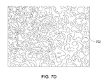
- FIG. 7D is a diagram of an exemplary anodized thin film surface topography as measured by an optical surface profiler.
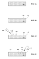
- FIGS. 8A-8C are diagrams of various exemplary views representative of a two-hundred times magnification photomicrograph of dark or black marking the metal structure according to one embodiment.
- FIG. 8D is a diagram of a top view representative of an exemplary darkness halftone pattern for marking the metal structure according to another embodiment.
- FIG. 9 is a diagram of a top view illustrating an exemplary lightness halftone pattern and a darkness halftone pattern for marking the metal structure according to another embodiment.
- FIG. 10A is a diagrammatic representation of an exemplary product housing.
- FIG. 10B illustrates the product housing having markings according to one exemplary embodiment.
- the invention pertains to techniques or processes for providing markings on products.
- the products have housings and the markings are to be provided on the housings.
- a housing for a particular product can include an outer housing surface and the markings can be provided on an outer housing surface so as to be visible from the outside of the housing.
- the markings provided on products can be textual and/or graphic.
- the markings can be formed with high resolution.
- the markings are also able to be light or dark (e.g., white or black), even on metal surfaces.
- the markings can be textual and/or graphic.
- the markings can be used to provide a product (e.g., a product's housing) with certain information.
- the marking can, for example, be use to label the product with various information.
- the text can provide information concerning the product (e.g., electronic device).
- the text can include one or more of: name of product, trademark or copyright information, design location, assembly location, model number, serial number, license number, agency approvals, standards compliance, electronic codes, memory of device, and the like).
- the graphic can pertain to a logo, a certification mark, standards mark or an approval mark that is often associated with the product.
- the marking can be used for advertisements to be provided on products.
- the markings can also be used for customization (e.g., user customization) of a housing of a product.
- CIE 1976 L*a*b* also known as CIELAB
- CIELAB CIE 1976 L*a*b*
- CIELAB describes colors visible to the human eye and was created to serve as a device independent model to be used as a reference.
- measurements in a format corresponding to the CIELAB standard may be made using a spectrophotometer, such as the COLOREYETM XTH spectrophotometer, which was sold by GretagMacbethTM. Similar spectrophotometers are available from X-RiteTM.
- FIG. 1 is a diagram of a marking state machine 100 according to one embodiment of the invention.
- the marking state machine 100 reflects three (3) basic states associated with marking an electronic device.
- the marking can mark a housing of an electronic device, such as a portable electronic device.
- the marking state machine 100 includes a substrate formation state 102 .
- a substrate can be obtained or produced.
- the substrate can represent at least a portion of a housing surface of an electronic device.
- the marking state machine 100 can transition to a protective surface state 104 .
- a protective surface can be formed or applied to at least one surface of the substrate.
- the protective surface can be used to protect the surface of the substrate.
- the protective surface can be a more durable surface than that of the surface of the substrate.
- the marking state machine 100 can transition to a marking state 106 .
- marking can be produced on the substrate (e.g., produced sub-surface to the protective surface) and/or produced in the protective surface.
- the marking can be provided with high resolution. Since the marking may be provided while maintaining smoothness of the protective surface, the marking has the advantage of not being perceptible of tactile detection on the surface.
- FIG. 2 is an illustration of a substrate 200 and an adjacently coupled protective thin film 202 .
- the substrate 200 may comprise metal, and in particular may comprise aluminum.
- the substrate may be substantially gray, and is depicted in the figures using stippling (i.e., pattern of small dots).
- the protective thin film 202 may comprise an anodized layer 202 .
- marking alterations 203 , 204 may include light or white alterations 203 (depicted with left to right hatching) that may be created by microfracturing of the thin film 202 while still maintaining a tactilely smooth surface of the thin film 202 ; and/or may include dark or black subsurface alterations 204 (depicted with cross hatching.)
- the sub-surface alterations 204 are provided below the thin film 202 and on a top surface 205 of the substrate 200 . Given that the thin film 202 is typically substantially translucent (e.g., clear), the sub-surface alterations 204 may be visible to a user through the thin film 202 .
- the sub-surface alterations 204 can provide dark or black markings on the substrate 200 . Since the dark or black markings are provided by the sub-surface alterations 204 , the markings are protected by the thin film 202 provided on the substrate 200 . Further, the sub-surface alterations may be made visible while maintaining the tactilely smooth surface of the thin film 202 .
- the substrate 200 can represent at least a portion of a housing of an electronic device.
- the marking being provided to the substrate 200 can provide text and/or graphics to an outer housing surface of an electronic device, such as a portable electronic device.
- the marking techniques are particularly useful for smaller scale portable electronic devices, such as electronic devices. Examples of handheld electronic devices include mobile telephones (e.g., cell phones), Personal Digital Assistants (PDAs), portable media players, remote controllers, pointing devices (e.g., computer mouse), game controllers, etc.
- FIGS. 3A-3C are flow diagrams of marking processes 300 A, 300 B, 300 C according to one embodiment.
- the marking processes 300 A, 300 B, 300 C can be performed on an electronic device that is to be marked.
- the marking processes 300 A, 300 B, 300 C are, for example, suitable for applying text or graphics to a housing (e.g., an outer housing surface) of an electronic device.
- the marking can be provided such that it is visible to users of the electronic device. However, the marking can be placed in various different positions, surfaces or structures of the electronic device.
- the marking processes 300 A, 300 B, 300 C can provide a metal structure for an article to be marked.
- the metal structure can pertain to a metal housing for an electronic device, such as a portable electronic device, to be marked.
- the metal structure can be formed of one metal layer.
- the metal structure can also be formed of multiple layers of different materials, where at least one of the multiple layers is a metal layer.
- the metal layer can, for example, be or include aluminum, titanium, niobium or tantalum.
- the process may begin with providing 302 A the metal structure for an article to be marked.
- material of a thin film may be adherently coupled 304 A adjacent to a surface of the metal structure, so as to provide a resulting structure having a lightness factor magnitude in a visible color space.
- the surface of the metal structure may be anodized 304 A to adherently couple material of the thin film (e.g. anodized layer.)
- the surface of the metal structure to be anodized 304 A is an outer or exposed metal surface of the metal structure.
- the outer or exposed surface can represent an exterior surface of the metal housing for the electronic device.
- the metal of the resulting structure may be gray and may be substantially visible through the thin film.
- the thin film may be selectively altered 306 A for increasing substantially the lightness factor magnitude of selected regions of the resulting structure, while substantially maintaining adherent coupling of the material of the thin film.
- the selectively altering 306 A of the thin film may increase the lightness factor magnitude to be substantially above fifty.
- the selected altered thin film regions showed an increased lightness factor magnitude, which was about 86.6 (which may be referred to as L*86.6).
- Increasing substantially the lightness factor magnitude may provide a substantially lightened visible appearance, and may provide a substantially white visible appearance, of the selected regions of the resulting structure.
- selectively altering 306 A the thin film may provide a substantially lightened visible appearance, and may provide a substantially white visible appearance, of the thin film of selected regions of the resulting structure. Accordingly, selectively altering 306 A the thin film may cause substantially white marking of the resulting structure.
- Selectively altering 306 A the thin film may be employed for marking the article by altered lightness characteristics of selected regions of the resulting structure, which may cause one or more light textual or graphical indicia to appear on the resulting structure.
- selectively altering 306 A the thin film for increasing substantially the lightness factor magnitude of selected regions of the resulting structure may comprise lightness halftoning, wherein the selected regions of the thin film may be arranged in a lightness halftone pattern.
- the thin film may comprises fracturing and, more particularly, may comprise microfracturing the thin film of selected regions of the resulting structure.
- the thin film can pertain to an anodized layer selectively altering the thin film may comprise selectively altering an anodized layer discussed previously herein.
- selectively altering the thin film may comprises fracturing and, more particularly, may comprise microfracturing the anodized layer of selected regions of the resulting structure.
- Selectively altering 306 A the thin film may comprise heating, and in particular may comprise laser heating of selected regions of the resulting structure.
- Selectively altering 306 A the thin film may comprise heating the metal surface of selected regions of the resulting structure.
- Selectively altering 306 A the thin film may comprise fracturing the thin film (e.g., anodized layer) adjacent to the surface of the metal structure, by heating the metal surface of selected regions of the resulting structure.
- the material of the thin film may be substantially more brittle than metal of the metal structure.
- the metal of the metal structure may be substantially more ductile than the material of the thin film.
- thermal expansion in response to heating of the metal of the metal structure may be substantially greater than thermal expansion in response heating of the thin film.
- laser selection and operation may be controlled so that laser heating by electron-phonon coupling may predominate over other laser effects; and electron-phonon coupling of the metal of the metal structure may be substantially higher than electron-phonon coupling of the thin film, so that laser heating of the metal of the metal structure may be substantially greater than laser heating of the thin film.
- selectively heating of the metal surface of selected regions of the resulting structure may selectively alter 306 A the thin film by fracturing the thin film adjacent to the surface of the metal structure.
- the foregoing different responses to heating of the metal and the adherently coupled thin film may contribute to stresses in excess of fracture tolerance of the thin film, which may result in fracturing of the thin film.
- aluminum oxide of an anodized layer may be substantially more brittle than aluminum metal of the metal structure.
- the aluminum metal of the metal structure may be substantially more ductile than the aluminum oxide of the anodized layer.
- thermal expansion in response to heating of the aluminum metal of the metal structure may be substantially greater than thermal expansion in response to heating of the aluminum oxide of the anodized layer.
- electron-phonon coupling of the aluminum metal of the metal structure may be substantially higher than electron-phonon coupling of the aluminum oxide of the anodized layer, so that laser heating of the aluminum metal of the metal structure may be substantially greater than laser heating of the aluminum oxide of the anodized layer.
- selectively heating the aluminum metal surface of selected regions of the resulting structure may selectively alter 306 A the anodized layer by fracturing (e.g., microfracturing) the anodized layer adjacent to the surface of the metal structure.
- fracturing e.g., microfracturing
- the foregoing different responses to heating of the aluminum metal and the adherently coupled aluminum oxide of the anodized layer may contribute to stresses in excess of fracture tolerance of the anodized layer, which may result in fracturing of the anodized layer.
- Substantially maintaining adherent coupling of the material of the thin film to the metal substrate may substantially avoid etching of the material of the thin film material.
- substantially maintaining adherent coupling of the aluminum oxide material of an anodized layer may substantially avoid etching the aluminum oxide material of the anodized layer when being selectively altered 306 A.
- selectively altering 306 A the thin film may maintain a tactilely smooth surface of the thin film.
- the thin film may be selectively altered by microfracturing the thin film, while maintain the tactilely smooth surface of the thin film.
- measurements by an optical surface profiler may show substantially no change in thin film surface topology due to selectively altering 306 A the thin film, while also substantially maintaining adherent coupling of the material of the thin film.
- microfracturing the thin film, while substantially maintaining adherent coupling of the material of the thin film may show substantially no change in thin film surface topology in measurements by the optical surface profiler.
- the selectively altering 306 A of the thin film may induce micro-features therein (e.g., microfracturing) but can doe so without destruction of the thin layer.
- Selectively altering 306 A the thin film may comprise directing a laser output through the thin film adjacent to a surface of the metal structure, and towards the surface of the metal structure.
- the laser output may be controlled for substantially maintaining adherent coupling of the material of the thin film, so as to avoid various deleterious effects, while white marking select portions of the thin film via micro-fracturing.
- the laser output may be controlled so as to maintain the tactilely smooth surface of the thin film.
- the laser output may be controlled so as to substantially avoid laser etching of the thin film.
- the laser output may be controlled so as to substantially avoid ablation of the metal or thin film.
- substantially maintaining adherent coupling 306 A of the material of the thin film may comprise substantially avoiding laser etching of the material of the thin film material.
- substantially maintaining adherent coupling 306 A of the material of the thin film may also comprise substantially avoiding ablation of the material of the thin film.
- the thin film may employ a suitably selected and operated laser for providing the laser output.
- a suitably selected and operated laser for providing the laser output.
- one specific suitable laser may be operated in substantially continuous wave (CW) mode at a selectively limited power of two (2) Watts and at an infrared wavelength (10.6 micron wavelength), such as the Alltec laser model CO2 LC100, which may be obtained from Alltec GmbH, An der Trave 27-31, 23923 Selmsdorf, Germany.
- Accompanying optics may be used to provide a laser output spot size within a range from approximately seventy (70) microns to approximately one-hundred (100) microns.
- irradiance For a spot of about 0.00005 square centimeters, selectively limits irradiance to approximately forty (40) Kilo-Watts per square centimeter, for selectively altering 306 A the thin film, while substantially maintaining adherent coupling of the material of the thin film. It should be understood that the foregoing are approximate exemplary laser operating parameters, and that various other laser operating parameters may be suitable for selectively altering 306 A the thin film, while substantially maintaining adherent coupling of the material of the thin film. Laser output spot size and/or irradiance may be selected for selectively altering 306 A the thin film, while substantially maintaining adherent coupling of the material of the thin film. The foregoing may substantially avoid etching or ablation of the material of the thin film material; may maintain a tactilely smooth surface of the thin film; and/or may substantially avoid changes in thin film surface topology.
- Selectively altering 306 A the thin film may comprise directing the laser output towards the surface of the metal structure, while limiting power of the laser output, so as to substantially avoid ablation of the metal of the metal structure.
- the metal may be characterized by an ablation threshold irradiance, and the laser output may have an irradiance that is approximately less than the ablation threshold irradiance of the metal, for substantially avoiding ablation of the metal of the metal structure.
- the process may begin with providing 302 B the metal structure for an article to be marked, wherein the metal may comprise aluminum metal.
- the article may be anodized for creating 304 B an anodized layer.
- light scattering points may be created 306 B within the anodized layer, for example, by microfracturing the anodized layer.
- the light scattering points may provide a white or translucent appearance above the aluminum metal, which is disposed beneath the anodized layer.
- the marking process 300 B shown in FIG. 3B can end.
- the process may begin with providing 302 C the metal structure for an article to be marked.
- material of a thin film may be adherently coupled 304 C adjacent to a surface of the metal structure, so as to provide a resulting structure having a lightness factor magnitude in a visible color space.
- the metal of the resulting structure may be gray and may be substantially visible through the thin film.
- the surface of the metal structure may be anodized 304 C to adherently couple material of the thin film (e.g. anodized layer).
- the surface of the metal structure can be anodized 304 C.
- surface characteristics of selected regions of the surface of the metal structure may be selectively altered 306 C, for example may be selectively roughened, for decreasing substantially the lightness factor magnitude of selected regions of the resulting structure, while substantially maintaining adherent coupling of the material of the thin film.
- selective roughening may be ultrasmall scale roughening, for example the ultrasmall scale roughening may comprise nanoscale roughening.
- Selectively altering 306 C of the metal surface may decrease the lightness factor magnitude to be substantially below fifty.
- the selected altered metal surface regions showed a decreased lightness factor magnitude, which may range in magnitude from about twenty to about thirty (which may be referenced as about “L*20” to about “L*30”.)
- Decreasing substantially the lightness factor magnitude may provide a substantially darkened visible appearance, and may provide a substantially black visible appearance, of the selected regions of the resulting structure.
- selectively altering 306 C the metal surface may provide a substantially darkened visible appearance, and may provide a substantially black visible appearance, of the metal surface of selected regions of the resulting structure. Accordingly, selectively altering 306 C the metal surface may cause substantially black marking of the resulting structure.
- Selectively altering 306 C the metal surface may be employed for marking the article by altered darkness characteristics of selected regions of the resulting structure, which can be used to form one or more dark textual or graphical indicia to appear on the resulting structure. Further, as will be discussed in greater detail subsequently herein, selectively altering 306 C the metal surface for decreasing substantially the lightness factor magnitude of selected regions of the resulting structure may comprise darkness halftoning, wherein the selected regions of the metal surface may be arranged in a darkness halftone pattern.
- Substantially maintaining adherent coupling of the material of the thin film may substantially avoid etching or ablation of the material of the thin film material.
- the thin film can be a layer of aluminum oxide material.
- substantially maintaining adherent coupling of an aluminum oxide material of an anodized layer may substantially avoid etching or ablation the aluminum oxide material of the anodized layer.
- selectively altering 306 C the metal surface may substantially maintain a tactilely smooth surface of the thin film. In such case, the metal surface may be selectively altered beneath the thin film, while the thin film remains substantially in place, and while substantially maintaining the tactilely smooth surface of the thin film.
- Selectively altering 306 C the metal surface may comprise directing a laser output through the thin film (e.g., anodized layer) adjacent to the surface of the metal structure, and towards the surface of the metal structure.
- the surface of the metal structure to be anodized is an outer or exposed metal surface of the metal structure.
- the outer or exposed surface with anodized layer typically represents an exterior surface of the metal housing for the electronic device.
- surface characteristics of selected portions of an inner unanodized surface of the metal structure may be altered 306 C.
- the inner unanodized surface may be part of the metal layer that was anodized, or may be part of another metal layer that was not anodized.
- the laser output may be controlled for substantially maintaining adherent coupling of the material of the thin film, so as to avoid various deleterious effects, while black marking the metal surface.
- the laser output may be controlled so as to maintain substantially the tactilely smooth surface of the thin film.
- the laser output may be controlled so as to substantially avoid laser etching of the thin film.
- the laser output may be controlled for substantially avoiding ablation of the metal or thin film.
- substantially maintaining adherent coupling 306 C of the material of the thin film may comprise substantially avoiding laser etching of the material of the thin film material.
- substantially maintaining adherent coupling 306 C of the material of the thin film may also comprise substantially avoiding ablation of the material of the thin film.
- Selectively altering 306 C the metal surface may employ a suitably selected and operated laser for providing the laser output.
- the surface characteristics can be altered 306 C using a laser, such as an infrared wavelength laser (e.g., picosecond pulsewidth infrared laser or nanosecond pulsewidth infrared laser).
- a laser such as an infrared wavelength laser (e.g., picosecond pulsewidth infrared laser or nanosecond pulsewidth infrared laser).
- picosecond pulsewidth infrared laser e.g., picosecond pulsewidth infrared laser or nanosecond pulsewidth infrared laser
- one specific suitable laser is a six (6) Watt infrared wavelength picosecond pulsewidth laser at 1000 KHz with a scan speed of 50 mm/sec. While such picosecond pulsewidth laser may provide many advantages, it may be more expensive than an alternative nanosecond pulsewidth laser.
- an example of a suitable alternative laser is a ten (10) Watt infrared wavelength nanosecond pulsewidth lasers at 40 KHz with a scan speed of 20 mm/sec.
- Fluence of pulses of the laser may be selected so as to be approximately less than an ablation threshold fluence that characterizes the metal. Selection of the laser fluence may be for substantially avoiding ablation of the metal. Further, fluence of pulses of the laser may be selected so as to be greater than a damage fluence that characterizes the metal, so as to provide for altering surface characteristics of the selected portions of the inner unanodized surface of the metal structure.
- Accompanying optics may be used to provide a laser output spot size within a selected range, as discussed in greater detail subsequently herein.
- Laser output spot size and/or irradiance may be selected for selectively altering 306 C the metal surface, while substantially maintaining adherent coupling of the material of the thin film.
- the foregoing may substantially avoid etching or ablation of the material of the thin film material; may substantially maintain a tactilely smooth surface of the thin film; and/or may substantially avoid changes in thin film surface topology.
- Selectively altering 306 C the metal surface may comprise directing the laser output towards the surface of the metal structure, while limiting power of the laser output, so as to substantially avoid ablation of the metal of the metal structure.
- the metal may be characterized by an ablation threshold irradiance and/or ablation threshold fluence, and the laser output may have an irradiance and/or fluence that is approximately less than the ablation threshold irradiance and/or ablation threshold fluence of the metal, for substantially avoiding ablation of the metal of the metal structure.
- the process 300 B shown in FIG. 3B and the process 300 C shown in FIG. 3C can be considered embodiment of the process 300 A shown in FIG. 3A .
- FIGS. 4A-4D are diagrams illustrating marking of a metal structure according to one embodiment.
- FIG. 4A illustrates a base metal structure 400 .
- the base metal structure 400 can be formed of aluminum, titanium, niobium or tantalum.
- the base metal structure may be substantially gray, and is depicted in the FIGS. 4A-4D using stippling.
- FIG. 4B illustrates the base metal structure 400 after an upper surface has been anodized to form an anodized surface 402 .
- the thickness of the anodized surface 402 can, for example, be about 5-20 microns.
- the anodized surface 402 can be considered a thin film, which represents a coating or layer.
- Aluminum oxide material of the anodized surface may be adherently (e.g., chemically bonded) coupled adjacent to an inner unanodized surface 406 of the metal structure 400 .
- FIG. 4C illustrates light (e.g., white) alterations 403 (depicted with left to right hatching) that may be created by microfracturing of the anodized surface 402 , while substantially maintaining adherent coupling of the aluminum oxide material of the anodized surface 402 adjacent to the inner unanodized surface 406 of the metal structure 400 .
- the light alterations 403 are formed by suitably selected optical energy 407 produced by a suitably selected and operated laser 409 (as discussed in detail previously herein with respect to light or white marking).
- the altered surfaces 403 combine to provide marking of the metal structure 400 .
- the light alterations 403 appear to be light, and thus when selectively formed can provide light or white marking.
- the light or white marking can also be provided in lightness halftone arranged in a suitably selected lightness halftone pattern. If the anodized surface is dyed or colored, the markings may appear in different colors.
- the laser 407 may include a galvanometer mirror or other arrangement for raster scanning a spot of the optical energy over the anodized surface 402 , so as to form the light alterations into a rasterized depiction of the light (e.g., white) marking indicia.
- Suitable pitch between raster scan lines of the scanning spot for the light (e.g., white) marking may be selected.
- pitch between raster scan lines may be about fifty (50) microns, and scan speed may be about two hundred (200) millimeters per second.
- FIG. 4D illustrates altered surfaces 404 (depicted with cross hatching) being selectively formed on an inner unanodized surface 406 , while substantially maintaining adherent coupling of the aluminum oxide material of the anodized surface 402 adjacent to the inner unanodized surface 406 of the metal structure 400 .
- Such altered structures 404 are formed for dark (e.g., black) marking by suitably selected optical energy 408 produced by a suitably selected and operated laser 410 (as discussed in detail previously herein with respect to dark or black marking).
- the altered surfaces 404 combine to provide dark (e.g., black) marking of the metal structure 400 .
- the altered surfaces 404 appear to be dark or black and thus when selectively formed can provide dark marking.
- the resulting dark marking is visible through the anodized surface 402 which can be substantially translucent. If the anodized surface 402 is primarily clear, the resulting marking can be appear as dark (e.g., black).
- the marking can also be provided in darkness halftone in a suitably selected darkness halftone pattern. If the anodized surface is dyed or colored, the dark markings may appear in different colors.
- Fluence of the optical energy may be above the damage threshold fluence for the base metal structure, for forming the altered structures 404 .
- fluence of the optical energy that forms the altered structures 404 on the altered surfaces of the base metal structure may be selected to be approximately below the ablation threshold fluence for the base metal structure, so as to avoid deleterious effects, for example, predominant ablative stripping of the anodized surface or the base metal structure.
- predominant fracturing of the anodized surface, or predominant delaminating of the anodized surface away from the base metal structure may be substantially avoided by selectively limiting fluence of the optical energy that forms the altered structures.
- Fluence of the optical energy that forms the altered structures 404 on the altered surfaces of the base metal structure may be selected so that non-ablative laser-material interactions such as heating, surface melting, surface vaporization and/or plasma formation predominate over any ablation.
- ablation which may be characterized by direct evaporation the metal, in an explosive boiling that forms a mixture of energetic gases comprising atoms, molecules, ions and electrons, may not predominate over non-ablative laser-material interactions, such as heating, surface melting, surface vaporization and/or plasma formation.
- the laser 410 may include a galvanometer mirror or other arrangement for raster scanning a spot of the optical energy over the inner unanodized surface 406 , so as to form the altered structures into a rasterized depiction of the marking indicia. Suitable pitch between raster scan lines of the scanning spot for the black marking may be selected. For example, a suitable pitch may be a fine pitch of about thirteen (13) microns.
- the laser 410 may further include optics for contracting or expanding size of the spot of the optical energy, by focusing or defocusing the spot. Expanding size of the spot, by defocusing the spot may be used to select fluence of the optical energy.
- expanding size of the spot may select fluence of the optical energy below the ablation threshold fluence for the base metal structure.
- Spot size of the optical energy for the nanosecond class laser mentioned previously herein may be within a range from approximately fifty (50) microns to approximately one hundred (100) microns; and spot size may be about seventy (70) microns.
- FIG. 5 is a table illustrating exemplary laser operation parameters for dark (e.g., black) marking of a metal structure according to one embodiment.
- the table of FIG. 4D shows examples of various suitable laser models which may be used for marking the metal structure.
- the FOBA DP20GS is a Diode Pumped Solid State Neodymium-Doped Yttrium Orthovanadate (DPSS YVO4) type laser, which is available from FOBA Technology and Services GmbH, having offices at 159 Swanson Road, Boxborough, Mass.
- the SPI 12W/SM AND SPI 20W/SM are fiber type lasers, which are available from SPI Lasers UK, having offices at 4000 Burton Drive, Santa Clara, Calif.
- the Lumera is a picosecond type laser, which is available from LUMERA LASER GmbH, having an office at Opelstr 10, 67661 Kaiserslautern, Germany. It should be understood that the table of FIG. 5 shows approximate exemplary laser operating parameters, and that various other laser operating parameters may be selected to provide the fluence of the optical energy that forms the altered structures for dark or black marking of a base metal structure, wherein the fluence may be selected to be approximately below the ablation threshold fluence for the base metal structure.
- FIG. 6 is a diagram further illustrating exemplary laser operation parameters for dark (e.g., black) marking a metal structure according to one embodiment.
- irradiance of Laser Light Intensity in Watts per square centimeter is shown along a vertical axis, while Interaction Time of each pulse of the laser light (optical energy) with the metal structure is shown in fractions of a second along a horizontal axis.
- diagonal lines of constant fuence of approximately ten (10) milli-Joules per square centimeter and of approximately one (1) Joule per square centimeter are shown in FIG. 6 .
- a temperature “T” of the metal structure may not substantially exceed a critical temperature for ablation of the metal structure.
- T a temperature “T” of the metal structure may not substantially exceed a critical temperature for ablation of the metal structure.
- a stippled region of exemplary excessively high laser light intensity is shown in FIG. 6 , along with a descriptive legend T>T critical for ablation.
- FIG. 6 further shows a cross hatched region of suggested approximate parameters for formation of the altered structures for the dark or black marking.
- FIG. 7A is a diagram of a top view of an exemplary two-hundred times magnification photomicrograph of light (e.g., white) marking of an anodized thin film surface 702 of a metal structure according to one embodiment.
- the anodized thin film surface 702 may be substantially clear or translucent, however, as shown in FIG. 7A , slight curved island surface features of the anodized thin film surface 702 may be seen under the two-hundred times magnification.
- the anodized thin film surface 702 may include light alterations 703 (depicted with left to right hatching) that may be created by microfracturing of the anodized thin film surface 702 , while substantially maintaining adherent coupling of the aluminum oxide material of the anodized thin film surface adjacent to the inner unanodized surface of the metal structure.
- the metal structure may appear gray and may be visible through an unaltered substantially clear or transparent remainder portion of the anodized thin film surface 702 .
- Light scattering points may be created by microfracturing the anodized thin film surface for the light alterations 703 , which may significantly obscure visibility of the metal structure through the anodized thin film surface.
- FIG. 7B is a diagram of a top view of an exemplary lightness halftone pattern 713 of light (e.g., white) alterations 713 (depicted with left to right hatching), which may be created by microfracturing of the anodized thin film surface 702 .
- the metal structure may appear gray and may be visible through the unaltered substantially clear or transparent remainder portion of the anodized thin film surface 702 .
- Size of the light alterations 713 , as well as spaced apart arrangement of the light alterations 713 in the lightness halftone pattern may be selected so as to provide a desired halftoning appearance.
- FIG. 7C is a diagram of a top view of an exemplary one thousand times magnification scanning electron micrograph of a microfractured region of an anodized thin film surface of a metal structure, for effecting the light or white marking of the metal structure.
- Scanning electron microscopy can reveal details and features smaller than wavelengths of visible light. For example, anodic pores having diameters on the order of ten nanometers and extending into the anodized thin film surface are shown in FIG. 7C .
- the scanning electron micrograph reveals the structure of microfractures 716 , having dimensions on a scale of less than one micron, wherein the microfractures 716 may produce substantial scattering of light at visible wavelengths.
- One slight curved island surface features 718 of the anodized thin film surface 702 is shown under one thousand times magnification in the diagram depiction of the scanning electron micrograph of FIG. 7C .
- FIG. 7D is a diagram of an exemplary anodized thin film surface topography of the anodized thin film 702 as measured by an optical surface profiler, which at low magnification (e.g., less than two-hundred times magnification) may show substantially no perceptible change in the thin film surface topology for regions of light marking alterations, relative to remainder unaltered regions, without light marking alterations. Measurements, for example, can be made using ADE Phase Shift MicroXAM Optical interferometric profiler. Depictions of slight curved island surface features are shown in FIG. 7D for the anodized thin film surface topography of the anodized thin film 702 . Typically, height magnitude of the slight curved island surface features may be less than about a couple of microns.
- substantially maintaining adherent coupling of the material of the anodized thin film 702 may substantially avoid etching of the material of the thin film material. More particularly, substantially maintaining adherent coupling of the aluminum oxide material of the anodized thin film 702 may substantially avoid etching the aluminum oxide material of the anodized thin film 702 .
- measurements by the optical surface profiler may show substantially no change in the anodized thin film surface topology due to selectively altering the thin film, while substantially maintaining adherent coupling of the material of the thin film.
- microfracturing the anodized thin film, while substantially maintaining adherent coupling of the material of the thin film may show substantially no change in thin film surface topology in measurements by the optical surface profiler.
- FIGS. 8A-8C are diagrams of various exemplary views representative of a two-hundred times magnification photomicrograph of dark (e.g., black) marking the metal structure according to one embodiment.
- Base metal structure 800 may appear gray, and is depicted in FIGS. 8A-8C using stippling.
- the anodized thin film surface 802 is shown exploded away from the inner unanodized surface 806 of the base metal structure 800 in isometric view, so as to show clearly altered structures 804 (which are particularly highlighted using cross hatching).
- the altered structures 804 may correspond to selected roughened regions.
- the selected roughened regions may comprise ultrasmall scale roughening in selected regions of the inner unanodized surface 806 of the base metal structure 800 .
- the ultrasmall scale roughening may comprise nanoscale roughening.
- the anodized thin film surface 802 , the altered structures 804 and the inner unanodized surface 806 of the base metal structure 400 are shown in a collapsed isometric view in FIG. 8B , and in a top view in FIG. 8C .
- the anodized thin film surface 802 may appear substantially optically transparent as shown in FIGS. 8A through 8C ; however, slight curved island surface features of the anodized thin film surface 802 may be seen under the two-hundred times magnification. Further, FIGS. 8A through 8C show a stepped plateau feature of the anodized thin film surface 802 , which may be due to elevation by the altered structures 804 , or may be due to an increase in volume contributed by the altered structures 804 . A thickness of the stepped plateau feature may be slight, and may be about two to four microns.
- selectively altering the unanodized metal surface 806 to produce the altered structures 804 substantially maintains adherent coupling of the material of the anodized thin film surface 802 .
- the foregoing may substantially avoid etching or ablation of the material of the thin film material; may substantially maintain a tactilely smooth surface of the thin film; and/or may substantially avoid changes in thin film surface topology.
- FIG. 8D is a diagram of a top view of an exemplary darkness halftone pattern 814 (depicted with cross hatching) for marking the metal structure according to another embodiment.
- a metal structure may appear gray and may be visible through the unaltered substantially clear or transparent remainder portion of the anodized thin film surface 802 .
- Size of the dark (e.g., black) alterations 814 , as well as spaced apart arrangement of the dark alterations 814 in the darkness halftone pattern may be selected so as to provide a desired halftoning appearance.
- FIG. 9 is a diagram of a top view illustrating an exemplary lightness halftone pattern 913 (depicted with left to right hatching) and a darkness halftone pattern 914 (depicted with cross hatching) for marking the metal structure according to another embodiment.
- a metal structure may appear gray and may be visible through the unaltered substantially clear or transparent remainder portion of an anodized thin film surface 902 .
- suitable selections may be made for sizes of the alterations 913 , 914 as well as spaced apart arrangements of the alterations 913 . 914 in the respective lightness and darkness halftone patterns.
- FIG. 10A is a diagrammatic representation of an exemplary product housing 1000 .
- the housing 1000 may be formed using aluminum or another suitable metal.
- the housing 1000 may be a housing that is to be a part of an overall assembly.
- the housing 1000 can be a bottom of a cell phone assembly or portable media player, or can be a portion of a housing for a personal computer or any other device having a metal housing.
- FIG. 10B illustrates the product housing 1000 having markings 1002 according to one exemplary embodiment.
- the markings 1002 can be light or white markings in accordance with the light or white markings discussed previously herein.
- the markings 1002 can be dark or black markings produced on a sub-surface of the product housing 1000 in accordance with the dark or black markings discussed previously herein.
- the labeling includes a logo graphic 1004 , serial number 1006 , model number 1008 , and certification/approval marks 1010 and 1012 .
- light (e.g., white) or dark (e.g., black) colors for marking other colors or shades can be provided by halftoning and/or dyes.
- the marking processes described herein are, for example, suitable for applying text or graphics to a housing surface (e.g., an outer housing surface) of a device, such as an electronic device.
- the marking processes are, in one embodiment, particularly well-suited for applying text and/or graphics to an outer housing surface of a portable electronic device.
- portable electronic devices include mobile telephones (e.g., cell phones), Personal Digital Assistants (PDAs), portable media players, portable computers, remote controllers, pointing devices (e.g., computer mouse), game controllers, etc.
- PDAs Personal Digital Assistants
- portable media players portable media players
- portable computers portable computers
- remote controllers pointing devices
- pointing devices e.g., computer mouse
- game controllers e.g., etc.
- the portable electronic device can further be a hand-held electronic device.
- the term hand-held generally means that the electronic device has a form factor that is small enough to be comfortably held in one hand.
- a hand-held electronic device may be directed at one-handed operation or two-handed operation.
- one-handed operation a single hand is used to both support the device as well as to perform operations with the user interface during use.
- two-handed operation one hand is used to support the device while the other hand performs operations with a user interface during use or alternatively both hands support the device as well as perform operations during use.
- the hand-held electronic device is sized for placement into a pocket of the user. By being pocket-sized, the user does not have to directly carry the device and therefore the device can be taken almost anywhere the user travels (e.g., the user is not limited by carrying a large, bulky and often heavy device).
- One advantage of the invention is that durable, high precision markings can be provided to product housings.
- the markings being provided on a product housing that not only have high resolution and durability but also provide a smooth and high quality appearance.
- Another advantage is that the marking techniques are effective for surfaces that are flat or curved.
Landscapes
- Chemical & Material Sciences (AREA)
- Engineering & Computer Science (AREA)
- Chemical Kinetics & Catalysis (AREA)
- Electrochemistry (AREA)
- Materials Engineering (AREA)
- Metallurgy (AREA)
- Organic Chemistry (AREA)
- Ceramic Engineering (AREA)
- Physics & Mathematics (AREA)
- Optics & Photonics (AREA)
- Laser Beam Processing (AREA)
- Thermal Transfer Or Thermal Recording In General (AREA)
Abstract
Techniques or processes for providing markings on products are disclosed. In one embodiment, the products have housings and the markings are to be provided on the housings. For example, a housing for a particular product can include an outer housing surface and the markings can be provided in the outer housing surface so as to be visible from the outside of the housing.
Description
This application is a continuation-in-part of U.S. application Ser. No. 12/895,384, filed Sep. 30, 2010 and entitled “SUB-SURFACE MARKING OF PRODUCT HOUSINGS,” which is hereby incorporated herein by reference, which in turn is a continuation-in-part of U.S. application Ser. No. 12/643,772, filed Dec. 21, 2009 and entitled “SUB-SURFACE MARKING OF PRODUCT HOUSINGS,” which is hereby incorporated herein by reference, which claims priority benefit of U.S. Provisional Application No. 61/252,623, filed Oct. 16, 2009 and entitled “SUB-SURFACE MARKING OF PRODUCT HOUSINGS,” which is hereby incorporated herein by reference.
Field of the Invention
The present invention relates to marking products and, more particularly, marking housings of electronic devices.
Description of the Related Art
Consumer products, such as electronic devices, have been marked with different information for many years. For example, it is common for electronic devices to be marked with a serial number, model number, copyright information and the like. Conventionally, such marking is done with an ink printing or stamping process. Although conventional ink printing and stamping is useful for many situations, such techniques can be inadequate in the case of handheld electronic devices. The small form factor of handheld electronic devices, such as mobile phones, portable media players and Personal Digital Assistants (PDAs), requires that the marking be very small. In order for such small marking to be legible, the marking must be accurately and precisely formed. Unfortunately, however, conventional techniques are not able to offer sufficient accuracy and precision. Thus, there is a need for improved techniques to mark products.
The invention pertains to techniques or processes for providing markings on products. In one embodiment, the products have housings and the markings are to be provided on the housings. For example, a housing for a particular product can include an outer housing surface and the markings can be provided on the outer housing surface so as to be visible from the outside of the housing. The markings provided on products can be textual and/or graphic. The markings can be formed with high resolution. The markings are also able to be light or dark (e.g., white or black), even on metal surfaces.
In general, the markings (also referred to as annotations or labeling) provided on products according to the invention can be textual and/or graphic. The markings can be used to provide a product (e.g., a product's housing) with certain information. The marking can, for example, be use to label the product with various information. When a marking includes text, the text can provide information concerning the product (e.g., electronic device). For example, the text can include one or more of: name of product, trademark or copyright information, design location, assembly location, model number, serial number, license number, agency approvals, standards compliance, electronic codes, memory of device, and the like). When a marking includes a graphic, the graphic can pertain to a logo, a certification mark, standards mark or an approval mark that is often associated with the product. The marking can be used for advertisements to be provided on products. The markings can also be used for customization (e.g., user customization) of a housing of a product.
The invention can be implemented in numerous ways, including as a method, system, device, or apparatus. Several embodiments of the invention are discussed below.
As a method for marking an article, one embodiment can, for example, include at least providing a metal structure for the article, adherently coupling material of a thin film adjacent to a surface of the metal structure, so as to provide a resulting structure having a lightness factor magnitude in a visible color space, and selectively altering the thin film for substantially increasing the lightness factor magnitude of selected regions of the resulting structure, while substantially maintaining adherent coupling of the material of the thin film.
As another method for marking an article, one embodiment can, for example, include at least: providing a metal structure for the article, adherently coupling material of a thin film adjacent to a surface of the metal structure, so as to provide a resulting structure having a lightness factor magnitude in a visible color space, and altering the lightness factor magnitude of selected regions of the resulting structure, while substantially maintaining adherent coupling of the material of the thin film.
As another method, one embodiment can, for example, include at least providing an article comprising aluminum metal, anodizing the article to create an anodized layer; and creating light scattering points within the anodized layer, the light scattering points providing a white or translucent appearance above the aluminum metal, which is disposed beneath the anodized layer.
As another embodiment, the electronic device housing can, for example, include at least a metal structure having a lightness factor magnitude in a visible color space; a substantially translucent thin film coupled adjacent to a surface of the metal structure, so as to provide a resulting structure; and textual or graphical marking indicia on the electronic device housing selected altered regions of the resulting structure having a lightness factor magnitude substantially different than that of the metal structure.
As an electronic device housing, one embodiment can, for example, include at least a metal structure, a thin film coupled adjacent to a surface of the metal structure, and selectively fractured regions of the thin film that are substantially smooth.
As another electronic device housing, one embodiment can, for example, include at least a housing structure including at least an outer portion and an inner portion, the outer portion being anodized and the inner portion being unanodized, and selectively altered surface regions formed within the outer portion of the housing structure. The altered surface regions provide marking of the electronic device housing.
Other aspects and advantages of the invention will become apparent from the following detailed description taken in conjunction with the accompanying drawings which illustrate, by way of example, the principles of the invention.
The invention will be readily understood by the following detailed description in conjunction with the accompanying drawings, wherein like reference numerals designate like structural elements, and in which:
The invention pertains to techniques or processes for providing markings on products. In one embodiment, the products have housings and the markings are to be provided on the housings. For example, a housing for a particular product can include an outer housing surface and the markings can be provided on an outer housing surface so as to be visible from the outside of the housing. The markings provided on products can be textual and/or graphic. The markings can be formed with high resolution. The markings are also able to be light or dark (e.g., white or black), even on metal surfaces.
In general, the markings (also referred to as annotations or labeling) provided on products can be textual and/or graphic. The markings can be used to provide a product (e.g., a product's housing) with certain information. The marking can, for example, be use to label the product with various information. When a marking includes text, the text can provide information concerning the product (e.g., electronic device). For example, the text can include one or more of: name of product, trademark or copyright information, design location, assembly location, model number, serial number, license number, agency approvals, standards compliance, electronic codes, memory of device, and the like). When a marking includes a graphic, the graphic can pertain to a logo, a certification mark, standards mark or an approval mark that is often associated with the product. The marking can be used for advertisements to be provided on products. The markings can also be used for customization (e.g., user customization) of a housing of a product.
Appearance of the housing, and in particular appearance of markings on the housing may be described using CIE 1976 L*a*b* (also known as CIELAB), which is a color space standard specified by the International Commission on Illumination (French Commission internationale de l'éclairage). CIELAB describes colors visible to the human eye and was created to serve as a device independent model to be used as a reference. The three coordinates of the CIELAB standard represent: 1) the lightness factor magnitude of the color (L*=0 yields ultimate black and L*=100 indicates diffuse ultimate white, 2) its position between red/magenta and green (a*, negative values indicate green while positive values indicate magenta) and 3) its position between yellow and blue (b*, negative values indicate blue and positive values indicate yellow). As discussed in further detail subsequently herein, measurements in a format corresponding to the CIELAB standard may be made using a spectrophotometer, such as the COLOREYE™ XTH spectrophotometer, which was sold by GretagMacbeth™. Similar spectrophotometers are available from X-Rite™.
Exemplary embodiments of the invention are discussed below with reference to FIGS. 1-10B . However, those skilled in the art will readily appreciate that the detailed description given herein with respect to these figures is for explanatory purposes as the invention extends beyond these limited embodiments.
The marking state machine 100 includes a substrate formation state 102. At the substrate formation state 102, a substrate can be obtained or produced. For example, the substrate can represent at least a portion of a housing surface of an electronic device. Next, the marking state machine 100 can transition to a protective surface state 104. At the protective surface state 104, a protective surface can be formed or applied to at least one surface of the substrate. The protective surface can be used to protect the surface of the substrate. For example, the protective surface can be a more durable surface than that of the surface of the substrate. Next, the marking state machine 100 can transition to a marking state 106. At the marking state 106, marking can be produced on the substrate (e.g., produced sub-surface to the protective surface) and/or produced in the protective surface. The marking can be provided with high resolution. Since the marking may be provided while maintaining smoothness of the protective surface, the marking has the advantage of not being perceptible of tactile detection on the surface.
As shown in FIG. 2 , marking alterations 203, 204 may include light or white alterations 203 (depicted with left to right hatching) that may be created by microfracturing of the thin film 202 while still maintaining a tactilely smooth surface of the thin film 202; and/or may include dark or black subsurface alterations 204 (depicted with cross hatching.) The sub-surface alterations 204 are provided below the thin film 202 and on a top surface 205 of the substrate 200. Given that the thin film 202 is typically substantially translucent (e.g., clear), the sub-surface alterations 204 may be visible to a user through the thin film 202.
Accordingly, the sub-surface alterations 204 can provide dark or black markings on the substrate 200. Since the dark or black markings are provided by the sub-surface alterations 204, the markings are protected by the thin film 202 provided on the substrate 200. Further, the sub-surface alterations may be made visible while maintaining the tactilely smooth surface of the thin film 202.
The substrate 200 can represent at least a portion of a housing of an electronic device. The marking being provided to the substrate 200 can provide text and/or graphics to an outer housing surface of an electronic device, such as a portable electronic device. The marking techniques are particularly useful for smaller scale portable electronic devices, such as electronic devices. Examples of handheld electronic devices include mobile telephones (e.g., cell phones), Personal Digital Assistants (PDAs), portable media players, remote controllers, pointing devices (e.g., computer mouse), game controllers, etc.
The marking processes 300A, 300B, 300C can provide a metal structure for an article to be marked. The metal structure can pertain to a metal housing for an electronic device, such as a portable electronic device, to be marked. The metal structure can be formed of one metal layer. The metal structure can also be formed of multiple layers of different materials, where at least one of the multiple layers is a metal layer. The metal layer can, for example, be or include aluminum, titanium, niobium or tantalum.
In accordance with the marking process 300A shown in FIG. 3A , the process may begin with providing 302A the metal structure for an article to be marked. After the metal structure has been provided 302A, material of a thin film may be adherently coupled 304A adjacent to a surface of the metal structure, so as to provide a resulting structure having a lightness factor magnitude in a visible color space. In one embodiment, the surface of the metal structure may be anodized 304A to adherently couple material of the thin film (e.g. anodized layer.) Typically, the surface of the metal structure to be anodized 304A is an outer or exposed metal surface of the metal structure. For example, the outer or exposed surface can represent an exterior surface of the metal housing for the electronic device.
Given that the thin film (e.g., anodized layer) is typically substantially translucent (e.g., clear), the metal of the resulting structure may be gray and may be substantially visible through the thin film. Measuring lightness factor magnitude of the resulting structure using a spectrophotometer, in accordance with the CIELAB standard scale, the lightness factor magnitude may be about 68 (which may be referred to as “L*68”).
Thereafter, as shown in the process 300A of FIG. 3A , the thin film may be selectively altered 306A for increasing substantially the lightness factor magnitude of selected regions of the resulting structure, while substantially maintaining adherent coupling of the material of the thin film. The selectively altering 306A of the thin film may increase the lightness factor magnitude to be substantially above fifty. For example, in measurements of selected altered thin film regions using a spectrophotometer, in accordance with the CIELAB scale, the selected altered thin film regions showed an increased lightness factor magnitude, which was about 86.6 (which may be referred to as L*86.6).
Increasing substantially the lightness factor magnitude may provide a substantially lightened visible appearance, and may provide a substantially white visible appearance, of the selected regions of the resulting structure. In other words, selectively altering 306A the thin film may provide a substantially lightened visible appearance, and may provide a substantially white visible appearance, of the thin film of selected regions of the resulting structure. Accordingly, selectively altering 306A the thin film may cause substantially white marking of the resulting structure.
Selectively altering 306A the thin film may be employed for marking the article by altered lightness characteristics of selected regions of the resulting structure, which may cause one or more light textual or graphical indicia to appear on the resulting structure. Further, as will be discussed in greater detail subsequently herein, selectively altering 306A the thin film for increasing substantially the lightness factor magnitude of selected regions of the resulting structure may comprise lightness halftoning, wherein the selected regions of the thin film may be arranged in a lightness halftone pattern.
Selectively altering 306A the thin film may comprises fracturing and, more particularly, may comprise microfracturing the thin film of selected regions of the resulting structure. For example, the thin film can pertain to an anodized layer selectively altering the thin film may comprise selectively altering an anodized layer discussed previously herein. Accordingly, selectively altering the thin film may comprises fracturing and, more particularly, may comprise microfracturing the anodized layer of selected regions of the resulting structure.
Selectively altering 306A the thin film may comprise heating, and in particular may comprise laser heating of selected regions of the resulting structure. Selectively altering 306A the thin film may comprise heating the metal surface of selected regions of the resulting structure. Selectively altering 306A the thin film may comprise fracturing the thin film (e.g., anodized layer) adjacent to the surface of the metal structure, by heating the metal surface of selected regions of the resulting structure.
The material of the thin film may be substantially more brittle than metal of the metal structure. In other words, the metal of the metal structure may be substantially more ductile than the material of the thin film. Further, thermal expansion in response to heating of the metal of the metal structure may be substantially greater than thermal expansion in response heating of the thin film. Moreover, laser selection and operation may be controlled so that laser heating by electron-phonon coupling may predominate over other laser effects; and electron-phonon coupling of the metal of the metal structure may be substantially higher than electron-phonon coupling of the thin film, so that laser heating of the metal of the metal structure may be substantially greater than laser heating of the thin film. Accordingly, selectively heating of the metal surface of selected regions of the resulting structure may selectively alter 306A the thin film by fracturing the thin film adjacent to the surface of the metal structure. In other words, the foregoing different responses to heating of the metal and the adherently coupled thin film may contribute to stresses in excess of fracture tolerance of the thin film, which may result in fracturing of the thin film.
For example, aluminum oxide of an anodized layer may be substantially more brittle than aluminum metal of the metal structure. In other words, the aluminum metal of the metal structure may be substantially more ductile than the aluminum oxide of the anodized layer. Further, thermal expansion in response to heating of the aluminum metal of the metal structure may be substantially greater than thermal expansion in response to heating of the aluminum oxide of the anodized layer. Moreover, in the case of laser heating by electron-phonon coupling, electron-phonon coupling of the aluminum metal of the metal structure may be substantially higher than electron-phonon coupling of the aluminum oxide of the anodized layer, so that laser heating of the aluminum metal of the metal structure may be substantially greater than laser heating of the aluminum oxide of the anodized layer. Accordingly, selectively heating the aluminum metal surface of selected regions of the resulting structure may selectively alter 306A the anodized layer by fracturing (e.g., microfracturing) the anodized layer adjacent to the surface of the metal structure. In other words, the foregoing different responses to heating of the aluminum metal and the adherently coupled aluminum oxide of the anodized layer may contribute to stresses in excess of fracture tolerance of the anodized layer, which may result in fracturing of the anodized layer.
Substantially maintaining adherent coupling of the material of the thin film to the metal substrate may substantially avoid etching of the material of the thin film material. For example, substantially maintaining adherent coupling of the aluminum oxide material of an anodized layer may substantially avoid etching the aluminum oxide material of the anodized layer when being selectively altered 306A. Accordingly, selectively altering 306A the thin film may maintain a tactilely smooth surface of the thin film. In such case, the thin film may be selectively altered by microfracturing the thin film, while maintain the tactilely smooth surface of the thin film. Moreover, measurements by an optical surface profiler may show substantially no change in thin film surface topology due to selectively altering 306A the thin film, while also substantially maintaining adherent coupling of the material of the thin film. In particular, microfracturing the thin film, while substantially maintaining adherent coupling of the material of the thin film, may show substantially no change in thin film surface topology in measurements by the optical surface profiler. In other words, the selectively altering 306A of the thin film may induce micro-features therein (e.g., microfracturing) but can doe so without destruction of the thin layer.
Selectively altering 306A the thin film may comprise directing a laser output through the thin film adjacent to a surface of the metal structure, and towards the surface of the metal structure. As will be discussed in greater detail subsequently herein the laser output may be controlled for substantially maintaining adherent coupling of the material of the thin film, so as to avoid various deleterious effects, while white marking select portions of the thin film via micro-fracturing. The laser output may be controlled so as to maintain the tactilely smooth surface of the thin film. The laser output may be controlled so as to substantially avoid laser etching of the thin film. The laser output may be controlled so as to substantially avoid ablation of the metal or thin film.
Accordingly, substantially maintaining adherent coupling 306A of the material of the thin film may comprise substantially avoiding laser etching of the material of the thin film material. Substantially maintaining adherent coupling 306A of the material of the thin film may also comprise substantially avoiding ablation of the material of the thin film.
Selectively altering 306A the thin film may employ a suitably selected and operated laser for providing the laser output. For example, one specific suitable laser may be operated in substantially continuous wave (CW) mode at a selectively limited power of two (2) Watts and at an infrared wavelength (10.6 micron wavelength), such as the Alltec laser model CO2 LC100, which may be obtained from Alltec GmbH, An der Trave 27-31, 23923 Selmsdorf, Germany. Accompanying optics may be used to provide a laser output spot size within a range from approximately seventy (70) microns to approximately one-hundred (100) microns. For a spot of about 0.00005 square centimeters, selectively limits irradiance to approximately forty (40) Kilo-Watts per square centimeter, for selectively altering 306A the thin film, while substantially maintaining adherent coupling of the material of the thin film. It should be understood that the foregoing are approximate exemplary laser operating parameters, and that various other laser operating parameters may be suitable for selectively altering 306A the thin film, while substantially maintaining adherent coupling of the material of the thin film. Laser output spot size and/or irradiance may be selected for selectively altering 306A the thin film, while substantially maintaining adherent coupling of the material of the thin film. The foregoing may substantially avoid etching or ablation of the material of the thin film material; may maintain a tactilely smooth surface of the thin film; and/or may substantially avoid changes in thin film surface topology.
Selectively altering 306A the thin film may comprise directing the laser output towards the surface of the metal structure, while limiting power of the laser output, so as to substantially avoid ablation of the metal of the metal structure. The metal may be characterized by an ablation threshold irradiance, and the laser output may have an irradiance that is approximately less than the ablation threshold irradiance of the metal, for substantially avoiding ablation of the metal of the metal structure. Following the block 306A of selectively altering the thin film, the marking process 300A shown in FIG. 3A can end.
In accordance with the marking process 300B shown in FIG. 3B , the process may begin with providing 302B the metal structure for an article to be marked, wherein the metal may comprise aluminum metal. After the metal structure has been provided 302B, the article may be anodized for creating 304B an anodized layer. After creating 304B the anodized layer, light scattering points may be created 306B within the anodized layer, for example, by microfracturing the anodized layer. The light scattering points may provide a white or translucent appearance above the aluminum metal, which is disposed beneath the anodized layer. Following the block 306B of creating the light scattering points, the marking process 300B shown in FIG. 3B can end.
In accordance with the marking process 300C shown in FIG. 3C , the process may begin with providing 302C the metal structure for an article to be marked. After the metal structure is provided 302C, material of a thin film may be adherently coupled 304C adjacent to a surface of the metal structure, so as to provide a resulting structure having a lightness factor magnitude in a visible color space. The metal of the resulting structure may be gray and may be substantially visible through the thin film. Measuring lightness factor magnitude of the resulting structure using a spectrophotometer, in accordance with the CIELAB standard scale, the lightness factor magnitude may be about 68 (which may be referred to as “L*68”). The surface of the metal structure may be anodized 304C to adherently couple material of the thin film (e.g. anodized layer). For example, after the metal structure has been provided 302C, the surface of the metal structure can be anodized 304C.
Thereafter, as shown in the process 300C of FIG. 3C , surface characteristics of selected regions of the surface of the metal structure may be selectively altered 306C, for example may be selectively roughened, for decreasing substantially the lightness factor magnitude of selected regions of the resulting structure, while substantially maintaining adherent coupling of the material of the thin film. Such selective roughening may be ultrasmall scale roughening, for example the ultrasmall scale roughening may comprise nanoscale roughening. Selectively altering 306C of the metal surface may decrease the lightness factor magnitude to be substantially below fifty. For example, in measurements of selected altered metal surface regions using a spectrophotometer, in accordance with the CIELAB standard scale, the selected altered metal surface regions showed a decreased lightness factor magnitude, which may range in magnitude from about twenty to about thirty (which may be referenced as about “L*20” to about “L*30”.)
Decreasing substantially the lightness factor magnitude may provide a substantially darkened visible appearance, and may provide a substantially black visible appearance, of the selected regions of the resulting structure. In other words, selectively altering 306C the metal surface may provide a substantially darkened visible appearance, and may provide a substantially black visible appearance, of the metal surface of selected regions of the resulting structure. Accordingly, selectively altering 306C the metal surface may cause substantially black marking of the resulting structure.
Selectively altering 306C the metal surface may be employed for marking the article by altered darkness characteristics of selected regions of the resulting structure, which can be used to form one or more dark textual or graphical indicia to appear on the resulting structure. Further, as will be discussed in greater detail subsequently herein, selectively altering 306C the metal surface for decreasing substantially the lightness factor magnitude of selected regions of the resulting structure may comprise darkness halftoning, wherein the selected regions of the metal surface may be arranged in a darkness halftone pattern.
Substantially maintaining adherent coupling of the material of the thin film may substantially avoid etching or ablation of the material of the thin film material. The thin film can be a layer of aluminum oxide material. For example, substantially maintaining adherent coupling of an aluminum oxide material of an anodized layer may substantially avoid etching or ablation the aluminum oxide material of the anodized layer. Accordingly, selectively altering 306C the metal surface may substantially maintain a tactilely smooth surface of the thin film. In such case, the metal surface may be selectively altered beneath the thin film, while the thin film remains substantially in place, and while substantially maintaining the tactilely smooth surface of the thin film.
Selectively altering 306C the metal surface may comprise directing a laser output through the thin film (e.g., anodized layer) adjacent to the surface of the metal structure, and towards the surface of the metal structure. Typically, the surface of the metal structure to be anodized is an outer or exposed metal surface of the metal structure. The outer or exposed surface with anodized layer typically represents an exterior surface of the metal housing for the electronic device. Thereafter, surface characteristics of selected portions of an inner unanodized surface of the metal structure may be altered 306C. The inner unanodized surface may be part of the metal layer that was anodized, or may be part of another metal layer that was not anodized.
As will be discussed in greater detail subsequently herein, the laser output may be controlled for substantially maintaining adherent coupling of the material of the thin film, so as to avoid various deleterious effects, while black marking the metal surface. The laser output may be controlled so as to maintain substantially the tactilely smooth surface of the thin film. The laser output may be controlled so as to substantially avoid laser etching of the thin film. The laser output may be controlled for substantially avoiding ablation of the metal or thin film.
Accordingly, substantially maintaining adherent coupling 306C of the material of the thin film may comprise substantially avoiding laser etching of the material of the thin film material. Substantially maintaining adherent coupling 306C of the material of the thin film may also comprise substantially avoiding ablation of the material of the thin film.
Selectively altering 306C the metal surface may employ a suitably selected and operated laser for providing the laser output. The surface characteristics can be altered 306C using a laser, such as an infrared wavelength laser (e.g., picosecond pulsewidth infrared laser or nanosecond pulsewidth infrared laser). For example, one specific suitable laser is a six (6) Watt infrared wavelength picosecond pulsewidth laser at 1000 KHz with a scan speed of 50 mm/sec. While such picosecond pulsewidth laser may provide many advantages, it may be more expensive than an alternative nanosecond pulsewidth laser. Accordingly, an example of a suitable alternative laser is a ten (10) Watt infrared wavelength nanosecond pulsewidth lasers at 40 KHz with a scan speed of 20 mm/sec. Fluence of pulses of the laser may be selected so as to be approximately less than an ablation threshold fluence that characterizes the metal. Selection of the laser fluence may be for substantially avoiding ablation of the metal. Further, fluence of pulses of the laser may be selected so as to be greater than a damage fluence that characterizes the metal, so as to provide for altering surface characteristics of the selected portions of the inner unanodized surface of the metal structure. Accompanying optics may be used to provide a laser output spot size within a selected range, as discussed in greater detail subsequently herein.
Laser output spot size and/or irradiance may be selected for selectively altering 306C the metal surface, while substantially maintaining adherent coupling of the material of the thin film. The foregoing may substantially avoid etching or ablation of the material of the thin film material; may substantially maintain a tactilely smooth surface of the thin film; and/or may substantially avoid changes in thin film surface topology.
Selectively altering 306C the metal surface may comprise directing the laser output towards the surface of the metal structure, while limiting power of the laser output, so as to substantially avoid ablation of the metal of the metal structure. The metal may be characterized by an ablation threshold irradiance and/or ablation threshold fluence, and the laser output may have an irradiance and/or fluence that is approximately less than the ablation threshold irradiance and/or ablation threshold fluence of the metal, for substantially avoiding ablation of the metal of the metal structure. Following the block 306C of selectively altering the metal surface, the marking process 300C shown in FIG. 3C can end.
The process 300B shown in FIG. 3B and the process 300C shown in FIG. 3C can be considered embodiment of the process 300A shown in FIG. 3A .
After the anodized surface 402 has been formed on the base metal structure 400, FIG. 4C illustrates light (e.g., white) alterations 403 (depicted with left to right hatching) that may be created by microfracturing of the anodized surface 402, while substantially maintaining adherent coupling of the aluminum oxide material of the anodized surface 402 adjacent to the inner unanodized surface 406 of the metal structure 400. The light alterations 403 are formed by suitably selected optical energy 407 produced by a suitably selected and operated laser 409 (as discussed in detail previously herein with respect to light or white marking). The altered surfaces 403 combine to provide marking of the metal structure 400. For example, the light alterations 403 appear to be light, and thus when selectively formed can provide light or white marking. The light or white marking can also be provided in lightness halftone arranged in a suitably selected lightness halftone pattern. If the anodized surface is dyed or colored, the markings may appear in different colors.
The laser 407 may include a galvanometer mirror or other arrangement for raster scanning a spot of the optical energy over the anodized surface 402, so as to form the light alterations into a rasterized depiction of the light (e.g., white) marking indicia. Suitable pitch between raster scan lines of the scanning spot for the light (e.g., white) marking may be selected. For example, pitch between raster scan lines may be about fifty (50) microns, and scan speed may be about two hundred (200) millimeters per second.
Alternatively or additionally, after the anodized surface 402 has been formed on the base metal structure 400, FIG. 4D illustrates altered surfaces 404 (depicted with cross hatching) being selectively formed on an inner unanodized surface 406, while substantially maintaining adherent coupling of the aluminum oxide material of the anodized surface 402 adjacent to the inner unanodized surface 406 of the metal structure 400. Such altered structures 404 are formed for dark (e.g., black) marking by suitably selected optical energy 408 produced by a suitably selected and operated laser 410 (as discussed in detail previously herein with respect to dark or black marking). The altered surfaces 404 combine to provide dark (e.g., black) marking of the metal structure 400. For example, the altered surfaces 404 appear to be dark or black and thus when selectively formed can provide dark marking. The resulting dark marking is visible through the anodized surface 402 which can be substantially translucent. If the anodized surface 402 is primarily clear, the resulting marking can be appear as dark (e.g., black). The marking can also be provided in darkness halftone in a suitably selected darkness halftone pattern. If the anodized surface is dyed or colored, the dark markings may appear in different colors.
Fluence of the optical energy may be above the damage threshold fluence for the base metal structure, for forming the altered structures 404. However, notwithstanding the foregoing, it should be understood that fluence of the optical energy that forms the altered structures 404 on the altered surfaces of the base metal structure may be selected to be approximately below the ablation threshold fluence for the base metal structure, so as to avoid deleterious effects, for example, predominant ablative stripping of the anodized surface or the base metal structure. Further, predominant fracturing of the anodized surface, or predominant delaminating of the anodized surface away from the base metal structure, may be substantially avoided by selectively limiting fluence of the optical energy that forms the altered structures. Fluence of the optical energy that forms the altered structures 404 on the altered surfaces of the base metal structure may be selected so that non-ablative laser-material interactions such as heating, surface melting, surface vaporization and/or plasma formation predominate over any ablation. In other words, by exercising due care in selection of the fluence of the optical energy that forms the altered structures on the altered surfaces of the base metal structure; ablation, which may be characterized by direct evaporation the metal, in an explosive boiling that forms a mixture of energetic gases comprising atoms, molecules, ions and electrons, may not predominate over non-ablative laser-material interactions, such as heating, surface melting, surface vaporization and/or plasma formation.
The laser 410 may include a galvanometer mirror or other arrangement for raster scanning a spot of the optical energy over the inner unanodized surface 406, so as to form the altered structures into a rasterized depiction of the marking indicia. Suitable pitch between raster scan lines of the scanning spot for the black marking may be selected. For example, a suitable pitch may be a fine pitch of about thirteen (13) microns. The laser 410 may further include optics for contracting or expanding size of the spot of the optical energy, by focusing or defocusing the spot. Expanding size of the spot, by defocusing the spot may be used to select fluence of the optical energy. In particular, expanding size of the spot may select fluence of the optical energy below the ablation threshold fluence for the base metal structure. Spot size of the optical energy for the nanosecond class laser mentioned previously herein may be within a range from approximately fifty (50) microns to approximately one hundred (100) microns; and spot size may be about seventy (70) microns.
As mentioned previously herein, and as presently shown in FIG. 7D , substantially maintaining adherent coupling of the material of the anodized thin film 702 may substantially avoid etching of the material of the thin film material. More particularly, substantially maintaining adherent coupling of the aluminum oxide material of the anodized thin film 702 may substantially avoid etching the aluminum oxide material of the anodized thin film 702. Moreover, measurements by the optical surface profiler may show substantially no change in the anodized thin film surface topology due to selectively altering the thin film, while substantially maintaining adherent coupling of the material of the thin film. In particular, microfracturing the anodized thin film, while substantially maintaining adherent coupling of the material of the thin film, may show substantially no change in thin film surface topology in measurements by the optical surface profiler.
The anodized thin film surface 802 may appear substantially optically transparent as shown in FIGS. 8A through 8C ; however, slight curved island surface features of the anodized thin film surface 802 may be seen under the two-hundred times magnification. Further, FIGS. 8A through 8C show a stepped plateau feature of the anodized thin film surface 802, which may be due to elevation by the altered structures 804, or may be due to an increase in volume contributed by the altered structures 804. A thickness of the stepped plateau feature may be slight, and may be about two to four microns. Accordingly, notwithstanding the slight stepped plateau feature of about two to four microns, selectively altering the unanodized metal surface 806 to produce the altered structures 804, substantially maintains adherent coupling of the material of the anodized thin film surface 802. The foregoing may substantially avoid etching or ablation of the material of the thin film material; may substantially maintain a tactilely smooth surface of the thin film; and/or may substantially avoid changes in thin film surface topology.
The marking processes described herein are, for example, suitable for applying text or graphics to a housing surface (e.g., an outer housing surface) of a device, such as an electronic device. The marking processes are, in one embodiment, particularly well-suited for applying text and/or graphics to an outer housing surface of a portable electronic device. Examples of portable electronic devices include mobile telephones (e.g., cell phones), Personal Digital Assistants (PDAs), portable media players, portable computers, remote controllers, pointing devices (e.g., computer mouse), game controllers, etc. The portable electronic device can further be a hand-held electronic device. The term hand-held generally means that the electronic device has a form factor that is small enough to be comfortably held in one hand. A hand-held electronic device may be directed at one-handed operation or two-handed operation. In one-handed operation, a single hand is used to both support the device as well as to perform operations with the user interface during use. In two-handed operation, one hand is used to support the device while the other hand performs operations with a user interface during use or alternatively both hands support the device as well as perform operations during use. In some cases, the hand-held electronic device is sized for placement into a pocket of the user. By being pocket-sized, the user does not have to directly carry the device and therefore the device can be taken almost anywhere the user travels (e.g., the user is not limited by carrying a large, bulky and often heavy device).
This application is also references: (i) U.S. Provisional Patent Application No. 61/121,491, filed Dec. 10, 2008, and entitled “Techniques for Marking Product Housings,” which is hereby incorporated herein by reference; (ii) U.S. patent application Ser. No. 12/358,647, filed Jan. 23, 2009, and entitled “Method and Apparatus for Forming a Layered Metal Structure with an Anodized Surface,” which is hereby incorporated herein by reference; (iii) U.S. patent application Ser. No. 12/475,597, filed May 31, 2009, and entitled “Techniques for Marking Product Housings,” which is hereby incorporated herein by reference; (iv) U.S. application Ser. No. 12/643,772, filed Dec. 21, 2009 and entitled “SUB-SURFACE MARKING OF PRODUCT HOUSINGS,” which is hereby incorporated herein by reference; and (v) U.S. application Ser. No. 12/895,384, filed Sep. 30, 2010 and entitled “SUB-SURFACE MARKING OF PRODUCT HOUSINGS,” which is hereby incorporated herein by reference.
The various aspects, features, embodiments or implementations of the invention described above can be used alone or in various combinations.
Different aspects, embodiments or implementations may, but need not, yield one or more of the following advantages. One advantage of the invention is that durable, high precision markings can be provided to product housings. As an example, the markings being provided on a product housing that not only have high resolution and durability but also provide a smooth and high quality appearance. Another advantage is that the marking techniques are effective for surfaces that are flat or curved.
The many features and advantages of the present invention are apparent from the written description. Further, since numerous modifications and changes will readily occur to those skilled in the art, the invention should not be limited to the exact construction and operation as illustrated and described. Hence, all suitable modifications and equivalents may be resorted to as falling within the scope of the invention.
Claims (8)
1. A method for marking an article, comprising:
providing a metal structure for the article;
adherently coupling material of a thin film adjacent to a surface of the metal structure, so as to provide a resulting structure having a lightness factor magnitude in a visible color space, and a tactilely smooth surface; and
selectively altering the thin film to increase the lightness factor magnitude of selected regions of the resulting structure by stippling with a laser, while maintaining adherent coupling of the material of the thin film,
wherein:
the stippling within the selected region comprises creating an array of light alterations with adjacent pairs of light alterations having an unaltered region there between;
each of the light alterations formed by a single laser pulse having a spot size diameter between approximately 50 microns and approximately 100 microns; and
the selectively altering the thin film comprises microfracturing selected regions of the thin film that are near the surface of the metal structure while maintaining the tactilely smooth surface.
2. The method as recited in claim 1 , wherein the selectively altering the thin film increases the lightness factor magnitude to be above fifty.
3. The method as recited in claim 1 , wherein the selectively altering the thin film comprises white marking of the resulting structure.
4. The method as recited in claim 1 , wherein the structure is visible through the thin film.
5. A method for marking an article, comprising:
providing a metal structure for the article;
adherently coupling material of a thin film adjacent to a surface of the metal structure, so as to provide a resulting structure having a lightness factor magnitude in a visible color space and a smooth protective surface; and
altering the lightness factor magnitude, using a laser, of regions of the resulting structure that is visible through the thin film by stippling, comprising creating an array of light alterations with adjacent pairs of light alterations having an unaltered region there between, while maintaining adherent coupling of the material of the thin film, wherein:
each of the light alterations is formed by a single laser pulse having a spot size diameter between approximately 50 microns and approximately 100 microns; and
altering the lightness factor magnitude comprises microfracturing selected regions of the thin film that are near the surface of the metal structure while maintaining the smoothness of the protective surface.
6. A method for marking an article, comprising:
providing an article comprising aluminum metal;
anodizing the article to create tactilely smooth anodized layer; and
marking the article that is visible through the anodized layer by stippling, by creating an array of light alterations with adjacent pairs of light alterations having an unaltered region there between, each of the light alterations formed by a single laser pulse with a spot size diameter between approximately 50 microns and approximately 100 microns within the anodized layer using a laser, wherein the forming the light alterations comprises fracturing selected regions of the anodized layer that are adjacent to the surface of the metal structure while maintaining the tactilely smooth anodized layer.
7. The method as recited in claim 6 , wherein the light alterations provide a white or translucent appearance within the anodized layer above the aluminum metal.
8. The method as recited in claim 7 , wherein the marking comprises inducing microfractures in the anodized layer to provide the light alterations.
Priority Applications (1)
| Application Number | Priority Date | Filing Date | Title |
|---|---|---|---|
| US13/021,641 US10071583B2 (en) | 2009-10-16 | 2011-02-04 | Marking of product housings |
Applications Claiming Priority (4)
| Application Number | Priority Date | Filing Date | Title |
|---|---|---|---|
| US25262309P | 2009-10-16 | 2009-10-16 | |
| US12/643,772 US9845546B2 (en) | 2009-10-16 | 2009-12-21 | Sub-surface marking of product housings |
| US12/895,384 US20110089039A1 (en) | 2009-10-16 | 2010-09-30 | Sub-Surface Marking of Product Housings |
| US13/021,641 US10071583B2 (en) | 2009-10-16 | 2011-02-04 | Marking of product housings |
Related Parent Applications (1)
| Application Number | Title | Priority Date | Filing Date |
|---|---|---|---|
| US12/895,384 Continuation-In-Part US20110089039A1 (en) | 2009-10-16 | 2010-09-30 | Sub-Surface Marking of Product Housings |
Publications (2)
| Publication Number | Publication Date |
|---|---|
| US20110123737A1 US20110123737A1 (en) | 2011-05-26 |
| US10071583B2 true US10071583B2 (en) | 2018-09-11 |
Family
ID=44062281
Family Applications (1)
| Application Number | Title | Priority Date | Filing Date |
|---|---|---|---|
| US13/021,641 Active 2034-04-30 US10071583B2 (en) | 2009-10-16 | 2011-02-04 | Marking of product housings |
Country Status (1)
| Country | Link |
|---|---|
| US (1) | US10071583B2 (en) |
Cited By (1)
| Publication number | Priority date | Publication date | Assignee | Title |
|---|---|---|---|---|
| US10919326B2 (en) | 2018-07-03 | 2021-02-16 | Apple Inc. | Controlled ablation and surface modification for marking an electronic device |
Families Citing this family (25)
| Publication number | Priority date | Publication date | Assignee | Title |
|---|---|---|---|---|
| US8367304B2 (en) | 2008-06-08 | 2013-02-05 | Apple Inc. | Techniques for marking product housings |
| US9173336B2 (en) | 2009-05-19 | 2015-10-27 | Apple Inc. | Techniques for marking product housings |
| US10071583B2 (en) | 2009-10-16 | 2018-09-11 | Apple Inc. | Marking of product housings |
| US8809733B2 (en) * | 2009-10-16 | 2014-08-19 | Apple Inc. | Sub-surface marking of product housings |
| US20110089039A1 (en) * | 2009-10-16 | 2011-04-21 | Michael Nashner | Sub-Surface Marking of Product Housings |
| US9845546B2 (en) * | 2009-10-16 | 2017-12-19 | Apple Inc. | Sub-surface marking of product housings |
| US8724285B2 (en) | 2010-09-30 | 2014-05-13 | Apple Inc. | Cosmetic conductive laser etching |
| US20120248001A1 (en) | 2011-03-29 | 2012-10-04 | Nashner Michael S | Marking of Fabric Carrying Case for Portable Electronic Device |
| US9280183B2 (en) | 2011-04-01 | 2016-03-08 | Apple Inc. | Advanced techniques for bonding metal to plastic |
| US20130075126A1 (en) * | 2011-09-27 | 2013-03-28 | Michael S. Nashner | Laser Bleached Marking of Dyed Anodization |
| US20130083500A1 (en) * | 2011-09-30 | 2013-04-04 | Christopher D. Prest | Interferometric color marking |
| US8879266B2 (en) * | 2012-05-24 | 2014-11-04 | Apple Inc. | Thin multi-layered structures providing rigidity and conductivity |
| US8993921B2 (en) | 2012-06-22 | 2015-03-31 | Apple Inc. | Method of forming white appearing anodized films by laser beam treatment |
| US10071584B2 (en) | 2012-07-09 | 2018-09-11 | Apple Inc. | Process for creating sub-surface marking on plastic parts |
| JP6373272B2 (en) | 2012-10-22 | 2018-08-15 | エレクトロ サイエンティフィック インダストリーズ インコーポレーテッド | Method and apparatus for marking an object |
| US9434197B2 (en) | 2013-06-18 | 2016-09-06 | Apple Inc. | Laser engraved reflective surface structures |
| US9314871B2 (en) | 2013-06-18 | 2016-04-19 | Apple Inc. | Method for laser engraved reflective surface structures |
| EP3033198A4 (en) * | 2013-08-16 | 2017-06-28 | Electro Scientific Industries, Inc. | Laser systems and methods for internally marking thin layers, and articles produced thereby |
| US9181629B2 (en) | 2013-10-30 | 2015-11-10 | Apple Inc. | Methods for producing white appearing metal oxide films by positioning reflective particles prior to or during anodizing processes |
| US9839974B2 (en) | 2013-11-13 | 2017-12-12 | Apple Inc. | Forming white metal oxide films by oxide structure modification or subsurface cracking |
| GB2527553B (en) | 2014-06-25 | 2017-08-23 | Fianium Ltd | Laser processing |
| DE102015207032A1 (en) * | 2015-04-17 | 2016-10-20 | Crewpharm Gmbh | System and method for labeling a product |
| US10787753B2 (en) | 2016-09-14 | 2020-09-29 | Apple Inc. | Anodized substrates with dark laser markings |
| US10999917B2 (en) | 2018-09-20 | 2021-05-04 | Apple Inc. | Sparse laser etch anodized surface for cosmetic grounding |
| US12324114B2 (en) | 2021-09-24 | 2025-06-03 | Apple Inc. | Laser-marked electronic device housings |
Citations (184)
| Publication number | Priority date | Publication date | Assignee | Title |
|---|---|---|---|---|
| US2346531A (en) | 1942-06-01 | 1944-04-11 | Eastman Kodak Co | Azole disazo dye compounds and their manufacture |
| US2647079A (en) | 1948-06-03 | 1953-07-28 | Sprague Electric Co | Production of insulated condenser electrodes |
| US2812295A (en) | 1955-03-22 | 1957-11-05 | Gen Motors Corp | Method of finishing metal surfaces |
| GB788329A (en) | 1954-07-13 | 1957-12-23 | Daimler Benz Ag | Improvements relating to securing elements for constructional parts of synthetic material |
| US2989325A (en) | 1958-05-07 | 1961-06-20 | Albert Mfg Corp | Journal box packing |
| US2990304A (en) | 1957-07-10 | 1961-06-27 | Reynolds Metals Co | Method of coloring aluminum surface |
| US3080270A (en) | 1957-05-14 | 1963-03-05 | Heberlein Patent Corp | Process for making metallic pattern effects on sheet material |
| US3316866A (en) | 1964-04-21 | 1967-05-02 | Southern Textile Machinery Co | Sewing machine |
| US3526694A (en) | 1968-02-06 | 1970-09-01 | Jerome H Lemelson | Molding techniques |
| US3615432A (en) | 1968-10-09 | 1971-10-26 | Eastman Kodak Co | Energy-sensitive systems |
| US3645777A (en) | 1970-09-04 | 1972-02-29 | Brudenell Corp The | Process of coating glass with durable coatings and resulting products |
| USRE28225E (en) | 1968-10-09 | 1974-11-05 | Photobleachable dye compositions | |
| US4247600A (en) | 1978-07-28 | 1981-01-27 | Minolta Camera Kabushiki Kaisha | Metallized plastic camera housing and method |
| US4269947A (en) | 1977-07-05 | 1981-05-26 | Teijin Limited | Cured or uncured aromatic polyester composition and process for its production |
| EP0031463A2 (en) | 1979-12-26 | 1981-07-08 | International Business Machines Corporation | Process for depositing a pattern of material on a substrate and use of this process for forming a patterned mask structure on a semiconductor substrate |
| US4347428A (en) | 1979-08-27 | 1982-08-31 | Rowenta-Werke Gmbh | Handle and supporting structure for an electric pressing iron having electronic temperature control |
| JPS57149491A (en) | 1981-03-09 | 1982-09-16 | Tateyama Alum Kogyo Kk | Method of patterned coloring of aluminum or aluminum alloy |
| EP0114565A1 (en) | 1983-01-25 | 1984-08-01 | W. Bloesch Ag | Method of making a decoration on a glass, case or dial of a measuring instrument |
| EP0121150A1 (en) | 1983-03-31 | 1984-10-10 | Carl Baasel Lasertechnik GmbH | Piece of aluminium material, preferably an aluminium plate, and process for producing the same |
| US4531705A (en) | 1983-04-22 | 1985-07-30 | Sinto Kogio, Ltd. | Composite and durable forming model with permeability |
| US4547649A (en) | 1983-03-04 | 1985-10-15 | The Babcock & Wilcox Company | Method for superficial marking of zirconium and certain other metals |
| US4564001A (en) | 1983-06-20 | 1986-01-14 | The Nippon Aluminium Mfg. Co., Ltd. | Vessel for use with high-frequency induction heater |
| US4651453A (en) | 1985-11-18 | 1987-03-24 | Conair Corporation | Travel iron having controlled heat and compact storage |
| US4686352A (en) | 1984-04-27 | 1987-08-11 | John Zink Company | Electronic pressing iron |
| EP0234121A2 (en) | 1985-12-24 | 1987-09-02 | Contra Vision Limited | Improvements in or relating to printing |
| US4756771A (en) | 1985-01-03 | 1988-07-12 | Henkel Kommanditgesellschaft Auf Aktien | Colorless sealing layers for anodized aluminum surfaces |
| US4931366A (en) | 1988-07-14 | 1990-06-05 | The Stanley Works | Coated article with metallic appearance |
| JPH0313331A (en) | 1989-06-10 | 1991-01-22 | Sumitomo Special Metals Co Ltd | Composite material variable in coefficient of thermal expansion and heat conductivity |
| US4993148A (en) | 1987-05-19 | 1991-02-19 | Mitsubishi Denki Kabushiki Kaisha | Method of manufacturing a circuit board |
| JPH03138131A (en) | 1989-10-24 | 1991-06-12 | Nippon Tokkyo Kanri Kk | Manufacture of packaging material |
| JPH03203694A (en) | 1989-12-29 | 1991-09-05 | Tdk Corp | Optical recording medium |
| US5202013A (en) * | 1991-10-15 | 1993-04-13 | Alcan International Limited | Process for coloring metal surfaces |
| US5215864A (en) | 1990-09-28 | 1993-06-01 | Laser Color Marking, Incorporated | Method and apparatus for multi-color laser engraving |
| US5224197A (en) | 1990-09-06 | 1993-06-29 | The United States Of America As Represented By The Secretary Of The Air Force | Integrated optics using photodarkened polystyrene |
| US5288344A (en) | 1993-04-07 | 1994-02-22 | California Institute Of Technology | Berylllium bearing amorphous metallic alloys formed by low cooling rates |
| JPH06126192A (en) | 1991-02-04 | 1994-05-10 | Nippon Yakin Kogyo Co Ltd | Method for producing metal foil coated with oxide |
| JPH06212451A (en) | 1993-01-11 | 1994-08-02 | Osaka Prefecture | Metal surface decoration processing method |
| JPH06320104A (en) | 1993-05-14 | 1994-11-22 | Shiyuunan Chiiki Jiba Sangyo Shinko Center | Method of manufacturing crafts with different color patterns |
| EP0633585A1 (en) | 1993-07-08 | 1995-01-11 | Philips Patentverwaltung GmbH | Housing for electric communication apparatus |
| US5417905A (en) | 1989-05-26 | 1995-05-23 | Esec (Far East) Limited | Method of making a card having decorations on both faces |
| JPH07204871A (en) | 1994-01-20 | 1995-08-08 | Fuji Electric Co Ltd | Marking method |
| DE19523112A1 (en) | 1995-06-26 | 1996-06-05 | Daimler Benz Ag | Vehicle body part |
| US5645964A (en) | 1993-08-05 | 1997-07-08 | Kimberly-Clark Corporation | Digital information recording media and method of using same |
| US5719379A (en) | 1996-08-29 | 1998-02-17 | Ever Splendor Enterprise Co., Ltd. | Power control device for a pressing iron using optical sensing and control |
| US5744270A (en) | 1994-08-08 | 1998-04-28 | Thomson Consumer Electronics, Inc. | Coded marking on an interior surfaces of a CRT faceplate panel and method of making same |
| US5789466A (en) | 1994-02-28 | 1998-08-04 | E. I. Du Pont De Nemours And Company | Laser marking of fluoropolymer composition |
| US5808268A (en) | 1996-07-23 | 1998-09-15 | International Business Machines Corporation | Method for marking substrates |
| US5837086A (en) | 1994-06-14 | 1998-11-17 | Telefonaktiebolaget Lm Ericsson | Method of injection-moulding plastics for electrical shielding casings |
| WO1998053451A1 (en) | 1997-05-22 | 1998-11-26 | Fromson H A | Archival imaging and method therefor |
| US5872699A (en) | 1995-07-25 | 1999-02-16 | Fujitsu Limited | Electronic apparatus, housing for electronic apparatus and housing manufacturing method |
| US5943799A (en) | 1994-11-14 | 1999-08-31 | U.S. Philips Corporation | Iron having an anti-friction layer |
| US6007929A (en) | 1997-02-20 | 1999-12-28 | Infosight Corporation | Dual paint coat laser-marking labeling system, method and product |
| JP2000000167A (en) | 1998-06-15 | 2000-01-07 | Masayuki Umehara | Cooking container |
| EP0997958A1 (en) | 1998-10-28 | 2000-05-03 | Nokia Mobile Phones Ltd. | A space saving mobile device |
| US6101372A (en) | 1997-06-03 | 2000-08-08 | Fujitsu Limited | Portable telephone set |
| WO2000077883A1 (en) | 1999-06-15 | 2000-12-21 | Cts Corp. | Ablative method for forming rf ceramic block filters |
| US6169266B1 (en) | 1998-03-25 | 2001-01-02 | Xirom, Inc. | Etching of multi-layered coated surfaces to add graphic and text elements to an article |
| WO2001015916A1 (en) | 1999-08-31 | 2001-03-08 | Xircom, Inc. | Etching of multi-layered coated surfaces to add graphic and text elements to an article |
| WO2001034408A1 (en) | 1999-11-11 | 2001-05-17 | Koninklijke Philips Electronics N.V. | Marking of an anodized layer of an aluminium object |
| US20010030002A1 (en) | 2000-03-07 | 2001-10-18 | Zheng Hong Yu | Process for laser marking metal surfaces |
| US6325868B1 (en) | 2000-04-19 | 2001-12-04 | Yonsei University | Nickel-based amorphous alloy compositions |
| US6331239B1 (en) | 1997-04-07 | 2001-12-18 | Okuno Chemical Industries Co., Ltd. | Method of electroplating non-conductive plastic molded products |
| US20020058737A1 (en) | 1999-02-15 | 2002-05-16 | Isao Nishiwaki | Resin composition and cured product |
| US20020097440A1 (en) | 2001-01-22 | 2002-07-25 | Paricio Fernando Marin | Procedure for photo engraving in high definition on metal |
| CN1362125A (en) | 2001-01-04 | 2002-08-07 | 杨孟君 | Nano pulse beating restoring medicine and its preparation |
| US20020109134A1 (en) | 1999-04-27 | 2002-08-15 | Tatsuya Iwasaki | Nano-structures, process for preparing nano-structures and devices |
| US20020130441A1 (en) | 2001-01-19 | 2002-09-19 | Korry Electronics Co. | Ultrasonic assisted deposition of anti-stick films on metal oxides |
| US20020160145A1 (en) | 2001-02-28 | 2002-10-31 | Bauhoff Michael J. | Integral structures of metal and plastic with fastening means |
| US6480397B1 (en) | 2001-07-27 | 2002-11-12 | Hon Hai Precision Ind. Co., Ltd. | Cover structure for portable electronic device |
| JP2002370457A (en) | 2001-06-19 | 2002-12-24 | Hitachi Ltd | Method for laser marking |
| US20030006217A1 (en) | 2001-05-18 | 2003-01-09 | The Welding Institute | Surface modification |
| US20030024898A1 (en) | 2001-08-03 | 2003-02-06 | Kiyoshi Natsume | Method of forming noble metal thin film pattern |
| JP2003055794A (en) | 2001-08-10 | 2003-02-26 | Nagoya Alumite Kk | Dyed anodized aluminum coating material |
| US6540667B2 (en) | 2000-08-15 | 2003-04-01 | Kenneth L. Hickman | Marital aid |
| US20030074814A1 (en) | 2001-02-17 | 2003-04-24 | Krings Leo Hubert Maria | Iron and sole plate for an iron |
| US6574096B1 (en) | 2000-09-29 | 2003-06-03 | Apple Computer, Inc. | Use of titanium in a notebook computer |
| US6633019B1 (en) | 1999-02-04 | 2003-10-14 | Textron Automotive Company, Inc. | Method for forming design in a layered panel using a laser |
| US20030225189A1 (en) | 2002-05-09 | 2003-12-04 | Fuller Robert Earl | Composition for improving adhesion of base-resistant fluoroelastomers to metal, ceramic or glass substrates |
| US20040000490A1 (en) | 2002-06-28 | 2004-01-01 | Suli Chang | Method of forming mark on anodized surface of aluminum object |
| US6746724B1 (en) | 1997-04-11 | 2004-06-08 | Infosight Corporation | Dual paint coat laser-marking labeling system, method, and product |
| US6802952B2 (en) | 2001-11-15 | 2004-10-12 | Hon Hai Precision Ind. Co., Ltd | Method for surface treatment of metal base |
| US6821305B2 (en) | 2003-04-01 | 2004-11-23 | Jas. D. Easton, Inc. | Process of producing a colored area of desired depth in an anodized layer of metal article |
| JP2005022924A (en) | 2003-07-02 | 2005-01-27 | Japan Fine Ceramics Center | Pore substrate, method for producing the same, and pore substrate for gas separation material |
| US20050023022A1 (en) | 2001-03-28 | 2005-02-03 | Michael Kriege | Computer enclosure |
| US20050034301A1 (en) | 2003-08-11 | 2005-02-17 | Shun-Ping Wang | Bonding device |
| US20050115840A1 (en) | 2001-10-02 | 2005-06-02 | Dolan Shawn E. | Article of manufacture and process for anodically coating an aluminum substrate with ceramic oxides prior to polytetrafluoroethylene or silicone coating |
| US20050127123A1 (en) | 2003-12-15 | 2005-06-16 | Smithers Matthew C. | Carrier for a portable electronic device |
| US20050158576A1 (en) | 2004-01-15 | 2005-07-21 | Groll William A. | Composite metal construction and method of making suitable for lightweight cookware and a food warming tray |
| US20050263418A1 (en) | 2002-12-23 | 2005-12-01 | Pedro Bastus Cortes | Protective case for delicate objects |
| US20060007524A1 (en) | 2004-07-07 | 2006-01-12 | Tam Man C | Display member incorporating a patterned adhesive layer |
| US6996425B2 (en) | 2000-11-16 | 2006-02-07 | Nec Corporation | Cellular phone housing |
| US20060055084A1 (en) | 2002-12-16 | 2006-03-16 | Corona International Corporation | Composite of aluminium material and synthetic resin molding and process for producing the same |
| US20060066771A1 (en) | 2004-09-30 | 2006-03-30 | Satoshi Hayano | Liquid crystal display device |
| US20060105542A1 (en) | 2004-11-15 | 2006-05-18 | Yoo Myung C | Method for fabricating and separating semiconductor devices |
| JP2006138002A (en) | 2004-11-12 | 2006-06-01 | Marujou Alumite:Kk | Coloring electrolysis apparatus, coloring electrolysis method, and method for producing colored titanium |
| US7065820B2 (en) | 2003-06-30 | 2006-06-27 | Nike, Inc. | Article and method for laser-etching stratified materials |
| US20060225918A1 (en) | 2005-03-17 | 2006-10-12 | Hitachi Cable, Ltd. | Electronic device substrate and its fabrication method, and electronic device and its fabrication method |
| US7134198B2 (en) | 2000-03-17 | 2006-11-14 | Matsushita Electric Industrial Co., Ltd. | Method for manufacturing electric element built-in module with sealed electric element |
| WO2006124279A2 (en) | 2005-05-16 | 2006-11-23 | Eastman Kodak Company | Making relief image using removable film |
| US20070018817A1 (en) | 2003-05-30 | 2007-01-25 | Koninklijke Philips Electronics N.V. | Luggage for cooperating with various portable devices |
| US7181172B2 (en) | 2002-09-19 | 2007-02-20 | Centurion Wireless Technologies, Inc. | Methods and apparatuses for an integrated wireless device |
| US20070045893A1 (en) | 2005-08-26 | 2007-03-01 | Himanshu Asthana | Multilayer thermoplastic films and methods of making |
| US20070053504A1 (en) | 2003-10-31 | 2007-03-08 | Matsushita Electric Industrial Co., Ltd. | Connection device, electronic apparatus with the same, and folding portable terminal device |
| DE102005048870A1 (en) | 2005-10-12 | 2007-04-19 | Daimlerchrysler Ag | Production of multicolored inscriptions or marks on label material e.g. for sign or label involves laser ablation downwards from top of material having substrate and 2 or more layers of different color, preferably plastics film laminate |
| WO2007049064A1 (en) * | 2005-10-28 | 2007-05-03 | Powerlase Limited | A method of laser marking a surface |
| WO2007088233A1 (en) | 2006-01-31 | 2007-08-09 | Celaya, Emparanza Y Galdos, Internacional, S. A. | Iron sole and iron containing same |
| US7284396B2 (en) | 2005-03-01 | 2007-10-23 | International Gemstone Registry Inc. | Method and system for laser marking in the volume of gemstones such as diamonds |
| US20070262062A1 (en) | 2004-11-17 | 2007-11-15 | Faurecia Innenraum Systeme Gmbh | Motor Vehicle Internal Paneling Section and Marking Method |
| US20070275263A1 (en) | 2002-06-28 | 2007-11-29 | All-Clad Metalcrafters Llc | Bonded metal components having uniform thermal conductivity characteristics and method of making same |
| CN201044438Y (en) | 2006-11-30 | 2008-04-02 | 东莞市茶山华盛橡塑胶厂 | Mobile phone protective sleeve |
| JP2008087409A (en) | 2006-10-04 | 2008-04-17 | Fore Shot Industrial Corp | Aluminum alloy casing structure and manufacturing method thereof |
| CN101204866A (en) | 2006-12-22 | 2008-06-25 | 索尼株式会社 | Coated product with marking, manufacturing method thereof, and housing for electronic equipment |
| US20080165485A1 (en) | 2007-01-05 | 2008-07-10 | Zadesky Stephen P | Cold worked metal housing for a portable electronic device |
| US20080166007A1 (en) | 2007-01-05 | 2008-07-10 | Apple Inc | Assembly for coupling the housings of an electronic device |
| WO2008092949A1 (en) | 2007-02-01 | 2008-08-07 | Emanuele Acatti | Method for the production of thermoadhesive labels with laser technology and labels thus obtained |
| US20080241478A1 (en) | 2007-02-20 | 2008-10-02 | Darryl J Costin | Decorative Products Created by Lazing Graphics and Patterns Directly on Substrates with Painted Surfaces |
| US20080274375A1 (en) | 2007-05-04 | 2008-11-06 | Duracouche International Limited | Anodizing Aluminum and Alloys Thereof |
| US20080299408A1 (en) | 2006-09-29 | 2008-12-04 | University Of Rochester | Femtosecond Laser Pulse Surface Structuring Methods and Materials Resulting Therefrom |
| US20080311370A1 (en) | 2007-05-02 | 2008-12-18 | Tatarka Paul D | Thermoformed articles from sheet incorporating cycloolefin copolymer |
| US20080311369A1 (en) | 2007-06-13 | 2008-12-18 | Nitto Denko Corporation | Pressure-sensitive adhesive sheet |
| US20090017242A1 (en) | 2007-07-13 | 2009-01-15 | Douglas Weber | Methods and systems for forming a dual layer housing |
| US7508644B2 (en) | 2004-06-30 | 2009-03-24 | Research In Motion Limited | Spark gap apparatus and method for electrostatic discharge protection |
| US20090091879A1 (en) | 2007-10-03 | 2009-04-09 | Apple Inc. | Methods and apparatus for providing holes through portions of a housing |
| WO2009051218A1 (en) | 2007-10-18 | 2009-04-23 | Ulvac, Inc. | Method for lamination of decorative metal film on resin base material, and resin base material having decorative metal film thereon |
| US20090104949A1 (en) | 2003-10-31 | 2009-04-23 | Noriyoshi Sato | Connecting device, and small electronic apparatus and folding portable terminal apparatus having the same |
| US20090136723A1 (en) | 2007-11-28 | 2009-05-28 | Lihong Zhao | Coated plastic sheet, a method for preparing same, and a housing using same |
| US20090190290A1 (en) | 2008-01-24 | 2009-07-30 | Stephen Brian Lynch | Methods and Systems for Forming Housings From Multi-Layer Materials |
| US20090194444A1 (en) | 2006-10-24 | 2009-08-06 | Darren Jones | Electronics Device Case |
| US20090197116A1 (en) | 2008-02-01 | 2009-08-06 | Fih (Hong Kong) Limited | Metal housing |
| US20090236143A1 (en) | 2008-03-24 | 2009-09-24 | Fujitsu Limited | Multilayer wiring board, multilayer wiring board unit and electronic device |
| US20090260871A1 (en) | 2008-04-18 | 2009-10-22 | Douglas Weber | Perforated Substrates for Forming Housings |
| US7622183B2 (en) | 1998-02-26 | 2009-11-24 | Ibiden Co., Ltd. | Multilayer printed wiring board with filled viahole structure |
| US20090305168A1 (en) | 2008-06-08 | 2009-12-10 | Richard Walter Heley | Techniques for Marking Product Housings |
| US20100015578A1 (en) | 2006-12-13 | 2010-01-21 | Afshin Falsafi | Methods of using a dental composition having an acidic component and a photobleachable dye |
| US20100061039A1 (en) | 2008-09-05 | 2010-03-11 | Apple Inc. | Electronic device assembly |
| US20100065313A1 (en) | 2005-05-30 | 2010-03-18 | Kazumasa Takeuchi | Multi-layer wiring board |
| US7691189B2 (en) | 1998-09-14 | 2010-04-06 | Ibiden Co., Ltd. | Printed wiring board and its manufacturing method |
| US20100159274A1 (en) | 2008-06-25 | 2010-06-24 | Gm Global Technology Operations, Inc. | Friction-welded assembly with interlocking feature and method for forming the assembly |
| US20100159273A1 (en) | 2008-12-24 | 2010-06-24 | John Benjamin Filson | Method and Apparatus for Forming a Layered Metal Structure with an Anodized Surface |
| US20100183869A1 (en) | 2009-01-16 | 2010-07-22 | Alcoa Inc. | Aluminum alloys, aluminum alloy products and methods for making the same |
| US20100209722A1 (en) | 2007-06-04 | 2010-08-19 | Teijin Dupont Films Japan Limited | Biaxially oriented film for electric insulation |
| US20100209731A1 (en) | 2008-05-01 | 2010-08-19 | Hamano Plating Co., Ltd. | Surface ornamental structure of an article and a method for ornamentally working the surface structure of the article |
| WO2010095747A1 (en) | 2009-02-23 | 2010-08-26 | 日本カラリング株式会社 | Multilayer laser-markable sheet for electronic passport and electronic passport |
| WO2010111798A1 (en) | 2009-03-30 | 2010-10-07 | Boegli-Gravures S.A. | Method and device for structuring a solid body surface with a hard coating with a first laser with pulses in the nanosecond field and a second laser with pulses in the pico- or femtosecond field |
| WO2010135415A2 (en) | 2009-05-19 | 2010-11-25 | California Institute Of Technology | Tough iron-based bulk metallic glass alloys |
| US20100294426A1 (en) | 2009-05-19 | 2010-11-25 | Michael Nashner | Techniques for Marking Product Housings |
| US20100300909A1 (en) | 2009-05-29 | 2010-12-02 | Belkin International Inc. | Mobile media device enclosure, method of use of mobile media device enclosure, and method of providing mobile media device enclosure |
| US20110008618A1 (en) | 2005-05-03 | 2011-01-13 | Paul Weedlun | Appliqué having dual color effect by laser engraving |
| US20110051337A1 (en) | 2009-08-25 | 2011-03-03 | Douglas Weber | Techniques for Marking a Substrate Using a Physical Vapor Deposition Material |
| US20110048755A1 (en) | 2009-08-26 | 2011-03-03 | Fih (Hong Kong) Limited | Housing for electronic device and method for making the same |
| US20110089039A1 (en) | 2009-10-16 | 2011-04-21 | Michael Nashner | Sub-Surface Marking of Product Housings |
| US20110089067A1 (en) | 2009-10-16 | 2011-04-21 | Scott Matthew S | Sub-Surface Marking of Product Housings |
| US20110123737A1 (en) | 2009-10-16 | 2011-05-26 | Michael Nashner | Marking of product housings |
| US20110155901A1 (en) | 2009-12-31 | 2011-06-30 | Virgin Instruments Corporation | Merged Ion Beam Tandem TOF-TOF Mass Spectrometer |
| US20110186455A1 (en) | 2009-12-22 | 2011-08-04 | Du Shouzhong Alex | Enclosure of anodized multi-layer metallic shell with molded plastic scaffolding and method of manufacture |
| US20110194574A1 (en) | 2010-02-11 | 2011-08-11 | Electro Scientific Industries, Inc. | Method and apparatus for reliably laser marking articles |
| US20110193929A1 (en) | 2010-02-11 | 2011-08-11 | Electro Scientific Industries, Inc. | Method and apparatus for reliably laser marking articles |
| US20110193928A1 (en) | 2010-02-11 | 2011-08-11 | Electro Scientific Industries, Inc. | Method and apparatus for reliably laser marking articles |
| US20110253411A1 (en) | 2010-04-19 | 2011-10-20 | Phillip Wing-Jung Hum | Techniques for Marking Translucent Product Housings |
| US20110315667A1 (en) | 2010-06-25 | 2011-12-29 | Electro Scientific Industries, Inc. | Method and apparatus for reliably laser marking articles |
| US20120043306A1 (en) | 2010-08-19 | 2012-02-23 | Electro Scientific Industries, Inc. | Method and apparatus for optimally laser marking articles |
| US20120081830A1 (en) | 2010-09-30 | 2012-04-05 | Yeates Kyle H | Cosmetic Conductive Laser Etching |
| US20120100348A1 (en) | 2010-10-21 | 2012-04-26 | Electro Scientific Industries, Inc. | Method and apparatus for optimally laser marking articles |
| US20120248001A1 (en) | 2011-03-29 | 2012-10-04 | Nashner Michael S | Marking of Fabric Carrying Case for Portable Electronic Device |
| US20120275131A1 (en) | 2011-04-27 | 2012-11-01 | Chi Mei Communication Systems, Inc. | Support mechanism and electronic device |
| US20120275130A1 (en) | 2011-04-27 | 2012-11-01 | Hon Hai Precision Industry Co., Ltd. | Electronic device housing and method of manufacturing thereof |
| US20130075126A1 (en) | 2011-09-27 | 2013-03-28 | Michael S. Nashner | Laser Bleached Marking of Dyed Anodization |
| US20130083500A1 (en) | 2011-09-30 | 2013-04-04 | Christopher D. Prest | Interferometric color marking |
| US20140009873A1 (en) | 2012-07-09 | 2014-01-09 | Michael S. Nashner | Process for Creating Sub-Surface Marking on Plastic Parts |
| US20140186654A1 (en) | 2012-12-29 | 2014-07-03 | FIH ( Hong Kong) Limited | Surface treatment method for stainless steel and housing made from the treated stainless steel |
| US8842351B2 (en) | 2005-03-16 | 2014-09-23 | General Electric Company | Data storage method and device |
| US8879266B2 (en) | 2012-05-24 | 2014-11-04 | Apple Inc. | Thin multi-layered structures providing rigidity and conductivity |
| US8893975B2 (en) | 2012-09-07 | 2014-11-25 | Emery A. Sanford | Device identifier processing |
| US20140363608A1 (en) | 2013-06-09 | 2014-12-11 | Apple Inc. | Laser-formed features |
| US20140370325A1 (en) | 2013-06-18 | 2014-12-18 | Apple Inc. | Laser Engraved Reflective Surface Structures |
| US20140367369A1 (en) | 2013-06-18 | 2014-12-18 | Apple Inc. | Method for Laser Engraved Reflective Surface Structures |
| US8993921B2 (en) | 2012-06-22 | 2015-03-31 | Apple Inc. | Method of forming white appearing anodized films by laser beam treatment |
| US20150093563A1 (en) | 2013-09-30 | 2015-04-02 | Apple Inc. | Methods for incorporating ultraviolet light absorbing compounds into anodic oxides |
| US20150132541A1 (en) | 2013-11-13 | 2015-05-14 | Apple Inc. | Forming white metal oxide films by oxide structure modification or subsurface cracking |
| US9034166B2 (en) | 2009-09-04 | 2015-05-19 | Apple Inc. | Anodization and polish surface treatment |
| US9133559B2 (en) | 2011-03-07 | 2015-09-15 | Apple Inc. | Methods for forming electroplated aluminum structures |
| US9132510B2 (en) | 2012-05-02 | 2015-09-15 | Apple Inc. | Multi-step pattern formation |
| US9138826B2 (en) | 2012-11-24 | 2015-09-22 | Spi Lasers Uk Ltd. | Method for laser marking a metal surface with a desired colour |
| US9173336B2 (en) | 2009-05-19 | 2015-10-27 | Apple Inc. | Techniques for marking product housings |
Family Cites Families (3)
| Publication number | Priority date | Publication date | Assignee | Title |
|---|---|---|---|---|
| DE3566169D1 (en) * | 1984-09-24 | 1988-12-15 | Siemens Ag | Opto-electronic device |
| US4664001A (en) * | 1985-11-25 | 1987-05-12 | Deuer Manufacturing Inc. | Torque wrench with audio and visual indicator |
| JPH0822343A (en) * | 1994-07-07 | 1996-01-23 | Olympus Optical Co Ltd | Information processor |
-
2011
- 2011-02-04 US US13/021,641 patent/US10071583B2/en active Active
Patent Citations (214)
| Publication number | Priority date | Publication date | Assignee | Title |
|---|---|---|---|---|
| US2346531A (en) | 1942-06-01 | 1944-04-11 | Eastman Kodak Co | Azole disazo dye compounds and their manufacture |
| US2647079A (en) | 1948-06-03 | 1953-07-28 | Sprague Electric Co | Production of insulated condenser electrodes |
| GB788329A (en) | 1954-07-13 | 1957-12-23 | Daimler Benz Ag | Improvements relating to securing elements for constructional parts of synthetic material |
| US2812295A (en) | 1955-03-22 | 1957-11-05 | Gen Motors Corp | Method of finishing metal surfaces |
| US3080270A (en) | 1957-05-14 | 1963-03-05 | Heberlein Patent Corp | Process for making metallic pattern effects on sheet material |
| US2990304A (en) | 1957-07-10 | 1961-06-27 | Reynolds Metals Co | Method of coloring aluminum surface |
| US2989325A (en) | 1958-05-07 | 1961-06-20 | Albert Mfg Corp | Journal box packing |
| US3316866A (en) | 1964-04-21 | 1967-05-02 | Southern Textile Machinery Co | Sewing machine |
| US3526694A (en) | 1968-02-06 | 1970-09-01 | Jerome H Lemelson | Molding techniques |
| US3615432A (en) | 1968-10-09 | 1971-10-26 | Eastman Kodak Co | Energy-sensitive systems |
| USRE28225E (en) | 1968-10-09 | 1974-11-05 | Photobleachable dye compositions | |
| US3645777A (en) | 1970-09-04 | 1972-02-29 | Brudenell Corp The | Process of coating glass with durable coatings and resulting products |
| US4269947A (en) | 1977-07-05 | 1981-05-26 | Teijin Limited | Cured or uncured aromatic polyester composition and process for its production |
| US4247600A (en) | 1978-07-28 | 1981-01-27 | Minolta Camera Kabushiki Kaisha | Metallized plastic camera housing and method |
| US4347428A (en) | 1979-08-27 | 1982-08-31 | Rowenta-Werke Gmbh | Handle and supporting structure for an electric pressing iron having electronic temperature control |
| EP0031463A2 (en) | 1979-12-26 | 1981-07-08 | International Business Machines Corporation | Process for depositing a pattern of material on a substrate and use of this process for forming a patterned mask structure on a semiconductor substrate |
| JPS57149491A (en) | 1981-03-09 | 1982-09-16 | Tateyama Alum Kogyo Kk | Method of patterned coloring of aluminum or aluminum alloy |
| EP0114565A1 (en) | 1983-01-25 | 1984-08-01 | W. Bloesch Ag | Method of making a decoration on a glass, case or dial of a measuring instrument |
| US4547649A (en) | 1983-03-04 | 1985-10-15 | The Babcock & Wilcox Company | Method for superficial marking of zirconium and certain other metals |
| EP0121150A1 (en) | 1983-03-31 | 1984-10-10 | Carl Baasel Lasertechnik GmbH | Piece of aluminium material, preferably an aluminium plate, and process for producing the same |
| US4531705A (en) | 1983-04-22 | 1985-07-30 | Sinto Kogio, Ltd. | Composite and durable forming model with permeability |
| US4564001A (en) | 1983-06-20 | 1986-01-14 | The Nippon Aluminium Mfg. Co., Ltd. | Vessel for use with high-frequency induction heater |
| US4686352A (en) | 1984-04-27 | 1987-08-11 | John Zink Company | Electronic pressing iron |
| US4686352B1 (en) | 1984-04-27 | 1993-12-14 | Sunbeam Corporation | Electronic pressing iron |
| US4756771A (en) | 1985-01-03 | 1988-07-12 | Henkel Kommanditgesellschaft Auf Aktien | Colorless sealing layers for anodized aluminum surfaces |
| US4651453A (en) | 1985-11-18 | 1987-03-24 | Conair Corporation | Travel iron having controlled heat and compact storage |
| EP0234121A2 (en) | 1985-12-24 | 1987-09-02 | Contra Vision Limited | Improvements in or relating to printing |
| US4993148A (en) | 1987-05-19 | 1991-02-19 | Mitsubishi Denki Kabushiki Kaisha | Method of manufacturing a circuit board |
| US4931366A (en) | 1988-07-14 | 1990-06-05 | The Stanley Works | Coated article with metallic appearance |
| US5417905A (en) | 1989-05-26 | 1995-05-23 | Esec (Far East) Limited | Method of making a card having decorations on both faces |
| JPH0313331A (en) | 1989-06-10 | 1991-01-22 | Sumitomo Special Metals Co Ltd | Composite material variable in coefficient of thermal expansion and heat conductivity |
| JPH03138131A (en) | 1989-10-24 | 1991-06-12 | Nippon Tokkyo Kanri Kk | Manufacture of packaging material |
| JPH03203694A (en) | 1989-12-29 | 1991-09-05 | Tdk Corp | Optical recording medium |
| US5224197A (en) | 1990-09-06 | 1993-06-29 | The United States Of America As Represented By The Secretary Of The Air Force | Integrated optics using photodarkened polystyrene |
| US5215864A (en) | 1990-09-28 | 1993-06-01 | Laser Color Marking, Incorporated | Method and apparatus for multi-color laser engraving |
| JPH06126192A (en) | 1991-02-04 | 1994-05-10 | Nippon Yakin Kogyo Co Ltd | Method for producing metal foil coated with oxide |
| US5202013A (en) * | 1991-10-15 | 1993-04-13 | Alcan International Limited | Process for coloring metal surfaces |
| JPH06212451A (en) | 1993-01-11 | 1994-08-02 | Osaka Prefecture | Metal surface decoration processing method |
| US5288344A (en) | 1993-04-07 | 1994-02-22 | California Institute Of Technology | Berylllium bearing amorphous metallic alloys formed by low cooling rates |
| JPH06320104A (en) | 1993-05-14 | 1994-11-22 | Shiyuunan Chiiki Jiba Sangyo Shinko Center | Method of manufacturing crafts with different color patterns |
| EP0633585A1 (en) | 1993-07-08 | 1995-01-11 | Philips Patentverwaltung GmbH | Housing for electric communication apparatus |
| US5925847A (en) | 1993-07-08 | 1999-07-20 | U.S. Philips Corporation | Housing for appliances in the field of electrical datacommunication |
| US5645964A (en) | 1993-08-05 | 1997-07-08 | Kimberly-Clark Corporation | Digital information recording media and method of using same |
| JPH07204871A (en) | 1994-01-20 | 1995-08-08 | Fuji Electric Co Ltd | Marking method |
| US5789466A (en) | 1994-02-28 | 1998-08-04 | E. I. Du Pont De Nemours And Company | Laser marking of fluoropolymer composition |
| US5837086A (en) | 1994-06-14 | 1998-11-17 | Telefonaktiebolaget Lm Ericsson | Method of injection-moulding plastics for electrical shielding casings |
| US5744270A (en) | 1994-08-08 | 1998-04-28 | Thomson Consumer Electronics, Inc. | Coded marking on an interior surfaces of a CRT faceplate panel and method of making same |
| US5943799A (en) | 1994-11-14 | 1999-08-31 | U.S. Philips Corporation | Iron having an anti-friction layer |
| DE19523112A1 (en) | 1995-06-26 | 1996-06-05 | Daimler Benz Ag | Vehicle body part |
| US5872699A (en) | 1995-07-25 | 1999-02-16 | Fujitsu Limited | Electronic apparatus, housing for electronic apparatus and housing manufacturing method |
| US5808268A (en) | 1996-07-23 | 1998-09-15 | International Business Machines Corporation | Method for marking substrates |
| US5719379A (en) | 1996-08-29 | 1998-02-17 | Ever Splendor Enterprise Co., Ltd. | Power control device for a pressing iron using optical sensing and control |
| US6007929A (en) | 1997-02-20 | 1999-12-28 | Infosight Corporation | Dual paint coat laser-marking labeling system, method and product |
| US6331239B1 (en) | 1997-04-07 | 2001-12-18 | Okuno Chemical Industries Co., Ltd. | Method of electroplating non-conductive plastic molded products |
| US6746724B1 (en) | 1997-04-11 | 2004-06-08 | Infosight Corporation | Dual paint coat laser-marking labeling system, method, and product |
| WO1998053451A1 (en) | 1997-05-22 | 1998-11-26 | Fromson H A | Archival imaging and method therefor |
| US6101372A (en) | 1997-06-03 | 2000-08-08 | Fujitsu Limited | Portable telephone set |
| US7622183B2 (en) | 1998-02-26 | 2009-11-24 | Ibiden Co., Ltd. | Multilayer printed wiring board with filled viahole structure |
| US6169266B1 (en) | 1998-03-25 | 2001-01-02 | Xirom, Inc. | Etching of multi-layered coated surfaces to add graphic and text elements to an article |
| JP2000000167A (en) | 1998-06-15 | 2000-01-07 | Masayuki Umehara | Cooking container |
| US7691189B2 (en) | 1998-09-14 | 2010-04-06 | Ibiden Co., Ltd. | Printed wiring board and its manufacturing method |
| EP0997958A1 (en) | 1998-10-28 | 2000-05-03 | Nokia Mobile Phones Ltd. | A space saving mobile device |
| US6633019B1 (en) | 1999-02-04 | 2003-10-14 | Textron Automotive Company, Inc. | Method for forming design in a layered panel using a laser |
| US20020058737A1 (en) | 1999-02-15 | 2002-05-16 | Isao Nishiwaki | Resin composition and cured product |
| US20020109134A1 (en) | 1999-04-27 | 2002-08-15 | Tatsuya Iwasaki | Nano-structures, process for preparing nano-structures and devices |
| WO2000077883A1 (en) | 1999-06-15 | 2000-12-21 | Cts Corp. | Ablative method for forming rf ceramic block filters |
| WO2001015916A1 (en) | 1999-08-31 | 2001-03-08 | Xircom, Inc. | Etching of multi-layered coated surfaces to add graphic and text elements to an article |
| WO2001034408A1 (en) | 1999-11-11 | 2001-05-17 | Koninklijke Philips Electronics N.V. | Marking of an anodized layer of an aluminium object |
| US6590183B1 (en) | 1999-11-11 | 2003-07-08 | Koninklijke Philips Electronics N.V. | Marking of an anodized layer of an aluminum object |
| US20010030002A1 (en) | 2000-03-07 | 2001-10-18 | Zheng Hong Yu | Process for laser marking metal surfaces |
| US7134198B2 (en) | 2000-03-17 | 2006-11-14 | Matsushita Electric Industrial Co., Ltd. | Method for manufacturing electric element built-in module with sealed electric element |
| US6325868B1 (en) | 2000-04-19 | 2001-12-04 | Yonsei University | Nickel-based amorphous alloy compositions |
| US6540667B2 (en) | 2000-08-15 | 2003-04-01 | Kenneth L. Hickman | Marital aid |
| US6574096B1 (en) | 2000-09-29 | 2003-06-03 | Apple Computer, Inc. | Use of titanium in a notebook computer |
| US6996425B2 (en) | 2000-11-16 | 2006-02-07 | Nec Corporation | Cellular phone housing |
| CN1362125A (en) | 2001-01-04 | 2002-08-07 | 杨孟君 | Nano pulse beating restoring medicine and its preparation |
| US20020130441A1 (en) | 2001-01-19 | 2002-09-19 | Korry Electronics Co. | Ultrasonic assisted deposition of anti-stick films on metal oxides |
| US20020097440A1 (en) | 2001-01-22 | 2002-07-25 | Paricio Fernando Marin | Procedure for photo engraving in high definition on metal |
| US20030074814A1 (en) | 2001-02-17 | 2003-04-24 | Krings Leo Hubert Maria | Iron and sole plate for an iron |
| US6966133B2 (en) | 2001-02-17 | 2005-11-22 | Koninklijke Philips Electronics N.V. | Iron and sole plate for an iron |
| US20020160145A1 (en) | 2001-02-28 | 2002-10-31 | Bauhoff Michael J. | Integral structures of metal and plastic with fastening means |
| US20050023022A1 (en) | 2001-03-28 | 2005-02-03 | Michael Kriege | Computer enclosure |
| US20030006217A1 (en) | 2001-05-18 | 2003-01-09 | The Welding Institute | Surface modification |
| JP2002370457A (en) | 2001-06-19 | 2002-12-24 | Hitachi Ltd | Method for laser marking |
| US6480397B1 (en) | 2001-07-27 | 2002-11-12 | Hon Hai Precision Ind. Co., Ltd. | Cover structure for portable electronic device |
| CN1306526C (en) | 2001-08-03 | 2007-03-21 | 雅马哈株式会社 | Method for forming noble metal film pattern |
| US20030024898A1 (en) | 2001-08-03 | 2003-02-06 | Kiyoshi Natsume | Method of forming noble metal thin film pattern |
| JP2003055794A (en) | 2001-08-10 | 2003-02-26 | Nagoya Alumite Kk | Dyed anodized aluminum coating material |
| US20050115840A1 (en) | 2001-10-02 | 2005-06-02 | Dolan Shawn E. | Article of manufacture and process for anodically coating an aluminum substrate with ceramic oxides prior to polytetrafluoroethylene or silicone coating |
| US6802952B2 (en) | 2001-11-15 | 2004-10-12 | Hon Hai Precision Ind. Co., Ltd | Method for surface treatment of metal base |
| US20030225189A1 (en) | 2002-05-09 | 2003-12-04 | Fuller Robert Earl | Composition for improving adhesion of base-resistant fluoroelastomers to metal, ceramic or glass substrates |
| US20040000490A1 (en) | 2002-06-28 | 2004-01-01 | Suli Chang | Method of forming mark on anodized surface of aluminum object |
| US20070275263A1 (en) | 2002-06-28 | 2007-11-29 | All-Clad Metalcrafters Llc | Bonded metal components having uniform thermal conductivity characteristics and method of making same |
| US7181172B2 (en) | 2002-09-19 | 2007-02-20 | Centurion Wireless Technologies, Inc. | Methods and apparatuses for an integrated wireless device |
| US20060055084A1 (en) | 2002-12-16 | 2006-03-16 | Corona International Corporation | Composite of aluminium material and synthetic resin molding and process for producing the same |
| US20050263418A1 (en) | 2002-12-23 | 2005-12-01 | Pedro Bastus Cortes | Protective case for delicate objects |
| US6821305B2 (en) | 2003-04-01 | 2004-11-23 | Jas. D. Easton, Inc. | Process of producing a colored area of desired depth in an anodized layer of metal article |
| US20070018817A1 (en) | 2003-05-30 | 2007-01-25 | Koninklijke Philips Electronics N.V. | Luggage for cooperating with various portable devices |
| US7636974B2 (en) | 2003-06-30 | 2009-12-29 | Nike, Inc. | Article of apparel incorporating a stratified material |
| US20080295263A1 (en) | 2003-06-30 | 2008-12-04 | Nike, Inc. | Article Of Apparel Incorporating A Stratified Material |
| US7065820B2 (en) | 2003-06-30 | 2006-06-27 | Nike, Inc. | Article and method for laser-etching stratified materials |
| JP2005022924A (en) | 2003-07-02 | 2005-01-27 | Japan Fine Ceramics Center | Pore substrate, method for producing the same, and pore substrate for gas separation material |
| US20050034301A1 (en) | 2003-08-11 | 2005-02-17 | Shun-Ping Wang | Bonding device |
| US7225529B2 (en) | 2003-08-11 | 2007-06-05 | Inventec Appliances Corporation | Bonding device |
| US20070053504A1 (en) | 2003-10-31 | 2007-03-08 | Matsushita Electric Industrial Co., Ltd. | Connection device, electronic apparatus with the same, and folding portable terminal device |
| US20090104949A1 (en) | 2003-10-31 | 2009-04-23 | Noriyoshi Sato | Connecting device, and small electronic apparatus and folding portable terminal apparatus having the same |
| US20050127123A1 (en) | 2003-12-15 | 2005-06-16 | Smithers Matthew C. | Carrier for a portable electronic device |
| US20050158576A1 (en) | 2004-01-15 | 2005-07-21 | Groll William A. | Composite metal construction and method of making suitable for lightweight cookware and a food warming tray |
| US7508644B2 (en) | 2004-06-30 | 2009-03-24 | Research In Motion Limited | Spark gap apparatus and method for electrostatic discharge protection |
| US20060007524A1 (en) | 2004-07-07 | 2006-01-12 | Tam Man C | Display member incorporating a patterned adhesive layer |
| US20060066771A1 (en) | 2004-09-30 | 2006-03-30 | Satoshi Hayano | Liquid crystal display device |
| JP2006138002A (en) | 2004-11-12 | 2006-06-01 | Marujou Alumite:Kk | Coloring electrolysis apparatus, coloring electrolysis method, and method for producing colored titanium |
| US20060105542A1 (en) | 2004-11-15 | 2006-05-18 | Yoo Myung C | Method for fabricating and separating semiconductor devices |
| US7459373B2 (en) | 2004-11-15 | 2008-12-02 | Verticle, Inc. | Method for fabricating and separating semiconductor devices |
| US20070262062A1 (en) | 2004-11-17 | 2007-11-15 | Faurecia Innenraum Systeme Gmbh | Motor Vehicle Internal Paneling Section and Marking Method |
| US7284396B2 (en) | 2005-03-01 | 2007-10-23 | International Gemstone Registry Inc. | Method and system for laser marking in the volume of gemstones such as diamonds |
| US8842351B2 (en) | 2005-03-16 | 2014-09-23 | General Electric Company | Data storage method and device |
| US20060225918A1 (en) | 2005-03-17 | 2006-10-12 | Hitachi Cable, Ltd. | Electronic device substrate and its fabrication method, and electronic device and its fabrication method |
| US20110008618A1 (en) | 2005-05-03 | 2011-01-13 | Paul Weedlun | Appliqué having dual color effect by laser engraving |
| WO2006124279A2 (en) | 2005-05-16 | 2006-11-23 | Eastman Kodak Company | Making relief image using removable film |
| US20100065313A1 (en) | 2005-05-30 | 2010-03-18 | Kazumasa Takeuchi | Multi-layer wiring board |
| US20070045893A1 (en) | 2005-08-26 | 2007-03-01 | Himanshu Asthana | Multilayer thermoplastic films and methods of making |
| DE102005048870A1 (en) | 2005-10-12 | 2007-04-19 | Daimlerchrysler Ag | Production of multicolored inscriptions or marks on label material e.g. for sign or label involves laser ablation downwards from top of material having substrate and 2 or more layers of different color, preferably plastics film laminate |
| WO2007049064A1 (en) * | 2005-10-28 | 2007-05-03 | Powerlase Limited | A method of laser marking a surface |
| US20090019737A1 (en) | 2006-01-31 | 2009-01-22 | Celaya, Emparanza Y Galdos, Internacional, S. A. | Iron Sole and Iron Containing Same |
| WO2007088233A1 (en) | 2006-01-31 | 2007-08-09 | Celaya, Emparanza Y Galdos, Internacional, S. A. | Iron sole and iron containing same |
| US20080299408A1 (en) | 2006-09-29 | 2008-12-04 | University Of Rochester | Femtosecond Laser Pulse Surface Structuring Methods and Materials Resulting Therefrom |
| JP2008087409A (en) | 2006-10-04 | 2008-04-17 | Fore Shot Industrial Corp | Aluminum alloy casing structure and manufacturing method thereof |
| US20090194444A1 (en) | 2006-10-24 | 2009-08-06 | Darren Jones | Electronics Device Case |
| CN201044438Y (en) | 2006-11-30 | 2008-04-02 | 东莞市茶山华盛橡塑胶厂 | Mobile phone protective sleeve |
| US20100015578A1 (en) | 2006-12-13 | 2010-01-21 | Afshin Falsafi | Methods of using a dental composition having an acidic component and a photobleachable dye |
| CN101204866A (en) | 2006-12-22 | 2008-06-25 | 索尼株式会社 | Coated product with marking, manufacturing method thereof, and housing for electronic equipment |
| US20080152859A1 (en) | 2006-12-22 | 2008-06-26 | Masanori Nagai | Coated-product with marking, process for manufacturing the same, and enclosure for electronic apparatus |
| US20080165485A1 (en) | 2007-01-05 | 2008-07-10 | Zadesky Stephen P | Cold worked metal housing for a portable electronic device |
| US20080166007A1 (en) | 2007-01-05 | 2008-07-10 | Apple Inc | Assembly for coupling the housings of an electronic device |
| WO2008092949A1 (en) | 2007-02-01 | 2008-08-07 | Emanuele Acatti | Method for the production of thermoadhesive labels with laser technology and labels thus obtained |
| US20080241478A1 (en) | 2007-02-20 | 2008-10-02 | Darryl J Costin | Decorative Products Created by Lazing Graphics and Patterns Directly on Substrates with Painted Surfaces |
| US20080311370A1 (en) | 2007-05-02 | 2008-12-18 | Tatarka Paul D | Thermoformed articles from sheet incorporating cycloolefin copolymer |
| US20080274375A1 (en) | 2007-05-04 | 2008-11-06 | Duracouche International Limited | Anodizing Aluminum and Alloys Thereof |
| US20100209722A1 (en) | 2007-06-04 | 2010-08-19 | Teijin Dupont Films Japan Limited | Biaxially oriented film for electric insulation |
| US20080311369A1 (en) | 2007-06-13 | 2008-12-18 | Nitto Denko Corporation | Pressure-sensitive adhesive sheet |
| US8192815B2 (en) | 2007-07-13 | 2012-06-05 | Apple Inc. | Methods and systems for forming a dual layer housing |
| US20090017242A1 (en) | 2007-07-13 | 2009-01-15 | Douglas Weber | Methods and systems for forming a dual layer housing |
| US9089932B2 (en) | 2007-10-03 | 2015-07-28 | Apple Inc. | Electronic device housings with holes |
| US20090091879A1 (en) | 2007-10-03 | 2009-04-09 | Apple Inc. | Methods and apparatus for providing holes through portions of a housing |
| WO2009051218A1 (en) | 2007-10-18 | 2009-04-23 | Ulvac, Inc. | Method for lamination of decorative metal film on resin base material, and resin base material having decorative metal film thereon |
| US20100209721A1 (en) | 2007-10-18 | 2010-08-19 | Ulvac, Inc. | Method for lamination of decorative metal film on resin base material, and resin base material having decorative metal film thereon |
| US20090136723A1 (en) | 2007-11-28 | 2009-05-28 | Lihong Zhao | Coated plastic sheet, a method for preparing same, and a housing using same |
| US20090190290A1 (en) | 2008-01-24 | 2009-07-30 | Stephen Brian Lynch | Methods and Systems for Forming Housings From Multi-Layer Materials |
| US20090197116A1 (en) | 2008-02-01 | 2009-08-06 | Fih (Hong Kong) Limited | Metal housing |
| US20090236143A1 (en) | 2008-03-24 | 2009-09-24 | Fujitsu Limited | Multilayer wiring board, multilayer wiring board unit and electronic device |
| US20090260871A1 (en) | 2008-04-18 | 2009-10-22 | Douglas Weber | Perforated Substrates for Forming Housings |
| US20100209731A1 (en) | 2008-05-01 | 2010-08-19 | Hamano Plating Co., Ltd. | Surface ornamental structure of an article and a method for ornamentally working the surface structure of the article |
| US9185835B2 (en) | 2008-06-08 | 2015-11-10 | Apple Inc. | Techniques for marking product housings |
| US8367304B2 (en) | 2008-06-08 | 2013-02-05 | Apple Inc. | Techniques for marking product housings |
| US20130129986A1 (en) | 2008-06-08 | 2013-05-23 | Apple Inc. | Techniques for marking product housings |
| US20090305168A1 (en) | 2008-06-08 | 2009-12-10 | Richard Walter Heley | Techniques for Marking Product Housings |
| US20100159274A1 (en) | 2008-06-25 | 2010-06-24 | Gm Global Technology Operations, Inc. | Friction-welded assembly with interlocking feature and method for forming the assembly |
| US20100061039A1 (en) | 2008-09-05 | 2010-03-11 | Apple Inc. | Electronic device assembly |
| US20100159273A1 (en) | 2008-12-24 | 2010-06-24 | John Benjamin Filson | Method and Apparatus for Forming a Layered Metal Structure with an Anodized Surface |
| US20100183869A1 (en) | 2009-01-16 | 2010-07-22 | Alcoa Inc. | Aluminum alloys, aluminum alloy products and methods for making the same |
| WO2010095747A1 (en) | 2009-02-23 | 2010-08-26 | 日本カラリング株式会社 | Multilayer laser-markable sheet for electronic passport and electronic passport |
| EP2399740A1 (en) | 2009-02-23 | 2011-12-28 | Japan Coloring CO., Ltd. | Multilayer laser-markable sheet for electronic passport and electronic passport |
| WO2010111798A1 (en) | 2009-03-30 | 2010-10-07 | Boegli-Gravures S.A. | Method and device for structuring a solid body surface with a hard coating with a first laser with pulses in the nanosecond field and a second laser with pulses in the pico- or femtosecond field |
| US20100294426A1 (en) | 2009-05-19 | 2010-11-25 | Michael Nashner | Techniques for Marking Product Housings |
| US9173336B2 (en) | 2009-05-19 | 2015-10-27 | Apple Inc. | Techniques for marking product housings |
| WO2010135415A2 (en) | 2009-05-19 | 2010-11-25 | California Institute Of Technology | Tough iron-based bulk metallic glass alloys |
| US20100300909A1 (en) | 2009-05-29 | 2010-12-02 | Belkin International Inc. | Mobile media device enclosure, method of use of mobile media device enclosure, and method of providing mobile media device enclosure |
| US20110051337A1 (en) | 2009-08-25 | 2011-03-03 | Douglas Weber | Techniques for Marking a Substrate Using a Physical Vapor Deposition Material |
| US20140134429A1 (en) | 2009-08-25 | 2014-05-15 | Apple Inc. | Techniques for Marking a Substrate Using a Physical Vapor Deposition Material |
| US8663806B2 (en) | 2009-08-25 | 2014-03-04 | Apple Inc. | Techniques for marking a substrate using a physical vapor deposition material |
| US20110048755A1 (en) | 2009-08-26 | 2011-03-03 | Fih (Hong Kong) Limited | Housing for electronic device and method for making the same |
| US9034166B2 (en) | 2009-09-04 | 2015-05-19 | Apple Inc. | Anodization and polish surface treatment |
| US20110089039A1 (en) | 2009-10-16 | 2011-04-21 | Michael Nashner | Sub-Surface Marking of Product Housings |
| US20110123737A1 (en) | 2009-10-16 | 2011-05-26 | Michael Nashner | Marking of product housings |
| WO2011047325A1 (en) | 2009-10-16 | 2011-04-21 | Apple Inc. | Sub-surface marking of product housings |
| EP2488369B1 (en) | 2009-10-16 | 2014-03-19 | Apple Inc. | Sub-surface marking of product housings |
| CN102173242A (en) | 2009-10-16 | 2011-09-07 | 苹果公司 | Method of marking an article, electronic device housing and housing arrangement |
| US20110089067A1 (en) | 2009-10-16 | 2011-04-21 | Scott Matthew S | Sub-Surface Marking of Product Housings |
| US8809733B2 (en) | 2009-10-16 | 2014-08-19 | Apple Inc. | Sub-surface marking of product housings |
| US20110186455A1 (en) | 2009-12-22 | 2011-08-04 | Du Shouzhong Alex | Enclosure of anodized multi-layer metallic shell with molded plastic scaffolding and method of manufacture |
| US20110155901A1 (en) | 2009-12-31 | 2011-06-30 | Virgin Instruments Corporation | Merged Ion Beam Tandem TOF-TOF Mass Spectrometer |
| US20110194574A1 (en) | 2010-02-11 | 2011-08-11 | Electro Scientific Industries, Inc. | Method and apparatus for reliably laser marking articles |
| US8379679B2 (en) | 2010-02-11 | 2013-02-19 | Electro Scientific Industries, Inc. | Method and apparatus for reliably laser marking articles |
| US8379678B2 (en) | 2010-02-11 | 2013-02-19 | Electro Scientific Industries, Inc. | Method and apparatus for reliably laser marking articles |
| US8451873B2 (en) | 2010-02-11 | 2013-05-28 | Electro Scientific Industries, Inc. | Method and apparatus for reliably laser marking articles |
| US20110193928A1 (en) | 2010-02-11 | 2011-08-11 | Electro Scientific Industries, Inc. | Method and apparatus for reliably laser marking articles |
| US20110193929A1 (en) | 2010-02-11 | 2011-08-11 | Electro Scientific Industries, Inc. | Method and apparatus for reliably laser marking articles |
| US8761216B2 (en) | 2010-02-11 | 2014-06-24 | Electro Scientific Industries, Inc. | Method and apparatus for reliably laser marking articles |
| US20110253411A1 (en) | 2010-04-19 | 2011-10-20 | Phillip Wing-Jung Hum | Techniques for Marking Translucent Product Housings |
| US20110315667A1 (en) | 2010-06-25 | 2011-12-29 | Electro Scientific Industries, Inc. | Method and apparatus for reliably laser marking articles |
| US20120043306A1 (en) | 2010-08-19 | 2012-02-23 | Electro Scientific Industries, Inc. | Method and apparatus for optimally laser marking articles |
| US20120081830A1 (en) | 2010-09-30 | 2012-04-05 | Yeates Kyle H | Cosmetic Conductive Laser Etching |
| US20120100348A1 (en) | 2010-10-21 | 2012-04-26 | Electro Scientific Industries, Inc. | Method and apparatus for optimally laser marking articles |
| US9133559B2 (en) | 2011-03-07 | 2015-09-15 | Apple Inc. | Methods for forming electroplated aluminum structures |
| US20120248001A1 (en) | 2011-03-29 | 2012-10-04 | Nashner Michael S | Marking of Fabric Carrying Case for Portable Electronic Device |
| US20120275131A1 (en) | 2011-04-27 | 2012-11-01 | Chi Mei Communication Systems, Inc. | Support mechanism and electronic device |
| US20120275130A1 (en) | 2011-04-27 | 2012-11-01 | Hon Hai Precision Industry Co., Ltd. | Electronic device housing and method of manufacturing thereof |
| US20130075126A1 (en) | 2011-09-27 | 2013-03-28 | Michael S. Nashner | Laser Bleached Marking of Dyed Anodization |
| US20130083500A1 (en) | 2011-09-30 | 2013-04-04 | Christopher D. Prest | Interferometric color marking |
| US9132510B2 (en) | 2012-05-02 | 2015-09-15 | Apple Inc. | Multi-step pattern formation |
| US8879266B2 (en) | 2012-05-24 | 2014-11-04 | Apple Inc. | Thin multi-layered structures providing rigidity and conductivity |
| US20150176146A1 (en) | 2012-06-22 | 2015-06-25 | Apple Inc. | White appearing anodized films |
| US8993921B2 (en) | 2012-06-22 | 2015-03-31 | Apple Inc. | Method of forming white appearing anodized films by laser beam treatment |
| US20140009873A1 (en) | 2012-07-09 | 2014-01-09 | Michael S. Nashner | Process for Creating Sub-Surface Marking on Plastic Parts |
| US8893975B2 (en) | 2012-09-07 | 2014-11-25 | Emery A. Sanford | Device identifier processing |
| US9138826B2 (en) | 2012-11-24 | 2015-09-22 | Spi Lasers Uk Ltd. | Method for laser marking a metal surface with a desired colour |
| US20140186654A1 (en) | 2012-12-29 | 2014-07-03 | FIH ( Hong Kong) Limited | Surface treatment method for stainless steel and housing made from the treated stainless steel |
| US20140363608A1 (en) | 2013-06-09 | 2014-12-11 | Apple Inc. | Laser-formed features |
| US20140370325A1 (en) | 2013-06-18 | 2014-12-18 | Apple Inc. | Laser Engraved Reflective Surface Structures |
| US20140367369A1 (en) | 2013-06-18 | 2014-12-18 | Apple Inc. | Method for Laser Engraved Reflective Surface Structures |
| US9314871B2 (en) | 2013-06-18 | 2016-04-19 | Apple Inc. | Method for laser engraved reflective surface structures |
| US20150093563A1 (en) | 2013-09-30 | 2015-04-02 | Apple Inc. | Methods for incorporating ultraviolet light absorbing compounds into anodic oxides |
| US20150132541A1 (en) | 2013-11-13 | 2015-05-14 | Apple Inc. | Forming white metal oxide films by oxide structure modification or subsurface cracking |
Non-Patent Citations (10)
| Title |
|---|
| "Database EPI" Week 201107 Thomas Scientific, London, GB; AN 2010-Q46184, Nov. 17, 2010, 1 pg. |
| "DP2UV Basic System 2 W", ROBA Technology + Services GmbH, Aug. 2008, 2 pgs. |
| "Marking Lasers: Marking without Limitations", Trumpf Inc., Sep. 10, 2007, pp. 1-36. |
| "Thermal Shock Resistant Conformal Coating", Product Data Sheet, Dymax Corporation, Jul. 9, 2007, pp. 1-2. |
| "UV-Curing Sheet Adhesives", ThreeBond Technical News, Issued Jul. 1, 2009, 8 pages. |
| Annerfors et al., "Nano Molding Technology on Cosmetic Aluminum Parts in Mobile Phones", Division of Production and Materials Engineering, LTH, 2007. |
| Chang, "Lasers Make Other Metals Look Like Gold", New York Times, nytimes.com, 2 pgs., Jan. 31, 2008. |
| Hajdu, "Chapter 7", 1990, William Andrew Publishing from www.knovel.com, pp. 193-206. |
| http://dba.med.sc.edu/price/irf/Adobe_tg/models/cielab.html, published 2000. * |
| http://www.merriam-webster.com/dictionary/spot, 2007. * |
Cited By (2)
| Publication number | Priority date | Publication date | Assignee | Title |
|---|---|---|---|---|
| US10919326B2 (en) | 2018-07-03 | 2021-02-16 | Apple Inc. | Controlled ablation and surface modification for marking an electronic device |
| US11772402B2 (en) | 2018-07-03 | 2023-10-03 | Apple Inc. | Controlled ablation and surface modification for marking an electronic device |
Also Published As
| Publication number | Publication date |
|---|---|
| US20110123737A1 (en) | 2011-05-26 |
Similar Documents
| Publication | Publication Date | Title |
|---|---|---|
| US10071583B2 (en) | Marking of product housings | |
| EP2732975B1 (en) | Sub-surface marking of product housings | |
| US11597226B2 (en) | Process for creating sub-surface marking on plastic parts | |
| US9314871B2 (en) | Method for laser engraved reflective surface structures | |
| US9434197B2 (en) | Laser engraved reflective surface structures | |
| CN110324997B (en) | Electronic device utilizing laser-formed pixel marking of metal oxides | |
| JP2015503213A (en) | Interference color marking | |
| CN103502002B (en) | For the mark of the fabric carrying housing of portable electric appts | |
| US20130075126A1 (en) | Laser Bleached Marking of Dyed Anodization | |
| CN108349296A (en) | Laser bleach marking of anodized surfaces | |
| EP3010723A1 (en) | Laser engraved reflective surface structures and method therefor | |
| CN106030617A (en) | Modified two-dimensional codes, and laser systems and methods for producing such codes | |
| KR20160044464A (en) | Laser systems and methods for internally marking thin layers, and articles produced thereby | |
| JPWO2004068519A1 (en) | Method for marking key top made of translucent material, key top marked thereby, key unit, and method for manufacturing key unit | |
| HK1174878A1 (en) | Sub-surface marking of product housings | |
| HK1174878B (en) | Sub-surface marking of product housings | |
| KR100641837B1 (en) | Pattern forming method using laser and structure of workpiece | |
| JP3156704U (en) | Lined mirror | |
| TW201238694A (en) | Method and apparatus for reliably laser marking articles | |
| HK1161711A (en) | Method for marking an article,electronic device housing and housing arrangement | |
| JP2002095563A (en) | Mirror and method for forming image on the same | |
| TW201208897A (en) | Method and apparatus for reliably laser marking articles | |
| TWM563311U (en) | 3d engraved structure for continuously curved surfaces |
Legal Events
| Date | Code | Title | Description |
|---|---|---|---|
| AS | Assignment |
Owner name: APPLE INC., CALIFORNIA Free format text: ASSIGNMENT OF ASSIGNORS INTEREST;ASSIGNOR:NASHNER, MICHAEL;REEL/FRAME:025748/0678 Effective date: 20110204 |
|
| STCF | Information on status: patent grant |
Free format text: PATENTED CASE |
|
| MAFP | Maintenance fee payment |
Free format text: PAYMENT OF MAINTENANCE FEE, 4TH YEAR, LARGE ENTITY (ORIGINAL EVENT CODE: M1551); ENTITY STATUS OF PATENT OWNER: LARGE ENTITY Year of fee payment: 4 |