US10026770B2 - Semiconductor device, method for manufacturing the same, and electronic device - Google Patents
Semiconductor device, method for manufacturing the same, and electronic device Download PDFInfo
- Publication number
- US10026770B2 US10026770B2 US15/630,783 US201715630783A US10026770B2 US 10026770 B2 US10026770 B2 US 10026770B2 US 201715630783 A US201715630783 A US 201715630783A US 10026770 B2 US10026770 B2 US 10026770B2
- Authority
- US
- United States
- Prior art keywords
- substrate
- semiconductor chip
- electronic circuit
- circuit section
- bump
- Prior art date
- Legal status (The legal status is an assumption and is not a legal conclusion. Google has not performed a legal analysis and makes no representation as to the accuracy of the status listed.)
- Expired - Fee Related
Links
- 238000000034 method Methods 0.000 title claims description 37
- 238000004519 manufacturing process Methods 0.000 title claims description 34
- 239000004065 semiconductor Substances 0.000 title abstract description 294
- 239000011347 resin Substances 0.000 claims abstract description 117
- 229920005989 resin Polymers 0.000 claims abstract description 117
- 230000015572 biosynthetic process Effects 0.000 claims abstract description 17
- 238000003384 imaging method Methods 0.000 claims description 83
- 239000000758 substrate Substances 0.000 claims description 57
- 238000012545 processing Methods 0.000 claims description 12
- 230000003287 optical effect Effects 0.000 claims description 5
- 239000000376 reactant Substances 0.000 description 16
- 230000002093 peripheral effect Effects 0.000 description 15
- 238000011109 contamination Methods 0.000 description 14
- 230000008569 process Effects 0.000 description 13
- 238000006243 chemical reaction Methods 0.000 description 8
- 229910000679 solder Inorganic materials 0.000 description 6
- 238000009826 distribution Methods 0.000 description 5
- 239000000463 material Substances 0.000 description 5
- 230000010354 integration Effects 0.000 description 4
- 229920001187 thermosetting polymer Polymers 0.000 description 4
- 239000004925 Acrylic resin Substances 0.000 description 2
- 229920000178 Acrylic resin Polymers 0.000 description 2
- 229910052782 aluminium Inorganic materials 0.000 description 2
- XAGFODPZIPBFFR-UHFFFAOYSA-N aluminium Chemical compound [Al] XAGFODPZIPBFFR-UHFFFAOYSA-N 0.000 description 2
- 238000010586 diagram Methods 0.000 description 2
- 239000003822 epoxy resin Substances 0.000 description 2
- 239000011521 glass Substances 0.000 description 2
- 238000010438 heat treatment Methods 0.000 description 2
- 238000002347 injection Methods 0.000 description 2
- 239000007924 injection Substances 0.000 description 2
- 239000011159 matrix material Substances 0.000 description 2
- 238000002844 melting Methods 0.000 description 2
- 230000008018 melting Effects 0.000 description 2
- 229920000647 polyepoxide Polymers 0.000 description 2
- 238000012546 transfer Methods 0.000 description 2
- 229910007637 SnAg Inorganic materials 0.000 description 1
- -1 SnAgCu Inorganic materials 0.000 description 1
- 229910008433 SnCU Inorganic materials 0.000 description 1
- 230000004075 alteration Effects 0.000 description 1
- 230000015556 catabolic process Effects 0.000 description 1
- 230000000295 complement effect Effects 0.000 description 1
- 238000006731 degradation reaction Methods 0.000 description 1
- 238000013461 design Methods 0.000 description 1
- 230000000694 effects Effects 0.000 description 1
- 230000004907 flux Effects 0.000 description 1
- 230000006870 function Effects 0.000 description 1
- 238000003475 lamination Methods 0.000 description 1
- 239000007788 liquid Substances 0.000 description 1
- 229910052751 metal Inorganic materials 0.000 description 1
- 239000002184 metal Substances 0.000 description 1
- 229910044991 metal oxide Inorganic materials 0.000 description 1
- 150000004706 metal oxides Chemical class 0.000 description 1
- 238000012986 modification Methods 0.000 description 1
- 230000004048 modification Effects 0.000 description 1
- 230000010355 oscillation Effects 0.000 description 1
- 239000002245 particle Substances 0.000 description 1
- 238000000206 photolithography Methods 0.000 description 1
- 238000007789 sealing Methods 0.000 description 1
- 238000004904 shortening Methods 0.000 description 1
- 238000005476 soldering Methods 0.000 description 1
- 238000004528 spin coating Methods 0.000 description 1
- 238000003860 storage Methods 0.000 description 1
Images


Classifications
-
- H—ELECTRICITY
- H01—ELECTRIC ELEMENTS
- H01L—SEMICONDUCTOR DEVICES NOT COVERED BY CLASS H10
- H01L27/00—Devices consisting of a plurality of semiconductor or other solid-state components formed in or on a common substrate
- H01L27/14—Devices consisting of a plurality of semiconductor or other solid-state components formed in or on a common substrate including semiconductor components sensitive to infrared radiation, light, electromagnetic radiation of shorter wavelength or corpuscular radiation and specially adapted either for the conversion of the energy of such radiation into electrical energy or for the control of electrical energy by such radiation
- H01L27/144—Devices controlled by radiation
- H01L27/146—Imager structures
- H01L27/14601—Structural or functional details thereof
- H01L27/14636—Interconnect structures
-
- H—ELECTRICITY
- H01—ELECTRIC ELEMENTS
- H01L—SEMICONDUCTOR DEVICES NOT COVERED BY CLASS H10
- H01L21/00—Processes or apparatus adapted for the manufacture or treatment of semiconductor or solid state devices or of parts thereof
- H01L21/02—Manufacture or treatment of semiconductor devices or of parts thereof
- H01L21/04—Manufacture or treatment of semiconductor devices or of parts thereof the devices having at least one potential-jump barrier or surface barrier, e.g. PN junction, depletion layer or carrier concentration layer
- H01L21/50—Assembly of semiconductor devices using processes or apparatus not provided for in a single one of the subgroups H01L21/06 - H01L21/326, e.g. sealing of a cap to a base of a container
- H01L21/56—Encapsulations, e.g. encapsulation layers, coatings
- H01L21/563—Encapsulation of active face of flip-chip device, e.g. underfilling or underencapsulation of flip-chip, encapsulation preform on chip or mounting substrate
-
- H—ELECTRICITY
- H01—ELECTRIC ELEMENTS
- H01L—SEMICONDUCTOR DEVICES NOT COVERED BY CLASS H10
- H01L23/00—Details of semiconductor or other solid state devices
- H01L23/12—Mountings, e.g. non-detachable insulating substrates
- H01L23/13—Mountings, e.g. non-detachable insulating substrates characterised by the shape
-
- H—ELECTRICITY
- H01—ELECTRIC ELEMENTS
- H01L—SEMICONDUCTOR DEVICES NOT COVERED BY CLASS H10
- H01L23/00—Details of semiconductor or other solid state devices
- H01L23/16—Fillings or auxiliary members in containers or encapsulations, e.g. centering rings
-
- H—ELECTRICITY
- H01—ELECTRIC ELEMENTS
- H01L—SEMICONDUCTOR DEVICES NOT COVERED BY CLASS H10
- H01L23/00—Details of semiconductor or other solid state devices
- H01L23/28—Encapsulations, e.g. encapsulating layers, coatings, e.g. for protection
- H01L23/31—Encapsulations, e.g. encapsulating layers, coatings, e.g. for protection characterised by the arrangement or shape
-
- H—ELECTRICITY
- H01—ELECTRIC ELEMENTS
- H01L—SEMICONDUCTOR DEVICES NOT COVERED BY CLASS H10
- H01L24/00—Arrangements for connecting or disconnecting semiconductor or solid-state bodies; Methods or apparatus related thereto
- H01L24/01—Means for bonding being attached to, or being formed on, the surface to be connected, e.g. chip-to-package, die-attach, "first-level" interconnects; Manufacturing methods related thereto
- H01L24/10—Bump connectors ; Manufacturing methods related thereto
- H01L24/12—Structure, shape, material or disposition of the bump connectors prior to the connecting process
- H01L24/14—Structure, shape, material or disposition of the bump connectors prior to the connecting process of a plurality of bump connectors
-
- H—ELECTRICITY
- H01—ELECTRIC ELEMENTS
- H01L—SEMICONDUCTOR DEVICES NOT COVERED BY CLASS H10
- H01L24/00—Arrangements for connecting or disconnecting semiconductor or solid-state bodies; Methods or apparatus related thereto
- H01L24/01—Means for bonding being attached to, or being formed on, the surface to be connected, e.g. chip-to-package, die-attach, "first-level" interconnects; Manufacturing methods related thereto
- H01L24/10—Bump connectors ; Manufacturing methods related thereto
- H01L24/15—Structure, shape, material or disposition of the bump connectors after the connecting process
- H01L24/17—Structure, shape, material or disposition of the bump connectors after the connecting process of a plurality of bump connectors
-
- H—ELECTRICITY
- H01—ELECTRIC ELEMENTS
- H01L—SEMICONDUCTOR DEVICES NOT COVERED BY CLASS H10
- H01L24/00—Arrangements for connecting or disconnecting semiconductor or solid-state bodies; Methods or apparatus related thereto
- H01L24/80—Methods for connecting semiconductor or other solid state bodies using means for bonding being attached to, or being formed on, the surface to be connected
- H01L24/81—Methods for connecting semiconductor or other solid state bodies using means for bonding being attached to, or being formed on, the surface to be connected using a bump connector
-
- H—ELECTRICITY
- H01—ELECTRIC ELEMENTS
- H01L—SEMICONDUCTOR DEVICES NOT COVERED BY CLASS H10
- H01L25/00—Assemblies consisting of a plurality of individual semiconductor or other solid state devices ; Multistep manufacturing processes thereof
- H01L25/03—Assemblies consisting of a plurality of individual semiconductor or other solid state devices ; Multistep manufacturing processes thereof all the devices being of a type provided for in the same subgroup of groups H01L27/00 - H01L33/00, or in a single subclass of H10K, H10N, e.g. assemblies of rectifier diodes
- H01L25/04—Assemblies consisting of a plurality of individual semiconductor or other solid state devices ; Multistep manufacturing processes thereof all the devices being of a type provided for in the same subgroup of groups H01L27/00 - H01L33/00, or in a single subclass of H10K, H10N, e.g. assemblies of rectifier diodes the devices not having separate containers
- H01L25/065—Assemblies consisting of a plurality of individual semiconductor or other solid state devices ; Multistep manufacturing processes thereof all the devices being of a type provided for in the same subgroup of groups H01L27/00 - H01L33/00, or in a single subclass of H10K, H10N, e.g. assemblies of rectifier diodes the devices not having separate containers the devices being of a type provided for in group H01L27/00
- H01L25/0657—Stacked arrangements of devices
-
- H—ELECTRICITY
- H01—ELECTRIC ELEMENTS
- H01L—SEMICONDUCTOR DEVICES NOT COVERED BY CLASS H10
- H01L27/00—Devices consisting of a plurality of semiconductor or other solid-state components formed in or on a common substrate
- H01L27/14—Devices consisting of a plurality of semiconductor or other solid-state components formed in or on a common substrate including semiconductor components sensitive to infrared radiation, light, electromagnetic radiation of shorter wavelength or corpuscular radiation and specially adapted either for the conversion of the energy of such radiation into electrical energy or for the control of electrical energy by such radiation
- H01L27/144—Devices controlled by radiation
- H01L27/146—Imager structures
- H01L27/14601—Structural or functional details thereof
- H01L27/14603—Special geometry or disposition of pixel-elements, address-lines or gate-electrodes
- H01L27/14605—Structural or functional details relating to the position of the pixel elements, e.g. smaller pixel elements in the center of the imager compared to pixel elements at the periphery
-
- H—ELECTRICITY
- H01—ELECTRIC ELEMENTS
- H01L—SEMICONDUCTOR DEVICES NOT COVERED BY CLASS H10
- H01L27/00—Devices consisting of a plurality of semiconductor or other solid-state components formed in or on a common substrate
- H01L27/14—Devices consisting of a plurality of semiconductor or other solid-state components formed in or on a common substrate including semiconductor components sensitive to infrared radiation, light, electromagnetic radiation of shorter wavelength or corpuscular radiation and specially adapted either for the conversion of the energy of such radiation into electrical energy or for the control of electrical energy by such radiation
- H01L27/144—Devices controlled by radiation
- H01L27/146—Imager structures
- H01L27/14601—Structural or functional details thereof
- H01L27/14609—Pixel-elements with integrated switching, control, storage or amplification elements
-
- H—ELECTRICITY
- H01—ELECTRIC ELEMENTS
- H01L—SEMICONDUCTOR DEVICES NOT COVERED BY CLASS H10
- H01L27/00—Devices consisting of a plurality of semiconductor or other solid-state components formed in or on a common substrate
- H01L27/14—Devices consisting of a plurality of semiconductor or other solid-state components formed in or on a common substrate including semiconductor components sensitive to infrared radiation, light, electromagnetic radiation of shorter wavelength or corpuscular radiation and specially adapted either for the conversion of the energy of such radiation into electrical energy or for the control of electrical energy by such radiation
- H01L27/144—Devices controlled by radiation
- H01L27/146—Imager structures
- H01L27/14601—Structural or functional details thereof
- H01L27/14618—Containers
-
- H—ELECTRICITY
- H01—ELECTRIC ELEMENTS
- H01L—SEMICONDUCTOR DEVICES NOT COVERED BY CLASS H10
- H01L27/00—Devices consisting of a plurality of semiconductor or other solid-state components formed in or on a common substrate
- H01L27/14—Devices consisting of a plurality of semiconductor or other solid-state components formed in or on a common substrate including semiconductor components sensitive to infrared radiation, light, electromagnetic radiation of shorter wavelength or corpuscular radiation and specially adapted either for the conversion of the energy of such radiation into electrical energy or for the control of electrical energy by such radiation
- H01L27/144—Devices controlled by radiation
- H01L27/146—Imager structures
- H01L27/14601—Structural or functional details thereof
- H01L27/14625—Optical elements or arrangements associated with the device
-
- H—ELECTRICITY
- H01—ELECTRIC ELEMENTS
- H01L—SEMICONDUCTOR DEVICES NOT COVERED BY CLASS H10
- H01L27/00—Devices consisting of a plurality of semiconductor or other solid-state components formed in or on a common substrate
- H01L27/14—Devices consisting of a plurality of semiconductor or other solid-state components formed in or on a common substrate including semiconductor components sensitive to infrared radiation, light, electromagnetic radiation of shorter wavelength or corpuscular radiation and specially adapted either for the conversion of the energy of such radiation into electrical energy or for the control of electrical energy by such radiation
- H01L27/144—Devices controlled by radiation
- H01L27/146—Imager structures
- H01L27/14601—Structural or functional details thereof
- H01L27/14634—Assemblies, i.e. Hybrid structures
-
- H—ELECTRICITY
- H01—ELECTRIC ELEMENTS
- H01L—SEMICONDUCTOR DEVICES NOT COVERED BY CLASS H10
- H01L27/00—Devices consisting of a plurality of semiconductor or other solid-state components formed in or on a common substrate
- H01L27/14—Devices consisting of a plurality of semiconductor or other solid-state components formed in or on a common substrate including semiconductor components sensitive to infrared radiation, light, electromagnetic radiation of shorter wavelength or corpuscular radiation and specially adapted either for the conversion of the energy of such radiation into electrical energy or for the control of electrical energy by such radiation
- H01L27/144—Devices controlled by radiation
- H01L27/146—Imager structures
- H01L27/14683—Processes or apparatus peculiar to the manufacture or treatment of these devices or parts thereof
- H01L27/1469—Assemblies, i.e. hybrid integration
-
- H—ELECTRICITY
- H01—ELECTRIC ELEMENTS
- H01L—SEMICONDUCTOR DEVICES NOT COVERED BY CLASS H10
- H01L2224/00—Indexing scheme for arrangements for connecting or disconnecting semiconductor or solid-state bodies and methods related thereto as covered by H01L24/00
- H01L2224/01—Means for bonding being attached to, or being formed on, the surface to be connected, e.g. chip-to-package, die-attach, "first-level" interconnects; Manufacturing methods related thereto
- H01L2224/02—Bonding areas; Manufacturing methods related thereto
- H01L2224/04—Structure, shape, material or disposition of the bonding areas prior to the connecting process
- H01L2224/0401—Bonding areas specifically adapted for bump connectors, e.g. under bump metallisation [UBM]
-
- H—ELECTRICITY
- H01—ELECTRIC ELEMENTS
- H01L—SEMICONDUCTOR DEVICES NOT COVERED BY CLASS H10
- H01L2224/00—Indexing scheme for arrangements for connecting or disconnecting semiconductor or solid-state bodies and methods related thereto as covered by H01L24/00
- H01L2224/01—Means for bonding being attached to, or being formed on, the surface to be connected, e.g. chip-to-package, die-attach, "first-level" interconnects; Manufacturing methods related thereto
- H01L2224/02—Bonding areas; Manufacturing methods related thereto
- H01L2224/04—Structure, shape, material or disposition of the bonding areas prior to the connecting process
- H01L2224/05—Structure, shape, material or disposition of the bonding areas prior to the connecting process of an individual bonding area
- H01L2224/0554—External layer
- H01L2224/0556—Disposition
- H01L2224/05571—Disposition the external layer being disposed in a recess of the surface
-
- H—ELECTRICITY
- H01—ELECTRIC ELEMENTS
- H01L—SEMICONDUCTOR DEVICES NOT COVERED BY CLASS H10
- H01L2224/00—Indexing scheme for arrangements for connecting or disconnecting semiconductor or solid-state bodies and methods related thereto as covered by H01L24/00
- H01L2224/01—Means for bonding being attached to, or being formed on, the surface to be connected, e.g. chip-to-package, die-attach, "first-level" interconnects; Manufacturing methods related thereto
- H01L2224/02—Bonding areas; Manufacturing methods related thereto
- H01L2224/04—Structure, shape, material or disposition of the bonding areas prior to the connecting process
- H01L2224/05—Structure, shape, material or disposition of the bonding areas prior to the connecting process of an individual bonding area
- H01L2224/0554—External layer
- H01L2224/05599—Material
- H01L2224/056—Material with a principal constituent of the material being a metal or a metalloid, e.g. boron [B], silicon [Si], germanium [Ge], arsenic [As], antimony [Sb], tellurium [Te] and polonium [Po], and alloys thereof
- H01L2224/05617—Material with a principal constituent of the material being a metal or a metalloid, e.g. boron [B], silicon [Si], germanium [Ge], arsenic [As], antimony [Sb], tellurium [Te] and polonium [Po], and alloys thereof the principal constituent melting at a temperature of greater than or equal to 400°C and less than 950°C
- H01L2224/05624—Aluminium [Al] as principal constituent
-
- H—ELECTRICITY
- H01—ELECTRIC ELEMENTS
- H01L—SEMICONDUCTOR DEVICES NOT COVERED BY CLASS H10
- H01L2224/00—Indexing scheme for arrangements for connecting or disconnecting semiconductor or solid-state bodies and methods related thereto as covered by H01L24/00
- H01L2224/01—Means for bonding being attached to, or being formed on, the surface to be connected, e.g. chip-to-package, die-attach, "first-level" interconnects; Manufacturing methods related thereto
- H01L2224/10—Bump connectors; Manufacturing methods related thereto
- H01L2224/12—Structure, shape, material or disposition of the bump connectors prior to the connecting process
- H01L2224/14—Structure, shape, material or disposition of the bump connectors prior to the connecting process of a plurality of bump connectors
- H01L2224/1451—Function
- H01L2224/14515—Bump connectors having different functions
-
- H—ELECTRICITY
- H01—ELECTRIC ELEMENTS
- H01L—SEMICONDUCTOR DEVICES NOT COVERED BY CLASS H10
- H01L2224/00—Indexing scheme for arrangements for connecting or disconnecting semiconductor or solid-state bodies and methods related thereto as covered by H01L24/00
- H01L2224/01—Means for bonding being attached to, or being formed on, the surface to be connected, e.g. chip-to-package, die-attach, "first-level" interconnects; Manufacturing methods related thereto
- H01L2224/10—Bump connectors; Manufacturing methods related thereto
- H01L2224/15—Structure, shape, material or disposition of the bump connectors after the connecting process
- H01L2224/16—Structure, shape, material or disposition of the bump connectors after the connecting process of an individual bump connector
- H01L2224/161—Disposition
- H01L2224/16135—Disposition the bump connector connecting between different semiconductor or solid-state bodies, i.e. chip-to-chip
- H01L2224/16145—Disposition the bump connector connecting between different semiconductor or solid-state bodies, i.e. chip-to-chip the bodies being stacked
-
- H—ELECTRICITY
- H01—ELECTRIC ELEMENTS
- H01L—SEMICONDUCTOR DEVICES NOT COVERED BY CLASS H10
- H01L2224/00—Indexing scheme for arrangements for connecting or disconnecting semiconductor or solid-state bodies and methods related thereto as covered by H01L24/00
- H01L2224/01—Means for bonding being attached to, or being formed on, the surface to be connected, e.g. chip-to-package, die-attach, "first-level" interconnects; Manufacturing methods related thereto
- H01L2224/10—Bump connectors; Manufacturing methods related thereto
- H01L2224/15—Structure, shape, material or disposition of the bump connectors after the connecting process
- H01L2224/16—Structure, shape, material or disposition of the bump connectors after the connecting process of an individual bump connector
- H01L2224/161—Disposition
- H01L2224/16151—Disposition the bump connector connecting between a semiconductor or solid-state body and an item not being a semiconductor or solid-state body, e.g. chip-to-substrate, chip-to-passive
- H01L2224/16221—Disposition the bump connector connecting between a semiconductor or solid-state body and an item not being a semiconductor or solid-state body, e.g. chip-to-substrate, chip-to-passive the body and the item being stacked
- H01L2224/16225—Disposition the bump connector connecting between a semiconductor or solid-state body and an item not being a semiconductor or solid-state body, e.g. chip-to-substrate, chip-to-passive the body and the item being stacked the item being non-metallic, e.g. insulating substrate with or without metallisation
- H01L2224/16235—Disposition the bump connector connecting between a semiconductor or solid-state body and an item not being a semiconductor or solid-state body, e.g. chip-to-substrate, chip-to-passive the body and the item being stacked the item being non-metallic, e.g. insulating substrate with or without metallisation the bump connector connecting to a via metallisation of the item
-
- H—ELECTRICITY
- H01—ELECTRIC ELEMENTS
- H01L—SEMICONDUCTOR DEVICES NOT COVERED BY CLASS H10
- H01L2224/00—Indexing scheme for arrangements for connecting or disconnecting semiconductor or solid-state bodies and methods related thereto as covered by H01L24/00
- H01L2224/01—Means for bonding being attached to, or being formed on, the surface to be connected, e.g. chip-to-package, die-attach, "first-level" interconnects; Manufacturing methods related thereto
- H01L2224/26—Layer connectors, e.g. plate connectors, solder or adhesive layers; Manufacturing methods related thereto
- H01L2224/2612—Auxiliary members for layer connectors, e.g. spacers
- H01L2224/26122—Auxiliary members for layer connectors, e.g. spacers being formed on the semiconductor or solid-state body to be connected
- H01L2224/26145—Flow barriers
-
- H—ELECTRICITY
- H01—ELECTRIC ELEMENTS
- H01L—SEMICONDUCTOR DEVICES NOT COVERED BY CLASS H10
- H01L2224/00—Indexing scheme for arrangements for connecting or disconnecting semiconductor or solid-state bodies and methods related thereto as covered by H01L24/00
- H01L2224/01—Means for bonding being attached to, or being formed on, the surface to be connected, e.g. chip-to-package, die-attach, "first-level" interconnects; Manufacturing methods related thereto
- H01L2224/26—Layer connectors, e.g. plate connectors, solder or adhesive layers; Manufacturing methods related thereto
- H01L2224/2612—Auxiliary members for layer connectors, e.g. spacers
- H01L2224/26152—Auxiliary members for layer connectors, e.g. spacers being formed on an item to be connected not being a semiconductor or solid-state body
- H01L2224/26175—Flow barriers
-
- H—ELECTRICITY
- H01—ELECTRIC ELEMENTS
- H01L—SEMICONDUCTOR DEVICES NOT COVERED BY CLASS H10
- H01L2224/00—Indexing scheme for arrangements for connecting or disconnecting semiconductor or solid-state bodies and methods related thereto as covered by H01L24/00
- H01L2224/01—Means for bonding being attached to, or being formed on, the surface to be connected, e.g. chip-to-package, die-attach, "first-level" interconnects; Manufacturing methods related thereto
- H01L2224/26—Layer connectors, e.g. plate connectors, solder or adhesive layers; Manufacturing methods related thereto
- H01L2224/27—Manufacturing methods
- H01L2224/27011—Involving a permanent auxiliary member, i.e. a member which is left at least partly in the finished device, e.g. coating, dummy feature
- H01L2224/27013—Involving a permanent auxiliary member, i.e. a member which is left at least partly in the finished device, e.g. coating, dummy feature for holding or confining the layer connector, e.g. solder flow barrier
-
- H—ELECTRICITY
- H01—ELECTRIC ELEMENTS
- H01L—SEMICONDUCTOR DEVICES NOT COVERED BY CLASS H10
- H01L2224/00—Indexing scheme for arrangements for connecting or disconnecting semiconductor or solid-state bodies and methods related thereto as covered by H01L24/00
- H01L2224/01—Means for bonding being attached to, or being formed on, the surface to be connected, e.g. chip-to-package, die-attach, "first-level" interconnects; Manufacturing methods related thereto
- H01L2224/26—Layer connectors, e.g. plate connectors, solder or adhesive layers; Manufacturing methods related thereto
- H01L2224/28—Structure, shape, material or disposition of the layer connectors prior to the connecting process
- H01L2224/29—Structure, shape, material or disposition of the layer connectors prior to the connecting process of an individual layer connector
- H01L2224/29001—Core members of the layer connector
- H01L2224/2901—Shape
- H01L2224/29011—Shape comprising apertures or cavities
-
- H—ELECTRICITY
- H01—ELECTRIC ELEMENTS
- H01L—SEMICONDUCTOR DEVICES NOT COVERED BY CLASS H10
- H01L2224/00—Indexing scheme for arrangements for connecting or disconnecting semiconductor or solid-state bodies and methods related thereto as covered by H01L24/00
- H01L2224/01—Means for bonding being attached to, or being formed on, the surface to be connected, e.g. chip-to-package, die-attach, "first-level" interconnects; Manufacturing methods related thereto
- H01L2224/26—Layer connectors, e.g. plate connectors, solder or adhesive layers; Manufacturing methods related thereto
- H01L2224/28—Structure, shape, material or disposition of the layer connectors prior to the connecting process
- H01L2224/29—Structure, shape, material or disposition of the layer connectors prior to the connecting process of an individual layer connector
- H01L2224/29001—Core members of the layer connector
- H01L2224/2902—Disposition
- H01L2224/29034—Disposition the layer connector covering only portions of the surface to be connected
- H01L2224/29035—Disposition the layer connector covering only portions of the surface to be connected covering only the peripheral area of the surface to be connected
-
- H—ELECTRICITY
- H01—ELECTRIC ELEMENTS
- H01L—SEMICONDUCTOR DEVICES NOT COVERED BY CLASS H10
- H01L2224/00—Indexing scheme for arrangements for connecting or disconnecting semiconductor or solid-state bodies and methods related thereto as covered by H01L24/00
- H01L2224/01—Means for bonding being attached to, or being formed on, the surface to be connected, e.g. chip-to-package, die-attach, "first-level" interconnects; Manufacturing methods related thereto
- H01L2224/26—Layer connectors, e.g. plate connectors, solder or adhesive layers; Manufacturing methods related thereto
- H01L2224/31—Structure, shape, material or disposition of the layer connectors after the connecting process
- H01L2224/32—Structure, shape, material or disposition of the layer connectors after the connecting process of an individual layer connector
- H01L2224/321—Disposition
- H01L2224/32135—Disposition the layer connector connecting between different semiconductor or solid-state bodies, i.e. chip-to-chip
- H01L2224/32145—Disposition the layer connector connecting between different semiconductor or solid-state bodies, i.e. chip-to-chip the bodies being stacked
-
- H—ELECTRICITY
- H01—ELECTRIC ELEMENTS
- H01L—SEMICONDUCTOR DEVICES NOT COVERED BY CLASS H10
- H01L2224/00—Indexing scheme for arrangements for connecting or disconnecting semiconductor or solid-state bodies and methods related thereto as covered by H01L24/00
- H01L2224/01—Means for bonding being attached to, or being formed on, the surface to be connected, e.g. chip-to-package, die-attach, "first-level" interconnects; Manufacturing methods related thereto
- H01L2224/26—Layer connectors, e.g. plate connectors, solder or adhesive layers; Manufacturing methods related thereto
- H01L2224/31—Structure, shape, material or disposition of the layer connectors after the connecting process
- H01L2224/32—Structure, shape, material or disposition of the layer connectors after the connecting process of an individual layer connector
- H01L2224/321—Disposition
- H01L2224/32151—Disposition the layer connector connecting between a semiconductor or solid-state body and an item not being a semiconductor or solid-state body, e.g. chip-to-substrate, chip-to-passive
- H01L2224/32221—Disposition the layer connector connecting between a semiconductor or solid-state body and an item not being a semiconductor or solid-state body, e.g. chip-to-substrate, chip-to-passive the body and the item being stacked
- H01L2224/32225—Disposition the layer connector connecting between a semiconductor or solid-state body and an item not being a semiconductor or solid-state body, e.g. chip-to-substrate, chip-to-passive the body and the item being stacked the item being non-metallic, e.g. insulating substrate with or without metallisation
-
- H—ELECTRICITY
- H01—ELECTRIC ELEMENTS
- H01L—SEMICONDUCTOR DEVICES NOT COVERED BY CLASS H10
- H01L2224/00—Indexing scheme for arrangements for connecting or disconnecting semiconductor or solid-state bodies and methods related thereto as covered by H01L24/00
- H01L2224/73—Means for bonding being of different types provided for in two or more of groups H01L2224/10, H01L2224/18, H01L2224/26, H01L2224/34, H01L2224/42, H01L2224/50, H01L2224/63, H01L2224/71
- H01L2224/731—Location prior to the connecting process
- H01L2224/73101—Location prior to the connecting process on the same surface
- H01L2224/73103—Bump and layer connectors
- H01L2224/73104—Bump and layer connectors the bump connector being embedded into the layer connector
-
- H—ELECTRICITY
- H01—ELECTRIC ELEMENTS
- H01L—SEMICONDUCTOR DEVICES NOT COVERED BY CLASS H10
- H01L2224/00—Indexing scheme for arrangements for connecting or disconnecting semiconductor or solid-state bodies and methods related thereto as covered by H01L24/00
- H01L2224/73—Means for bonding being of different types provided for in two or more of groups H01L2224/10, H01L2224/18, H01L2224/26, H01L2224/34, H01L2224/42, H01L2224/50, H01L2224/63, H01L2224/71
- H01L2224/732—Location after the connecting process
- H01L2224/73201—Location after the connecting process on the same surface
- H01L2224/73203—Bump and layer connectors
- H01L2224/73204—Bump and layer connectors the bump connector being embedded into the layer connector
-
- H—ELECTRICITY
- H01—ELECTRIC ELEMENTS
- H01L—SEMICONDUCTOR DEVICES NOT COVERED BY CLASS H10
- H01L2224/00—Indexing scheme for arrangements for connecting or disconnecting semiconductor or solid-state bodies and methods related thereto as covered by H01L24/00
- H01L2224/80—Methods for connecting semiconductor or other solid state bodies using means for bonding being attached to, or being formed on, the surface to be connected
- H01L2224/81—Methods for connecting semiconductor or other solid state bodies using means for bonding being attached to, or being formed on, the surface to be connected using a bump connector
- H01L2224/8119—Arrangement of the bump connectors prior to mounting
- H01L2224/81191—Arrangement of the bump connectors prior to mounting wherein the bump connectors are disposed only on the semiconductor or solid-state body
-
- H—ELECTRICITY
- H01—ELECTRIC ELEMENTS
- H01L—SEMICONDUCTOR DEVICES NOT COVERED BY CLASS H10
- H01L2224/00—Indexing scheme for arrangements for connecting or disconnecting semiconductor or solid-state bodies and methods related thereto as covered by H01L24/00
- H01L2224/80—Methods for connecting semiconductor or other solid state bodies using means for bonding being attached to, or being formed on, the surface to be connected
- H01L2224/81—Methods for connecting semiconductor or other solid state bodies using means for bonding being attached to, or being formed on, the surface to be connected using a bump connector
- H01L2224/8119—Arrangement of the bump connectors prior to mounting
- H01L2224/81193—Arrangement of the bump connectors prior to mounting wherein the bump connectors are disposed on both the semiconductor or solid-state body and another item or body to be connected to the semiconductor or solid-state body
-
- H—ELECTRICITY
- H01—ELECTRIC ELEMENTS
- H01L—SEMICONDUCTOR DEVICES NOT COVERED BY CLASS H10
- H01L2224/00—Indexing scheme for arrangements for connecting or disconnecting semiconductor or solid-state bodies and methods related thereto as covered by H01L24/00
- H01L2224/80—Methods for connecting semiconductor or other solid state bodies using means for bonding being attached to, or being formed on, the surface to be connected
- H01L2224/81—Methods for connecting semiconductor or other solid state bodies using means for bonding being attached to, or being formed on, the surface to be connected using a bump connector
- H01L2224/818—Bonding techniques
- H01L2224/81801—Soldering or alloying
-
- H—ELECTRICITY
- H01—ELECTRIC ELEMENTS
- H01L—SEMICONDUCTOR DEVICES NOT COVERED BY CLASS H10
- H01L2224/00—Indexing scheme for arrangements for connecting or disconnecting semiconductor or solid-state bodies and methods related thereto as covered by H01L24/00
- H01L2224/80—Methods for connecting semiconductor or other solid state bodies using means for bonding being attached to, or being formed on, the surface to be connected
- H01L2224/83—Methods for connecting semiconductor or other solid state bodies using means for bonding being attached to, or being formed on, the surface to be connected using a layer connector
- H01L2224/83009—Pre-treatment of the layer connector or the bonding area
- H01L2224/83051—Forming additional members, e.g. dam structures
-
- H—ELECTRICITY
- H01—ELECTRIC ELEMENTS
- H01L—SEMICONDUCTOR DEVICES NOT COVERED BY CLASS H10
- H01L2224/00—Indexing scheme for arrangements for connecting or disconnecting semiconductor or solid-state bodies and methods related thereto as covered by H01L24/00
- H01L2224/80—Methods for connecting semiconductor or other solid state bodies using means for bonding being attached to, or being formed on, the surface to be connected
- H01L2224/83—Methods for connecting semiconductor or other solid state bodies using means for bonding being attached to, or being formed on, the surface to be connected using a layer connector
- H01L2224/831—Methods for connecting semiconductor or other solid state bodies using means for bonding being attached to, or being formed on, the surface to be connected using a layer connector the layer connector being supplied to the parts to be connected in the bonding apparatus
- H01L2224/83104—Methods for connecting semiconductor or other solid state bodies using means for bonding being attached to, or being formed on, the surface to be connected using a layer connector the layer connector being supplied to the parts to be connected in the bonding apparatus by applying pressure, e.g. by injection
-
- H—ELECTRICITY
- H01—ELECTRIC ELEMENTS
- H01L—SEMICONDUCTOR DEVICES NOT COVERED BY CLASS H10
- H01L2224/00—Indexing scheme for arrangements for connecting or disconnecting semiconductor or solid-state bodies and methods related thereto as covered by H01L24/00
- H01L2224/80—Methods for connecting semiconductor or other solid state bodies using means for bonding being attached to, or being formed on, the surface to be connected
- H01L2224/83—Methods for connecting semiconductor or other solid state bodies using means for bonding being attached to, or being formed on, the surface to be connected using a layer connector
- H01L2224/8336—Bonding interfaces of the semiconductor or solid state body
- H01L2224/83365—Shape, e.g. interlocking features
-
- H—ELECTRICITY
- H01—ELECTRIC ELEMENTS
- H01L—SEMICONDUCTOR DEVICES NOT COVERED BY CLASS H10
- H01L2224/00—Indexing scheme for arrangements for connecting or disconnecting semiconductor or solid-state bodies and methods related thereto as covered by H01L24/00
- H01L2224/91—Methods for connecting semiconductor or solid state bodies including different methods provided for in two or more of groups H01L2224/80 - H01L2224/90
- H01L2224/92—Specific sequence of method steps
- H01L2224/921—Connecting a surface with connectors of different types
- H01L2224/9212—Sequential connecting processes
- H01L2224/92122—Sequential connecting processes the first connecting process involving a bump connector
- H01L2224/92125—Sequential connecting processes the first connecting process involving a bump connector the second connecting process involving a layer connector
-
- H—ELECTRICITY
- H01—ELECTRIC ELEMENTS
- H01L—SEMICONDUCTOR DEVICES NOT COVERED BY CLASS H10
- H01L2225/00—Details relating to assemblies covered by the group H01L25/00 but not provided for in its subgroups
- H01L2225/03—All the devices being of a type provided for in the same subgroup of groups H01L27/00 - H01L33/648 and H10K99/00
- H01L2225/04—All the devices being of a type provided for in the same subgroup of groups H01L27/00 - H01L33/648 and H10K99/00 the devices not having separate containers
- H01L2225/065—All the devices being of a type provided for in the same subgroup of groups H01L27/00 - H01L33/648 and H10K99/00 the devices not having separate containers the devices being of a type provided for in group H01L27/00
- H01L2225/06503—Stacked arrangements of devices
- H01L2225/06513—Bump or bump-like direct electrical connections between devices, e.g. flip-chip connection, solder bumps
-
- H—ELECTRICITY
- H01—ELECTRIC ELEMENTS
- H01L—SEMICONDUCTOR DEVICES NOT COVERED BY CLASS H10
- H01L2225/00—Details relating to assemblies covered by the group H01L25/00 but not provided for in its subgroups
- H01L2225/03—All the devices being of a type provided for in the same subgroup of groups H01L27/00 - H01L33/648 and H10K99/00
- H01L2225/04—All the devices being of a type provided for in the same subgroup of groups H01L27/00 - H01L33/648 and H10K99/00 the devices not having separate containers
- H01L2225/065—All the devices being of a type provided for in the same subgroup of groups H01L27/00 - H01L33/648 and H10K99/00 the devices not having separate containers the devices being of a type provided for in group H01L27/00
- H01L2225/06503—Stacked arrangements of devices
- H01L2225/06541—Conductive via connections through the device, e.g. vertical interconnects, through silicon via [TSV]
-
- H—ELECTRICITY
- H01—ELECTRIC ELEMENTS
- H01L—SEMICONDUCTOR DEVICES NOT COVERED BY CLASS H10
- H01L24/00—Arrangements for connecting or disconnecting semiconductor or solid-state bodies; Methods or apparatus related thereto
- H01L24/01—Means for bonding being attached to, or being formed on, the surface to be connected, e.g. chip-to-package, die-attach, "first-level" interconnects; Manufacturing methods related thereto
- H01L24/02—Bonding areas ; Manufacturing methods related thereto
- H01L24/04—Structure, shape, material or disposition of the bonding areas prior to the connecting process
- H01L24/05—Structure, shape, material or disposition of the bonding areas prior to the connecting process of an individual bonding area
-
- H—ELECTRICITY
- H01—ELECTRIC ELEMENTS
- H01L—SEMICONDUCTOR DEVICES NOT COVERED BY CLASS H10
- H01L24/00—Arrangements for connecting or disconnecting semiconductor or solid-state bodies; Methods or apparatus related thereto
- H01L24/01—Means for bonding being attached to, or being formed on, the surface to be connected, e.g. chip-to-package, die-attach, "first-level" interconnects; Manufacturing methods related thereto
- H01L24/10—Bump connectors ; Manufacturing methods related thereto
- H01L24/15—Structure, shape, material or disposition of the bump connectors after the connecting process
- H01L24/16—Structure, shape, material or disposition of the bump connectors after the connecting process of an individual bump connector
-
- H—ELECTRICITY
- H01—ELECTRIC ELEMENTS
- H01L—SEMICONDUCTOR DEVICES NOT COVERED BY CLASS H10
- H01L2924/00—Indexing scheme for arrangements or methods for connecting or disconnecting semiconductor or solid-state bodies as covered by H01L24/00
- H01L2924/0001—Technical content checked by a classifier
- H01L2924/00014—Technical content checked by a classifier the subject-matter covered by the group, the symbol of which is combined with the symbol of this group, being disclosed without further technical details
-
- H—ELECTRICITY
- H01—ELECTRIC ELEMENTS
- H01L—SEMICONDUCTOR DEVICES NOT COVERED BY CLASS H10
- H01L2924/00—Indexing scheme for arrangements or methods for connecting or disconnecting semiconductor or solid-state bodies as covered by H01L24/00
- H01L2924/0001—Technical content checked by a classifier
- H01L2924/0002—Not covered by any one of groups H01L24/00, H01L24/00 and H01L2224/00
-
- H—ELECTRICITY
- H01—ELECTRIC ELEMENTS
- H01L—SEMICONDUCTOR DEVICES NOT COVERED BY CLASS H10
- H01L2924/00—Indexing scheme for arrangements or methods for connecting or disconnecting semiconductor or solid-state bodies as covered by H01L24/00
- H01L2924/01—Chemical elements
- H01L2924/01005—Boron [B]
-
- H—ELECTRICITY
- H01—ELECTRIC ELEMENTS
- H01L—SEMICONDUCTOR DEVICES NOT COVERED BY CLASS H10
- H01L2924/00—Indexing scheme for arrangements or methods for connecting or disconnecting semiconductor or solid-state bodies as covered by H01L24/00
- H01L2924/01—Chemical elements
- H01L2924/01006—Carbon [C]
-
- H—ELECTRICITY
- H01—ELECTRIC ELEMENTS
- H01L—SEMICONDUCTOR DEVICES NOT COVERED BY CLASS H10
- H01L2924/00—Indexing scheme for arrangements or methods for connecting or disconnecting semiconductor or solid-state bodies as covered by H01L24/00
- H01L2924/01—Chemical elements
- H01L2924/01013—Aluminum [Al]
-
- H—ELECTRICITY
- H01—ELECTRIC ELEMENTS
- H01L—SEMICONDUCTOR DEVICES NOT COVERED BY CLASS H10
- H01L2924/00—Indexing scheme for arrangements or methods for connecting or disconnecting semiconductor or solid-state bodies as covered by H01L24/00
- H01L2924/01—Chemical elements
- H01L2924/01029—Copper [Cu]
-
- H—ELECTRICITY
- H01—ELECTRIC ELEMENTS
- H01L—SEMICONDUCTOR DEVICES NOT COVERED BY CLASS H10
- H01L2924/00—Indexing scheme for arrangements or methods for connecting or disconnecting semiconductor or solid-state bodies as covered by H01L24/00
- H01L2924/01—Chemical elements
- H01L2924/01033—Arsenic [As]
-
- H—ELECTRICITY
- H01—ELECTRIC ELEMENTS
- H01L—SEMICONDUCTOR DEVICES NOT COVERED BY CLASS H10
- H01L2924/00—Indexing scheme for arrangements or methods for connecting or disconnecting semiconductor or solid-state bodies as covered by H01L24/00
- H01L2924/01—Chemical elements
- H01L2924/0105—Tin [Sn]
-
- H—ELECTRICITY
- H01—ELECTRIC ELEMENTS
- H01L—SEMICONDUCTOR DEVICES NOT COVERED BY CLASS H10
- H01L2924/00—Indexing scheme for arrangements or methods for connecting or disconnecting semiconductor or solid-state bodies as covered by H01L24/00
- H01L2924/01—Chemical elements
- H01L2924/01082—Lead [Pb]
-
- H—ELECTRICITY
- H01—ELECTRIC ELEMENTS
- H01L—SEMICONDUCTOR DEVICES NOT COVERED BY CLASS H10
- H01L2924/00—Indexing scheme for arrangements or methods for connecting or disconnecting semiconductor or solid-state bodies as covered by H01L24/00
- H01L2924/013—Alloys
- H01L2924/014—Solder alloys
-
- H—ELECTRICITY
- H01—ELECTRIC ELEMENTS
- H01L—SEMICONDUCTOR DEVICES NOT COVERED BY CLASS H10
- H01L2924/00—Indexing scheme for arrangements or methods for connecting or disconnecting semiconductor or solid-state bodies as covered by H01L24/00
- H01L2924/15—Details of package parts other than the semiconductor or other solid state devices to be connected
- H01L2924/151—Die mounting substrate
- H01L2924/156—Material
- H01L2924/15786—Material with a principal constituent of the material being a non metallic, non metalloid inorganic material
- H01L2924/15788—Glasses, e.g. amorphous oxides, nitrides or fluorides
Definitions
- the present invention relates to a semiconductor device, a method for manufacturing the same, and an electronic device, and particularly to a semiconductor device packaged by mounting a second semiconductor chip on a first semiconductor chip having an electronic circuit section such as a solid-state imaging element section or the like, a method for manufacturing the same, and an electronic device having the same.
- a package structure referred to as a chip-on-chip (CoC) package which includes a plurality of semiconductor chips laminated and sealed within the single package to achieve miniaturization, high functionality and the like of a semiconductor device, has been put to practical use.
- CoC chip-on-chip
- the CoC package is also applied to for example a structure in which a memory element and a processor element are laminated, and progress has been made in practical use of the CoC package as a SIP (System in Package) type semiconductor device.
- SIP System in Package
- Patent Document 1 when an SIP is formed by a CoC package as in Japanese Patent Laid-Open No. 2008-192815 (hereinafter referred to as Patent Document 1), the application of flip chip connection is principally considered for connection between an upper semiconductor chip and a lower semiconductor chip.
- a first semiconductor chip (lower stage side semiconductor chip) is mounted on a wiring board having an external connection terminal and the like.
- a second semiconductor chip (upper stage side semiconductor chip) is flip-chip-connected to the first semiconductor chip.
- electrical and mechanical connection between the first and second semiconductor chips is made by connecting a bump electrode provided on the upper surface of the first semiconductor chip and a bump electrode provided on the lower surface of the second semiconductor chip to each other.
- an underfill resin layer is filled into a gap between the first and second semiconductor chips to improve connection reliability and the like.
- Patent Document 2 Japanese Patent Laid-Open Nos. 2005-276879, 2008-252027 and 2008-124140 (hereinafter referred to as Patent Document 2, 3 and 4, respectively), for example, disclose techniques for forming a dam that serves to stop the flow of the underfill resin layer in the case of the structure in which the gap between the first and second semiconductor chips of the CoC package is filled with the underfill resin layer.
- the dam is intended mainly to prevent resin contamination caused by a flow of the underfill resin layer into an electronic circuit section such as an Al electrode formed in the first semiconductor chip in a peripheral part of a mounting region of the second semiconductor chip.
- a reactant gas is emitted from a fillet of the underfill resin layer, which fillet is formed at the peripheral part of the second semiconductor chip, at a time of resin curing reaction.
- Patent Documents 1 to 4 when a distance between the electronic circuit section such as the Al electrode and the like and the upper semiconductor chip is shortened to miniaturize the CoC package, the above-described gas contaminates the electronic circuit section such as the Al electrode and the like.
- the imaging element section is contaminated by the reactant gas emitted from the fillet of the above-described underfill resin layer, and thus an imaging characteristic is degraded.
- Patent Document 5 Japanese Patent Laid-Open Nos. 2007-533131, 2002-118207 and Hei 06-204442
- this technique can essentially form a bump electrode only in a peripheral part of a laminated semiconductor chip or the semiconductor chip having a solid-state imaging section formed thereon.
- a problem to be solved is that when the distance between the electronic circuit section formed on the lower semiconductor chip and the upper semiconductor chip is shortened, the electronic circuit section is contaminated by the reactant gas emitted from the fillet of the underfill resin layer between the upper semiconductor chip and the lower semiconductor chip.
- a semiconductor device including: a first semiconductor chip having an electronic circuit section formed at least on one surface of the first semiconductor chip, and having a first connecting section formed on a same surface as the surface of formation of the electronic circuit section; a second semiconductor chip having a second connecting section formed on one surface of the second semiconductor chip, the second semiconductor chip being mounted on the first semiconductor chip with the first connecting section and the second connecting section connected to each other by a bump; a dam formed so as to fill a gap between the first semiconductor chip and the second semiconductor chip on at least a part of an outer edge of the second semiconductor chip, the part of the outer edge of the second semiconductor chip being on a side of a region of formation of the electronic circuit section; and an underfill resin layer filled into the gap between the first semiconductor chip and the second semiconductor chip, protrusion of the underfill resin layer from the outer edge of the second semiconductor chip to a side of the electronic circuit section being prevented by the dam.
- a second semiconductor chip having a second connecting section formed on one surface of the second semiconductor chip is mounted on a first semiconductor chip having an electronic circuit section formed at least on one surface of the first semiconductor chip, and having a first connecting section formed on a same surface as the surface of formation of the electronic circuit section, with the first semiconductor chip and the second semiconductor chip connected to each other at the first connecting section and the second connecting section by a bump.
- a dam for filling a gap between the first semiconductor chip and the second semiconductor chip is formed on at least a part of an outer edge of the second semiconductor chip, the part of the outer edge of the second semiconductor chip being on a side of a region of formation of the electronic circuit section.
- An underfill resin layer is filled into the gap between the first semiconductor chip and the second semiconductor chip, protrusion of the underfill resin layer from the outer edge of the second semiconductor chip to a side of the electronic circuit section being prevented by the dam.
- a method for manufacturing a semiconductor device including the steps of: forming an electronic circuit section at least on one surface of a first semiconductor chip, and forming a first connecting section on a same surface as the surface of formation of the electronic circuit section; forming a second connecting section on one surface of a second semiconductor chip; mounting the second semiconductor chip on the first semiconductor chip with the first connecting section and the second connecting section connected to each other by a bump; forming a dam for filling a gap between the first semiconductor chip and the second semiconductor chip on at least a part of an outer edge of the second semiconductor chip, the part of the outer edge of the second semiconductor chip being on a side of a region of formation of the electronic circuit section; and forming an underfill resin layer so as to fill the underfill resin layer into the gap between the first semiconductor chip and the second semiconductor chip, protrusion of the underfill resin layer from the outer edge of the second semiconductor chip to a side of the electronic circuit section being prevented by the dam.
- an electronic circuit section is formed at least on one surface of a first semiconductor chip, and a first connecting section is formed on a same surface as the surface of formation of the electronic circuit section.
- a second connecting section is formed on one surface of a second semiconductor chip.
- the second semiconductor chip is mounted on the first semiconductor chip with the first connecting section and the second connecting section connected to each other by a bump.
- a dam for filling a gap between the first semiconductor chip and the second semiconductor chip is formed on at least a part of an outer edge of the second semiconductor chip, the part of the outer edge of the second semiconductor chip being on a side of a region of formation of the electronic circuit section.
- an underfill resin layer is formed so as to be filled into the gap between the first semiconductor chip and the second semiconductor chip, protrusion of the underfill resin layer from the outer edge of the second semiconductor chip to a side of the electronic circuit section being prevented by the dam.
- an electronic device including: a solid-state imaging device; an optical system for guiding incident light to an imaging section of the solid-state imaging device; and a signal processing circuit for processing an output signal of the solid-state imaging device; wherein the solid-state imaging device includes a first semiconductor chip having a solid-state imaging section formed at least on one surface of the first semiconductor chip, and having a first connecting section formed on a same surface as the surface of formation of the solid-state imaging section, a second semiconductor chip having a second connecting section formed on one surface of the second semiconductor chip, the second semiconductor chip being mounted on the first semiconductor chip with the first connecting section and the second connecting section connected to each other by a bump, a dam formed so as to fill a gap between the first semiconductor chip and the second semiconductor chip on at least a part of an outer edge of the second semiconductor chip, the part of the outer edge of the second semiconductor chip being on a side of a region of formation of the solid-state imaging section, and an underfill resin layer filled into the gap between the first semiconductor chip having a solid-state imaging section formed
- the electronic device includes: a solid-state imaging device; an optical system for guiding incident light to an imaging section of the solid-state imaging device; and a signal processing circuit for processing an output signal of the solid-state imaging device.
- a second semiconductor chip having a second connecting section formed on one surface of the second semiconductor chip is mounted on a first semiconductor chip having a solid-state imaging section formed at least on one surface of the first semiconductor chip, and having a first connecting section formed on a same surface as the surface of formation of the solid-state imaging section, with the first semiconductor chip and the second semiconductor chip connected to each other at the first connecting section and the second connecting section by a bump.
- a dam for filling a gap between the first semiconductor chip and the second semiconductor chip is formed on at least a part of an outer edge of the second semiconductor chip, the part of the outer edge of the second semiconductor chip being on a side of a region of formation of the solid-state imaging section.
- an underfill resin layer is filled into the gap between the first semiconductor chip and the second semiconductor chip, protrusion of the underfill resin layer from the outer edge of the second semiconductor chip to a side of the solid-state imaging section being prevented by the dam.
- the dam prevents the protrusion of the underfill resin layer between the first and second semiconductor chips from the outer edge of the second semiconductor chip to the side of the electronic circuit section.
- the fillet of the underfill resin layer is not formed in the vicinity of the electronic circuit section, and the contamination of the electronic circuit section by a reactant gas emitted from the fillet is prevented.
- the method for manufacturing the semiconductor device according to the above-described embodiment of the present invention forms the dam to prevent the protrusion of the underfill resin layer between the first and second semiconductor chips from the outer edge of the second semiconductor chip to the side of the electronic circuit section.
- the fillet of the underfill resin layer is not formed in the vicinity of the electronic circuit section, and the contamination of the electronic circuit section by a reactant gas emitted from the fillet can be prevented.
- the dam prevents the protrusion of the underfill resin layer between the first and second semiconductor chips from the outer edge of the second semiconductor chip to the side of the solid-state imaging section.
- the fillet of the underfill resin layer is not formed in the vicinity of the solid-state imaging section, and the contamination of the solid-state imaging section by a reactant gas emitted from the fillet is prevented.
- FIG. 1A is a plan view of a semiconductor device according to a first embodiment of the present invention
- FIG. 1B and FIG. 1C are schematic sectional views taken along lines X-X′ and Y-Y′, respectively, of FIG. 1A ;
- FIG. 2A is a plan view of a first semiconductor chip according to the first embodiment of the present invention
- FIG. 2B and FIG. 2C are schematic sectional views taken along lines X-X′ and Y-Y′, respectively, of FIG. 2A ;
- FIG. 3A is a plan view of a second semiconductor chip according to the first embodiment of the present invention
- FIG. 3B and FIG. 3C are schematic sectional views taken along lines X-X′ and Y-Y′, respectively, of FIG. 3A ;
- FIG. 4A is a plan view showing a process of manufacturing the semiconductor device according to the first embodiment of the present invention
- FIG. 4B and FIG. 4C are schematic sectional views taken along lines X-X′ and Y-Y′, respectively, of FIG. 4A ;
- FIG. 5A is a plan view showing a process of manufacturing the semiconductor device according to the first embodiment of the present invention
- FIG. 5B and FIG. 5C are schematic sectional views taken along lines X-X′ and Y-Y′, respectively, of FIG. 5A ;
- FIG. 6A is a plan view showing a process of manufacturing the semiconductor device according to the first embodiment of the present invention
- FIG. 6B and FIG. 6C are schematic sectional views taken along lines X-X′ and Y-Y′, respectively, of FIG. 6A ;
- FIG. 7A is a plan view of a semiconductor device according to a second embodiment of the present invention
- FIG. 7B and FIG. 7C are schematic sectional views taken along lines X-X′ and Y-Y′, respectively, of FIG. 7A ;
- FIG. 8A is a plan view of a semiconductor device according to a third embodiment of the present invention
- FIG. 8B and FIG. 8C are schematic sectional views taken along lines X-X′ and Y-Y′, respectively, of FIG. 8A ;
- FIG. 9A and FIG. 9B are sectional views showing a process of manufacturing a semiconductor device according to a fourth embodiment of the present invention, and are schematic sectional views corresponding to the lines X-X′ and Y-Y′ in the semiconductor device shown in FIGS. 1A to 1C ;
- FIG. 10A is a plan view of a semiconductor device according to a fifth embodiment of the present invention
- FIG. 10B and FIG. 10C are schematic sectional views taken along lines X-X′ and Y-Y′, respectively, of FIG. 10A ;
- FIG. 11A and FIG. 11B are sectional views showing a process of manufacturing the semiconductor device according to the fifth embodiment of the present invention, and are schematic sectional views corresponding to the lines X-X′ and Y-Y′ in the semiconductor device shown in FIGS. 10A to 10C ; and
- FIG. 12 is a schematic block diagram of an electronic device according to a sixth embodiment.
- FIG. 1A is a plan view of a semiconductor device according to a present embodiment.
- FIG. 1B and FIG. 1C are schematic sectional views taken along lines X-X′ and Y-Y′, respectively, of FIG. 1A .
- An electronic circuit section is formed at least on one surface of a first semiconductor chip 10 .
- a solid-state imaging section 11 is formed as the electronic circuit section described above.
- photodiodes are formed so as to be divided from each other for each pixel, and pixels including photodiodes are arranged in the form of a matrix to form a light receiving surface.
- a light receiving surface For example, an insulating film, a color filter, an on-chip lens and the like are formed on the light receiving surface as required.
- a pad electrode 12 is formed as the electronic circuit section.
- the pad electrode 12 is formed of aluminum, for example.
- the pad electrode 12 is buried in the vicinity of a top layer of the first semiconductor chip 10 .
- a part of the pad electrode 12 is exposed on the top surface side by a pad opening part 12 a.
- peripheral circuit sections such for example as a comparator and a DA converter may be included as the electronic circuit section.
- internal wiring 13 connected to the solid-state imaging section 11 , the pad electrode 12 and the like is formed so as to be buried within the first semiconductor chip 10 .
- An under bump film 20 as a first connecting section is formed on the same surface of the first semiconductor chip 10 as the surface of the first semiconductor chip 10 on which surface the electronic circuit section is formed.
- wiring 31 and the like are formed on a second semiconductor chip 30 , and an under bump film 32 as a second connecting section is formed on one surface of the second semiconductor chip 30 .
- the second semiconductor chip 30 is mounted on the first semiconductor chip 10 , the first semiconductor chip 10 and the second semiconductor chip 30 being connected to each other at the under bump film 20 and the under bump film 32 by bumps 24 .
- a dam 25 for filling a gap between the first semiconductor chip 10 and the second semiconductor chip 30 is formed on at least a part of an outer edge of the second semiconductor chip 30 which part is on the side of a region in which the electronic circuit section is formed.
- an under bump film 22 is formed on the side of the first semiconductor chip 10
- an under bump film 34 is formed on the side of the second semiconductor chip 30 .
- the above-described dam 25 is formed so as to connect the under bump film 22 and the under bump film 34 to each other.
- the dam 25 is formed by the same layer as a conductive layer forming the bumps 24 .
- Bumps 23 are formed on the first semiconductor chip 10 in regions other than a region formed such that the gap between the first semiconductor chip 10 and the second semiconductor chip 30 is filled. The dam 25 and the bumps 23 together form a ring shape.
- the gap between the first semiconductor chip 10 and the second semiconductor chip 30 is filled with an underfill resin layer 26 , the protrusion of the underfill resin layer 26 from the outer edge of the second semiconductor chip 30 to the side of the electronic circuit section being prevented by the dam 25 .
- the underfill resin layer 26 has a fillet 26 a at a peripheral part of the second semiconductor chip 30 on which peripheral part the dam 25 is not formed.
- dam 25 prevents the protrusion of the underfill resin layer 26 from the outer edge of the second semiconductor chip 30 to the side of the electronic circuit section.
- a distance of 200 ⁇ m or more can be secured between the fillet of the underfill resin layer 26 and the electronic circuit section such as the solid-state imaging device, the pad electrode and the like.
- a dam is formed on the two sides.
- the electronic circuit section is provided on another side or a plurality of sides, it suffices to form a dam on the side or the plurality of sides.
- a material for forming the dam 25 may be formed by a same layer as the bumps formed on the first or second semiconductor chip, or may be a different layer.
- a metal such as Cu, An, Ti or the like or a soldering material such as Sn, SnAg, SnAgCu, SnCu, AuSn or the like can be used.
- the second semiconductor chip and the electronic circuit section such as the pad electrode, the solid-state imaging device or the like can be brought into proximity to each other, and thus the semiconductor device can be miniaturized.
- FIGS. 2A to 6C A method for manufacturing the semiconductor device according to the present embodiment will next be described with reference to FIGS. 2A to 6C .
- FIG. 2A is a plan view of the first semiconductor chip according to the present embodiment.
- FIG. 2B and FIG. 2C are schematic sectional views taken along lines X-X′ and Y-Y′, respectively, of FIG. 2A .
- An electronic circuit section is formed at least on one surface of the first semiconductor chip 10 .
- a solid-state imaging section 11 is formed as the above-described electronic circuit section.
- photodiodes are formed so as to be divided from each other for each pixel, and pixels including photodiodes are arranged in the form of a matrix to form a light receiving surface.
- a light receiving surface For example, an insulating film, a color filter, an on-chip lens and the like are formed on the light receiving surface as required.
- a pad electrode 12 is formed as the electronic circuit section.
- the pad electrode 12 is formed of aluminum, for example.
- the pad electrode 12 is formed so as to be buried in the vicinity of a top layer of the first semiconductor chip 10 .
- a pad opening part 12 a is formed so as to expose a part of the pad electrode 12 .
- peripheral circuit sections such for example as a comparator and a DA converter may be included as the electronic circuit section.
- internal wiring 13 connected to the solid-state imaging section 11 , the pad electrode 12 and the like is formed so as to be buried within the first semiconductor chip 10 .
- An under bump film 20 as a first connecting section is formed on the same surface of the first semiconductor chip 10 as the surface of the first semiconductor chip 10 on which surface the electronic circuit section is formed.
- an under bump film 22 of a ring shape is formed on a peripheral part of a region for mounting a second semiconductor chip including a region for forming a dam.
- Bumps 21 and 23 made of solder or the like are respectively formed on the under bump film 20 and the under bump film 22 described above.
- the bump 23 is formed in a ring shape on the peripheral part of the region for mounting the second semiconductor chip as described above.
- FIG. 3A is a plan view of the second semiconductor chip according to the present embodiment.
- FIG. 3B and FIG. 3C are schematic sectional views taken along lines X-X′ and Y-Y′, respectively, of FIG. 3A .
- Wiring 31 and the like are formed on the second semiconductor chip 30 , and an under bump film 32 as a second connecting section is formed on one surface of the second semiconductor chip 30 .
- an under bump film 34 of a linear shape is formed on two sides of an outer edge of the second semiconductor chip, the two sides being a region for forming the dam.
- Bumps 33 and 35 made of solder or the like are respectively formed on the under bump film 32 and the under bump film 34 described above.
- the bumps 35 are formed in a linear shape on the two sides of the outer edge of the second semiconductor chip as described above.
- FIG. 4A is a plan view showing a process of manufacturing the semiconductor device according to the present embodiment.
- FIG. 4B and FIG. 4C are schematic sectional views taken along lines X-X′ and Y-Y′, respectively, of FIG. 4A .
- the bumps 21 and the bump 23 of the first semiconductor chip 10 described above are aligned with the bumps 33 and the bumps 35 of the second semiconductor chip 30 , and the second semiconductor chip 30 is mounted on the first semiconductor chip 10 .
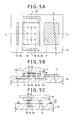
- FIG. 5A is a plan view showing a process of manufacturing the semiconductor device according to the present embodiment.
- FIG. 5B and FIG. 5C are schematic sectional views taken along lines X-X′ and Y-Y′, respectively, of FIG. 5A .
- a breaking point is produced in a surface oxide film by press contact below a solder melting point, and after heating to a solder melting temperature, the solders are connected to each other by oscillation operation in an X-direction and a Y-direction, so that the bumps 21 and the bumps 33 are integrated into bumps 24 .
- the bump 23 and the bumps 35 are integrated into a dam 25 in the region for forming the dam.
- a dam is formed on the two sides.
- a dam is formed on the side or the plurality of sides.
- the bump 23 and the bumps 35 to form the dam may each be formed at the same time as or separately from the bumps 21 of the first semiconductor chip 10 and the bumps 33 of the second semiconductor chip 30 .
- FIG. 6A is a plan view showing a process of manufacturing the semiconductor device according to the present embodiment.
- FIG. 6B and FIG. 6C are schematic sectional views taken along lines X-X′ and Y-Y′, respectively, of FIG. 6A .
- An underfill resin layer 26 is formed so as to be filled into the gap between the first semiconductor chip 10 and the second semiconductor chip 30 , the protrusion of the underfill resin layer 26 from the outer edge of the second semiconductor chip 30 to the side of the electronic circuit section such as the solid-state imaging section 11 , the pad electrode 12 and the like being prevented by the dam 25 .
- a resin in a liquid form which resin is to form the underfill resin layer is injected into the gap between the first semiconductor chip 10 and the second semiconductor chip 30 .
- a resin injection port and an air outlet port are desirably formed to secure a passage for an air to escape from the gap between the first semiconductor chip 10 and the second semiconductor chip 30 .
- the electronic circuit section is provided in each of parts adjacent to two opposed sides of the second semiconductor chip.
- One of sides other than the above sides is an injection port for the resin, and the other side is an air outlet port.
- thermosetting process is performed after the underfill resin layer 26 is formed by the resin in the gap between the first semiconductor chip 10 and the second semiconductor chip 30 as described above.
- thermosetting process a reactant gas is emitted from the fillet of the underfill resin layer 26 .
- the above-described dam 25 prevents the protrusion of the underfill resin layer 26 from the outer edge of the second semiconductor chip 30 to the side of the electronic circuit section.
- a distance of 200 ⁇ m or more can be secured between the fillet of the underfill resin layer 26 and the electronic circuit section such as the solid-state imaging device, the pad electrode and the like.
- the second semiconductor chip and the electronic circuit section such as the pad electrode, the solid-state imaging device or the like can be brought into proximity to each other, and thus the semiconductor device can be miniaturized.
- FIG. 7A is a plan view of a semiconductor device according to a present embodiment.
- FIG. 7B and FIG. 7C are schematic sectional views taken along lines X-X′ and Y-Y′, respectively, of FIG. 7A .
- the fillet of an underfill resin layer 26 is not formed in a region of the periphery of a laminated second semiconductor chip in which region a dam 25 prevents the protrusion of the underfill resin layer 26 from the outer edge of the second semiconductor chip 30 to the side of an electronic circuit section.
- the present embodiment has a layout such that the electronic circuit section such as a pad electrode, a solid-state imaging section and the like and the second semiconductor chip are adjacent to each other in the region in which the dam 25 is formed. Being adjacent in this case indicates that a distance between the electronic circuit section and the second semiconductor chip is zero or in the vicinity of zero.
- the second embodiment has a similar constitution to that of the first embodiment.
- a dam is formed on all sides facing the electronic circuit section.
- a sufficient distance of 200 ⁇ m or more can be secured as a distance between the fillet and the electronic circuit section even in a part where the fillet and the electronic circuit section are closest to each other.
- the second semiconductor chip and the electronic circuit section such as the pad electrode, the solid-state imaging device or the like can be brought into proximity to each other, and thus the semiconductor device can be miniaturized.
- FIG. 8A is a plan view of a semiconductor device according to a present embodiment.
- FIG. 8B and FIG. 8C are schematic sectional views taken along lines X-X′ and Y-Y′, respectively, of FIG. 8A .
- a dam is formed in a shape along the outer edge of a second semiconductor chip.
- a recess-shaped part 27 is formed in a ring-shaped bump 23 on the side of a first semiconductor chip 10 which bump 23 forms a dam in a part in which a solid-state imaging section 11 is laid out close to the region of the second semiconductor chip 30 .
- the third embodiment has a similar constitution to that of the first embodiment.
- an underfill resin layer 26 has a fillet 26 a at a peripheral part of the second semiconductor chip 30 on which peripheral part the dam 25 is not formed.
- dam 25 prevents the protrusion of the underfill resin layer 26 from the outer edge of the second semiconductor chip 30 to the side of the electronic circuit section.
- a sufficient distance of 200 ⁇ m or more can be secured as a distance between the fillet of the underfill resin layer 26 and the electronic circuit section such as the solid-state imaging device, the pad electrode and the like.
- the second semiconductor chip and the electronic circuit section such as the pad electrode, the solid-state imaging device or the like can be brought into proximity to each other, and thus the semiconductor device can be miniaturized.
- FIG. 9A and FIG. 9B are sectional views showing a process of manufacturing a semiconductor device according to a present embodiment, and are schematic sectional views corresponding to the lines X-X′ and Y-Y′ in the semiconductor device shown in FIGS. 1A to 1C .
- a film-shaped underfill resin layer 26 f may be formed on a second semiconductor chip 30 , and the filling of a resin serving as the underfill resin layer may be performed at the same time as the bump connection of a first semiconductor chip 10 .
- a film-shaped underfill resin layer 26 f may be formed on the first semiconductor chip 10 , and the filling of a resin serving as the underfill resin layer may be performed at the same time as the bump connection of the second semiconductor chip 30 .
- the film-shaped underfill resin layer 26 f is subjected to pressure to fill the gap between the first semiconductor chip 10 and the second semiconductor chip 30 , and a surplus is discharged to the outside of the gap. It is therefore important to provide, in advance, a part serving as a resin outlet port from which the surplus can be discharged.
- an electronic circuit section is provided in each of parts adjacent to two opposed sides of the second semiconductor chip.
- the regions of two sides other than the above sides are a resin outlet port.
- the fourth embodiment has a similar constitution to that of the first embodiment.
- the above-described dam 25 prevents the protrusion of the underfill resin layer 26 from the outer edge of the second semiconductor chip 30 to the side of the electronic circuit section.
- a distance of 200 ⁇ m or more can be secured between the fillet of the underfill resin layer 26 and the electronic circuit section such as a solid-state imaging device, a pad electrode and the like.
- the second semiconductor chip and the electronic circuit section such as the pad electrode, the solid-state imaging section or the like can be brought into proximity to each other, and thus the semiconductor device can be miniaturized.
- FIG. 10A is a plan view of a semiconductor device according to a present embodiment.
- FIG. 10B and FIG. 10C are schematic sectional views taken along lines X-X′ and Y-Y′, respectively, of FIG. 10A .
- a dam for preventing the protrusion of an underfill resin layer 26 from the outer edge of a second semiconductor chip 30 to the side of an electronic circuit section may be a resin material.
- a concrete example of the resin material is a photosensitive curing resin or a thermosetting resin such as an epoxy resin, an acrylic resin or the like.
- a resin layer 23 r is formed in place of the under bump film 22 and the bump 23 on the side of a first semiconductor chip 10 .
- a resin layer 35 r is formed in place of the under bump film 34 and the bumps 35 on the side of the second semiconductor chip 30 .
- a dam 25 r made of resin is formed with the above-described resin layer 23 r and the resin layer 35 r adhering to each other on a peripheral part of the second semiconductor chip 30 on the side of the electronic circuit section.
- the fifth embodiment has a similar constitution to that of the first embodiment.
- the underfill resin layer 26 has a fillet 26 a at a peripheral part of the second semiconductor chip 30 on which peripheral part the dam 25 r is not formed.
- dam 25 r prevents the protrusion of the underfill resin layer 26 from the outer edge of the second semiconductor chip 30 to the side of the electronic circuit section.
- a sufficient distance of 200 ⁇ m or more can be secured as a distance between the fillet of the underfill resin layer 26 and the electronic circuit section such as a solid-state imaging device, a pad electrode and the like.
- the second semiconductor chip and the electronic circuit section such as the pad electrode, the solid-state imaging section or the like can be brought into proximity to each other, and thus the semiconductor device can be miniaturized.
- FIG. 11A and FIG. 11B are sectional views showing a process of manufacturing a semiconductor device according to a present embodiment, and are schematic sectional views corresponding to the lines X-X′ and Y-Y′ in the semiconductor device shown in FIGS. 10A to 10C .
- a resin layer 23 r is pattern-formed in place of the under bump film 22 and the bump 23 on the side of a first semiconductor chip 10 .
- a resin layer 35 r is pattern-formed in place of the under bump film 34 and the bumps 35 on the side of a second semiconductor chip 30 .
- a method for pattern-forming the resin can be carried out by forming a resin material into a film by film lamination, spin coating or the like and performing a photolithography process or the like.
- a photosensitive curing resin or a thermosetting resin such as an epoxy resin or an acrylic resin, for example, can be used as the resin layer 23 r and the resin layer 35 r.
- a dam 25 r made of resin is formed with the resin layer 23 r and the resin layer 35 r adhering to each other on a peripheral part of the second semiconductor chip 30 on the side of the electronic circuit section.
- Heating at the time of bump connection or separate curing is performed for adhesion between the resin layer 23 r and the first semiconductor chip 10 , between the resin layer 35 r and the second semiconductor chip 30 , and between the resin layer 23 r and the resin layer 35 r.
- the fifth embodiment has a similar constitution to that of the first embodiment.
- the above-described dam 25 r prevents the protrusion of the underfill resin layer 26 from the outer edge of the second semiconductor chip 30 to the side of the electronic circuit section.
- a distance of 200 ⁇ m or more can be secured between the fillet of the underfill resin layer 26 and the electronic circuit section such as a solid-state imaging section, a pad electrode and the like.
- the second semiconductor chip and the electronic circuit section such as the pad electrode, the solid-state imaging section or the like can be brought into proximity to each other, and thus the semiconductor device can be miniaturized.
- FIG. 12 is a schematic block diagram of an electronic device as an electronic device according to a present embodiment.
- the electronic device according to the present embodiment is an example of a video electronic device capable of photographing a still image or photographing a moving image.
- the electronic device has an image sensor (semiconductor device having a solid-state imaging element section) 50 , an optical system 51 , a signal processing circuit 53 , and the like.
- the semiconductor device having the solid-state imaging element section according to each of the foregoing embodiments is incorporated as the above-described image sensor 50 .
- the optical system 51 forms an image of image light (incident light) from a subject onto the image pickup surface of the image sensor 50 .
- image light incident light
- a corresponding signal charge is accumulated within the image sensor 50 in a certain period.
- the accumulated signal charge is extracted as an output signal Vout.
- a shutter device controls a period of irradiation of the image sensor 50 with light and a period of shielding the image sensor 50 from light.
- the image processing section supplies a driving signal for controlling the transfer operation of the image sensor 50 and the shutter operation of the shutter device.
- the signal transfer of the image sensor 50 is performed according to the driving signal (timing signal) supplied from the image processing section.
- the signal processing circuit 53 subjects the output signal Vout of the image sensor 50 to various signal processing, and then outputs the result as a video signal.
- the video signal resulting from the signal processing is stored on a storage medium such as a memory or the like, or output to a monitor.
- the present invention is not limited to application to solid-state imaging element sections for sensing a distribution of amounts of incident visible light and picking up the distribution as an image, the solid-state imaging element sections being provided in semiconductor devices.
- the present invention is applicable to solid-state imaging sections for picking up a distribution of amounts of incidence of infrared rays, X-rays, or particles or the like as an image and, in a broad sense, solid-state imaging sections in general such as fingerprint detecting sensors and the like for sensing a distribution of another physical quantity such as pressure, capacitance or the like, and picking up the distribution as an image.
- the present invention is applicable to for example digital still electronic devices, video electronic devices, and electronic devices having an imaging function such as portable telephones.
- the image sensor 50 described above can be used as a semiconductor device having a solid-state imaging element section, which is an electronic device module or the like for video electronic devices and digital still electronic devices as well as mobile devices such as portable telephones.
- the present invention is not limited to the above description.
- the embodiment of the present invention is applicable to various sensors such as a CMOS (Complementary Metal Oxide Semiconductor) image sensor and a CCD (Charge Coupled Device) image sensor as the solid-state imaging section.
- CMOS Complementary Metal Oxide Semiconductor
- CCD Charge Coupled Device
Abstract
Disclosed herein is a semiconductor device including: a first semiconductor chip having an electronic circuit section and a first connecting section formed on one surface thereof; a second semiconductor chip having a second connecting section formed on one surface thereof, the second semiconductor chip being mounted on the first semiconductor chip with the first and the second connecting sections connected to each other by a bump; a dam formed to fill a gap between the first and the second semiconductor chips on a part of an outer edge of the second semiconductor chip, the part of the outer edge being on a side of a region of formation of the electronic circuit section; and an underfill resin layer filled into the gap, protrusion of the resin layer from the outer edge of the second semiconductor chip to a side of the electronic circuit section being prevented by the dam.
Description
This application is a continuation of U.S. patent application Ser. No. 15/010,992, filed Jan. 29, 2016, now U.S. Pat. No. 9,691,805, which is a continuation of U.S. patent application Ser. No. 14/297,779, filed Jun. 6, 2014, now U.S. Pat. No. 9,275,922, which is a continuation of U.S. patent application Ser. No. 13/086,830, filed Apr. 14, 2011, now U.S. Pat. No. 8,773,583, which claims priority to Japanese Patent Application No. JP 2010-111910, filed in the Japan Patent Office on May 14, 2010, the entire disclosures of which are hereby incorporated herein by reference.
The present invention relates to a semiconductor device, a method for manufacturing the same, and an electronic device, and particularly to a semiconductor device packaged by mounting a second semiconductor chip on a first semiconductor chip having an electronic circuit section such as a solid-state imaging element section or the like, a method for manufacturing the same, and an electronic device having the same.
A package structure referred to as a chip-on-chip (CoC) package, which includes a plurality of semiconductor chips laminated and sealed within the single package to achieve miniaturization, high functionality and the like of a semiconductor device, has been put to practical use.
The CoC package is also applied to for example a structure in which a memory element and a processor element are laminated, and progress has been made in practical use of the CoC package as a SIP (System in Package) type semiconductor device.
For example, when an SIP is formed by a CoC package as in Japanese Patent Laid-Open No. 2008-192815 (hereinafter referred to as Patent Document 1), the application of flip chip connection is principally considered for connection between an upper semiconductor chip and a lower semiconductor chip.
In the case where flip chip connection is applied to connection between semiconductor chips in a CoC package, a first semiconductor chip (lower stage side semiconductor chip) is mounted on a wiring board having an external connection terminal and the like.
A second semiconductor chip (upper stage side semiconductor chip) is flip-chip-connected to the first semiconductor chip.
That is, electrical and mechanical connection between the first and second semiconductor chips is made by connecting a bump electrode provided on the upper surface of the first semiconductor chip and a bump electrode provided on the lower surface of the second semiconductor chip to each other.
Further, an underfill resin layer is filled into a gap between the first and second semiconductor chips to improve connection reliability and the like.
Japanese Patent Laid-Open Nos. 2005-276879, 2008-252027 and 2008-124140 (hereinafter referred to as Patent Document 2, 3 and 4, respectively), for example, disclose techniques for forming a dam that serves to stop the flow of the underfill resin layer in the case of the structure in which the gap between the first and second semiconductor chips of the CoC package is filled with the underfill resin layer.
The dam is intended mainly to prevent resin contamination caused by a flow of the underfill resin layer into an electronic circuit section such as an Al electrode formed in the first semiconductor chip in a peripheral part of a mounting region of the second semiconductor chip.
In the CoC package of the above-described constitution, a reactant gas is emitted from a fillet of the underfill resin layer, which fillet is formed at the peripheral part of the second semiconductor chip, at a time of resin curing reaction.
In Patent Documents 1 to 4, when a distance between the electronic circuit section such as the Al electrode and the like and the upper semiconductor chip is shortened to miniaturize the CoC package, the above-described gas contaminates the electronic circuit section such as the Al electrode and the like.
As a result, a failure in wire bonding and a degradation in reliability occur, and it is therefore difficult to miniaturize the CoC package.
In addition, in a case where a solid-state imaging element section is formed on the lower semiconductor chip, even when a dam is formed between the solid-state imaging element section and the upper semiconductor chip, the imaging element section is contaminated by the reactant gas emitted from the fillet of the above-described underfill resin layer, and thus an imaging characteristic is degraded.
In addition, a semiconductor device in which rewiring is formed on a glass substrate or the like and a semiconductor chip having a solid-state imaging section formed thereon is flip-chip-connected is under study.
In order to prevent a resin protecting a bump electrode from contaminating the light receiving surface of the solid-state imaging section, techniques for forming a dam between the bump electrode and the semiconductor chip having the solid-state imaging section formed thereon are under study.
However, reference to Japanese Patent Laid-Open Nos. 2007-533131, 2002-118207 and Hei 06-204442 (hereinafter referred Patent Document 5, 6 and 7, respectively) and the like shows that a dam made of a resin is formed on only the side of the glass substrate, and that there is a problem in a sealing property for the side of the semiconductor chip having the solid-state imaging section formed thereon.
In addition, this technique can essentially form a bump electrode only in a peripheral part of a laminated semiconductor chip or the semiconductor chip having a solid-state imaging section formed thereon.
Further, in semiconductor devices disclosed in Patent Documents 6 and 7, no dam is formed on the side of an Al electrode, and there is thus a fear of contamination of the Al electrode.
A problem to be solved is that when the distance between the electronic circuit section formed on the lower semiconductor chip and the upper semiconductor chip is shortened, the electronic circuit section is contaminated by the reactant gas emitted from the fillet of the underfill resin layer between the upper semiconductor chip and the lower semiconductor chip.
It is thus difficult to achieve miniaturization and a higher degree of integration of the semiconductor device by shortening the distance between the upper semiconductor chip and the electronic circuit section formed on the lower semiconductor chip.
According to an embodiment of the present invention, there is provided a semiconductor device including: a first semiconductor chip having an electronic circuit section formed at least on one surface of the first semiconductor chip, and having a first connecting section formed on a same surface as the surface of formation of the electronic circuit section; a second semiconductor chip having a second connecting section formed on one surface of the second semiconductor chip, the second semiconductor chip being mounted on the first semiconductor chip with the first connecting section and the second connecting section connected to each other by a bump; a dam formed so as to fill a gap between the first semiconductor chip and the second semiconductor chip on at least a part of an outer edge of the second semiconductor chip, the part of the outer edge of the second semiconductor chip being on a side of a region of formation of the electronic circuit section; and an underfill resin layer filled into the gap between the first semiconductor chip and the second semiconductor chip, protrusion of the underfill resin layer from the outer edge of the second semiconductor chip to a side of the electronic circuit section being prevented by the dam.
In the semiconductor device according to the above-described embodiment of the present invention, a second semiconductor chip having a second connecting section formed on one surface of the second semiconductor chip is mounted on a first semiconductor chip having an electronic circuit section formed at least on one surface of the first semiconductor chip, and having a first connecting section formed on a same surface as the surface of formation of the electronic circuit section, with the first semiconductor chip and the second semiconductor chip connected to each other at the first connecting section and the second connecting section by a bump.
In this case, a dam for filling a gap between the first semiconductor chip and the second semiconductor chip is formed on at least a part of an outer edge of the second semiconductor chip, the part of the outer edge of the second semiconductor chip being on a side of a region of formation of the electronic circuit section.
An underfill resin layer is filled into the gap between the first semiconductor chip and the second semiconductor chip, protrusion of the underfill resin layer from the outer edge of the second semiconductor chip to a side of the electronic circuit section being prevented by the dam.
In addition, according to an embodiment of the present invention, there is provided a method for manufacturing a semiconductor device, the method including the steps of: forming an electronic circuit section at least on one surface of a first semiconductor chip, and forming a first connecting section on a same surface as the surface of formation of the electronic circuit section; forming a second connecting section on one surface of a second semiconductor chip; mounting the second semiconductor chip on the first semiconductor chip with the first connecting section and the second connecting section connected to each other by a bump; forming a dam for filling a gap between the first semiconductor chip and the second semiconductor chip on at least a part of an outer edge of the second semiconductor chip, the part of the outer edge of the second semiconductor chip being on a side of a region of formation of the electronic circuit section; and forming an underfill resin layer so as to fill the underfill resin layer into the gap between the first semiconductor chip and the second semiconductor chip, protrusion of the underfill resin layer from the outer edge of the second semiconductor chip to a side of the electronic circuit section being prevented by the dam.
In the method for manufacturing the semiconductor device according to the above-described embodiment of the present invention, an electronic circuit section is formed at least on one surface of a first semiconductor chip, and a first connecting section is formed on a same surface as the surface of formation of the electronic circuit section.
In addition, a second connecting section is formed on one surface of a second semiconductor chip.
Next, the second semiconductor chip is mounted on the first semiconductor chip with the first connecting section and the second connecting section connected to each other by a bump.
In the above, a dam for filling a gap between the first semiconductor chip and the second semiconductor chip is formed on at least a part of an outer edge of the second semiconductor chip, the part of the outer edge of the second semiconductor chip being on a side of a region of formation of the electronic circuit section.
Next, an underfill resin layer is formed so as to be filled into the gap between the first semiconductor chip and the second semiconductor chip, protrusion of the underfill resin layer from the outer edge of the second semiconductor chip to a side of the electronic circuit section being prevented by the dam.
According to an embodiment of the present invention, there is provided an electronic device including: a solid-state imaging device; an optical system for guiding incident light to an imaging section of the solid-state imaging device; and a signal processing circuit for processing an output signal of the solid-state imaging device; wherein the solid-state imaging device includes a first semiconductor chip having a solid-state imaging section formed at least on one surface of the first semiconductor chip, and having a first connecting section formed on a same surface as the surface of formation of the solid-state imaging section, a second semiconductor chip having a second connecting section formed on one surface of the second semiconductor chip, the second semiconductor chip being mounted on the first semiconductor chip with the first connecting section and the second connecting section connected to each other by a bump, a dam formed so as to fill a gap between the first semiconductor chip and the second semiconductor chip on at least a part of an outer edge of the second semiconductor chip, the part of the outer edge of the second semiconductor chip being on a side of a region of formation of the solid-state imaging section, and an underfill resin layer filled into the gap between the first semiconductor chip and the second semiconductor chip, protrusion of the underfill resin layer from the outer edge of the second semiconductor chip to a side of the solid-state imaging section being prevented by the dam.
The electronic device according to the above-described embodiment of the present invention includes: a solid-state imaging device; an optical system for guiding incident light to an imaging section of the solid-state imaging device; and a signal processing circuit for processing an output signal of the solid-state imaging device.
In the solid-state imaging device, a second semiconductor chip having a second connecting section formed on one surface of the second semiconductor chip is mounted on a first semiconductor chip having a solid-state imaging section formed at least on one surface of the first semiconductor chip, and having a first connecting section formed on a same surface as the surface of formation of the solid-state imaging section, with the first semiconductor chip and the second semiconductor chip connected to each other at the first connecting section and the second connecting section by a bump. In addition, a dam for filling a gap between the first semiconductor chip and the second semiconductor chip is formed on at least a part of an outer edge of the second semiconductor chip, the part of the outer edge of the second semiconductor chip being on a side of a region of formation of the solid-state imaging section. Further, an underfill resin layer is filled into the gap between the first semiconductor chip and the second semiconductor chip, protrusion of the underfill resin layer from the outer edge of the second semiconductor chip to a side of the solid-state imaging section being prevented by the dam.
In the semiconductor device according to the above-described embodiment of the present invention, the dam prevents the protrusion of the underfill resin layer between the first and second semiconductor chips from the outer edge of the second semiconductor chip to the side of the electronic circuit section. Thus, the fillet of the underfill resin layer is not formed in the vicinity of the electronic circuit section, and the contamination of the electronic circuit section by a reactant gas emitted from the fillet is prevented.
Thus, it is possible to shorten the distance between the electronic circuit section formed on the first semiconductor chip and the second semiconductor chip, and thus achieve miniaturization and a higher degree of integration of the semiconductor device.
The method for manufacturing the semiconductor device according to the above-described embodiment of the present invention forms the dam to prevent the protrusion of the underfill resin layer between the first and second semiconductor chips from the outer edge of the second semiconductor chip to the side of the electronic circuit section. Thus, the fillet of the underfill resin layer is not formed in the vicinity of the electronic circuit section, and the contamination of the electronic circuit section by a reactant gas emitted from the fillet can be prevented.
Thus, it is possible to shorten the distance between the electronic circuit section formed on the first semiconductor chip and the second semiconductor chip, and thus achieve miniaturization and a higher degree of integration of the semiconductor device.
In the solid-state imaging device forming the electronic device according to the above-described embodiment of the present invention, the dam prevents the protrusion of the underfill resin layer between the first and second semiconductor chips from the outer edge of the second semiconductor chip to the side of the solid-state imaging section. Thus, the fillet of the underfill resin layer is not formed in the vicinity of the solid-state imaging section, and the contamination of the solid-state imaging section by a reactant gas emitted from the fillet is prevented.
Thus, it is possible to shorten the distance between the solid-state imaging section formed on the first semiconductor chip and the second semiconductor chip, and thus achieve miniaturization and a higher degree of integration of the solid-state imaging device.
Preferred embodiments of a solid-state imaging device, a method for manufacturing the same, a designing method, and an electronic device according to the present invention will hereinafter be described with reference to the drawings.
Incidentally, description will be made in the following order.
1. First Embodiment (Basic Constitution of Semiconductor Device and Manufacturing Method)
2. Second Embodiment (Constitution in which Electronic Circuit Section and Second Semiconductor Chip are Formed so as to be Adjacent to Each Other)
3. Third Embodiment (Constitution in which Dam is Formed in Shape along Outer Edge of Second Semiconductor Chip)
4. Fourth Embodiment (Manufacturing Method Using Resin Film as Underfill Resin Layer)
5. Fifth Embodiment (Constitution in which Dam is Formed by Resin)
6. Sixth Embodiment (Application to Electronic Device)
[Constitution of Semiconductor Device]
An electronic circuit section is formed at least on one surface of a first semiconductor chip 10.
A solid-state imaging section 11, for example, is formed as the electronic circuit section described above.
In the solid-state imaging section 11, for example, photodiodes are formed so as to be divided from each other for each pixel, and pixels including photodiodes are arranged in the form of a matrix to form a light receiving surface. For example, an insulating film, a color filter, an on-chip lens and the like are formed on the light receiving surface as required.
In addition, a pad electrode 12, for example, is formed as the electronic circuit section.
The pad electrode 12 is formed of aluminum, for example. The pad electrode 12 is buried in the vicinity of a top layer of the first semiconductor chip 10. A part of the pad electrode 12 is exposed on the top surface side by a pad opening part 12 a.
In addition, other peripheral circuit sections such for example as a comparator and a DA converter may be included as the electronic circuit section.
For example, internal wiring 13 connected to the solid-state imaging section 11, the pad electrode 12 and the like is formed so as to be buried within the first semiconductor chip 10.
An under bump film 20 as a first connecting section is formed on the same surface of the first semiconductor chip 10 as the surface of the first semiconductor chip 10 on which surface the electronic circuit section is formed.
On the other hand, wiring 31 and the like are formed on a second semiconductor chip 30, and an under bump film 32 as a second connecting section is formed on one surface of the second semiconductor chip 30.
The second semiconductor chip 30 is mounted on the first semiconductor chip 10, the first semiconductor chip 10 and the second semiconductor chip 30 being connected to each other at the under bump film 20 and the under bump film 32 by bumps 24.
In this case, a dam 25 for filling a gap between the first semiconductor chip 10 and the second semiconductor chip 30 is formed on at least a part of an outer edge of the second semiconductor chip 30 which part is on the side of a region in which the electronic circuit section is formed.
In addition, in the present embodiment, an under bump film 22 is formed on the side of the first semiconductor chip 10, and an under bump film 34 is formed on the side of the second semiconductor chip 30. The above-described dam 25 is formed so as to connect the under bump film 22 and the under bump film 34 to each other. The dam 25 is formed by the same layer as a conductive layer forming the bumps 24. Bumps 23 are formed on the first semiconductor chip 10 in regions other than a region formed such that the gap between the first semiconductor chip 10 and the second semiconductor chip 30 is filled. The dam 25 and the bumps 23 together form a ring shape.
The gap between the first semiconductor chip 10 and the second semiconductor chip 30 is filled with an underfill resin layer 26, the protrusion of the underfill resin layer 26 from the outer edge of the second semiconductor chip 30 to the side of the electronic circuit section being prevented by the dam 25.
In the semiconductor device according to the present embodiment, the underfill resin layer 26 has a fillet 26 a at a peripheral part of the second semiconductor chip 30 on which peripheral part the dam 25 is not formed.
However, the above-described dam 25 prevents the protrusion of the underfill resin layer 26 from the outer edge of the second semiconductor chip 30 to the side of the electronic circuit section.
For example, in order to prevent contamination from a reactant gas from the fillet, it is important to secure a distance of 200 μm or more between the fillet and the electronic circuit section.
In the present embodiment, a distance of 200 μm or more can be secured between the fillet of the underfill resin layer 26 and the electronic circuit section such as the solid-state imaging device, the pad electrode and the like.
Therefore, the contamination of the electronic circuit section by a reactant gas emitted at a time of resin curing reaction from the fillet of the underfill resin layer 26 can be prevented.
In the above-described embodiment, a constitution having the solid-state imaging device and the pad electrode as the electronic circuit section has been shown. However, the embodiment is applicable to a case where one of the solid-state imaging device and the pad electrode or an electronic circuit section whose contamination by another reactant gas is desirably avoided is present.
As described above, in the present embodiment, when the electronic circuit section is provided in each of parts adjacent to two opposed sides of the second semiconductor chip, a dam is formed on the two sides. When the electronic circuit section is provided on another side or a plurality of sides, it suffices to form a dam on the side or the plurality of sides.
A material for forming the dam 25 may be formed by a same layer as the bumps formed on the first or second semiconductor chip, or may be a different layer. For example, a metal such as Cu, An, Ti or the like or a soldering material such as Sn, SnAg, SnAgCu, SnCu, AuSn or the like can be used.
Thus, the second semiconductor chip and the electronic circuit section such as the pad electrode, the solid-state imaging device or the like can be brought into proximity to each other, and thus the semiconductor device can be miniaturized.
[Method for Manufacturing Semiconductor Device]
A method for manufacturing the semiconductor device according to the present embodiment will next be described with reference to FIGS. 2A to 6C .
An electronic circuit section is formed at least on one surface of the first semiconductor chip 10. A solid-state imaging section 11, for example, is formed as the above-described electronic circuit section.
In the solid-state imaging section 11, for example, photodiodes are formed so as to be divided from each other for each pixel, and pixels including photodiodes are arranged in the form of a matrix to form a light receiving surface. For example, an insulating film, a color filter, an on-chip lens and the like are formed on the light receiving surface as required.
In addition, a pad electrode 12, for example, is formed as the electronic circuit section.
The pad electrode 12 is formed of aluminum, for example. The pad electrode 12 is formed so as to be buried in the vicinity of a top layer of the first semiconductor chip 10. A pad opening part 12 a is formed so as to expose a part of the pad electrode 12.
In addition, other peripheral circuit sections such for example as a comparator and a DA converter may be included as the electronic circuit section.
In addition, for example, internal wiring 13 connected to the solid-state imaging section 11, the pad electrode 12 and the like is formed so as to be buried within the first semiconductor chip 10.
An under bump film 20 as a first connecting section is formed on the same surface of the first semiconductor chip 10 as the surface of the first semiconductor chip 10 on which surface the electronic circuit section is formed.
In addition, an under bump film 22 of a ring shape is formed on a peripheral part of a region for mounting a second semiconductor chip including a region for forming a dam.
The bump 23 is formed in a ring shape on the peripheral part of the region for mounting the second semiconductor chip as described above.
In addition, an under bump film 34 of a linear shape is formed on two sides of an outer edge of the second semiconductor chip, the two sides being a region for forming the dam.
The bumps 35 are formed in a linear shape on the two sides of the outer edge of the second semiconductor chip as described above.
Using a collet 40 or the like as appropriate, the bumps 21 and the bump 23 of the first semiconductor chip 10 described above are aligned with the bumps 33 and the bumps 35 of the second semiconductor chip 30, and the second semiconductor chip 30 is mounted on the first semiconductor chip 10.
Using a bonding head 41 or the like as appropriate, a breaking point is produced in a surface oxide film by press contact below a solder melting point, and after heating to a solder melting temperature, the solders are connected to each other by oscillation operation in an X-direction and a Y-direction, so that the bumps 21 and the bumps 33 are integrated into bumps 24.
At the same time as the above, the bump 23 and the bumps 35 are integrated into a dam 25 in the region for forming the dam.
As described above, in the present embodiment, when the electronic circuit section is provided in each of parts adjacent to two opposed sides of the second semiconductor chip, a dam is formed on the two sides. When the electronic circuit section is provided on another side or a plurality of sides, a dam is formed on the side or the plurality of sides.
In addition, no problem is presented even when a flux is applied in advance in connecting the bumps made of solder. Incidentally, the bump 23 and the bumps 35 to form the dam may each be formed at the same time as or separately from the bumps 21 of the first semiconductor chip 10 and the bumps 33 of the second semiconductor chip 30.
An underfill resin layer 26 is formed so as to be filled into the gap between the first semiconductor chip 10 and the second semiconductor chip 30, the protrusion of the underfill resin layer 26 from the outer edge of the second semiconductor chip 30 to the side of the electronic circuit section such as the solid-state imaging section 11, the pad electrode 12 and the like being prevented by the dam 25.
Using a dispenser 26 d, for example, a resin in a liquid form which resin is to form the underfill resin layer is injected into the gap between the first semiconductor chip 10 and the second semiconductor chip 30.
In filling the above-described resin, a resin injection port and an air outlet port, for example, are desirably formed to secure a passage for an air to escape from the gap between the first semiconductor chip 10 and the second semiconductor chip 30.
As described above, in the present embodiment, the electronic circuit section is provided in each of parts adjacent to two opposed sides of the second semiconductor chip. One of sides other than the above sides is an injection port for the resin, and the other side is an air outlet port.
A thermosetting process is performed after the underfill resin layer 26 is formed by the resin in the gap between the first semiconductor chip 10 and the second semiconductor chip 30 as described above.
In the above thermosetting process, a reactant gas is emitted from the fillet of the underfill resin layer 26.
In the method for manufacturing the semiconductor device according to the present embodiment, the above-described dam 25 prevents the protrusion of the underfill resin layer 26 from the outer edge of the second semiconductor chip 30 to the side of the electronic circuit section.
A distance of 200 μm or more can be secured between the fillet of the underfill resin layer 26 and the electronic circuit section such as the solid-state imaging device, the pad electrode and the like.
Therefore, the contamination of the electronic circuit section by the reactant gas emitted at a time of resin curing reaction from the fillet of the underfill resin layer 26 can be prevented.
Thus, in the method for manufacturing the semiconductor device according to the present embodiment, the second semiconductor chip and the electronic circuit section such as the pad electrode, the solid-state imaging device or the like can be brought into proximity to each other, and thus the semiconductor device can be miniaturized.
[Constitution of Semiconductor Device]
The fillet of an underfill resin layer 26 is not formed in a region of the periphery of a laminated second semiconductor chip in which region a dam 25 prevents the protrusion of the underfill resin layer 26 from the outer edge of the second semiconductor chip 30 to the side of an electronic circuit section.
The present embodiment has a layout such that the electronic circuit section such as a pad electrode, a solid-state imaging section and the like and the second semiconductor chip are adjacent to each other in the region in which the dam 25 is formed. Being adjacent in this case indicates that a distance between the electronic circuit section and the second semiconductor chip is zero or in the vicinity of zero.
Except for the above, the second embodiment has a similar constitution to that of the first embodiment.
While a fillet is formed in a region in which the above-described dam 25 is not formed, a dam is formed on all sides facing the electronic circuit section. Thus, a sufficient distance of 200 μm or more can be secured as a distance between the fillet and the electronic circuit section even in a part where the fillet and the electronic circuit section are closest to each other.
Therefore, the contamination of the electronic circuit section by a reactant gas emitted at a time of resin curing reaction from the fillet of the underfill resin layer 26 can be prevented.
Thus, the second semiconductor chip and the electronic circuit section such as the pad electrode, the solid-state imaging device or the like can be brought into proximity to each other, and thus the semiconductor device can be miniaturized.
[Constitution of Semiconductor Device]
A dam is formed in a shape along the outer edge of a second semiconductor chip. Specifically, in the present embodiment, a recess-shaped part 27 is formed in a ring-shaped bump 23 on the side of a first semiconductor chip 10 which bump 23 forms a dam in a part in which a solid-state imaging section 11 is laid out close to the region of the second semiconductor chip 30.
When an electronic circuit section such as a pad electrode 12, the solid-state imaging section 11 and the like is present in the vicinity of the second semiconductor chip 30, and the length of the electronic circuit section is shorter than the length of the side wall of the second semiconductor chip 30, it suffices to form a dam only in a part close to the electronic circuit section.
Except for the above, the third embodiment has a similar constitution to that of the first embodiment.
In the semiconductor device according to the present embodiment, an underfill resin layer 26 has a fillet 26 a at a peripheral part of the second semiconductor chip 30 on which peripheral part the dam 25 is not formed.
However, the above-described dam 25 prevents the protrusion of the underfill resin layer 26 from the outer edge of the second semiconductor chip 30 to the side of the electronic circuit section.
In the present embodiment, a sufficient distance of 200 μm or more can be secured as a distance between the fillet of the underfill resin layer 26 and the electronic circuit section such as the solid-state imaging device, the pad electrode and the like.
Therefore, the contamination of the electronic circuit section by a reactant gas emitted at a time of resin curing reaction from the fillet of the underfill resin layer 26 can be prevented.
Thus, the second semiconductor chip and the electronic circuit section such as the pad electrode, the solid-state imaging device or the like can be brought into proximity to each other, and thus the semiconductor device can be miniaturized.
As described above, the foregoing effects can be obtained even when the dam formation region is only in the vicinity of the electronic circuit section.
[Method for Manufacturing Semiconductor Device]
When an underfill resin layer is formed, a film-shaped underfill resin layer 26 f may be formed on a second semiconductor chip 30, and the filling of a resin serving as the underfill resin layer may be performed at the same time as the bump connection of a first semiconductor chip 10.
Alternatively, a film-shaped underfill resin layer 26 f may be formed on the first semiconductor chip 10, and the filling of a resin serving as the underfill resin layer may be performed at the same time as the bump connection of the second semiconductor chip 30.
As shown in FIG. 9A and FIG. 9B , the film-shaped underfill resin layer 26 f is subjected to pressure to fill the gap between the first semiconductor chip 10 and the second semiconductor chip 30, and a surplus is discharged to the outside of the gap. It is therefore important to provide, in advance, a part serving as a resin outlet port from which the surplus can be discharged.
As described above, in the present embodiment, an electronic circuit section is provided in each of parts adjacent to two opposed sides of the second semiconductor chip. The regions of two sides other than the above sides are a resin outlet port.
Except for the above, the fourth embodiment has a similar constitution to that of the first embodiment.
In the method for manufacturing the semiconductor device according to the present embodiment, the above-described dam 25 prevents the protrusion of the underfill resin layer 26 from the outer edge of the second semiconductor chip 30 to the side of the electronic circuit section.
A distance of 200 μm or more can be secured between the fillet of the underfill resin layer 26 and the electronic circuit section such as a solid-state imaging device, a pad electrode and the like.
Therefore, the contamination of the electronic circuit section by a reactant gas emitted at a time of resin curing reaction from the fillet of the underfill resin layer 26 can be prevented.
Thus, in the method for manufacturing the semiconductor device according to the present embodiment, the second semiconductor chip and the electronic circuit section such as the pad electrode, the solid-state imaging section or the like can be brought into proximity to each other, and thus the semiconductor device can be miniaturized.
[Constitution of Semiconductor Device]
A dam for preventing the protrusion of an underfill resin layer 26 from the outer edge of a second semiconductor chip 30 to the side of an electronic circuit section may be a resin material. A concrete example of the resin material is a photosensitive curing resin or a thermosetting resin such as an epoxy resin, an acrylic resin or the like.
Specifically, in the present embodiment, a resin layer 23 r is formed in place of the under bump film 22 and the bump 23 on the side of a first semiconductor chip 10.
A resin layer 35 r is formed in place of the under bump film 34 and the bumps 35 on the side of the second semiconductor chip 30.
Further, a dam 25 r made of resin is formed with the above-described resin layer 23 r and the resin layer 35 r adhering to each other on a peripheral part of the second semiconductor chip 30 on the side of the electronic circuit section.
Except for the above, the fifth embodiment has a similar constitution to that of the first embodiment.
In the semiconductor device according to the present embodiment, the underfill resin layer 26 has a fillet 26 a at a peripheral part of the second semiconductor chip 30 on which peripheral part the dam 25 r is not formed.
However, the above-described dam 25 r prevents the protrusion of the underfill resin layer 26 from the outer edge of the second semiconductor chip 30 to the side of the electronic circuit section.
In the present embodiment, a sufficient distance of 200 μm or more can be secured as a distance between the fillet of the underfill resin layer 26 and the electronic circuit section such as a solid-state imaging device, a pad electrode and the like.
Therefore, the contamination of the electronic circuit section by a reactant gas emitted at a time of resin curing reaction from the fillet of the underfill resin layer 26 can be prevented.
Thus, the second semiconductor chip and the electronic circuit section such as the pad electrode, the solid-state imaging section or the like can be brought into proximity to each other, and thus the semiconductor device can be miniaturized.
[Method for Manufacturing Semiconductor Device]
In the present embodiment, a resin layer 23 r is pattern-formed in place of the under bump film 22 and the bump 23 on the side of a first semiconductor chip 10.
In addition, a resin layer 35 r is pattern-formed in place of the under bump film 34 and the bumps 35 on the side of a second semiconductor chip 30.
A method for pattern-forming the resin can be carried out by forming a resin material into a film by film lamination, spin coating or the like and performing a photolithography process or the like.
A photosensitive curing resin or a thermosetting resin such as an epoxy resin or an acrylic resin, for example, can be used as the resin layer 23 r and the resin layer 35 r.
Next, a dam 25 r made of resin is formed with the resin layer 23 r and the resin layer 35 r adhering to each other on a peripheral part of the second semiconductor chip 30 on the side of the electronic circuit section.
Heating at the time of bump connection or separate curing is performed for adhesion between the resin layer 23 r and the first semiconductor chip 10, between the resin layer 35 r and the second semiconductor chip 30, and between the resin layer 23 r and the resin layer 35 r.
Except for the above, the fifth embodiment has a similar constitution to that of the first embodiment.
In the method for manufacturing the semiconductor device according to the present embodiment, the above-described dam 25 r prevents the protrusion of the underfill resin layer 26 from the outer edge of the second semiconductor chip 30 to the side of the electronic circuit section.
A distance of 200 μm or more can be secured between the fillet of the underfill resin layer 26 and the electronic circuit section such as a solid-state imaging section, a pad electrode and the like.
Therefore, the contamination of the electronic circuit section by a reactant gas emitted at a time of resin curing reaction from the fillet of the underfill resin layer 26 can be prevented.
Thus, in the method for manufacturing the semiconductor device according to the present embodiment, the second semiconductor chip and the electronic circuit section such as the pad electrode, the solid-state imaging section or the like can be brought into proximity to each other, and thus the semiconductor device can be miniaturized.
[Application to Electronic Device]
The electronic device according to the present embodiment has an image sensor (semiconductor device having a solid-state imaging element section) 50, an optical system 51, a signal processing circuit 53, and the like.
In the present embodiment, the semiconductor device having the solid-state imaging element section according to each of the foregoing embodiments is incorporated as the above-described image sensor 50.
The optical system 51 forms an image of image light (incident light) from a subject onto the image pickup surface of the image sensor 50. Thus, a corresponding signal charge is accumulated within the image sensor 50 in a certain period. The accumulated signal charge is extracted as an output signal Vout.
A shutter device controls a period of irradiation of the image sensor 50 with light and a period of shielding the image sensor 50 from light.
The image processing section supplies a driving signal for controlling the transfer operation of the image sensor 50 and the shutter operation of the shutter device. The signal transfer of the image sensor 50 is performed according to the driving signal (timing signal) supplied from the image processing section. The signal processing circuit 53 subjects the output signal Vout of the image sensor 50 to various signal processing, and then outputs the result as a video signal. The video signal resulting from the signal processing is stored on a storage medium such as a memory or the like, or output to a monitor.
In addition, the present invention is not limited to application to solid-state imaging element sections for sensing a distribution of amounts of incident visible light and picking up the distribution as an image, the solid-state imaging element sections being provided in semiconductor devices.
The present invention is applicable to solid-state imaging sections for picking up a distribution of amounts of incidence of infrared rays, X-rays, or particles or the like as an image and, in a broad sense, solid-state imaging sections in general such as fingerprint detecting sensors and the like for sensing a distribution of another physical quantity such as pressure, capacitance or the like, and picking up the distribution as an image.
In addition, the present invention is applicable to for example digital still electronic devices, video electronic devices, and electronic devices having an imaging function such as portable telephones.
The image sensor 50 described above can be used as a semiconductor device having a solid-state imaging element section, which is an electronic device module or the like for video electronic devices and digital still electronic devices as well as mobile devices such as portable telephones.
The present invention is not limited to the above description.
For example, while a pad electrode and a solid-state imaging section have been described as an electronic circuit section, an embodiment of the present invention is applicable to other electronic circuit sections.
The embodiment of the present invention is applicable to various sensors such as a CMOS (Complementary Metal Oxide Semiconductor) image sensor and a CCD (Charge Coupled Device) image sensor as the solid-state imaging section.
In addition, various changes can be made without departing from the spirit of the present invention.
It should be understood by those skilled in the art that various modifications, combinations, sub-combinations and alterations may occur depending on design requirements and other factor in so far as they are within the scope of the appended claims or the equivalents thereof.
Claims (17)
1. An imaging device comprising:
a first substrate including a first connection section and an electronic circuit section including a plurality of pixels;
a pad electrode within the first substrate;
a pad opening in the first substrate exposing a portion of the pad electrode;
a second substrate including a second connection section, the second substrate being mounted on the first substrate with the first connection section and the second connection section connected to each other by a connecting member, wherein the connecting member is between the first substrate and the second substrate on at least a part of an outer edge of the second substrate;
at least one bump electrically connecting the first substrate to the second substrate; and
a filling layer formed between the first substrate and the second substrate, wherein the filling layer includes a protrusion from at least one outer edge of the second substrate, and wherein a region including the connecting member and the filling layer is between a region including the pad opening and a region including the at least one bump.
2. The imaging device according to claim 1 , wherein the filling layer is an underfill resin layer.
3. The imaging device according to claim 1 , further including an internal wiring within the first substrate electrically connecting the pad electrode and the at least one bump.
4. The imaging device according to claim 1 , wherein a second region including the connecting member and the filling layer is between a second bump that is electrically connected to the electronic circuit section including the plurality of pixels.
5. The imaging device according to claim 4 , further including an internal wiring within the first substrate electrically connecting the second bump to the electronic circuit section.
6. The imaging device according to claim 1 , wherein the connecting member is between the first substrate and the second substrate on at least a part of the outer edge of the second substrate being at a side of a region of formation of the pad electrode.
7. The imaging device according to claim 6 , wherein the filling layer includes a second protrusion from another outer edge of the second substrate.
8. An electronic device comprising:
an imaging device;
an optical system for guiding incident light to an imaging section of the imaging device; and
a signal processing circuit for processing an output signal of the imaging device,
wherein the imaging device includes:
a first substrate including a first connection section and an electronic circuit section including a plurality of pixels,
a pad electrode within the first substrate,
a pad opening in the first substrate exposing a portion of the pad electrode,
a second substrate including a second connection section, the second substrate being mounted on the first substrate with the first connection section and the second connection section connected to each other by a connecting member, wherein the connecting member is between the first substrate and the second substrate on at least a part of an outer edge of the second substrate,
at least one bump electrically connecting the first substrate to the second substrate, and
a filling layer formed between the first substrate and the second substrate, wherein the filling layer includes a protrusion from at least one outer edge of the second substrate, and wherein a region including the connecting member and the filling layer is between a region including the pad opening and a region including the at least one bump.
9. The electronic device according to claim 8 , wherein the filling layer is an underfill resin layer.
10. The electronic device according to claim 8 , further including an internal wiring within the first substrate electrically connecting the pad electrode and the at least one bump.
11. The electronic device according to claim 8 , wherein a second region including the connecting member and the filling layer is between a second bump that is electrically connected to the electronic circuit section including the plurality of pixels.
12. The electronic device according to claim 8 , wherein the connecting member is between the first substrate and the second substrate on at least a part of the outer edge of the second substrate being at a side of a region of formation of the pad electrode.
13. A method of manufacturing an imaging device, the method comprising:
forming a first connection section on a first substrate, the first substrate including an electronic circuit section including a plurality of pixels;
forming a second connection section on a second substrate;
forming at least one bump on the first substrate and/or the second substrate;
mounting the second substrate to the first substrate such that a connecting member is between the first substrate and the second substrate on at least a part of an outer edge of the second substrate; and
forming a filling layer between the first substrate and the second substrate, wherein the filling layer includes a protrusion from at least one outer edge of the second substrate, and wherein a region including the connecting member and the filling layer is between a region including a pad opening and a region including the at least one bump.
14. The method of manufacturing according to claim 13 , wherein the filling layer is an underfill resin layer.
15. The method of manufacturing according to claim 13 , further including an internal wiring within the first substrate electrically connecting a pad electrode and the at least one bump.
16. The method of manufacturing according to claim 15 , wherein a second region including the connecting member and the filling layer is between a second bump that is electrically connected to the electronic circuit section including the plurality of pixels.
17. The method of manufacturing according to claim 13 , wherein the connecting member is between the first substrate and the second substrate on at least a part of the outer edge of the second substrate being at a side of a region of formation of a pad electrode.
Priority Applications (1)
| Application Number | Priority Date | Filing Date | Title |
|---|---|---|---|
| US15/630,783 US10026770B2 (en) | 2010-05-14 | 2017-06-22 | Semiconductor device, method for manufacturing the same, and electronic device |
Applications Claiming Priority (6)
| Application Number | Priority Date | Filing Date | Title |
|---|---|---|---|
| JP2010111910A JP2011243612A (en) | 2010-05-14 | 2010-05-14 | Semiconductor device and its manufacturing method and electronic apparatus |
| JP2010-111910 | 2010-05-14 | ||
| US13/086,830 US8773583B2 (en) | 2010-05-14 | 2011-04-14 | Semiconductor device, method for manufacturing the same, and electronic device |
| US14/297,779 US9275922B2 (en) | 2010-05-14 | 2014-06-06 | Semiconductor device, method for manufacturing the same, and electronic device |
| US15/010,992 US9691805B2 (en) | 2010-05-14 | 2016-01-29 | Semiconductor device, method for manufacturing the same, and electronic device |
| US15/630,783 US10026770B2 (en) | 2010-05-14 | 2017-06-22 | Semiconductor device, method for manufacturing the same, and electronic device |
Related Parent Applications (1)
| Application Number | Title | Priority Date | Filing Date |
|---|---|---|---|
| US15/010,992 Continuation US9691805B2 (en) | 2010-05-14 | 2016-01-29 | Semiconductor device, method for manufacturing the same, and electronic device |
Publications (2)
| Publication Number | Publication Date |
|---|---|
| US20170287968A1 US20170287968A1 (en) | 2017-10-05 |
| US10026770B2 true US10026770B2 (en) | 2018-07-17 |
Family
ID=44911483
Family Applications (4)
| Application Number | Title | Priority Date | Filing Date |
|---|---|---|---|
| US13/086,830 Expired - Fee Related US8773583B2 (en) | 2010-05-14 | 2011-04-14 | Semiconductor device, method for manufacturing the same, and electronic device |
| US14/297,779 Expired - Fee Related US9275922B2 (en) | 2010-05-14 | 2014-06-06 | Semiconductor device, method for manufacturing the same, and electronic device |
| US15/010,992 Active US9691805B2 (en) | 2010-05-14 | 2016-01-29 | Semiconductor device, method for manufacturing the same, and electronic device |
| US15/630,783 Expired - Fee Related US10026770B2 (en) | 2010-05-14 | 2017-06-22 | Semiconductor device, method for manufacturing the same, and electronic device |
Family Applications Before (3)
| Application Number | Title | Priority Date | Filing Date |
|---|---|---|---|
| US13/086,830 Expired - Fee Related US8773583B2 (en) | 2010-05-14 | 2011-04-14 | Semiconductor device, method for manufacturing the same, and electronic device |
| US14/297,779 Expired - Fee Related US9275922B2 (en) | 2010-05-14 | 2014-06-06 | Semiconductor device, method for manufacturing the same, and electronic device |
| US15/010,992 Active US9691805B2 (en) | 2010-05-14 | 2016-01-29 | Semiconductor device, method for manufacturing the same, and electronic device |
Country Status (5)
| Country | Link |
|---|---|
| US (4) | US8773583B2 (en) |
| JP (1) | JP2011243612A (en) |
| KR (2) | KR20110126040A (en) |
| CN (1) | CN102244068B (en) |
| TW (1) | TWI499025B (en) |
Families Citing this family (20)
| Publication number | Priority date | Publication date | Assignee | Title |
|---|---|---|---|---|
| CN104737290B (en) * | 2012-10-26 | 2017-09-19 | 奥林巴斯株式会社 | Solid camera head, camera device and signal reading method |
| JP2016027586A (en) * | 2012-11-29 | 2016-02-18 | パナソニック株式会社 | Optical device and manufacturing method for optical device |
| WO2014083750A1 (en) * | 2012-11-30 | 2014-06-05 | パナソニック株式会社 | Optical apparatus and method for manufacturing same |
| JP5799973B2 (en) * | 2013-04-15 | 2015-10-28 | 株式会社村田製作所 | Ceramic multilayer wiring board and module including the same |
| US9368458B2 (en) * | 2013-07-10 | 2016-06-14 | Taiwan Semiconductor Manufacturing Company, Ltd. | Die-on-interposer assembly with dam structure and method of manufacturing the same |
| JP6120075B2 (en) * | 2013-07-19 | 2017-04-26 | ソニー株式会社 | Solid-state imaging device and manufacturing method of solid-state imaging device. |
| WO2015056430A1 (en) * | 2013-10-16 | 2015-04-23 | パナソニック株式会社 | Semiconductor device |
| US10020236B2 (en) * | 2014-03-14 | 2018-07-10 | Taiwan Semiconductar Manufacturing Campany | Dam for three-dimensional integrated circuit |
| TWI669810B (en) * | 2014-09-11 | 2019-08-21 | 日商索尼半導體解決方案公司 | Solid-state imaging device, imaging device, electronic device, and semiconductor device |
| CN104505393A (en) * | 2014-09-16 | 2015-04-08 | 华天科技(昆山)电子有限公司 | Back-illuminated image sensor three-dimensional stacked packaging structure and packaging technology |
| US9508660B2 (en) * | 2015-02-10 | 2016-11-29 | Intel Corporation | Microelectronic die having chamfered corners |
| JP6432737B2 (en) | 2015-03-04 | 2018-12-05 | セイコーエプソン株式会社 | MEMS device, head, and liquid ejecting apparatus |
| JP6295983B2 (en) | 2015-03-05 | 2018-03-20 | ソニー株式会社 | SEMICONDUCTOR DEVICE, ITS MANUFACTURING METHOD, AND ELECTRONIC DEVICE |
| JP6693068B2 (en) * | 2015-03-12 | 2020-05-13 | ソニー株式会社 | Solid-state imaging device, manufacturing method, and electronic device |
| CN107025481B (en) * | 2016-02-02 | 2021-08-20 | 上海伯乐电子有限公司 | Flexible printed circuit board, smart card module using same and smart card |
| WO2018074581A1 (en) * | 2016-10-21 | 2018-04-26 | ソニーセミコンダクタソリューションズ株式会社 | Electronic substrate and electronic device |
| US11676929B2 (en) | 2016-10-21 | 2023-06-13 | Sony Semiconductor Solutions Corporation | Electronic substrate and electronic apparatus |
| JP7236807B2 (en) * | 2018-01-25 | 2023-03-10 | 浜松ホトニクス株式会社 | Semiconductor device and method for manufacturing semiconductor device |
| JP7353121B2 (en) * | 2019-10-08 | 2023-09-29 | キヤノン株式会社 | Semiconductor devices and equipment |
| US11862550B2 (en) | 2021-09-30 | 2024-01-02 | Advanced Semiconductor Engineering, Inc. | Electronic package structure and method of manufacturing the same |
Citations (7)
| Publication number | Priority date | Publication date | Assignee | Title |
|---|---|---|---|---|
| US20040263668A1 (en) * | 2003-06-18 | 2004-12-30 | Dong-Han Kim | Solid-state imaging method and apparatus |
| US20060023109A1 (en) * | 2004-07-30 | 2006-02-02 | Sony Corporation | Semiconductor module, MOS type solid-state image pickup device, camera and manufacturing method of camera |
| US20070007667A1 (en) * | 2004-04-12 | 2007-01-11 | Deok-Hoon Kim | Electronic package having a sealing structure on predetermined area, and the method thereof |
| US20080093722A1 (en) * | 2006-10-19 | 2008-04-24 | Norihiko Shishido | Encapsulation type semiconductor device and manufacturing method thereof |
| US20080237892A1 (en) * | 2007-03-30 | 2008-10-02 | Oki Electric Industry Co., Ltd. | Semiconductor device |
| US20090008765A1 (en) * | 2005-12-14 | 2009-01-08 | Takaharu Yamano | Chip embedded substrate and method of producing the same |
| US20100244173A1 (en) * | 2009-03-30 | 2010-09-30 | Taiwan Semiconductor Manufacturing Company, Ltd. | Image sensor and method of fabricating same |
Family Cites Families (14)
| Publication number | Priority date | Publication date | Assignee | Title |
|---|---|---|---|---|
| JP2522039B2 (en) * | 1989-04-12 | 1996-08-07 | 日本電気株式会社 | Film carrier type semiconductor device |
| JPH06204442A (en) | 1993-01-07 | 1994-07-22 | Matsushita Electron Corp | Slid-state image sensing apparatus and manufacture thereof |
| JP3367272B2 (en) * | 1994-05-16 | 2003-01-14 | 株式会社日立製作所 | Lead frame and semiconductor device |
| KR100343432B1 (en) | 2000-07-24 | 2002-07-11 | 한신혁 | Semiconductor package and package method |
| JP3544970B2 (en) * | 2002-09-30 | 2004-07-21 | 沖電気工業株式会社 | COF tape carrier, semiconductor element, semiconductor device |
| JP2004228106A (en) * | 2003-01-20 | 2004-08-12 | Nec Kansai Ltd | Semiconductor device |
| JP2005116628A (en) * | 2003-10-03 | 2005-04-28 | Matsushita Electric Ind Co Ltd | Solid-state imaging device and manufacturing method thereof |
| JP4415717B2 (en) | 2004-03-23 | 2010-02-17 | ソニー株式会社 | Semiconductor device and manufacturing method thereof |
| JP4489611B2 (en) * | 2005-02-02 | 2010-06-23 | 京セラケミカル株式会社 | Optical electronics |
| JP5331303B2 (en) | 2006-11-09 | 2013-10-30 | ルネサスエレクトロニクス株式会社 | Manufacturing method of semiconductor device |
| JP2008124161A (en) * | 2006-11-10 | 2008-05-29 | Misuzu Kogyo:Kk | Electronic apparatus housing package and method of manufacturing electronic apparatus housing package |
| JP4435187B2 (en) | 2007-02-05 | 2010-03-17 | 株式会社東芝 | Multilayer semiconductor device |
| TW200941677A (en) * | 2008-03-27 | 2009-10-01 | Phoenix Prec Technology Corp | Package substrate and fabrication method thereof |
| KR20100108109A (en) * | 2009-03-27 | 2010-10-06 | 삼성전자주식회사 | Image sensor and fabricating method thereof |
-
2010
- 2010-05-14 JP JP2010111910A patent/JP2011243612A/en active Pending
-
2011
- 2011-04-13 TW TW100112831A patent/TWI499025B/en not_active IP Right Cessation
- 2011-04-14 US US13/086,830 patent/US8773583B2/en not_active Expired - Fee Related
- 2011-05-02 KR KR1020110041377A patent/KR20110126040A/en not_active Application Discontinuation
- 2011-05-06 CN CN201110117484.4A patent/CN102244068B/en not_active Expired - Fee Related
-
2014
- 2014-06-06 US US14/297,779 patent/US9275922B2/en not_active Expired - Fee Related
-
2016
- 2016-01-29 US US15/010,992 patent/US9691805B2/en active Active
-
2017
- 2017-06-22 US US15/630,783 patent/US10026770B2/en not_active Expired - Fee Related
-
2018
- 2018-02-28 KR KR1020180024291A patent/KR101902731B1/en active IP Right Grant
Patent Citations (7)
| Publication number | Priority date | Publication date | Assignee | Title |
|---|---|---|---|---|
| US20040263668A1 (en) * | 2003-06-18 | 2004-12-30 | Dong-Han Kim | Solid-state imaging method and apparatus |
| US20070007667A1 (en) * | 2004-04-12 | 2007-01-11 | Deok-Hoon Kim | Electronic package having a sealing structure on predetermined area, and the method thereof |
| US20060023109A1 (en) * | 2004-07-30 | 2006-02-02 | Sony Corporation | Semiconductor module, MOS type solid-state image pickup device, camera and manufacturing method of camera |
| US20090008765A1 (en) * | 2005-12-14 | 2009-01-08 | Takaharu Yamano | Chip embedded substrate and method of producing the same |
| US20080093722A1 (en) * | 2006-10-19 | 2008-04-24 | Norihiko Shishido | Encapsulation type semiconductor device and manufacturing method thereof |
| US20080237892A1 (en) * | 2007-03-30 | 2008-10-02 | Oki Electric Industry Co., Ltd. | Semiconductor device |
| US20100244173A1 (en) * | 2009-03-30 | 2010-09-30 | Taiwan Semiconductor Manufacturing Company, Ltd. | Image sensor and method of fabricating same |
Also Published As
| Publication number | Publication date |
|---|---|
| US8773583B2 (en) | 2014-07-08 |
| JP2011243612A (en) | 2011-12-01 |
| CN102244068A (en) | 2011-11-16 |
| US20170287968A1 (en) | 2017-10-05 |
| US20110279717A1 (en) | 2011-11-17 |
| US9275922B2 (en) | 2016-03-01 |
| TWI499025B (en) | 2015-09-01 |
| CN102244068B (en) | 2015-07-22 |
| TW201201343A (en) | 2012-01-01 |
| KR20180029209A (en) | 2018-03-20 |
| US20140284749A1 (en) | 2014-09-25 |
| US9691805B2 (en) | 2017-06-27 |
| US20160163756A1 (en) | 2016-06-09 |
| KR20110126040A (en) | 2011-11-22 |
| KR101902731B1 (en) | 2018-09-28 |
Similar Documents
| Publication | Publication Date | Title |
|---|---|---|
| US10026770B2 (en) | Semiconductor device, method for manufacturing the same, and electronic device | |
| US8012776B2 (en) | Methods of manufacturing imaging device packages | |
| US7701044B2 (en) | Chip package for image sensor and method of manufacturing the same | |
| US11043436B2 (en) | Semiconductor device, manufacturing method, imaging device, and electronic apparatus for enabling component mounting with high flatness | |
| US7202460B2 (en) | Camera module for compact electronic equipments | |
| JP3877860B2 (en) | Semiconductor device with solid-state image sensor and method for manufacturing the semiconductor device | |
| US20130264703A1 (en) | Semiconductor packages and methods for manufacturing the same | |
| US20130292786A1 (en) | Integrated optical sensor module | |
| US20240038796A1 (en) | Solid-state imaging device and electronic device | |
| US20060180888A1 (en) | Optical sensor package and method of manufacture | |
| US20040234190A1 (en) | Optical modules and method for manufacturing the same, and electronic devices | |
| US20040065933A1 (en) | Flip chip optical and imaging sensor device | |
| KR20050116760A (en) | Package for image sensor | |
| US20090315130A1 (en) | Solid-state imaging apparatus and method for manufacturing the same | |
| JP2007027452A (en) | Solid-state image sensing device module and method of manufacturing the same |
Legal Events
| Date | Code | Title | Description |
|---|---|---|---|
| STCF | Information on status: patent grant |
Free format text: PATENTED CASE |
|
| FEPP | Fee payment procedure |
Free format text: MAINTENANCE FEE REMINDER MAILED (ORIGINAL EVENT CODE: REM.); ENTITY STATUS OF PATENT OWNER: LARGE ENTITY |
|
| LAPS | Lapse for failure to pay maintenance fees |
Free format text: PATENT EXPIRED FOR FAILURE TO PAY MAINTENANCE FEES (ORIGINAL EVENT CODE: EXP.); ENTITY STATUS OF PATENT OWNER: LARGE ENTITY |
|
| STCH | Information on status: patent discontinuation |
Free format text: PATENT EXPIRED DUE TO NONPAYMENT OF MAINTENANCE FEES UNDER 37 CFR 1.362 |
|
| FP | Lapsed due to failure to pay maintenance fee |
Effective date: 20220717 |