TWI759064B - Seal device and forming method of the device - Google Patents
Seal device and forming method of the device Download PDFInfo
- Publication number
- TWI759064B TWI759064B TW110100939A TW110100939A TWI759064B TW I759064 B TWI759064 B TW I759064B TW 110100939 A TW110100939 A TW 110100939A TW 110100939 A TW110100939 A TW 110100939A TW I759064 B TWI759064 B TW I759064B
- Authority
- TW
- Taiwan
- Prior art keywords
- sealing
- contact
- compressible
- circuit
- sealing member
- Prior art date
Links
Images


Classifications
-
- H—ELECTRICITY
- H01—ELECTRIC ELEMENTS
- H01L—SEMICONDUCTOR DEVICES NOT COVERED BY CLASS H10
- H01L21/00—Processes or apparatus adapted for the manufacture or treatment of semiconductor or solid state devices or of parts thereof
- H01L21/02—Manufacture or treatment of semiconductor devices or of parts thereof
- H01L21/04—Manufacture or treatment of semiconductor devices or of parts thereof the devices having at least one potential-jump barrier or surface barrier, e.g. PN junction, depletion layer or carrier concentration layer
- H01L21/50—Assembly of semiconductor devices using processes or apparatus not provided for in a single one of the subgroups H01L21/06 - H01L21/326, e.g. sealing of a cap to a base of a container
- H01L21/52—Mounting semiconductor bodies in containers
-
- H—ELECTRICITY
- H01—ELECTRIC ELEMENTS
- H01L—SEMICONDUCTOR DEVICES NOT COVERED BY CLASS H10
- H01L21/00—Processes or apparatus adapted for the manufacture or treatment of semiconductor or solid state devices or of parts thereof
- H01L21/67—Apparatus specially adapted for handling semiconductor or electric solid state devices during manufacture or treatment thereof; Apparatus specially adapted for handling wafers during manufacture or treatment of semiconductor or electric solid state devices or components ; Apparatus not specifically provided for elsewhere
- H01L21/67005—Apparatus not specifically provided for elsewhere
- H01L21/67011—Apparatus for manufacture or treatment
- H01L21/67098—Apparatus for thermal treatment
- H01L21/67103—Apparatus for thermal treatment mainly by conduction
-
- H—ELECTRICITY
- H01—ELECTRIC ELEMENTS
- H01L—SEMICONDUCTOR DEVICES NOT COVERED BY CLASS H10
- H01L23/00—Details of semiconductor or other solid state devices
- H01L23/28—Encapsulations, e.g. encapsulating layers, coatings, e.g. for protection
- H01L23/31—Encapsulations, e.g. encapsulating layers, coatings, e.g. for protection characterised by the arrangement or shape
- H01L23/3107—Encapsulations, e.g. encapsulating layers, coatings, e.g. for protection characterised by the arrangement or shape the device being completely enclosed
- H01L23/3114—Encapsulations, e.g. encapsulating layers, coatings, e.g. for protection characterised by the arrangement or shape the device being completely enclosed the device being a chip scale package, e.g. CSP
-
- A—HUMAN NECESSITIES
- A61—MEDICAL OR VETERINARY SCIENCE; HYGIENE
- A61B—DIAGNOSIS; SURGERY; IDENTIFICATION
- A61B5/00—Measuring for diagnostic purposes; Identification of persons
- A61B5/02—Detecting, measuring or recording pulse, heart rate, blood pressure or blood flow; Combined pulse/heart-rate/blood pressure determination; Evaluating a cardiovascular condition not otherwise provided for, e.g. using combinations of techniques provided for in this group with electrocardiography or electroauscultation; Heart catheters for measuring blood pressure
- A61B5/024—Detecting, measuring or recording pulse rate or heart rate
-
- B—PERFORMING OPERATIONS; TRANSPORTING
- B29—WORKING OF PLASTICS; WORKING OF SUBSTANCES IN A PLASTIC STATE IN GENERAL
- B29C—SHAPING OR JOINING OF PLASTICS; SHAPING OF MATERIAL IN A PLASTIC STATE, NOT OTHERWISE PROVIDED FOR; AFTER-TREATMENT OF THE SHAPED PRODUCTS, e.g. REPAIRING
- B29C65/00—Joining or sealing of preformed parts, e.g. welding of plastics materials; Apparatus therefor
- B29C65/02—Joining or sealing of preformed parts, e.g. welding of plastics materials; Apparatus therefor by heating, with or without pressure
- B29C65/18—Joining or sealing of preformed parts, e.g. welding of plastics materials; Apparatus therefor by heating, with or without pressure using heated tools
- B29C65/20—Joining or sealing of preformed parts, e.g. welding of plastics materials; Apparatus therefor by heating, with or without pressure using heated tools with direct contact, e.g. using "mirror"
-
- H—ELECTRICITY
- H01—ELECTRIC ELEMENTS
- H01L—SEMICONDUCTOR DEVICES NOT COVERED BY CLASS H10
- H01L21/00—Processes or apparatus adapted for the manufacture or treatment of semiconductor or solid state devices or of parts thereof
- H01L21/02—Manufacture or treatment of semiconductor devices or of parts thereof
- H01L21/04—Manufacture or treatment of semiconductor devices or of parts thereof the devices having at least one potential-jump barrier or surface barrier, e.g. PN junction, depletion layer or carrier concentration layer
- H01L21/48—Manufacture or treatment of parts, e.g. containers, prior to assembly of the devices, using processes not provided for in a single one of the subgroups H01L21/06 - H01L21/326
- H01L21/4814—Conductive parts
-
- H—ELECTRICITY
- H01—ELECTRIC ELEMENTS
- H01L—SEMICONDUCTOR DEVICES NOT COVERED BY CLASS H10
- H01L21/00—Processes or apparatus adapted for the manufacture or treatment of semiconductor or solid state devices or of parts thereof
- H01L21/02—Manufacture or treatment of semiconductor devices or of parts thereof
- H01L21/04—Manufacture or treatment of semiconductor devices or of parts thereof the devices having at least one potential-jump barrier or surface barrier, e.g. PN junction, depletion layer or carrier concentration layer
- H01L21/50—Assembly of semiconductor devices using processes or apparatus not provided for in a single one of the subgroups H01L21/06 - H01L21/326, e.g. sealing of a cap to a base of a container
- H01L21/56—Encapsulations, e.g. encapsulation layers, coatings
-
- H—ELECTRICITY
- H01—ELECTRIC ELEMENTS
- H01L—SEMICONDUCTOR DEVICES NOT COVERED BY CLASS H10
- H01L21/00—Processes or apparatus adapted for the manufacture or treatment of semiconductor or solid state devices or of parts thereof
- H01L21/67—Apparatus specially adapted for handling semiconductor or electric solid state devices during manufacture or treatment thereof; Apparatus specially adapted for handling wafers during manufacture or treatment of semiconductor or electric solid state devices or components ; Apparatus not specifically provided for elsewhere
- H01L21/67005—Apparatus not specifically provided for elsewhere
- H01L21/67011—Apparatus for manufacture or treatment
- H01L21/67126—Apparatus for sealing, encapsulating, glassing, decapsulating or the like
-
- H—ELECTRICITY
- H01—ELECTRIC ELEMENTS
- H01L—SEMICONDUCTOR DEVICES NOT COVERED BY CLASS H10
- H01L23/00—Details of semiconductor or other solid state devices
- H01L23/02—Containers; Seals
- H01L23/04—Containers; Seals characterised by the shape of the container or parts, e.g. caps, walls
-
- H—ELECTRICITY
- H01—ELECTRIC ELEMENTS
- H01L—SEMICONDUCTOR DEVICES NOT COVERED BY CLASS H10
- H01L23/00—Details of semiconductor or other solid state devices
- H01L23/02—Containers; Seals
- H01L23/10—Containers; Seals characterised by the material or arrangement of seals between parts, e.g. between cap and base of the container or between leads and walls of the container
-
- H—ELECTRICITY
- H01—ELECTRIC ELEMENTS
- H01L—SEMICONDUCTOR DEVICES NOT COVERED BY CLASS H10
- H01L23/00—Details of semiconductor or other solid state devices
- H01L23/48—Arrangements for conducting electric current to or from the solid state body in operation, e.g. leads, terminal arrangements ; Selection of materials therefor
- H01L23/481—Internal lead connections, e.g. via connections, feedthrough structures
-
- H—ELECTRICITY
- H01—ELECTRIC ELEMENTS
- H01L—SEMICONDUCTOR DEVICES NOT COVERED BY CLASS H10
- H01L24/00—Arrangements for connecting or disconnecting semiconductor or solid-state bodies; Methods or apparatus related thereto
- H01L24/80—Methods for connecting semiconductor or other solid state bodies using means for bonding being attached to, or being formed on, the surface to be connected
- H01L24/81—Methods for connecting semiconductor or other solid state bodies using means for bonding being attached to, or being formed on, the surface to be connected using a bump connector
-
- B—PERFORMING OPERATIONS; TRANSPORTING
- B29—WORKING OF PLASTICS; WORKING OF SUBSTANCES IN A PLASTIC STATE IN GENERAL
- B29C—SHAPING OR JOINING OF PLASTICS; SHAPING OF MATERIAL IN A PLASTIC STATE, NOT OTHERWISE PROVIDED FOR; AFTER-TREATMENT OF THE SHAPED PRODUCTS, e.g. REPAIRING
- B29C65/00—Joining or sealing of preformed parts, e.g. welding of plastics materials; Apparatus therefor
- B29C65/02—Joining or sealing of preformed parts, e.g. welding of plastics materials; Apparatus therefor by heating, with or without pressure
- B29C65/04—Dielectric heating, e.g. high-frequency welding, i.e. radio frequency welding of plastic materials having dielectric properties, e.g. PVC
-
- B—PERFORMING OPERATIONS; TRANSPORTING
- B29—WORKING OF PLASTICS; WORKING OF SUBSTANCES IN A PLASTIC STATE IN GENERAL
- B29C—SHAPING OR JOINING OF PLASTICS; SHAPING OF MATERIAL IN A PLASTIC STATE, NOT OTHERWISE PROVIDED FOR; AFTER-TREATMENT OF THE SHAPED PRODUCTS, e.g. REPAIRING
- B29C65/00—Joining or sealing of preformed parts, e.g. welding of plastics materials; Apparatus therefor
- B29C65/02—Joining or sealing of preformed parts, e.g. welding of plastics materials; Apparatus therefor by heating, with or without pressure
- B29C65/08—Joining or sealing of preformed parts, e.g. welding of plastics materials; Apparatus therefor by heating, with or without pressure using ultrasonic vibrations
-
- B—PERFORMING OPERATIONS; TRANSPORTING
- B29—WORKING OF PLASTICS; WORKING OF SUBSTANCES IN A PLASTIC STATE IN GENERAL
- B29C—SHAPING OR JOINING OF PLASTICS; SHAPING OF MATERIAL IN A PLASTIC STATE, NOT OTHERWISE PROVIDED FOR; AFTER-TREATMENT OF THE SHAPED PRODUCTS, e.g. REPAIRING
- B29C65/00—Joining or sealing of preformed parts, e.g. welding of plastics materials; Apparatus therefor
- B29C65/02—Joining or sealing of preformed parts, e.g. welding of plastics materials; Apparatus therefor by heating, with or without pressure
- B29C65/14—Joining or sealing of preformed parts, e.g. welding of plastics materials; Apparatus therefor by heating, with or without pressure using wave energy, i.e. electromagnetic radiation, or particle radiation
- B29C65/16—Laser beams
-
- B—PERFORMING OPERATIONS; TRANSPORTING
- B29—WORKING OF PLASTICS; WORKING OF SUBSTANCES IN A PLASTIC STATE IN GENERAL
- B29C—SHAPING OR JOINING OF PLASTICS; SHAPING OF MATERIAL IN A PLASTIC STATE, NOT OTHERWISE PROVIDED FOR; AFTER-TREATMENT OF THE SHAPED PRODUCTS, e.g. REPAIRING
- B29C65/00—Joining or sealing of preformed parts, e.g. welding of plastics materials; Apparatus therefor
- B29C65/48—Joining or sealing of preformed parts, e.g. welding of plastics materials; Apparatus therefor using adhesives, i.e. using supplementary joining material; solvent bonding
-
- B—PERFORMING OPERATIONS; TRANSPORTING
- B29—WORKING OF PLASTICS; WORKING OF SUBSTANCES IN A PLASTIC STATE IN GENERAL
- B29C—SHAPING OR JOINING OF PLASTICS; SHAPING OF MATERIAL IN A PLASTIC STATE, NOT OTHERWISE PROVIDED FOR; AFTER-TREATMENT OF THE SHAPED PRODUCTS, e.g. REPAIRING
- B29C66/00—General aspects of processes or apparatus for joining preformed parts
- B29C66/01—General aspects dealing with the joint area or with the area to be joined
- B29C66/05—Particular design of joint configurations
- B29C66/10—Particular design of joint configurations particular design of the joint cross-sections
- B29C66/11—Joint cross-sections comprising a single joint-segment, i.e. one of the parts to be joined comprising a single joint-segment in the joint cross-section
- B29C66/112—Single lapped joints
- B29C66/1122—Single lap to lap joints, i.e. overlap joints
-
- B—PERFORMING OPERATIONS; TRANSPORTING
- B29—WORKING OF PLASTICS; WORKING OF SUBSTANCES IN A PLASTIC STATE IN GENERAL
- B29C—SHAPING OR JOINING OF PLASTICS; SHAPING OF MATERIAL IN A PLASTIC STATE, NOT OTHERWISE PROVIDED FOR; AFTER-TREATMENT OF THE SHAPED PRODUCTS, e.g. REPAIRING
- B29C66/00—General aspects of processes or apparatus for joining preformed parts
- B29C66/01—General aspects dealing with the joint area or with the area to be joined
- B29C66/05—Particular design of joint configurations
- B29C66/20—Particular design of joint configurations particular design of the joint lines, e.g. of the weld lines
- B29C66/24—Particular design of joint configurations particular design of the joint lines, e.g. of the weld lines said joint lines being closed or non-straight
- B29C66/242—Particular design of joint configurations particular design of the joint lines, e.g. of the weld lines said joint lines being closed or non-straight said joint lines being closed, i.e. forming closed contours
- B29C66/2424—Particular design of joint configurations particular design of the joint lines, e.g. of the weld lines said joint lines being closed or non-straight said joint lines being closed, i.e. forming closed contours being a closed polygonal chain
- B29C66/24243—Particular design of joint configurations particular design of the joint lines, e.g. of the weld lines said joint lines being closed or non-straight said joint lines being closed, i.e. forming closed contours being a closed polygonal chain forming a quadrilateral
- B29C66/24244—Particular design of joint configurations particular design of the joint lines, e.g. of the weld lines said joint lines being closed or non-straight said joint lines being closed, i.e. forming closed contours being a closed polygonal chain forming a quadrilateral forming a rectangle
- B29C66/24245—Particular design of joint configurations particular design of the joint lines, e.g. of the weld lines said joint lines being closed or non-straight said joint lines being closed, i.e. forming closed contours being a closed polygonal chain forming a quadrilateral forming a rectangle forming a square
-
- B—PERFORMING OPERATIONS; TRANSPORTING
- B29—WORKING OF PLASTICS; WORKING OF SUBSTANCES IN A PLASTIC STATE IN GENERAL
- B29C—SHAPING OR JOINING OF PLASTICS; SHAPING OF MATERIAL IN A PLASTIC STATE, NOT OTHERWISE PROVIDED FOR; AFTER-TREATMENT OF THE SHAPED PRODUCTS, e.g. REPAIRING
- B29C66/00—General aspects of processes or apparatus for joining preformed parts
- B29C66/40—General aspects of joining substantially flat articles, e.g. plates, sheets or web-like materials; Making flat seams in tubular or hollow articles; Joining single elements to substantially flat surfaces
- B29C66/41—Joining substantially flat articles ; Making flat seams in tubular or hollow articles
- B29C66/43—Joining a relatively small portion of the surface of said articles
- B29C66/433—Casing-in, i.e. enclosing an element between two sheets by an outlined seam
-
- B—PERFORMING OPERATIONS; TRANSPORTING
- B29—WORKING OF PLASTICS; WORKING OF SUBSTANCES IN A PLASTIC STATE IN GENERAL
- B29C—SHAPING OR JOINING OF PLASTICS; SHAPING OF MATERIAL IN A PLASTIC STATE, NOT OTHERWISE PROVIDED FOR; AFTER-TREATMENT OF THE SHAPED PRODUCTS, e.g. REPAIRING
- B29C66/00—General aspects of processes or apparatus for joining preformed parts
- B29C66/70—General aspects of processes or apparatus for joining preformed parts characterised by the composition, physical properties or the structure of the material of the parts to be joined; Joining with non-plastics material
- B29C66/71—General aspects of processes or apparatus for joining preformed parts characterised by the composition, physical properties or the structure of the material of the parts to be joined; Joining with non-plastics material characterised by the composition of the plastics material of the parts to be joined
-
- B—PERFORMING OPERATIONS; TRANSPORTING
- B29—WORKING OF PLASTICS; WORKING OF SUBSTANCES IN A PLASTIC STATE IN GENERAL
- B29C—SHAPING OR JOINING OF PLASTICS; SHAPING OF MATERIAL IN A PLASTIC STATE, NOT OTHERWISE PROVIDED FOR; AFTER-TREATMENT OF THE SHAPED PRODUCTS, e.g. REPAIRING
- B29C66/00—General aspects of processes or apparatus for joining preformed parts
- B29C66/70—General aspects of processes or apparatus for joining preformed parts characterised by the composition, physical properties or the structure of the material of the parts to be joined; Joining with non-plastics material
- B29C66/72—General aspects of processes or apparatus for joining preformed parts characterised by the composition, physical properties or the structure of the material of the parts to be joined; Joining with non-plastics material characterised by the structure of the material of the parts to be joined
- B29C66/723—General aspects of processes or apparatus for joining preformed parts characterised by the composition, physical properties or the structure of the material of the parts to be joined; Joining with non-plastics material characterised by the structure of the material of the parts to be joined being multi-layered
- B29C66/7232—General aspects of processes or apparatus for joining preformed parts characterised by the composition, physical properties or the structure of the material of the parts to be joined; Joining with non-plastics material characterised by the structure of the material of the parts to be joined being multi-layered comprising a non-plastics layer
- B29C66/72321—General aspects of processes or apparatus for joining preformed parts characterised by the composition, physical properties or the structure of the material of the parts to be joined; Joining with non-plastics material characterised by the structure of the material of the parts to be joined being multi-layered comprising a non-plastics layer consisting of metals or their alloys
-
- B—PERFORMING OPERATIONS; TRANSPORTING
- B29—WORKING OF PLASTICS; WORKING OF SUBSTANCES IN A PLASTIC STATE IN GENERAL
- B29C—SHAPING OR JOINING OF PLASTICS; SHAPING OF MATERIAL IN A PLASTIC STATE, NOT OTHERWISE PROVIDED FOR; AFTER-TREATMENT OF THE SHAPED PRODUCTS, e.g. REPAIRING
- B29C66/00—General aspects of processes or apparatus for joining preformed parts
- B29C66/70—General aspects of processes or apparatus for joining preformed parts characterised by the composition, physical properties or the structure of the material of the parts to be joined; Joining with non-plastics material
- B29C66/72—General aspects of processes or apparatus for joining preformed parts characterised by the composition, physical properties or the structure of the material of the parts to be joined; Joining with non-plastics material characterised by the structure of the material of the parts to be joined
- B29C66/723—General aspects of processes or apparatus for joining preformed parts characterised by the composition, physical properties or the structure of the material of the parts to be joined; Joining with non-plastics material characterised by the structure of the material of the parts to be joined being multi-layered
- B29C66/7234—General aspects of processes or apparatus for joining preformed parts characterised by the composition, physical properties or the structure of the material of the parts to be joined; Joining with non-plastics material characterised by the structure of the material of the parts to be joined being multi-layered comprising a barrier layer
- B29C66/72341—General aspects of processes or apparatus for joining preformed parts characterised by the composition, physical properties or the structure of the material of the parts to be joined; Joining with non-plastics material characterised by the structure of the material of the parts to be joined being multi-layered comprising a barrier layer for gases
-
- B—PERFORMING OPERATIONS; TRANSPORTING
- B29—WORKING OF PLASTICS; WORKING OF SUBSTANCES IN A PLASTIC STATE IN GENERAL
- B29C—SHAPING OR JOINING OF PLASTICS; SHAPING OF MATERIAL IN A PLASTIC STATE, NOT OTHERWISE PROVIDED FOR; AFTER-TREATMENT OF THE SHAPED PRODUCTS, e.g. REPAIRING
- B29C66/00—General aspects of processes or apparatus for joining preformed parts
- B29C66/70—General aspects of processes or apparatus for joining preformed parts characterised by the composition, physical properties or the structure of the material of the parts to be joined; Joining with non-plastics material
- B29C66/73—General aspects of processes or apparatus for joining preformed parts characterised by the composition, physical properties or the structure of the material of the parts to be joined; Joining with non-plastics material characterised by the intensive physical properties of the material of the parts to be joined, by the optical properties of the material of the parts to be joined, by the extensive physical properties of the parts to be joined, by the state of the material of the parts to be joined or by the material of the parts to be joined being a thermoplastic or a thermoset
- B29C66/737—General aspects of processes or apparatus for joining preformed parts characterised by the composition, physical properties or the structure of the material of the parts to be joined; Joining with non-plastics material characterised by the intensive physical properties of the material of the parts to be joined, by the optical properties of the material of the parts to be joined, by the extensive physical properties of the parts to be joined, by the state of the material of the parts to be joined or by the material of the parts to be joined being a thermoplastic or a thermoset characterised by the state of the material of the parts to be joined
- B29C66/7371—General aspects of processes or apparatus for joining preformed parts characterised by the composition, physical properties or the structure of the material of the parts to be joined; Joining with non-plastics material characterised by the intensive physical properties of the material of the parts to be joined, by the optical properties of the material of the parts to be joined, by the extensive physical properties of the parts to be joined, by the state of the material of the parts to be joined or by the material of the parts to be joined being a thermoplastic or a thermoset characterised by the state of the material of the parts to be joined oriented or heat-shrinkable
- B29C66/73711—General aspects of processes or apparatus for joining preformed parts characterised by the composition, physical properties or the structure of the material of the parts to be joined; Joining with non-plastics material characterised by the intensive physical properties of the material of the parts to be joined, by the optical properties of the material of the parts to be joined, by the extensive physical properties of the parts to be joined, by the state of the material of the parts to be joined or by the material of the parts to be joined being a thermoplastic or a thermoset characterised by the state of the material of the parts to be joined oriented or heat-shrinkable oriented
- B29C66/73713—General aspects of processes or apparatus for joining preformed parts characterised by the composition, physical properties or the structure of the material of the parts to be joined; Joining with non-plastics material characterised by the intensive physical properties of the material of the parts to be joined, by the optical properties of the material of the parts to be joined, by the extensive physical properties of the parts to be joined, by the state of the material of the parts to be joined or by the material of the parts to be joined being a thermoplastic or a thermoset characterised by the state of the material of the parts to be joined oriented or heat-shrinkable oriented bi-axially or multi-axially
-
- B—PERFORMING OPERATIONS; TRANSPORTING
- B29—WORKING OF PLASTICS; WORKING OF SUBSTANCES IN A PLASTIC STATE IN GENERAL
- B29K—INDEXING SCHEME ASSOCIATED WITH SUBCLASSES B29B, B29C OR B29D, RELATING TO MOULDING MATERIALS OR TO MATERIALS FOR MOULDS, REINFORCEMENTS, FILLERS OR PREFORMED PARTS, e.g. INSERTS
- B29K2705/00—Use of metals, their alloys or their compounds, for preformed parts, e.g. for inserts
- B29K2705/02—Aluminium
-
- B—PERFORMING OPERATIONS; TRANSPORTING
- B29—WORKING OF PLASTICS; WORKING OF SUBSTANCES IN A PLASTIC STATE IN GENERAL
- B29L—INDEXING SCHEME ASSOCIATED WITH SUBCLASS B29C, RELATING TO PARTICULAR ARTICLES
- B29L2031/00—Other particular articles
- B29L2031/34—Electrical apparatus, e.g. sparking plugs or parts thereof
- B29L2031/3425—Printed circuits
-
- H—ELECTRICITY
- H01—ELECTRIC ELEMENTS
- H01L—SEMICONDUCTOR DEVICES NOT COVERED BY CLASS H10
- H01L2224/00—Indexing scheme for arrangements for connecting or disconnecting semiconductor or solid-state bodies and methods related thereto as covered by H01L24/00
- H01L2224/80—Methods for connecting semiconductor or other solid state bodies using means for bonding being attached to, or being formed on, the surface to be connected
- H01L2224/81—Methods for connecting semiconductor or other solid state bodies using means for bonding being attached to, or being formed on, the surface to be connected using a bump connector
Abstract
Description
本發明係關於一種包括被薄膜所密封之電路構件之裝置。 The present invention relates to a device comprising a circuit member encapsulated by a film.
例如在專利文獻1,係開示有一種可薄型化之裝置。 For example, Patent Document 1 discloses a device that can be thinned.
當參照圖19時,於專利文獻1中,係開示有一種半導體晶片內建模組(裝置)90。裝置90係包括熱硬化性樹脂組成物(密封樹脂)92、及包含半導體晶片96及佈線圖98之電路構件94。密封樹脂92係被形成為埋設電路構件94於內部。之後,密封樹脂92的表面係被研磨,藉此,裝置90係被薄型化。
Referring to FIG. 19 , in Patent Document 1, a semiconductor in-wafer modeling group (device) 90 is disclosed. The
〔專利文獻1〕日本特開2001-332654號公報 [Patent Document 1] Japanese Patent Laid-Open No. 2001-332654
針對包括電路構件之裝置,係被要求更加薄型化。 For devices including circuit components, further thinning is required.
在此,本發明之目的係在於提供一種可薄型化之嶄新之裝置。 Herein, an object of the present invention is to provide a novel device that can be thinned.
本發明係提供一種裝置,當作第1裝置,其包括第1密封構件、第2密封構件、第1電路構件、第2電路構件及一個以上之可壓縮構件,其特徵在於:該第1密封構件係由薄膜構成,其具有第1內側部與第1外側部, 該第1內側部係位於該第1外側部的內側, 該第2密封構件係具有第2內側部與第2外側部, 該第2內側部係位於該第2外側部的內側, 該第1外側部係具有第1密封部, 該第2外側部係具有第2密封部, 該第1密封部與該第2密封部,係被彼此連接以形成密封標記, 在該裝置係形成有被該第1內側部及該第2內側部所包圍之密封空間, 該第1電路構件及該第2電路構件,係被封入該密封空間的內部, 該第1電路構件係包括第1接點, 該第2電路構件係包括第2接點, 該第1接點與該第2接點,係彼此接觸, 該可壓縮構件係被封入該密封空間的內部, 該可壓縮構件係包含第1可壓縮構件及第2可壓縮構件中之至少一者, 該第1可壓縮構件係至少局部性地位於該第1密封構件與該第1接點之間, 該第2可壓縮構件係至少局部性地位於該第2密封構件與該第2接點之間, 該可壓縮構件之每一個,係具有本體部與兩個主面, 該可壓縮構件之每一個中之兩個之該主面,係在既定方向中,夾持該本體部以彼此位於相反側, 在該可壓縮構件之每一個中,包含於該本體部之空氣的一部份係被排出。 The present invention provides a device, as a first device, comprising a first sealing member, a second sealing member, a first circuit member, a second circuit member, and one or more compressible members, characterized in that the first sealing member The member is composed of a film, which has a first inner part and a first outer part, The first inner portion is located inside the first outer portion, The second sealing member has a second inner portion and a second outer portion, The second inner portion is located inside the second outer portion, The first outer portion has a first sealing portion, The second outer portion has a second sealing portion, The first sealing portion and the second sealing portion are connected to each other to form a sealing mark, A sealed space surrounded by the first inner part and the second inner part is formed in the device, The first circuit member and the second circuit member are enclosed in the sealed space, The first circuit member includes a first contact, The second circuit member includes a second contact, The first contact and the second contact are in contact with each other, The compressible member is enclosed within the sealed space, The compressible member includes at least one of a first compressible member and a second compressible member, the first compressible member is at least partially located between the first sealing member and the first contact, the second compressible member is located at least partially between the second sealing member and the second contact, Each of the compressible members has a body portion and two major surfaces, The major surfaces of two of each of the compressible members, tied in a given direction, clamp the body portion to be on opposite sides of each other, In each of the compressible members, a portion of the air contained in the body portion is expelled.
本發明係提供第1裝置,當作第2裝置,其中 該可壓縮構件之每一個係連續氣泡構造體。 The present invention provides a first device, as a second device, wherein Each of the compressible members is an open cell structure.
本發明係提供第1或第2裝置,當作第3裝置,其中 該第1外側部係具有第1接觸部, 該第2外側部係具有第2接觸部, 該第1接觸部與該第2接觸部係在接觸領域中,彼此接觸, 該接觸領域係綿延全周以包圍該第1內側部及該第2內側部。 The present invention provides the first or second device as a third device, wherein The first outer portion has a first contact portion, The second outer portion has a second contact portion, The first contact portion and the second contact portion are in contact with each other in the contact area, The contact area extends over the entire circumference to surround the first inner portion and the second inner portion.
本發明係提供第1~第3中任一項之裝置,當作第4裝置,其中 該第1密封部與該第2密封部,係藉熱封而被彼此連接。 The present invention provides the device of any one of the first to the third, as the fourth device, wherein The first sealing portion and the second sealing portion are connected to each other by heat sealing.
本發明係提供第4裝置,當作第5裝置,其中 該第1密封構件及該第2密封構件之每一個,係包括藉熱封而熔融之熔融層、及不藉熱封而熔融之非熔融層之兩層。 The present invention provides a fourth device, as a fifth device, wherein Each of the first sealing member and the second sealing member includes two layers of a melted layer melted by heat sealing and a non-melted layer melted by not heat sealing.
本發明係提供第1~第5中任一項之裝置,當作第6裝置,其中 該第2密封構件係由薄膜所構成。 The present invention provides the device of any one of the first to fifth, as the sixth device, wherein The second sealing member is formed of a thin film.
本發明係提供第6裝置,當作第7裝置,其中 該第1密封構件及該第2密封構件,係在一片薄膜構件中,被彼此重疊之兩片密封片, 該薄膜構件係具有既定部與端緣, 該第1密封構件及該第2密封構件,係在該既定部中,彼此連接, 該密封標記係至少被形成於該接觸領域與該端緣之間。 The present invention provides a sixth device, as a seventh device, wherein The first sealing member and the second sealing member are tied together in one film member, and are overlapped by two sealing sheets, The film member has a predetermined portion and an edge, The first sealing member and the second sealing member are tied in the predetermined portion and connected to each other, The sealing mark is formed at least between the contact area and the end edge.
本發明係提供第7裝置,當作第8裝置,其中 該薄膜構件係一片平面片體, 該第1密封構件及該第2密封構件,係在該既定部中,被彎折重疊之兩片之該密封片。 The present invention provides a seventh device, as an eighth device, wherein The film member is a flat sheet body, The first sealing member and the second sealing member are two sealing sheets that are bent and overlapped in the predetermined portion.
本發明係提供第7裝置,當作第9裝置,其中 該薄膜構件係一片袋狀片體, 該第1密封構件及該第2密封構件,係在該既定部中,彼此連接之兩片之該密封片。 The present invention provides a seventh device, as a ninth device, wherein The film member is a bag-like sheet body, The first sealing member and the second sealing member are the two sealing sheets that are connected to each other in the predetermined portion.
本發明係提供第1~第9中任一項之裝置,當作第10裝置,其中 該第1密封構件及該第2密封構件之每一個,係具有較高之阻隔性。 The present invention provides the device of any one of the first to ninth, as the tenth device, wherein Each of the first sealing member and the second sealing member has high barrier properties.
本發明係提供第10裝置,當作第11裝置,其中 該第1密封構件及該第2密封構件之每一個,係具有較高之氧阻隔性。 The present invention provides a tenth device, as an eleventh device, wherein Each of the first sealing member and the second sealing member has high oxygen barrier properties.
本發明係提供第10裝置,當作第12裝置,其中 該第1密封構件及該第2密封構件之每一個,係具有較高之水蒸氣阻隔性。 The present invention provides a tenth device, as a twelfth device, wherein Each of the first sealing member and the second sealing member has high water vapor barrier properties.
本發明係提供第1~第12中任一項之裝置,當作第13裝置,其中 該第1電路構件係具有第1基體與第1導體線路, 該第1基體係由絶緣薄膜所構成, 該第1導體線路係被形成於該第1基體上,具有該第1接點, 該第2電路構件係具有第2基體與第2導體線路, 該第2基體係由絶緣薄膜所構成, 該第2導體線路係被形成於該第2基體上,具有該第2接點。 The present invention provides the device of any one of the first to the twelfth, as the thirteenth device, wherein The first circuit member has a first base body and a first conductor line, The first base system is composed of an insulating film, The first conductor line is formed on the first base and has the first contact, The second circuit member has a second base body and a second conductor line, The second base system is composed of an insulating film, The second conductor line is formed on the second base and has the second contact.
本發明係提供第1~第13中任一項之裝置,當作第14裝置,其中 該第1可壓縮構件係除了該第1電路構件的端部,覆蓋該第1電路構件整體, 該第2可壓縮構件係除了該第2電路構件的端部,覆蓋該第2電路構件整體。 The present invention provides the device of any one of the first to the thirteenth, as the fourteenth device, wherein The first compressible member covers the entirety of the first circuit member except for the end of the first circuit member, The second compressible member covers the entirety of the second circuit member except for the end portion of the second circuit member.
本發明係提供第1~第13中任一項之裝置,當作第15裝置,其中 該第1電路構件及該第2電路構件中之至少一者,係包含電子零件, 該電子零件係包括主部與端子, 該端子係當作該第1接點及該第2接點中之一者以發揮功能,自該主部往該第1接點及該第2接點中之另一者延伸, 該可壓縮構件中之一個,係不覆蓋該主部,而覆蓋該端子。 The present invention provides the device of any one of the first to the thirteenth, as the fifteenth device, wherein At least one of the first circuit member and the second circuit member includes electronic components, The electronic part includes a main part and a terminal, The terminal functions as one of the first contact and the second contact, extending from the main portion to the other of the first contact and the second contact, One of the compressible members does not cover the main portion, but covers the terminal.
本發明係提供一種裝置之製造方法,當作第1製造方法, 該裝置係包括第1密封構件、第2密封構件、第1電路構件、第2電路構件及可壓縮構件,其特徵在於: 其包括: 準備工序,準備該第1密封構件、該第2密封構件、該第1電路構件、該第2電路構件及該可壓縮構件,其中,該第1密封構件係由薄膜所構成,該第1電路構件係包括第1接點,該第2電路構件係包括第2接點,該可壓縮構件係包含第1可壓縮構件及第2可壓縮構件中之至少一者,該可壓縮構件之每一個,係具有本體部與兩個主面,該可壓縮構件之每一個中之兩個之該主面,係在既定方向中,夾持該本體部以彼此位於相反側,當在該可壓縮構件之每一個中,加壓使得兩個之該主面在該既定方向中,彼此接近,以壓縮該本體部時,包含於該本體部之空氣的一部份係被排出; 配置工序,以該第1密封構件、該第1電路構件、該第2電路構件及該第2密封構件之順序,彼此重疊,使該第1接點與該第2接點相向,其中,使該第1可壓縮構件至少局部性地位於該第1密封構件與該第1接點之間,使該第2可壓縮構件至少局部性地位於該第2密封構件與該第2接點之間;以及 密封工序,持續壓縮該可壓縮構件,使該第1密封構件與該第2密封構件彼此接觸以密封,藉此,使該第1電路構件、該第2電路構件及該可壓縮構件,封入被該第1密封構件及該第2密封構件所包圍之密封空間內,而且,使該第1接點與該第2接點彼此接觸。 [發明效果] The present invention provides a method of manufacturing a device, which is regarded as a first manufacturing method, The device includes a first sealing member, a second sealing member, a first circuit member, a second circuit member and a compressible member, and is characterized in that: It includes: A preparation step is to prepare the first sealing member, the second sealing member, the first circuit member, the second circuit member, and the compressible member, wherein the first sealing member is composed of a film, and the first circuit The member includes a first contact, the second circuit member includes a second contact, the compressible member includes at least one of a first compressible member and a second compressible member, each of the compressible members , which has a body portion and two main faces, the main faces of two of each of the compressible members, in a given direction, clamps the body portions to be on opposite sides of each other, when the compressible member is in each of them, pressurizing so that the main surfaces of the two are in the predetermined direction, approaching each other, so that when the body portion is compressed, a portion of the air contained in the body portion is expelled; an arranging step of overlapping the first sealing member, the first circuit member, the second circuit member and the second sealing member in this order so that the first contact point and the second contact point face each other, wherein the The first compressible member is located at least partially between the first sealing member and the first contact, so that the second compressible member is located at least partially between the second sealing member and the second contact ;as well as The sealing step is to continue compressing the compressible member, so that the first sealing member and the second sealing member are brought into contact with each other for sealing, whereby the first circuit member, the second circuit member and the compressible member are sealed in the In the sealed space surrounded by the first sealing member and the second sealing member, the first contact point and the second contact point are brought into contact with each other. [Inventive effect]
在本發明之裝置中,第1密封構件及第2密封構件,係夾持電路構件(第1電路構件及第2電路構件)及可壓縮構件於其間,以被重疊使得彼此接觸。第1密封構件係由薄膜所構成。可壓縮構件係可藉加壓而壓縮以較薄。又,電路構件之每一個係除了包括接點,沒有構造上之限制。亦即,本發明之電路構件,係具有簡易之構造,可由種種材料所形成。例如電路構件也可以係形成有具有接點之導體線路之絶緣薄膜。在此情形下,可使裝置整體之厚度非常薄。亦即,當依據本發明時,可提供一種可薄型化之嶄新之裝置。In the device of the present invention, the first sealing member and the second sealing member sandwich the circuit member (the first circuit member and the second circuit member) and the compressible member therebetween so as to be overlapped so as to be in contact with each other. The first sealing member is formed of a thin film. The compressible member can be compressed to be thinner by applying pressure. Also, each of the circuit members is not limited in construction except including contacts. That is, the circuit member of the present invention has a simple structure and can be formed of various materials. For example, the circuit member may be an insulating film formed with conductor lines having contacts. In this case, the overall thickness of the device can be made very thin. That is, according to the present invention, a novel device that can be thinned can be provided.
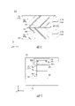
當參照圖1及圖2時,本發明實施形態之裝置10,係獨立之電子設備。更具體說來,裝置10係不物理性地安裝於其他電子設備(未圖示)地,可單獨動作。例如裝置10係藉黏著於對象者的心臟附近,量測對象者之心跳數,傳送量測結果到其他電子設備。亦即,裝置10係可當作量測心跳數等之生物體資訊之電子設備而使用。但是,本發明係並不侷限於此,而可適用於具有種種功能之裝置。When referring to FIG. 1 and FIG. 2 , the
當參照圖1、圖3及圖8時,本實施形態之裝置10係包括電路構造體12、密封構件(薄膜構件)14、及兩個之可壓縮構件60。電路構造體12係用於將裝置10當作電子設備以發揮功能之構件。例如電路構造體12係具有:電子電路(未圖示),用於量測心跳數;以及電子電路(未圖示),用於傳送量測結果到其他電子設備(未圖示)。當參照圖3時,薄膜構件14係使電路構造體12整體與可壓縮構件60整體,一同收容於內部。亦即,電路構造體12及可壓縮構件60,係被封入薄膜構件14內部,薄膜構件14係保護電路構造體12不受外部環境所影響。Referring to FIGS. 1 , 3 and 8 , the
以下,說明本實施形態之裝置10之構造。Next, the structure of the
當參照圖3及圖8時,本實施形態之電路構造體12係包括第1電路構件40、及第2電路構件50。本實施形態之薄膜構件14係包括由絶緣體所構成之第1密封構件20、及由絶緣體所構成之第2密封構件30。本實施形態之可壓縮構件60係包含藉加壓而可壓縮之第1可壓縮構件62、及藉加壓而可壓縮之第2可壓縮構件64。亦即,裝置10係包括第1密封構件20、第2密封構件30、第1電路構件40、第2電路構件50、第1可壓縮構件62、及第2可壓縮構件64。Referring to FIGS. 3 and 8 , the
當參照圖3及圖5時,上述六個構件(第1密封構件20、第2密封構件30、第1電路構件40、第2電路構件50、第1可壓縮構件62及第2可壓縮構件64),係在上下方向(Z方向)中,被堆積重疊,被組立為一個之裝置10。本實施形態之裝置10,係僅包括上述六個構件。但是,本發明係並不侷限於此。例如裝置10也可以在上述六個構件之外,還包括其他構件。例如裝置10也可以還包括附加性電路構件。另外,裝置10也可以係僅包括第1可壓縮構件62及第2可壓縮構件64中之一者。3 and 5, the above-mentioned six members (the
當參照圖8時,本實施形態之第1電路構件40,係具有第1基體42與第1導體線路44。本實施形態之第1基體42,係由絶緣薄膜所構成之矩形之較薄片體,具有可撓性。第1基體42係與直交於Z方向之水平面(片體面:XY平面)平行地延伸。第1導體線路44係被形成於第1基體42上。詳細說來,第1導體線路44係由銅等導電體所構成,藉銀墨印刷或蝕刻等之形成方法,被形成於第1基體42的下表面(-Z側之面)。Referring to FIG. 8 , the
本實施形態之第2電路構件50,係具有第2基體52與第2導體線路54。本實施形態之第2基體52,係由絶緣薄膜所構成之矩形之較薄片體,具有可撓性。第2基體52係與XY平面平行地延伸。第2導體線路54係被形成於第2基體52上。詳細說來,第2導體線路54係由銅等導電體所構成,藉銀墨印刷或蝕刻等之形成方法,被形成於第2基體52的上表面(+Z側之面)。The
本實施形態之第1電路構件40及第2電路構件50之每一個,係具有上述構造。但是,本發明係並不侷限於此。例如在第1電路構件40及第2電路構件50之每一個,也可以設有一個以上之電子零件。第1電路構件40及第2電路構件50中之一者,也可以係單一之電子零件。又,第1基體42及第2基體52之每一個之形狀,係並不侷限於矩形,可因應需要而變形之。第1基體42及第2基體52之每一個,也可以係剛硬(亦即,具有剛性而較難撓曲)之電路基板。第1導體線路44及第2導體線路54之每一個,只要係由導電體所形成,第1導體線路44及第2導體線路54之每一個之形成方法,係並未特別侷限。Each of the
在本實施形態中,第1導體線路44係具有第1接點48,第2導體線路54係具有第2接點58。亦即,第1電路構件40係包括第1接點48,第2電路構件50係包括第2接點58。當參照圖3及圖4時,在被組立後之裝置10中,第1接點48與第2接點58係彼此接觸。亦即,第1電路構件40與第2電路構件50係被組合,使得第1接點48與第2接點58彼此接觸,以形成電路構造體12。電路構造體12的第1導體線路44及第2導體線路54,係彼此被電性連接。In the present embodiment, the
圖8所示之第1導體線路44及第2導體線路54,係用於簡易說明本發明之抽象性導體線路,其不具有具體性功能。亦即,即使圖示之第1接點48與第2接點58彼此接觸,裝置10(參照圖1)也不做為電子設備而發揮功能。另外,實際之第1導體線路44及第2導體線路54,係例如具有圖5及圖6所示之構造。The
當參照圖5及圖6時,於第1基體42的下表面,係形成有第1電路43,在第2基體52的上表面,係形成有第2電路53。第1電路43係具有分別形成有第1接點48之兩個之第1導體線路44、及鈕釦電池46。第2電路53係具有分別形成有第2接點58之兩個之第2導體線路54、及LED(Light Emitting Diode)56。當第1接點48與第2接點58彼此接觸時,電力係自鈕釦電池46被供給到LED56,LED56係發光。第1電路43及第2電路53之構造,係可變形為比圖5及圖6之實施例還要更加實用之構造。例如第2電路53也可以取代LED56,而具有心跳數之量測電路、及量測結果之傳送電路。Referring to FIGS. 5 and 6 , the
當依據圖5及圖6之實施例時,第1接點48及第2接點58之每一個之數量係2。但是,第1接點48及第2接點58之每一個之數量,如圖8所示,也可以係1,或者,3以上。亦即,第1電路構件40係只要包括一個以上之第1接點48即可,第2電路構件50係只要包括分別對應第1接點48之一個以上之第2接點58即可。在被組立後之裝置10中,第1接點48之每一個,係只要與對應之第2接點58相接觸即可。When according to the embodiments of FIGS. 5 and 6 , the number of each of the
當參照圖1~圖3時,本實施形態之第1密封構件20與第2密封構件30,係具有彼此同樣之構造。更具體說來,第1密封構件20及第2密封構件30之每一個,係由薄膜所構成之矩形之較薄片體,具有可撓性。第1密封構件20及第2密封構件30之每一個,係與XY平面平行地延伸。第1密封構件20係具有XY平面中之周緣29。第2密封構件30係具有XY平面中之周緣39。Referring to FIGS. 1 to 3 , the first sealing
本實施形態之第1密封構件20與第2密封構件30,係使XY平面中之周緣29之位置與周緣39之位置彼此一致,以被彼此重疊。但是,本發明係並不侷限於此。例如XY平面中之第1密封構件20之尺寸,與XY平面中之第2密封構件30之尺寸,也可以係彼此不同。第1密封構件20及第2密封構件30之每一個之形狀,係並不侷限於矩形,可因應需要而變形之。The
當參照圖1及圖3時,第1密封構件20係具有第1內側部22與第1外側部24。第1內側部22係在XY平面中,位於第1外側部24的內側。換言之,第1外側部24係在第1密封構件20之中,包圍第1內側部22之部位。第2密封構件30係具有第2內側部32與第2外側部34。第2內側部32係在在XY平面中,位於第2外側部34的內側。換言之,第2外側部34係在第2密封構件30之中,包圍第2內側部32之部位。Referring to FIGS. 1 and 3 , the first sealing
當參照圖3時,第1密封構件20的第1內側部22及第2密封構件30的第2內側部32,係在裝置10中,收容電路構造體12及可壓縮構件60之部位。當一併參照圖3與圖8時,當依據本實施形態時,在裝置10被組立之前,第1密封構件20係沿著XY平面,一氣呵成地延伸,在第1內側部22與第1外側部24之間,沒有可辨識之邊界。同樣地,在裝置10被組立之前,第2密封構件30係沿著XY平面,一氣呵成地延伸,在第2內側部32與第2外側部34之間,沒有可辨識之邊界。但是,本發明係並不侷限於此。例如也可以在第1內側部22與第1外側部24之間,形成有凹陷等之可辨識之邊界,或者,在第2內側部32與第2外側部34之間,形成有凹陷等之可辨識之邊界。Referring to FIG. 3 , the first
當參照圖1及圖3時,本實施形態之第1外側部24,係具有第1密封部26與第1接觸部28。本實施形態之第2外側部34,係具有第2密封部36與第2接觸部38。第1密封部26與第2密封部36係被彼此連接,以形成密封標記16。Referring to FIGS. 1 and 3 , the first
當依據本實施形態時,第1密封部26與第2密封部36,係藉熱封而被彼此連接。亦即,本實施形態之密封標記16,係第1密封部26與第2密封部36藉加熱而彼此熔著之標記。但是,本發明係並不侷限於此,第1密封部26與第2密封部36,係可藉高週波、超音波、雷射、接著等之種種方法連接。例如第1密封部26與第2密封部36,也可以藉接著劑以被彼此連接。在此情形下,密封標記16係接著標記。又,在此情形下,第2密封構件30也可以係具有剛性之比較厚之構件。According to this embodiment, the
本實施形態之密封標記16,係綿延第1密封部26及第2密封部36的全周以被形成。亦即,密封標記16係在XY平面中,綿延全周以包圍第1內側部22及第2內側部32。另外,第1密封部26及第2密封部36的一部份(尤其,XY平面中之外緣),係未被熱封,未形成有密封標記16。但是,本發明係並不侷限於此,密封標記16也可以綿延第1密封部26及第2密封部36整體以被形成。The
當參照圖8時,可壓縮構件60之每一個,係具有反逆性之發泡性緩衝材。更具體說來,本實施形態之可壓縮構件60之每一個,係氨甲酸乙酯泡棉、聚烯烴泡棉、CR(氯丁二烯橡膠)泡棉等之連續氣泡構造體。本實施形態之連續氣泡構造體,係由可伸縮之彈性體、及於彈性體內部稠密地形成之多數氣泡所構成。氣泡係彼此連接以形成連續氣泡。連續氣泡係往彈性體的外部開口。當加壓連續氣泡構造體時,連續氣泡構造體係持續排出氣泡內部的空氣到外部而收縮。當停止往連續氣泡構造體之加壓時,連續氣泡構造體係持續吸收外部空氣到氣泡內部而膨脹,以復原到收縮前之形狀。本實施形態之可壓縮構件60之每一個,係由這種連續氣泡構造體所構成之優良緩衝材。When referring to FIG. 8 , each of the
詳細說來,可壓縮構件60之每一個,係具有本體部602與兩個之主面604。可壓縮構件60之每一個中之兩個之主面604,係在既定方向(在圖8中,係Z方向)中,夾持本體部602以彼此位於相反側,沿著與既定方向直交之平面(在圖8中,係XY平面),彼此平行地延伸。在可壓縮構件60之每一個中,當加壓兩個之主面604,使其於既定方向中,彼此接近以壓縮本體部602時,包含於本體部602之空氣的一部份係被排出,當停止加壓時,空氣流入本體部602。In detail, each of the
本實施形態之可壓縮構件60,係具有上述構造。但是,本發明係並不侷限於此。例如可壓縮構件60也可以形成,使得藉多數彈簧而連接兩片平板,而具有與連續氣泡構造體同樣之功能。The
當一併參照圖3與圖8時,在組立本實施形態之裝置10時,持續壓縮可壓縮構件60,在Z方向中,使第1密封構件20與第2密封構件30彼此接近,使第1密封部26與第2密封部36彼此連接。在壓縮可壓縮構件60時,包含於可壓縮構件60之空氣係被排出。當使第1密封部26與第2密封部36彼此連接時,裝置10的內部係被與外部遮斷。可壓縮構件60之每一個,係吸收殘留於裝置10內部之空氣,藉此,裝置10的內部空間之氣壓係降低。第1接觸部28與第2接觸部38,係藉裝置10內部空間與外部間之氣壓差,於接觸領域17中,彼此接觸。結果,於裝置10形成有被第1內側部22及第2內側部32所包圍之密封空間18。3 and 8, when the
當參照圖1及圖3時,第1密封構件20的第1密封部26及第2密封構件30的第2密封部36,係用於使第1密封構件20及第2密封構件30,藉熱封等之密封而彼此牢固地連接之部位。第1密封構件20的第1接觸部28及第2密封構件30的第2接觸部38,係隨著第1密封部26及第2密封部36之在較低氣壓下之連接,而彼此接觸之部位。當依據本實施形態時,於密封前,在第1密封部26與第1接觸部28之間,沒有可辨識之邊界。同樣地,於密封前,在第2密封部36與第2接觸部38之間,沒有可辨識之邊界。但是,本發明係並不侷限於此。例如也可以於第1密封部26與第1接觸部28之間,形成有凹陷等之可辨識之邊界,也可以於第2密封部36與第2接觸部38之間,形成有凹陷等之可辨識之邊界。1 and 3 , the
當依據本實施形態時,第1密封部26與第2密封部36,係於使密封空間18內部之氣壓,為比大氣壓還要低之較低氣壓後之狀態下,彼此連接。而且,接觸領域17係在XY平面中,綿延全周以無縫地包圍第1內側部22及第2內側部32,藉此,遮斷密封空間18內部與外部間之空氣之流動。亦即,密封空間18內部之氣壓,在被彼此連接之第1密封部26及第2密封部36之外,還藉被彼此密著之第1接觸部28及第2接觸部38,被維持使得成為比大氣壓還要低之較低氣壓。但是,本發明係並不侷限於此。例如接觸領域17也可以係使第1內側部22及第2內側部32,在XY平面中,局部性地包圍。According to this embodiment, the
當參照圖3時,可壓縮構件60係被封入被維持於上述較低氣壓之密封空間18內部。第1可壓縮構件62係在Z方向中,位於第1密封構件20與第1電路構件40之間。第2可壓縮構件64係在Z方向中,位於第2密封構件30與第2電路構件50之間。When referring to FIG. 3 , the
當參照圖3時,第1電路構件40及第2電路構件50係與可壓縮構件60,一同被封入被維持於上述較低氣壓之密封空間18內部。當組立裝置10時,第1密封構件20係加壓第1可壓縮構件62,而往第1電路構件40壓抵,第2密封構件30係加壓第2可壓縮構件64,而往第2電路構件50壓抵。當參照圖3及圖8時,此時,可壓縮構件60之每一個,係持續排出本體部602之空氣,主要係在既定方向(Z方向)上,被壓縮。亦即,於被組立後之裝置10的可壓縮構件60之每一個中,包含於本體部602之空氣的一部份係被排出。因此,裝置10中之可壓縮構件60之每一個之厚度(Z方向中之尺寸),係在與壓縮前之可壓縮構件60(參照圖8)比較下,非常薄。Referring to FIG. 3 , the
當參照圖3及圖4時,第1接點48與第2接點58,係在密封空間18內部,彼此接觸。詳細說來,被封入密封空間18內之可壓縮構件60,係吸收殘留於密封空間18之少許空氣。結果,密封空間18之氣壓係降低。第1接點48與第2接點58,係因為密封空間18內部與外部間之氣壓差,而被彼此壓抵,同時藉可壓縮構件60之復原力,而被彼此壓抵。第2接點58係藉被壓縮後之第2可壓縮構件64之復原力,被壓抵到第1接點48。亦即,第1接點48與第2接點58,係藉可壓縮構件60之復原力,而被彼此壓抵。因此,第1接點48與第2接點58間之接觸係被確實地維持。Referring to FIGS. 3 and 4 , the
當總結以上之說明時,在本實施形態之裝置10中,第1密封構件20及第2密封構件30,係夾持電路構件(第1電路構件40及第2電路構件50)及可壓縮構件60於其間,以被重疊使得彼此接觸。第1密封構件20及第2密封構件30之每一個,係由較薄之薄膜所構成。可壓縮構件60係可藉加壓而壓縮以變薄。又,電路構件之每一個,係除了包括接點(第1接點48或第2接點58),在構造上沒有限制。亦即,本實施形態之電路構件,係具有簡易之構造,可由種種材料形成。例如電路構件也可以係形成有具有接點之導體線路(第1導體線路44或第2導體線路54)之絶緣薄膜。在此情形下,可使裝置10整體之厚度非常薄。亦即,當依據本實施形態時,可提供可薄型化之嶄新之裝置10。To summarize the above description, in the
本實施形態之可壓縮構件60,係包含第1可壓縮構件62及第2可壓縮構件64。當依據本實施形態時,配置第1可壓縮構件62及第2可壓縮構件64,使得夾入第1接點48及第2接點58,藉此,可使第1接點48與第2接點58,更穩定地連接。但是,本發明係並不侷限於此。例如可壓縮構件60也可以僅包含第1可壓縮構件62及第2可壓縮構件64中之任一者。又,第1可壓縮構件62及第2可壓縮構件64之每一個之數量,也可以係兩個以上。亦即,裝置10係只要包括一個以上之可壓縮構件60即可。可壓縮構件60係只要包含第1可壓縮構件62及第2可壓縮構件64中之至少一者即可。The
當參照圖3及圖8時,本實施形態之第1可壓縮構件62,係除了第1電路構件40的端部,覆蓋第1電路構件40整體。本實施形態之第2可壓縮構件64,係除了第2電路構件50的端部,覆蓋第2電路構件50整體。亦即,可壓縮構件60之每一個,係在XY平面中,與第1接點48及第2接點58之每一個相比較下,具有非常大之尺寸(面積)。具有如此大之面積之可壓縮構件60之每一個係很容易配置,使得與第1接點48及第2接點58相對應。Referring to FIGS. 3 and 8 , the first
壓縮前之可壓縮構件60之每一個,係在XY平面中,不僅具有較大之尺寸,於Z方向中,具有較大之尺寸。換言之,本實施形態之壓縮前之可壓縮構件60之每一個,係具有較大之體積。當使用裝置10時,空氣進入密封空間18內部時,空氣係被可壓縮構件60所吸收,藉此,可壓縮構件60之復原力係減少。但是,本實施形態之可壓縮構件60之每一個係較大,所以,可使復原力之改變較小。Each of the
但是,本發明係並不侷限於此。只要可使第1接點48及第2接點58彼此壓抵,以封入可壓縮構件60到密封空間18內部,可壓縮構件60之每一個之尺寸及形狀係並未特別侷限。例如第1可壓縮構件62也可以僅位於第1密封構件20與第1接點48之間。第2可壓縮構件64也可以僅位於第2密封構件30與第2接點58之間。亦即,第1可壓縮構件62係只要至少局部性地位於第1密封構件20與第1接點48之間即可。第2可壓縮構件64係只要至少局部性地位於第2密封構件30與第2接點58之間即可。However, the present invention is not limited to this. The size and shape of each of the
本實施形態之裝置10,係包括可壓縮構件60,所以,當組立裝置10後,於第1接點48與第2接點58之間,係產生起因於可壓縮構件60之復原力之接觸力。而且,可使第1接點48與第2接點58間之接觸力,綿延長期間而穩定地維持。又,可壓縮構件60係當作緩衝材而發揮功能,所以,裝置10係即使彎曲也較難破損。當依據本實施形態時,可提供在種種環境中,綿延長期間,可穩定地動作之裝置10。The
當參照圖1及圖3時,當依據本實施形態時,第1接觸部28及第2接觸部38,係在XY平面中,綿延全周以無縫地包圍第1內側部22及第2內側部32。第1密封部26及第2密封部36,係在XY平面中,綿延全周以無縫地包圍第1接觸部28及第2接觸部38。當依據此構造時,密封空間18之氣密性係可確實地維持。而且,藉切除第1密封部26及第2密封部36,可自密封空間18,容易地取出第1電路構件40及第2電路構件50。亦即,當依據本實施形態時,可容易地分別回收構件,而且,可再利用。但是,本發明係並不侷限於此。例如第1密封部26及第2密封部36,係也可以在XY平面中,局部性地包圍第1接觸部28及第2接觸部38。第1接觸部28及び第2接觸部38,係可以局部性地形成,也可以未形成。Referring to FIGS. 1 and 3 , according to the present embodiment, the
當參照圖1及圖11時,本實施形態之第1密封構件20及第2密封構件30之每一個,係包括藉熱封而熔融之熔融層146、及不藉熱封而熔融之非熔融層148。亦即,第1密封部材20及第2密封構件30之每一個,係具有由熔融層146及非熔融層148所構成之雙層構造。例如熔融層146係由聚乙烯所構成,非熔融層148係由尼龍所構成。藉此構造,可持續維持第1密封部26及第2密封部36的非熔融層148,使熔融層146彼此熔著。但是,本發明係並不侷限於此、第1密封構件20及第2密封構件30之每一個,係只要具有對應密封方法之構造即可。例如第1密封構件20及第2密封構件30之每一個,也可以僅包括一層,也可以包括三層以上之層。1 and 11, each of the first sealing
本實施形態之第1密封構件20及第2密封構件30之每一個,係在第1密封部26及第2密封部36以外之部位,也包括熔融層146與非熔融層148。但是,本發明係並不侷限於此。例如熔融層146也可以僅形成於第1密封部26及第2密封部36之每一個。Each of the first sealing
當參照圖1時,第1密封構件20及第2密封構件30之每一個,最好係具有較高之氧阻隔性。更具體說來,第1密封構件20及第2密封構件30之每一個,係最好包括由具有較高氧阻隔性之材料(高氧阻隔材)所構成之層。當依據此層構造時,可減少電路構造體12的金屬構件之氧化。When referring to FIG. 1 , it is preferable that each of the first sealing
例如高氧阻隔材也可以係線性聚乙烯(LLDPE : Linear Low Density Polyethylene)。更具體說來,高氧阻隔材也可以係覆膜加工聚對苯二甲酸乙二酯、鋁及聚乙烯後之PET/AI/PE,也可以係覆膜加工雙軸延伸尼龍及聚乙烯後之ON/PE,也可以係覆膜加工聚對苯二甲酸乙二酯、聚氯乙烯及聚乙烯後之PET/EVOH/PE,也可以係覆膜加工透明高阻隔薄膜及聚乙烯以形成之。透明高阻隔薄膜也可以係SiOx蒸著PET(聚對苯二甲酸乙二酯),也可以係氧化鋁蒸著PET(聚對苯二甲酸乙二酯)。For example, the high oxygen barrier material may also be linear polyethylene (LLDPE: Linear Low Density Polyethylene). More specifically, the high oxygen barrier material can also be PET/AI/PE after laminating and processing polyethylene terephthalate, aluminum and polyethylene, or can be laminating and processing biaxially stretched nylon and polyethylene. The ON/PE can also be PET/EVOH/PE after laminating and processing polyethylene terephthalate, polyvinyl chloride and polyethylene, or it can be laminating and processing transparent high-barrier film and polyethylene. . The transparent high-barrier film may be SiOx vaporized PET (polyethylene terephthalate) or alumina vaporized PET (polyethylene terephthalate).
本實施形態之第1密封構件20及第2密封構件30之每一個,最好在具有較高之氧阻隔性之外,還具有較高之水蒸氣阻隔性。更具體說來,第1密封構件20及第2密封構件30之每一個,最好係包括由具有較高之水蒸氣阻隔性之材料(高水蒸氣阻隔材)所構成之層。當依據此層構造時,可使電路構造體12防水。例如高水蒸氣阻隔材也可以係在ON/PE、OPP(雙軸延伸聚丙烯)、PET等之片體,施加過PVDC(聚偏二氯乙烯)塗層之材料。It is preferable that each of the first sealing
第1密封構件20及第2密封構件30之每一個,也可以在具有較高之氧阻隔性及較高之水蒸氣阻隔性之外,還具有氮阻隔性等之種種阻隔性。亦即,第1密封構件20及第2密封構件30之每一個,最好係具有因應用途之較高之阻隔性。Each of the first sealing
當參照圖7時,本實施形態之裝置10(參照圖1),係經過準備工序(步驟1)、配置工序(步驟2)、及密封工序(步驟3)之三個工序以被製造。但是,本發明係並不侷限於此、裝置10之製造方法,係可因應需要而變形之。以下,說明本實施形態之裝置10之製造方法。Referring to FIG. 7 , the device 10 (refer to FIG. 1 ) of the present embodiment is manufactured through three steps of a preparation step (step 1 ), an arrangement step (step 2 ), and a sealing step (step 3 ). However, the present invention is not limited to this, and the manufacturing method of the
當參照圖8時,於準備工序(參照圖7)中,準備裝置構件11。裝置構件11係包括第1密封構件20、第2密封構件30、第1電路構件40、第2電路構件50、及可壓縮構件60。各構件係具有已經說明過之構造,如已經說明過地,可做種種變形。Referring to FIG. 8 , in a preparation step (see FIG. 7 ), the
亦即,本實施形態之製造方法,係包括準備工序,準備第1密封構件20、第2密封構件30、第1電路構件40、第2電路構件50及可壓縮構件60,其中,第1密封構件20係由薄膜所構成,第1電路構件40係包括第1接點48,第2電路構件50係包括第2接點58,可壓縮構件60係包含第1可壓縮構件62及第2可壓縮構件64中之至少一者,可壓縮構件60之每一個,係具有本體部602與兩個之主面604,可壓縮構件60之每一個中之兩個之主面604,係在既定方向(在圖8中,係Z方向)中,夾持本體部602而彼此位於相反側,於可壓縮構件60之每一個中,當加壓使得兩個主面604在既定方向中,彼此接近,以壓縮本體部602時,包含於本體部602之空氣的一部份係被排出,當停止加壓時,空氣流入本體部602。That is, the manufacturing method of the present embodiment includes a preparation step of preparing the first sealing
接著,當參照圖9~圖11時,於配置工序(參照圖7)中,沿著Z方向,自上而下,依序重疊第1密封構件20、第1電路構件40、第2電路構件50及第2密封構件30。此時,使第1電路構件40及第2電路構件50,位於第1密封構件20及第2密封構件30之XY平面中之中間部。配置第1電路構件40及第2電路構件50,使得第1接點48與第2接點58在Z方向中,相向。配置第1可壓縮構件62及第2可壓縮構件64,使得上下夾持第1電路構件40的第1接點48及第2電路構件50的第2接點58。又,配置第1密封構件20及第2密封構件30,使得兩個之熔融層146在Z方向中,相向。Next, referring to FIGS. 9 to 11 , in the arrangement step (see FIG. 7 ), the first sealing
接著,當參照圖9~圖12時,收容如上所述地配置之裝置構件11於組立裝置70內部。亦即,本實施形態之製造方法,係包括配置工序,依序重疊第1密封構件20、第1電路構件40、第2電路構件50及第2密封構件30,使第1接點48與第2接點58相向,其中,使第1可壓縮構件62至少局部性地位於第1密封構件20與第1接點48之間,使第2可壓縮構件64至少局部性地位於第2密封構件30與第2接點58之間,配置於組立裝置70內。Next, referring to FIGS. 9 to 12 , the
當參照圖12時,本實施形態之組立裝置70,係包括模具74、加壓部76、及熱封棒78。裝置構件11係被置於模具74之上。之後,使組立裝置70的加壓部76與熱封棒78一同移動到下方,持續加壓裝置構件11,壓抵到模具74。藉加壓部76之加壓,可壓縮構件60之每一個,係持續排出內部的空氣,主要係於Z方向上,被壓縮。當可壓縮構件60之每一個被充分地壓縮後,藉熱封棒78密封第1密封構件20與第2密封構件30。Referring to FIG. 12 , the assembling
詳細說來,本實施形態之熱封條78,係具有加熱部782。當依據本實施形態時,係加熱加熱部782,使得成為熔融層146(參照圖11)之熔點以上之高溫。壓抵如此加熱後之加熱部782,到被上下重疊之第1密封構件20的第1密封部26及第2密封構件30的第2密封部36,以熱封第1密封部26與第2密封部36。Specifically, the
熱封之結果,第1電路構件40、第2電路構件50及可壓縮構件60,係被封入被第1密封構件20及第2密封構件30所包圍之密封空間18(參照圖3)內。當熱封後,停止由加壓部76所做之加壓時,可壓縮構件60係回到原來之形狀,以吸收密封空間18的空氣。吸收空氣後之可壓縮構件60係膨脹,藉此,密封空間18之體積係變大,密封空間18之氣壓係下降。結果,在密封空間18內部與外部之間產生氣壓差,而產生壓縮可壓縮構件60之壓縮力。在此壓縮力與可壓縮構件60之復原力均衡後,可壓縮構件60之膨脹係結束。As a result of heat sealing, the
當可壓縮構件60之膨脹結束後,可壓縮構件60係未回到原來之形狀,具有復原力。第1接點48與第2接點58,係藉因為密封空間18(參照圖3)的內部與外部間之氣壓差,所產生之可壓縮構件60之復原力,而被彼此壓抵。結果,第1接點48與第2接點58係彼此確實地接觸。After the expansion of the
亦即,本實施形態之製造方法,係包括密封工序,其持續壓縮可壓縮構件60,使第1密封構件20與第2密封構件30彼此接觸以密封,藉此,使第1電路構件40、第2電路構件50及可壓縮構件60,封入被第1密封構件20及第2密封構件30所包圍之密封空間18(參照圖3)內,而且,使第1接點48與第2接點58彼此接觸。That is, the manufacturing method of the present embodiment includes a sealing step of continuously compressing the
當參照圖3時,當依據本實施形態之製造方法時,第1接點48與第2接點8係不藉軟焊等而彼此固定地,彼此確實地接觸。因此,當無須裝置10時,僅藉切除第1密封部26及第2密封部36,就可分解裝置10。而且,可封入第1電路構件40及第2電路構件50到較低氣壓之密封空間18內部,藉此,可減少由金屬構件之氧化等所致之劣化。但是,本發明係並不侷限於此,裝置10之製造方法及密封方法,係可因應需要而變形之。Referring to FIG. 3, according to the manufacturing method of the present embodiment, the
當參照圖7~圖12時,當依據上述製造方法時,藉自準備工序至密封工序為止之工序,由一個之裝置構件11製造一個之裝置10(參照圖1)。但是,本發明係並不侷限於此。例如當參照圖13時,也可以係準備及配置包括複數之裝置構件11之構件,對於此構件整體實施密封工序(參照圖7及圖12)。又,也可以藉滾輪等,傳遞圖13所示之構件到組立裝置70(參照圖12)內部。Referring to FIGS. 7 to 12 , according to the above-described manufacturing method, a single device 10 (see FIG. 1 ) is manufactured from a
本實施形態係在已經說明過之變形例之外,還可做種種變形。以下,說明五個變形例。The present embodiment can be modified in various ways in addition to the modifications already described. Hereinafter, five modified examples will be described.
當比較圖14與圖5時,本實施形態之第1變形例之裝置10A係包括:電路構造體12A,與裝置10的電路構造體12不同;密封構件14A,與裝置10的密封構件14不同;以及可壓縮構件60A,與裝置10的可壓縮構件60不同。密封構件14A係與密封構件14同樣地,使電路構造體12A與可壓縮構件60A一同收容於內部。14 and FIG. 5 , the
本變形例之密封構件14A係包括:第1密封構件20,由與裝置10同樣之薄膜所構成;以及第2密封構件(基板)30A。第2密封構件30A係剛硬之電路基板。本變形例之電路構造體12A,係包括第1電路構件40A與第2電路構件50A。第1電路構件40A係單一之電子零件,包括兩個之第1接點48A。第2電路構件50A係被形成於第2密封構件30A之導體線路,包括兩個之第2接點58A。第1接點48A係分別與第2接點58A相接觸,藉此,被形成於第2密封構件30A之導體線路係導通。可壓縮構件60A係僅包含一個之第1可壓縮構件62A。第1壓縮可能構件62A係與第1可壓縮構件62同樣之連續氣泡構造體。The sealing
如上所述,裝置10A係包括第1密封構件20、第2密封構件30A、第1電路構件40A、第2電路構件50A、及一個之可壓縮構件60A。第1密封構件20及第2密封構件30A,係例如藉接著劑而被密封。但是,本發明係並不侷限於此。例如也可以第1密封構件20及第2密封構件30A係被熱封。在此情形下,也可以第2密封構件30A係與第1密封構件20同樣地,包括藉熱封而熔融之熔融層(未圖示)、及不藉熱封而熔融之非熔融層(未圖示)。又,第2密封構件30A也可以係與第1密封構件20同樣地,具有較高之氧阻隔性、及較高之水蒸氣阻隔性等之較高之阻隔性。As described above,
在裝置10A係形成有與裝置10同樣之密封空間18。第1電路構件40A及第2電路構件50A係與可壓縮構件60A一同,被封入密封空間18內部。可壓縮構件60A係位於第1密封構件20與包含第1接點48A之第1電路構件40A整體之間,使第1接點48A分別壓抵於第2接點58A。當依據本變形例時,使第1電路構件40A不藉軟焊等而固定於第2電路構件50A地,可穩定地連接第1接點48A與第2接點58A。In the
當比較圖15與圖14時,本實施形態之第2變形例之裝置10B係包括:電路構造體12B,與裝置10A的電路構造體12A不同;密封構件14B,與裝置10A的密封構件14A不同;以及可壓縮構件60B,與裝置10A的可壓縮構件60A不同。密封構件14B係與密封構件14A同樣地,使電路構造體12B與可壓縮構件60B一同收容於內部。15 and FIG. 14, the
本變形例之密封構件14B係包括:第1密封構件20,由與裝置10A相同之薄膜所構成;以及第2密封構件(基板)30B,與裝置10A的第2密封構件30A同樣之剛硬電路基板。本變形例之電路構造體12B,係包括第1電路構件40B與第2電路構件50B。第1電路構件40B係由單一之電子零件41B所構成。電子零件41B係包括主部42B與兩個之端子49B。端子49B之每一個,係當作第1接點48B而發揮功能。第2電路構件50B係被形成於第2密封構件30B之導體線路,其包括分別與第1接點48B相對應之兩個之第2接點58B。可壓縮構件60B係僅包含分別與第1接點48B相對應之兩個之第1可壓縮構件62B。第1可壓縮構件62B之每一個,係與第1可壓縮構件62A同樣之連續氣泡構造體。The sealing
如上所述,裝置10B係包括第1密封構件20、第2密封構件30B、第1電路構件40B、第2電路構件50B、及兩個之可壓縮構件60B。第1密封構件20及第2密封構件30B,係例如藉接著劑而被密封。在裝置10B係形成有與裝置10A同樣之密封空間18。第1電路構件40B及第2電路構件50B,係與兩個之可壓縮構件60B一同,被封入密封空間18的內部。第1接點48B係分別與第2接點58B相接觸。As described above, the
可壓縮構件60B之每一個,係位於對應之第1接點48B與第1密封構件20之間,使端子49B的第1接點48B壓抵到第2接點58B。端子49B之每一個,係被設於主部42B的下部,朝向對應之第2接點58B而往下方延伸。可壓縮構件60B之每一個,係不覆蓋主部42B,而覆蓋對應之端子49B。Each of the
當依據本變形例時,與裝置10A同樣地,使第1電路構件40B不藉軟焊等以固定於第2電路構件50B地,可穩定地連接第1接點48B與第2接點58B。又,當依據本變形例時,可使可壓縮構件60B之XY平面中之尺寸,小於第1電路構件40B整體。According to this modification, the
本變形例係還可變形。例如電子零件41B之數量也可以係兩個以上。第1電路構件40B也可以係剛硬之電路基板。在此情形下,第2電路構件50B也可以係單一之電子零件41B。亦即,第1電路構件40B及第2電路構件50B中之至少一者,也可以包含電子零件41B。電子零件41B的端子49B係只要當作第1接點48B及第2接點58B中之一者以發揮功能即可。又,電子零件41B的端子49B,只要係自主部42B往第1接點48B及第2接點58B中之另一者延伸即可。可壓縮構件60B中之一個,也可以係不覆蓋主部42B,而覆蓋端子49B。This modification can also be modified. For example, the number of
當比較圖16與圖10時,本實施形態之第3變形例之裝置構件11C係包括:電路構造體12C,與裝置構件11的電路構造體12不同;密封構件(薄膜構件)14,與裝置構件11相同;以及可壓縮構件60C,與裝置構件11的可壓縮構件60不同。薄膜構件14係與裝置10(參照圖1)同樣地被熱封。在於裝置構件11C所組立後之裝置(未圖示),係形成有與裝置10同樣之密封空間18(參照圖3)。16 and FIG. 10, the
本變形例之電路構造體12C,係包括第1電路構件40C與第2電路構件50C。第1電路構件40C係包括與第1電路構件40同樣之第1基體42、被形成於第1基體42之第1導體線路44、及被連接於第1導體線路44之電子零件471C。第2電路構件50C係包括與第2電路構件50同樣之第2基體52、被形成於第2基體52之第2導體線路54、及被連接於第2導體線路54之電子零件571C。可壓縮構件60C係包含三個之第1可壓縮構件62C、及三個之第2可壓縮構件64C。可壓縮構件60C之每一個,係與可壓縮構件60同樣之連續氣泡構造體。The
第1電路構件40C係包括四個之第1接點48C。第1接點48C中之三個,係被設於第1導體線路44。第1接點48C中之另一個,係被設於電子零件471C。第2電路構件50C係包括分別對應於第1接點48C之四個之第2接點58C。第2接點58C中之兩個,係被設於第2導體線路54。第2接點58C中之另兩個,係被設於電子零件571C。The
由圖16可以理解到:由裝置構件11C所組立之裝置(未圖示)係包括第1密封構件20、第2密封構件30、第1電路構件40C、第2電路構件50C、及六個之可壓縮構件60C。第1電路構件40C及第2電路構件50C,係與六個之可壓縮構件60C一同,被封入裝置的密封空間18(參照圖3)內部。第1接點48C係分別與第2接點58C相接觸。第1可壓縮構件62C之每一個,係位於對應之第1接點48C與第1密封構件20之間,壓抵第1接點48C到對應之第2接點58C。第2可壓縮構件64C之每一個,係位於對應之第2接點58C與第2密封構件30之間,壓抵第2接點58C到對應之第1接點48C。It can be understood from FIG. 16 that the device (not shown) formed by the
當依據本變形例時,與裝置10同樣地,對於包含電子零件471C之第1電路構件40C及包含電子零件571C之第2電路構件50C,不施加軟焊等地,可分別穩定地連接第1接點48C到第2接點58C。又,當依據本變形例時,可使可壓縮構件60C之Z方向中之尺寸,因應第1接點48C與第2接點58C間之距離而調整。例如第1導體線路44的第1接點48C與第2導體線路54的第2接點58C,係與其他第1接點48C及第2接點58C相比較下,彼此較大地遠離。在此情形下,只要加大對應之可壓縮構件60C之Z方向中之尺寸,以加大可壓縮構件60C被壓縮後之復原力即可。藉這種調整,可使裝置10B整體之厚度為均等,可分別穩定地連接第1接點48C到第2接點58C。According to this modification, similarly to the
當比較圖17與圖8時,本實施形態之第4變形例之裝置10D,係由裝置構件11D所製造。裝置構件11D係取代裝置構件11的第1密封構件20及第2密封構件30,而包括由絶緣體所構成之一片之薄膜構件(平面片體)14D,而且,其包括與裝置構件11相同之電路構造體12、及比裝置構件11的可壓縮構件60還要小之可壓縮構件(未圖示)。When comparing FIG. 17 and FIG. 8 , the
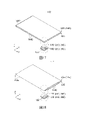
平面片體14D係在前後方向(X方向)中之中間部(既定部142D)中,被彎折,藉此,形成有在Z方向中,彼此重疊之第1密封構件(密封片)20D與第2密封構件(密封片)30D。亦即,第1密封構件20D及第2密封構件30D,係在一片之薄膜構件14D中,被彼此重疊之兩片密封片。薄膜構件14D係一片平面片體,具有既定部142D與端緣144D。端緣144D係薄膜構件14D之XY平面中之緣。The
本變形例之裝置10D,係可藉與裝置10(參照圖1)同樣之製造方法,製造為同樣之構造。例如在配置工序(參照圖7)中,電路構造體12及可壓縮構件,係被配置於Z方向中之第1密封構件20D與第2密封構件30D之間。又,第1密封部26D與第2密封部36D,係被彼此連接以形成密封標記16D。第1接觸部28D與第2接觸部38D係在接觸領域17D中,彼此接觸。於裝置10D係形成有與裝置10(參照圖3)同樣之密封空間18(參照圖3)。第1電路構件40、第2電路構件50及可壓縮構件,係被封入密封空間18的內部。第1電路構件40的第1接點48與第2電路構件50的第2接點58,係藉可壓縮構件而被彼此壓抵以接觸。The
另外,裝置10D係在以下之點中,與裝置10(參照圖1)不同。首先,第1密封構件20D及第2密封構件30D係在既定部142D中,被彎折重疊之兩片密封片。亦即,第1密封構件20D及第2密封構件30D,係在既定部142D中,彼此連接。當依據此構造時,既定部142D與接觸領域17D之間,係無須密封。因此,僅接觸領域17D與端緣144D間係被密封。亦即,密封標記16D係僅被形成於接觸領域17D與端緣144D之間。但是,本發明係並不侷限於此,也可以密封既定部142D與接觸領域17D之間。亦即,密封標記16D係只要至少被形成於接觸領域17D與端緣144D之間即可。In addition, the
當比較圖18與圖8時,本實施形態之第5變形例之裝置10E,係由裝置構件11E所製造。裝置構件11D係取代裝置構件11的第1密封構件20及第2密封構件30,而包括由絶緣體所構成之一片之薄膜構件(袋狀片體)14E,而且,其包括與裝置構件11相同之電路構造體12、及比裝置構件11的可壓縮構件60還要小之可壓縮構件(未圖示)。When comparing FIG. 18 with FIG. 8 , the
袋狀片體14E係在XY平面中之三邊(既定部142E)中,連接,在前端(+X側之端)中,開口。藉此構造,於袋狀片體14E係形成有在Z方向中,彼此重疊之第1密封構件(密封片)20E與第2密封構件(密封片)30E。亦即,第1密封構件20E及第2密封構件30E,係在一片之薄膜構件14E中,被彼此重疊之兩片密封片。薄膜構件14E係一片袋狀片體,其具有既定部142E與端緣144E。端緣144E係薄膜構件14E的開口部的緣。The bag-
本變形例之裝置10E,係可藉與裝置10(參照圖1)同樣之製造方法,製造為同樣之構造。例如在配置工序(參照圖7)中,電路構造體12及可壓縮構件,係被封入薄膜構件14E的內部,被配置於Z方向中之第1密封構件20E與第2密封構件30E之間。又,第1密封部26E與第2密封部36E,係被彼此連接以形成密封標記16E。第1接觸部28E與第2接觸部38E,係在接觸領域17E中,彼此接觸。於裝置10E係形成有與裝置10(參照圖3)同樣之密封空間18。第1電路構件40、第2電路構件50及可壓縮構件,係被封入密封空間18內部。第1電路構件40的第1接點48與第2電路構件50的第2接點58,係藉可壓縮構件而被彼此壓抵以接觸。The
另外,裝置10E係在以下之點中,與裝置10(參照圖1)不同。首先,第1密封構件20E及第2密封構件30E,係在既定部142E中,彼此連接之兩片密封片。亦即,第1密封構件20E及第2密封構件30E,係在既定部142E中,彼此連接。當依據此構造時,既定部142E與接觸領域17E之間,係無須密封。因此,僅接觸領域17E與端緣144E間係被密封。亦即,密封標記16E係僅被形成於接觸領域17E與端緣144E之間。但是,本發明係並不侷限於此,也可以密封既定部142E與接觸領域17E之間。亦即,密封標記16E係只要至少被形成於接觸領域17E與端緣144E之間即可。In addition, the
在上述之第4及第5變形例中,薄膜構件係一片平面片體或一片袋狀片體。但是,本發明之薄膜構件係並不侷限於此,而可做種種變形。In the above-mentioned fourth and fifth modification examples, the film member is a flat sheet or a bag-like sheet. However, the film member of the present invention is not limited to this, and various modifications can be made.
10,10A,10B,10D,10E:裝置 11,11C,11D,11E:裝置構件 12,12A,12B,12C:電路構造體 14:密封構件(薄膜構件) 14A:密封構件 14B:密封構件 14D:薄膜構件(平面片體) 14E:薄膜構件(袋狀片體) 142D,142E:既定部 144D,144E:端緣 146:熔融層 148:非熔融層 16,16D,16E:密封標記 17,17D,17E:接觸領域 18:密封空間 20:第1密封構件 20D,20E:第1密封構件(密封片) 22:第1內側部 24:第1外側部 26,26D,26E:第1密封部 28,28D,28E:第1接觸部 29:周緣 30:第2密封構件 30A,30B:第2密封構件(基板) 30D,30E:第2密封構件(密封片) 32:第2內側部 34:第2外側部 36,36D,36E:第2密封部 38,38D,38E:第2接觸部 39:周緣 40,40A,40B,40C:第1電路構件 41B:電子零件 42:第1基體 42B:主部 43:第1電路 44:第1導體線路 46:鈕釦電池 471C:電子零件 48,48A,48B,48C:第1接點 49B:端子 50,50A,50B,50C:第2電路構件 52:第2基體 53:第2電路 54:第2導體線路 56:LED 571C:電子零件 58,58A,58B,58C:第2接點 60,60A,60B,60C:可壓縮構件 602:本體部 604:主面 62,62A,62B,62C:第1可壓縮構件 64,64C:第2可壓縮構件 70:組立裝置 74:模具 76:加壓部 78:熱封棒 782:加熱部 10, 10A, 10B, 10D, 10E: Devices 11, 11C, 11D, 11E: Device Components 12, 12A, 12B, 12C: Circuit Constructs 14: Sealing member (film member) 14A: Sealing member 14B: Sealing member 14D: Thin film member (plane sheet) 14E: Film member (bag-shaped sheet) 142D, 142E: Established Department 144D, 144E: Edge 146: Melted Layer 148: non-melting layer 16, 16D, 16E: Seal mark 17, 17D, 17E: Contact Fields 18: Sealed space 20: 1st sealing member 20D, 20E: 1st sealing member (sealing sheet) 22: 1st inner part 24: 1st outer part 26, 26D, 26E: 1st seal 28, 28D, 28E: 1st contact part 29: Perimeter 30: Second sealing member 30A, 30B: Second sealing member (substrate) 30D, 30E: Second sealing member (sealing sheet) 32: 2nd inner part 34: 2nd outer part 36, 36D, 36E: 2nd seal 38, 38D, 38E: 2nd contact part 39: Perimeter 40, 40A, 40B, 40C: 1st circuit member 41B: Electronic Parts 42: 1st Matrix 42B: Main Department 43: Circuit 1 44: 1st conductor line 46: Button battery 471C: Electronic Parts 48, 48A, 48B, 48C: 1st contact 49B: Terminal 50, 50A, 50B, 50C: 2nd circuit member 52: 2nd matrix 53: 2nd circuit 54: 2nd conductor line 56: LED 571C: Electronic Parts 58, 58A, 58B, 58C: 2nd contact 60, 60A, 60B, 60C: Compressible members 602: Body part 604: Main side 62, 62A, 62B, 62C: 1st compressible member 64,64C: 2nd compressible member 70: Assembly device 74: Mold 76: Pressurizing part 78: Heat sealing rod 782: Heating Department
〔圖1〕係表示本發明實施形態之裝置之立體圖。以虛線描繪被形成於第1密封構件與第2密封構件間之接觸領域的邊界。放大描繪裝置的一部份(以中心線包圍之部分)。 〔圖2〕係表示圖1之裝置之側視圖。 〔圖3〕係沿著III-III線,表示圖2之裝置之剖面圖。放大描繪裝置的一部份(以中心線包圍之兩個部分)。在放大圖中之一個中,以虛線描繪接觸領域的邊界。 〔圖4〕係更放大表示圖3之放大圖中之裝置的一部份(以假想線A包圍之部分)之剖面圖。 〔圖5〕係概略表示圖3之裝置之具體例之剖面圖。 〔圖6〕係概略表示圖5之裝置的第1電路構件的第1導體線路及第2電路部材的第2導體線路之圖。圖示之第1電路的第1接點,雖然遠離第2電路的第2接點,但是,第1接點係實際上,位於第2接點之上。 〔圖7〕係表示圖1之裝置之製造方法例之圖。 〔圖8〕係表示以圖7之製造方法之準備工序所準備之裝置構件之立體圖。以虛線描繪隱藏之第1電路之輪廓。 〔圖9〕係表示以圖7之製造方法之配置工序所配置之圖8之裝置構件之立體圖。 〔圖10〕係表示圖9之裝置構件之側視圖。 〔圖11〕係沿著XI-XI線,表示圖10之裝置構件之剖面圖。放大描繪裝置構件的一部份(以虛線包圍之兩個部分)。 〔圖12〕係使在圖7之製造方法之配置工序中,被配置於組立裝置內之圖10之裝置構件,與組立裝置之示意性構造一同表示之圖。 〔圖13〕係表示包括複數個圖9之裝置構件之構件之立體圖。以虛線描繪裝置構件間之邊界。 〔圖14〕係表示圖5之裝置之變形例之剖面圖。 〔圖15〕係表示圖5之裝置之另一變形例之剖面圖。 〔圖16〕係表示圖5之裝置之又一變形例中之裝置構件之剖面圖。 〔圖17〕係表示圖8之裝置構件的薄膜構件之變形例之立體圖。針對薄膜構件的一部份(以虛線包圍之部分),描繪裝置被組立後之構造。 〔圖18〕係表示圖8之裝置構件的薄膜構件之另一變形例之立體圖。針對薄膜構件的一部份(以虛線包圍之部分),描繪裝置被組立後之構造。 〔圖19〕係表示專利文獻1之裝置之剖面圖。 [FIG. 1] is a perspective view showing an apparatus according to an embodiment of the present invention. The boundary of the contact area formed between the first sealing member and the second sealing member is drawn with a broken line. Enlarge part of the depiction device (the part enclosed by the center line). [Fig. 2] is a side view showing the apparatus of Fig. 1. [Fig. [FIG. 3] is a sectional view of the apparatus of FIG. 2 taken along the line III-III. Enlarge part of the depiction device (two parts surrounded by a center line). In one of the enlarged figures, the boundaries of the contact area are delineated by dashed lines. [FIG. 4] is a cross-sectional view showing a part of the apparatus in the enlarged view of FIG. 3 (the part enclosed by the imaginary line A) in an enlarged scale. [Fig. 5] is a cross-sectional view schematically showing a specific example of the apparatus of Fig. 3. [Fig. [ Fig. 6 ] is a diagram schematically showing the first conductor line of the first circuit member and the second conductor line of the second circuit member of the apparatus of Fig. 5 . Although the first contact of the first circuit shown in the figure is far away from the second contact of the second circuit, the first contact is actually located on the second contact. [ Fig. 7 ] is a diagram showing an example of a method of manufacturing the device of Fig. 1 . [ Fig. 8 ] is a perspective view showing a device member prepared in the preparation step of the manufacturing method of Fig. 7 . The outline of the hidden first circuit is drawn with a dashed line. [ Fig. 9 ] is a perspective view showing the device member of Fig. 8 arranged in the arrangement step of the manufacturing method of Fig. 7 . [FIG. 10] is a side view showing the device components of FIG. 9. [FIG. [FIG. 11] is a sectional view of the device member of FIG. 10 taken along line XI-XI. Enlarged depiction of part of the device component (two parts surrounded by dashed lines). [FIG. 12] It is a figure which shows the apparatus member of FIG. 10 arrange|positioned in the assembly apparatus in the arrangement|positioning process of the manufacturing method of FIG. 7, and the schematic structure of an assembly apparatus. [Fig. 13] is a perspective view showing a member including a plurality of device members of Fig. 9. [Fig. Boundaries between device components are delineated with dashed lines. [Fig. 14] is a cross-sectional view showing a modification of the apparatus of Fig. 5. [Fig. [Fig. 15] is a cross-sectional view showing another modification of the apparatus of Fig. 5. [Fig. [Fig. 16] is a cross-sectional view showing a device member in still another modification of the device of Fig. 5. [Fig. [ Fig. 17 ] is a perspective view showing a modification of the thin film member of the device member of Fig. 8 . For a part of the film member (the part surrounded by a dotted line), the structure after the device is assembled is depicted. [ Fig. 18 ] is a perspective view showing another modification of the thin film member of the device member of Fig. 8 . For a part of the film member (the part surrounded by a dotted line), the structure after the device is assembled is depicted. [FIG. 19] is a cross-sectional view showing the device of Patent Document 1. [FIG.
12:電路構造體 14:密封構件(薄膜構件) 16:密封標記 17:接觸領域 18:密封空間 20:第1密封構件 22:第1內側部 24:第1外側部 26:第1密封部 28:第1接觸部 29:周緣 30:第2密封構件 32:第2內側部 34:第2外側部 36:第2密封部 38:第2接觸部 39:周緣 40:第1電路構件 42:第1基體 44:第1導體線路 48:第1接點 50:第2電路構件 52:第2基體 54:第2導體線路 58:第2接點 60:可壓縮構件 62:第1可壓縮構件 64:第2可壓縮構件 602:本體部 604:主面 12: Circuit Construct 14: Sealing member (film member) 16: Seal mark 17: Contact Fields 18: Sealed space 20: 1st sealing member 22: 1st inner part 24: 1st outer part 26: 1st sealing part 28: Contact Part 1 29: Perimeter 30: Second sealing member 32: 2nd inner part 34: 2nd outer part 36: 2nd seal 38: 2nd contact part 39: Perimeter 40: 1st circuit member 42: 1st Matrix 44: 1st conductor line 48: 1st Contact 50: Second circuit member 52: 2nd matrix 54: 2nd conductor line 58: 2nd contact 60: Compressible member 62: 1st compressible member 64: Second compressible member 602: Body part 604: Main side
Claims (15)
Applications Claiming Priority (2)
| Application Number | Priority Date | Filing Date | Title |
|---|---|---|---|
| JP2020131418A JP2022028180A (en) | 2020-08-03 | 2020-08-03 | Device and manufacturing method of the same |
| JP2020-131418 | 2020-08-03 |
Publications (2)
| Publication Number | Publication Date |
|---|---|
| TW202207393A TW202207393A (en) | 2022-02-16 |
| TWI759064B true TWI759064B (en) | 2022-03-21 |
Family
ID=80003271
Family Applications (1)
| Application Number | Title | Priority Date | Filing Date |
|---|---|---|---|
| TW110100939A TWI759064B (en) | 2020-08-03 | 2021-01-11 | Seal device and forming method of the device |
Country Status (4)
| Country | Link |
|---|---|
| US (1) | US11315809B2 (en) |
| JP (1) | JP2022028180A (en) |
| CN (1) | CN114068441A (en) |
| TW (1) | TWI759064B (en) |
Families Citing this family (1)
| Publication number | Priority date | Publication date | Assignee | Title |
|---|---|---|---|---|
| TWI774184B (en) * | 2020-03-18 | 2022-08-11 | 日商日本航空電子工業股份有限公司 | Thinnable semiconductor device and method of manufacturing the same |
Citations (7)
| Publication number | Priority date | Publication date | Assignee | Title |
|---|---|---|---|---|
| US20060033188A1 (en) * | 2004-08-13 | 2006-02-16 | Chien-Hua Chen | Electronic component packaging |
| US20130115735A1 (en) * | 2011-11-04 | 2013-05-09 | Taiwan Semiconductor Manufacturing Company, Ltd. | Apparatus and Methods for Molded Underfills in Flip Chip Packaging |
| TW201338236A (en) * | 2012-03-02 | 2013-09-16 | Samsung Display Co Ltd | Method of preparing organic light emitting device |
| US20140110685A1 (en) * | 2012-10-18 | 2014-04-24 | Boe Technology Group Co., Ltd. | Method for preparing desiccant layer, oled display panel and method for packaging the same |
| TW201438307A (en) * | 2013-03-29 | 2014-10-01 | Ta-Jo Liu | Organic semiconductor apparatus |
| TW201518457A (en) * | 2013-08-05 | 2015-05-16 | Lg化學股份有限公司 | Pressure-sensitive adhesive composition, pressure-sensitive adhesive film, and method of manufacturing organic electronic device using the same |
| TW201818581A (en) * | 2016-11-08 | 2018-05-16 | 智晶光電股份有限公司 | Pattern package of flexible OLED |
Family Cites Families (12)
| Publication number | Priority date | Publication date | Assignee | Title |
|---|---|---|---|---|
| US5776278A (en) | 1992-06-17 | 1998-07-07 | Micron Communications, Inc. | Method of manufacturing an enclosed transceiver |
| US6045652A (en) * | 1992-06-17 | 2000-04-04 | Micron Communications, Inc. | Method of manufacturing an enclosed transceiver |
| JP3537400B2 (en) | 2000-03-17 | 2004-06-14 | 松下電器産業株式会社 | Semiconductor built-in module and method of manufacturing the same |
| JP2004055860A (en) * | 2002-07-22 | 2004-02-19 | Renesas Technology Corp | Semiconductor device fabricating process |
| JP2007287635A (en) | 2006-04-20 | 2007-11-01 | Kuroi Electric Co Ltd | Phase control circuit |
| DE102009012255A1 (en) * | 2009-03-07 | 2010-09-09 | Michalk, Manfred, Dr. | circuitry |
| JP2010287635A (en) | 2009-06-09 | 2010-12-24 | Tamura Seisakusho Co Ltd | Reflow device |
| JP6753510B2 (en) | 2017-03-03 | 2020-09-09 | 日産自動車株式会社 | Secondary battery and secondary battery control method |
| JP6454766B2 (en) | 2017-04-27 | 2019-01-16 | 株式会社Jmt | Anisotropic conductive sheet and electrical connection device using anisotropic conductive sheet |
| CN110574155A (en) | 2017-04-28 | 2019-12-13 | 日立化成株式会社 | Hollow sealing structure |
| US20180358770A1 (en) * | 2017-06-10 | 2018-12-13 | Neoconix, Inc. | Electrical Connector with Electrical Contacts Protected by a Layer of Compressible Material and Method of Making It |
| TWI779077B (en) | 2017-09-08 | 2022-10-01 | 日商杜邦東麗特殊材料股份有限公司 | Manufacturing method of encapsulated photo-semiconductor element |
-
2020
- 2020-08-03 JP JP2020131418A patent/JP2022028180A/en active Pending
-
2021
- 2021-01-11 TW TW110100939A patent/TWI759064B/en active
- 2021-01-20 US US17/153,298 patent/US11315809B2/en active Active
- 2021-01-20 CN CN202110072582.4A patent/CN114068441A/en active Pending
Patent Citations (7)
| Publication number | Priority date | Publication date | Assignee | Title |
|---|---|---|---|---|
| US20060033188A1 (en) * | 2004-08-13 | 2006-02-16 | Chien-Hua Chen | Electronic component packaging |
| US20130115735A1 (en) * | 2011-11-04 | 2013-05-09 | Taiwan Semiconductor Manufacturing Company, Ltd. | Apparatus and Methods for Molded Underfills in Flip Chip Packaging |
| TW201338236A (en) * | 2012-03-02 | 2013-09-16 | Samsung Display Co Ltd | Method of preparing organic light emitting device |
| US20140110685A1 (en) * | 2012-10-18 | 2014-04-24 | Boe Technology Group Co., Ltd. | Method for preparing desiccant layer, oled display panel and method for packaging the same |
| TW201438307A (en) * | 2013-03-29 | 2014-10-01 | Ta-Jo Liu | Organic semiconductor apparatus |
| TW201518457A (en) * | 2013-08-05 | 2015-05-16 | Lg化學股份有限公司 | Pressure-sensitive adhesive composition, pressure-sensitive adhesive film, and method of manufacturing organic electronic device using the same |
| TW201818581A (en) * | 2016-11-08 | 2018-05-16 | 智晶光電股份有限公司 | Pattern package of flexible OLED |
Also Published As
| Publication number | Publication date |
|---|---|
| JP2022028180A (en) | 2022-02-16 |
| CN114068441A (en) | 2022-02-18 |
| US11315809B2 (en) | 2022-04-26 |
| US20220037174A1 (en) | 2022-02-03 |
| TW202207393A (en) | 2022-02-16 |
Similar Documents
| Publication | Publication Date | Title |
|---|---|---|
| US7172130B2 (en) | Electronic device, rubber product, and methods for manufacturing the same | |
| TWI759064B (en) | Seal device and forming method of the device | |
| US11800643B2 (en) | Device having closed space between overlapping sealing members | |
| KR101999405B1 (en) | Battery pack and method for manufacturing the same | |
| JP3579740B2 (en) | Manufacturing method of electronic components | |
| KR102495771B1 (en) | Device and forming method of device | |
| TWI774184B (en) | Thinnable semiconductor device and method of manufacturing the same | |
| JP3893930B2 (en) | Sheet material holder, sheet material holding method, and multilayer substrate manufacturing method | |
| US20020038990A1 (en) | Piezoelectric composite device and method for making same | |
| US10546700B2 (en) | Laminate-type power storage element and method of implementing the same | |
| CN101115326A (en) | Microphone case and condenser microphone | |
| WO2006082745A1 (en) | Connection component, multilayer substrate | |
| JP2021150394A (en) | Connection structure and connection method of flexible circuit boards | |
| JP2004207458A (en) | Thin passage formation body and its manufacturing method | |
| KR102659476B1 (en) | Manufacturing method of graphite heat dissipation sheet | |
| JPH1117339A (en) | Multilayer wiring board, its manufacture, and its mounting body | |
| KR200442314Y1 (en) | Film for printed circuit board lamination process | |
| JP2010262869A (en) | Socket and electronic apparatus | |
| JP2022159982A (en) | device | |
| JPH0376198A (en) | Card type packaging of electronic device | |
| JPH05246185A (en) | Ic card and production thereof | |
| JP2003014553A (en) | Temperature sensor and its manufacturing method | |
| JP2023113372A (en) | device | |
| JP2002280716A (en) | Electronic part mounting method and bonded body | |
| RU98122985A (en) | METHOD FOR PRODUCING A CONTACT SENSOR AS A LAYERED FILM |