JP2010287635A - Reflow device - Google Patents
Reflow device Download PDFInfo
- Publication number
- JP2010287635A JP2010287635A JP2009138709A JP2009138709A JP2010287635A JP 2010287635 A JP2010287635 A JP 2010287635A JP 2009138709 A JP2009138709 A JP 2009138709A JP 2009138709 A JP2009138709 A JP 2009138709A JP 2010287635 A JP2010287635 A JP 2010287635A
- Authority
- JP
- Japan
- Prior art keywords
- adhesive film
- heating
- lid
- wafer
- slightly adhesive
- Prior art date
- Legal status (The legal status is an assumption and is not a legal conclusion. Google has not performed a legal analysis and makes no representation as to the accuracy of the status listed.)
- Pending
Links
Images


Landscapes
- Electric Connection Of Electric Components To Printed Circuits (AREA)
- Wire Bonding (AREA)
Abstract
Description
この発明は、ほぼ真空雰囲気中ではんだ付、バンプ形成等を行うことが可能とされたリフロー装置に関する。 The present invention relates to a reflow apparatus capable of performing soldering, bump formation and the like in a substantially vacuum atmosphere.
電子部品またはプリント配線基板に対して、予めはんだ組成物を供給しておき、加熱するリフローはんだ付装置が知られている。さらに、単結晶シリコンウエハ等の半導体基板(以下、ウエハと称する)上に形成された電極上に、はんだバンプを形成するはんだバンプ形成装置が知られている。リフロー装置において、気泡によりできるはんだ付けの欠陥(ボイドと呼ばれる)が発生する。ボイドを回避する一つの方法として、被処理物が収納された容器内を真空とすることが提案されている。 A reflow soldering apparatus is known in which a solder composition is supplied in advance to an electronic component or a printed wiring board and heated. Furthermore, a solder bump forming apparatus that forms solder bumps on electrodes formed on a semiconductor substrate (hereinafter referred to as a wafer) such as a single crystal silicon wafer is known. In the reflow apparatus, soldering defects (called voids) are generated due to bubbles. As one method for avoiding voids, it has been proposed to create a vacuum in a container in which an object to be processed is stored.
例えば、図7に示すように、密閉したチャンバ71に対して、入口および出口にそれぞれゲートバルブ72aおよび72bを設け、チャンバ71内を真空状態とする。被加熱物73がチャンバ71内で矢印方向に搬送される。最初にヒータ74に密着されることで加熱され、はんだが溶融され、はんだ付またはバンプ形成がなされる。次に冷却板75に密着されることで冷却される。冷却後にゲートバルブ72bが開けられて外に被加熱物73が排出される。
For example, as shown in FIG. 7, with respect to the sealed
さらに、被処理物の気泡を除去する脱泡装置を加熱処理工程中に設けることが提案されている(特許文献1参照)。脱泡装置は、上下に分割され、開閉自在の真空容器により構成される。 Further, it has been proposed to provide a defoaming device for removing bubbles in the object to be processed during the heat treatment process (see Patent Document 1). The defoaming device is divided into upper and lower parts and is configured by a vacuum container that can be opened and closed.
図7に示す構成は、被加熱物73を搬送するための搬送機構をチャンバ71内に収納する必要があり、チャンバ71が大きなサイズとなる欠点がある。さらに、チャンバ71を構成する筐体の厚みを厚くする必要があり、装置が大型化する欠点がある。
The configuration shown in FIG. 7 has a drawback that the transport mechanism for transporting the object to be heated 73 needs to be accommodated in the
特許文献1に記載の熱処理装置は、加熱処理とは、独立して脱泡装置を配置するもので、例えば搬送方向に対して複数のチャンバー(ゾーン)を設けるリフロー装置では、チャンバー数が増加する問題があった。さらに、ウエハの厚みが100μmのように非常に薄くなりつつある。特許文献1には、かかる薄い基板に対する処理について考慮されていない問題があった。 In the heat treatment apparatus described in Patent Document 1, a defoaming apparatus is arranged independently of the heat treatment. For example, in a reflow apparatus in which a plurality of chambers (zones) are provided in the transport direction, the number of chambers increases. There was a problem. Furthermore, the thickness of the wafer is becoming very thin as 100 μm. Patent Document 1 has a problem in which processing on such a thin substrate is not considered.
したがって、この発明の目的は、簡単な構成で、ほぼ真空雰囲気ではんだを溶融させる加熱を行うことができ、さらに、薄い基板を加熱することができるリフロー装置を提供することにある。 Accordingly, it is an object of the present invention to provide a reflow apparatus that can perform heating that melts solder in a substantially vacuum atmosphere with a simple configuration and that can heat a thin substrate.
上述した課題を解決するために、この発明は、被加熱物をほぼ減圧雰囲気中で加熱することによってはんだ付けを行うリフローはんだ付装置であって、
外周端面が弾性を有する蓋と、
被加熱物と蓋とをそれぞれ昇降させる昇降部と、
被加熱物が降下する位置に配された加熱プレートとを備え、
被加熱物は、
枠体の端面に、開口を覆うように取り付けられた耐熱性のある微粘着フィルムと、
微粘着フィルムの粘着面に貼り付けられたワークとからなり、
被加熱物が昇降部によって下降されることによって、微粘着フィルムが加熱プレートに対して密着され、
蓋が昇降部によって下降されることによって、ワークの外周位置と、枠体の内周位置との間の領域に対して、蓋の外周端面が密着され、
蓋の内側に形成される空間内を減圧することによって、ほぼ真空雰囲気において加熱工程が行われるリフローはんだ付装置である。
In order to solve the above-described problem, the present invention is a reflow soldering apparatus that performs soldering by heating an object to be heated in a substantially reduced-pressure atmosphere,
A lid having an elastic peripheral end surface;
An elevating unit for elevating and lowering the object to be heated and the lid,
A heating plate arranged at a position where the object to be heated descends,
The object to be heated is
A heat-resistant slightly adhesive film attached to the end face of the frame so as to cover the opening;
It consists of a work affixed to the adhesive surface of a slightly adhesive film,
When the article to be heated is lowered by the elevating part, the slightly adhesive film is closely attached to the heating plate,
When the lid is lowered by the elevating part, the outer peripheral end surface of the lid is brought into close contact with the region between the outer peripheral position of the workpiece and the inner peripheral position of the frame,
This is a reflow soldering apparatus in which the heating process is performed in a substantially vacuum atmosphere by reducing the pressure in the space formed inside the lid.
この発明では、薄いワークが枠体に張られた微粘着フィルムに貼り付けられるので、処理中にワークの反りが発生することを防止できる。この発明では、ほぼ真空雰囲気中ではんだを加熱するので、ボイドの発生を少なくできる。さらに、真空部の容積を小さくできるので、強度を必要とする部分が小さく、装置コストが抑えられる。 In this invention, since a thin workpiece | work is affixed on the slightly adhesive film stretched on the frame body, it can prevent that the curvature of a workpiece | work generate | occur | produces during a process. In this invention, since the solder is heated in a substantially vacuum atmosphere, the generation of voids can be reduced. Furthermore, since the volume of the vacuum part can be reduced, the part requiring strength is small, and the apparatus cost can be reduced.
以下、この発明の実施の形態について説明する。説明は、以下の順序で行う。
<1.第1の実施の形態>
<2.変形例>
なお、以下に説明する実施の形態は、この発明の好適な具体例であり、技術的に好ましい種々の限定が付されているが、この発明の範囲は、以下の説明において、特にこの発明を限定する旨の記載がない限り、これらの実施の形態に限定されないものとする。
Embodiments of the present invention will be described below. The description will be made in the following order.
<1. First Embodiment>
<2. Modification>
The embodiments described below are preferred specific examples of the present invention, and various technically preferable limitations are given. However, the scope of the present invention is not limited to the present invention in the following description. Unless otherwise specified, the present invention is not limited to these embodiments.
<1.第1の実施の形態>
「リフロー装置の概要」
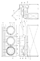
図1は、この発明の一実施の形態によるリフロー装置の全体の正面図、平面図、断面図である。リフロー装置は、一列に配された3個のチャンバ(ゾーン)1,2および3を有する。各チャンバ間は、隔壁で区切られ、隔壁に被加熱物としてのウエハWの搬送に必要な開口が形成される。
<1. First Embodiment>
"Outline of reflow equipment"
FIG. 1 is a front view, a plan view, and a cross-sectional view of an entire reflow apparatus according to an embodiment of the present invention. The reflow apparatus has three chambers (zones) 1, 2 and 3 arranged in a line. The chambers are separated by a partition, and an opening necessary for transporting the wafer W as an object to be heated is formed in the partition.
チャンバ1は、搬入/搬出用のチャンバである。チャンバ1から搬送治具に取付けられたウエハWが搬入され、リフロー処理後のウエハWがチャンバ1から搬出される。ウエハWは、例えば厚みが0.5mm〜1.5mm、直径が120mm〜300mmの単結晶シリコンウエハである。ウエハに対してバンプを形成する処理、シリコンチップを導体にはんだ付けする処理、フリップチップを導体にはんだ付けする処理等がリフロー装置によってなされる。ウエハWが薄いので、後述するように、ウエハWが搬送治具によって保持されている。チャンバ1の上方の筐体部分4が開閉自在とされている。
The chamber 1 is a loading / unloading chamber. The wafer W attached to the transfer jig is loaded from the chamber 1 and the wafer W after the reflow process is unloaded from the chamber 1. The wafer W is a single crystal silicon wafer having a thickness of 0.5 mm to 1.5 mm and a diameter of 120 mm to 300 mm, for example. A process for forming bumps on a wafer, a process for soldering a silicon chip to a conductor, a process for soldering a flip chip to a conductor, and the like are performed by a reflow apparatus. Since the wafer W is thin, the wafer W is held by a transfer jig as will be described later. The
治具に保持されたウエハWは、ループ状のアーム5に載置される。アーム5が水平方向搬送機構6によって搬送されることによって、ウエハWが搬送される。水平方向搬送機構6は、例えばボールねじによって構成される。図1では、各チャンバにウエハWが位置している状態が示されているが、ウエハWは、チャンバ1からチャンバ2、チャンバ3と順次送られ、チャンバ3において、加熱処理される。加熱後にチャンバ3からチャンバ2に送られ、冷却され、冷却後にチャンバ1において、治具に保持されたウエハWが外に取り出される。
The wafer W held by the jig is placed on the loop-
加熱ゾーンとしてのチャンバ3には、加熱プレート(以下、ヒータプレートと称する)7が設けられている。ヒータプレート7は、加熱面に密着または近接した治具に取り付けられたウエハWを加熱する。ヒータプレート7に多数の小穴が形成されており、治具(ウエハWが貼り付けられた微粘着フィルム)を吸引することによって、微粘着フィルムを加熱面に密着させるようになされている。ヒータプレート7は、例えば内部にヒータを有するものが使用される。ヒータプレート7は、固定されている。
The
チャンバ3には、外側への盛り上がりを有し、外周端面に弾性体を有する蓋8が昇降自在に設けられている。例えば蓋8は、開口が下側を向いた円筒状のものである。チャンバ3において、蓋8が微粘着フィルムに固定されたウエハWを覆うように、ウエハW上に置かれる。そして、蓋8の内側に形成された空間内の空気が図示しないが、真空ポンプ等によって排気される。そして、ほぼ真空雰囲気中で、加熱が行われ、はんだが溶融する。
The
チャンバ3においては、後述するように、加熱(昇温加熱)、プリヒート(予熱)および本加熱がなされる。本加熱は、ほぼ真空雰囲気中で行われる。加熱およびプリヒートは、不活性ガス例えば窒素雰囲気中で行われる。窒素置換を行ったり、真空にするために、蓋8には、図示しないが、複数のポートが設けられている。複数のポートに対して、バルブを介して窒素発生装置、真空ポンプ等が接続される。
In the
蓋8を昇降させるためのシリンダ9がチャンバ3に設けられている。ウエハWは、シリンダ10によって昇降される。シリンダ9および10は、空気圧を利用した昇降機構である。シリンダ10は、アーム5を昇降させることによって、ウエハWを昇降させる。したがって、シリンダ10は、アーム5と一体に水平方向に移動される。
A
チャンバ2において、本加熱が終了したウエハWが冷却される。チャンバ2には、冷却プレート11が設けられている。冷却されたウエハWがチャンバ2からチャンバ1に移送され、チャンバ1から外に取り出される。
In the
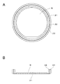
「搬送治具」
図2に示すように、ウエハWは、微粘着フィルム21の粘着面に貼り付けられる。ウエハWは、厚みが0.5mmのように薄いので、反りが発生し易い。微粘着フィルム21に対してウエハWを貼り付けることによって、ウエハWの反りを防止することができる。微粘着フィルム21は、高分子材料例えばPETの基材に対して微粘着力の粘着成分が塗布されたもので、はんだ付けの際に加わる熱に対して耐熱性を有する。微粘着フィルム21の粘着力は、ウエハWを処理終了後に外すのが容易であり、且つ搬送中および処理中にウエハWが剥がれない程度のものとされる。
"Transfer jig"
As shown in FIG. 2, the wafer W is attached to the adhesive surface of the slightly
微粘着フィルム21は、枠体としての内周リング22に張られ、内周リング22に対して外周リング23を嵌合させることによって、たるみなく内周リングに対して張ることができる。ウエハWが微粘着フィルム21の内面に貼り付けられる。ウエハWは、円形を有し、内周リング22に張られた微粘着フィルム21も円形を有する。内周リング22に張られた微粘着フィルム21の直径は、ウエハWよりやや大きくされる。内周リング22および外周リング23は、金属材料例えばステンレスからなる。
The slightly
図3に示すように、多数の小穴24が形成され、小穴24を通じてウエハWが吸着される微粘着フィルム21’を使用しても良い。小穴24の形成位置は、ヒータプレート7に形成されている吸引用の小穴の形成位置と一致される。一致させるために、位置決め機構が付加される。または、小穴24の径がヒータプレート7に形成されている小穴の径より大きいものとされ、位置ずれの影響を受けないようにしても良い。小穴24が形成された微粘着フィルム21’を使用する時には、ヒータプレート7側から真空引きを行う必要がある。
As shown in FIG. 3, a slightly
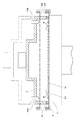
「加熱を行うチャンバの構成」
図4において、二点鎖線で示すように、搬送治具(微粘着フィルム21、内周リング22および外周リング23)に取り付けられたウエハWがチャンバ3内に搬送される。ウエハWがシリンダ10によって下降され、ヒータプレート7側からの吸引によって微粘着フィルム21がヒータプレート7の加熱面に対して密着される。
“Structure of chamber for heating”
In FIG. 4, as indicated by a two-dot chain line, the wafer W attached to the transfer jig (the slightly
さらに、シリンダ9によって蓋8が下降され、蓋8の端面に設けられた、耐熱性を有する弾性体41の端面によって、微粘着フィルム21が加熱面に対して押し付けられる。
ウエハWの外周位置と内周リング22の内側の位置との間に、微粘着フィルム21が露出する領域が形成されており、弾性体41の端面が露出している微粘着フィルム21に対して押し当てられる。さらに、弾性体41を有することによって、高さ方向に多少の機械的寸法誤差が存在していても、弾性体41と微粘着フィルム21の粘着面とが密に接触することができる。
Further, the
A region where the slightly
このように、蓋8の内側に気密な空間が形成される。蓋8には、ポート42aおよび42bが設けられている。各ポートには、配管が接続され、ポートまたは配管に対してバルブが設けられている。後述するように、蓋8の内側の空間の大気が不活性ガス(窒素)に置換される。さらに、蓋8の内側の空間が排気され、ほぼ真空雰囲気とされる。
Thus, an airtight space is formed inside the
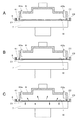
「リフロー処理」
上述したチャンバ3がリフロー時の温度プロファイルにしたがってウエハWの温度を制御する。図5に温度プロファイルの例の概略を示す。横軸が時間であり、縦軸がウエハWの表面温度である。最初の区間が加熱によって温度が上昇する昇温部R1であり、次の区間が温度がほぼ一定のプリヒート(予熱)部R2であり、次の区間が本加熱部R3であり、最後の区間が冷却部R4である。温度プロファイルは、図5において、実線で示すプロファイル51が代表的なものである。破線で示すプロファイル52、破線で示すプロファイル53に対してもこの発明を適用できる。
"Reflow processing"
The
昇温部R1は、常温からプリヒート部R2(例えば150°C〜170°C)までウエハWを加熱する期間である。プリヒート部R2は、等温加熱を行い、ウエハWの加熱ムラをなくすための期間である。本加熱部R3(例えばピーク温度で230°C〜250°C)は、はんだ例えば鉛フリーはんだが溶融し、接合またはバンプ形成が完成する期間である。R1〜R3の加熱処理がチャンバ3においてなされる。最後の冷却部R4は、急速にウエハWを冷却する期間である。ウエハWがチャンバ2において冷却プレート11によって冷却される。
The temperature raising portion R1 is a period in which the wafer W is heated from room temperature to a preheating portion R2 (for example, 150 ° C. to 170 ° C.). The preheating portion R2 is a period for performing isothermal heating to eliminate heating unevenness of the wafer W. The main heating portion R3 (for example, 230 ° C. to 250 ° C. at the peak temperature) is a period in which solder, for example, lead-free solder is melted and bonding or bump formation is completed. The heat treatment of R1 to R3 is performed in the
昇温部R1において、図6Aに示すように、窒素により置換された蓋8内の空間において、微粘着フィルム21がヒータプレート7の加熱面に密着され、ワークWが加熱される。加熱面への密着のために、ヒータプレート側から吸引を行っても良いが、シリンダ9によって蓋8の端面を加熱面に押し付けるのみでも良い。
In the temperature raising portion R1, as shown in FIG. 6A, in the space in the
プリヒート部R2において、図6Bに示すように、蓋8内の空間の窒素雰囲気を保持するように、蓋8の開口を微粘着フィルム21によって覆う状態を保持して、蓋8および微粘着フィルムに貼り付けられたウエハWが上方に移動される。図6Bに示す状態は、シリンダ9および10を制御することによって実現できる。さらに、微粘着フィルム21とヒータプレート7の加熱面とを離す距離は、温度プロファイル上のプリヒート部R2の温度変化が生じるように選定される。プリヒート部R2の温度変化は、やや上昇する程度であるため、ヒータプレート7の加熱面と微粘着フィルム21との間を離間させる。
In the preheating part R2, as shown in FIG. 6B, the
本加熱部R3において、図6Cに示すように、蓋8内の空間の窒素がポート42a、42bの一方または両方を通じて吸引されてほぼ真空雰囲気とされると共に、微粘着フィルム21がヒータプレート7側の吸引によって、加熱面に密着される。ヒータプレート7は、伝導熱によりウエハWを加熱するために、微粘着フィルム21と加熱面とを密着させることが必要とされる。図3に示すような多数の小穴24が形成されている微粘着フィルム21’を使用する時には、ヒータプレート7側からの吸引によって、真空雰囲気を形成できると共に、微粘着フィルム24’を加熱面に密着させることができる。
In the main heating portion R3, as shown in FIG. 6C, nitrogen in the space in the
<2.変形例>
この発明は、上述したこの発明の実施の形態に限定されるものでは無く、この発明の要旨を逸脱しない範囲内で様々な変形や応用が可能である。例えば、チャンバ(ゾーン)を増加させて、入口側搬送部と出口側搬送部とを別に設けても良い。さらに、不活性ガスの雰囲気での加熱を受け持つチャンバと、真空雰囲気での加熱を受け持つチャンバとを別々に設けても良い。
<2. Modification>
The present invention is not limited to the above-described embodiment of the present invention, and various modifications and applications can be made without departing from the gist of the present invention. For example, the number of chambers (zones) may be increased, and the entrance side transport unit and the exit side transport unit may be provided separately. Further, a chamber responsible for heating in an inert gas atmosphere and a chamber responsible for heating in a vacuum atmosphere may be provided separately.
W・・・ウエハ
1、2、3・・・チャンバ
7・・・ヒータプレート
8・・・ヒータプレート
9、10・・・シリンダ
11・・・冷却プレート
21、21’・・・微粘着フィルム
22・・・内周リング
23・・・外周リング
24・・・小穴
41・・・弾性体
W ...
Claims (4)
外周端面が弾性を有する蓋と、
被加熱物と上記蓋とをそれぞれ昇降させる昇降部と、
上記被加熱物が降下する位置に配された加熱プレートとを備え、
上記被加熱物は、
枠体の端面に、開口を覆うように取り付けられた耐熱性のある微粘着フィルムと、
上記微粘着フィルムの粘着面に貼り付けられたワークとからなり、
上記被加熱物が上記昇降部によって下降されることによって、上記微粘着フィルムが上記加熱プレートに対して密着され、
上記蓋が上記昇降部によって下降されることによって、上記ワークの外周位置と、上記枠体の内周位置との間の領域に対して、上記蓋の外周端面が密着され、
上記蓋の内側に形成される空間内を減圧することによって、ほぼ真空雰囲気において加熱工程が行われるリフローはんだ付装置。 A reflow soldering apparatus for performing soldering by heating an object to be heated in a substantially reduced pressure atmosphere,
A lid having an elastic peripheral end surface;
An elevating part for elevating and lowering the object to be heated and the lid;
A heating plate disposed at a position where the object to be heated descends,
The heated object is
A heat-resistant slightly adhesive film attached to the end face of the frame so as to cover the opening;
It consists of a work affixed to the adhesive surface of the above slightly adhesive film,
When the object to be heated is lowered by the elevating unit, the slightly adhesive film is in close contact with the heating plate,
When the lid is lowered by the elevating part, the outer peripheral end surface of the lid is brought into close contact with the region between the outer peripheral position of the workpiece and the inner peripheral position of the frame,
A reflow soldering apparatus in which a heating process is performed in a substantially vacuum atmosphere by reducing the pressure in a space formed inside the lid.
Priority Applications (1)
| Application Number | Priority Date | Filing Date | Title |
|---|---|---|---|
| JP2009138709A JP2010287635A (en) | 2009-06-09 | 2009-06-09 | Reflow device |
Applications Claiming Priority (1)
| Application Number | Priority Date | Filing Date | Title |
|---|---|---|---|
| JP2009138709A JP2010287635A (en) | 2009-06-09 | 2009-06-09 | Reflow device |
Publications (1)
| Publication Number | Publication Date |
|---|---|
| JP2010287635A true JP2010287635A (en) | 2010-12-24 |
Family
ID=43543145
Family Applications (1)
| Application Number | Title | Priority Date | Filing Date |
|---|---|---|---|
| JP2009138709A Pending JP2010287635A (en) | 2009-06-09 | 2009-06-09 | Reflow device |
Country Status (1)
| Country | Link |
|---|---|
| JP (1) | JP2010287635A (en) |
Cited By (7)
| Publication number | Priority date | Publication date | Assignee | Title |
|---|---|---|---|---|
| CN103600152A (en) * | 2013-11-15 | 2014-02-26 | 合肥科烨电物理设备制造有限公司 | Pressure soldering device used under protection of inert gas in furnace and welding method |
| KR101491992B1 (en) * | 2013-01-08 | 2015-02-10 | (주)에스티아이 | Continuous treatment method of semiconductor wafer |
| JP2020069480A (en) * | 2018-10-29 | 2020-05-07 | 株式会社タムラ製作所 | Transport heating apparatus |
| JP2021507812A (en) * | 2017-12-29 | 2021-02-25 | シャンドン ツァイジュー エレクトロニック テクノロジー カンパニー リミテッド | Vacuum welding furnace for a wide range |
| JP2021508602A (en) * | 2017-12-29 | 2021-03-11 | シャンドン ツァイジュー エレクトロニック テクノロジー カンパニー リミテッド | Vacuum welding furnace and welding method |
| US11315809B2 (en) | 2020-08-03 | 2022-04-26 | Japan Aviation Electronics Industry, Limited | Device and forming method of device |
| US11469150B2 (en) | 2020-03-18 | 2022-10-11 | Japan Aviation Electronics Industry, Limited | Device and forming method of device |
-
2009
- 2009-06-09 JP JP2009138709A patent/JP2010287635A/en active Pending
Cited By (11)
| Publication number | Priority date | Publication date | Assignee | Title |
|---|---|---|---|---|
| KR101491992B1 (en) * | 2013-01-08 | 2015-02-10 | (주)에스티아이 | Continuous treatment method of semiconductor wafer |
| CN103600152A (en) * | 2013-11-15 | 2014-02-26 | 合肥科烨电物理设备制造有限公司 | Pressure soldering device used under protection of inert gas in furnace and welding method |
| CN103600152B (en) * | 2013-11-15 | 2015-09-30 | 合肥科烨电物理设备制造有限公司 | A kind of for inert gas shielding downforce soldering apparatus in stove |
| JP2021507812A (en) * | 2017-12-29 | 2021-02-25 | シャンドン ツァイジュー エレクトロニック テクノロジー カンパニー リミテッド | Vacuum welding furnace for a wide range |
| JP2021508602A (en) * | 2017-12-29 | 2021-03-11 | シャンドン ツァイジュー エレクトロニック テクノロジー カンパニー リミテッド | Vacuum welding furnace and welding method |
| JP7127132B2 (en) | 2017-12-29 | 2022-08-29 | シャンドン ツァイジュー エレクトロニック テクノロジー カンパニー リミテッド | Vacuum welding furnace and welding method |
| JP7181297B2 (en) | 2017-12-29 | 2022-11-30 | シャンドン ツァイジュー エレクトロニック テクノロジー カンパニー リミテッド | Wide-ranging vacuum welding furnace |
| JP2020069480A (en) * | 2018-10-29 | 2020-05-07 | 株式会社タムラ製作所 | Transport heating apparatus |
| JP7169161B2 (en) | 2018-10-29 | 2022-11-10 | 株式会社タムラ製作所 | Conveyor heating device |
| US11469150B2 (en) | 2020-03-18 | 2022-10-11 | Japan Aviation Electronics Industry, Limited | Device and forming method of device |
| US11315809B2 (en) | 2020-08-03 | 2022-04-26 | Japan Aviation Electronics Industry, Limited | Device and forming method of device |
Similar Documents
| Publication | Publication Date | Title |
|---|---|---|
| KR101915441B1 (en) | Bonding method and computer storage medium and bonding apparatus and bonding system | |
| JP2010287635A (en) | Reflow device | |
| CN110416142B (en) | Bonding device, bonding system, and bonding method | |
| JP4781802B2 (en) | Support plate laminating means and laminating apparatus, and support plate laminating method | |
| JP5547147B2 (en) | Joining apparatus, joining system, joining method, program, and computer storage medium | |
| JP5421967B2 (en) | Joining method, program, computer storage medium, and joining system | |
| JP6614933B2 (en) | Substrate mounting mechanism and substrate processing apparatus | |
| CN108807193B (en) | Bonding device and bonding method | |
| CN110998813B (en) | Hot wall soldering flux-free solder ball treatment device | |
| JP5314607B2 (en) | Joining apparatus, joining method, program, and computer storage medium | |
| JP5406257B2 (en) | Joining method, program, computer storage medium, and joining system | |
| KR20120091323A (en) | Substrate processing device, substrate processing method, program, and computer recording medium | |
| JP5528405B2 (en) | Joining method, program, computer storage medium, and joining system | |
| JP5905509B2 (en) | Joining apparatus, joining system, joining method, program, and computer storage medium | |
| WO2013046991A1 (en) | Three-dimensional mounting device | |
| JP5427856B2 (en) | Joining method, program, computer storage medium, and joining system | |
| JP6535828B1 (en) | Substrate processing equipment | |
| JP5869960B2 (en) | Joining system, joining method, program, and computer storage medium | |
| JP5905407B2 (en) | Sheet peeling apparatus, bonding system, peeling system, sheet peeling method, program, and computer storage medium | |
| JP5552466B2 (en) | Joining method, program, computer storage medium, and joining system | |
| TW202312291A (en) | Manufacturing method of semiconductor products, workpiece integration devices, film laminate, and semiconductor products | |
| JP4587881B2 (en) | Resin sealing device | |
| JP2016129197A (en) | Bonding device, bonding system, bonding method, program and computer storage medium |