RU2750503C1 - Method for producing a multilayer thin-film heterostructure with a given value of specific surface resistance - Google Patents
Method for producing a multilayer thin-film heterostructure with a given value of specific surface resistance Download PDFInfo
- Publication number
- RU2750503C1 RU2750503C1 RU2020140228A RU2020140228A RU2750503C1 RU 2750503 C1 RU2750503 C1 RU 2750503C1 RU 2020140228 A RU2020140228 A RU 2020140228A RU 2020140228 A RU2020140228 A RU 2020140228A RU 2750503 C1 RU2750503 C1 RU 2750503C1
- Authority
- RU
- Russia
- Prior art keywords
- tcr
- metal
- spraying
- film
- specific surface
- Prior art date
Links
- 239000010409 thin film Substances 0.000 title claims abstract description 39
- 238000004519 manufacturing process Methods 0.000 title claims abstract description 6
- 229910052751 metal Inorganic materials 0.000 claims abstract description 82
- 239000002184 metal Substances 0.000 claims abstract description 82
- 238000005507 spraying Methods 0.000 claims abstract description 58
- 239000000463 material Substances 0.000 claims abstract description 38
- 239000010408 film Substances 0.000 claims abstract description 27
- PXHVJJICTQNCMI-UHFFFAOYSA-N Nickel Chemical compound [Ni] PXHVJJICTQNCMI-UHFFFAOYSA-N 0.000 claims abstract description 23
- 230000008021 deposition Effects 0.000 claims abstract description 20
- 239000010936 titanium Substances 0.000 claims abstract description 17
- 239000000758 substrate Substances 0.000 claims abstract description 14
- 230000015572 biosynthetic process Effects 0.000 claims abstract description 12
- 239000011651 chromium Substances 0.000 claims abstract description 12
- 229910052759 nickel Inorganic materials 0.000 claims abstract description 9
- 229910052719 titanium Inorganic materials 0.000 claims abstract description 9
- RTAQQCXQSZGOHL-UHFFFAOYSA-N Titanium Chemical compound [Ti] RTAQQCXQSZGOHL-UHFFFAOYSA-N 0.000 claims abstract description 7
- 229910052804 chromium Inorganic materials 0.000 claims abstract description 7
- VYZAMTAEIAYCRO-UHFFFAOYSA-N Chromium Chemical compound [Cr] VYZAMTAEIAYCRO-UHFFFAOYSA-N 0.000 claims abstract description 6
- XEEYBQQBJWHFJM-UHFFFAOYSA-N Iron Chemical compound [Fe] XEEYBQQBJWHFJM-UHFFFAOYSA-N 0.000 claims abstract description 6
- 239000010941 cobalt Substances 0.000 claims abstract description 5
- 229910017052 cobalt Inorganic materials 0.000 claims abstract description 5
- GUTLYIVDDKVIGB-UHFFFAOYSA-N cobalt atom Chemical compound [Co] GUTLYIVDDKVIGB-UHFFFAOYSA-N 0.000 claims abstract description 5
- 239000003446 ligand Substances 0.000 claims abstract description 5
- LEONUFNNVUYDNQ-UHFFFAOYSA-N vanadium atom Chemical compound [V] LEONUFNNVUYDNQ-UHFFFAOYSA-N 0.000 claims abstract description 5
- 239000004020 conductor Substances 0.000 claims abstract description 3
- 238000005530 etching Methods 0.000 claims abstract description 3
- 238000000206 photolithography Methods 0.000 claims abstract description 3
- 239000002052 molecular layer Substances 0.000 claims description 34
- 238000000151 deposition Methods 0.000 claims description 19
- 239000002120 nanofilm Substances 0.000 claims description 12
- 238000001755 magnetron sputter deposition Methods 0.000 claims description 9
- 238000005137 deposition process Methods 0.000 claims description 2
- 238000004544 sputter deposition Methods 0.000 claims description 2
- 238000000034 method Methods 0.000 abstract description 12
- 230000014509 gene expression Effects 0.000 abstract description 8
- 238000005516 engineering process Methods 0.000 abstract description 7
- 230000000694 effects Effects 0.000 abstract description 2
- 239000000126 substance Substances 0.000 abstract description 2
- 239000010410 layer Substances 0.000 description 42
- 150000002739 metals Chemical class 0.000 description 13
- 238000012544 monitoring process Methods 0.000 description 6
- 238000013461 design Methods 0.000 description 4
- XKRFYHLGVUSROY-UHFFFAOYSA-N Argon Chemical compound [Ar] XKRFYHLGVUSROY-UHFFFAOYSA-N 0.000 description 2
- 238000004458 analytical method Methods 0.000 description 2
- 239000000203 mixture Substances 0.000 description 2
- 238000000427 thin-film deposition Methods 0.000 description 2
- 239000000956 alloy Substances 0.000 description 1
- 229910045601 alloy Inorganic materials 0.000 description 1
- 238000013459 approach Methods 0.000 description 1
- 229910052786 argon Inorganic materials 0.000 description 1
- 238000009530 blood pressure measurement Methods 0.000 description 1
- 230000000368 destabilizing effect Effects 0.000 description 1
- 238000010586 diagram Methods 0.000 description 1
- 239000002828 fuel tank Substances 0.000 description 1
- 239000007789 gas Substances 0.000 description 1
- 230000036039 immunity Effects 0.000 description 1
- 229910052742 iron Inorganic materials 0.000 description 1
- 230000003647 oxidation Effects 0.000 description 1
- 238000007254 oxidation reaction Methods 0.000 description 1
- 230000035945 sensitivity Effects 0.000 description 1
- 239000002356 single layer Substances 0.000 description 1
- 229910052715 tantalum Inorganic materials 0.000 description 1
- GUVRBAGPIYLISA-UHFFFAOYSA-N tantalum atom Chemical compound [Ta] GUVRBAGPIYLISA-UHFFFAOYSA-N 0.000 description 1
- WFKWXMTUELFFGS-UHFFFAOYSA-N tungsten Chemical compound [W] WFKWXMTUELFFGS-UHFFFAOYSA-N 0.000 description 1
- 229910052721 tungsten Inorganic materials 0.000 description 1
- 239000010937 tungsten Substances 0.000 description 1
- 229910052720 vanadium Inorganic materials 0.000 description 1
Images
Classifications
-
- H—ELECTRICITY
- H01—ELECTRIC ELEMENTS
- H01C—RESISTORS
- H01C17/00—Apparatus or processes specially adapted for manufacturing resistors
- H01C17/06—Apparatus or processes specially adapted for manufacturing resistors adapted for coating resistive material on a base
Landscapes
- Engineering & Computer Science (AREA)
- Manufacturing & Machinery (AREA)
- Microelectronics & Electronic Packaging (AREA)
- Measurement Of Length, Angles, Or The Like Using Electric Or Magnetic Means (AREA)
- Physical Vapour Deposition (AREA)
Abstract
Description
Изобретение относится к области электронной техники, а именно к средствам измерения, в которых применяют тонкопленочные тензорезисторы на металлической подложке, изготовляемые с применением технологии тонких пленок.The invention relates to the field of electronic engineering, namely to measuring instruments that use thin-film strain gauges on a metal substrate, manufactured using thin-film technology.
При работе тонкопленочных тензорезисторных датчиков давления в системах управления и контроля изделий для особо жестких условий эксплуатации (ракетные и авиационные двигатели, турбонасосные агрегаты, топливные баки ракет-носителей и космических аппаратов) возникает ряд дестабилизирующих факторов, которые приводят к искажению информации о фактическом давлении рабочей среды в критических для надежности и безопасности зонах двигателей и других агрегатов на борту изделия.During the operation of thin-film strain gauge pressure sensors in control and monitoring systems of products for particularly harsh operating conditions (rocket and aircraft engines, turbopump units, fuel tanks of launch vehicles and spacecraft), a number of destabilizing factors arise that lead to distortion of information about the actual pressure of the working environment in areas critical for reliability and safety of engines and other units on board the product.
Известна конструкция тензометрического датчика давления, где в качестве тензорезисторов применяют многослойную тонкопленочную гетероструктуру, в которой первый пакет слоев с многослойной (5 слоев) кристаллической гетероструктурой состоит из чередующихся слоев хрома и вольфрама с отрицательным ТКС и второй слой - из аморфной тонкой пленки тантала с положительным ТКС. В патенте предлагается формула, позволяющая вычислять величину ТКС тензорезистора исходя из сопротивления чередующихся слоев [USA патент 6,614,342 G01L 1/22, G01B 7/16, G01L 9/00, G01L 1/20, G01L 001/22, опубликован 02.09.2003].The design of a strain gauge pressure sensor is known, where a multilayer thin-film heterostructure is used as strain gauges, in which the first layer of layers with a multilayer (5 layers) crystalline heterostructure consists of alternating layers of chromium and tungsten with negative TCR and the second layer is made of an amorphous thin film of tantalum with a positive TCR ... The patent proposes a formula that allows you to calculate the TCR value of the strain gauge based on the resistance of alternating layers [USA patent 6,614,342 G01L 1/22, G01B 7/16, G01L 9/00, G01L 1/20, G01L 001/22, published 02.09.2003].
Недостатком данной конструкции тензометрического датчика давления является низкая темературная стабильностиь тензорезистора обусловленная высоким начальным разбалансом тензомоста за счет окисления материалов тензорезистора от воздействия температуры и времени.The disadvantage of this design of the strain gauge pressure sensor is the low temperature stability of the strain gauge due to the high initial imbalance of the strain gage due to the oxidation of the strain gauge materials from the effects of temperature and time.
Известен материал металлопленочного аморфного резистивного слоя (на основе сплавов магнитных 3d-металлов, имеющих химический состав, включающий от 10 до 90 ат.% одного или двух элементов из группы металлов: железо (Fe), никель (Ni), кобальт (Со) и от 90 до 10 ат.% одного из металлов лигандов: ванадий (V), хром (Cr), титан (Ti) [RU патент 2280905, G11B 5/84, Н01С 17/00, опубликован 27.07.2006] и способ получения резистивного слоя на его основе с применением технологии послойного ионно-плазменного (магнетронного) распыления мишений из комбинации вышеуказанных чистых металлов в среде рабочего газа аргона при давлении 2×10⁻¹ Па [RU патент 2122243, G11B 5/84, опубликован 20.11.1998].Known material for a metal-film amorphous resistive layer (based on alloys of magnetic 3d-metals having a chemical composition comprising from 10 to 90 at.% Of one or two elements from the group of metals: iron (Fe), nickel (Ni), cobalt (Co) and from 90 to 10 at.% of one of the ligand metals: vanadium (V), chromium (Cr), titanium (Ti) [RU patent 2280905,
Недостатком данного материала из композиции металлов Fe, Ni, Со и V, Cr, Ti и способа получения из них тонкопленочных резисторов является нестабильность начального выходного сигнала датчика связанного с высоким уровнем удельного поверхностного сопротивления (200-900 мкОм см) при больших значениях ТКС (1×10⁻⁴ 1/°С).The disadvantage of this material from the composition of metals Fe, Ni, Co and V, Cr, Ti and the method of obtaining thin-film resistors from them is the instability of the initial output signal of the sensor associated with a high level of specific surface resistance (200-900 μOhm cm) at high TCR values (1 × 10 -4 1 / ° C).
Наиболее близким к заявляемому решению является способ изготовления нано- и микроразмерной системы датчика физических величин с заданным положительным температурным коэффициентом сопротивления резистивных элементов, заключающийся в получении многослойной тонкопленочной гетероструктуры с тензорезисторами из чередующихся слоев никеля и титана методом магнетронного распыления. При этом плотности токов магнетронного разряда JTi и JNi на мишенях из Ti и Ni определяются из соотношения:The closest to the claimed solution is a method of manufacturing a nano- and micro-size sensor system of physical quantities with a given positive temperature coefficient of resistance of resistive elements, which consists in obtaining a multilayer thin-film heterostructure with strain gauges from alternating layers of nickel and titanium by the method of magnetron sputtering. In this case, the current densities of the magnetron discharge J Ti and J Ni on the Ti and Ni targets are determined from the relation:
где jTi и jNi - плотности токов магнетронного разряда на мишенях из титана (Ti) и никеля (Ni) соответственно;where j Ti and j Ni are the current densities of the magnetron discharge on titanium (Ti) and nickel (Ni) targets, respectively;
α - значение ТКС тензорезисторов в интервале от 5×10⁻⁵ °С-1 до 1×10⁻³ °С-1, при этом значение плотности тока JTi на мишени Ti выбирают в интервале от 10-3 до 5×10⁻³ А/см2 [RU патент 2554083, Н01С 17/06, опубликован 27.06.2015].α is the TCR value of strain gauges in the range from 5 × 10 -5 ° С -1 to 1 × 10 -3 ° С -1 , while the value of the current density J Ti on the Ti target is selected in the range from 10 -3 to 5 × 10 - 3 A / cm 2 [RU patent 2554083, Н01С 17/06, published on June 27, 2015].
Недостатком данного способа получения многослойной тонкопленочной гетероструктуры является низкая величина удельного поверхностного сопротивления получаемой тонкой резистивной пленки в диапазоне от 16 до 18 Ом/кв, что не позволяет формировать из нее тензосхемы с высокой температурной стабильностью начального выходного сигнала и применять эти тензосхемы в чувствительных элементах датчиков давления для систем управления и контроля изделий в особо жестких условиях эксплуатации.The disadvantage of this method of obtaining a multilayer thin-film heterostructure is the low value of the specific surface resistance of the resulting thin resistive film in the range from 16 to 18 Ohm / sq, which does not allow forming from it strain gauges with a high temperature stability of the initial output signal and using these strain gauges in sensitive elements of pressure sensors for control and monitoring systems of products in especially harsh operating conditions.
Целью изобретения является повышение температурной стабильности тонкопленочных тензорезисторов для микроэлектромеханических датчиков абсолютного и избыточного давления в расширенном диапазоне рабочих температур, обусловленной получением тонкопленочной нано- и микроразмерной системы с заданным положительным минимальным температурным коэффициентом сопротивления (ТКС).The aim of the invention is to increase the temperature stability of thin-film strain gauges for microelectromechanical absolute and gauge pressure sensors in an extended operating temperature range due to the production of a thin-film nano- and micro-sized system with a given positive minimum temperature coefficient of resistance (TCR).
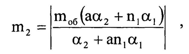
Поставленная цель достигается тем, что в способе изготовления тонкопленочной нано- и микроразмерной системы датчика физических величин с заданным положительным температурным коэффициентом сопротивления (ТКС) резистивных элементов, заключающемся в том, что на планарной стороне твердотельной подложки методами вакуумного распыления образуют гетерогенную структуру из нано- и микроразмерных пленок материалов, содержащую тонкопленочные диэлектрические, резистивные и контактные слои, после чего с использованием фотолитографии и травления формируют резистивные элементы (тензорезисторы, терморезисторы), контактные проводники и контактные площадки к ним, при этом, резистивный слой формируют методом магнетронного распыления в вакуумной камере, одновременно из двух раздельных источников, согласно изобретения, формирование резистивных слоев методом магнетронного распыления в вакуумной камере проводят с использованием одного из элементов группы металлов: железо (Fe), никель (Ni), кобальт (Со) с одной мишени и одного из металлических лигандов: ванадий (V), хром (Cr), титан (Ti) с другой мишени, при этом путем изменения соотношения компонентов в гетероструктуре по процентному содержанию от 10% до 90% формируют требуемую величину удельного поверхностного сопротивления резистивной пленки и момент окончания процесса напыления многослойной гетероструктуры контролируют по сопротивлению свидетеля, расположенного на карусели подложек, а количество циклов совместного напыления слоев гетероструктуры m2 определяют по формуле:This goal is achieved by the fact that in the method of manufacturing a thin-film nano- and micro-sized system of a sensor of physical quantities with a given positive temperature coefficient of resistance (TCR) of resistive elements, which consists in the fact that a heterogeneous structure of nano- and micro-sized films of materials containing thin-film dielectric, resistive and contact layers, after which, using photolithography and etching, resistive elements (strain gauges, thermistors), contact conductors and contact pads to them are formed, while the resistive layer is formed by magnetron sputtering in a vacuum chamber, simultaneously from two separate sources, according to the invention, the formation of resistive layers by magnetron sputtering in a vacuum chamber is carried out using one of the elements of the metal group: iron (Fe), nickel (Ni), cobalt (Co) with one th target and one of the metal ligands: vanadium (V), chromium (Cr), titanium (Ti) from another target, while changing the ratio of components in the heterostructure in percentage from 10% to 90% form the required specific surface resistance of the resistive films and the end of the deposition process of the multilayer heterostructure are controlled by the resistance of the witness located on the carousel of substrates, and the number of cycles of joint deposition of heterostructure layers m 2 is determined by the formula:
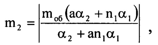
где mоб - общее количество циклов напыления, необходимое для обеспечения требуемой величины удельного поверхностного сопротивления резистивного слоя RS;where m about - the total number of spraying cycles required to ensure the required value of the specific surface resistance of the resistive layer R S ;
а - коэффициент характеризующий соотношение циклов напыления m3 и m1 отдельных нанослоев только из материала с положительным ТКС;a - coefficient characterizing the ratio of the spraying cycles m 3 and m 1 of individual nanolayers only from a material with a positive TCR;
m3 - количество циклов напыления только нанослоя из резистивного материала с положительным ТКС;m 3 is the number of cycles of spraying only a nanolayer of a resistive material with a positive TCR;
n1 - коэффициент соотношения приращения удельного поверхностного сопротивления пленки второго металла Δρs2 за один цикл напыления и приращения удельного поверхностного сопротивления пленки первого металла Δρs1 за один цикл напыления определяют по формуле n1=Δρs2/Δρs1;n 1 - coefficient of the ratio of the increment of the specific surface resistance of the film of the second metal Δρ s2 for one cycle of spraying and the increment of the specific surface resistance of the film of the first metal Δρ s1 during one cycle of spraying is determined by the formula n 1 = Δρ s2 / Δρ s1 ;
α1 - ТКС нанопленки из первого металла;α 1 - TCR nanofilm from the first metal;
α2 - ТКС нанопленки из второго металла,α 2 - TCR nanofilm from the second metal,
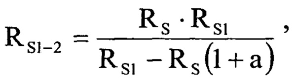
расчетная величина удельного поверхностного сопротивления RS1-2 отдельного резистивного слоя с положительным ТКС определяют из величин удельного поверхностного сопротивления взаимочередующихся нанослоев по формуле:The calculated value of the specific surface resistance R S1-2 of a separate resistive layer with a positive TCR is determined from the values of the specific surface resistance of alternating nanolayers by the formula:
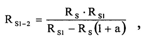
где а - коэффициент характеризующий соотношение циклов напыления m3 и m1 отдельных нанослоев только из материала с положительным ТКС;where a is the coefficient characterizing the ratio of the spraying cycles m 3 and m 1 of individual nanolayers only from a material with a positive TCR;
RS1 - удельное поверхностное сопротивление нанослоя из первого металла;R S1 - surface resistivity of the first metal nanolayer;
RS - общее удельное поверхностное сопротивление многослойной гетероструктуры,R S is the total specific surface resistance of the multilayer heterostructure,
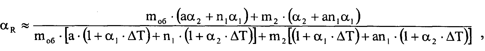
условием возможности управления величиной ТКС многслойной резистивной гетероструктуры является следующее неравенство |а α2|<|n1 α1|, ТКС (αR) для многослойного тонкопленочного тензорезистора со структурой резистивного слоя из взаимочередующихся нанослоев и отдельным слоем из материала с положительным ТКС определяют по формуле:The condition for the possibility of controlling the value of the TCR of a multilayer resistive heterostructure is the following inequality | а α 2 | <| n 1 α 1 |, TCR (α R ) for a multilayer thin-film strain gauge with a resistive layer structure of alternating nanolayers and a separate layer of material with a positive TCR is determined by formula:
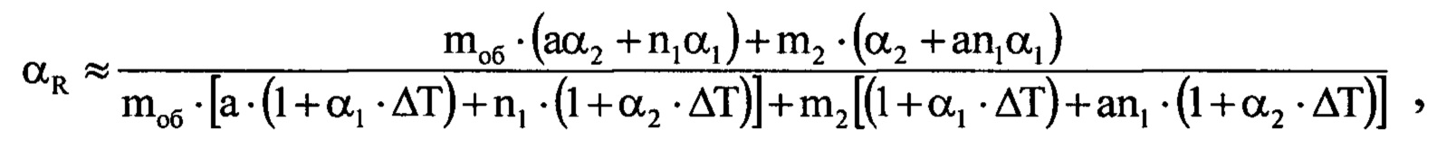
где mоб - общее количество циклов напыления, необходимое для обеспечения требуемой величины удельного поверхностного сопротивления резистивного слоя RS;where m about - the total number of spraying cycles required to ensure the required value of the specific surface resistance of the resistive layer R S ;
m2 - количество циклов совместного напыления взаимочередующихся нанослоев материалов с противоположными по знаку ТКС;m 2 - the number of cycles of joint spraying of alternating nanolayers of materials with opposite signs of TCS;
α1 - ТКС нанопленки из первого металла;α 1 - TCR nanofilm from the first metal;
α2 - ТКС нанопленки из второго металла;α 2 - TCR nanofilm from the second metal;
а - коэффициент характеризующий соотношение циклов напыления m3 и m1 отдельных нанослоев только из материала с положительным ТКС;a - coefficient characterizing the ratio of the spraying cycles m 3 and m 1 of individual nanolayers only from a material with a positive TCR;
n1 - коэффициент соотношения приращения удельного поверхностного сопротиления пленки второго металла Δρs2 за один цикл напыления и приращения удельного поверхностного сопротиления пленки первого металла Δρs1 за один цикл напыления определяют по формуле n1=Δρs2/Δρs1;n 1 - the ratio of the increment of the specific surface resistance of the film of the second metal Δρ s2 for one cycle of spraying and the increment of the specific surface resistance of the film of the first metal Δρ s1 for one cycle of spraying is determined by the formula n 1 = Δρ s2 / Δρ s1 ;
ΔT - диапазон температур замера ТКС,ΔT - temperature range for measuring TCR,
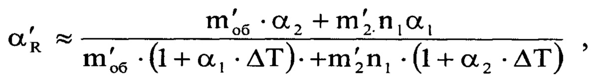
ТКС (α’R) для многослойного тонкопленочного тензорезистора со структурой резистивного слоя из взаимочередующихся нанослоев и отдельным слоем из материала с отрицательным ТКС определяют по формуле:TCR (α ' R ) for a multilayer thin-film strain gauge with the structure of a resistive layer of alternating nanolayers and a separate layer of a material with negative TCR is determined by the formula:
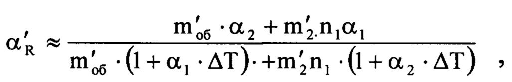
где m'об - общее количество циклов напыления, необходимое для обеспечения требуемой величины удельного поверхностного сопротивления резистивного слоя RS;where m ' about - the total number of spraying cycles required to ensure the required value of the specific surface resistance of the resistive layer R S ;
m'2 - количество циклов совместного напыления взаимочередующихся нанослоев материалов с противоположными по знаку ТКС;m ' 2 - the number of cycles of joint spraying of alternating nanolayers of materials with opposite signs of TCS;
α1 - ТКС нанопленки из первого металла;α 1 - TCR nanofilm from the first metal;
α2 - ТКС нанопленки из второго металла;α 2 - TCR nanofilm from the second metal;
n1 - коэффициент соотношения приращения удельного поверхностного сопротивления пленки второго металла Δρs2 за один цикл напыления и приращения удельного поверхностного сопротиления пленки первого металла Δρs1 за один цикл напыления определяют по формуле n1=Δρs2/Δρs1;n 1 is the ratio of the increment in the specific surface resistance of the film of the second metal Δρ s2 for one cycle of spraying and the increment in the specific surface resistance of the film of the first metal Δρ s1 during one cycle of spraying is determined by the formula n 1 = Δρ s2 / Δρ s1 ;
ΔT - диапазон температур замера ТКС.ΔT - temperature range for measuring TCR.
Многослойная тонкопленочная гетероструктура, полученная предлагаемым способом, позволяет сформировать удельное поверхностное сопротивление тонкопленочной гетероструктуры в диапазоне от 60 до 70 Ом/кв, что в свою очередь позволяет создать тензомост датчика давления с сопротивлением диагонали не менее 1,5 кОм. Эта конструктувная особенность тензомоста повышает помехоустойчивость и гарантированную чувствительность всей пространнственно разделенной системы измерений давления, включающей в себя измерительную цепь датчика и электронный преобразователь сигнала в общей телеметрической системе управления и контроля сложными техническими объектами.The multilayer thin-film heterostructure obtained by the proposed method makes it possible to form the specific surface resistance of the thin-film heterostructure in the range from 60 to 70 Ohm / sq, which in turn makes it possible to create a strain gauge pressure sensor with a diagonal resistance of at least 1.5 kOhm. This design feature of the strain bridge increases the noise immunity and guaranteed sensitivity of the entire spatially separated pressure measurement system, which includes the sensor measuring circuit and the electronic signal converter in the general telemetric control and monitoring system for complex technical objects.
Управление формированием многослойной гетероструктуры осуществляют путем использования технологии магнетронного распыления одного из элементов из группы металлов: железо (Fe), никель (Ni), кобальт (Со) с одной мишени и одного из металлов лигандов: ванадий (V), хром (Cr), титан (Ti) с другой мишени. Управление величиной удельного поверхностного сопротивления тонкой пленки осуществляют путем изменения соотношения компонентов многослойной гетероструктуры по процентному содержанию от 10% до 90% и с контролем окончания процесса напыления тонкой пленки по сопротивлению свидетеля на карусели подложек. Величину сопротивления свидетеля задают заранее, исходя из количества квадратов напыляемой пленки на свидетель и требуемой величины удельного поверхностного сопротивления создаваемой многослойной гетероструктуры. Процесс контроля осаждения многослойной гетероструктуры с помощью свидетеля на карусели подложек позволяет управлять величиной удельного поверхностного сопротивления создаваемой многослойной гетероструктуры и величиной ее ТКС.The formation of a multilayer heterostructure is controlled by using the technology of magnetron sputtering of one of the elements from the group of metals: iron (Fe), nickel (Ni), cobalt (Co) from one target and one of the ligand metals: vanadium (V), chromium (Cr), titanium (Ti) from another target. The value of the specific surface resistance of the thin film is controlled by changing the ratio of the components of the multilayer heterostructure by percentage from 10% to 90% and by monitoring the end of the thin film deposition process by the resistance of the witness on the carousel of substrates. The value of the resistance of the witness is set in advance, based on the number of squares of the sprayed film on the witness and the required value of the specific surface resistance of the created multilayer heterostructure. The process of monitoring the deposition of a multilayer heterostructure with the help of a witness on a carousel of substrates makes it possible to control the value of the specific surface resistance of the created multilayer heterostructure and the value of its TCR.
Необходимо отметить, что при общей толщине многослойной резистивной пленки порядка 80-130 нм каждый отдельный монослой будет иметь толщину менее 10 нм, то есть эти монослои правильнее будет называть нанослоями.It should be noted that with a total thickness of a multilayer resistive film of the order of 80-130 nm, each individual monolayer will have a thickness of less than 10 nm, that is, these monolayers will be more correctly called nanolayers.
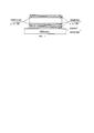
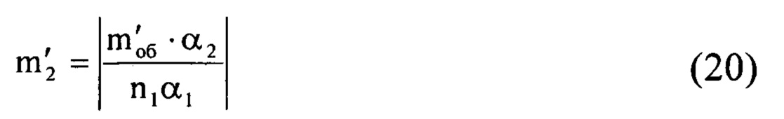
На фиг. 1 изображена структурная схема многослойной гетероструктуры тонкопленочного тензорезистора с взаимочередующимися нанослоями двух материалов и отдельным слоем из материала с отрицательным ТКС (первый вариант) или положительным ТКС (второй вариант).FIG. 1 shows a block diagram of a multilayer heterostructure of a thin-film strain gauge with alternating nanolayers of two materials and a separate layer of a material with negative TCS (first option) or positive TCS (second option).
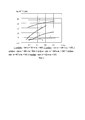
На фиг. 2 представлены экспериментальные зависимости ТКС (αR) многослойного тонкопленочного тензорезистора из взаимочередующихся нанослоев металла с положительным ТКС и металлом с отрицательным ТКС и отдельного нанослоя из металла с положительным ТКС в нижнем нанослое гетероструктуры от количества циклов (m2) совместного напыления этих металлов. На фиг. 2 представлены следующие зависимости:FIG. 2 shows the experimental dependences of the TCR (α R ) of a multilayer thin-film strain gauge made of alternating nanolayers of metal with a positive TCR and a metal with a negative TCR and a separate nanolayer of metal with a positive TCR in the lower nanolayer of the heterostructure on the number of cycles (m 2 ) of joint deposition of these metals. FIG. 2 shows the following dependencies:
1 график - при а=3,0 и n1=0,5;1 graph - with a = 3.0 and n 1 = 0.5;
2 график - при а=4,0 и n1=0,5;2 graph - with a = 4.0 and n 1 = 0.5;
3 график - при а=4,0 и n1=0,6;3 graph - with a = 4.0 and n 1 = 0.6;
4 график - при а=1,0 и n1=4,0;4 graph - with a = 1.0 and n 1 = 4.0;
5 график - при а=0,7 и n1=5,0;5 graph - with a = 0.7 and n 1 = 5.0;
6 график - при а=0,2 и n1=2,0.6 graph - with a = 0.2 and n 1 = 2.0.
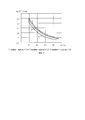
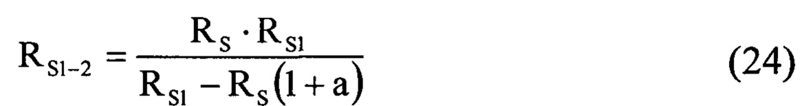
На фиг 3 представлены экспериментальные зависимости ТКС многослойного тонкопленочного тензорезистора из взаимочередующихся нанонослоев металла с положительным ТКС и металла с отрицательным ТКС и отдельного верхнего нанослоя из металла с положительным ТКС и с нижним нанослоем также из металла с положительным ТКС. На фиг. 3 представлены следующие зависимости:Figure 3 shows the experimental dependences of the TCR of a multilayer thin-film strain gauge made of interleaved nanolayers of metal with a positive TCR and a metal with a negative TCR and a separate upper nanolayer of metal with a positive TCR and with a lower nanolayer also made of metal with a positive TCR. FIG. 3 shows the following dependencies:
1 график - при n1=1,0;1 graph - with n 1 = 1.0;
2 график - при n1=1,5;2 graph - with n 1 = 1.5;
3 график - при n1=4,0.3 graph - with n 1 = 4.0.
Рассматриваемую гетероструктуру резистивного слоя тонкопленочного тензорезистора формируют по двум вариантам:The considered heterostructure of the resistive layer of a thin-film strain gauge is formed in two ways:
- с нижним слоем из материала с отрицательным ТКС (первый вариант);- with a lower layer of material with negative TCS (first option);
- с нижним слоем из материала с положительным ТКС (второй вариант).- with a lower layer of material with a positive TCS (second option).
Сопротивление сформированной нижней пленки r1 определяют исходя из выражений:The resistance of the formed lower film r 1 is determined based on the expressions:
- для первого варианта, формула 1:- for the first option, formula 1:
![]()
![]()
- для второго варианта, формула 2:- for the second option, formula 2:
![]()
![]()
где m1, m'1 - количество циклов напыления при формировании нижней пленки для первого и второго варианта соответственно, определяют по формулам:where m 1 , m ' 1 - the number of spraying cycles during the formation of the lower film for the first and second options, respectively, is determined by the formulas:
m1=M⋅t, m'1=M⋅t'1,m 1 = M⋅t, m ' 1 = M⋅t' 1 ,
где М - скорость вращения карусели подложек;where M is the rotation speed of the substrate carousel;
t1, t'1 - время напыления нижнего нанослоя по первому и второму вариантам соответственно;t 1 , t ' 1 - the time of spraying the lower nanolayer according to the first and second options, respectively;
ΔρS1, ΔρS1 - приращения поверхностных сопротивлений монослоев, которые формируются за каждый цикл напыления из металлов с отрицательным и положительным ТКС соответственно;Δρ S1 , Δρ S1 - increments of surface resistances of monolayers, which are formed during each spraying cycle from metals with negative and positive TCS, respectively;
RS1, RS2 - удельное поверхностное сопротивление нанослоя из первого и второго металла соответственно;R S1 , R S2 - specific surface resistance of the nanolayer of the first and second metal, respectively;
N - число квадратов тензорезистора.N is the number of squares of the strain gage.
Сопротивление последующего нанослоя r2 из взаимочередующихся нанослоев двух материалов задают исходя из соотношения:The resistance of the subsequent nanolayer r 2 of alternating nanolayers of two materials is set based on the ratio:
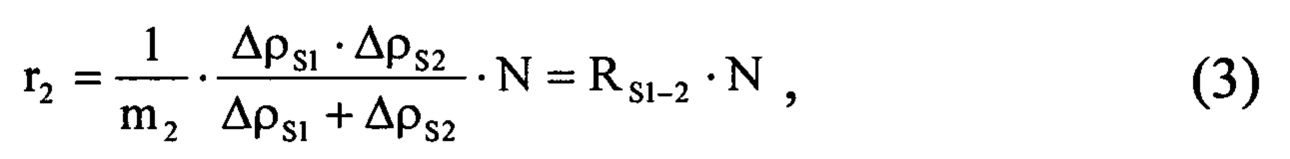
где m2 - количество циклов совместного напыления взаимочередующихся нанослоев материалов с противоположными по знаку ТКС определяют по формуле 4:where m 2 is the number of cycles of joint spraying of alternating nanolayers of materials with TCR opposite in sign is determined by formula 4:
![]()
![]()
где t2 - время совместного напыления нанослоев;where t 2 is the time of joint deposition of nanolayers;
М - скорость вращения карусели подложек.M is the rotation speed of the substrate carousel.
Сопротивление последнего верхнего нанослоя r3 из материала с положительным ТКС определяют по формуле:The resistance of the last upper nanolayer r 3 from a material with a positive TCR is determined by the formula:
![]()
![]()
где m3 - количество циклов напыления только нанослоя из резистивного материала с положительным ТКС определяют по формуле:where m 3 is the number of cycles of spraying only a nanolayer of a resistive material with a positive TCS is determined by the formula:
![]()
![]()
где t3 - время напыления при формировании последнего (верхнего) нанослоя;where t 3 is the spraying time during the formation of the last (upper) nanolayer;
М - скорость вращения карусели подложек.M is the rotation speed of the substrate carousel.
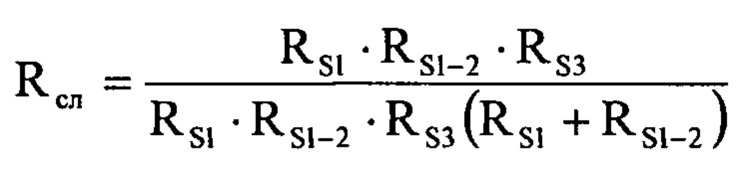
Тогда общее сопротивление резистивного слоя Rоб рассчитывают с помощью эквивалентной схемы из трех параллельно соединенных резисторов по формуле:Then the total resistance of the resistive layer R about is calculated using an equivalent circuit of three parallel-connected resistors according to the formula:
![]()
![]()
Общее сопротивление тонкопленочного тензорезистора с исследуемой структурой резистивного слоя определяют выражениями:The total resistance of a thin-film strain gauge with the investigated structure of the resistive layer is determined by the expressions:
для первого варианта по формуле:for the first option according to the formula:
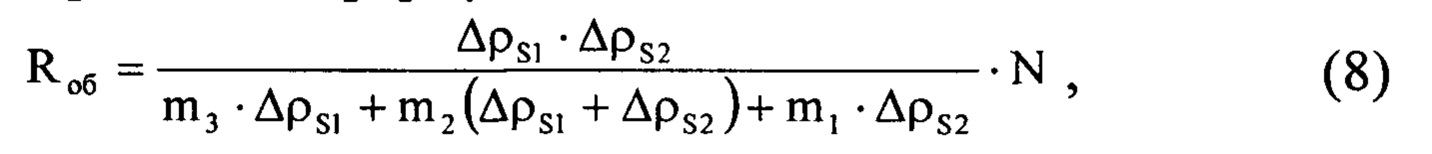
где эквивалентное удельное поверхностное сопротивление слоя определяют выражениемwhere the equivalent specific surface resistance of the layer is determined by the expression
m1 - количество циклов напыления при формировании нижней пленки для первого и второго варианта соответственно;m 1 - the number of spraying cycles during the formation of the lower film for the first and second options, respectively;
m2 - количество циклов совместного напыления взаимочередующихся нанослоев материалов с противоположными по знаку ТКС, определяют по формуле 4;m 2 - the number of cycles of joint spraying of alternating nanolayers of materials with opposite signs of the TCS, is determined by the formula 4;
m3 - количество циклов напыления только нанослоя из резистивного материала с положительным ТКС, определяется по формуле 6;m 3 - the number of cycles of spraying only a nanolayer of a resistive material with a positive TCR, is determined by the formula 6;
- для второго варианта - по формуле:- for the second option - according to the formula:
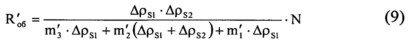
где эквивалентное удельное поверхностное сопротивление слоя определяют выражением:where the equivalent surface resistivity of the layer is determined by the expression:

m'1 - количество циклов напыления при формировании нижней пленки;m ' 1 - the number of spraying cycles during the formation of the lower film;
m'2, m'3 - количество циклов совместного напыления взаимочередующихся нанослоев и напыления только слоя из материала с положительным ТКС соответственно для второго варианта.m ' 2 , m' 3 - the number of cycles of joint spraying of alternating nanolayers and spraying of only a layer of material with a positive TCR, respectively, for the second option.
Зависимость сопротивления многослойного тонкопленочного тензорезистора с рассматриваемой структурой резистивного слоя от температуры Т определяют следующими выражениями:The dependence of the resistance of a multilayer thin-film strain gauge with the considered structure of the resistive layer on the temperature T is determined by the following expressions:
- для первого варианта (принимается, что m3=am1; n1=Δρs2/Δρs1) формула 10:- for the first option (it is assumed that m 3 = am 1 ; n 1 = Δρ s2 / Δρ s1 ) formula 10:

- для второго варианта (принимается, что m'3=а1m'1) формула 11:- for the second option (it is assumed that m ' 3 = a 1 m' 1 ) formula 11:
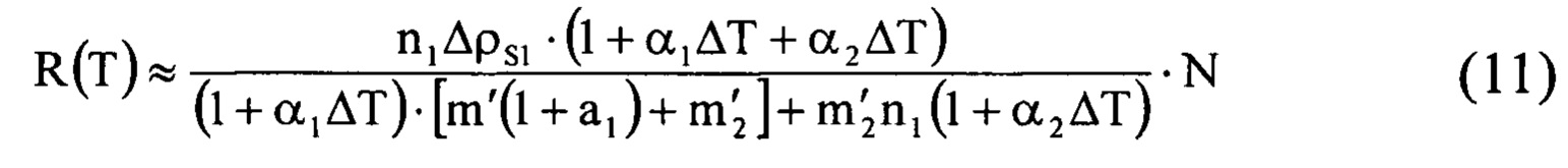
Учитывая, что формулы (10) и (11), в свою очередь, тождественны известному выражению R (Т) ≈ RO (1+αR ΔT), ТКС (αR) для многослойного тонкопленочного тензорезистора со структурой резистивного слоя из взаимочередующихся нанослоев и отдельным слоем из материала с положительным ТКС его определяют выражениями:Taking into account that formulas (10) and (11), in turn, are identical to the well-known expression R (T) ≈ R O (1 + α R ΔT), TCR (α R ) for a multilayer thin-film strain gauge with a resistive layer structure of alternating nanolayers and a separate layer of material with a positive TCS, it is determined by the expressions:
- для первого варианта формула 12:- for the first option, formula 12:

или через параметр - время напыления t1 и t2:or through the parameter - the spraying time t 1 and t 2 :

где mоб - общее количество циклов напыления, необходимое для обеспечения требуемой величины удельного поверхностного сопротивления резистивного слоя RS,where m about - the total number of spraying cycles required to ensure the required value of the specific surface resistance of the resistive layer R S ,
![]()
![]()
- коэффициент а характеризует соотношение циклов напыления m3 и m1 отдельных нанослоев только из материала с отрицательным ТКС.- coefficient a characterizes the ratio of the spraying cycles m 3 and m 1 of individual nanolayers only from a material with a negative TCR.
Из анализа формул (12) и (13) следует, что условие возможности управления величиной ТКС многослойной резистивной гетероструктуры определяют следующим неравенством |а α2|<|n1 α1|.From the analysis of formulas (12) and (13) it follows that the condition for the possibility of controlling the TCR value of a multilayer resistive heterostructure is determined by the following inequality | а α 2 | <| n 1 α 1 |.
- для второго варианта формула 15:- for the second option, formula 15:
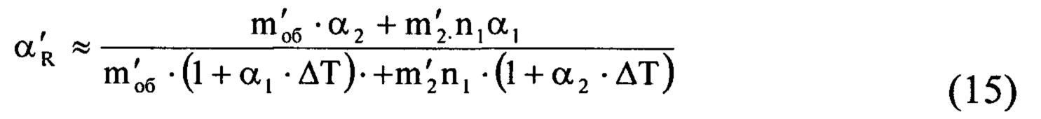
или та же самая формула, но выраженная через параметр время напыления t1 и t2 формула 16:or the same formula, but expressed in terms of the spraying time parameter t 1 and t 2 formula 16:

где m'об - общее количество циклов напыления, необходимое для обеспечения требуемой величины удельного поверхностного сопротивления резистивного слоя RS,where m ' about - the total number of spraying cycles required to ensure the required value of the specific surface resistance of the resistive layer R S ,
![]()
![]()
- коэффициент a1 характеризует соотношение циклов напыления m3 и m1 отдельных нанослоев только из материала с положительным ТКС.- the coefficient a 1 characterizes the ratio of the spraying cycles m 3 and m 1 of individual nanolayers only from a material with a positive TCR.
Из анализа полученных формул (12) и (15) следует, что условием обеспечения ТКС многослойного тонкопленочного тензорезистора, близкого к нулевому значению, с рассмотренными вариантами гетероструктуры резистивного слоя является:From the analysis of the obtained formulas (12) and (15), it follows that the condition for ensuring the TCR of a multilayer thin-film strain gauge close to zero with the considered variants of the heterostructure of the resistive layer is:
- для первого варианта формула 18:- for the first option, formula 18:
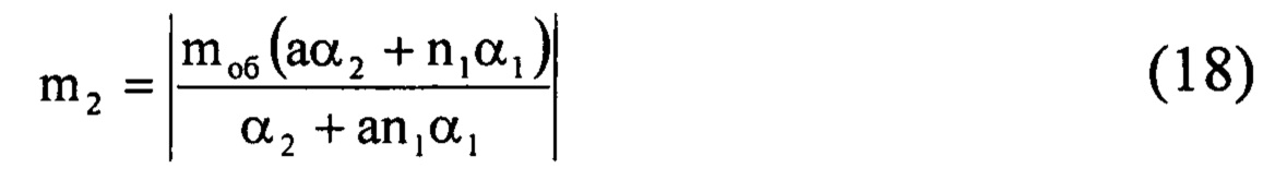
или выраженное через время напыления t2 по формуле 19:or expressed through the spraying time t 2 according to the formula 19:
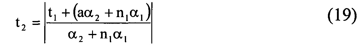
- для второго варианта формула 20:- for the second option, formula 20:
или выраженное через время напыления t'2 по формуле 21:or expressed through the spraying time t ' 2 according to the formula 21:
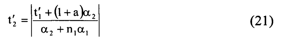
На фиг. 2 представлены экспериментальные зависимости ТКС (αR) многослойного тонкопленочного тензорезистора из взаимочередующихся нанослоев металла с положительным ТКС и металлом с отрицательным ТКС и отдельного нанослоя из металла с положительным ТКС в нижнем нанослое гетероструктуры от количества циклов (m2) совместного напыления этих металлов.FIG. 2 shows the experimental dependences of the TCR (α R ) of a multilayer thin-film strain gauge made of alternating nanolayers of metal with a positive TCR and a metal with a negative TCR and a separate nanolayer of metal with a positive TCR in the lower nanolayer of the heterostructure on the number of cycles (m 2 ) of joint deposition of these metals.
Как видно из представленных зависимостей, для варианта с нижним нанослоем из металла с отрицательным ТКС обеспечить общую величину ТКС многослойного тонкопленочного тензорезистора, близкую к нулевому значению, возможно или при величине следующих коэффициентов а=1,0 и n1=4,0 (см. фиг 2, зависимость 4), или при значении коэффициентов а ≈ 0,2 и n1=2,0 (см. фиг 2, зависимость 6).As can be seen from the presented dependences, for the variant with a lower nanolayer made of metal with a negative TCR, it is possible to provide the total TCR value of a multilayer thin-film strain gage close to zero, either with the following coefficients a = 1.0 and n 1 = 4.0 (see. Fig. 2, dependence 4), or with the value of the coefficients a ≈ 0.2 and n 1 = 2.0 (see Fig. 2, dependence 6).
То есть, количество циклов напыления при формировании верхнего нанослоя резистивной гетероструктуры из металла с положительным ТКС - должно быть не больше 0,2 количества циклов напыления нижнего нанослоя при скорости напыления нанослоев из металла с положительным ТКС, превышающей скорость напыления нанослоев из металла с отрицательным ТКС примерно в 2,0 раза). При одинаковой же скорости напыления двух металлов, когда n1=1,0, величина коэффициента а не должна превышать 0,1 т.е. количество циклов напыления при формировании верхнего нанослоя из металла с положительным ТКС должно быть не больше 0,1 числа циклов напыления нижнего нанослоя структуры из металла с отрицательным ТКС).That is, the number of deposition cycles during the formation of the upper nanolayer of a resistive heterostructure from a metal with a positive TCR should be no more than 0.2 of the number of deposition cycles of the lower nanolayer at a deposition rate of nanolayers of metal with a positive TCR, which exceeds the rate of deposition of nanolayers from a metal with a negative TCR approximately 2.0 times). At the same rate of deposition of two metals, when n 1 = 1.0, the value of the coefficient a should not exceed 0.1, i.e. the number of spraying cycles during the formation of the upper nanolayer from a metal with a positive TCR should be no more than 0.1 of the number of spraying cycles of the lower nanolayer of a metal structure with a negative TCR).
На фиг. 3 представлены экспериментальные зависимости ТКС многослойного тонкопленочного тензорезистора из взаимочередующихся нанонослоев металла с положительным ТКС и металла с отрицательным ТКС и отдельного верхнего нанослоя из металла с положительным ТКС и с нижним нанослоем также из металла с положительным ТКС.FIG. 3 shows the experimental dependences of the TCR of a multilayer thin-film strain gauge made of alternating nanolayers of metal with a positive TCR and a metal with a negative TCR and a separate upper nanolayer of metal with a positive TCR and with a lower nanolayer also made of metal with a positive TCR.
Для варианта с нижним нанослоем гетероструктуры из металла с положительным ТКС обеспечить величину ТКС многослойного тонкопленочного тензорезистора, близкую к нулевому значению, возможно при значениях коэффициента n1>1,5 (см. фиг 3). Причем с увеличением коэффициента n1 (например при n1=4,0, график 3 на фиг. 3) ТКС многослойного тонкопленочного тензорезистора приближается к нулевому значению при меньшем значении числа циклов совместного напыления монослоев двух резистивных материалов.For a variant with a lower nanolayer of a heterostructure made of a metal with a positive TCR, to provide a TCR value of a multilayer thin-film strain gauge close to zero, it is possible with values of the coefficient n 1 > 1.5 (see Fig. 3). Moreover, with an increase in the coefficient n 1 (for example, when n 1 = 4.0,
Таким образом, для рассмотренных вариантов формирования резистивного слоя со структурой из взаимочередующихся нанослоев двух металлов с противоположными по знаку ТКС и отдельным нанослоем (верхним) из материала с положительным ТКС для обеспечения ТКС многослойного тонкопленочного тензорезистора, близкого к нулевому значению, требуется обеспечить превышение скорости напыления монослоев из металла с положительным ТКС над скоростью напыления монослоев из металла с отрицательным ТКС примерно в 2,0 раза при нижнем нанослое структуры из металла с отрицательным ТКС и более, чем в 4,5 раза, при нижнем нанослое структуры из металла с положительным ТКС. Такое условие, в свою очередь, усложняет технологию формирования резистивного слоя с нижним нанослоем из металла с положительным ТКС.Thus, for the considered options for the formation of a resistive layer with a structure of alternating nanolayers of two metals with opposite TCR signs and a separate nanolayer (upper) made of a material with a positive TCR, to ensure TCR of a multilayer thin-film strain gauge close to zero, it is required to ensure that the deposition rate of monolayers is exceeded. from a metal with a positive TCR over the deposition rate of monolayers from a metal with a negative TCR by about 2.0 times for the lower nanolayer of a metal structure with a negative TCR and more than 4.5 times, with a lower nanolayer of a metal structure with a positive TCR. This condition, in turn, complicates the technology of forming a resistive layer with a lower nanolayer of a metal with a positive TCS.
Из результатов экспериментальных исследований характеристик многослойной резистивной гетероструктуры из взаимочередующихся нанослоев двух металлов и отдельного верхнего нанослоя из металла с положительным ТКС определен следующий технологический маршрут формирования:Based on the results of experimental studies of the characteristics of a multilayer resistive heterostructure of alternating nanolayers of two metals and a separate upper nanolayer of a metal with a positive TCS, the following technological route of formation was determined:
- методом магнетронного напыления при вращающейся карусели при количестве циклов напыления m1 формируют нижний нанослой резистивной структуры из металла с отрицательным ТКС до достижения величины удельного поверхностного сопротивления определяемой формулой:- by the method of magnetron sputtering with a rotating carousel with the number of spraying cycles m 1 , a lower nanolayer of a resistive structure is formed from a metal with a negative TCR until the specific surface resistance is determined by the formula:
![]()
![]()
Расчетную величину удельного поверхностного сопротивления этого нанослоя определяют по формуле:The calculated value of the specific surface resistance of this nanolayer is determined by the formula:
![]()
![]()
где RS - требуемая величина поверхностного сопротивления многослойной резистивной гетероструктуры (определяется конструктивными особенностями формируемой тензосхемы).where R S is the required value of the surface resistance of the multilayer resistive heterostructure (determined by the design features of the formed strain gauge).
Многослойную гетероструктуру, получают методом магнетронного напыления при вращающейся карусели одновременно с двух мишеней последовательно, при этом формируют слой резистивной гетероструктуры из взаимочередующихся нанослоев двух металлов при количестве циклов совместного напыления m2, которые рассчитывают по формуле (18).A multilayer heterostructure is obtained by magnetron sputtering with a rotating carousel simultaneously from two targets in succession, while a layer of resistive heterostructure is formed from alternating nanolayers of two metals with the number of co-deposition cycles m 2 , which are calculated by formula (18).
При этом расчетную величину поверхностного сопротивления RS1-2 резистивного слоя из взаимочередующихся нанослоев определяют формулой:In this case, the calculated value of the surface resistance R S1-2 of a resistive layer of alternating nanolayers is determined by the formula:
Скорость напыления нанослоев из металла с положительным ТКС выбирается примерно в 2,0 раза больше скорости напыления нанослоев из металла с отрицательным ТКС (т.е. n1 ~ 2,0).The rate of deposition of nanolayers from a metal with a positive TCS is chosen to be approximately 2.0 times higher than the rate of spraying of nanolayers from a metal with a negative TCS (ie, n 1 ~ 2.0).
Многослойную гетероструктуру получают методом магнетронного напыления при вращающейся карусели в течение m3 - циклов напыления (m3 = am1), при этом формируют слой резистивной гетероструктуры из металла с положительным ТКС до достижения величины удельного поверхностного сопротивления этого нанослоя RS3=RS1×1/а, а значение коэффициента а выбирают из условия а ~ 0,2. При этом скорость напыления нанослоев из металла с положительным ТКС обеспечивают не менее, чем в 2,0 раза выше скорости напыления нанослоев из металла с отрицательным ТКС. Требуемую величину удельного поверхностного сопротивления RS3 последнего (верхнего) нанослоя структуры рассчитывают по формуле:A multilayer heterostructure is obtained by magnetron sputtering with a rotating carousel for m 3 - deposition cycles (m 3 = am 1 ), while a layer of resistive heterostructure is formed from a metal with a positive TCR until the specific surface resistance of this nanolayer is reached R S3 = R S1 × 1 / a, and the value of the coefficient a is chosen from the condition a ~ 0.2. In this case, the rate of deposition of nanolayers from metal with a positive TCR is provided not less than 2.0 times higher than the rate of spraying of nanolayers from metal with a negative TCR. The required specific surface resistance R S3 of the last (upper) nanolayer of the structure is calculated by the formula:
Контроль окончания процесса напыления тонкой пленки осуществляют по сопротивлению свидетеля на карусели подложек. Величину сопротивления свидетеля задают заранее, исходя из количества квадратов напыляемой пленки на свидетель и требуемой величины удельного поверхностного сопротивления создаваемой многослойной гетероструктуры. Процесс контроля осаждения многослойной гетероструктуры с помощью свидетеля на карусели подложек позволяет управлять величиной удельного поверхностного сопротивления создаваемой многослойной гетероструктуры и величиной ее ТКС.Control of the end of the thin film deposition process is carried out by the resistance of the witness on the carousel of substrates. The value of the resistance of the witness is set in advance, based on the number of squares of the sprayed film on the witness and the required value of the specific surface resistance of the created multilayer heterostructure. The process of monitoring the deposition of a multilayer heterostructure with the help of a witness on a carousel of substrates makes it possible to control the value of the specific surface resistance of the created multilayer heterostructure and the value of its TCR.
Технический результат заключается в повышении температурной стабильности начального выходного сигнала тензосхемы датчика в широком температурном диапазоне от криогенных температур до температуры +250°С, обеспеченной технологией формообразования многослойной тонкопленочной гетероструктуры для получения тензосхемы на чувствительных элементах датчиков избыточного и абсолютного давления с заданной величиной удельного поверхностного сопротивления и минимальным положительным ТКС тензорезисторов.The technical result consists in increasing the temperature stability of the initial output signal of the sensor strain gauge in a wide temperature range from cryogenic temperatures to + 250 ° C, provided by the technology of forming a multilayer thin-film heterostructure to obtain a strain gauge on the sensitive elements of gauge and absolute pressure sensors with a given value of specific surface resistance and minimum positive TCR of strain gages.
Claims (32)
Priority Applications (1)
| Application Number | Priority Date | Filing Date | Title |
|---|---|---|---|
| RU2020140228A RU2750503C1 (en) | 2020-12-07 | 2020-12-07 | Method for producing a multilayer thin-film heterostructure with a given value of specific surface resistance |
Applications Claiming Priority (1)
| Application Number | Priority Date | Filing Date | Title |
|---|---|---|---|
| RU2020140228A RU2750503C1 (en) | 2020-12-07 | 2020-12-07 | Method for producing a multilayer thin-film heterostructure with a given value of specific surface resistance |
Publications (1)
| Publication Number | Publication Date |
|---|---|
| RU2750503C1 true RU2750503C1 (en) | 2021-06-29 |
Family
ID=76820154
Family Applications (1)
| Application Number | Title | Priority Date | Filing Date |
|---|---|---|---|
| RU2020140228A RU2750503C1 (en) | 2020-12-07 | 2020-12-07 | Method for producing a multilayer thin-film heterostructure with a given value of specific surface resistance |
Country Status (1)
| Country | Link |
|---|---|
| RU (1) | RU2750503C1 (en) |
Cited By (1)
| Publication number | Priority date | Publication date | Assignee | Title |
|---|---|---|---|---|
| RU2782306C1 (en) * | 2021-07-29 | 2022-10-25 | Закрытое акционерное общество Научно-инженерный центр "ИНКОМСИСТЕМ" | Method for creating a nanolayer of amorphous silicon of a predetermined thickness when waterproofing a substrate |
Citations (9)
| Publication number | Priority date | Publication date | Assignee | Title |
|---|---|---|---|---|
| EP0348658A2 (en) * | 1988-05-28 | 1990-01-03 | Robert Bosch Gmbh | Thick film force or pressure transducer |
| RU2089656C1 (en) * | 1993-12-23 | 1997-09-10 | Ольга Викторовна Гончарова | Method of production of photosensitive resistive and optically nonlinear thin-filmed heterostructures based on semiconductor and dielectric materials |
| US20050068989A1 (en) * | 2003-09-30 | 2005-03-31 | Herbert Patrick C. | Microelectromechanical strain gauge |
| RU2280905C2 (en) * | 2001-02-05 | 2006-07-27 | Иркутский государственный лингвистический университет | Material for metal-film resistive layer and method for producing a resistive layer on basis of said material |
| RU2326460C1 (en) * | 2007-01-23 | 2008-06-10 | ФГУП "НИИ физических измерений" | Method of manufacture of high-temperature thin-film resistor |
| RU2396634C2 (en) * | 2008-10-09 | 2010-08-10 | Учреждение Российской академии наук Институт проблем технологии микроэлектроники и особочистых материалов РАН (ИПТМ РАН) | METHOD OF MAKING HETEROGENEOUS p-n JUNCTION BASED ON ZINC OXIDE NANORODS |
| RU2398195C1 (en) * | 2009-08-26 | 2010-08-27 | Евгений Михайлович Белозубов | Method of making nano- and micro-electromechanical pressure sensor system and pressure sensor based on said system |
| RU2411474C1 (en) * | 2010-02-15 | 2011-02-10 | Евгений Михайлович Белозубов | High precision pressure sensor based on nano- and micro-electromechanical system with thin-film tensoresistors |
| RU2498249C1 (en) * | 2012-05-23 | 2013-11-10 | Открытое акционерное общество "Научно-исследовательский институт физических измерений" | Manufacturing method of resistive strain-gauge pressure sensor based on thin-film nano- and microelectromechanical system |
-
2020
- 2020-12-07 RU RU2020140228A patent/RU2750503C1/en active
Patent Citations (9)
| Publication number | Priority date | Publication date | Assignee | Title |
|---|---|---|---|---|
| EP0348658A2 (en) * | 1988-05-28 | 1990-01-03 | Robert Bosch Gmbh | Thick film force or pressure transducer |
| RU2089656C1 (en) * | 1993-12-23 | 1997-09-10 | Ольга Викторовна Гончарова | Method of production of photosensitive resistive and optically nonlinear thin-filmed heterostructures based on semiconductor and dielectric materials |
| RU2280905C2 (en) * | 2001-02-05 | 2006-07-27 | Иркутский государственный лингвистический университет | Material for metal-film resistive layer and method for producing a resistive layer on basis of said material |
| US20050068989A1 (en) * | 2003-09-30 | 2005-03-31 | Herbert Patrick C. | Microelectromechanical strain gauge |
| RU2326460C1 (en) * | 2007-01-23 | 2008-06-10 | ФГУП "НИИ физических измерений" | Method of manufacture of high-temperature thin-film resistor |
| RU2396634C2 (en) * | 2008-10-09 | 2010-08-10 | Учреждение Российской академии наук Институт проблем технологии микроэлектроники и особочистых материалов РАН (ИПТМ РАН) | METHOD OF MAKING HETEROGENEOUS p-n JUNCTION BASED ON ZINC OXIDE NANORODS |
| RU2398195C1 (en) * | 2009-08-26 | 2010-08-27 | Евгений Михайлович Белозубов | Method of making nano- and micro-electromechanical pressure sensor system and pressure sensor based on said system |
| RU2411474C1 (en) * | 2010-02-15 | 2011-02-10 | Евгений Михайлович Белозубов | High precision pressure sensor based on nano- and micro-electromechanical system with thin-film tensoresistors |
| RU2498249C1 (en) * | 2012-05-23 | 2013-11-10 | Открытое акционерное общество "Научно-исследовательский институт физических измерений" | Manufacturing method of resistive strain-gauge pressure sensor based on thin-film nano- and microelectromechanical system |
Cited By (2)
| Publication number | Priority date | Publication date | Assignee | Title |
|---|---|---|---|---|
| RU2782306C1 (en) * | 2021-07-29 | 2022-10-25 | Закрытое акционерное общество Научно-инженерный центр "ИНКОМСИСТЕМ" | Method for creating a nanolayer of amorphous silicon of a predetermined thickness when waterproofing a substrate |
| RU2818204C1 (en) * | 2022-12-27 | 2024-04-25 | Акционерное общество "Научно-исследовательский институт электронно-механических приборов" | Method of making thin-film precision resistor |
Similar Documents
| Publication | Publication Date | Title |
|---|---|---|
| JP7832402B2 (en) | Strain gauge | |
| Kazi et al. | The electromechanical behavior of nichrome (80/20 wt.%) film | |
| Han et al. | MEMS-based Pt film temperature sensor on an alumina substrate | |
| US7963171B2 (en) | High temperature strain gages | |
| US6729187B1 (en) | Self-compensated ceramic strain gage for use at high temperatures | |
| CN107267944B (en) | High-temperature film half-bridge resistance strain gauge with temperature self-compensation function and preparation method thereof | |
| EP0035351A2 (en) | Deformable flexure element for strain gage transducer and method of manufacture | |
| CN111174687B (en) | Flexible strain sensor chip with temperature compensation element and preparation method thereof | |
| Zhang et al. | A bilayer thin-film strain gauge with temperature self-compensation | |
| RU2750503C1 (en) | Method for producing a multilayer thin-film heterostructure with a given value of specific surface resistance | |
| Kalpana et al. | Development of the invar36 thin film strain gauge sensor for strain measurement | |
| RU2326460C1 (en) | Method of manufacture of high-temperature thin-film resistor | |
| EP4350313A1 (en) | Strain resistance film, physical quantity sensor, and method for manufacturing the strain resistance film | |
| JP2001221696A (en) | Temperature-sensitive and strain-sensitive composite sensor | |
| Wang et al. | Effect of annealing on the performance of nickel thermistor on polyimide substrate | |
| JP2024532966A (en) | Thin-film sensor with improved sensitivity | |
| JP2585681B2 (en) | Metal thin film resistive strain gauge | |
| Gregory et al. | A low TCR nanocomposite strain gage for high temperature aerospace applications | |
| JP7743266B2 (en) | Strain gauge and its manufacturing method | |
| Zarfl et al. | Electro-mechanical properties and oxidation behaviour of TiAlNxOy thin films at high temperatures | |
| AU4496200A (en) | Self-compensated ceramic strain gage for use at high temperatures | |
| Löffler et al. | Manganin thin film sensor for force sensing | |
| Mikhailov et al. | Control and optimization of technological processes for forming nanoscale films for sensitive sensor elements | |
| JP6850642B2 (en) | Pressure sensor | |
| RU2544864C1 (en) | Method of manufacturing of thin film nano- and microelectromechanical system of mechanical values transmitter |