RU2024922C1 - Control command input device - Google Patents
Control command input device Download PDFInfo
- Publication number
- RU2024922C1 RU2024922C1 SU5006085A RU2024922C1 RU 2024922 C1 RU2024922 C1 RU 2024922C1 SU 5006085 A SU5006085 A SU 5006085A RU 2024922 C1 RU2024922 C1 RU 2024922C1
- Authority
- RU
- Russia
- Prior art keywords
- input
- output
- inputs
- outputs
- counter
- Prior art date
Links
- 238000009434 installation Methods 0.000 claims 3
- 239000000126 substance Substances 0.000 abstract 1
- 230000004044 response Effects 0.000 description 3
- 238000010586 diagram Methods 0.000 description 1
- 230000010365 information processing Effects 0.000 description 1
- 238000012795 verification Methods 0.000 description 1
Images
Landscapes
- Communication Control (AREA)
Abstract
Description
Изобретение относится к вычислительной технике и технике связи, а именно к системам управления техническими средствами связи и предназначено для ввода управляющей информации. The invention relates to computing and communications, and in particular to control systems for technical communications and is intended to enter control information.
Целью изобретения является повышение достоверности ввода информации. The aim of the invention is to increase the reliability of the input information.
Устройство позволяет, во-первых, определять длину (количество знаков (символов) в команде) сообщения - команды и, если она не соответствует заданной, то формируется сигнал ошибки, во-вторых, сверять конец команды на соответствие определенному знаку (символу), в-третьих, осуществлять проверку каждого символа в команде, при которой выявляется его соответствие заданному и, в случае несовпадения с заданным, формируется ошибка, а также обеспечивается распределение кодов команд по их классам (типам) в зависимости от их принадлежности к какой-либо подсистеме, например, обслуживания, обработки сообщений, статистики и т.д. The device allows, firstly, to determine the length (number of characters (characters) in the command) of the message - the command and, if it does not match the specified one, an error signal is generated, and secondly, to verify the end of the command for compliance with a certain character (symbol), in thirdly, to check each character in a command, in which its correspondence to the given is revealed and, in case of mismatch with the given, an error is generated, and the codes of the teams are distributed among their classes (types) depending on their belonging to any odsisteme, for example, service, message processing, statistics, etc.
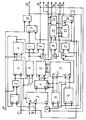
На чертеже представлена функциональная схема устройства для ввода команд управления. The drawing shows a functional diagram of a device for entering control commands.
Устройство содержит первый триггер 1, третий элемент И 2, первый счетчик 3, первый дешифратор 4, блок регистров 5, второй дешифратор 6, четвертый и первый элементы И 7,8, второй триггер 9, пятый элемент И 10, блок мультиплексоров 11, блок сравнения 12, первый элемент НЕ 13, первый элемент ИЛИ 14, третий и второй счетчики 15, 16, блок памяти 17 (постоянное запоминающее устройство), второй и шестой элементы И 18, 19, второй элемент НЕ 20, второй элемент ИЛИ 21, четвертый счетчик 22, третий и четвертый дешифраторы 23, 24 и третий триггер 25 (на чертеже обозначены). Входы и выходы устройства 26-34. The device contains a
Блок регистров 5 содержит N, например 8 или 16 и т.д., восьмиразрядных регистров памяти, выполненных на регистрах 155 ТМ8, 155 ТМ2, у которых информационные (Do-D7) входы поразрядно объединены, а выходы регистров являются (по отдельности) выходами блока 5, входы синхронизации (С) регистров памяти подключены к выходам отдельного N-разрядного кольцевого регистра сдвига, выполненного, например, на последовательно включенных регистрах 155 ИР1, на вход(ы) синхронизации которого подается сигнал тактовой частоты (с выхода элемента И2), а в один из разрядов регистра сдвига, например, по сигналу сброса записывается логическая единица, которая движется по регистру под действием тактовых импульсов, входы сброса регистров памяти объединены и подключены через элементы НЕ (для согласования) к входу сброса блока 5.The
К выходам дешифратора 6 подключены элементы НЕ, выходы которых объединены по схеме И и образуют полный 2 n дешифратор.The NOT elements are connected to the outputs of the decoder 6, the outputs of which are combined according to the AND circuit and form a complete 2 n decoder.
Устройство работает следующим образом. The device operates as follows.
После включения напряжения питания и подачи сигнала "Сброс" на вход 27 устройства его блоки с памятью (регистры, счетчики, триггеры) устанавливаются в исходное состояние. After turning on the supply voltage and applying the signal "Reset" to the
На входы 26 устройства, а значит, и на информационные входы блока 5 поступает входная информация в параллельном коде посимвольно. Эта входная информация (команды управления или ответы на них) записывается в блок 5 с помощью импульсов тактовой частоты, подаваемой на вход 28 устройства. The inputs of the
Триггер 1 разрешает прохождение импульсов частоты через элемент И 2 на счетчик 3. Последний отсчитывает количество поступающих символов и, если оно не меньше заданного значения, то дешифратор 4 (длины кода команды) сформирует на своем выходе сигнал, который поступит на одни входы элементов И 7, 8. На другие входы этих элементов подается стробирующий сигнал (прямой и инверсный соответственно) с выхода дешифратора 6. Этот дешифратор 6 выделяет разделительный символ, например, "Пробел", означающий конец кода команды.
Таким образом, если длина кода или число его знаков (символов), содержащихся в команде, соответствует заданному значению, то с выхода элемента И 7 будет сформирован сигнал на триггер 9, который перейдет в состояние логической единицы и разрешит прохождение импульсов тактовой частоты через элемент И 10. Это означает, что сигнал (код) команды был в данном случае полным. Thus, if the length of the code or the number of its signs (symbols) contained in the command corresponds to the specified value, then a signal will be generated from the output of the And 7 element to trigger 9, which will go into the state of the logical unit and allow the passage of clock pulses through the And
Если же число символов в команде не соответствует заданному, то с выхода элемента И 7 сигнала не будет, а он появится на выходе элемента И 8. Это означает, что сигнал (код) команды был неполным. Триггер 9 останется в исходном (нулевом) состоянии и не разрешит прохождение импульсов через элемент И 10. С выхода элемента И 8 на выход 2 устройства, в этом случае будет выдан сигнал "Ошибка полноты", а устройство запретит дальнейшую обработку принимаемой информации. При этом сигнал с выхода элемента И 8 поступит через элемент ИЛИ 14 на вход сброса блока 5, который обнулится. If the number of characters in the command does not match the specified one, then there will be no signal from the output of the And 7 element, and it will appear at the output of the And 8. This means that the signal (code) of the command was incomplete.
В случае успешной проверки кода команды на полноту, производится проверка содержимого кода команды на корректность. If the command code is checked for completeness, the contents of the command code are checked for correctness.
В этом случае триггер 9 разрешает прохождение импульсов частоты через элемент И 10 на входы счетчиков 16 и 22. In this case,
Счетчик 16 формирует по очередности адресные коды на входы блока памяти (ПЗУ) 17. The
С выходов ПЗУ 17 считываются хранящиеся в нем коды символов, соответствующие первому знакоместу для всех допустимых команд управления (или ответов на них), на одни из входов блока 12. На других входах блока 12 присутствует в это время код первого по знакоместу символа, принятого и записанного в блоке 5. Поскольку триггер 1 по сигналу, полученному с выхода дешифратора 4, переключился в состояние логической единицы, то под действием сигнала логического нуля, подаваемого с инверсного выхода триггера 1 на вход элемента И 2, будет запрещено прохождение импульсов частоты на вход синхронизации блока 5. From the outputs of the
Информация о команде управления хранится в блоке 5 и считывается из него посимвольно с помощью счетчика 15 и блока мультиплексоров 11. Счетчик 15 формирует новый адрес на блоки 11 и 17 после того, как счетчик 16 "прокрутит" (переберет) адреса всех символов первого знакоместа в команде. В результате с выходов блока 11 на входы блоков 12 и 22 и на выходы 1 устройства выдается новый код символа после того, как будут проверены с помощью счетчика 16 всевозможные значения символов, коды которых хранятся в виде таблицы в ПЗУ 17. Information about the control command is stored in
При этом с выходов дешифратора 24 на выходы 6 устройства формируются сигналы-признаки в соответствии с принятой в системе классификацией (типом) команд, содержащихся, например, в первом знаке команды. At the same time, from the outputs of the
При совпадении кодов символов с выхода блока 12 через элемент И 18, стробируемый импульсами инверсной частоты, на счетчик 22 поступает импульс. Число импульсов сравнения должно соответствовать числу (количеству) символов в коде команды. With the coincidence of the character codes from the output of
Если число таких сравнений будет не менее заданного (оно определяется дешифратором 23), то с выхода блока 23 на триггер 25 сформируется сигнал. Триггер 25 переключится в состояние логической единицы и с его прямого выхода на выход 4 устройства будет выдан сигнал готовности продолжать работу дальше. Это значит, что код принятой команды прошел успешную проверку не только на полноту, но и на корректность, то есть соответствие кодов символов требуемым. If the number of such comparisons is not less than the specified one (it is determined by the decoder 23), then a signal will be generated from the output of
Если же число отсчитанных импульсов сравнения счетчиком 22 окажется меньше заданного, то это означает, что на устройство поступила ложная информация или некорректная команда. При этом с одиночного выхода (последнего разряда) счетчика 15 через элемент И 19, открытый сигналом логической единицы с инверсного плеча триггера 25, выдается на выход 3 устройства сигнал "Ошибка корректности". If the number of counted comparison pulses by the
Этот сигнал поступит через элемент ИЛИ 21 на входы сброса счетчиков 15, 16 и через элемент ИЛИ 14 на вход сброса блока 5. Указанные блоки обнуляются и устройство готово к новому циклу приема команд управления, начинающегося сигналом "Сброс" по входу 1 устройства. This signal will come through the
На этом проверка принятой команды на полноту и корректность завершается. On this, the verification of the received command for completeness and correctness is completed.
В случае правильного ввода кода команды при проверке на его полноту с выхода элемента И 10 на выход 5 устройства будет выдаваться последовательность тактовых импульсов, с помощью которых можно считывать посимвольно код команды или ответного сообщения на выходах 1 устройства. При этом на выходах 6 устройства формируются сигналы - "признаки", означающие принадлежность команды или сообщения определенной подсистеме, например, обслуживания, обработки информации, статистики и т.д., в соответствии с принятой классификацией (типом) команд. If the command code is entered correctly when checking for completeness from the output of the AND 10 element, the
Таким образом, предлагаемое устройство позволит повысить достоверность принимаемой или вводимой из другого устройства информации (в частности команд управления) не только в условиях появления ошибок из-за электромагнитных помех, но также вследствие ошибочных действий человека - оператора, а также расширить функциональные возможности. Thus, the proposed device will improve the reliability of information received or input from another device (in particular, control commands) not only in the event of errors due to electromagnetic interference, but also due to erroneous actions of the human operator, as well as expand the functionality.
Claims (1)
Priority Applications (1)
| Application Number | Priority Date | Filing Date | Title |
|---|---|---|---|
| SU5006085 RU2024922C1 (en) | 1991-08-29 | 1991-08-29 | Control command input device |
Applications Claiming Priority (1)
| Application Number | Priority Date | Filing Date | Title |
|---|---|---|---|
| SU5006085 RU2024922C1 (en) | 1991-08-29 | 1991-08-29 | Control command input device |
Publications (1)
| Publication Number | Publication Date |
|---|---|
| RU2024922C1 true RU2024922C1 (en) | 1994-12-15 |
Family
ID=21587227
Family Applications (1)
| Application Number | Title | Priority Date | Filing Date |
|---|---|---|---|
| SU5006085 RU2024922C1 (en) | 1991-08-29 | 1991-08-29 | Control command input device |
Country Status (1)
| Country | Link |
|---|---|
| RU (1) | RU2024922C1 (en) |
-
1991
- 1991-08-29 RU SU5006085 patent/RU2024922C1/en active
Non-Patent Citations (2)
| Title |
|---|
| Авторское свидетельство СССР N 1334140, кл. G 06F 3/02, 1986. * |
| Авторское свидетельство СССР N 1418640, кл. G 06F 3/02, 1986. * |
Similar Documents
| Publication | Publication Date | Title |
|---|---|---|
| GB2070779A (en) | Apparatus for testing digital electronic circuits | |
| RU2024922C1 (en) | Control command input device | |
| RU1786483C (en) | Input device | |
| SU1365093A1 (en) | Device for simulating communication systems | |
| RU2019034C1 (en) | Error detector | |
| SU978197A1 (en) | Associative on-line memory device | |
| SU1317484A1 (en) | Storage with error correction | |
| SU1124331A2 (en) | System for automatic inspecting of large-scale-integrated circuits | |
| SU1661786A2 (en) | Data transmission system simulator | |
| SU1465892A1 (en) | Device for modeling programming technology | |
| SU1663771A1 (en) | Device for error detection | |
| SU1488828A1 (en) | DEVICE FOR MODELING COMPUTATIONAL SYSTEM | |
| SU1439685A1 (en) | Self-check storage | |
| SU1501023A1 (en) | Data input device | |
| SU1444807A1 (en) | Device for investigating coherence of graphs | |
| SU1425641A1 (en) | Data input device | |
| SU1589256A1 (en) | Device for checking information identity of controlled objects | |
| SU717756A1 (en) | Extremum number determining device | |
| SU1104589A1 (en) | Device for checking writing information in programmable memory units | |
| SU1128267A1 (en) | Device for checking digital units | |
| SU824178A1 (en) | Random event flow generator | |
| RU1772804C (en) | Shift register testing device | |
| SU1640740A1 (en) | Device for monitoring permanent memory units | |
| SU773735A1 (en) | Storage testing device | |
| RU2041487C1 (en) | Device for modeling technology of software development |