KR920010921B1 - Image sensor - Google Patents
Image sensor Download PDFInfo
- Publication number
- KR920010921B1 KR920010921B1 KR1019850001531A KR850001531A KR920010921B1 KR 920010921 B1 KR920010921 B1 KR 920010921B1 KR 1019850001531 A KR1019850001531 A KR 1019850001531A KR 850001531 A KR850001531 A KR 850001531A KR 920010921 B1 KR920010921 B1 KR 920010921B1
- Authority
- KR
- South Korea
- Prior art keywords
- transparent substrate
- light
- information
- thin film
- image sensor
- Prior art date
Links
- 239000000758 substrate Substances 0.000 claims description 37
- 239000010408 film Substances 0.000 claims description 22
- 230000003287 optical effect Effects 0.000 claims description 21
- 239000010409 thin film Substances 0.000 claims description 16
- 238000000034 method Methods 0.000 claims description 9
- 239000000463 material Substances 0.000 claims description 4
- 238000000206 photolithography Methods 0.000 claims description 3
- 230000008569 process Effects 0.000 claims description 3
- 230000004044 response Effects 0.000 claims description 2
- 230000005540 biological transmission Effects 0.000 claims 2
- 230000002093 peripheral effect Effects 0.000 claims 2
- 230000000903 blocking effect Effects 0.000 claims 1
- 229910021645 metal ion Inorganic materials 0.000 claims 1
- 230000035945 sensitivity Effects 0.000 claims 1
- 239000004065 semiconductor Substances 0.000 description 5
- 238000004519 manufacturing process Methods 0.000 description 4
- 238000010586 diagram Methods 0.000 description 3
- 239000011521 glass Substances 0.000 description 3
- 229910004298 SiO 2 Inorganic materials 0.000 description 2
- 229910052776 Thorium Inorganic materials 0.000 description 2
- 150000002500 ions Chemical class 0.000 description 2
- 229910052709 silver Inorganic materials 0.000 description 2
- 229920003002 synthetic resin Polymers 0.000 description 2
- 239000000057 synthetic resin Substances 0.000 description 2
- 230000004075 alteration Effects 0.000 description 1
- 238000003491 array Methods 0.000 description 1
- 230000008901 benefit Effects 0.000 description 1
- 230000015572 biosynthetic process Effects 0.000 description 1
- 238000006243 chemical reaction Methods 0.000 description 1
- 238000009833 condensation Methods 0.000 description 1
- 230000005494 condensation Effects 0.000 description 1
- 239000004020 conductor Substances 0.000 description 1
- 238000000151 deposition Methods 0.000 description 1
- 238000009792 diffusion process Methods 0.000 description 1
- 230000000694 effects Effects 0.000 description 1
- 238000010894 electron beam technology Methods 0.000 description 1
- 238000005530 etching Methods 0.000 description 1
- 230000010354 integration Effects 0.000 description 1
- XEEYBQQBJWHFJM-UHFFFAOYSA-N iron Substances [Fe] XEEYBQQBJWHFJM-UHFFFAOYSA-N 0.000 description 1
- 229910052742 iron Inorganic materials 0.000 description 1
- 239000002184 metal Substances 0.000 description 1
- 229910052751 metal Inorganic materials 0.000 description 1
- 229920002120 photoresistant polymer Polymers 0.000 description 1
- 230000009467 reduction Effects 0.000 description 1
- 229920005989 resin Polymers 0.000 description 1
- 239000011347 resin Substances 0.000 description 1
- 229910001415 sodium ion Inorganic materials 0.000 description 1
Images


Classifications
-
- H—ELECTRICITY
- H01—ELECTRIC ELEMENTS
- H01L—SEMICONDUCTOR DEVICES NOT COVERED BY CLASS H10
- H01L27/00—Devices consisting of a plurality of semiconductor or other solid-state components formed in or on a common substrate
- H01L27/14—Devices consisting of a plurality of semiconductor or other solid-state components formed in or on a common substrate including semiconductor components sensitive to infrared radiation, light, electromagnetic radiation of shorter wavelength or corpuscular radiation and specially adapted either for the conversion of the energy of such radiation into electrical energy or for the control of electrical energy by such radiation
-
- H—ELECTRICITY
- H04—ELECTRIC COMMUNICATION TECHNIQUE
- H04N—PICTORIAL COMMUNICATION, e.g. TELEVISION
- H04N1/00—Scanning, transmission or reproduction of documents or the like, e.g. facsimile transmission; Details thereof
- H04N1/024—Details of scanning heads ; Means for illuminating the original
- H04N1/028—Details of scanning heads ; Means for illuminating the original for picture information pick-up
- H04N1/03—Details of scanning heads ; Means for illuminating the original for picture information pick-up with photodetectors arranged in a substantially linear array
- H04N1/031—Details of scanning heads ; Means for illuminating the original for picture information pick-up with photodetectors arranged in a substantially linear array the photodetectors having a one-to-one and optically positive correspondence with the scanned picture elements, e.g. linear contact sensors
- H04N1/0315—Details of scanning heads ; Means for illuminating the original for picture information pick-up with photodetectors arranged in a substantially linear array the photodetectors having a one-to-one and optically positive correspondence with the scanned picture elements, e.g. linear contact sensors using photodetectors and illumination means mounted on separate supports or substrates or mounted in different planes
- H04N1/0316—Details of scanning heads ; Means for illuminating the original for picture information pick-up with photodetectors arranged in a substantially linear array the photodetectors having a one-to-one and optically positive correspondence with the scanned picture elements, e.g. linear contact sensors using photodetectors and illumination means mounted on separate supports or substrates or mounted in different planes illuminating the scanned image elements through the plane of the photodetector, e.g. back-light illumination
-
- G—PHYSICS
- G02—OPTICS
- G02B—OPTICAL ELEMENTS, SYSTEMS OR APPARATUS
- G02B6/00—Light guides; Structural details of arrangements comprising light guides and other optical elements, e.g. couplings
- G02B6/10—Light guides; Structural details of arrangements comprising light guides and other optical elements, e.g. couplings of the optical waveguide type
- G02B6/12—Light guides; Structural details of arrangements comprising light guides and other optical elements, e.g. couplings of the optical waveguide type of the integrated circuit kind
- G02B6/122—Basic optical elements, e.g. light-guiding paths
- G02B6/124—Geodesic lenses or integrated gratings
- G02B6/1245—Geodesic lenses
-
- H—ELECTRICITY
- H01—ELECTRIC ELEMENTS
- H01L—SEMICONDUCTOR DEVICES NOT COVERED BY CLASS H10
- H01L27/00—Devices consisting of a plurality of semiconductor or other solid-state components formed in or on a common substrate
- H01L27/14—Devices consisting of a plurality of semiconductor or other solid-state components formed in or on a common substrate including semiconductor components sensitive to infrared radiation, light, electromagnetic radiation of shorter wavelength or corpuscular radiation and specially adapted either for the conversion of the energy of such radiation into electrical energy or for the control of electrical energy by such radiation
- H01L27/144—Devices controlled by radiation
- H01L27/146—Imager structures
- H01L27/14601—Structural or functional details thereof
- H01L27/1462—Coatings
- H01L27/14623—Optical shielding
-
- H—ELECTRICITY
- H01—ELECTRIC ELEMENTS
- H01L—SEMICONDUCTOR DEVICES NOT COVERED BY CLASS H10
- H01L27/00—Devices consisting of a plurality of semiconductor or other solid-state components formed in or on a common substrate
- H01L27/14—Devices consisting of a plurality of semiconductor or other solid-state components formed in or on a common substrate including semiconductor components sensitive to infrared radiation, light, electromagnetic radiation of shorter wavelength or corpuscular radiation and specially adapted either for the conversion of the energy of such radiation into electrical energy or for the control of electrical energy by such radiation
- H01L27/144—Devices controlled by radiation
- H01L27/146—Imager structures
- H01L27/14601—Structural or functional details thereof
- H01L27/14625—Optical elements or arrangements associated with the device
-
- H—ELECTRICITY
- H01—ELECTRIC ELEMENTS
- H01L—SEMICONDUCTOR DEVICES NOT COVERED BY CLASS H10
- H01L27/00—Devices consisting of a plurality of semiconductor or other solid-state components formed in or on a common substrate
- H01L27/14—Devices consisting of a plurality of semiconductor or other solid-state components formed in or on a common substrate including semiconductor components sensitive to infrared radiation, light, electromagnetic radiation of shorter wavelength or corpuscular radiation and specially adapted either for the conversion of the energy of such radiation into electrical energy or for the control of electrical energy by such radiation
- H01L27/144—Devices controlled by radiation
- H01L27/146—Imager structures
- H01L27/14643—Photodiode arrays; MOS imagers
-
- H—ELECTRICITY
- H04—ELECTRIC COMMUNICATION TECHNIQUE
- H04N—PICTORIAL COMMUNICATION, e.g. TELEVISION
- H04N1/00—Scanning, transmission or reproduction of documents or the like, e.g. facsimile transmission; Details thereof
- H04N1/024—Details of scanning heads ; Means for illuminating the original
- H04N1/028—Details of scanning heads ; Means for illuminating the original for picture information pick-up
- H04N1/03—Details of scanning heads ; Means for illuminating the original for picture information pick-up with photodetectors arranged in a substantially linear array
- H04N1/031—Details of scanning heads ; Means for illuminating the original for picture information pick-up with photodetectors arranged in a substantially linear array the photodetectors having a one-to-one and optically positive correspondence with the scanned picture elements, e.g. linear contact sensors
- H04N1/0311—Details of scanning heads ; Means for illuminating the original for picture information pick-up with photodetectors arranged in a substantially linear array the photodetectors having a one-to-one and optically positive correspondence with the scanned picture elements, e.g. linear contact sensors using an array of elements to project the scanned image elements onto the photodetectors
-
- H—ELECTRICITY
- H04—ELECTRIC COMMUNICATION TECHNIQUE
- H04N—PICTORIAL COMMUNICATION, e.g. TELEVISION
- H04N23/00—Cameras or camera modules comprising electronic image sensors; Control thereof
- H04N23/50—Constructional details
- H04N23/54—Mounting of pick-up tubes, electronic image sensors, deviation or focusing coils
Abstract
내용 없음.No content.
Description
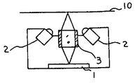
제1도는 종래의 이미지 센서의 일례를 나타낸 단면도.1 is a cross-sectional view showing an example of a conventional image sensor.
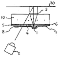
제2도는 종래의 이미지 센서의 다른 예를 나타낸 단면도.2 is a cross-sectional view showing another example of a conventional image sensor.
제3a,b도는 본원 발명에 의한 이미지 센서의 일실시예를 나타낸 구성도로서,3a, b is a configuration diagram showing an embodiment of an image sensor according to the present invention,
제3a도는 단면도.3a is a sectional view.
제3b도는 일부 평면도.3b is a partial plan view.
제4a,b도는 본원 발명에 의한 이미지 센서의 다른 실시예를 나타낸 구성도로서,4a, b is a configuration diagram showing another embodiment of the image sensor according to the present invention,
제4a도는 단면도.4a is a sectional view.
제4b도는 일부 평면도.4b is a partial plan view.
제5도 및 제6a,b도는 각기 본원 발명에 의한 다른 실시예를 나타낸 부분 구성도로서,5 and 6a, b is a partial configuration diagram showing another embodiment according to the present invention, respectively,
제5도는 포토센서얼레이의 평면도.5 is a plan view of the photosensor array.
제6a,b도는 렌자의 단면도.6a and b are cross-sectional views of the lenza.
* 도면의 주요부분에 대한 부호의 설명* Explanation of symbols for main parts of the drawings
1 : 포토다이오우드 2 : 광원1: photodiode 2: light source
3 : 렌즈얼레이 4,5 : 투명절연막3:
6 : 차광막 7 : 투명도전전극6
8 : 금속전주막 10 : 투명기판8: metal pole film 10: transparent substrate
20 : 원고20: Original
본원 발명은 예를들어 팩시밀리 등에 사용하여 문서 등의 이미지(image)를 빛-전기신호로 변환하는 이미지 센서에 관한 것이며, 특히 광로장 저감과 소형화에 적합한 이미지 센서에 관한 것이다.BACKGROUND OF THE INVENTION 1. Field of the Invention The present invention relates to an image sensor for converting an image such as a document into a light-electric signal using, for example, a facsimile or the like, and more particularly relates to an image sensor suitable for light path reduction and miniaturization.
예를들어 팩시밀리 등의 정보기기는 입력부에 이미지 센서라고 칭하는 빛-전기신호 변환부를 가지고 있지만, 이 이미지 센서의 광로장을 크게 취하지 않을 수 없으며, 전기회로의 집적화를 진척시켜도 기기 전체의 크기를 저감시킬 수 없으므로, 가정용 등 소형화가 요구되고 있음에도 불구하고, 여전히 커다란 개발과제로 되어 있다. 종래, 이와 같은 이미지 센서로서 제1도 및 제2도에 나타낸 바와같은 구조가 알려져 있다. 제1도는 원고(10)에 광원(2)를 조사하여, 그 반사광을 로드렌즈얼레이(3)로 포토센서(1)에 1 : 1의 비율로 투영하는 구성이며, 종래의 광학렌즈를 사용한 것과 비교하면 소형화는 상당히 이루어져 있지만, 예를들어 원고 A4사이즈를 취급할 경우 1000개에 가까운 로드렌즈얼레이를 사용하기 때문에 구조가 복잡해져서 조립 원가의 상승은 피할 수 없는 문제를 남기고 있다. 또, 제2도에 나타낸 것처럼, 투명기판(10)의 주표면에 차광막(6)을 형성하고, 다시 그 위에 투명절연막(5),(4)를 형성하여 이 투명절연막(5),(4)내에 포토센서(1)를 배치한 것으로서, 렌즈를 사용하지 않으며 또한 원고(20)에 대해 완전히 밀착시키며, 광원(2)의 빛은 상기 투명기판(10)의 뒷면에서 조사시키는 것이 알려져 있다. 이 구조의 이점은 광로장이 저감되고 구조의 간소화를 도모할 수 있는 것이지만, 포토센서(1)를 보호하는 투명절연막(4)이 원고에 접촉하여 미끄러져 움직이기 때문에 이 면이“불투명유리”모양으로 되어 버린다고 하는 결점을 지닌 것이었다.For example, an information device such as a facsimile has an optical-electric signal conversion unit called an image sensor at its input unit, but the optical path length of the image sensor is inevitably large, and the overall size of the device is reduced even if the integration of the electrical circuit is advanced. Although it is not possible to reduce the size, such as home, it is still a big development task. Conventionally, as such an image sensor, the structure as shown in FIG. 1 and FIG. 2 is known. 1 is a configuration in which the
그래서, 일본국 특개소 58-105668호 공보에 나타낸 기술을 근거로 하여, 투명절연막(4)의 불투명화를 제거하기 위해 상기 투명절연막(4) 표면에 있어서의 빛의 반사부에 원호상의 홈을 형성하고, 이것에 의해 빛의 경로부에 있어서만 상기 투명절연막(4)의 불투명화를 방지하는 구성을 상상할 수 있다.Therefore, on the basis of the technique shown in Japanese Patent Laid-Open No. 58-105668, an arc-shaped groove is formed in the reflection portion of light on the surface of the transparent
그러나, 이처럼 원고와 접촉하는 투명절연막(4) 표면에 홈을 형성하는 구성은 반사광이 모두 포토센서(1)에 수속(收束)되는 것은 아니며, 산란하는 빛의 일부를 포착하는데 불과하다. 따라서 상기 포토센서(1)의 출력은 약하며, 충분한 화상신호를 얻을 수 없는 것이었다.However, the structure in which the grooves are formed on the surface of the transparent
본원 발명은 원고면에서 광감지소자까지의 광로장을 짧게 할 수 있고, 또한 상기 광감지소자의 출력을 크게 취할 수 있는 이미지 센서를 제공하는데 있다.The present invention is to provide an image sensor that can shorten the optical path length from the original surface to the light sensing element, and can take a large output of the light sensing element.
이와 같은 목적을 달성하기 위해 본원 발명은 투명판과, 이 투명판의 일면에 반도체 제조 프로세스에 사용되는 미세 가공에 의해 형성한 렌즈와, 상기 투명판의 다른 면에 형성되어 상기 렌즈를 통해 통과시킨 빛을 포착하는 광감지소자를 구비하여 이루어진 것이다.In order to achieve the above object, the present invention provides a transparent plate, a lens formed on one surface of the transparent plate by microfabrication used in a semiconductor manufacturing process, and a surface formed on the other surface of the transparent plate and passed through the lens. It is provided with an optical sensing element for capturing light.
제3a도는 본원 발명에 의한 이미지 센서의 일실시예를 나타낸 단면도이다. 동 도면에 있어서, 원고(20)에 대향해서 배치되는 투명기판(10)이 있고, 이 투명기판(10)의 상기 원고(20)측의 주표면에는 예를들어 Cr등을 증착하여 얻어지는 차광막(6)이 피복되고, 그 일부에는 예를들어 선택 에칭법 등에 의해 창문(A)이 형성되어 있다. 그리고 상기 창문(6A)을 포함하여 상기 차광막(6)상에는 예를들어 CVD법 등에 의해 형성된 SiO2등으로 이루어진 투명절연막(5)이 피착되어 있다. 또한, 이 투명절연막(5)의 상면에는 예를들어 Al등을 증착한 전극(8)이 형성되며, 이 전극(8)의 한쪽 끝부분은 일방향으로 연재되어 형성되어 있다. 상기 포토다이오우드(1)는 PN 접합을 갖는 반도체 재료로 구성되는 것이며, 상기 원고(20)측의 면의 광조사부를 제외하고 절연막(예를들어 SiO2)로 피복되어 있다. 또한, 상기 다이오우드(1)의 광조사부에는 예를들어 ITO로 이루어진 투명도전재가 피착되어 전극(7)이 형성되며, 이 전극(7)은 상기 전극(8)과 정반대의 방향으로 연재하여 형성되어 있다. 이처럼, 상기 포토다이오우드(1) 및 이것에 접속되는 전극(7) 및 (8)로 이루어진 포토센서부는 제3b도의 평면도에 나타낸 것처럼 전극(7),(8)의 연재방향과 직교하는 방향으로 다수 병설되어 형성된 것으로 이루어져 있다. 그리고, 상기 전극(7),(8)의 각각의 타단(전극 꺼내기부)을 노정시킨 상태에서 각 포토다이오우드(1)를 덮어 유리 또는 투명수지로 이루어진 투명기판(31)이 형성되며, 그 상기 원고(20)측의 주표면에는 각 포토다이오우드(1)상에 각기 렌즈(3)가 형성되어 있다. 이 렌즈(3)는 그 초점거리를 상기 투명기판(31)의 판두께가 일치하는 것이며, 반도체 제조프로세스 등에서 이용되는 사진식각법에 의해 형성되는 것이다. 즉, 예를들어 렌즈형성 영역부만을 제외하고 포토레지스트막에 의해 마스크를 형성하며, 이 마스크의 창문부에서 Th 또는 Ag 이온을 투명기판(31)측으로 확산시킨다. 그러면, 상기 Th 또는 Ag 이온은 투명기판(31)내의 Na이온과 치환되어 상기 투명기판(31)의 굴절율과 다른 굴절율의 재료가 확산의 성질에서 반철렌즈(半凸lens)형상으로 형성된다.Figure 3a is a cross-sectional view showing an embodiment of an image sensor according to the present invention. In the figure, there is a
또, 다른 방법으로서, 유리기판(31)상에, 사진식각법에 의해 예를들어 합성수지로 이루어진 원형막을 그 직경을 작게 해서 순차 퇴적시키고, 그 연후에 이 퇴적된 합성수지체를 가열 응용하여, 그 유동을 이용해서 반철렌즈를 형성하도록 해도 된다.As another method, a circular film made of, for example, a synthetic resin is made smaller on the
그리고, 또한 상기 투명기판(10)의 뒷면측에는 광원(2)이 배치되며, 그 배치는 광원광이 차폐각(6)의 창문(6A)을 통해 원고(10)면을 조사하여 상기 렌즈(3)를 통해서 포토다이오우드(1)에 조사할 수 있도록 설정되어 있다.In addition, a
이처럼 구성한 이미지 센서는 광원(2)에서 투사되는 빛의 일부가 원고(10)에 투사되고, 그 반사광이 렌즈(3)에 의해 대응하는 포토다이오우드(1)의 상면에 집광된다. 포토다이우드(1)의 출력전압은 원고(10)에 쓰여진 이미지에 응답해서 출력하여, 도시생략의 신호처리부로 전송된다.In the image sensor configured as described above, part of the light projected by the
상술한 바와같이 이미지 센서는 투명기판(31)상에 렌즈(3)를 반도체미세가공 프로세스를 사용하여 구성할 수 있으므로 초점거리가 예를들어 0.1~5mm로 작게 할 수 있고, 또 각 다이오우드(1)간의 피치도 125μ로 작게 할 수 있기 때문에, 광로장을 0.2~10mm로 종래의 일례에 나타낸 완전 밀착형으로 근접시킬 수 있게 되어 비접촉화를 도모할 수 있기 때문에 접촉 미끄러져 움직이기에 의한 투명보호막의 마모나 흐리는 것을 제거할 수 있다.As described above, the image sensor can be configured on the
[제1표][Table 1]

제1표에 각 구조의 비교를 나타낸 것처럼 평면마이크로렌즈얼레이를 사용한 본 방식은 제1도에 상술한 로드렌즈얼레이 구조와 비교해도 광로장이나 F넘버의 점에서 유리하며, 소형이고 밝은 이미지 센서를 얻을 수 있는 특징이 있다. 또, 본 구조를 양산할 경우에는 반도체 프로세스에 의한 다량 생산방식을 취할 수 있기 때문에, 정도(精度)나 불균일성, 원가면에서도 유리해진다.As shown in the comparison of the respective structures in Table 1, the present method using the planar microlens array is advantageous in terms of the optical path length and the F number, even when compared to the rod lens array structure described in FIG. There are features that can be obtained. Moreover, when mass-producing this structure, since a large quantity production method by a semiconductor process can be taken, it is advantageous also in the precision, nonuniformity, and cost.
제4도는 본원 발명에 의한 이미지 센서의 다른 실시예를 나타낸 것으로서 투명기판(10)의 뒤쪽에 프레넬렌즈얼레이를 형성한 구조를 나타낸다. 제3도와 같은 부호의 것은 같은 재료를 나타내고 있다. 이 구조는 포토 센서얼레이(1)를 설치하는 면은 일체 관계없이 마이크로렌즈어레이(3)를 제작할 수 있으므로 양자의 제조프로세스에 있어서의 매칭을 고려하는 제약이 없는 것으로, 투명기판(10)의 두께를 렌즈(3)의 초점거리에 맞추어서 만들면 된다. 프레넬렌즈(3)는 그 평면도가 동도면(b)에 나타낸 것처럼 제n번째대(帶)의 직경 Rn이 다음 식으로 주어지는 관계로 설계된 것이다.4 shows another embodiment of the image sensor according to the present invention, and shows a structure in which a Fresnel lens array is formed on the back of the
![]()
![]()
여기서 n : 자연수Where n is a natural number
λ : 빛의 파장λ: wavelength of light
f : 렌즈의 초점거리f: Focal length of the lens
프레넬렌즈(3)는 전자비임 묘화장치(描畵裝置)를 사용하여, 투명광학박막(약 1㎛두께)을 외주부 윤대피치(輪帶 pitch), 1㎛정도로 미세가공하여 제작하기 때문에, 그 치수는 거의 무시할 수 있을 정도로 작게 해도 빛을 포토다이오우드(1)에 집속시킬 수 있다. 프레넬윤대의 얼레이는 동 도면(b)에 나타낸 바와같은 포토다이오우드(1)와 대응한 평면형상을 취해도 좋지만, 제5도에 나타낸 것처럼 서로가 겹쳐진 형상으로 해도 집광작용이 있는 것이 실험적으로 확인되어 있다. 또, 윤대의 단면형상은 제6a도에 나타낸 바와같은 구형에서 제6b도에 나타낸 것처럼 3각형의 블레이즈형상이 집광효율이 높아지는 일로 이와 같이 해도 좋다.Since the
이 프레넬렌즈를 사용함으로써 형상치수 정도가 높은 평면형상의 미소렌즈를 이미지 센서에 일체적으로 형성할 수 있는데다 수차보정등도 할 수 있기 때문에 성능이 좋은 렌즈를 만들 수 있다.By using this Fresnel lens, a planar microlens with a high degree of shape can be formed integrally with the image sensor, and aberration correction can be performed.
이상 기술한 것에서 명백한 것처럼, 본원 발명에 의한 이미지 센서에 의하면 그것에 미세 가공된 렌즈를 조입(租![]()
![]()
Claims (10)
Applications Claiming Priority (2)
| Application Number | Priority Date | Filing Date | Title |
|---|---|---|---|
| JP84-47472 | 1984-03-12 | ||
| JP59047472A JPS60191548A (en) | 1984-03-12 | 1984-03-12 | Image sensor |
Publications (2)
| Publication Number | Publication Date |
|---|---|
| KR850006792A KR850006792A (en) | 1985-10-16 |
| KR920010921B1 true KR920010921B1 (en) | 1992-12-24 |
Family
ID=12776082
Family Applications (1)
| Application Number | Title | Priority Date | Filing Date |
|---|---|---|---|
| KR1019850001531A KR920010921B1 (en) | 1984-03-12 | 1985-03-11 | Image sensor |
Country Status (5)
| Country | Link |
|---|---|
| US (1) | US4689652A (en) |
| EP (1) | EP0154962B1 (en) |
| JP (1) | JPS60191548A (en) |
| KR (1) | KR920010921B1 (en) |
| DE (1) | DE3582510D1 (en) |
Families Citing this family (79)
| Publication number | Priority date | Publication date | Assignee | Title |
|---|---|---|---|---|
| NO861180L (en) * | 1986-03-24 | 1987-09-25 | Gudmunn Slettemoen | BOELGEFRONT CONVERTER. |
| DE3779807D1 (en) * | 1986-04-23 | 1992-07-23 | Avl Medical Instr Ag | SENSOR ELEMENT FOR DETERMINING SUBSTANCE CONCENTRATIONS. |
| JP2505767B2 (en) * | 1986-09-18 | 1996-06-12 | キヤノン株式会社 | Method for manufacturing photoelectric conversion device |
| JPH0815211B2 (en) * | 1986-09-25 | 1996-02-14 | 株式会社日立製作所 | Optical wiring type semiconductor integrated circuit |
| US5124800A (en) * | 1986-10-28 | 1992-06-23 | Canon Kabushiki Kaisha | Apparatus for reading and recording image |
| GB2241377B (en) * | 1987-05-22 | 1991-12-11 | Philips Electronic Associated | Optical sensors |
| JPS6415970A (en) * | 1987-07-09 | 1989-01-19 | Canon Kk | Image reading equipment |
| GB2212110B (en) * | 1987-11-09 | 1992-06-03 | Canon Kk | Image recording apparatus |
| EP0393206B1 (en) * | 1988-10-14 | 1996-05-08 | Matsushita Electric Industrial Co., Ltd. | Image sensor and method of producing the same |
| US5004905A (en) * | 1988-11-10 | 1991-04-02 | Sharp Kabushiki Kaisha | Contact type image sensor with a fiber array coated in part with an absorber |
| GB2228366B (en) * | 1989-02-21 | 1993-09-29 | Canon Kk | Photoelectric converter and image reading apparatus mounting the same |
| US5261013A (en) * | 1989-02-21 | 1993-11-09 | Canon Kabushiki Kaisha | Photoelectric converter and image reading apparatus mounting the same |
| US5130531A (en) * | 1989-06-09 | 1992-07-14 | Omron Corporation | Reflective photosensor and semiconductor light emitting apparatus each using micro Fresnel lens |
| WO1991002380A1 (en) * | 1989-08-11 | 1991-02-21 | Santa Barbara Research Center | Method of fabricating a binary optics microlens upon a detector array |
| JPH03107101A (en) * | 1989-09-20 | 1991-05-07 | Dainippon Printing Co Ltd | Condenser type filter and production thereof |
| JP3118016B2 (en) * | 1990-07-06 | 2000-12-18 | 株式会社リコー | Image reading device |
| GB2278723B (en) * | 1991-01-17 | 1995-04-26 | Honeywell Inc | Binary optical microlens detector array |
| JP2777000B2 (en) * | 1991-06-27 | 1998-07-16 | ローム株式会社 | Image sensor |
| JP2954760B2 (en) * | 1991-09-30 | 1999-09-27 | ローム株式会社 | Image sensor |
| US5315375A (en) * | 1992-02-11 | 1994-05-24 | Acrogen, Inc. | Sensitive light detection system |
| US5319182A (en) * | 1992-03-04 | 1994-06-07 | Welch Allyn, Inc. | Integrated solid state light emitting and detecting array and apparatus employing said array |
| US5529936A (en) * | 1992-09-30 | 1996-06-25 | Lsi Logic Corporation | Method of etching a lens for a semiconductor solid state image sensor |
| US5340978A (en) * | 1992-09-30 | 1994-08-23 | Lsi Logic Corporation | Image-sensing display panels with LCD display panel and photosensitive element array |
| US5519205A (en) * | 1992-09-30 | 1996-05-21 | Lsi Logic Corporation | Color electronic camera including photosensor array having binary diffractive lens elements |
| KR0137398B1 (en) * | 1992-10-23 | 1998-04-29 | 모리시타 요이찌 | Fabrication method of sensor & unit |
| GB9301405D0 (en) * | 1993-01-25 | 1993-03-17 | Philips Electronics Uk Ltd | An image sensor |
| GB9308543D0 (en) * | 1993-04-24 | 1993-06-09 | Philips Electronics Uk Ltd | An image sensor |
| GB9314402D0 (en) * | 1993-07-12 | 1993-08-25 | Philips Electronics Uk Ltd | An imaging device |
| JP2658873B2 (en) * | 1994-05-30 | 1997-09-30 | 日本電気株式会社 | Photoelectric conversion element |
| US5734155A (en) * | 1995-06-07 | 1998-03-31 | Lsi Logic Corporation | Photo-sensitive semiconductor integrated circuit substrate and systems containing the same |
| DE19545484C2 (en) * | 1995-12-06 | 2002-06-20 | Deutsche Telekom Ag | Image recording device |
| US5770889A (en) * | 1995-12-29 | 1998-06-23 | Lsi Logic Corporation | Systems having advanced pre-formed planar structures |
| US6517203B1 (en) | 1999-07-02 | 2003-02-11 | E-Vision, Llc | System, apparatus, and method for correcting vision using electro-active spectacles |
| US6491394B1 (en) | 1999-07-02 | 2002-12-10 | E-Vision, Llc | Method for refracting and dispensing electro-active spectacles |
| US6619799B1 (en) | 1999-07-02 | 2003-09-16 | E-Vision, Llc | Optical lens system with electro-active lens having alterably different focal lengths |
| US6733130B2 (en) | 1999-07-02 | 2004-05-11 | E-Vision, Llc | Method for refracting and dispensing electro-active spectacles |
| US6491391B1 (en) | 1999-07-02 | 2002-12-10 | E-Vision Llc | System, apparatus, and method for reducing birefringence |
| US7775660B2 (en) | 1999-07-02 | 2010-08-17 | E-Vision Llc | Electro-active ophthalmic lens having an optical power blending region |
| US7988286B2 (en) | 1999-07-02 | 2011-08-02 | E-Vision Llc | Static progressive surface region in optical communication with a dynamic optic |
| US20040212724A1 (en) * | 1999-07-30 | 2004-10-28 | Bawolek Edward J. | Imaging device with liquid crystal shutter |
| US7053419B1 (en) | 2000-09-12 | 2006-05-30 | Lumileds Lighting U.S., Llc | Light emitting diodes with improved light extraction efficiency |
| JP2002141556A (en) * | 2000-09-12 | 2002-05-17 | Lumileds Lighting Us Llc | Light emitting diode with improved light extraction efficiency |
| US7064355B2 (en) * | 2000-09-12 | 2006-06-20 | Lumileds Lighting U.S., Llc | Light emitting diodes with improved light extraction efficiency |
| US7340429B2 (en) * | 2000-10-23 | 2008-03-04 | Ebay Inc. | Method and system to enable a fixed price purchase within a online auction environment |
| US6987613B2 (en) * | 2001-03-30 | 2006-01-17 | Lumileds Lighting U.S., Llc | Forming an optical element on the surface of a light emitting device for improved light extraction |
| DE10236376A1 (en) * | 2002-08-02 | 2004-02-26 | Infineon Technologies Ag | Carrier for optoelectronic components and optical transmission device and optical reception device |
| US20040099789A1 (en) * | 2002-11-27 | 2004-05-27 | Chin-Yuan Lin | Image sensor module having shortened optical path length and a film scanner using the same |
| JP3729353B2 (en) * | 2003-06-18 | 2005-12-21 | 松下電器産業株式会社 | Solid-state imaging device and manufacturing method thereof |
| US7009213B2 (en) * | 2003-07-31 | 2006-03-07 | Lumileds Lighting U.S., Llc | Light emitting devices with improved light extraction efficiency |
| US7786421B2 (en) * | 2003-09-12 | 2010-08-31 | California Institute Of Technology | Solid-state curved focal plane arrays |
| US8778022B2 (en) | 2004-11-02 | 2014-07-15 | E-Vision Smart Optics Inc. | Electro-active intraocular lenses |
| US9801709B2 (en) | 2004-11-02 | 2017-10-31 | E-Vision Smart Optics, Inc. | Electro-active intraocular lenses |
| US8915588B2 (en) | 2004-11-02 | 2014-12-23 | E-Vision Smart Optics, Inc. | Eyewear including a heads up display |
| IL165168A (en) * | 2004-11-11 | 2012-06-28 | Elbit Systems Ltd | Optical concentrator |
| US7462502B2 (en) * | 2004-11-12 | 2008-12-09 | Philips Lumileds Lighting Company, Llc | Color control by alteration of wavelength converting element |
| US7419839B2 (en) | 2004-11-12 | 2008-09-02 | Philips Lumileds Lighting Company, Llc | Bonding an optical element to a light emitting device |
| US7439513B2 (en) * | 2005-08-16 | 2008-10-21 | Institut National D'optique | Fast microbolometer pixels with integrated micro-optical focusing elements |
| JP4215071B2 (en) * | 2006-04-28 | 2009-01-28 | 三菱電機株式会社 | Image sensor and manufacturing method thereof |
| US20080273166A1 (en) | 2007-05-04 | 2008-11-06 | William Kokonaski | Electronic eyeglass frame |
| US7656509B2 (en) | 2006-05-24 | 2010-02-02 | Pixeloptics, Inc. | Optical rangefinder for an electro-active lens |
| KR101449986B1 (en) | 2006-06-23 | 2014-10-13 | 픽셀옵틱스, 인크. | Electronic adapter for electro-active spectacle lenses |
| AR064985A1 (en) | 2007-01-22 | 2009-05-06 | E Vision Llc | FLEXIBLE ELECTROACTIVE LENS |
| US8215770B2 (en) | 2007-02-23 | 2012-07-10 | E-A Ophthalmics | Ophthalmic dynamic aperture |
| WO2008112037A1 (en) | 2007-03-07 | 2008-09-18 | Pixeloptics, Inc. | Multifocal lens having a progressive optical power region and a discontinuity |
| US20080273169A1 (en) | 2007-03-29 | 2008-11-06 | Blum Ronald D | Multifocal Lens Having a Progressive Optical Power Region and a Discontinuity |
| US7883207B2 (en) | 2007-12-14 | 2011-02-08 | Pixeloptics, Inc. | Refractive-diffractive multifocal lens |
| US10613355B2 (en) | 2007-05-04 | 2020-04-07 | E-Vision, Llc | Moisture-resistant eye wear |
| US11061252B2 (en) | 2007-05-04 | 2021-07-13 | E-Vision, Llc | Hinge for electronic spectacles |
| US8317321B2 (en) | 2007-07-03 | 2012-11-27 | Pixeloptics, Inc. | Multifocal lens with a diffractive optical power region |
| TW200951410A (en) * | 2008-01-28 | 2009-12-16 | Koninkl Philips Electronics Nv | Lighting unit with photosensor |
| AU2009225638A1 (en) | 2008-03-18 | 2009-09-24 | Pixeloptics, Inc. | Advanced electro-active optic device |
| US8154804B2 (en) | 2008-03-25 | 2012-04-10 | E-Vision Smart Optics, Inc. | Electro-optic lenses for correction of higher order aberrations |
| KR101042254B1 (en) | 2008-06-27 | 2011-06-17 | 주식회사 동부하이텍 | image sensor, and method of manufacturing thereof |
| JP2012009816A (en) | 2010-05-28 | 2012-01-12 | Casio Comput Co Ltd | Semiconductor device and method of manufacturing the same |
| KR20230020587A (en) | 2012-01-06 | 2023-02-10 | 이-비전 스마트 옵틱스, 아이엔씨. | Eyewear docking station and electronic module |
| US20160107576A1 (en) * | 2013-11-05 | 2016-04-21 | Delphi Technologies, Inc. | Multiple imager vehicle optical sensor system |
| US20150124094A1 (en) * | 2013-11-05 | 2015-05-07 | Delphi Technologies, Inc. | Multiple imager vehicle optical sensor system |
| KR20180127509A (en) | 2016-04-12 | 2018-11-28 | 이-비전 스마트 옵틱스, 아이엔씨. | Electro-active lens with ridge resistance bridge |
| US10599006B2 (en) | 2016-04-12 | 2020-03-24 | E-Vision Smart Optics, Inc. | Electro-active lenses with raised resistive bridges |
Family Cites Families (7)
| Publication number | Priority date | Publication date | Assignee | Title |
|---|---|---|---|---|
| FR2404307A1 (en) * | 1977-09-27 | 1979-04-20 | Centre Nat Etd Spatiales | DOUBLE HETEROJUNCTION SOLAR CELLS AND MOUNTING DEVICE |
| JPS5846186B2 (en) * | 1980-02-28 | 1983-10-14 | 日本電信電話株式会社 | Photoelectric conversion device and its manufacturing method |
| JPS5774720A (en) * | 1980-10-29 | 1982-05-11 | Nippon Sheet Glass Co Ltd | Optoelectronic element |
| JPS57148366A (en) * | 1981-03-09 | 1982-09-13 | Hitachi Ltd | Solid state color image pickup element |
| JPS58105668A (en) * | 1981-12-18 | 1983-06-23 | Fujitsu Ltd | Line sensor |
| JPS58220106A (en) * | 1982-06-17 | 1983-12-21 | Olympus Optical Co Ltd | Solid-state image pickup device |
| JPS59121974A (en) * | 1982-12-28 | 1984-07-14 | Fujitsu Ltd | Close adhesion type image sensor |
-
1984
- 1984-03-12 JP JP59047472A patent/JPS60191548A/en active Granted
-
1985
- 1985-03-11 DE DE8585102744T patent/DE3582510D1/en not_active Expired - Lifetime
- 1985-03-11 KR KR1019850001531A patent/KR920010921B1/en not_active IP Right Cessation
- 1985-03-11 US US06/710,109 patent/US4689652A/en not_active Expired - Lifetime
- 1985-03-11 EP EP85102744A patent/EP0154962B1/en not_active Expired - Lifetime
Also Published As
| Publication number | Publication date |
|---|---|
| EP0154962A3 (en) | 1986-12-17 |
| DE3582510D1 (en) | 1991-05-23 |
| EP0154962B1 (en) | 1991-04-17 |
| KR850006792A (en) | 1985-10-16 |
| EP0154962A2 (en) | 1985-09-18 |
| US4689652A (en) | 1987-08-25 |
| JPS60191548A (en) | 1985-09-30 |
| JPH0510863B2 (en) | 1993-02-10 |
Similar Documents
| Publication | Publication Date | Title |
|---|---|---|
| KR920010921B1 (en) | Image sensor | |
| US5877492A (en) | Contact type image sensor comprising a plurality of microlenses | |
| US4467195A (en) | Information detecting apparatus | |
| US4708436A (en) | Optical imager with diffractive lenticular array | |
| JPH06244391A (en) | Image sensor | |
| CN110555367B (en) | Optical fingerprint sensing module | |
| JP3044734B2 (en) | Solid-state imaging device | |
| US20070152227A1 (en) | Cmos image sensor | |
| US4233506A (en) | Photo-sensor | |
| JPH07301730A (en) | Waveguide type reducing image sensor | |
| US4143399A (en) | Imaging device | |
| JPS5846182B2 (en) | Photoelectric conversion device | |
| JPH02174161A (en) | Image readout device | |
| US11107851B2 (en) | Lens layers for semiconductor devices | |
| JP2004028667A (en) | Photoelectric encoder and method of manufacturing scale | |
| JPH04233759A (en) | Solid-state image sensing device and manufacture thereof | |
| JPH1051589A (en) | Optical waveguide type reduced image sensor and its manufacture | |
| JP2769812B2 (en) | Document reading device | |
| JPH06260627A (en) | Contact type image sensor | |
| GB2586377A (en) | Improvements in lens layers for semiconductor devices | |
| JPH0719893B2 (en) | Optical semiconductor device | |
| JPH088416A (en) | Close contact image sensor | |
| JPH051664B2 (en) | ||
| JPH06236980A (en) | Photosensor | |
| JPH0575085A (en) | Manufacture of solid state image pickup device and solid state image pickup device |
Legal Events
| Date | Code | Title | Description |
|---|---|---|---|
| A201 | Request for examination | ||
| G160 | Decision to publish patent application | ||
| E701 | Decision to grant or registration of patent right | ||
| GRNT | Written decision to grant | ||
| FPAY | Annual fee payment |
Payment date: 20021203 Year of fee payment: 11 |
|
| LAPS | Lapse due to unpaid annual fee |