KR20240101796A - 양면 임베디드 트레이스 기판(ets)을 갖는 패키지 기판을 사용하는 직접 회로(ic) 패키지, 및 관련 제조 방법 - Google Patents
양면 임베디드 트레이스 기판(ets)을 갖는 패키지 기판을 사용하는 직접 회로(ic) 패키지, 및 관련 제조 방법 Download PDFInfo
- Publication number
- KR20240101796A KR20240101796A KR1020247014562A KR20247014562A KR20240101796A KR 20240101796 A KR20240101796 A KR 20240101796A KR 1020247014562 A KR1020247014562 A KR 1020247014562A KR 20247014562 A KR20247014562 A KR 20247014562A KR 20240101796 A KR20240101796 A KR 20240101796A
- Authority
- KR
- South Korea
- Prior art keywords
- metal
- layer
- ets
- package
- substrate
- Prior art date
- Legal status (The legal status is an assumption and is not a legal conclusion. Google has not performed a legal analysis and makes no representation as to the accuracy of the status listed.)
- Pending
Links
Images


Classifications
-
- H—ELECTRICITY
- H10—SEMICONDUCTOR DEVICES; ELECTRIC SOLID-STATE DEVICES NOT OTHERWISE PROVIDED FOR
- H10W—GENERIC PACKAGES, INTERCONNECTIONS, CONNECTORS OR OTHER CONSTRUCTIONAL DETAILS OF DEVICES COVERED BY CLASS H10
- H10W70/00—Package substrates; Interposers; Redistribution layers [RDL]
- H10W70/60—Insulating or insulated package substrates; Interposers; Redistribution layers
- H10W70/67—Insulating or insulated package substrates; Interposers; Redistribution layers characterised by their insulating layers or insulating parts
- H10W70/68—Shapes or dispositions thereof
- H10W70/685—Shapes or dispositions thereof comprising multiple insulating layers
-
- H01L23/49822—
-
- H—ELECTRICITY
- H10—SEMICONDUCTOR DEVICES; ELECTRIC SOLID-STATE DEVICES NOT OTHERWISE PROVIDED FOR
- H10W—GENERIC PACKAGES, INTERCONNECTIONS, CONNECTORS OR OTHER CONSTRUCTIONAL DETAILS OF DEVICES COVERED BY CLASS H10
- H10W70/00—Package substrates; Interposers; Redistribution layers [RDL]
- H10W70/01—Manufacture or treatment
- H10W70/05—Manufacture or treatment of insulating or insulated package substrates, or of interposers, or of redistribution layers
-
- H01L21/4857—
-
- H01L23/49816—
-
- H01L23/5383—
-
- H01L25/0657—
-
- H01L25/18—
-
- H01L25/50—
-
- H—ELECTRICITY
- H10—SEMICONDUCTOR DEVICES; ELECTRIC SOLID-STATE DEVICES NOT OTHERWISE PROVIDED FOR
- H10W—GENERIC PACKAGES, INTERCONNECTIONS, CONNECTORS OR OTHER CONSTRUCTIONAL DETAILS OF DEVICES COVERED BY CLASS H10
- H10W70/00—Package substrates; Interposers; Redistribution layers [RDL]
- H10W70/01—Manufacture or treatment
- H10W70/05—Manufacture or treatment of insulating or insulated package substrates, or of interposers, or of redistribution layers
- H10W70/095—Manufacture or treatment of insulating or insulated package substrates, or of interposers, or of redistribution layers of vias therein
-
- H—ELECTRICITY
- H10—SEMICONDUCTOR DEVICES; ELECTRIC SOLID-STATE DEVICES NOT OTHERWISE PROVIDED FOR
- H10W—GENERIC PACKAGES, INTERCONNECTIONS, CONNECTORS OR OTHER CONSTRUCTIONAL DETAILS OF DEVICES COVERED BY CLASS H10
- H10W90/00—Package configurations
-
- H—ELECTRICITY
- H10—SEMICONDUCTOR DEVICES; ELECTRIC SOLID-STATE DEVICES NOT OTHERWISE PROVIDED FOR
- H10W—GENERIC PACKAGES, INTERCONNECTIONS, CONNECTORS OR OTHER CONSTRUCTIONAL DETAILS OF DEVICES COVERED BY CLASS H10
- H10W70/00—Package substrates; Interposers; Redistribution layers [RDL]
- H10W70/60—Insulating or insulated package substrates; Interposers; Redistribution layers
-
- H—ELECTRICITY
- H10—SEMICONDUCTOR DEVICES; ELECTRIC SOLID-STATE DEVICES NOT OTHERWISE PROVIDED FOR
- H10W—GENERIC PACKAGES, INTERCONNECTIONS, CONNECTORS OR OTHER CONSTRUCTIONAL DETAILS OF DEVICES COVERED BY CLASS H10
- H10W72/00—Interconnections or connectors in packages
- H10W72/20—Bump connectors, e.g. solder bumps or copper pillars; Dummy bumps; Thermal bumps
-
- H—ELECTRICITY
- H10—SEMICONDUCTOR DEVICES; ELECTRIC SOLID-STATE DEVICES NOT OTHERWISE PROVIDED FOR
- H10W—GENERIC PACKAGES, INTERCONNECTIONS, CONNECTORS OR OTHER CONSTRUCTIONAL DETAILS OF DEVICES COVERED BY CLASS H10
- H10W90/00—Package configurations
- H10W90/401—Package configurations characterised by multiple insulating or insulated package substrates, interposers or RDLs
-
- H—ELECTRICITY
- H10—SEMICONDUCTOR DEVICES; ELECTRIC SOLID-STATE DEVICES NOT OTHERWISE PROVIDED FOR
- H10W—GENERIC PACKAGES, INTERCONNECTIONS, CONNECTORS OR OTHER CONSTRUCTIONAL DETAILS OF DEVICES COVERED BY CLASS H10
- H10W90/00—Package configurations
- H10W90/701—Package configurations characterised by the relative positions of pads or connectors relative to package parts
- H10W90/721—Package configurations characterised by the relative positions of pads or connectors relative to package parts of bump connectors
- H10W90/722—Package configurations characterised by the relative positions of pads or connectors relative to package parts of bump connectors between stacked chips
Landscapes
- Production Of Multi-Layered Print Wiring Board (AREA)
- Engineering & Computer Science (AREA)
- Manufacturing & Machinery (AREA)
Applications Claiming Priority (3)
| Application Number | Priority Date | Filing Date | Title |
|---|---|---|---|
| US17/456,068 US11791320B2 (en) | 2021-11-22 | 2021-11-22 | Integrated circuit (IC) packages employing a package substrate with a double side embedded trace substrate (ETS), and related fabrication methods |
| US17/456,068 | 2021-11-22 | ||
| PCT/US2022/078880 WO2023091851A1 (en) | 2021-11-22 | 2022-10-28 | Integrated circuit (ic) packages employing a package substrate with a double side embedded trace substrate (ets), and related fabrication methods |
Publications (1)
| Publication Number | Publication Date |
|---|---|
| KR20240101796A true KR20240101796A (ko) | 2024-07-02 |
Family
ID=84387925
Family Applications (1)
| Application Number | Title | Priority Date | Filing Date |
|---|---|---|---|
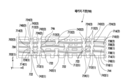
| KR1020247014562A Pending KR20240101796A (ko) | 2021-11-22 | 2022-10-28 | 양면 임베디드 트레이스 기판(ets)을 갖는 패키지 기판을 사용하는 직접 회로(ic) 패키지, 및 관련 제조 방법 |
Country Status (7)
| Country | Link |
|---|---|
| US (1) | US11791320B2 (https=) |
| EP (1) | EP4437586A1 (https=) |
| JP (1) | JP2024541421A (https=) |
| KR (1) | KR20240101796A (https=) |
| CN (1) | CN118284964A (https=) |
| TW (1) | TW202329347A (https=) |
| WO (1) | WO2023091851A1 (https=) |
Families Citing this family (9)
| Publication number | Priority date | Publication date | Assignee | Title |
|---|---|---|---|---|
| US12362269B2 (en) | 2021-10-18 | 2025-07-15 | Qualcomm Incorporated | Integrated circuit (IC) packages employing supplemental metal layer coupled to embedded metal traces in a die-side embedded trace substrate (ETS) layer, and related fabrication methods |
| US11791320B2 (en) * | 2021-11-22 | 2023-10-17 | Qualcomm Incorporated | Integrated circuit (IC) packages employing a package substrate with a double side embedded trace substrate (ETS), and related fabrication methods |
| US12469808B2 (en) * | 2022-08-21 | 2025-11-11 | Taiwan Semiconductor Manufacturing Company, Ltd. | Semiconductor package and manufacturing method thereof |
| US12500197B2 (en) | 2022-12-23 | 2025-12-16 | Deca Technologies Usa, Inc. | Encapsulant-defined land grid array (LGA) package and method for making the same |
| US20250062235A1 (en) * | 2023-08-16 | 2025-02-20 | Qualcomm Incorporated | Package substrate with metallization layer(s) that includes an additional metal pad layer to facilitate reduced via size for reduced bump pitch, and related integrated circuit (ic) packages and fabrication methods |
| US12593709B2 (en) * | 2023-08-17 | 2026-03-31 | Qualcomm Incorporated | Substrate(s) for an integrated circuit (IC) package employing a core layer and an adjacent insulation layer(s) with an embedded metal structure(s) positioned from the core layer |
| US12424450B2 (en) | 2023-11-22 | 2025-09-23 | Deca Technologies Usa, Inc. | Embedded component interposer or substrate comprising displacement compensation traces (DCTs) and method of making the same |
| US12500198B2 (en) | 2024-03-01 | 2025-12-16 | Deca Technologies Usa, Inc. | Quad flat no-lead (QFN) package with tie bars and direct contact interconnect build-up structure and method for making the same |
| US12616038B2 (en) | 2024-07-03 | 2026-04-28 | Deca Technologies Usa, Inc. | Interconnect substrate and method of making |
Family Cites Families (20)
| Publication number | Priority date | Publication date | Assignee | Title |
|---|---|---|---|---|
| US5504992A (en) | 1991-11-29 | 1996-04-09 | Hitachi Chemical Company, Ltd. | Fabrication process of wiring board |
| DE19645854A1 (de) | 1996-11-07 | 1998-05-14 | Hewlett Packard Co | Verfahren zur Herstellung von Leiterplatten |
| US7205483B2 (en) | 2004-03-19 | 2007-04-17 | Matsushita Electric Industrial Co., Ltd. | Flexible substrate having interlaminar junctions, and process for producing the same |
| KR100905566B1 (ko) | 2007-04-30 | 2009-07-02 | 삼성전기주식회사 | 회로 전사용 캐리어 부재, 이를 이용한 코어리스인쇄회로기판, 및 이들의 제조방법 |
| TWI349974B (en) | 2007-07-06 | 2011-10-01 | Unimicron Technology Corp | Structure with embedded circuit |
| KR101654820B1 (ko) | 2008-07-09 | 2016-09-06 | 인벤사스 코포레이션 | 감소된 도전체 공간을 가진 마이크로전자 상호접속 소자, 및 그것을 형성하는 방법 |
| US8288202B2 (en) | 2010-11-22 | 2012-10-16 | STATS ChiPAC, Ltd. | Method of forming partially-etched conductive layer recessed within substrate for bonding to semiconductor die |
| US9508681B2 (en) * | 2014-12-22 | 2016-11-29 | Google Inc. | Stacked semiconductor chip RGBZ sensor |
| US10085342B2 (en) * | 2016-12-13 | 2018-09-25 | Intel Corporation | Microelectronic device having an air core inductor |
| KR102321438B1 (ko) | 2017-07-28 | 2021-11-04 | 엘지이노텍 주식회사 | 인쇄회로기판 |
| EP4181196A3 (en) * | 2017-12-29 | 2023-09-13 | INTEL Corporation | Microelectronic assemblies with communication networks |
| US11348865B2 (en) * | 2019-09-30 | 2022-05-31 | Intel Corporation | Electronic device including a substrate having interconnects |
| US11270991B1 (en) * | 2020-09-02 | 2022-03-08 | Qualcomm Incorporated | Integrated circuits (ICs) employing front side (FS) back end-of-line (BEOL) (FS-BEOL) input/output (I/O) routing and back side (BS) BEOL (BS-BEOL) power routing for current flow organization, and related methods |
| US11552055B2 (en) * | 2020-11-20 | 2023-01-10 | Qualcomm Incorporated | Integrated circuit (IC) packages employing front side back-end-of-line (FS-BEOL) to back side back-end-of-line (BS-BEOL) stacking for three-dimensional (3D) die stacking, and related fabrication methods |
| US11756886B2 (en) * | 2020-12-08 | 2023-09-12 | Intel Corporation | Hybrid manufacturing of microeletronic assemblies with first and second integrated circuit structures |
| US12417978B2 (en) * | 2021-09-09 | 2025-09-16 | Intel Corporation | Microelectronic assemblies having backside die-to-package interconnects |
| US11804645B2 (en) * | 2021-09-14 | 2023-10-31 | Qualcomm Incorporated | Multi-sided antenna module employing antennas on multiple sides of a package substrate for enhanced antenna coverage, and related fabrication methods |
| US12062648B2 (en) * | 2021-09-24 | 2024-08-13 | Qualcomm Incorporated | Multiple (multi-) die integrated circuit (IC) packages for supporting higher connection density, and related fabrication methods |
| US20230114404A1 (en) * | 2021-09-30 | 2023-04-13 | Qualcomm Incorporated | Embedded trace substrate (ets) with embedded metal traces having multiple thickness for integrated circuit (ic) package height control |
| US11791320B2 (en) * | 2021-11-22 | 2023-10-17 | Qualcomm Incorporated | Integrated circuit (IC) packages employing a package substrate with a double side embedded trace substrate (ETS), and related fabrication methods |
-
2021
- 2021-11-22 US US17/456,068 patent/US11791320B2/en active Active
-
2022
- 2022-10-27 TW TW111140827A patent/TW202329347A/zh unknown
- 2022-10-28 WO PCT/US2022/078880 patent/WO2023091851A1/en not_active Ceased
- 2022-10-28 CN CN202280074053.0A patent/CN118284964A/zh active Pending
- 2022-10-28 EP EP22817853.9A patent/EP4437586A1/en active Pending
- 2022-10-28 JP JP2024529645A patent/JP2024541421A/ja active Pending
- 2022-10-28 KR KR1020247014562A patent/KR20240101796A/ko active Pending
Also Published As
| Publication number | Publication date |
|---|---|
| JP2024541421A (ja) | 2024-11-08 |
| CN118284964A (zh) | 2024-07-02 |
| EP4437586A1 (en) | 2024-10-02 |
| WO2023091851A1 (en) | 2023-05-25 |
| US11791320B2 (en) | 2023-10-17 |
| TW202329347A (zh) | 2023-07-16 |
| US20230163112A1 (en) | 2023-05-25 |
Similar Documents
| Publication | Publication Date | Title |
|---|---|---|
| KR20240101796A (ko) | 양면 임베디드 트레이스 기판(ets)을 갖는 패키지 기판을 사용하는 직접 회로(ic) 패키지, 및 관련 제조 방법 | |
| US12354935B2 (en) | Integrated circuit (IC) package substrate with embedded trace substrate (ETS) layer on a substrate, and related fabrication methods | |
| US20230215849A1 (en) | PACKAGE SUBSTRATES WITH EMBEDDED DIE-SIDE, FACE-UP DEEP TRENCH CAPACITOR(S) (DTC(s)), AND RELATED INTEGRATED CIRCUIT (IC) PACKAGES AND FABRICATION METHODS | |
| US12100645B2 (en) | Integrated circuit (IC) package employing added metal for embedded metal traces in ETS-based substrate for reduced signal path impedance, and related fabrication methods | |
| US20230114404A1 (en) | Embedded trace substrate (ets) with embedded metal traces having multiple thickness for integrated circuit (ic) package height control | |
| US20230307336A1 (en) | Package substrates employing pad metallization layer for increased signal routing capacity, and related integrated circuit (ic) packages and fabrication methods | |
| US12362269B2 (en) | Integrated circuit (IC) packages employing supplemental metal layer coupled to embedded metal traces in a die-side embedded trace substrate (ETS) layer, and related fabrication methods | |
| US12525574B2 (en) | Three-dimensional (3D) integrated circuit (IC) (3DIC) package with a bottom die layer employing an extended interposer substrate, and related fabrication methods | |
| US12593709B2 (en) | Substrate(s) for an integrated circuit (IC) package employing a core layer and an adjacent insulation layer(s) with an embedded metal structure(s) positioned from the core layer | |
| US12500146B2 (en) | Substrate(s) for an integrated circuit (IC) package employing a metal core for improved electrical shielding and structural strength, and related IC packages and fabrication methods | |
| US20250239508A1 (en) | Interposer substrate with integrated step die cavity, and related integrated circuit (ic) packages and fabrication methods | |
| US20240250009A1 (en) | EMBEDDED TRACE SUBSTRATES (ETSs) WITH T-SHAPED INTERCONNECTS WITH REDUCED-WIDTH EMBEDDED METAL TRACES, AND RELATED INTEGRATED CIRCUIT (IC) PACKAGES AND FABRICATION METHODS | |
| US12381174B2 (en) | Integrated circuit (IC) packages employing wire bond channel over package substrate, and related fabrication methods | |
| US20260040973A1 (en) | Package substrate with core having metallization layers to facilitate signal routing within the core, and related fabrication methods and integrated circuit (ic) packages | |
| CN117999649A (zh) | 具有用于集成电路(ic)封装高度控制的具有多种厚度的嵌入式金属迹线的嵌入式迹线基板(ets) |
Legal Events
| Date | Code | Title | Description |
|---|---|---|---|
| PA0105 | International application |
St.27 status event code: A-0-1-A10-A15-nap-PA0105 |
|
| PG1501 | Laying open of application |
St.27 status event code: A-1-1-Q10-Q12-nap-PG1501 |
|
| P22-X000 | Classification modified |
St.27 status event code: A-2-2-P10-P22-nap-X000 |