KR20220110065A - Peeling apparatus - Google Patents
Peeling apparatus Download PDFInfo
- Publication number
- KR20220110065A KR20220110065A KR1020210184242A KR20210184242A KR20220110065A KR 20220110065 A KR20220110065 A KR 20220110065A KR 1020210184242 A KR1020210184242 A KR 1020210184242A KR 20210184242 A KR20210184242 A KR 20210184242A KR 20220110065 A KR20220110065 A KR 20220110065A
- Authority
- KR
- South Korea
- Prior art keywords
- ingot
- peeling
- wafer
- ultrasonic
- sic ingot
- Prior art date
Links
Images


Classifications
-
- B—PERFORMING OPERATIONS; TRANSPORTING
- B23—MACHINE TOOLS; METAL-WORKING NOT OTHERWISE PROVIDED FOR
- B23K—SOLDERING OR UNSOLDERING; WELDING; CLADDING OR PLATING BY SOLDERING OR WELDING; CUTTING BY APPLYING HEAT LOCALLY, e.g. FLAME CUTTING; WORKING BY LASER BEAM
- B23K26/00—Working by laser beam, e.g. welding, cutting or boring
- B23K26/36—Removing material
- B23K26/38—Removing material by boring or cutting
-
- B—PERFORMING OPERATIONS; TRANSPORTING
- B28—WORKING CEMENT, CLAY, OR STONE
- B28D—WORKING STONE OR STONE-LIKE MATERIALS
- B28D5/00—Fine working of gems, jewels, crystals, e.g. of semiconductor material; apparatus or devices therefor
- B28D5/04—Fine working of gems, jewels, crystals, e.g. of semiconductor material; apparatus or devices therefor by tools other than rotary type, e.g. reciprocating tools
-
- B—PERFORMING OPERATIONS; TRANSPORTING
- B23—MACHINE TOOLS; METAL-WORKING NOT OTHERWISE PROVIDED FOR
- B23K—SOLDERING OR UNSOLDERING; WELDING; CLADDING OR PLATING BY SOLDERING OR WELDING; CUTTING BY APPLYING HEAT LOCALLY, e.g. FLAME CUTTING; WORKING BY LASER BEAM
- B23K26/00—Working by laser beam, e.g. welding, cutting or boring
- B23K26/50—Working by transmitting the laser beam through or within the workpiece
- B23K26/53—Working by transmitting the laser beam through or within the workpiece for modifying or reforming the material inside the workpiece, e.g. for producing break initiation cracks
-
- H—ELECTRICITY
- H01—ELECTRIC ELEMENTS
- H01L—SEMICONDUCTOR DEVICES NOT COVERED BY CLASS H10
- H01L21/00—Processes or apparatus adapted for the manufacture or treatment of semiconductor or solid state devices or of parts thereof
- H01L21/02—Manufacture or treatment of semiconductor devices or of parts thereof
- H01L21/04—Manufacture or treatment of semiconductor devices or of parts thereof the devices having at least one potential-jump barrier or surface barrier, e.g. PN junction, depletion layer or carrier concentration layer
- H01L21/18—Manufacture or treatment of semiconductor devices or of parts thereof the devices having at least one potential-jump barrier or surface barrier, e.g. PN junction, depletion layer or carrier concentration layer the devices having semiconductor bodies comprising elements of Group IV of the Periodic System or AIIIBV compounds with or without impurities, e.g. doping materials
- H01L21/26—Bombardment with radiation
- H01L21/263—Bombardment with radiation with high-energy radiation
- H01L21/268—Bombardment with radiation with high-energy radiation using electromagnetic radiation, e.g. laser radiation
-
- B—PERFORMING OPERATIONS; TRANSPORTING
- B23—MACHINE TOOLS; METAL-WORKING NOT OTHERWISE PROVIDED FOR
- B23K—SOLDERING OR UNSOLDERING; WELDING; CLADDING OR PLATING BY SOLDERING OR WELDING; CUTTING BY APPLYING HEAT LOCALLY, e.g. FLAME CUTTING; WORKING BY LASER BEAM
- B23K26/00—Working by laser beam, e.g. welding, cutting or boring
- B23K26/14—Working by laser beam, e.g. welding, cutting or boring using a fluid stream, e.g. a jet of gas, in conjunction with the laser beam; Nozzles therefor
- B23K26/146—Working by laser beam, e.g. welding, cutting or boring using a fluid stream, e.g. a jet of gas, in conjunction with the laser beam; Nozzles therefor the fluid stream containing a liquid
-
- B—PERFORMING OPERATIONS; TRANSPORTING
- B28—WORKING CEMENT, CLAY, OR STONE
- B28D—WORKING STONE OR STONE-LIKE MATERIALS
- B28D5/00—Fine working of gems, jewels, crystals, e.g. of semiconductor material; apparatus or devices therefor
- B28D5/04—Fine working of gems, jewels, crystals, e.g. of semiconductor material; apparatus or devices therefor by tools other than rotary type, e.g. reciprocating tools
- B28D5/047—Fine working of gems, jewels, crystals, e.g. of semiconductor material; apparatus or devices therefor by tools other than rotary type, e.g. reciprocating tools by ultrasonic cutting
-
- B—PERFORMING OPERATIONS; TRANSPORTING
- B28—WORKING CEMENT, CLAY, OR STONE
- B28D—WORKING STONE OR STONE-LIKE MATERIALS
- B28D7/00—Accessories specially adapted for use with machines or devices of the preceding groups
-
- H—ELECTRICITY
- H01—ELECTRIC ELEMENTS
- H01L—SEMICONDUCTOR DEVICES NOT COVERED BY CLASS H10
- H01L21/00—Processes or apparatus adapted for the manufacture or treatment of semiconductor or solid state devices or of parts thereof
- H01L21/02—Manufacture or treatment of semiconductor devices or of parts thereof
- H01L21/04—Manufacture or treatment of semiconductor devices or of parts thereof the devices having at least one potential-jump barrier or surface barrier, e.g. PN junction, depletion layer or carrier concentration layer
- H01L21/18—Manufacture or treatment of semiconductor devices or of parts thereof the devices having at least one potential-jump barrier or surface barrier, e.g. PN junction, depletion layer or carrier concentration layer the devices having semiconductor bodies comprising elements of Group IV of the Periodic System or AIIIBV compounds with or without impurities, e.g. doping materials
- H01L21/30—Treatment of semiconductor bodies using processes or apparatus not provided for in groups H01L21/20 - H01L21/26
- H01L21/302—Treatment of semiconductor bodies using processes or apparatus not provided for in groups H01L21/20 - H01L21/26 to change their surface-physical characteristics or shape, e.g. etching, polishing, cutting
- H01L21/304—Mechanical treatment, e.g. grinding, polishing, cutting
-
- B—PERFORMING OPERATIONS; TRANSPORTING
- B23—MACHINE TOOLS; METAL-WORKING NOT OTHERWISE PROVIDED FOR
- B23K—SOLDERING OR UNSOLDERING; WELDING; CLADDING OR PLATING BY SOLDERING OR WELDING; CUTTING BY APPLYING HEAT LOCALLY, e.g. FLAME CUTTING; WORKING BY LASER BEAM
- B23K2103/00—Materials to be soldered, welded or cut
- B23K2103/50—Inorganic material, e.g. metals, not provided for in B23K2103/02 – B23K2103/26
- B23K2103/56—Inorganic material, e.g. metals, not provided for in B23K2103/02 – B23K2103/26 semiconducting
Abstract
Description
본 발명은, 박리 장치에 관한 것이다.The present invention relates to a peeling device.
디바이스가 형성되는 웨이퍼는, 일반적으로 원기둥 형상의 반도체 잉곳을 와이어 소로 얇게 절단하고, 절단 후에 웨이퍼의 표리면을 연마함으로써 제조된다.The wafer on which a device is formed is manufactured by generally cutting|disconnecting a cylindrical semiconductor ingot thinly with a wire saw, and grinding|polishing the front and back surfaces of a wafer after cutting.
그러나, 상기 서술한 방법으로 웨이퍼를 제조하면, 반도체 잉곳의 대부분 (체적의 70 % ∼ 80 %) 이 제거에 의해 버려지게 되기 때문에, 경제적이지 않다는 문제가 있다.However, when a wafer is manufactured by the above-mentioned method, since most (70% to 80% of a volume) of a semiconductor ingot will be discarded by removal, there exists a problem that it is not economical.
특히, 최근 파워 디바이스로서 주목받고 있는 SiC 에 의해 구성되는 SiC 잉곳은, 경도가 높아 와이어 소에 의한 절단이 곤란하기 때문에, 절단에 시간이 걸려 생산성이 나쁘다는 과제가 존재하고 있다.In particular, since the SiC ingot comprised of SiC attracting attention as a power device in recent years has high hardness and cutting|disconnection with a wire saw is difficult, cutting takes time and the subject that productivity is bad exists.
그래서, 본 출원인들은, 단결정의 SiC 잉곳에 대해 투과성을 갖는 파장의 레이저 빔의 집광점을 SiC 잉곳의 내부에 위치시켜 집광 조사하여, 절단 예정면에 박리층을 형성하는 기술이나, 박리층을 형성한 SiC 잉곳에 대해 초음파를 부여함으로써 박리층을 기점으로 하여 웨이퍼를 분리·제조하는 기술을 제안하였다 (예를 들어, 특허문헌 1 및 특허문헌 2 참조).Therefore, the present applicants have developed a technique of forming a peeling layer on a surface to be cut by irradiating a focused point of a laser beam having a wavelength that is transparent to a single crystal SiC ingot by locating it inside the SiC ingot, or forming a peeling layer A technique of separating and manufacturing a wafer from the release layer as a starting point by applying ultrasonic waves to one SiC ingot has been proposed (see, for example,
여기서, SiC 잉곳에 대해 초음파를 부여하기 위해서는, 초음파를 조사하고자 하는 영역과 동등 혹은 그 이상의 면적의 단면 (端面) 을 갖는 초음파 부여 수단이 필요해진다. 따라서, 현 상황에서는, 초음파 진동자에 진동판을 접착함으로써 원하는 면적을 갖는 단면을 형성하고 있다.Here, in order to apply ultrasonic waves to the SiC ingot, an ultrasonic wave imparting means having a cross section having an area equal to or greater than the area to be irradiated with ultrasonic waves is required. Accordingly, in the present situation, a cross section having a desired area is formed by bonding the diaphragm to the ultrasonic vibrator.
그런데, 초음파 진동자와 진동판을 접착시키고 있는 접착제가 장시간의 사용에 수반하여 박리되어 버려, 특성 변동이 생기기 때문에, 효율적인 웨이퍼의 제조를 할 수 없게 된다는 문제가 명백해졌다.However, since the adhesive bonding the ultrasonic vibrator and the diaphragm is peeled off with long-term use, and a characteristic variation occurs, the problem that efficient wafer production cannot be performed has become apparent.
따라서, 본 발명의 목적은, 특성 변동을 억제하면서 효율적으로 반도체 잉곳으로부터 웨이퍼를 제조하는 것이 가능한 박리 장치를 제공하는 것이다.Accordingly, it is an object of the present invention to provide a peeling apparatus capable of efficiently manufacturing a wafer from a semiconductor ingot while suppressing characteristic fluctuations.
본 발명에 의하면, 반도체 잉곳에 대해 투과성을 갖는 파장의 레이저 빔의 집광점을 제조해야 하는 웨이퍼의 두께에 상당하는 깊이에 위치시켜 레이저 빔을 조사하여 박리층을 형성한 반도체 잉곳으로부터, 제조해야 하는 웨이퍼를 박리하는 박리 장치로서, 제조해야 하는 웨이퍼를 위로 하여 반도체 잉곳을 유지하는 잉곳 유지 유닛과, 그 잉곳 유지 유닛에 유지된 반도체 잉곳과 대면하도록 배치 형성되고, 초음파를 발진시키는 초음파 발진 유닛과, 제조해야 하는 웨이퍼와 그 초음파 발진 유닛 사이에 액체를 공급하는 액체 공급 유닛을 포함하고, 그 초음파 발진 유닛은, 초음파 진동자와, 초음파를 부여하고자 하는 면적과 동등 혹은 그 이상의 면적을 갖도록 형성된 바닥면을 갖는 케이스 부재를 포함하고, 그 케이스 부재는, 그 초음파 진동자의 단면과 일체화되어 형성되어 있는 박리 장치가 제공된다.According to the present invention, the converging point of the laser beam of a wavelength having transparency to the semiconductor ingot is located at a depth corresponding to the thickness of the wafer to be manufactured, and the laser beam is irradiated to form a peeling layer from the semiconductor ingot to be manufactured. A peeling apparatus for peeling a wafer, comprising: an ingot holding unit for holding a semiconductor ingot with a wafer to be manufactured facing up; a liquid supply unit for supplying a liquid between a wafer to be manufactured and the ultrasonic oscillation unit, the ultrasonic oscillation unit comprising an ultrasonic vibrator and a bottom surface formed to have an area equal to or greater than an area to which an ultrasonic wave is to be applied There is provided a peeling device including a case member having a case member, the case member being integrally formed with an end face of the ultrasonic vibrator.
바람직하게는, 그 케이스 부재는, 스테인리스강, 티탄, 알루미늄 중 어느 것을 포함하고 있다.Preferably, the case member contains any of stainless steel, titanium, and aluminum.
본 발명에 의하면, 특성 변동을 억제하면서 효율적으로 반도체 잉곳으로부터 웨이퍼를 제조하는 것이 가능해진다는 효과를 발휘한다.ADVANTAGE OF THE INVENTION According to this invention, it exhibits the effect that it becomes possible to manufacture a wafer from a semiconductor ingot efficiently, suppressing a characteristic fluctuation|variation.
도 1 은, 제 1 실시형태에 관련된 박리 장치의 가공 대상의 SiC 잉곳의 평면도이다.
도 2 는, 도 1 에 나타낸 SiC 잉곳의 측면도이다.
도 3 은, 제 1 실시형태에 관련된 박리 장치에 의해 제조되는 웨이퍼의 사시도이다.
도 4 는, 도 1 에 나타낸 SiC 잉곳에 박리층이 형성된 상태의 평면도이다.
도 5 는, 도 4 중의 V-V 선을 따른 단면도이다.
도 6 은, 도 1 에 나타낸 SiC 잉곳에 박리층을 형성하는 상태를 나타내는 사시도이다.
도 7 은, 도 6 에 나타낸 SiC 잉곳에 박리층을 형성하는 상태를 나타내는 측면도이다.
도 8 은, 제 1 실시형태에 관련된 박리 장치의 구성예를 나타내는 측면도이다.
도 9 는, 도 8 에 나타낸 박리 장치의 초음파 발진 유닛의 측단면도이다.
도 10 은, 제 2 실시형태에 관련된 박리 장치의 구성예를 나타내는 측면도이다.BRIEF DESCRIPTION OF THE DRAWINGS It is a top view of the SiC ingot to be processed by the peeling apparatus which concerns on 1st Embodiment.
FIG. 2 is a side view of the SiC ingot shown in FIG. 1 .
3 is a perspective view of a wafer manufactured by the peeling apparatus according to the first embodiment.
4 : is a top view of the state in which the peeling layer was formed in the SiC ingot shown in FIG.
FIG. 5 is a cross-sectional view taken along line VV in FIG. 4 .
FIG. 6 : is a perspective view which shows the state which forms a peeling layer in the SiC ingot shown in FIG.
It is a side view which shows the state which forms a peeling layer in the SiC ingot shown in FIG.
It is a side view which shows the structural example of the peeling apparatus which concerns on 1st Embodiment.
Fig. 9 is a side cross-sectional view of an ultrasonic oscillation unit of the peeling apparatus shown in Fig. 8;
It is a side view which shows the structural example of the peeling apparatus which concerns on 2nd Embodiment.
이하, 본 발명의 실시형태에 대해, 도면을 참조하면서 상세하게 설명한다. 이하의 실시형태에 기재한 내용에 의해 본 발명이 한정되는 것은 아니다. 또, 이하에 기재한 구성 요소에는, 당업자가 용이하게 상정할 수 있는 것, 실질적으로 동일한 것이 포함된다. 또한, 이하에 기재한 구성은 적절히 조합하는 것이 가능하다. 또, 본 발명의 요지를 일탈하지 않는 범위에서 구성의 여러 가지 생략, 치환 또는 변경을 실시할 수 있다.EMBODIMENT OF THE INVENTION Hereinafter, embodiment of this invention is described in detail, referring drawings. This invention is not limited by the content described in the following embodiment. In addition, the components described below include those that can be easily assumed by those skilled in the art, and those that are substantially the same. In addition, the structures described below can be combined suitably. In addition, various omissions, substitutions, or changes in the configuration can be made without departing from the gist of the present invention.
〔제 1 실시형태〕[First Embodiment]
본 발명의 제 1 실시형태에 관련된 박리 장치를 도면에 기초하여 설명한다. 먼저, 제 1 실시형태에 관련된 박리 장치의 가공 대상의 잉곳인 SiC 잉곳을 설명한다. 도 1 은, 제 1 실시형태에 관련된 박리 장치의 가공 대상의 SiC 잉곳의 평면도이다. 도 2 는, 도 1 에 나타낸 SiC 잉곳의 측면도이다. 도 3 은, 제 1 실시형태에 관련된 박리 장치에 의해 제조되는 웨이퍼의 사시도이다. 도 4 는, 도 1 에 나타낸 SiC 잉곳에 박리층이 형성된 상태의 평면도이다. 도 5 는, 도 4 중의 V-V 선을 따른 단면도이다. 도 6 은, 도 1 에 나타낸 SiC 잉곳에 박리층을 형성하는 상태를 나타내는 사시도이다. 도 7 은, 도 6 에 나타낸 SiC 잉곳에 박리층을 형성하는 상태를 나타내는 측면도이다.The peeling apparatus which concerns on 1st Embodiment of this invention is demonstrated based on drawing. First, the SiC ingot which is the ingot of the process object of the peeling apparatus which concerns on 1st Embodiment is demonstrated. BRIEF DESCRIPTION OF THE DRAWINGS It is a top view of the SiC ingot to be processed by the peeling apparatus which concerns on 1st Embodiment. FIG. 2 is a side view of the SiC ingot shown in FIG. 1 . 3 is a perspective view of a wafer manufactured by the peeling apparatus according to the first embodiment. 4 : is a top view of the state in which the peeling layer was formed in the SiC ingot shown in FIG. FIG. 5 is a cross-sectional view taken along line V-V in FIG. 4 . FIG. 6 : is a perspective view which shows the state which forms a peeling layer in the SiC ingot shown in FIG. It is a side view which shows the state which forms a peeling layer in the SiC ingot shown in FIG.
(SiC 잉곳) (SiC ingot)
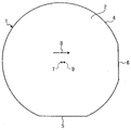
도 1 및 도 2 에 나타내는 SiC 잉곳 (1) 은, 제 1 실시형태에서는, SiC (탄화규소) 로 이루어지고, 전체적으로 원기둥상으로 형성되어 있다. 제 1 실시형태에 있어서, SiC 잉곳 (1) 은, 육방정 단결정 SiC 잉곳이다.The
SiC 잉곳 (1) 은, 도 1 및 도 2 에 나타내는 바와 같이, 원 형상의 단면인 제 1 면 (2) 과, 제 1 면 (2) 의 이면측의 원 형상의 제 2 면 (3) 과, 제 1 면 (2) 의 외측 가장자리와 제 2 면 (3) 의 외측 가장자리에 연결되는 둘레면 (4) 을 가지고 있다. 또, SiC 잉곳 (1) 은, 둘레면 (4) 에 결정 방위를 나타내는 제 1 오리엔테이션 플랫 (5) 과, 제 1 오리엔테이션 플랫 (5) 에 직교하는 제 2 오리엔테이션 플랫 (6) 을 가지고 있다. 제 1 오리엔테이션 플랫 (5) 의 길이는 제 2 오리엔테이션 플랫 (6) 의 길이보다 길다.The
또, SiC 잉곳 (1) 은, 제 1 면 (2) 의 수직선 (7) 에 대해 제 2 오리엔테이션 플랫 (6) 을 향하는 경사 방향 (8) 에 오프각 (α) 경사진 c 축 (9) 과 c 축 (9) 에 직교하는 c 면 (10) 을 가지고 있다. c 면 (10) 은, SiC 잉곳 (1) 의 제 1 면 (2) 에 대해 오프각 (α) 경사져 있다. c 축 (9) 의 수직선 (7) 으로부터의 경사 방향 (8) 은, 제 2 오리엔테이션 플랫 (6) 의 신장 방향에 직교하고, 또한 제 1 오리엔테이션 플랫 (5) 과 평행하다. c 면 (10) 은, SiC 잉곳 (1) 중에 SiC 잉곳 (1) 의 분자 레벨에서 무수하게 설정된다. 제 1 실시형태에서는, 오프각 (α) 은, 1°, 4°또는 6°로 설정되어 있지만, 본 발명에서는, 오프각 (α) 을 예를 들어 1° ∼ 6°의 범위에서 자유롭게 설정하여 SiC 잉곳 (1) 을 제조할 수 있다.In addition, the
또, SiC 잉곳 (1) 은, 제 1 면 (2) 이 연삭 장치에 의해 연삭 가공된 후, 연마 장치에 의해 연마 가공되어, 제 1 면 (2) 이 경면으로 형성된다. SiC 잉곳 (1) 은, 제 1 면 (2) 측의 일부분이 박리되고, 박리된 일부분이 도 3 에 나타내는 웨이퍼 (20) 로 제조되는 것이다.Moreover, as for the
도 3 에 나타내는 웨이퍼 (20) 는, SiC 잉곳 (1) 의 일부분이 박리되고, SiC 잉곳 (1) 으로부터 박리된 면 (21) 에 연삭 가공, 연마 가공 등이 실시되어 제조된다. 웨이퍼 (20) 는, SiC 잉곳 (1) 으로부터 박리된 후, 표면에 디바이스가 형성된다. 제 1 실시형태에서는, 디바이스는, MOSFET (Metal-oxide-semiconductor Field-effect Transistor), MEMS (Micro Electro Mechanical Systems) 또는 SBD (Schottky Barrier Diode) 이지만, 본 발명에서는, 디바이스는, MOSFET, MEMS 및 SBD 에 한정되지 않는다. 또한, 웨이퍼 (20) 의 SiC 잉곳 (1) 과 동일 부분에 동일 부호를 붙여 설명을 생략한다.As for the
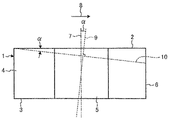
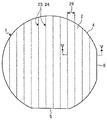
도 1 및 도 2 에 나타내는 SiC 잉곳 (1) 은, 도 4 및 도 5 에 나타내는 박리층 (23) 이 형성된 후, 박리층 (23) 을 기점으로 일부분, 즉 제조해야 하는 웨이퍼 (20) 가 분리, 박리된다. 박리층 (23) 은, SiC 잉곳 (1) 의 제 2 면 (3) 측이 레이저 가공 장치 (30) (도 6 및 도 7 에 나타낸다) 의 유지 테이블 (31) 에 흡인 유지되고, 레이저 가공 장치 (30) 에 의해 형성된다. 레이저 가공 장치 (30) 는, SiC 잉곳 (1) 에 대해 투과성을 갖는 파장의 펄스상의 레이저 빔 (32) (도 7 에 나타낸다) 의 집광점 (33) 을 SiC 잉곳 (1) 의 제 1 면 (2) 으로부터 제조해야 하는 웨이퍼 (20) 의 두께 (22) (도 3 에 나타낸다) 에 상당하는 깊이 (35) (도 5및 도 7 에 나타낸다) 에 위치시키고, 제 2 오리엔테이션 플랫 (6) 을 따라 펄스상의 레이저 빔 (32) 을 조사하여, SiC 잉곳 (1) 의 내부에 박리층 (23) 을 형성한다.In the
SiC 잉곳 (1) 은, SiC 잉곳 (1) 에 대해 투과성을 갖는 파장의 펄스상의 레이저 빔 (32) 이 조사되면, 도 5 에 나타내는 바와 같이, 펄스상의 레이저 빔 (32) 의 조사에 의해 SiC 가 Si (실리콘) 와 C (탄소) 로 분리되고 다음으로 조사되는 펄스상의 레이저 빔 (32) 이 전에 형성된 C 에 흡수되어 연쇄적으로 SiC 가 Si 와 C 로 분리되는 개질부 (24) 가, X 축 방향을 따라 SiC 잉곳 (1) 의 내부에 형성됨과 함께, 개질부 (24) 로부터 c 면 (10) 을 따라 연장되는 크랙 (25) 이 제조된다. 이렇게 하여, SiC 잉곳 (1) 은, SiC 잉곳 (1) 에 대해 투과성을 갖는 파장의 펄스상의 레이저 빔 (32) 이 조사되면, 개질부 (24) 와, 개질부 (24) 로부터 c 면 (10) 을 따라 형성되는 크랙 (25) 을 포함하는 박리층 (23) 을 형성한다.When the
레이저 가공 장치 (30) 는, 박리층 (23) 을 형성할 때에, SiC 잉곳 (1) 의 제 2 오리엔테이션 플랫 (6) 과 평행한 방향의 전체 길이에 걸쳐 레이저 빔 (32) 을 조사하면, SiC 잉곳 (1) 과 레이저 빔 (32) 을 조사하는 레이저 빔 조사 유닛 (36) 을 제 1 오리엔테이션 플랫 (5) 을 따라 상대적으로 인덱스 이송한다.When the
레이저 가공 장치 (30) 는, 재차, 집광점 (33) 을 제 1 면 (2) 으로부터 원하는 깊이에 위치시키고, 제 2 오리엔테이션 플랫 (6) 을 따라 펄스상의 레이저 빔 (32) 을 SiC 잉곳 (1) 에 조사하여, SiC 잉곳 (1) 의 내부에 박리층 (23) 을 형성한다. 레이저 가공 장치 (30) 는, 레이저 빔 (32) 을 제 2 오리엔테이션 플랫 (6) 을 따라 조사하는 동작과, 레이저 빔 조사 유닛을 제 1 오리엔테이션 플랫 (5) 을 따라 상대적으로 인덱스 이송되는 동작을 반복한다.The
이로써, SiC 잉곳 (1) 은, 인덱스 이송의 이동 거리 (26) 마다, 제 1 면 (2) 으로부터 웨이퍼 (20) 의 두께 (22) 에 상당하는 깊이 (35) 에, SiC 가 Si 와 C 로 분리된 개질부 (24) 와 크랙 (25) 을 포함하는 다른 부분보다 강도가 저하된 박리층 (23) 이 형성된다. SiC 잉곳 (1) 은, 제 1 면 (2) 으로부터 웨이퍼 (20) 의 두께 (22) 에 상당하는 깊이 (35) 에, 제 1 오리엔테이션 플랫 (5) 과 평행한 방향의 전체 길이에 걸쳐 인덱스 이송의 이동 거리마다 박리층 (23) 이 형성된다.In this way, the
(박리 장치)(Peeling Device)
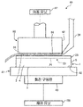
다음으로, 박리 장치를 설명한다. 도 8 은, 제 1 실시형태에 관련된 박리 장치의 구성예를 나타내는 측면도이다. 도 9 는, 도 8 에 나타낸 박리 장치의 초음파 발진 유닛의 측단면도이다. 제 1 실시형태에 관련된 박리 장치 (40) 는, 도 4 및 도 5 에 나타내는 박리층 (23) 을 형성한 SiC 잉곳 (1) 으로부터 도 4 에 나타내는 제조해야 하는 웨이퍼 (20) 를 박리하는 박리 장치이다.Next, a peeling apparatus is demonstrated. It is a side view which shows the structural example of the peeling apparatus which concerns on 1st Embodiment. Fig. 9 is a side cross-sectional view of an ultrasonic oscillation unit of the peeling apparatus shown in Fig. 8; The peeling
박리 장치 (40) 는, SiC 잉곳 (1) 에 대해 투과성을 갖는 파장의 레이저 빔 (32) 의 집광점 (33) 을 제조해야 하는 웨이퍼 (20) 의 두께 (22) 에 상당하는 깊이 (35) 에 위치시키고 레이저 빔 (32) 을 조사하여 박리층 (23) 을 형성한 SiC 잉곳 (1) 으로부터, 제조해야 하는 웨이퍼 (20) 를 박리하는 장치이다. 박리 장치 (40) 는, 도 8 에 나타내는 바와 같이, 잉곳 유지 유닛 (41) 과, 액체 공급 유닛 (50) 과, 초음파 발진 유닛 (60) 과, 제어 유닛 (100) 을 포함한다.The peeling
잉곳 유지 유닛 (41) 은, 제조해야 하는 웨이퍼 (20) 를 위로 하여 SiC 잉곳 (1) 을 유지하는 것이다. 잉곳 유지 유닛 (41) 은, 두꺼운 원반상으로 형성되어 있다. 잉곳 유지 유닛 (41) 은, 상면이 수평 방향과 평행한 유지면 (42) 으로서, 유지면 (42) 상에 SiC 잉곳 (1) 의 제 2 면 (3) 이 재치 (載置) 되고, 제 1 면 (2) 을 상방을 향하게 하여, SiC 잉곳 (1) 을 유지한다. 제 1 실시형태에서는, 잉곳 유지 유닛 (41) 은, 유지면 (42) 에 SiC 잉곳 (1) 의 제 2 면 (3) 을 흡인 유지한다 (즉, 배큐엄 고정시킨다). 또, 잉곳 유지 유닛 (41) 은, 유지면 (42) 에 SiC 잉곳 (1) 을 유지한 상태에서 회전 구동원 (43) 에 의해 축심 둘레로 회전된다.The
액체 공급 유닛 (50) 은, 제조해야 하는 웨이퍼 (20) 와 초음파 발진 유닛 (60) 사이에 액체 (51) (도 8 에 나타낸다) 를 공급하는 것이다. 액체 공급 유닛 (50) 은, 액체 공급원으로부터 공급된 액체 (51) 를 하단으로부터 공급하는 관으로서, 제 1 실시형태에서는, 잉곳 유지 유닛 (41) 에 유지된 SiC 잉곳 (1) 의 제 1 면 (2) 상에 액체 (51) 를 공급한다. 또, 제 1 실시형태에서는, 액체 공급 유닛 (50) 은, 도시되지 않은 승강 기구에 의해 자유롭게 승강할 수 있도록 형성되어 있다.The
초음파 발진 유닛 (60) 은, 잉곳 유지 유닛 (41) 에 유지된 SiC 잉곳 (1) 과 대면하도록 배치 형성되고, 초음파를 발진시키는 것이다. 초음파 발진 유닛 (60) 은, 도 9 에 나타내는 바와 같이, 케이스 부재 (61) 와, 초음파 진동자 (70) 를 구비한다.The
케이스 부재 (61) 는, 상부에 개구를 형성한 상자형의 케이스 본체 (62) 와, 평판상의 덮개체 (63) 를 구비한다. 케이스 본체 (62) 는, 금속에 의해 구성되고, 잉곳 유지 유닛 (41) 에 유지된 SiC 잉곳 (1) 의 제 1 면 (2) 과 대향하는 바닥면 (64) 을 갖는 원판상의 바닥면부 (65) 와, 바닥면부 (65) 의 외측 가장자리로부터 세워 형성한 원통상의 원통부 (66) 를 일체로 구비하고 있다. 또, 본 발명에서는, 케이스 부재 (61) 는, 초음파 진동자 (70) 가 예를 들어 6 개 사용되어, 바닥면부 (65) 가 타원 형상으로 구성되어도 된다. 본 발명에서는, 케이스 부재 (61) 는, 바닥면부 (65) 가 정방형이나 장방형으로 구성되면, 장소에 따라 초음파 진동자 (70) 로부터 케이스 부재 (61) 까지의 거리가 변함으로써 박리성에 영향을 미칠 가능성이 있기 때문에, 초음파 진동자 (70) 로부터 케이스 부재 (61) 의 바닥면부 (65) 까지의 거리를 가능한 한 동등하게 하기 위해서, 바닥면부 (65) 가 원판상이나 타원 형상으로 구성되는 것이 바람직하다.The
케이스 본체 (62) 의 바닥면부 (65) 의 바닥면 (64) 은, 초음파 발진 유닛 (60) 이 초음파를 부여하고자 하는 SiC 잉곳 (1) 의 제 1 면 (2) 의 면적과 동등 혹은 그 이상의 면적을 갖도록 형성되어 있다. 즉, 케이스 부재 (61) 는, 초음파 발진 유닛 (60) 이 초음파를 부여하고자 하는 SiC 잉곳 (1) 의 제 1 면 (2) 의 면적과 동등 혹은 그 이상의 면적을 갖는 바닥면 (64) 을 가지고 있다.The
본 발명에 있어서, 초음파를 부여하고자 하는 SiC 잉곳 (1) 의 제 1 면 (2) 의 면적과 동등 혹은 그 이상의 면적을 갖는다란, 케이스 본체 (62) 의 바닥면 (64) 의 면적이, 잉곳 유지 유닛 (41) 에 유지된 초음파를 부여하고자 하는 SiC 잉곳 (1) 의 제 1 면 (2) 의 면적의 50 % 이상이고 또한 150 % 이하의 면적인 것을 나타내고 있다.In the present invention, when the area of the
바닥면 (64) 의 면적이, 제 1 면 (2) 의 면적의 50 % 미만이면, 초음파 발진 유닛 (60) 을 X 축 방향으로 요동시킴으로써, SiC 잉곳 (1) 으로부터 제조해야 하는 웨이퍼 (20) 를 박리하는 것이 가능하지만, 웨이퍼 (20) 를 SiC 잉곳 (1) 으로부터 박리하기까지 걸리는 소요 시간이 장시간화되어 버리기 때문이다. 또, 바닥면 (64) 의 면적이, 제 1 면 (2) 의 면적의 150 % 를 초과하면, 박리 장치 (40) 전체가 지나치게 대형화되어 바람직하지 않음과 함께, 액체 공급 유닛 (50) 이 SiC 잉곳 (1) 의 제조해야 하는 웨이퍼 (20) 와 초음파 발진 유닛 (60) 의 바닥면 (64) 사이에 액체를 공급하는 것이 곤란해지기 때문이다. 제 1 실시형태에서는, 바닥면 (64) 의 면적은, 제 1 면 (2) 의 면적의 80 % 이다.When the area of the
덮개체 (63) 는, 외경이 바닥면 (64) 의 외경과 동등한 원판상으로 형성되어 있다. 덮개체 (63) 는, 외측 가장자리가 원통부 (66) 의 외측 가장자리에 고정되고, 케이스 본체 (62) 의 개구를 폐색한다.The
초음파 진동자 (70) 는, 초음파를 발진시키는 것이다. 제 1 실시형태에 있어서, 초음파 발진 유닛 (60) 은, 초음파 진동자 (70) 를 복수 구비하고 있다. 복수의 초음파 진동자 (70) 는, 케이스 부재 (61) 내에 수용되고, 서로 간격을 두고 배치되어 있음과 함께, 케이스 본체 (62) 의 바닥면부 (65) 에 고정되어 있다.The
초음파 진동자 (70) 는, 원환상의 피에조 소자 (71) 와, 원통상의 제 1 금속 블록 (72) 과, 제 2 금속 블록 (73) 과, 고정용의 볼트 (75) 를 구비하고 있다.The
초음파 진동자 (70) 는, 제 1 실시형태에서는, 피에조 소자 (71) 를 2 개 구비하고 있다. 2 개의 피에조 소자 (71) 는, 축심 방향으로 서로 중첩되어 있다. 피에조 소자 (71) 는, 교류 전력이 인가되면 두께 방향으로 신축되는 티탄산지르콘산납에 의해 구성되어 있다.The
제 1 금속 블록 (72) 은, 금속에 의해 구성되고, 일방의 피에조 소자 (71) 에 중첩되어 있다. 제 2 금속 블록 (73) 은, 금속에 의해 구성되고, 타방의 피에조 소자 (71) 에 중첩되어 있다. 제 2 금속 블록 (73) 은, 타방의 피에조 소자 (71) 로부터 멀어짐에 따라 외형이 커지는 재두 (裁頭) 원추상으로 형성되어 있다. 제 2 금속 블록 (73) 은, 타방의 피에조 소자 (71) 에 중첩되는 단면 (731) 에 볼트 (75) 가 나사 결합하는 나사공 (732) 이 개구되어 있다.The
볼트 (75) 는, 제 1 금속 블록 (72), 일방의 피에조 소자 (71), 타방의 피에조 소자 (71) 의 내측에 통과되고, 제 2 금속 블록 (73) 의 나사공 (732) 에 나사 결합한다. 볼트 (75) 는, 나사공 (732) 에 나사 결합하면, 제 1 금속 블록 (72), 일방의 피에조 소자 (71), 타방의 피에조 소자 (71) 및 제 2 금속 블록 (73) 을 서로 고정시킨다.The
또, 제 1 실시형태에 있어서, 볼트 (75) 에 의해 고정된 제 1 금속 블록 (72), 일방의 피에조 소자 (71), 타방의 피에조 소자 (71) 및 제 2 금속 블록 (73) 은, 서로 동축이 되는 위치에 배치된다. 또, 제 1 실시형태에 있어서, 초음파 진동자 (70) 는, 피에조 소자 (71) 사이와, 타방의 피에조 소자 (71) 와 제 2 금속 블록 (73) 사이에, 피에조 소자 (71) 에 교류 전력을 인가하는 전극 (74) 을 형성하고 있다. 전극 (74) 은, 교류 전력을 공급하는 도시되지 않은 교류 전원과 전기적으로 접속되어 있다. 초음파 발진 유닛 (60) 은, 전극에 교류 전력이 인가되어, 피에조 소자 (71) 가 신축되면, 전체 즉 특히 바닥면 (64) 이 20 kHz 이상이고 또한 200 kHz 의 주파수로, 또한 수 ㎛ 내지 수 십 ㎛ 까지의 진폭으로 진동 (소위 초음파 진동) 한다.Further, in the first embodiment, the
또, 제 1 실시형태에 있어서, 초음파 발진 유닛 (60) 은, 케이스 부재 (61), 금속 블록 (72, 73) 을 구성하는 금속은, 동일한 재질의 금속이다. 초음파 발진 유닛 (60) 은, 피에조 소자 (71) 가 신축되어, 초음파 진동할 때에, 비중이 작은 소재의 쪽이 진동하기 쉽기 때문에, 케이스 부재 (61), 금속 블록 (72, 73) 이 동일한 재질의 금속에 의해 구성되어 있다.Moreover, in the first embodiment, in the
제 1 실시형태에 있어서, 케이스 부재 (61), 금속 블록 (72, 73) 을 구성하는 금속은, 스테인리스강, 티탄 합금, 또는 알루미늄 합금이다. 즉, 케이스 부재 (61) 및 금속 블록 (72, 73) 은, 스테인리스강, 티탄, 알루미늄을 어느 것을 포함한다. 또, 케이스 부재 (61), 금속 블록 (72, 73) 을 구성하는 금속은, 알루미늄 합금인 경우, 캐비테이션에 의해 흠집이 생기는 것을 억제하기 위해서, 초초두랄루민 (일본 산업 규격에 의해 A7075 라고 규정되는 것) 인 것이 바람직하다.In the first embodiment, the metal constituting the
또, 본 발명에서는, 케이스 부재 (61), 금속 블록 (72, 73) 을 구성하는 금속은, 중량의 증가에 의해 부하에 의한 특성 변동이 작아지고, 교류 전원에 의한 공진 주파수의 추종 제어가 용이해지므로, 초초두랄루민 등의 알루미늄 합금보다 비중이 큰 스테인리스강인 것이 바람직하다. 또한, 본원 발명에 있어서의 초음파 발진 유닛 (60) 은, 알루미늄 합금을 사용한 경우 1.4 ㎏ 이고, 동일한 외관 형상의 스테인리스강은, 1.8 ㎏ 였다.Further, in the present invention, as for the metal constituting the
또, 제 1 실시형태에 있어서, 케이스 부재 (61) 의 바닥면부 (65) 는, 각 초음파 진동자 (70) 의 제 2 금속 블록 (73) 의 피에조 소자 (71) 로부터 떨어진 측의 단면 (733) (도 9 중에 점선으로 나타낸다) 과, 일체화되어 형성되어 있다. 즉, 제 1 실시형태에 있어서, 초음파 발진 유닛 (60) 은, 케이스 부재 (61) 의 바닥면부 (65) 와 제 2 금속 블록 (73) 이 일체이다. 일체의 케이스 부재 (61) 의 바닥면부 (65) 와 제 2 금속 블록 (73) 은, 금속의 덩어리에 삭출 (削出) 가공이 실시되어 제조된다.Further, in the first embodiment, the
또, 제 1 실시형태에 있어서, 초음파 발진 유닛 (60) 은, 이동 유닛 (67) 에 의해 잉곳 유지 유닛 (41) 의 유지면 (42) 을 따라 이동됨과 함께, 유지면 (42) 에 대해 교차 (제 1 실시형태에서는, 직교) 하는 방향을 따라 승강된다.Further, in the first embodiment, the
제어 유닛 (100) 은, 박리 장치 (40) 의 상기 서술한 구성 요소를 제어하여, SiC 잉곳 (1) 에 대한 가공 동작을 박리 장치 (40) 에 실시시키는 것이다. 또한, 제어 유닛 (100) 은, CPU (central processing unit) 와 같은 마이크로 프로세서를 갖는 연산 처리 장치와, ROM (read only memory) 또는 RAM (random access memory) 와 같은 메모리를 갖는 기억 장치와, 입출력 인터페이스 장치를 갖는 컴퓨터이다. 제어 유닛 (100) 의 연산 처리 장치는, 기억 장치에 기억되어 있는 컴퓨터 프로그램에 따라서 연산 처리를 실시하여, 박리 장치 (40) 를 제어하기 위한 제어 신호를, 입출력 인터페이스 장치를 통하여 박리 장치 (40) 의 상기 서술한 구성 요소에 출력한다.The
제어 유닛 (100) 은, 가공 동작의 상태나 화상 등을 표시하는 액정 표시 장치 등에 의해 구성되는 도시되지 않은 표시 유닛과, 오퍼레이터가 가공 내용 정보 등을 등록할 때에 사용하는 도시되지 않은 입력 유닛에 접속되어 있다. 입력 유닛은, 표시 유닛에 형성된 터치 패널과, 키보드 등의 외부 입력 장치의 적어도 하나에 의해 구성된다.The
제 1 실시형태에 관련된 박리 장치 (40) 는, 잉곳 유지 유닛 (41) 의 유지면 (42) 에 박리층 (23) 이 형성된 SiC 잉곳 (1) 의 제 2 면 (3) 이 재치되고, 입력 유닛을 통하여 가공 내용 정보를 제어 유닛 (100) 이 받아 기억 장치에 기억하고, 제어 유닛 (100) 이 오퍼레이터로부터의 가공 개시 지시를 받으면 가공 동작을 개시한다.As for the peeling
가공 동작에서는, 박리 장치 (40) 는, 액체 공급 유닛 (50) 과 초음파 발진 유닛 (60) 이 일체화되어 있으므로, 액체 공급 유닛 (50) 및 초음파 발진 유닛 (60) 을 하강시켜 잉곳 유지 유닛 (41) 에 유지된 SiC 잉곳 (1) 의 제 1 면 (2) 에 가까워진다. 박리 장치 (40) 는, 액체 공급 유닛 (50) 으로부터 잉곳 유지 유닛 (41) 에 유지된 SiC 잉곳 (1) 의 제 1 면 (2) 에 액체 (51) 를 공급하고, 케이스 부재 (61) 의 바닥면 (64) 을 SiC 잉곳 (1) 의 제 1 면 (2) 상의 액체 (51) 내에 침지시킨다.In the processing operation, since the
박리 장치 (40) 는, 잉곳 유지 유닛 (41) 을 회전 구동원 (43) 에 의해 축심 둘레로 회전시킴과 함께 초음파 발진 유닛 (60) 을 유지면 (42) 을 따라 왕복 이동시키면서, 초음파 발진 유닛 (60) 의 각 초음파 진동자 (70) 의 피에조 소자 (71) 에 소정 시간 교류 전력을 인가하여 바닥면 (64) 을 초음파 진동시킨다. 박리 장치 (40) 는, 바닥면 (64) 의 초음파 진동을 액체 (51) 를 통하여 SiC 잉곳 (1) 의 제 1 면 (2) 에 전달하고, 잉곳 유지 유닛 (41) 의 제 1 면 (2) 에 초음파를 부여한다. 그러면, 초음파 발진 유닛 (60) 으로부터의 초음파가, 박리층 (23) 을 자극하고, 박리층 (23) 을 기점으로 하여 SiC 잉곳 (1) 을 분할하고, SiC 잉곳 (1) 으로부터 제조해야 하는 웨이퍼 (20) 를 분리한다. 박리 장치 (40) 는, 초음파 발진 유닛 (60) 의 각 초음파 진동자 (70) 의 피에조 소자 (71) 에 소정 시간 교류 전력을 인가하면, 가공 동작을 종료한다. 또, 본 발명에서는, 박리 장치 (40) 는, SiC 잉곳 (1) 으로부터의 웨이퍼 (20) 의 박리를 검지하면, 가공 동작을 종료해도 된다.The peeling
SiC 잉곳 (1) 으로부터 분리된 제조해야 하는 웨이퍼 (20) 는, 도시되지 않은 흡착 기구에 의해 흡착되어 SiC 잉곳 (1) 으로부터 박리되고, SiC 잉곳 (1) 으로부터 박리된 면 (21) 에 연삭 가공, 연마 가공 등이 실시된다.The
이상 설명한 바와 같이, 제 1 실시형태에 관련된 박리 장치 (40) 는, 초음파 진동자 (70) 의 제 2 금속 블록 (73) 과 진동판으로서 기능하는 케이스 부재 (61) 의 바닥면부 (65) 가 일체화된 초음파 발진 유닛 (60) 을 구비하기 때문에, 초음파 진동자 (70) 와 바닥면부 (65) 를 고정시키는 접착제 등의 박리가 발생하는 경우가 없어, 초음파 진동자 (70) 의 특성 (주파수, 진폭) 의 변동을 억제할 수 있다. 그 결과, 제 1 실시형태에 관련된 박리 장치 (40) 는, 초음파 진동자 (70) 의 특성 변동을 억제하면서 효율적으로 SiC 잉곳 (1) 으로부터 웨이퍼 (20) 를 제조하는 것이 가능해진다는 효과를 발휘한다.As described above, in the
또, 제 1 실시형태에 관련된 박리 장치 (40) 는, 초음파 진동자 (70) 의 시간 경과에 의한 특성 변동이 거의 없기 때문에, 초음파 진동시의 부하의 변동도 억제할 수 있어, 위상차 0 % 이며 안정 구동이 가능해져, 전력 효율이 향상된다 (예를 들어, 종래가 50 % 인 데에 반하여, 거의 100 % 까지 향상된다).Moreover, since the peeling
〔제 2 실시형태〕[Second Embodiment]
본 발명의 제 2 실시형태에 관련된 박리 장치를 도면에 기초하여 설명한다. 도 10 은, 제 2 실시형태에 관련된 박리 장치의 구성예를 나타내는 측면도이다. 또한, 도 10 은, 제 1 실시형태와 동일 부분에 동일 부호를 붙여 설명을 생략한다.The peeling apparatus which concerns on 2nd Embodiment of this invention is demonstrated based on drawing. It is a side view which shows the structural example of the peeling apparatus which concerns on 2nd Embodiment. In addition, in FIG. 10, the same code|symbol is attached|subjected to 1st Embodiment and the same part, and description is abbreviate|omitted.
도 10 에 나타내는 제 2 실시형태에 관련된 박리 장치 (40-2) 는, 바닥면 (64) 의 면적은, 제 1 면 (2) 의 면적의 120 % 인 것 이외에, 제 1 실시형태와 동일하다.The peeling apparatus 40-2 which concerns on 2nd Embodiment shown in FIG. 10 is the same as 1st Embodiment except that the area of the
제 2 실시형태에 관련된 박리 장치 (40-2) 는, 초음파 진동자 (70) 의 제 2 금속 블록 (73) 과 진동판으로서 기능하는 케이스 부재 (61) 의 바닥면부 (65) 가 일체화된 초음파 발진 유닛 (60) 을 구비하기 때문에, 제 1 실시형태와 동일하게, 초음파 진동자 (70) 의 특성 변동을 억제하면서 효율적으로 SiC 잉곳 (1) 으로부터 웨이퍼 (20) 를 제조하는 것이 가능해진다는 효과를 발휘한다.The peeling apparatus 40-2 according to the second embodiment is an ultrasonic oscillation unit in which a
다음으로, 본 발명의 발명자는 전술한 제 1 실시형태 및 제 2 실시형태에 관련된 박리 장치 (40, 40-2) 의 효과를, 비교예, 본 발명품 1, 본 발명품 2 각각에 있어서, 동일한 SiC 잉곳 (1) 으로부터 웨이퍼 (20) 를 분리했을 때의 제 2 금속 블록 (73) 과 케이스 부재 (61) 의 바닥면부 (65) 의 박리의 발생 상황을 확인함으로써, 확인하였다. 결과를 표 1 에 나타낸다.Next, the inventor of the present invention examines the effects of the peeling

표 1 의 비교예는, 제 1 실시형태에 관련된 박리 장치 (40) 의 초음파 진동자 (70) 의 제 2 금속 블록 (73) 과, 케이스 부재 (61) 의 바닥면부 (65) 를 별체로 형성하고, 이것들을 접착제로 고정시켰다.In the comparative example of Table 1, the
표 1 의 본 발명품 1 은, 제 1 실시형태에 관련된 박리 장치 (40) 이고, 표 2 의 본 발명품 2 는, 제 2 실시형태에 관련된 박리 장치 (40-2) 이다.
표 1 은, 비교예, 본 발명품 1 및 본 발명품 2 에서 외경이 4 인치인 SiC 잉곳 (1) 으로부터 웨이퍼 (20) 를 제조했을 때의 제 2 금속 블록 (73) 과 케이스 부재 (61) 의 바닥면부 (65) 의 박리의 발생 상황을 나타낸다. 결과를 표 1 에 나타내는 확인에서는, 비교예, 본 발명품 1, 본 발명품 2 의 피에조 소자 (71) 에 인가하는 교류 전력의 주파수, 전류값, 인가 시간을 동일하게 하였다.Table 1 shows the bottom of the
표 1 에 의하면, 비교예에서는, 초음파 진동자 (70) 를 1000 시간 구동시킨 후에, 박리가 발생하였다. 이와 같은 비교예에 대해, 본 발명품 1 및 본 발명품 2 에서는, 초음파 진동자 (70) 를 1000 시간 구동시킨 후에도, 박리가 발생하지 않았다.According to Table 1, in the comparative example, after driving the
따라서, 표 1 에 의하면, 초음파 진동자 (70) 의 제 2 금속 블록 (73) 과 진동판으로서 기능하는 케이스 부재 (61) 의 바닥면부 (65) 가 일체화된 초음파 발진 유닛 (60) 을 구비함으로써, 초음파 진동자 (70) 와 바닥면부 (65) 의 박리가 발생하는 것을 억제할 수 있는 것이 분명해졌다.Therefore, according to Table 1, the
또한, 본 발명은, 상기 실시형태에 한정되는 것은 아니다. 즉, 본 발명의 골자를 일탈하지 않는 범위에서 여러 가지 변형하여 실시할 수 있다. 예를 들어, 본 발명에서는, 박리 장치 (40, 40-2) 는, 초음파 진동의 부여에 의해 SiC 잉곳 (1) 으로부터 분리된 웨이퍼 (20) 를 박리하는 박리 수단 (웨이퍼 (20) 를 흡인 유지하여 반송하는 수단) 을 가지고 있어도 된다.In addition, this invention is not limited to the said embodiment. That is, it can be implemented with various modifications within a range that does not deviate from the gist of the present invention. For example, in the present invention, the peeling
1 : SiC 잉곳 (잉곳)
20 : 웨이퍼
22 : 두께
23 : 박리층
32 : 레이저 빔
33 : 집광점
35 : 깊이
40, 40-2 : 박리 장치
41 : 잉곳 유지 유닛
50 : 액체 공급 유닛
51 : 액체
60 : 초음파 발진 유닛
61 : 케이스 부재
64 : 바닥면
70 : 초음파 진동자
733 : 단면1: SiC ingot (ingot)
20: wafer
22: thickness
23: release layer
32: laser beam
33: light converging point
35 : depth
40, 40-2: peeling device
41: ingot holding unit
50: liquid supply unit
51: liquid
60: ultrasonic oscillation unit
61: case absence
64: bottom
70: ultrasonic vibrator
733: cross section
Claims (2)
제조해야 하는 웨이퍼를 위로 하여 반도체 잉곳을 유지하는 잉곳 유지 유닛과,
상기 잉곳 유지 유닛에 유지된 반도체 잉곳과 대면하도록 배치 형성되고, 초음파를 발진시키는 초음파 발진 유닛과,
제조해야 하는 웨이퍼와 상기 초음파 발진 유닛 사이에 액체를 공급하는 액체 공급 유닛을 구비하고,
상기 초음파 발진 유닛은,
초음파 진동자와,
초음파를 부여하고자 하는 면적과 동등 혹은 그 이상의 면적을 갖도록 형성된 바닥면을 갖는 케이스 부재를 포함하고,
상기 케이스 부재는, 상기 초음파 진동자의 단면과 일체화되어 형성되어 있는 것을 특징으로 하는, 박리 장치.Peeling to separate the wafer to be manufactured from the semiconductor ingot in which the laser beam having a wavelength that is transmissive to the semiconductor ingot is located at a depth corresponding to the thickness of the wafer to be manufactured, and the laser beam is irradiated to form a peeling layer As a device,
an ingot holding unit for holding a semiconductor ingot with a wafer to be manufactured facing up;
an ultrasonic oscillation unit disposed and formed to face the semiconductor ingot held by the ingot holding unit and oscillating ultrasonic waves;
A liquid supply unit for supplying a liquid between the wafer to be manufactured and the ultrasonic oscillation unit,
The ultrasonic oscillation unit,
ultrasonic vibrator,
Including a case member having a bottom surface formed to have an area equal to or greater than an area to be subjected to ultrasonic waves,
The said case member is formed integrally with the end surface of the said ultrasonic vibrator, The peeling apparatus characterized by the above-mentioned.
상기 케이스 부재는, 스테인리스강, 티탄, 알루미늄 중 어느 것을 포함하는 것을 특징으로 하는, 박리 장치.The method of claim 1,
The said case member contains any one of stainless steel, titanium, and aluminum, The peeling apparatus characterized by the above-mentioned.
Applications Claiming Priority (2)
| Application Number | Priority Date | Filing Date | Title |
|---|---|---|---|
| JP2021013635A JP2022117116A (en) | 2021-01-29 | 2021-01-29 | Peeling device |
| JPJP-P-2021-013635 | 2021-01-29 |
Publications (1)
| Publication Number | Publication Date |
|---|---|
| KR20220110065A true KR20220110065A (en) | 2022-08-05 |
Family
ID=82613292
Family Applications (1)
| Application Number | Title | Priority Date | Filing Date |
|---|---|---|---|
| KR1020210184242A KR20220110065A (en) | 2021-01-29 | 2021-12-21 | Peeling apparatus |
Country Status (5)
| Country | Link |
|---|---|
| US (1) | US20220241900A1 (en) |
| JP (1) | JP2022117116A (en) |
| KR (1) | KR20220110065A (en) |
| CN (1) | CN114914153A (en) |
| TW (1) | TW202229671A (en) |
Families Citing this family (1)
| Publication number | Priority date | Publication date | Assignee | Title |
|---|---|---|---|---|
| CN117133632B (en) * | 2023-10-26 | 2024-02-20 | 西北电子装备技术研究所(中国电子科技集团公司第二研究所) | Double-frequency ultrasonic crack propagation and single crystal SiC stripping device |
Citations (2)
| Publication number | Priority date | Publication date | Assignee | Title |
|---|---|---|---|---|
| JP2016111143A (en) | 2014-12-04 | 2016-06-20 | 株式会社ディスコ | Generation method of wafer |
| JP2019102513A (en) | 2017-11-29 | 2019-06-24 | 株式会社ディスコ | Peeling device |
Family Cites Families (24)
| Publication number | Priority date | Publication date | Assignee | Title |
|---|---|---|---|---|
| US5383483A (en) * | 1992-10-14 | 1995-01-24 | Shibano; Yoshihide | Ultrasonic cleaning and deburring apparatus |
| US5368054A (en) * | 1993-12-17 | 1994-11-29 | International Business Machines Corporation | Ultrasonic jet semiconductor wafer cleaning apparatus |
| JP2900788B2 (en) * | 1994-03-22 | 1999-06-02 | 信越半導体株式会社 | Single wafer processing equipment |
| US5807439A (en) * | 1997-09-29 | 1998-09-15 | Siemens Aktiengesellschaft | Apparatus and method for improved washing and drying of semiconductor wafers |
| US6558635B2 (en) * | 2001-03-12 | 2003-05-06 | Bruce Minaee | Microwave gas decomposition reactor |
| US7495371B2 (en) * | 2003-09-08 | 2009-02-24 | The Crest Group, Inc. | Cleaning tank with sleeved ultrasonic transducer |
| DE102004011377A1 (en) * | 2004-03-05 | 2005-09-15 | Endress + Hauser Gmbh + Co. Kg | Assembly to monitor progress of industrial process in which medium is modified by physical or chemical process |
| US7698949B2 (en) * | 2005-09-09 | 2010-04-20 | The Boeing Company | Active washers for monitoring bolted joints |
| TWI352628B (en) * | 2006-07-21 | 2011-11-21 | Akrion Technologies Inc | Nozzle for use in the megasonic cleaning of substr |
| EP3121844B1 (en) * | 2008-09-18 | 2019-06-26 | FUJIFILM SonoSite, Inc. | Ultrasound transducers |
| JP5990930B2 (en) * | 2012-02-24 | 2016-09-14 | セイコーエプソン株式会社 | Ultrasonic transducer element chip and probe, electronic device and ultrasonic diagnostic apparatus |
| TW201434789A (en) * | 2013-01-29 | 2014-09-16 | Canon Kk | Piezoelectric material, piezoelectric element, and electronic equipment |
| US20160008850A1 (en) * | 2013-02-28 | 2016-01-14 | Alpinion Medical Systems Co., Ltd. | Ultrasonic transducer and manufacturing method therefor |
| DE102013211596A1 (en) * | 2013-06-20 | 2014-12-24 | Robert Bosch Gmbh | Method for electrically contacting a piezoceramic |
| DE102013211627A1 (en) * | 2013-06-20 | 2014-12-24 | Robert Bosch Gmbh | Electroacoustic transducer |
| US10099253B2 (en) * | 2014-12-10 | 2018-10-16 | uBeam Inc. | Transducer with mesa |
| JP6814579B2 (en) * | 2016-09-20 | 2021-01-20 | 株式会社ディスコ | Grinding wheel and grinding equipment |
| JP6773539B2 (en) * | 2016-12-06 | 2020-10-21 | 株式会社ディスコ | Wafer generation method |
| JP6976828B2 (en) * | 2017-11-24 | 2021-12-08 | 株式会社ディスコ | Peeling device |
| JP7009194B2 (en) * | 2017-12-12 | 2022-01-25 | 株式会社ディスコ | Wafer generator and transport tray |
| JP7123583B2 (en) * | 2018-03-14 | 2022-08-23 | 株式会社ディスコ | Wafer production method and wafer production apparatus |
| JP7102065B2 (en) * | 2018-06-20 | 2022-07-19 | 株式会社ディスコ | Chip manufacturing method |
| JP7164396B2 (en) * | 2018-10-29 | 2022-11-01 | 株式会社ディスコ | wafer generator |
| JP2022096455A (en) * | 2020-12-17 | 2022-06-29 | 株式会社ディスコ | Wafer generation device |
-
2021
- 2021-01-29 JP JP2021013635A patent/JP2022117116A/en active Pending
- 2021-12-21 KR KR1020210184242A patent/KR20220110065A/en unknown
-
2022
- 2022-01-24 CN CN202210078435.2A patent/CN114914153A/en active Pending
- 2022-01-25 TW TW111103154A patent/TW202229671A/en unknown
- 2022-01-26 US US17/649,009 patent/US20220241900A1/en active Pending
Patent Citations (2)
| Publication number | Priority date | Publication date | Assignee | Title |
|---|---|---|---|---|
| JP2016111143A (en) | 2014-12-04 | 2016-06-20 | 株式会社ディスコ | Generation method of wafer |
| JP2019102513A (en) | 2017-11-29 | 2019-06-24 | 株式会社ディスコ | Peeling device |
Also Published As
| Publication number | Publication date |
|---|---|
| JP2022117116A (en) | 2022-08-10 |
| CN114914153A (en) | 2022-08-16 |
| US20220241900A1 (en) | 2022-08-04 |
| TW202229671A (en) | 2022-08-01 |
Similar Documents
| Publication | Publication Date | Title |
|---|---|---|
| JP4750519B2 (en) | Cutting method and cutting apparatus | |
| JP6456228B2 (en) | Thin plate separation method | |
| JPWO2006137453A1 (en) | Polishing equipment using ultrasonic vibration | |
| JP6218052B2 (en) | Dicing apparatus and dicing method | |
| KR20220110065A (en) | Peeling apparatus | |
| JP7408475B2 (en) | Peeling device | |
| JP2007111803A (en) | Ultrasonic vibration cutting device | |
| JP6010827B2 (en) | Dicing apparatus and dicing method | |
| JP2018149598A (en) | Ultrasonic complex vibration processing device | |
| US20040251780A1 (en) | Advanced ceramics in ultrasonic transducerized devices | |
| JP7442332B2 (en) | How to generate wafers | |
| JPH0648602A (en) | Ultrasonic thin plate peeling device | |
| JP2007152539A (en) | Ultrasonic machining device | |
| JP2006156481A (en) | Ultrasonic vibration cutting equipment | |
| JP2009274182A (en) | Machining device equipped with cutting tool | |
| JP2005001096A (en) | Ultrasonic vibrating table | |
| JP2019079917A (en) | Chip manufacturing method | |
| JP6049255B2 (en) | Processing equipment | |
| JP2017170541A (en) | Chamfering device and chamfering method | |
| JP2006198758A (en) | Ultrasonic vibration table | |
| JP2007290046A (en) | Cutting tool | |
| CN112188938A (en) | Ultrasonic vibration applying tool, traveling wave generating device, and ultrasonic machining device | |
| JP4507006B2 (en) | Driving method of vibration cutter | |
| JPH03232575A (en) | Composite vibration driving method of ultrasonic vibrator | |
| US20210193502A1 (en) | Method of processing wafer |