KR20210120004A - Wafer processing apparatus and method - Google Patents
Wafer processing apparatus and method Download PDFInfo
- Publication number
- KR20210120004A KR20210120004A KR1020217024624A KR20217024624A KR20210120004A KR 20210120004 A KR20210120004 A KR 20210120004A KR 1020217024624 A KR1020217024624 A KR 1020217024624A KR 20217024624 A KR20217024624 A KR 20217024624A KR 20210120004 A KR20210120004 A KR 20210120004A
- Authority
- KR
- South Korea
- Prior art keywords
- wafer
- wafers
- process vessel
- storage device
- vertically aligned
- Prior art date
Links
- 238000000034 method Methods 0.000 title claims abstract description 243
- 238000012545 processing Methods 0.000 title claims abstract description 21
- 235000012431 wafers Nutrition 0.000 claims abstract description 237
- 238000004519 manufacturing process Methods 0.000 claims abstract description 8
- 238000003860 storage Methods 0.000 claims description 62
- 238000001311 chemical methods and process Methods 0.000 claims description 16
- MWUXSHHQAYIFBG-UHFFFAOYSA-N Nitric oxide Chemical compound O=[N] MWUXSHHQAYIFBG-UHFFFAOYSA-N 0.000 description 13
- KRHYYFGTRYWZRS-UHFFFAOYSA-N Fluorane Chemical compound F KRHYYFGTRYWZRS-UHFFFAOYSA-N 0.000 description 12
- 239000013598 vector Substances 0.000 description 12
- 239000007788 liquid Substances 0.000 description 7
- GRYLNZFGIOXLOG-UHFFFAOYSA-N Nitric acid Chemical compound O[N+]([O-])=O GRYLNZFGIOXLOG-UHFFFAOYSA-N 0.000 description 5
- KWYUFKZDYYNOTN-UHFFFAOYSA-M Potassium hydroxide Chemical compound [OH-].[K+] KWYUFKZDYYNOTN-UHFFFAOYSA-M 0.000 description 5
- 229910017604 nitric acid Inorganic materials 0.000 description 5
- QPJSUIGXIBEQAC-UHFFFAOYSA-N n-(2,4-dichloro-5-propan-2-yloxyphenyl)acetamide Chemical compound CC(C)OC1=CC(NC(C)=O)=C(Cl)C=C1Cl QPJSUIGXIBEQAC-UHFFFAOYSA-N 0.000 description 4
- XUIMIQQOPSSXEZ-UHFFFAOYSA-N Silicon Chemical compound [Si] XUIMIQQOPSSXEZ-UHFFFAOYSA-N 0.000 description 3
- 239000013078 crystal Substances 0.000 description 3
- 239000000203 mixture Substances 0.000 description 3
- 229910021420 polycrystalline silicon Inorganic materials 0.000 description 3
- 229910052710 silicon Inorganic materials 0.000 description 3
- 239000010703 silicon Substances 0.000 description 3
- 238000012993 chemical processing Methods 0.000 description 2
- 238000005530 etching Methods 0.000 description 2
- 230000005484 gravity Effects 0.000 description 2
- 239000000463 material Substances 0.000 description 2
- 239000006259 organic additive Substances 0.000 description 2
- 238000010146 3D printing Methods 0.000 description 1
- MGWGWNFMUOTEHG-UHFFFAOYSA-N 4-(3,5-dimethylphenyl)-1,3-thiazol-2-amine Chemical compound CC1=CC(C)=CC(C=2N=C(N)SC=2)=C1 MGWGWNFMUOTEHG-UHFFFAOYSA-N 0.000 description 1
- 239000000654 additive Substances 0.000 description 1
- 230000000996 additive effect Effects 0.000 description 1
- QVGXLLKOCUKJST-UHFFFAOYSA-N atomic oxygen Chemical compound [O] QVGXLLKOCUKJST-UHFFFAOYSA-N 0.000 description 1
- 238000010923 batch production Methods 0.000 description 1
- 238000003486 chemical etching Methods 0.000 description 1
- 238000010276 construction Methods 0.000 description 1
- -1 hexafluorosilicic acid Chemical compound 0.000 description 1
- 238000007654 immersion Methods 0.000 description 1
- 238000009434 installation Methods 0.000 description 1
- 230000003993 interaction Effects 0.000 description 1
- 229910021421 monocrystalline silicon Inorganic materials 0.000 description 1
- JCXJVPUVTGWSNB-UHFFFAOYSA-N nitrogen dioxide Inorganic materials O=[N]=O JCXJVPUVTGWSNB-UHFFFAOYSA-N 0.000 description 1
- 239000001301 oxygen Substances 0.000 description 1
- 229910052760 oxygen Inorganic materials 0.000 description 1
- 230000000717 retained effect Effects 0.000 description 1
- 238000012776 robust process Methods 0.000 description 1
- 238000005507 spraying Methods 0.000 description 1
- 239000000126 substance Substances 0.000 description 1
Images


Classifications
-
- H—ELECTRICITY
- H01—ELECTRIC ELEMENTS
- H01L—SEMICONDUCTOR DEVICES NOT COVERED BY CLASS H10
- H01L31/00—Semiconductor devices sensitive to infrared radiation, light, electromagnetic radiation of shorter wavelength or corpuscular radiation and specially adapted either for the conversion of the energy of such radiation into electrical energy or for the control of electrical energy by such radiation; Processes or apparatus specially adapted for the manufacture or treatment thereof or of parts thereof; Details thereof
- H01L31/18—Processes or apparatus specially adapted for the manufacture or treatment of these devices or of parts thereof
- H01L31/1876—Particular processes or apparatus for batch treatment of the devices
-
- H—ELECTRICITY
- H01—ELECTRIC ELEMENTS
- H01L—SEMICONDUCTOR DEVICES NOT COVERED BY CLASS H10
- H01L21/00—Processes or apparatus adapted for the manufacture or treatment of semiconductor or solid state devices or of parts thereof
- H01L21/02—Manufacture or treatment of semiconductor devices or of parts thereof
- H01L21/04—Manufacture or treatment of semiconductor devices or of parts thereof the devices having at least one potential-jump barrier or surface barrier, e.g. PN junction, depletion layer or carrier concentration layer
- H01L21/48—Manufacture or treatment of parts, e.g. containers, prior to assembly of the devices, using processes not provided for in a single one of the subgroups H01L21/06 - H01L21/326
- H01L21/4814—Conductive parts
- H01L21/4846—Leads on or in insulating or insulated substrates, e.g. metallisation
-
- H—ELECTRICITY
- H01—ELECTRIC ELEMENTS
- H01L—SEMICONDUCTOR DEVICES NOT COVERED BY CLASS H10
- H01L21/00—Processes or apparatus adapted for the manufacture or treatment of semiconductor or solid state devices or of parts thereof
- H01L21/67—Apparatus specially adapted for handling semiconductor or electric solid state devices during manufacture or treatment thereof; Apparatus specially adapted for handling wafers during manufacture or treatment of semiconductor or electric solid state devices or components ; Apparatus not specifically provided for elsewhere
- H01L21/67005—Apparatus not specifically provided for elsewhere
- H01L21/67011—Apparatus for manufacture or treatment
- H01L21/67017—Apparatus for fluid treatment
- H01L21/67063—Apparatus for fluid treatment for etching
- H01L21/67075—Apparatus for fluid treatment for etching for wet etching
- H01L21/67086—Apparatus for fluid treatment for etching for wet etching with the semiconductor substrates being dipped in baths or vessels
-
- H—ELECTRICITY
- H01—ELECTRIC ELEMENTS
- H01L—SEMICONDUCTOR DEVICES NOT COVERED BY CLASS H10
- H01L21/00—Processes or apparatus adapted for the manufacture or treatment of semiconductor or solid state devices or of parts thereof
- H01L21/67—Apparatus specially adapted for handling semiconductor or electric solid state devices during manufacture or treatment thereof; Apparatus specially adapted for handling wafers during manufacture or treatment of semiconductor or electric solid state devices or components ; Apparatus not specifically provided for elsewhere
- H01L21/677—Apparatus specially adapted for handling semiconductor or electric solid state devices during manufacture or treatment thereof; Apparatus specially adapted for handling wafers during manufacture or treatment of semiconductor or electric solid state devices or components ; Apparatus not specifically provided for elsewhere for conveying, e.g. between different workstations
- H01L21/67739—Apparatus specially adapted for handling semiconductor or electric solid state devices during manufacture or treatment thereof; Apparatus specially adapted for handling wafers during manufacture or treatment of semiconductor or electric solid state devices or components ; Apparatus not specifically provided for elsewhere for conveying, e.g. between different workstations into and out of processing chamber
- H01L21/67754—Apparatus specially adapted for handling semiconductor or electric solid state devices during manufacture or treatment thereof; Apparatus specially adapted for handling wafers during manufacture or treatment of semiconductor or electric solid state devices or components ; Apparatus not specifically provided for elsewhere for conveying, e.g. between different workstations into and out of processing chamber horizontal transfer of a batch of workpieces
-
- H—ELECTRICITY
- H01—ELECTRIC ELEMENTS
- H01L—SEMICONDUCTOR DEVICES NOT COVERED BY CLASS H10
- H01L21/00—Processes or apparatus adapted for the manufacture or treatment of semiconductor or solid state devices or of parts thereof
- H01L21/67—Apparatus specially adapted for handling semiconductor or electric solid state devices during manufacture or treatment thereof; Apparatus specially adapted for handling wafers during manufacture or treatment of semiconductor or electric solid state devices or components ; Apparatus not specifically provided for elsewhere
- H01L21/677—Apparatus specially adapted for handling semiconductor or electric solid state devices during manufacture or treatment thereof; Apparatus specially adapted for handling wafers during manufacture or treatment of semiconductor or electric solid state devices or components ; Apparatus not specifically provided for elsewhere for conveying, e.g. between different workstations
- H01L21/67739—Apparatus specially adapted for handling semiconductor or electric solid state devices during manufacture or treatment thereof; Apparatus specially adapted for handling wafers during manufacture or treatment of semiconductor or electric solid state devices or components ; Apparatus not specifically provided for elsewhere for conveying, e.g. between different workstations into and out of processing chamber
- H01L21/6776—Continuous loading and unloading into and out of a processing chamber, e.g. transporting belts within processing chambers
-
- H—ELECTRICITY
- H01—ELECTRIC ELEMENTS
- H01L—SEMICONDUCTOR DEVICES NOT COVERED BY CLASS H10
- H01L21/00—Processes or apparatus adapted for the manufacture or treatment of semiconductor or solid state devices or of parts thereof
- H01L21/67—Apparatus specially adapted for handling semiconductor or electric solid state devices during manufacture or treatment thereof; Apparatus specially adapted for handling wafers during manufacture or treatment of semiconductor or electric solid state devices or components ; Apparatus not specifically provided for elsewhere
- H01L21/677—Apparatus specially adapted for handling semiconductor or electric solid state devices during manufacture or treatment thereof; Apparatus specially adapted for handling wafers during manufacture or treatment of semiconductor or electric solid state devices or components ; Apparatus not specifically provided for elsewhere for conveying, e.g. between different workstations
- H01L21/67739—Apparatus specially adapted for handling semiconductor or electric solid state devices during manufacture or treatment thereof; Apparatus specially adapted for handling wafers during manufacture or treatment of semiconductor or electric solid state devices or components ; Apparatus not specifically provided for elsewhere for conveying, e.g. between different workstations into and out of processing chamber
- H01L21/67751—Apparatus specially adapted for handling semiconductor or electric solid state devices during manufacture or treatment thereof; Apparatus specially adapted for handling wafers during manufacture or treatment of semiconductor or electric solid state devices or components ; Apparatus not specifically provided for elsewhere for conveying, e.g. between different workstations into and out of processing chamber vertical transfer of a single workpiece
-
- H—ELECTRICITY
- H01—ELECTRIC ELEMENTS
- H01L—SEMICONDUCTOR DEVICES NOT COVERED BY CLASS H10
- H01L31/00—Semiconductor devices sensitive to infrared radiation, light, electromagnetic radiation of shorter wavelength or corpuscular radiation and specially adapted either for the conversion of the energy of such radiation into electrical energy or for the control of electrical energy by such radiation; Processes or apparatus specially adapted for the manufacture or treatment thereof or of parts thereof; Details thereof
- H01L31/02—Details
- H01L31/0236—Special surface textures
- H01L31/02363—Special surface textures of the semiconductor body itself, e.g. textured active layers
-
- H—ELECTRICITY
- H01—ELECTRIC ELEMENTS
- H01L—SEMICONDUCTOR DEVICES NOT COVERED BY CLASS H10
- H01L31/00—Semiconductor devices sensitive to infrared radiation, light, electromagnetic radiation of shorter wavelength or corpuscular radiation and specially adapted either for the conversion of the energy of such radiation into electrical energy or for the control of electrical energy by such radiation; Processes or apparatus specially adapted for the manufacture or treatment thereof or of parts thereof; Details thereof
- H01L31/18—Processes or apparatus specially adapted for the manufacture or treatment of these devices or of parts thereof
-
- Y—GENERAL TAGGING OF NEW TECHNOLOGICAL DEVELOPMENTS; GENERAL TAGGING OF CROSS-SECTIONAL TECHNOLOGIES SPANNING OVER SEVERAL SECTIONS OF THE IPC; TECHNICAL SUBJECTS COVERED BY FORMER USPC CROSS-REFERENCE ART COLLECTIONS [XRACs] AND DIGESTS
- Y02—TECHNOLOGIES OR APPLICATIONS FOR MITIGATION OR ADAPTATION AGAINST CLIMATE CHANGE
- Y02E—REDUCTION OF GREENHOUSE GAS [GHG] EMISSIONS, RELATED TO ENERGY GENERATION, TRANSMISSION OR DISTRIBUTION
- Y02E10/00—Energy generation through renewable energy sources
- Y02E10/50—Photovoltaic [PV] energy
-
- Y—GENERAL TAGGING OF NEW TECHNOLOGICAL DEVELOPMENTS; GENERAL TAGGING OF CROSS-SECTIONAL TECHNOLOGIES SPANNING OVER SEVERAL SECTIONS OF THE IPC; TECHNICAL SUBJECTS COVERED BY FORMER USPC CROSS-REFERENCE ART COLLECTIONS [XRACs] AND DIGESTS
- Y02—TECHNOLOGIES OR APPLICATIONS FOR MITIGATION OR ADAPTATION AGAINST CLIMATE CHANGE
- Y02P—CLIMATE CHANGE MITIGATION TECHNOLOGIES IN THE PRODUCTION OR PROCESSING OF GOODS
- Y02P70/00—Climate change mitigation technologies in the production process for final industrial or consumer products
- Y02P70/50—Manufacturing or production processes characterised by the final manufactured product
Abstract
본 발명은 웨이퍼의 처리 장치 및 방법에 관한 것이다. 웨이퍼의 처리에 사용되는 공정 용액을 통해 수직으로 정렬된 웨이퍼를 이송하여 처리량을 증가시키고 배기 공기의 후처리를 단순화할 뿐만 아니라 공정 용액의 구성 요소의 소비를 줄일 수 있다. 본 발명은 특히 태양 전지 또는 인쇄 기판, 예를 들어 전기 산업용 인쇄 기판의 제조에 사용될 수 있다.The present invention relates to an apparatus and method for processing a wafer. Transferring vertically aligned wafers through the process solution used for processing the wafers can increase throughput and simplify post-treatment of exhaust air, as well as reduce the consumption of components of the process solution. The invention can be used in particular for the production of solar cells or printed boards, for example printed boards for the electrical industry.
Description
본 발명은 웨이퍼의 처리 장치 및 방법에 관한 것이다. 웨이퍼의 처리에 사용되는 공정 용액을 통해 수직으로 정렬된 웨이퍼를 이송하여 처리량을 증가시키고 배기 공기의 후처리를 단순화할 뿐만 아니라 공정 용액의 구성 요소의 소비를 줄일 수 있다. 본 발명은 특히 태양 전지 또는 인쇄 기판, 예를 들어 전기 산업용 인쇄 기판의 제조에 사용될 수 있다.The present invention relates to an apparatus and method for processing a wafer. Transferring vertically aligned wafers through the process solution used for processing the wafers can increase throughput and simplify post-treatment of exhaust air, as well as reduce the consumption of components of the process solution. The invention can be used in particular for the production of solar cells or printed boards, for example printed boards for the electrical industry.
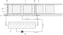
다결정 실리콘 태양 전지로부터 태양 전지를 제조하는 것은 공지된 것이고, 습식 화학 텍스쳐링 공정(wet-chemical texturing process)을 포함한다. 이 공정은 도 1에 도시한 바와 같이 일반적으로 연속 통과 플랜트(continuous passing-through plant)(인라인 에칭 플랜트(inline etching plant))에서 수행된다. 여기에서 수평으로 정렬된 웨이퍼(1)는 이송 롤(transport roll)(2) 상에서 플랜트를 통해 이송된다. 고정 롤(holding-down roll)(3)은 웨이퍼가 이송 롤과의 접촉을 상실하지 않도록 한다. 플랜트 내에는 웨이퍼가 분무 또는 침지 방식으로 화학 공정 용액에 노출되는 영역이 있다. 공정 용액(process solution)은 공정 용기(process basin)(4)에 존재할 수 있다. 넘친 매체(overflowing medium)는 파이프를 통해 탱크(5)로 다시 복귀하고, 이로부터 펌프(6)에 의해 공정 용기 안으로 다시 펌핑된다. 이 방법에서 공정 용액의 레벨은 첫 번째 및 마지막 쌍의 이송 및 고정 롤에 의해 이송 롤 영역에서 저류되어, 웨이퍼가 공정 용액에 완전히 침지된다. 이송 롤과 고정 롤 사이의 간격이 웨이퍼의 두께(보통 약 200㎛)에 해당하므로 이는 무시할 수 있다.Fabrication of solar cells from polycrystalline silicon solar cells is well known and involves a wet-chemical texturing process. This process is generally performed in a continuous passing-through plant (inline etching plant) as shown in FIG. 1 . Here the horizontally aligned
텍스처화를 위해, 불산(HF)과 질산(HNO3) 용액이 사용된다. 이 용액은 강한 발열 반응으로 실리콘과 반응하여 헥사플루오로규산(H2SiF6) 및 일산화질소(NO)를 형성하고, 이는 공기 중의 산소와 접촉하고 추가로 반응하여 이산화질소(NO2)를 형성한다.For texturing, hydrofluoric acid (HF) and nitric acid (HNO 3 ) solutions are used. This solution reacts with silicon in a strongly exothermic reaction to form hexafluorosilicic acid (H 2 SiF 6 ) and nitrogen monoxide (NO), which comes into contact with oxygen in the air and reacts further to form nitrogen dioxide (NO 2 ) .
이 방법에서 웨이퍼는 수평 정렬로 플랜트를 통해 안내되므로, 웨이퍼는 최대 면적을 필요로 하며, 이는 동시에 처리되는 웨이퍼의 수와 플랜트의 처리량을 제한한다. 따라서, 처리량의 증가는 처리 시간의 감소 또는 처리량 속도의 증가와 함께 플랜트의 증설에 의해서만 달성될 수 있다. 60초 내지 90초의 공정 시간은 이미 매우 짧기 때문에, 견고한 공정을 유지하면서 더 이상의 단축은 거의 불가능하다. 플랜트의 증설과 함께 처리량 속도의 증가는 경제적인 측면에서 크게 유리하지 않다. 이는 더 큰 플랜트 건설을 위한 필요한 자재 및 그에 따른 투자 비용도 증가하기 때문이다.In this method, the wafers are guided through the plant in horizontal alignment, so the wafers require a maximum area, which limits the number of wafers processed simultaneously and the throughput of the plant. Therefore, an increase in throughput can only be achieved by expanding the plant with a decrease in processing time or an increase in throughput rate. Since the process time of 60 seconds to 90 seconds is already very short, it is almost impossible to further shorten it while maintaining a robust process. The increase in throughput speed along with the expansion of the plant is not very advantageous from an economic point of view. This is because the materials required for the construction of larger plants and therefore the investment costs are also increased.
웨이퍼 처리는 기본적으로 인라인 방식(inline method)과 배치 방식(batch method)으로 구분할 수 있다. 인라인 방식에서 웨이퍼는 플랜트를 통해 차례로 열(row)로 이송된다. 여러 열의 웨이퍼를 동시에 나란히 이송할 수도 있다(다중 인라인 방식). 이에 반해, 배치 공정에서는 웨이퍼를 컨베이어 벨트 등에 놓고 개별적으로 이송되는 것이 아니라, 다수의 웨이퍼를 적재한 캐리어를 이용하여 이송된다.Wafer processing can be basically divided into an inline method and a batch method. In the inline method, wafers are transported in rows through the plant in turn. Multiple rows of wafers can be transferred side by side at the same time (multiple in-line method). On the other hand, in the batch process, the wafers are transferred using a carrier on which a plurality of wafers are loaded, rather than being individually transferred on a conveyor belt or the like.
DE 10 2006 054 846 A1은 인라인 플랜트 내의 웨이퍼가 배치로 플랜트를 통해 이송되기 위한 이송 배치 장치로 도입되는 장치를 제안한다. 그 후, 서로의 위에 적재된 여러 배치는 플랜트를 통해 안내되고, 플랜트의 끝에서 다시 단일화되어, 배치 모드의 이송은 이송 중 웨이퍼가 수직으로 정렬되도록 수행될 수도 있다. 그러나, 인라인 방식과 배치 방식을 결합하기 위해서는 기계적으로나 물류적으로나 정교한 조합과 단일화가 필요하다. 인라인 방식에서는 수직으로 정렬된 웨이퍼의 이송은 고려하지 않는다.DE 10 2006 054 846 A1 proposes a device in which wafers in an inline plant are introduced into a transfer batching device for transporting them through the batch to batch plant. Thereafter, several batches stacked on top of each other are guided through the plant and united again at the end of the plant, so that batch mode transfer may be performed such that the wafers are vertically aligned during transfer. However, in order to combine the inline method and the batch method, sophisticated combination and unification are required both mechanically and logistically. In the inline method, the transfer of vertically aligned wafers is not considered.
따라서, 이에 비추어, 본 발명의 목적은 종래 기술의 단점을 극복하는 웨이퍼의 처리 장치 및 방법을 제공하고자 한다. 특히, 증가된 처리량이 가능해야 한다. 또한, 배기 공기의 간소화된 후처리와 공정 용액의 구성요소의 소비 감소가 달성되어야 한다.Accordingly, in light of this, it is an object of the present invention to provide an apparatus and method for processing wafers that overcome the disadvantages of the prior art. In particular, increased throughput should be possible. In addition, a simplified after-treatment of the exhaust air and a reduction in the consumption of components of the process solution should be achieved.
상기 목적은 특허 청구항의 주제에 의해 달성된다. 상기 목적은 특히 화학 공정 용액으로 웨이퍼를 처리하기 위한 장치에 의해 달성되며, 상기 장치는 이송 수단(means of transport)(2) 및 고정 수단(holding-down means)(3) 뿐만 아니라 화학 공정 용액(process solution)을 수용하기 위한 적어도 하나의 공정 용기(process basin)(4)를 포함하고, 공정 용기(4)는 적어도 일 면 상에서 저류 장치(impounding device)(21)에 의해 제한되고, 저류 장치(21)는 이송 수단(2)과 고정 수단(3) 사이에서 수직으로 정렬된 웨이퍼가 수평 이동 방향으로 공정 용기(4) 안으로 안내되고 공정 용기(4) 밖으로 안내될 수 있다. 실시예에 따른 본 발명의 장치가 도 2 및 도 5에 도시된다.Said object is achieved by the subject matter of the patent claims. This object is achieved in particular by a device for treating wafers with a chemical process solution, said device comprising means of transport (2) and holding-down means (3) as well as chemical process solutions ( at least one
본 명세서에서 "수직" 및 "수평"이라는 용어가 사용되는 경우, 이는 달리 명시되지 않는 한 각각 "실질적으로 수직" 및 "실질적으로 수평"을 의미한다. 바람직하게는 기준점으로서 공정 용기(4)에 존재하는 공정 용액의 표면이 사용될 수 있다. 공정 용액의 파동(undulation)이나 다른 움직임이 없는 경우, 이 표면이 수평으로 정렬된다. 따라서, 공정 용액의 표면에 대해 수직인 표면 벡터가 수직이다. 따라서, "실질적으로 수평"이라는 문구는 바람직하게는 공정 용기(4)에 존재하는 공정 용액의 표면에 실질적으로 평행한 방향 또는 이동을 설명하는 반면, "실질적으로 수직"이라는 문구는 공정 용기(4)에 존재하는 공정 용액의 표면에 실질적으로 직교한 방향 또는 이동을 설명한다.Where the terms "vertical" and "horizontal" are used herein, they mean "substantially vertical" and "substantially horizontal" respectively, unless otherwise specified. Preferably, as a reference point, the surface of the process solution present in the
바람직하게는, 실질적으로 수평으로 배향된 표면에 대해 수직인 표면 벡터는 공정 용액의 표면에 대해 수직인 표면 벡터와 최대 20°, 더욱 바람직하게는 최대 10°, 더욱 바람직하게는 최대 5°, 더욱 바람직하게는 최대 1°, 더욱 바람직하게는 약 0°의 각도를 형성한다. 바람직하게는, 실질적으로 수평인 이동 방향의 벡터는 공정 용액의 표면에 대해 수직인 표면 벡터와 적어도 70° 및 최대 110°, 더욱 바람직하게는 적어도 80°및 최대 100°, 더욱 바람직하게는 적어도 85° 및 최대 95°, 더욱 바람직하게는 약 90°의 각도를 형성한다.Preferably, the surface vector perpendicular to the substantially horizontally oriented surface is at most 20°, more preferably at most 10°, even more preferably at most 5°, further with the surface vector perpendicular to the surface of the process solution. Preferably it forms an angle of at most 1°, more preferably about 0°. Preferably, the substantially horizontal vector in the direction of movement is at least 70° and at most 110°, more preferably at least 80° and at most 100°, even more preferably at least 85° with the surface vector perpendicular to the surface of the process solution. ° and up to 95°, more preferably about 90°.
바람직하게는, 실질적으로 수직으로 배향된 표면에 대해 수직인 표면 벡터는 공정 용액의 표면에 대해 수직인 표면 벡터와 적어도 70° 및 최대 110°, 더욱 바람직하게는 적어도 80° 및 최대 100°, 더욱 바람직하게는 적어도 85° 및 최대 95°, 더욱 바람직하게는 약 90°의 각도를 형성한다. 바람직하게는, 실질적으로 수직인 이동 방향의 벡터는 공정 용액의 표면에 대해 수직인 표면 벡터와 최대 20°, 더욱 바람직하게는 최대 10°, 더욱 바람직하게는 최대 5°, 더욱 바람직하게는 최대 1°, 더욱 바람직하게는 약 0°의 각도를 형성한다.Preferably, the surface vector perpendicular to the substantially vertically oriented surface is at least 70° and at most 110°, more preferably at least 80° and at most 100°, more preferably at least 70° and at most 110° with the surface vector perpendicular to the surface of the process solution Preferably it forms an angle of at least 85° and at most 95°, more preferably about 90°. Preferably, the vector in the direction of movement substantially perpendicular to the surface vector perpendicular to the surface of the process solution is at most 20°, more preferably at most 10°, still more preferably at most 5°, even more preferably at most 1 °, more preferably about 0 °.
본 발명의 장치는 화학 공정 용액으로 웨이퍼를 처리하기 위한 장치이다. 바람직하게는, 본 발명에 따른 장치를 이용하여 실리콘 웨이퍼, 특히 다결정 또는 단결정 실리콘 웨이퍼는 텍스처링 공정을 거쳐야 한다. 따라서, 바람직하게는 웨이퍼의 처리는 텍스처화이다. 이러한 웨이퍼의 텍스처화는 공지된 것이며, 주로 태양 전지의 생산에 사용된다. 바람직하게는, 다결정 웨이퍼에 사용되는 공정 용액은 불산(HF)과 질산(HNO3)을 포함하고, 단결정 웨이퍼에 사용되는 공정 용액은 수산화칼륨 수용액(KOH)과 하나 이상의 유기 첨가제의 혼합물을 포함한다.The apparatus of the present invention is an apparatus for processing wafers with chemical processing solutions. Preferably, a silicon wafer, in particular a polycrystalline or monocrystalline silicon wafer, is subjected to a texturing process using the apparatus according to the invention. Accordingly, preferably the processing of the wafer is texturing. The texturing of such wafers is known and is mainly used in the production of solar cells. Preferably, the process solution used for polycrystalline wafers comprises hydrofluoric acid (HF) and nitric acid (HNO 3 ), and the process solution used for single crystal wafers comprises a mixture of aqueous potassium hydroxide (KOH) and one or more organic additives. .
본 발명의 장치는 화학 공정 용액을 수용하기 위한 공정 용기(4)를 포함한다. 상기 장치는 또한 여러 공정 용기(4)를 포함하여, 예를 들어 여러 웨이퍼의 병렬 처리 또는 하나의 웨이퍼를 다른 공정 용액으로 순차적으로 처리할 수 있다. 동일한 처리 용기(4)에서 여러 웨이퍼를 동시에 및/또는 차례로 처리할 수 있다.The apparatus of the present invention comprises a process vessel (4) for containing a chemical process solution. The apparatus also comprises
본 발명의 바람직한 실시예에 따르면, 직사각형 베이스 영역을 갖는 공정 용기(4)가 사용된다. 공정 용기(4)의 폭은 병렬 방식으로 처리해야 하는 웨이퍼의 수 뿐만 아니라 두께 및 서로의 거리에 따라 주로 달라진다. 바람직하게는, 공정 용기(4)의 폭은 100mm 내지 1000mm, 더욱 바람직하게는 200mm 내지 800mm, 더욱 바람직하게는 500mm 내지 700mm의 범위이다. 공정 용기(4)의 길이는 웨이퍼가 공정 용기(4)에 있어야 하는 원하는 공정 시간에 따라 주로 달라지며, 공정 용기(4)를 통한 웨이퍼의 이송 속도가 고려되어야 한다. 바람직하게는, 공정 용기(4)의 길이는 100mm 내지 5000mm, 더욱 바람직하게는 300mm 내지 4000mm, 더욱 바람직하게는 800mm 내지 3000mm이다. 공정 용기(4)의 높이는 처리해야 하는 웨이퍼의 치수에 따라 주로 달라지므로 수직 정렬로 인해 웨이퍼의 길이와 폭에 따라 각각 달라진다. 바람직하게는, 공정 용기(4)는 공정 용기(4) 내의 웨이퍼가 공정 용액에 완전히 침지되도록 웨이퍼의 높이를 초과하는 높이로 공정 용액을 담을 수 있는 높이를 갖는다. 바람직하게는, 공정 용기(4)의 높이는 20mm 내지 2000mm, 더욱 바람직하게는 50mm 내지 1000mm, 더욱 바람직하게는 100mm 내지 500mm, 더욱 바람직하게는 150mm 내지 300mm, 더욱 바람직하게는 160mm 내지 250mm, 더욱 바람직하게는 180mm 내지 220mm의 범위이다.According to a preferred embodiment of the invention, a
본 발명의 장치는 이송 수단(2) 및 고정 수단(3)을 포함한다. 이송 수단(2)은 장치를 통한 웨이퍼 이송에 사용된다. 고정 수단(3)은 웨이퍼가 이송 수단(2)과의 접촉을 상실하지 않도록 한다. 이송 수단(2) 및 고정 수단(3)은 웨이퍼가 이송 수단(2)과 고정 수단(3) 사이에서 수직으로 정렬될 수 있고 상기장치를 통해 수평 이동 방향으로 안내될 수 있고, 특히 공정 용기(4) 안으로, 공정 용기(4)를 통해, 및 공정 용기(4) 밖으로 안내될 수 있도록 정렬된다.The device of the invention comprises a conveying means ( 2 ) and a fixing means ( 3 ). The transfer means 2 are used for transferring wafers through the apparatus. The fixing means 3 prevent the wafer from losing contact with the transfer means 2 . The conveying means 2 and the holding means 3 allow the wafers to be vertically aligned between the
이송 수단(2)과 고정 수단(3) 사이의 거리는 바람직하게는 실질적으로 웨이퍼의 길이 또는 폭에 해당하고, 종래 기술에서와 같이 웨이퍼의 두께에는 해당하지 않는다. 이송 수단(2)과 고정 수단(3) 사이의 거리는 이송 수단(2)과 고정 수단(3) 사이의 웨이퍼의 수직 정렬에 의해 결정된다. 특정 실시예에서, 이송 수단(2) 및/또는 고정 수단(3)은 수직 방향으로 이동 가능한 방식으로 정렬되어, 그들 사이의 거리가 유연한 방식으로 처리된 웨이퍼의 길이 또는 폭으로 조정될 수 있다. 일반적으로 웨이퍼의 길이는 웨이퍼의 폭에 해당한다. 따라서 일반적으로 웨이퍼는 정사각형의 기본 영역을 갖는다.The distance between the conveying
바람직하게는, 이송 수단(2)과 고정 수단(3) 사이의 간극은 10mm 내지 1000mm, 더욱 바람직하게는 20mm 내지 500mm, 더욱 바람직하게는 50mm 내지 300mm, 더욱 바람직하게는 100mm 내지 200mm, 더욱 바람직하게는 150mm 내지 170mm, 더욱 바람직하게는 약 156mm의 범위이다.Preferably, the gap between the conveying
바람직하게는, 상기 장치 내에서 이송 수단(2) 및 고정 수단(3)은 서로에 대해 실질적으로 평행하게 정렬된다. 이것이 또한 이송 수단(2)과 고정 수단(3) 사이의 웨이퍼의 수직 정렬에 유리하다.Preferably, in the device the conveying
이송 수단(2) 및/또는 고정 수단(3)은 예를 들어 컨베이어 벨트의 형태로 설계될 수 있다. 본 발명의 그러한 실시예가 가능하지만, 웨이퍼와 함께 이러한 컨베이어 벨트가 상기 장치를 통해, 특히 또한 공정 용기(4) 안으로, 공정 용기(4)를 통해. 및 공정 용기(4) 밖으로 안내되어야 하기 때문에 덜 유리하다. 따라서, 웨이퍼를 공정 용기(4) 안팎으로 안내하는 것 외에도, 컨베이어 벨트를 공정 용기(4) 안으로 안내하고 컨베이어 벨트를 공정 용기(4) 밖으로 안내하는데 문제가 있어서, 저류 장치(21)의 설계 가능성이 상당히 제한된다.The conveying means 2 and/or the fixing means 3 can be designed, for example, in the form of a conveyor belt. While such an embodiment of the present invention is possible, such a conveyor belt with wafers is carried through the apparatus, in particular also into the
따라서, 특히 바람직하게는, 이송 수단(2)은 이송 롤(2)이고, 고정 수단(3)은 고정 롤(3)이다. 롤 형태의 디자인은 이송 수단(2) 및 고정 수단(3) 자체가 공정 용기(4) 안으로, 공정 용기(4)를 통해 및 공정 용기(4) 밖으로 안내되어야 할 필요없이, 웨이퍼가 장치를 통해, 특히 공정 용기(4) 안으로, 공정 용기(4)를 통해 및 공정 용기(4) 밖으로 이송될 수 있다는 장점이 있다. 특히, 바람직하게는 이송 롤(2) 및 고정 롤(3)은 제자리에 고정된다. 따라서, 웨이퍼의 이송 동안, 바람직하게는 롤은 회전 운동만 실행하고, 병진 운동은 실행하지 않는다. 따라서, 바람직하게는, 롤은 상기 장치를 통해 웨이퍼와 함께 이동하지 않고 제자리에 유지된다. 이는 저류 장치(21)가 설계될 때 다양한 자유도를 제공하고, 이는 이송 수단(2) 및 고정 수단(3)이 공정 용기(4) 안으로, 공정 용기(4)를 통해 및 공정 용기(4) 밖으로 안내될 필요가 없기 때문에 이송 수단(2) 및 고정 수단(3)이 이송되는 것을 방지해야 하고, 웨이퍼를 공정 용기(4) 안으로, 공정 용기(4)를 통해 및 공정 용기(4) 밖으로 이송하기만 하면 되기 때문이다. 대신에, 바람직하게는 이송 롤러(2) 및 고정 롤러(3)는 공정 용기(4)의 내부 및 외부의 제자리에 각각 남아있도록 제공된다.Accordingly, particularly preferably, the conveying
바람직하게는, 이송 수단(2) 및/또는 고정 수단(3)은 웨이퍼를 고정하기 위한 적어도 하나의 리세스(recess), 바람직하게는 웨이퍼당 정확히 하나의 리세스를 포함한다. 이것은 옆으로 기울어지는 것(lateral tilting)으로부터 웨이퍼를 보호하는데 유리하다.Preferably, the conveying
이송 롤(2)과 고정 롤(3) 사이에 웨이퍼(1)가 위치하는 예시적인 실시예가 도 4에 도시된다.An exemplary embodiment is shown in FIG. 4 in which a
본 발명의 장치는 화학 공정 용액을 수용하기 위한 적어도 하나의 공정 용기(4)를 포함하며, 공정 용기(4)는 저류 장치(21)에 의해 적어도 일 면에서 제한된다. 화학 공정 용액으로 웨이퍼를 처리하는 것은 공정 용액이 내부에 존재하는 공정 용기(4)를 통해 웨이퍼를 안내함으로써 구현된다. 아래에서 자세히 설명하는 바와 같이, 저류 장치(21)는 이송 수단(2)과 고정 수단(3) 사이에서 수직으로 정렬된 웨이퍼가 공정 용기(4) 안으로 및 공정 용기(4) 밖으로 수평 이동 방향으로 안내될 수 있도록 설계된다. 따라서, 저류 장치(21)는 예를 들어 공정 용기(4)의 다른 경계 벽과 상이할 수 있으며, 저류 장치(21)가 개방 위치 및 폐쇄 위치를 취할 수 있으며, 개방 위치에서 수직으로 정렬된 웨이퍼가 공정 용기(4) 안으로 안내되거나 및/또는 수직으로 정렬된 웨이퍼가 공정 용기(4) 밖으로 안내되도록 저류 장치(21)는 이동 가능한 방식으로 배열된다. 예를 들어, 수직으로 정렬된 웨이퍼를 안내하기 위한 적어도 하나의 수직으로 진행하는 슬롯(22)을 갖는 저류 장치(21)를 제공할 수 있다. 저류 장치(21)가 이송 수단(2)과 고정 수단(3) 사이에서 수직으로 정렬된 웨이퍼가 공정 용기(4) 안으로 및 공정 용기(4) 밖으로 수평 이동 방향으로 안내될 수 있도록 설계되는 것이 보장되는 한, 나머지 설계에 관한 저류 장치(21)는 공정 수조(4)의 다른 경계 벽과 유사하게 설계될 수 있다.The apparatus of the present invention comprises at least one process vessel ( 4 ) for containing a chemical process solution, the process vessel ( 4 ) being confined on at least one side by a storage device ( 21 ). Treatment of wafers with a chemical process solution is implemented by guiding the wafer through a
저류 장치(21)는 슬롯(22)이 가능한 한 좁은 경우나 및/또는 저류 장치(21)가 가능한 한 두꺼운 경우 특히 효율적인 방식으로 작동하며, 이는 각각이 슬롯(22)의 유압 저항(hydraulic resistance)을 증가시키기 때문이다. The
바람직하게는, 저류 장치(21)의 두께는 웨이퍼 길이의 적어도 10%, 더욱 바람직하게는 웨이퍼 길이의 적어도 15%, 더욱 바람직하게는 웨이퍼 길이의 적어도 20%이고, 반면에 바람직하게는 웨이퍼 길이의 최대 50%, 더욱 바람직하게는 웨이퍼 길이의 최대 40%, 더욱 바람직하게는 웨이퍼 길이의 최대 30%이다. 바람직하게는, 저류 장치(21)의 두께는 15mm 내지 80mm, 더욱 바람직하게는 20mm 내지 60mm, 더욱 바람직하게는 30mm 내지 50mm의 범위이다.Preferably, the thickness of the
슬롯(22)의 폭은 바람직하게는 웨이퍼 두께의 최대 5배, 더욱 바람직하게는 최대 3배이고, 반면에 바람직하게는 웨이퍼 두께의 적어도 1.1배, 더욱 바람직하게는 적어도 1.5배이다. 바람직하게는, 슬롯(22)의 폭은 220㎛ 내지 1000㎛, 더욱 바람직하게는 300㎛ 내지 600㎛의 범위이다.The width of the
바람직하게는, 슬롯(22)은 입구 측에서 모따기(chamfer)되며, 즉 전면 섹션과 슬롯(22) 사이의 가장자리에는 바람직하게 모따기가 제공된다. 이것은 이송 시스템의 허용 오차인 경우에도 웨이퍼가 여전히 특히 신뢰할 수 있는 방식으로 삽입될 수 있도록 허용한다.Preferably, the
바람직하게는, 슬롯(22)의 폭은 공정 흐름 방향으로 가늘어진다. 이것이 슬롯(22)을 통한 웨이퍼의 보다 나은 안내에 기여한다. 이러한 실시예에서, 상술한 슬롯(22)의 폭은 가장 좁은 지점에서의 슬롯(22)의 폭을 의미한다. 가늘어진 슬롯의 폭인 경우, 가장 넓은 지점의 슬롯 폭 대비 가장 좁은 지점의 슬롯 폭의 비는 바람직하게는 1.1:1 내지 2:1, 더욱 바람직하게는 1.2:1 내지 1.5:1의 범위이다.Preferably, the width of the
특정 바람직한 실시예에서, 저류 장치(21) 앞의 고정 수단(3)은 유출되는 액체에 대해 특히 우수한 안내를 보장하기 위해 추가 중량을 갖도록 설계된다.In a particular preferred embodiment, the fastening means 3 in front of the
본 발명의 장치는 이송 수단(2)과 고정 수단(3) 사이의 웨이퍼 정렬과 상기 장치를 통한 웨이퍼의 보장된 이송으로부터 이미 알 수 있는 바와 같이 인라인 방법을 수행하는 데 적합하다. 인라인 방식에서 웨이퍼는 플랜트를 통해 개별적으로 하나씩 열로 이송된다. 여러 열의 웨이퍼를 동시에 나란히 운송할 수도 있다(다중 레인 인라인 방식).The device of the invention is suitable for carrying out the inline method, as can already be seen from the wafer alignment between the transport means 2 and the holding means 3 and the guaranteed transport of the wafers through the device. In inline, the wafers are transported individually as rows through the plant. Multiple rows of wafers can be transported side by side at the same time (multi-lane in-line).
종래 기술에서는 문제 없이 공정 용기(4)가 이송 롤(2)과 고정 롤(3)에 의해 제한될 수 있는데, 그 이유는 이송 롤(2)과 고정 롤(3) 사이의 거리가 웨이퍼의 두께에 실질적으로 해당되도록 웨이퍼가 수평 정렬로 이송되기 때문이다. 웨이퍼의 두께가 매우 얇기 때문에(보통 약 200㎛), 이송 롤(2)과 고정 롤(3) 사이의 간격으로 인해 공정 용기(4)로부터 공정 액체가 상당한 정도로는 유출되지 않는다.In the prior art, the
이와 대조적으로, 본 장치는 수직으로 정렬된 웨이퍼를 공정 용기(4) 안으로, 공정 용기(4)를 통해 및 공정 용기(4) 밖으로 인라인 이송하는 것을 포함한다. 웨이퍼의 수직 정렬로 인해, 이송 수단(2)과 고정 수단(3)의 거리는 종래 기술에서와 같이 웨이퍼의 두께에 해당하지 않고, 웨이퍼의 길이 또는 폭에 해당하고, 웨이퍼의 통상적인 정사각형 베이스 영역으로 인해 웨이퍼의 길이 및 폭은 일반적으로 동일하다. 웨이퍼의 길이와 폭은 두께의 여러 배수, 일반적으로 적어도 100배를 초과한다. 따라서 이송 수단(2)과 고정 수단(3) 사이의 거리가 너무 커서, 공정 용기(4)가 이송 수단(2)과 고정 수단에 의해 제한될 수 없으며, 이는 공정 용액이 이송 수단(2)과 고정 수단(3) 사이의 공간을 통해 누출되어, 공정 용액이 웨이퍼를 처리하기에 충분한 양으로 공정 용기(4) 내에 남아있지 않기 때문이다.In contrast, the apparatus involves inline transfer of vertically aligned wafers into, through, and out of
공정 용기(4)를 공통 경계벽으로 모든 면에서 제한하는 것은 인라인 방법을 수행하는 데 적합해야 하는 장치에서 만족스러운 솔루션일 수 없다. 이는 수직으로 정렬된 웨이퍼가 공정 용기(4) 안으로 및 공정 용기(4) 밖으로 수평 이동 방향으로 안내할 수 있는 것을 방지하기 때문이다. 오히려 웨이퍼를 수직으로 들어올려 경계벽 위로 안내한 다음 공정 용기(4) 안으로 웨이퍼를 수직으로 내려야하며, 이는 인라인 방법과 호환되지 않는다.Confining the
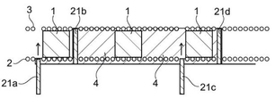
따라서, 본 발명의 장치의 공정 용기(4)는 이송 수단(2)과 고정 수단(3) 사이에서 수직으로 정렬된 웨이퍼를 공정 용기(4) 안으로 및 공정 용기(4) 밖으로 수평 이동 방향으로 안내할 수 있도록 설계된 저류 장치(21)에 의해 적어도 일 면이 제한된다. 공정 용기(4)의 다른 면 중 하나 이상은 또한 이러한 저류 장치(21)에 의해 제한될 수 있다. 그러나 상기 장치로 인라인 방법을 수행하는 데 필요한 것은 아니다. 이러한 저류 장치(21)에 의해 공정 용기(4)가 적어도 일 면에서 제한되는 경우면 충분하다. 그러한 실시예에서, 웨이퍼는 그들이 또한 공정 용기(4) 안으로 안내된 동일일 면에서 공정 용기(4) 밖으로 안내된다. 공정 용기(4)의 남은 면은, 예를 들어 공정 용기(4)로부터 공정 용액의 누출을 피하기 위해 정상적인 경계벽의 형태로 설계될 수 있다.Thus, the
그러나, 공정 용기의 일 면에만 설명된 저류 장치(21)가 존재하는 실시예는 웨이퍼가 공정 용기(4)로 도입되는 동일 면에서 공정 용기(4)로부터 방출되기 때문에 공정 용기(4) 내에서 웨이퍼의 보다 복잡한 이송 안내를 필요로 한다. 따라서, 바람직하게는, 본 발명의 장치는 공정 용기(4)의 대향 면에 존재하는 2개의 저류 장치(21a, 21b)를 포함한다. 이것은 웨이퍼가 일 면에서 공정 용기(4)로 도입될 수 있고 다른 면에서 공정 용기(4)로부터 방출될 수 있기 때문에 공정 용기(4) 안으로, 공정 용기(4)를 통해 및 공정 용기(4) 밖으로 웨이퍼의 선형 이송을 허용한다. 그러한 실시예에서는 웨이퍼의 이동 방향을 변경할 필요가 없다.However, the embodiment in which the
저류 장치(21)의 재료는 각각의 용도, 특히 공정 온도 및/또는 화학적 에칭 용액의 성분에 따라 달라진다.The material of the
본 발명의 저류 장치(21)는 이송 수단(2)과 고정 수단(3) 사이에서 수직으로 정렬된 웨이퍼가 공정 용기(4) 안으로 및 공정 용기(4) 밖으로 수평 이동 방향으로 안내될 수 있도록 설계된다.The
특정 실시예에서, 저류 장치(21)는 저류 장치(21)가 개방 위치 및 폐쇄 위치를 취할 수 있고, 개방 위치는 수직으로 정렬된 웨이퍼를 공정 용기(4) 안으로 및/또는 공정 용기(4) 밖으로 안내할 수 있도록 이동 가능한 방식으로 배열된다. 예를 들어, 저류 장치(21)는 개방 위치로 아래쪽으로 낮춰지거나, 개방 위치로 들어올리거나 위쪽으로 당길 수 있도록 설계될 수 있어서, 수직으로 정렬된 웨이퍼를 공정 용기(4) 안으로 안내하거나 및/또는 수직으로 정렬된 웨이퍼를 공정 용기(4) 밖으로 안내한다.In a particular embodiment, the
본 발명의 그러한 설계는 가능하지만, 특정 단점을 수반한다. 저류 장치(21)가 폐쇄 위치가 아니라 개방 위치일 때, 화학 공정 용액은 이러한 경우에 공정 용기(4)로부터 상당한 정도로 누출될 것이기 때문이다. 따라서, 이와 같이 설계된 저류 장치(21)를 갖는 본 발명의 장치는 연속 작동에 사용될 수 없다. 오히려, 공정 용기(4) 안으로 웨이퍼를 로딩한 후 저류 장치(21)를 개방 위치에서 폐쇄 위치로 변경하여, 공정 용기(4) 안으로 도입된 공정 액체를 공정 용기(4)의 개구부를 통해 다시 누출되도록 해야 하고, 이는 저류 장치(21)가 개방 위치에 있다는 사실에서 기인한다. 이를 위해서는 플랜트를 통한 웨이퍼 운송을 중단해야 한다. 저류 장치(21)가 다시 폐쇄 위치에 있을 때만 공정 용액이 현재 폐쇄된 공정 용기(4)에 제공된다. 웨이퍼가 공정 용기(4) 밖으로 안내되도록 하기 위해, 저류 장치(21)를 다시 개방 위치로 가져와야 한다. 바람직하게는, 저류 장치(21)가 개방 위치일 때, 공정 용기(4)로부터 공정 액체의 제어되지 않은 누출을 방지하기 위해, 공정 액체 또는 이의 적어도 대부분이 공정 용기(4)로부터 다시 제거된다.Such a design of the present invention is possible, but carries certain disadvantages. This is because when the
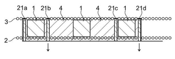
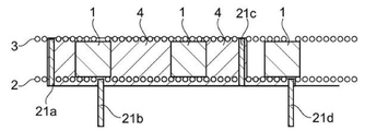
공정 용기(4)로부터 공정 액체의 과도한 누출을 방지하기 위해, 저류 장치(21)는 또한 2개의 위어(weir)(21a, 21b)를 통해 로딩 영역(loading region)이 형성되고 2개의 위어(21c, 21d)를 통해 언로딩 영역(unloading region)이 형성되도록 설계될 수 있다. 가능한 설계는 예를 들어 도 6에 도시된다. 여기에서, 위어(21a, 21b, 21c, 21d)는 각각 인입식(retractable) 위어로 도시된다. 대안으로, 위어를 개방 위치로 들어 올리거나 당기는 것도 가능하다. 2개의 위어가 각각 로딩 영역 및 언로딩 영역을 형성한다는 사실로 인해, 공정 용기(4)로부터의 공정 액체의 과도한 누출이 방지될 수 있다. 예를 들어, 내륙 수로 운송(inland waterway transport)의 잠금 장치에서도 유사한 원리가 알려져 있다.In order to prevent excessive leakage of the process liquid from the
이 작동 모드에서는 웨이퍼가 각각 그룹으로 공정 용기(4) 안팎으로 안내되기 때문에, 웨이퍼를 웨이퍼 그룹으로 나눌 필요가 있다. 일반적으로 두 개의 연속 웨이퍼 그룹 사이의 거리는 적어도 하나의 웨이퍼 길이가 되어, 공간 요구 사항이 증가할 것이다. 병렬 방식으로 여러 웨이퍼 그룹이 공정 용기(4) 안으로 안내되고 공정 용기(4) 밖으로 안내되는 다중 레인 인라인 방법에서는 또한 단일 웨이퍼들이 실제로 평행하다는 것이 보장되어야 하며, 이는 그렇지 않으면 저류 장치(21)가 개방 위치에서 폐쇄 위치로 변경될 때 저류 장치(21)와 일치하지 않는 웨이퍼의 원하지 않는 상호 작용이 발생할 수 있기 때문이며, 이는 각각의 웨이퍼 및/또는 저류 장치(21)의 손상을 초래할 수 있다.Since in this mode of operation the wafers are each guided into and out of the
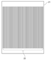
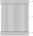
따라서, 상기 장치의 연속 작동을 허용하는 저류 장치(21)의 설계가 바람직하다. 바람직하게는, 저류 장치(21)에는 수직으로 정렬된 웨이퍼를 안내하기 위한 적어도 하나의 수직으로 진행하는 슬롯(22)이 제공된다. 단일 레인 인라인 방법에서는, 수직으로 정렬된 웨이퍼를 안내하기 위한 정확히 하나의 수직으로 진행하는 슬롯(22)이 저류 장치(21)에 제공되면 충분하다. 다중 레인 인라인 방법에서는 여러 열의 웨이퍼가 동시에 나란히 이송된다. 그러한 경우에, 저류 장치(21)에는 수직으로 정렬된 웨이퍼를 안내하기 위한 하나 이상의 수직으로 진행하는 슬롯(22)이 제공될 수 있다. 특히, 슬롯(22)의 수는 병렬 방식으로 처리되는 웨이퍼의 열의 수와 일치해야 한다. 바람직한 실시예에서, 저류 장치(21)에는 2개 내지 1000개, 더욱 바람직하게는 5개 내지 500개, 더욱 바람직하게는 10개 내지 200개, 더욱 바람직하게는 20개 내지 100개, 더욱 바람직하게는 30개 내지 50개의 수직으로 진행하는 슬롯(22)이 제공되어, 수직으로 정렬된 웨이퍼를 안내한다. 슬롯(22)을 갖는 저류 장치(21)의 예시적인 실시예가 도 3에 도시된다.Therefore, a design of the
슬롯(22)의 서로간의 거리는 병렬 방식으로 처리되는 웨이퍼 열의 거리에 따라 달라진다. 바람직하게는, 슬롯(22)의 서로간의 거리는 슬롯(22)의 폭의 2배 내지 100배, 더욱 바람직하게는 5배 내지 50배, 더욱 바람직하게는 10배 내지 30배, 더욱 바람직하게는 20배 내지 25배이다. 바람직하게는, 슬롯(22)의 서로간의 거리는 0.4mm 내지 40mm, 더욱 바람직하게는 1mm 내지 10mm, 더욱 바람직하게는 2mm 내지 6mm, 더욱 바람직하게는 4mm 내지 5mm, 더욱 바람직하게는 4.5mm 내지 4.9mm, 더욱 바람직하게는 4.7mm 내지 4.8mm이다. The distance of the
슬롯(22)은 다른 방식으로 저류 장치(21)에 도입될 수 있다. 바람직하게는, 슬롯(22)은 저류 장치(21) 내로 밀링된다. 다른 바람직한 실시예에서, 저류 장치(21)는 특히 적층 제조, 예를 들어 3D 프린팅에 의해 슬롯(22)과 함께 미리 제조된다.The
바람직하게는, 수직 정렬에 대한 정면도에서 슬롯(22)의 치수는 웨이퍼의 치수에 실질적으로 해당한다. 이것은 공정 용기(4)로부터 공정 용액의 바람직하지 않은 증가된 누출을 수반할 수 있는 불필요하게 큰 치수의 슬롯(22)에 대한 필요 없이, 슬롯(22)을 통해 수직으로 정렬된 웨이퍼를 수평 이동 방향으로 안내한다.Preferably, the dimensions of the
바람직하게는, 슬롯(22)은 10mm 내지 1000mm, 더욱 바람직하게는 20mm 내지 500mm, 더욱 바람직하게는 50mm 내지 300mm, 더욱 바람직하게는 100mm 내지 200mm, 더욱 바람직하게는 150mm 내지 170mm, 더욱 바람직하게는 156mm 내지 168mm, 더욱 바람직하게는 160mm 내지 165mm의 범위의 높이를 갖는다. 바람직하게는, 슬롯(22)의 높이는 이송 수단(2)과 고정 수단(3) 사이의 거리에 실질적으로 해당한다. Preferably, the
슬롯(22)의 폭은 바람직하게는 웨이퍼 두께의 최대 5배, 더욱 바람직하게는 최대 3배, 그러나 바람직하게는 웨이퍼 두께의 적어도 1.1배, 더욱 바람직하게는 적어도 1.5배이다. 슬롯(22)의 폭은 바람직하게는 220㎛ 내지 1000㎛, 더욱 바람직하게는 300㎛ 내지 600㎛이다.The width of the
슬롯(22)의 깊이는 저류 장치(21)의 깊이에 따라 달라진다. 바람직하게는, 슬롯(22)의 깊이는 웨이퍼 길이의 적어도 10%, 더욱 바람직하게는 웨이퍼 길이의 적어도 15%, 더욱 바람직하게는 웨이퍼 길이의 적어도 20%, 그러나 바람직하게는 웨이퍼 길이의 최대 50%, 더욱 바람직하게는 웨이퍼 길이의 최대 40%, 더욱 바람직하게는 웨이퍼 길이의 최대 30%이다. 바람직하게는, 슬롯(22)의 깊이는 15mm 내지 80mm, 더욱 바람직하게는 20mm 내지 60mm, 더욱 바람직하게는 30mm 내지 50mm 범위이다.The depth of the
따라서, 본 발명에 따른 장치를 사용하면 여러 열의 웨이퍼(1), 특히 2 내지 1000열의 웨이퍼(1), 예를 들어 5열 내지 500열의 웨이퍼(1), 10열 내지 200열의 웨이퍼(1), 20열 내지 100열의 웨이퍼(1), 또는 30열 내지 50열의 웨이퍼(1)가 동일한 공정 용기(4)를 통해 동시에 나란히 이송될 수 있다. 바람직하게는, 공정 용기(4)를 통해 나란히 동시에 이송되는 두 열의 웨이퍼(1)의 서로간의 거리는 0.4mm 내지 40mm, 더욱 바람직하게는 1mm 내지 10mm, 더욱 바람직하게는 2mm 내지 6mm, 더욱 바람직하게는 4mm 내지 5mm, 더욱 바람직하게는 4.5mm 내지 4.9mm, 더욱 바람직하게는 4.7mm 내지 4.8mm이다.Thus, using the device according to the invention, several rows of
바람직하게는, 상기 장치는 공정 용기(4)와 연결된 탱크(5)를 포함하여, 화학 공정 용액을 탱크(5)로부터 공정 용기(4)로 이송할 수 있다. 바람직하게는, 상기 장치는 펌프(6)를 포함하여 탱크(5)로부터 공정 용기(4)로 화학 공정 용액을 이송한다.Preferably, the apparatus comprises a
바람직하게는, 상기 장치는 적어도 하나의 수집 용기(collecting basin)를 포함하여, 공정 용기(4)로부터 누출되는 공정 용액을 수용한다. 바람직하게는, 수집 용기는 탱크(5)와 연결되어 수집 용기에 수용된 공정 용액이 탱크(5)로 복귀될 수 있다. 따라서, 공정 용기(4)에서 누출된 공정 용액을 손실하지 않고 웨이퍼 처리에 다시 사용할 수 있다.Preferably, the apparatus comprises at least one collecting basin to receive the process solution leaking from the process vessel (4). Preferably, the collection vessel is connected to the
본 발명은 또한 하기 단계를 포함하는 화학 공정 용액으로 웨이퍼를 처리하는 인라인 방법에 관한 것이다:The present invention also relates to an inline method for treating a wafer with a chemical process solution comprising the steps of:
a) 수직으로 정렬된 웨이퍼를 제공하는 단계,a) providing a vertically aligned wafer;
b) 내부에 공정 용액이 존재하는 공정 용기(4)를 제공하는 단계,b) providing a process vessel (4) having a process solution therein;
c) 수직으로 정렬된 웨이퍼를 공정 용기(4) 안으로 안내하는 단계,c) guiding the vertically aligned wafer into the process vessel (4);
d) 웨이퍼가 공정 용액에 접촉되도록, 수직으로 정렬된 웨이퍼를 내부에 공정 용액이 존재하는 공정 용기(4)를 통해 안내하는 단계;d) guiding the vertically aligned wafer through the
e) 수직으로 정렬된 웨이퍼를 공정 용기(4) 밖으로 안내하는 단계를 포함하며,e) guiding the vertically aligned wafer out of the process vessel (4);
c) 내지 e) 단계에 따른 단계에서의 안으로 안내, 통해 안내 및 밖으로 안내하는 것은 실질적으로 수평 이동 방향으로 수행된다. 바람직하게는 상기 방법은 본 발명의 장치로 수행된다.Guiding in, guiding through and guiding out in the steps according to steps c) to e) are performed in a substantially horizontal direction of movement. Preferably the method is carried out with the apparatus of the present invention.
본 발명의 방법은 인라인 방법이다. 인라인 방법에서는 웨이퍼가 플랜트를 통해 차례로 열로 이송된다. 여러 열의 웨이퍼를 동시에 나란히 운송하는 것도 가능하다(다중 인라인 방식).The method of the present invention is an inline method. In the in-line method, wafers are thermally transported one after another through the plant. It is also possible to transport several rows of wafers side-by-side at the same time (multiple in-line).
바람직하게는, 여러 열의 웨이퍼(1), 특히 2열 내지 1000열의 웨이퍼(1), 예를 들어 5열 내지 500열의 웨이퍼(1), 10열 내지 200열의 웨이퍼(1), 20열 내지 100열의 웨이퍼(1) 또는 30열 내지 50열의 웨이퍼(1)가 동일한 공정 용기(4)를 통해 동시에 나란히 이송된다. 바람직하게는, 공정 용기(4)를 통해 동시에 나란히 이송되는 두 열의 웨이퍼(1)의 서로간의 거리는 0.4mm 내지 40mm, 더욱 바람직하게는 1mm 내지 10mm, 더욱 바람직하게는 2mm 내지 6mm, 더욱 바람직하게는 4mm 내지 5mm, 더욱 바람직하게는 4.5mm 내지 4.9mm, 더욱 바람직하게는 4.7mm 내지 4.8mm이다.Preferably, several rows of
본 발명의 방법은 화학 공정 용액으로 웨이퍼를 처리하는 방법이다. 바람직한 웨이퍼는 실리콘 웨이퍼, 특히 다결정질 실리콘 웨이퍼이다. 웨이퍼의 처리는 바람직하게는 텍스처화이다. 이러한 웨이퍼의 텍스처화는 공지된 것이며 주로 태양 전지의 제조에 사용된다. 바람직하게는, 사용되는 공정 용액은 불산(HF) 및 질산(HNO3)을 포함한다.The method of the present invention is a method of treating a wafer with a chemical processing solution. Preferred wafers are silicon wafers, in particular polycrystalline silicon wafers. The processing of the wafer is preferably texturing. The texturing of such wafers is known and is mainly used in the manufacture of solar cells. Preferably, the process solution used comprises hydrofluoric acid (HF) and nitric acid (HNO 3 ).
본 발명에 따른 방법의 a) 단계에 따르면, 수직으로 정렬된 웨이퍼가 제공된다. 웨이퍼의 길이와 폭은 두께보다 몇 배, 일반적으로 100배 내지 1000배를 초과한다. 이로부터 웨이퍼는 웨이퍼의 길이와 폭으로 각각 정의되는 두 개의 주요 표면을 갖는다. 또한, 원형의 주요 표면을 갖는 웨이퍼가 고려될 수 있으며, 여기서 주요 표면은 둘레에 의해 제한된다. 웨이퍼의 실질적인 수직 정렬은 주요 표면에 대해 수직인 표면 벡터가 실질적으로 수평으로 배향되도록 배열되도록 웨이퍼의 두 주요 표면이 정렬되는 방향을 의미한다. 바람직하게는, 두 주요 표면의 표면 벡터는 상기 방법의 c) 내지 e) 단계의 이동에 따른 웨이퍼의 수평 이동 방향의 벡터와 적어도 70° 및 최대 110°, 더욱 바람직하게는 적어도 80° 및 최대 100°, 더욱 바람직하게는 적어도 85° 및 최대 95°, 더욱 바람직하게는 약 90°의 각도를 형성한다.According to step a) of the method according to the invention, a vertically aligned wafer is provided. The length and width of the wafer are several times greater than the thickness, typically 100 to 1000 times greater. From this the wafer has two major surfaces, each defined by the length and width of the wafer. Also contemplated are wafers having a circular major surface, wherein the major surface is bounded by the perimeter. Substantially vertical alignment of the wafer refers to the direction in which the two major surfaces of the wafer are aligned such that a surface vector perpendicular to the major surface is oriented substantially horizontally. Preferably, the surface vectors of the two major surfaces are at least 70° and at most 110°, more preferably at least 80° and at most 100 with the vector in the direction of horizontal movement of the wafer according to the movement of steps c) to e) of the method. °, more preferably at least 85° and at most 95°, more preferably about 90°.
본 발명에 따른 방법의 b) 단계에 따르면, 내부에 공정 용액이 존재하는 공정 용기(4)가 제공된다. 바람직하게는, 공정 용액은 다결정 웨이퍼의 텍스처화의 경우 불산(HF)과 질산(HNO3)을 포함하거나 단결정 웨이퍼의 텍스처화의 경우 수산화칼륨 용액(KOH)과 하나 이상의 유기 첨가제의 혼합물을 포함한다.According to step b) of the method according to the invention, a process vessel ( 4 ) with a process solution present therein is provided. Preferably, the process solution comprises hydrofluoric acid (HF) and nitric acid (HNO 3 ) for texturing polycrystalline wafers or a mixture of potassium hydroxide solution (KOH) and one or more organic additives for texturing single crystal wafers. .
화학 공정 용액에 의한 웨이퍼의 처리는 웨이퍼를 공정 용기(4)를 통해 안내하여, 웨이퍼가 공정 용기(4)에 존재하는 공정 용액과 접촉됨으로써 수행된다. 웨이퍼를 공정 용기(4) 안으로 안내하고 웨이퍼를 공정 용기(4) 밖으로 안내하는 사이의 시간은 다결정질 웨이퍼의 경우 바람직하게는 15초 내지 180초, 더욱 바람직하게는 30초 내지 120초, 더욱 바람직하게는 60초 내지 90초이고, 단결정 웨이퍼의 경우 바람직하게는 0.5분 내지 15분, 더욱 바람직하게는 1분 내지 10분, 더욱 바람직하게는 2분 내지 6분이다.The processing of the wafer by the chemical process solution is performed by guiding the wafer through the
본 발명에 따른 방법의 c) 내지 e) 단계에 따른 (수직으로 정렬된 웨이퍼의) 안으로 안내, 통해 안내 및 밖으로 안내하는 것은 실질적으로 수평 이동 방향으로 수행된다. 이는 c) 내지 e) 단계 동안 공정 용액의 표면으로부터 단일 웨이퍼의 무게 중심과의 거리가 실질적으로 변하지 않도록 웨이퍼를 안내하는 것을 의미한다. 바람직하게는, c) 내지 e) 단계 동안 공정 용액의 표면으로부터 단일 웨이퍼의 무게 중심의 최대 거리와 최소 거리 사이의 차이는 각각의 웨이퍼의 길이의 최대 20%, 더욱 바람직하게는 최대 10%이고, 더욱 바람직하게는 최대 5%, 더욱 바람직하게는 최대 2%, 더욱 바람직하게는 최대 1%이다.The guiding in, guiding through and out guiding (of the vertically aligned wafer) according to steps c) to e) of the method according to the invention is carried out in a substantially horizontal direction of movement. This means guiding the wafer so that the distance from the surface of the process solution to the center of gravity of the single wafer during steps c) to e) does not change substantially. Preferably, the difference between the maximum distance and the minimum distance of the center of gravity of a single wafer from the surface of the process solution during steps c) to e) is at most 20%, more preferably at most 10% of the length of each wafer, More preferably at most 5%, more preferably at most 2%, even more preferably at most 1%.
상기 방법의 c) 내지 e) 단계 동안 웨이퍼의 이동 속도는 바람직하게는 0.5m/min 내지 10m/min, 더욱 바람직하게는 1m/min 내지 6m/min의 범위이다.The moving speed of the wafer during steps c) to e) of the method is preferably in the range from 0.5 m/min to 10 m/min, more preferably from 1 m/min to 6 m/min.
본 발명은 또한 태양 전지 및/또는 인쇄 기판의 제조를 위한 본 발명의 장치 및/또는 방법의 용도에 관한 것이다.The invention also relates to the use of the device and/or method of the invention for the manufacture of solar cells and/or printed boards.
도 1은 종래 기술의 장치에 의한 단면도를 도시한다. 웨이퍼(1)는 상기 장치를 통해 수평 정렬로 이송된다. 공정 용기(4)는 이송 롤(2)과 고정 롤(3)에 의해 제한된다. 넘친 매체는 파이프를 통해 탱크(5)로 복귀하고, 펌프(6)를 통해 다시 공정 용기(4)로 펌핑된다. 화살표는 매체의 흐름 방향을 나타낸다.
도 2는 본 발명의 장치에 의한 단면도를 도시한다. 웨이퍼(1)는 상기 장치를 통해 수직 정렬로 이송된다. 상기 장치는 화학 공정 용액을 수용하기 위한 공정 용기(4)를 포함한다. 공정 용기(4)는 저류 장치(21)에 의해 두 면이 제한된다. 넘친 매체는 파이프를 통해 탱크(5)로 복귀하고 펌프(6)를 통해 다시 공정 용기(4)로 펌핑된다. 화살표는 매체의 흐름 방향을 나타낸다. 화학 공정 용액으로 웨이퍼(1)를 처리하는 것은 공정 용액이 내부에 존재하는 공정 용기(4)를 통해 웨이퍼(1)를 안내함으로써 달성된다. 저류 장치(21)는 이송 수단(2)과 고정 수단(3) 사이에서 수직으로 정렬된 웨이퍼(1)가 수평 이동 방향으로 공정 용기(4) 안으로 안내될 수 있고 공정 용기(4) 밖으로 안내될 수 있도록 설계된다.
도 3은 수직 정렬로 이송되는 웨이퍼를 위한 통로로서 슬롯(22)을 갖는 저류 장치(21)의 정면도를 도시한다.
도 4는 사이에 수직으로 정렬된 웨이퍼(1)가 포함된 이송 롤(2)과 고정 롤(3)의 정면도를 도시한다.
도 5는 본 발명의 장치의 사시도를 도시한다. 저류 장치(21)는 이송 수단(2)과 고정 수단 사이에서 수직으로 정렬된 웨이퍼(1)가 수평 이동 방향으로 공정 용기(4) 안으로 안내될 수 있고 공정 용기(4) 밖으로 안내될 수 있도록 설계된다. 명확성을 위해 고정 수단은 도시하지 않는다.
도 6은 수직 정렬로 상기 장치를 통해 이송되는 웨이퍼(1)를 갖는 본 발명의 장치에 의한 단면도를 도시한다. 저류 장치(21)는 이송 수단(2)과 고정 수단(3) 사이에서 수직으로 정렬된 웨이퍼(1)가 수평 이동 방향으로 공정 용기(4) 안으로 안내될 수 있고 공정 용기(4) 밖으로 안내될 수 있도록 설계된다. 두 개의 위어(21a, 21b)를 통해 로딩 영역이 형성되고 두 개의 위어(21c, 21d)를 통해 언로딩 영역이 형성되도록 저류 장치(21)가 설계된 실시예가 도시된다. 위어(21a, 21b, 21c, 21d)는 각각 인입식 위어이다. 로딩 및 언로딩을 위해, 먼저 위어(21a, 21c)가 낮아져 웨이퍼가 로딩 및 언로딩 영역으로 이동될 수 있다(도 6a). 이어서, 위어(21a, 21c)가 폐쇄 위치로 이동되어, 도 6b에 도시된 배열이 생성된다. 위어(21b, 21d)를 개방 위치로 이동시킨 후, 로딩될 웨이퍼(1)는 공정 영역으로 이송되는 반면, 언로딩될 웨이퍼( )는 언로딩 영역을 떠난다(도 6c 및 6d). 로딩 및 언로딩 영역이 다시 비점유되면, 위어(21b, 21d)는 폐쇄 위치로 이동되고, 위어(21a, 21b)는 개방 위치로 이동되어, 다음 웨이퍼(1) 각각이 로딩 및 언로딩으로 이동될 수 있고, 다시 도 6a에 도시된 배열이 생성된다.1 shows a cross-sectional view by means of a prior art device; The
2 shows a cross-sectional view by means of the device of the present invention. The
3 shows a front view of a
4 shows a front view of a
5 shows a perspective view of the device of the present invention; The
Figure 6 shows a cross-sectional view by means of an apparatus of the invention with a
공정 플랜트를 통한 수직으로 정렬된 웨이퍼의 이송Transfer of vertically aligned wafers through the process plant
이송을 위해 웨이퍼는 에지 방향 및 표면-평행 방식으로 공정 플랜트를 통해 이동된다. 따라서 웨이퍼 당 필요한 공간은 약 160x160㎟에서 160x5㎟로 감소하여 병렬 방식으로 처리되는 웨이퍼가 상당히 증가하여 플랜트의 처리량이 상당히 증가한다.For transport, wafers are moved through the process plant in an edge-wise and surface-parallel manner. Thus, the space required per wafer is reduced from about 160x160mm2 to 160x5mm2, which significantly increases the number of wafers processed in parallel, significantly increasing the throughput of the plant.
이송 중 웨이퍼의 수평 정렬이 예상되는 선행 기술과 달리, 본 방법에서는 이송 롤 및 고정 롤만으로는 공정 용액을 저류하는 것이 더 이상 가능하지 않으며, 이는 이제 두 롤 사이의 거리가 웨이퍼의 가장자리 길이(156mm)에 해당하기 때문이다. 따라서 저류 장치(21)의 추가 설치가 필요하다. 이 저류 장치(21)에는 웨이퍼가 저류된 공정 용액 내로 이동될 수 있는 다수의 슬롯(22)(이는 웨이퍼의 수에 해당함)이 제공된다. 이 경우, 50개의 웨이퍼가 병렬 처리되며, 저류 장치(21)에는 50개의 슬롯(22)이 제공된다.Contrary to the prior art, where horizontal alignment of the wafer during transfer is expected, in this method it is no longer possible to store the process solution with only the transfer roll and the stationary roll, which means that the distance between the two rolls is now the edge length of the wafer (156 mm). because it corresponds to Therefore, additional installation of the
가능한 한 정확한 웨이퍼의 수직 정렬을 달성하기 위해 이송 롤(2)과 고정 롤(3)에는 프로파일(profile)이 제공되어 웨이퍼가 롤의 작은 홈으로 안내되고 측면 기울임이 방지된다.In order to achieve the vertical alignment of the wafers as accurate as possible, the
웨이퍼를 수직으로 최대한 정확하게 정렬하기 위해, 이송 롤러(2)와 고정 롤러(3)에는 웨이퍼가 롤의 작은 리세스로 안내되고 측방향 기울임이 방지되도록 프로파일이 제공된다.In order to align the wafers vertically as accurately as possible, the
수직 정렬로 웨이퍼를 이송하여 처리량을 크게 증가시킬 수 있다.Transferring wafers in vertical alignment can significantly increase throughput.
더 많은 처리량 외에도, 동시에 처리되는 웨이퍼의 수에 비해 수조(bath) 표면이 실질적으로 더 작다. 따라서, 질소 산화물은 보다 농축된 형태로 배기 공기로 방출되어, 후처리가 단순화된다.In addition to higher throughput, the bath surface is substantially smaller compared to the number of wafers being processed simultaneously. Thus, nitrogen oxides are released into the exhaust air in a more concentrated form, simplifying the after-treatment.
또한, 더 작은 수조 표면에 의해 배기 공기의 질소 산화물의 총 부하가 감소된다. 질소 산화물의 일부가 공정 용액에 남아 있고, 그곳에서 추가로 반응한다. 따라서, 에칭 공정에서 질산의 소비가 감소된다.In addition, the total load of nitrogen oxides in the exhaust air is reduced by the smaller bath surface. Some of the nitrogen oxides remain in the process solution, where they react further. Accordingly, the consumption of nitric acid in the etching process is reduced.
Claims (15)
상기 장치는 이송 수단(2) 및 고정 수단(3) 뿐만 아니라 화학 공정 용액을 수용하기 위한 적어도 하나의 공정 용기(4)를 포함하며, 공정 용기(4)는 적어도 일 면 상에서 저류 장치(21)에 의해 제한되고, 저류 장치(21)는 이송 수단(2)과 고정 수단(3) 사이에서 수직으로 정렬된 웨이퍼가 수평 이동 방향으로 공정 용기(4) 안으로 안내되고, 공정 용기(4) 밖으로 안내되도록 설계된 장치.An apparatus for processing a wafer with a chemical process solution, comprising:
The apparatus comprises at least one process vessel (4) for receiving chemical process solutions as well as transport means (2) and fixing means (3), the process vessel (4) having a storage device (21) on at least one side and the storage device 21 guides the wafers vertically aligned between the transfer means 2 and the fixing means 3 into the process container 4 in the horizontal movement direction and out of the process container 4 . devices designed to be.
저류 장치(21)에는 적어도 하나의 수직으로 진행하는 슬롯(22)이 제공되어 수직으로 정렬된 웨이퍼를 안내하는 장치. The method of claim 1,
The storage device (21) is provided with at least one vertically running slot (22) for guiding vertically aligned wafers.
슬롯(22)은 10mm 내지 1000mm 범위의 높이를 갖는 장치.3. The method of claim 2,
The slot 22 is a device having a height in the range of 10 mm to 1000 mm.
슬롯(22)은 220㎛ 내지 1000㎛ 범위의 폭을 갖는 장치.4. The method according to claim 2 or 3,
The slot 22 has a width in the range of 220 μm to 1000 μm.
저류 장치(21)에는 2개 내지 1000개의 수직으로 진행하는 슬롯(22)이 제공되어 수직으로 정렬된 웨이퍼를 안내하는 장치.4. The method according to any one of claims 1 to 3,
The storage device 21 is provided with from 2 to 1000 vertically running slots 22 to guide vertically aligned wafers.
슬롯(22) 사이의 거리는 슬롯(22) 폭의 2배 내지 100배인 장치.6. The method of claim 5,
The distance between the slots (22) is between 2 and 100 times the width of the slots (22).
슬롯(22) 사이의 거리는 0.4mm 내지 40mm인 장치.7. The method according to claim 5 or 6,
The distance between the slots 22 is between 0.4 mm and 40 mm.
저류 장치(21)는 개방 위치 및 폐쇄 위치를 취할 수 있도록 이동 가능한 방식으로 배열되고, 개방 위치는 수직으로 정렬된 웨이퍼를 공정 용기(4) 안으로 안내하거나, 및/또는 수직으로 정렬된 웨이퍼를 공정 용기(4) 밖으로 안내하는 장치.6. The method according to any one of claims 1 to 5,
The storage device 21 is arranged in a movable manner so that it can assume an open position and a closed position, the open position for guiding vertically aligned wafers into the process vessel 4 and/or for processing vertically aligned wafers. A device for guiding out of the container (4).
이송 수단(2)과 고정 수단(3) 사이의 거리는 10mm 내지 1000mm 범위인 장치.The method according to any one of the preceding claims,
The device in which the distance between the conveying means (2) and the fixing means (3) ranges from 10 mm to 1000 mm.
이송 수단(2) 및/또는 고정 수단(3)는 적어도 하나의 리세스(recess)를 포함하여 웨이퍼를 고정하는 장치.The method according to any one of the preceding claims,
The transfer means (2) and/or the fixing means (3) comprise at least one recess for holding the wafer.
저류 장치(21)는 공정 용기(4)의 대향 측면에 존재하는 2개의 저류 장치(21a, 21b)의 형태로 설계된 장치.The method according to any one of the preceding claims,
The storage device (21) is designed in the form of two storage devices (21a, 21b) on opposite sides of the process vessel (4).
a) 수직으로 정렬된 웨이퍼를 제공하는 단계,
b) 내부에 공정 용액이 존재하는 공정 용기(4)를 제공하는 단계,
c) 수직으로 정렬된 웨이퍼를 공정 용기(4) 안으로 안내하는 단계,
d) 웨이퍼가 공정 용액에 접촉되도록, 수직으로 정렬된 웨이퍼를 내부에 공정 용액이 존재하는 공정 용기(4)를 통해 안내하는 단계;
e) 수직으로 정렬된 웨이퍼를 공정 용기(4) 밖으로 안내하는 단계를 포함하며,
c) 내지 e) 단계에 따라 안으로 안내, 통해 안내 및 밖으로 안내하는 것은 실질적으로 수평 이동 방향으로 수행되는 방법.An inline method for processing a wafer with a chemical process solution, comprising:
a) providing a vertically aligned wafer;
b) providing a process vessel (4) having a process solution therein;
c) guiding the vertically aligned wafer into the process vessel (4);
d) guiding the vertically aligned wafer through the process vessel 4 with the process solution therein, such that the wafer is in contact with the process solution;
e) guiding the vertically aligned wafer out of the process vessel (4);
A method wherein the guiding in, guiding through and guiding out according to steps c) to e) are performed in a substantially horizontal direction of movement.
2개 내지 1000개 열의 웨이퍼가 공정 용기(4)를 통해 동시에 나란히 이송되는 방법.13. The method of claim 12,
A method in which 2 to 1000 rows of wafers are simultaneously transferred side-by-side through a process vessel (4).
공정 용기(4)를 통해 동시에 나란히 이송되는 2개의 웨이퍼 열의 사이의 거리는 0.4mm 내지 40mm인 방법.14. The method of claim 13,
The distance between two rows of wafers being transported side by side simultaneously through the process vessel (4) is between 0.4 mm and 40 mm.
Applications Claiming Priority (3)
| Application Number | Priority Date | Filing Date | Title |
|---|---|---|---|
| DE102019102492.7A DE102019102492A1 (en) | 2019-01-31 | 2019-01-31 | Device and method for processing wafers |
| DE102019102492.7 | 2019-01-31 | ||
| PCT/EP2020/052344 WO2020157229A1 (en) | 2019-01-31 | 2020-01-30 | Device and method for treating wafers |
Publications (1)
| Publication Number | Publication Date |
|---|---|
| KR20210120004A true KR20210120004A (en) | 2021-10-06 |
Family
ID=69468540
Family Applications (1)
| Application Number | Title | Priority Date | Filing Date |
|---|---|---|---|
| KR1020217024624A KR20210120004A (en) | 2019-01-31 | 2020-01-30 | Wafer processing apparatus and method |
Country Status (7)
| Country | Link |
|---|---|
| US (1) | US20220173265A1 (en) |
| EP (1) | EP3918631A1 (en) |
| JP (1) | JP2022524293A (en) |
| KR (1) | KR20210120004A (en) |
| CN (1) | CN113544835A (en) |
| DE (1) | DE102019102492A1 (en) |
| WO (1) | WO2020157229A1 (en) |
Families Citing this family (2)
| Publication number | Priority date | Publication date | Assignee | Title |
|---|---|---|---|---|
| US20210407824A1 (en) * | 2020-06-30 | 2021-12-30 | Applied Materials, Inc. | Spm processing of substrates |
| DE102022114958A1 (en) | 2022-06-14 | 2023-12-14 | Fraunhofer-Gesellschaft zur Förderung der angewandten Forschung eingetragener Verein | Boundary element for a process basin |
Family Cites Families (19)
| Publication number | Priority date | Publication date | Assignee | Title |
|---|---|---|---|---|
| US4401522A (en) * | 1980-09-29 | 1983-08-30 | Micro-Plate, Inc. | Plating method and apparatus |
| JP2001510940A (en) * | 1997-07-17 | 2001-08-07 | クンツェ−コンセウィッツ、ホルスト | Method and apparatus for processing flat substrates, especially silicon thin sheets (wafers), for producing microelectronic components |
| JP3218564B2 (en) * | 1998-01-14 | 2001-10-15 | キヤノン株式会社 | Method for removing porous region and method for manufacturing semiconductor substrate |
| US6524463B2 (en) * | 2001-07-16 | 2003-02-25 | Technic, Inc. | Method of processing wafers and other planar articles within a processing cell |
| JP4162524B2 (en) * | 2003-03-27 | 2008-10-08 | 大日本スクリーン製造株式会社 | Substrate processing method and apparatus |
| JP2005256131A (en) * | 2004-03-15 | 2005-09-22 | Ykk Corp | Surface treatment device |
| KR101353490B1 (en) * | 2006-07-20 | 2014-01-27 | 에프엔에스테크 주식회사 | Processing apparatus for substrate |
| DE102006054846C5 (en) | 2006-11-20 | 2012-05-03 | Permatecs Gmbh | Production plant for the production of solar cells in the inline process, as well as process for the integration of a batch process into a multi-lane inline production plant for solar cells |
| JP2009105081A (en) * | 2007-10-19 | 2009-05-14 | Ebatekku:Kk | Substrate processing apparatus |
| KR100837442B1 (en) * | 2008-02-21 | 2008-06-12 | 김영관 | Wet-type glass etching device |
| KR20090124526A (en) * | 2008-05-30 | 2009-12-03 | 세메스 주식회사 | Apparatus for processing a substrate |
| CN101651098B (en) * | 2009-06-12 | 2012-10-17 | 上海宏力半导体制造有限公司 | Etching method |
| US8366946B2 (en) * | 2009-08-28 | 2013-02-05 | United States Of America As Represented By The Secretary Of The Navy | Frame for holding laminate during processing |
| TWI460810B (en) * | 2012-08-07 | 2014-11-11 | Univ Nat Taiwan | Wafer transport device |
| WO2014053484A1 (en) * | 2012-10-01 | 2014-04-10 | Ultra High Vacuum Solutions Ltd. T/A Nines Engineering | Combined etch and passivation of silicon solar cells |
| DE102012110916B4 (en) * | 2012-11-13 | 2014-07-17 | Hochschule Offenburg | Method and device for transporting flat substrates |
| CN103219273A (en) * | 2013-03-14 | 2013-07-24 | 上海华力微电子有限公司 | Wet method etching and bearing device and method |
| DE102015113589A1 (en) * | 2015-08-17 | 2017-02-23 | Fraunhofer-Gesellschaft zur Förderung der angewandten Forschung e.V. | Method and device for processing a HNO3-containing liquid process agent |
| JP6860406B2 (en) * | 2017-04-05 | 2021-04-14 | 株式会社荏原製作所 | Semiconductor manufacturing equipment, failure prediction method for semiconductor manufacturing equipment, and failure prediction program for semiconductor manufacturing equipment |
-
2019
- 2019-01-31 DE DE102019102492.7A patent/DE102019102492A1/en active Pending
-
2020
- 2020-01-30 JP JP2021544565A patent/JP2022524293A/en active Pending
- 2020-01-30 EP EP20703704.5A patent/EP3918631A1/en active Pending
- 2020-01-30 US US17/425,802 patent/US20220173265A1/en active Pending
- 2020-01-30 CN CN202080019509.4A patent/CN113544835A/en active Pending
- 2020-01-30 WO PCT/EP2020/052344 patent/WO2020157229A1/en unknown
- 2020-01-30 KR KR1020217024624A patent/KR20210120004A/en not_active Application Discontinuation
Also Published As
| Publication number | Publication date |
|---|---|
| JP2022524293A (en) | 2022-05-02 |
| CN113544835A (en) | 2021-10-22 |
| DE102019102492A1 (en) | 2020-08-06 |
| US20220173265A1 (en) | 2022-06-02 |
| WO2020157229A1 (en) | 2020-08-06 |
| EP3918631A1 (en) | 2021-12-08 |
Similar Documents
| Publication | Publication Date | Title |
|---|---|---|
| US7943526B2 (en) | Process for the wet-chemical treatment of one side of silicon wafers | |
| KR20210120004A (en) | Wafer processing apparatus and method | |
| KR100239942B1 (en) | Apparatus and method for washing substrates | |
| US20070125726A1 (en) | Wafer guide in wafer cleaning apparatus | |
| KR20120129872A (en) | Floating wafer track with lateral stabilization mechanism | |
| KR102408818B1 (en) | Substrate treating apparatus and substrate treating method | |
| KR20100105688A (en) | Method and device for treating silicon wafers | |
| EP2817821B1 (en) | Apparatus and method for treating plate-shaped process items | |
| KR20100022477A (en) | Device and method for exposing wafers to a liquid | |
| JP2010080859A (en) | Substrate processing apparatus | |
| US20120039690A1 (en) | Devices and methods for processing and handling process goods | |
| WO2012020274A1 (en) | Process and apparatus for texturizing a flat semiconductor substrate | |
| CN103132121B (en) | Anodic oxidation device, the anodic oxidation system with this device and semiconductor wafer | |
| US6502591B1 (en) | Surface tension effect dryer with porous vessel walls | |
| KR101525234B1 (en) | Semiconductor Substrate Surface Etching Device, and Method of Manufacturing Semiconductor Substrate Whereon Uneven Shapes Are Formed Upon Surface Using Said Device | |
| KR102615919B1 (en) | Liquid processing apparatus, liquid processing method, and storage medium | |
| KR102399869B1 (en) | substrate processing equipment | |
| US20090212019A1 (en) | Single-sided high throughput wet etching and wet processing apparatus and method | |
| KR102174364B1 (en) | Apparatus and method for the treatment of flat substrates | |
| KR101124024B1 (en) | Method for the treatment of a semiconductor wafer | |
| KR20070044126A (en) | Wafer array apparatus and method for arraying wafer | |
| KR101414969B1 (en) | Process module for the inline-treatment of substrates | |
| KR100220817B1 (en) | A cvd apparatus | |
| KR100344942B1 (en) | Spin etcher and etching method | |
| US20150375253A1 (en) | Device for wet-treating the lower face of substrates |
Legal Events
| Date | Code | Title | Description |
|---|---|---|---|
| E902 | Notification of reason for refusal |