KR20200095496A - Apparatus and method for processing recording operations - Google Patents
Apparatus and method for processing recording operations Download PDFInfo
- Publication number
- KR20200095496A KR20200095496A KR1020207018112A KR20207018112A KR20200095496A KR 20200095496 A KR20200095496 A KR 20200095496A KR 1020207018112 A KR1020207018112 A KR 1020207018112A KR 20207018112 A KR20207018112 A KR 20207018112A KR 20200095496 A KR20200095496 A KR 20200095496A
- Authority
- KR
- South Korea
- Prior art keywords
- processing device
- cache
- write
- memory
- data
- Prior art date
Links
- 238000012545 processing Methods 0.000 title claims abstract description 235
- 238000000034 method Methods 0.000 title claims abstract description 39
- 230000004044 response Effects 0.000 claims abstract description 29
- 238000004140 cleaning Methods 0.000 claims description 15
- 230000004913 activation Effects 0.000 claims description 8
- 230000003213 activating effect Effects 0.000 claims description 7
- 230000002688 persistence Effects 0.000 claims description 7
- 230000000644 propagated effect Effects 0.000 claims description 5
- 230000001419 dependent effect Effects 0.000 claims description 3
- 238000011112 process operation Methods 0.000 claims 1
- 230000001960 triggered effect Effects 0.000 claims 1
- 230000007246 mechanism Effects 0.000 abstract description 20
- 238000012790 confirmation Methods 0.000 description 6
- 239000003550 marker Substances 0.000 description 6
- 238000005516 engineering process Methods 0.000 description 4
- 238000007792 addition Methods 0.000 description 3
- 238000010586 diagram Methods 0.000 description 3
- 230000008569 process Effects 0.000 description 3
- 239000000872 buffer Substances 0.000 description 2
- 230000000694 effects Effects 0.000 description 2
- 230000000977 initiatory effect Effects 0.000 description 2
- 238000012986 modification Methods 0.000 description 2
- 230000004048 modification Effects 0.000 description 2
- 230000008685 targeting Effects 0.000 description 2
- 238000012217 deletion Methods 0.000 description 1
- 230000037430 deletion Effects 0.000 description 1
- 230000006870 function Effects 0.000 description 1
- 230000001902 propagating effect Effects 0.000 description 1
- 230000001105 regulatory effect Effects 0.000 description 1
- 230000000717 retained effect Effects 0.000 description 1
Images


Classifications
-
- G—PHYSICS
- G06—COMPUTING; CALCULATING OR COUNTING
- G06F—ELECTRIC DIGITAL DATA PROCESSING
- G06F12/00—Accessing, addressing or allocating within memory systems or architectures
- G06F12/02—Addressing or allocation; Relocation
- G06F12/08—Addressing or allocation; Relocation in hierarchically structured memory systems, e.g. virtual memory systems
- G06F12/0802—Addressing of a memory level in which the access to the desired data or data block requires associative addressing means, e.g. caches
- G06F12/0806—Multiuser, multiprocessor or multiprocessing cache systems
- G06F12/0815—Cache consistency protocols
- G06F12/0817—Cache consistency protocols using directory methods
-
- G—PHYSICS
- G06—COMPUTING; CALCULATING OR COUNTING
- G06F—ELECTRIC DIGITAL DATA PROCESSING
- G06F12/00—Accessing, addressing or allocating within memory systems or architectures
- G06F12/02—Addressing or allocation; Relocation
- G06F12/08—Addressing or allocation; Relocation in hierarchically structured memory systems, e.g. virtual memory systems
- G06F12/0802—Addressing of a memory level in which the access to the desired data or data block requires associative addressing means, e.g. caches
- G06F12/0804—Addressing of a memory level in which the access to the desired data or data block requires associative addressing means, e.g. caches with main memory updating
-
- G—PHYSICS
- G06—COMPUTING; CALCULATING OR COUNTING
- G06F—ELECTRIC DIGITAL DATA PROCESSING
- G06F12/00—Accessing, addressing or allocating within memory systems or architectures
- G06F12/02—Addressing or allocation; Relocation
- G06F12/08—Addressing or allocation; Relocation in hierarchically structured memory systems, e.g. virtual memory systems
- G06F12/0802—Addressing of a memory level in which the access to the desired data or data block requires associative addressing means, e.g. caches
- G06F12/0806—Multiuser, multiprocessor or multiprocessing cache systems
- G06F12/0815—Cache consistency protocols
- G06F12/0831—Cache consistency protocols using a bus scheme, e.g. with bus monitoring or watching means
-
- G—PHYSICS
- G06—COMPUTING; CALCULATING OR COUNTING
- G06F—ELECTRIC DIGITAL DATA PROCESSING
- G06F12/00—Accessing, addressing or allocating within memory systems or architectures
- G06F12/02—Addressing or allocation; Relocation
- G06F12/08—Addressing or allocation; Relocation in hierarchically structured memory systems, e.g. virtual memory systems
- G06F12/0802—Addressing of a memory level in which the access to the desired data or data block requires associative addressing means, e.g. caches
- G06F12/0806—Multiuser, multiprocessor or multiprocessing cache systems
- G06F12/0815—Cache consistency protocols
- G06F12/0837—Cache consistency protocols with software control, e.g. non-cacheable data
-
- G—PHYSICS
- G06—COMPUTING; CALCULATING OR COUNTING
- G06F—ELECTRIC DIGITAL DATA PROCESSING
- G06F12/00—Accessing, addressing or allocating within memory systems or architectures
- G06F12/02—Addressing or allocation; Relocation
- G06F12/08—Addressing or allocation; Relocation in hierarchically structured memory systems, e.g. virtual memory systems
- G06F12/0802—Addressing of a memory level in which the access to the desired data or data block requires associative addressing means, e.g. caches
- G06F12/0891—Addressing of a memory level in which the access to the desired data or data block requires associative addressing means, e.g. caches using clearing, invalidating or resetting means
-
- G—PHYSICS
- G06—COMPUTING; CALCULATING OR COUNTING
- G06F—ELECTRIC DIGITAL DATA PROCESSING
- G06F12/00—Accessing, addressing or allocating within memory systems or architectures
- G06F12/02—Addressing or allocation; Relocation
- G06F12/08—Addressing or allocation; Relocation in hierarchically structured memory systems, e.g. virtual memory systems
- G06F12/12—Replacement control
- G06F12/121—Replacement control using replacement algorithms
- G06F12/126—Replacement control using replacement algorithms with special data handling, e.g. priority of data or instructions, handling errors or pinning
-
- G—PHYSICS
- G06—COMPUTING; CALCULATING OR COUNTING
- G06F—ELECTRIC DIGITAL DATA PROCESSING
- G06F12/00—Accessing, addressing or allocating within memory systems or architectures
- G06F12/14—Protection against unauthorised use of memory or access to memory
- G06F12/1458—Protection against unauthorised use of memory or access to memory by checking the subject access rights
- G06F12/1466—Key-lock mechanism
-
- G—PHYSICS
- G06—COMPUTING; CALCULATING OR COUNTING
- G06F—ELECTRIC DIGITAL DATA PROCESSING
- G06F9/00—Arrangements for program control, e.g. control units
- G06F9/06—Arrangements for program control, e.g. control units using stored programs, i.e. using an internal store of processing equipment to receive or retain programs
- G06F9/30—Arrangements for executing machine instructions, e.g. instruction decode
- G06F9/30003—Arrangements for executing specific machine instructions
- G06F9/30076—Arrangements for executing specific machine instructions to perform miscellaneous control operations, e.g. NOP
- G06F9/30087—Synchronisation or serialisation instructions
-
- G06F9/3857—
-
- G—PHYSICS
- G06—COMPUTING; CALCULATING OR COUNTING
- G06F—ELECTRIC DIGITAL DATA PROCESSING
- G06F9/00—Arrangements for program control, e.g. control units
- G06F9/06—Arrangements for program control, e.g. control units using stored programs, i.e. using an internal store of processing equipment to receive or retain programs
- G06F9/30—Arrangements for executing machine instructions, e.g. instruction decode
- G06F9/38—Concurrent instruction execution, e.g. pipeline or look ahead
- G06F9/3854—Instruction completion, e.g. retiring, committing or graduating
- G06F9/3858—Result writeback, i.e. updating the architectural state or memory
-
- G—PHYSICS
- G06—COMPUTING; CALCULATING OR COUNTING
- G06F—ELECTRIC DIGITAL DATA PROCESSING
- G06F9/00—Arrangements for program control, e.g. control units
- G06F9/06—Arrangements for program control, e.g. control units using stored programs, i.e. using an internal store of processing equipment to receive or retain programs
- G06F9/30—Arrangements for executing machine instructions, e.g. instruction decode
- G06F9/38—Concurrent instruction execution, e.g. pipeline or look ahead
- G06F9/3861—Recovery, e.g. branch miss-prediction, exception handling
- G06F9/3863—Recovery, e.g. branch miss-prediction, exception handling using multiple copies of the architectural state, e.g. shadow registers
-
- G—PHYSICS
- G06—COMPUTING; CALCULATING OR COUNTING
- G06F—ELECTRIC DIGITAL DATA PROCESSING
- G06F9/00—Arrangements for program control, e.g. control units
- G06F9/06—Arrangements for program control, e.g. control units using stored programs, i.e. using an internal store of processing equipment to receive or retain programs
- G06F9/46—Multiprogramming arrangements
- G06F9/466—Transaction processing
- G06F9/467—Transactional memory
-
- G—PHYSICS
- G06—COMPUTING; CALCULATING OR COUNTING
- G06F—ELECTRIC DIGITAL DATA PROCESSING
- G06F9/00—Arrangements for program control, e.g. control units
- G06F9/06—Arrangements for program control, e.g. control units using stored programs, i.e. using an internal store of processing equipment to receive or retain programs
- G06F9/46—Multiprogramming arrangements
- G06F9/52—Program synchronisation; Mutual exclusion, e.g. by means of semaphores
- G06F9/526—Mutual exclusion algorithms
-
- G—PHYSICS
- G06—COMPUTING; CALCULATING OR COUNTING
- G06F—ELECTRIC DIGITAL DATA PROCESSING
- G06F2212/00—Indexing scheme relating to accessing, addressing or allocation within memory systems or architectures
- G06F2212/10—Providing a specific technical effect
- G06F2212/1016—Performance improvement
-
- G—PHYSICS
- G06—COMPUTING; CALCULATING OR COUNTING
- G06F—ELECTRIC DIGITAL DATA PROCESSING
- G06F2212/00—Indexing scheme relating to accessing, addressing or allocation within memory systems or architectures
- G06F2212/10—Providing a specific technical effect
- G06F2212/1041—Resource optimization
-
- G—PHYSICS
- G06—COMPUTING; CALCULATING OR COUNTING
- G06F—ELECTRIC DIGITAL DATA PROCESSING
- G06F2212/00—Indexing scheme relating to accessing, addressing or allocation within memory systems or architectures
- G06F2212/10—Providing a specific technical effect
- G06F2212/1056—Simplification
-
- G—PHYSICS
- G06—COMPUTING; CALCULATING OR COUNTING
- G06F—ELECTRIC DIGITAL DATA PROCESSING
- G06F2212/00—Indexing scheme relating to accessing, addressing or allocation within memory systems or architectures
- G06F2212/16—General purpose computing application
- G06F2212/163—Server or database system
Landscapes
- Engineering & Computer Science (AREA)
- Theoretical Computer Science (AREA)
- Physics & Mathematics (AREA)
- General Engineering & Computer Science (AREA)
- General Physics & Mathematics (AREA)
- Software Systems (AREA)
- Computer Security & Cryptography (AREA)
- Memory System Of A Hierarchy Structure (AREA)
Abstract
기록 연산들을 처리하는 장치 및 방법을 제공한다. 이 장치는, 제1 메모리 영역내의 적어도 하나의 메모리 장소에 기억하기 위한 기록 데이터를 출력하는 하나 이상의 기록 연산들을 수행하도록, 데이터를 제1 메모리 영역에 기록하기 위한 소유권 권한을 확립하기 위해 소프트웨어 프로토콜을 활성화하는 적어도 하나의 명령과, 소유권 권한의 확립 후 실행된 적어도 하나의 기록 명령을 포함하는, 명령들의 시퀀스를 실행하는 제1 처리 디바이스를 갖는다. 제1 처리 디바이스와 관련된 라이트백 캐시는, 하나 이상의 기록 연산들 동안에 출력된 기록 데이터를 기억하는데 사용된다. 일관성 회로소자는, 라이트백 캐시에 결합되고, 적어도 하나의 추가의 처리 디바이스와 관련된 적어도 하나의 추가의 캐시에 결합된다. 제1 처리 디바이스는, 기동 이벤트에 응답하여, 기록 데이터를 라이트백 캐시로부터 메모리에 기록시키도록 클린 연산을 개시한다. 또한, 일관성 회로소자는, 클린 연산에 응답하여, 상기 적어도 하나의 추가의 캐시와 상호작용하여 기록 데이터를 상기 적어도 하나의 추가의 처리 디바이스에 보이게 하기 위해서 하드웨어 프로토콜을 구현한다. 이것은, 특정한 시스템에서 캐시 일관성을 구현하기 위한 매우 효율적이고 비용 효율이 높은 메카니즘을 제공할 수 있다. An apparatus and method for processing write operations are provided. The device uses a software protocol to establish ownership rights to write data to the first memory area to perform one or more write operations that output write data for storage to at least one memory location within the first memory area. And a first processing device that executes a sequence of instructions, including at least one instruction to activate and at least one write instruction executed after establishment of the ownership authority. The writeback cache associated with the first processing device is used to store write data output during one or more write operations. The coherency circuitry is coupled to the writeback cache and coupled to at least one additional cache associated with the at least one additional processing device. The first processing device initiates a clean operation to write the write data from the writeback cache to the memory in response to the startup event. The coherence circuitry also implements a hardware protocol in response to a clean operation to interact with the at least one additional cache to make write data visible to the at least one additional processing device. This can provide a very efficient and cost effective mechanism for implementing cache coherency in a particular system.

Description
본 기술은, 기록 연산들을 처리하는 장치 및 방법에 관한 것이다. The present technology relates to an apparatus and method for processing write operations.
데이터 처리 시스템은, 데이터에 관해 데이터 처리 연산들을 수행할 수 있는 다중 처리 디바이스들을 구비하는 경우도 있을 것이고, 그 각종 처리 디바이스들은 메모리에서의 공유 데이터에 액세스하도록 배치될 수도 있다. 종종, 상기 처리 디바이스들은, 그 처리 디바이스들에 의해 조작된 데이터가, 매번 메모리로부터 페치되는데 요구된 데이터일 가능성이 있는 것보다 해당 데이터에 보다 빨리 액세스하게 캐시될 수도 있는 하나 이상의 레벨의 로컬 캐시를 구비할 것이다. A data processing system may also have multiple processing devices capable of performing data processing operations on data, and the various processing devices may be arranged to access shared data in memory. Often, the processing devices have one or more levels of local cache that may be cached to access the data more quickly than the data manipulated by the processing devices is likely to be the data required to be fetched from memory each time. Will be equipped.
그렇지만, 로컬 캐시들의 존재는, 가장 최신의 버전이 또 하나의 처리 디바이스의 로컬 캐시에서 캐시될 때 하나의 처리 디바이스가 유효기간이 지난 데이터에 액세스할 가능성이 있는 일관성 문제를 일으킬 수 있다. However, the presence of local caches can cause consistency problems in which one processing device is likely to access out-of-date data when the most recent version is cached in the local cache of another processing device.
이러한 상황들을 위해 하드웨어 캐시 일관성 메카니즘을 개발하고 있지만, 그 메카니즘은, 하드웨어 면적 및/또는 실행시간의 점에서 구현하는데 상대적으로 값비쌀 수 있다. Although a hardware cache coherence mechanism is being developed for these situations, the mechanism can be relatively expensive to implement in terms of hardware area and/or runtime.
제1 구성 예에서 제공하는 장치는, 제1 메모리 영역내의 적어도 하나의 메모리 장소에 기억하기 위한 기록 데이터를 출력하는 하나 이상의 기록 연산들을 수행하도록, 데이터를 제1 메모리 영역에 기록하기 위한 소유권 권한을 확립하기 위해 소프트웨어 프로토콜을 활성화하는 적어도 하나의 명령과, 소유권 권한의 확립 후 실행된 적어도 하나의 기록 명령을 포함하는, 명령들의 시퀀스를 실행하는 제1 처리 디바이스; 제1 처리 디바이스와 관련되고 하나 이상의 기록 연산들 동안에 출력된 기록 데이터를 기억하도록 배치된 라이트백(writeback) 캐시; 및 라이트백 캐시에 결합되고, 적어도 하나의 추가의 처리 디바이스와 관련된 적어도 하나의 추가의 캐시에 결합된, 일관성 회로소자를 구비하고; 제1 처리 디바이스는, 기동 이벤트에 응답하여, 기록 데이터를 라이트백 캐시로부터 메모리에 기록시키도록 클린(clean) 연산을 개시하고; 일관성 회로소자는, 클린 연산에 응답하여, 상기 적어도 하나의 추가의 캐시와 상호작용하여 기록 데이터를 상기 적어도 하나의 추가의 처리 디바이스에 보이게 하기 위해서 하드웨어 프로토콜을 구현한다. The apparatus provided in the first configuration example has ownership right to write data to the first memory area so as to perform one or more write operations for outputting write data for storage in at least one memory location in the first memory area. A first processing device for executing a sequence of instructions comprising at least one instruction for activating a software protocol to establish and at least one write instruction executed after establishment of an ownership right; A writeback cache associated with the first processing device and arranged to store write data output during one or more write operations; And coherence circuitry coupled to the writeback cache and coupled to at least one additional cache associated with the at least one additional processing device; The first processing device, in response to the startup event, initiates a clean operation to write write data from the writeback cache to the memory; The coherence circuitry implements a hardware protocol in response to a clean operation to interact with the at least one additional cache to make write data visible to the at least one additional processing device.
추가의 구성 예에서 제공한, 제1 처리 디바이스, 제1 처리 디바이스와 관련된 라이트백 캐시, 및 라이트백 캐시에 결합되고, 적어도 하나의 추가의 처리 디바이스와 관련된 적어도 하나의 추가의 캐시에 결합된 일관성 회로소자를, 갖는 장치에서 기록 연산들을 처리하는 방법은, 제1 처리 디바이스상에서, 제1 메모리 영역내의 적어도 하나의 메모리 장소에 기억하기 위한 기록 데이터를 출력하는 하나 이상의 기록 연산들을 수행하도록, 데이터를 제1 메모리 영역에 기록하기 위한 소유권 권한을 확립하기 위해 소프트웨어 프로토콜을 활성화하는 적어도 하나의 명령과, 소유권 권한의 확립 후 실행된 적어도 하나의 기록 명령을, 실행하는 단계; 하나 이상의 기록 연산들 동안에 출력된 기록 데이터를 라이트백 캐시내에 기억하는 단계; 기동 이벤트에 응답하여, 제1 처리 디바이스가, 기록 데이터를 라이트백 캐시로부터 메모리에 기록시키도록 클린 연산을 개시하게 하는 단계; 및 클린 연산에 응답하여, 일관성 회로소자가, 상기 적어도 하나의 추가의 캐시와 상호작용하여 기록 데이터를 상기 적어도 하나의 추가의 처리 디바이스에 보이게 하기 위해서 하드웨어 프로토콜을 구현하게 하는 단계를 포함한다. Consistency coupled to the first processing device, the writeback cache associated with the first processing device, and the writeback cache, provided in the additional configuration example, and coupled to at least one additional cache associated with at least one additional processing device A method of processing write operations in an apparatus having circuitry includes, on a first processing device, data to perform one or more write operations outputting write data for storage in at least one memory location in a first memory area. Executing at least one instruction for activating a software protocol to establish ownership rights for writing to the first memory area, and at least one write instruction executed after establishment of the ownership rights; Storing write data output during one or more write operations in a writeback cache; In response to the activation event, causing the first processing device to initiate a clean operation to write the write data from the writeback cache to the memory; And in response to the clean operation, causing the coherence circuitry to implement a hardware protocol to interact with the at least one additional cache to make write data visible to the at least one additional processing device.
또 추가의 구성 예에서 제공한 장치는, 제1 메모리 영역내의 적어도 하나의 메모리 장소에 기억하기 위한 기록 데이터를 출력하는 하나 이상의 기록 연산들을 수행하도록, 데이터를 제1 메모리 영역에 기록하기 위한 소유권 권한을 확립하기 위해 소프트웨어 프로토콜을 활성화하는 적어도 하나의 명령과, 소유권 권한의 확립 후 실행된 적어도 하나의 기록 명령을 포함하는, 명령들의 시퀀스를 실행하는 제1 처리수단; 제1 처리수단과 관련되고 하나 이상의 기록 연산들 동안에 출력된 기록 데이터를 기억하는 라이트백 캐시 수단; 및 라이트백 캐시 수단에 결합하고, 적어도 하나의 추가의 처리수단과 관련된 적어도 하나의 추가의 캐시 수단에 결합하는, 일관성 수단을 구비하고; 제1 처리수단은, 기동 이벤트에 응답하여, 기록 데이터를 라이트백 캐시 수단으로부터 메모리에 기록시키도록 클린 연산을 개시하고; 일관성 수단은, 클린 연산에 응답하여, 상기 적어도 하나의 추가의 캐시 수단과 상호작용하여 기록 데이터를 상기 적어도 하나의 추가의 처리수단에 보이게 하기 위해서 하드웨어 프로토콜을 구현한다. In addition, the device provided in the additional configuration example has ownership rights to write data to the first memory area to perform one or more write operations outputting write data for storage in at least one memory location in the first memory area. First processing means for executing a sequence of instructions, including at least one instruction for activating a software protocol to establish a software protocol, and at least one write instruction executed after establishment of the ownership right; Writeback cache means associated with the first processing means and for storing write data output during one or more write operations; And coherence means coupled to the writeback cache means and coupled to at least one additional cache means associated with the at least one additional processing means; The first processing means initiates a clean operation to write the write data from the writeback cache means to the memory in response to the activation event; The consistency means, in response to a clean operation, implements a hardware protocol to interact with the at least one additional cache means to make the write data visible to the at least one additional processing means.
본 기술은, 아래의 첨부도면에 도시된 것처럼 그 예들을 참조하여, 예시로만 한층 더 설명하겠다:
도 1은 여기서 설명된 기술들을 구현할 수 있는 시스템의 일례의 블록도이고;
도 2는 도 1의 일관성 회로소자에 의해 유지될 수도 있는 디렉토리의 일례를 도시한 것이고;
도 3은 도 1의 시스템의 메모리내에 설치되어도 되는 락(lock) 스토리지의 일례를 도시한 것이고;
도 4a 및 4b는 하나 이상의 기록 연산들을 수행할 때 처리 디바이스내에서 수행되어도 되는 처리의 흐름도를 도시한 것이고;
도 5는 하나 이상의 기록 연산들을 수행한 처리 디바이스에 의해 개시된 클린 연산에 응답하여, 하나의 구성 예에서 일관성 회로소자에 의해 수행된 단계들을 도시하는 흐름도이고;
도 6은 도 1의 시스템에서 이용한 일관성 메카니즘이 기록 연산들을 수행할 메모리 영역에 어떻게 의존되게 할 수 있는지를 도시하는 흐름도이고;
도 7a 내지 7d는 구성 예에서 처리 디바이스들 중 하나에서 실행할 수도 있는 코드의 시퀀스들의 예를 도시한 것이고;
도 8은 클린될 필요가 있는 기록 연산들을 추적하기 위해, 일 구성 예에 있어서의 하나 이상의 처리 디바이스들에 설치될 수도 있는 FIFO(선입선출) 스토리지를 도시한 것이고;
도 9는 일 구성 예에서의 라이트백 캐시를 개략적으로 도시한 것이고;
도 10은 데이터 처리 디바이스가 일례에서 실행할 수도 있는 명령들의 시퀀스의 예를 도시한 것이다.The present technology will be further explained by way of example only, with reference to the examples as shown in the accompanying drawings below:
1 is a block diagram of an example of a system that may implement the techniques described herein;
Fig. 2 shows an example of a directory that may be maintained by the coherence circuitry of Fig. 1;
3 shows an example of a lock storage that may be installed in the memory of the system of FIG. 1;
4A and 4B show a flowchart of a process that may be performed in a processing device when performing one or more write operations;
5 is a flowchart showing steps performed by a coherence circuit element in one configuration example in response to a clean operation initiated by a processing device that has performed one or more write operations;
Fig. 6 is a flow chart showing how the coherence mechanism used in the system of Fig. 1 can be made dependent on a memory area to perform write operations;
7A to 7D show examples of sequences of code that may be executed on one of the processing devices in the configuration example;
8 illustrates a FIFO (first in, first out) storage that may be installed in one or more processing devices in an example configuration, to track write operations that need to be cleaned;
9 schematically illustrates a writeback cache in an example configuration;
10 shows an example of a sequence of instructions that a data processing device may execute in an example.
자신의 로컬 캐시 구조를 갖는 다중 처리 디바이스들을 갖는 시스템에 있어서, 캐시 일관성 프로토콜은, 일반적으로, 각 처리 디바이스가 그 처리 디바이스들 중에서 공유되는 데이터의 동일한 뷰(view)를 갖도록 보장하기 위해서 구현된다. 이러한 캐시 일관성 프로토콜은, 예를 들면, 2개의 상이한 처리 디바이스에 대해서 ("레이싱(racing) 기록" 조건이라고도 할 수도 있는) 동시에 동일 데이터에 관해 기록 연산을 수행시키는 경우 일어날 수 있는 충돌 방식으로 메모리 장소와 관련된 데이터를 갱신할 수 없도록 보장할 필요가 있다. 따라서, 기록 연산이 특별한 메모리 어드레스에서의 데이터에 관해 요구될 때, 공지된 하드웨어 캐시 일관성 기법에 따라, 그 기록 연산을 수행하고 싶은 처리 디바이스는, 일관성 회로소자에 통지하여, 그 일관성 회로소자는, 그 밖의 처리 디바이스들 중 어느 하나가 해당 메모리 어드레스에 관해 충돌 기록을 수행할 위험없이, 기록 연산을 수행할 수 있도록 보장하기 위해서, 그 밖의 처리 디바이스들에서 보유할 수도 있는 임의의 캐시된 복사본들을 유념하는 임의의 필요한 단계들을 수행한다. 또한, 일관성 회로소자는, 임의의 처리 디바이스가 이어서 메모리 어드레스에의 액세스를 요구할 때마다, 가장 최신의 버전의 데이터를 취득하도록 보장할 수 있다. For systems with multiple processing devices with their own local cache structure, a cache coherence protocol is generally implemented to ensure that each processing device has the same view of data shared among its processing devices. Such a cache coherence protocol allows memory locations in a conflicting manner, which can occur if, for example, two different processing devices (also referred to as a "racing write" condition) perform write operations on the same data at the same time. It is necessary to ensure that the data related to the data cannot be updated. Therefore, when a write operation is requested for data at a particular memory address, according to a known hardware cache coherence technique, the processing device that wants to perform the write operation notifies the coherence circuit element, and the coherence circuit element, Note any cached copies that other processing devices may hold to ensure that any of the other processing devices can perform write operations without risking conflict writes to that memory address. To perform any necessary steps. Further, the coherence circuitry can ensure that the most recent version of the data is obtained each time any processing device subsequently requests access to the memory address.
그렇지만, 다중 처리 디바이스들 중에서 데이터를 공유하는 일부 시스템에서, 발명자들은, 하나의 처리 디바이스만이 임의의 시점에서 특별한 메모리 장소에 기록할 자격을 갖는 것을 효과적으로 보장할 수 있는 소프트웨어 기법들도 가동할 준비가 되어 있을 수도 있다는 것을 인식하였다. 단지 예로, 데이터를 갖는 대규모 데이터베이스가 각종 처리 디바이스들 중에서 공유되는 랙 스케일(rack-scale) 컴퓨팅 시스템들에 있어서, 소프트웨어 기술들은, 임의의 특별한 시점에서 임의의 특별한 메모리 장소에 처리 디바이스가 기록할 수 있도록 제어하는데 사용되어도 된다. 따라서, 발명자들은, 이러한 시스템들에서, 캐시 일관성 메카니즘과 통상 관련된 기능성의 일부가 더 이상 일관성 회로소자에 의해 행해질 필요가 없을 것이라는 것을 인식하였다. However, in some systems that share data among multiple processing devices, the inventors are also ready to run software techniques that can effectively ensure that only one processing device is entitled to write to a particular memory location at any point in time. I realized that it might be. As just an example, in rack-scale computing systems in which a large database with data is shared among various processing devices, the software technologies allow the processing device to write to any particular memory location at any particular point in time. It may be used to control it. Thus, the inventors have recognized that in such systems, some of the functionality typically associated with the cache coherence mechanism will no longer need to be done by the coherence circuitry.
특히, 발명자들은, 하드웨어 일관성 메카니즘에서 행한 기능성이, 처리 디바이스의 데이터 기록 권한을 확립하는 단계들과, 갱신된 기록 데이터를 그 밖의 처리 디바이스들에 보이게 하도록 기록 연산을 행한 후 취해진 추가의 단계들을 필수적으로 포함하였다는 것을 관찰하였다. 처리 디바이스가 임의의 특별한 메모리 장소에 기록하도록 효율적으로 제어하는 소프트웨어 메카니즘을 이미 제공한 시스템들에 있어서, 발명자들은, 캐시 일관성 프로토콜을 완전히 하드웨어로 구현되는 것을 요구하지 않고 캐시 일관성이 효과적으로 유지될 수 있는 것을 인식하였다. 특히, 데이터 기록 권한을 확립하는데 요구된 단계들은 소프트웨어로 행해질 수 있고, 이때의 하드웨어 메카니즘은 갱신된 기록 데이터를 그 밖의 처리 디바이스들에 보이게 하는 것을 확실하게 하는데 사용된다. 이에 따라, 시스템내에서 캐시 일관성을 지원하는 것과 관련된 (하드웨어 면적 및/또는 실행시간의 면에서) 비용을 상당히 감소시킬 수 있다. In particular, the inventors believe that the functionality done in the hardware consistency mechanism requires the steps of establishing the data write authority of the processing device and the additional steps taken after performing the write operation to make the updated write data visible to other processing devices. It was observed that it was included as. In systems that have already provided a software mechanism to efficiently control the processing device to write to any particular memory location, the inventors have found that the cache coherency protocol can be effectively maintained without requiring that the cache coherency protocol be implemented entirely in hardware. I recognized that. In particular, the steps required to establish the data recording authority can be done in software, and the hardware mechanism at this time is used to ensure that the updated recorded data is visible to other processing devices. This can significantly reduce the cost (in terms of hardware area and/or runtime) associated with supporting cache coherency within the system.
일 구성 예에서 제공 가능한 장치는, 제1 메모리 영역내의 적어도 하나의 메모리 장소에 기억하기 위한 기록 데이터를 출력하는 하나 이상의 기록 연산들을 수행하도록, 데이터를 제1 메모리 영역에 기록하기 위한 소유권 권한을 확립하기 위해 소프트웨어 프로토콜을 활성화하는 적어도 하나의 명령과, 소유권 권한의 확립 후 실행된 적어도 하나의 기록 명령을 포함하는, 명령들의 시퀀스를 실행하도록 배치된 제1 처리 디바이스를 구비한다. 제1 처리 디바이스는, 제1 처리 디바이스와 관련되고 하나 이상의 기록 연산들 동안에 출력된 기록 데이터를 기억하는 라이트백 캐시를 갖는다. 또한, 라이트백 캐시에 결합되고, 적어도 하나의 추가의 처리 디바이스와 관련된 적어도 하나의 추가의 캐시에 결합된, 일관성 회로소자를 제공한다. An apparatus that can be provided in one configuration example establishes ownership rights for writing data to the first memory area to perform one or more write operations for outputting write data for storage in at least one memory location in the first memory area. And a first processing device arranged to execute a sequence of instructions comprising at least one instruction for activating a software protocol in order to activate and at least one write instruction executed after establishment of the ownership right. The first processing device has a writeback cache associated with the first processing device and storing write data output during one or more write operations. It also provides coherence circuitry coupled to the writeback cache and coupled to at least one additional cache associated with the at least one additional processing device.
소프트웨어 프로토콜의 사용에 의해 보장할 수 있는 것은, 제1 처리 디바이스에 제1 메모리 영역에 관한 소유권 권한이 주어질 때, 그 밖의 처리 디바이스들이 해당 제1 메모리 영역에의 기록 연산들의 충돌을 행할 수 없다는 것이다. 그렇지만, 제1 처리 디바이스에서 생성한 기록 데이터를 그 밖의 처리 디바이스들에 보이게 하는 것을 보장할 필요도 있다. What can be ensured by the use of a software protocol is that when the first processing device is given ownership rights for the first memory area, other processing devices cannot collide with write operations to that first memory area. . However, there is also a need to ensure that the record data generated by the first processing device is made visible to other processing devices.
상술한 예들에 따라, 이것은, 제1 처리 디바이스가 기동 이벤트에 응답하여, 기록 데이터를 라이트백 캐시로부터 메모리에 기록시키도록 클린 연산을 개시함으로써 이루어진다. 여기서, 기록 데이터의 항목의 라이트백 캐시로부터 메모리에의 "클리닝"은, 라이트백 캐시에 기억된 해당 데이터 항목(즉, 여기에서 언급한 기록 데이터)의 수정된 복사본을 사용하여 메모리에 기억된 원래의 데이터 항목을 갱신한다는 것을 의미하는 것이라고 이해되어야 한다. 클리닝 연산이 행해지는 것에 더하여, 상기 일관성 회로소자는, 클린 연산에 응답하여, 기록 데이터를 적어도 하나의 추가의 처리 디바이스에 보이게 하는 하드웨어 프로토콜을 구현하기 위해서, 적어도 하나의 추가의 캐시와 상호작용하도록 배치되어 있다. According to the above-described examples, this is accomplished by initiating a clean operation so that the first processing device writes the write data from the writeback cache to the memory in response to the startup event. Here, "cleaning" of an item of recorded data from the write-back cache to the memory is the original stored in memory using a modified copy of the corresponding data item (i.e., the write data mentioned here) stored in the write-back cache. It should be understood that it implies updating a data item of. In addition to the cleaning operation being performed, the coherence circuitry is configured to interact with at least one additional cache, in response to the clean operation, to implement a hardware protocol that makes the write data visible to at least one additional processing device. It is placed.
이러한 해결방법에 따라, 처리 디바이스들상에서 실행되는 명령들을 기록하는 소프트웨어 프로그래머는, 소유권 권한을 확립하는데, 특히 제1 메모리 영역에 관해 기록 연산들을 행할 때 관련된 처리 디바이스가 먼저 소프트웨어 프로토콜을 사용하여 소유권 권한을 확립하려고 시도하도록 각 종 처리 디바이스들에서 실행한 명령들의 시퀀스내에 적절한 명령들을 포함하는데 요구된 소프트웨어 프로토콜을 알 필요가 있다. 이것이 의미하는 것은, 하드웨어 일관성 회로소자가 레이싱 기록의 문제를 고려할 필요가 없다는 것인데, 그 이유는 소프트웨어가 이러한 문제를 피하는 역할을 하기 때문이다. 그렇지만, 그 후, 하드웨어 프로토콜은, 일관성 회로소자에 의해, 기록 데이터를 적어도 하나의 추가의 처리 디바이스에 보이게 하는 문제를 처리하도록 구현될 수 있다. 일관성 회로소자가 클린 연산의 통지에 응답하여 직접 요구된 단계들을 착수할 수 있으므로, 처리 디바이스들상에서 실행하는 소프트웨어는, 기록 연산들을 행하기 전에 그 밖의 처리 디바이스들이 보유한 데이터의 복사본들을 클린 및/또는 무효화하는 임의의 단계들을 취할 필요가 없거나, 그 데이터가 기록된 후 그 밖의 처리 디바이스들상에서 복사본들을 무효화하는 단계들을 취할 필요가 없다. According to this solution, a software programmer writing instructions executed on processing devices establishes ownership rights, in particular when performing write operations on the first memory area, the associated processing device first uses the software protocol to establish ownership rights. It is necessary to know the software protocol required to include the appropriate instructions in the sequence of instructions executed by each type of processing device to attempt to establish a. What this means is that the hardware coherence circuitry does not have to take into account the problem of racing records, because the software serves to avoid this problem. However, then, a hardware protocol can be implemented to deal with the problem of making the write data visible to at least one additional processing device, by coherence circuitry. Since the coherence circuitry can initiate the required steps directly in response to notification of the clean operation, the software running on the processing devices cleans and/or cleans copies of the data held by other processing devices before performing write operations. There is no need to take any steps to invalidate, or to take steps to invalidate copies on other processing devices after the data has been written.
그 결과, 채택된 해결방법은, 캐시 일관성 프로토콜이 소프트웨어 방식으로 구현될 수 있었던 상황보다 소프트웨어 시점에서 훨씬 덜 부담된다. 또한, 완전한 캐시 일관성 프로토콜이 하드웨어로 구현되는 시스템보다 (하드웨어 면적 및/또는 실행시간의 면에서) 구현하는데 상당히 덜 비용이 드는데, 그 이유는, 요구된 하드웨어 프로토콜이 기록 데이터를 그 밖의 처리 디바이스들에 보이게 하는 문제와 단지 관련되면 되기 때문이고, 이때의 기록할 권한의 확립은 그 소프트웨어에 위임된다. 일관성 회로소자에 의해 구현된 하드웨어 프로토콜을 소프트웨어 프로그래머가 전체적으로 인식할 수 없게 될 수 있는데, 그 이유는 해당 기능성을 구현하기 위해서 그 처리 디바이스들상에서 실행된 코드에 명령들을 추가할 필요가 없기 때문이고, 대신에, 일관성 회로소자는 클린 연산에 의해 기동된 하드웨어로 요구된 기능성을 전체적으로 구현한다. As a result, the solution adopted is much less burdensome at the software point of time than the situation in which the cache coherence protocol could be implemented in a software manner. Also, a complete cache coherence protocol is significantly less expensive to implement (in terms of hardware area and/or runtime) than a system implemented in hardware, because the required hardware protocol writes data to other processing devices. This is because it only needs to be related to the problem of making it visible, and the establishment of the authority to write at this time is delegated to the software. The hardware protocol implemented by the coherence circuitry may become unrecognizable to the software programmer as a whole, because it is not necessary to add instructions to the code executed on the processing devices to implement the functionality. Instead, the coherence circuitry entirely implements the required functionality with hardware initiated by a clean operation.
따라서, 상술한 기술에 따라, 상기 장치는, 제1 처리 디바이스에 의해 기동된 소프트웨어 프로토콜과 일관성 회로소자에 의해 구현된 하드웨어 프로토콜의 조합에 의해 제1 메모리 영역에 관해 캐시 일관성 프로토콜을 구현하도록 배치될 수 있다는 것을 알 것이다. 이것은, 특히 하나의 처리 디바이스만이 임의의 특별한 메모리 장소에 한 번에 기록할 수 있는 적절한 소프트웨어 메카니즘들을 통해 이미 보장하는 시스템들에서, 캐시 일관성을 구현하는 매우 효율적인 메카니즘을 제공할 수 있다. Accordingly, according to the above-described technique, the apparatus may be arranged to implement a cache coherence protocol for the first memory area by a combination of a software protocol activated by the first processing device and a hardware protocol implemented by the coherence circuitry. You will know that you can. This can provide a very efficient mechanism for implementing cache coherence, especially in systems that already ensure through suitable software mechanisms that only one processing device can write to any particular memory location at a time.
일관성 회로소자가 클린 연산에 응답하는 방식은, 구현에 따라 달라질 수 있다. 일례에서, 일관성 회로소자는, 클린 연산에 응답하여, 적어도 하나의 추가의 캐시에 의해, 기록 데이터의 적어도 하나의 메모리 장소와 관련된 콘텐트를 갖는 임의의 캐시 엔트리를 무효화시키도록 배치된다. 단순히 그 캐시 엔트리들을 무효화시키면 좋은데, 그 이유는, 이 시점에서, 당해 메모리 장소(들)에 대한 가장 최신의 데이터가 하나 이상의 기록 연산들의 수행 동안에 제1 처리 디바이스에 의해 생성되어 있는 것이라는 것이 알려져 있기 때문이다. 또한, 클린 연산은, 해당 최신 버전의 데이터가 메모리에 출력되게 함에 따라, 적어도 하나의 추가의 처리 디바이스들 중 어느 하나가 적어도 하나의 메모리 장소용 데이터를 요구할 때의 적절한 때에, 그 장소의 로컬 캐시에 미스(miss)가 있고, 정확한 데이터가 메모리로부터 검색될 것이다. The manner in which the coherence circuitry responds to the clean operation may vary depending on the implementation. In one example, the coherence circuitry is arranged to invalidate any cache entries with content associated with at least one memory location of write data, by at least one additional cache, in response to a clean operation. It is good to simply invalidate those cache entries because, at this point, it is known that the most up-to-date data for the memory location(s) was generated by the first processing device during the execution of one or more write operations. Because. In addition, the clean operation causes the latest version of the data to be output to the memory, when appropriate when any one of the at least one additional processing device requests data for at least one memory location, the local cache of that location. There is a miss, and the correct data will be retrieved from memory.
상술한 방식으로 엔트리들을 무효화하는 것이 가장 단순한 해결방법을 취하는 것이지만, 그 대신에, 원하는 경우, 기록 데이터의 적어도 하나의 메모리 장소와 관련된 콘텐트를 갖는 캐시 엔트리는, 그 엔트리를 무효화하는 대신에, 제1 처리 디바이스에 의해 생성된 것처럼 최신의 기록 데이터를 기억하도록 갱신될 수 있었다. 이것은, 해당 데이터가 미래의 어느 때에 요구되면, 이후에 메모리로부터 데이터가 재요구되어야 하는 것을 피할 것이다. Invalidating the entries in the above-described manner is to take the simplest solution, but instead, if desired, a cache entry with content associated with at least one memory location of the write data, instead of invalidating the entry, 1 Could be updated to store the latest recorded data as produced by the processing device. This will avoid having to re-request data from memory later if that data is requested at some time in the future.
일관성 회로소자는, 다양한 방식으로 연산하도록 배치될 수 있다. 예컨대, 일관성 회로소자는, 무효화 또는 갱신 요구를 추가의 처리 디바이스들과 관련된 모든 캐시들에 방송함으로써, 그 캐시들이 기록 연산들에 의해 영향을 받은 데이터의 복사본을 캐시중일 수도 있는지 아닌지를 단지 상기 클린 연산에 응답하도록 배치되어도 된다. 그렇지만, 다른 실시예에서, 일관성 회로소자는, 보다 많은 표적 연산(targeted operation)을 수행하도록 배치될 수 있다. 특히, 일례에서, 적어도 하나의 추가의 캐시는 복수의 캐시들을 포함하고, 일관성 회로소자는, 상기 복수의 캐시들에서의 캐시마다, 해당 캐시가 캐시하는 데이터를 갖는 메모리 장소들의 표시를 제공하는 레코드를 유지한다. 그 후, 일관성 회로소자는, 기록 데이터를 적어도 하나의 추가의 처리 디바이스에 보이게 하기 위해서 상기 복수의 캐시들 중에서 어느 캐시들이 상호작용할지를 결정할 때 상기 레코드를 참조하도록 배치된다. The coherence circuitry can be arranged to operate in a variety of ways. For example, the coherence circuitry simply cleans up whether or not those caches may be caching copies of the data affected by write operations by broadcasting an invalidation or update request to all caches associated with additional processing devices. It may be arranged to respond to an operation. However, in other embodiments, the coherence circuitry may be arranged to perform more targeted operations. In particular, in one example, at least one additional cache includes a plurality of caches, and the coherence circuitry is a record providing, for each cache in the plurality of caches, an indication of memory locations having data that the cache caches. Keep it. The coherence circuitry is then arranged to refer to the record when determining which of the plurality of caches will interact in order to make the write data visible to at least one additional processing device.
일관성 회로소자에 의해 레코드가 유지되는 이러한 일례에서, 일관성 회로소자는, 스누프 회로소자의 형태를 취할 수도 있다. 스누프 회로소자는, 메모리 어드레스들이 상기 시스템에서의 각종 캐시들에 의해 캐시되는 표시를 유지하고, 캐시 일관성 프로토콜을 구현하기 위해서 해당 정보를 사용하여 스누프 요구들을 특별한 캐시들에 대해 표적으로 삼을 수 있는, 공지된 형태의 캐시 일관성 회로소자다. 그렇지만, 상기 설명된 기술에 따라, 적어도 제1 메모리 영역에 대해서, 스누프 회로소자는 완전 캐시 일관성 프로토콜을 구현하는 것이 요구되지 않는데, 그 이유는, 데이터를 기록하는 소유권을 확립하는 측면이 대신에 소프트웨어 프로토콜에 위임되기 때문이다. In this example in which records are maintained by coherence circuitry, the coherence circuitry may take the form of a snoop circuitry. The snoop circuitry maintains an indication that memory addresses are cached by the various caches in the system, and uses that information to target snoop requests to special caches to implement a cache coherence protocol. It is a known form of cache coherence circuitry. However, according to the technique described above, at least for the first memory area, the snoop circuitry is not required to implement a full cache coherence protocol, because the aspect of establishing ownership of writing data is instead Because it is delegated to the software protocol.
소프트웨어 프로토콜을 상기 장치내에서 구현할 수 있는 방식이 많이 있다. 일례에서, 상기 장치는 다수의 메모리 영역들에 대한 락 표시를 유지하는 락 스토리지를 더 포함하고, 소프트웨어 프로토콜은 제1 처리 디바이스에 의해 활성화될 때, 제1 메모리 영역에 대한 락 표시가 클리어인지를 판정하도록 배치된다. 상기 락 표시가 클리어인 경우에, 그 후, 소프트웨어 프로토콜은, 락 표시가 제1 메모리 영역에 대해 설정되게 하고, 제1 처리 디바이스가 제1 메모리 영역에 대한 소유권 권한을 갖는 것을 제1 처리 디바이스에게 확인한다. There are many ways in which a software protocol can be implemented in the device. In one example, the apparatus further comprises a lock storage for holding a lock indication for the plurality of memory areas, and the software protocol determines whether the lock indication for the first memory area is clear when activated by the first processing device. Arranged to judge. If the lock indication is clear, then the software protocol causes the lock indication to be set for the first memory area, and tells the first processing device that the first processing device has ownership rights for the first memory area. Confirm.
이에 따라, 메모리 영역마다의 락 표시는, 관련된 메모리 영역이 갱신되고 있는 중일 때 표시하도록 설정될 수 있는 별도의 변수로서 보유된 표시의 형태로서 보여질 수 있다. Accordingly, the lock display for each memory area can be viewed as a form of display held as a separate variable that can be set to display when the related memory area is being updated.
락 스토리지에 의해 추적된 각 메모리 영역은, 구현에 따라, 개개의 메모리 어드레스나, 일련의 메모리 어드레스들을 포함할 수도 있다. 각 메모리 장소는 메모리 어드레스에 의해 밝혀지므로, 락 스토리지에 의해 추적된 각 메모리 영역내에 하나 이상의 메모리 장소들이 있을 수도 있다. Each memory area tracked by the lock storage may contain an individual memory address or a series of memory addresses, depending on the implementation. Since each memory location is identified by a memory address, there may be more than one memory location within each memory area tracked by lock storage.
일 구성 예에서, 적어도 하나의 추가의 처리 디바이스에 기록 데이터를 보이게 하였다는 일관성 회로소자로부터의 통지시에, 제1 처리 디바이스는 소유권 권한을 해제하도록 배치된다. 따라서, 제1 처리 디바이스는, 해당 제1 처리 디바이스에서 발생한 기록 데이터가 그 밖의 처리 디바이스들 중 어느 하나에 보이게 되도록 보증될 수 있을 때까지, 소유권 권한이 승인되어 있으면 그 소유권 권한을 유지할 것이다. 일부의 경우에, 이것은, 기록 데이터가 상기 시스템내의 일관성의 지점(예컨대, 그 데이터가 메모리에 기록되기 전에 일시적으로 기억되는 버퍼 스토리지)에 도달되어 있으므로 그 밖의 처리 디바이스들 중 어느 하나가 상기 영향을 받은 메모리 장소에서 상기 데이터를 요구할 때 그 밖의 처리 디바이스들이 해당 최신의 기록 데이터가 메인 메모리에 아직 기록되어 있지 않은 경우 그 최신의 기록 데이터를 상기 일관성의 지점으로부터 얻을 것을 보증될 수 있으면, 기록 데이터가 실제로 메인 메모리에 기록되어 있다는 것을 의미하지 않는다. In one configuration example, upon notification from the coherence circuitry that the write data has been made visible to at least one additional processing device, the first processing device is arranged to release the ownership right. Accordingly, the first processing device will retain the ownership right if the ownership right is granted until the record data generated in the first processing device can be guaranteed to be visible to any of the other processing devices. In some cases, this is because the write data has reached a point of consistency within the system (e.g., buffer storage that is temporarily stored before the data is written to memory) so that one of the other processing devices will have the effect. If, when requesting the data from the received memory location, other processing devices can ensure that the latest recorded data is obtained from the point of consistency if the corresponding latest recorded data has not yet been recorded in the main memory, the recorded data is It doesn't mean that it's actually written to main memory.
제1 처리 디바이스에 의해 클린 연산을 개시하는데 사용된 기동 이벤트는 다양한 형태를 취할 수 있다. 예컨대, 기동 이벤트는, 명령들의 시퀀스에서 클리닝 명령의 제1 처리 디바이스에 의한 실행, 해당 클리닝 명령이 클린 연산을 수행되게 하는 실행으로 인해 일어날 수도 있다. 또 하나의 예로서, 기동 이벤트는, 기록 데이터를 갖는 라이트백 캐시의 엔트리에 관해 퇴거 이벤트가 기동되면 생길 수도 있다. 이것은, 예컨대, 라이트백 캐시내의 용량 문제와, 특히 새로운 데이터가 상기 캐시에 할당되게 하는 공간을 만드는데 선택될 필요가 있는 빅팀(victim) 엔트리로 인해, 일어날 수 있다. 예를 들면, 이러한 퇴거 이벤트가 기록 연산들 중 하나에 의해 기록되어 있는 엔트리를 빅팀 엔트리로서 표적을 삼은 후, 해당 엔트리를 능동적으로 클린하는 클리닝 명령을 제1 처리 디바이스가 실행할지도 모르는 것이 가능하다. The startup event used to initiate the clean operation by the first processing device can take various forms. For example, the start-up event may occur due to execution by the first processing device of a cleaning instruction in a sequence of instructions, and execution causing the cleaning instruction to perform a clean operation. As another example, the activation event may occur when an eviction event is activated with respect to an entry in the writeback cache with write data. This can happen, for example, due to capacity issues in the writeback cache and, in particular, due to victim entries that need to be selected to make space to allow new data to be allocated to the cache. For example, it is possible that the first processing device may execute a cleaning command that actively cleans the entry after targeting an entry in which such an eviction event is recorded by one of the write operations as a victim entry.
클리닝 명령은 다양한 형태를 취할 수 있다. 예컨대, 단순한 경우에 있어서, 각 기록 명령과 관련된 클리닝 명령이 있을 수도 있어, 요구된 메모리 장소에 기록 데이터가 기록되면, 이하의 클린 명령은 해당 메모리 장소를 특정한다. Cleaning orders can take many forms. For example, in a simple case, there may be a cleaning command associated with each write command, and when write data is written to a requested memory location, the following clean command specifies the memory location.
그렇지만, 다른 예에서, 단일의 클리닝 명령은 라이트백 캐시의 다중 엔트리들의 클리닝을 기동하도록 배치되어도 되고, 이러한 경우에 상기 장치는 그 다중 엔트리들이 특정되는 것을 가능하게 하는 정보를 기억하는 기억유닛을 더 구비하여도 된다. 예컨대, 공동 소유된 동시계류중인 미국특허출원 번호 15/501,278에 기재된 기술들은, 클리닝 명령이 거기에 정의된 종료 명령의 형태를 취할 수 있는 경우, 기록 연산들 후의 라이트백 캐시내의 다수의 특정된 엔트리들을 메인 메모리에 대해 클린시키도록, 활용될 수 있다. 상기 동시계류중인 건에서 설명된 예들에 있어서, 상기 메모리는 상기 시스템내의 지속성의 지점을 형성하는 불휘발성 메모리를 형성하고, 종료 명령의 실행에 의해 상기 특정된 엔트리들로부터의 기록 데이터는 지속성의 지점에 전파된다. 그렇지만, 본 기술에 있어서, 상기 종료 명령은, 메모리의 형태에 상관없이 사용될 수 있고, 상술한 메카니즘들과 조합될 때, 기록 연산들의 시퀀스에서 생성한 기록 데이터와 관련지어 캐시 일관성을 유지하는 매우 효율적인 기술을 제공할 수 있고, 이때의 소프트웨어 프로토콜은 그 밖의 처리 디바이스가 메모리 영역내에서 기록 연산들의 충돌을 수행할 수 없도록 보장하고, 그 후, 하드웨어 일관성 회로소자는 클린 연산에 응답하여 적어도 하나의 추가의 처리 디바이스에 기록 데이터 전부를 보이게 한다. However, in another example, a single cleaning instruction may be arranged to initiate the cleaning of multiple entries of the writeback cache, in which case the device further includes a storage unit for storing information that enables the multiple entries to be specified. You may have it. For example, the techniques described in co-owned co-pending U.S. Patent Application No. 15/501,278 can take the form of a termination instruction as defined therein, whereby a number of specified entries in the writeback cache after write operations. Can be utilized to clean them against main memory. In the examples described in the Pending Case, the memory forms a nonvolatile memory that forms a point of persistence in the system, and the write data from the specified entries by execution of a termination command is a point of persistence. Propagated to However, in the present technology, the termination instruction can be used regardless of the type of memory, and when combined with the above-described mechanisms, it is very efficient to maintain cache consistency in association with the write data generated from the sequence of write operations. Technology can be provided, and the software protocol at this time ensures that other processing devices cannot perform collisions of write operations in the memory area, and then the hardware coherence circuitry is responsive to the clean operation at least one additional Make all the recorded data visible to the processing device of
일 구성 예에서, 상기 기억유닛은 제1 처리 디바이스에 의해 수행된 기록 연산들의 표시들을 기억하도록 배치되어도 되고, 클리닝 명령은 명령들의 시퀀스에서 종료 명령이어도 되며, 제1 처리 디바이스는, 상기 기억유닛에 표시가 기억되는 각 기록 연산의 대상인 기록 데이터를, 라이트백 캐시로부터 메모리에 클린되게 하고; 또 상기 기억유닛에 기억된 기록 연산들의 표시들을 클리어함으로써, 종료 명령의 실행에 응답하여도 된다. In one configuration example, the storage unit may be arranged to store indications of write operations performed by the first processing device, the cleaning command may be an end command in a sequence of commands, and the first processing device Causing write data, which is the object of each write operation in which the display is stored, to be cleaned from the writeback cache to the memory; Further, by clearing the displays of write operations stored in the storage unit, it may respond to execution of the end instruction.
상술한 종료 명령 기술을 사용함으로써, 데이터 처리장치의 프로그래머가 (기록 명령들의 실행에 의해 개시된) 기록 연산들의 특별한 오더링이 메모리에 대해 일어나도록 보장하고 싶은 상황들에 있어서, 이것은, 프로그래머에 의해 상기 장치가 실시해야 하는 데이터 처리 연산들을 정의하는데 주어진 명령들의 시퀀스에 종료 명령을 부가하는 것에 의해 행해질 수 있다. In situations where the programmer of the data processing apparatus wants to ensure that a special ordering of write operations (initiated by execution of write instructions) takes place for the memory by using the above-described termination instruction technique, this is done by the programmer Defines the data processing operations that a user should perform, which can be done by adding an end instruction to a given sequence of instructions.
일부 구성 예에서, 제1 처리 디바이스는, 제1 처리 디바이스에 의해 수행된 기록 연산들의 표시들을, 명령들의 시퀀스에서 시작 명령 후에 기억유닛에 기억시키도록 한층 더 배치된다. 따라서, 추가의 명령은, 처리 디바이스가 응답하는 명령 세트에 부가될 수도 있는 것에 의해, 시스템 프로그래머가 (시작 명령 후이고 종료 명령으로 종료된) 기록 연산들의 "기록 세트"를 캡슐화할 수 있다. 그 후, 라이트백 캐시의 연산의 면에서와, (스케쥴링 목적상, 특별한 명령들이 실행되는 오더(order)를 가변할 수도 있는) 제1 처리 디바이스의 연산에 의해서가 아닌 면에서, 프로그래머가 원하는 (그 밖의 기록 연산들에 대하여 이 기록 세트의) 기록 오더가 메인 메모리의 콘텐트에서 준수되도록 보장될 수 있다. In some configuration examples, the first processing device is further arranged to store indications of write operations performed by the first processing device in the storage unit after the start instruction in the sequence of instructions. Thus, an additional instruction may be added to the instruction set to which the processing device responds, thereby allowing the system programmer to encapsulate a “write set” of write operations (after the start instruction and terminated with the end instruction). Then, in terms of the operation of the writeback cache, and not by the operation of the first processing device (which may vary the order in which special instructions are executed, for scheduling purposes), the programmer wants ( For other write operations, it can be ensured that the write order (of this write set) is observed in the content of the main memory.
일 구성 예에서, 제1 처리 디바이스는 데이터를 제1 메모리 영역에 기록하기 위한 소유권 권한이 확립되어 있을 때 제1 메모리 영역에 대한 기록 연산만을 수행하도록 배치되어도 되고, 제1 메모리 영역내의 메모리 장소를 지정하는 진행중 기록명령 전에 시작 명령이 있고 그 진행중 기록명령 후에 종료 명령이 있다. In one configuration example, the first processing device may be arranged to perform only a write operation for the first memory area when ownership authority for writing data to the first memory area is established, and the memory location in the first memory area is There is a start command before the designated in-progress record command, and there is an end command after the in-progress record command.
상술한 기술들이 메모리내의 메모리 영역들 전부에 관해 채택될 수 있지만, 그 밖의 예들에서, 상술한 기술들은 특별한 메모리 영역들에 제한될 수도 있고, 그 밖의 메모리 영역들에 대해서는, 풀(full) 하드웨어 캐시 일관성 기법이 원하는 경우 구현될 수도 있다. 따라서, 이러한 일 구성에서, 적어도 하나의 추가의 메모리 영역에 대해서, 캐시 일관성 프로토콜은 일관성 회로소자에 의해서만 구현되고, 제1 처리 디바이스는 적어도 하나의 추가의 캐시에 관해 일관성 회로소자에서 수행한 단계들을 거쳐 적어도 하나의 추가의 메모리 영역에의 배타적 기록 액세스를 얻도록 배치된다. 따라서, 적어도 하나의 추가의 메모리 영역에 대해서, 소프트웨어 프로토콜은 사용되지 않고, 그 대신에 상기 시스템내의 각종의 그 밖의 캐시들에 대해 일관성 회로소자에 의해 직접 취해진 단계들은 기록 연산들을 수행하기 전에 제1 처리 디바이스가 해당 메모리 영역에의 배타적 기록 액세스를 얻도록 보장하는데 사용된다. Although the techniques described above may be employed for all of the memory areas in memory, in other examples, the techniques described above may be limited to special memory areas, and for other memory areas, a full hardware cache Consistency techniques can also be implemented if desired. Thus, in one such configuration, for at least one additional memory area, the cache coherence protocol is implemented only by the coherence circuitry, and the first processing device performs steps performed by the coherence circuitry with respect to at least one additional cache. To obtain exclusive write access to the at least one additional memory area via the device. Thus, for at least one additional memory area, a software protocol is not used, instead the steps taken directly by the coherence circuitry for various other caches in the system are the first before performing write operations. It is used to ensure that the processing device gets exclusive write access to that memory area.
이제, 특별한 예들에 대해 도면들을 참조하여 설명하겠다. Now, specific examples will be described with reference to the drawings.
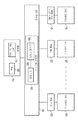
도 1은 상술한 기술들이 구현되어도 되는 시스템의 블록도이다. 다중 처리 디바이스들(10, 20, 30)은, 메모리(70)에 액세스하도록 배치된다. 각 처리 디바이스는, 처리 디바이스에 의해 처리되는 데이터의 로컬 복사본들을 일시적으로 내부에 기억하는 하나 이상의 레벨의 로컬 캐시(15, 25, 35)가 구비될 수도 있다. 각 데이터 값은 상기 메모리(70)내의 메모리 장소를 특정하는 관련 메모리 어드레스를 갖고, 표준 관행에 따라 데이터 값의 복사본은 전형적으로 해당 메모리 어드레스의 표시와 함께 캐시내에 기억된다. 로컬 캐시에서의 데이터가 갱신되면, 예컨대, 해당 데이터에 관해 상기 처리 디바이스에 의해 하나 이상의 기록 연산들이 행해진 결과, 그 갱신된 데이터는 메모리(70)에 역으로 기록될 수 있다. 상기 캐시들은 다양한 방식으로 배치될 수 있다. 예컨대, 캐시가 동시 기록 캐시로서 배치되면, 캐시 라인에 기억된 데이터에 대한 어떠한 갱신도, 갱신을 지연없이 메모리에 복제시키도록 인터커넥트(40)를 거쳐 메모리(70)에 전파된다. 그렇지만, 적어도 하나의 레벨의 로컬 캐시가 라이트백 캐시로서 배치되는 것이 일반적이고, 이때 그 캐시에 보유된 갱신된 버전의 데이터는 메모리에 즉시 전파되지 않는다. 대신에, 더티 플래그는, 메모리보다 더 최신인 데이터를 갖는 캐시 라인들과 관련될 수 있어, 그 캐시 라인 콘텐츠가 이후 상기 캐시로부터 퇴거될 때, 메모리에 대해 필요한 갱신을 할 수 있다. 여기서 설명된 기술들은, 라이트백 캐시로서 배치되는 적어도 하나의 레벨의 로컬 캐시를 갖는 임의의 처리 디바이스에 관련지어 적용되어도 된다. 도 1에서, 상기 캐시(15)는 라이트백 캐시로서 특정되지만, 일 구성 예에서, 로컬 캐시들(15, 25, 35)의 각각은 라이트백 캐시들이어도 된다.
1 is a block diagram of a system in which the above-described techniques may be implemented.
개개의 처리 디바이스들이 그들 각각의 로컬 캐시들(15, 25, 35)에서의 데이터의 복사본들을 국소적으로 캐시할 능력으로 인해, 기록 연산들의 충돌이 동일한 메모리 장소에 관해 상이한 처리 디바이스들내에서 발생하지 않도록 보장하고, 각 처리 디바이스가 공유 데이터의 동일한 뷰를 갖도록 보장하기 위해서, 캐시 일관성 프로토콜을 구현하는 것이 필요하다. 특히, 메모리에 보유된 데이터의 일부가 특별한 처리 디바이스에 따라 다를 수도 있지만, 종종, 그 처리 디바이스들이 메모리에 보유된 데이터의 일부를 공유할 경우이다. 일례로서, 상기 메모리는 공유 데이터베이스(75)를 포함하여도 되고, 각 처리 디바이스는 처리 태스크들이 공유 데이터베이스(75)에 보유된 정보와 관련지어 할당되어도 된다. 공유 데이터베이스에서의 특별한 데이터에 대해 다중 처리 디바이스들에 의해 충돌 갱신들이 행해지지 않도록, 또한 각 처리 디바이스에는 공유 데이터베이스(75)에 보유된 데이터의 일관된 뷰가 제공되도록, 보장하는 것이 중요하다.
Due to the ability of individual processing devices to locally cache copies of data in their respective
일 구성 예에서, 일관성 회로소자(50)는, 캐시 일관성 프로토콜의 적어도 일부를 구현하기 위한 인터커넥트(40)내에 구비될 수 있다. 캐시 일관성 프로토콜을 구현할 때, 착수될 필요가 있는 태스크가 2개인 것이 필수적이다. 특히, 하나의 처리 디바이스가 특별한 메모리 장소에 관해 기록 연산을 수행하고 싶을 때, 기록 연산을 하고 싶은 처리 디바이스가 해당 메모리 장소에 관해 해당 기록 연산을 수행하는 권한을 확립하고 있도록 보장하는 것이 필요하다. 이를 사용하여, 동일한 메모리 장소에 관해 발생하는 기록 충돌 가능성을 피할 수 있다. 게다가, 특별한 메모리 장소에 대한 데이터가 상기와 같은 기록 연산을 거쳐 갱신되어 있으면, 임의의 그 밖의 처리 디바이스가 해당 메모리 장소에 대한 액세스를 요구할 때마다, 갱신된 데이터를 참조하도록 보장하는 것이 중요하다. 따라서, 캐시 일관성 프로토콜의 일부로서, 그 밖의 처리 디바이스들 전부에게 임의의 기록 연산의 결과를 보이도록 보장하는 것이 필요하다.
In one configuration example, coherence circuitry 50 may be provided in
상기 요구된 기능성을 고려하는 캐시 일관성 프로토콜을 완전히 하드웨어로 구현하기 위해 상기 인터커넥트내의 일관성 회로소자를 배치하는 것이 가능하지만, 여기서 기재된 기술들에 따라, 적어도 일부의 메모리 영역들에 대해서, 캐시 일관성 프로토콜의 구현은, 소프트웨어와 하드웨어와의 사이에 분할된다. 특히, 일관성 회로소자(50)는, 기록 연산의 결과로서 하나의 처리 디바이스에서 발생한 갱신된 데이터를 그 밖의 처리 디바이스들에 보이도록 보장하는데 사용될 수 있다. 그렇지만, 데이터를 메모리 장소에 기록하는 권한의 취득은 소프트웨어 프로토콜에 위임되어, 일관성 회로소자(50)는 해당 측면을 고려할 필요가 없다. 보다 상세히 후술하듯이, 소프트웨어 프로토콜은, 분할된 소프트웨어/하드웨어 메카니즘에 의해 제어하는 캐시 일관성을 갖는 메모리 영역내의 메모리 어드레스에 임의의 처리 디바이스가 기록 연산을 수행하기 전에, 해당 처리 디바이스가 관련된 메모리 영역에 관해 소유권 권한을 얻도록 보장하기 위해서, 메모리(70)에 유지된 락(lock)들(80)을 사용한 락 기반 메카니즘을 사용할 수 있다. 이러한 해결방법에 의해, 소프트웨어는 상기와 같은 메모리 영역에 관해 생기는 레이싱 기록 조건들을 피하는 역할을 맡고 있고, 그 후, 일관성 회로소자는 임의의 갱신된 기록 데이터를 그 밖의 처리 디바이스들에 보이게 하기 위해서 하드웨어 프로토콜을 구현한다.
It is possible to place the coherence circuitry in the interconnect to fully implement the cache coherence protocol taking into account the required functionality in hardware, but according to the techniques described herein, for at least some memory regions, the cache coherence protocol The implementation is divided between software and hardware. In particular, the coherence circuitry 50 can be used to ensure that updated data generated in one processing device as a result of a write operation is visible to other processing devices. However, the acquisition of the authority to write data to the memory location is delegated to the software protocol, and the coherence circuit element 50 does not need to consider this aspect. As will be described in more detail later, the software protocol is used to write to a memory address in a memory area with cache consistency controlled by a divided software/hardware mechanism, before any processing device performs a write operation, in a memory area associated with the processing device. In order to ensure that ownership rights are obtained, a lock-based
여기서 설명된 기술에 따라, 하나의 기록 연산, 또는 일부의 경우에 일련의 기록 연산들이 지정된 메모리 영역의 하나 이상의 메모리 장소들내의 갱신된 기록 데이터를 생성하기 위해서 수행되어 있으면, 클린 연산은, 로컬 라이트백 캐시(15)내의 해당 갱신된 기록 데이터를 메모리(70)내의 적절한 메모리 장소들에 전파시키도록 기동된다. 일례에서, 메모리는, 불휘발성 메모리이므로, 상기 시스템내에서의 지속성의 지점을 나타낸다. 특히, 그 데이터가 메모리(70)에 커밋되어 있으면, 해당 데이터는 시스템으로부터 전원을 제거하는 경우에도 유지될 것이다. 따라서, 클린 연산은, 데이터를 상기 시스템내의 지속성의 지점에 전파시킬 수 있다. 그렇지만, 또 하나의 예에서, 상기 메모리는 불휘발성 메모리일 필요는 없다.
In accordance with the technique described herein, if a write operation, or in some cases a series of write operations, is performed to generate updated write data in one or more memory locations of a specified memory area, then the clean operation is a local write operation. It is activated to propagate the corresponding updated write data in the
상술한 기술들에 따라, 일관성 회로소자는, 그 후, 클린 연산의 개시에 응답하여, 기록 데이터를 그 밖의 처리 디바이스들에 보이게 하기 위해서 다수의 일관성 액션들을 취하는 회로소자다. In accordance with the techniques described above, the coherence circuitry is a circuitry that then takes a number of coherence actions to make the write data visible to other processing devices in response to initiation of a clean operation.
예컨대, 처리 디바이스(10)가, 해당 처리 디바이스가 데이터를 제1 메모리 영역에 기록하기 위한 소유권 권한을 확립하기 위해 소프트웨어 프로토콜을 활성화하는 명령을 실행하고 나서, 제1 메모리 영역내의 적어도 하나의 메모리 장소에 대해 하나 이상의 기록 연산들을 수행하여서, 갱신된 기록 데이터를 로컬 라이트백 캐시(15)내에 기억시키는 상황을, 고려한다. 그 후, 처리 디바이스(10)는, 영향을 받은 기록 데이터 전부를 적절한 메모리 장소(들)에 기억하기 위한 메모리(70)에 전파시키기 위해서, 클린연산을 개시시키는 클린 명령을 실행하여도 된다. 그 후, 일관성 회로소자는, 그 밖의 처리 디바이스들(20, 30)이 해당 데이터에의 액세스를 요구하는 경우 상기 갱신된 데이터를 참조하도록 보장하는 그 처리 디바이스들의 로컬 캐시들(25, 35)과 관련지어 단계들을 취함으로써 해당 클린 연산에 응답할 수 있다. 일 시나리오에 있어서, 일관성 회로소자는, 영향을 받은 메모리 장소(들)을 지정하는 각 로컬 캐시(25, 35)에 단지 무효화 요구들을 전파하도록 배치되어도 된다. 그 후, 각 로컬 캐시는, 각기 지정된 메모리 장소에 관해 검색을 수행하여 해당 메모리 장소에 대한 상기 캐시에 엔트리가 존재하는지를 판정한다. 존재할 경우, 그 후, 현재의 콘텐츠는 로컬 캐시내에서 무효화될 것이다. 이것은, 이후에 처리 디바이스가 해당 메모리 어드레스에서의 데이터에 대해 요구를 하면, 로컬 캐시에서 미스를 검출하여, 그 후 그 데이터가 메모리로부터 얻게 된 결과, 정확한 데이터가 처리 디바이스(20, 30)에 의해 수신되도록 보장할 것이다.
For example, after the
간단한 구성에 있어서 일관성 회로소자가 무효화 요구들을 그 밖의 로컬 캐시들 전부에 방송할 수도 있지만, 다른 실시예에서, 일관성 회로소자는, 스누프 제어기(55)와 관련 디렉토리(60)를 포함하는, 스누프 회로소자의 형태를 취할 수도 있다. 이 디렉토리는, 각 로컬 캐시(15, 25, 35)에 의해 데이터가 캐시되는 메모리 장소들을 표시하도록, 상기 스누프 제어기에 의해 유지된다. 이에 따라, 클린 연산에 의해 영향을 받은 메모리 장소나 메모리 장소들에 관하여, 스누프 제어기(55)는, 각종 로컬 캐시들 중 어느 로컬 캐시가 상기 영향을 받은 데이터의 캐시된 로컬 복사본을 가질지도 모르는 것을 특정하기 위해 상기 디렉토리내에서 검색을 수행할 수 있으므로, 단지 무효화 요구를 캐시마다 방송하는 대신에 관련 캐시들에 대한 무효화 요구들을 표적으로 삼을 수 있다.
Although in a simple configuration the coherence circuitry may broadcast invalidation requests to all other local caches, in other embodiments, the coherence circuitry includes a snoop
이러한 해결방법에 의해 알 수 있는 것은, 일관성 회로소자가, 상기 갱신된 기록 데이터가 메모리에 기록되는 지점에서, 처리 디바이스들 전부가 해당 데이터의 일관된 뷰를 갖는 것이 보장될 수 있도록 보장하기 위해 클린 연산에 응답할 수 있다는 것이다. What can be seen by this solution is that the coherence circuitry, at the point where the updated write data is written to memory, is a clean operation to ensure that all of the processing devices have a consistent view of that data. Is that you can respond to.
클린 연산이 수행되기 전의 기간에, 또한 처리 디바이스(10)가 하나 또는 메모리 장소들에 대한 갱신된 기록 데이터를 발생하기 위해 하나 이상의 기록 명령들을 실행중인 동안에, 소프트웨어 프로토콜은 그 밖의 처리 디바이스들에 의해 그 하나 이상의 메모리 장소들에의 액세스를 규제할 수 있다. 일부의 경우에, 의도된 상기 데이터의 소프트웨어 사용은 소프트웨어 프로토콜에 의해 또 하나의 처리 디바이스가 데이터의 오래된 값을 메모리로부터 판독할 수 있기 위한 것이고, 그 밖의 경우에는, 상기와 같은 판독연산이 그 때에 금지될 수도 있다.
In the period before the clean operation is performed, and while the
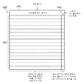
도 2는 도 1의 디렉토리(60)의 일 구성 예를 개략적으로 도시하는 도면이다. 본 예에서, 상기 디렉토리는 다수의 엔트리들(100, 105)을 갖고, 각 엔트리는, 하나의 메모리 어드레스나, 일련의 메모리 어드레스들을 특정하고 나서, 해당 메모리 어드레스 또는 일련의 메모리 어드레스들내의 데이터의 복사본을 캐시들이 가질 수도 있는 것을 특정한다. 이것은, 스누프 제어기에 의해, 앞서 언급된 클린 연산에 응답하여 로컬 캐시들에 대해 무효화 연산이 실시될 필요가 있는지를 판정하는데 사용될 수 있다. 도 2의 예에서, 체크 표시는 관련된 캐시가 캐시된 복사본을 보유할 수도 있는 것을 나타내는데 사용되고, X표는 관련된 캐시가 복사본을 보유하지 않는 것을 나타내는데 사용된다. 그 체크 표시와 X표가 임의의 적절한 값으로 인코딩될 수 있고, 예컨대, 논리 1값이 체크 표시를 나타내고 논리 0값이 X표를 나타낼 수도 있다는 것을 알 것이다.
FIG. 2 is a diagram schematically showing an example of the configuration of the
도 2는 단지 디렉토리(60)의 일 구성 예를 도시하는 것일 뿐이고, 임의의 그 밖의 적절한 구성은 수신된 클린 연산에 응답하여 캐시들에 대해 무효화 연산들이 실시될 필요가 있는 것에 관해 상기 스누프 제어기에 정보를 제공하는데 사용될 수 있었다는 것을 알 것이다.
Fig. 2 is only to show an example configuration of
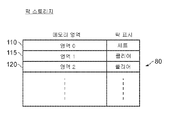
도 3은 사용될 수 있는 락 스토리지(80)의 구성 예를 도시한 것이다. 락 스토리지는, 각각 특별한 메모리 영역에 관계하는 복수의 엔트리들(110, 115, 120)을 가질 수 있다. 락 표시는, 메모리 영역마다 해당 영역내의 적어도 하나의 메모리 어드레스가 그의 데이터 값을 갱신시키는 중인지를 특정하는데 유지될 수 있다. 락 표시가 세트일 경우, 이것은 상기 영역내의 적어도 하나의 메모리 어드레스에 대한 데이터가 갱신중인 것을 나타내는 반면에, 락 표시가 클리어일 경우, 이것은 상기 영역내의 어드레스들 중 아무것도 갱신되는 중인 데이터를 포함하지 않는 것을 나타낸다.
3 shows an example of a configuration of a
처리 디바이스가 락 스토리지에 의해 통제된 영역들 중 하나의 영역내의 메모리 어드레스에 관해 기록 연산을 수행하고 싶을 때, 해당 처리 디바이스에 의해 상기 관련된 락 표시를 설정하려고 시도하기 위해서 명령을 실행할 것이다. 그 관련된 락 표시가 현재 클리어일 경우, 그것은 설정되고, 확인응답은 처리 디바이스에 회신될 것이고, 이것은, 처리 디바이스가 지금 그 관련된 메모리 영역에 대한 소유권 권한을 확립하고 있음에 따라, 해당 메모리 영역에 관해 기록 연산을 자유롭게 수행하는 것을, 실제로 상기 처리 디바이스에 대해 특정한다. 그렇지만, 락 표시가 이미 세트일 경우, 처리 디바이스는, 락을 설정하려고 시도하고 있는 중인 명령 이후에 계속되지 않게 되고, 특히, 해당 스테이지에서 관련 영역내의 메모리 어드레스에 기록하려고 시도하는 임의의 기록 명령들 실행하면 안될 것이다. 일례에서, 관련 영역에 대한 락 표시가 클리어 상태로 복귀되는 시간, 그 시점에서, 락 표시가 다시 설정될 수 있을 때까지 실행은 일시 중지될 것이고, 처리 디바이스가 메모리 영역에 관해 지금 소유권 권한을 갖는 것을 특정하기 위해 상기 처리 디바이스에 발행된 확인응답 그 이후, 기록 명령(들)이 실행될 수 있다. 이러한 해결방법에 의해, 소프트웨어 프로토콜은, 임의의 특별한 시점에서, 단지 하나의 처리 디바이스만이 이러한 각 영역내의 메모리 장소에 관해 기록 연산들을 수행할 권한이 주어지도록 보장하기 위해서, 복수의 메모리 영역들에 대한 소유권 권한을 유지하는데 사용될 수 있다. 이것은 일관성 회로소자(50)의 요구된 연산들을 단순화하는데, 그 이유는, 특별한 처리 디바이스에 의해 배타적 소유권을 보장하도록 임의의 단계들을 취할 필요가 없고, 대신에 단지 이후의 클린 연산들에 응답하면 되어 처리 디바이스들이 데이터가 갱신되어 있은 후 그 데이터의 일관된 뷰를 갖도록 보장하기 때문이다. When a processing device wants to perform a write operation on a memory address in one of the areas controlled by the lock storage, it will execute an instruction to attempt to set the associated lock indication by that processing device. If the associated lock indication is currently clear, it will be set, and an acknowledgment will be returned to the processing device, which, as the processing device is now establishing ownership rights for that associated memory area, for that memory area. It actually specifies for the processing device to freely perform the write operation. However, if the lock indication is already set, the processing device will not continue after the instruction being attempted to set the lock, in particular any write instructions attempting to write to a memory address in the relevant area at that stage. It shouldn't be done. In one example, the time at which the lock indication for the relevant area returns to the clear state, at which point execution will be paused until the lock indication can be set again, and the processing device now has ownership rights on the memory area. After the acknowledgment issued to the processing device to specify that, the write command(s) may be executed. By this solution, the software protocol is applied to multiple memory areas, to ensure that at any particular point, only one processing device is authorized to perform write operations on the memory locations within each of these areas. It can be used to maintain ownership rights. This simplifies the required operations of the coherence circuitry 50, because there is no need to take any steps to ensure exclusive ownership by a special processing device, but instead just respond to subsequent clean operations. This is because it ensures that processing devices have a consistent view of the data after it has been updated.
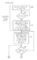
도 4a 및 4b는, 처리 디바이스가, 조합된 소프트웨어/하드웨어 메카니즘을 사용하여 캐시 일관성을 구현하는 특별한 메모리 영역내의 데이터를 갱신하고 싶을 때, 일 구성 예에서 해당 처리 디바이스내에서 수행된 단계들을 도시하는 흐름도를 제공한다. 4A and 4B illustrate the steps performed in the processing device in one configuration example when the processing device wants to update data in a special memory area that implements cache coherence using a combined software/hardware mechanism. Provides a flow chart.
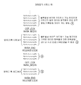
단계 200에서, 겟(get) 락 명령은, 원하는 메모리 영역에 관해 처리 회로소자에 의해 실행된다. 이것은 그 메모리내의 락들(80)이 액세스되게 하고, 특히 관련 영역에 대한 락 표시 상태가 평가되게 한다. 락 표시가 이미 세트일 경우, 상기 처리는, 단계 205에서, 락 표시가 현재 클리어라고 판정되는 시간, 그 시점에서 락 표시는 상기 처리 디바이스에 의해 겟 락 명령을 실행함으로써 락이 얻어진 것을 나타내도록 설정될 수 있을 때까지 일시 중지된다. 상기 락이 얻어지면, 이것은, 사실상, 요구하는 처리 디바이스가, 단계 210에 의해 나타낸 것처럼, 원하는 메모리 영역내의 장소들에 데이터를 기록하기 위한 소유권 권한을 확립하였다는 것을 의미한다. 이 스테이지에서, 소프트웨어 프로토콜은, 그 밖의 처리 디바이스들이 당해 메모리 영역에 기록 액세스하는 것을 방지하는데, 그 이유는 그들의 그 밖의 처리 디바이스들 중 어느 하나가 겟 락 명령을 실행하기 위한 것이면, 락 표시가 이미 세트이라고 판정됨에 따라서, 그들이 해당 메모리 영역에 대한 락을 얻을 수 없을 것이기 때문이다. 따라서, 단계 200, 205, 210은, 데이터를 기록하는 권한을 확립하는 소프트웨어 프로토콜을 구현하는 것으로서 보여질 수 있다.
In
단계 210 후에, 단계 215에서, 처리 디바이스는, 락 걸린(locked) 메모리 영역내의 메모리 장소들에 대한 기록 데이터를 발생하기 위해서, 하나 이상의 기록 연산들을 행할 수 있고, 이때의 발생된 기록 데이터는 처리 디바이스의 로컬 라이트백 캐시에 기억된다. 이 처리는, 클린 연산에 대한 기동이 단계 220에서 검출될 때까지 계속될 수 있다.
After
일 구성 예에서, 클린 연산에 대한 기동이 다양한 이유로 일어날 수 있다. 예를 들면, 단순한 경우에 있어서, 별도의 클린 명령은 각 기록 명령과 관련되어도 되어, 수행된 처리는 처리 디바이스가 그 락을 얻고 나서, 단일의 기록 연산을 원하는 메모리 장소에 대해 수행하기 위한 것이고, 그 후 클린 명령이 해당 기록 데이터에 관해 클린 연산을 기동하도록 실행되기 위한 것이다. 그렇지만, 또 하나의 구성 예에서는, 락 걸린 메모리 영역내의 메모리 어드레스들에 관해 일련의 기록 연산들을 함께 분류하는 것이 가능할 수도 있고, 이때의 단일의 클린 연산은 그 기록 연산들이 수행된 후 기동된다. 예를 들면, 이러한 기능성을 달성하기 위한 하나의 적절한 메카니즘은, 공통으로 소유한 동시계류중인 미국특허출원 번호 15/501,278에 기재된 메카니즘이고, 이로써 그 메카니즘의 전체 내용은, 참조로 포함되어 있다. 특히, 거기에 정의된 종료 명령은 클린 명령으로서 사용되어 클린 연산을 기동할 수 있고, 원하는 경우, 관련된 시작 명령은, 종료 명령에 접할 때 클린될 필요가 있는 기록 데이터를 갖는 기록 명령들의 시퀀스의 시작을 확인하는데 사용될 수 있다. 별도의 스토리지 구조는, 그 종료 명령에 응답하여 클린될 필요가 있는 메모리 장소들을 추적하게 유지될 수 있다. In one configuration example, activation for a clean operation may occur for a variety of reasons. For example, in a simple case, a separate clean instruction may be associated with each write instruction, and the processing performed is to perform a single write operation to the desired memory location after the processing device acquires the lock, After that, the clean instruction is to be executed to start a clean operation on the corresponding record data. However, in another configuration example, it may be possible to classify a series of write operations together for memory addresses in the locked memory area, and a single clean operation at this time is started after the write operations are performed. For example, one suitable mechanism for achieving this functionality is the one described in commonly owned co-pending U.S. Patent Application No. 15/501,278, whereby the entire contents of that mechanism are incorporated by reference. In particular, the end instruction defined therein can be used as a clean instruction to initiate a clean operation, and, if desired, the associated start instruction, the start of a sequence of write instructions with write data that needs to be cleaned when contacting the end instruction. Can be used to check. A separate storage structure can be maintained to keep track of memory locations that need to be cleaned in response to the shutdown command.
단계 220에서 생길 수 있는 기동의 또 추가의 예로서, 이것은, 단계 215에서 수행된 기록 연산에 의해 생성된 갱신된 기록 데이터를 갖는 캐시 엔트리를 표적으로 삼는 퇴거 이벤트이어도 된다. 퇴거 이벤트는 예를 들면, 로컬 캐시내의 용량 문제들로 인해 생길 수도 있고, 여기서 빅팀 엔트리는 새로운 데이터가 상기 캐시에 할당될 공간을 만드는데 선택될 필요가 있다. 그 빅팀 엔트리가 단계 215에서 생성된 기록 데이터를 갖는 엔트리일 때, 이것은 단계 220에서 클린 연산을 기동할 수 있다. 일련의 기록 연산들이 시작 명령 및 종료 명령과 관련되는 앞선 구성 예를 이용하면, 상기 영??을 받은 캐시 엔트리들 중 하나에 관해 퇴거는, 클린연산을 적어도 해당 엔트리에 관해 기동시키는데 사용될 수 있거나, 원하는 경우, 퇴거 기동이 발생할 때 상기 시작 명령과 종료 명령의 사이에서 기록 데이터가 생성되어 있는 엔트리들 전부를 클리닝시킬 수 있다.
As another further example of an activation that may occur in
기동 이벤트가 단계 220에서 일어날 때, 처리는 단계 225로 진행되어, 메모리 콘텐츠를 갱신시켜 기록 연산(들)에 의해 생성된 상기 갱신된 데이터를 반영하도록, 락 걸린 메모리 영역에 관해 생성되어 있는 기록 데이터에 대해 클린 연산이 행해진다.
When the start-up event occurs in
앞서 설명된 것처럼, 일관성 회로소자(50)는, 상기와 같은 클린 연산의 존재에 응답하여, 메모리에 기록중인 기록 데이터를 처리 디바이스들 전부에 보이게 되도록 보장하기 위해서 그 밖의 처리 디바이스들의 로컬 캐시들에서의 임의의 관련 엔트리들에 관해 무효화 연산들을 수행할 것이다. 단계 230에서, 요구된 메모리 영역에 대한 락을 얻은 처리 디바이스는, 일관성 회로소자로부터 기록 데이터가 그 밖의 처리 디바이스들에게 보인다는 확인을 기다린다. 다중 캐시 엔트리들이 클린 처리동안에 클린되어도 되는 상황들에 있어서, 단계 230에서는, 관련 기록 데이터 전부가 그 밖의 처리 디바이스들에게 보이고 있다는, 즉 요구된 무효화 연산들 전부가 수행되어 있다는 확인을 기다릴 것이다.
As previously described, the coherence circuitry 50, in response to the presence of such a clean operation, in the local caches of other processing devices to ensure that the write data being written to the memory is visible to all of the processing devices. Will perform invalidation operations on any relevant entries of. In
이러한 확인을 단계 230에서 수신하면, 클린 연산은 완료되고, 단계 235에서는 수행될 기록 연산들 또는 클린 연산이 더 있는지를 판정한다. 이것은, 예컨대, 락을 해제시키는 실행을 갖는 명령에 앞서 명령 시퀀스에서의 하나 이상의 추가의 기록 명령들이나 클린 명령들이 있는 경우라고 판정될 수 있다. 수행될 적어도 하나 더 기록 연산이나 클린 연산이 있을 경우, 처리는 단계 220으로 진행되어 또 하나의 클린 연산에 대한 기동이 있는지를 판정하고, 기동이 없을 경우 처리는 단계 215로 복귀되어 하나 이상의 추가의 기록 연산들을 수행한다.
Upon receiving this confirmation at
단계 235에서 더 이상 수행될 기록 연산 또는 클린 연산이 없는지를 판정하면, 그 후, 처리 회로소자는, 단계 240에서 메모리 영역에 대한 락을 해제하는 해제(release) 락 명령을 실행하도록 배치되어도 된다. 이것은, 해당 영역에 대한 락 표시를 클리어 상태로 리셋하기 위해서 락 스토리지(80)에서의 적절한 엔트리에의 액세스를 수행함으로써 이루어진다.
If it is determined in
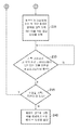
도 5는 일례에서 일관성 회로소자(50)의 연산을 도시하는 흐름도다. 단계 300에서, 일관성 회로소자(50)는, 도 4a 및 4b를 참조하여 앞서 설명된 단계들을 수행중인 처리 디바이스로부터의 클린 연산의 통지를 기다린다. 클린 연산의 통지시, 일관성 회로소자에 의해, 메모리 콘텐츠를 갱신시키도록 단계 305에서 관련된 기록 데이터는 메모리(70)에 전파된다. 병렬로, 처리가 단계 310으로 진행되어, 만약에 있다면, 그 밖의 캐시들이 클린 연산과 관련된 메모리 어드레스에 대한 데이터를 기억할 수도 있는지를 특정하기 위해서 상기 디렉토리(60)를 참조한다. 그 후, 스누프 제어기(55)는, 단계 315에서 디렉토리 정보로 나타낸 각 캐시에 무효화 요구를 보내도록 배치된다. 무효화 요구는, 당해 메모리 어드레스를 특정하고, 해당 무효화 요구를 수신하는 로컬 캐시가 검색연산을 수행하게 하여 실제로 해당 메모리 어드레스에서의 데이터의 복사본을 캐시하는 엔트리가 있는지를 확인하여, 있을 경우 해당 엔트리는 무효화될 것이다. 이것은, 관련된 처리 디바이스가 해당 메모리 어드레스에서의 데이터를 요구하면 더 이상 로컬 캐시내의 히트를 수신하지 않고, 대신에 정확한 데이터가 메모리(70)로부터 검색되도록, 보장할 것이다.
5 is a flow chart showing the operation of the coherence circuit element 50 in one example. In
단계 315에서의 상술한 예에서는 무효화 요구들이 스누프 제어기(55)에 의해 관련 로컬 캐시들에 보내지지만, 다른 해결방법에서는, 갱신 요구들은, 정확히 요구된 데이터를 반영하기 위해 로컬 캐시 콘텐츠를 갱신시키도록, 새로운 기록 데이터와 함께 보내질 수 있었다.
In the above example in
단계 320에서, 스누프 제어기(55)는, 요구된 무효화 전부가 발생하였다는 확인을 기다린다. 해당 확인이 수신되었다면, 단계 325에서, 스누프 제어기는, 클린 연산을 개시한 처리 디바이스에, 그 데이터가 지금 그 밖의 처리 디바이스들에 보인다는 것을 특정하도록 통지할 수 있다. 단계 310에서 상기 디렉토리가 그 밖의 캐시들 중 아무도 상기 요구된 메모리 어드레스에 대한 데이터를 기억하지 않을 수도 있는 것을 나타내면, 처리는 단계 310으로부터 단계 325로 직접 진행될 수 있다는 것을 주목해야 한다.
In
클린 연산이 다중 메모리 어드레스들에 관해 적용되는 경우들, 이를테면 이것은 앞서 언급된 시작 명령과 종료 명령을 사용할 때의 경우에, 무효화 요구들은 상기 갱신된 캐시 라인 콘텐츠의 각각에 대한 상기 요구된 캐시들에 보내질 수 있고, 단계 320에서 스누프 제어기는, 단계 325로 진행되기 전에 상기 갱신된 데이터 값들 전부에 관해 상기 요구된 무효화 전부가 발생하였다는 확인을 기다린다.
In cases where a clean operation is applied for multiple memory addresses, such as this is the case when using the aforementioned start command and end command, invalidation requests are made to the requested caches for each of the updated cache line contents. Can be sent, and at
단계 310 내지 325는, 전체적으로 일관성 회로소자(50)에 의해 개시되고, 소프트웨어 프로그래머에게 어떠한 가시성도 요구하지 않고, 특히 상기 처리 디바이스들 중 어느 하나에 의해 실행될 어떠한 명시적 명령들도 요구하지 않는다는 것을 알 것이다. 따라서, 단계 310 내지 325는 상기 처리 디바이스 전부에 기록 데이터를 보이게 하도록 하드웨어 프로토콜을 구현한다는 것을 알 수 있다.
It should be noted that
단계 305에서 출력된 데이터를 실제로 메모리에 기록하는 것이 많은 클록 사이클이 걸릴 수도 있지만, 기록 데이터는, 전형적으로 상기 캐시로부터 인터커넥트(40)에 전파된 직후 일관성의 지점(예컨대, 메모리에 대한 인터페이스와 관련된 하나 이상의 기록버퍼들)에 도달할 것이다. 도 5에서는, 일관성의 지점에, 적어도 단계 310에서의 체크가 수행되었을 때까지 도달된다고 가정하고, 이에 따라 단계 325에 도달될 때까지, 기록 데이터는 아직 메인 메모리에 역으로 기록되지 않은 경우에도, 상기 일관성의 지점으로부터 이용 가능할 것이라고 이해된다.
Although it may take many clock cycles to actually write the data output in
상기 요구된 캐시 일관성 프로토콜을 구현하기 위해 소프트웨어 프로토콜과 하드웨어 프로토콜의 조합을 이용하는 상술한 메카니즘이 처리 디바이스간에 공유될 수도 있는 상기 메모리(70)의 메모리 영역 전부에 관해 구현될 수 있지만, 다른 예에서 이러한 해결방법은 일부의 영역들에 사용되어도 되지만, 풀 하드웨어 캐시 일관성은 원하는 경우 기타의 영역들에 대해 구현되어도 된다. 이것은, 도 6의 흐름도로 개략적으로 나타내어진다. 특히, 단계 350에서는, 당해 영역이 풀 하드웨어 일관성을 요구하는지를 판정한다. 요구할 경우, 처리는 단계 355로 진행되어 일관성 회로소자를 사용하여 캐시 일관성 프로토콜을 하드웨어로 완전히 구현한다. 특히, 처리 디바이스들 전부에 갱신된 데이터가 보이도록 보장하기 위해서, 클린 연산에 응답하여 상술한 단계들을 구현할 뿐만 아니라, 임의의 처리 디바이스가 기록 연산을 수행하기 전에, 기록 연산을 수행하고 싶은 처리 디바이스가 해당 처리 디바이스에 대해 배탁적인 것으로서 표시되는 캐시된 복사본을 갖도록 보장하기 위해 로컬 캐시들에 관해 일관성 액션들을 수행하기도 하는, 기존의 스누프 메카니즘들을 사용할 수 있다. 따라서, 이러한 해결방법은, 데이터를 기록하는 권한의 확립이 일관성 회로소자(50)에서 수행한 하드웨어 프로토콜내에 내장되는 것을 가능하게 한다. 공지된 하드웨어 캐시 일관성 기법은, 단계 355에서 사용될 수 있다.
The above-described mechanism using a combination of a software protocol and a hardware protocol to implement the requested cache coherence protocol may be implemented for all of the memory areas of the
그렇지만, 상기 영역이 풀 하드웨어 일관성을 요구하지 않으면, 처리는 단계 360으로 진행되어 그 영역에 기록할 권한은, 메모리(70)에서 락들(80)을 참조하여 앞서 설명된 소프트웨어 프로토콜 기술을 사용하여 관리된다. 그 후, 단계 365에서, 갱신된 기록 데이터가 처리 디바이스 전부에 보이게 하는데 요구된 단계들은, 앞서 설명된 하드웨어 프로토콜을 사용하여 관리되고, 일관성 회로소자(50)에 의해 구현된다.
However, if the area does not require full hardware consistency, processing proceeds to step 360, and the authority to write to the area is managed using the software protocol technique described above with reference to the
도 7a 내지 7d는, 소프트웨어 프로토콜과 하드웨어 프로토콜을 조합으로 사용하여 캐시 일관성을 구현하는 상황들에 있어서 로컬 라이트백 캐시를 갖는 처리 디바이스에 의해 실행되어도 되는 명령 시퀀스들의 예를 도시한 것이다. 도 7a에 도시된 것처럼, 단일의 기록 명령과 관련 클린 명령은, 상기 겟 락 명령과 상기 해제 락 명령의 사이에서 실행되어도 된다. 다른 구성에서는, 도 7b에 도시된 것처럼, 앞서 언급된 시작 명령과 종료 명령을 사용하여 기록 명령들의 그룹을 특정할 수 있고, 이때의 종료 명령은 상기 일련의 기록 명령들에 의해 생성된 기록 데이터 전부에 관해 클린 연산을 개시하는데 사용된다. 도 7c 및 7d는 도 7a에 도시된 구성의 변형 예로, 특히 다중 기록 명령들 및 관련 클린 명령이 겟 락 명령과 해제 락 명령의 사이에서 실행되는, 추가의 다른 구성들을 도시한 것이다. 도 7d로부터, 특별한 기록 명령과 관련된 클린 명령이 반드시 상기 시퀀스에서의 기록 명령에 바로 후속할 필요는 없다는 것을 주목해야 한다. 7A to 7D show examples of instruction sequences that may be executed by a processing device having a local writeback cache in situations where cache coherence is implemented using a combination of a software protocol and a hardware protocol. As shown in Fig. 7A, a single write command and related clean command may be executed between the get lock command and the release lock command. In another configuration, as shown in Fig. 7B, a group of recording commands can be specified using the above-mentioned start command and end command, and the end command at this time is all of the record data generated by the series of write commands. Is used to initiate a clean operation on 7C and 7D show a variant of the configuration shown in FIG. 7A, in particular, in which multiple write commands and related clean commands are executed between a get lock command and a release lock command. It should be noted from Fig. 7D that the clean command associated with a special write command does not necessarily immediately follow the write command in the sequence.
앞서 언급된 것처럼, 앞서 언급된 시작 명령과 종료 명령이 사용되는 구성 예에 있어서, 기억유닛은, 시작 명령과 종료 명령의 사이에서 처리 디바이스에 의해 수행된 기록 연산들의 표시들을 유지하도록, 이러한 시작 및 종료 명령을 포함하는 명령들의 시퀀스를 실행하는 상기 처리 디바이스와 관련지어 제공되어도 된다. 도 8은 FIFO 기억 회로소자(450)의 형태를 취하는 상기와 같은 기억유닛의 일 구성 예를 도시한 것이다.
As mentioned above, in the configuration example in which the above-mentioned start command and end command are used, the storage unit keeps indications of write operations performed by the processing device between the start command and the end command, It may be provided in association with the processing device that executes a sequence of instructions including an end instruction. 8 shows an example of the configuration of the storage unit as described above, which takes the form of a FIFO
시작 명령과 종료 명령 사이에 끼어 있는 기록 명령에 접할 때, 처리 디바이스는, FIFO 제어(448)와, 이 기록 명령에 응답하여 행해지는 기록 연산의 표시가 FIFO 스토리지(446)의 엔트리에 부가되어야 하는 상기 관련된 라이트백 캐시에 대해, 가리킨다. 도 8은 FIFO 스토리지(446)의 4개의 엔트리가 현재, 기록 연산 A-D의 표시로 채워지는 구성 예를 도시한 것이다. 본 도면에 나타낸 것처럼, 이 표시들은, 기록 연산들의 타겟 메모리 어드레스들(또는, 실제로, 라이트백 캐시에서의 대응한 엔트리를 특정하기에 충분한 일부 메모리 어드레스들만)을 포함할 수 있거나, 그 대신에, 대응한 엔트리가 라이트백 캐시에서 발견될 경우를 도시하는 캐시 블록 지시자들이어도 된다. FIFO 제어유닛(448)은, 요구된 대로, 엔트리들의 부가 및 엔트리들의 삭제(개별적으로 또는 FIFO의 전체 콘텐트)를 관리하는 FIFO 스토리지(446)의 전반적인 제어를 유지한다. FIFO 기억 회로소자(450)가, 라이트백 캐시에서의 특별한 데이터 항목이 FIFO 스토리지(446)에서의 대응한 엔트리를 갖는지에 관해 라이트백 캐시로부터의 질의에 응답하도록 요구되는 경우, FIFO 기억 회로소자(450)는 이 기능성을 제공하도록 콘텐트 어드레스 가능 방식으로 구성될 수 있다. 이러한 개별적인 질의가 수신될 수도 있을 때의 일례는, 라이트백 캐시로부터의 데이터 항목의 퇴거상에 있고, 이에 응답하여, FIFO 제어(448)는 FIFO 스토리지(446)에서의 대응한 엔트리를 제거시키도록 구성될 수 있다. 또는, 라이트백 캐시로부터의 콘텐트 질의는, 캐시 일관성 메카니즘의 참여의 일부로서 상기 라이트백 캐시에 의해 수신된 스누프 질의에 응답하여 수신되어도 된다, 하지만 도 9를 참조하여 후술하듯이, 라이트백 캐시 자체는, FIFO 스토리지(446)에 이 콘텐트 어드레스 가능 메모리 구성이 제공될 필요성을 피하므로 상기 처리 디바이스에 상대적으로 작은 부가로서 FIFO 스토리지(446)의 제공을 용이하게 하기 위해서, 대응한 엔트리가 현재 FIFO 스토리지(446)에 보유되는지 여부의 표시를 기억하도록 구성되어도 된다. 끝으로, 도 8에 도시된 것처럼, FIFO 제어(448)는, 한층 더, FIFO 스토리지(446)가 완전히 채워지는(이 때문에 추가의 엔트리들이 만들어질 수 없을)지를 감시하도록 구성된다. FIFO 스토리지(446)가 완전히 채워지는 경우에, FIFO 제어(448)는, 이 사실의 신호를 라이트백 캐시에 보내고 나서, 라이트백 캐시에서의 대응한 엔트리들을 메모리(70)에 재빠르게 역으로 기록시키고, 그 FIFO 스토리지(446)의 콘텐트는 클리어된다.
When contacting the write command sandwiched between the start command and the end command, the processing device must have the
도 9는, 이 라이트백 캐시가 제어기(460)와 다수의 캐시 라인들(462)을 갖는 것을 도시하는, 라이트백 캐시(432)를 개략적으로 도시한 것이다. 캐시 제어기(460)는, 상기 관련된 처리 디바이스로부터 수신된 데이터 항목들과 제어신호들을 감시하고, 이때의 제어신호들은 처리 디바이스의 파이프라인과 FIFO 제어(448)와의 양쪽으로부터 수신된다. 캐시 라인들(462)은 처리 디바이스의 데이터 처리 연산에 있어서 처리 디바이스에서 사용한 데이터 항목들을 기억하도록 구성되고, 각 캐시 라인은 데이터 항목 자신들과 관련 상태 마커들(통상의 방식으로 더티/유효 등)의 양쪽을 기억한다. 그렇지만, 추가로, 여기서는 각 캐시 라인의 하나의 비트를, 클린 온 스누프(clean-on-snoop) 마커로서 취급될 수 있는 전용 마커(464)로서 정의하고, 캐시 라인들(462) 중 하나에서 히트하는 또 하나의 캐시/CPU로부터 스누프가 수신되면, 마커(464)의 존재는 해당 캐시 라인이 메모리에 대해 클린되게 한다는 것을 주목한다. 캐시 라인의 퇴거는 단지 일례일 뿐이고, 따라서 상기 마커(464)는 클린 온 퇴거(clean-on-evict) 마커로서 보여질 수 있다. 도시된 구성에 있어서, 캐시 제어기(460)는 상기 시스템에서 그 밖의 캐시들로부터 수신된 스누프들을 감시하도록 구성되고, 상기 마커(464)가 세트인 캐시(432)의 캐시 라인(462)에 기억된 데이터 항목에 관한 또 하나의 캐시로부터의 스누프가 수신될 때, 캐시 제어기(460)는 즉시 해당 캐시 라인을 퇴거시키도록 구성된다. 또한, 이 이벤트는, FIFO 스토리지(446)에서의 임의의 대응한 콘텐트가 클리어될 수 있도록 FIFO 제어(448)에 신호로 보내진다.
9 schematically shows a
도 10은 일례에서 처리 디바이스에 의해 실행되어도 되는 명령들의 시퀀스의 예를 도시한 것이다. 이 경우에는, 상기 시작 명령과 종료 명령을 사용하여, 상기 시스템내의 지속성의 지점을 형성하는 불휘발성 메모리에 대해 수행되는 일련의 기록들을 특정한다고 가정한다. 특히, 그 불휘발성 메모리는 불휘발성 바이트 어드레스 가능(NVBA) 메모리이어도 된다. (A라고 붙여진) 상기 시퀀스의 제1 부분은, 불휘발성 바이트 어드레스 가능 메모리에 기억되지 않은 데이터 항목들에 액세스하는 판독 명령, 기록 명령 및 데터 처리 명령에 관계하는 다수의 명령들을 갖는다. 그 후, 상기 판독 명령, 데이터 처리 명령 및 기록 명령이 불휘발성 바이트 어드레스 가능 메모리에 기억되는 데이터 항목들에 (적어도 부분적으로) 관계하는 제1 영역(기록 세트)의 시작을 정의하는 nvba_begin 명령(앞서 언급된 시작 명령의 일례)이 뒤이어 있다. 이 제1 영역(기록 세트)(B라고 붙여진)은 nvba-end 명령(앞서 언급된 종료 명령의 일례)으로 종료된다. 그 후, 불휘발성 바이트 어드레스 가능 메모리에 기억된 데이터 항목들에 관계하지 않는 제2 세트의 명령들(A)이 뒤이어 있다. 끝으로, 불휘발성 기록 어드레스 가능 메모리에 기억된 데이터 항목들에 (적어도 부분적으로) 관계하는 판독 명령, 데이터 처리 명령 및 기록 명령(B)의 제2 영역(기록 세트)는, 제2 nvba_begin 명령과 제2 nvba_end 명령에 의해 정의된다. 상기 nvba_begin 명령과 nvba_end 명령의 제공에 의해 프로그래머는 기록 세트들을 정의할 수 있고, (서로에 대해) 본 기술들이 보존할 수 있는 오더링은, 액세스된 데이터 항목들이 불휘발성 메모리에 기억될 때에도, 라이트백 캐시에 의해 캐시되는 액세스를 보존할 수 있다. 10 shows an example of a sequence of instructions that may be executed by the processing device in an example. In this case, it is assumed that the start command and the end command are used to specify a series of writes to be performed on the nonvolatile memory forming a point of persistence in the system. In particular, the nonvolatile memory may be a nonvolatile byte addressable (NVBA) memory. The first part of the sequence (labeled A) has a number of instructions relating to a read command, a write command and a data processing command to access data items not stored in the nonvolatile byte addressable memory. Then, the nvba_begin command (prior to An example of the mentioned start command) follows. This first area (recording set) (labeled B) ends with the nvba-end command (an example of the previously mentioned end command). This is followed by a second set of instructions A that do not relate to data items stored in the nonvolatile byte addressable memory. Finally, the second area (write set) of the read command, data processing command, and write command (B) related (at least partially) to the data items stored in the nonvolatile write addressable memory is a second nvba_begin command and It is defined by the second nvba_end command. By providing the nvba_begin command and the nvba_end command, the programmer can define record sets, and the ordering that these techniques can preserve (for each other) is writeback, even when accessed data items are stored in nonvolatile memory. You can preserve access that is cached by the cache.
여기서 설명된 기술들에 따라, 상기 시작 및 종료 명령에 의해 특정된 각 블록 전에 겟 락 명령이 있고, 각 블록 후에 해제 락 명령이 있어서, 앞서 언급된 소프트웨어 프로토콜 메카니즘은, 기록 연산들 중 어느 하나를 수행하기 전에 기록할 권한을 처리 디바이스가 얻도록 보장하는데 사용될 수 있다. 그 결과, 그 후 일관성 회로소자에 의해 증분된 하드웨어 프로토콜은, 단지, 종료 명령에 의해 기동된 클린 연산이 발생하면 각종 그 밖의 처리 디바이스들에 해당 기록 데이터를 보이게 하도록, 보장하면 된다. According to the techniques described herein, there is a get lock instruction before each block specified by the start and end instructions, and there is a release lock instruction after each block, so that the software protocol mechanism mentioned above performs any one of the write operations. It can be used to ensure that the processing device gets the right to write before performing. As a result, the hardware protocol then incremented by the coherence circuit element only needs to ensure that the write data is visible to various other processing devices when a clean operation initiated by the end instruction occurs.
본 출원에서, "...하도록 구성된"의 단어는, 장치의 요소가 상기 명시된 연산을 실시할 수 있는 구성을 갖는다는 것을 의미하는데 사용된다. 본 문맥에서, "구성"은, 하드웨어 또는 소프트웨어의 상호연결의 배치 또는 방식을 의미한다. 예를 들면, 상기 장치는 상기 명시된 연산을 제공하는 전용 하드웨어를 가져도 되거나, 프로세서 또는 다른 처리 디바이스는 그 기능을 행하도록 프로그래밍되어도 된다. "하도록 구성된"은, 상기 장치 요소가 임의의 방식으로 상기 명시된 연산을 제공하기 위해서 변경될 필요가 있다는 것을 암시하지는 않는다. In this application, the word "configured to..." is used to mean that an element of the device has a configuration capable of performing the above-specified operations. In this context, "configuration" means the arrangement or manner of interconnections of hardware or software. For example, the apparatus may have dedicated hardware to provide the specified operation, or a processor or other processing device may be programmed to perform its function. "Configured to" does not imply that the device element needs to be changed in any way to provide the specified operation.
여기서는 본 발명의 실시예들을 첨부도면을 참조하여 상세히 설명하였지만, 본 발명은 구체적인 실시예들에 한정되지 않고, 첨부된 청구항에서 기재된 것과 같은 본 발명의 범위 및 사상으로부터 벗어나지 않고 당업자가 변경, 부가 및 수정을 여러 가지로 실시할 수 있다는 것을 알 수 있다. 예를 들면, 본 발명의 범위로부터 벗어나지 않고 종속항의 특징들과 독립항의 특징들을 여러 가지로 조합할 수 있다. Herein, embodiments of the present invention have been described in detail with reference to the accompanying drawings, but the present invention is not limited to specific embodiments, and changes, additions, and modifications by those skilled in the art without departing from the scope and spirit of the present invention as described in the appended claims It can be seen that several modifications can be made. For example, features of dependent claims and features of independent claims may be combined in various ways without departing from the scope of the present invention.
Claims (17)
제1 처리 디바이스와 관련되고 하나 이상의 기록 연산들 동안에 출력된 기록 데이터를 기억하도록 배치된 라이트백 캐시; 및
라이트백 캐시에 결합되고, 적어도 하나의 추가의 처리 디바이스와 관련된 적어도 하나의 추가의 캐시에 결합된, 일관성 회로소자를 구비하는 장치로서,
제1 처리 디바이스는, 기동 이벤트에 응답하여, 기록 데이터를 라이트백 캐시로부터 메모리에 기록시키도록 클린 연산을 개시하고;
일관성 회로소자는, 클린 연산에 응답하여, 상기 적어도 하나의 추가의 캐시와 상호작용하여 기록 데이터를 상기 적어도 하나의 추가의 처리 디바이스에 보이게 하기 위해서 하드웨어 프로토콜을 구현하는, 장치.
At least one activating a software protocol to establish ownership rights to write data to the first memory area to perform one or more write operations that output write data for storage in at least one memory location within the first memory area A first processing device that executes a sequence of instructions, including an instruction of and at least one write instruction executed after establishment of ownership authority;
A writeback cache associated with the first processing device and arranged to store write data output during one or more write operations; And
An apparatus having coherence circuitry coupled to a writeback cache and coupled to at least one additional cache associated with at least one additional processing device, comprising:
The first processing device initiates a clean operation to write the write data from the writeback cache to the memory in response to the activation event;
The coherence circuitry, in response to a clean operation, implements a hardware protocol to interact with the at least one additional cache to make write data visible to the at least one additional processing device.
장치는, 제1 처리 디바이스에 의해 기동된 소프트웨어 프로토콜과 일관성 회로소자에 의해 구현된 하드웨어 프로토콜의 조합에 의해 제1 메모리 영역에 관해 캐시 일관성 프로토콜을 구현하는, 장치.
The method of claim 1,
The apparatus, wherein the apparatus implements a cache coherence protocol with respect to the first memory region by a combination of a software protocol initiated by the first processing device and a hardware protocol implemented by the coherence circuitry.
일관성 회로소자는, 클린 연산에 응답하여, 적어도 하나의 추가의 캐시에 의해, 기록 데이터의 적어도 하나의 메모리 장소와 관련된 콘텐트를 갖는 임의의 캐시 엔트리를 무효화시키도록 배치되는, 장치.
The method of claim 1 or 2,
The coherence circuitry is arranged to, in response to the clean operation, invalidate any cache entries having content associated with at least one memory location of write data by at least one additional cache.
상기 적어도 하나의 추가의 캐시는 복수의 캐시들을 포함하고;
일관성 회로소자는, 상기 복수의 캐시들에서의 캐시마다, 해당 캐시가 캐시하는 데이터를 갖는 메모리 장소들의 표시를 제공하는 레코드를 유지하고;
일관성 회로소자는, 기록 데이터를 적어도 하나의 추가의 처리 디바이스에 보이게 하기 위해서 상기 복수의 캐시들 중에서 어느 캐시들이 상호작용할지를 결정할 때 상기 레코드를 참조하도록 배치되는, 장치.
The method of claim 1,
The at least one additional cache comprises a plurality of caches;
The coherence circuitry maintains, for each cache in the plurality of caches, a record providing an indication of memory locations in which the cache has data to be cached;
The coherence circuitry is arranged to refer to the record when determining which of the plurality of caches will interact to make write data visible to at least one additional processing device.
일관성 회로소자는 스누프 회로소자인, 장치.
The method of claim 4,
Consistency circuitry is a snoop circuitry, a device.
다수의 메모리 영역들에 대한 락 표시를 유지하는 락 스토리지를 더 포함하고;
소프트웨어 프로토콜은, 제1 처리 디바이스에 의해 활성화될 때, 제1 메모리 영역에 대한 락 표시가 클리어인지를 판정하도록 배치되고, 상기 락 표시가 클리어인 경우에는, 또한 소프트웨어 프로토콜은, 제1 메모리 영역에 대해 락 표시를 설정하고, 제1 처리 디바이스가 제1 메모리 영역에 대한 소유권 권한을 갖는 것을 제1 처리 디바이스에게 확인하도록 배치되는, 장치.
The method of claim 1,
Further comprising lock storage to maintain lock indications for the plurality of memory areas;
The software protocol, when activated by the first processing device, is arranged to determine whether the lock indication for the first memory area is clear, and when the lock indication is clear, the software protocol is further applied to the first memory area. And set a lock indication for and confirm to the first processing device that the first processing device has ownership rights to the first memory area.
적어도 하나의 추가의 처리 디바이스에 기록 데이터를 보이게 하였다는 일관성 회로소자로부터의 통지시에, 제1 처리 디바이스는 소유권 권한을 해제하도록 배치되는, 장치.
The method of claim 1,
Upon notification from the coherence circuitry that the write data has been made visible to at least one additional processing device, the first processing device is arranged to release the ownership right.
기동 이벤트는,
클린 연산을 개시하는 상기 시퀀스에서의 클리닝 명령의 제1 처리 디바이스에 의한 실행; 및
기록 데이터를 갖는 라이트백 캐시의 엔트리에 관해 기동된 퇴거 이벤트 중,
하나를 포함하는, 장치.
The method of claim 1,
Startup event,
Execution by a first processing device of a cleaning instruction in the sequence to initiate a clean operation; And
Among the eviction events triggered for an entry in the writeback cache with write data,
Device, comprising one.
클리닝 명령은, 클리닝될 데이터를 갖는 라이트백 캐시의 특별한 엔트리를 특정하는, 장치.
The method of claim 8,
The cleaning instruction specifies a special entry in the writeback cache with data to be cleaned.
클리닝 명령은 라이트백 캐시의 다중 엔트리들의 클리닝을 기동하고, 상기 장치는 다중 엔트리들이 특정되는 것을 가능하게 하는 정보를 기억하는 기억유닛을 더 구비하는, 장치.
The method of claim 8,
The cleaning instruction initiates cleaning of multiple entries of the writeback cache, the device further comprising a storage unit for storing information that enables the multiple entries to be specified.
기억유닛은 제1 처리 디바이스에 의해 수행된 기록 연산들의 표시들을 기억하도록 배치되고;
클리닝 명령은 명령들의 시퀀스에서 종료 명령이고, 제1 처리 디바이스는:
기억유닛에 표시가 기억되는 각 기록 연산의 대상인 기록 데이터를, 라이트백 캐시로부터 메모리에 클린되게 하고;
기억유닛에 기억된 기록 연산들의 표시들을 클리어함으로써,
종료 명령의 실행에 응답하는, 장치.
The method of claim 10,
The storage unit is arranged to store indications of write operations performed by the first processing device;
The cleaning command is an end command in the sequence of commands, and the first processing device:
Causing write data, which is the object of each write operation in which the display is stored in the storage unit, to be cleaned from the writeback cache to the memory;
By clearing the indications of write operations stored in the storage unit,
The device, responsive to execution of a shutdown command.
메모리는 지속성의 지점을 형성하는 불휘발성 메모리이고, 종료 명령의 실행에 의해 기록 데이터는 지속성의 지점에 전파되는, 장치.
The method of claim 11,
The device, wherein the memory is a nonvolatile memory forming a point of persistence, and the write data is propagated to the point of persistence by execution of an end instruction.
제1 처리 디바이스는, 제1 처리 디바이스에 의해 수행된 기록 연산들의 표시들을, 명령들의 시퀀스에서 시작 명령 후에 기억유닛에 기억시키도록 한층 더 배치되는, 장치.
The method of claim 11 or 12,
The first processing device is further arranged to store indications of write operations performed by the first processing device in the storage unit after the start instruction in the sequence of instructions.
제1 처리 디바이스는 데이터를 제1 메모리 영역에 기록하기 위한 소유권 권한이 확립되어 있을 때 제1 메모리 영역에 대한 기록 연산만을 수행하도록 배치되고, 제1 메모리 영역내의 메모리 장소를 지정하는 진행중 기록명령 전에 시작 명령이 있고 그 진행중 기록명령 후에 종료 명령이 있는, 장치.
The method of claim 13,
The first processing device is arranged to perform only a write operation for the first memory area when ownership authority for writing data to the first memory area is established, and before an in-progress write command designating a memory location in the first memory area. A device that has a start command and an end command after the record command in progress.
적어도 하나의 추가의 메모리 영역에 대해서, 캐시 일관성 프로토콜은 일관성 회로소자에 의해서만 구현되고, 제1 처리 디바이스는 적어도 하나의 추가의 캐시에 관해 일관성 회로소자에서 수행한 단계들을 거쳐 적어도 하나의 추가의 메모리 영역에의 배타적 기록 액세스를 얻도록 배치되는, 장치.
The method according to any one of the preceding claims, when dependent on claim 2,
For at least one additional memory area, the cache coherence protocol is implemented only by the coherence circuitry, and the first processing device passes through the steps performed by the coherence circuitry for at least one additional cache. An apparatus arranged to obtain exclusive record access to the area.
제1 처리 디바이스상에서, 제1 메모리 영역내의 적어도 하나의 메모리 장소에 기억하기 위한 기록 데이터를 출력하는 하나 이상의 기록 연산들을 수행하도록, 데이터를 제1 메모리 영역에 기록하기 위한 소유권 권한을 확립하기 위해 소프트웨어 프로토콜을 활성화하는 적어도 하나의 명령과, 소유권 권한의 확립 후 실행된 적어도 하나의 기록 명령을, 실행하는 단계;
하나 이상의 기록 연산들 동안에 출력된 기록 데이터를 라이트백 캐시내에 기억하는 단계;
기동 이벤트에 응답하여, 제1 처리 디바이스가, 기록 데이터를 라이트백 캐시로부터 메모리에 기록시키도록 클린 연산을 개시하게 하는 단계; 및
클린 연산에 응답하여, 일관성 회로소자가, 상기 적어도 하나의 추가의 캐시와 상호작용하여 기록 데이터를 상기 적어도 하나의 추가의 처리 디바이스에 보이게 하기 위해서 하드웨어 프로토콜을 구현하게 하는 단계를 포함하는, 방법.
Write in an apparatus having a first processing device, a writeback cache associated with the first processing device, and coherence circuitry coupled to the writeback cache and coupled to at least one additional cache associated with at least one additional processing device. As a way to process operations,
On the first processing device, software to establish ownership rights to write data to the first memory area to perform one or more write operations that output write data for storage to at least one memory location within the first memory area. Executing at least one command for activating the protocol and at least one write command executed after establishment of the ownership authority;
Storing write data output during one or more write operations in a writeback cache;
In response to the activation event, causing the first processing device to initiate a clean operation to write the write data from the writeback cache to the memory; And
In response to a clean operation, causing a coherence circuitry to implement a hardware protocol to interact with the at least one additional cache to make write data visible to the at least one additional processing device.
제1 처리수단과 관련되고 하나 이상의 기록 연산들 동안에 출력된 기록 데이터를 기억하는 라이트백 캐시 수단; 및
라이트백 캐시 수단에 결합하고, 적어도 하나의 추가의 처리수단과 관련된 적어도 하나의 추가의 캐시 수단에 결합하는, 일관성 수단을 구비하는 장치로서,
제1 처리수단은, 기동 이벤트에 응답하여, 기록 데이터를 라이트백 캐시 수단으로부터 메모리에 기록시키도록 클린 연산을 개시하고;
일관성 수단은, 클린 연산에 응답하여, 상기 적어도 하나의 추가의 캐시 수단과 상호작용하여 기록 데이터를 상기 적어도 하나의 추가의 처리수단에 보이게 하기 위해서 하드웨어 프로토콜을 구현하는, 장치.At least one activating a software protocol to establish ownership rights to write data to the first memory area to perform one or more write operations that output write data for storage in at least one memory location within the first memory area First processing means for executing a sequence of instructions, including an instruction of and at least one write instruction executed after establishment of the ownership authority;
Writeback cache means associated with the first processing means and for storing write data output during one or more write operations; And
An apparatus comprising coherence means coupled to the writeback cache means and coupled to at least one additional cache means associated with the at least one additional processing means,
The first processing means initiates a clean operation to write the write data from the writeback cache means to the memory in response to the activation event;
The consistency means, in response to a clean operation, implements a hardware protocol to interact with the at least one additional cache means to make write data visible to the at least one additional processing means.
Applications Claiming Priority (3)
| Application Number | Priority Date | Filing Date | Title |
|---|---|---|---|
| US15/831,609 US10621103B2 (en) | 2017-12-05 | 2017-12-05 | Apparatus and method for handling write operations |
| US15/831,609 | 2017-12-05 | ||
| PCT/GB2018/053442 WO2019110961A1 (en) | 2017-12-05 | 2018-11-28 | An apparatus and method for handling write operations |
Publications (1)
| Publication Number | Publication Date |
|---|---|
| KR20200095496A true KR20200095496A (en) | 2020-08-10 |
Family
ID=64650423
Family Applications (1)
| Application Number | Title | Priority Date | Filing Date |
|---|---|---|---|
| KR1020207018112A KR20200095496A (en) | 2017-12-05 | 2018-11-28 | Apparatus and method for processing recording operations |
Country Status (6)
| Country | Link |
|---|---|
| US (1) | US10621103B2 (en) |
| EP (1) | EP3721347A1 (en) |
| JP (1) | JP7320508B2 (en) |
| KR (1) | KR20200095496A (en) |
| CN (1) | CN111417934A (en) |
| WO (1) | WO2019110961A1 (en) |
Families Citing this family (6)
| Publication number | Priority date | Publication date | Assignee | Title |
|---|---|---|---|---|
| US11288199B2 (en) | 2019-02-28 | 2022-03-29 | Micron Technology, Inc. | Separate read-only cache and write-read cache in a memory sub-system |
| US10970222B2 (en) * | 2019-02-28 | 2021-04-06 | Micron Technology, Inc. | Eviction of a cache line based on a modification of a sector of the cache line |
| US11556471B2 (en) * | 2019-04-30 | 2023-01-17 | Hewlett Packard Enterprise Development Lp | Cache coherency management for multi-category memories |
| US11144467B2 (en) * | 2019-05-17 | 2021-10-12 | Intel Corporation | Bypassing cache memory in a write transaction in a system with multi-level memory |
| US11494224B2 (en) * | 2019-05-24 | 2022-11-08 | Texas Instruments Incorporated | Controller with caching and non-caching modes |
| CN117234431B (en) * | 2023-11-14 | 2024-02-06 | 苏州元脑智能科技有限公司 | Cache management method and device, electronic equipment and storage medium |
Family Cites Families (28)
| Publication number | Priority date | Publication date | Assignee | Title |
|---|---|---|---|---|
| US5404482A (en) | 1990-06-29 | 1995-04-04 | Digital Equipment Corporation | Processor and method for preventing access to a locked memory block by recording a lock in a content addressable memory with outstanding cache fills |
| JPH07271669A (en) | 1994-03-28 | 1995-10-20 | Nec Eng Ltd | Cache memory control circuit |
| JPH0962577A (en) * | 1995-08-22 | 1997-03-07 | Canon Inc | Method and system for information processing |
| JPH0962580A (en) * | 1995-08-30 | 1997-03-07 | Canon Inc | Multi-processor device |
| US5802582A (en) | 1996-09-10 | 1998-09-01 | International Business Machines Corporation | Explicit coherence using split-phase controls |
| JP3204295B2 (en) | 1997-03-31 | 2001-09-04 | 日本電気株式会社 | Cache memory system |
| US7120762B2 (en) | 2001-10-19 | 2006-10-10 | Wisconsin Alumni Research Foundation | Concurrent execution of critical sections by eliding ownership of locks |
| US7089374B2 (en) | 2003-02-13 | 2006-08-08 | Sun Microsystems, Inc. | Selectively unmarking load-marked cache lines during transactional program execution |
| JP2006091995A (en) | 2004-09-21 | 2006-04-06 | Toshiba Microelectronics Corp | Write-back device of cache memory |
| US7360031B2 (en) | 2005-06-29 | 2008-04-15 | Intel Corporation | Method and apparatus to enable I/O agents to perform atomic operations in shared, coherent memory spaces |
| US8683143B2 (en) | 2005-12-30 | 2014-03-25 | Intel Corporation | Unbounded transactional memory systems |
| US7581068B2 (en) * | 2006-06-29 | 2009-08-25 | Intel Corporation | Exclusive ownership snoop filter |
| US7877549B1 (en) * | 2007-06-12 | 2011-01-25 | Juniper Networks, Inc. | Enforcement of cache coherency policies using process synchronization services |
| CN101470669B (en) * | 2007-12-28 | 2011-02-16 | 无锡江南计算技术研究所 | Method for processing multi-caching data consistency and main memory processor |
| JP4474570B2 (en) * | 2008-01-28 | 2010-06-09 | エヌイーシーコンピュータテクノ株式会社 | Cache coherency control method |
| US9372718B2 (en) | 2008-07-28 | 2016-06-21 | Advanced Micro Devices, Inc. | Virtualizable advanced synchronization facility |
| GB2484088B (en) | 2010-09-28 | 2019-08-07 | Advanced Risc Mach Ltd | Coherency control with writeback ordering |
| US9208071B2 (en) | 2010-12-13 | 2015-12-08 | SanDisk Technologies, Inc. | Apparatus, system, and method for accessing memory |
| US9104690B2 (en) | 2011-01-27 | 2015-08-11 | Micron Technology, Inc. | Transactional memory |
| US20130091331A1 (en) | 2011-10-11 | 2013-04-11 | Iulian Moraru | Methods, apparatus, and articles of manufacture to manage memory |
| US8935475B2 (en) * | 2012-03-30 | 2015-01-13 | Ati Technologies Ulc | Cache management for memory operations |
| US9092341B2 (en) | 2012-07-10 | 2015-07-28 | International Business Machines Corporation | Methods of cache preloading on a partition or a context switch |
| US9547594B2 (en) | 2013-03-15 | 2017-01-17 | Intel Corporation | Instructions to mark beginning and end of non transactional code region requiring write back to persistent storage |
| US9244839B2 (en) | 2013-07-26 | 2016-01-26 | Intel Corporation | Methods and apparatus for supporting persistent memory |
| WO2016018421A1 (en) | 2014-07-31 | 2016-02-04 | Hewlett-Packard Development Company, L.P. | Cache management for nonvolatile main memory |
| GB2529148B (en) | 2014-08-04 | 2020-05-27 | Advanced Risc Mach Ltd | Write operations to non-volatile memory |
| GB2539382B (en) * | 2015-06-01 | 2017-05-24 | Advanced Risc Mach Ltd | Cache coherency |
| US10241911B2 (en) * | 2016-08-24 | 2019-03-26 | Hewlett Packard Enterprise Development Lp | Modification of multiple lines of cache chunk before invalidation of lines |
-
2017
- 2017-12-05 US US15/831,609 patent/US10621103B2/en active Active
-
2018
- 2018-11-28 WO PCT/GB2018/053442 patent/WO2019110961A1/en unknown
- 2018-11-28 EP EP18815292.0A patent/EP3721347A1/en active Pending
- 2018-11-28 KR KR1020207018112A patent/KR20200095496A/en active Search and Examination
- 2018-11-28 CN CN201880076927.XA patent/CN111417934A/en active Pending
- 2018-11-28 JP JP2020529307A patent/JP7320508B2/en active Active
Also Published As
| Publication number | Publication date |
|---|---|
| CN111417934A (en) | 2020-07-14 |
| JP7320508B2 (en) | 2023-08-03 |
| JP2021505994A (en) | 2021-02-18 |
| US10621103B2 (en) | 2020-04-14 |
| US20190171573A1 (en) | 2019-06-06 |
| EP3721347A1 (en) | 2020-10-14 |
| WO2019110961A1 (en) | 2019-06-13 |
Similar Documents
| Publication | Publication Date | Title |
|---|---|---|
| KR20200095496A (en) | Apparatus and method for processing recording operations | |
| US11119923B2 (en) | Locality-aware and sharing-aware cache coherence for collections of processors | |
| KR100567099B1 (en) | Method and apparatus for facilitating speculative stores in a multiprocessor system | |
| US6438660B1 (en) | Method and apparatus for collapsing writebacks to a memory for resource efficiency | |
| US8996812B2 (en) | Write-back coherency data cache for resolving read/write conflicts | |
| US7360069B2 (en) | Systems and methods for executing across at least one memory barrier employing speculative fills | |
| US7962696B2 (en) | System and method for updating owner predictors | |
| JP4050226B2 (en) | Use of L2 directory to facilitate speculative storage in multiprocessor systems | |
| US6330643B1 (en) | Cache coherency protocols with global and local posted operations | |
| US6145059A (en) | Cache coherency protocols with posted operations and tagged coherency states | |
| JP2010507160A (en) | Processing of write access request to shared memory of data processor | |
| JP5445581B2 (en) | Computer system, control method, recording medium, and control program | |
| TWI493349B (en) | Apparatus and method for handling access operations issued to local cache structures within a data processing apparatus | |
| US6629210B1 (en) | Intelligent cache management mechanism via processor access sequence analysis | |
| JPH0555899B2 (en) | ||
| JPH02141845A (en) | Reading of data block from main memory with central processing unit for multiprocessor system | |
| KR20190129720A (en) | A technique for managing a cache structure in a system employing transactional memory | |
| JP2007004802A (en) | Snoop operation management in data processor | |
| US6418514B1 (en) | Removal of posted operations from cache operations queue | |
| KR20070040340A (en) | Disable write back on atomic reserved line in a small cache system | |
| US6134635A (en) | Method and apparatus of resolving a deadlock by collapsing writebacks to a memory | |
| US6345340B1 (en) | Cache coherency protocol with ambiguous state for posted operations | |
| US10430343B2 (en) | Acceleration of cache-to-cache data transfers for producer-consumer communication | |
| JP2016015135A (en) | Reduction of evictions in cache memory management directories | |
| US7380107B2 (en) | Multi-processor system utilizing concurrent speculative source request and system source request in response to cache miss |
Legal Events
| Date | Code | Title | Description |
|---|---|---|---|
| A201 | Request for examination |