KR20200068576A - Heat treatment apparatus and heat treatment method - Google Patents
Heat treatment apparatus and heat treatment method Download PDFInfo
- Publication number
- KR20200068576A KR20200068576A KR1020190151055A KR20190151055A KR20200068576A KR 20200068576 A KR20200068576 A KR 20200068576A KR 1020190151055 A KR1020190151055 A KR 1020190151055A KR 20190151055 A KR20190151055 A KR 20190151055A KR 20200068576 A KR20200068576 A KR 20200068576A
- Authority
- KR
- South Korea
- Prior art keywords
- temperature
- substrate
- heating
- wafer
- hot plate
- Prior art date
Links
- 238000010438 heat treatment Methods 0.000 title claims abstract description 172
- 238000000034 method Methods 0.000 title claims abstract description 17
- 238000001816 cooling Methods 0.000 claims abstract description 51
- 239000000758 substrate Substances 0.000 claims abstract description 46
- 230000007246 mechanism Effects 0.000 claims abstract description 40
- 238000012546 transfer Methods 0.000 claims abstract description 35
- 238000011161 development Methods 0.000 claims description 3
- 235000012431 wafers Nutrition 0.000 description 168
- 238000012545 processing Methods 0.000 description 21
- 230000007723 transport mechanism Effects 0.000 description 11
- 239000002253 acid Substances 0.000 description 10
- 239000011248 coating agent Substances 0.000 description 8
- 238000000576 coating method Methods 0.000 description 8
- 239000007788 liquid Substances 0.000 description 8
- 230000008569 process Effects 0.000 description 7
- 238000011282 treatment Methods 0.000 description 6
- 230000001052 transient effect Effects 0.000 description 5
- 238000010586 diagram Methods 0.000 description 4
- 238000009792 diffusion process Methods 0.000 description 4
- 238000005259 measurement Methods 0.000 description 4
- 230000008859 change Effects 0.000 description 3
- 230000000694 effects Effects 0.000 description 3
- 239000000126 substance Substances 0.000 description 3
- 230000005540 biological transmission Effects 0.000 description 2
- 230000001276 controlling effect Effects 0.000 description 2
- 239000000498 cooling water Substances 0.000 description 2
- 230000007423 decrease Effects 0.000 description 2
- 230000006872 improvement Effects 0.000 description 2
- 239000004065 semiconductor Substances 0.000 description 2
- XLYOFNOQVPJJNP-UHFFFAOYSA-N water Substances O XLYOFNOQVPJJNP-UHFFFAOYSA-N 0.000 description 2
- 230000009471 action Effects 0.000 description 1
- 230000015572 biosynthetic process Effects 0.000 description 1
- 238000009529 body temperature measurement Methods 0.000 description 1
- 239000000919 ceramic Substances 0.000 description 1
- 230000002079 cooperative effect Effects 0.000 description 1
- 230000000875 corresponding effect Effects 0.000 description 1
- 230000003111 delayed effect Effects 0.000 description 1
- 238000009826 distribution Methods 0.000 description 1
- 239000011810 insulating material Substances 0.000 description 1
- 230000002452 interceptive effect Effects 0.000 description 1
- 238000004519 manufacturing process Methods 0.000 description 1
- 239000011159 matrix material Substances 0.000 description 1
- 230000002093 peripheral effect Effects 0.000 description 1
- 238000000206 photolithography Methods 0.000 description 1
- 229920002120 photoresistant polymer Polymers 0.000 description 1
- 238000003860 storage Methods 0.000 description 1
Images


Classifications
-
- H—ELECTRICITY
- H01—ELECTRIC ELEMENTS
- H01L—SEMICONDUCTOR DEVICES NOT COVERED BY CLASS H10
- H01L21/00—Processes or apparatus adapted for the manufacture or treatment of semiconductor or solid state devices or of parts thereof
- H01L21/02—Manufacture or treatment of semiconductor devices or of parts thereof
- H01L21/04—Manufacture or treatment of semiconductor devices or of parts thereof the devices having potential barriers, e.g. a PN junction, depletion layer or carrier concentration layer
- H01L21/18—Manufacture or treatment of semiconductor devices or of parts thereof the devices having potential barriers, e.g. a PN junction, depletion layer or carrier concentration layer the devices having semiconductor bodies comprising elements of Group IV of the Periodic Table or AIIIBV compounds with or without impurities, e.g. doping materials
- H01L21/30—Treatment of semiconductor bodies using processes or apparatus not provided for in groups H01L21/20 - H01L21/26
-
- G—PHYSICS
- G03—PHOTOGRAPHY; CINEMATOGRAPHY; ANALOGOUS TECHNIQUES USING WAVES OTHER THAN OPTICAL WAVES; ELECTROGRAPHY; HOLOGRAPHY
- G03F—PHOTOMECHANICAL PRODUCTION OF TEXTURED OR PATTERNED SURFACES, e.g. FOR PRINTING, FOR PROCESSING OF SEMICONDUCTOR DEVICES; MATERIALS THEREFOR; ORIGINALS THEREFOR; APPARATUS SPECIALLY ADAPTED THEREFOR
- G03F7/00—Photomechanical, e.g. photolithographic, production of textured or patterned surfaces, e.g. printing surfaces; Materials therefor, e.g. comprising photoresists; Apparatus specially adapted therefor
- G03F7/002—Photomechanical, e.g. photolithographic, production of textured or patterned surfaces, e.g. printing surfaces; Materials therefor, e.g. comprising photoresists; Apparatus specially adapted therefor using materials containing microcapsules; Preparing or processing such materials, e.g. by pressure; Devices or apparatus specially designed therefor
- G03F7/0022—Devices or apparatus
- G03F7/0032—Devices or apparatus characterised by heat providing or glossing means
-
- G—PHYSICS
- G03—PHOTOGRAPHY; CINEMATOGRAPHY; ANALOGOUS TECHNIQUES USING WAVES OTHER THAN OPTICAL WAVES; ELECTROGRAPHY; HOLOGRAPHY
- G03F—PHOTOMECHANICAL PRODUCTION OF TEXTURED OR PATTERNED SURFACES, e.g. FOR PRINTING, FOR PROCESSING OF SEMICONDUCTOR DEVICES; MATERIALS THEREFOR; ORIGINALS THEREFOR; APPARATUS SPECIALLY ADAPTED THEREFOR
- G03F7/00—Photomechanical, e.g. photolithographic, production of textured or patterned surfaces, e.g. printing surfaces; Materials therefor, e.g. comprising photoresists; Apparatus specially adapted therefor
- G03F7/26—Processing photosensitive materials; Apparatus therefor
- G03F7/40—Treatment after imagewise removal, e.g. baking
-
- G—PHYSICS
- G03—PHOTOGRAPHY; CINEMATOGRAPHY; ANALOGOUS TECHNIQUES USING WAVES OTHER THAN OPTICAL WAVES; ELECTROGRAPHY; HOLOGRAPHY
- G03F—PHOTOMECHANICAL PRODUCTION OF TEXTURED OR PATTERNED SURFACES, e.g. FOR PRINTING, FOR PROCESSING OF SEMICONDUCTOR DEVICES; MATERIALS THEREFOR; ORIGINALS THEREFOR; APPARATUS SPECIALLY ADAPTED THEREFOR
- G03F7/00—Photomechanical, e.g. photolithographic, production of textured or patterned surfaces, e.g. printing surfaces; Materials therefor, e.g. comprising photoresists; Apparatus specially adapted therefor
- G03F7/70—Microphotolithographic exposure; Apparatus therefor
- G03F7/70691—Handling of masks or workpieces
- G03F7/70733—Handling masks and workpieces, e.g. exchange of workpiece or mask, transport of workpiece or mask
-
- G—PHYSICS
- G03—PHOTOGRAPHY; CINEMATOGRAPHY; ANALOGOUS TECHNIQUES USING WAVES OTHER THAN OPTICAL WAVES; ELECTROGRAPHY; HOLOGRAPHY
- G03F—PHOTOMECHANICAL PRODUCTION OF TEXTURED OR PATTERNED SURFACES, e.g. FOR PRINTING, FOR PROCESSING OF SEMICONDUCTOR DEVICES; MATERIALS THEREFOR; ORIGINALS THEREFOR; APPARATUS SPECIALLY ADAPTED THEREFOR
- G03F7/00—Photomechanical, e.g. photolithographic, production of textured or patterned surfaces, e.g. printing surfaces; Materials therefor, e.g. comprising photoresists; Apparatus specially adapted therefor
- G03F7/70—Microphotolithographic exposure; Apparatus therefor
- G03F7/708—Construction of apparatus, e.g. environment aspects, hygiene aspects or materials
- G03F7/70858—Environment aspects, e.g. pressure of beam-path gas, temperature
- G03F7/70866—Environment aspects, e.g. pressure of beam-path gas, temperature of mask or workpiece
- G03F7/70875—Temperature, e.g. temperature control of masks or workpieces via control of stage temperature
-
- H—ELECTRICITY
- H01—ELECTRIC ELEMENTS
- H01L—SEMICONDUCTOR DEVICES NOT COVERED BY CLASS H10
- H01L21/00—Processes or apparatus adapted for the manufacture or treatment of semiconductor or solid state devices or of parts thereof
- H01L21/02—Manufacture or treatment of semiconductor devices or of parts thereof
- H01L21/04—Manufacture or treatment of semiconductor devices or of parts thereof the devices having potential barriers, e.g. a PN junction, depletion layer or carrier concentration layer
- H01L21/18—Manufacture or treatment of semiconductor devices or of parts thereof the devices having potential barriers, e.g. a PN junction, depletion layer or carrier concentration layer the devices having semiconductor bodies comprising elements of Group IV of the Periodic Table or AIIIBV compounds with or without impurities, e.g. doping materials
- H01L21/30—Treatment of semiconductor bodies using processes or apparatus not provided for in groups H01L21/20 - H01L21/26
- H01L21/324—Thermal treatment for modifying the properties of semiconductor bodies, e.g. annealing, sintering
-
- H—ELECTRICITY
- H01—ELECTRIC ELEMENTS
- H01L—SEMICONDUCTOR DEVICES NOT COVERED BY CLASS H10
- H01L21/00—Processes or apparatus adapted for the manufacture or treatment of semiconductor or solid state devices or of parts thereof
- H01L21/67—Apparatus specially adapted for handling semiconductor or electric solid state devices during manufacture or treatment thereof; Apparatus specially adapted for handling wafers during manufacture or treatment of semiconductor or electric solid state devices or components ; Apparatus not specifically provided for elsewhere
- H01L21/67005—Apparatus not specifically provided for elsewhere
- H01L21/67011—Apparatus for manufacture or treatment
- H01L21/67098—Apparatus for thermal treatment
- H01L21/67103—Apparatus for thermal treatment mainly by conduction
-
- H—ELECTRICITY
- H01—ELECTRIC ELEMENTS
- H01L—SEMICONDUCTOR DEVICES NOT COVERED BY CLASS H10
- H01L21/00—Processes or apparatus adapted for the manufacture or treatment of semiconductor or solid state devices or of parts thereof
- H01L21/67—Apparatus specially adapted for handling semiconductor or electric solid state devices during manufacture or treatment thereof; Apparatus specially adapted for handling wafers during manufacture or treatment of semiconductor or electric solid state devices or components ; Apparatus not specifically provided for elsewhere
- H01L21/67005—Apparatus not specifically provided for elsewhere
- H01L21/67242—Apparatus for monitoring, sorting or marking
- H01L21/67248—Temperature monitoring
-
- H—ELECTRICITY
- H01—ELECTRIC ELEMENTS
- H01L—SEMICONDUCTOR DEVICES NOT COVERED BY CLASS H10
- H01L21/00—Processes or apparatus adapted for the manufacture or treatment of semiconductor or solid state devices or of parts thereof
- H01L21/67—Apparatus specially adapted for handling semiconductor or electric solid state devices during manufacture or treatment thereof; Apparatus specially adapted for handling wafers during manufacture or treatment of semiconductor or electric solid state devices or components ; Apparatus not specifically provided for elsewhere
- H01L21/677—Apparatus specially adapted for handling semiconductor or electric solid state devices during manufacture or treatment thereof; Apparatus specially adapted for handling wafers during manufacture or treatment of semiconductor or electric solid state devices or components ; Apparatus not specifically provided for elsewhere for conveying, e.g. between different workstations
- H01L21/67739—Apparatus specially adapted for handling semiconductor or electric solid state devices during manufacture or treatment thereof; Apparatus specially adapted for handling wafers during manufacture or treatment of semiconductor or electric solid state devices or components ; Apparatus not specifically provided for elsewhere for conveying, e.g. between different workstations into and out of processing chamber
- H01L21/67742—Mechanical parts of transfer devices
Landscapes
- Engineering & Computer Science (AREA)
- Physics & Mathematics (AREA)
- General Physics & Mathematics (AREA)
- Condensed Matter Physics & Semiconductors (AREA)
- Manufacturing & Machinery (AREA)
- Computer Hardware Design (AREA)
- Microelectronics & Electronic Packaging (AREA)
- Power Engineering (AREA)
- Health & Medical Sciences (AREA)
- Life Sciences & Earth Sciences (AREA)
- Atmospheric Sciences (AREA)
- Toxicology (AREA)
- Environmental & Geological Engineering (AREA)
- Epidemiology (AREA)
- Public Health (AREA)
- Robotics (AREA)
- Exposure Of Semiconductors, Excluding Electron Or Ion Beam Exposure (AREA)
- Container, Conveyance, Adherence, Positioning, Of Wafer (AREA)
- Photosensitive Polymer And Photoresist Processing (AREA)
Abstract
Description
본 개시는 기판을 가열하는 기술에 관한 것이다.This disclosure relates to a technique for heating a substrate.
반도체 제조 프로세스의 포토리소그래피 공정에 있어서는, 기판인 반도체 웨이퍼에 레지스트 등의 약액의 도포에 의한 각 도포막의 형성, 도포막인 레지스트막의 노광 및 현상이 행해진다. 그리고 기판에 도포막을 도포한 후나, 레지스트막에 노광 처리를 행한 후 등에 기판을 가열하는 열처리가 행해진다. 이와 같은 열처리 장치로서는, 예를 들어 수평하게 적재한 기판을 가열하는 열처리 장치가 알려져 있다.In the photolithography process of the semiconductor manufacturing process, formation of each coating film by application of a chemical solution such as a resist to a semiconductor wafer as a substrate, exposure and development of a resist film as a coating film are performed. Then, a heat treatment is performed to heat the substrate after the coating film is applied to the substrate or after the resist film is exposed. As such a heat treatment apparatus, for example, a heat treatment apparatus for heating a horizontally loaded substrate is known.
특허문헌 1에는 용기 내에 있어서 피처리체를 가열하는 발열체를 갖는 적재대와, 당해 용기 내에 있어서 적재대의 상방에 서로 대향하여 마련된 피처리체 온도 제어 수단을 구비한 열처리 장치가 기재되어 있다. 그리고 피처리체를 적재대에서 가열하기 전에 피처리체를 피처리체 온도 제어 수단에 근접 혹은 접촉시켜 피처리체를 예비 가열하도록 하고 있다.
본 개시는 이와 같은 사정 하에 이루어진 것이고, 기판을 가열 처리하는 열처리 장치에 있어서, 기판의 열처리의 면내 균일성을 높이는 기술을 제공하는 데 있다.The present disclosure has been made under such circumstances, and in a heat treatment apparatus that heat-treats a substrate, it is to provide a technique for improving in-plane uniformity of heat treatment of the substrate.
본 개시의 열처리 장치는, 적재된 기판을 제1 온도로 가열하는 열판과,The heat treatment apparatus of the present disclosure includes a hot plate for heating the loaded substrate to a first temperature,
상기 기판을 지지하는 지지부를 구비하고, 상기 열판의 상방 영역과 당해 상방 영역으로부터 횡방향으로 벗어난 외측 영역 사이에서 당해 기판을 반송하는 반송체와,A carrier body having a support portion for supporting the substrate, and transporting the substrate between an upper region of the hot plate and an outer region transversely deviated from the upper region;
상기 상방 영역에 있어서의 상기 반송체와 상기 열판 사이에서 상기 기판을 전달하는 전달 기구와,A transfer mechanism for transferring the substrate between the carrier and the hot plate in the upper region,
상기 외측 영역에 있어서 상기 지지부에 지지된 상기 열판에 의한 가열 전의 기판을, 상기 제1 온도보다도 낮은 제2 온도로 가열하는 가열 기구와,A heating mechanism for heating the substrate before heating by the hot plate supported on the support in the outer region to a second temperature lower than the first temperature,
상기 열판에서 가열 완료되어 상기 외측 영역으로 반송하기 위해 상기 지지부에 지지된 상기 기판이 상기 제2 온도보다도 낮은 제3 온도로 되도록 냉각하는 냉각 기구를 구비한다.And a cooling mechanism that cools the substrate supported on the support portion to a third temperature lower than the second temperature to be heated in the hot plate and transferred to the outer region.
본 개시에 의하면 기판을 가열 처리하는 열처리 장치에 있어서, 기판의 열처리의 면내 균일성을 높일 수 있다.According to the present disclosure, in the heat treatment apparatus for heating a substrate, in-plane uniformity of heat treatment of the substrate can be improved.
도 1은 본 실시 형태에 관한 열처리 장치를 도시하는 종단 측면도이다.
도 2는 상기 열처리 장치를 도시하는 평면도이다.
도 3은 상기 열처리 장치에 마련되는 제어부를 도시하는 구성도이다.
도 4는 상기 열처리 장치의 작용을 도시하는 설명도이다.
도 5는 상기 열처리 장치의 작용을 도시하는 설명도이다.
도 6은 상기 열처리 장치의 작용을 도시하는 설명도이다.
도 7은 상기 열처리 장치의 작용을 도시하는 설명도이다.
도 8은 상기 열처리 장치의 작용을 도시하는 설명도이다.
도 9는 상기 열처리 장치의 작용을 도시하는 설명도이다.
도 10은 본 실시 형태에 관한 열처리 장치의 다른 예를 도시하는 종단 측면도이다.
도 11은 열처리 장치의 또 다른 예에 마련되는 제어부를 도시하는 구성도이다.
도 12는 상기 열처리 장치가 마련되는 도포, 현상 장치를 도시하는 사시도이다.
도 13은 상기 도포, 현상 장치의 평면도이다.1 is a longitudinal sectional view showing a heat treatment apparatus according to the present embodiment.
2 is a plan view showing the heat treatment apparatus.
3 is a configuration diagram showing a control unit provided in the heat treatment apparatus.
4 is an explanatory view showing the operation of the heat treatment apparatus.
5 is an explanatory view showing the operation of the heat treatment apparatus.
6 is an explanatory view showing the operation of the heat treatment apparatus.
7 is an explanatory diagram showing the operation of the heat treatment apparatus.
8 is an explanatory view showing the operation of the heat treatment apparatus.
9 is an explanatory view showing the operation of the heat treatment apparatus.
10 is a longitudinal sectional side view showing another example of the heat treatment apparatus according to the present embodiment.
11 is a configuration diagram showing a control unit provided in another example of the heat treatment apparatus.
12 is a perspective view showing a coating and developing device provided with the heat treatment device.
13 is a plan view of the coating and developing apparatus.
본 개시의 실시 형태에 관한 열처리 장치(1)에 대하여, 도 1의 종단 측면도, 도 2의 평면도를 각각 참조하면서 설명한다. 이 열처리 장치(1)로 반송되는 웨이퍼(W)의 표면에는 화학 증폭형 레지스트막이 형성되어 있고, 당해 레지스트막의 표면은, 이 열처리 장치(1)에 의한 가열 후에 현상 처리를 행함으로써 레지스트 패턴이 형성되도록 노광되어 있다. 즉, 열처리 장치(1)는 포스트 익스포저 베이크(PEB)를 행하여, 노광에 의해 생긴 산을 레지스트막 중에 확산시킨다.The
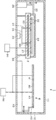
열처리 장치(1)는, 하우징(11)을 구비하고, 하우징(11)의 측벽에는 웨이퍼(W)의 반송구(12)가 마련되어 있다. 하우징(11) 내에 있어서 반송구(12)가 개구되어 있는 측을 전방측이라 하면, 하우징(11) 내의 후방측에는, 하우징(11)의 저면에 지지 기둥(23)을 통해 설치된 수평한 원형의 열판(2)이 마련되어 있다. 열판(2)의 상면에는 웨이퍼(W)를 지지하는 갭 핀(22)이 다수 분산되어 마련되어 있다. 또한 열판(2)에는, 예를 들어 발열 저항체로 이루어지는 히터(21)가 매설되어, 열판(2)에 적재된 웨이퍼(W)를, 제1 온도, 예를 들어 110℃로 가열 처리할 수 있도록 구성되어 있다. 열판(2)에는, 열판(2)을 두께 방향으로 관통하는 관통 구멍(30)이 주위 방향으로 3개소 마련되어 있다. 각 관통 구멍(30)에는 수직인 승강 핀(31)이 삽입 관통되어 있다. 각 승강 핀(31)은 승강판(32)을 통해 하우징(11)의 저면에 설치된 승강 기구(33)에 접속되고, 각 승강 핀(31)은, 승강 기구(33)에 의해 승강하여, 승강 핀(31)의 선단은 열판(2)의 표면에 있어서 돌출 함몰된다. 도 1 중의 부호 94는 히터(21)를 승온시키기 위한 전원부이다.The
열판(2)의 상방에는 열판(2)에 적재된 웨이퍼(W)를 둘러싸도록, 저면측이 개구된 편평한 원통형 커버(24)가 마련된다. 커버(24)는 지지부(25)를 통해 승강 기구(26)에 접속되고, 커버(24)는 열판(2) 상에 있어서 승강한다. 웨이퍼(W)를 가열 처리할 때는, 도 1에 도시한 바와 같이 커버(24)의 측벽의 하단은 열판(2)에 접하고, 커버(24)와 열판(2)에 의해, 웨이퍼(W)의 주위가 구획되고, 웨이퍼(W)를 열판(2)으로 전달할 때는, 커버(24)가 상승하여, 웨이퍼(W)의 주위가 개방된다.On the upper side of the
하우징(11) 내의 전방측(반송구(12)측)에는 반송체인 반송 암(4)이 마련된다. 반송 암(4)은 수평인 개략 원판형 지지부인 지지 플레이트(40)를 구비하고, 지지 플레이트(40)의 표면에 웨이퍼(W)가 적재된다. 이 지지 플레이트(40)는 지지 부재(42)를 통해 접속된 이동 기구(43)에 의해 전후 방향으로 이동하고, 열판(2)의 상방 영역과, 열판(2)의 횡방향으로 벗어난 외측 영역(도 1에 도시하는 위치) 사이에서 이동할 수 있다.On the front side (the
반송 암(4)이 외측 영역에 위치할 때, 웨이퍼(W)를 보유 지지한 열처리 장치(1)의 외부의 반송 기구가 반송구(12)로부터 하우징(11) 내로 진입하여, 지지 플레이트(40)의 상방으로부터 하방으로 승강함으로써, 당해 외부의 반송 기구와 암(34) 사이에서 웨이퍼(W)의 전달이 행해진다. 또한 이 예에서는, 외부의 반송 기구는, 웨이퍼(W)의 주연부를 등간격으로 4개소 하방측으로부터 지지하도록 구성되어 있다. 따라서 웨이퍼(W)를 전달할 때 반송 기구와 지지 플레이트(40)가 서로 간섭하는 것을 피하기 위해, 지지 플레이트(40)의 주연에는, 등간격으로 4개소의 절결부(44)가 형성되어 있다. 또한 도 2에 도시한 바와 같이, 지지 플레이트(40)에는, 후단으로부터 전방측을 향해 슬릿(45)이 형성되어 있다. 이 슬릿(45)에 의해 열판(2) 위에 지지 플레이트(40)가 위치했을 때, 열판(2)으로부터 돌출 함몰되는 승강 핀(31)이 당해 슬릿(45)을 통해 지지 플레이트(40) 위로 돌출될 수 있고, 승강 핀(31)의 승강과 반송 암(4)의 진퇴의 협동에 의해, 열판(2)과 지지 플레이트(40) 사이에서 웨이퍼(W)의 전달이 행해진다. 승강 핀(31)은, 전달 기구에 상당한다.When the
또한 지지 플레이트(40)의 내부에는, 가열 기구 및 냉각 기구를 겸용하는 펠티에 소자부(41)가 매설되어 있다. 펠티에 소자부(41)는 펠티에 소자부(41)에 공급하는 전류의 방향을 전환하고, 지지 플레이트(40)를 제2 온도, 예를 들어 40℃에서 가열하는 가열 상태와, 제3 온도, 예를 들어 23℃에서 냉각하는 냉각 상태로 전환하는 온냉 전환부(95)에 접속되어 있다. 또한 온냉 전환부(95)는, 펠티에 소자부(41)에 공급하는 전류의 크기를 조정하고, 펠티에 소자부(41)의 가열 온도 및 냉각 온도를 조정할 수 있도록 구성해도 된다. 펠티에 소자부(41)는, 예를 들어 전후 2행 좌우 2열의 2×2의 행렬형으로 4분할되어 있고, 지지 플레이트(40)에 적재된 웨이퍼(W)의 전체면을 균일하게 가열 혹은 냉각할 수 있도록 구성되어 있다. 이와 같이 열처리 장치(1)에 있어서는, 열판(2)의 상방 영역과 그 외측 영역 사이에서 웨이퍼(W)를 직접 반송하는 반송체인 반송 암(4)에 마련된 지지 플레이트(40)에 의해 웨이퍼(W)의 가열 및 냉각을 행한다. 즉, 웨이퍼(W)를 온도 조정하는 반송체와, 열판(2)의 상방 영역으로 웨이퍼(W)를 반송하는 반송체가 일체로 되어 있다.In addition, inside the
도 3에 도시한 바와 같이 열처리 장치(1)는, 예를 들어 컴퓨터로 이루어지는 제어부(9)를 구비하고 있다. 제어부(9)는, CPU(91), 메모리(92), 프로그램 저장부(93)를 구비하고 있다. 도 3 중의 부호 90은 버스이다. 또한 제어부(9)는, 온냉 전환부(95), 히터(21)를 가열하는 전원부(94), 반송 암(4)의 이동 기구(43), 각 승강 기구(33, 26)(도 3 중에서는, 커버(24)의 승강 기구는 생략한다)에 제어 신호를 출력할 수 있도록 구성되어 있다.As shown in FIG. 3, the
프로그램 저장부(93)에는, 후술하는 열처리 장치(1)의 작용에 나타내는 펠티에 소자부(41)의 가열 상태와 냉각 상태의 전환의 제어, 반송 암(4)의 이동, 커버(24)의 승강, 웨이퍼(W)의 전달 등의 시퀀스가 실시되도록 명령(스텝군)이 짜인, 프로그램이 저장된다. 이 프로그램은, 예를 들어 콤팩트 디스크, 하드 디스크, MO(광자기 디스크), DVD, 메모리 카드 등의 기억 매체에 의해 저장되어 제어부(9)에 인스톨된다.In the
계속해서 본 실시 형태에 관한 열처리 장치(1)의 작용에 대하여 도 4 내지 도 9의 모식도를 사용하여 설명한다. 화학 증폭형 레지스트막이 형성되어 노광 처리가 행해진 웨이퍼(W)는, 하우징(11)의 외부의 반송 기구 A5에 의해 하우징(11) 내로 반송된다. 열처리 장치(1)에 있어서는, 웨이퍼(W)가 반송되기 전에, 열판(2)이, 예를 들어 110℃로 가열되고, 지지 플레이트(40)는, 예를 들어 23℃로 냉각된 냉각 상태에서 외측 영역에 대기하고 있다. 도 4 내지 도 9에 있어서는, 지지 플레이트(40)가 냉각 상태(23℃)일 때는, 지지 플레이트(40)로부터 파선의 화살표를 뻗쳐 나타내고, 지지 플레이트(40)가 가열 상태일 때는, 지지 플레이트(40)로부터 실선의 파형의 화살표를 뻗쳐 나타내고 있다. 열판(2)에 적재된 웨이퍼(W)가 가열되어 있을 때도 열판(2)으로부터 실선의 파형의 화살표를 뻗쳐 나타내고 있다.Subsequently, the operation of the
먼저 도 4에 도시한 바와 같이, 열처리 장치(1) 내에 열처리 대상의 웨이퍼(W)를 보유 지지한 반송 기구 A5를 진입시켜, 지지 플레이트(40)의 상방으로부터 하방으로 이동시켜 웨이퍼(W)를 지지 플레이트(40) 위에 적재한다. 그리고, 예를 들어 도 5에 도시한 바와 같이 웨이퍼(W)가 지지 플레이트(40)에 적재되는 동시에, 펠티에 소자부(41)를 냉각 상태로부터 가열 상태로 전환한다. 이에 의해 웨이퍼(W)의 온도는 냉각 온도인 23℃로부터, 레지스트막의 내부에 있어서 산이 확산을 개시하는 온도의 하한보다도 낮은 온도, 예를 들어 40℃까지 승온된다.First, as shown in FIG. 4, the transfer mechanism A5 holding the wafer W to be subjected to heat treatment is introduced into the
이어서 도 6에 도시한 바와 같이, 열판(2)측의 커버(24)를 상승시켜, 지지 플레이트(40)를 가열 상태로 한 채, 열판(2)의 바로 위의 상방 영역으로 이동시킨다. 또한 승강 핀(31)에 의해 지지 플레이트(40)에 지지된 웨이퍼(W)를 밀어올려 수취하고, 지지 플레이트(40)를 외측 영역으로 후퇴시킨다. 그 후 도 7에 도시한 바와 같이, 승강 핀(31)을 하강시켜 열판(2)에 웨이퍼(W)를 적재하고, 커버(24)를 하강시킨다. 이에 의해 웨이퍼(W)가 열판(2)에 의해 다시 110℃로 가열되어, 웨이퍼(W)의 면 내에서 산 확산 반응이 진행된다. 지지 플레이트(40)에 있어서는, 웨이퍼(W)를 승강 핀(31)으로 전달한 후에는 펠티에 소자부(41)를 냉각 상태로 전환하고, 외측 영역에서 대기한다.Subsequently, as shown in FIG. 6, the
그리고 웨이퍼(W)의 가열이 완료되면, 승강 핀(31)에 의해 열판(2) 위의 웨이퍼(W)를 밀어올려, 지지 플레이트(40)를 냉각 상태로 한 채, 상방 영역으로 이동시킨다. 또한 도 8에 도시한 바와 같이 승강 핀(31)을 하강시켜 웨이퍼(W)를 지지 플레이트(40)로 전달한다. 지지 플레이트(40)는, 웨이퍼(W)를 수취하면 도 9에 도시한 바와 같이 빠르게 외측 영역으로 이동한다. 지지 플레이트(40)는, 미리 냉각 상태로 전환되어 있기 때문에, 지지 플레이트(40)에 적재된 직후부터 웨이퍼(W)의 냉각이 개시된다. 그리고, 지지 플레이트(40)는 웨이퍼(W)를 열판(2) 위로 반송했을 때보다도 낮은 온도이기 때문에, 적재된 웨이퍼(W)의 온도는 급격하게 저하되고, 웨이퍼(W)의 면 내 전체에서 산 확산 반응이 정지된다.Then, when the heating of the wafer W is completed, the wafer W on the
그리고 반송 암(4)이 외측 위치에 대기하고 있는 동안에 웨이퍼(W)는, 예를 들어 23℃까지 냉각된다. 그 후, 예를 들어 외부의 반송 기구 A5를 지지 플레이트(40)의 하방으로 진입시켜, 반송 기구 A5를 상승시킨다. 이에 의해 지지 플레이트(40)에 적재된 웨이퍼(W)가 반송 기구 A5로 전달된다. 이후 지지 플레이트(40)는, 냉각 상태를 유지한 채 외측 영역에서, 후속 웨이퍼(W)를 반송하기 위해 대기한다. 후속 웨이퍼(W)에 대해서도, 먼저 처리된 웨이퍼(W)와 마찬가지로 처리가 행해진다. 즉, 앞서 설명한 수순으로 처리가 행해진다.And the wafer W is cooled to 23 degreeC, for example, while the
여기서, 상기와 같이 열판(2)에 적재 전의 웨이퍼(W)를 지지 플레이트(40)에 의해 가열하는 이유에 대하여 설명한다. 열처리 장치(1)로부터 반출된 웨이퍼(W)는 현상 장치로 반송된다. 현상 장치에 있어서는, 웨이퍼(W)에 현상액을 공급하여 레지스트막에 노광된 패턴을 현상한다. 화학 증폭형 레지스트를 도포한 웨이퍼(W)에 있어서는, 노광 처리를 행한 후, 예를 들어 110℃로 가열함으로써, 레지스트 중에 산이 확산된다. 이 산에 의해 네거티브형 레지스트의 경우에는 노광되지 않은 영역이 현상액에 가용으로 되고, 포지티브형 레지스트의 경우에는 노광된 영역이 현상액에 가용으로 된다. 이때 웨이퍼(W)를 면 내에서 균일하게 가열함으로써, 레지스트막 중에 산이 균일하게 확산되어, 현상 처리를 행하였을 때의 선 폭이 균일해진다.Here, the reason for heating the wafer W before loading on the
그러나 웨이퍼(W)를 열판(2)에 둔 직후는, 당해 웨이퍼(W)의 면 내에 있어서 온도의 균일성을 제어하기 어렵고, 구체적으로는, 웨이퍼(W)의 면 내에서 승온 과도 특성(승온을 개시한 후, 온도가 일정해질 때까지의 온도 변화의 특성)에 차가 발생해 버린다. 즉, 웨이퍼(W)의 온도를 면 내에서 균일하게 유지한 채 목표 온도까지 상승시키는 것은 어렵다. 특히 열판(2)의 온도와, 웨이퍼(W)의 온도의 차가 큰 경우에는, 웨이퍼(W)의 면 내에서 승온 과도 특성에 대한 차가 발생하기 쉬워진다. 그리고 웨이퍼(W)의 면 내에서 승온 과도 특성에 차가 발생하면, 웨이퍼(W)의 면 내에 있어서 열 이력에 차가 발생해 버려, 웨이퍼(W)의 면 내에 있어서 산의 확산 상태가 변동되어, 현상 처리 시에 패턴의 선 폭의 균일성이 나빠질 우려가 있다. 근년에는 열판(2)의 히터 패턴의 최적화나 제어 등에 의해 승온 과도 특성의 향상을 도모하고 있지만 패턴의 미세화를 도모하는 면에서 가일층 개선이 요구되고 있다.However, immediately after placing the wafer W on the
그래서, 상술한 실시 형태에 의하면, 노광 후의 레지스트막이 형성된 현상 전의 웨이퍼(W)를 열처리하는 열처리 장치(1)에 있어서, 웨이퍼(W)를 레지스트막 중의 산이 확산되는 제1 온도로 가열하는 열판(2)을 마련하고 있다. 또한 열판(2)의 상방 영역과, 상방 영역으로부터 횡방향으로 벗어난 외측 영역 사이에서, 지지 플레이트(40)에 적재된 웨이퍼(W)를 반송하는 반송 암(4)을 마련하고 있다. 그리고 외측 영역에서 열판(2)에 의한 가열을 행하기 전에 지지 플레이트(40)에 적재된 웨이퍼(W)를 레지스트막 중의 산이 확산되는 온도보다도 낮은 제2 온도로 가열하도록 구성하고, 열판(2)에서 가열 처리를 행한 웨이퍼(W)를 지지 플레이트(40)에 의해 외측 영역으로 반송할 때 제2 온도보다도 낮은 제3 온도로 냉각하도록 하고 있다.Thus, according to the above-described embodiment, in the
그 때문에 열처리 장치(1)로 반입된 웨이퍼(W)를 열판(2)으로 전달하기 전에 미리 레지스트막이 반응하는 온도보다도 낮은 온도로 가열하고, 그 후 열판(2)으로 전달할 수 있다. 따라서 열판(2)에 적재한 후의 웨이퍼(W)의 제1 온도와 열판(2)에 적재되기 전의 웨이퍼(W)의 온도의 차가 작아져, 웨이퍼(W)의 면 내에 있어서, 승온 과도 특성의 차가 작아지기 때문에, 웨이퍼(W)의 면 내에서 균일성 높게 반응이 진행된다. 그리고, 그 후, 웨이퍼(W)의 제3 온도로 냉각함으로써, 면 내 전체에서 동시에 반응을 정지시킨다. 이와 같이 처리가 행해짐으로써, 웨이퍼(W)의 면 내 각 부에서 균일성 높게 레지스트막을 반응시킬 수 있다. 따라서, 당해 웨이퍼(W)를 현상했을 때 패턴의 선 폭을 균일하게 할 수 있다.Therefore, before transferring the wafer W carried into the
또한, 상기한 인용 문헌 1의 장치에서는 열판이 포함되는 용기 내에 마련되는 가열부에 의해, 열판에 적재 전의 웨이퍼(W)를 가열한다. 그 때문에, 용기 내의 온도 분포의 영향을 받게 되므로, 웨이퍼(W)의 면 내에서 정밀도 높게 온도를 제어하는 것은 어렵다고 생각된다. 따라서, 열처리 장치(1)에서는, 인용 문헌 1의 장치보다도 웨이퍼(W)의 면 내에서 균일성 높은 처리를 행할 수 있다.In addition, in the above-mentioned apparatus of Cited
그런데 상기한 열처리 장치(1)에 의한 처리에 있어서는, 열판(2)에 웨이퍼(W)를 전달한 후, 지지 플레이트(40)가 가열 상태로부터 냉각 상태로 전환되고, 열판(2)에 의한 웨이퍼(W)의 가열과, 지지 플레이트(40)의 강온이 병행하여 행해진다. 따라서, 열판(2)에 의한 처리 완료 후, 빠르게 지지 플레이트(40)에 의해 웨이퍼(W)를 냉각하여, 과잉으로 반응이 진행되는 것을 방지할 수 있다. 또한 열판(2)에 의한 처리 완료 후에 지지 플레이트(40)를 냉각하기 위해 필요한 시간을 마련할 필요가 없으므로 스루풋의 저하를 방지할 수 있다.By the way, in the process by the above-mentioned
또한, 지지 플레이트(40)를 가열 상태로부터 냉각 상태로 전환하는 타이밍으로서는, 상기한 예에는 한정되지 않고, 예를 들어 웨이퍼(W)를 승강 핀(31)으로 전달하기 직전이어도 되고, 지지 플레이트(40)가 외측 영역으로 이동한 후여도 된다.In addition, the timing for switching the
또한, 상기한 열처리 장치(1)에 의한 처리에 있어서는, 지지 플레이트(40)에 웨이퍼(W)가 적재되는 동시에 지지 플레이트(40)가 가열 상태로 되어 승온이 개시된다. 웨이퍼(W)가 급격하게 비교적 높은 온도로 되면 당해 웨이퍼(W)에 휨이 발생할 우려가 있다. 그리고, 이 휨에 의해 열처리 장치(1)에 있어서 웨이퍼(W)의 면 내 각 부의 반응에 변동이 발생할 우려가 있다. 그러나, 상기와 같이 웨이퍼(W)가 적재되는 타이밍에 지지 플레이트(40)의 가열을 개시하고 있으므로, 그와 같은 문제를 방지할 수 있다.In addition, in the process by the above-mentioned
또한, 열처리 장치(1)로 순차 반송되는 각 웨이퍼(W)에 대하여 이와 같은 타이밍에 지지 플레이트(40)에 의한 가열이 행해지므로, 웨이퍼(W) 사이에서 지지 플레이트(40)에 의한 가열이 개시되고 나서, 열판(40)으로 전달되어 지지 플레이트(40)에 의한 가열이 종료될 때까지의 시간의 길이가 맞추어지게 된다. 따라서, 상기와 같이 지지 플레이트(40)의 승온 개시의 타이밍을 제어하는 것은, 웨이퍼(W) 사이에서 균일성 높은 처리를 행하는 것이 되기도 한다. 또한, 웨이퍼(W)가 적재되는 타이밍과 지지 플레이트(40)가 가열 상태로 전환되는 타이밍이 동시라고 설명했지만, 웨이퍼(W)가 지지 플레이트(40)에 적재되고 나서 소정의 시간이 경과한 후에 지지 플레이트(40)의 가열 상태로 전환이 행해지도록 해도 된다.In addition, since heating by the
그런데, 예를 들어 선행의 웨이퍼(W)를 열처리 장치(1)로부터 반출하기 위해 지지 플레이트(40)에 의해 냉각한 후, 후속 웨이퍼(W)를 지지 플레이트(40)에 적재하기 전에 지지 플레이트(40)의 온도를 상승시켜 소정의 온도로 하고, 당해 소정의 온도로 된 지지 플레이트(40)에 후속 웨이퍼(W)를 적재하여 가열하는 것도 생각된다. 즉, 상기와 같이 복수의 웨이퍼(W)를 열처리 장치(1)로 순차 반송하여 처리함에 있어서, 각 웨이퍼(W)를 지지 플레이트(40)로 반송하기 전에, 지지 플레이트(40)가 소정의 온도로 되도록 가열해 두어도 된다. 단, 그 경우, 반송 기구 A5에 의한 각 웨이퍼(W)의 반송 상황에 따라서는, 열처리 장치(1)로의 웨이퍼(W)의 반송 시에 지지 플레이트(40)가 소정의 온도에 도달되지 않아, 당해 반송 기구 A5가 웨이퍼(W)를 지지 플레이트(40)로 전달되지 못하고 대기시킬 필요가 발생하는 것이 생각된다. 따라서, 그와 같은 대기 시간이 발생하는 것을 방지하여 스루풋을 향상시키기 위해, 지지 플레이트(40)의 냉각 상태로부터 가열 상태의 전환은, 이미 설명한 바와 같이 지지 플레이트(40)로의 웨이퍼(W)의 적재 후 혹은 적재와 동시에 행하는 것이 바람직하다.By the way, for example, after cooling by the
또한, 웨이퍼(W)의 면 내 및 복수의 웨이퍼(W) 사이에서 균일한 처리를 행하기 위해서는, 지지 플레이트(40)에 의해 가열된 웨이퍼(W)의 온도가 상기한 제2 온도에서 안정된 상태로 웨이퍼(W)를 오븐으로 반입하는(열판(2)의 상방 영역에 위치시키는) 것이 바람직하다. 즉, 웨이퍼(W)의 온도가 제2 온도에 도달하고 나서, 오븐으로 반입될 때까지 충분한 시간을 확보하는 것이 바람직하다. 단, 웨이퍼(W)가 지지 플레이트(40)에 적재되고 나서 오븐으로 반입될 때까지의 시간이 너무 길면, 스루풋의 저하를 초래하여, 레지스트막이 변질될 우려가 있다. 그래서, 오븐으로 웨이퍼(W)를 반입할 예정 타이밍에 따라, 웨이퍼(W)를 적재한 지지 플레이트(40)의 냉각 상태로부터 가열 상태로의 전환의 타이밍을 조정하도록 제어를 행하는 것이 바람직하다. 바꾸어 말하면, 오븐으로 웨이퍼(W)가 반입되는 타이밍과 지지 플레이트(40)에 의한 가열이 개시되는 타이밍의 시간이 소정의 시간으로 되도록 제어하는 것이 바람직하다.In addition, in order to perform uniform processing between the surfaces of the wafer W and the plurality of wafers W, the temperature of the wafer W heated by the
이와 같은 제어의 구체적인 일례를 설명한다. 예를 들어, 열판(2)의 온도의 변경 중에는 웨이퍼(W)를 오븐으로 반입할 수 없다고 하자. 지지 플레이트(40)에 웨이퍼(W)가 적재되었을 때, 상기한 일련의 동작에 의해 지지 플레이트(40)가 상방 영역에 위치할 예정 타이밍이 오븐으로 웨이퍼(W)를 반입할 수 없는 기간과 겹치는 경우, 그 반입할 수 없는 기간의 종료 후에 지지 플레이트(40)가 상방 영역에 위치하도록 가열 상태의 전환의 타이밍을 지연시킨다. 즉, 웨이퍼(W)를 지지 플레이트(40)에 적재하는 동시에 지지 플레이트(40)에 의한 가열을 행하는 것이 아니라, 지지 플레이트(40)에 대기시킨 후에 당해 가열을 개시하고, 이 가열 개시부터 오븐 반입까지의 시간이 예정된 시간으로부터 어긋나지 않도록 한다.A specific example of such control will be described. For example, suppose that the wafer W cannot be brought into the oven while the temperature of the
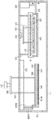
열처리 장치(1)는, 웨이퍼(W)를 가열하여 열판(2)으로 전달하는 반송 암(4)과, 열판(2)에서 가열한 웨이퍼(W)를 수취하여 냉각하는 반송 암(4)을 각각 개별로 구비하고 있어도 된다. 예를 들어, 도 1, 도 2에 도시한 열처리 장치(1)의 반송 암(4) 대신에, 도 10에 도시한 바와 같이 열판(2)의 전방측에, 가열 암(4A)과, 냉각 암(4B)을 상하로 적층하여 마련한다. 가열 암(4A)과, 냉각 암(4B)은, 각각 지지 플레이트(400)를 구비하고, 가열 암(4A)의 지지 플레이트(40)에는, 히터(41A)를 매설하고, 냉각 암(4B)에는, 예를 들어 냉각수를 통류할 수 있도록 구성한 수랭관(41B)을 매설하면 된다.The
또한 각각 개별로 외측 영역과 열판(2)의 상방 영역 사이를 이동할 수 있도록 구성하면 된다. 도 10 중 부호 42A, 42B는 각각 가열 암(4A), 냉각 암(4B)의 지지 플레이트(40)를 지지하는 지지부이고, 부호 43은 가열 암(4A), 냉각 암(4B)을 개별로 이동시키는 이동 기구이다. 또한 도 10의 예에서는, 승강 핀(31)과 마찬가지로 구성된 승강 핀(34)을 마련하여, 승강 핀(34)을 승강판(35)을 통해 승강 기구(36)에 접속하고 있다. 그리고 승강 핀(34)과, 외부의 반송 기구의 협동 작용에 의해 전달을 행하도록 구성하고 있다.In addition, each may be configured to be able to individually move between the outer region and the upper region of the
그리고 가열 처리 전의 웨이퍼(W)를 23℃의 온도로 한 가열 암(4A)에 적재하고, 그 후 23℃로부터 40℃로 승온된다. 또한 가열 암(4A)을 상방 영역으로 이동시켜 웨이퍼(W)를 열판(2)으로 전달한다. 또한 가열 처리 후의 웨이퍼(W)를 냉각 암(4B)에서 수취하여, 23℃로 냉각한다. 또한 냉각 암(4B)으로부터 외부의 반송 기구로 웨이퍼(W)를 전달하는 데 있어서는, 가열 암(4A)을 열판(2)의 상방 영역으로 이동시켜 냉각 암(4B)에 적재된 웨이퍼(W)를 승강 핀(34)으로 밀어올려, 외부의 반송 기구로 전달하도록 하면 된다. 또한 이와 같이 웨이퍼(W)를 가열하여 반송하는 가열 암(4A)과, 웨이퍼(W)를 냉각하여 반송하는 냉각 암(4B)을 상하로 배치함으로써, 열처리 장치(1) 내에 복수의 반송 암(4)을 마련한 경우에도, 장치의 점유 면적의 대형화를 피할 수 있는 효과가 있다. 나아가 도 1, 도 2와 같이 1대의 반송 암(4)에 의해 웨이퍼(W)의 가열 상태와, 냉각 상태를 전환할 수 있도록 구성함으로써 웨이퍼(W)를 제2 온도로 가열하는 반송 암(4)과, 제3 온도로 냉각하는 반송 암(4)을 개별로 마련할 필요가 없어 장치의 대형화를 억제할 수 있는 효과가 있다.Then, the wafer W before the heat treatment is placed on the
또한 지지 플레이트(40) 내에, 온도 조절수의 배관 및 냉각수의 배관, 혹은 히터 및 냉각 기구를 매설해도 된다. 도 1, 도 2에 도시한 열처리 장치(1)에 있어서는, 지지 플레이트(40)에 공급되는 전류의 방향에 의해 가열과 냉각을 전환할 수 있는 펠티에 소자부(41)를 마련하고 있다. 그 때문에 웨이퍼(W)를 제2 온도로 가열하는 가열 기구와, 제3 온도로 냉각하는 냉각 기구를 개별로 마련할 필요가 없어 장치의 대형화나 레이아웃의 복잡화를 피할 수 있다.In addition, a pipe of temperature-adjusted water and a pipe of cooling water, or a heater and a cooling mechanism may be embedded in the
또한 노광 후의 레지스트막을 열판(2)에 적재하여 가열할 때의 가열 온도는, 110℃ 정도인 점에서, 지지 플레이트(40)에서 웨이퍼(W)를 가열할 때는, 분위기의 온도보다도 높은 제2 온도, 예를 들어 20℃ 내지 70℃로 가열하도록 하면 된다. 일반적으로, 열판(2)에 의한 가열 온도는 레지스트종마다의 권장 처리 온도로부터 결정되지만, 엄밀하게는 레지스트막은 그것보다도 낮은 온도로부터 적지 않게 반응은 개시된다. 환언하면, 레지스트막의 반응 개시 온도는, 열판(2)에 의한 가열 온도보다도 낮다. 즉, 제2 온도는, 적어도 상온(장치 내 분위기 온도)보다 높고 레지스트막의 반응 개시 온도 이하여야 하며, 금회와 같이 열판(2)에 의한 가열 온도에 비해 20% 이상 낮게 설정되는 경우가 있다.In addition, since the heating temperature when heating the resist film after exposure on the
또한 웨이퍼(W)를 열판(2)에 적재하여 가열 처리를 행하고 있는 동안에 지지 플레이트(40)를 제3 온도, 예를 들어 23℃의 냉각 상태로 전환하여 강온해 두는 것이 바람직하다. 이와 같이 구성함으로써 열판(2)에서 가열한 웨이퍼(W)를 지지 플레이트(40)로 전달한 직후부터 빠르게 냉각할 수 있다.In addition, it is preferable to load the wafer W on the
또한 가열 처리 후의 웨이퍼(W)를 반송 암(4)으로 전달하여 제2 온도보다 낮은, 제3 온도로 냉각하지만, 이 제3 온도란, 웨이퍼(W)를 반송 암(4)에 계속해서 적재했을 때 최종적으로 도달하는 온도이고, 이 온도가 제2 온도보다도 낮으면 된다. 따라서 가열 처리 후의 웨이퍼(W)를 반송 암(4)으로 전달한 후, 웨이퍼(W)의 온도가 제2 온도 이하로 미처 내려가지 못한 동안에, 웨이퍼(W)를 열처리 장치(1)의 외부로 전달하는 구성이라도 본 개시의 범위에 포함된다.In addition, the wafer W after the heat treatment is transferred to the
또한 웨이퍼(W)를 열처리 장치(1)로 반송하기 전에 웨이퍼(W)의 온도 측정을 행하고, 측정 온도에 기초하여, 외부로부터 웨이퍼(W)를 수취할 때 지지 플레이트(40)의 온도를 조정하도록 해도 된다. 예를 들어, 도 11에 도시한 바와 같이 외부의 반송 기구 A5에 보유 지지된 웨이퍼(W)의 온도를 측정하는 온도 측정부(96)를 당해 반송 기구 A5에 마련하고, 당해 온도 측정부(96)는 측정 온도에 상당하는 측정 신호를 제어부(9)에 출력하도록 구성된다. 그리고 제어부(9)에서, 측정 신호에 기초하여 펠티에 소자부(41)에 입력하는 전류를 조정하면 된다. 일례로서는, 검출되는 웨이퍼(W)의 측정 온도가, 어느 기준보다 낮아진 경우는 더 큰 온도 변화량이 필요하므로 지지 플레이트의 초기 온도를 높이거나 가열 시에 조금씩 온도를 높이는 방법이 취해진다. 그러나, 기판 온도가 소정 온도를 초과하는 오버슈트가 일어나지 않도록, 그렇게 하여 높아진 지지 플레이트의 온도를 가열 후반에 낮추는 방법이 생각된다. 반대로, 웨이퍼(W)의 측정 온도가, 어느 기준보다 높아진 경우는, 가열 전반의 가열 레이트를 유지하기 위해, 상기와 마찬가지로 초기 온도나 가열 시 온도 변화를 바꾸는 방법이 생각되지만, 오버슈트의 리스크와 그 가열 후반에 있어서의 대책도 마찬가지라고 할 수 있다.In addition, the temperature of the wafer W is measured before transferring the wafer W to the
또한 웨이퍼(W)를 지지 플레이트(40)에 적재하고, 제2 온도로 승온할 때 지지 플레이트(40) 상의 웨이퍼(W)의 주위의 공간을 주변으로부터 격리하는 커버를 마련해도 된다. 이와 같이 구성함으로써 웨이퍼(W)의 주위의 공간을 격리 단열할 수 있기 때문에 웨이퍼(W)의 승온을 촉진시킬 수 있는 효과가 있다. 이 커버는, 웨이퍼(W)를 냉각할 때는 상승시켜 두도록 해도 된다. 커버는, 열판(2)측의 커버(24)와 일체로 되어 승강하도록 구성해도 되고, 이때 지지 플레이트측의 커버와, 커버(24)의 연결 부분에, 예를 들어 세라믹판 등의 단열재를 끼워도 된다.Further, the wafer W may be mounted on the
계속해서 상술한 열처리 장치(1)가 내장되는 도포, 현상 장치의 전체 구성에 대하여 간단하게 설명해 둔다. 도포, 현상 장치는 도 12 및 도 13에 도시한 바와 같이 캐리어 블록 B1과, 처리 블록 B2와, 인터페이스 블록 B3을 직선형으로 접속하여 구성되어 있다. 인터페이스 블록 B3에는, 노광 스테이션 B4가 더 접속되어 있다.Subsequently, the entire configuration of the coating and developing device in which the above-described
캐리어 블록 B1은, 제품용 기판인, 예를 들어 직경 300㎜의 웨이퍼(W)를 복수매 수납하는 반송 용기인 캐리어 C(예를 들어, FOUP)로부터 장치 내로 반출입하는 역할을 갖고, 캐리어 C의 적재 스테이지(101)와, 도어(102)와, 캐리어 C로부터 웨이퍼(W)를 반송하기 위한 반송 암(103)을 구비하고 있다.The carrier block B1 serves to carry in and out the carrier C (for example, FOUP), which is a transport container for storing a plurality of wafers W having a diameter of 300 mm, which is a substrate for a product, for example, into the apparatus. A
처리 블록 B2는 웨이퍼(W)에 액 처리를 행하기 위한 제1 내지 제6 단위 블록 D1 내지 D6이 아래부터 차례로 적층되어 구성되고, 각 단위 블록 D1 내지 D6은, 후술하는 액 처리 유닛(110)에서, 웨이퍼(W)로 공급하는 처리액이 상이한 것을 제외하고 대략 동일한 구성이다.The processing block B2 is configured by stacking first to sixth unit blocks D1 to D6 sequentially for performing liquid processing on the wafer W, and each unit block D1 to D6 is a
도 13에 대표하여 단위 블록 D5의 구성을 도시하면, 단위 블록 D5에는, 캐리어 블록 B1측으로부터 인터페이스 블록 B3을 향하는 직선형 반송 영역 R3을 이동하는 반송 기구 A5와, 컵 모듈(111)을 구비한, 예를 들어 웨이퍼(W)에 현상액을 공급하기 위한 액 처리 유닛(110)이 마련되어 있다. 또한 단위 블록 D1(D2)은 액 처리 유닛(110)에 있어서 웨이퍼(W)에 반사 방지막으로 되는 처리액을 도포하고, 단위 블록 D3(D4)에 있어서는, 액 처리 유닛(110)에 있어서 웨이퍼(W)에 레지스트액을 도포한다. 또한 선반 유닛 U1 내지 U6에는 이미 설명한 열처리 장치(1)가 적층되어 있다. 반송 영역 R5의 캐리어 블록 B1측에는, 서로 적층된 복수의 모듈에 의해 구성되어 있는 선반 유닛 U7이 마련되어 있다. 반송 암(103)과 반송 기구 A5 사이의 웨이퍼(W)의 전달은, 선반 유닛 U7의 전달 모듈과 반송 암(104)을 통해 행해진다.13, the configuration of the unit block D5 is shown, and the unit block D5 is provided with a transport mechanism A5 and a
인터페이스 블록 B3은, 처리 블록 B2와 노광 스테이션 B4 사이에서 웨이퍼(W)의 전달을 행하기 위한 것이고 복수의 처리 모듈이 서로 적층된 선반 유닛 U8, U9, U10을 구비하고 있다. 또한 도면 중 부호 105, 106은 각각 선반 유닛 U8, U9 사이, 선반 유닛 U9, U10 사이에서 웨이퍼(W)의 전달을 하기 위한 반송 암이고, 도면 중 부호 107은 선반 유닛 U10과 노광 스테이션 B4 사이에서 웨이퍼(W)의 전달을 하기 위한 반송 암이다.The interface block B3 is for transferring the wafer W between the processing block B2 and the exposure station B4, and includes a shelf unit U8, U9, U10 in which a plurality of processing modules are stacked on each other. In addition,
도포, 현상 장치 및 노광 스테이션 B4로 이루어지는 시스템의 웨이퍼(W)의 반송 경로의 개략에 대하여 간단하게 설명한다. 웨이퍼(W)는 캐리어 C→반송 암(103)→ 선반 유닛 U7의 전달 모듈→ 반송 암(104)→ 선반 유닛 U7의 전달 모듈→ 단위 블록 D1(D2)→단위 블록 D3(D4)→인터페이스 블록 B3→노광 스테이션 B4의 순으로 이동해 간다. 이에 의해 웨이퍼(W)의 표면에 반사 방지막 및 레지스트막이 도포되고, 또한 레지스트막의 표면에 노광 처리가 행해진다. 또한 노광 처리가 행해진 웨이퍼(W)는 인터페이스 블록 B3을 통해, 단위 블록 D5(D6)로 반송된다.The outline of the conveyance path of the wafer W of the system comprising the coating, developing apparatus and exposure station B4 will be briefly described. The wafer W is the carrier C→the
또한 단위 블록 D5(D6)에 있어서 열처리 장치(1)로 반송되어 이미 설명한 열처리가 행해지고, 이어서 액 처리 유닛(110)으로 반송되어 현상 처리가 행해진다. 그 후 웨이퍼(W)는, 선반 유닛 U7의 전달 모듈 TRS→반송 암(103)→ 캐리어 C의 순으로 이동해 간다.Further, in the unit block D5 (D6), it is conveyed to the
이미 설명한 바와 같이 노광 후의 웨이퍼(W)는, 웨이퍼(W)를 균일하게 열처리할 것이 요구된다. 그 때문에 본 실시 형태의 열처리 장치(1)를 노광 후의 웨이퍼(W)를 가열하는 열처리 장치(1)에 적용함으로써 큰 효과를 얻을 수 있다.As already explained, the wafer W after exposure is required to heat-treat the wafer W uniformly. Therefore, a great effect can be obtained by applying the
또한 본 실시 형태에 관한 열처리 장치(1)는, 웨이퍼(W)의 노광 처리 후에 가열하는 열처리 장치 이외, 예를 들어 레지스트막을 도포한 웨이퍼(W)를 노광 스테이션 B4로 반송하기 전에 가열하는 열처리 장치(1)에 적용해도 된다. 즉, PAB(프리 어플라이드 베이크)를 행하기 위해 사용해도 된다. 단, 상기한 PEB에 대해서는, 온도의 오차에 대한 레지스트막 반응의 변화량이 크고, 웨이퍼(W)의 면 내에 있어서의 고정밀도의 온도 제어가 요구되는 점에서, 열처리 장치(1)로서는 PEB에 사용하는 것이 특히 바람직하다.In addition, the
또한, 열처리 장치(1)로서는 화학 증폭형 레지스트막의 가열 이외의 처리에 적용해도 된다. 즉, 화학 증폭형 레지스트 이외의 레지스트막이 형성된 웨이퍼(W)의 가열 처리에 사용해도 되고, 반사 방지막 형성용 약액이나 절연막 형성용 약액이 도포된 웨이퍼(W)를 가열하여, 이들 반사 방지막 및 절연막을 형성하는 경우에도 적용해도 된다. 또한, 열처리 장치(1)로서는 상기한 구성에 한정되지 않는다. 커버(24)가 마련되지 않고, 열판(2)의 일단측, 타단측에 가스 공급부, 배기부를 마련하여, 열판(2)의 일단측으로부터 타단측을 향하는 기류를 형성하여 웨이퍼(W)를 가열하는 구성이어도 된다.In addition, as the
이상에 검토한 바와 같이, 금회 개시된 실시 형태는 모든 점에서 예시이며 제한적인 것은 아니라고 생각되어야 한다. 상기한 실시 형태는, 첨부의 청구범위 및 그 주지를 일탈하지 않고, 다양한 형태로 생략, 치환, 변경되어도 된다.As reviewed above, it should be thought that the embodiment disclosed this time is an illustration and restrictive at no points. The above-described embodiment may be omitted, substituted, or changed in various forms without departing from the scope of the appended claims.
Claims (11)
상기 기판을 지지하는 지지부를 구비하고, 상기 열판의 상방 영역과 당해 상방 영역으로부터 횡방향으로 벗어난 외측 영역 사이에서 당해 기판을 반송하는 반송체와,
상기 상방 영역에 있어서의 상기 반송체와 상기 열판 사이에서 상기 기판을 전달하는 전달 기구와,
상기 외측 영역에 있어서 상기 지지부에 지지된 상기 열판에 의한 가열 전의 기판을, 상기 제1 온도보다도 낮은 제2 온도로 가열하는 가열 기구와,
상기 열판에서 가열 완료되어 상기 외측 영역으로 반송하기 위해 상기 지지부에 지지된 상기 기판이 상기 제2 온도보다도 낮은 제3 온도로 되도록 냉각하는 냉각 기구와,
제어 신호를 출력하는 제어부
를 구비하는, 열처리 장치.A hot plate for heating the loaded substrate to a first temperature,
A carrier body having a support portion for supporting the substrate, and transporting the substrate between an upper region of the hot plate and an outer region transversely deviated from the upper region;
A transfer mechanism for transferring the substrate between the carrier and the hot plate in the upper region,
A heating mechanism for heating the substrate before heating by the hot plate supported on the support in the outer region to a second temperature lower than the first temperature,
A cooling mechanism that cools the substrate supported on the support portion to a third temperature lower than the second temperature to be heated in the hot plate and transferred to the outer region;
Control unit for outputting control signals
It comprises, a heat treatment apparatus.
상기 가열 기구 및 상기 냉각 기구는, 지지된 상기 기판이 상기 제2 온도로 되도록 상기 지지부를 가열하는 가열 상태와, 지지된 상기 기판이 상기 제3 온도로 되도록 상기 지지부를 냉각하는 냉각 상태를 서로 전환하는, 열처리 장치.The method of claim 1, wherein the support is shared with the heating mechanism and the cooling mechanism,
The heating mechanism and the cooling mechanism switch between a heating state in which the support is heated so that the supported substrate is at the second temperature, and a cooling state in which the support is cooled so that the supported substrate is at the third temperature. The heat treatment device.
상기 가열 기구 및 냉각 기구는 당해 펠티에 소자에 공급하는 전류의 방향을 전환함으로써 상기 가열 상태와 상기 냉각 상태를 서로 전환하는 전환 기구에 의해 구성되는, 열처리 장치.The method according to claim 3, wherein the support is constituted by a Peltier element,
The said heating mechanism and the cooling mechanism are comprised by the switching mechanism which switches the said heating state and the said cooling state to each other by switching the direction of the electric current supplied to the said Peltier element.
상기 기판이 상기 지지부에 지지됨과 동시이거나 지지된 후에, 당해 기판을 상기 제2 온도로 하기 위해 상기 냉각 상태로부터 상기 가열 상태로의 전환이 행해지도록 상기 제어 신호가 출력되는, 열처리 장치.According to claim 3,
After the substrate is supported at the same time as or supported by the support, the control signal is output so that a switch from the cooling state to the heating state is performed to bring the substrate to the second temperature.
상기 냉각 상태로부터 상기 가열 상태로 전환되는 타이밍은, 상기 기판을 지지하는 상기 반송체가 상기 상방 영역에 위치하는 예정 타이밍에 따른 타이밍으로 되도록 상기 제어 신호가 출력되는, 열처리 장치.According to claim 3,
The timing of switching from the cooling state to the heating state is such that the control signal is output such that the carrier body supporting the substrate is at a timing according to a predetermined timing at which the upper region is located.
당해 제어부는, 상기 지지부에 적재되기 전의 상기 기판의 온도에 대한 정보를 취득하고,
상기 기판이 반송될 때의 상기 지지부의 온도가, 당해 기판의 온도에 대응하는 온도로 되도록 제어 신호를 출력하는, 열처리 장치.According to claim 3,
The control unit acquires information about the temperature of the substrate before being loaded on the support,
A heat treatment apparatus that outputs a control signal so that the temperature of the support portion when the substrate is conveyed becomes a temperature corresponding to the temperature of the substrate.
상기 기판이 상기 열판에 적재되어 있는 동안, 상기 지지부가 상기 냉각 상태로 되어 강온되도록 제어 신호를 출력하는, 열처리 장치.The method according to any one of claims 3 to 7,
While the substrate is loaded on the hot plate, a heat treatment apparatus for outputting a control signal so that the support portion is cooled to the cooling state.
각각 상기 지지부를 구비한 서로 별체의 제1 반송체와, 제2 반송체를 구비하고,
상기 가열 기구, 상기 냉각 기구에 의해 상기 제1 반송체의 지지부의 온도, 상기 제2 반송체의 온도가 각각 조정되는, 열처리 장치.The carrier according to claim 1 or 2,
Each having a first carrier and a second carrier separate from each other having the support,
The heat treatment apparatus in which the temperature of the support part of the said 1st conveyance body and the temperature of the said 2nd conveyance body are respectively adjusted by the said heating mechanism and the said cooling mechanism.
상기 기판을 지지하는 지지부를 구비하고, 상기 열판의 상방 영역과 당해 상방 영역으로부터 횡방향으로 벗어난 외측 영역 사이에서 당해 기판을 반송하는 공정과,
상기 상방 영역에 있어서의 상기 반송체와 상기 열판 사이에서 상기 기판을 전달하는 공정과,
상기 외측 영역에 있어서 상기 지지부에 지지된 상기 열판에 의한 가열 전의 기판을, 상기 제1 온도보다도 낮은 제2 온도로 가열하는 공정과,
상기 열판에서 가열 완료되어 상기 외측 영역으로 반송하기 위해 상기 지지부에 지지된 상기 기판이 상기 제2 온도보다도 낮은 제3 온도로 되도록 냉각하는 공정을 포함하는, 열처리 방법.Heating the substrate loaded on the hot plate to a first temperature;
A step of conveying the substrate between an upper region of the hot plate and an outer region transversely deviated from the upper region, having a support portion supporting the substrate;
A step of transferring the substrate between the carrier and the hot plate in the upper region;
A step of heating the substrate before heating by the hot plate supported on the support in the outer region to a second temperature lower than the first temperature;
And heating the substrate so that the substrate supported on the support portion is heated to a third temperature lower than the second temperature to be transferred to the outer region by heating in the hot plate.
Applications Claiming Priority (2)
| Application Number | Priority Date | Filing Date | Title |
|---|---|---|---|
| JPJP-P-2018-228381 | 2018-12-05 | ||
| JP2018228381A JP7200638B2 (en) | 2018-12-05 | 2018-12-05 | Heat treatment apparatus and heat treatment method |
Publications (1)
| Publication Number | Publication Date |
|---|---|
| KR20200068576A true KR20200068576A (en) | 2020-06-15 |
Family
ID=71000039
Family Applications (1)
| Application Number | Title | Priority Date | Filing Date |
|---|---|---|---|
| KR1020190151055A KR20200068576A (en) | 2018-12-05 | 2019-11-22 | Heat treatment apparatus and heat treatment method |
Country Status (4)
| Country | Link |
|---|---|
| JP (1) | JP7200638B2 (en) |
| KR (1) | KR20200068576A (en) |
| CN (1) | CN111276396A (en) |
| TW (1) | TWI830816B (en) |
Families Citing this family (1)
| Publication number | Priority date | Publication date | Assignee | Title |
|---|---|---|---|---|
| CN115376978B (en) * | 2022-07-05 | 2023-11-24 | 南京原磊纳米材料有限公司 | Multi-piece type wafer transmission cooling mechanism |
Citations (1)
| Publication number | Priority date | Publication date | Assignee | Title |
|---|---|---|---|---|
| JP2005150696A (en) | 2003-10-22 | 2005-06-09 | Tokyo Electron Ltd | Heat treatment apparatus and method therefor |
Family Cites Families (8)
| Publication number | Priority date | Publication date | Assignee | Title |
|---|---|---|---|---|
| JP3525022B2 (en) * | 1996-12-20 | 2004-05-10 | 大日本スクリーン製造株式会社 | Substrate heating device |
| JP4148388B2 (en) * | 2001-07-24 | 2008-09-10 | 東京エレクトロン株式会社 | Heat treatment equipment |
| JP2008153369A (en) * | 2006-12-15 | 2008-07-03 | Chugai Ro Co Ltd | Resist agent coater |
| JP5064069B2 (en) * | 2007-03-20 | 2012-10-31 | 株式会社Sokudo | Substrate transfer apparatus and heat treatment apparatus |
| JP5220517B2 (en) * | 2008-08-27 | 2013-06-26 | 株式会社Sokudo | Substrate processing equipment |
| JP2014022497A (en) * | 2012-07-17 | 2014-02-03 | Tokyo Electron Ltd | Thermal treatment device, thermal treatment method, program, and computer storage medium |
| JP6792368B2 (en) * | 2016-07-25 | 2020-11-25 | 株式会社Screenホールディングス | Heat treatment equipment, substrate processing equipment and heat treatment method |
| JP2018133513A (en) * | 2017-02-17 | 2018-08-23 | 株式会社Screenホールディングス | Thermal treatment device |
-
2018
- 2018-12-05 JP JP2018228381A patent/JP7200638B2/en active Active
-
2019
- 2019-11-21 TW TW108142248A patent/TWI830816B/en active
- 2019-11-22 KR KR1020190151055A patent/KR20200068576A/en active Search and Examination
- 2019-11-28 CN CN201911193354.1A patent/CN111276396A/en active Pending
Patent Citations (1)
| Publication number | Priority date | Publication date | Assignee | Title |
|---|---|---|---|---|
| JP2005150696A (en) | 2003-10-22 | 2005-06-09 | Tokyo Electron Ltd | Heat treatment apparatus and method therefor |
Also Published As
| Publication number | Publication date |
|---|---|
| CN111276396A (en) | 2020-06-12 |
| TW202101531A (en) | 2021-01-01 |
| JP2020092165A (en) | 2020-06-11 |
| JP7200638B2 (en) | 2023-01-10 |
| TWI830816B (en) | 2024-02-01 |
Similar Documents
| Publication | Publication Date | Title |
|---|---|---|
| KR100567521B1 (en) | Heat and cooling treatment apparatus and substrate processing system | |
| KR102503838B1 (en) | Substrate heating device | |
| JP5151383B2 (en) | Coating and developing apparatus, method and storage medium | |
| US7151239B2 (en) | Heat treating apparatus and heat treating method | |
| KR101314001B1 (en) | Temperature control method, temperature controller, and heat treatment apparatus | |
| JPH07297258A (en) | Carrying equipment of plate body | |
| KR20070122390A (en) | Substrate treatment method and apparatus | |
| JP5296022B2 (en) | Heat treatment method, recording medium recording program for executing heat treatment method, and heat treatment apparatus | |
| KR101999890B1 (en) | Thermal processing device, substrate processing apparatus and thermal processing method | |
| KR101667434B1 (en) | Heat treatment apparatus, heat treatment method and recording medium | |
| KR20170050061A (en) | Substrate treating apparatus | |
| JP2001143850A (en) | Substrate heat treatment apparatus, substrate heat treatment method, substrate processing apparatus and substrate processing method | |
| TWI381422B (en) | A temperature control method, a program, a computer recording medium, and a substrate processing system for a heating device for a substrate processing system | |
| JP4811860B2 (en) | Heat treatment method, program thereof, and heat treatment apparatus | |
| KR20200068576A (en) | Heat treatment apparatus and heat treatment method | |
| JP2001077014A (en) | Substrate transfer device and sustem for coating- development process | |
| JP2007214367A (en) | Heat treatment apparatus, heat treatment method and program | |
| KR20030087942A (en) | Processing method and processing apparatus | |
| JP3525022B2 (en) | Substrate heating device | |
| KR20130135110A (en) | Heat processing apparatus, cooling method for heat processing plate, and computer storage medium | |
| JP2014022497A (en) | Thermal treatment device, thermal treatment method, program, and computer storage medium | |
| JP3451166B2 (en) | Substrate heat treatment equipment | |
| JP2000091218A (en) | Heating method and apparatus | |
| JP4053728B2 (en) | Heating / cooling processing apparatus and substrate processing apparatus | |
| KR102516013B1 (en) | Substrate heating apparatus and substrate heating method |
Legal Events
| Date | Code | Title | Description |
|---|---|---|---|
| A201 | Request for examination |