KR20200046130A - Light-emitting element - Google Patents
Light-emitting element Download PDFInfo
- Publication number
- KR20200046130A KR20200046130A KR1020207011838A KR20207011838A KR20200046130A KR 20200046130 A KR20200046130 A KR 20200046130A KR 1020207011838 A KR1020207011838 A KR 1020207011838A KR 20207011838 A KR20207011838 A KR 20207011838A KR 20200046130 A KR20200046130 A KR 20200046130A
- Authority
- KR
- South Korea
- Prior art keywords
- light emitting
- emitting element
- compound
- emission spectrum
- excitation
- Prior art date
Links
- 0 CCCC[C@](C1)(C1(C)c(cccc1)c1-c1c2)*1c*c2-c1ccccc1 Chemical compound CCCC[C@](C1)(C1(C)c(cccc1)c1-c1c2)*1c*c2-c1ccccc1 0.000 description 2
- FEYJCWNQZBKYKT-UHFFFAOYSA-N Clc1cnc(c2ccccc2c2ccccc22)c2n1 Chemical compound Clc1cnc(c2ccccc2c2ccccc22)c2n1 FEYJCWNQZBKYKT-UHFFFAOYSA-N 0.000 description 1
- MKAQNAJLIITRHR-UHFFFAOYSA-N c(cc1c2ccc3)ccc1[s]c2c3-c1cccc(-c2cnc(c3ccccc3c3ccccc33)c3n2)c1 Chemical compound c(cc1c2ccc3)ccc1[s]c2c3-c1cccc(-c2cnc(c3ccccc3c3ccccc33)c3n2)c1 MKAQNAJLIITRHR-UHFFFAOYSA-N 0.000 description 1
Images


Classifications
-
- H—ELECTRICITY
- H10—SEMICONDUCTOR DEVICES; ELECTRIC SOLID-STATE DEVICES NOT OTHERWISE PROVIDED FOR
- H10K—ORGANIC ELECTRIC SOLID-STATE DEVICES
- H10K85/00—Organic materials used in the body or electrodes of devices covered by this subclass
- H10K85/60—Organic compounds having low molecular weight
- H10K85/631—Amine compounds having at least two aryl rest on at least one amine-nitrogen atom, e.g. triphenylamine
-
- H01L51/0059—
-
- H—ELECTRICITY
- H10—SEMICONDUCTOR DEVICES; ELECTRIC SOLID-STATE DEVICES NOT OTHERWISE PROVIDED FOR
- H10K—ORGANIC ELECTRIC SOLID-STATE DEVICES
- H10K85/00—Organic materials used in the body or electrodes of devices covered by this subclass
- H10K85/30—Coordination compounds
- H10K85/341—Transition metal complexes, e.g. Ru(II)polypyridine complexes
- H10K85/342—Transition metal complexes, e.g. Ru(II)polypyridine complexes comprising iridium
-
- C—CHEMISTRY; METALLURGY
- C07—ORGANIC CHEMISTRY
- C07D—HETEROCYCLIC COMPOUNDS
- C07D209/00—Heterocyclic compounds containing five-membered rings, condensed with other rings, with one nitrogen atom as the only ring hetero atom
- C07D209/56—Ring systems containing three or more rings
- C07D209/80—[b, c]- or [b, d]-condensed
- C07D209/82—Carbazoles; Hydrogenated carbazoles
- C07D209/86—Carbazoles; Hydrogenated carbazoles with only hydrogen atoms, hydrocarbon or substituted hydrocarbon radicals, directly attached to carbon atoms of the ring system
-
- C—CHEMISTRY; METALLURGY
- C07—ORGANIC CHEMISTRY
- C07D—HETEROCYCLIC COMPOUNDS
- C07D239/00—Heterocyclic compounds containing 1,3-diazine or hydrogenated 1,3-diazine rings
- C07D239/02—Heterocyclic compounds containing 1,3-diazine or hydrogenated 1,3-diazine rings not condensed with other rings
- C07D239/24—Heterocyclic compounds containing 1,3-diazine or hydrogenated 1,3-diazine rings not condensed with other rings having three or more double bonds between ring members or between ring members and non-ring members
- C07D239/26—Heterocyclic compounds containing 1,3-diazine or hydrogenated 1,3-diazine rings not condensed with other rings having three or more double bonds between ring members or between ring members and non-ring members with only hydrogen atoms, hydrocarbon or substituted hydrocarbon radicals, directly attached to ring carbon atoms
-
- C—CHEMISTRY; METALLURGY
- C07—ORGANIC CHEMISTRY
- C07D—HETEROCYCLIC COMPOUNDS
- C07D241/00—Heterocyclic compounds containing 1,4-diazine or hydrogenated 1,4-diazine rings
- C07D241/02—Heterocyclic compounds containing 1,4-diazine or hydrogenated 1,4-diazine rings not condensed with other rings
- C07D241/10—Heterocyclic compounds containing 1,4-diazine or hydrogenated 1,4-diazine rings not condensed with other rings having three double bonds between ring members or between ring members and non-ring members
- C07D241/12—Heterocyclic compounds containing 1,4-diazine or hydrogenated 1,4-diazine rings not condensed with other rings having three double bonds between ring members or between ring members and non-ring members with only hydrogen atoms, hydrocarbon or substituted hydrocarbon radicals, directly attached to ring carbon atoms
-
- C—CHEMISTRY; METALLURGY
- C07—ORGANIC CHEMISTRY
- C07D—HETEROCYCLIC COMPOUNDS
- C07D333/00—Heterocyclic compounds containing five-membered rings having one sulfur atom as the only ring hetero atom
- C07D333/50—Heterocyclic compounds containing five-membered rings having one sulfur atom as the only ring hetero atom condensed with carbocyclic rings or ring systems
- C07D333/76—Dibenzothiophenes
-
- C—CHEMISTRY; METALLURGY
- C07—ORGANIC CHEMISTRY
- C07D—HETEROCYCLIC COMPOUNDS
- C07D409/00—Heterocyclic compounds containing two or more hetero rings, at least one ring having sulfur atoms as the only ring hetero atoms
- C07D409/02—Heterocyclic compounds containing two or more hetero rings, at least one ring having sulfur atoms as the only ring hetero atoms containing two hetero rings
- C07D409/10—Heterocyclic compounds containing two or more hetero rings, at least one ring having sulfur atoms as the only ring hetero atoms containing two hetero rings linked by a carbon chain containing aromatic rings
-
- C—CHEMISTRY; METALLURGY
- C07—ORGANIC CHEMISTRY
- C07D—HETEROCYCLIC COMPOUNDS
- C07D471/00—Heterocyclic compounds containing nitrogen atoms as the only ring hetero atoms in the condensed system, at least one ring being a six-membered ring with one nitrogen atom, not provided for by groups C07D451/00 - C07D463/00
- C07D471/02—Heterocyclic compounds containing nitrogen atoms as the only ring hetero atoms in the condensed system, at least one ring being a six-membered ring with one nitrogen atom, not provided for by groups C07D451/00 - C07D463/00 in which the condensed system contains two hetero rings
- C07D471/04—Ortho-condensed systems
-
- C—CHEMISTRY; METALLURGY
- C07—ORGANIC CHEMISTRY
- C07F—ACYCLIC, CARBOCYCLIC OR HETEROCYCLIC COMPOUNDS CONTAINING ELEMENTS OTHER THAN CARBON, HYDROGEN, HALOGEN, OXYGEN, NITROGEN, SULFUR, SELENIUM OR TELLURIUM
- C07F15/00—Compounds containing elements of Groups 8, 9, 10 or 18 of the Periodic System
- C07F15/0006—Compounds containing elements of Groups 8, 9, 10 or 18 of the Periodic System compounds of the platinum group
- C07F15/0033—Iridium compounds
-
- C—CHEMISTRY; METALLURGY
- C09—DYES; PAINTS; POLISHES; NATURAL RESINS; ADHESIVES; COMPOSITIONS NOT OTHERWISE PROVIDED FOR; APPLICATIONS OF MATERIALS NOT OTHERWISE PROVIDED FOR
- C09K—MATERIALS FOR MISCELLANEOUS APPLICATIONS, NOT PROVIDED FOR ELSEWHERE
- C09K11/00—Luminescent, e.g. electroluminescent, chemiluminescent materials
- C09K11/02—Use of particular materials as binders, particle coatings or suspension media therefor
- C09K11/025—Use of particular materials as binders, particle coatings or suspension media therefor non-luminescent particle coatings or suspension media
-
- C—CHEMISTRY; METALLURGY
- C09—DYES; PAINTS; POLISHES; NATURAL RESINS; ADHESIVES; COMPOSITIONS NOT OTHERWISE PROVIDED FOR; APPLICATIONS OF MATERIALS NOT OTHERWISE PROVIDED FOR
- C09K—MATERIALS FOR MISCELLANEOUS APPLICATIONS, NOT PROVIDED FOR ELSEWHERE
- C09K11/00—Luminescent, e.g. electroluminescent, chemiluminescent materials
- C09K11/06—Luminescent, e.g. electroluminescent, chemiluminescent materials containing organic luminescent materials
-
- H01L51/0072—
-
- H01L51/5012—
-
- H01L51/5016—
-
- H01L51/504—
-
- H—ELECTRICITY
- H10—SEMICONDUCTOR DEVICES; ELECTRIC SOLID-STATE DEVICES NOT OTHERWISE PROVIDED FOR
- H10K—ORGANIC ELECTRIC SOLID-STATE DEVICES
- H10K50/00—Organic light-emitting devices
-
- H—ELECTRICITY
- H10—SEMICONDUCTOR DEVICES; ELECTRIC SOLID-STATE DEVICES NOT OTHERWISE PROVIDED FOR
- H10K—ORGANIC ELECTRIC SOLID-STATE DEVICES
- H10K50/00—Organic light-emitting devices
- H10K50/10—OLEDs or polymer light-emitting diodes [PLED]
- H10K50/11—OLEDs or polymer light-emitting diodes [PLED] characterised by the electroluminescent [EL] layers
- H10K50/125—OLEDs or polymer light-emitting diodes [PLED] characterised by the electroluminescent [EL] layers specially adapted for multicolour light emission, e.g. for emitting white light
- H10K50/13—OLEDs or polymer light-emitting diodes [PLED] characterised by the electroluminescent [EL] layers specially adapted for multicolour light emission, e.g. for emitting white light comprising stacked EL layers within one EL unit
-
- H—ELECTRICITY
- H10—SEMICONDUCTOR DEVICES; ELECTRIC SOLID-STATE DEVICES NOT OTHERWISE PROVIDED FOR
- H10K—ORGANIC ELECTRIC SOLID-STATE DEVICES
- H10K85/00—Organic materials used in the body or electrodes of devices covered by this subclass
-
- H—ELECTRICITY
- H10—SEMICONDUCTOR DEVICES; ELECTRIC SOLID-STATE DEVICES NOT OTHERWISE PROVIDED FOR
- H10K—ORGANIC ELECTRIC SOLID-STATE DEVICES
- H10K85/00—Organic materials used in the body or electrodes of devices covered by this subclass
- H10K85/60—Organic compounds having low molecular weight
- H10K85/631—Amine compounds having at least two aryl rest on at least one amine-nitrogen atom, e.g. triphenylamine
- H10K85/633—Amine compounds having at least two aryl rest on at least one amine-nitrogen atom, e.g. triphenylamine comprising polycyclic condensed aromatic hydrocarbons as substituents on the nitrogen atom
-
- H—ELECTRICITY
- H10—SEMICONDUCTOR DEVICES; ELECTRIC SOLID-STATE DEVICES NOT OTHERWISE PROVIDED FOR
- H10K—ORGANIC ELECTRIC SOLID-STATE DEVICES
- H10K85/00—Organic materials used in the body or electrodes of devices covered by this subclass
- H10K85/60—Organic compounds having low molecular weight
- H10K85/631—Amine compounds having at least two aryl rest on at least one amine-nitrogen atom, e.g. triphenylamine
- H10K85/636—Amine compounds having at least two aryl rest on at least one amine-nitrogen atom, e.g. triphenylamine comprising heteroaromatic hydrocarbons as substituents on the nitrogen atom
-
- H—ELECTRICITY
- H10—SEMICONDUCTOR DEVICES; ELECTRIC SOLID-STATE DEVICES NOT OTHERWISE PROVIDED FOR
- H10K—ORGANIC ELECTRIC SOLID-STATE DEVICES
- H10K85/00—Organic materials used in the body or electrodes of devices covered by this subclass
- H10K85/60—Organic compounds having low molecular weight
- H10K85/649—Aromatic compounds comprising a hetero atom
- H10K85/657—Polycyclic condensed heteroaromatic hydrocarbons
- H10K85/6572—Polycyclic condensed heteroaromatic hydrocarbons comprising only nitrogen in the heteroaromatic polycondensed ring system, e.g. phenanthroline or carbazole
-
- C—CHEMISTRY; METALLURGY
- C09—DYES; PAINTS; POLISHES; NATURAL RESINS; ADHESIVES; COMPOSITIONS NOT OTHERWISE PROVIDED FOR; APPLICATIONS OF MATERIALS NOT OTHERWISE PROVIDED FOR
- C09K—MATERIALS FOR MISCELLANEOUS APPLICATIONS, NOT PROVIDED FOR ELSEWHERE
- C09K2211/00—Chemical nature of organic luminescent or tenebrescent compounds
- C09K2211/10—Non-macromolecular compounds
- C09K2211/1003—Carbocyclic compounds
- C09K2211/1007—Non-condensed systems
-
- C—CHEMISTRY; METALLURGY
- C09—DYES; PAINTS; POLISHES; NATURAL RESINS; ADHESIVES; COMPOSITIONS NOT OTHERWISE PROVIDED FOR; APPLICATIONS OF MATERIALS NOT OTHERWISE PROVIDED FOR
- C09K—MATERIALS FOR MISCELLANEOUS APPLICATIONS, NOT PROVIDED FOR ELSEWHERE
- C09K2211/00—Chemical nature of organic luminescent or tenebrescent compounds
- C09K2211/10—Non-macromolecular compounds
- C09K2211/1018—Heterocyclic compounds
- C09K2211/1025—Heterocyclic compounds characterised by ligands
- C09K2211/1074—Heterocyclic compounds characterised by ligands containing more than three nitrogen atoms as heteroatoms
-
- C—CHEMISTRY; METALLURGY
- C09—DYES; PAINTS; POLISHES; NATURAL RESINS; ADHESIVES; COMPOSITIONS NOT OTHERWISE PROVIDED FOR; APPLICATIONS OF MATERIALS NOT OTHERWISE PROVIDED FOR
- C09K—MATERIALS FOR MISCELLANEOUS APPLICATIONS, NOT PROVIDED FOR ELSEWHERE
- C09K2211/00—Chemical nature of organic luminescent or tenebrescent compounds
- C09K2211/18—Metal complexes
- C09K2211/185—Metal complexes of the platinum group, i.e. Os, Ir, Pt, Ru, Rh or Pd
-
- H01L2251/5384—
-
- H01L2251/552—
-
- H—ELECTRICITY
- H10—SEMICONDUCTOR DEVICES; ELECTRIC SOLID-STATE DEVICES NOT OTHERWISE PROVIDED FOR
- H10K—ORGANIC ELECTRIC SOLID-STATE DEVICES
- H10K2101/00—Properties of the organic materials covered by group H10K85/00
- H10K2101/10—Triplet emission
-
- H—ELECTRICITY
- H10—SEMICONDUCTOR DEVICES; ELECTRIC SOLID-STATE DEVICES NOT OTHERWISE PROVIDED FOR
- H10K—ORGANIC ELECTRIC SOLID-STATE DEVICES
- H10K2101/00—Properties of the organic materials covered by group H10K85/00
- H10K2101/27—Combination of fluorescent and phosphorescent emission
-
- H—ELECTRICITY
- H10—SEMICONDUCTOR DEVICES; ELECTRIC SOLID-STATE DEVICES NOT OTHERWISE PROVIDED FOR
- H10K—ORGANIC ELECTRIC SOLID-STATE DEVICES
- H10K2101/00—Properties of the organic materials covered by group H10K85/00
- H10K2101/30—Highest occupied molecular orbital [HOMO], lowest unoccupied molecular orbital [LUMO] or Fermi energy values
-
- H—ELECTRICITY
- H10—SEMICONDUCTOR DEVICES; ELECTRIC SOLID-STATE DEVICES NOT OTHERWISE PROVIDED FOR
- H10K—ORGANIC ELECTRIC SOLID-STATE DEVICES
- H10K2101/00—Properties of the organic materials covered by group H10K85/00
- H10K2101/90—Multiple hosts in the emissive layer
-
- H—ELECTRICITY
- H10—SEMICONDUCTOR DEVICES; ELECTRIC SOLID-STATE DEVICES NOT OTHERWISE PROVIDED FOR
- H10K—ORGANIC ELECTRIC SOLID-STATE DEVICES
- H10K85/00—Organic materials used in the body or electrodes of devices covered by this subclass
- H10K85/60—Organic compounds having low molecular weight
- H10K85/615—Polycyclic condensed aromatic hydrocarbons, e.g. anthracene
- H10K85/624—Polycyclic condensed aromatic hydrocarbons, e.g. anthracene containing six or more rings
-
- H—ELECTRICITY
- H10—SEMICONDUCTOR DEVICES; ELECTRIC SOLID-STATE DEVICES NOT OTHERWISE PROVIDED FOR
- H10K—ORGANIC ELECTRIC SOLID-STATE DEVICES
- H10K85/00—Organic materials used in the body or electrodes of devices covered by this subclass
- H10K85/60—Organic compounds having low molecular weight
- H10K85/615—Polycyclic condensed aromatic hydrocarbons, e.g. anthracene
- H10K85/626—Polycyclic condensed aromatic hydrocarbons, e.g. anthracene containing more than one polycyclic condensed aromatic rings, e.g. bis-anthracene
-
- H—ELECTRICITY
- H10—SEMICONDUCTOR DEVICES; ELECTRIC SOLID-STATE DEVICES NOT OTHERWISE PROVIDED FOR
- H10K—ORGANIC ELECTRIC SOLID-STATE DEVICES
- H10K85/00—Organic materials used in the body or electrodes of devices covered by this subclass
- H10K85/60—Organic compounds having low molecular weight
- H10K85/649—Aromatic compounds comprising a hetero atom
- H10K85/657—Polycyclic condensed heteroaromatic hydrocarbons
- H10K85/6576—Polycyclic condensed heteroaromatic hydrocarbons comprising only sulfur in the heteroaromatic polycondensed ring system, e.g. benzothiophene
Abstract
본 발명은 외부 양자 효율이 높은 발광 엘리먼트에 관한 것이다. 또한, 본 발명은 수명이 긴 발광 엘리먼트에 관한 것이다. 한쌍의 전극 사이에 인광 화합물, 제1의 유기 화합물 및 제2의 유기 화합물을 함유하는 발광층을 포함하는 발광 엘리먼트가 제공되며, 제1의 유기 화합물 및 제2의 유기 화합물의 조합은 여기착물(여기된 착물)을 형성한다. 발광 엘리먼트는 여기착물의 발광 스펙트럼과 인광 화합물의 흡수 스펙트럼 사이의 중첩을 이용하여 에너지를 이동시켜 에너지 이동 효율이 높다. 그러므로, 외부 양자 효율이 높은 발광 엘리먼트를 얻을 수 있다.The present invention relates to a light emitting element having high external quantum efficiency. Further, the present invention relates to a light emitting element having a long life. Between the pair of electrodes is provided a light emitting element comprising a light emitting layer containing a phosphorescent compound, a first organic compound and a second organic compound, wherein the combination of the first organic compound and the second organic compound is an excitation complex (here Complex). The light-emitting element transfers energy by using an overlap between the emission spectrum of the excitation complex and the absorption spectrum of the phosphorescent compound, and thus has high energy transfer efficiency. Therefore, a light emitting element with high external quantum efficiency can be obtained.
Description
본 발명은 유기 전계발광(EL) 현상을 사용한 발광 엘리먼트에 관한 것이다(이하, 상기 발광 엘리먼트는 또한 유기 EL 엘리먼트로서 지칭된다).The present invention relates to a light emitting element using an organic electroluminescence (EL) phenomenon (hereinafter, the light emitting element is also referred to as an organic EL element).
유기 EL 엘리먼트의 연구 및 개발이 활발히 이루어지고 있다. 유기 EL 엘리먼트의 기본 구조는 발광성 유기 화합물을 포함하는 층(이하, 또한 발광층으로 지칭함)이 한쌍의 전극의 사이에 개재되어 있다. 유기 EL 엘리먼트는 박형 및 경량화, 입력 신호로의 고속 반응 및, 직류 저 전압 구동의 가능성 등과 같은 특징으로 인하여 차세대 평판 디스플레이 엘리먼트로서 주목받아 왔다. 또한, 그러한 발광 엘리먼트를 사용한 디스플레이는 콘트라스트 및 화질이 우수하며 그리고 시야각이 넓은 특징을 갖는다. 추가로, 유기 EL 엘리먼트는 평광원이므로 액정 디스플레이의 백라이트 및 조명 디바이스의 광원으로서 적용하고자 시도하였었다.Research and development of organic EL elements has been actively conducted. The basic structure of the organic EL element is a layer including a luminescent organic compound (hereinafter also referred to as a luminescent layer) interposed between a pair of electrodes. The organic EL element has attracted attention as a next-generation flat panel display element due to features such as thinness and light weight, high-speed response to an input signal, and possibility of DC low voltage driving. In addition, a display using such a light emitting element has excellent contrast and image quality and wide viewing angle. In addition, since the organic EL element is a flat light source, attempts have been made to apply it as a backlight for a liquid crystal display and as a light source for lighting devices.
유기 EL 엘리먼트의 발광 메카니즘은 캐리어-주입형이다. 즉, 전극 사이에 개재된 발광층에 전압 인가에 의하여, 전극으로부터 주입된 전자 및 정공은 재결합되어 발광 물질이 여기되며, 여기 상태가 기저 상태로 이완시 발광된다. 2가지 유형의 여기 상태인 일중항 여기 상태(S*) 및 삼중항 여기 상태(T*)가 존재할 수 있다. 발광 엘리먼트에서 여기 상태의 통계적 생성비는 S*:T*=1:3인 것으로 고려된다.The light emitting mechanism of the organic EL element is carrier-injected. That is, by applying a voltage to the light-emitting layer interposed between the electrodes, electrons and holes injected from the electrodes are recombined to excite the light-emitting material, and the excitation state emits light when relaxed to a ground state. There can be two types of excitation states: singlet excitation state (S * ) and triplet excitation state (T * ). It is considered that the statistical generation ratio of the excited state in the light emitting element is S * : T * = 1: 3.
일반적으로, 발광 유기 화합물의 기저 상태는 일중항 상태이다. 그러므로, 일중항 여기 상태(S*)로부터의 발광은 동일한 스핀 다중도 사이의 전자 전이에 의하여 야기되므로 형광으로 지칭된다. 다른 한편으로, 삼중항 여기 상태(T*)로부터의 발광은 상이한 스핀 다중도 사이에 전자 전이가 발생하는 인광으로 지칭된다. 여기서, 형광을 발광하는 화합물(이하, 형광 화합물로 지칭함)에서 일반적으로 인광은 실온에서 관찰되지 않으며, 형광만이 관찰된다. 따라서, 형광 화합물을 포함하는 발광 엘리먼트에서의 내부 양자 효율(주입된 캐리어에 대한 생성된 광자의 비)의 이론적 한계치는 S*:T*=1:3에 기초하여 25%인 것으로 추정한다.Generally, the ground state of the luminescent organic compound is a singlet state. Therefore, light emission from the singlet excited state (S * ) is referred to as fluorescence because it is caused by electron transfer between the same spin multiplicities. On the other hand, light emission from the triplet excitation state (T * ) is referred to as phosphorescence in which electron transition occurs between different spin multiplicities. Here, phosphorescence is generally not observed at room temperature in a compound that emits fluorescence (hereinafter referred to as a fluorescent compound), and only fluorescence is observed. Therefore, it is estimated that the theoretical limit of the internal quantum efficiency (ratio of generated photons to injected carriers) in the light emitting element containing the fluorescent compound is 25% based on S * : T * = 1: 3.
다른 한편으로, 인광을 발광하는 화합물(이하, 인광 화합물로 지칭함)을 사용하는 경우, 이론상 100%의 내부 양자 효율이 달성될 수 있다. 즉, 형광 화합물을 사용하는 것보다 더 높은 발광 효율을 얻을 수 있다. 이러한 이유로, 인광 화합물을 포함하는 발광 엘리먼트는 고 효율의 발광 엘리먼트를 달성하기 위하여 최근 수년간 활발히 개발되어 왔다. 인광 화합물로서, 이리듐 등을 중심 금속으로서 갖는 유기금속 착물은 인광 양자 효율이 높아서 특히 주목받아 왔으며, 예를 들면 중심 금속으로서 이리듐을 갖는 유기금속 착물은 특허 문헌 1에서의 인광 물질로서 개시되어 있다.On the other hand, when using a compound that emits phosphorescence (hereinafter referred to as phosphorescence compound), internal quantum efficiency of 100% in theory can be achieved. That is, higher luminous efficiency can be obtained than using a fluorescent compound. For this reason, light emitting elements comprising phosphorescent compounds have been actively developed in recent years to achieve high efficiency light emitting elements. As a phosphorescent compound, an organometallic complex having iridium or the like as a central metal has been particularly noted for its high phosphorescence quantum efficiency. For example, an organometallic complex having iridium as a central metal is disclosed as a phosphorescent material in
상기 기재된 인광 화합물을 사용하여 발광 엘리먼트의 발광층을 형성시 인광 화합물에서의 농도 소광 또는 삼중항-삼중항 소멸로 인한 소광을 억제하기 위하여, 또다른 화합물의 매트릭스 중에서 인광 화합물을 분산시키도록 발광층이 종종 형성된다. 여기서, 매트릭스로서 기능하는 화합물은 호스트 물질로 지칭하며, 인광 화합물 등과 같은 매트릭스에 분산된 화합물은 게스트 물질로 지칭한다.When forming the light emitting layer of the light emitting element using the phosphorescent compound described above, the light emitting layer is often used to disperse the phosphorescent compound in a matrix of another compound to suppress quenching due to concentration quenching or triplet-triplet extinction in the phosphorescent compound. Is formed. Here, a compound functioning as a matrix is referred to as a host material, and a compound dispersed in a matrix such as a phosphorescent compound is referred to as a guest material.
그러나, 일반적으로 유기 EL 엘리먼트의 광 추출 효율은 약 20% 내지 30%인 것으로 알려져 있다. 따라서, 반사 전극 및 투명 전극에 의한 광 흡수를 고려하면, 인광 화합물을 포함하는 발광 엘리먼트의 외부 양자 효율의 한계치는 최대 약 25%이다.However, it is generally known that the light extraction efficiency of the organic EL element is about 20% to 30%. Accordingly, considering light absorption by the reflective electrode and the transparent electrode, the limit of the external quantum efficiency of the light emitting element including the phosphorescent compound is up to about 25%.
본 발명의 하나의 실시형태의 목적은 외부 양자 효율이 높은 발광 엘리먼트를 제공하는 것이다. 본 발명의 하나의 실시형태의 또다른 목적은 수명이 긴 발광 엘리먼트를 제공하는 것이다.An object of one embodiment of the present invention is to provide a light emitting element with high external quantum efficiency. Another object of one embodiment of the present invention is to provide a light emitting element having a long life.
본 발명의 하나의 실시형태는 인광 화합물, 제1의 유기 화합물 및 제2의 유기 화합물을 포함하는 발광층을 한쌍의 전극 사이에 포함하는 발광 엘리먼트이며, 제1의 유기 화합물 및 제2의 유기 화합물의 조합은 여기착물을 형성한다.One embodiment of the present invention is a light-emitting element comprising a light-emitting layer comprising a phosphorescent compound, a first organic compound and a second organic compound between a pair of electrodes, the first organic compound and the second organic compound The combination forms an excitation complex.
본 발명의 또다른 실시형태는 인광 화합물, 제1의 유기 화합물 및 제2의 유기 화합물을 포함하는 발광층을 한쌍의 전극 사이에 포함하는 발광 엘리먼트이며, 제1의 유기 화합물 및 제2의 유기 화합물의 조합은 여기착물을 형성하며, 여기착물이 인광 화합물에 작용하여 인광 화합물이 인광을 발광한다.Another embodiment of the present invention is a light-emitting element comprising a light emitting layer comprising a phosphorescent compound, a first organic compound and a second organic compound between a pair of electrodes, the first organic compound and the second organic compound The combination forms an excitation complex, and the excitation complex acts on the phosphorescent compound so that the phosphorescent compound emits phosphorescence.
본 발명의 또다른 실시형태는 인광 화합물, 제1의 유기 화합물 및 제2의 유기 화합물을 포함하는 발광층을 한쌍의 전극 사이에 포함하는 발광 엘리먼트이며, 여기착물은 제1의 유기 화합물의 일중항 여기자로부터 형성된다.Another embodiment of the present invention is a light emitting element including a light emitting layer comprising a phosphorescent compound, a first organic compound and a second organic compound between a pair of electrodes, wherein the excitation complex is a singlet exciton of the first organic compound Is formed from.
본 발명의 또다른 실시형태는 인광 화합물, 제1의 유기 화합물 및 제2의 유기 화합물을 포함하는 발광층을 한쌍의 전극 사이에 포함하는 발광 엘리먼트이며, 여기착물은 제1의 유기 화합물의 음이온 및 제2의 유기 화합물의 양이온으로부터 형성된다.Another embodiment of the present invention is a light emitting element comprising a light emitting layer comprising a phosphorescent compound, a first organic compound and a second organic compound between a pair of electrodes, wherein the excitation complex is an anion and a first agent of the first organic compound. 2 is formed from the cation of the organic compound.
전술한 발광 엘리먼트에서, 여기착물의 여기 에너지는 인광 화합물로 전이되어 인광 화합물이 인광을 발광하는 것이 바람직하다.In the above-mentioned light emitting element, it is preferable that the excitation energy of the excitation complex is transferred to a phosphorescent compound so that the phosphorescent compound emits phosphorescence.
전술한 발광 엘리먼트에서, 제1의 유기 화합물 및 제2의 유기 화합물 중 적어도 하나는 형광 화합물인 것이 바람직하다.In the above-described light emitting element, it is preferable that at least one of the first organic compound and the second organic compound is a fluorescent compound.
전술한 발광 엘리먼트에서, 인광 화합물은 유기금속 착물인 것이 바람직하다.In the above-mentioned light emitting element, it is preferable that the phosphorescent compound is an organometallic complex.
본 발명의 하나의 실시형태의 발광 엘리먼트는 발광 디바이스, 전자 디바이스 및 조명 디바이스에 적용될 수 있다.The light emitting element of one embodiment of the invention can be applied to light emitting devices, electronic devices and lighting devices.
본 발명의 하나의 실시형태에 의하면, 외부 양자 효율이 높은 발광 엘리먼트가 제공될 수 있다. 본 발명의 또다른 실시형태에 의하면, 수명이 긴 발광 엘리먼트가 제공될 수 있다.According to one embodiment of the present invention, a light emitting element having high external quantum efficiency can be provided. According to another embodiment of the present invention, a light emitting element having a long life can be provided.
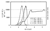
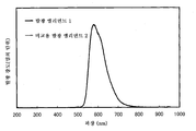
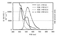
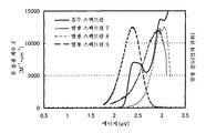
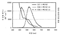
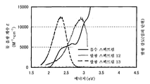
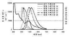
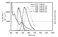
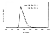
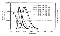
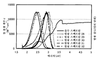
도 1a 및 도 1b는 각각 실시예 1에 의한 흡수 스펙트럼 및 발광 스펙트럼을 도시한다.
도 2a 및 2b는 각각 실시예 2에 의한 흡수 스펙트럼 및 발광 스펙트럼을 도시한다.
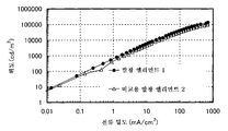
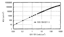
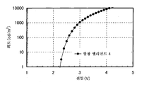
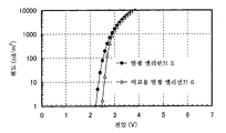
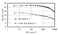
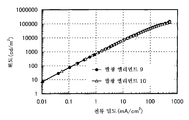
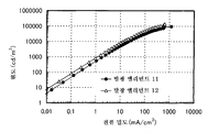
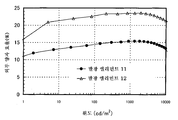
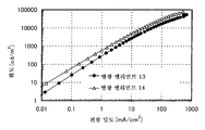
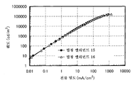
도 3은 실시예 3의 발광 엘리먼트의 전류 밀도-휘도 특징을 도시한다.
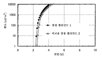
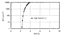
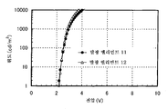
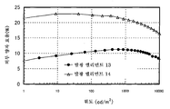
도 4는 실시예 3의 발광 엘리먼트의 전압-휘도 특징을 도시한다.
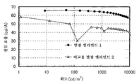
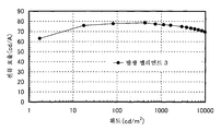
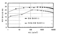
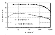
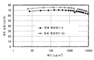
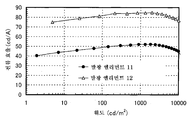
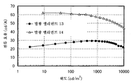
도 5는 실시예 3의 발광 엘리먼트의 휘도-전류 효율 특징을 도시한다.
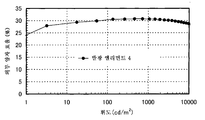
도 6은 실시예 3의 발광 엘리먼트의 휘도-외부 양자 효율 특징을 도시한다.
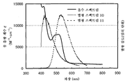
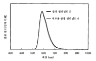
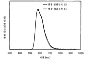
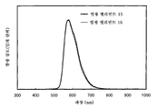
도 7은 실시예 3의 발광 엘리먼트의 발광 스펙트럼을 도시한다.
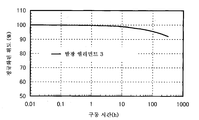
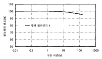
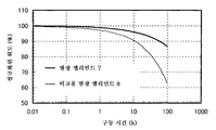
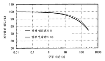
도 8은 실시예 3의 발광 엘리먼트의 신뢰성 테스트를 도시한다.
도 9는 실시예 4의 발광 엘리먼트의 전류 밀도-휘도 특징을 도시한다.
도 10은 실시예 4의 발광 엘리먼트의 전압-휘도 특징을 도시한다.
도 11은 실시예 4의 발광 엘리먼트의 휘도-전류 효율 특징을 도시한다.
도 12는 실시예 4의 발광 엘리먼트의 휘도-외부 양자 효율 특징을 도시한다.
도 13은 실시예 4의 발광 엘리먼트의 발광 스펙트럼을 도시한다.
도 14는 실시예 4의 발광 엘리먼트의 신뢰성 테스트를 도시한다.
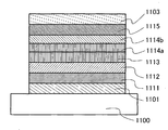
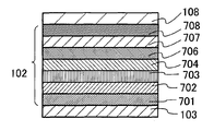
도 15는 실시예의 발광 엘리먼트의 구조를 도시한다.
도 16a 내지 도 16c는 각각 본 발명의 하나의 실시양태의 발광 엘리먼트를 도시한다.
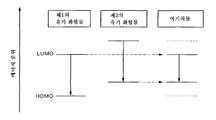
도 17은 본 발명의 하나의 실시양태에 적용된 여기착물의 에너지 준위를 도시한다.
도 18a 및 18b는 각각 실시예 5에 의한 흡수 스펙트럼 및 발광 스펙트럼을 도시한다.
도 19는 실시예 6의 발광 엘리먼트의 전류 밀도-휘도 특징을 도시한다.
도 20은 실시예 6의 발광 엘리먼트의 전압-휘도 특징을 도시한다.
도 21은 실시예 6의 발광 엘리먼트의 휘도-전류 효율 특징을 도시한다.
도 22는 실시예 6의 발광 엘리먼트의 휘도-외부 양자 효율 특징을 도시한다.
도 23은 실시예 6의 발광 엘리먼트의 발광 스펙트럼을 도시한다.
도 24는 실시예 6의 발광 엘리먼트의 신뢰성 테스트를 도시한다.
도 25는 본 발명의 하나의 실시형태의 개념을 도시한다.
도 26a 및 도 26b는 각각 실시예 7에 의한 흡수 스펙트럼 및 발광 스펙트럼을 도시한다.
도 27은 실시예 8의 발광 엘리먼트의 전류 밀도-휘도 특징을 도시한다.
도 28은 실시예 8의 발광 엘리먼트의 전압-휘도 특징을 도시한다.
도 29는 실시예 8의 발광 엘리먼트의 휘도-전류 효율 특징을 도시한다.
도 30은 실시예 8의 발광 엘리먼트의 휘도-외부 양자 효율 특징을 도시한다.
도 31은 실시예 8의 발광 엘리먼트의 발광 스펙트럼을 도시한다.
도 32a 및 도 32b는 각각 실시예 9에 의한 흡수 스펙트럼 및 발광 스펙트럼을 도시한다.
도 33은 실시예 10의 발광 엘리먼트의 전류 밀도-휘도 특징을 도시한다.
도 34는 실시예 10의 발광 엘리먼트의 전압-휘도 특징을 도시한다.
도 35는 실시예 10의 발광 엘리먼트의 휘도-전류 효율 특징을 도시한다.
도 36은 실시예 10의 발광 엘리먼트의 휘도-외부 양자 효율 특징을 도시한다.
도 37은 실시예 10의 발광 엘리먼트의 발광 스펙트럼을 도시한다.
도 38은 실시예 10의 발광 엘리먼트의 신뢰성 테스트를 도시한다.
도 39a 및 도 39b는 각각 실시예 11에 의한 흡수 및 발광 스펙트럼을 도시한다.
도 40은 실시예 12의 발광 엘리먼트의 전류 밀도-휘도 특징을 도시한다.
도 41은 실시예 12의 발광 엘리먼트의 전압-휘도 특징을 도시한다.
도 42는 실시예 12의 발광 엘리먼트의 휘도-전류 효율 특징을 도시한다.
도 43은 실시예 12의 발광 엘리먼트의 휘도-외부 양자 효율 특징을 도시한다.
도 44는 실시예 12의 발광 엘리먼트의 발광 스펙트럼을 도시한다.
도 45는 실시예 12의 발광 엘리먼트의 신뢰성 테스트를 도시한다.
도 46a 및 도 46b는 각각 실시예 13에 의한 흡수 스펙트럼 및 발광 스펙트럼을 도시한다.
도 47은 실시예 14의 발광 엘리먼트의 전류 밀도-휘도 특징을 도시한다.
도 48은 실시예 14의 발광 엘리먼트의 전압-휘도 특징을 도시한다.
도 49는 실시예 14의 발광 엘리먼트의 휘도-전류 효율 특징을 도시한다.
도 50은 실시예 14의 발광 엘리먼트의 휘도-외부 양자 효율 특징을 도시한다.
도 51은 실시예 14의 발광 엘리먼트의 발광 스펙트럼을 도시한다.
도 52a 및 도 52b는 각각 실시예 15에 의한 흡수 스펙트럼 및 발광 스펙트럼을 도시한다.
도 53은 실시예 16의 발광 엘리먼트의 전류 밀도-휘도 특징을 도시한다.
도 54는 실시예 16의 발광 엘리먼트의 전압-휘도 특징을 도시한다.
도 55는 실시예 16의 발광 엘리먼트의 휘도-전류 효율 특징을 도시한다.
도 56은 실시예 16의 발광 엘리먼트의 휘도-외부 양자 효율 특징을 도시한다.
도 57은 실시예 16의 발광 엘리먼트의 발광 스펙트럼을 도시한다.
도 58a 및 도 58b는 각각 실시예 17에 의한 흡수 스펙트럼 및 발광 스펙트럼을 도시한다.
도 59는 실시예 18의 발광 엘리먼트의 전류 밀도-휘도 특징을 도시한다.
도 60은 실시예 18의 발광 엘리먼트의 전압-휘도 특징을 도시한다.
도 61은 실시예 18의 발광 엘리먼트의 휘도-전류 효율 특징을 도시한다.
도 62는 실시예 18의 발광 엘리먼트의 휘도-외부 양자 효율 특징을 도시한다.
도 63은 실시예 18의 발광 엘리먼트의 발광 스펙트럼을 도시한다.
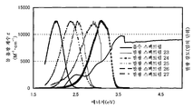
도 64는 본 발명의 하나의 실시형태에 의한 계산 결과를 도시한다.
도 65aa, 도 65ab, 도 65ba, 도 65bb, 도 65ca 및 도 65cb는 본 발명의 하나의 실시형태에 의한 계산 결과를 도시한다.1A and 1B show an absorption spectrum and an emission spectrum according to Example 1, respectively.
2A and 2B show absorption spectra and emission spectra according to Example 2, respectively.
FIG. 3 shows the current density-luminance characteristics of the light emitting element of Example 3.
4 shows the voltage-luminance characteristics of the light emitting element of Example 3.
5 shows the luminance-current efficiency characteristics of the light emitting element of Example 3.
FIG. 6 shows the luminance-external quantum efficiency characteristics of the light emitting element of Example 3.
7 shows the emission spectrum of the light emitting element of Example 3.
8 shows a reliability test of the light emitting element of Example 3.
9 shows the current density-luminance characteristics of the light emitting element of Example 4. FIG.
10 shows the voltage-luminance characteristics of the light emitting element of Example 4. FIG.
11 shows the luminance-current efficiency characteristics of the light emitting element of Example 4.
12 shows luminance-external quantum efficiency characteristics of the light emitting element of Example 4. FIG.
13 shows the emission spectrum of the light emitting element of Example 4. FIG.
14 shows a reliability test of the light emitting element of Example 4.
15 shows the structure of the light emitting element of the embodiment.
16A to 16C each show a light emitting element of one embodiment of the present invention.
17 shows the energy level of an excitation complex applied to one embodiment of the present invention.
18A and 18B show absorption spectra and emission spectra according to Example 5, respectively.
19 shows the current density-luminance characteristics of the light emitting element of Example 6.
20 shows the voltage-luminance characteristics of the light emitting element of Example 6.
21 shows the luminance-current efficiency characteristics of the light emitting element of Example 6.
22 shows the luminance-external quantum efficiency characteristics of the light emitting element of Example 6.
Fig. 23 shows the emission spectrum of the light emitting element of Example 6.
24 shows the reliability test of the light emitting element of Example 6.
25 shows the concept of one embodiment of the present invention.
26A and 26B show an absorption spectrum and an emission spectrum according to Example 7, respectively.
27 shows the current density-luminance characteristics of the light emitting element of Example 8.
28 shows voltage-luminance characteristics of the light emitting element of Example 8. FIG.
29 shows the luminance-current efficiency characteristics of the light emitting element of Example 8.
30 shows the luminance-external quantum efficiency characteristics of the light emitting element of Example 8.
31 shows the emission spectrum of the light emitting element of Example 8. FIG.
32A and 32B show the absorption spectrum and the emission spectrum according to Example 9, respectively.
33 shows the current density-luminance characteristics of the light emitting element of Example 10.
34 shows the voltage-luminance characteristics of the light emitting element of Example 10.
35 shows the luminance-current efficiency characteristics of the light emitting element of Example 10.
36 shows the luminance-external quantum efficiency characteristics of the light emitting element of Example 10.
37 shows the emission spectrum of the light emitting element of Example 10.
38 shows a reliability test of the light emitting element of Example 10.
39A and 39B show absorption and emission spectra according to Example 11, respectively.
40 shows the current density-luminance characteristics of the light emitting element of Example 12.
41 shows the voltage-luminance characteristics of the light emitting element of Example 12.
42 shows the luminance-current efficiency characteristics of the light emitting element of Example 12.
43 shows the luminance-external quantum efficiency characteristics of the light emitting element of Example 12.
44 shows the emission spectrum of the light emitting element of Example 12.
45 shows the reliability test of the light emitting element of Example 12.
46A and 46B show the absorption spectrum and emission spectrum according to Example 13, respectively.
47 shows the current density-luminance characteristics of the light emitting element of Example 14.
48 shows voltage-luminance characteristics of the light emitting element of Example 14.
49 shows the luminance-current efficiency characteristics of the light emitting element of Example 14.
50 shows luminance-external quantum efficiency characteristics of the light emitting element of Example 14.
51 shows the emission spectrum of the light emitting element of Example 14.
52A and 52B show the absorption spectrum and emission spectrum according to Example 15, respectively.
53 shows the current density-luminance characteristics of the light emitting element of Example 16.
54 shows the voltage-luminance characteristics of the light emitting element of Example 16.
55 shows the luminance-current efficiency characteristics of the light emitting element of Example 16.
56 shows the luminance-external quantum efficiency characteristics of the light emitting element of Example 16.
57 shows the emission spectrum of the light emitting element of Example 16.
58A and 58B show the absorption spectrum and emission spectrum according to Example 17, respectively.
59 shows the current density-luminance characteristics of the light emitting element of Example 18.
FIG. 60 shows the voltage-luminance characteristics of the light emitting element of Example 18.
61 shows the luminance-current efficiency characteristics of the light emitting element of Example 18.
FIG. 62 shows the luminance-external quantum efficiency characteristics of the light emitting element of Example 18.
Fig. 63 shows the emission spectrum of the light emitting element of Example 18.
64 shows calculation results according to one embodiment of the present invention.
65aa, 65ab, 65ba, 65bb, 65ca and 65cb show the calculation result according to one embodiment of the present invention.
실시형태는 도면을 참조하여 기재할 것이다. 본 발명은 하기의 상세한 설명에 한정되지 않는 점에 유의하며 그리고 본 발명의 정신 및 범주로부터 벗어남이 없이 다양한 변경예 및 수정예가 가능할 수 있는 것으로 당업자는 용이하게 이해할 것이다. 그러므로, 본 발명은 하기 실시형태에서의 기재내용으로 한정되는 것으로 해석되지 않아야 한다. 하기 기재된 본 발명의 구조에서, 동일한 부분 또는 유사한 기능을 갖는 부분은 동일한 부호를 상이한 도면에서 표기하며, 그러한 부분의 설명은 반복하지 않는다.Embodiments will be described with reference to the drawings. It should be noted that the present invention is not limited to the following detailed description, and those skilled in the art will readily understand that various modifications and modifications can be made without departing from the spirit and scope of the present invention. Therefore, the present invention should not be construed as being limited to the description in the following embodiments. In the structure of the present invention described below, parts having the same or similar functions are denoted by the same reference numerals in different drawings, and the description of such parts is not repeated.
실시형태 1
본 실시형태에서, 본 발명의 하나의 실시형태의 발광 엘리먼트를 기재할 것이다.In this embodiment, the light emitting element of one embodiment of the present invention will be described.
본 실시형태의 발광 엘리먼트는 발광 물질인 게스트 물질, 제1의 유기 화합물 및 제2의 유기 화합물을 함유하는 발광층을 포함한다. 구체적으로는, 인광 화합물은 게스트 물질로서 사용된다. 제1의 및 제2의 유기 화합물 중 하나에서 발광층에 포함된 비율이 다른 하나보다 더 큰 것을 호스트 물질로 지칭한다는 점에 유의한다.The light emitting element of this embodiment includes a light emitting layer containing a guest material that is a light emitting material, a first organic compound, and a second organic compound. Specifically, a phosphorescent compound is used as a guest material. Note that, in one of the first and second organic compounds, the ratio included in the light emitting layer is greater than the other, and is referred to as a host material.
게스트 물질이 호스트 물질 중에 분산된 구조는 발광층이 결정화되는 것을 방지할 수 있다. 추가로, 게스트 물질의 농도가 높음으로 인하여 농도 소광을 억제할 수 있으며, 그래서 발광 엘리먼트는 발광 효율이 더 높을 수 있다.The structure in which the guest material is dispersed in the host material can prevent the light emitting layer from crystallizing. In addition, due to the high concentration of the guest material, concentration quenching can be suppressed, so that the light emitting element can have higher light emission efficiency.
본 실시형태에서, 제1의 및 제2의 유기 화합물 각각의 삼중항 여기 에너지의 준위(T1 준위)는 게스트 물질보다 높은 것이 바람직하다는 점에 유의한다. 이는 제1의 유기 화합물(또는 제2의 유기 화합물)의 T1 준위가 게스트 물질보다 더 낮으며, 발광에 기여하는 게스트 물질의 삼중항 여기 에너지는 제1의 유기 화합물(또는 제2의 유기 화합물)에 의하여 소광되며, 그리하여 발광 효율이 감소되기 때문이다.Note that in this embodiment, the level of the triplet excitation energy (T 1 level) of each of the first and second organic compounds is preferably higher than the guest material. This means that the T 1 level of the first organic compound (or the second organic compound) is lower than that of the guest material, and the triplet excitation energy of the guest material that contributes to light emission is the first organic compound (or the second organic compound). This is because it is extinguished by), and thus the luminous efficiency is reduced.
<발광의 기본 과정><Basic process of luminescence>
우선, 인광 화합물을 게스트 물질로서 사용한 발광 엘리먼트에서의 발광의 일반적인 기본 과정을 설명한다.First, a general basic process of light emission in a light emitting element using a phosphorescent compound as a guest material will be described.
(1) 전자 및 정공이 게스트 분자내에서 재결합되고, 게스트 분자가 여기되는 경우(직접 재결합 과정).(1) When electrons and holes are recombined in the guest molecule, and the guest molecule is excited (direct recombination process).
(1-1) 게스트 분자의 여기 상태가 삼중항 여기 상태일 때, 게스트 분자가 인광을 발광한다.(1-1) When the excited state of the guest molecule is a triplet excited state, the guest molecule emits phosphorescence.
(1-2) 게스트 분자의 여기 상태가 일중항 여기 상태일 때, 일중항 여기 상태의 게스트 분자는 삼중항 여기 상태에 항간(intersystem) 교차되고, 인광을 발광한다.(1-2) When the excited state of the guest molecule is a singlet excited state, the guest molecule of the singlet excited state intersystem crosses the triplet excited state and emits phosphorescence.
환언하면, (1)에서의 직접 재결합 과정에서, 게스트 분자의 항간 교차 및 인광 양자 효율이 높은 한, 높은 발광 효율을 얻을 수 있다. 상기 기재한 바와 같이, 호스트 분자의 T1 준위는 게스트 분자의 T1 준위보다 높은 것이 바람직하다는 것에 유의한다.In other words, in the direct recombination process in (1), a high luminous efficiency can be obtained as long as the inter-crossing and phosphorescence quantum efficiency of the guest molecule is high. As described above, T 1 level of the host molecule is noted that preferably higher than the T 1 level of the guest molecule.
(2) 전자 및 정공이 호스트 분자에서 재결합되어 호스트 분자가 여기 상태가 되는 경우(에너지 이동 과정).(2) When electrons and holes recombine in the host molecule and the host molecule is excited (energy transfer process).
(2-1) 호스트 분자의 여기 상태가 삼중항 여기 상태이고 그리고 호스트 분자의 T1 준위가 게스트 분자보다 높을 때, 여기 에너지는 호스트 분자로부터 게스트 분자로 이동되며, 그리하여 게스트 분자는 삼중항 여기 상태가 된다. 삼중항 여기 상태인 게스트 분자는 인광을 발광한다. 게스트 분자의 일중항 여기 에너지 준위(S1 준위)로의 에너지 이동이 이론상 발생할 수 있으나, 다수의 경우에서 게스트 분자의 S1 준위가 호스트 분자의 T1 준위보다 에너지가 더 높기 때문에 주요 에너지 이동 과정이 발생할 것 같지 않다는 점에 유의하며, 그러므로, 그의 설명은 여기서 제시하지 않는다.(2-1) When the excitation state of the host molecule is a triplet excitation state and the T 1 level of the host molecule is higher than the guest molecule, excitation energy is transferred from the host molecule to the guest molecule, so that the guest molecule is a triplet excitation state Becomes The guest molecule in the triplet excited state emits phosphorescence. The transfer of energy from the guest molecule to the singlet excitation energy level (S 1 level) may theoretically occur, but in many cases the main energy transfer process is due to the fact that the S 1 level of the guest molecule is higher than the T 1 level of the host molecule. Note that it is unlikely to occur, and therefore, its explanation is not given here.
(2-2) 호스트 분자의 여기 상태가 일중항 여기 상태이고 그리고 호스트 분자의 S1 준위가 게스트 분자의 S1 준위 및 T1 준위보다 더 높을 때, 여기 에너지는 호스트 분자로부터 게스트 분자로 이동되며, 그리하여 게스트 분자는 일중항 여기 상태 또는 삼중항 여기 상태가 된다. 삼중항 여기 상태의 게스트 분자는 인광을 발광한다. 게다가, 일중항 여기 상태의 게스트 분자는 삼중항 여기 상태로 항간 교차되어 인광을 발광한다.(2-2) When the excited state of the host molecule is a singlet excited state and the S 1 level of the host molecule is higher than the S 1 level and the T 1 level of the guest molecule, the excitation energy is transferred from the host molecule to the guest molecule , Thus the guest molecule is either singlet excited or triplet excited. The guest molecule in the triplet excited state emits phosphorescence. In addition, the guest molecule in the singlet excited state intersects the triplet excited state to emit phosphorescence.
환언하면, (2)에서의 에너지 이동 과정에서, 호스트 분자의 삼중항 여기 에너지 및 일중항 여기 에너지 모두가 어떻게 게스트 분자로 효율적으로 이동될 수 있느냐가 중요하다.In other words, in the energy transfer process in (2), it is important how both the triplet excitation energy and singlet excitation energy of the host molecule can be efficiently transferred to the guest molecule.
상기 기재한 에너지 이동 과정을 감안하면, 호스트 분자의 여기 에너지가 게스트 분자로 이동되기 이전에, 호스트 분자 그 자체가 광 또는 열로서 여기 에너지를 발광하여 탈활성화될 때, 발광 효율이 감소된다. 본 발명자들은 호스트 분자가 일중항 여기 상태에 있을 때(상기 (2-2))는 호스트 분자가 삼중항 여기 상태에 있을 때(상기 (2-1))에 비하여 에너지는 인광 화합물인 게스트 분자로 이동되지 않을 것이며, 발광 효율이 감소되기 쉽다는 것을 알아냈다. 그래서, 본 발명자들은 과제로서 그러한 사실에 주목하였다. 그의 이유는 보다 상세한 에너지 이동 과정을 고려하여 하기와 같이 발견되었다.Given the energy transfer process described above, before the excitation energy of the host molecule is transferred to the guest molecule, the luminous efficiency is reduced when the host molecule itself is deactivated by emitting excitation energy as light or heat. The present inventors show that when the host molecule is in the singlet excited state (above (2-2)), the energy is a guest molecule that is a phosphorescent compound compared to when the host molecule is in the triplet excited state ((2-1) above). It has been found that it will not move and the luminous efficiency is likely to decrease. So, the present inventors paid attention to such a fact as a subject. His reason was found as follows in consideration of a more detailed energy transfer process.
<에너지 이동 과정><Energy Transfer Process>
하기는 분자간 에너지 이동 과정을 상세하게 설명한다.The following describes the intermolecular energy transfer process in detail.
우선, 분자간 에너지 이동의 메카니즘으로서, 하기 2가지 메카니즘을 제안한다. 여기 에너지를 제공하는 분자를 호스트 분자로서 지칭하며, 여기 에너지를 받는 분자는 게스트 분자로서 지칭한다.First, as a mechanism of intermolecular energy transfer, the following two mechanisms are proposed. A molecule that provides excitation energy is referred to as a host molecule, and a molecule that receives excitation energy is referred to as a guest molecule.
≪포스터(Foerster) 메카니즘(쌍극자-쌍극자 상호작용)≫≪Foerster mechanism (dipole-dipole interaction) ≫
포스터 메카니즘(또한 포스터 공명 에너지 이동으로도 지칭됨)에서, 분자간 직접 접촉은 에너지 이동에 필요하지 않다. 호스트 분자 및 게스트 분자 사이의 쌍극자 진동의 공명 현상을 통하여 에너지 이동이 발생한다. 쌍극자 진동의 공명 현상에 의하여, 호스트 분자는 게스트 분자에 에너지를 제공하여 호스트 분자가 기저 상태가 되며, 게스트 분자는 여기 상태가 된다. 포스터 메카니즘의 속도 상수 kh*→g는 하기 수학식 1로 나타낸다:In the poster mechanism (also referred to as poster resonance energy transfer), intermolecular direct contact is not required for energy transfer. Energy transfer occurs through the resonance phenomenon of dipole vibration between the host molecule and the guest molecule. Due to the resonance phenomenon of dipole vibration, the host molecule provides energy to the guest molecule, so that the host molecule is in a ground state, and the guest molecule is in an excited state. The rate constant k h * → g of the poster mechanism is represented by
<수학식 1><

수학식 1에서, ν는 진동수를 나타내며, f'h(ν)는 호스트 분자의 정규화된 발광 스펙트럼(일중항 여기 상태로부터의 에너지 이동에서의 형광 스펙트럼 및 삼중항 여기 상태로부터의 에너지 이동에서의 인광 스펙트럼)을 나타내며, εg(ν)는 게스트 분자의 몰 흡광 계수를 나타내며, N은 아보가드로의 수를 나타내며, n은 매체의 굴절율을 나타내며, R은 호스트 분자 및 게스트 분자 사이의 분자간 거리를 나타내며, τ는 여기 상태의 측정된 수명(형광 수명 또는 인광 수명)을 나타내며, c는 광속을 나타내며, φ는 발광 양자 효율(일중항 여기 상태로부터 에너지 이동에서의 형광 양자 효율 및 삼중항 여기 상태로부터 에너지 이동에서의 인광 양자 효율)을 나타내며, K2는 호스트 분자 및 게스트 분자 사이의 전이 쌍극자 모멘트의 배향의 계수(0 내지 4)를 나타낸다. 랜덤 배향의 경우 K2=2/3인 것에 유의한다.In
≪덱스터(Dexter) 메카니즘(전자 교환 상호작용)≫≪Dexter mechanism (electronic exchange interaction) ≫
덱스터 메카니즘(또한 덱스터 전자 이동으로 지칭함)에서, 호스트 분자 및 게스트 분자는 그의 궤도의 중첩이 발생하는 접촉 유효 범위에 근접하며, 여기 상태에서의 호스트 분자 및 기저 상태에서의 게스트 분자의 전자 교환을 통하여 에너지 이동이 발생한다. 덱스터 메카니즘의 속도 상수 kh*→g는 하기 수학식 2로 나타낸다:In the Dexter mechanism (also referred to as Dexter electron transfer), the host molecule and the guest molecule are close to the contact effective range where their orbital overlap occurs, through the electron exchange of the host molecule in the excited state and the guest molecule in the ground state. Energy transfer occurs. The rate constant k h * → g of the Dexter mechanism is represented by
<수학식 2><

수학식 2에서, h는 플랑크(Planck) 상수를 나타내며, K는 에너지의 차원을 갖는 상수를 나타내며, ν는 진동수를 나타내며, f'h(ν)는 호스트 분자의 정규화된 발광 스펙트럼(일중항 여기 상태로부터의 에너지 이동에서의 형광 스펙트럼 및 삼중항 여기 상태로부터의 에너지 이동에서의 인광 스펙트럼)을 나타내며, ε'g(ν)는 게스트 분자의 정규화된 흡수 스펙트럼을 나타내며, L은 유효 분자 반경을 나타내며, R은 호스트 분자 및 게스트 분자 사이의 분자간 거리를 나타낸다.In
여기서, 호스트 분자로부터 게스트 분자로의 에너지 이동의 효율 ΦET(에너지 이동 효율 ΦET)은 하기 화학식 3으로 나타내는 것으로 생각된다. 화학식 3에서, kr은 호스트 분자의 발광 과정(일중항 여기 상태로부터의 에너지 이동에서의 형광 및 삼중항 여기 상태로부터의 에너지 이동에서의 인광)의 속도 상수를 나타내며, kn은 호스트 분자의 비발광 과정(열 불활성화 또는 항간 교차)의 속도 상수를 나타내며, τ는 호스트 분자의 여기 상태의 측정된 수명을 나타낸다:Here, the efficiency of energy transfer from the host molecule to the guest molecule Φ ET (energy transfer efficiency Φ ET ) is considered to be represented by the following formula (3). In
<수학식 3><

우선, 수학식 3에 의하면, 또다른 경합하는 속도 상수 kr + kn (= 1/τ)에 비하여 에너지 이동의 속도 상수 kh*→g를 추가로 증가시킴으로써 에너지 이동 효율 ΦET는 증가될 수 있는 것으로 밝혀졌다. 그후, 에너지 이동의 속도 상수 kh*→g를 증가시키기 위하여, 수학식 1 및 수학식 2에 기초하여 포스터 메카니즘 및 덱스터 메카니즘에서 호스트 분자의 발광 스펙트럼(일중항 여기 상태로부터 에너지 이동에서의 형광 스펙트럼 및 삼중항 여기 상태로부터 에너지 이동에서의 인광 스펙트럼)은 게스트 분자의 흡수 스펙트럼과 크게 중첩되는 것이 바람직하다.First, according to
여기서, 본 발명자들은 호스트 분자의 발광 스펙트럼 및 게스트 분자의 흡수 스펙트럼 사이의 중첩을 고려하여 게스트 분자의 흡수 스펙트럼에서의 최장 파장측(최저 에너지측)에서의 흡수 밴드가 중요하다고 생각하였다.Here, the inventors considered that the absorption band at the longest wavelength side (lowest energy side) in the absorption spectrum of the guest molecule is important in consideration of the overlap between the emission spectrum of the host molecule and the absorption spectrum of the guest molecule.
본 실시형태에서, 인광 화합물은 게스트 물질로서 사용된다. 인광 화합물의 흡수 스펙트럼에서, 발광에 가장 크게 기여하는 것으로 고려되는 흡수 밴드는 일중항 기저 상태로부터 삼중항 여기 상태로의 직접 전이에 해당하는 흡수 파장과 그의 부근에 있으며, 이는 최장 파장측에 있는 흡수 밴드에 있다. 그러므로, 호스트 물질의 발광 스펙트럼(형광 스펙트럼 및 인광 스펙트럼)은 인광 화합물의 흡수 스펙트럼에서 최장 파장측의 흡수 밴드와 중첩되는 것이 바람직한 것으로 고려된다.In this embodiment, a phosphorescent compound is used as the guest material. In the absorption spectrum of the phosphorescent compound, the absorption band considered to be the largest contributor to luminescence is at and near the absorption wavelength corresponding to the direct transition from the singlet ground state to the triplet excited state, which is the absorption at the longest wavelength side. In the band. Therefore, it is considered preferable that the emission spectrum (fluorescence spectrum and phosphorescence spectrum) of the host material overlaps with the absorption band on the longest wavelength side in the absorption spectrum of the phosphorescent compound.
예를 들면, 대부분의 유기금속 착물, 특히 발광 이리듐 착물은 최장 파장측의 흡수 밴드로서 약 500 ㎚ 내지 600 ㎚에서 넓은 흡수 밴드를 갖는다(사실상, 넓은 흡수 밴드는 발광 파장에 의존하여 더 짧거나 또는 더 긴 파장측에 존재할 수 있다). 이러한 흡수 밴드는 주로 삼중항 MLCT(금속 대 리간드 전하 이동) 전이에 기초한다. 흡수 밴드는 또한 삼중항 π-π* 전이 및 일중항 MLCT 전이에 기초한 흡수를 포함하며, 이러한 흡수가 서로에 대하여 중첩되어 흡수 스펙트럼에서 최장 파장측에 넓은 흡수 밴드를 형성하는 것으로 고려된다는 점에 유의한다. 환언하면, 최저 일중항 여기 상태 및 최저 삼중항 여기 상태 사이의 차이는 작으며, 이들 상태에 기초한 흡수는 서로 중첩되어 흡수 스펙트럼에서 최장 파장측에 넓은 흡수 밴드를 형성한다. 그러므로, 상기 기재한 바와 같이, 유기금속 착물(특히 이리듐 착물)이 게스트 물질로서 사용되는 경우 최장 파장측에서의 넓은 흡수 밴드는 호스트 물질의 발광 스펙트럼과 크게 중첩되는 것이 바람직하다.For example, most organometallic complexes, especially luminescent iridium complexes, have broad absorption bands from about 500 nm to 600 nm as absorption bands on the longest wavelength side (in fact, the broad absorption bands are shorter or depend on the emission wavelength) May be on the longer wavelength side). This absorption band is mainly based on triplet MLCT (metal to ligand charge transfer) transitions. Note that the absorption band also includes absorption based on triplet π-π * transitions and singlet MLCT transitions, and these absorptions are considered to overlap with each other to form a wide absorption band on the longest wavelength side in the absorption spectrum. do. In other words, the difference between the lowest singlet excited state and the lowest triplet excited state is small, and the absorptions based on these states overlap each other to form a wide absorption band on the longest wavelength side in the absorption spectrum. Therefore, as described above, when an organometallic complex (especially an iridium complex) is used as a guest material, it is preferable that the wide absorption band at the longest wavelength side largely overlaps with the emission spectrum of the host material.
여기서, 우선, 호스트 물질의 삼중항 여기 상태로부터의 에너지 이동을 고려할 것이다. 상기 기재한 논의로부터, 삼중항 여기 상태로부터의 에너지 이동에서 호스트 물질의 인광 스펙트럼 및 게스트 물질의 최장 파장측에서의 흡수 밴드는 서로 크게 중첩되는 것이 바람직하다.Here, first, the energy transfer from the triplet excited state of the host material will be considered. From the discussion described above, it is preferable that the phosphorescence spectrum of the host material in the energy transfer from the triplet excited state and the absorption bands at the longest wavelength side of the guest material overlap greatly with each other.
형광 화합물은 일반적으로 호스트 물질로서 사용되며; 그리하여 인광 수명(τ)은 밀리초 또는 매우 크게 길다(즉, kr + kn이 낮다)는 점에 유의한다. 이는 삼중항 여기 상태로부터 기저 상태(일중항)로의 전이가 금지된 전이이기 때문이다. 상기 수학식 3은 에너지 이동 효율 ΦET에 대하여 유리하다는 것을 나타낸다. 이는 또한 일반적으로 삼중항 여기 상태의 호스트 물질로부터 삼중항 여기 상태의 게스트 물질로 에너지가 이동된다는 것을 시사한다.Fluorescent compounds are generally used as host materials; It is thus noted that the phosphorescence lifetime τ is milliseconds or very large (i.e., k r + k n is low). This is because the transition from the triplet excited state to the ground state (single term) is forbidden.
그러나, 여기서 문제가 되는 것은 일중항 여기 상태의 호스트 물질로부터의 에너지 이동이다. 삼중항 여기 상태로부터의 에너지 이동뿐 아니라, 일중항 여기 상태로부터의 에너지 이동을 효율적으로 수행하기 위하여, 호스트 물질은 그의 인광 스펙트럼뿐 아니라, 형광 스펙트럼을 게스트 물질의 최장 파장측에서 흡수 밴드와 중첩되도록 설계되어야만 한다는 것은 상기 기재된 논의로부터 명백하다. 환언하면, 호스트 물질의 형광 스펙트럼이 그의 인광 스펙트럼과 유사한 위치를 갖도록 호스트 물질을 설계하지 않을 경우, 일중항 여기 상태 및 삼중항 여기 상태 모두에서 호스트 물질로부터 효과적인 에너지 이동을 달성할 수 없다.However, the problem here is the energy transfer from the host material in the singlet excited state. In order to efficiently perform energy transfer from the triplet excited state, as well as energy transfer from the singlet excited state, the host material is such that its phosphorescence spectrum, as well as its fluorescence spectrum, overlap the absorption band at the longest wavelength side of the guest material. It should be apparent from the discussion described above that it should be designed. In other words, if the host material is not designed such that the fluorescence spectrum of the host material has a position similar to its phosphorescence spectrum, effective energy transfer from the host material cannot be achieved in both singlet and triplet excited states.
그러나, S1 준위는 일반적으로 T1 준위와는 크게 상이하며(S1 준위 > T1 준위); 그래서, 형광 발광 파장은 또한 인광 발광 파장과는 크게 상이하다(형광 발광 파장<인광 발광 파장). 예를 들면, 인광 화합물을 포함하는 발광 엘리먼트에서 호스트 물질로서 통상적으로 사용되는 4,4'-디(N-카르바졸릴)비페닐(약어: CBP)은 약 500 ㎚에서 인광 스펙트럼을 가지며, 약 400 ㎚에서 형광 스펙트럼을 갖는데, 이들은 약 100 ㎚ 정도 차이가 있다. 이러한 예는 또한 호스트 물질의 형광 스펙트럼이 인광 스펙트럼과 유사한 위치에 있도록 호스트 물질을 설계하는 것이 매우 곤란하다는 것을 나타낸다. 그러므로, 본 발명자들은 일중항 여기 상태에서의 호스트 물질로부터 게스트 물질로의 에너지 이동에서의 효율을 개선시키는 것은 주요한 과제가 되는 것으로 고려된다.However, the S 1 level is generally significantly different from the T 1 level (S 1 level> T 1 level); Thus, the fluorescence emission wavelength is also significantly different from the phosphorescence emission wavelength (fluorescence emission wavelength <phosphorescence emission wavelength). For example, 4,4'-di (N-carbazolyl) biphenyl (abbreviation: CBP), which is commonly used as a host material in a light emitting element comprising a phosphorescent compound, has a phosphorescence spectrum at about 500 nm, about It has a fluorescence spectrum at 400 nm, which differs by about 100 nm. This example also indicates that it is very difficult to design the host material so that the fluorescence spectrum of the host material is in a position similar to the phosphorescence spectrum. Therefore, it is considered by the inventors that improving efficiency in energy transfer from the host material to the guest material in the singlet excited state is a major challenge.
호스트 물질로서 사용되는 형광 화합물의 형광 수명(τ)이 나노초 정도로 매우 짧다(즉, kr + kn이 높다)는 점에 유의한다. 이는 일중항 여기 상태로부터 기저 상태(일중항)로의 전이가 허용된 전이이기 때문이다. 상기 화학식 3은 에너지 이동 효율 ΦET에 대하여 불리하다는 것을 나타낸다. 이는 또한 에너지가 일중항 여기 상태의 호스트 물질로부터 게스트 물질로 에너지가 이동되는 것이 일반적으로 발생되지 않다는 것을 시사한다.Note that the fluorescence lifetime (τ) of the fluorescent compound used as the host material is very short (i.e., k r + k n is high) in nanoseconds. This is because the transition from the singlet excited state to the ground state (single term) is an allowed transition.
본 발명의 하나의 실시형태는 일중항 여기 상태의 호스트 물질로부터 게스트 물질로의 에너지 이동 효율의 문제점을 극복할 수 있는 유용한 기술이 된다.One embodiment of the present invention is a useful technique that can overcome the problem of energy transfer efficiency from host material in singlet excited state to guest material.
지금까지는 인광 화합물은 항간 교차가 단일 여기 상태 및 삼중항 여기 상태 모두를 발광으로 변환시킬 수 있으므로(상기 기재된 "(1) 직접 재결합 과정"으로 지칭함), 인광 화합물을 포함하는 발광 엘리먼트는 내부 양자 효율이 이론적으로 100%를 달성할 수 있는 것으로 고려되는 것에 유의한다. 게다가, 광 추출 효율이 20%이라는 가정하에서 외부 양자 효율이 20%인 발광 엘리먼트는 실질적으로 100%의 내부 양자 효율을 달성한 것으로 논의되었다. 그러나, 사실상 호스트 물질의 일중항 여기 상태로부터의 상기 기재된 에너지 이동이 간과되었으므로, 이러한 통상의 발광 엘리먼트는 100%의 내부 양자 효율을 달성하지 않은 것으로 고려된다. 이는 본 발명자가 하기 기재한 본 발명의 실시형태를 수행함으로써 30%의 외부 양자 효율을 달성하였다는 사실에 기초한다. 환언하면, 30% 이상의 외부 양자 효율은 100%의 내부 양자 효율에 해당하며, 본 발명의 하나의 실시형태는 이를 달성하기 위한 유용한 기술이 된다. 이는 20%의 통상의 외부 양자 효율이 70% 이하의 내부 양자 효율에 해당하는 것으로 추정할 수 있다는 것을 나타낸다는 점에 유의한다.So far, the phosphorescent compound can convert both the single-excitation state and the triplet-excitation state of the inter-crossing into light emission (referred to as "(1) direct recombination process" described above), so that the light-emitting element comprising the phosphorescent compound has internal quantum efficiency. Note that it is considered that this theoretically can achieve 100%. Moreover, under the assumption that the light extraction efficiency is 20%, a light emitting element having an external quantum efficiency of 20% was discussed as having achieved an internal quantum efficiency of substantially 100%. However, since the energy transfer described above from the singlet excited state of the host material is in fact overlooked, it is considered that this conventional light emitting element does not achieve an internal quantum efficiency of 100%. This is based on the fact that the inventor achieved an external quantum efficiency of 30% by carrying out the embodiments of the invention described below. In other words, an external quantum efficiency of 30% or more corresponds to an internal quantum efficiency of 100%, and one embodiment of the present invention is a useful technique for achieving this. Note that this indicates that a typical external quantum efficiency of 20% can be estimated to correspond to an internal quantum efficiency of 70% or less.
<본 발명의 하나의 실시형태><One embodiment of the present invention>
본 발명의 하나의 실시형태는 인광 화합물, 제1의 유기 화합물 및 제2의 유기 화합물을 포함하는 발광층을 한쌍의 전극 사이에 포함하며, 제1의 유기 화합물 및 제2의 유기 화합물의 조합이 여기착물을 형성하는 발광 엘리먼트이다.One embodiment of the present invention comprises a light emitting layer comprising a phosphorescent compound, a first organic compound and a second organic compound between a pair of electrodes, wherein the combination of the first organic compound and the second organic compound is excited. It is a light-emitting element forming a complex.
제1의 유기 화합물 및 제2의 유기 화합물은 캐리어 재결합을 통하여 (또는 일중항 여기자로부터) 여기착물(또한 여기된 착물로 지칭됨)을 형성한다. 형성된 여기착물이 발광되는 경우, 그의 발광 파장은 각각의 제1의 및 제2의 유기 화합물의 발광 파장(형광 파장)에 대하여 더 긴 파장측에 위치한다. 환언하면, 여기착물의 형성에 의하여, 제1의 유기 화합물의 형광 스펙트럼 및 제2의 유기 화합물의 형광 스펙트럼은 더 긴 파장측에 위치하는 발광 스펙트럼으로 변환될 수 있다.The first organic compound and the second organic compound form an excitation complex (also referred to as an excited complex) through carrier recombination (or from singlet excitons). When the formed excitation complex emits light, its emission wavelength is located on the longer wavelength side with respect to the emission wavelength (fluorescence wavelength) of each of the first and second organic compounds. In other words, by formation of the excitation complex, the fluorescence spectrum of the first organic compound and the fluorescence spectrum of the second organic compound can be converted into an emission spectrum located on the longer wavelength side.
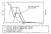
그러므로, 도 25에 예시한 바와 같이, 제1의 유기 화합물(또는 제2의 유기 화합물)의 형광 스펙트럼이 최장 파장측에 위치하는 인광 화합물의 흡수 밴드에 대하여 더 짧은 파장측에 위치하며 그리고 흡수 밴드와 중첩되지 않는 경우조차, 흡수 밴드와의 중첩이 크도록 여기착물을 형성하여 긴 파장을 갖는 발광 스펙트럼을 얻을 수 있다. 본 발명의 하나의 실시형태의 발광 엘리먼트는 여기착물의 발광 스펙트럼 및 인광 화합물의 흡수 스펙트럼 사이의 중첩을 사용하여 에너지를 이동시키므로 에너지 이동 효율이 높다. 그러므로, 본 발명의 하나의 실시형태에서, 외부 양자 효율이 높은 발광 엘리먼트를 얻을 수 있다.Therefore, as illustrated in FIG. 25, the fluorescence spectrum of the first organic compound (or the second organic compound) is located on the shorter wavelength side with respect to the absorption band of the phosphorescent compound located on the longest wavelength side, and the absorption band Even when not overlapping with, the excitation complex is formed so that the overlap with the absorption band is large, so that an emission spectrum having a long wavelength can be obtained. The light emitting element of one embodiment of the present invention transfers energy by using an overlap between the emission spectrum of the excitation complex and the absorption spectrum of the phosphorescent compound, and thus has high energy transfer efficiency. Therefore, in one embodiment of the present invention, a light emitting element with high external quantum efficiency can be obtained.
게다가, 여기착물은 여기 상태에서만 존재하므로 에너지를 흡수할 수 있는 기저 상태를 갖지 않는다. 그러므로, 인광 화합물의 일중항 여기 상태 및 삼중항 여기 상태이 여기착물로 역에너지 이동에 의하여 인광 화합물이 발광전 불활성화되는(즉 발광 효율이 저하됨) 현상은 원칙적으로 발생하지 않는 것으로 고려된다. 이는 또한 외부 양자 효율의 개선에 기여한다.Moreover, since the excitation complex exists only in the excited state, it does not have a ground state capable of absorbing energy. Therefore, it is considered that, in principle, the phenomenon that the singlet excited state and the triplet excited state of the phosphorescent compound is deactivated (ie, the luminous efficiency is lowered) before the light emission by reverse energy transfer to the excitation complex does not occur. This also contributes to the improvement of external quantum efficiency.
게다가, 여기착물은 일중항 여기된 에너지 및 삼중항 여기된 에너지 사이의 차이가 매우 작은 것으로 고려된다. 환언하면, 단일 상태로부터의 여기착물의 발광 스펙트럼 및 삼중항 상태로부터의 발광 스펙트럼은 서로 매우 근접하다. 따라서, 여기착물의 발광 스펙트럼(일반적으로 일중항 상태로부터의 여기착물의 발광 스펙트럼)이 상기 기재한 바와 같이 최장 파장측에서 인광 화합물의 흡수 밴드와 중첩되도록 설계를 수행하는 경우, 여기착물의 삼중항 상태로부터의 발광 스펙트럼(실온에서 관찰되지 않으며 그리고 다수의 경우에서 저온에서조차 관찰되지 않음)은 또한 최장 파장측에 위치하는 인광 화합물의 흡수 밴드와 중첩된다. 보다 구체적으로는, 이는 여기착물로부터 일중항 상태 및 삼중항 상태 모두에서 인광 화합물에 대하여 효율적으로 에너지를 이동시킬 수 있다는 것을 의미한다.Moreover, the excitation complex is considered to have a very small difference between singlet excited energy and triplet excited energy. In other words, the emission spectrum from the singlet state and the emission spectrum from the triplet state are very close to each other. Therefore, when the design is performed such that the emission spectrum of the excitation complex (generally, the emission spectrum of the excitation complex from the singlet state) overlaps the absorption band of the phosphorescent compound at the longest wavelength side as described above, the triplet of the excitation complex The emission spectrum from the state (not observed at room temperature and not even at low temperature in many cases) also overlaps the absorption band of the phosphorescent compound located on the longest wavelength side. More specifically, this means that the energy can be efficiently transferred to the phosphorescent compound in both singlet and triplet states from the excitation complex.
실제로 여기착물이 상기 특징을 갖는지에 대하여 하기 기재된 바와 같이 분자 궤도 계산을 수행하였다. 일반적으로, 헤테로방향족 화합물 및 방향족 아민의 조합은 종종 방향족 아민의 최저 비점유 분자 궤도(LUMO) 준위보다 더 깊은 헤테로방향족 화합물의 LUMO 준위(전자를 쉽게 수용하는 성질) 및 헤테로방향족 화합물의 최고 점유 분자 궤도(HOMO) 준위보다 더 얕은 방향족 아민의 HOMO 준위(정공을 쉽게 수용하는 성질)의 영향하에서 여기착물을 형성한다. 그래서, 헤테로방향족 화합물의 LUMO를 형성하는 대표적인 골격인 디벤조[f,h]퀴녹살린(약어: DBq) 및 방향족 아민의 HOMO를 형성하는 대표적인 골격인 트리페닐아민(약어: TPA)의 조합을 사용하여 계산하였다.Molecular orbital calculations were performed as described below with regard to whether the excitation complex actually had the above characteristics. In general, a combination of a heteroaromatic compound and an aromatic amine is often the LUMO level of a heteroaromatic compound deeper than the lowest non-occupying molecular orbital (LUMO) level of the aromatic amine (the property of easily accepting electrons) and the highest occupying molecule of the heteroaromatic compound. Excitation complexes are formed under the influence of the HOMO level (the property of easily accepting holes) of an aromatic amine shallower than the orbital (HOMO) level. So, a combination of dibenzo [ f , h ] quinoxaline (abbreviation: DBq), which is a representative skeleton forming LUMO of a heteroaromatic compound, and triphenylamine (abbreviation: TPA), which is a typical skeleton forming HOMO of an aromatic amine are used. Was calculated.
우선, DBq 단독 및 TPA 단독의 최저 일중항 여기 상태(S1) 및 최저 삼중항 여기 상태(T1)에서의 최적의 분자 구조 및 여기 에너지는 시간 의존 밀도 범함수 이론(TD-DFT)을 사용하여 계산하였다. 게다가, DBq 및 TPA의 이량체의 여기 에너지를 계산하였다. DFT에서, 총 에너지는 퍼텐셜 에너지, 전자 사이의 정전 에너지, 전자 운동 에너지 및 전자 사이의 복잡한 상호작용 모드를 포함하는 교환-상관 에너지의 합으로서 나타낸다. 또한, DFT에서, 교환-상관 상호작용은 전자 밀도로 나타낸 1 전자 포텐셜의 범함수(또다른 범함수의 함수)로 근사치를 구하여 고속 및 고정밀 계산이 가능하다. 여기서, 하이브리드 범함수인 B3LYP는 교환-상관 에너지에 관한 각각의 파라미터의 무게를 규정하는데 사용된다. 게다가, 기초 함수로서, 6-311(각각의 원자가 궤도에 대한 3가지의 단축 함수를 사용한 삼중-분할 원자가 기초 세트의 기초 함수)를 모든 원자에 적용하였다. 상기 기초 함수에 의하여, 예를 들면, 수소 원자인 경우 1s 내지 3s 오비탈을 고려하며, 탄소 원자의 경우 1s 내지 4s 및 2p 내지 4p 오비탈을 고려한다. 게다가, 계산 정밀도를 개선시키기 위하여, 분극 기초 세트로서 수소 원자에는 p 함수를, 수소 원자 이외의 원자에는 d 함수를 가하였다.First, the optimal molecular structure and excitation energy in the lowest singlet excitation state (S 1 ) and the lowest triplet excitation state (T 1 ) of DBq alone and TPA alone use the time-dependent density function theory (TD-DFT) Was calculated. In addition, the excitation energy of the dimer of DBq and TPA was calculated. In DFT, total energy is expressed as the sum of potential-energy, electrostatic energy between electrons, electron kinetic energy, and exchange-correlation energy including complex modes of interaction between electrons. In addition, in the DFT, the exchange-correlation interaction is approximated by a function of one electron potential (another function of the function) expressed in electron density, which enables high-speed and high-precision calculation. Here, the hybrid generic function B3LYP is used to define the weight of each parameter in terms of exchange-correlated energy. In addition, as a basic function, 6-311 (a basic function of a triple-divided valence basic set using three uniaxial functions for each valence orbital) was applied to all atoms. By the basic function, for example, 1s to 3s orbitals are considered for hydrogen atoms, and 1s to 4s and 2p to 4p orbitals are considered for carbon atoms. Moreover, in order to improve the calculation precision, a p function was added to the hydrogen atom and a d function was added to the atoms other than the hydrogen atom as a polarization basis set.
가우시안(Gaussian) 09를 양자 화학 계산 프로그램으로서 사용한 것에 유의한다. 계산에는 고 성능 컴퓨터(알틱스(Altix) 4700, 에스지아이 재팬, 리미티드(SGI Japan, Ltd.) 제조)를 사용하였다.Note that Gaussian 09 was used as a quantum chemical calculation program. A high performance computer (Altix 4700, SG Japan, Ltd.) was used for the calculation.
우선, DBq 단독, TPA 단독 및 DBq 및 TPA의 이량체의 HOMO 준위 및 LUMO 준위를 계산하였다. 도 64는 HOMO 준위 및 LUMO 준위를 도시하며, 도 65aa, 도 65ab, 도 65ba, 도 65bb, 도 65ca 및 도 65cb는 HOMO 및 LUMO 분포를 도시한다.First, the HOMO level and the LUMO level of DBq alone, TPA alone, and the dimer of DBq and TPA were calculated. FIG. 64 shows HOMO levels and LUMO levels, and FIGS. 65aa, 65ab, 65ba, 65bb, 65ca and 65cb show HOMO and LUMO distributions.
도 65aa은 DBq 단독의 LUMO 분포; 도 65ab는 DBq 단독의 HOMO 분포; 도 65ba는 TPA 단독의 LUMO 분포; 도 65bb는 TPA 단독의 HOMO 분포; 도 65ca는 DBq 및 TPA의 이량체의 LUMO 분포; 및 도 65cb는 DBq 및 TPA의 이량체의 HOMO 분포를 도시한다.65aa shows the LUMO distribution of DBq alone; 65ab shows the HOMO distribution of DBq alone; 65ba shows the LUMO distribution of TPA alone; 65bb shows HOMO distribution of TPA alone; 65ca shows the LUMO distribution of dimers of DBq and TPA; And FIG. 65cb shows the HOMO distribution of the dimers of DBq and TPA.
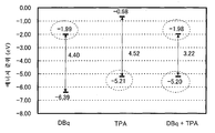
도 64에 도시한 바와 같이, DBq 및 TPA의 이량체는 TPA의 LUMO 준위보다 더 깊은(더 낮은) DBq의 LUMO 준위(-1.99 eV) 및 DBq의 HOMO 준위보다 더 얕은(더 높은) TPA의 HOMO 준위(-5.21 eV)의 영향하에서 DBq 및 TPA의 여기착물을 형성한다는 것을 시사한다. 사실상, 도 65ca 및 도 65cb로부터 명백한 바와 같이, DBq 및 TPA의 이량체의 LUMO는 DBq 측에 분포되며, 그의 HOMO는 TPA 측에 분포된다.As shown in FIG. 64, the dimer of DBq and TPA is HOMO of TPA deeper (lower) than the LUMO level of TPA (-1.99 eV) and shallower (higher) TPA of DBq than the HOMO level of DBq. It suggests that under the influence of the level (-5.21 eV), excitation complexes of DBq and TPA are formed. In fact, as apparent from Figs. 65ca and 65cb, the LUMO of the dimer of DBq and TPA is distributed on the DBq side, and its HOMO is distributed on the TPA side.
그 다음, DBq 단독의 S1 및 T1에서의 최적의 분자 구조로부터 얻은 여기 에너지를 나타낸다. 여기서, S1 및 T1 여기 에너지는 DBq 단독으로부터 얻은 각각의 형광 및 인광 파장에 해당한다. DBq 단독의 S1 여기 에너지는 3.294 eV이고, 형광 파장은 376.4 ㎚이다. DBq 단독의 T1 여기 에너지는 2.460 eV이고, 인광 파장은 504.1 ㎚이다.Then, the excitation energy obtained from the optimal molecular structure at S 1 and T 1 of DBq alone is shown. Here, S 1 and T 1 excitation energies correspond to respective fluorescence and phosphorescence wavelengths obtained from DBq alone. The S 1 excitation energy of DBq alone is 3.294 eV, and the fluorescence wavelength is 376.4 nm. The T 1 excitation energy of DBq alone is 2.460 eV, and the phosphorescence wavelength is 504.1 nm.
게다가, TPA 단독의 S1 및 T1의 최적의 분자 구조로부터 얻은 여기 에너지를 나타낸다. 여기서, S1 및 T1 여기 에너지는 TPA 단독으로부터 얻은 각각의 형광 및 인광 파장에 해당한다. TPA 단독의 S1 여기 에너지는 3.508 eV이고, 형광 파장은 353.4 ㎚이다. TPA 단독의 T1 여기 에너지는 2.610 eV이고, 인광 파장은 474.7 ㎚이다.Moreover, it shows the excitation energy obtained from the optimal molecular structure of S 1 and T 1 of TPA alone. Here, the S 1 and T 1 excitation energy corresponds to the respective fluorescence and phosphorescence wavelengths obtained from TPA alone. The S 1 excitation energy of TPA alone is 3.508 eV and the fluorescence wavelength is 353.4 nm. The T 1 excitation energy of TPA alone is 2.610 eV, and the phosphorescence wavelength is 474.7 nm.
더욱이, S1 및 T1에서 DBq 및 TPA의 이량체의 최적의 분자 구조로부터 얻은 여기 에너지를 나타낼 것이다. S1 및 T1 여기 에너지는 DBq 및 TPA의 이량체로부터 얻은 각각의 형광 및 인광 파장에 해당한다. DBq 및 TPA의 이량체의 S1 여기 에너지는 2.036 eV이고, 형광 파장은 609.1 ㎚이다. DBq 및 TPA의 이량체의 T1 여기 에너지는 2.030 eV이고, 인광 파장은 610.0 ㎚이다.Moreover, it will represent the excitation energy obtained from the optimal molecular structure of the dimer of DBq and TPA in S 1 and T 1 . The S 1 and T 1 excitation energies correspond to the respective fluorescence and phosphorescence wavelengths obtained from dimers of DBq and TPA. The S 1 excitation energy of the dimer of DBq and TPA is 2.036 eV, and the fluorescence wavelength is 609.1 nm. The T 1 excitation energy of the dimer of DBq and TPA is 2.030 eV, and the phosphorescence wavelength is 610.0 nm.
상기로부터 DBq 단독 및 TPA 단독의 각각의 인광 파장은 형광 파장에 대하여 약 100 ㎚ 정도로 더 긴 파장측으로 이동되는 것으로 밝혀졌다. 이러한 결과는 상기 기재된 CBP(측정값)와 유사한 경향을 나타내며, 계산의 타당성을 뒷받침한다.From the above, it has been found that the phosphorescence wavelengths of DBq alone and TPA alone are shifted to the longer wavelength side, about 100 nm relative to the fluorescence wavelength. These results show a trend similar to the CBP (measured value) described above, supporting the validity of the calculation.
다른 한편으로, DBq 및 TPA의 이량체의 형광 파장은 DBq 단독 및 TPA 단독의 형광 파장에 대하여 더 긴 파장측에 위치하는 것으로 밝혀졌다. 이러한 결과는 하기 기재된 실시예(측정값)와 유사한 경향을 나타내며, 계산의 타당성을 뒷받침한다. 또한, DBq 및 TPA의 이량체의 형광 파장 및 인광 파장 사이의 차이는 단지 0.9 ㎚이며, 이들 파장은 실질적으로 동일한 것으로 밝혀졌다.On the other hand, it was found that the fluorescence wavelengths of the dimers of DBq and TPA are located on the longer wavelength side with respect to the fluorescence wavelengths of DBq alone and TPA alone. These results show a similar trend to the examples described below (measured values) and support the validity of the calculation. In addition, the difference between the fluorescence wavelength and the phosphorescence wavelength of the dimer of DBq and TPA is only 0.9 nm, and these wavelengths have been found to be substantially the same.
이러한 결과는 여기착물이 일중항 여기 에너지 및 삼중항 여기 에너지를 실질적으로 동일한 에너지로 집약시킬 수 있다는 것을 나타낸다. 그러므로, 상기 기재한 바와 같이 여기착물은 그의 일중항 상태 및 삼중항 상태 모두로부터 인광 화합물에 대하여 효율적으로 에너지를 이동시킬 수 있다는 것을 나타낸다.These results indicate that the excitation complex can aggregate singlet excitation energy and triplet excitation energy to substantially the same energy. Therefore, as described above, it shows that the excitation complex can efficiently transfer energy to the phosphorescent compound from both its singlet state and triplet state.
그러한 효과는 에너지 이동에 대한 매체로서 여기착물의 사용에 대하여 특이적이다. 일반적으로, 호스트 물질의 일중항 여기 상태 또는 삼중항 여기 상태로부터 인광 화합물로의 에너지 이동을 고려한다. 다른 한편으로, 본 발명의 하나의 실시형태는 호스트 물질 및 또다른 물질의 여기착물(제1의 유기 화합물 및 제2의 유기 화합물의 여기착물)이 우선 형성되며, 여기착물로부터의 에너지 이동을 사용하는 통상의 기술과는 크게 상이하다. 게다가, 이러한 차이는 종래에는 없는 높은 발광 효율을 제공한다.Such effects are specific for the use of excitation complexes as a medium for energy transfer. In general, energy transfer from the singlet excited state or triplet excited state of the host material to the phosphorescent compound is considered. On the other hand, in one embodiment of the present invention, an excitation complex of a host material and another material (excitation complex of the first organic compound and the second organic compound) is first formed, and energy transfer from the excitation complex is used. It is greatly different from the conventional technology. Moreover, this difference provides a high luminous efficiency that is not conventional.
일반적으로, 발광 엘리먼트의 발광층에 대한 여기착물의 사용은 발광색을 제어할 수 있는 가치, 일반적으로 발광 효율에서의 상당한 감소를 야기하는 가치를 갖는다는 점에 유의한다. 그러므로, 여기착물의 사용은 매우 효율적인 발광 엘리먼트를 얻는데 적절하지 않은 것으로 고려된다. 그러나, 본 발명자들은 인광 화합물로의 에너지 이동을 위한 매체로서 여기착물의 사용이 본 발명의 하나의 실시형태에 제시된 바와 같이 발광 효율이, 반대로, 최대화될 수 있다는 것을 발견하였다. 이러한 기술적 개념은 통상의 고정 개념과는 상반되는 것이다.It is noted that, in general, the use of an excitation complex for the light emitting layer of the light emitting element has the value of controlling the emission color, and in general, causing a significant reduction in the light emission efficiency. Therefore, it is considered that the use of an excitation complex is not suitable for obtaining a highly efficient light emitting element. However, the present inventors have found that the use of excitation complexes as a medium for energy transfer to phosphorescent compounds can maximize luminescence efficiency, on the contrary, as presented in one embodiment of the present invention. This technical concept is contrary to the conventional fixed concept.
여기착물의 발광 스펙트럼 및 게스트 물질의 흡수 스펙트럼이 서로 충분하게 중첩되도록 하기 위하여, 발광 스펙트럼의 피크의 에너지 및 흡수 스펙트럼에서의 최저 에너지측에서의 흡수 밴드의 피크의 에너지 사이의 차이는 바람직하게는 0.3 eV 이하이다. 상기 차이는 더욱 바람직하게는 0.2 eV 이하, 더욱 더 바람직하게는 0.1 eV 이하이다.In order to ensure that the emission spectrum of the excitation complex and the absorption spectrum of the guest material overlap each other sufficiently, the difference between the energy of the peak of the emission spectrum and the energy of the absorption band peak at the lowest energy side in the absorption spectrum is preferably 0.3 eV or less to be. The difference is more preferably 0.2 eV or less, and even more preferably 0.1 eV or less.
게다가, 본 발명의 하나의 실시형태에서, 제1의 유기 화합물 또는 제2의 유기 화합물의 일중항 여기자로부터 여기착물이 형성된다.In addition, in one embodiment of the present invention, exciton complexes are formed from singlet excitons of the first organic compound or the second organic compound.
본 발명의 하나의 실시형태의 발광 엘리먼트에서, 여기착물 형성의 가능한 기본 과정은 제1의 및 제2의 유기 화합물 중 하나가 일중항 여기자를 형성한 후, 기저 상태의 다른 하나와 상호작용하는 것이다. 상기 기재한 바와 같이, 여기착물의 발광 스펙트럼 및 인광 화합물의 흡수 스펙트럼이 크게 중첩될 수 있어서, 에너지 이동 효율이 증가될 수 있다. 따라서, 외부 양자 효율이 높은 발광 엘리먼트를 얻을 수 있다.In the light emitting element of one embodiment of the present invention, a possible basic process of excitation complex formation is that one of the first and second organic compounds forms a singlet exciton and then interacts with the other in the ground state. . As described above, the emission spectrum of the excitation complex and the absorption spectrum of the phosphorescent compound can be largely overlapped, so that energy transfer efficiency can be increased. Therefore, a light emitting element with high external quantum efficiency can be obtained.
일중항 여기자는 상기 기재한 바와 같이 여기 수명이 짧다(τ가 작다). 그래서, 여기 에너지가 일중항 여기자로부터 게스트 물질로 이동되기 이전에 여기 에너지의 일부가 (발광 또는 열 불활성화를 통하여) 불활성화되는 문제가 있다(수학식 3에서 ΦET는 작아지는 경향이 있다). 그러나, 본 발명의 하나의 실시형태에서, 일중항 여기자는 여기착물을 신속하게 형성하므로 그러한 여기 에너지의 불활성화는 억제될 수 있다. 더욱이, 여기착물은 여기 수명이 비교적 길며, 이는 에너지 이동 효율 ΦET에 유리한 것으로 고려된다. 따라서, 엘리먼트의 효율뿐 아니라 그의 수명에 영향을 미칠 수 있는 호스트 물질의 일중항 여기 에너지의 불활성화는 본 발명의 하나의 실시형태의 적용에 의하여 억제될 수 있어서 수명이 긴 발광 엘리먼트를 얻을 수 있다.Singlet excitons have a short excitation lifetime (small τ) as described above. So, there is a problem that a part of the excitation energy is deactivated (via light emission or thermal inactivation) before the excitation energy is transferred from the singlet exciton to the guest material (in
본 발명의 하나의 실시형태에서, 여기착물의 여기 에너지는 인광 화합물로 충분히 이동되며 그리고 여기착물로부터의 발광은 실질적으로 관찰되지 않으므로 바람직하다. 그러므로, 여기착물을 통하여 인광 화합물로 에너지를 이동시켜 인광 화합물이 인광을 발광하는 것이 바람직하다.In one embodiment of the present invention, excitation energy of the excitation complex is sufficiently transferred to the phosphorescent compound, and luminescence from the excitation complex is preferable since it is substantially not observed. Therefore, it is preferable that the phosphorescent compound emits phosphorescence by transferring energy to the phosphorescent compound through the excitation complex.
상기 기재된 에너지 이동의 개념에 의하면, 본 발명의 하나의 실시형태는 제1의 및 제2의 유기 화합물 중 적어도 하나가 형광 화합물(즉, 일중항 여기 상태로부터 발광 또는 열 불활성이 발생되기 쉬운 화합물)인 경우 유효하다. 그러므로, 제1의 및 제2의 유기 화합물 중 적어도 하나는 형광 화합물인 것이 바람직하다.According to the concept of energy transfer described above, in one embodiment of the present invention, at least one of the first and second organic compounds is a fluorescent compound (i.e., a compound prone to luminescence or thermal inertness from singlet excited state) Is valid. Therefore, it is preferable that at least one of the first and second organic compounds is a fluorescent compound.
인광 화합물이 호스트 물질로서 작용하는 유기 화합물로서 사용되는 경우에서, 유기 화합물 그 자체는 발광되기 쉬우며, 에너지를 게스트 물질로 이동시키기는 곤란하다는 점에 유의한다. 이러한 경우에서, 유기 화합물이 효율적으로 발광될 수 있는 경우에는 이로우나, 호스트 물질로서 작용하는 유기 화합물이 농도 소광의 문제를 야기하므로 높은 발광 효율을 달성하기는 곤란하다. 이러한 이유로, 유기 화합물은 형광 화합물이 되며 그리고 상기 기재된 조성물을 사용하여 에너지 이동을 달성하는 것이 바람직하다.Note that in the case where the phosphorescent compound is used as an organic compound that acts as a host material, the organic compound itself is easy to emit light, and it is difficult to transfer energy to the guest material. In this case, it is advantageous if the organic compound can be efficiently emitted, but it is difficult to achieve high luminous efficiency since the organic compound serving as a host material causes a problem of concentration quenching. For this reason, the organic compound becomes a fluorescent compound and it is desirable to achieve energy transfer using the composition described above.
게다가, 본 발명의 하나의 실시형태에서, 인광 화합물은 유기금속 착물인 것이 바람직하다.Moreover, in one embodiment of the present invention, it is preferred that the phosphorescent compound is an organometallic complex.
본 발명의 하나의 실시형태에 사용된 여기착물을 하기에서 구체적으로 기재한다.The excitation complex used in one embodiment of the present invention is specifically described below.
<여기착물><Here complex>
여기착물(여기된 착물)은 여기 상태가 상이한 분자 사이의 상호작용에 의하여 형성된다. 여기착물은 일반적으로 비교적 깊은 LUMO 준위를 갖는 물질 및 비교적 얕은 HOMO 준위를 갖는 물질 사이에서 용이하게 형성되는 것으로 공지되어 있다.Excitation complexes (excited complexes) are formed by interactions between molecules with different excitation states. Excitation complexes are generally known to be readily formed between materials having a relatively deep LUMO level and materials having a relatively shallow HOMO level.
발광 파장은 HOMO 준위 및 LUMO 준위 사이의 에너지의 차이에 의존한다. 에너지 차이가 클 때, 발광 파장은 짧다. 에너지 차이가 작을 때, 발광 파장은 길다.The emission wavelength depends on the difference in energy between the HOMO level and the LUMO level. When the energy difference is large, the emission wavelength is short. When the energy difference is small, the emission wavelength is long.
여기서, 본 발명의 하나의 실시형태에 사용된 제1의 유기 화합물 및 제2의 유기 화합물의 HOMO 준위 및 LUMO 준위는 서로 상이하다. 구체적으로는, 에너지 준위는 제1의 유기 화합물의 HOMO 준위 < 제2의 유기 화합물의 HOMO 준위 < 제1의 유기 화합물의 LUMO 준위 < 제2의 유기 화합물의 LUMO 준위의 순서로 높다(도 17 참조).Here, the HOMO level and the LUMO level of the first organic compound and the second organic compound used in one embodiment of the present invention are different from each other. Specifically, the energy level is high in the order of HOMO level of the first organic compound <HOMO level of the second organic compound <LUMO level of the first organic compound <LUMO level of the second organic compound (see FIG. 17) ).
여기착물이 이들 2종의 유기 화합물에 의하여 형성될 때, 여기착물의 LUMO 준위 및 HOMO 준위는 각각 제1의 유기 화합물 및 제2의 유기 화합물로부터 유래한다(도 17 참조). 그러므로, 여기착물의 에너지 차이는 제1의 유기 화합물의 에너지 차이 및 제2의 유기 화합물의 에너지 차이보다 작다. 환언하면, 여기착물의 발광 파장은 제1의 유기 화합물 및 제2의 유기 화합물의 발광 파장보다 더 길다.When the excitation complex is formed by these two types of organic compounds, the LUMO level and the HOMO level of the excitation complex are derived from the first organic compound and the second organic compound, respectively (see FIG. 17). Therefore, the energy difference of the excitation complex is smaller than the energy difference of the first organic compound and the energy difference of the second organic compound. In other words, the emission wavelength of the excitation complex is longer than that of the first organic compound and the second organic compound.
본 발명의 하나의 실시형태에 사용된 여기착물의 형성 과정은 크게 2개의 과정으로 분류되는 것으로 고려된다.The formation process of the excitation complex used in one embodiment of the present invention is considered to be largely classified into two processes.
≪일렉트로플렉스≫≪Electroflex≫
본 명세서에서, 용어 "일렉트로플렉스"는 기저 상태의 제1의 유기 화합물 및 기저 상태의 제2의 유기 화합물이 여기착물을 직접 형성한다는 것을 의미한다.In the present specification, the term "electroflex" means that the first organic compound in the ground state and the second organic compound in the ground state directly form an excitation complex.
상기 기재한 바와 같이, 일반적으로 전자 및 정공이 호스트 물질 중에서 재결합될 때, 여기 에너지는 여기 상태의 호스트 물질로부터 게스트 물질로 이동되며, 게스트 물질은 여기 상태가 되어 발광된다.As described above, in general, when electrons and holes recombine in the host material, the excitation energy is transferred from the host material in the excited state to the guest material, and the guest material becomes excited and emits light.
이때, 여기 에너지가 호스트 물질로부터 게스트 물질로 이동되기 이전에, 호스트 물질 그 자체는 발광되거나 또는 여기 에너지는 열 에너지가 되며, 이는 여기 에너지의 부분 불활성화를 초래한다. 특히, 호스트 물질이 일중항 여기 상태에 있는 경우, 삼중항 여기 상태에 있는 경우보다 여기 수명이 더 짧으며, 이는 일중항 여기 에너지의 불활성화를 쉽게 초래한다. 여기 에너지의 불활성화는 발광 엘리먼트의 수명 감소의 원인 중 하나가 된다.At this time, before the excitation energy is transferred from the host material to the guest material, the host material itself emits light or the excitation energy becomes thermal energy, which results in partial deactivation of the excitation energy. In particular, when the host material is in the singlet excited state, the excitation life is shorter than in the triplet excited state, which easily leads to the deactivation of the singlet excited energy. Inactivation of excitation energy is one of the causes of reduction in the life of the light emitting element.
그러나, 본 발명의 하나의 실시형태에서, 일렉트로플렉스는 캐리어를 갖는 제1의 유기 화합물 및 제2의 유기 화합물(양이온 또는 음이온)로부터 형성되며; 그리하여 여기 수명이 짧은 일중항 여기자의 형성이 억제될 수 있다. 환언하면, 일중항 여기자의 형성 없이 여기착물이 직접 형성되는 과정이 될 수 있다. 그래서, 일중항 여기 에너지의 불활성화가 억제될 수 있다. 따라서, 수명이 긴 발광 엘리먼트를 얻을 수 있다.However, in one embodiment of the present invention, the electroflex is formed from a first organic compound having a carrier and a second organic compound (cation or anion); Thus, the formation of singlet excitons with a short excitation life can be suppressed. In other words, it can be a process in which excitation complexes are directly formed without the formation of singlet excitons. Thus, inactivation of singlet excitation energy can be suppressed. Therefore, it is possible to obtain a light emitting element having a long life.
예를 들면, 제1의 유기 화합물이 전자-포획 성질을 갖는 화합물이며 그리고 제2의 유기 화합물이 정공-포획 성질을 갖는 화합물인 경우에서, 일렉트로플렉스는 제1의 유기 화합물의 음이온 및 제2의 유기 화합물의 양이온으로부터 직접 형성된다. 이는 상기 기재된 방식으로 호스트 물질의 일중항 여기 상태의 생성을 억제하고 그리고 에너지를 일렉트로플렉스로부터 게스트 물질로 이동시켜 발광 효율이 높은 발광 엘리먼트를 얻는 신규한 개념이다. 호스트 물질의 삼중항 여기 상태의 생성은 유사하게 억제되며 그리고 일렉트로플렉스가 직접 형성되므로, 일렉트로플렉스로부터 게스트 물질로의 에너지 이동이 고려된다는 점에 유의한다. 이러한 메카니즘도 또한 신규하다.For example, in the case where the first organic compound is a compound having electron-capturing properties and the second organic compound is a compound having hole-capturing properties, the electroflex is an anion of the first organic compound and a second It is formed directly from cations of organic compounds. This is a novel concept that suppresses the generation of singlet excited states of the host material in the manner described above and transfers energy from the electroflex to the guest material to obtain a light emitting element with high luminous efficiency. Note that the generation of the triplet excited state of the host material is similarly inhibited and the electroflex is formed directly, so the energy transfer from the electroplex to the guest material is considered. This mechanism is also novel.
형성된 일렉트로플렉스의 발광 스펙트럼은 제1의 및 제2의 유기 화합물 각각의 발광 파장에 대하여 더 긴 파장측에 위치한다.The emission spectrum of the formed electroflex is located on the longer wavelength side for each of the emission wavelengths of the first and second organic compounds.
일렉트로플렉스의 발광 스펙트럼 및 인광 화합물의 흡수 스펙트럼 사이의 중첩은 제1의 유기 화합물(또는 제2의 유기 화합물)의 발광 스펙트럼 및 인광 화합물의 흡수 스펙트럼 사이의 중첩보다 더 크다. 본 발명의 하나의 실시형태의 발광 엘리먼트는 일렉트로플렉스의 발광 스펙트럼 및 인광 화합물의 흡수 스펙트럼 사이의 중첩을 이용하여 에너지를 이동시키며 그리하여 높은 에너지 이동 효율을 갖는다. 그러므로, 본 발명의 하나의 실시형태에서, 외부 양자 효율이 높은 발광 엘리먼트를 얻을 수 있다.The overlap between the emission spectrum of the electroplex and the absorption spectrum of the phosphorescent compound is greater than the overlap between the emission spectrum of the first organic compound (or the second organic compound) and the absorption spectrum of the phosphorescent compound. The light emitting element of one embodiment of the present invention transfers energy using the overlap between the emission spectrum of the electroflex and the absorption spectrum of the phosphorescent compound, and thus has a high energy transfer efficiency. Therefore, in one embodiment of the present invention, a light emitting element with high external quantum efficiency can be obtained.
≪여기자에 의한 여기착물의 형성≫≪Formation of excitation complex by here >>
또다른 과정으로서, 제1의 및 제2의 유기 화합물 중 하나가 일중항 여기자를 형성하여 기저 상태의 다른 하나와 상호작용하여 여기착물을 형성하는 기본 과정이 고려된다. 일렉트로플렉스와 달리, 제1의 유기 화합물 또는 제2의 유기 화합물의 일중항 여기 상태는 이 경우에서는 일시적으로 생성되지만, 이는 여기착물로 신속하게 전환되어 단일 여기 에너지의 불활성화를 억제할 수 있다. 그래서, 제1의 유기 화합물 또는 제2의 유기 화합물의 여기 에너지의 불활성화를 억제할 수 있다. 따라서, 본 발명의 하나의 실시형태에서, 수명이 긴 발광 엘리먼트를 얻을 수 있다. 호스트 물질의 삼중항 여기 상태는 또한 여기착물로 신속하게 전환되며, 여기착물로부터 게스트 물질로 에너지가 이동되는 것으로 고려되는 점에 유의한다.As another process, a basic process is considered in which one of the first and second organic compounds forms a singlet exciton and interacts with the other in the ground state to form an excitation complex. Unlike electroplexes, the singlet excited state of the first organic compound or the second organic compound is temporarily generated in this case, but it can be quickly converted into an excitation complex to suppress inactivation of a single excitation energy. Thus, inactivation of the excitation energy of the first organic compound or the second organic compound can be suppressed. Therefore, in one embodiment of the present invention, a light-emitting element having a long life can be obtained. Note that the triplet excitation state of the host material is also rapidly converted to the excitation complex, and it is considered that energy is transferred from the excitation complex to the guest material.
형성된 여기착물의 발광 스펙트럼은 제1의 및 제2의 유기 화합물의 각각의 발광 파장에 대하여 더 긴 파장측에 위치한다.The emission spectrum of the formed excitation complex is located on the longer wavelength side for each emission wavelength of the first and second organic compounds.
여기착물의 발광 스펙트럼 및 인광 화합물의 흡수 스펙트럼 사이의 중첩은 제1의 유기 화합물(또는 제2의 유기 화합물)의 발광 스펙트럼 및 인광 화합물의 흡수 스펙트럼 사이의 중첩보다 크다. 본 발명의 하나의 실시형태의 발광 엘리먼트는 여기착물의 발광 스펙트럼 및 인광 화합물의 흡수 스펙트럼 사이의 중첩을 사용하여 에너지를 이동시키며, 그리하여 에너지 이동 효율이 높다. 따라서, 본 발명의 하나의 실시형태에서, 외부 양자 효율이 높은 발광 엘리먼트를 얻을 수 있다.The overlap between the emission spectrum of the excitation complex and the absorption spectrum of the phosphorescent compound is greater than the overlap between the emission spectrum of the first organic compound (or the second organic compound) and the absorption spectrum of the phosphorescent compound. The light emitting element of one embodiment of the present invention transfers energy using the overlap between the emission spectrum of the excitation complex and the absorption spectrum of the phosphorescent compound, so that the energy transfer efficiency is high. Therefore, in one embodiment of the present invention, a light emitting element with high external quantum efficiency can be obtained.
예를 들면, 제1의 유기 화합물이 전자-포획 성질을 갖는 화합물이며, 제2의 유기 화합물은 정공-포획 성질을 갖는 화합물이며 그리고 이들 화합물의 HOMO 준위 사이의 차이 및 LUMO 준위 사이의 차이가 큰(구체적으로는, 0.3 eV 이상) 경우에서, 전자는 제1의 유기 화합물로 선택적으로 주입되며, 정공은 제2의 유기 화합물로 선택적으로 주입된다. 이러한 경우에서, 일중항 여기자를 통하여 여기착물이 형성되는 과정보다 일렉트로플렉스가 형성되는 과정이 우선하는 것으로 판단된다.For example, the first organic compound is a compound having electron-capturing properties, the second organic compound is a compound having hole-capturing properties, and the difference between the HOMO level and the LUMO level of these compounds is large. In the case (specifically, 0.3 eV or more), electrons are selectively injected into the first organic compound, and holes are selectively injected into the second organic compound. In this case, it is determined that the process of forming the electroplex takes priority over the process of forming the excitation complex through the singlet exciton.
이러한 실시형태는 임의의 기타의 실시형태와 적절하게 조합될 수 있다는 점에 유의한다.Note that this embodiment can be combined with any other embodiment as appropriate.
실시형태 2
본 실시형태에서, 본 발명의 하나의 실시형태의 발광 엘리먼트는 도 16a 내지 도 16c을 참조하여 기재한다In this embodiment, the light emitting element of one embodiment of the present invention is described with reference to Figs. 16A to 16C.
도 16a는 제1의 전극(103) 및 제2의 전극(108) 사이에 EL층(102)을 포함하는 발광 엘리먼트를 도시한다. 도 16a에서의 발광 엘리먼트는 제1의 전극(103)의 위에 정공 주입층(701), 정공 수송층(702), 발광층(703), 전자 수송층(704) 및 전자 주입층(705)의 순서로 적층되어 있으며, 그 위에 제2의 전극(108)이 제공된다.16A shows a light emitting element including an
제1의 전극(103)은 일 함수가 큰(구체적으로는, 4.0 eV 이상) 임의의 금속, 합금, 전도성 화합물, 그의 혼합물 등을 사용하여 형성되는 것이 바람직하다. 그의 구체적인 예로는 산화인듐-산화주석(ITO: 산화인듐주석), 규소 또는 산화규소를 함유하는 산화인듐-산화주석, 산화인듐-산화아연(산화인듐아연), 산화텅스텐 및 산화아연을 함유하는 산화인듐(IWZO) 등을 들 수 있다. 이들 전도성 금속 산화물의 필름은 일반적으로 스퍼터링 방법에 의하여 형성되지만, 졸-겔 방법 등의 적용에 의하여 형성될 수 있다. 예를 들면, 산화인듐-산화아연 필름은 산화아연을 산화인듐에 1 내지 20 중량%로 첨가한 타겟을 사용하는 스퍼터링 방법에 의하여 형성될 수 있다. 추가로, IWZO 필름은 산화텅스텐을 산화인듐에 0.5 내지 5 중량%로 첨가하고 그리고 산화아연을 산화인듐에 0.1 내지 1 중량%로 첨가하는 타겟을 사용하는 스퍼터링 방법에 의하여 형성될 수 있다. 기타의 예로는 그라펜, 금, 백금, 니켈, 텅스텐, 크롬, 몰리브덴, 철, 코발트, 구리, 팔라듐, 금속 물질의 질화물(예, 질화티탄) 등을 들 수 있다.It is preferable that the
EL층(102)에 포함되며 그리고 제1의 전극(103)과 접촉하여 형성된 층이 유기 화합물 및 전자 수용체(수용체)를 혼합하여 후술하는 복합 물질을 형성하는 경우, 제1의 전극(103)에 사용되는 물질로서 일 함수와는 무관하게 임의의 각종 금속, 합금, 전기 전도성 화합물, 그의 혼합물 등을 사용할 수 있으며; 예를 들면, 알루미늄, 은, 알루미늄을 포함하는 합금(예, Al-Si) 등도 또한 사용될 수 있다는 점에 유의한다.When the layer included in the
제1의 전극(103)은 예를 들면 스퍼터링 방법, 증착법(진공 증착법 포함) 등에 의하여 형성될 수 있다.The
제2의 전극(108)은 일 함수가 낮은(바람직하게는 3.8 eV 이하) 임의의 금속, 합금, 전기 전도성 화합물, 그의 혼합물 등을 사용하여 형성되는 것이 바람직하다. 그의 구체적인 예로는 원소주기율표의 1족 및 2족에 속하는 원소, 즉 리튬 및 세슘 등의 알칼리 금속, 칼슘 및 스트론튬, 마그네슘 등의 알칼리 토금속, 그의 합금(예, Mg-Ag 및 Al-Li), 유로퓸 및 이테르븀 등의 희토류 금속, 그의 합금, 알루미늄, 은 등을 들 수 있다.It is preferred that the
유기 화합물 및 전자 공여체(공여체)를 혼합하여 형성된 후술하는 복합 물질을 사용하여 EL층(102)에 포함되며 그리고 제2의 전극(108)과 접촉되어 형성된 층을 형성할 때, Al, Ag, ITO 및, 규소 또는 산화규소를 함유하는 산화인듐-산화주석 등의 임의의 각종 전도성 물질은 일 함수와 상관 없이 사용될 수 있다.When forming a layer included in the
제2의 전극(108)이 형성될 때, 진공 증착법 또는 스퍼터링 방법이 사용될 수 있다는 점에 유의한다. 은 페이스트 등을 사용하는 경우에서, 코팅 방법, 잉크젯 방법 등을 사용할 수 있다.Note that when the
EL층(102)은 적어도 발광층(703)을 포함한다. EL층(102)의 일부의 경우, 공지의 물질을 사용할 수 있으며, 저 분자계 화합물 또는 고분자계 화합물을 사용할 수 있다. EL층(102)을 형성하는 물질은 유기 화합물로 이루어질 수 있거나 또는 무기 화합물을 일부로서 포함할 수 있다는 점에 유의한다.The
추가로, 도 16a에 도시한 바와 같이, EL층(102)은 발광층(703)뿐 아니라, 정공 주입 성질이 높은 물질을 포함하는 정공 주입층(701), 정공 수송 성질이 높은 물질을 포함하는 정공 수송층(702), 전자 수송 성질이 높은 물질을 포함하는 전자 수송층(704), 전자 주입 성질이 높은 물질을 포함하는 전자 주입층(705) 등의 층의 적절한 조합을 포함한다.In addition, as shown in FIG. 16A, the
정공 주입층(701)은 정공 주입 성질이 높은 물질을 함유하는 층이다. 정공 주입 성질이 높은 물질로서, 산화몰리브덴, 산화티탄, 산화바나듐, 산화레늄, 산화루테늄, 산화크롬, 산화지르코늄, 산화하프늄, 산화탄탈륨, 산화은, 산화텅스텐 또는 산화망간 등의 금속 산화물을 사용할 수 있다. 대안으로, 프탈로시아닌(약어: H2Pc) 또는 구리(II) 프탈로시아닌(약어: CuPc) 등의 프탈로시아닌계 화합물을 사용할 수 있다.The
사용할 수 있는 물질의 기타예로는 4,4',4"-트리스(N,N-디페닐아미노)트리페닐아민(약어: TDATA), 4,4',4"-트리스[N-(3-메틸페닐)-N-페닐아미노]트리페닐아민(약어: MTDATA), 4,4'-비스[N-(4-디페닐아미노페닐)-N-페닐아미노]비페닐(약어: DPAB), 4,4'-비스(N-{4-[N'-(3-메틸페닐)-N'-페닐아미노]페닐}-N-페닐아미노)비페닐(약어: DNTPD), 1,3,5-트리스[N-(4-디페닐아미노페닐)-N-페닐아미노]벤젠(약어: DPA3B), 3-[N-(9-페닐카르바졸-3-일)-N-페닐아미노]-9-페닐카르바졸(약어: PCzPCA1), 3,6-비스[N-(9-페닐카르바졸-3-일)-N-페닐아미노]-9-페닐카르바졸(약어: PCzPCA2) 및 3-[N-(1-나프틸)-N-(9-페닐카르바졸-3-일)아미노]-9-페닐카르바졸(약어: PCzPCN1) 등의 저 분자 유기 화합물인 방향족 아민 화합물 등을 들 수 있다.Other examples of materials that can be used are 4,4 ', 4 "-tris (N, N-diphenylamino) triphenylamine (abbreviation: TDATA), 4,4', 4" -tris [N- (3 -Methylphenyl) -N-phenylamino] triphenylamine (abbreviation: MTDATA), 4,4'-bis [N- (4-diphenylaminophenyl) -N-phenylamino] biphenyl (abbreviation: DPAB), 4 , 4'-bis (N- {4- [N '-(3-methylphenyl) -N'-phenylamino] phenyl} -N-phenylamino) biphenyl (abbreviation: DNTPD), 1,3,5-tris [N- (4-diphenylaminophenyl) -N-phenylamino] benzene (abbreviation: DPA3B), 3- [N- (9-phenylcarbazol-3-yl) -N-phenylamino] -9-phenyl Carbazole (abbreviation: PCzPCA1), 3,6-bis [N- (9-phenylcarbazole-3-yl) -N-phenylamino] -9-phenylcarbazole (abbreviation: PCzPCA2) and 3- [N- And aromatic amine compounds that are low molecular organic compounds such as (1-naphthyl) -N- (9-phenylcarbazole-3-yl) amino] -9-phenylcarbazole (abbreviation: PCzPCN1).
사용할 수 있는 물질의 기타의 예로는 폴리(N-비닐카르바졸)(약어: PVK), 폴리(4-비닐트리페닐아민)(약어: PVTPA), 폴리[N-(4-{N'-[4-(4-디페닐아미노)페닐]페닐-N'-페닐아미노}페닐)메타크릴아미드](약어: PTPDMA) 및 폴리[N,N'-비스(4-부틸페닐)-N,N'-비스(페닐)벤지딘](약어: 폴리-TPD) 등의 고 분자 화합물(예, 올리고머, 덴드리머 및 중합체) 및, 폴리(3,4-에틸렌디옥시티오펜)/폴리(스티렌술폰산)(PEDOT/PSS) 및 폴리아닐린/폴리(스티렌술폰산)(PAni/PSS) 등의 산을 첨가한 고 분자 화합물을 들 수 있다.Other examples of materials that can be used are poly (N-vinylcarbazole) (abbreviation: PVK), poly (4-vinyltriphenylamine) (abbreviation: PVTPA), poly [N- (4- {N '-[ 4- (4-diphenylamino) phenyl] phenyl-N'-phenylamino} phenyl) methacrylamide] (abbreviation: PTPDMA) and poly [N, N'-bis (4-butylphenyl) -N, N ' High molecular compounds such as bis (phenyl) benzidine] (abbreviation: poly-TPD) (eg, oligomers, dendrimers and polymers), and poly (3,4-ethylenedioxythiophene) / poly (styrenesulfonic acid) (PEDOT / PSS) and polyaniline / poly (styrenesulfonic acid) (PAni / PSS).
정공 주입층(701)의 경우, 유기 화합물 및 전자 수용체(수용체)를 혼합하여 형성된 복합 물질을 사용할 수 있다. 전자 수용체에 의하여 유기 화합물 중에서 정공이 생성되는 상기 복합 물질은 정공 주입 및 정공 수송 성질이 크다. 이러한 경우에서, 유기 화합물은 생성된 정공을 수송하는데 있어서 우수한 물질(정공 수송 성질이 높은 물질)이 바람직하다.In the case of the
복합 물질에 사용되는 유기 화합물의 예로는 방향족 아민 화합물, 카르바졸 유도체, 방향족 탄화수소 및 고 분자 화합물(예, 올리고머, 덴드리머 및 중합체) 등의 각종 화합물을 들 수 있다. 복합 물질에 사용되는 유기 화합물은 정공 수송 성질이 높은 유기 화합물이 바람직하며, 구체적으로는 10-6 ㎠/Vs 이상의 정공 이동도를 갖는 물질이 바람직하다. 상기 물질 이외에, 전자보다 정공의 수송성이 큰 임의의 물질을 사용할 수 있다는 점에 유의한다. 복합 물질에 사용될 수 있는 유기 화합물은 하기에 구체적으로 기재한다.Examples of the organic compound used in the composite material include various compounds such as aromatic amine compounds, carbazole derivatives, aromatic hydrocarbons and high molecular compounds (eg, oligomers, dendrimers and polymers). The organic compound used in the composite material is preferably an organic compound having high hole transport properties, specifically, a material having a hole mobility of 10 -6
복합 물질에 사용될 수 있는 유기 화합물의 예로는 TDATA, MTDATA, DPAB, DNTPD, DPA3B, PCzPCA1, PCzPCA2, PCzPCN1, 4,4'-비스[N-(1-나프틸)-N-페닐아미노]비페닐(약어: NPB 또는 α-NPD), N,N'-비스(3-메틸페닐)-N,N'-디페닐-[1,1'-비페닐]-4,4'-디아민(약어: TPD) 및 4-페닐-4'-(9-페닐플루오렌-9-일)트리페닐아민(약어: BPAFLP) 등의 방향족 아민 화합물 및, 4,4'-디(N-카르바졸릴)비페닐(약어: CBP), 1,3,5-트리스[4-(N-카르바졸릴)페닐]벤젠(약어: TCPB), 9-[4-(N-카르바졸릴)페닐]-10-페닐안트라센(약어: CzPA), 9-페닐-3-[4-(10-페닐-9-안트릴)페닐]-9H-카르바졸(약어: PCzPA) 및 1,4-비스[4-(N-카르바졸릴)페닐]-2,3,5,6-테트라페닐벤젠 등의 카르바졸 유도체를 들 수 있다.Examples of organic compounds that can be used in the composite material are TDATA, MTDATA, DPAB, DNTPD, DPA3B, PCzPCA1, PCzPCA2, PCzPCN1, 4,4'-bis [N- (1-naphthyl) -N-phenylamino] biphenyl (Abbreviation: NPB or α-NPD), N, N'-bis (3-methylphenyl) -N, N'-diphenyl- [1,1'-biphenyl] -4,4'-diamine (abbreviation: TPD ) And 4-phenyl-4 '-(9-phenylfluoren-9-yl) triphenylamine (abbreviation: BPAFLP), aromatic amine compounds, and 4,4'-di (N-carbazolyl) biphenyl (Abbreviation: CBP), 1,3,5-tris [4- (N-carbazolyl) phenyl] benzene (abbreviation: TCPB), 9- [4- (N-carbazolyl) phenyl] -10-phenyl Anthracene (abbreviation: CzPA), 9-phenyl-3- [4- (10-phenyl-9-anthryl) phenyl] -9H-carbazole (abbreviation: PCzPA) and 1,4-bis [4- (N- And carbazole derivatives such as carbazolyl) phenyl] -2,3,5,6-tetraphenylbenzene.
사용할 수 있는 유기 화합물의 기타의 예로는 2-tert-부틸-9,10-디(2-나프틸)안트라센(약어: t-BuDNA), 2-tert-부틸-9,10-디(1-나프틸)안트라센, 9,10-비스(3,5-디페닐페닐)안트라센(약어: DPPA), 2-tert-부틸-9,10-비스(4-페닐페닐)안트라센(약어: t-BuDBA), 9,10-디(2-나프틸)안트라센(약어: DNA), 9,10-디페닐안트라센(약어: DPAnth), 2-tert-부틸안트라센(약어: t-BuAnth), 9,10-비스(4-메틸-1-나프틸)안트라센(약어: DMNA), 9,10-비스[2-(1-나프틸)페닐]-2-tert-부틸안트라센, 9,10-비스[2-(1-나프틸)페닐]안트라센 및 2,3,6,7-테트라메틸-9,10-디(1-나프틸)안트라센 등의 방향족 탄화수소 화합물을 들 수 있다.Other examples of the organic compound that can be used are 2-tert-butyl-9,10-di (2-naphthyl) anthracene (abbreviation: t-BuDNA), 2-tert-butyl-9,10-di (1- Naphthyl) anthracene, 9,10-bis (3,5-diphenylphenyl) anthracene (abbreviation: DPPA), 2-tert-butyl-9,10-bis (4-phenylphenyl) anthracene (abbreviation: t-BuDBA ), 9,10-di (2-naphthyl) anthracene (abbreviation: DNA), 9,10-diphenylanthracene (abbreviation: DPAnth), 2-tert-butylanthracene (abbreviation: t-BuAnth), 9,10 -Bis (4-methyl-1-naphthyl) anthracene (abbreviation: DMNA), 9,10-bis [2- (1-naphthyl) phenyl] -2-tert-butylanthracene, 9,10-bis [2 Aromatic hydrocarbon compounds such as-(1-naphthyl) phenyl] anthracene and 2,3,6,7-tetramethyl-9,10-di (1-naphthyl) anthracene.
사용할 수 있는 유기 화합물의 기타의 예로는 2,3,6,7-테트라메틸-9,10-디(2-나프틸)안트라센, 9,9'-비안트릴, 10,10'-디페닐-9,9'-비안트릴, 10,10'-비스(2-페닐페닐)-9,9'-비안트릴, 10,10'-비스[(2,3,4,5,6-펜타페닐)페닐]-9,9'-비안트릴, 안트라센, 테트라센, 루브렌, 페릴렌, 2,5,8,11-테트라(tert-부틸)페릴렌, 펜타센, 코로넨, 4,4'-비스(2,2-디페닐비닐)비페닐(약어: DPVBi) 및 9,10-비스[4-(2,2-디페닐비닐)페닐]안트라센(약어: DPVPA) 등의 방향족 탄화수소 화합물을 들 수 있다Other examples of the organic compounds that can be used are 2,3,6,7-tetramethyl-9,10-di (2-naphthyl) anthracene, 9,9'-bianthryl, 10,10'-diphenyl- 9,9'-Bianthryl, 10,10'-bis (2-phenylphenyl) -9,9'-Bianthryl, 10,10'-bis [(2,3,4,5,6-pentaphenyl) Phenyl] -9,9'-bianthryl, anthracene, tetracene, rubrene, perylene, 2,5,8,11-tetra (tert-butyl) perylene, pentacene, coronene, 4,4'- Aromatic hydrocarbon compounds such as bis (2,2-diphenylvinyl) biphenyl (abbreviation: DPVBi) and 9,10-bis [4- (2,2-diphenylvinyl) phenyl] anthracene (abbreviation: DPVPA) Can
추가로, 전자 수용체의 예로는 7,7,8,8-테트라시아노-2,3,5,6-테트라플루오로퀴노디메탄(약어: F4-TCNQ) 및 클로라닐 등의 유기 화합물, 전이 금속의 산화물, 원소주기율표의 4족 내지 8족에 속하는 금속의 산화물 등을 들 수 있다. 구체적으로는, 산화바나듐, 산화니오븀, 산화탄탈륨, 산화크롬, 산화몰리브덴, 산화텅스텐, 산화망간 및 산화레늄은 그의 높은 전자-수용 성질로 인하여 바람직하다. 이들 중에서, 산화몰리브덴은 공기 중에서 안정하고, 흡습성이 낮으며, 취급이 용이하여 특히 바람직하다.Further, examples of the electron acceptor include organic compounds such as 7,7,8,8-tetracyano-2,3,5,6-tetrafluoroquinodimethane (abbreviation: F 4 -TCNQ) and chloranyl, Oxides of transition metals, oxides of metals belonging to
복합 물질은 상기 기재된 전자 수용체 및, PVK, PVTPA, PTPDMA 또는 폴리-TPD 등의 상기 기재된 고 분자 화합물을 사용하여 형성될 수 있으며, 정공 주입층(701)에 사용될 수 있다.The composite material can be formed using the electron acceptor described above and the high molecular compounds described above such as PVK, PVTPA, PTPDMA or poly-TPD, and can be used in the
정공 수송층(702)은 정공 수송 성질이 높은 물질을 함유하는 층이다. 정공 수송 성질이 높은 물질의 예로는 NPB, TPD, BPAFLP, 4,4'-비스[N-(9,9-디메틸플루오렌-2-일)-N-페닐아미노]비페닐(약어: DFLDPBi) 및 4,4'-비스[N-(스피로-9,9'-비플루오렌-2-일)-N-페닐아미노]비페닐(약어: BSPB) 등의 방향족 아민 화합물을 들 수 있다. 여기서 언급한 물질은 주로 정공 이동도가 10-6 ㎠/Vs 이상인 물질이다. 상기 물질 이외에, 전자보다 정공의 수송성이 큰 임의의 물질을 사용할 수 있다는 점에 유의한다. 정공 수송 성질이 높은 물질을 함유하는 층은 단일층에 한정되지 않으며, 그리고 임의의 상기 물질을 함유하는 2개 이상의 층의 적층체일 수 있다는 점에 유의한다.The
정공 수송층(702)의 경우, CBP, CzPA 또는 PCzPA 등의 카르바졸 유도체 또는 t-BuDNA, DNA 또는 DPAnth 등의 안트라센 유도체를 사용할 수 있다.For the
정공 수송층(702)의 경우, PVK, PVTPA, PTPDMA 또는 폴리-TPD 등의 고 분자 화합물을 또한 사용할 수 있다.For the
발광층(703)은 발광 물질을 함유하는 층이다. 본 실시형태의 발광층(703)은 인광 화합물, 제1의 유기 화합물 및 제2의 유기 화합물을 함유한다. 인광 화합물은 발광 물질(게스트 물질)이다. 제1의 및 제2의 유기 화합물 중 하나가 발광층(703)에서 다른 하나보다 함유량이 더 높은 것이 호스트 물질이다. 구체적으로 실시형태 1을 참조할 수 있다.The
인광 화합물로서, 유기금속 착물이 바람직하며, 특히 이리듐 착물이 바람직하다. 상기 기재한 포스터 메카니즘으로 인한 에너지 이동을 고려하면, 최장 파장측에 위치하는 인광 화합물의 흡수 밴드의 몰 흡광 계수는 바람직하게는 2,000 M-1·㎝-1 이상, 더욱 바람직하게는 5,000 M-1·㎝-1 이상이다. 몰 흡광 계수가 높은 화합물의 예로는 비스(3,5-디메틸-2-페닐피라지나토)(디피발로일메타나토)이리듐(III)(약어: [Ir(mppr-Me)2(dpm)]), (아세틸아세토나토)비스(4,6-디페닐피리미디나토)이리듐(III)(약어: [Ir(dppm)2(acac)]), 비스(2,3,5-트리페닐피라지나토)(디피발로일메타나토)이리듐(III)(약어: [Ir(tppr)2(dpm)]), (아세틸아세토나토)비스(6-메틸-4-페닐피리미디나토)이리듐(III)(약어: [Ir(mppm)2(acac)]), (아세틸아세토나토)비스(6-tert-부틸-4-페닐피리미디나토)이리듐(III)(약어: [Ir(tBuppm)2(acac)]) 등을 들 수 있다. 특히, [Ir(dppm)2(acac)] 등의 몰 흡광 계수가 5,000 M-1·㎝-1 이상인 물질을 사용할 경우, 약 30%의 외부 양자 효율을 달성할 수 있는 발광 엘리먼트를 얻을 수 있다.As the phosphorescent compound, an organometallic complex is preferred, and an iridium complex is particularly preferred. Considering the energy transfer due to the above-described poster mechanism, the molar extinction coefficient of the absorption band of the phosphorescent compound located on the longest wavelength side is preferably 2,000 M -1 · cm -1 or more, more preferably 5,000 M -1・ Cm -1 or more. Examples of compounds having a high molar extinction coefficient include bis (3,5-dimethyl-2-phenylpyrazinato) (dipivaloylmethanato) iridium (III) (abbreviation: [Ir (mppr-Me) 2 (dpm)] ), (Acetylacetonato) bis (4,6-diphenylpyrimidinato) iridium (III) (abbreviation: [Ir (dppm) 2 (acac)]), bis (2,3,5-triphenylpyrazina) Sat) (dipivaloylmethanato) iridium (III) (abbreviation: [Ir (tppr) 2 (dpm)]), (acetylacetonato) bis (6-methyl-4-phenylpyrimidinato) iridium (III) (Abbreviation: [Ir (mppm) 2 (acac)]), (acetylacetonato) bis (6-tert-butyl-4-phenylpyrimidinato) iridium (III) (abbreviation: [Ir (tBuppm) 2 (acac )]) And the like. In particular, when using a material having a molar extinction coefficient of 5,000 M -1 · cm -1 or more such as [Ir (dppm) 2 (acac)], a light emitting element capable of achieving an external quantum efficiency of about 30% can be obtained. .
제1의 유기 화합물 및 제2의 유기 화합물은 바람직하게는 예를 들면 2-[3-(디벤조티오펜-4-일)페닐]디벤조[f,h]퀴녹살린(약어: 2mDBTPDBq-II), 2-[4-(3,6-디페닐-9H-카르바졸-9-일)페닐]디벤조[f,h]퀴녹살린(약어: 2CzPDBq-III), 7-[3-(디벤조티오펜-4-일)페닐]디벤조[f,h]퀴녹살린(약어: 7mDBTPDBq-II), 6-[3-(디벤조티오펜-4-일)페닐]디벤조[f,h]퀴녹살린(약어: 6mDBTPDBq-II) 및 2-[4-(디벤조티오펜-4-일)페닐]-1-페닐-1H-벤즈이미다졸(약어: DBTBIm-II) 등의 전자를 수용하기 쉬운 화합물 중 임의의 하나(통상적으로 헤테로방향족 화합물) 및, 4,4'-비스[N-(1-나프틸)-N-페닐아미노]비페닐(약어: NPB 또는 α-NPD), 4-페닐-4'-(9-페닐-9H-카르바졸-3-일)트리페닐아민(약어: PCBA1BP), 4,4'-디(1-나프틸)-4"-(9-페닐-9H-카르바졸-3-일)트리페닐아민(약어: PCBNBB), 4-(1-나프틸)-4'-페닐트리페닐아민(약어: αNBA1BP), 2,7-비스[N-(4-디페닐아미노페닐)-N-페닐아미노]-스피로-9,9'-비플루오렌(약어: DPA2SF), 4,4',4"-트리스[N-(1-나프틸)-N-페닐아미노]트리페닐아민(약어: 1'-TNATA) 및 9-페닐-9H-3-(9-페닐-9H-카르바졸-3-일)카르바졸(약어: PCCP) 등의 정공을 수용하기 쉬운 화합물 중 임의의 하나(통상적으로 방향족 아민 화합물 및 카르바졸 화합물)의 조합이다. 상기 조성물을 사용하면, 여기착물로부터의 에너지 이동에 의하여서 뿐 아니라, 발광층에서 정공 수송 및 전자 수송 사이의 캐리어 균형의 조절에 의하여 발광 효율 및 수명의 개선 효과를 얻을 수 있다. 조합이 여기착물을 형성할 수 있는 한 본 발명은 이들 화합물에 한정되지 않는다는 점에 유의한다.The first organic compound and the second organic compound are preferably, for example, 2- [3- (dibenzothiophen-4-yl) phenyl] dibenzo [ f, h ] quinoxaline (abbreviation: 2mDBTPDBq-II ), 2- [4- (3,6-diphenyl-9H-carbazole-9-yl) phenyl] dibenzo [ f, h ] quinoxaline (abbreviation: 2CzPDBq-III), 7- [3- (di Benzothiophen-4-yl) phenyl] dibenzo [ f, h ] quinoxaline (abbreviation: 7mDBTPDBq-II), 6- [3- (dibenzothiophen-4-yl) phenyl] dibenzo [ f, h ] Accepts electrons such as quinoxaline (abbreviation: 6mDBTPDBq-II) and 2- [4- (dibenzothiophen-4-yl) phenyl] -1-phenyl-1H-benzimidazole (abbreviation: DBTBIm-II) Any one of the compounds easy to do (usually a heteroaromatic compound) and 4,4'-bis [N- (1-naphthyl) -N-phenylamino] biphenyl (abbreviation: NPB or α-NPD), 4 -Phenyl-4 '-(9-phenyl-9H-carbazol-3-yl) triphenylamine (abbreviation: PCBA1BP), 4,4'-di (1-naphthyl) -4 "-(9-phenyl- 9H-carbazol-3-yl) triphenylamine (abbreviation: PCBNBB), 4- (1-naphthyl) -4'-phenyltriphenylamine (abbreviation: αNBA1BP), 2,7-ratio [N- (4-diphenylaminophenyl) -N-phenylamino] -spiro-9,9'-bifluorene (abbreviation: DPA2SF), 4,4 ', 4 "-tris [N- (1-naph Tyl) -N-phenylamino] triphenylamine (abbreviation: 1'-TNATA) and 9-phenyl-9H-3- (9-phenyl-9H-carbazol-3-yl) carbazole (abbreviation: PCCP), etc. It is a combination of any one of compounds (usually aromatic amine compounds and carbazole compounds) that are easy to accept the holes of. When the composition is used, an effect of improving luminous efficiency and lifetime can be obtained not only by energy transfer from the excitation complex, but also by controlling the carrier balance between hole transport and electron transport in the light emitting layer. Note that the present invention is not limited to these compounds as long as the combination can form an excitation complex.
여기착물은 2개의 층 사이의 계면에서 형성될 수 있다는 점에 유의한다. 예를 들면, 제2의 유기 화합물을 함유하는 층 및 제1의 유기 화합물을 함유하는 층을 적층시킬 경우, 여기착물은 그의 계면 부근에서 형성된다. 이들 2개의 층은 본 발명의 하나의 실시형태에서 발광층으로서 사용될 수 있다. 그러한 경우에서, 인광 화합물은 계면의 부근에서 첨가된다. 인광 화합물은 2개의 층 중 하나 또는 둘다에 첨가될 수 있다.Note that the excitation complex can be formed at the interface between the two layers. For example, when laminating a layer containing a second organic compound and a layer containing a first organic compound, an excitation complex is formed near its interface. These two layers can be used as a light emitting layer in one embodiment of the present invention. In such a case, a phosphorescent compound is added in the vicinity of the interface. Phosphorescent compounds can be added to either or both layers.
전자 수송층(704)은 전자 수송 성질이 높은 물질을 함유하는 층이다. 전자 수송 성질이 큰 물질의 예로는 Alq3, 트리스(4-메틸-8-퀴놀리놀라토)알루미늄(약어: Almq3), 비스(10-히드록시벤조[h]퀴놀리나토)베릴륨(약어: BeBq2), BAlq, Zn(BOX)2 및 비스[2-(2-히드록시페닐)벤조티아졸라토]아연(약어: Zn(BTZ)2) 등의 금속 착물을 들 수 있다. 그의 기타의 예로는 2-(4-비페닐릴)-5-(4-tert-부틸페닐)-1,3,4-옥사디아졸(약어: PBD), 1,3-비스[5-(p-tert-부틸페닐)-1,3,4-옥사디아졸-2-일]벤젠(약어: OXD-7), 3-(4-tert-부틸페닐)-4-페닐-5-(4-비페닐릴)-1,2,4-트리아졸(약어: TAZ), 3-(4-tert-부틸페닐)-4-(4-에틸페닐)-5-(4-비페닐릴)-1,2,4-트리아졸(약어: p-EtTAZ), 바토페난트롤린(약어: BPhen), 바토쿠프로인(약어: BCP), 4,4'-비스(5-메틸벤족사졸-2-일)스틸벤(약어: BzOs) 등의 헤테로방향족 화합물을 들 수 있다. 여전히 기타의 예로는 폴리(2,5-피리딘-디일)(약어: PPy), 폴리[(9,9-디헥실플루오렌-2,7-디일)-co-(피리딘-3,5-디일)](약어: PF-Py) 및 폴리[(9,9-디옥틸플루오렌-2,7-디일)-co-(2,2'-비피리딘-6,6'-디일)](약어: PF-BPy) 등의 고 분자 화합물을 들 수 있다. 여기서 언급된 물질은 주로 전자 이동도가 10-6 ㎠/Vs 이상인 물질이다. 상기 물질 이외에, 정공보다 전자의 수송성이 큰 임의의 물질을 전자 수송층에 사용할 수 있다는 점에 유의한다.The
추가로, 전자 수송층은 단일층으로 한정되지 않으며, 임의의 상기 물질을 함유하는 2개 이상의 층의 적층체일 수 있다.Additionally, the electron transport layer is not limited to a single layer, and may be a laminate of two or more layers containing any of the above materials.
전자 주입층(705)은 전자 주입 성질이 높은 물질을 함유하는 층이다. 전자 주입층(705)에 사용될 수 있는 물질의 예로는 리튬, 세슘, 칼슘, 불소화리튬, 불소화세슘, 불소화칼슘 및 산화리튬 등의 알칼리 금속, 알칼리 토금속 및 그의 화합물, 불소화에르븀 등의 희토류 금속 화합물 및 전자 수송층(704)에 사용되는 전술한 물질을 들 수 있다.The
대안으로, 유기 화합물 및 전자 공여체(공여체)를 혼합하여 형성된 복합 물질은 전자 주입층(705)에 사용될 수 있다. 그러한 복합 물질은 전자 공여체에 의하여 유기 화합물에 전자가 생성되므로 전자 주입성 및 전자 수송성이 높다. 여기서 유기 화합물은 생성된 전자의 수송이 우수한 물질인 것이 바람직하며, 구체적으로 전자 수송층(704)을 위한 임의의 상기 물질(금속 착물 및 헤테로방향족 화합물 등)을 사용할 수 있다. 전자 공여체로서, 유기 화합물에 대한 전자-공여 성질을 나타내는 물질을 사용할 수 있다. 전자 공여체의 바람직한 구체적인 예로는 리튬, 세슘, 마그네슘, 칼슘, 에르븀 및 이테르븀 등의 알칼리 금속, 알칼리 토금속 및 희토류 금속을 들 수 있다. 임의의 알칼리 금속 산화물 및 알칼리 토금속 산화물이 바람직하며, 그의 예로는 산화리튬, 산화칼슘, 산화바륨 등 및 산화마그네슘 등의 루이스 염기 또는 테트라티아풀발렌(약어: TTF) 등의 유기 화합물을 사용할 수 있다.Alternatively, a composite material formed by mixing an organic compound and an electron donor (donor) can be used for the
상기 언급한 정공 주입층(701), 정공 수송층(702), 발광층(703), 전자 수송층(704) 및 전자 주입층(705)은 각각 증착법(진공 증착법 포함), 잉크젯 방법 또는 코팅 방법 등의 방법에 의하여 형성될 수 있다는 점에 유의한다.The above-mentioned
복수의 EL층은 도 16b에 도시한 바와 같이 제1의 전극(103) 및 제2의 전극(108) 사이에서 적층될 수 있다. 그러한 경우에서, 전하 발생층(803)은 적층되어 있는 제1의 EL층(800) 및 제2의 EL층(801) 사이에 제공되는 것이 바람직하다. 전하 발생층(803)은 상기 기재된 복합 물질을 사용하여 형성될 수 있다. 추가로, 전하 발생층(803)은 복합 물질을 함유하는 층 및 또다른 물질을 함유하는 층을 포함하는 적층된 구조를 가질 수 있다. 그러한 경우에서, 또다른 물질을 함유하는 층으로서, 전자-공여 물질 및 전자 수송 성질이 높은 물질을 함유하는 층, 투명한 전도성 필름으로 형성된 층 등을 사용할 수 있다. 상기 구조를 갖는 발광 엘리먼트의 경우, 에너지 이동 및 소광 등의 문제가 발생하기 어려우며, 물질 선택의 폭이 넓어서 높은 발광 효율 및 긴 수명 모두를 갖는 발광 엘리먼트를 용이하게 얻을 수 있다. 게다가, EL층 중 하나로부터의 인광 및 EL 층 중 다른 하나로부터의 형광을 제공하는 발광 엘리먼트를 용이하게 얻을 수 있다. 이러한 구조는 EL층의 임의의 상기 기재된 구조와 조합될 수 있다.The plurality of EL layers may be stacked between the
더욱이, EL층의 발광 색상을 상이하게 함으로써 발광 엘리먼트로부터 전체로서 소정의 색상의 광을 얻을 수 있다. 예를 들면, 2개의 EL층을 갖는 발광 엘리먼트에서 제1의 및 제2의 EL층의 발광 색상은 보색 관계에 있어서 전체로서 백색광을 발광하는 발광 엘리먼트를 생성할 수 있다. 추가로, 3개 이상의 EL층을 갖는 발광 엘리먼트에도 마찬가지로 적용된다.Moreover, by making the light emitting color of the EL layer different, light of a predetermined color can be obtained as a whole from the light emitting element. For example, in the light-emitting element having two EL layers, the emission colors of the first and second EL layers can create a light-emitting element that emits white light as a whole in a complementary color relationship. In addition, the same applies to a light emitting element having three or more EL layers.
도 16c에 도시한 바와 같이, EL층(102)은 제1의 전극(103) 및 제2의 전극(108)의 사이에서 정공 주입층(701), 정공 수송층(702), 발광층(703), 전자 수송층(704), 전자 주입 완충층(706), 전자 릴레이층(707) 및, 제2의 전극(108)과 접촉되는 복합재료층(708)을 포함할 수 있다.As shown in Fig. 16C, the
제2의 전극(108)과 접촉되는 복합재료층(708)을 제공하며, 특히 제2의 전극(108)이 스퍼터링 방법에 의하여 형성될 때 EL층(102)에 야기되는 손상이 감소될 수 있는 것이 바람직하다. 정공 수송 성질이 높은 유기 화합물이 수용체 물질을 함유하는 상기 기재된 복합 물질을 사용하여 복합재료층(708)을 형성할 수 있다.It provides a
추가로, 전자 주입 완충층(706)을 제공하므로써, 복합재료층(708) 및 전자 수송층(704) 사이의 주입 차단이 감소될 수 있으며, 그래서 복합재료층(708)에 생성된 전자는 전자 수송층(704)에 용이하게 주입될 수 있다.Additionally, by providing an electron
전자 주입 완충층(706)의 경우, 알칼리 금속, 알칼리 토금속, 희토류 금속, 상기 금속의 화합물(예, 알칼리 금속 화합물 (예컨대 산화리튬 등의 산화물, 할로겐화물 및 탄산리튬 또는 탄산세슘 등의 탄산염 포함), 알칼리 토금속 화합물(산화물, 할로겐화물 및 탄산염 포함) 또는 희토류 금속 화합물(산화물, 할로겐화물 및 탄산염 포함) 등의 전자 주입 성질이 높은 물질을 사용할 수 있다.In the case of the electron
추가로, 전자 주입 완충층(706)이 전자 수송 성질이 높은 물질 및 공여체 물질을 포함하는 경우에서, 공여체 물질 대 전자 수송 성질이 높은 물질의 질량비가 0.001:1 내지 0.1:1 범위내가 되도록 공여체 물질을 첨가하는 것이 바람직하다. 알칼리 금속, 알칼리 토금속, 희토류 금속, 상기 금속의 화합물(예, 알칼리 금속 화합물 (산화리튬 등의 산화물, 할로겐화물 및, 탄산리튬 또는 탄산세슘 등의 탄산염 포함), 알칼리 토금속 화합물(산화물, 할로겐화물 및 탄산염 포함) 및 희토류 금속 화합물(산화물, 할로겐화물 및 탄산염 포함)뿐 아니라, 공여체 물질로서 테트라티아나프타센(약어: TTN), 니켈로센 또는 데카메틸니켈로센 등의 유기 화합물을 사용할 수 있다는 점에 유의한다. 전자 수송 성질이 높은 물질로서, 상기 기재된 전자 수송층(704)에 대한 물질과 유사한 물질을 사용할 수 있다는 점에 유의한다.Additionally, in the case where the electron
더욱이, 전자 릴레이층(707)은 전자 주입 완충층(706) 및 복합재료층(708) 사이에서 형성되는 것이 바람직하다. 전자 릴레이층(707)은 반드시 제공되지는 않지만; 전자 수송 성질이 높은 전자 릴레이층(707)을 제공함으로써, 전자는 전자 주입 완충층(706)으로 신속하게 수송될 수 있다.Moreover, the
복합재료층(708) 및 전자 주입 완충층(706) 사이에 전자 릴레이층(707)이 개재되어 있는 구조는 복합재료층(708)에 함유된 수용체 물질 및 전자 주입 완충층(706)에 함유된 공여체 물질이 서로 상호작용하기가 어려워서 그의 기능이 서로 방해하기 어려운 구조이다. 그러므로, 구동 전압에서의 증가가 방지될 수 있다.The structure in which the
전자 릴레이층(707)은 전자 수송 성질이 높은 물질을 함유하며 그리고 전자 수송 성질이 높은 물질의 LUMO 준위가 복합재료층(708)에 함유된 수용체 물질의 LUMO 준위 및 전자 수송층(704)에 함유된 전자 수송 성질이 높은 물질의 LUMO 준위 사이에 위치하도록 형성된다. 전자 릴레이층(707)이 공여체 물질을 함유하는 경우에서, 공여체 물질의 공여체 준위는 또한 복합재료층(708)에 함유된 수용체 물질의 LUMO 준위 및 전자 수송층(704)에 함유된 전자 수송 성질이 높은 물질의 LUMO 준위 사이에 위치하도록 조절된다. 에너지 준위의 구체적인 수치로서, 전자 릴레이층(707)에 함유된 전자 수송 성질이 높은 물질의 LUMO 준위는 바람직하게는 -5.0 eV 이상, 더욱 바람직하게는 -5.0 eV 이상, -3.0 eV 이하이다.The
전자 릴레이층(707)에 함유된 전자 수송 성질이 높은 물질로서, 프탈로시아닌계 물질 또는 금속-산소 결합 및 방향족 리간드를 갖는 금속 착물을 사용하는 것이 바람직하다.As a material having high electron transport properties contained in the
전자 릴레이층(707)에 함유된 프탈로시아닌계 물질로서, 구체적으로는 임의의 CuPc, 프탈로시아닌 주석(II) 착물(SnPc), 프탈로시아닌 아연 착물(ZnPc), 코발트(II) 프탈로시아닌, β-형태(CoPc), 프탈로시아닌 철(FePc) 및 바나딜 2,9,16,23-테트라펜옥시-29H,31H-프탈로시아닌(PhO-VOPc)을 사용하는 것이 바람직하다.As a phthalocyanine-based material contained in the
전자 릴레이층(707)에 함유된 금속-산소 결합 및 방향족 리간드를 갖는 금속 착물로서, 금속-산소 이중 결합을 갖는 금속 착물을 사용하는 것이 바람직하다. 금속-산소 이중 결합은 수용체 성질(전자를 용이하게 수용하는 성질)을 가지며; 그리하여 전자는 더욱 용이하게 이동(공여 및 수용)할 수 있다. 추가로, 금속-산소 이중 결합을 갖는 금속 착물은 안정한 것으로 고려된다. 그래서, 금속-산소 이중 결합을 갖는 금속 착물의 사용은 발광 엘리먼트가 낮은 전압에서 더 안정하게 구동되도록 할 수 있다.As a metal complex having a metal-oxygen bond and an aromatic ligand contained in the
금속-산소 결합 및 방향족 리간드를 갖는 금속 착물로서, 프탈로시아닌계 물질이 바람직하다. 구체적으로는, 임의의 바나딜 프탈로시아닌(VOPc), 프탈로시아닌 산화주석(IV) 착물(SnOPc) 및 프탈로시아닌 산화티탄 착물(TiOPc)은 분자 구조면에서 금속-산소 이중 결합이 또다른 분자에 대하여 용이하게 작용하며 그리고 수용체 성질이 높아서 바람직하다.As a metal complex having a metal-oxygen bond and an aromatic ligand, a phthalocyanine-based material is preferred. Specifically, any vanadyl phthalocyanine (VOPc), phthalocyanine tin (IV) complex (SnOPc) and phthalocyanine titanium oxide complex (TiOPc) easily act on another molecule of a metal-oxygen double bond in terms of molecular structure. It is desirable because of its high receptor properties.
전술한 프탈로시아닌계 물질로서, 펜옥시 기를 갖는 프탈로시아닌계 물질이 바람직하다는 점에 유의한다. 구체적으로는, PhO-VOPc 등의 펜옥시 기를 갖는 프탈로시아닌 유도체가 바람직하다. 펜옥시 기를 갖는 프탈로시아닌 유도체는 용매 중에서 가용성이어서 발광 엘리먼트의 형성 동안 취급이 용이한 잇점 및, 필름 형성에 사용되는 장치의 유지가 용이한 잇점을 갖는다.Note that as the aforementioned phthalocyanine-based material, a phthalocyanine-based material having a phenoxy group is preferable. Specifically, a phthalocyanine derivative having a phenoxy group such as PhO-VOPc is preferable. Phthalocyanine derivatives having a phenoxy group have the advantage of being soluble in a solvent so that they are easy to handle during the formation of a light-emitting element, and easy to maintain the device used for film formation.
전자 릴레이층(707)은 공여체 물질을 더 포함할 수 있다. 공여체 물질로서, 알칼리 금속, 알칼리 토금속, 희토류 금속 및 상기 금속의 화합물(예, 알칼리 금속 화합물(산화리튬 등의 산화물, 할로겐화물 및, 탄산리튬 또는 탄산세슘 등의 탄산염 포함), 알칼리 토금속 화합물(산화물, 할로겐화물 및 탄산염 포함) 및 희토류 금속 화합물(산화물, 할로겐화물 및 탄산염 포함))뿐 아니라, 테트라티아나프타센(약어: TTN), 니켈로센 또는 데카메틸니켈로센 등의 유기 화합물을 사용할 수 있다. 상기 공여체 물질이 전자 릴레이층(707)에 함유될 때, 전자는 용이하게 이동될 수 있으며 그리고 발광 엘리먼트는 더 낮은 전압에서 구동될 수 있다.The
공여체 물질이 전자 릴레이층(707)에 함유되는 경우에서, 전자 수송 성질이 높은 물질로서 상기 제시된 물질 이외에, 복합재료층(708)에 함유된 수용체 물질의 수용체 준위보다 더 높은 LUMO 준위를 갖는 물질을 사용할 수 있다. 구체적으로는, LUMO 준위가 -5.0 eV 이상, 바람직하게는 -5.0 eV 이상 그리고 -3.0 eV 이하인 물질을 사용하는 것이 바람직하다. 상기 물질의 예로서, 페릴렌 유도체, 질소 함유 축합 방향족 화합물 등이 제시된다. 질소 함유 축합 방향족 화합물은 그의 높은 안정성으로 인하여 전자 릴레이층(707)에 사용되는 것이 바람직하다는 점에 유의한다.In the case where the donor material is contained in the
페릴렌 유도체의 구체적인 예로는 3,4,9,10-페릴렌테트라카르복실산 2무수물(약어: PTCDA), 3,4,9,10-페릴렌테트라카르복실-비스-벤즈이미다졸(약어: PTCBI), N,N'-디옥틸-3,4,9,10-페릴렌테트라카르복실 디이미드(약어: PTCDI-C8H), N,N'-디헥실-3,4,9,10-페릴렌테트라카르복실 디이미드(약어: Hex PTC) 등이 있다.Specific examples of perylene derivatives include 3,4,9,10-perylenetetracarboxylic dianhydride (abbreviation: PTCDA), 3,4,9,10-perylenetetracarboxyl-bis-benzimidazole (abbreviation : PTCBI), N, N'-dioctyl-3,4,9,10-perylenetetracarboxyl diimide (abbreviation: PTCDI-C8H), N, N'-dihexyl-3,4,9,10 -Perylenetetracarboxyl diimide (abbreviation: Hex PTC).
질소 함유 축합 방향족 화합물의 구체적인 예로는 피라지노[2,3-f][1,10]페난트롤린-2,3-디카르보니트릴(약어: PPDN), 2,3,6,7,10,11-헥사시아노-1,4,5,8,9,12-헥사아자트리페닐렌(약어: HAT(CN)6), 2,3-디페닐피리도[2,3-b]피라진(약어: 2PYPR), 2,3-비스(4-플루오로페닐)피리도[2,3-b]피라진(약어: F2PYPR) 등이 있다.Specific examples of the nitrogen-containing condensed aromatic compound include pyrazino [2,3- f ] [1,10] phenanthroline-2,3-dicarbonitrile (abbreviation: PPDN), 2,3,6,7,10, 11-hexacyano-1,4,5,8,9,12-hexaazatriphenylene (abbreviation: HAT (CN) 6 ), 2,3-diphenylpyrido [2,3- b ] pyrazine ( Abbreviations: 2PYPR), 2,3-bis (4-fluorophenyl) pyrido [2,3- b ] pyrazine (abbreviation: F2PYPR).
그 외에, 7,7,8,8-테트라시아노퀴노디메탄(약어: TCNQ), 1,4,5,8-나프탈렌테트라카르복실산 2무수물(약어: NTCDA), 퍼플루오로펜타센, 구리 헥사데카플루오로프탈로시아닌(약어: F16CuPc), N,N'-비스(2,2,3,3,4,4,5,5,6,6,7,7,8,8,8-펜타데카플루오로옥틸)-1,4,5,8-나프탈렌테트라카르복실 디이미드(약어: NTCDI-C8F), 3',4'-디부틸-5,5"-비스(디시아노메틸렌)-5,5"-디히드로-2,2':5',2"-터티오펜(약어: DCMT), 메타노풀러렌(예, [6,6]-페닐 C61 부티르산 메틸 에스테르) 등을 사용할 수 있다.Besides, 7,7,8,8-tetracyanoquinodimethane (abbreviation: TCNQ), 1,4,5,8-naphthalenetetracarboxylic dianhydride (abbreviation: NTCDA), perfluoropentacene, Copper hexadecafluorophthalocyanine (abbreviation: F 16 CuPc), N, N'-bis (2,2,3,3,4,4,5,5,6,6,7,7,8,8,8 -Pentadecafluorooctyl) -1,4,5,8-naphthalenetetracarboxyl diimide (abbreviation: NTCDI-C8F), 3 ', 4'-dibutyl-5,5 "-bis (dicyanomethylene) -5,5 "-dihydro-2,2 ': 5', 2" -terthiophene (abbreviation: DCMT), metanofullerene (eg, [6,6] -phenyl C 61 butyric acid methyl ester), etc. can be used. You can.
공여체 물질이 전자 릴레이층(707)에 함유되는 경우, 전자 수송 성질이 높은 물질 및 공여체 물질의 공증착 등의 방법에 의하여 전자 릴레이층(707)이 형성될 수 있다는 점에 유의한다.Note that when the donor material is contained in the
정공 주입층(701), 정공 수송층(702), 발광층(703) 및 전자 수송층(704)은 각각 상기 기재된 물질을 사용하여 형성될 수 있다.The
상기 기재한 바와 같이, 본 실시형태의 EL층(102)이 형성될 수 있다.As described above, the
상기 기재된 발광 엘리먼트에서, 제1의 전극(103) 및 제2의 전극(108) 사이에 형성된 전위차에 의하여 전류가 흐르며, EL층(102)에 정공 및 전자가 재결합되어 발광된다. 그후, 이러한 발광은 제1의 전극(103) 또는 제2의 전극(108) 중 어느 하나 또는 둘다를 통하여 외부로 추출된다. 그러므로, 제1의 전극(103) 또는 제2의 전극(108) 중 어느 하나 또는 둘다는 가시광에 대한 투광 성질을 갖는 전극이 된다.In the light emitting element described above, a current flows due to a potential difference formed between the
제1의 전극(103) 및 제2의 전극(108) 사이에 제공된 층의 구조는 상기 기재된 구조로 한정되지 않는다는 점에 유의한다. 대안으로, 금속에 대한 발광 영역의 근접으로 인한 소광을 방지하도록 하기 위하여 제1의 전극(103) 및 제2의 전극(108)로부터 분리된 부분에 정공 및 전자가 재결합되는 발광 영역이 제공되는 한 상기 이외의 것을 사용할 수 있다.Note that the structure of the layer provided between the
환언하면, 층의 적층 구조에는 특정한 제한은 없다. 전자 수송 성질이 높은 물질, 정공 수송 성질이 높은 물질, 전자 주입 성질이 높은 물질, 정공 주입 성질이 높은 물질, 양극형 물질(전자 수송 성질이 높고 그리고 정공 수송 성질이 높은 물질), 정공-차단 물질 등을 포함하는 층을 발광층과 자유롭게 조합할 수 있다.In other words, there is no particular limitation on the layered structure of the layer. Materials with high electron transport properties, materials with high hole transport properties, materials with high electron injection properties, materials with high hole injection properties, anode materials (materials with high electron transport properties and high hole transport properties), hole-blocking materials The layer including the light can be freely combined with the light emitting layer.
본 실시형태에 기재된 발광 엘리먼트의 사용에 의하여, 발광 엘리먼트의 구동이 트랜지스터에 의하여 제어되는 패시브 매트릭스 발광 디바이스 또는 액티브 매트릭스 발광 디바이스를 제조할 수 있다. 더욱이, 발광 디바이스는 전자 디바이스, 조명 디바이스 등에 적용될 수 있다.By using the light emitting element described in this embodiment, a passive matrix light emitting device or an active matrix light emitting device in which driving of the light emitting element is controlled by a transistor can be manufactured. Moreover, the light emitting device can be applied to electronic devices, lighting devices, and the like.
상기 기재된 방식으로, 본 발명의 하나의 실시형태의 발광 엘리먼트를 제조할 수 있다.In the manner described above, it is possible to manufacture the light emitting element of one embodiment of the present invention.
이러한 실시형태는 임의의 기타 실시형태와 적절히 조합할 수 있다는 점에 유의한다.Note that these embodiments can be appropriately combined with any other embodiments.
실시예 1Example 1
본 실시예에서, 본 발명의 하나의 실시형태의 발광 엘리먼트에 사용될 수 있는 제1의 유기 화합물, 제2의 유기 화합물 및 인광 화합물의 조합의 예는 도 1a 및 도 1b를 참조하여 기재한다.In this embodiment, examples of the combination of the first organic compound, the second organic compound and the phosphorescent compound that can be used in the light emitting element of one embodiment of the present invention are described with reference to Figs. 1A and 1B.
본 실시예에서 사용한 인광 화합물은 비스(3,5-디메틸-2-페닐피라지나토)(디피발로일메타나토)이리듐(III)(약어: [Ir(mppr-Me)2(dpm)])이다. 본 실시예에서 사용한 제1의 유기 화합물은 2-[3-(디벤조티오펜-4-일)페닐]디벤조[f,h]퀴녹살린(약어: 2mDBTPDBq-II)이다. 본 실시예에서 사용한 제2의 유기 화합물은 4,4'-디(1-나프틸)-4"-(9-페닐-9H-카르바졸-3-일)트리페닐아민(약어: PCBNBB)이다. 본 실시예에 사용된 물질의 화학식을 하기에 제시한다.The phosphorescent compound used in this example is bis (3,5-dimethyl-2-phenylpyrazinato) (dipivaloylmethanato) iridium (III) (abbreviation: [Ir (mppr-Me) 2 (dpm)]) to be. The first organic compound used in this example is 2- [3- (dibenzothiophen-4-yl) phenyl] dibenzo [ f, h ] quinoxaline (abbreviation: 2mDBTPDBq-II). The second organic compound used in this example is 4,4'-di (1-naphthyl) -4 "-(9-phenyl-9H-carbazol-3-yl) triphenylamine (abbreviation: PCBNBB). The formulas of the materials used in this example are given below.

<흡수 스펙트럼><Absorption spectrum>
도 1a 및 도 1b는 각각 [Ir(mppr-Me)2(dpm)]의 디클로로메탄 용액 중의 인광 화합물인 [Ir(mppr-Me)2(dpm)]의 자외-가시 흡수 스펙트럼(이하, 간단히 흡수 스펙트럼으로 지칭함)을 도시한다. 흡수 스펙트럼은 자외-가시 분광 광도계(V-550, 자스코 코포레이션(JASCO Corporation) 제조)를 사용하여 디클로로메탄 용액(0.093 mmol/ℓ)을 석영 셀에 넣은 상태로 실온에서 측정하였다.1A and 1B are ultraviolet-visible absorption spectra of the phosphorescent compound [Ir (mppr-Me) 2 (dpm)] in a dichloromethane solution of [Ir (mppr-Me) 2 (dpm)], respectively. Spectrum). The absorption spectrum was measured at room temperature using dichloromethane solution (0.093 mmol / L) in a quartz cell using an ultraviolet-visible spectrophotometer (V-550, manufactured by JASCO Corporation).
<발광 스펙트럼><Emission spectrum>
또한, 도 1a 및 도 1b는 각각 제1의 유기 화합물인 2mDBTPDBq-II의 박막의 발광 스펙트럼(발광 스펙트럼 1), 제2의 유기 화합물인 PCBNBB의 박막의 발광 스펙트럼(발광 스펙트럼 2) 및 2mDBTPDBq-II 및 PCBNBB의 혼합 물질의 박막의 발광 스펙트럼(발광 스펙트럼 3)을 도시한다. 도 1a에서, 가로축은 파장(㎚)을 나타내며, 세로축은 몰 흡광 계수 ε(M-1·㎝-1) 및 흡광 강도(임의 단위)를 나타낸다. 도 1b에서, 가로축은 에너지(eV)를 나타내며, 세로축은 몰 흡광 계수 ε(M-1·㎝-1) 및 흡광 강도(임의 단위)를 나타낸다. In addition, FIGS. 1A and 1B respectively show the emission spectrum (light emission spectrum 1) of the thin film of 2mDBTPDBq-II as the first organic compound, the emission spectrum (light emission spectrum 2) and 2mDBTPDBq-II of the thin film of the PCBNBB as the second organic compound, respectively. And the light emission spectrum (light emission spectrum 3) of the thin film of the mixed material of PCBNBB. In FIG. 1A, the horizontal axis represents the wavelength (nm), and the vertical axis represents the molar extinction coefficient ε (M −1 · cm −1 ) and the absorbance intensity (arbitrary unit). In FIG. 1B, the horizontal axis represents energy (eV), and the vertical axis represents molar extinction coefficient ε (M −1 · cm −1 ) and absorbance intensity (arbitrary unit).
도 1a에서의 흡수 스펙트럼으로부터 알 수 있는 바와 같이, [Ir(mppr-Me)2(dpm)]은 약 520 ㎚에서 넓은 흡수 밴드를 갖는다. 이러한 흡수 밴드는 발광에 크게 기여하는 것으로 고려된다.As can be seen from the absorption spectrum in FIG. 1A, [Ir (mppr-Me) 2 (dpm)] has a broad absorption band at about 520 nm. It is considered that this absorption band greatly contributes to luminescence.
발광 스펙트럼 3은 발광 스펙트럼 1 및 2보다 더 긴 파장(더 낮은 에너지)에서 피크를 갖는다. 게다가, 발광 스펙트럼 3의 피크는 발광 스펙트럼 1 및 2의 피크보다 흡수 밴드에 더 근접한다. 도 1a 및 도 1b는 발광 스펙트럼 3이 발광에 크게 기여하는 흡수 스펙트럼의 흡수 밴드와 최대로 중첩된다는 것을 도시한다. 구체적으로는, 흡수 스펙트럼에서 흡수 밴드의 피크(약 520 ㎚에서의 숄더 피크) 및 발광 스펙트럼 3의 피크 사이의 차이는 0.04 eV이다.
2mDBTPDBq-II 및 PCBNBB의 혼합 물질의 발광 스펙트럼은 유기 화합물 단독의 발광 스펙트럼보다 더 긴 파장(더 낮은 에너지)에서 피크를 갖는 것으로 밝혀졌다. 이는 2mDBTPDBq-II를 PCBNBB와 혼합하여 여기착물이 형성된다는 것을 나타낸다.The emission spectrum of the mixed material of 2mDBTPDBq-II and PCBNBB was found to have a peak at a longer wavelength (lower energy) than that of the organic compound alone. This indicates that the excitation complex is formed by mixing 2mDBTPDBq-II with PCBNBB.
혼합 물질의 발광 스펙트럼은 발광에 크게 기여하는 것으로 고려되는 [Ir(mppr-Me)2(dpm)] 흡수 스펙트럼에서의 흡수 밴드와 크게 중첩되는 것으로 밝혀졌다. 그래서, 이는 2mDBTPDBq-II 및 PCBNBB의 혼합 물질 및 [Ir(mppr-Me)2(dpm)]을 포함하는 발광 엘리먼트는 혼합 물질의 발광 스펙트럼 및 인광 화합물의 흡수 스펙트럼 사이의 중첩을 사용하여 에너지를 이동시키므로 에너지 이동 효율이 높다는 것을 시사한다. 따라서, 외부 양자 효율이 높은 발광 엘리먼트를 얻을 수 있다는 것을 시사한다.It was found that the emission spectrum of the mixed material greatly overlaps the absorption band in the [Ir (mppr-Me) 2 (dpm)] absorption spectrum, which is considered to greatly contribute to emission. So, this means that the mixed material of 2mDBTPDBq-II and PCBNBB and the light emitting element comprising [Ir (mppr-Me) 2 (dpm)] move energy using the overlap between the emission spectrum of the mixed material and the absorption spectrum of the phosphorescent compound. This suggests that the energy transfer efficiency is high. Therefore, it is suggested that a light emitting element with high external quantum efficiency can be obtained.
실시예 2Example 2
본 실시예에서, 본 발명의 하나의 실시형태의 발광 엘리먼트에 사용될 수 있는 제1의 유기 화합물, 제2의 유기 화합물 및 인광 화합물의 조합의 일례는 도 2a 및 도 2b를 참조하여 기재한다.In this embodiment, an example of a combination of a first organic compound, a second organic compound and a phosphorescent compound that can be used in the light emitting element of one embodiment of the present invention is described with reference to Figs. 2A and 2B.
본 실시예에 사용된 인광 화합물은 (아세틸아세토나토)비스(4,6-디페닐피리미디나토)이리듐(III)(약어: [Ir(dppm)2(acac)])이다. 본 실시예에 사용된 제1의 유기 화합물은 2mDBTPDBq-II이다. 본 실시예에 사용된 제2의 유기 화합물은 PCBNBB이다. 본 실시예에 사용된 물질의 화학식은 하기에 제시한다. 실시예 1에 사용된 물질의 화학식은 여기서 생략한다는 점에 유의한다.The phosphorescent compound used in this example is (acetylacetonato) bis (4,6-diphenylpyrimidinato) iridium (III) (abbreviation: [Ir (dppm) 2 (acac)]). The first organic compound used in this example is 2mDBTPDBq-II. The second organic compound used in this example is PCBNBB. The chemical formula of the material used in this example is given below. Note that the chemical formula of the material used in Example 1 is omitted here.

<흡수 스펙트럼><Absorption spectrum>
도 2a 및 도 2b는 각각 [Ir(dppm)2(acac)]의 디클로로메탄 용액 중의 인광 화합물인 [Ir(dppm)2(acac)]의 자외-가시 흡수 스펙트럼(이하, 간단히 흡수 스펙트럼으로 지칭함)을 도시한다. 흡수 스펙트럼은 자외-가시 분광 광도계(V-550, 자스코 코포레이션 제조)를 사용하여 디클로로메탄 용액(0.093 mmol/ℓ)을 석영 셀에 넣은 상태로 실온에서 측정하였다.2A and 2B are ultraviolet-visible absorption spectra of phosphorescent compounds [Ir (dppm) 2 (acac)] in a dichloromethane solution of [Ir (dppm) 2 (acac)], respectively (hereinafter simply referred to as absorption spectra). It shows. The absorption spectrum was measured at room temperature using dichloromethane solution (0.093 mmol / L) in a quartz cell using an ultraviolet-visible spectrophotometer (V-550, manufactured by Jasco Corporation).
<발광 스펙트럼><Emission spectrum>
또한, 도 2a 및 도 2b는 각각 제1의 유기 화합물인 2mDBTPDBq-II의 박막의 발광 스펙트럼(발광 스펙트럼 4), 제2의 유기 화합물인 PCBNBB의 박막의 발광 스펙트럼(발광 스펙트럼 5) 및 2mDBTPDBq-II 및 PCBNBB의 혼합 물질의 박막의 발광 스펙트럼(발광 스펙트럼 6)을 도시한다. 도 2a에서, 가로축은 파장(㎚)을 나타내며, 세로축은 몰 흡광 계수 ε(M-1·㎝-1) 및 흡광 강도(임의 단위)를 나타낸다. 도 2b에서, 가로축은 에너지(eV)를 나타내며, 세로축은 몰 흡광 계수 ε(M-1·㎝-1) 및 흡광 강도(임의 단위)를 나타낸다. 2A and 2B, respectively, the emission spectrum of the first organic compound 2mDBTPDBq-II thin film (emission spectrum 4), the emission of the second organic compound PCBNBB thin film (emission spectrum 5) and 2mDBTPDBq-II And the emission spectrum (light emission spectrum 6) of the thin film of the mixed material of PCBNBB. In FIG. 2A, the horizontal axis represents the wavelength (nm), and the vertical axis represents the molar extinction coefficient ε (M −1 · cm −1 ) and the absorbance intensity (arbitrary unit). In FIG. 2B, the horizontal axis represents energy (eV), and the vertical axis represents molar extinction coefficient ε (M −1 · cm −1 ) and absorbance intensity (arbitrary unit).
도 2a에서의 흡수 스펙트럼으로부터 알 수 있는 바와 같이, [Ir(dppm)2(acac)]는 약 520 ㎚에서 넓은 흡수 밴드를 갖는다. 이러한 흡수 밴드는 발광에 크게 기여하는 것으로 고려된다.As can be seen from the absorption spectrum in FIG. 2A, [Ir (dppm) 2 (acac)] has a broad absorption band at about 520 nm. It is considered that this absorption band greatly contributes to luminescence.
발광 스펙트럼 6은 발광 스펙트럼 4 및 5보다 더 긴 파장(더 낮은 에너지)에서 피크를 갖는다. 게다가, 발광 스펙트럼 6의 피크는 발광 스펙트럼 4 및 5의 피크보다 흡수 밴드에 더 근접한다. 도 2a 및 도 2b는 발광 스펙트럼 6이 발광에 크게 기여하는 흡수 스펙트럼의 흡수 밴드와 최대로 중첩된다는 것을 도시한다. 구체적으로는, 흡수 스펙트럼에서의 흡수 밴드의 피크(515 ㎚) 및 발광 스펙트럼 6의 피크 사이의 차이는 0.02 eV이다.
2mDBTPDBq-II 및 PCBNBB의 혼합 물질의 발광 스펙트럼은 유기 화합물 단독의 발광 스펙트럼보다 더 긴 파장(더 낮은 에너지)에서 피크를 갖는 것으로 밝혀졌다. 이는 2mDBTPDBq-II를 PCBNBB와 혼합하여 여기착물이 형성된다는 것을 시사한다.The emission spectrum of the mixed material of 2mDBTPDBq-II and PCBNBB was found to have a peak at a longer wavelength (lower energy) than that of the organic compound alone. This suggests that an excitation complex is formed by mixing 2mDBTPDBq-II with PCBNBB.
혼합 물질의 발광 스펙트럼의 피크는 발광에 크게 기여하는 것으로 고려되는 [Ir(dppm)2(acac)]의 흡수 스펙트럼에서의 흡수 밴드와 크게 중첩되는 것으로 밝혀졌다. 그래서, 이는 2mDBTPDBq-II 및 PCBNBB의 혼합 물질 및 [Ir(dppm)2(acac)]를 포함하는 발광 엘리먼트가 혼합 물질의 발광 스펙트럼 및 인광 화합물의 흡수 스펙트럼 사이의 중첩을 사용하여 에너지를 이동시키므로 에너지 이동 효율이 높다는 것을 시사한다. 따라서, 외부 양자 효율이 높은 발광 엘리먼트를 얻을 수 있다는 것을 시사한다.It was found that the peak of the emission spectrum of the mixed material greatly overlaps the absorption band in the absorption spectrum of [Ir (dppm) 2 (acac)], which is considered to greatly contribute to emission. So, this is energy because the mixed material of 2mDBTPDBq-II and PCBNBB and the light emitting element comprising [Ir (dppm) 2 (acac)] transfer energy using the overlap between the emission spectrum of the mixed material and the absorption spectrum of the phosphorescent compound. It suggests that the transfer efficiency is high. Therefore, it is suggested that a light emitting element with high external quantum efficiency can be obtained.
실시예 3Example 3
본 실시예에서, 본 발명의 하나의 실시형태의 발광 엘리먼트는 도 15를 참조하여 기재한다. 본 실시예에 사용된 물질의 화학식은 하기에 제시한다. 상기 실시예에 사용된 물질의 화학식은 여기서 생략한다는 점에 유의한다.In this embodiment, the light emitting element of one embodiment of the present invention is described with reference to FIG. 15. The chemical formula of the material used in this example is given below. Note that the chemical formula of the material used in the above example is omitted here.

본 실시예의 발광 엘리먼트 1 및 비교용 발광 엘리먼트 2의 제조 방법을 하기에 기재한다.The manufacturing method of the
발광 엘리먼트 1
우선, 유리 기판(1100)의 위에 산화규소를 함유하는 산화인듐주석(ITSO)의 필름을 스퍼터링 방법에 의하여 형성하여 애노드로서 기능하는 제1의 전극(1101)을 형성하였다. 두께를 110 ㎚로 설정하고, 전극 면적을 2 ㎜×2 ㎜로 설정한 점에 유의한다.First, a film of indium tin oxide (ITSO) containing silicon oxide was formed on the
그 다음, 기판(1100)의 위에 발광 엘리먼트를 형성하기 위한 전처리로서, 기판 표면을 물로 세정하고, 200℃에서 1 시간 동안 소성을 실시한 후 UV 오존 처리를 370 초 동안 실시하였다.Then, as a pre-treatment for forming a light-emitting element on the
그후, 압력을 약 10-4 ㎩로 감소시킨 진공 증착 장치에 기판을 도입하고, 진공 증착 장치의 가열실에서 170℃에서 30 분 동안 진공 소성을 실시한 후, 기판(1100)을 약 30 분 동안 냉각시켰다.Subsequently, the substrate is introduced into a vacuum deposition apparatus in which the pressure is reduced to about 10 -4 kPa, and the
그 다음, 제1의 전극(1101)이 제공된 면이 아래를 향하도록 제1의 전극(1101)이 제공된 기판(1100)을 진공 증착 장치내의 기판 홀더에 고정시켰다. 진공 증착 장치내의 압력을 약 10-4 ㎩로 감압시켰다. 그후, 4-페닐-4'-(9-페닐플루오렌-9-일)트리페닐아민(약어: BPAFLP) 및 산화몰리브덴(VI)을 공증착시켜 제1의 전극(1101)의 위에 정공 주입층(1111)을 형성하였다. 정공 주입층(1111)의 두께를 40 ㎚로 설정하고, BPAFLP 대 산화몰리브덴의 중량비를 4:2(=BPAFLP:산화몰리브덴)로 조절하였다.Then, the
그 다음, 정공 주입층(1111)의 위에 BPAFLP의 필름을 20 ㎚의 두께로 형성하여 정공 수송층(1112)을 형성하였다.Then, a film of BPAFLP was formed on the
더욱이, 2mDBTPDBq-II, PCBNBB 및 [Ir(mppr-Me)2(dpm)]을 공증착시켜 정공 수송층(1112)의 위에 발광층(1113)을 형성하였다. 여기서, 2mDBTPDBq-II 대 PCBNBB 대 Ir(mppr-Me)2(dpm)]의 중량비를 0.8:0.2:0.05(=2mDBTPDBq-II:PCBNBB:[Ir(mppr-Me)2(dpm)])으로 조절하였다. 발광층(1113)의 두께를 40 ㎚로 설정하였다.Moreover, 2mDBTPDBq-II, PCBNBB and [Ir (mppr-Me) 2 (dpm)] were co-deposited to form a
추가로, 발광층(1113)의 위에 2mDBTPDBq-II의 필름을 10 ㎚의 두께로 형성하여 제1의 전자 수송층(1114a)을 형성하였다.Further, a film of 2 mDBTPDBq-II was formed to a thickness of 10 nm on the
그 다음, 제1의 전자 수송층(1114a)의 위에 바토페난트롤린(약어: BPhen)의 필름을 20 ㎚의 두께로 형성하여 제2의 전자 수송층(1114b)을 형성하였다.Then, a film of batophenanthroline (abbreviation: BPhen) was formed on the first
추가로, 제2의 전자 수송층(1114b)의 위에 불소화리튬(LiF)의 필름을 증착에 의하여 1 ㎚의 두께로 형성하여 전자 주입층(1115)를 형성하였다.In addition, a film of lithium fluoride (LiF) was formed on the second
마지막으로, 알루미늄 필름을 증착에 의하여 필름 200 ㎚의 두께로 캐쏘드로서 기능하는 제2의 전극(1103)으로서 형성하였다. 그리하여 본 실시예의 발광 엘리먼트 1을 제조하였다.Finally, an aluminum film was formed by vapor deposition as a
비교용 발광 엘리먼트 2Comparative
비교용 발광 엘리먼트 2의 발광층(1113)은 2mDBTPDBq-II 및 [Ir(mppr-Me)2(dpm)]을 공증착시켜 형성하였다. 여기서, 2mDBTPDBq-II 대 [Ir(mppr-Me)2(dpm)]의 중량비를 1:0.05(=2mDBTPDBq-II:[Ir(mppr-Me)2(dpm)])으로 조절하였다. 발광층(1113)의 두께를 40 ㎚로 설정하였다. 발광층(1113) 이외의 성분은 발광 엘리먼트 1과 유사한 방식으로 제조하였다.The
상기 모든 증착 단계에서, 증착은 저항 가열 방법에 의하여 실시하였다는 점에 유의한다.Note that in all of the above deposition steps, the deposition was carried out by a resistive heating method.
하기 표 1은 상기 기재한 바와 같이 하여 얻은 발광 엘리먼트 1 및 비교용 발광 엘리먼트 2의 엘리먼트 구조를 나타낸다.Table 1 below shows the element structures of Light-Emitting
표 1Table 1

질소 대기를 함유하는 글로브 박스내에서, 이들 발광 엘리먼트를 대기에 노출되지 않도록 봉지 처리하였다. 그후, 이들 발광 엘리먼트의 작동 특성을 측정하였다. 측정은 실온에서 (25℃에서 유지된 대기 중에서) 실시하였다는 점에 유의한다.In a glove box containing a nitrogen atmosphere, these light-emitting elements were sealed to avoid exposure to the atmosphere. Then, the operating characteristics of these light emitting elements were measured. Note that the measurement was performed at room temperature (in the air maintained at 25 ° C).
도 3은 발광 엘리먼트 1 및 비교용 발광 엘리먼트 2의 전류 밀도-휘도 특징을 도시한다. 도 3에서, 가로축은 전류 밀도(㎃/㎠)을 나타내며, 세로축은 휘도(㏅/㎡)를 나타낸다. 도 4는 그의 전압-휘도 특징을 도시한다. 도 4에서, 가로축은 전압(V)을 나타내며, 세로축은 휘도(㏅/㎡)를 나타낸다. 도 5는 그의 휘도-전류 효율 특징을 도시한다. 도 5에서, 가로축은 휘도(㏅/㎡)를 나타내며, 세로축은 전류 효율(㏅/A)을 나타낸다. 도 6은 그의 휘도-외부 양자 효율 특징을 도시한다. 도 6에서, 가로축은 휘도(㏅/㎡)를 나타내며, 세로축은 외부 양자 효율(%)을 나타낸다.3 shows the current density-luminance characteristics of light emitting
추가로, 하기 표 2는 발광 엘리먼트 1 및 비교용 발광 엘리먼트 2 각각의 약 1,000 ㏅/㎡의 휘도에서의 전압(V), 전류 밀도(㎃/㎠), CIE 색도 좌표(x, y), 전류 효율(㏅/A), 전원 효율(lm/W) 및 외부 양자 효율(%)을 나타낸다.In addition, Table 2 below shows voltage (V), current density (㎃ / ㎠), CIE chromaticity coordinates (x, y), current at luminance of about 1,000 ㏅ /
표 2Table 2

도 7은 0.1 ㎃의 전류를 인가하여 얻은 발광 엘리먼트 1 및 비교용 발광 엘리먼트 2의 발광 스펙트럼을 도시한다. 도 7에서, 가로축은 파장(㎚)을 나타내며, 세로축은 흡광 강도(임의 단위)를 나타낸다. 표 2에 나타낸 바와 같이, 1,200 ㏅/㎡의 휘도에서 발광 엘리먼트 1의 CIE 색도 좌표는 (x, y)=(0.56, 0.44)이고, 960 ㏅/㎡의 휘도에서 비교용 발광 엘리먼트 2의 CIE 색도 좌표는 (x, y)=(0.55, 0.44)이었다. 이러한 결과는 [Ir(mppr-Me)2(dpm)]으로부터 유래하는 오렌지색 발광을 발광 엘리먼트 1 및 비교용 발광 엘리먼트 2로부터 얻었다는 것을 나타낸다.7 shows emission spectra of Light-Emitting
표 2 및 도 3 내지 도 6으로부터 알 수 있는 바와 같이, 발광 엘리먼트 1은 비교용 발광 엘리먼트 2에 비하여 전류 효율이 높고, 전원 효율이 높으며, 외부 양자 효율이 높다.As can be seen from Table 2 and FIGS. 3 to 6, the
본 실시예의 발광 엘리먼트 1에서, 실시예 1에 기재된 2mDBTPDBq-II, PCBNBB 및 [Ir(mppr-Me)2(dpm)]을 발광층에 사용하였다. 실시예 1에 기재한 바와 같이, 2mDBTPDBq-II 및 PCBNBB의 혼합 물질의 발광 스펙트럼(여기착물의 발광 스펙트럼)은 2mDBTPDBq-II 또는 PCBNBB 단독의 발광 스펙트럼에 비하여 [Ir(mppr-Me)2(dpm)]의 흡수 스펙트럼과 더 크게 중첩된다. 본 실시예의 발광 엘리먼트 1은 중첩을 이용하여 에너지를 이동시키므로 에너지 이동 효율이 높으며, 그리하여 비교용 발광 엘리먼트 2에 비하여 외부 양자 효율이 더 높은 것으로 고려된다.In the
상기 결과는 외부 양자 효율이 높은 엘리먼트가 본 발명의 하나의 실시형태의 적용에 의하여 얻을 수 있다는 것을 나타낸다.The above results indicate that elements with high external quantum efficiency can be obtained by application of one embodiment of the present invention.
그 다음, 발광 엘리먼트 1 및 비교용 발광 엘리먼트 2에 신뢰성 테스트를 실시하였다. 신뢰성 테스트의 결과를 도 8에 도시한다. 도 8에서, 세로축은 초기 휘도 100%로 정규화된 휘도(%)를 나타내며, 가로축은 엘리먼트의 구동 시간(h)을 나타낸다.Then, reliability tests were performed on the
신뢰성 테스트에서, 발광 엘리먼트 1 및 비교용 발광 엘리먼트 2는 초기 휘도를 5,000 ㏅/㎡로 설정하고 그리고 전류 밀도가 일정한 조건하에서 구동시켰다.In the reliability test, the
120 시간 후 비교용 발광 엘리먼트 2의 휘도는 초기 휘도의 58%이었다. 630 시간후 발광 엘리먼트 1의 휘도는 초기 휘도의 65%이었다. 이러한 결과로부터, 발광 엘리먼트 1은 비교용 발광 엘리먼트 2보다 수명이 더 긴 것으로 밝혀졌다.The luminance of Comparative Light-Emitting
상기 결과는 신뢰성이 높은 엘리먼트가 본 발명의 하나의 실시형태의 적용에 의하여 얻을 수 있다는 것을 나타낸다.The above results indicate that highly reliable elements can be obtained by application of one embodiment of the present invention.
실시예 4Example 4
본 실시예에서, 본 발명의 하나의 실시형태의 발광 엘리먼트는 도 15를 참조하여 기재한다. 본 실시예에서 사용한 물질은 상기 실시예에서 사용하였으므로, 여기서 그의 화학식은 생략한다.In this embodiment, the light emitting element of one embodiment of the present invention is described with reference to FIG. 15. Since the material used in this example was used in the above example, its chemical formula is omitted here.
본 실시예의 발광 엘리먼트 3의 제조 방법을 하기에 기재하고자 한다.The manufacturing method of the
발광 엘리먼트 3
우선, 유리 기판(1100)의 위에 ITSO의 필름을 스퍼터링 방법에 의하여 형성하여 애노드로서 기능하는 제1의 전극(1101)을 형성하였다. 두께를 110 ㎚로 설정하고, 전극 면적을 2 ㎜×2 ㎜로 설정한 점에 유의한다.First, a film of ITSO was formed on the
그 다음, 기판(1100)의 위에 발광 엘리먼트를 형성하기 위한 전처리로서, 기판 표면을 물로 세정하고, 200℃에서 1 시간 동안 소성을 실시한 후 UV 오존 처리를 370 초 동안 실시하였다.Then, as a pre-treatment for forming a light-emitting element on the
그후, 압력을 약 10-4 ㎩로 감소시킨 진공 증착 장치에 기판을 도입하고, 진공 증착 장치의 가열실에서 170℃에서 30 분 동안 진공 소성을 실시한 후, 기판(1100)을 약 30 분 동안 냉각시켰다.Subsequently, the substrate is introduced into a vacuum deposition apparatus in which the pressure is reduced to about 10 -4 kPa, and the
그 다음, 제1의 전극(1101)이 제공된 면이 아래를 향하도록 제1의 전극(1101)이 제공된 기판(1100)을 진공 증착 장치내의 기판 홀더에 고정시켰다. 진공 증착 장치내의 압력을 약 10-4 ㎩로 감압시켰다. 그후, BPAFLP 및 산화몰리브덴(VI)을 공증착시켜 제1의 전극(1101)의 위에 정공 주입층(1111)을 형성하였다. 정공 주입층(1111)의 두께를 40 ㎚로 설정하고, BPAFLP 대 산화몰리브덴의 중량비를 4:2(=BPAFLP:산화몰리브덴)로 조절하였다.Then, the
그 다음, 정공 주입층(1111)의 위에 BPAFLP의 필름을 20 ㎚의 두께로 형성하여 정공 수송층(1112)을 형성하였다.Then, a film of BPAFLP was formed on the
더욱이, 2mDBTPDBq-II, PCBNBB 및 [Ir(dppm)2(acac)]를 공증착시켜 정공 수송층(1112)의 위에 발광층(1113)을 형성하였다. 여기서, 2mDBTPDBq-II 대 PCBNBB 대 [Ir(dppm)2(acac)]의 중량비를 0.8:0.2:0.05(=2mDBTPDBq-II:PCBNBB:[Ir(dppm)2(acac)])로 조절하였다. 발광층(1113)의 두께를 40 ㎚로 설정하였다.Moreover, 2mDBTPDBq-II, PCBNBB and [Ir (dppm) 2 (acac)] were co-deposited to form a
추가로, 발광층(1113)의 위에 2mDBTPDBq-II의 필름을 10 ㎚의 두께로 형성하여 제1의 전자 수송층(1114a)을 형성하였다.Further, a film of 2 mDBTPDBq-II was formed to a thickness of 10 nm on the
그 다음, 제1의 전자 수송층(1114a)의 위에 BPhen의 필름을 20 ㎚의 두께로 형성하여 제2의 전자 수송층(1114b)을 형성하였다.Then, a film of BPhen was formed to a thickness of 20 nm on the first
추가로, 제2의 전자 수송층(1114b)의 위에 LiF의 필름을 증착에 의하여 1 ㎚의 두께로 형성하여 전자 주입층(1115)를 형성하였다.Further, a film of LiF was formed on the second
마지막으로, 알루미늄 필름을 증착에 의하여 200 ㎚의 두께로 캐쏘드로서 기능하는 제2의 전극(1103)으로서 형성하였다. 그리하여 본 실시예의 발광 엘리먼트 3을 제조하였다.Finally, an aluminum film was formed as a
상기 모든 증착 단계에서, 증착은 저항 가열 방법에 의하여 실시하였다는 점에 유의한다.Note that in all of the above deposition steps, the deposition was carried out by a resistive heating method.
하기 표 3은 상기 기재한 바와 같이 하여 얻은 발광 엘리먼트 3의 엘리먼트 구조를 나타낸다.Table 3 below shows the element structure of the light-emitting
표 3Table 3

질소 대기를 함유하는 글로브 박스내에서, 발광 엘리먼트 3를 대기에 노출되지 않도록 봉지 처리하였다. 그후, 발광 엘리먼트의 작동 특성을 측정하였다. 측정은 실온에서 (25℃에서 유지된 대기 중에서) 실시하였다는 점에 유의한다.In a glove box containing a nitrogen atmosphere, the
도 9는 발광 엘리먼트 3의 전류 밀도-휘도 특징을 도시한다. 도 9에서, 가로축은 전류 밀도(㎃/㎠)을 나타내며, 세로축은 휘도(㏅/㎡)를 나타낸다. 도 10 은 그의 전압-휘도 특징을 도시한다. 도 10에서, 가로축은 전압(V)을 나타내며, 세로축은 휘도(㏅/㎡)를 나타낸다. 도 11은 그의 휘도-전류 효율 특징을 도시한다. 도 11에서, 가로축은 휘도(㏅/㎡)를 나타내며, 세로축은 전류 효율(㏅/A)을 나타낸다. 도 12는 그의 휘도-외부 양자 효율 특징을 나타낸다. 도 12에서, 가로축은 휘도(㏅/㎡)를 나타내며, 세로축은 외부 양자 효율(%)을 나타낸다.9 shows the current density-luminance characteristics of light emitting
추가로, 하기 표 4는 1,100 ㏅/㎡의 휘도에서 발광 엘리먼트 3의 전압(V), 전류 밀도(㎃/㎠), CIE 색도 좌표(x, y), 전류 효율(㏅/A), 전원 효율(lm/W) 및 외부 양자 효율(%)을 나타낸다.In addition, Table 4 below shows voltage (V), current density (㎃ / ㎠), CIE chromaticity coordinates (x, y), current efficiency (㏅ / A), power efficiency of light emitting
표 4Table 4

도 13은 0.1 ㎃의 전류를 인가하여 얻은 발광 엘리먼트 3의 발광 스펙트럼을 도시한다. 도 13에서, 가로축은 파장(㎚)을 나타내며, 세로축은 흡광 강도(임의 단위)를 나타낸다. 표 4에 나타낸 바와 같이, 1,100 ㏅/㎡의 휘도에서 발광 엘리먼트 3의 CIE 색도 좌표는 (x, y)=(0.54, 0.46)이었다. 이러한 결과는 발광 엘리먼트 3으로부터 [Ir(dppm)2(acac)]로부터 유래하는 오렌지색 발광을 얻었다는 것을 나타낸다.Fig. 13 shows the emission spectrum of Light-Emitting
표 4 및 도 9 내지 도 12로부터 알 수 있는 바와 같이, 발광 엘리먼트 3은 전류 효율이 높고, 전원 효율이 높으며 그리고 외부 양자 효율이 높다. 특히, 발광 엘리먼트 3은 1,100 ㏅/㎡의 휘도에서 외부 양자 효율이 28%로 매우 높다. 상기 기재한 바와 같이, 외부 양자 효율의 상한치는 약 25%인 것으로 알려졌다. 그러나, 이러한 외부 양자 효율의 결과는 상한치를 상회한다.As can be seen from Table 4 and FIGS. 9 to 12, the
본 실시예의 발광 엘리먼트에서, 실시예 2에 기재된 2mDBTPDBq-II, PCBNBB 및 [Ir(dppm)2(acac)]를 발광층에 사용한다. 실시예 2에 기재한 바와 같이, 2mDBTPDBq-II 및 PCBNBB의 혼합 물질의 발광 스펙트럼(여기착물의 발광 스펙트럼)은 2mDBTPDBq-II 또는 PCBNBB 단독의 발광 스펙트럼에 비하여 [Ir(dppm)2(acac)]의 흡수 스펙트럼과 더 크게 중첩되었다. 본 실시예의 발광 엘리먼트는 중첩을 사용하여 에너지를 이동시키므로 에너지 이동 효율이 높고, 그리하여 외부 양자 효율이 예상밖으로 높은 것으로 고려된다.In the light emitting element of this embodiment, 2 mDBTPDBq-II, PCBNBB and [Ir (dppm) 2 (acac)] described in Example 2 are used for the light emitting layer. As described in Example 2, the emission spectrum of the mixed material of 2mDBTPDBq-II and PCBNBB (the emission spectrum of the complex) was compared with that of 2mDBTPDBq-II or PCBNBB alone [Ir (dppm) 2 (acac)]. It overlaps the absorption spectrum even more. Since the light emitting element of this embodiment moves energy using superposition, it is considered that the energy transfer efficiency is high, and thus the external quantum efficiency is unexpectedly high.
실시예 2의 결과는 발광 엘리먼트 3에 사용된 게스트 물질의 흡수 스펙트럼에서 최장 파장측에서의 흡수 밴드의 피크가 발광 스펙트럼의 피크에 근접하며, 피크에서의 몰 흡광 계수가 크다(> 5,000 M-1·㎝-1)는 것을 나타낸다. 이들 결과로부터, 발광 엘리먼트 3은 에너지 이동 효율이 특히 높아서 예상밖으로 높은 외부 양자 효율을 갖는 것으로 고려된다.As a result of Example 2, the peak of the absorption band at the longest wavelength side in the absorption spectrum of the guest material used for the
상기 결과는 외부 양자 효율이 높은 엘리먼트가 본 발명의 하나의 실시형태의 적용에 의하여 얻을 수 있다는 것을 나타낸다.The above results indicate that elements with high external quantum efficiency can be obtained by application of one embodiment of the present invention.
그 다음, 발광 엘리먼트 3은 신뢰성 테스트를 실시하였다. 신뢰성 테스트의 결과를 도 14에 도시하였다. 도 14에서, 세로축은 초기 휘도 100%로 정규화된 휘도(%)를 나타내며, 가로축은 엘리먼트의 구동 시간(h)을 나타낸다.Then, the
신뢰성 테스트에서, 발광 엘리먼트 3은 초기 휘도를 5,000 ㏅/㎡로 설정하고 그리고 전류 밀도가 일정한 조건하에서 구동시켰다.In the reliability test, the
발광 엘리먼트 3은 320 시간 동안 구동후 초기 휘도의 92%를 유지하였다.The
상기 결과는 본 발명의 하나의 실시형태의 적용에 의하여 신뢰성이 높은 엘리먼트를 얻을 수 있다는 것을 나타낸다.The above results indicate that a highly reliable element can be obtained by applying one embodiment of the present invention.
실시예 5Example 5
본 실시예에서, 본 발명의 하나의 실시형태의 발광 엘리먼트에 사용될 수 있는 제1의 유기 화합물, 제2의 유기 화합물 및 인광 화합물의 조합의 예를 도 18a 및 도 18b를 참조하여 기재한다.In this embodiment, an example of a combination of a first organic compound, a second organic compound and a phosphorescent compound that can be used in the light emitting element of one embodiment of the present invention is described with reference to Figs. 18A and 18B.
본 실시예에 사용된 인광 화합물은 [Ir(dppm)2(acac)]이다. 본 실시예에 사용된 제1의 유기 화합물은 2mDBTPDBq-II이다. 본 실시예에 사용된 제2의 유기 화합물은 4-페닐-4'-(9-페닐-9H-카르바졸-3-일)트리페닐아민(약어: PCBA1BP)이다. 본 실시예에 사용된 물질의 화학식은 하기에 제시한다. 상기 실시예에 사용된 물질의 화학식은 여기서 생략한다는 점에 유의한다.The phosphorescent compound used in this example is [Ir (dppm) 2 (acac)]. The first organic compound used in this example is 2mDBTPDBq-II. The second organic compound used in this example is 4-phenyl-4 '-(9-phenyl-9H-carbazol-3-yl) triphenylamine (abbreviation: PCBA1BP). The chemical formula of the material used in this example is given below. Note that the chemical formula of the material used in the above example is omitted here.

<흡수 스펙트럼><Absorption spectrum>
도 18a 및 도 18b는 각각 [Ir(dppm)2(acac)]의 디클로로메탄 용액 중의 인광 화합물인 [Ir(dppm)2(acac)]의 자외-가시 흡수 스펙트럼(이하, 간단히 흡수 스펙트럼으로 지칭함)을 도시한다. 흡수 스펙트럼은 자외-가시 분광 광도계(V-550, 자스코 코포레이션 제조)를 사용하여 디클로로메탄 용액(0.093 mmol/ℓ)을 석영 셀에 넣은 상태로 실온에서 측정하였다.18A and 18B are ultraviolet-visible absorption spectra of phosphorescent compounds [Ir (dppm) 2 (acac)] in a dichloromethane solution of [Ir (dppm) 2 (acac)], respectively (hereinafter simply referred to as absorption spectra). It shows. The absorption spectrum was measured at room temperature using dichloromethane solution (0.093 mmol / L) in a quartz cell using an ultraviolet-visible spectrophotometer (V-550, manufactured by Jasco Corporation).
<발광 스펙트럼><Emission spectrum>
또한, 도 18a 및 도 18b는 각각 제1의 유기 화합물인 2mDBTPDBq-II의 박막의 발광 스펙트럼(발광 스펙트럼 7), 제2의 유기 화합물인 PCBA1BP의 박막의 발광 스펙트럼(발광 스펙트럼 8) 및 2mDBTPDBq-II 및 PCBA1BP의 혼합 물질의 박막의 발광 스펙트럼(발광 스펙트럼 9)을 도시한다. 도 18a에서, 가로축은 파장(㎚)을 나타내며, 세로축은 몰 흡광 계수 ε(M-1·㎝-1) 및 흡광 강도(임의 단위)를 나타낸다. 도 18b에서, 가로축은 에너지(eV)를 나타내며, 세로축은 몰 흡광 계수 ε(M-1·㎝-1) 및 흡광 강도(임의 단위)를 나타낸다.In addition, FIGS. 18A and 18B respectively show the emission spectrum (light emission spectrum 7) of the thin film of 2mDBTPDBq-II as the first organic compound, the emission spectrum (light emission spectrum 8) and the 2mDBTPDBq-II of the thin film of PCBA1BP as the second organic compound, respectively. And the light emission spectrum (light emission spectrum 9) of the thin film of the mixed material of PCBA1BP. In Fig. 18A, the horizontal axis represents the wavelength (nm), and the vertical axis represents the molar extinction coefficient ε (M -1 · cm -1 ) and the absorbance intensity (arbitrary unit). In FIG. 18B, the horizontal axis represents energy (eV), and the vertical axis represents molar extinction coefficient ε (M −1 · cm −1 ) and absorbance intensity (arbitrary unit).
도 18a에서의 흡수 스펙트럼으로부터 알 수 있는 바와 같이, [Ir(dppm)2(acac)]는 약 520 ㎚에서 넓은 흡수 밴드를 갖는다. 이러한 흡수 밴드는 발광에 크게 기여하는 것으로 고려된다.As can be seen from the absorption spectrum in FIG. 18A, [Ir (dppm) 2 (acac)] has a broad absorption band at about 520 nm. It is considered that this absorption band greatly contributes to luminescence.
발광 스펙트럼 9는 발광 스펙트럼 7 및 8보다 더 긴 파장(더 낮은 에너지)에서 피크를 갖는다. 게다가, 발광 스펙트럼 9의 피크는 발광 스펙트럼 7 및 8의 피크보다 흡수 밴드에 더 근접한다. 도 18a 및 도 18b는 발광 스펙트럼 9가 발광에 크게 기여하는 흡수 스펙트럼의 흡수 밴드와 최대로 중첩된다는 것을 도시한다. 구체적으로는, 흡수 스펙트럼에서의 흡수 밴드의 피크(515 ㎚)와 발광 스펙트럼 9의 피크 사이의 차이는 0.02 eV이다.Emission spectrum 9 has peaks at longer wavelengths (lower energy) than
2mDBTPDBq-II 및 PCBA1BP의 혼합 물질의 발광 스펙트럼은 유기 화합물 단독의 발광 스펙트럼보다 더 긴 파장(더 낮은 에너지)에서 피크를 갖는 것으로 밝혀졌다. 이는 2mDBTPDBq-II를 PCBA1BP와 혼합하여 여기착물을 형성한다는 것을 나타낸다.The emission spectrum of the mixture of 2mDBTPDBq-II and PCBA1BP was found to have a peak at a longer wavelength (lower energy) than that of the organic compound alone. This indicates that 2mDBTPDBq-II is mixed with PCBA1BP to form an excitation complex.
혼합 물질의 발광 스펙트럼의 피크는 발광에 크게 기여하는 것으로 고려되는 [Ir(dppm)2(acac)]의 흡수 스펙트럼에서의 흡수 밴드와 크게 중첩되는 것으로 밝혀졌다. 그래서, 이는 2mDBTPDBq-II 및 PCBA1BP의 혼합 물질 및 [Ir(dppm)2(acac)]를 포함하는 발광 엘리먼트가 혼합 물질의 발광 스펙트럼 및 인광 화합물의 흡수 스펙트럼 사이의 중첩을 사용하여 에너지를 이동시키므로 에너지 이동 효율이 높다는 것을 시사한다. 따라서, 외부 양자 효율이 높은 발광 엘리먼트를 얻을 수 있다는 것을 시사한다.It was found that the peak of the emission spectrum of the mixed material greatly overlaps the absorption band in the absorption spectrum of [Ir (dppm) 2 (acac)], which is considered to greatly contribute to emission. So, this is because the mixed material of 2mDBTPDBq-II and PCBA1BP and the light emitting element comprising [Ir (dppm) 2 (acac)] move energy using the overlap between the emission spectrum of the mixed material and the absorption spectrum of the phosphorescent compound. It suggests that the transfer efficiency is high. Therefore, it is suggested that a light emitting element with high external quantum efficiency can be obtained.
실시예 6Example 6
본 실시예에서, 본 발명의 하나의 실시형태의 발광 엘리먼트는 도 15를 참조하여 기재한다. 본 실시예에서 사용한 물질은 상기 실시예에서 사용하였으므로, 여기서 그의 화학식은 생략한다.In this embodiment, the light emitting element of one embodiment of the present invention is described with reference to FIG. 15. Since the material used in this example was used in the above example, its chemical formula is omitted here.
본 실시예의 발광 엘리먼트 4의 제조 방법을 하기에 기재하고자 한다.The manufacturing method of the
발광 엘리먼트 4Light-Emitting
우선, 유리 기판(1100)의 위에 ITSO의 필름을 스퍼터링 방법에 의하여 형성하여 애노드로서 기능하는 제1의 전극(1101)을 형성하였다. 두께를 110 ㎚로 설정하고, 전극 면적을 2 ㎜×2 ㎜로 설정한 점에 유의한다.First, a film of ITSO was formed on the
그 다음, 기판(1100)의 위에 발광 엘리먼트를 형성하기 위한 전처리로서, 기판 표면을 물로 세정하고, 200℃에서 1 시간 동안 소성을 실시한 후 UV 오존 처리를 370 초 동안 실시하였다.Then, as a pre-treatment for forming a light-emitting element on the
그후, 압력을 약 10-4 ㎩로 감소시킨 진공 증착 장치에 기판을 도입하고, 진공 증착 장치의 가열실에서 170℃에서 30 분 동안 진공 소성을 실시한 후, 기판(1100)을 약 30 분 동안 냉각시켰다.Subsequently, the substrate is introduced into a vacuum deposition apparatus in which the pressure is reduced to about 10 -4 kPa, and the
그 다음, 제1의 전극(1101)이 제공된 면이 아래를 향하도록 제1의 전극(1101)이 제공된 기판(1100)을 진공 증착 장치내의 기판 홀더에 고정시켰다. 진공 증착 장치내의 압력을 약 10-4 ㎩로 감압시켰다. 그후, BPAFLP 및 산화몰리브덴(VI)을 공증착시켜 제1의 전극(1101)의 위에 정공 주입층(1111)을 형성하였다. 정공 주입층(1111)의 두께를 40 ㎚로 설정하고, BPAFLP 대 산화몰리브덴의 중량비를 4:2(=BPAFLP:산화몰리브덴)로 조절하였다.Then, the
그 다음, 정공 주입층(1111)의 위에 BPAFLP의 필름을 20 ㎚의 두께로 형성하여 정공 수송층(1112)을 형성하였다.Then, a film of BPAFLP was formed on the
더욱이, 2mDBTPDBq-II, PCBA1BP 및 [Ir(dppm)2(acac)]를 공증착시켜 정공 수송층(1112)의 위에 발광층(1113)을 형성하였다. 여기서, 2mDBTPDBq-II 대 PCBA1BP 대 [Ir(dppm)2(acac)]의 중량비를 0.8:0.2:0.1(=2mDBTPDBq-II:PCBA1BP:[Ir(dppm)2(acac)])로 조절하였다. 발광층(1113)의 두께를 40 ㎚로 설정하였다.Moreover, 2mDBTPDBq-II, PCBA1BP and [Ir (dppm) 2 (acac)] were co-deposited to form a
추가로, 발광층(1113)의 위에 2mDBTPDBq-II의 필름을 15 ㎚의 두께로 형성하여 제1의 전자 수송층(1114a)을 형성하였다.Further, a film of 2 mDBTPDBq-II was formed to a thickness of 15 nm on the
그 다음, 제1의 전자 수송층(1114a)의 위에 BPhen의 필름을 15 ㎚의 두께로 형성하여 제2의 전자 수송층(1114b)을 형성하였다.Then, a film of BPhen was formed to a thickness of 15 nm on the first
추가로, 제2의 전자 수송층(1114b)의 위에 LiF의 필름을 증착에 의하여 1 ㎚의 두께로 형성하여 전자 주입층(1115)를 형성하였다.Further, a film of LiF was formed on the second
마지막으로, 알루미늄 필름을 증착에 의하여 필름 200 ㎚의 두께로 캐쏘드로서 기능하는 제2의 전극(1103)으로서 형성하였다. 그리하여 본 실시예의 발광 엘리먼트 4를 제조하였다.Finally, an aluminum film was formed by vapor deposition as a
상기 모든 증착 단계에서, 증착은 저항 가열 방법에 의하여 실시하였다는 점에 유의한다.Note that in all of the above deposition steps, the deposition was carried out by a resistive heating method.
하기 표 5는 상기 기재한 바와 같이 하여 얻은 발광 엘리먼트 4의 엘리먼트 구조를 나타낸다.Table 5 below shows the element structure of Light-Emitting
표 5Table 5

질소 대기를 함유하는 글로브 박스내에서, 발광 엘리먼트 4를 대기에 노출되지 않도록 봉지 처리하였다. 그후, 발광 엘리먼트의 작동 특성을 측정하였다. 측정은 실온에서 (25℃에서 유지된 대기 중에서) 실시하였다는 점에 유의한다.In a glove box containing a nitrogen atmosphere, the
도 19는 발광 엘리먼트 4의 전류 밀도-휘도 특징을 도시한다. 도 19에서, 가로축은 전류 밀도(㎃/㎠)를 나타내며, 세로축은 휘도(㏅/㎡)를 나타낸다. 도 20은 그의 전압-휘도 특징을 도시한다. 도 20에서, 가로축은 전압(V)을 나타내며, 세로축은 휘도(㏅/㎡)를 나타낸다. 도 21은 그의 휘도-전류 효율 특징을 도시한다. 도 21에서, 가로축은 휘도(㏅/㎡)를 나타내며, 세로축은 전류 효율(㏅/A)을 나타낸다. 도 22는 그의 휘도-외부 양자 효율 특징을 나타낸다. 도 22에서, 가로축은 휘도(㏅/㎡)를 나타내며, 세로축은 외부 양자 효율(%)을 나타낸다.19 shows the current density-luminance characteristics of light-emitting
추가로, 하기 표 6은 1,100 ㏅/㎡의 휘도에서 발광 엘리먼트 4의 전압(V), 전류 밀도(㎃/㎠), CIE 색도 좌표(x, y), 전류 효율(㏅/A), 전원 효율(lm/W) 및 외부 양자 효율(%)을 나타낸다.In addition, Table 6 below shows the voltage (V) of the
표 6Table 6

도 23은 0.1 ㎃의 전류를 인가하여 얻은 발광 엘리먼트 4의 발광 스펙트럼을 도시한다. 도 23에서, 가로축은 파장(㎚)을 나타내며, 세로축은 흡광 강도(임의 단위)를 나타낸다. 표 6에 제시한 바와 같이, 1,100 ㏅/㎡의 휘도에서 발광 엘리먼트 4의 CIE 색도 좌표는 (x, y)=(0.57, 0.43)이었다. 이러한 결과는 발광 엘리먼트 4로부터 [Ir(dppm)2(acac)]로부터 유래하는 오렌지색 발광을 얻었다는 것을 나타낸다.23 shows the emission spectrum of Light-Emitting
표 6 및 도 19 내지 도 22로부터 알 수 있는 바와 같이, 발광 엘리먼트 4는 전류 효율이 높으며, 전원 효율이 높으며 그리고 외부 양자 효율이 높다. 특히, 발광 엘리먼트 4는 1,100 ㏅/㎡의 휘도에서 외부 양자 효율이 31%로 매우 높다. 상기 기재한 바와 같이, 외부 양자 효율의 상한치는 약 25%인 것으로 알려졌다. 그러나, 이러한 외부 양자 효율의 결과는 상한치를 상회한다.As can be seen from Table 6 and FIGS. 19 to 22, the
본 실시예의 발광 엘리먼트에서, 실시예 5에 기재된 2mDBTPDBq-II, PCBA1BP 및 [Ir(dppm)2(acac)]는 발광층에 사용하였다. 실시예 5에서 설명한 바와 같이, 2mDBTPDBq-II 및 PCBA1BP의 혼합 물질의 발광 스펙트럼(여기착물의 발광 스펙트럼)은 2mDBTPDBq-II 또는 PCBA1BP 단독의 발광 스펙트럼과 비교시 [Ir(dppm)2(acac)] 흡수 스펙트럼과 더 크게 중첩된다. 본 실시예의 발광 엘리먼트는 중첩을 사용하여 에너지를 이동시키므로 에너지 이동 효율이 높으며, 외부 양자 효율이 예상밖으로 높은 것으로 고려된다.In the light emitting element of this example, 2mDBTPDBq-II, PCBA1BP and [Ir (dppm) 2 (acac)] described in Example 5 were used for the light emitting layer. As described in Example 5, the emission spectrum of the mixture of 2mDBTPDBq-II and PCBA1BP (the emission spectrum of the complex) absorbs [Ir (dppm) 2 (acac)] compared to the emission spectrum of 2mDBTPDBq-II or PCBA1BP alone. It overlaps the spectrum even more. Since the light emitting element of this embodiment moves energy using superposition, it is considered that the energy transfer efficiency is high and the external quantum efficiency is unexpectedly high.
실시예 5의 결과는 발광 엘리먼트 4에 사용된 게스트 물질의 흡수 스펙트럼에서의 최장 파장측에서의 흡수 밴드의 피크가 발광 스펙트럼의 피크에 근접하며, 피크에서의 몰 흡광 계수가 높다(> 5,000 M-1·㎝-1)는 것을 나타낸다. 이들 결과로부터, 발광 엘리먼트 4는 에너지 이동 효율이 특히 높아서 예상밖으로 높은 외부 양자 효율을 갖는 것으로 고려된다.As a result of Example 5, the peak of the absorption band at the longest wavelength side in the absorption spectrum of the guest material used for the
상기 결과는 외부 양자 효율이 높은 엘리먼트가 본 발명의 하나의 실시형태의 적용에 의하여 얻을 수 있다는 것을 나타낸다.The above results indicate that elements with high external quantum efficiency can be obtained by application of one embodiment of the present invention.
그 다음, 발광 엘리먼트 4는 신뢰성 테스트를 실시하였다. 신뢰성 테스트의 결과를 도 24에 도시한다. 도 24에서, 세로축은 초기 휘도 100%로 정규화된 휘도(%)를 나타내며, 가로축은 엘리먼트의 구동 시간(h)을 나타낸다.Then, the
신뢰성 테스트에서, 발광 엘리먼트 4는 초기 휘도를 5,000 ㏅/㎡로 설정하고 그리고 전류 밀도가 일정한 조건하에서 구동시켰다.In the reliability test, the
발광 엘리먼트 4는 170 시간 동안 구동후 초기 휘도의 95%를 유지하였다.The
상기 결과는 본 발명의 하나의 실시형태의 적용에 의하여 신뢰성이 높은 엘리먼트를 얻을 수 있다는 것을 나타낸다.The above results indicate that a highly reliable element can be obtained by applying one embodiment of the present invention.
실시예 7Example 7
본 실시예에서, 본 발명의 하나의 실시형태의 발광 엘리먼트에 사용될 수 있는 제1의 유기 화합물, 제2의 유기 화합물 및 인광 화합물의 조합의 예를 도 26a 및 도 26b를 참조하여 기재한다. In this embodiment, an example of a combination of a first organic compound, a second organic compound and a phosphorescent compound that can be used in the light emitting element of one embodiment of the present invention is described with reference to Figs. 26A and 26B.
본 실시예에 사용된 인광 화합물은 [Ir(dppm)2(acac)]이다. 본 실시예에 사용된 제1의 유기 화합물은 2mDBTPDBq-II이다. 본 실시예에 사용된 제2의 유기 화합물은 4,4'-비스[N-(1-나프틸)-N-페닐아미노]비페닐(약어: NPB)이다. 본 실시예에 사용된 물질의 화학식은 하기에 제시한다. 상기 실시예에 사용된 물질의 화학식은 여기서 생략한다는 점에 유의한다.The phosphorescent compound used in this example is [Ir (dppm) 2 (acac)]. The first organic compound used in this example is 2mDBTPDBq-II. The second organic compound used in this example is 4,4'-bis [N- (1-naphthyl) -N-phenylamino] biphenyl (abbreviation: NPB). The chemical formula of the material used in this example is given below. Note that the chemical formula of the material used in the above example is omitted here.

<흡수 스펙트럼><Absorption spectrum>
도 26a 및 도 26b는 각각 [Ir(dppm)2(acac)]의 디클로로메탄 용액 중의 인광 화합물인 [Ir(dppm)2(acac)]의 자외-가시 흡수 스펙트럼(이하, 간단히 흡수 스펙트럼으로 지칭함)을 도시한다. 흡수 스펙트럼은 자외-가시 분광 광도계(V-550, 자스코 코포레이션 제조)를 사용하여 디클로로메탄 용액(0.093 mmol/ℓ)을 석영 셀에 넣은 상태로 실온에서 측정하였다.26A and 26B are ultraviolet-visible absorption spectra of phosphorescent compounds [Ir (dppm) 2 (acac)] in a dichloromethane solution of [Ir (dppm) 2 (acac)], respectively (hereinafter simply referred to as absorption spectra). It shows. The absorption spectrum was measured at room temperature using dichloromethane solution (0.093 mmol / L) in a quartz cell using an ultraviolet-visible spectrophotometer (V-550, manufactured by Jasco Corporation).
<발광 스펙트럼><Emission spectrum>
또한, 도 26a 및 도 26b는 각각 제1의 유기 화합물인 2mDBTPDBq-II의 박막의 발광 스펙트럼(발광 스펙트럼 10) 및 2mDBTPDBq-II 및 NPB의 혼합 물질의 박막의 발광 스펙트럼(발광 스펙트럼 11)을 도시한다. 도 26a에서, 가로축은 파장(㎚)을 나타내며, 세로축은 몰 흡광 계수 ε(M-1·㎝-1) 및 흡광 강도(임의 단위)를 나타낸다. 도 26b에서, 가로축은 에너지(eV)를 나타내며, 세로축은 몰 흡광 계수 ε(M-1·㎝-1) 및 흡광 강도(임의 단위)를 나타낸다.26A and 26B respectively show the emission spectrum (light emission spectrum 10) of the thin film of 2mDBTPDBq-II, which is the first organic compound, and the emission spectrum (light emission spectrum 11) of the thin film of a mixture of 2mDBTPDBq-II and NPB, respectively. . In Fig. 26A, the horizontal axis represents the wavelength (nm), and the vertical axis represents the molar extinction coefficient ε (M -1 · cm -1 ) and the absorbance intensity (arbitrary unit). In FIG. 26B, the horizontal axis represents energy (eV), and the vertical axis represents molar extinction coefficient ε (M −1 · cm −1 ) and absorbance intensity (arbitrary unit).
도 26a에서의 흡수 스펙트럼으로부터 알 수 있는 바와 같이, [Ir(dppm)2(acac)]는 약 520 ㎚에서 넓은 흡수 밴드를 갖는다. 이러한 흡수 밴드는 발광에 크게 기여하는 것으로 고려된다.As can be seen from the absorption spectrum in FIG. 26A, [Ir (dppm) 2 (acac)] has a broad absorption band at about 520 nm. It is considered that this absorption band greatly contributes to luminescence.
발광 스펙트럼 11은 발광 스펙트럼 10보다 더 긴 파장(더 낮은 에너지)에서 피크를 갖는다. 게다가, 발광 스펙트럼 11의 피크는 발광 스펙트럼 10의 피크보다 흡수 밴드에 근접한다. 제2의 유기 화합물인 NPB의 발광 스펙트럼은 약 430 ㎚에서 피크를 갖는 것으로 알려져 있다. 이는 발광 스펙트럼 11이 NPB의 발광 스펙트럼보다 더 긴 파장(더 낮은 에너지)에서 피크를 갖는다는 것을 의미한다. 또한, 이는 발광 스펙트럼 11의 피크가 NPB의 발광 스펙트럼의 피크보다 흡수 밴드에 근접하다는 것을 의미한다. 상기 발견은 발광 스펙트럼 11이 발광에 크게 기여하는 흡수 스펙트럼의 흡수 밴드와 최대로 중첩된다는 것을 나타낸다. 구체적으로는, 흡수 스펙트럼에서의 흡수 밴드의 피크(515 ㎚) 및 발광 스펙트럼 11의 피크 사이의 차이가 0.09 eV이었다.The
2mDBTPDBq-II 및 NPB의 혼합 물질의 발광 스펙트럼은 유기 화합물 단독의 발광 스펙트럼보다 더 긴 파장(더 낮은 에너지)에서 피크를 갖는 것으로 밝혀졌다. 이는 2mDBTPDBq-II를 NPB와 혼합하여 여기착물이 형성된다는 것을 나타낸다.The emission spectrum of the mixture of 2mDBTPDBq-II and NPB was found to have a peak at a longer wavelength (lower energy) than that of the organic compound alone. This indicates that the excitation complex is formed by mixing 2mDBTPDBq-II with NPB.
혼합 물질의 발광 스펙트럼의 피크는 발광에 크게 기여하는 것으로 고려되는 [Ir(dppm)2(acac)]의 흡수 스펙트럼에서 흡수 밴드와 크게 중첩되는 것으로 밝혀졌다. 그래서, 이는 2mDBTPDBq-II 및 NPB의 혼합 물질 및 [Ir(dppm)2(acac)]를 포함하는 발광 엘리먼트가 혼합 물질의 발광 스펙트럼 및 인광 화합물의 흡수 스펙트럼 사이의 중첩을 사용하여 에너지를 이동시키므로 에너지 이동 효율이 높다는 것을 시사한다. 따라서, 외부 양자 효율이 높은 발광 엘리먼트를 얻을 수 있다는 것을 시사한다.It was found that the peak of the emission spectrum of the mixed material greatly overlaps the absorption band in the absorption spectrum of [Ir (dppm) 2 (acac)], which is considered to greatly contribute to emission. So, this is because the mixed material of 2mDBTPDBq-II and NPB and the light emitting element comprising [Ir (dppm) 2 (acac)] transfer energy using the overlap between the emission spectrum of the mixed material and the absorption spectrum of the phosphorescent compound. It suggests that the transfer efficiency is high. Therefore, it is suggested that a light emitting element with high external quantum efficiency can be obtained.
실시예 8Example 8
본 실시예에서, 본 발명의 하나의 실시형태의 발광 엘리먼트는 도 15를 참조하여 기재한다. 본 실시예에 사용된 물질의 화학식을 하기에 제시한다. 상기 실시예에 사용된 물질의 화학식은 여기서 생략한다는 점에 유의한다.In this embodiment, the light emitting element of one embodiment of the present invention is described with reference to FIG. 15. The chemical formula of the material used in this example is given below. Note that the chemical formula of the material used in the above example is omitted here.

본 실시예의 발광 엘리먼트 5 및 비교용 발광 엘리먼트 6의 제조 방법을 하기에 기재하고자 한다.The manufacturing method of the
발광 엘리먼트 5Light-Emitting
우선, 유리 기판(1100)의 위에 ITSO의 필름을 스퍼터링 방법에 의하여 형성하여 애노드로서 기능하는 제1의 전극(1101)을 형성하였다. 두께를 110 ㎚로 설정하고, 전극 면적을 2 ㎜×2 ㎜로 설정한 점에 유의한다.First, a film of ITSO was formed on the
그 다음, 기판(1100)의 위에 발광 엘리먼트를 형성하기 위한 전처리로서, 기판 표면을 물로 세정하고, 200℃에서 1 시간 동안 소성을 실시한 후 UV 오존 처리를 370 초 동안 실시하였다.Then, as a pre-treatment for forming a light-emitting element on the
그후, 압력을 약 10-4 ㎩로 감소시킨 진공 증착 장치에 기판을 도입하고, 진공 증착 장치의 가열실에서 170℃에서 30 분 동안 진공 소성을 실시한 후, 기판(1100)을 약 30 분 동안 냉각시켰다.Subsequently, the substrate is introduced into a vacuum deposition apparatus in which the pressure is reduced to about 10 -4 kPa, and the
그 다음, 제1의 전극(1101)이 제공된 면이 아래를 향하도록 제1의 전극(1101)이 제공된 기판(1100)을 진공 증착 장치내의 기판 홀더에 고정시켰다. 진공 증착 장치내의 압력을 약 10-4 ㎩로 감압시켰다. 그후, 4,4',4"-(1,3,5-벤젠트리틸)트리(디벤조티오펜)(약어: DBT3P-II) 및 산화몰리브덴(VI)을 공증착시켜 제1의 전극(1101)의 위에 정공 주입층(1111)을 형성하였다. 정공 주입층(1111)의 두께를 40 ㎚로 설정하고, DBT3P-II 대 산화몰리브덴의 중량비를 4:2(=DBT3P-II:산화몰리브덴)로 조절하였다.Then, the
그 다음, 정공 주입층(1111)의 위에 BPAFLP의 필름을 20 ㎚의 두께로 형성하여 정공 수송층(1112)을 형성하였다.Then, a film of BPAFLP was formed on the
더욱이, 2mDBTPDBq-II, NPB 및 [Ir(dppm)2(acac)]를 공증착시켜 정공 수송층(1112)의 위에 발광층(1113)을 형성하였다. 여기서, 2mDBTPDBq-II 대 NPB 대 [Ir(dppm)2m)2(acac)]의 중량비를 0.8:0.2:0.05(=2mDBTPDBq-II:NPB:[Ir(dppm)2(acac)])로 조절하였다. 발광층(1113)의 두께를 40 ㎚로 설정하였다.Moreover, 2mDBTPDBq-II, NPB and [Ir (dppm) 2 (acac)] were co-deposited to form a
추가로, 발광층(1113)의 위에 2mDBTPDBq-II의 필름을 10 ㎚의 두께로 형성하여 제1의 전자 수송층(1114a)을 형성하였다.Further, a film of 2 mDBTPDBq-II was formed to a thickness of 10 nm on the
그 다음, 제1의 전자 수송층(1114a)의 위에 BPhen의 필름을 20 ㎚의 두께로 형성하여 제2의 전자 수송층(1114b)을 형성하였다.Then, a film of BPhen was formed to a thickness of 20 nm on the first
추가로, 제2의 전자 수송층(1114b)의 위에 LiF의 필름을 1 ㎚의 두께로 증착시켜 형성하여 전자 주입층(1115)을 형성하였다.In addition, a film of LiF was deposited on the second
마지막으로, 알루미늄 필름을 증착에 의하여 필름 200 ㎚의 두께로 캐쏘드로서 기능하는 제2의 전극(1103)으로서 형성하였다. 그리하여 본 실시예의 발광 엘리먼트 5를 제조하였다.Finally, an aluminum film was formed by vapor deposition as a
비교용 발광 엘리먼트 6Comparative
비교용 발광 엘리먼트 6의 발광층(1113)을 2mDBTPDBq-II 및 [Ir(dppm)2(acac)]를 공증착시켜 형성하였다. 여기서, 2mDBTPDBq-II 대 [Ir(dppm)2(acac)]의 중량비를 1:0.05(=2mDBTPDBq-II:[Ir(dppm)2(acac)])로 조절하였다. 발광층(1113)의 두께를 40 ㎚로 설정하였다. 발광층(1113) 이외의 성분은 발광 엘리먼트 5와 유사한 방식으로 제조하였다.The
상기 모든 증착 단계에서, 증착은 저항 가열 방법에 의하여 실시하였다는 점에 유의한다.Note that in all of the above deposition steps, the deposition was carried out by a resistive heating method.
하기 표 7은 상기 기재한 바와 같이 하여 얻은 발광 엘리먼트 5 및 비교용 발광 엘리먼트 6의 엘리먼트 구조를 나타낸다.Table 7 below shows the element structures of Light-Emitting
표 7Table 7

질소 대기를 함유하는 글로브 박스내에서, 이들 발광 엘리먼트를 대기에 노출되지 않도록 봉지 처리하였다. 그후, 이들 발광 엘리먼트의 작동 특성을 측정하였다. 측정은 실온에서 (25℃에서 유지된 대기 중에서) 실시하였다는 점에 유의한다.In a glove box containing a nitrogen atmosphere, these light-emitting elements were sealed to avoid exposure to the atmosphere. Then, the operating characteristics of these light emitting elements were measured. Note that the measurement was performed at room temperature (in the air maintained at 25 ° C).
도 27은 발광 엘리먼트 5 및 비교용 발광 엘리먼트 6의 전류 밀도-휘도 특징을 도시한다. 도 27에서, 가로축은 전류 밀도(㎃/㎠)를 나타내며, 세로축은 휘도(㏅/㎡)를 나타낸다. 도 28은 그의 전압-휘도 특징을 도시한다. 도 28에서, 가로축은 전압(V)을 나타내며, 세로축은 휘도(㏅/㎡)를 나타낸다. 도 29는 그의 휘도-전류 효율 특징을 도시한다. 도 29에서, 가로축은 휘도(㏅/㎡)를 나타내며, 세로축은 전류 효율(㏅/A)을 나타낸다. 도 30은 그의 휘도-외부 양자 효율 특징을 나타낸다. 도 30에서, 가로축은 휘도(㏅/㎡)를 나타내며, 세로축은 외부 양자 효율(%)을 나타낸다.27 shows the current density-luminance characteristics of light emitting
추가로, 하기 표 8은 약 1,000 ㏅/㎡의 휘도에서 각각의 발광 엘리먼트 5 및 비교용 발광 엘리먼트 6의 전압(V), 전류 밀도(㎃/㎠), CIE 색도 좌표(x, y), 전류 효율(㏅/A), 전원 효율(lm/W) 및 외부 양자 효율(%)을 나타낸다.In addition, Table 8 below shows voltage (V), current density (㎃ / ㎠), CIE chromaticity coordinates (x, y), current of each light emitting
표 8Table 8

도 31은 0.1 ㎃의 전류를 인가하여 얻은 발광 엘리먼트 5 및 비교용 발광 엘리먼트 6의 발광 스펙트럼을 도시한다. 도 31에서, 가로축은 파장(㎚)을 나타내며, 세로축은 흡광 강도(임의 단위)를 나타낸다. 표 8에 나타낸 바와 같이, 1,100 ㏅/㎡의 휘도에서 발광 엘리먼트 5의 CIE 색도 좌표는 (x, y)=(0.57, 0.43)이고, 830 ㏅/㎡의 휘도에서 비교용 발광 엘리먼트 6의 CIE 색도 좌표는 (x, y)=(0.56, 0.44)이었다. 이러한 결과는 발광 엘리먼트 5 및 비교용 발광 엘리먼트 6으로부터 [Ir(dppm)2(acac)]로부터 유래하는 오렌지색 발광을 얻었다는 것을 나타낸다.Fig. 31 shows the emission spectrum of Light-Emitting
표 8 및 도 27 내지 도 30으로부터 알 수 있는 바와 같이, 발광 엘리먼트 5는 비교용 발광 엘리먼트 6보다 전류 효율이 높으며, 전원 효율이 높고 그리고 외부 양자 효율이 높다.As can be seen from Table 8 and FIGS. 27 to 30, the
발광 엘리먼트 5에서, 실시예 7에 기재한 2mDBTPDBq-II, NPB 및 [Ir(dppm)2(acac)]는 발광층에 사용된다. 실시예 7에 기재한 바와 같이, 2mDBTPDBq-II 및 NPB의 혼합 물질의 발광 스펙트럼(여기착물의 발광 스펙트럼)은 2mDBTPDBq-II 단독의 발광 스펙트럼에 비하여 발광에 크게 기여하는 것으로 고려되는 [Ir(dppm)2(acac)]의 흡수 스펙트럼에서의 흡수 밴드와 더 크게 중첩된다. 발광 엘리먼트 5는 중첩을 사용하여 에너지를 이동시키므로 비교용 발광 엘리먼트 6보다 에너지 이동 효율이 높은 것으로 고려된다.In the
실시예 7의 결과는 발광 엘리먼트 5에 사용된 인광 화합물의 흡수 스펙트럼에서 최장 파장측에서의 흡수 밴드의 피크가 발광 스펙트럼의 피크에 근접하며, 피크에서의 몰 흡광 계수가 크다(> 5,000 M-1·㎝-1)는 것을 나타낸다. 이들 결과로부터, 발광 엘리먼트 5는 에너지 이동 효율이 특히 높아서 예상밖으로 높은 외부 양자 효율을 갖는 것으로 고려된다.As a result of Example 7, the peak of the absorption band at the longest wavelength side in the absorption spectrum of the phosphorescent compound used in Light-Emitting
상기 결과는 본 발명의 하나의 실시형태의 적용에 의하여 외부 양자 효율이 높은 엘리먼트를 얻을 수 있다는 것을 나타낸다.The above results indicate that an element with high external quantum efficiency can be obtained by application of one embodiment of the present invention.
실시예 9Example 9
본 실시예에서, 본 발명의 하나의 실시형태의 발광 엘리먼트에 사용될 수 있는 제1의 유기 화합물, 제2의 유기 화합물 및 인광 화합물의 조합의 예는 도 32a 및 도 32b를 참조하여 기재한다.In this embodiment, examples of the combination of the first organic compound, the second organic compound and the phosphorescent compound that can be used in the light emitting element of one embodiment of the present invention are described with reference to FIGS. 32A and 32B.
본 실시예에 사용된 인광 화합물은 비스(2,3,5-트리페닐피라지나토)(디피발로일메타나토)이리듐(III)(약어: [Ir(tppr)2(dpm)])이다. 본 실시예에 사용된 제1의 유기 화합물은 2mDBTPDBq-II이다. 본 실시예에 사용된 제2의 유기 화합물은 NPB이다. 본 실시예에 사용된 물질의 화학식은 하기에 제시한다. 상기 실시예에 사용된 물질의 화학식은 여기서 생략한다는 점에 유의한다.The phosphorescent compound used in this example is bis (2,3,5-triphenylpyrazinato) (dipivaloylmethanato) iridium (III) (abbreviation: [Ir (tppr) 2 (dpm)]). The first organic compound used in this example is 2mDBTPDBq-II. The second organic compound used in this example is NPB. The chemical formula of the material used in this example is given below. Note that the chemical formula of the material used in the above example is omitted here.

<흡수 스펙트럼><Absorption spectrum>
도 32a 및 도 32b는 각각 [Ir(tppr)2(dpm)]의 디클로로메탄 용액 중의 인광 화합물인 [Ir(tppr)2(dpm)]의 자외-가시 흡수 스펙트럼(이하, 간단히 흡수 스펙트럼으로 지칭함)을 도시한다. 흡수 스펙트럼은 자외-가시 분광 광도계(V-550, 자스코 코포레이션 제조)를 사용하여 디클로로메탄 용액(0.094 mmol/ℓ)을 석영 셀에 넣은 상태로 실온에서 측정하였다.32A and 32B are ultraviolet-visible absorption spectra of phosphorescent compounds [Ir (tppr) 2 (dpm)] in a dichloromethane solution of [Ir (tppr) 2 (dpm)], respectively (hereinafter simply referred to as absorption spectra). It shows. The absorption spectrum was measured at room temperature using dichloromethane solution (0.094 mmol / L) in a quartz cell using an ultraviolet-visible spectrophotometer (V-550, manufactured by Jasco Corporation).
<발광 스펙트럼><Emission spectrum>
도 32a 및 도 32b는 각각 제1의 유기 화합물인 2mDBTPDBq-II의 박막의 발광 스펙트럼(발광 스펙트럼 12) 및 2mDBTPDBq-II 및 NPB의 혼합 물질의 박막의 발광 스펙트럼(발광 스펙트럼 13)을 도시한다. 도 32a에서, 가로축은 파장(㎚)을 나타내며, 세로축은 몰 흡광 계수 ε(M-1·㎝-1) 및 흡광 강도(임의 단위)를 나타낸다. 도 32b에서, 가로축은 에너지(eV)를 나타내며, 세로축은 몰 흡광 계수 ε(M-1·㎝-1) 및 흡광 강도(임의 단위)를 나타낸다. 32A and 32B respectively show the emission spectrum (light emission spectrum 12) of the thin film of 2mDBTPDBq-II, which is the first organic compound, and the emission spectrum (light emission spectrum 13) of the thin film of a mixture of 2mDBTPDBq-II and NPB, respectively. In Fig. 32A, the horizontal axis represents the wavelength (nm), and the vertical axis represents the molar extinction coefficient ε (M -1 · cm -1 ) and the absorbance intensity (arbitrary unit). In FIG. 32B, the horizontal axis represents energy (eV), and the vertical axis represents molar extinction coefficient ε (M −1 · cm −1 ) and absorbance intensity (arbitrary unit).
도 32a에서의 흡수 스펙트럼으로부터 알 수 있는 바와 같이, [Ir(tppr)2(dpm)]은 약 530 ㎚에서 넓은 흡수 밴드를 갖는다. 이러한 흡수 밴드는 발광에 크게 기여하는 것으로 고려된다.As can be seen from the absorption spectrum in FIG. 32A, [Ir (tppr) 2 (dpm)] has a broad absorption band at about 530 nm. It is considered that this absorption band greatly contributes to luminescence.
발광 스펙트럼 13은 발광 스펙트럼 12보다 더 긴 파장(더 낮은 에너지)에서 피크를 갖는다. 게다가, 발광 스펙트럼 13의 피크는 발광 스펙트럼 12의 피크보다 흡수 밴드에 근접한다. 제2의 유기 화합물인 NPB의 발광 스펙트럼은 약 430 ㎚에서 피크를 갖는 것으로 알려졌다. 이는 발광 스펙트럼 13이 NPB의 발광 스펙트럼보다 더 긴 파장(더 낮은 에너지)에서 피크를 갖는다는 것을 의미한다. 또한, 발광 스펙트럼 13의 피크는 NPB의 발광 스펙트럼의 피크보다 흡수 밴드에 근접한다는 것을 의미한다. 상기 발견은 발광 스펙트럼 13이 발광에 크게 기여하는 흡수 스펙트럼의 흡수 밴드와 최대로 중첩된다는 것을 나타낸다. 구체적으로는, 흡수 스펙트럼에서 흡수 밴드의 피크(약 530 ㎚에서의 숄더 피크) 및 발광 스펙트럼 13의 피크 사이의 차이는 0.01 eV이다.The emission spectrum 13 has a peak at a longer wavelength (lower energy) than the
2mDBTPDBq-II 및 NPB의 혼합 물질의 발광 스펙트럼은 유기 화합물 단독의 발광 스펙트럼보다 더 긴 파장(더 낮은 에너지)에서 피크를 갖는 것으로 발견되었다. 이는 2mDBTPDBq-II를 NPB와 혼합하여 여기착물이 형성된다는 것을 나타낸다.The emission spectrum of the mixed material of 2mDBTPDBq-II and NPB was found to have a peak at a longer wavelength (lower energy) than that of the organic compound alone. This indicates that the excitation complex is formed by mixing 2mDBTPDBq-II with NPB.
혼합 물질의 발광 스펙트럼의 피크는 발광에 크게 기여하는 것으로 고려되는 [Ir(tppr)2(dpm)]의 흡수 스펙트럼에서의 흡수 밴드와 크게 중첩되는 것으로 밝혀졌다. 그래서, 이는 2mDBTPDBq-II 및 NPB의 혼합 물질 및 [Ir(tppr)2(dpm)]을 포함하는 발광 엘리먼트가 혼합 물질의 발광 스펙트럼 및 인광 화합물의 흡수 스펙트럼 사이의 중첩을 사용하여 에너지를 이동시키므로 에너지 이동 효율이 높다는 것을 시사한다. 따라서, 외부 양자 효율이 높은 발광 엘리먼트를 얻을 수 있다는 것을 시사한다.It was found that the peak of the emission spectrum of the mixed material greatly overlaps the absorption band in the absorption spectrum of [Ir (tppr) 2 (dpm)], which is considered to greatly contribute to emission. So, this is because the mixed material of 2mDBTPDBq-II and NPB and the light emitting element comprising [Ir (tppr) 2 (dpm)] transfer energy using the overlap between the emission spectrum of the mixed material and the absorption spectrum of the phosphorescent compound. It suggests that the transfer efficiency is high. Therefore, it is suggested that a light emitting element with high external quantum efficiency can be obtained.
실시예 10Example 10
본 실시예에서, 본 발명의 하나의 실시형태의 발광 엘리먼트는 도 15를 참조하여 기재한다. 본 실시예에서 사용한 물질은 상기 실시예에서 사용하였으므로, 여기서 그의 화학식은 생략한다.In this embodiment, the light emitting element of one embodiment of the present invention is described with reference to FIG. 15. Since the material used in this example was used in the above example, its chemical formula is omitted here.
본 실시예의 발광 엘리먼트 7 및 비교용 발광 엘리먼트 8의 제조 방법을 하기에 기재하고자 한다.The manufacturing method of the
발광 엘리먼트 7Light-Emitting
발광 엘리먼트 7의 발광층(1113)은 2mDBTPDBq-II, NPB 및 [Ir(tppr)2(dpm)]을 공증착시켜 형성하였다. 여기서, 2mDBTPDBq-II 대 NPB 대 [Ir(tppr)2(dpm)]의 중량비를 0.8:0.2:0.05(=2mDBTPDBq-II:NPB:[Ir(tppr)2(dpm)])으로 조절하였다. 발광층(1113)의 두께를 40 ㎚로 설정하였다. 발광층(1113) 이외의 성분은 실시예 8에 기재된 발광 엘리먼트 5와 유사한 방식으로 제조하였다.The
비교용 발광 엘리먼트 8Comparative
비교용 발광 엘리먼트 8의 발광층(1113)은 2mDBTPDBq-II 및 [Ir(tppr)2(dpm)]을 공증착시켜 형성하였다. 여기서, 2mDBTPDBq-II 대 [Ir(tppr)2(dpm)]의 중량비를 1:0.05(=2mDBTPDBq-II:[Ir(tppr)2(dpm)]로 조절하였다. 발광층(1113)의 두께를 40 ㎚로 설정하였다. 발광층(1113) 이외의 성분은 실시예 8에 기재된 발광 엘리먼트 5와 유사한 방식으로 제조하였다.The
하기 표 9는 상기 기재한 바와 같이 하여 얻은 발광 엘리먼트 7 및 비교용 발광 엘리먼트 8의 엘리먼트 구조를 나타낸다.Table 9 below shows the element structures of Light-Emitting
표 9Table 9

질소 대기를 함유하는 글로브 박스내에서, 이들 발광 엘리먼트를 대기에 노출되지 않도록 봉지 처리하였다. 그후, 이들 발광 엘리먼트의 작동 특성을 측정하였다. 측정은 실온에서 (25℃에서 유지된 대기 중에서) 실시하였다는 점에 유의한다.In a glove box containing a nitrogen atmosphere, these light-emitting elements were sealed to avoid exposure to the atmosphere. Then, the operating characteristics of these light emitting elements were measured. Note that the measurement was performed at room temperature (in the air maintained at 25 ° C).
도 33은 발광 엘리먼트 7 및 비교용 발광 엘리먼트 8의 전류 밀도-휘도 특징을 도시한다. 도 33에서, 가로축은 전류 밀도(㎃/㎠)를 나타내며, 세로축은 휘도(㏅/㎡)를 나타낸다. 도 34는 그의 전압-휘도 특징을 도시한다. 도 34에서, 가로축은 전압(V)을 나타내며, 세로축은 휘도(㏅/㎡)를 나타낸다. 도 35는 그의 휘도-전류 효율 특징을 도시한다. 도 35에서, 가로축은 휘도(㏅/㎡)를 나타내며, 세로축은 전류 효율(㏅/A)을 나타낸다. 도 36은 그의 휘도-외부 양자 효율 특징을 도시한다. 도 36에서, 가로축은 휘도(㏅/㎡)를 나타내며, 세로축은 외부 양자 효율(%)을 나타낸다.33 shows the current density-luminance characteristics of light emitting
추가로, 하기 표 10은 약 1,000 ㏅/㎡의 휘도에서 각각의 발광 엘리먼트 7 및 비교용 발광 엘리먼트 8의 전압(V), 전류 밀도(㎃/㎠), CIE 색도 좌표(x, y), 전류 효율(㏅/A), 전원 효율(lm/W) 및 외부 양자 효율(%)을 나타낸다.In addition, Table 10 below shows voltage (V), current density (㎃ / ㎠), CIE chromaticity coordinates (x, y), and current of each light emitting
표 10Table 10

도 37은 0.1 ㎃의 전류를 인가하여 얻은 발광 엘리먼트 7 및 비교용 발광 엘리먼트 8의 발광 스펙트럼을 도시한다. 도 37에서, 가로축은 파장(㎚)을 나타내며, 세로축은 흡광 강도(임의 단위)를 나타낸다. 표 10에 제시한 바와 같이, 1,100 ㏅/㎡의 휘도에서의 발광 엘리먼트 7의 CIE 색도 좌표는 (x, y)=(0.66, 0.34)이고, 1,000 ㏅/㎡의 휘도에서 비교용 발광 엘리먼트 8의 CIE 색도 좌표는 (x, y)=(0.66, 0.34)이었다. 이러한 결과는 [Ir(tppr)2(dpm)]으로부터 유래하는 적색 발광이 발광 엘리먼트 7 및 비교용 발광 엘리먼트 8로부터 얻었다는 것을 나타낸다.37 shows the emission spectrum of the
표 10 및 도 33 내지 도 36으로부터 알 수 있는 바와 같이, 발광 엘리먼트 7은 비교용 발광 엘리먼트 8보다 전류 효율이 높고, 전원 효율이 높고 그리고 외부 양자 효율이 높다.As can be seen from Table 10 and FIGS. 33 to 36, the
발광 엘리먼트 7에서, 실시예 9에 기재한 2mDBTPDBq-II, NPB 및 [Ir(tppr)2(dpm)]을 발광층에 사용하였다. 실시예 9에 기재한 바와 같이, 2mDBTPDBq:II 및 NPB의 혼합 물질의 발광 스펙트럼(여기착물의 발광 스펙트럼)은 2mDBTPDBq-II 단독의 발광 스펙트럼에 비하여 발광에 크게 기여하는 것으로 고려되는 [Ir(tppr)2(dpm)]의 흡수 스펙트럼에서의 흡수 밴드와 크게 중첩된다. 발광 엘리먼트 7은 중첩을 사용하여 에너지를 이동시키므로 에너지 이동 효율이 높은 것으로 고려되며, 그리하여 비교용 발광 엘리먼트 8보다 외부 양자 효율이 높다.In the
상기 결과는 본 발명의 하나의 실시형태의 적용에 의하여 외부 양자 효율이 높은 엘리먼트를 얻을 수 있다는 것을 나타낸다.The above results indicate that an element with high external quantum efficiency can be obtained by application of one embodiment of the present invention.
그 다음, 발광 엘리먼트 7 및 비교용 발광 엘리먼트 8은 신뢰성 테스트를 실시하였다. 신뢰성 테스트의 결과를 도 38에 도시한다. 도 38에서, 세로축은 초기 휘도 100%로 정규화된 휘도(%)를 나타내며, 가로축은 엘리먼트의 구동 시간(h)을 나타낸다.Then, the
신뢰성 테스트에서, 발광 엘리먼트 7 및 비교용 발광 엘리먼트 8은 초기 휘도를 5,000 ㏅/㎡로 설정하고 그리고 전류 밀도는 일정한 조건하에서 구동시켰다.In the reliability test, the light-emitting
97 시간 후 비교용 발광 엘리먼트 8의 휘도는 초기 휘도의 63%이었다. 98 시간 후 발광 엘리먼트 7의 휘도는 초기 휘도의 87%이었다. 이러한 결과로부터 발광 엘리먼트 7은 비교용 발광 엘리먼트 8보다 수명이 더 긴 것으로 밝혀졌다.After 97 hours, the luminance of the comparative
상기 결과는 본 발명의 하나의 실시형태의 적용에 의하여 신뢰성이 높은 엘리먼트를 얻을 수 있다는 것을 나타낸다.The above results indicate that a highly reliable element can be obtained by applying one embodiment of the present invention.
실시예 11Example 11
본 실시예에서, 본 발명의 하나의 실시형태의 발광 엘리먼트에 사용될 수 있는 제1의 유기 화합물, 제2의 유기 화합물 및 인광 화합물의 조합의 예를 도 39a 및 도 39b를 참조하여 기재한다.In this embodiment, an example of a combination of a first organic compound, a second organic compound and a phosphorescent compound that can be used in the light emitting element of one embodiment of the present invention is described with reference to Figs. 39A and 39B.
본 실시예에 사용된 인광 화합물은 (아세틸아세토나토)비스(6-메틸-4-페닐피리미디나토)이리듐(III)(약어: [Ir(mppm)2(acac)])이다. 본 실시예에 사용된 제1의 유기 화합물은 2mDBTPDBq-II이다. 제2의 유기 화합물인 PCBA1BP 및 4-(1-나프틸)-4'-페닐트리페닐아민(약어: αNBA1BP)의 2종을 본 실시예에 사용한다. 본 실시예에 사용된 물질의 화학식을 하기에 제시한다. 상기 실시예에 사용된 물질의 화학식은 여기서 생략한다는 점에 유의한다.The phosphorescent compound used in this example is (acetylacetonato) bis (6-methyl-4-phenylpyrimidinato) iridium (III) (abbreviation: [Ir (mppm) 2 (acac)]). The first organic compound used in this example is 2mDBTPDBq-II. Two kinds of PCBA1BP and 4- (1-naphthyl) -4'-phenyltriphenylamine (abbreviation: αNBA1BP), which are the second organic compounds, are used in this example. The chemical formula of the material used in this example is given below. Note that the chemical formula of the material used in the above example is omitted here.

<흡수 스펙트럼><Absorption spectrum>
도 39a 및 도 39b는 각각 [Ir(mppm)2(acac)]의 디클로로메탄 용액 중의 인광 화합물인 [Ir(mppm)2(acac)]의 자외-가시 흡수 스펙트럼(이하, 간단히 흡수 스펙트럼으로 지칭함)을 도시한다. 흡수 스펙트럼은 자외-가시 분광 광도계(V-550, 자스코 코포레이션 제조)를 사용하여 디클로로메탄 용액(0.10 mmol/ℓ)을 석영 셀에 넣은 상태로 실온에서 측정하였다.39A and 39B are ultraviolet-visible absorption spectra of phosphorescent compounds [Ir (mppm) 2 (acac)] in a dichloromethane solution of [Ir (mppm) 2 (acac)], respectively (hereinafter simply referred to as absorption spectra). It shows. The absorption spectrum was measured at room temperature using dichloromethane solution (0.10 mmol / L) in a quartz cell using an ultraviolet-visible spectrophotometer (V-550, manufactured by Jasco Corporation).
<발광 스펙트럼><Emission spectrum>
또한, 도 39a 및 도 39b는 각각 제1의 유기 화합물인 2mDBTPDBq-II의 박막의 발광 스펙트럼(발광 스펙트럼 14), 제2의 유기 화합물인 PCBA1BP의 박막의 발광 스펙트럼(발광 스펙트럼 15), 제2의 유기 화합물인 αNBA1BP의 박막의 발광 스펙트럼(발광 스펙트럼 16), 2mDBTPDBq-II 및 PCBA1BP의 혼합 물질의 박막의 발광 스펙트럼(발광 스펙트럼 17) 및 2mDBTPDBq-II 및 αNBA1BP의 혼합 물질의 박막의 발광 스펙트럼(발광 스펙트럼 18)을 도시한다. 도 39a에서, 가로축은 파장(㎚)을 나타내며, 세로축은 몰 흡광 계수 ε(M-1·㎝-1) 및 흡광 강도(임의 단위)를 나타낸다. 도 39b에서, 가로축은 에너지(eV)를 나타내며, 세로축은 몰 흡광 계수 ε(M-1·㎝-1) 및 흡광 강도(임의 단위)를 나타낸다. In addition, FIGS. 39A and 39B respectively show the emission spectrum (emission spectrum 14) of the thin film of 2mDBTPDBq-II, which is the first organic compound, and the emission spectrum (emission spectrum 15) of the thin film of PCBA1BP, which is the second organic compound, respectively. Light emission spectrum (light emission spectrum 16) of the thin film of the organic compound αNBA1BP, light emission spectrum (light emission spectrum 17) of the mixture material of 2mDBTPDBq-II and PCBA1BP and light emission spectrum (light emission spectrum) of the thin film of the mixture material of 2mDBTPDBq-II and αNBA1BP 18). In Fig. 39A, the horizontal axis represents the wavelength (nm), and the vertical axis represents the molar extinction coefficient ε (M -1 · cm -1 ) and the absorbance intensity (arbitrary unit). In Fig. 39B, the abscissa represents the energy (eV), and the ordinate represents the molar extinction coefficient ε (M -1 · cm -1 ) and the absorbance intensity (arbitrary unit).
도 39a에서의 흡수 스펙트럼으로부터 알 수 있는 바와 같이, [Ir(mppm)2(acac)]는 약 490 ㎚에서 넓은 흡수 밴드를 갖는다. 이러한 흡수 밴드는 발광에 크게 기여하는 것으로 고려된다.As can be seen from the absorption spectrum in FIG. 39A, [Ir (mppm) 2 (acac)] has a broad absorption band at about 490 nm. It is considered that this absorption band greatly contributes to luminescence.
2mDBTPDBq-II 및 PCBA1BP의 혼합 물질의 발광 스펙트럼(발광 스펙트럼 17) 및 2mDBTPDBq-II 및 αNBA1BP의 혼합 물질의 발광 스펙트럼(발광 스펙트럼 18) 각각은 유기 화합물 단독의 발광 스펙트럼보다 더 긴 파장(더 낮은 에너지)에서 피크를 갖는 것으로 밝혀졌다. 이는 2mDBTPDBq-II를 PCBA1BP와 혼합하여 여기착물을 형성한다는 것을 나타낸다. 또한, 2mDBTPDBq-II를 αNBA1BP와 혼합하여 여기착물을 형성한다는 것을 나타낸다.The emission spectrum (light emission spectrum 18) of the mixed material of 2mDBTPDBq-II and PCBA1BP and the emission spectrum (light emission spectrum 18) of the mixed material of 2mDBTPDBq-II and αNBA1BP each have a longer wavelength (lower energy) than the emission spectrum of the organic compound alone It was found to have a peak at. This indicates that 2mDBTPDBq-II is mixed with PCBA1BP to form an excitation complex. It also shows that 2mDBTPDBq-II is mixed with αNBA1BP to form an excitation complex.
각각의 혼합 물질의 발광 스펙트럼의 피크는 발광에 크게 기여하는 것으로 고려되는 [Ir(mppm)2(acac)]의 흡수 스펙트럼에서의 흡수 밴드와 크게 중첩되는 것으로 밝혀졌다. 그래서, 이는 2mDBTPDBq-II 및 PCBA1BP의 혼합 물질 및 [Ir(mppm)2(acac)]를 포함하는 발광 엘리먼트 및, 2mDBTPDBq-II 및 αNBA1BP의 혼합 물질 및 [Ir(mppm)2(acac)]를 포함하는 발광 엘리먼트는 혼합 물질의 발광 스펙트럼 및 인광 화합물의 흡수 스펙트럼 사이의 중첩을 사용하여 에너지를 이동시키므로 에너지 이동 효율이 높다는 것을 시사한다. 따라서, 외부 양자 효율이 높은 발광 엘리먼트를 얻을 수 있다는 것을 시사한다. It was found that the peak of the emission spectrum of each mixed material greatly overlaps the absorption band in the absorption spectrum of [Ir (mppm) 2 (acac)], which is considered to greatly contribute to emission. So, it contains a mixture of 2mDBTPDBq-II and PCBA1BP and a light emitting element comprising [Ir (mppm) 2 (acac)], and a mixture of 2mDBTPDBq-II and αNBA1BP and [Ir (mppm) 2 (acac)] The light emitting element to be used suggests that the energy transfer efficiency is high because the energy is transferred using the overlap between the emission spectrum of the mixed material and the absorption spectrum of the phosphorescent compound. Therefore, it is suggested that a light emitting element with high external quantum efficiency can be obtained.
발광 스펙트럼 18은 발광 스펙트럼 17보다 더 짧은 파장(더 높은 에너지)에서 피크를 갖는다. 게다가, 발광 스펙트럼 18의 피크는 발광 스펙트럼 17의 피크보다 흡수 밴드에 근접한다. 구체적으로는, 흡수 스펙트럼에서 흡수 밴드의 피크(약 490 ㎚에서의 숄더 피크) 및 발광 스펙트럼 17의 피크 사이의 차이는 0.15 eV이고, 흡수 스펙트럼에서 흡수 밴드의 피크(약 490 ㎚에서의 숄더 피크) 및 발광 스펙트럼 18의 피크 사이의 차이는 0.01 eV이다.The emission spectrum 18 has a peak at a shorter wavelength (higher energy) than the emission spectrum 17. Moreover, the peak of the emission spectrum 18 is closer to the absorption band than the peak of the emission spectrum 17. Specifically, the difference between the peak of the absorption band in the absorption spectrum (shoulder peak at about 490 nm) and the peak of the emission spectrum 17 is 0.15 eV, and the peak of the absorption band in the absorption spectrum (shoulder peak at about 490 nm). And the difference between the peaks in the emission spectrum 18 is 0.01 eV.
발광 스펙트럼 17 및 발광 스펙트럼 18의 피크 사이의 차이는 PCBA1BP 및 αNBA1BP의 HOMO 준위 사이의 차이로 인한 것으로 고려된다. 구체적으로는, PCBA1BP의 HOMO 준위는 -5.43 eV인 반면, αNBA1BP의 HOMO 준위는 -5.52 eV이다(각각은 순환 전압전류(CV) 측정에 의하여 계산하였다). αNBA1BP는 PCBA1BP보다 더 낮은(더 깊은) HOMO 준위를 갖기 때문에, 발광 스펙트럼 18은 발광 스펙트럼 17보다 다 짧은 파장(더 높은 에너지)에서 피크를 갖는 것으로 고려된다.The difference between the peaks of the emission spectrum 17 and the emission spectrum 18 is considered to be due to the difference between the HOMO levels of PCBA1BP and αNBA1BP. Specifically, the HOMO level of PCBA1BP is -5.43 eV, while the HOMO level of αNBA1BP is -5.52 eV (each calculated by cyclic voltage current (CV) measurement). Since αNBA1BP has a lower (deeper) HOMO level than PCBA1BP, emission spectrum 18 is considered to have a peak at a shorter wavelength (higher energy) than emission spectrum 17.
실시예 12Example 12
본 실시예에서, 본 발명의 하나의 실시형태의 발광 엘리먼트는 도 15를 참조하여 기재한다. 본 실시예에서 사용한 물질은 상기 실시예에서 사용하였으므로, 여기서 그의 화학식은 생략한다.In this embodiment, the light emitting element of one embodiment of the present invention is described with reference to FIG. 15. Since the material used in this example was used in the above example, its chemical formula is omitted here.
본 실시예의 발광 엘리먼트 9 및 발광 엘리먼트 10의 제조 방법을 하기에 기재하고자 한다.The manufacturing method of the light emitting element 9 and the
발광 엘리먼트 9Light-Emitting Element 9
우선, 유리 기판(1100)의 위에 ITSO의 필름을 스퍼터링 방법에 의하여 형성하여 애노드로서 기능하는 제1의 전극(1101)을 형성하였다. 두께를 110 ㎚로 설정하고, 전극 면적을 2 ㎜×2 ㎜로 설정한 점에 유의한다.First, a film of ITSO was formed on the
그 다음, 기판(1100)의 위에 발광 엘리먼트를 형성하기 위한 전처리로서, 기판 표면을 물로 세정하고, 200℃에서 1 시간 동안 소성을 실시한 후 UV 오존 처리를 370 초 동안 실시하였다.Then, as a pre-treatment for forming a light-emitting element on the
그후, 압력을 약 10-4 ㎩로 감소시킨 진공 증착 장치에 기판을 도입하고, 진공 증착 장치의 가열실에서 170℃에서 30 분 동안 진공 소성을 실시한 후, 기판(1100)을 약 30 분 동안 냉각시켰다.Subsequently, the substrate is introduced into a vacuum deposition apparatus in which the pressure is reduced to about 10 -4 kPa, and the
그 다음, 제1의 전극(1101)이 제공된 면이 아래를 향하도록 제1의 전극(1101)이 제공된 기판(1100)을 진공 증착 장치내의 기판 홀더에 고정시켰다. 진공 증착 장치내의 압력을 약 10-4 ㎩로 감압시켰다. 그후, BPAFLP 및 산화몰리브덴(VI)을 공증착시켜 제1의 전극(1101)의 위에 정공 주입층(1111)을 형성하였다. 정공 주입층(1111)의 두께를 40 ㎚로 설정하고, BPAFLP 대 산화몰리브덴의 중량비를 4:2(=BPAFLP:산화몰리브덴)로 조절하였다.Then, the
그 다음, 정공 주입층(1111)의 위에 BPAFLP의 필름을 20 ㎚의 두께로 형성하여 정공 수송층(1112)을 형성하였다.Then, a film of BPAFLP was formed on the
더욱이, 2mDBTPDBq-II, PCBA1BP 및 [Ir(mppm)2(acac)]를 공증착시켜 정공 수송층(1112)의 위에 발광층(1113)을 형성하였다. 여기서, 2mDBTPDBq-II 대 PCBA1BP 대 [Ir(mppm)2(acac)]의 중량비를 0.8:0.2:0.05(=2mDBTPDBq-II:PCBA1BP:[Ir(mppm)2(acac)])로 조절하였다. 발광층(1113)의 두께를 40 ㎚로 설정하였다.Moreover, 2mDBTPDBq-II, PCBA1BP and [Ir (mppm) 2 (acac)] were co-deposited to form a
추가로, 발광층(1113)의 위에 2mDBTPDBq-II의 필름을 10 ㎚의 두께로 형성하여 제1의 전자 수송층(1114a)을 형성하였다.Further, a film of 2 mDBTPDBq-II was formed to a thickness of 10 nm on the
그 다음, 제1의 전자 수송층(1114a)의 위에 BPhen의 필름을 20 ㎚의 두께로 형성하여 제2의 전자 수송층(1114b)을 형성하였다.Then, a film of BPhen was formed to a thickness of 20 nm on the first
추가로, 제2의 전자 수송층(1114b)의 위에 LiF의 필름을 증착에 의하여 1 ㎚의 두께로 형성하여 전자 주입층(1115)를 형성하였다.Further, a film of LiF was formed on the second
마지막으로, 알루미늄 필름을 증착에 의하여 필름 200 ㎚의 두께로 캐쏘드로서 기능하는 제2의 전극(1103)으로서 형성하였다. 그리하여 본 실시예의 발광 엘리먼트 9를 제조하였다.Finally, an aluminum film was formed by vapor deposition as a
발광 엘리먼트 10Light-Emitting
발광 엘리먼트 10의 발광층(1113)은 2mDBTPDBq-II, αNBA1BP 및 [Ir(mppm)2(acac)]를 공증착시켜 형성하였다. 여기서, 2mDBTPDBq-II 대 αNBA1BP 대 [Ir(mppm)2(acac)]의 중량비를 0.8:0.2:0.05(=2mDBTPDBq-II:αNBA1BP:[Ir(mppm)2(acac)])로 조절하였다. 발광층(1113)의 두께를 40 ㎚로 설정하였다. 발광층(1113) 이외의 성분은 발광 엘리먼트 9와 유사한 방식으로 제조하였다.The
상기 모든 증착 단계에서, 증착은 저항 가열 방법에 의하여 실시하였다는 점에 유의한다.Note that in all of the above deposition steps, the deposition was carried out by a resistive heating method.
하기 표 11은 상기 기재한 바와 같이 하여 얻은 발광 엘리먼트 9 및 발광 엘리먼트 10의 엘리먼트 구조를 나타낸다.Table 11 below shows the element structures of Light-Emitting Element 9 and Light-Emitting
표 11Table 11

질소 대기를 함유하는 글로브 박스내에서, 이들 발광 엘리먼트를 대기에 노출되지 않도록 봉지 처리하였다. 그후, 이들 발광 엘리먼트의 작동 특성을 측정하였다. 측정은 실온에서 (25℃에서 유지된 대기 중에서) 실시하였다는 점에 유의한다.In a glove box containing a nitrogen atmosphere, these light-emitting elements were sealed to avoid exposure to the atmosphere. Then, the operating characteristics of these light emitting elements were measured. Note that the measurement was performed at room temperature (in the air maintained at 25 ° C).
도 40은 발광 엘리먼트 9 및 발광 엘리먼트 10의 전류 밀도-휘도를 도시한다. 도 40에서, 가로축은 전류 밀도(㎃/㎠)를 나타내며, 세로축은 휘도(㏅/㎡)를 나타낸다. 도 41은 그의 전압-휘도 특징을 도시한다. 도 41에서, 가로축은 전압(V)을 나타내며, 세로축은 휘도(㏅/㎡)를 나타낸다. 도 42는 그의 휘도-전류 효율 특징을 도시한다. 도 42에서, 가로축은 휘도(㏅/㎡)를 나타내며, 세로축은 전류 효율(㏅/A)을 나타낸다. 도 43은 그의 휘도-외부 양자 효율 특징을 나타낸다. 도 43에서, 가로축은 휘도(㏅/㎡)를 나타내며, 세로축은 외부 양자 효율(%)을 나타낸다.40 shows the current density-luminance of light-emitting element 9 and light-emitting
추가로, 하기 표 12는 약 1,000 ㏅/㎡의 휘도에서 각각의 발광 엘리먼트 9 및 발광 엘리먼트 10의 전압(V), 전류 밀도(㎃/㎠), CIE 색도 좌표(x, y), 전류 효율(㏅/A), 전원 효율(lm/W) 및 외부 양자 효율(%)을 나타낸다.In addition, Table 12 below shows voltage (V), current density (㎃ / ㎠), CIE chromaticity coordinates (x, y), and current efficiency of each light emitting element 9 and light emitting
표 12Table 12

도 44는 0.1 ㎃의 전류를 인가하여 얻은 발광 엘리먼트 9 및 발광 엘리먼트 10의 발광 스펙트럼을 도시한다. 도 44에서, 가로축은 파장(㎚)을 나타내며, 세로축은 흡광 강도(임의 단위)를 나타낸다. 표 12에 나타낸 바와 같이, 1,100 ㏅/㎡의 휘도에서 발광 엘리먼트 9의 CIE 색도 좌표는 (x, y)=(0.43, 0.56)이고, 860 ㏅/㎡의 휘도에서 발광 엘리먼트 10의 CIE 색도 좌표는 (x, y)=(0.43, 0.56)이었다. 이러한 결과는 [Ir(mppm)2(acac)]로부터 유래하는 황록색 발광을 발광 엘리먼트 9 및 발광 엘리먼트 10으로부터 얻었다는 것을 나타낸다.44 shows emission spectra of Light-Emitting Element 9 and Light-Emitting
표 12 및 도 40 내지 도 43로부터 알 수 있는 바와 같이, 발광 엘리먼트 9 및 발광 엘리먼트 10은 각각 전류 효율이 높고, 전원 효율이 높으며 그리고 외부 양자 효율이 높다.As can be seen from Table 12 and FIGS. 40 to 43, the light emitting element 9 and the
각각의 발광 엘리먼트 9 및 발광 엘리먼트 10에서, 실시예 11에 기재된 PCBA1BP 또는 αNBA1BP, 2mDBTPDBq-II 및 [Ir(mppm)2(acac)]는 발광층에 사용한다. 실시예 11에 기재한 바와 같이, 2mDBTPDBq-II 및 PCBA1BP 또는 αNBA1BP의 혼합 물질의 발광 스펙트럼(여기착물의 발광 스펙트럼)은 발광에 크게 기여하는 것으로 고려되는 [Ir(mppm)2(acac)]의 흡수 스펙트럼에서 흡수 밴드와 크게 중첩된다. 발광 엘리먼트 9 및 발광 엘리먼트 10은 각각 중첩을 사용하여 에너지를 이동시키므로 에너지 이동 효율이 높고, 그리하여 외부 양자 효율이 높은 것으로 고려된다.In each light emitting element 9 and light emitting
상기 결과는 본 발명의 하나의 실시형태의 적용에 의하여 외부 양자 효율이 높은 엘리먼트를 얻을 수 있다는 것을 나타낸다. The above results indicate that an element with high external quantum efficiency can be obtained by application of one embodiment of the present invention.
그 다음, 발광 엘리먼트 9 및 발광 엘리먼트 10은 신뢰성 테스트를 실시하였다. 신뢰성 테스트의 결과를 도 45에 도시한다. 도 45에서, 세로축은 초기 휘도 100%로 정규화된 휘도(%)를 나타내며, 가로축은 엘리먼트의 구동 시간(h)을 나타낸다.Then, the light emitting element 9 and the
신뢰성 테스트에서, 초기 휘도를 5,000 ㏅/㎡로 설정하고 그리고 전류 밀도는 일정한 조건하에서 발광 엘리먼트 9 및 발광 엘리먼트 10을 구동시켰다.In the reliability test, the initial luminance was set to 5,000 mW /
260 시간 후 발광 엘리먼트 9의 휘도는 초기 휘도의 74%이었다. 260 시간 후 발광 엘리먼트 10의 휘도는 초기 휘도의 75%이었다. 결과로부터, 발광 엘리먼트 9 및 발광 엘리먼트 10은 수명이 긴 것으로 밝혀졌다.The luminance of the light emitting element 9 after 260 hours was 74% of the initial luminance. The luminance of the
상기 결과는 본 발명의 하나의 실시형태의 적용에 의하여 신뢰성이 높은 엘리먼트를 얻을 수 있다는 것을 나타낸다.The above results indicate that a highly reliable element can be obtained by applying one embodiment of the present invention.
실시예 13Example 13
본 실시예에서, 본 발명의 하나의 실시형태의 발광 엘리먼트에 사용될 수 있는 제1의 유기 화합물, 제2의 유기 화합물 및 인광 화합물의 조합의 예는 도 46a 및 도 46b를 참조하여 기재한다.In this embodiment, examples of the combination of the first organic compound, the second organic compound and the phosphorescent compound that can be used in the light emitting element of one embodiment of the present invention are described with reference to FIGS. 46A and 46B.
본 실시예에 사용된 인광 화합물은 (아세틸아세토나토)비스(6-tert-부틸-4-페닐피리미디나토)이리듐(III)(약어: [Ir(tBuppm)2(acac)])이다. 본 실시예에 사용된 제1의 유기 화합물은 2mDBTPDBq-II이다. 제2의 유기 화합물인 NPB 및 2,7-비스[N-(4-디페닐아미노페닐)-N-페닐아미노]-스피로-9,9'-비플루오렌(약어: DPA2SF)의 2종을 본 실시예에서 사용한다. 본 실시예에 사용된 물질의 화학식을 하기에 제시한다. 상기 실시예에 사용된 물질의 화학식은 여기서 생략한다는 점에 유의한다.The phosphorescent compound used in this example is (acetylacetonato) bis (6-tert-butyl-4-phenylpyrimidinato) iridium (III) (abbreviation: [Ir (tBuppm) 2 (acac)]). The first organic compound used in this example is 2mDBTPDBq-II. Second organic compound NPB and 2,7-bis [N- (4-diphenylaminophenyl) -N-phenylamino] -spiro-9,9'-bifluorene (abbreviation: DPA2SF) Used in this example. The chemical formula of the material used in this example is given below. Note that the chemical formula of the material used in the above example is omitted here.

<흡수 스펙트럼><Absorption spectrum>
도 46a 및 도 46b는 각각 [Ir(tBuppm)2(acac)]의 디클로로메탄 용액 중의 인광 화합물인 [Ir(tBuppm)2(acac)]의 자외-가시 흡수 스펙트럼(이하, 간단히 흡수 스펙트럼으로 지칭함)을 도시한다. 흡수 스펙트럼은 자외-가시 분광 광도계(V-550, 자스코 코포레이션 제조)를 사용하여 디클로로메탄 용액(0.093 mmol/ℓ)을 석영 셀에 넣은 상태로 실온에서 측정하였다.46A and 46B are ultraviolet-visible absorption spectra of phosphorescent compounds [Ir (tBuppm) 2 (acac)] in a dichloromethane solution of [Ir (tBuppm) 2 (acac)], respectively (hereinafter simply referred to as absorption spectra). It shows. The absorption spectrum was measured at room temperature using dichloromethane solution (0.093 mmol / L) in a quartz cell using an ultraviolet-visible spectrophotometer (V-550, manufactured by Jasco Corporation).
<발광 스펙트럼><Emission spectrum>
또한, 도 46a 및 도 46b는 각각 제1의 유기 화합물인 2mDBTPDBq-II의 박막의 발광 스펙트럼(발광 스펙트럼 19), 제2의 유기 화합물인 DPA2SF의 박막의 발광 스펙트럼(발광 스펙트럼 20), 2mDBTPDBq-II 및 DPA2SF의 혼합 물질의 박막의 발광 스펙트럼(발광 스펙트럼 21) 및 2mDBTPDBq-II 및 NPB의 혼합 물질의 박막의 발광 스펙트럼(발광 스펙트럼 22)를 도시한다.In addition, FIGS. 46A and 46B are respectively the emission spectrum of the first organic compound 2mDBTPDBq-II thin film (emission spectrum 19), the emission of the second organic compound DPA2SF thin film (emission spectrum 20), 2mDBTPDBq-II And the emission spectrum (light emission spectrum 21) of the thin film of the mixed material of DPA2SF and the emission spectrum (light emission spectrum 22) of the thin film of the mixed material of 2 mDBTPDBq-II and NPB.
도 46a에서, 가로축은 파장(㎚)을 나타내며, 세로축은 몰 흡광 계수 ε(M-1·㎝-1) 및 흡광 강도(임의 단위)를 나타낸다. 도 46b에서, 가로축은 에너지(eV)를 나타내며, 세로축은 몰 흡광 계수 ε(M-1·㎝-1) 및 흡광 강도(임의 단위)를 나타낸다.In Fig. 46A, the horizontal axis represents the wavelength (nm), and the vertical axis represents the molar extinction coefficient ε (M -1 · cm -1 ) and the absorbance intensity (arbitrary unit). In FIG. 46B, the horizontal axis represents energy (eV), and the vertical axis represents molar extinction coefficient ε (M −1 · cm −1 ) and absorbance intensity (arbitrary unit).
도 46a에서의 흡수 스펙트럼으로부터 알 수 있는 바와 같이, [Ir(tBuppm)2(acac)]는 약 490 ㎚에서 넓은 흡수 밴드를 갖는다. 이러한 흡수 밴드는 발광에 크게 기여하는 것으로 고려된다.As can be seen from the absorption spectrum in FIG. 46A, [Ir (tBuppm) 2 (acac)] has a broad absorption band at about 490 nm. It is considered that this absorption band greatly contributes to luminescence.
2mDBTPDBq-II 및 DPA2SF의 혼합 물질의 발광 스펙트럼(발광 스펙트럼 21)은 유기 화합물 단독의 발광 스펙트럼보다 더 긴 파장(더 낮은 에너지)에서 피크를 갖는 것으로 밝혀졌다. 이는 2mDBTPDBq-II를 DPA2SF와 혼합하여 여기착물을 형성한다는 것을 나타낸다.The emission spectrum (light emission spectrum 21) of the mixture of 2mDBTPDBq-II and DPA2SF was found to have a peak at a longer wavelength (lower energy) than the emission spectrum of the organic compound alone. This indicates that 2mDBTPDBq-II is mixed with DPA2SF to form an excitation complex.
NPB 단독의 발광 스펙트럼은 약 430 ㎚에서 피크를 갖는 것으로 알려져 있다. 도 46a는 2mDBTPDBq-II 및 NPB의 혼합 물질의 발광 스펙트럼(발광 스펙트럼 22)은 430 ㎚보다 긴 파장에서 피크를 갖기 때문에, 2mDBTPDBq-II를 NPB와 혼합하여 여기착물이 형성된다는 것을 도시한다.It is known that the emission spectrum of NPB alone has a peak at about 430 nm. 46A shows that the excitation complex is formed by mixing 2mDBTPDBq-II with NPB because the emission spectrum (emission spectrum 22) of the mixture of 2mDBTPDBq-II and NPB has a peak at a wavelength longer than 430 nm.
혼합 물질의 발광 스펙트럼의 피크는 발광에 크게 기여하는 것으로 고려되는 [Ir(tBuppm)2(acac)]의 흡수 스펙트럼에서 흡수 밴드와 크게 중첩되는 것으로 밝혀졌다. 그래서, 이는 2mDBTPDBq-II 및 DPA2SF의 혼합 물질 및 [Ir(tBuppm)2(acac)]를 포함하는 발광 엘리먼트 및, 2mDBTPDBq-II 및 NPB의 혼합 물질 및 [Ir(tBuppm)2(acac)]를 포함하는 발광 엘리먼트는 이들이 혼합 물질의 발광 스펙트럼 및 인광 화합물의 흡수 스펙트럼 사이의 중첩을 사용하여 에너지를 이동시키므로 에너지 이동 효율이 높다는 것을 시사한다. 따라서, 외부 양자 효율이 높은 발광 엘리먼트를 얻을 수 있다는 것을 시사한다. It was found that the peak of the emission spectrum of the mixed material greatly overlaps the absorption band in the absorption spectrum of [Ir (tBuppm) 2 (acac)], which is considered to greatly contribute to emission. So, this includes a mixture of 2mDBTPDBq-II and DPA2SF and a light emitting element comprising [Ir (tBuppm) 2 (acac)], and a mixture of 2mDBTPDBq-II and NPB and [Ir (tBuppm) 2 (acac)] The light emitting elements to be suggested suggest that the energy transfer efficiency is high because they transfer energy using the overlap between the emission spectrum of the mixed material and the absorption spectrum of the phosphorescent compound. Therefore, it is suggested that a light emitting element with high external quantum efficiency can be obtained.
발광 스펙트럼 22는 발광 스펙트럼 21보다 더 짧은 파장(더 높은 에너지)에서 피크를 갖는다. 게다가, 발광 스펙트럼 22의 피크는 발광 스펙트럼 21의 피크보다 흡수 밴드에 근접한다. 상기 발견은 도 46a 및 도 46b에서 발광 스펙트럼 22가 발광에 크게 기여하는 흡수 스펙트럼의 흡수 밴드와 최대로 중첩된다는 것을 나타낸다. 구체적으로는, 흡수 스펙트럼에서의 흡수 밴드의 피크 및 발광 스펙트럼 21의 피크 사이의 차이는 0.39 eV이고, 흡수 스펙트럼에서의 흡수 밴드의 피크 및 발광 스펙트럼 22의 피크 사이의 차이는 0.19 eV이다.The emission spectrum 22 has a peak at a shorter wavelength (higher energy) than the emission spectrum 21. Moreover, the peak of the emission spectrum 22 is closer to the absorption band than the peak of the emission spectrum 21. The above findings indicate that the emission spectrum 22 in Figs. 46A and 46B overlaps with the absorption band of the absorption spectrum which greatly contributes to emission. Specifically, the difference between the peak of the absorption band in the absorption spectrum and the peak of the emission spectrum 21 is 0.39 eV, and the difference between the peak of the absorption band in the absorption spectrum and the peak of the emission spectrum 22 is 0.19 eV.
발광 스펙트럼 21 및 발광 스펙트럼 22의 피크 사이의 차이는 제2의 유기 화합물로서 사용된 DPA2SF 및 NPB의 HOMO 준위 사이의 차이로 인한 것으로 고려된다. 구체적으로는, DPA2SF의 HOMO 준위는 -5.09 eV인 반면, NPB의 HOMO 준위는 -5.38 eV이었다(각각은 순환 전압전류(CV) 측정에 의하여 계산하였다). NPB는 DPA2SF보다 더 낮은(더 깊은) HOMO 준위를 가지므로, 발광 스펙트럼 22는 발광 스펙트럼 21보다 더 짧은 파장(더 높은 에너지)에서 피크를 갖는 것으로 고려된다.The difference between the peaks of the emission spectrum 21 and the emission spectrum 22 is considered to be due to the difference between the HOMO levels of DPA2SF and NPB used as the second organic compound. Specifically, the HOMO level of DPA2SF was -5.09 eV, while the HOMO level of NPB was -5.38 eV (each calculated by cyclic voltage current (CV) measurement). Since NPB has a lower (deeper) HOMO level than DPA2SF, emission spectrum 22 is considered to have a peak at a shorter wavelength (higher energy) than emission spectrum 21.
상기 기재는 2mDBTPDBq-II 및 NPB의 혼합 물질 및 [Ir(tBuppm)2(acac)]를 포함하는 발광 엘리먼트가 혼합 물질의 발광 스펙트럼 및 인광 화합물의 흡수 스펙트럼 사이의 더 큰 중첩을 사용하여 에너지를 이동시키므로 2mDBTPDBq-II 및 DPA2SF의 혼합 물질 및 [Ir(tBuppm)2(acac)]를 포함하는 발광 엘리먼트보다 에너지 이동 효율이 더 높다는 것을 나타낸다. 따라서, 외부 양자 효율이 높은 발광 엘리먼트를 얻을 수 있다는 것을 시사한다.In the above description, a mixed material of 2mDBTPDBq-II and NPB and a light emitting element comprising [Ir (tBuppm) 2 (acac)] transfer energy using a larger overlap between the emission spectrum of the mixed material and the absorption spectrum of the phosphorescent compound. Therefore, it shows that the energy transfer efficiency is higher than that of the light emitting element including 2mDBTPDBq-II and DPA2SF mixed material and [Ir (tBuppm) 2 (acac)]. Therefore, it is suggested that a light emitting element with high external quantum efficiency can be obtained.
게다가, 본 실시예는 제1의 유기 화합물을 변경시키지 않고 단순히 제2의 유기 화합물을 변경시켜 제1의 유기 화합물 및 제2의 유기 화합물의 혼합 물질의 발광 스펙트럼 및 인광 화합물의 흡수 스펙트럼 사이의 중첩이 증가될 수 있는 것으로 밝혀졌다. 환언하면, 인광 화합물의 발광 색상(발광에 크게 기여하는 흡수 스펙트럼의 흡수 밴드의 위치)을 변경시키는 경우에서조차 단지 제2의 유기 화합물을 변경시킴으로써 중첩을 증가시킬 수 있는 조합을 얻을 수 있으며, 외부 양자 효율이 높고 그리고 수명이 긴 발광 엘리먼트를 얻을 수 있다는 것을 나타낸다.Moreover, this embodiment does not change the first organic compound, but simply changes the second organic compound to overlap the emission spectrum of the mixed material of the first organic compound and the second organic compound and the absorption spectrum of the phosphorescent compound. It has been found that this can be increased. In other words, even in the case of changing the emission color of the phosphorescent compound (the position of the absorption band of the absorption spectrum that greatly contributes to emission), a combination that can increase the overlap can be obtained only by changing the second organic compound, and the external proton It shows that a light emitting element having high efficiency and long life can be obtained.
실시예 14Example 14
본 실시예에서, 본 발명의 하나의 실시형태의 발광 엘리먼트는 도 15를 참조하여 기재한다. 본 실시예에서 사용한 물질은 상기 실시예에서 사용하였으므로, 여기서 그의 화학식은 생략한다.In this embodiment, the light emitting element of one embodiment of the present invention is described with reference to FIG. 15. Since the material used in this example was used in the above example, its chemical formula is omitted here.
본 실시예의 발광 엘리먼트 11 및 발광 엘리먼트 12의 제조 방법을 하기에 기재하고자 한다.The manufacturing method of the
발광 엘리먼트 11Light-Emitting
우선, 유리 기판(1100)의 위에 ITSO의 필름을 스퍼터링 방법에 의하여 형성하여 애노드로서 기능하는 제1의 전극(1101)을 형성하였다. 두께를 110 ㎚로 설정하고, 전극 면적을 2 ㎜×2 ㎜로 설정한 점에 유의한다.First, a film of ITSO was formed on the
그 다음, 기판(1100)의 위에 발광 엘리먼트를 형성하기 위한 전처리로서, 기판 표면을 물로 세정하고, 200℃에서 1 시간 동안 소성을 실시한 후 UV 오존 처리를 370 초 동안 실시하였다.Then, as a pre-treatment for forming a light-emitting element on the
그후, 압력을 약 10-4 ㎩로 감소시킨 진공 증착 장치에 기판을 도입하고, 진공 증착 장치의 가열실에서 170℃에서 30 분 동안 진공 소성을 실시한 후, 기판(1100)을 약 30 분 동안 냉각시켰다.Subsequently, the substrate is introduced into a vacuum deposition apparatus in which the pressure is reduced to about 10 -4 kPa, and the
그 다음, 제1의 전극(1101)이 제공된 면이 아래를 향하도록 제1의 전극(1101)이 제공된 기판(1100)을 진공 증착 장치내의 기판 홀더에 고정시켰다. 진공 증착 장치내의 압력을 약 10-4 ㎩로 감압시켰다. 그후, DBT3P-II 및 산화몰리브덴(VI)을 공증착시켜 제1의 전극(1101)의 위에 정공 주입층(1111)을 형성하였다. 정공 주입층(1111)의 두께를 40 ㎚로 설정하고, DBT3P-II 대 산화몰리브덴의 중량비를 4:2(=DBT3P-II:산화몰리브덴)로 조절하였다.Then, the
그 다음, 정공 주입층(1111)의 위에 BPAFLP의 필름을 20 ㎚의 두께로 형성하여 정공 수송층(1112)을 형성하였다.Then, a film of BPAFLP was formed on the
더욱이, 2mDBTPDBq-II, DPA2SF 및 [Ir(tBuppm)2(acac)]를 공증착시켜 정공 수송층(1112)의 위에 발광층(1113)을 형성하였다. 여기서, 2mDBTPDBq-II 대 DPA2SF 대 [Ir(tBuppm)2(acac)]의 중량비를 0.8:0.2:0.05(=2mDBTPDBq-II:DPA2SF:[Ir(tBuppm)2(acac)])로 조절하였다. 발광층(1113)의 두께를 40 ㎚로 설정하였다.Moreover, 2mDBTPDBq-II, DPA2SF and [Ir (tBuppm) 2 (acac)] were co-deposited to form a
추가로, 발광층(1113)의 위에 2mDBTPDBq-II의 필름을 10 ㎚의 두께로 형성하여 제1의 전자 수송층(1114a)을 형성하였다.Further, a film of 2 mDBTPDBq-II was formed to a thickness of 10 nm on the
그 다음, 제1의 전자 수송층(1114a)의 위에 BPhen의 필름을 20 ㎚의 두께로 형성하여 제2의 전자 수송층(1114b)을 형성하였다.Then, a film of BPhen was formed to a thickness of 20 nm on the first
추가로, 제2의 전자 수송층(1114b)의 위에 LiF의 필름을 증착에 의하여 1 ㎚의 두께로 형성하여 전자 주입층(1115)를 형성하였다.Further, a film of LiF was formed on the second
마지막으로, 알루미늄 필름을 증착에 의하여 200 ㎚의 두께로 캐쏘드로서 기능하는 제2의 전극(1103)으로서 형성하였다. 그리하여 본 실시예의 발광 엘리먼트 11을 제조하였다.Finally, an aluminum film was formed as a
발광 엘리먼트 12Light-Emitting
발광 엘리먼트 12의 발광층(1113)은 2mDBTPDBq-II, NPB 및 [Ir(tBuppm)2(acac)]를 공증착시켜 형성하였다. 여기서, 2mDBTPDBq-II 대 NPB 대 [Ir(tBuppm)2(acac)]의 중량비를 0.8:0.2:0.05(=2mDBTPDBq-II:NPB:[Ir(tBuppm)2(acac)])로 조절하였다. 발광층(1113)의 두께를 40 ㎚로 설정하였다. 발광층(1113) 이외의 성분은 발광 엘리먼트 11과 유사한 방식으로 제조하였다.The
상기 모든 증착 단계에서, 증착은 저항 가열 방법에 의하여 실시하였다는 점에 유의한다.Note that in all of the above deposition steps, the deposition was carried out by a resistive heating method.
하기 표 13은 상기 기재한 바와 같이 하여 얻은 발광 엘리먼트 11 및 발광 엘리먼트 12의 엘리먼트 구조를 나타낸다.Table 13 below shows the element structures of Light-Emitting
표 13Table 13

질소 대기를 함유하는 글로브 박스내에서, 이들 발광 엘리먼트를 대기에 노출되지 않도록 봉지 처리하였다. 그후, 이들 발광 엘리먼트의 작동 특성을 측정하였다. 측정은 실온에서 (25℃에서 유지된 대기 중에서) 실시하였다는 점에 유의한다.In a glove box containing a nitrogen atmosphere, these light-emitting elements were sealed to avoid exposure to the atmosphere. Then, the operating characteristics of these light emitting elements were measured. Note that the measurement was performed at room temperature (in the air maintained at 25 ° C).
도 47은 발광 엘리먼트 11 및 발광 엘리먼트 12의 전류 밀도-휘도 특징을 도시한다. 도 47에서, 가로축은 전류 밀도(㎃/㎠)를 나타내며, 세로축은 휘도(㏅/㎡)를 나타낸다. 도 48은 그의 전압-휘도 특징을 도시한다. 도 48에서, 가로축은 전압(V)을 나타내며, 세로축은 휘도(㏅/㎡)를 나타낸다. 도 49는 그의 휘도-전류 효율 특징을 도시한다. 도 49에서, 가로축은 휘도(㏅/㎡)를 나타내며, 세로축은 전류 효율(㏅/A)을 나타낸다. 도 50은 그의 휘도-외부 양자 효율 특징을 나타낸다.47 shows the current density-luminance characteristics of light emitting
도 50에서, 가로축은 휘도(㏅/㎡)를 나타내며, 세로축은 외부 양자 효율(%)을 나타낸다.In FIG. 50, the horizontal axis represents luminance (㏅ / m 2), and the vertical axis represents external quantum efficiency (%).
추가로, 하기 표 14는 약 1,000 ㏅/㎡의 휘도에서 각각의 발광 엘리먼트 11 및 발광 엘리먼트 12의 전압(V), 전류 밀도(㎃/㎠), CIE 색도 좌표(x, y), 전류 효율(㏅/A), 전원 효율(lm/W) 및 외부 양자 효율(%)을 나타낸다.In addition, Table 14 below shows the voltage (V), current density (㎃ / ㎠), CIE chromaticity coordinates (x, y), and current efficiency of each light emitting
표 14Table 14

도 51은 0.1 ㎃의 전류를 인가하여 얻은 발광 엘리먼트 11 및 발광 엘리먼트 12의 발광 스펙트럼을 도시한다. 도 51에서, 가로축은 파장(㎚)을 나타내며, 세로축은 흡광 강도(임의 단위)를 나타낸다. 표 14에 나타낸 바와 같이, 890 ㏅/㎡의 휘도에서 발광 엘리먼트 11의 CIE 색도 좌표는 (x, y)=(0.43, 0.56)이었으며, 820 ㏅/㎡의 휘도에서 발광 엘리먼트 12의 CIE 색도 좌표는 (x, y)=(0.42, 0.57)이었다. 이러한 결과는 [Ir(tBuppm)2(acac)]로부터 유래하는 황록색 발광을 발광 엘리먼트 11 및 발광 엘리먼트 12로부터 얻었다는 것을 나타낸다.51 shows the emission spectra of the
표 14 및 도 47 내지 도 50으로부터 알 수 있는 바와 같이, 발광 엘리먼트 11 및 발광 엘리먼트 12는 각각 전류 효율이 높고, 전원 효율이 높으며 그리고 외부 양자 효율이 높다.As can be seen from Table 14 and FIGS. 47 to 50, the
각각의 발광 엘리먼트 11 및 발광 엘리먼트 12에서 실시예 13에 기재된 DPA2SF 또는 NPB, 2mDBTPDBq-II 및 [Ir(tBuppm)2(acac)]를 발광층에 사용한다. 실시예 13에 기재한 바와 같이, 2mDBTPDBq-II 및 DPA2SF 또는 NPB의 혼합 물질의 발광 스펙트럼(여기착물의 발광 스펙트럼)은 발광에 크게 기여하는 것으로 고려되는 [Ir(tBuppm)2(acac)]의 흡수 스펙트럼에서의 흡수 밴드와 크게 중첩된다. 발광 엘리먼트 11 및 발광 엘리먼트 12는 각각 중첩을 사용하여 에너지를 이동시키므로 에너지 이동 효율이 높고, 그리하여 외부 양자 효율이 높은 것으로 고려된다. 특히, 2mDBTPDBq-II 및 NPB의 혼합 물질의 발광 스펙트럼은 2mDBTPDBq-II 및 DPA2SF의 혼합 물질의 발광 스펙트럼보다 흡수 밴드와 더 크게 중첩된다. 그러므로, 발광 엘리먼트 12는 더 큰 중첩을 사용하여 에너지를 이동시키므로 발광 엘리먼트 11보다 에너지 이동 효율이 더 높으며, 그리하여 양자 효율이 높은 것으로 고려된다. 마찬가지로 실시예 13에서의 결과를 참조하면, 여기착물의 발광 스펙트럼의 피크의 에너지 및 흡수 스펙트럼에서의 최저 에너지측에서의 흡수 밴드의 피크의 에너지 사이의 차이는 0.3 eV 이하인 것이 바람직한 것으로 밝혀졌다.In each light emitting
본 실시예에서, 제1의 유기 화합물(2mDBTPDBq-II에 해당)을 변경시키지 않고 단순히 제2의 유기 화합물을 변경시켜(DPA2SF 대신에 NPB 사용) 추가로 외부 양자 효율이 높은 발광 엘리먼트를 얻는다.In this embodiment, the second organic compound is simply changed (using NPB instead of DPA2SF) without changing the first organic compound (corresponding to 2 mDBTPDBq-II) to obtain a light emitting element having high external quantum efficiency.
상기 결과는 본 발명의 하나의 실시형태의 적용에 의하여 외부 양자 효율이 높은 엘리먼트를 얻을 수 있다는 것을 나타낸다. The above results indicate that an element with high external quantum efficiency can be obtained by application of one embodiment of the present invention.
실시예 15Example 15
본 실시예에서, 본 발명의 하나의 실시형태의 발광 엘리먼트에 사용될 수 있는 제1의 유기 화합물, 제2의 유기 화합물 및 인광 화합물의 조합의 예는 도 52a 및 도 52b를 참조하여 기재한다.In this embodiment, examples of the combination of the first organic compound, the second organic compound and the phosphorescent compound that can be used in the light emitting element of one embodiment of the present invention are described with reference to Figs. 52A and 52B.
본 실시예에 사용된 인광 화합물은 [Ir(mppr-Me)2(dpm)])이다. 제1의 유기 화합물인 2mDBTPDBq-II 및 2-[4-(디벤조티오펜-4-일)페닐]-1-페닐-1H-벤조이미다졸(약어: DBTBIm-II)의 2종을 본 실시예에 사용한다. 본 실시예에 사용된 제2의 유기 화합물은 4,4',4"-트리스[N-(1-나프틸)-N-페닐아미노]트리페닐아민(약어: 1'-TNATA)이다. 본 실시예에 사용된 물질의 화학식을 하기에 제시한다. 상기 실시예에 사용된 물질의 화학식은 여기서 생략한다는 점에 유의한다.The phosphorescent compound used in this example is [Ir (mppr-Me) 2 (dpm)]). The first organic compounds, 2mDBTPDBq-II and 2- [4- (dibenzothiophen-4-yl) phenyl] -1-phenyl-1H-benzoimidazole (abbreviation: DBTBIm-II), were carried out. Used for example. The second organic compound used in this example is 4,4 ', 4 "-tris [N- (1-naphthyl) -N-phenylamino] triphenylamine (abbreviation: 1'-TNATA). The chemical formulas of the materials used in the examples are given below: Note that the chemical formulas of the materials used in the examples are omitted here.

<흡수 스펙트럼><Absorption spectrum>
도 52a 및 도 52b는 각각 [Ir(mppr-Me)2(dpm)]의 디클로로메탄 용액 중의 인광 화합물인 [Ir(mppr-Me)2(dpm)]의 자외-가시 흡수 스펙트럼(이하, 간단히 흡수 스펙트럼으로 지칭함)을 도시한다. 흡수 스펙트럼은 자외-가시 분광 광도계(V-550, 자스코 코포레이션 제조)를 사용하여 디클로로메탄 용액(0.093 mmol/ℓ)을 석영 셀에 넣은 상태로 실온에서 측정하였다.52A and 52B are ultraviolet-visible absorption spectra of the phosphorescent compound [Ir (mppr-Me) 2 (dpm)] in a dichloromethane solution of [Ir (mppr-Me) 2 (dpm)], respectively. Spectrum). The absorption spectrum was measured at room temperature using dichloromethane solution (0.093 mmol / L) in a quartz cell using an ultraviolet-visible spectrophotometer (V-550, manufactured by Jasco Corporation).
<발광 스펙트럼><Emission spectrum>
도 52a 및 도 52b는 각각 제1의 유기 화합물인 2mDBTPDBq-II의 박막의 발광 스펙트럼(발광 스펙트럼 23), 제1의 유기 화합물인 DBTBIm-II의 박막의 발광 스펙트럼(발광 스펙트럼 24), 제2의 유기 화합물인 1'-TNATA의 박막의 발광 스펙트럼(발광 스펙트럼 25), 2mDBTPDBq-II 및 1'-TNATA의 혼합 물질의 박막의 발광 스펙트럼(발광 스펙트럼 26) 및 DBTBIm-II 및 1'-TNATA의 혼합 물질의 박막의 발광 스펙트럼(발광 스펙트럼 27)을 도시한다. 도 52a에서, 가로축은 파장(㎚)을 나타내며, 세로축은 몰 흡광 계수 ε(M-1·㎝-1) 및 흡광 강도(임의 단위)를 나타낸다. 도 52b에서, 가로축은 에너지(eV)를 나타내며, 세로축은 몰 흡광 계수 ε(M-1·㎝-1) 및 흡광 강도(임의 단위)를 나타낸다. 52A and 52B respectively show the emission spectrum (light emission spectrum 23) of the thin film of 2mDBTPDBq-II as the first organic compound, the emission spectrum (light emission spectrum 24) of the thin film of DBTBIm-II as the first organic compound, respectively. Light emission spectrum (light emission spectrum 25) of a thin film of 1'-TNATA, an organic compound, light emission spectrum (light emission spectrum 26) of a mixture of 2mDBTPDBq-II and 1'-TNATA, and mixing of DBTBIm-II and 1'-TNATA The emission spectrum (light emission spectrum 27) of the thin film of a substance is shown. In Fig. 52A, the horizontal axis represents the wavelength (nm), and the vertical axis represents the molar extinction coefficient ε (M -1 · cm -1 ) and the absorbance intensity (arbitrary unit). In FIG. 52B, the horizontal axis represents energy (eV), and the vertical axis represents molar extinction coefficient ε (M −1 · cm −1 ) and absorbance intensity (arbitrary unit).
도 52a에서의 흡수 스펙트럼으로부터 알 수 있는 바와 같이, [Ir(mppr-Me)2(dpm)]은 약 520 ㎚에서 넓은 흡수 밴드를 갖는다. 이러한 흡수 밴드는 발광에 크게 기여하는 것으로 고려된다.As can be seen from the absorption spectrum in FIG. 52A, [Ir (mppr-Me) 2 (dpm)] has a broad absorption band at about 520 nm. It is considered that this absorption band greatly contributes to luminescence.
2mDBTPDBq-II 및 1'-TNATA의 혼합 물질의 발광 스펙트럼(발광 스펙트럼 26) 및 DBTBIm-II 및 1'-TNATA의 혼합 물질의 발광 스펙트럼(발광 스펙트럼 27) 각각은 유기 화합물 단독의 발광 스펙트럼보다 더 긴 파장(더 낮은 에너지)에서 피크를 갖는 것으로 밝혀졌다. 이는 2mDBTPDBq-II를 1'-TNATA와 혼합하여 여기착물이 형성된다는 것을 나타낸다. 또한, DBTBIm-II를 1'-TNATA와 혼합하여 여기착물이 형성된다는 것을 나타낸다.The emission spectrum of the mixture of 2mDBTPDBq-II and 1'-TNATA (emission spectrum 26) and the emission spectrum of the mixture of DBTBIm-II and 1'-TNATA (emission spectrum 27) are each longer than that of the organic compound alone. It was found to have a peak at wavelength (lower energy). This indicates that an excitation complex is formed by mixing 2mDBTPDBq-II with 1'-TNATA. In addition, it shows that the excitation complex is formed by mixing DBTBIm-II with 1'-TNATA.
각각의 혼합 물질의 발광 스펙트럼의 피크는 발광에 크게 기여하는 것으로 고려되는 [Ir(mppr-Me)2(dpm)]의 흡수 스펙트럼에서 흡수 밴드와 크게 중첩되는 것으로 밝혀졌다. 그리하여 2mDBTPDBq-II 및 1'-TNATA의 혼합 물질 및 [Ir(mppr-Me)2(dpm)]를 포함하는 발광 엘리먼트 및 DBTBIm-II 및 1'-TNATA의 혼합 물질 및 [Ir(mppr-Me)2(dpm)]을 포함하는 발광 엘리먼트는 각각 혼합 물질의 발광 스펙트럼 및 인광 화합물의 흡수 스펙트럼 사이의 중첩을 사용하여 에너지를 이동시키므로 에너지 이동 효율이 높은 것으로 나타났다. 따라서, 외부 양자 효율이 높은 발광 엘리먼트를 얻을 수 있다는 것을 시사한다. It was found that the peak of the emission spectrum of each mixed material greatly overlaps the absorption band in the absorption spectrum of [Ir (mppr-Me) 2 (dpm)], which is considered to greatly contribute to emission. Thus, a mixture of 2mDBTPDBq-II and 1'-TNATA and a light emitting element comprising [Ir (mppr-Me) 2 (dpm)] and a mixture of DBTBIm-II and 1'-TNATA and [Ir (mppr-Me) 2 (dpm)] was shown to have high energy transfer efficiency because the light-emitting elements containing each move energy using the overlap between the emission spectrum of the mixed material and the absorption spectrum of the phosphorescent compound. Therefore, it is suggested that a light emitting element with high external quantum efficiency can be obtained.
발광 스펙트럼 27은 발광 스펙트럼 26보다 더 짧은 파장(더 높은 에너지)에서 피크를 갖는다. 게다가, 발광 스펙트럼 27의 피크는 발광 스펙트럼 26의 피크보다 흡수 밴드에 더 근접하다. 상기 발견은 도 52a 및 도 52b에서 발광 스펙트럼 27이 발광에 크게 기여하는 흡수 스펙트럼의 흡수 밴드와 최대로 중첩된다는 것을 나타낸다. 구체적으로는, 흡수 스펙트럼에서 흡수 밴드의 피크(약 520 ㎚에서의 숄더 피크) 및 발광 스펙트럼 26의 피크 사이의 차이는 0.35 eV이고, 흡수 스펙트럼에서 흡수 밴드의 피크(약 520 ㎚에서의 숄더 피크) 및 발광 스펙트럼 27의 피크 사이의 차이는 0.01 eV이다.The emission spectrum 27 has a peak at a shorter wavelength (higher energy) than the emission spectrum 26. Moreover, the peak of emission spectrum 27 is closer to the absorption band than the peak of emission spectrum 26. The above findings indicate that in Figs. 52A and 52B, the emission spectrum 27 overlaps with the absorption band of the absorption spectrum which greatly contributes to emission. Specifically, the difference between the peak of the absorption band in the absorption spectrum (shoulder peak at about 520 nm) and the peak of the emission spectrum 26 is 0.35 eV, and the peak of the absorption band in the absorption spectrum (shoulder peak at about 520 nm). And the difference between the peaks of the emission spectrum 27 is 0.01 eV.
발광 스펙트럼 26 및 발광 스펙트럼 27의 피크 사이의 차이는 DBTBIm-II 및 제1의 유기 화합물로서 사용된 2mDBTPDBq-II의 LUMO 준위 사이의 차이로 인한 것으로 고려된다. 구체적으로는, 2mDBTPDBq-II의 LUMO 준위는 -2.95 eV인 반면, DBTBIm-II의 LUMO 준위는 -2.52 eV이다(각각은 순환 전압전류(CV) 측정에 의하여 계산한다). DBTBIm-II는 2mDBTPDBq-II보다 더 높은(더 얕은) LUMO 준위를 갖기 때문에, HOMO 준위가 높은 1'-TNATA와 DBTBIm-II의 혼합 물질의 발광 스펙트럼은 너무 긴 파장에서 피크를 갖지 않는(즉, 발광 스펙트럼 27이 발광 스펙트럼 26보다 더 짧은 파장에서 피크를 갖는) 것으로 고려된다.The difference between the peaks of the emission spectrum 26 and the emission spectrum 27 is considered to be due to the difference between the LUMO level of DBTBIm-II and 2mDBTPDBq-II used as the first organic compound. Specifically, the LUMO level of 2mDBTPDBq-II is -2.95 eV, while the LUMO level of DBTBIm-II is -2.52 eV (each calculated by cyclic voltage current (CV) measurement). Since DBTBIm-II has a higher (slower) LUMO level than 2mDBTPDBq-II, the emission spectrum of a mixture of 1'-TNATA and DBTBIm-II with a high HOMO level does not have peaks at wavelengths that are too long (i.e. It is considered that the emission spectrum 27 has a peak at a wavelength shorter than the emission spectrum 26).
상기 기재는 DBTBIm-II 및 1'-TNATA의 혼합 물질 및 [Ir(mppr-Me)2(dpm)]을 포함하는 발광 엘리먼트는 혼합 물질의 발광 스펙트럼 및 인광 화합물의 흡수 스펙트럼 사이의 더 큰 중첩을 사용하여 에너지를 이동시키므로 2mDBTPDBq-II 및 1'-TNATA의 혼합 물질 및 [Ir(mppr-Me)2(dpm)]을 포함하는 발광 엘리먼트보다 에너지 이동 효율이 더 높은 것으로 나타난다. 따라서, 외부 양자 효율이 높은 발광 엘리먼트를 얻을 수 있다는 것을 시사한다.The above description shows that a mixed material of DBTBIm-II and 1'-TNATA and a light emitting element comprising [Ir (mppr-Me) 2 (dpm)] has a greater overlap between the emission spectrum of the mixed material and the absorption spectrum of the phosphorescent compound. It is shown that the energy transfer efficiency is higher than the light emitting element including the mixed material of 2mDBTPDBq-II and 1'-TNATA and [Ir (mppr-Me) 2 (dpm)] because the energy is transferred by using. Therefore, it is suggested that a light emitting element with high external quantum efficiency can be obtained.
게다가, 본 실시예는 제1의 유기 화합물 및 제2의 유기 화합물의 혼합 물질의 발광 스펙트럼 및 인광 화합물의 흡수 스펙트럼 사이의 중첩이 제2의 유기 화합물을 변경하지 않고 단순히 제1의 유기 화합물을 변경시켜 증가시킬 수 있는 것으로 밝혀졌다. 환언하면, 인광 화합물의 발광 색상(발광에 크게 기여하는 흡수 스펙트럼에서 흡수 밴드의 위치)을 변경시키는 경우에서조차 단순히 제1의 유기 화합물을 변경시켜 중첩을 증가시킬 수 있는 조합을 얻을 수 있으며 그리고, 외부 양자 효율이 높고 그리고 수명이 긴 발광 엘리먼트를 얻을 수 있다는 것을 나타낸다.Moreover, in this embodiment, the overlap between the emission spectrum of the first organic compound and the mixture of the second organic compound and the absorption spectrum of the phosphorescent compound does not change the second organic compound, but simply changes the first organic compound. It was found that it can be increased. In other words, even in the case of changing the emission color of the phosphorescent compound (the position of the absorption band in the absorption spectrum that greatly contributes to light emission), a combination that can increase the overlap by simply changing the first organic compound can be obtained, and external It shows that a luminescent element with high quantum efficiency and long lifetime can be obtained.
실시예 16Example 16
본 실시예에서, 본 발명의 하나의 실시형태의 발광 엘리먼트는 도 15를 참조하여 기재한다. 본 실시예에서 사용한 물질은 상기 실시예에서 사용하므로, 여기서 그의 화학식은 생략한다.In this embodiment, the light emitting element of one embodiment of the present invention is described with reference to FIG. 15. Since the material used in this example is used in the above example, its chemical formula is omitted here.
본 실시예의 발광 엘리먼트 13 및 발광 엘리먼트 14의 제조 방법을 하기에 기재하고자 한다.The manufacturing method of the light emitting element 13 and the light emitting element 14 of this embodiment will be described below.
발광 엘리먼트 13Light emitting element 13
우선, 유리 기판(1100)의 위에 ITSO의 필름을 스퍼터링 방법에 의하여 형성하여 애노드로서 기능하는 제1의 전극(1101)을 형성하였다. 두께를 110 ㎚로 설정하고, 전극 면적을 2 ㎜×2 ㎜로 설정한 점에 유의한다.First, a film of ITSO was formed on the
그 다음, 기판(1100)의 위에 발광 엘리먼트를 형성하기 위한 전처리로서, 기판 표면을 물로 세정하고, 200℃에서 1 시간 동안 소성을 실시한 후 UV 오존 처리를 370 초 동안 실시하였다.Then, as a pre-treatment for forming a light-emitting element on the
그후, 압력을 약 10-4 ㎩로 감소시킨 진공 증착 장치에 기판을 도입하고, 진공 증착 장치의 가열실에서 170℃에서 30 분 동안 진공 소성을 실시한 후, 기판(1100)을 약 30 분 동안 냉각시켰다.Subsequently, the substrate is introduced into a vacuum deposition apparatus in which the pressure is reduced to about 10 -4 kPa, and the
그 다음, 제1의 전극(1101)이 제공된 면이 아래를 향하도록 제1의 전극(1101)이 제공된 기판(1100)을 진공 증착 장치내의 기판 홀더에 고정시켰다. 진공 증착 장치내의 압력을 약 10-4 ㎩로 감압시켰다. 그후, BPAFLP 및 산화몰리브덴(VI)을 공증착시켜 제1의 전극(1101)의 위에 정공 주입층(1111)을 형성하였다. 정공 주입층(1111)의 두께를 40 ㎚로 설정하고, BPAFLP 대 산화몰리브덴의 중량비를 4:2(=BPAFLP:산화몰리브덴)로 조절하였다.Then, the
그 다음, 정공 주입층(1111)의 위에 BPAFLP의 필름을 20 ㎚의 두께로 형성하여 정공 수송층(1112)을 형성하였다.Then, a film of BPAFLP was formed on the
더욱이, 2mDBTPDBq-II, 1'-TNATA 및 [Ir(mppr-Me)2(dpm)]을 공증착시켜 정공 수송층(1112)의 위에 발광층(1113)을 형성하였다. 여기서, 2mDBTPDBq-II 대 1'-TNATA 대 [Ir(mppr-Me)2(dpm)]의 중량비를 0.8:0.2:0.05(=2mDBTPDBq-II:1'-TNATA:[Ir(mppr-Me)2(dpm)])으로 조절하였다. 발광층(1113)의 두께를 20 ㎚로 설정하였다.Moreover, 2mDBTPDBq-II, 1'-TNATA and [Ir (mppr-Me) 2 (dpm)] were co-deposited to form a
추가로, 발광층(1113)의 위에 2mDBTPDBq-II의 필름을 30 ㎚의 두께로 형성하여 제1의 전자 수송층(1114a)을 형성하였다.In addition, a film of 2 mDBTPDBq-II was formed to a thickness of 30 nm on the
그 다음, 제1의 전자 수송층(1114a)의 위에 BPhen의 필름을 20 ㎚의 두께로 형성하여 제2의 전자 수송층(1114b)을 형성하였다.Then, a film of BPhen was formed to a thickness of 20 nm on the first
추가로, 제2의 전자 수송층(1114b)의 위에 LiF의 필름을 증착에 의하여 1 ㎚의 두께로 형성하여 전자 주입층(1115)를 형성하였다.Further, a film of LiF was formed on the second
마지막으로, 알루미늄 필름을 증착에 의하여 필름 200 ㎚의 두께로 캐쏘드로서 기능하는 제2의 전극(1103)으로서 형성하였다. 그리하여 본 실시예의 발광 엘리먼트 13을 제조하였다.Finally, an aluminum film was formed by vapor deposition as a
발광 엘리먼트 14Light-Emitting Element 14
발광 엘리먼트 14의 발광층(1113)은 DBTBIm-II, 1'-TNATA 및 [Ir(mppr-Me)2(dpm)]을 공증착시켜 형성하였다. 여기서, DBTBIm-II 대 1'-TNATA 대 [Ir(mppr-Me)2(dpm)]의 중량비를 0.8:0.2:0.05(=DBTBIm-II:1'-TNATA:[Ir(mppr-Me)2(dpm)])으로 조절하였다. 발광층(1113)의 두께를 20 ㎚로 설정하였다.The
DBTBIm-II의 필름을 30 ㎚의 두께로 형성하여 발광 엘리먼트 14의 제1의 전자 수송층(1114a)을 형성하였다. 발광층(1113) 및 제1의 전자 수송층(1114a) 이외의 성분은 발광 엘리먼트 13과 유사한 방식으로 제조하였다.The film of DBTBIm-II was formed to a thickness of 30 nm to form the first
상기 모든 증착 단계에서, 증착은 저항 가열 방법에 의하여 실시하였다는 점에 유의한다.Note that in all of the above deposition steps, the deposition was carried out by a resistive heating method.
하기 표 15는 상기 기재한 바와 같이 하여 얻은 발광 엘리먼트 13 및 발광 엘리먼트 14의 엘리먼트 구조를 나타낸다.Table 15 below shows the element structures of the light emitting element 13 and the light emitting element 14 obtained as described above.
표 15Table 15

질소 대기를 함유하는 글로브 박스내에서, 이들 발광 엘리먼트를 대기에 노출되지 않도록 봉지 처리하였다. 그후, 이들 발광 엘리먼트의 작동 특성을 측정하였다. 측정은 실온에서 (25℃에서 유지된 대기 중에서) 실시하였다는 점에 유의한다.In a glove box containing a nitrogen atmosphere, these light-emitting elements were sealed to avoid exposure to the atmosphere. Then, the operating characteristics of these light emitting elements were measured. Note that the measurement was performed at room temperature (in the air maintained at 25 ° C).
도 53은 발광 엘리먼트 13 및 발광 엘리먼트 14의 전류 밀도-휘도 특징을 도시한다. 도 53에서, 가로축은 전류 밀도(㎃/㎠)를 나타내며, 세로축은 휘도(㏅/㎡)를 나타낸다. 도 54는 그의 전압-휘도 특징을 도시한다. 도 54에서, 가로축은 전압(V)을 나타내며, 세로축은 휘도(㏅/㎡)를 나타낸다. 도 55는 그의 휘도-전류 효율 특징을 도시한다. 도 55에서, 가로축은 휘도(㏅/㎡)를 나타내며, 세로축은 전류 효율(㏅/A)을 나타낸다. 도 56은 그의 휘도-외부 양자 효율 특징을 나타낸다. 도 56에서, 가로축은 휘도(㏅/㎡)를 나타내며, 세로축은 외부 양자 효율(%)을 나타낸다.53 shows the current density-luminance characteristics of light emitting element 13 and light emitting element 14. In FIG. 53, the horizontal axis represents current density (㎃ / cm 2), and the vertical axis represents luminance (㏅ / ㎡). 54 shows its voltage-luminance characteristics. In FIG. 54, the horizontal axis represents voltage (V), and the vertical axis represents luminance (㏅ / ㎡). 55 shows its luminance-current efficiency characteristics. In FIG. 55, the horizontal axis represents luminance (㏅ / m 2), and the vertical axis represents current efficiency (㏅ / A). 56 shows its luminance-external quantum efficiency characteristics. In FIG. 56, the horizontal axis represents luminance (㏅ / m 2), and the vertical axis represents external quantum efficiency (%).
추가로, 하기 표 16은 860 ㏅/㎡의 휘도에서 각각의 발광 엘리먼트 13 및 발광 엘리먼트 14의 전압(V), 전류 밀도(㎃/㎠), CIE 색도 좌표(x, y), 전류 효율(㏅/A), 전원 효율(Im/W) 및 외부 양자 효율(%)을 나타낸다.In addition, Table 16 below shows voltage (V), current density (㎃ / ㎠), CIE chromaticity coordinates (x, y), and current efficiency (㏅) of each light emitting element 13 and light emitting element 14 at a luminance of 860 ㏅ /
표 16Table 16

도 57은 0.1 ㎃의 전류를 인가하여 얻은 발광 엘리먼트 13 및 발광 엘리먼트 14의 발광 스펙트럼을 도시한다. 도 57에서, 가로축은 파장(㎚)을 나타내며, 세로축은 흡광 강도(임의 단위)를 나타낸다. 표 16에 나타낸 바와 같이, 860 ㏅/㎡의 휘도에서 각각의 발광 엘리먼트 13 및 발광 엘리먼트 14의 CIE 색도 좌표는 (x, y)=(0.53, 0.46)이었다. 이러한 결과는 발광 엘리먼트 13 및 발광 엘리먼트 14로부터 [Ir(mppr-Me)2(dpm)]으로부터 유래하는 오렌지색 발광을 얻었다는 것을 나타낸다.57 shows the emission spectrum of the light emitting element 13 and the light emitting element 14 obtained by applying a current of 0.1 mA. In Fig. 57, the horizontal axis represents wavelength (nm), and the vertical axis represents absorbance intensity (arbitrary unit). As shown in Table 16, the CIE chromaticity coordinates of each light emitting element 13 and light emitting element 14 at a luminance of 860 Pa /
표 16 및 도 53 내지 도 56으로부터 알 수 있는 바와 같이, 발광 엘리먼트 13 및 발광 엘리먼트 14는 각각 전류 효율이 높고, 전원 효율이 높으며 그리고 외부 양자 효율이 높다.As can be seen from Table 16 and FIGS. 53 to 56, the light emitting element 13 and the light emitting element 14 each have high current efficiency, high power efficiency, and high external quantum efficiency.
각각의 발광 엘리먼트 13 및 발광 엘리먼트 14에서, 실시예 15에 기재된 2mDBTPDBq-II 또는 DBTBIm-II, 1'-TNATA 및 [Ir(mppr-Me)2(dpm)]은 발광층에 사용한다. 실시예 15에 기재한 바와 같이, 2mDBTPDBq-II 또는 DBTBIm-II 및 1'-TNATA의 혼합 물질의 발광 스펙트럼(여기착물의 발광 스펙트럼)은 발광에 크게 기여하는 것으로 고려되는 [Ir(mppr-Me)2(dpm)]의 흡수 스펙트럼에서 흡수 밴드와 크게 중첩된다. 발광 엘리먼트 13 및 발광 엘리먼트 14는 각각 중첩을 사용하여 에너지를 이동시키므로 에너지 이동 효율이 높고, 그리하여 외부 양자 효율이 높은 것으로 고려된다. 특히, DBTBIm-II 및 1'-TNATA의 혼합 물질의 발광 스펙트럼은 2mDBTPDBq-II 및 1'-TNATA의 혼합 물질의 발광 스펙트럼보다 흡수 밴드와 더 크게 중첩된다. 그러므로, 발광 엘리먼트 14는 더 큰 중첩을 사용하여 에너지를 이동시키므로 발광 엘리먼트 13보다 에너지 이동 효율이 더 크며, 그리하여 양자 효율이 높은 것으로 고려된다. 마찬가지로, 실시예 15에서의 결과를 참조하면, 여기착물의 발광 스펙트럼의 피크의 에너지 및 흡수 스펙트럼에서의 최저 에너지층에서 흡수 밴드의 피크의 에너지 사이의 차이는 0.3 eV 이하인 것이 바람직한 것으로 밝혀졌다.In each light emitting element 13 and light emitting element 14, 2mDBTPDBq-II or DBTBIm-II, 1'-TNATA and [Ir (mppr-Me) 2 (dpm)] described in Example 15 are used for the light emitting layer. As described in Example 15, the emission spectrum of the 2mDBTPDBq-II or a mixture of DBTBIm-II and 1'-TNATA (the emission spectrum of the complex) is considered to significantly contribute to emission [Ir (mppr-Me) 2 (dpm)], which greatly overlaps the absorption band. The light-emitting element 13 and the light-emitting element 14 are each considered to have high energy transfer efficiency, and thus high external quantum efficiency, as they transfer energy using overlap. In particular, the emission spectrum of the mixed material of DBTBIm-II and 1'-TNATA overlaps with the absorption band more than the emission spectrum of the mixed material of 2mDBTPDBq-II and 1'-TNATA. Therefore, since the light emitting element 14 moves energy using a larger overlap, it is considered that the energy transfer efficiency is greater than that of the light emitting element 13, and thus, the quantum efficiency is high. Similarly, referring to the results in Example 15, it was found that the difference between the energy of the peak of the emission spectrum peak and the energy of the absorption band peak in the lowest energy layer in the absorption spectrum was preferably 0.3 eV or less.
본 실시예에서, 추가로 외부 양자 효율이 높은 발광 엘리먼트는 제2의 유기 화합물(1'-TNATA에 해당)을 변경시키지 않고 단순히 제1의 유기 화합물을 변경시켜(2mDBTPDBq-II 대신에 DBTBIm-II를 사용함) 얻는다.In this embodiment, the light emitting element having a high external quantum efficiency additionally does not change the second organic compound (corresponding to 1'-TNATA), but simply changes the first organic compound (DBTBIm-II instead of 2mDBTPDBq-II). Using).
상기 결과는 본 발명의 하나의 실시형태의 적용에 의하여 외부 양자 효율이 높은 엘리먼트를 얻을 수 있다는 것을 나타낸다.The above results indicate that an element with high external quantum efficiency can be obtained by application of one embodiment of the present invention.
실시예 17Example 17
본 실시예에서, 본 발명의 하나의 실시형태의 발광 엘리먼트에 사용될 수 있는 제1의 유기 화합물, 제2의 유기 화합물 및 인광 화합물의 조합의 예는 도 58a 및 도 58b를 참조하여 기재한다.In this embodiment, examples of the combination of the first organic compound, the second organic compound and the phosphorescent compound that can be used in the light emitting element of one embodiment of the present invention are described with reference to FIGS. 58A and 58B.
본 실시예에 사용된 인광 화합물은 [Ir(mppr-Me)2(dpm)]이다. 본 실시예에 사용된 제1의 유기 화합물은 2mDBTPDBq-II이다. 제2의 유기 화합물인 PCBNBB 및 9-페닐-9H-3-(9-페닐-9H-카르바졸-3-일)카르바졸(약어: PCCP)의 2종을 본 실시예에서 사용한다. 본 실시예에 사용한 물질의 화학식을 하기에 제시한다. 상기 실시예에 사용된 물질의 화학식은 여기서 생략한다는 점에 유의한다.The phosphorescent compound used in this example is [Ir (mppr-Me) 2 (dpm)]. The first organic compound used in this example is 2mDBTPDBq-II. Two types of the second organic compound, PCBNBB and 9-phenyl-9H-3- (9-phenyl-9H-carbazol-3-yl) carbazole (abbreviation: PCCP), are used in this example. The chemical formula of the material used in this example is given below. Note that the chemical formula of the material used in the above example is omitted here.

<흡수 스펙트럼><Absorption spectrum>
도 58a 및 도 58b는 각각 [Ir(mppr-Me)2(dpm)]의 디클로로메탄 용액 중의 인광 화합물인 [Ir(mppr-Me)2(dpm)]의 자외-가시 흡수 스펙트럼(이하, 간단히 흡수 스펙트럼으로 지칭함)을 도시한다. 흡수 스펙트럼은 자외-가시 분광 광도계(V-550, 자스코 코포레이션 제조)를 사용하여 디클로로메탄 용액(0.093 mmol/ℓ)을 석영 셀에 넣은 상태로 실온에서 측정하였다.58A and 58B show ultraviolet-visible absorption spectra of the phosphorescent compound [Ir (mppr-Me) 2 (dpm)] in a dichloromethane solution of [Ir (mppr-Me) 2 (dpm)], respectively. Spectrum). The absorption spectrum was measured at room temperature using dichloromethane solution (0.093 mmol / L) in a quartz cell using an ultraviolet-visible spectrophotometer (V-550, manufactured by Jasco Corporation).
<발광 스펙트럼><Emission spectrum>
도 58a 및 도 58b는 각각 제1의 유기 화합물인 2mDBTPDBq-II의 박막의 발광 스펙트럼(발광 스펙트럼 28), 제2의 유기 화합물인 PCBNBB의 박막의 발광 스펙트럼(발광 스펙트럼 29), 제2의 유기 화합물인 PCCP의 박막의 발광 스펙트럼(발광 스펙트럼 30), 2mDBTPDBq-II 및 PCBNBB의 혼합 물질의 박막의 발광 스펙트럼(발광 스펙트럼 31) 및 2mDBTPDBq-II 및 PCCP의 혼합물의 박막의 발광 스펙트럼(발광 스펙트럼 32)을 도시한다. 도 58a에서, 가로축은 파장(㎚)을 나타내며, 세로축은 몰 흡광 계수 ε(M-1·㎝-1) 및 흡광 강도(임의 단위)를 나타낸다. 도 58b에서, 가로축은 에너지(eV)를 나타내며, 세로축은 몰 흡광 계수 ε(M-1·㎝-1) 및 흡광 강도(임의 단위)를 나타낸다.58A and 58B respectively show the emission spectrum (light emission spectrum 28) of the thin film of 2mDBTPDBq-II, which is the first organic compound, the emission spectrum (light emission spectrum 29) of the thin film of PCBNBB, which is the second organic compound, and the second organic compound, respectively. The emission spectrum (light emission spectrum 30) of the thin film of phosphorus PCCP, the emission spectrum (light emission spectrum 31) of the thin film of a mixture of 2 mDBTPDBq-II and PCBNBB, and the emission spectrum (light emission spectrum 32) of the thin film of a mixture of 2 mDBTPDBq-II and PCCP City. In Fig. 58A, the horizontal axis represents the wavelength (nm), and the vertical axis represents the molar extinction coefficient ε (M -1 · cm -1 ) and the absorbance intensity (arbitrary unit). In FIG. 58B, the horizontal axis represents energy (eV), and the vertical axis represents molar extinction coefficient ε (M −1 · cm −1 ) and absorbance intensity (arbitrary unit).
도 58a에서의 흡수 스펙트럼으로부터 알 수 있는 바와 같이, [Ir(mppr-Me)2(dpm)]은 약 500 ㎚에서 넓은 흡수 밴드를 갖는다. 이러한 흡수 밴드는 발광에 크게 기여하는 것으로 고려된다.As can be seen from the absorption spectrum in FIG. 58A, [Ir (mppr-Me) 2 (dpm)] has a broad absorption band at about 500 nm. It is considered that this absorption band greatly contributes to luminescence.
2mDBTPDBq-II 및 PCBNBB의 혼합 물질의 발광 스펙트럼(발광 스펙트럼 31) 및 2mDBTPDBq-II 및 PCCP의 혼합 물질의 발광 스펙트럼(발광 스펙트럼 32) 각각은 유기 화합물 단독의 발광 스펙트럼보다 더 긴 파장(더 낮은 에너지)에서 피크를 갖는 것으로 밝혀졌다. 이는 2mDBTPDBq-II를 PCBNBB와 혼합하여 여기착물이 형성되는 것을 나타낸다. 또한, 2mDBTPDBq-II를 PCCP와 혼합하여 여기착물이 형성되는 것을 나타낸다.The emission spectrum of the mixed material of 2mDBTPDBq-II and PCBNBB (emission spectrum 31) and the emission spectrum of the mixed material of 2mDBTPDBq-II and PCCP (emission spectrum 32) each have a longer wavelength (lower energy) than the emission spectrum of the organic compound alone It was found to have a peak at. This indicates that the excitation complex is formed by mixing 2mDBTPDBq-II with PCBNBB. In addition, 2 mDBTPDBq-II is mixed with PCCP to show that an excitation complex is formed.
각각의 혼합 물질의 발광 스펙트럼의 피크는 발광에 크게 기여하는 것으로 고려되는 [Ir(mppr-Me)2(dpm)]의 흡수 스펙트럼에서의 흡수 밴드와 큰 중첩을 갖는 것으로 밝혀졌다. 그리하여 2mDBTPDBq-II 및 PCBNBB의 혼합 물질 및 [Ir(mppr-Me)2(dpm)]을 포함하는 발광 엘리먼트 및 2mDBTPDBq-II 및 PCCP의 혼합 물질 및 [Ir(mppr-Me)2(dpm)]을 포함하는 발광 엘리먼트는 각각 혼합 물질의 발광 스펙트럼 및 인광 화합물의 흡수 스펙트럼 사이의 중첩을 사용하여 에너지를 이동시키므로 에너지 이동 효율이 높은 것으로 나타난다. 따라서, 외부 양자 효율이 높은 발광 엘리먼트를 얻을 수 있다는 것을 시사한다. The peak of the emission spectrum of each mixed material was found to have a large overlap with the absorption band in the absorption spectrum of [Ir (mppr-Me) 2 (dpm)], which is considered to greatly contribute to emission. Thus, a mixture of 2mDBTPDBq-II and PCBNBB and a light emitting element comprising [Ir (mppr-Me) 2 (dpm)] and a mixture of 2mDBTPDBq-II and PCCP and [Ir (mppr-Me) 2 (dpm)] Each of the light-emitting elements containing energy transfers energy by using an overlap between the emission spectrum of the mixed material and the absorption spectrum of the phosphorescent compound, and thus it is shown that the energy transfer efficiency is high. Therefore, it is suggested that a light emitting element with high external quantum efficiency can be obtained.
게다가, 본 실시예는 방향족 아민계 화합물 또는 카르바졸 화합물이 여기착물을 형성하는 제1의 및 제2의 유기 화합물 중 하나로서 사용될 수 있다는 것을 나타낸다.Moreover, this example shows that the aromatic amine-based compound or carbazole compound can be used as one of the first and second organic compounds forming the excitation complex.
실시예 18Example 18
본 실시예에서, 본 발명의 하나의 실시형태의 발광 엘리먼트는 도 15를 참조하여 기재한다. 본 실시예에서 사용한 물질은 상기 실시예에서 사용하였으므로, 여기서 그의 화학식은 생략한다.In this embodiment, the light emitting element of one embodiment of the present invention is described with reference to FIG. 15. Since the material used in this example was used in the above example, its chemical formula is omitted here.
본 실시예의 발광 엘리먼트 15 및 발광 엘리먼트 16의 제조 방법을 하기에 기재하고자 한다.The manufacturing method of the
발광 엘리먼트 15Light-Emitting
우선, 유리 기판(1100)의 위에 ITSO의 필름을 스퍼터링 방법에 의하여 형성하여 애노드로서 기능하는 제1의 전극(1101)을 형성하였다. 두께를 110 ㎚로 설정하고, 전극 면적을 2 ㎜×2 ㎜로 설정한 점에 유의한다.First, a film of ITSO was formed on the
그 다음, 기판(1100)의 위에 발광 엘리먼트를 형성하기 위한 전처리로서, 기판 표면을 물로 세정하고, 200℃에서 1 시간 동안 소성을 실시한 후 UV 오존 처리를 370 초 동안 실시하였다.Then, as a pre-treatment for forming a light-emitting element on the
그후, 압력을 약 10-4 ㎩로 감소시킨 진공 증착 장치에 기판을 도입하고, 진공 증착 장치의 가열실에서 170℃에서 30 분 동안 진공 소성을 실시한 후, 기판(1100)을 약 30 분 동안 냉각시켰다.Subsequently, the substrate is introduced into a vacuum deposition apparatus in which the pressure is reduced to about 10 -4 kPa, and the
그 다음, 제1의 전극(1101)이 제공된 면이 아래를 향하도록 제1의 전극(1101)이 제공된 기판(1100)을 진공 증착 장치내의 기판 홀더에 고정시켰다. 진공 증착 장치내의 압력을 약 10-4 ㎩로 감압시켰다. 그후, BPAFLP 및 산화몰리브덴(VI)을 공증착시켜 제1의 전극(1101)의 위에 정공 주입층(1111)을 형성하였다. 정공 주입층(1111)의 두께를 40 ㎚로 설정하고, BPAFLP 대 산화몰리브덴의 중량비를 4:2(=BPAFLP:산화몰리브덴)로 조절하였다.Then, the
그 다음, 정공 주입층(1111)의 위에 BPAFLP의 필름을 20 ㎚의 두께로 형성하여 정공 수송층(1112)을 형성하였다.Then, a film of BPAFLP was formed on the
더욱이, 2mDBTPDBq-II, PCBNBB 및 [Ir(mppr-Me)2(dpm)]을 공증착시켜 정공 수송층(1112)의 위에 발광층(1113)을 형성하였다. 여기서, 2mDBTPDBq-II 대 PCBNBB 대 [Ir(mppr-Me)2(dpm)]의 중량비를 0.8:0.2:0.05(=2mDBTPDBq-II:PCBNBB:[Ir(mppr-Me)2(dpm)])으로 조절하였다. 발광층(1113)의 두께를 20 ㎚로 설정하였다.Moreover, 2mDBTPDBq-II, PCBNBB and [Ir (mppr-Me) 2 (dpm)] were co-deposited to form a
추가로, 발광층(1113)의 위에 2mDBTPDBq-II, PCBNBB 및 [Ir(mppr-Me)2(dpm)]을 공증착시켜 발광층(1113)의 위에 제1의 전자 수송층(1114a)을 형성하였다. 여기서, 2mDBTPDBq-III 대 PCBNBB 대 [Ir(mppr-Me)2(dpm)]의 중량비를 0.8:0.2:0.05(=2mDBTPDBq-III:PCBNBB:[Ir(mppr-Me)2(dpm)])으로 조절하였다. 제1의 전자 수송층(1114a)의 두께를 40 ㎚로 설정하였다.In addition, 2 mDBTPDBq-II, PCBNBB, and [Ir (mppr-Me) 2 (dpm)] were co-deposited on the
그 다음, 제1의 전자 수송층(1114a)의 위에 BPhen의 필름을 10 ㎚의 두께로 형성하여 제2의 전자 수송층(1114b)을 형성하였다.Then, a film of BPhen was formed to a thickness of 10 nm on the first
추가로, 제2의 전자 수송층(1114b)의 위에 LiF의 필름을 증착에 의하여 1 ㎚의 두께로 형성하여 전자 주입층(1115)을 형성하였다.In addition, a film of LiF was formed on the second
마지막으로, 알루미늄 필름을 증착에 의하여 200 ㎚의 두께로 캐쏘드로서 기능하는 제2의 전극(1103)으로서 형성하였다. 그리하여 본 실시예의 발광 엘리먼트 15를 제조하였다.Finally, an aluminum film was formed as a
발광 엘리먼트 16Light-Emitting Element 16
발광 엘리먼트 16의 발광층(1113)은 2mDBTPDBq-II, PCCP 및 [Ir(mppr-Me)2(dpm)]을 공증착시켜 형성하였다. 여기서, 2mDBTPDBq-II 대 PCCP 대 [Ir(mppr-Me)2(dpm)]의 중량비를 0.8:0.2:0.05(=2mDBTPDBq-II:PCCP:[Ir(mppr-Me)2(dpm)])으로 조절하였다. 발광층(1113)의 두께를 20 ㎚로 설정하였다. 발광층(1113) 이외의 성분은 발광 엘리먼트 15와 유사한 방식으로 제조하였다.The
상기 모든 증착 단계에서, 증착은 저항 가열 방법에 의하여 실시하였다는 점에 유의한다.Note that in all of the above deposition steps, the deposition was carried out by a resistive heating method.
하기 표 17은 상기 기재한 바와 같이 하여 얻은 발광 엘리먼트 15 및 발광 엘리먼트 16의 엘리먼트 구조를 나타낸다.Table 17 below shows the element structures of the light-emitting
표 17Table 17

질소 대기를 함유하는 글로브 박스내에서, 이들 발광 엘리먼트를 대기에 노출되지 않도록 봉지 처리하였다. 그후, 이들 발광 엘리먼트의 작동 특성을 측정하였다. 측정은 실온에서 (25℃에서 유지된 대기 중에서) 실시하였다는 점에 유의한다.In a glove box containing a nitrogen atmosphere, these light-emitting elements were sealed to avoid exposure to the atmosphere. Then, the operating characteristics of these light emitting elements were measured. Note that the measurement was performed at room temperature (in the air maintained at 25 ° C).
도 59는 발광 엘리먼트 15 및 발광 엘리먼트 16의 전류 밀도-휘도 특징을 도시한다. 도 59에서, 가로축은 전류 밀도(㎃/㎠)를 나타내며, 세로축은 휘도(㏅/㎡)를 나타낸다. 도 60은 그의 전압-휘도 특징을 도시한다. 도 60에서, 가로축은 전압(V)을 나타내며, 세로축은 휘도(㏅/㎡)를 나타낸다. 도 61은 그의 휘도-전류 효율 특징을 도시한다. 도 61에서, 가로축은 휘도(㏅/㎡)를 나타내며, 세로축은 전류 효율(㏅/A)을 나타낸다. 도 62는 그의 휘도-외부 양자 효율 특징을 나타낸다. 도 62에서, 가로축은 휘도(㏅/㎡)를 나타내며, 세로축은 외부 양자 효율(%)을 나타낸다.59 shows the current density-luminance characteristics of light emitting
추가로, 하기 표 18은 1,200 ㏅/㎡의 휘도에서 각각의 발광 엘리먼트 15 및 발광 엘리먼트 16의 전압(V), 전류 밀도(㎃/㎠), CIE 색도 좌표(x, y), 전류 효율(㏅/A), 전원 효율(lm/W) 및 외부 양자 효율(%)을 나타낸다.In addition, Table 18 below shows voltage (V), current density (㎃ / ㎠), CIE chromaticity coordinates (x, y), and current efficiency (㏅) of each light emitting
표 18Table 18

도 63은 0.1 ㎃의 전류를 인가하여 얻은 발광 엘리먼트 15 및 발광 엘리먼트 16의 발광 스펙트럼을 도시한다. 도 63에서, 가로축은 파장(㎚)을 나타내며, 세로축은 흡광 강도(임의 단위)를 나타낸다. 표 18에 나타낸 바와 같이, 1,200 ㏅/㎡의 휘도에서 발광 엘리먼트 15의 CIE 색도 좌표는 (x, y)=(0.54, 0.45)이고, 1,200 ㏅/㎡의 휘도에서 발광 엘리먼트 16의 CIE 색도 좌표는 (x, y)=(0.54, 0.46)이었다. 이러한 결과는 [Ir(mppr-Me)2(dpm)]으로부터 유래하는 오렌지색 발광을 발광 엘리먼트 15 및 발광 엘리먼트 16으로부터 얻었다는 것을 나타낸다.63 shows the emission spectra of the
표 18 및 도 59 내지 도 62로부터 알 수 있는 바와 같이, 발광 엘리먼트 15 및 발광 엘리먼트 16은 각각 전류 효율이 높고, 전원 효율이 높으며 그리고 외부 양자 효율이 높다.As can be seen from Table 18 and FIGS. 59 to 62, the
각각의 발광 엘리먼트 15 및 발광 엘리먼트 16에서, 실시예 17에 기재된 2mDBTPDBq-II, PCBNBB 또는 PCCP 및 [Ir(mppr-Me)2(dpm)]을 발광층에 사용한다. 실시예 17에 기재한 바와 같이, 2mDBTPDBq-II 및 PCBNBB 또는 PCCP의 혼합 물질의 발광 스펙트럼(여기착물의 발광 스펙트럼)은 발광에 크게 기여하는 것으로 고려되는 [Ir(mppr-Me)2(dpm)]의 흡수 스펙트럼에서 흡수 밴드와 큰 중첩을 갖는다. 발광 엘리먼트 15 및 발광 엘리먼트 16은 각각 중첩을 사용하여 에너지를 이동시키므로 에너지 이동 효율이 높고, 그리하여 외부 양자 효율이 높은 것으로 고려된다.In each light emitting
게다가, 본 실시예는 방향족 아민계 화합물(PCBNBB) 또는 카르바졸 화합물(PCCP)을 사용하여 여기착물을 형성할 수 있으며 그리고 외부 양자 효율이 높은 발광층을 얻을 수 있다는 것을 나타낸다.Moreover, this example shows that an excitation complex can be formed using an aromatic amine compound (PCBNBB) or a carbazole compound (PCCP), and a light emitting layer having a high external quantum efficiency can be obtained.
상기 결과는 본 발명의 하나의 실시형태의 적용에 의하여 외부 양자 효율이 높은 엘리먼트를 얻을 수 있다는 것을 나타낸다. The above results indicate that an element with high external quantum efficiency can be obtained by application of one embodiment of the present invention.
참고예 1Reference Example 1
상기 실시예에서 사용한 유기금속 착물 (아세틸아세토나토)비스(4,6-디페닐피리미디나토)이리듐(III)(또다른 명칭: 비스[2-(6-페닐-4-피리미디닐-κN3)페닐-κC](2,4-펜탄디오나토-κ2 O,O')이리듐(III))(약어: [Ir(dppm)2(acac)])의 합성예를 기재한다. [Ir(dppm)2(acac)]의 구조를 하기에 제시한다.Organometallic complex (acetylacetonato) bis (4,6-diphenylpyrimidinato) iridium (III) used in the above example (another name: bis [2- (6-phenyl-4-pyrimidinyl-κ) The synthesis example of N 3) phenyl-κ C ] (2,4-pentanedionato-κ 2 O, O ') iridium (III)) (abbreviation: [Ir (dppm) 2 (acac)]) is described. The structure of [Ir (dppm) 2 (acac)] is shown below.

단계 1: 4,6-디페닐피리미딘(약어: Hdppm)의 합성 Step 1: Synthesis of 4,6-diphenylpyrimidine (abbreviation: Hdppm)
우선, 5.02 g의 4,6-디클로로피리미딘, 8.29 g의 페닐보론산, 7.19 g의 탄산나트륨, 0.29 g의 2염화비스(트리페닐포스핀)팔라듐(II)(약어: Pd(PPh3)2Cl2), 20 ㎖의 물 및 20 ㎖의 아세토니트릴을 환류관이 장착된 나스 플라스크에 넣고, 플라스크내의 공기를 아르곤으로 대체하였다. 이러한 반응 용기를 극초단파(2.45 ㎓, 100 W)로 60 분 동안 조사하여 가열하였다. 여기서, 추가로 2.08 g의 페닐보론산, 1.79 g의 탄산나트륨, 0.070 g의 Pd(PPh3)2Cl2, 5 ㎖의 물 및 5 ㎖의 아세토니트릴을 플라스크에 넣고, 혼합물을 다시 극초단파(2.45 ㎓, 100 W)로 60 분 동안 조사하여 가열하였다. 그후, 물을 이 용액에 첨가하고, 유기층을 디클로로메탄으로 추출하였다. 얻은 추출물의 용액을 물로 세정하고, 황산마그네슘으로 건조시켰다. 건조시킨 후의 용액을 여과하였다. 이 용액의 용매를 증류 제거한 후, 얻은 잔류물을 전개 용매로서 디클로로메탄을 사용하는 실리카 겔 컬럼 크로마토그래피로 정제하여 피리미딘 유도체 Hdppm(황백색 분말, 수율 38%)을 얻었다. 극초단파를 사용한 조사의 경우, 극초단파 합성계(디스커버(Discover), 씨이엠 코포레이션(CEM Corporation) 제조)를 사용한 점에 유의한다. 단계 1의 합성 반응식 a-1을 하기에 제시한다.First, 5.02 g of 4,6-dichloropyrimidine, 8.29 g of phenylboronic acid, 7.19 g of sodium carbonate, 0.29 g of bis (triphenylphosphine) palladium (II) (abbreviation: Pd (PPh 3 ) 2 Cl 2 ), 20 ml of water and 20 ml of acetonitrile were placed in a Nas flask equipped with a reflux tube, and the air in the flask was replaced with argon. The reaction vessel was heated by microwave irradiation (2.45 Hz, 100 W) for 60 minutes. Here, an additional 2.08 g of phenylboronic acid, 1.79 g of sodium carbonate, 0.070 g of Pd (PPh 3 ) 2 Cl 2 , 5 ml of water and 5 ml of acetonitrile were added to the flask, and the mixture was again microwaved (2.45 ㎓ , 100 W) for 60 minutes. Thereafter, water was added to this solution, and the organic layer was extracted with dichloromethane. The solution of the obtained extract was washed with water and dried over magnesium sulfate. The solution after drying was filtered. After distilling off the solvent of this solution, the obtained residue was purified by silica gel column chromatography using dichloromethane as a developing solvent to obtain a pyrimidine derivative Hdppm (yellowish white powder, yield 38%). Note that in the case of irradiation using microwaves, a microwave synthesis system (Discover, manufactured by CEM Corporation) was used. The synthetic scheme a-1 of
합성 반응식 a-1Synthetic scheme a-1

단계 2: 디-μ-클로로-비스[비스(4,6-디페닐피리미디나토)이리듐(III)](약어: [Ir(dppm)Step 2: Di-μ-chloro-bis [bis (4,6-diphenylpyrimidinato) iridium (III)] (abbreviation: [Ir (dppm) 22 Cl]Cl] 22 의 합성)Synthesis of)
그 다음, 15 ㎖의 2-에톡시에탄올, 5 ㎖의 물, 단계 1에서 얻은 1.10 g의 Hdppm 및 0.69 g의 염화이리듐 수화물(IrCl3·H2O)을 환류관이 장착된 나스 플라스크에 넣고, 나스 플라스크내의 공기를 아르곤으로 대체하였다. 그후, 극초단파(2.45 ㎓, 100 W)를 사용한 조사를 1 시간 동안 수행하여 반응시켰다. 용매를 증류 제거한 후, 얻은 잔류물을 여과하고, 에탄올로 세정하여 복핵 착물 [Ir(dppm)2Cl]2를 얻었다(적갈색 분말, 수율 88%). 단계 2의 합성 반응식 a-2를 하기에 제시한다:Then, into a ethoxyethanol, 5 ㎖ of water, 1.10 g of Hdppm and 0.69 g of iridium chloride hydrate (IrCl 3 · H 2 O) to a flask equipped with a reflux tube eggplant obtained in
합성 반응식 a-2Synthetic scheme a-2

단계 3: (아세틸아세토나토)비스(4,6-디페닐피리미디나토)이리듐(III)(약어: [Ir(dppm)Step 3: (acetylacetonato) bis (4,6-diphenylpyrimidinato) iridium (III) (abbreviation: [Ir (dppm) 22 (acac)])의 합성Synthesis of (acac)])
더욱이, 40 ㎖의 2-에톡시에탄올, 단계 2에서 얻은 1.44 g의 [Ir(dppm)2Cl]2, 0.30 g의 아세틸아세톤 및 1.07 g의 탄산나트륨을 환류관이 장착된 나스 플라스크에 넣고, 나스 플라스크내의 공기를 아르곤으로 대체하였다. 그후, 극초단파(2.45 ㎓, 120 W)를 사용한 조사를 60 분 동안 실시하여 반응시켰다. 용매를 증류 제거하고, 얻은 잔류물을 디클로로메탄에 용해시키고, 여과를 수행하여 불용성 물질을 제거하였다. 얻은 여과액을 물에 이어서 포화 염수로 세정하고, 황산마그네슘으로 건조시켰다. 건조시킨 후의 용액을 여과하였다. 이 용액의 용매를 증류 제거한 후, 전개 용매로서 디클로로메탄 및 에틸 아세테이트를 50:1의 부피비로 사용하는 실리카 겔 컬럼 크로마토그래피로 잔류물을 정제하였다. 그후, 디클로로메탄 및 헥산의 혼합 용매를 사용하여 재결정화를 실시하여 목적하는 오렌지색 분말(수율 32%)을 얻었다. 단계 3의 합성 반응식 a-3을 하기에 제시한다:Moreover, 40 ml of 2-ethoxyethanol, 1.44 g of [Ir (dppm) 2 Cl] 2 obtained in
합성 반응식 a-3Synthetic scheme a-3

단계 3에서 얻은 오렌지색 분말의 핵자기 공명 분광법(1H NMR)에 의한 분석 결과를 하기에 기재한다. 이러한 결과는 유기금속 착물 [Ir(dppm)2(acac)]를 얻었다는 것을 나타낸다.The results of analysis of the orange powder obtained in
1H NMR. δ (CDCl3): 1.83 (s, 6H), 5.29 (s, 1H), 6.48 (d, 2H), 6.80 (t, 2H), 6.90 (t, 2H), 7.55-7.63 (m, 6H), 7.77 (d, 2H), 8.17 (s, 2H), 8.24 (d, 4H), 9.17 (s, 2H). 1 H NMR. δ (CDCl 3 ): 1.83 (s, 6H), 5.29 (s, 1H), 6.48 (d, 2H), 6.80 (t, 2H), 6.90 (t, 2H), 7.55-7.63 (m, 6H), 7.77 (d, 2H), 8.17 (s, 2H), 8.24 (d, 4H), 9.17 (s, 2H).
참고예 2Reference Example 2
상기 실시예에서 사용한 유기금속 착물 (아세틸아세토나토)비스(6-메틸-4-페닐피리미디나토)이리듐(III)(또다른 명칭: 비스[2-(6-메틸-4-피리미디닐-κN3)페닐-κC](2,4-펜탄디오나토-κ2 O,O')이리듐(III))(약어: [Ir(mppm)2(acac)])의 합성예를 구체적으로 기재한다. [Ir(mppm)2(acac)]의 구조를 하기에 제시한다.Organometallic complex (acetylacetonato) bis (6-methyl-4-phenylpyrimidinato) iridium (III) used in the above example (another name: bis [2- (6-methyl-4-pyrimidinyl- κ N 3) phenyl-κ C ] (2,4-pentanedionato-κ 2 O, O ') iridium (III)) (abbreviation: [Ir (mppm) 2 (acac)]) Write. The structure of [Ir (mppm) 2 (acac)] is shown below.

단계 1: 4-메틸-6-페닐피리미딘(약어: Hmppm)의 합성Step 1: Synthesis of 4-methyl-6-phenylpyrimidine (abbreviation: Hmppm)
우선, 4.90 g의 4-클로로-6-메틸피리미딘, 4.80 g의 페닐보론산, 4.03 g의 탄산나트륨, 0.16 g의 2염화비스(트리페닐포스핀)팔라듐(II)(약어: Pd(PPh3)2Cl2), 20 ㎖의 물 및 10 ㎖의 아세토니트릴을 환류관이 장착된 나스 플라스크에 넣고, 플라스크내의 공기를 아르곤으로 대체하였다. 이러한 반응 용기를 극초단파(2.45 ㎓, 100 W)로 60 분 동안 조사하여 가열하였다. 여기서, 2.28 g의 페닐보론산, 2.02 g의 탄산나트륨, 0.082 g의 Pd(PPh3)2Cl2, 5 ㎖의 물 및 10 ㎖의 아세토니트릴을 플라스크에 더 넣고, 혼합물을 다시 극초단파(2.45 ㎓, 100 W)로 60 분 동안 조사하여 가열하였다. 그후, 물을 이 용액에 첨가하고, 디클로로메탄으로 추출하였다. 얻은 추출물의 용액을 포화 탄산나트륨 수용액, 물에 이어서 포화 염수로 세정하고, 황산마그네슘으로 건조시켰다. 건조시킨 후의 용액을 여과하였다. 이 용액의 용매를 증류 제거한 후, 전개 용매로서 디클로로메탄 및 에틸 아세테이트를 9:1의 부피비로 사용하는 실리카 겔 컬럼 크로마토그래피로 잔류물을 정제하여 목적하는 피리미딘 유도체 Hmppm(오렌지색 오일 물질, 수율 46%)을 얻었다. 극초단파를 사용한 조사의 경우, 극초단파 합성계(디스커버, CEM 코포레이션 제조)를 사용한 점에 유의한다. 단계 1의 합성 반응식 b-1을 하기에 제시한다.First, 4.90 g of 4-chloro-6-methylpyrimidine, 4.80 g of phenylboronic acid, 4.03 g of sodium carbonate, 0.16 g of bis (triphenylphosphine) palladium (II) (abbreviation: Pd (PPh 3 ) 2 Cl 2 ), 20 ml of water and 10 ml of acetonitrile were placed in a Nas flask equipped with a reflux tube, and the air in the flask was replaced with argon. The reaction vessel was heated by microwave irradiation (2.45 Hz, 100 W) for 60 minutes. Here, 2.28 g of phenylboronic acid, 2.02 g of sodium carbonate, 0.082 g of Pd (PPh 3 ) 2 Cl 2 , 5 ml of water and 10 ml of acetonitrile were further added to the flask, and the mixture was again microwaved (2.45 ㎓, 100 W) for 60 minutes to heat. Then water was added to this solution and extracted with dichloromethane. The solution of the obtained extract was washed with saturated aqueous sodium carbonate solution, water followed by saturated brine, and dried over magnesium sulfate. The solution after drying was filtered. After distilling off the solvent of this solution, the residue was purified by silica gel column chromatography using dichloromethane and ethyl acetate as a developing solvent in a volume ratio of 9: 1 to obtain the desired pyrimidine derivative Hmppm (orange oily substance, yield 46 %). Note that in the case of irradiation using microwaves, a microwave synthesis system (Discover, manufactured by CEM Corporation) was used. The synthetic scheme b-1 of
합성 반응식 b-1Synthetic scheme b-1

단계 2: 디-μ-클로로-비스[비스(6-메틸-4-페닐피리미디나토)이리듐(III)](약어: [Ir(mppm)Step 2: Di-μ-chloro-bis [bis (6-methyl-4-phenylpyrimidinato) iridium (III)] (abbreviation: [Ir (mppm) 22 Cl]Cl] 22 )의 합성Synthesis of)
그 다음, 15 ㎖의 2-에톡시에탄올, 5 ㎖의 물, 단계 1에서 얻은 1.51 g의 Hmppm 및 1.26 g의 염화이리듐 수화물(IrCl3·H2O)을 환류관이 장착된 나스 플라스크에 넣고, 나스 플라스크내의 공기를 아르곤으로 대체하였다. 그후, 극초단파(2.45 ㎓, 100 W)를 사용한 조사를 1 시간 동안 수행하여 반응시켰다. 용매를 증류 제거한 후, 얻은 잔류물을 에탄올로 세정하고, 여과하여 복핵 착물[Ir(mppm)2Cl]2 (암록색 분말, 수율 77%)을 얻었다. 단계 2의 합성 반응식 b-2을 하기에 제시한다.Then, into a ethoxyethanol, 5 ㎖ of water, 1.51 g of Hmppm and 1.26 g of iridium chloride hydrate (IrCl 3 · H 2 O) a reflux condenser equipped with a eggplant flask from
합성 반응식 b-2Synthetic scheme b-2

단계 3: (아세틸아세토나토)비스(6-메틸-4-페닐피리미디나토)이리듐(III)(약어: [Ir(mppm)Step 3: (acetylacetonato) bis (6-methyl-4-phenylpyrimidinato) iridium (III) (abbreviation: [Ir (mppm) 22 (acac)])의 합성Synthesis of (acac)])
더욱이, 40 ㎖의 2-에톡시에탄올, 단계 2에서 얻은 1.84 g의 복핵 착물 [Ir(mppm)2Cl]2, 0.48 g의 아세틸아세톤 및 1.73 g의 탄산나트륨을 환류관이 장착된 나스 플라스크에 넣고, 나스 플라스크내의 공기를 아르곤으로 대체하였다. 그후, 극초단파(2.45 ㎓, 120 W)를 사용한 조사를 60 분 동안 실시하여 반응시켰다. 용매를 증류 제거하고, 얻은 잔류물을 디클로로메탄에 용해시키고, 여과를 실시하여 불용성 물질을 제거하였다. 얻은 여과액을 물에 이어서 포화 염수로 세정하고, 황산마그네슘으로 건조시켰다. 건조시킨 후의 용액을 여과하였다. 이 용액의 용매를 증류 제거한 후, 얻은 잔류물을 전개 용매로서 디클로로메탄 및 에틸 아세테이트를 4:1의 부피비로 사용하는 실리카 겔 컬럼 크로마토그래피로 정제하였다. 그후, 디클로로메탄 및 헥산의 혼합 용매를 사용하여 재결정화를 실시하여 목적하는 황색 분말(수율 22%)을 얻었다. 단계 3의 합성 반응식 b-3을 하기에 제시한다.Moreover, 40 ml of 2-ethoxyethanol, 1.84 g of the peritoneal complex obtained in step 2 [Ir (mppm) 2 Cl] 2 , 0.48 g of acetylacetone and 1.73 g of sodium carbonate were placed in a Nas flask equipped with a reflux tube. , The air in the Nas flask was replaced with argon. Thereafter, irradiation with microwave (2.45 kHz, 120 W) was performed for 60 minutes to react. The solvent was distilled off, the obtained residue was dissolved in dichloromethane, and filtered to remove insoluble matters. The obtained filtrate was washed with water, followed by saturated brine, and dried over magnesium sulfate. The solution after drying was filtered. After distilling off the solvent of this solution, the obtained residue was purified by silica gel column chromatography using dichloromethane and ethyl acetate as a developing solvent in a volume ratio of 4: 1. Then, recrystallization was performed using a mixed solvent of dichloromethane and hexane to obtain a desired yellow powder (yield 22%). The synthetic scheme b-3 of
합성 반응식 b-3Synthetic scheme b-3

단계 3에서 얻은 황색 분말의 핵자기 공명 분광법(1H NMR)의 분석 결과를 하기에 기재한다. 이들 결과는 유기금속 착물 [Ir(mppm)2(acac)]를 얻었다는 것을 나타낸다.The analysis results of nuclear magnetic resonance spectroscopy ( 1 H NMR) of the yellow powder obtained in
1H NMR. δ (CDCl3): 1.78 (s, 6H), 2.81 (s, 6H), 5.24 (s, 1H), 6.37 (d, 2H), 6.77 (t, 2H), 6.85 (t, 2H), 7.61-7.63 (m, 4H), 8.97 (s, 2H). 1 H NMR. δ (CDCl 3 ): 1.78 (s, 6H), 2.81 (s, 6H), 5.24 (s, 1H), 6.37 (d, 2H), 6.77 (t, 2H), 6.85 (t, 2H), 7.61- 7.63 (m, 4H), 8.97 (s, 2H).
참고예 3Reference Example 3
상기 실시예에서 사용한 유기금속 착물 (아세틸아세토나토)비스(6-tert-부틸-4-페닐피리미디나토)이리듐(III)(또다른 명칭: 비스[2-(6-tert-부틸-4-피리미디닐-κN3)페닐-κC](2,4-펜탄디오나토-κ2 O,O')이리듐(III))(약어: [Ir(tBuppm)2(acac)])의 합성예를 기재한다. [Ir(tBuppm)2(acac)]의 구조를 하기에 제시한다.Organometallic complex (acetylacetonato) bis (6-tert-butyl-4-phenylpyrimidinato) iridium (III) used in the above example (another name: bis [2- (6-tert-butyl-4- Synthesis of pyrimidinyl-κ N 3) phenyl-κ C ] (2,4-pentanedionato-κ 2 O, O ') iridium (III)) (abbreviation: [Ir (tBuppm) 2 (acac)]) Enter an example. The structure of [Ir (tBuppm) 2 (acac)] is shown below.

단계 1: 4-tert-부틸-6-페닐피리미딘(약어: HtBuppm)의 합성Step 1: Synthesis of 4-tert-butyl-6-phenylpyrimidine (abbreviation: HtBuppm)
우선, 22.5 g의 4,4-디메틸-1-페닐펜탄-1,3-디온 및 50 g의 포름아미드를 환류관이 장착된 나스 플라스크에 넣고, 플라스크내의 공기를 질소로 대체하였다. 이러한 반응 용기를 가열하여 반응 용액을 5 시간 동안 환류시켰다. 그후, 이 용액을 수산화나트륨 수용액에 붓고, 유기층을 디클로로메탄으로 추출하였다. 얻은 유기층을 물 및 포화 염수로 세정하고, 황산마그네슘으로 건조시켰다. 건조시킨 후의 용액을 여과하였다. 이 용액의 용매를 증류 제거한 후, 전개 용매로서 헥산 및 에틸 아세테이트를 10:1의 부피비로 사용하는 실리카 겔 컬럼 크로마토그래피로 잔류물을 정제하여 피리미딘 유도체 HtBuppm(무색 오일 물질, 수율 14%)을 얻었다. 단계 1의 합성 반응식 c-1을 하기에 제시한다:First, 22.5 g of 4,4-dimethyl-1-phenylpentane-1,3-dione and 50 g of formamide were placed in a Nas flask equipped with a reflux tube, and air in the flask was replaced with nitrogen. The reaction vessel was heated to reflux the reaction solution for 5 hours. Then, this solution was poured into an aqueous sodium hydroxide solution, and the organic layer was extracted with dichloromethane. The obtained organic layer was washed with water and saturated brine, and dried over magnesium sulfate. The solution after drying was filtered. After distilling off the solvent of this solution, the residue was purified by silica gel column chromatography using hexane and ethyl acetate as a developing solvent in a volume ratio of 10: 1 to obtain the pyrimidine derivative HtBuppm (colorless oily substance, yield 14%). Got. The synthetic scheme c-1 of
합성 반응식 c-1Synthetic scheme c-1

단계 2: 디-μ-클로로-비스[비스(6-tert-부틸-4-페닐피리미디나토)이리듐(III)](약어: [Ir(tBuppm)Step 2: Di-μ-chloro-bis [bis (6-tert-butyl-4-phenylpyrimidinato) iridium (III)] (abbreviation: [Ir (tBuppm) 22 Cl]Cl] 22 )의 합성Synthesis of)
그 다음, 15 ㎖의 2-에톡시에탄올, 5 ㎖의 물, 단계 1에서 얻은 1.49 g의 HtBuppm 및 1.04 g의 염화이리듐 수화물(IrCl3·H2O)을 환류관이 장착된 나스 플라스크에 넣고, 플라스크내의 공기를 아르곤으로 대체하였다. 그후, 극초단파(2.45 ㎓, 100 W)를 사용한 조사를 1 시간 동안 수행하여 반응시켰다. 용매를 증류 제거한 후, 얻은 잔류물을 흡입 여과하고, 에탄올로 세정하여 복핵 착물 [Ir(tBuppm)2Cl]2(황록색 분말, 수율 73%)을 얻었다. 단계 2의 합성 반응식 c-2를 하기에 제시한다.Then, 15 ml of 2-ethoxyethanol, 5 ml of water, 1.49 g of HtBuppm obtained in
합성 반응식 c-2Synthetic scheme c-2

단계 3: (아세틸아세토나토)비스(6-tert-부틸-4-페닐피리미디나토)이리듐(III)(약어: [Ir(tBuppm)Step 3: (acetylacetonato) bis (6-tert-butyl-4-phenylpyrimidinato) iridium (III) (abbreviation: [Ir (tBuppm) 22 (acac)])의 합성Synthesis of (acac)])
추가로, 40 ㎖의 2-에톡시에탄올, 단계 2에서 얻은 1.61 g의 복핵 착물 [Ir(tBuppm)2Cl]2, 0.36 g의 아세틸아세톤 및 1.27 g의 탄산나트륨을 환류관이 장착된 나스 플라스크에 넣고, 플라스크내의 공기를 아르곤으로 대체하였다. 그후, 극초단파(2.45 ㎓, 120 W)를 사용한 조사를 60 분 동안 실시하여 반응시켰다. 용매를 증류 제거하고, 얻은 잔류물을 에탄올을 사용하여 흡입 여과하고, 물, 에탄올로 세정하였다. 이 고체를 디클로로메탄에 용해시키고, 셀라이트(Celite)(와코 퓨어 케미칼 인더스트리즈, 리미티드(Wako Pure Chemical Industries, Ltd.) 제조, 카타로그 번호 531-16855), 알루미나 및 셀라이트의 순서로 적층시킨 여과 보조제를 통하여 혼합물을 여과하였다. 용매를 증류 제거하고, 얻은 고체를 디클로로메탄 및 헥산의 혼합 용매로 재결정시켜 목적하는 물질을 황색 분말로서 얻었다(수율 68%). 단계 3의 합성 반응식 c-3을 하기에 제시한다.Additionally, 40 ml of 2-ethoxyethanol, 1.61 g of the peritoneal complex obtained in step 2 [Ir (tBuppm) 2 Cl] 2 , 0.36 g of acetylacetone and 1.27 g of sodium carbonate were placed in a Nas flask equipped with a reflux tube. The air in the flask was replaced with argon. Thereafter, irradiation with microwave (2.45 kHz, 120 W) was performed for 60 minutes to react. The solvent was distilled off, and the obtained residue was suction filtered using ethanol, and washed with water and ethanol. Filtration of this solid dissolved in dichloromethane and layered in the order of Celite (Wako Pure Chemical Industries, Ltd., catalog number 531-16855), alumina and celite The mixture was filtered through an adjuvant. The solvent was distilled off, and the obtained solid was recrystallized with a mixed solvent of dichloromethane and hexane to obtain the desired substance as a yellow powder (yield 68%). The synthetic scheme c-3 of
합성 반응식 c-3Synthetic scheme c-3

단계 3에서 얻은 황색 분말의 핵자기 공명 분광법(1H NMR)에 의한 분석 결과는 하기에 기재한다. 이들 결과는 유기금속 착물 [Ir(tBuppm)2(acac)]를 얻었다는 것을 나타낸다.The results of analysis of the yellow powder obtained in
1H NMR. δ (CDCl3): 1.50 (s, 18H), 1.79 (s, 6H), 5.26 (s, 1H), 6.33 (d, 2H), 6.77 (t, 2H), 6.85 (t, 2H), 7.70 (d, 2H), 7.76 (s, 2H), 9.02 (s, 2H). 1 H NMR. δ (CDCl 3 ): 1.50 (s, 18H), 1.79 (s, 6H), 5.26 (s, 1H), 6.33 (d, 2H), 6.77 (t, 2H), 6.85 (t, 2H), 7.70 ( d, 2H), 7.76 (s, 2H), 9.02 (s, 2H).
참고예 4Reference Example 4
상기 실시예에서 사용한 2-[3-(디벤조티오펜-4-일)페닐]디벤조[f,h]퀴녹살린(약어: 2mDBTPDBq-II)의 합성 방법을 기재한다.The method for synthesizing 2- [3- (dibenzothiophen-4-yl) phenyl] dibenzo [ f, h ] quinoxaline (abbreviation: 2mDBTPDBq-II) used in the above example is described.

2-[3-(디벤조티오펜-4-일)페닐]디벤조[2- [3- (dibenzothiophen-4-yl) phenyl] dibenzo [ f,hf, h ]퀴녹살린(약어: 2mDBTPDBq-II)의 합성] Synthesis of quinoxaline (abbreviation: 2mDBTPDBq-II)
2-[3-(디벤조티오펜-4-일)페닐]디벤조[f,h]퀴녹살린(약어: 2mDBTPDBq-II)의 합성 반응식 d-1을 하기에 제시한다:The synthesis scheme d-1 of 2- [3- (dibenzothiophen-4-yl) phenyl] dibenzo [ f, h ] quinoxaline (abbreviation: 2mDBTPDBq-II) is shown below:
합성 반응식 d-1Synthetic scheme d-1

우선, 5.3 g(20 mmol)의 2-클로로디벤조[f,h]퀴녹살린, 6.1 g(20 mmol)의 3-(디벤조티오펜-4-일)페닐보론산, 460 mg (0.4 mmol)의 테트라키스(트리페닐포스핀)팔라듐(0), 300 ㎖의 톨루엔, 20 ㎖의 에탄올 및 20 ㎖의 탄산칼륨의 2M 수용액을 2 ℓ 3목 플라스크에 넣었다. 혼합물을 감압하에서 교반하여 탈기시키고, 3목 플라스크내의 공기를 질소로 대체하였다. 이 혼합물을 질소 흐름하에서 100℃에서 7.5 시간 동안 교반하였다. 실온으로 냉각시킨 후, 얻은 혼합물을 여과하여 백색 잔류물을 얻었다. 얻은 잔류물을 물, 에탄올의 순서로 세정한 후, 건조시켰다. 얻은 고체를 약 600 ㎖의 고온의 톨루엔에 용해시킨 후, 셀라이트 및 플로리실(Florisil)을 통하여 흡입 여과하여 맑은 무색 여과액을 얻었다. 얻은 여과액을 농축시키고, 약 700 ㎖의 실리카 겔을 사용하는 실리카 겔 컬럼 크로마토그래피로 정제하였다. 고온의 톨루엔을 전개 용매로서 사용하여 크로마토그래피를 실시하였다. 아세톤 및 에탄올을 얻은 고체에 첨가한 후, 초음파를 사용한 조사를 실시하였다. 그후, 생성된 현탁된 고체를 여과로 수집하고, 얻은 고체를 건조시켜 7.85 g의 백색 분말을 80% 수율로 얻었다.First, 5.3 g (20 mmol) of 2-chlorodibenzo [ f, h ] quinoxaline, 6.1 g (20 mmol) of 3- (dibenzothiophen-4-yl) phenylboronic acid, 460 mg (0.4 mmol) ) Of tetrakis (triphenylphosphine) palladium (0), 300 ml of toluene, 20 ml of ethanol and 20 ml of potassium carbonate in a
상기 목적하는 물질은 고온의 톨루엔 중에서는 비교적 가용성이었으나, 냉각시 침전되기 쉬운 물질이다. 추가로, 물질은 아세톤 및 에탄올 등의 기타 유기 용매 중에서 난용성이다. 그래서, 이와 같은 다양한 용해도의 이용은 상기 기재된 바와 같은 단순한 방법에 의하여 고 수율로 합성하게 된다. 구체적으로는, 반응이 완료된 후, 혼합물을 다시 실온이 되게 하고, 침전된 고체를 여과로 수집하여 대부분의 불순물이 용이하게 제거될 수 있었다. 추가로, 전개 용매로서 고온의 톨루엔을 사용한 컬럼 크로마토그래피에 의하여 침전이 용이한 목적하는 물질을 용이하게 정제할 수 있었다.The desired material was relatively soluble in high temperature toluene, but is a material that is easily precipitated upon cooling. Additionally, the material is poorly soluble in other organic solvents such as acetone and ethanol. Thus, the use of such various solubility is synthesized in high yield by a simple method as described above. Specifically, after the reaction was completed, the mixture was brought back to room temperature, and the precipitated solid was collected by filtration, so that most impurities could be easily removed. In addition, the desired material that was easily precipitated could be easily purified by column chromatography using hot toluene as a developing solvent.
트레인(train) 승화 방법에 의하여, 4.0 g의 얻은 백색 분말을 정제하였다. 정제에서는 백색 분말을 300℃에서 5.0 Pa의 압력하에서 5 ㎖/min의 아르곤 기체의 유속으로 가열하였다. 정제후, 목적하는 물질을 3.5 g의 백색 분말로서 수율 88%로 얻었다.By the train sublimation method, 4.0 g of the obtained white powder was purified. In purification, the white powder was heated at 300 ° C. under a pressure of 5.0 Pa at a flow rate of 5 ml / min argon gas. After purification, the desired material was obtained as a white powder of 3.5 g in 88% yield.
핵 자기 공명 분광법(1H NMR)에 의하여 이러한 화합물이 목적하는 2-[3-(디벤조티오펜-4-일)페닐]디벤조[f,h]퀴녹살린(약어: 2mDBTPDBq-II)이라는 것을 확인하였다.Nuclear magnetic resonance spectroscopy ( 1 H NMR) indicates that these compounds are the desired 2- [3- (dibenzothiophen-4-yl) phenyl] dibenzo [ f, h ] quinoxaline (abbreviation: 2mDBTPDBq-II). Was confirmed.
얻은 물질의 1H NMR 데이타를 하기에 제시한다.The 1 H NMR data of the obtained material is presented below.
1H NMR (CDCl3, 300 MHz): δ (ppm)=7.45-7.52 (m, 2H), 7.59-7.65 (m, 2H), 7.71-7.91 (m, 7H), 8.20-8.25 (m, 2H), 8.41 (d, J=7.8 Hz, 1H), 8.65 (d, J=7.5 Hz, 2H), 8.77-8.78 (m, 1H), 9.23 (dd, J=7.2 Hz, 1.5 Hz, 1H), 9.42 (dd, J=7.8 Hz, 1.5 Hz, 1H), 9.48 (s, 1H). 1 H NMR (CDCl 3 , 300 MHz): δ (ppm) = 7.45-7.52 (m, 2H), 7.59-7.65 (m, 2H), 7.71-7.91 (m, 7H), 8.20-8.25 (m, 2H) ), 8.41 (d, J = 7.8 Hz, 1H), 8.65 (d, J = 7.5 Hz, 2H), 8.77-8.78 (m, 1H), 9.23 (dd, J = 7.2 Hz, 1.5 Hz, 1H), 9.42 (dd, J = 7.8 Hz, 1.5 Hz, 1H), 9.48 (s, 1H).
102: EL층, 103: 제1의 전극, 108: 제2의 전극, 701: 정공 주입층, 702: 정공 수송층, 703: 발광층, 704: 전자 수송층, 705: 전자 주입층, 706: 전자 주입 완충층, 707: 전자 릴레이층, 708: 복합재료층, 800: 제1의 EL층, 801: 제2의 EL층, 803: 전하 발생층, 1100: 기판, 1101: 제1의 전극, 1103: 제2의 전극, 1111: 정공 주입층, 1112: 정공 수송층, 1113: 발광층, 1114a: 제1의 전자 수송층, 1114b: 제2의 전자 수송층 및 1115: 전자 주입층.
본 출원은 2011년 2월 16일자로 일본 특허청에 출원된 일본 특허 출원 제2011-031462호에 기초한 것이며, 이 출원의 개시내용은 그 전문이 본원에 참고로 포함된다.102: EL layer, 103: first electrode, 108: second electrode, 701: hole injection layer, 702: hole transport layer, 703: light emitting layer, 704: electron transport layer, 705: electron injection layer, 706: electron injection buffer layer , 707: electronic relay layer, 708: composite material layer, 800: first EL layer, 801: second EL layer, 803: charge generating layer, 1100: substrate, 1101: first electrode, 1103: second Of the electrode, 1111: hole injection layer, 1112: hole transport layer, 1113: light emitting layer, 1114a: a first electron transport layer, 1114b: a second electron transport layer and 1115: an electron injection layer.
This application is based on Japanese Patent Application No. 2011-031462 filed with the Japan Patent Office on February 16, 2011, the disclosure of which is incorporated herein by reference in its entirety.
Claims (13)
발광층에서의 제1 화합물과 제2 화합물 사이의 여기착물을 형성하며,
상기 여기착물로부터 상기 발광층에서의 인광 화합물로 여기 에너지를 전이시키는 것을 포함하고,
상기 여기착물의 발광 스펙트럼은 상기 인광 화합물의 흡수 스펙트럼에서의 최장 파장측 흡수 밴드와 중첩되고,
상기 최장 파장측 흡수 밴드는 일중항 기저 상태로부터 삼중항 여기 상태로의 직접 전이에 해당하고,
상기 제1 화합물의 삼중항 여기 에너지의 준위 및 상기 제2 화합물의 삼중항 여기 에너지의 준위 각각은 상기 인광 화합물의 삼중항 여기 에너지의 준위보다 더 높고,
상기 발광 스펙트럼의 최고 피크의 에너지 수치와 상기 흡수 스펙트럼에서의 상기 최장 파장측 흡수 밴드의 피크의 에너지 수치 사이의 차이는 0.2 eV 이하인, 발광 엘리먼트의 사용 방법.In the method of using the light emitting element,
To form an excitation complex between the first compound and the second compound in the light emitting layer,
And transferring excitation energy from the excitation complex to the phosphorescent compound in the light emitting layer,
The emission spectrum of the excitation complex overlaps with the absorption band on the longest wavelength side in the absorption spectrum of the phosphorescent compound,
The longest wavelength side absorption band corresponds to a direct transition from a singlet base state to a triplet excitation state,
The level of the triplet excitation energy of the first compound and the level of the triplet excitation energy of the second compound are higher than the level of the triplet excitation energy of the phosphorescent compound,
The difference between the energy value of the highest peak of the emission spectrum and the energy value of the peak of the longest wavelength side absorption band in the absorption spectrum is 0.2 eV or less.
상기 한 쌍의 전극 사이에 전압을 인가하여 발광층에서의 제1 화합물과 제2 화합물 사이의 여기착물을 형성하는 것을 포함하고,
상기 여기착물의 여기 에너지는 상기 발광층에서의 인광 화합물로 전이되고,
상기 여기착물의 발광 스펙트럼은 상기 인광 화합물의 흡수 스펙트럼에서의 최장 파장측 흡수 밴드와 중첩되고,
상기 최장 파장측 흡수 밴드는 일중항 기저 상태로부터 삼중항 여기 상태로의 직접 전이에 해당하고,
상기 제1 화합물의 삼중항 여기 에너지의 준위 및 상기 제2 화합물의 삼중항 여기 에너지의 준위 각각은 상기 인광 화합물의 삼중항 여기 에너지의 준위보다 더 높고,
상기 발광 스펙트럼의 최고 피크의 에너지 수치와 상기 흡수 스펙트럼에서의 상기 최장 파장측 흡수 밴드의 피크의 에너지 수치 사이의 차이는 0.2 eV 이하인, 발광 엘리먼트의 사용 방법.In the method of using the light-emitting element comprising a pair of electrodes,
And applying a voltage between the pair of electrodes to form an excitation complex between the first compound and the second compound in the light emitting layer,
The excitation energy of the excitation complex is transferred to the phosphorescent compound in the light emitting layer,
The emission spectrum of the excitation complex overlaps with the absorption band on the longest wavelength side in the absorption spectrum of the phosphorescent compound,
The longest wavelength side absorption band corresponds to a direct transition from a singlet base state to a triplet excitation state,
The level of the triplet excitation energy of the first compound and the level of the triplet excitation energy of the second compound are higher than the level of the triplet excitation energy of the phosphorescent compound,
The difference between the energy value of the highest peak of the emission spectrum and the energy value of the peak of the longest wavelength side absorption band in the absorption spectrum is 0.2 eV or less.
발광층에서의 제1 화합물과 제2 화합물 사이의 여기착물을 형성하며,
상기 여기착물로부터 상기 발광층에서의 인광 화합물로 여기 에너지를 전이시키는 것을 포함하고,
상기 여기착물의 발광 스펙트럼은 상기 인광 화합물의 흡수 스펙트럼에서의 최장 파장측 흡수 밴드와 중첩되고,
상기 최장 파장측 흡수 밴드는 일중항 기저 상태로부터 삼중항 여기 상태로의 직접 전이에 해당하고,
상기 발광 스펙트럼의 최고 피크의 에너지 수치와 상기 흡수 스펙트럼에서의 상기 최장 파장측 흡수 밴드의 피크의 에너지 수치 사이의 차이는 0.2 eV 이하인, 발광 엘리먼트의 사용 방법.In the method of using the light emitting element,
To form an excitation complex between the first compound and the second compound in the light emitting layer,
And transferring excitation energy from the excitation complex to the phosphorescent compound in the light emitting layer,
The emission spectrum of the excitation complex overlaps with the absorption band on the longest wavelength side in the absorption spectrum of the phosphorescent compound,
The longest wavelength side absorption band corresponds to a direct transition from a singlet base state to a triplet excitation state,
The difference between the energy value of the highest peak of the emission spectrum and the energy value of the peak of the longest wavelength side absorption band in the absorption spectrum is 0.2 eV or less.
상기 한 쌍의 전극 사이에 전압을 인가하여 발광층에서의 제1 화합물과 제2 화합물 사이의 여기착물을 형성하는 것을 포함하고,
상기 여기착물의 여기 에너지는 상기 발광층에서의 인광 화합물로 전이되고,
상기 여기착물의 발광 스펙트럼은 상기 인광 화합물의 흡수 스펙트럼에서의 최장 파장측 흡수 밴드와 중첩되고,
상기 최장 파장측 흡수 밴드는 일중항 기저 상태로부터 삼중항 여기 상태로의 직접 전이에 해당하고,
상기 발광 스펙트럼의 최고 피크의 에너지 수치와 상기 흡수 스펙트럼에서의 상기 최장 파장측 흡수 밴드의 피크의 에너지 수치 사이의 차이는 0.2 eV 이하인, 발광 엘리먼트의 사용 방법.In the method of using the light-emitting element comprising a pair of electrodes,
And applying a voltage between the pair of electrodes to form an excitation complex between the first compound and the second compound in the light emitting layer,
The excitation energy of the excitation complex is transferred to the phosphorescent compound in the light emitting layer,
The emission spectrum of the excitation complex overlaps with the absorption band on the longest wavelength side in the absorption spectrum of the phosphorescent compound,
The longest wavelength side absorption band corresponds to a direct transition from a singlet base state to a triplet excitation state,
The difference between the energy value of the highest peak of the emission spectrum and the energy value of the peak of the longest wavelength side absorption band in the absorption spectrum is 0.2 eV or less.
발광층에서의 제1 화합물과 제2 화합물 사이의 여기착물을 형성하며,
상기 여기착물로부터 상기 발광층에서의 인광 화합물로 여기 에너지를 전이시키는 것을 포함하고,
상기 여기착물의 발광 스펙트럼은 상기 인광 화합물의 흡수 스펙트럼에서의 최장 파장측 흡수 밴드와 중첩되고,
상기 최장 파장측 흡수 밴드는 일중항 기저 상태로부터 삼중항 여기 상태로의 직접 전이에 해당하고,
상기 발광 스펙트럼의 최고 피크의 에너지 수치와 상기 흡수 스펙트럼에서의 상기 최장 파장측 흡수 밴드의 피크의 에너지 수치 사이의 차이는 0.1 eV 이하인, 발광 엘리먼트의 사용 방법.In the method of using the light emitting element,
To form an excitation complex between the first compound and the second compound in the light emitting layer,
And transferring excitation energy from the excitation complex to the phosphorescent compound in the light emitting layer,
The emission spectrum of the excitation complex overlaps with the absorption band on the longest wavelength side in the absorption spectrum of the phosphorescent compound,
The longest wavelength side absorption band corresponds to a direct transition from a singlet base state to a triplet excitation state,
The difference between the energy value of the highest peak of the emission spectrum and the energy value of the peak of the longest wavelength side absorption band in the absorption spectrum is 0.1 eV or less.
상기 한 쌍의 전극 사이에 전압을 인가하여 발광층에서의 제1 화합물과 제2 화합물 사이의 여기착물을 형성하는 것을 포함하고,
상기 여기착물의 여기 에너지는 상기 발광층에서의 인광 화합물로 전이되고,
상기 여기착물의 발광 스펙트럼은 상기 인광 화합물의 흡수 스펙트럼에서의 최장 파장측 흡수 밴드와 중첩되고,
상기 최장 파장측 흡수 밴드는 일중항 기저 상태로부터 삼중항 여기 상태로의 직접 전이에 해당하고,
상기 발광 스펙트럼의 최고 피크의 에너지 수치와 상기 흡수 스펙트럼에서의 상기 최장 파장측 흡수 밴드의 피크의 에너지 수치 사이의 차이는 0.1 eV 이하인, 발광 엘리먼트의 사용 방법.In the method of using the light-emitting element comprising a pair of electrodes,
And applying a voltage between the pair of electrodes to form an excitation complex between the first compound and the second compound in the light emitting layer,
The excitation energy of the excitation complex is transferred to the phosphorescent compound in the light emitting layer,
The emission spectrum of the excitation complex overlaps with the absorption band on the longest wavelength side in the absorption spectrum of the phosphorescent compound,
The longest wavelength side absorption band corresponds to a direct transition from a singlet base state to a triplet excitation state,
The difference between the energy value of the highest peak of the emission spectrum and the energy value of the peak of the longest wavelength side absorption band in the absorption spectrum is 0.1 eV or less.
상기 발광 스펙트럼은 형광 스펙트럼인, 발광 엘리먼트의 사용 방법.The method according to any one of claims 1 to 6,
The emission spectrum is a fluorescence spectrum, the method of using a light emitting element.
상기 인광 화합물은 유기금속 착물인, 발광 엘리먼트의 사용 방법.The method according to any one of claims 1 to 6,
The phosphorescent compound is an organometallic complex, a method of using a light emitting element.
상기 인광 화합물은 이리듐 착물인, 발광 엘리먼트의 사용 방법.The method according to any one of claims 1 to 6,
The phosphorescent compound is an iridium complex, the method of using a light emitting element.
상기 흡수 스펙트럼에서의 상기 최장 파장측 흡수 밴드의 몰 흡광 계수는 2000 M-1·cm-1 이상인, 발광 엘리먼트의 사용 방법.The method according to any one of claims 1 to 6,
The method of using a light emitting element, wherein the molar extinction coefficient of the longest wavelength side absorption band in the absorption spectrum is 2000 M −1 · cm −1 or more.
상기 제1 화합물은 헤테로사이클릭 화합물을 포함하고,
상기 제2 화합물은 카르바졸 화합물을 포함하는, 발광 엘리먼트의 사용 방법.The method according to any one of claims 1 to 6,
The first compound includes a heterocyclic compound,
The second compound comprises a carbazole compound, a method of using a light emitting element.
상기 발광 엘리먼트는 정공 주입층을 추가로 포함하고,
상기 정공 주입층은 방향족 아민 화합물을 포함하는, 발광 엘리먼트의 사용 방법.The method according to any one of claims 1 to 6,
The light emitting element further includes a hole injection layer,
The hole injection layer comprises an aromatic amine compound, a method of using a light emitting element.
상기 발광 엘리먼트는 정공 주입층을 추가로 포함하고,
상기 정공 주입층은 유기 화합물 및 전자 수용체를 포함하는, 발광 엘리먼트의 사용 방법.The method according to any one of claims 1 to 6,
The light emitting element further includes a hole injection layer,
The method for using a light emitting element, wherein the hole injection layer comprises an organic compound and an electron acceptor.
Applications Claiming Priority (3)
| Application Number | Priority Date | Filing Date | Title |
|---|---|---|---|
| JP2011031462 | 2011-02-16 | ||
| JPJP-P-2011-031462 | 2011-02-16 | ||
| PCT/JP2012/053200 WO2012111579A1 (en) | 2011-02-16 | 2012-02-06 | Light-emitting element |
Related Parent Applications (1)
| Application Number | Title | Priority Date | Filing Date |
|---|---|---|---|
| KR1020187000007A Division KR20180004335A (en) | 2011-02-16 | 2012-02-06 | Light-emitting element |
Publications (1)
| Publication Number | Publication Date |
|---|---|
| KR20200046130A true KR20200046130A (en) | 2020-05-06 |
Family
ID=46636206
Family Applications (9)
| Application Number | Title | Priority Date | Filing Date |
|---|---|---|---|
| KR1020187036630A KR102136480B1 (en) | 2011-02-16 | 2012-02-06 | Light-emitting element |
| KR1020217038585A KR20210145855A (en) | 2011-02-16 | 2012-02-06 | Light-emitting element |
| KR1020187004943A KR20180021240A (en) | 2011-02-16 | 2012-02-06 | Light-emitting element |
| KR1020217012229A KR102333620B1 (en) | 2011-02-16 | 2012-02-06 | Light-emitting element |
| KR1020207011838A KR20200046130A (en) | 2011-02-16 | 2012-02-06 | Light-emitting element |
| KR1020137014009A KR102136426B1 (en) | 2011-02-16 | 2012-02-06 | Light-emitting element |
| KR1020187000007A KR20180004335A (en) | 2011-02-16 | 2012-02-06 | Light-emitting element |
| KR1020197031736A KR20190124343A (en) | 2011-02-16 | 2012-02-06 | Light-emitting element |
| KR1020137030773A KR101369603B1 (en) | 2011-02-16 | 2012-02-06 | Light-emitting element, light-emitting device, lighting device and electronic device |
Family Applications Before (4)
| Application Number | Title | Priority Date | Filing Date |
|---|---|---|---|
| KR1020187036630A KR102136480B1 (en) | 2011-02-16 | 2012-02-06 | Light-emitting element |
| KR1020217038585A KR20210145855A (en) | 2011-02-16 | 2012-02-06 | Light-emitting element |
| KR1020187004943A KR20180021240A (en) | 2011-02-16 | 2012-02-06 | Light-emitting element |
| KR1020217012229A KR102333620B1 (en) | 2011-02-16 | 2012-02-06 | Light-emitting element |
Family Applications After (4)
| Application Number | Title | Priority Date | Filing Date |
|---|---|---|---|
| KR1020137014009A KR102136426B1 (en) | 2011-02-16 | 2012-02-06 | Light-emitting element |
| KR1020187000007A KR20180004335A (en) | 2011-02-16 | 2012-02-06 | Light-emitting element |
| KR1020197031736A KR20190124343A (en) | 2011-02-16 | 2012-02-06 | Light-emitting element |
| KR1020137030773A KR101369603B1 (en) | 2011-02-16 | 2012-02-06 | Light-emitting element, light-emitting device, lighting device and electronic device |
Country Status (7)
| Country | Link |
|---|---|
| US (5) | US9604928B2 (en) |
| JP (22) | JP5420692B2 (en) |
| KR (9) | KR102136480B1 (en) |
| CN (6) | CN116056479A (en) |
| DE (3) | DE202012013738U1 (en) |
| TW (10) | TWI737953B (en) |
| WO (1) | WO2012111579A1 (en) |
Families Citing this family (110)
| Publication number | Priority date | Publication date | Assignee | Title |
|---|---|---|---|---|
| WO2012111579A1 (en) | 2011-02-16 | 2012-08-23 | Semiconductor Energy Laboratory Co., Ltd. | Light-emitting element |
| DE112012007311B3 (en) | 2011-02-16 | 2022-04-21 | Semiconductor Energy Laboratory Co., Ltd. | Light-emitting element, electronic device comprising this, and lighting device |
| US8969854B2 (en) | 2011-02-28 | 2015-03-03 | Semiconductor Energy Laboratory Co., Ltd. | Light-emitting layer and light-emitting element |
| TWI743606B (en) | 2011-02-28 | 2021-10-21 | 日商半導體能源研究所股份有限公司 | Light-emitting element |
| KR20210145854A (en) | 2011-03-23 | 2021-12-02 | 가부시키가이샤 한도오따이 에네루기 켄큐쇼 | Light-emitting element |
| DE112012001504B4 (en) | 2011-03-30 | 2017-09-21 | Semiconductor Energy Laboratory Co., Ltd. | Light-emitting element |
| KR20140023962A (en) | 2011-04-07 | 2014-02-27 | 가부시키가이샤 한도오따이 에네루기 켄큐쇼 | Light-emitting element |
| CN103502256B (en) | 2011-04-29 | 2017-06-20 | 株式会社半导体能源研究所 | Organometallic complex, light-emitting component, light-emitting device, electronic equipment and lighting device |
| TWI532822B (en) | 2011-04-29 | 2016-05-11 | 半導體能源研究所股份有限公司 | Light-emitting device, electronic device, and lighting device utilizing phosphorescence |
| JP2013147490A (en) | 2011-12-23 | 2013-08-01 | Semiconductor Energy Lab Co Ltd | Iridium complex, light-emitting element, light-emitting device, electronic device, and lighting device |
| KR101803537B1 (en) | 2012-02-09 | 2017-11-30 | 가부시키가이샤 한도오따이 에네루기 켄큐쇼 | Light-emitting element |
| WO2013137088A1 (en) | 2012-03-14 | 2013-09-19 | Semiconductor Energy Laboratory Co., Ltd. | Light-emitting element, light-emitting device, electronic device, and lighting device |
| KR102098272B1 (en) | 2012-03-14 | 2020-04-07 | 가부시키가이샤 한도오따이 에네루기 켄큐쇼 | Light-emitting element |
| JP2013232629A (en) | 2012-04-06 | 2013-11-14 | Semiconductor Energy Lab Co Ltd | Light-emitting element, light-emitting device, electronic device, and lighting device |
| KR101419810B1 (en) * | 2012-04-10 | 2014-07-15 | 서울대학교산학협력단 | Organic light-emitting diode comprising exciplex forming co-host |
| JP6158543B2 (en) | 2012-04-13 | 2017-07-05 | 株式会社半導体エネルギー研究所 | LIGHT EMITTING ELEMENT, LIGHT EMITTING DEVICE, ELECTRONIC DEVICE, AND LIGHTING DEVICE |
| JP6158542B2 (en) | 2012-04-13 | 2017-07-05 | 株式会社半導体エネルギー研究所 | LIGHT EMITTING ELEMENT, LIGHT EMITTING DEVICE, ELECTRONIC DEVICE, AND LIGHTING DEVICE |
| CN107039593B (en) | 2012-04-20 | 2019-06-04 | 株式会社半导体能源研究所 | Light-emitting component, light emitting device, electronic equipment and lighting device |
| JP6076153B2 (en) | 2012-04-20 | 2017-02-08 | 株式会社半導体エネルギー研究所 | LIGHT EMITTING ELEMENT, LIGHT EMITTING DEVICE, DISPLAY DEVICE, ELECTRONIC DEVICE, AND LIGHTING DEVICE |
| KR20210008947A (en) | 2012-04-20 | 2021-01-25 | 가부시키가이샤 한도오따이 에네루기 켄큐쇼 | Light-emitting element, light-emitting device, electronic appliance, and lighting device |
| US8994013B2 (en) | 2012-05-18 | 2015-03-31 | Semiconductor Energy Laboratory Co., Ltd. | Light-emitting element, light-emitting device, display device, electronic device, and lighting device |
| US8916897B2 (en) | 2012-05-31 | 2014-12-23 | Semiconductor Energy Laboratory Co., Ltd. | Light-emitting element, light-emitting device, display device, electronic device, and lighting device |
| DE102013208844A1 (en) | 2012-06-01 | 2013-12-05 | Semiconductor Energy Laboratory Co., Ltd. | Light emitting element, light emitting device, display device, electronic device and lighting device |
| US8921549B2 (en) | 2012-06-01 | 2014-12-30 | Semiconductor Energy Laboratory Co., Ltd. | Organometallic complex, light-emitting element, light-emitting device, electronic device, and lighting device |
| US20140014930A1 (en) | 2012-07-13 | 2014-01-16 | Semiconductor Energy Laboratory Co., Ltd. | Organic Compound, Light-Emitting Element, Light-Emitting Device, Electronic Device, and Lighting Device |
| JP6312960B2 (en) | 2012-08-03 | 2018-04-18 | 株式会社半導体エネルギー研究所 | Light emitting element, light emitting device, electronic device, lighting device, and heterocyclic compound |
| KR20210034702A (en) | 2012-08-03 | 2021-03-30 | 가부시키가이샤 한도오따이 에네루기 켄큐쇼 | Light-emitting element, light-emitting device, electronic device, and lighting device |
| TWI651878B (en) | 2012-08-03 | 2019-02-21 | 日商半導體能源研究所股份有限公司 | Light-emitting element, light-emitting device, display device, electronic device and lighting device |
| TWI650399B (en) | 2012-08-03 | 2019-02-11 | 日商半導體能源研究所股份有限公司 | Light-emitting element |
| KR102285527B1 (en) | 2012-08-03 | 2021-08-04 | 가부시키가이샤 한도오따이 에네루기 켄큐쇼 | Light-emitting element, light-emitting device, display device, electronic appliance, and lighting device |
| JP2014043437A (en) | 2012-08-03 | 2014-03-13 | Semiconductor Energy Lab Co Ltd | Organic compound, light-emitting element, light-emitting device, electronic device, and lighting device |
| US9142710B2 (en) | 2012-08-10 | 2015-09-22 | Semiconductor Energy Laboratory Co., Ltd. | Light-emitting element, light-emitting device, display device, electronic device, and lighting device |
| KR20140038886A (en) * | 2012-09-21 | 2014-03-31 | 가부시키가이샤 한도오따이 에네루기 켄큐쇼 | Light-emitting element |
| KR20150068411A (en) * | 2012-10-03 | 2015-06-19 | 가부시키가이샤 한도오따이 에네루기 켄큐쇼 | Light-emitting device, electronic device, and lighting device |
| US9203045B2 (en) | 2012-11-29 | 2015-12-01 | Semiconductor Energy Laboratory Co., Ltd. | Light-emitting element, light-emitting device, electronic device, and lighting device |
| WO2014109274A1 (en) | 2013-01-10 | 2014-07-17 | Semiconductor Energy Laboratory Co., Ltd. | Light-emitting element, light-emitting device, electronic device, and lighting device |
| TWI612051B (en) * | 2013-03-01 | 2018-01-21 | 半導體能源研究所股份有限公司 | Organometallic complex, light-emitting element, light-emitting device, electronic device, and lighting device |
| US9496503B2 (en) | 2013-03-25 | 2016-11-15 | Semiconductor Energy Laboratory Co., Ltd. | Organic compound, light-emitting element, light-emitting device, electronic device, and lighting device |
| CN109616572B (en) | 2013-03-26 | 2023-01-17 | 株式会社半导体能源研究所 | Light emitting device |
| KR102220281B1 (en) * | 2013-03-26 | 2021-02-24 | 가부시키가이샤 한도오따이 에네루기 켄큐쇼 | Organic compound, light-emitting element, light-emitting device, display device, electronic device, and lighting device |
| US10043982B2 (en) | 2013-04-26 | 2018-08-07 | Semiconductor Energy Laboratory Co., Ltd. | Light-emitting element, light-emitting device, display device, electronic device, and lighting device |
| KR102238075B1 (en) | 2013-05-03 | 2021-04-07 | 가부시키가이샤 한도오따이 에네루기 켄큐쇼 | Heterocyclic compound, light-emitting element, display module, lighting module, light-emitting device, display device, lighting device, and electronic device |
| KR102407604B1 (en) | 2013-05-16 | 2022-06-13 | 가부시키가이샤 한도오따이 에네루기 켄큐쇼 | Light-emitting element, light-emitting device, electronic device, and lighting device |
| KR102230139B1 (en) | 2013-05-17 | 2021-03-18 | 가부시키가이샤 한도오따이 에네루기 켄큐쇼 | Light-emitting element, lighting device, light-emitting device, and electronic device |
| CN108299511B (en) | 2013-06-14 | 2021-03-12 | 株式会社半导体能源研究所 | Organometallic iridium complex, light-emitting element, light-emitting device, and lighting device |
| US9130182B2 (en) | 2013-06-28 | 2015-09-08 | Semiconductor Energy Laboratory Co., Ltd. | Light-emitting element, lighting device, light-emitting device, and electronic device |
| KR102210138B1 (en) * | 2013-08-26 | 2021-02-01 | 가부시키가이샤 한도오따이 에네루기 켄큐쇼 | Light-emitting element, light-emitting device, display device, lighting device, and electronic appliance |
| CN105794321B (en) * | 2013-12-02 | 2018-05-22 | 株式会社半导体能源研究所 | Light-emitting component, display module, lighting module, light-emitting device, display device, electronic equipment and lighting device |
| DE112014005471B4 (en) | 2013-12-02 | 2022-10-06 | Semiconductor Energy Laboratory Co., Ltd. | Light-emitting element, light-emitting device and lighting device |
| KR102088883B1 (en) * | 2013-12-02 | 2020-03-16 | 엘지디스플레이 주식회사 | Organic Light Emitting Display Device |
| JP2015227328A (en) * | 2014-05-02 | 2015-12-17 | 株式会社半導体エネルギー研究所 | Compound, light-emitting element, light-emitting device, electronic device and lighting device |
| KR20150130224A (en) | 2014-05-13 | 2015-11-23 | 가부시키가이샤 한도오따이 에네루기 켄큐쇼 | Light-emitting element, light-emitting device, display device, electronic device, and lighting device |
| KR102457008B1 (en) * | 2014-05-23 | 2022-10-19 | 가부시키가이샤 한도오따이 에네루기 켄큐쇼 | Heterocyclic compound, light-emitting element, light-emitting device, electronic device, and lighting device |
| TWI729649B (en) | 2014-05-30 | 2021-06-01 | 日商半導體能源研究所股份有限公司 | Light-emitting element, light-emitting device, electronic device, and lighting device |
| CN106465507A (en) | 2014-05-30 | 2017-02-22 | 株式会社半导体能源研究所 | Light-emitting device, display device, and electronic device |
| JP6780925B2 (en) * | 2014-07-25 | 2020-11-04 | 株式会社半導体エネルギー研究所 | Light emitting elements, light emitting devices, electronic devices and lighting devices |
| KR102377360B1 (en) | 2014-08-08 | 2022-03-21 | 가부시키가이샤 한도오따이 에네루기 켄큐쇼 | Light-emitting element, light-emitting device, lighting device, display device, display panel, and electronic appliance |
| KR102353647B1 (en) | 2014-08-29 | 2022-01-20 | 가부시키가이샤 한도오따이 에네루기 켄큐쇼 | Light-emitting element, display device, electronic device, and lighting device |
| CN106716668B (en) | 2014-09-30 | 2020-04-28 | 株式会社半导体能源研究所 | Light-emitting element, display device, electronic device, and lighting device |
| KR102409803B1 (en) | 2014-10-10 | 2022-06-17 | 가부시키가이샤 한도오따이 에네루기 켄큐쇼 | Light-emitting element, display device, electronic device, and lighting device |
| US10153449B2 (en) * | 2014-10-16 | 2018-12-11 | Semiconductor Energy Laboratory Co., Ltd. | Light-emitting element, light-emitting device, electronic device, and lighting device |
| KR102344729B1 (en) * | 2014-12-15 | 2021-12-31 | 엘지디스플레이 주식회사 | Organic Light Emitting Display Device |
| KR101706752B1 (en) * | 2015-02-17 | 2017-02-27 | 서울대학교산학협력단 | Organic light-emitting device comprising delayed fluorescent host, phosphorescent dopant and fluorescent dopant |
| US10903440B2 (en) | 2015-02-24 | 2021-01-26 | Semiconductor Energy Laboratory Co., Ltd. | Light-emitting element, light-emitting device, electronic device, and lighting device |
| US10062861B2 (en) | 2015-02-24 | 2018-08-28 | Semiconductor Energy Laboratory Co., Ltd. | Light-emitting element, display device, electronic device, and lighting device |
| KR102543330B1 (en) | 2015-02-25 | 2023-06-14 | 가부시키가이샤 한도오따이 에네루기 켄큐쇼 | Light-emitting element, display element, display device, electronic device, and lighting device |
| TWI737594B (en) | 2015-03-09 | 2021-09-01 | 日商半導體能源研究所股份有限公司 | Light-emitting element, display device, electronic device, and lighting device |
| TW202404148A (en) | 2015-03-09 | 2024-01-16 | 日商半導體能源研究所股份有限公司 | Light-emitting element, display device, electronic device, and lighting device |
| JP6697299B2 (en) | 2015-04-01 | 2020-05-20 | 株式会社半導体エネルギー研究所 | Organometallic complex, light emitting element, light emitting device, electronic device, and lighting device |
| TWI757234B (en) | 2015-05-21 | 2022-03-11 | 日商半導體能源研究所股份有限公司 | Light-emitting element, display device, electronic device, and lighting device |
| DE112016002297T5 (en) | 2015-05-21 | 2018-03-15 | Semiconductor Energy Laboratory Co., Ltd. | Light-emitting element, display device, electronic device and lighting device |
| CN110600635A (en) | 2015-05-29 | 2019-12-20 | 株式会社半导体能源研究所 | Light-emitting element, light-emitting device, display device, electronic device, and lighting device |
| CN107710441B (en) * | 2015-06-17 | 2020-10-16 | 株式会社半导体能源研究所 | Iridium complex, light-emitting element, display device, electronic device, and lighting device |
| CN113889586A (en) * | 2015-07-08 | 2022-01-04 | 株式会社半导体能源研究所 | Light-emitting element, display device, electronic device, and lighting device |
| WO2017013526A1 (en) * | 2015-07-21 | 2017-01-26 | Semiconductor Energy Laboratory Co., Ltd. | Light-emitting element, display device, electronic device, and lighting device |
| CN111129325B (en) * | 2015-07-23 | 2023-06-09 | 株式会社半导体能源研究所 | Light emitting element, display device, electronic device, and lighting device |
| JP6860989B2 (en) | 2015-07-24 | 2021-04-21 | 株式会社半導体エネルギー研究所 | Light emitting elements, light emitting devices, electronic devices and lighting devices |
| CN111710788B (en) | 2015-08-07 | 2023-07-21 | 株式会社半导体能源研究所 | Light emitting element, display device, electronic device, and lighting device |
| CN111354874B (en) | 2015-09-30 | 2023-07-04 | 株式会社半导体能源研究所 | Light emitting element, display device, electronic device, and lighting device |
| KR20170038681A (en) | 2015-09-30 | 2017-04-07 | 가부시키가이샤 한도오따이 에네루기 켄큐쇼 | Light-emitting element, display device, electronic device, and lighting device |
| WO2017093843A1 (en) | 2015-12-01 | 2017-06-08 | Semiconductor Energy Laboratory Co., Ltd. | Light-emitting element, light-emitting device, electronic device, and lighting device |
| CN108886108B (en) | 2016-03-31 | 2020-04-24 | 柯尼卡美能达株式会社 | Light-emitting thin film and organic electroluminescent element |
| US10096658B2 (en) | 2016-04-22 | 2018-10-09 | Semiconductor Energy Laboratory Co., Ltd. | Light-emitting element, display device, electronic device, and lighting device |
| US10756286B2 (en) | 2016-05-06 | 2020-08-25 | Semiconductor Energy Laboratory Co., Ltd. | Light-emitting element, display device, electronic device, and lighting device |
| KR102349892B1 (en) | 2016-05-06 | 2022-01-10 | 가부시키가이샤 한도오따이 에네루기 켄큐쇼 | Light emitting devices, display devices, electronic devices, and lighting devices |
| KR102289388B1 (en) | 2016-05-20 | 2021-08-11 | 가부시키가이샤 한도오따이 에네루기 켄큐쇼 | Light emitting devices, display devices, electronic devices, and lighting devices |
| KR20180010136A (en) | 2016-07-20 | 2018-01-30 | 가부시키가이샤 한도오따이 에네루기 켄큐쇼 | Organic compound, light-emitting element, light-emitting device, electronic device, and lighting device |
| KR102032610B1 (en) * | 2016-07-26 | 2019-10-15 | 주식회사 엘지화학 | Organic light emitting device |
| WO2018033820A1 (en) | 2016-08-17 | 2018-02-22 | Semiconductor Energy Laboratory Co., Ltd. | Organic compound, light-emitting element, light-emitting device, electronic device, and lighting device |
| KR101885898B1 (en) * | 2016-11-16 | 2018-08-06 | 주식회사 엘지화학 | Organic light emitting device |
| US10270039B2 (en) * | 2016-11-17 | 2019-04-23 | Semiconductor Energy Laboratory Co., Ltd. | Light-emitting element, display device, electronic device, and lighting device |
| WO2018100476A1 (en) | 2016-11-30 | 2018-06-07 | Semiconductor Energy Laboratory Co., Ltd. | Light-emitting element, light-emitting device, electronic device, and lighting device |
| JPWO2018105633A1 (en) * | 2016-12-06 | 2019-10-24 | 学校法人沖縄科学技術大学院大学学園 | Luminescent body and phosphorescent element |
| US11686611B2 (en) | 2017-02-24 | 2023-06-27 | Vestel Elektronik Sanayi Ve Ticaret A.S. | Acousto-optic transducer, array and method |
| WO2019087003A1 (en) | 2017-11-02 | 2019-05-09 | Semiconductor Energy Laboratory Co., Ltd. | Light-emitting element, display device, electronic device, and lighting device |
| US11462696B2 (en) | 2018-01-19 | 2022-10-04 | Semiconductor Energy Laboratory Co., Ltd. | Organic compound, light-emitting element, light-emitting device, electronic device, and lighting device |
| CN108232025B (en) * | 2018-01-31 | 2020-07-28 | 昆山国显光电有限公司 | Organic electroluminescent device |
| KR20200130348A (en) | 2018-03-07 | 2020-11-18 | 가부시키가이샤 한도오따이 에네루기 켄큐쇼 | Light-emitting elements, display devices, electronic devices, organic compounds, and lighting devices |
| KR20210010456A (en) * | 2018-05-11 | 2021-01-27 | 가부시키가이샤 한도오따이 에네루기 켄큐쇼 | Light-emitting elements, display devices, electronic devices, organic compounds, and lighting devices |
| CN110492005B (en) * | 2018-05-14 | 2020-08-11 | 江苏三月科技股份有限公司 | Organic electroluminescent device with exciplex as main material |
| WO2020075014A1 (en) * | 2018-10-10 | 2020-04-16 | Semiconductor Energy Laboratory Co., Ltd. | Light-emitting device, light-emitting apparatus, electronic device, and lighting device |
| JP7341172B2 (en) | 2019-02-06 | 2023-09-08 | 株式会社半導体エネルギー研究所 | Light emitting devices, electronic equipment and lighting equipment |
| US20220223813A1 (en) * | 2019-05-31 | 2022-07-14 | Semiconductor Energy Laboratory Co., Ltd. | Light-Emitting Device, Light-Emitting Apparatus, Light-Emitting Module, Electronic Device, and Lighting Device |
| KR102505883B1 (en) | 2019-10-04 | 2023-03-06 | 삼성디스플레이 주식회사 | Organic light-emitting device and apparatus including the same |
| KR20210056259A (en) | 2019-11-08 | 2021-05-18 | 가부시키가이샤 한도오따이 에네루기 켄큐쇼 | Light-emitting device, electronic device, and lighting device |
| JP7413833B2 (en) | 2020-02-27 | 2024-01-16 | 株式会社リコー | Photoelectric conversion element and photoelectric conversion module |
| KR20210136224A (en) | 2020-05-06 | 2021-11-17 | 삼성디스플레이 주식회사 | Llight emitting device and electronic apparatus comprising same |
| TWI750706B (en) * | 2020-06-20 | 2021-12-21 | 丁逸聖 | Light-emitting device, light-emitting method, light detection device, spectrum detection method, and light-emitting correction method |
| CN111969119B (en) * | 2020-08-28 | 2024-02-02 | 京东方科技集团股份有限公司 | Organic electroluminescent device, display panel and display device |
| DE102023116601A1 (en) | 2022-06-29 | 2024-01-04 | Semiconductor Energy Laboratory Co., Ltd. | Light emitting device |
Citations (1)
| Publication number | Priority date | Publication date | Assignee | Title |
|---|---|---|---|---|
| WO2000070655A2 (en) | 1999-05-13 | 2000-11-23 | The Trustees Of Princeton University | Very high efficiency organic light emitting devices based on electrophosphorescence |
Family Cites Families (125)
| Publication number | Priority date | Publication date | Assignee | Title |
|---|---|---|---|---|
| JPS52135460A (en) | 1976-05-07 | 1977-11-12 | Eiji Baba | Separator of earth and sand*etc* |
| JPS5420692A (en) | 1977-07-15 | 1979-02-16 | Matsushita Electric Ind Co Ltd | Display device and production of the same |
| JPH06107648A (en) | 1992-09-29 | 1994-04-19 | Ricoh Co Ltd | New oxadiazole compound |
| JPH06145658A (en) | 1992-04-14 | 1994-05-27 | Ricoh Co Ltd | Electroluminescent element |
| US5420288A (en) | 1992-04-14 | 1995-05-30 | Ricoh Company, Ltd. | Electroluminescent device comprising oxadiazole compounds luminescent material, oxadiazole compounds for the device, and method of producing oxadiazole compounds |
| JPH0665569A (en) | 1992-06-20 | 1994-03-08 | Ricoh Co Ltd | Electroluminescent element |
| JP3341090B2 (en) | 1992-07-27 | 2002-11-05 | 株式会社リコー | Oxadiazole derivative and method for producing the same |
| JPH0785972A (en) | 1993-09-20 | 1995-03-31 | Toshiba Corp | Organic el element |
| US5597890A (en) | 1993-11-01 | 1997-01-28 | Research Corporation Technologies, Inc. | Conjugated polymer exciplexes and applications thereof |
| US5409783A (en) | 1994-02-24 | 1995-04-25 | Eastman Kodak Company | Red-emitting organic electroluminescent device |
| US5709492A (en) | 1994-04-27 | 1998-01-20 | Sakura Color Products Corp. | Liquid applicator |
| JPH0963770A (en) | 1995-08-24 | 1997-03-07 | Kemipuro Kasei Kk | White light emitting single layer type organic electroluminescent element |
| DE19638770A1 (en) | 1996-09-21 | 1998-03-26 | Philips Patentverwaltung | Organic electroluminescent device with Exciplex |
| US6830828B2 (en) | 1998-09-14 | 2004-12-14 | The Trustees Of Princeton University | Organometallic complexes as phosphorescent emitters in organic LEDs |
| US6097147A (en) | 1998-09-14 | 2000-08-01 | The Trustees Of Princeton University | Structure for high efficiency electroluminescent device |
| JP2000133453A (en) | 1998-10-22 | 2000-05-12 | Idemitsu Kosan Co Ltd | Organic electroluminescent element and its manufacture |
| KR20100042665A (en) | 1999-03-23 | 2010-04-26 | 유니버시티 오브 서던 캘리포니아 | Cyclometallated metal complexes as phosphorescent dopants in organic leds |
| US7001536B2 (en) | 1999-03-23 | 2006-02-21 | The Trustees Of Princeton University | Organometallic complexes as phosphorescent emitters in organic LEDs |
| EP3379591A1 (en) | 1999-12-01 | 2018-09-26 | The Trustees of Princeton University | Complexes of form l2mx |
| DE60111473T3 (en) | 2000-10-30 | 2012-09-06 | Kabushiki Kaisha Toyota Chuo Kenkyusho | Organic light emitting devices |
| SG115435A1 (en) | 2000-12-28 | 2005-10-28 | Semiconductor Energy Lab | Luminescent device |
| TW519770B (en) | 2001-01-18 | 2003-02-01 | Semiconductor Energy Lab | Light emitting device and manufacturing method thereof |
| ITTO20010692A1 (en) * | 2001-07-13 | 2003-01-13 | Consiglio Nazionale Ricerche | ORGANIC ELECTROLUMINESCENT DEVICE BASED ON THE EMISSION OF EXCIPLEXES OR ELECTROPLLEXES AND ITS REALIZATION. |
| JP4611578B2 (en) | 2001-07-26 | 2011-01-12 | 淳二 城戸 | Organic electroluminescent device |
| US6863997B2 (en) | 2001-12-28 | 2005-03-08 | The Trustees Of Princeton University | White light emitting OLEDs from combined monomer and aggregate emission |
| US6869695B2 (en) | 2001-12-28 | 2005-03-22 | The Trustees Of Princeton University | White light emitting OLEDs from combined monomer and aggregate emission |
| US6951694B2 (en) | 2002-03-29 | 2005-10-04 | The University Of Southern California | Organic light emitting devices with electron blocking layers |
| ITBO20020165A1 (en) | 2002-03-29 | 2003-09-29 | Consiglio Nazionale Ricerche | ORGANIC ELECTROLUMINESCENT DEVICE WITH CHROMOPHOR DROGANTS |
| TWI314947B (en) | 2002-04-24 | 2009-09-21 | Eastman Kodak Compan | Organic light emitting diode devices with improved operational stability |
| US6720092B2 (en) | 2002-07-08 | 2004-04-13 | Eastman Kodak Company | White organic light-emitting devices using rubrene layer |
| TWI272874B (en) | 2002-08-09 | 2007-02-01 | Semiconductor Energy Lab | Organic electroluminescent device |
| JP4368638B2 (en) | 2002-08-09 | 2009-11-18 | 株式会社半導体エネルギー研究所 | Organic electroluminescent device |
| KR100902988B1 (en) * | 2002-08-26 | 2009-06-15 | 라이트온 테크놀러지 코포레이션 | Method for manufacturing white light emitting diode |
| CA2414053A1 (en) | 2002-12-09 | 2004-06-09 | Corel Corporation | System and method for manipulating a document object model |
| TWI316827B (en) * | 2003-02-27 | 2009-11-01 | Toyota Jidoshokki Kk | Organic electroluminescent device |
| JP4531342B2 (en) | 2003-03-17 | 2010-08-25 | 株式会社半導体エネルギー研究所 | White organic light emitting device and light emitting device |
| GB0311234D0 (en) | 2003-05-16 | 2003-06-18 | Isis Innovation | Organic phosphorescent material and organic optoelectronic device |
| JPWO2005022660A1 (en) | 2003-08-29 | 2006-10-26 | 松下電器産業株式会社 | Organic semiconductor film, electronic device using the same, and manufacturing method thereof |
| US7175922B2 (en) | 2003-10-22 | 2007-02-13 | Eastman Kodak Company | Aggregate organic light emitting diode devices with improved operational stability |
| EP1690866B1 (en) | 2003-12-02 | 2012-11-28 | Semiconductor Energy Laboratory Co., Ltd. | Organic metal complex and light-emitting device using same |
| US7700366B2 (en) * | 2003-12-04 | 2010-04-20 | Massachusetts Institute Of Technology | Fluorescent, semi-conductive polymers, and devices comprising them |
| US7374828B2 (en) * | 2003-12-05 | 2008-05-20 | Eastman Kodak Company | Organic electroluminescent devices with additive |
| KR100573137B1 (en) * | 2004-04-02 | 2006-04-24 | 삼성에스디아이 주식회사 | Fluorene-based compound and organic electroluminescent display device using the same |
| DE102004038199A1 (en) * | 2004-08-05 | 2006-03-16 | Patent-Treuhand-Gesellschaft für elektrische Glühlampen mbH | LED with low color temperature |
| JP2008509565A (en) | 2004-08-13 | 2008-03-27 | ノヴァレッド・アクチエンゲゼルシャフト | Laminate for luminescent component |
| US9040170B2 (en) | 2004-09-20 | 2015-05-26 | Global Oled Technology Llc | Electroluminescent device with quinazoline complex emitter |
| US20070048544A1 (en) | 2005-08-29 | 2007-03-01 | Brown Christopher T | Electroluminescent device with red triplet emitter |
| US7579090B2 (en) | 2004-09-20 | 2009-08-25 | Eastman Kodak Company | Organic element for electroluminescent devices |
| US7767316B2 (en) | 2004-09-20 | 2010-08-03 | Global Oled Technology Llc | Organic electroluminescent devices and composition |
| JP2006128636A (en) | 2004-09-29 | 2006-05-18 | Fuji Photo Film Co Ltd | Organic electroluminescent element |
| US7803468B2 (en) | 2004-09-29 | 2010-09-28 | Fujifilm Corporation | Organic electroluminescent element |
| GB0422391D0 (en) | 2004-10-08 | 2004-11-10 | Cambridge Display Tech Ltd | Light emitting device |
| JP4362461B2 (en) | 2004-11-05 | 2009-11-11 | 三星モバイルディスプレイ株式會社 | Organic electroluminescence device |
| KR20060040829A (en) * | 2004-11-05 | 2006-05-11 | 삼성에스디아이 주식회사 | Organic electroluminescence display |
| KR100708655B1 (en) * | 2004-11-27 | 2007-04-18 | 삼성에스디아이 주식회사 | Organic electroluminescence display |
| US7597967B2 (en) | 2004-12-17 | 2009-10-06 | Eastman Kodak Company | Phosphorescent OLEDs with exciton blocking layer |
| US20060134459A1 (en) | 2004-12-17 | 2006-06-22 | Shouquan Huo | OLEDs with mixed-ligand cyclometallated complexes |
| JP2006203172A (en) * | 2004-12-22 | 2006-08-03 | Fuji Photo Film Co Ltd | Organic electroluminescent element |
| US20060134464A1 (en) | 2004-12-22 | 2006-06-22 | Fuji Photo Film Co. Ltd | Organic electroluminescent element |
| US20060194076A1 (en) | 2005-02-28 | 2006-08-31 | Fuji Photo Film Co., Ltd. | Organic electroluminescent element |
| JP4850521B2 (en) | 2005-02-28 | 2012-01-11 | 富士フイルム株式会社 | Organic electroluminescence device |
| US7683536B2 (en) * | 2005-03-31 | 2010-03-23 | The Trustees Of Princeton University | OLEDs utilizing direct injection to the triplet state |
| JP4794919B2 (en) * | 2005-06-20 | 2011-10-19 | 富士フイルム株式会社 | Organic electroluminescence device |
| JP2007001895A (en) | 2005-06-22 | 2007-01-11 | Tosoh Corp | Phosphorescent host compound and organic electroluminescent element using the same |
| KR100713989B1 (en) | 2005-07-15 | 2007-05-04 | 삼성에스디아이 주식회사 | White organic light-emitting devices and method for preparing the same |
| JP2007042875A (en) | 2005-08-03 | 2007-02-15 | Fujifilm Holdings Corp | Organic electroluminescence element |
| DE102005040285A1 (en) * | 2005-08-25 | 2007-03-01 | Basf Ag | Organic LED for emitting white light comprises fluoranthene derivatives for emitting blue light as A component, and arylamine derivatives for emitting blue light as B component, useful in stationary screens such as computer screen |
| JP2007073620A (en) | 2005-09-05 | 2007-03-22 | Fujifilm Corp | Organic electroluminescent element |
| US20070090756A1 (en) | 2005-10-11 | 2007-04-26 | Fujifilm Corporation | Organic electroluminescent element |
| JP4893627B2 (en) | 2005-10-31 | 2012-03-07 | コニカミノルタホールディングス株式会社 | Organic electroluminescence element, display device and lighting device |
| WO2007063754A1 (en) | 2005-12-01 | 2007-06-07 | Nippon Steel Chemical Co., Ltd. | Compound for organic electroluminescent element and organic electroluminescent element |
| KR101502317B1 (en) | 2005-12-05 | 2015-03-13 | 가부시키가이샤 한도오따이 에네루기 켄큐쇼 | Organometallic Complex and Light-Emitting Element, Light-Emitting Device and Electronic Device using the Same |
| JP2007182429A (en) | 2005-12-05 | 2007-07-19 | Semiconductor Energy Lab Co Ltd | Organometallic complex, and light-emitting element, light-emitting device and electronic instrument by using the same |
| CN100466332C (en) * | 2006-01-18 | 2009-03-04 | 中国科学院化学研究所 | Method for preparing organic ELD capable of regulating light emitting colors |
| WO2007108403A1 (en) * | 2006-03-21 | 2007-09-27 | Semiconductor Energy Laboratory Co., Ltd. | Quinoxaline derivative, and light-emitting element, light-emitting device, electronic device using the quinoxaline derivative |
| EP2254173B1 (en) | 2006-03-21 | 2013-09-18 | Semiconductor Energy Laboratory Co, Ltd. | Organometallic complex and light emitting element, light emitting device, and electronic device using the organometallic complex |
| JP4865411B2 (en) * | 2006-06-15 | 2012-02-01 | キヤノン株式会社 | Organic light emitting device, display device and display device |
| CN101506328B (en) * | 2006-08-31 | 2013-01-23 | 新日铁化学株式会社 | Organic electroluminescent device material and organic electroluminescent device |
| JP4990587B2 (en) | 2006-09-21 | 2012-08-01 | パナソニック株式会社 | Light emitting device and manufacturing method thereof |
| JP5238227B2 (en) * | 2006-12-27 | 2013-07-17 | 株式会社半導体エネルギー研究所 | ORGANIC METAL COMPLEX AND LIGHT EMITTING ELEMENT, LIGHT EMITTING DEVICE, AND ELECTRONIC DEVICE |
| JP4833106B2 (en) | 2007-02-13 | 2011-12-07 | 富士フイルム株式会社 | Organic light emitting device |
| CN101627488B (en) | 2007-02-28 | 2011-09-07 | 株式会社半导体能源研究所 | Light-emitting element using spirofluorene derivative and electronic appliance |
| US20080262184A1 (en) * | 2007-04-17 | 2008-10-23 | General Electric Company | Polycarbazolyl(meth)acrylate light emissive compositions |
| JP2008288344A (en) | 2007-05-16 | 2008-11-27 | Nippon Hoso Kyokai <Nhk> | Organic el element |
| CN103319540B (en) | 2007-05-18 | 2016-01-13 | 株式会社半导体能源研究所 | Organometallic complex, comprises composition and the luminous element of this organometallic complex |
| KR101030007B1 (en) * | 2007-06-15 | 2011-04-20 | 삼성모바일디스플레이주식회사 | Heteroaromatic cycle containing compound method of preparing the same and an organic light emitting device comprising the same |
| US8034465B2 (en) | 2007-06-20 | 2011-10-11 | Global Oled Technology Llc | Phosphorescent oled having double exciton-blocking layers |
| CN201084751Y (en) * | 2007-06-21 | 2008-07-09 | 香港浸会大学 | An organic electro-luminescent device |
| KR20090028346A (en) | 2007-09-14 | 2009-03-18 | 제일모직주식회사 | Organic compound, and organic photoelectric device comprising the same |
| KR100885519B1 (en) * | 2007-09-21 | 2009-02-26 | 제일모직주식회사 | Polymer, and organic photoelectric device comprising the same |
| CN201114862Y (en) * | 2007-09-30 | 2008-09-10 | 冯雪元 | A yellow organic electric-driven luminescent part |
| KR20140106740A (en) * | 2007-12-03 | 2014-09-03 | 가부시키가이샤 한도오따이 에네루기 켄큐쇼 | Carbazole derivative, and light-emitting element, light-emitting device, and electronic device using carbazole derivative |
| JP5329342B2 (en) * | 2008-09-01 | 2013-10-30 | 株式会社半導体エネルギー研究所 | Light emitting element |
| JP5325707B2 (en) | 2008-09-01 | 2013-10-23 | 株式会社半導体エネルギー研究所 | Light emitting element |
| CN105679953A (en) | 2008-09-05 | 2016-06-15 | 株式会社半导体能源研究所 | Light-emitting element, light-emitting device, and electronic device |
| WO2010061989A1 (en) | 2008-11-27 | 2010-06-03 | Cheil Industries Inc. | Organometallic complex compounds for photoelectric device and photoelectric device including the same |
| JP5497284B2 (en) | 2008-12-08 | 2014-05-21 | ユー・ディー・シー アイルランド リミテッド | White organic electroluminescence device |
| US9040718B2 (en) * | 2009-01-22 | 2015-05-26 | The University Of Rochester | Hybrid host materials for electrophosphorescent devices |
| US8062771B2 (en) | 2009-02-03 | 2011-11-22 | Nitto Denko Corporation | Ambipolar host in organic light emitting diode |
| KR101764599B1 (en) * | 2009-03-31 | 2017-08-03 | 가부시키가이샤 한도오따이 에네루기 켄큐쇼 | Triazole derivative, and light-emitting element, light-emitting device, lighting device, and electronic device using triazole derivative |
| US8766269B2 (en) | 2009-07-02 | 2014-07-01 | Semiconductor Energy Laboratory Co., Ltd. | Light-emitting device, lighting device, and electronic device |
| JP2011031462A (en) | 2009-07-31 | 2011-02-17 | Toshiba Tec Corp | Image rewriting method and image rewriting apparatus |
| EP2471116B1 (en) | 2009-10-05 | 2013-12-11 | Thorn Lighting Ltd | Multilayer organic device |
| JP2011081240A (en) | 2009-10-08 | 2011-04-21 | Canon Inc | Display device, film for display device, and display system |
| KR101352116B1 (en) | 2009-11-24 | 2014-01-14 | 엘지디스플레이 주식회사 | White Organic Light Emitting Device |
| KR101317923B1 (en) | 2009-12-07 | 2013-10-16 | 고쿠리쓰다이가쿠호진 규슈다이가쿠 | Organic light-emitting material and organic light-emitting element |
| JP2011153269A (en) | 2010-01-28 | 2011-08-11 | Nara Institute Of Science & Technology | White light emitting polymer composite material and method of production thereof |
| EP2363398B1 (en) | 2010-03-01 | 2017-10-18 | Semiconductor Energy Laboratory Co., Ltd. | Heterocyclic compound, light-emitting element, light-emitting device, electronic device, and lighting device |
| EP2366753B1 (en) | 2010-03-02 | 2015-06-17 | Semiconductor Energy Laboratory Co., Ltd. | Light-Emitting Element and Lighting Device |
| JP5324513B2 (en) | 2010-03-31 | 2013-10-23 | ユー・ディー・シー アイルランド リミテッド | Organic electroluminescence device |
| JP5602555B2 (en) * | 2010-05-17 | 2014-10-08 | 株式会社半導体エネルギー研究所 | LIGHT EMITTING ELEMENT, LIGHT EMITTING DEVICE, ELECTRONIC DEVICE, AND LIGHTING DEVICE |
| DE112011103544B4 (en) | 2010-10-22 | 2015-09-17 | Semiconductor Energy Laboratory Co., Ltd. | Organometallic complex |
| WO2012111680A1 (en) | 2011-02-16 | 2012-08-23 | Semiconductor Energy Laboratory Co., Ltd. | Light-emitting body, light-emitting layer, and light-emitting device |
| WO2012111579A1 (en) | 2011-02-16 | 2012-08-23 | Semiconductor Energy Laboratory Co., Ltd. | Light-emitting element |
| DE112012007311B3 (en) | 2011-02-16 | 2022-04-21 | Semiconductor Energy Laboratory Co., Ltd. | Light-emitting element, electronic device comprising this, and lighting device |
| TWI743606B (en) | 2011-02-28 | 2021-10-21 | 日商半導體能源研究所股份有限公司 | Light-emitting element |
| US9783734B2 (en) * | 2011-02-28 | 2017-10-10 | Kyulux, Inc. | Delayed fluorescence material and organic electroluminescence device |
| US8969854B2 (en) | 2011-02-28 | 2015-03-03 | Semiconductor Energy Laboratory Co., Ltd. | Light-emitting layer and light-emitting element |
| KR20210145854A (en) | 2011-03-23 | 2021-12-02 | 가부시키가이샤 한도오따이 에네루기 켄큐쇼 | Light-emitting element |
| DE112012001504B4 (en) | 2011-03-30 | 2017-09-21 | Semiconductor Energy Laboratory Co., Ltd. | Light-emitting element |
| KR20140023962A (en) | 2011-04-07 | 2014-02-27 | 가부시키가이샤 한도오따이 에네루기 켄큐쇼 | Light-emitting element |
| TWI727297B (en) | 2011-08-25 | 2021-05-11 | 日商半導體能源研究所股份有限公司 | Light-emitting element, light-emitting device, electronic device, lighting device, and novel organic compound |
| KR101803537B1 (en) | 2012-02-09 | 2017-11-30 | 가부시키가이샤 한도오따이 에네루기 켄큐쇼 | Light-emitting element |
| KR101419810B1 (en) | 2012-04-10 | 2014-07-15 | 서울대학교산학협력단 | Organic light-emitting diode comprising exciplex forming co-host |
| CN107039593B (en) | 2012-04-20 | 2019-06-04 | 株式会社半导体能源研究所 | Light-emitting component, light emitting device, electronic equipment and lighting device |
-
2012
- 2012-02-06 WO PCT/JP2012/053200 patent/WO2012111579A1/en active Application Filing
- 2012-02-06 DE DE202012013738.7U patent/DE202012013738U1/en not_active Expired - Lifetime
- 2012-02-06 CN CN202310224426.4A patent/CN116056479A/en active Pending
- 2012-02-06 CN CN201610428538.1A patent/CN105957979B/en active Active
- 2012-02-06 KR KR1020187036630A patent/KR102136480B1/en active IP Right Grant
- 2012-02-06 CN CN201280002425.5A patent/CN103081155B/en active Active
- 2012-02-06 KR KR1020217038585A patent/KR20210145855A/en not_active Application Discontinuation
- 2012-02-06 KR KR1020187004943A patent/KR20180021240A/en not_active IP Right Cessation
- 2012-02-06 CN CN201710762934.2A patent/CN107342369B/en active Active
- 2012-02-06 KR KR1020217012229A patent/KR102333620B1/en active IP Right Grant
- 2012-02-06 KR KR1020207011838A patent/KR20200046130A/en not_active Application Discontinuation
- 2012-02-06 KR KR1020137014009A patent/KR102136426B1/en active IP Right Grant
- 2012-02-06 KR KR1020187000007A patent/KR20180004335A/en active Application Filing
- 2012-02-06 CN CN201610428799.3A patent/CN105932170B/en active Active
- 2012-02-06 CN CN201911264494.3A patent/CN111048679B/en active Active
- 2012-02-06 DE DE202012013752.2U patent/DE202012013752U1/en not_active Expired - Lifetime
- 2012-02-06 KR KR1020197031736A patent/KR20190124343A/en not_active IP Right Cessation
- 2012-02-06 DE DE112012000828.6T patent/DE112012000828B4/en active Active
- 2012-02-06 KR KR1020137030773A patent/KR101369603B1/en active IP Right Grant
- 2012-02-10 US US13/370,679 patent/US9604928B2/en active Active
- 2012-02-14 TW TW108100089A patent/TWI737953B/en active
- 2012-02-14 TW TW109134913A patent/TWI768499B/en active
- 2012-02-14 TW TW105126231A patent/TW201642504A/en unknown
- 2012-02-14 TW TW107111956A patent/TWI702746B/en active
- 2012-02-14 TW TW103140461A patent/TWI559594B/en active
- 2012-02-14 TW TW106143220A patent/TWI675501B/en active
- 2012-02-14 TW TW111106358A patent/TW202236717A/en unknown
- 2012-02-14 TW TW106116893A patent/TWI668895B/en active
- 2012-02-14 TW TW108109613A patent/TWI710154B/en active
- 2012-02-14 TW TW101104731A patent/TWI573310B/en active
- 2012-02-14 JP JP2012029033A patent/JP5420692B2/en active Active
-
2013
- 2013-11-20 JP JP2013239435A patent/JP5955824B2/en active Active
-
2016
- 2016-06-15 JP JP2016118504A patent/JP6181815B2/en active Active
-
2017
- 2017-03-09 US US15/454,055 patent/US10593895B2/en active Active
- 2017-07-20 JP JP2017140957A patent/JP6568156B2/en active Active
- 2017-07-20 JP JP2017140956A patent/JP2017204652A/en not_active Withdrawn
-
2018
- 2018-04-19 JP JP2018080384A patent/JP6468693B2/en active Active
- 2018-05-14 JP JP2018092797A patent/JP2018129312A/en not_active Withdrawn
- 2018-05-21 US US15/984,825 patent/US10573829B2/en active Active
- 2018-09-14 JP JP2018173093A patent/JP2018199831A/en not_active Withdrawn
- 2018-09-14 JP JP2018173094A patent/JP2018199832A/en not_active Withdrawn
- 2018-11-09 JP JP2018211607A patent/JP2019054265A/en not_active Withdrawn
- 2018-11-14 JP JP2018213844A patent/JP2019057721A/en not_active Withdrawn
- 2018-11-26 JP JP2018220078A patent/JP6869940B2/en active Active
- 2018-12-07 JP JP2018229743A patent/JP6759312B2/en active Active
-
2019
- 2019-01-30 US US16/261,698 patent/US10586934B2/en active Active
- 2019-05-23 JP JP2019096456A patent/JP6780058B2/en active Active
- 2019-08-01 JP JP2019142146A patent/JP6683869B2/en active Active
-
2020
- 2020-02-21 US US16/796,978 patent/US20200194692A1/en active Pending
- 2020-03-26 JP JP2020055989A patent/JP2020113786A/en not_active Withdrawn
- 2020-09-02 JP JP2020147299A patent/JP6895009B2/en active Active
- 2020-09-02 JP JP2020147298A patent/JP2021002668A/en not_active Withdrawn
- 2020-10-14 JP JP2020173011A patent/JP6818178B1/en active Active
-
2021
- 2021-04-14 JP JP2021068294A patent/JP2021108388A/en not_active Withdrawn
-
2022
- 2022-10-03 JP JP2022159427A patent/JP7439204B2/en active Active
-
2024
- 2024-02-14 JP JP2024020346A patent/JP2024040437A/en active Pending
Patent Citations (1)
| Publication number | Priority date | Publication date | Assignee | Title |
|---|---|---|---|---|
| WO2000070655A2 (en) | 1999-05-13 | 2000-11-23 | The Trustees Of Princeton University | Very high efficiency organic light emitting devices based on electrophosphorescence |
Also Published As
Similar Documents
| Publication | Publication Date | Title |
|---|---|---|
| JP7439204B2 (en) | Light emitting elements, light emitting devices, lighting devices, and electronic equipment | |
| JP7021332B2 (en) | Light emitting elements, light emitting devices, lighting devices and electronic devices | |
| TWI691108B (en) | Light-emitting element |
Legal Events
| Date | Code | Title | Description |
|---|---|---|---|
| A107 | Divisional application of patent | ||
| E902 | Notification of reason for refusal | ||
| E601 | Decision to refuse application | ||
| J201 | Request for trial against refusal decision | ||
| J301 | Trial decision |
Free format text: TRIAL NUMBER: 2021101001598; TRIAL DECISION FOR APPEAL AGAINST DECISION TO DECLINE REFUSAL REQUESTED 20210624 Effective date: 20220712 |
|
| J121 | Written withdrawal of request for trial |