KR20210056259A - Light-emitting device, electronic device, and lighting device - Google Patents
Light-emitting device, electronic device, and lighting device Download PDFInfo
- Publication number
- KR20210056259A KR20210056259A KR1020200147477A KR20200147477A KR20210056259A KR 20210056259 A KR20210056259 A KR 20210056259A KR 1020200147477 A KR1020200147477 A KR 1020200147477A KR 20200147477 A KR20200147477 A KR 20200147477A KR 20210056259 A KR20210056259 A KR 20210056259A
- Authority
- KR
- South Korea
- Prior art keywords
- emitting device
- light
- light emitting
- layer
- color conversion
- Prior art date
Links
- 239000000463 material Substances 0.000 claims abstract description 346
- 238000006243 chemical reaction Methods 0.000 claims abstract description 157
- 238000000034 method Methods 0.000 claims description 87
- 150000001875 compounds Chemical class 0.000 claims description 84
- 238000002347 injection Methods 0.000 claims description 74
- 239000007924 injection Substances 0.000 claims description 74
- 150000002894 organic compounds Chemical class 0.000 claims description 72
- 125000003118 aryl group Chemical group 0.000 claims description 56
- 125000004432 carbon atom Chemical group C* 0.000 claims description 53
- 238000000295 emission spectrum Methods 0.000 claims description 39
- 125000001997 phenyl group Chemical group [H]C1=C([H])C([H])=C(*)C([H])=C1[H] 0.000 claims description 39
- 239000002096 quantum dot Substances 0.000 claims description 37
- 125000001424 substituent group Chemical group 0.000 claims description 29
- 239000000126 substance Substances 0.000 claims description 28
- 125000000217 alkyl group Chemical group 0.000 claims description 24
- 229910052757 nitrogen Inorganic materials 0.000 claims description 24
- 229910010272 inorganic material Inorganic materials 0.000 claims description 20
- 150000002484 inorganic compounds Chemical class 0.000 claims description 16
- 229910052761 rare earth metal Inorganic materials 0.000 claims description 10
- 125000004433 nitrogen atom Chemical group N* 0.000 claims description 8
- 229910052727 yttrium Inorganic materials 0.000 claims description 8
- 229910052684 Cerium Inorganic materials 0.000 claims description 7
- VWQVUPCCIRVNHF-UHFFFAOYSA-N yttrium atom Chemical compound [Y] VWQVUPCCIRVNHF-UHFFFAOYSA-N 0.000 claims description 7
- ZMIGMASIKSOYAM-UHFFFAOYSA-N cerium Chemical compound [Ce][Ce][Ce][Ce][Ce][Ce][Ce][Ce][Ce][Ce][Ce][Ce][Ce][Ce][Ce][Ce][Ce][Ce][Ce][Ce][Ce][Ce][Ce][Ce][Ce][Ce][Ce][Ce][Ce][Ce][Ce][Ce][Ce][Ce][Ce][Ce][Ce][Ce] ZMIGMASIKSOYAM-UHFFFAOYSA-N 0.000 claims description 6
- 229910052693 Europium Inorganic materials 0.000 claims description 4
- OGPBJKLSAFTDLK-UHFFFAOYSA-N europium atom Chemical compound [Eu] OGPBJKLSAFTDLK-UHFFFAOYSA-N 0.000 claims description 4
- 229910001515 alkali metal fluoride Inorganic materials 0.000 claims description 3
- ROFVEXUMMXZLPA-UHFFFAOYSA-N Bipyridyl Chemical group N1=CC=CC=C1C1=CC=CC=N1 ROFVEXUMMXZLPA-UHFFFAOYSA-N 0.000 claims description 2
- 229910001618 alkaline earth metal fluoride Inorganic materials 0.000 claims description 2
- 125000001183 hydrocarbyl group Chemical group 0.000 claims 5
- 239000010410 layer Substances 0.000 description 514
- 238000005401 electroluminescence Methods 0.000 description 85
- 239000010408 film Substances 0.000 description 82
- -1 when electrons Substances 0.000 description 77
- 230000005525 hole transport Effects 0.000 description 70
- 230000006870 function Effects 0.000 description 54
- 239000000758 substrate Substances 0.000 description 51
- 239000004065 semiconductor Substances 0.000 description 49
- 150000002430 hydrocarbons Chemical group 0.000 description 46
- 239000002131 composite material Substances 0.000 description 31
- XLOMVQKBTHCTTD-UHFFFAOYSA-N Zinc monoxide Chemical compound [Zn]=O XLOMVQKBTHCTTD-UHFFFAOYSA-N 0.000 description 29
- 229910052782 aluminium Inorganic materials 0.000 description 26
- 238000010586 diagram Methods 0.000 description 26
- 229910052741 iridium Inorganic materials 0.000 description 26
- GKOZUEZYRPOHIO-UHFFFAOYSA-N iridium atom Chemical compound [Ir] GKOZUEZYRPOHIO-UHFFFAOYSA-N 0.000 description 26
- MILUBEOXRNEUHS-UHFFFAOYSA-N iridium(3+) Chemical compound [Ir+3] MILUBEOXRNEUHS-UHFFFAOYSA-N 0.000 description 24
- ODHXBMXNKOYIBV-UHFFFAOYSA-N triphenylamine Chemical compound C1=CC=CC=C1N(C=1C=CC=CC=1)C1=CC=CC=C1 ODHXBMXNKOYIBV-UHFFFAOYSA-N 0.000 description 22
- HEDRZPFGACZZDS-UHFFFAOYSA-N Chloroform Chemical compound ClC(Cl)Cl HEDRZPFGACZZDS-UHFFFAOYSA-N 0.000 description 21
- 229910052799 carbon Inorganic materials 0.000 description 21
- 239000010936 titanium Substances 0.000 description 21
- 229910045601 alloy Inorganic materials 0.000 description 20
- 239000000956 alloy Substances 0.000 description 20
- XEEYBQQBJWHFJM-UHFFFAOYSA-N iron Substances [Fe] XEEYBQQBJWHFJM-UHFFFAOYSA-N 0.000 description 20
- 229910052751 metal Inorganic materials 0.000 description 20
- 230000003287 optical effect Effects 0.000 description 20
- XAGFODPZIPBFFR-UHFFFAOYSA-N aluminium Chemical compound [Al] XAGFODPZIPBFFR-UHFFFAOYSA-N 0.000 description 19
- 230000005284 excitation Effects 0.000 description 19
- 125000001072 heteroaryl group Chemical group 0.000 description 19
- 239000002184 metal Substances 0.000 description 19
- 239000011159 matrix material Substances 0.000 description 18
- 229910052709 silver Inorganic materials 0.000 description 18
- YXFVVABEGXRONW-UHFFFAOYSA-N Toluene Chemical compound CC1=CC=CC=C1 YXFVVABEGXRONW-UHFFFAOYSA-N 0.000 description 17
- 239000007983 Tris buffer Substances 0.000 description 17
- 229910052719 titanium Inorganic materials 0.000 description 17
- 238000005160 1H NMR spectroscopy Methods 0.000 description 16
- 238000007789 sealing Methods 0.000 description 16
- 239000011701 zinc Substances 0.000 description 16
- KDLHZDBZIXYQEI-UHFFFAOYSA-N Palladium Chemical compound [Pd] KDLHZDBZIXYQEI-UHFFFAOYSA-N 0.000 description 15
- 230000015572 biosynthetic process Effects 0.000 description 15
- 229910052738 indium Inorganic materials 0.000 description 15
- APFVFJFRJDLVQX-UHFFFAOYSA-N indium atom Chemical compound [In] APFVFJFRJDLVQX-UHFFFAOYSA-N 0.000 description 15
- 239000013078 crystal Substances 0.000 description 14
- 239000011669 selenium Substances 0.000 description 14
- 239000011787 zinc oxide Substances 0.000 description 14
- OKTJSMMVPCPJKN-UHFFFAOYSA-N Carbon Chemical compound [C] OKTJSMMVPCPJKN-UHFFFAOYSA-N 0.000 description 13
- RTAQQCXQSZGOHL-UHFFFAOYSA-N Titanium Chemical compound [Ti] RTAQQCXQSZGOHL-UHFFFAOYSA-N 0.000 description 13
- CUJRVFIICFDLGR-UHFFFAOYSA-N acetylacetonate Chemical compound CC(=O)[CH-]C(C)=O CUJRVFIICFDLGR-UHFFFAOYSA-N 0.000 description 13
- 125000000113 cyclohexyl group Chemical group [H]C1([H])C([H])([H])C([H])([H])C([H])(*)C([H])([H])C1([H])[H] 0.000 description 13
- 230000001681 protective effect Effects 0.000 description 13
- 230000002829 reductive effect Effects 0.000 description 13
- 125000000999 tert-butyl group Chemical group [H]C([H])([H])C(*)(C([H])([H])[H])C([H])([H])[H] 0.000 description 13
- VYPSYNLAJGMNEJ-UHFFFAOYSA-N Silicium dioxide Chemical compound O=[Si]=O VYPSYNLAJGMNEJ-UHFFFAOYSA-N 0.000 description 12
- XUIMIQQOPSSXEZ-UHFFFAOYSA-N Silicon Chemical compound [Si] XUIMIQQOPSSXEZ-UHFFFAOYSA-N 0.000 description 12
- BQCADISMDOOEFD-UHFFFAOYSA-N Silver Chemical compound [Ag] BQCADISMDOOEFD-UHFFFAOYSA-N 0.000 description 12
- 229910052783 alkali metal Inorganic materials 0.000 description 12
- 150000001340 alkali metals Chemical class 0.000 description 12
- 150000001412 amines Chemical class 0.000 description 12
- 239000011777 magnesium Substances 0.000 description 12
- 238000004519 manufacturing process Methods 0.000 description 12
- 239000011347 resin Substances 0.000 description 12
- 229920005989 resin Polymers 0.000 description 12
- 229910052710 silicon Inorganic materials 0.000 description 12
- 239000010703 silicon Substances 0.000 description 12
- 239000004332 silver Substances 0.000 description 12
- 239000010949 copper Substances 0.000 description 11
- 230000002950 deficient Effects 0.000 description 11
- 239000001257 hydrogen Substances 0.000 description 11
- 229910052739 hydrogen Inorganic materials 0.000 description 11
- 229910003437 indium oxide Inorganic materials 0.000 description 11
- PJXISJQVUVHSOJ-UHFFFAOYSA-N indium(iii) oxide Chemical compound [O-2].[O-2].[O-2].[In+3].[In+3] PJXISJQVUVHSOJ-UHFFFAOYSA-N 0.000 description 11
- 125000002524 organometallic group Chemical group 0.000 description 11
- 238000005424 photoluminescence Methods 0.000 description 11
- 230000001052 transient effect Effects 0.000 description 11
- PXHVJJICTQNCMI-UHFFFAOYSA-N Nickel Chemical compound [Ni] PXHVJJICTQNCMI-UHFFFAOYSA-N 0.000 description 10
- HCHKCACWOHOZIP-UHFFFAOYSA-N Zinc Chemical compound [Zn] HCHKCACWOHOZIP-UHFFFAOYSA-N 0.000 description 10
- 125000005595 acetylacetonate group Chemical group 0.000 description 10
- 229910052784 alkaline earth metal Inorganic materials 0.000 description 10
- 150000001342 alkaline earth metals Chemical class 0.000 description 10
- 238000004770 highest occupied molecular orbital Methods 0.000 description 10
- 229930195734 saturated hydrocarbon Natural products 0.000 description 10
- 150000003568 thioethers Chemical class 0.000 description 10
- 229910052725 zinc Inorganic materials 0.000 description 10
- ZOKIJILZFXPFTO-UHFFFAOYSA-N 4-methyl-n-[4-[1-[4-(4-methyl-n-(4-methylphenyl)anilino)phenyl]cyclohexyl]phenyl]-n-(4-methylphenyl)aniline Chemical compound C1=CC(C)=CC=C1N(C=1C=CC(=CC=1)C1(CCCCC1)C=1C=CC(=CC=1)N(C=1C=CC(C)=CC=1)C=1C=CC(C)=CC=1)C1=CC=C(C)C=C1 ZOKIJILZFXPFTO-UHFFFAOYSA-N 0.000 description 9
- JUJWROOIHBZHMG-UHFFFAOYSA-N Pyridine Chemical compound C1=CC=NC=C1 JUJWROOIHBZHMG-UHFFFAOYSA-N 0.000 description 9
- 239000003086 colorant Substances 0.000 description 9
- 150000004820 halides Chemical class 0.000 description 9
- 239000011229 interlayer Substances 0.000 description 9
- 229910052814 silicon oxide Inorganic materials 0.000 description 9
- AUHZEENZYGFFBQ-UHFFFAOYSA-N 1,3,5-trimethylbenzene Chemical compound CC1=CC(C)=CC(C)=C1 AUHZEENZYGFFBQ-UHFFFAOYSA-N 0.000 description 8
- 229910052581 Si3N4 Inorganic materials 0.000 description 8
- 125000000609 carbazolyl group Chemical group C1(=CC=CC=2C3=CC=CC=C3NC12)* 0.000 description 8
- 239000000969 carrier Substances 0.000 description 8
- TXCDCPKCNAJMEE-UHFFFAOYSA-N dibenzofuran Chemical group C1=CC=C2C3=CC=CC=C3OC2=C1 TXCDCPKCNAJMEE-UHFFFAOYSA-N 0.000 description 8
- 238000000605 extraction Methods 0.000 description 8
- AMGQUBHHOARCQH-UHFFFAOYSA-N indium;oxotin Chemical compound [In].[Sn]=O AMGQUBHHOARCQH-UHFFFAOYSA-N 0.000 description 8
- HQVNEWCFYHHQES-UHFFFAOYSA-N silicon nitride Chemical compound N12[Si]34N5[Si]62N3[Si]51N64 HQVNEWCFYHHQES-UHFFFAOYSA-N 0.000 description 8
- 238000003786 synthesis reaction Methods 0.000 description 8
- RYGMFSIKBFXOCR-UHFFFAOYSA-N Copper Chemical compound [Cu] RYGMFSIKBFXOCR-UHFFFAOYSA-N 0.000 description 7
- NRTOMJZYCJJWKI-UHFFFAOYSA-N Titanium nitride Chemical compound [Ti]#N NRTOMJZYCJJWKI-UHFFFAOYSA-N 0.000 description 7
- 125000005577 anthracene group Chemical group 0.000 description 7
- 150000004982 aromatic amines Chemical class 0.000 description 7
- 238000000231 atomic layer deposition Methods 0.000 description 7
- 239000000872 buffer Substances 0.000 description 7
- 125000000484 butyl group Chemical group [H]C([*])([H])C([H])([H])C([H])([H])C([H])([H])[H] 0.000 description 7
- 229910052802 copper Inorganic materials 0.000 description 7
- 125000003983 fluorenyl group Chemical group C1(=CC=CC=2C3=CC=CC=C3CC12)* 0.000 description 7
- 229910052736 halogen Inorganic materials 0.000 description 7
- 150000002367 halogens Chemical class 0.000 description 7
- 150000002391 heterocyclic compounds Chemical class 0.000 description 7
- 238000004768 lowest unoccupied molecular orbital Methods 0.000 description 7
- 229910052749 magnesium Inorganic materials 0.000 description 7
- 239000000203 mixture Substances 0.000 description 7
- CWQXQMHSOZUFJS-UHFFFAOYSA-N molybdenum disulfide Chemical compound S=[Mo]=S CWQXQMHSOZUFJS-UHFFFAOYSA-N 0.000 description 7
- 239000002159 nanocrystal Substances 0.000 description 7
- 150000004767 nitrides Chemical class 0.000 description 7
- BASFCYQUMIYNBI-UHFFFAOYSA-N platinum Chemical compound [Pt] BASFCYQUMIYNBI-UHFFFAOYSA-N 0.000 description 7
- 125000001436 propyl group Chemical group [H]C([*])([H])C([H])([H])C([H])([H])[H] 0.000 description 7
- 239000002904 solvent Substances 0.000 description 7
- 238000004544 sputter deposition Methods 0.000 description 7
- 239000010409 thin film Substances 0.000 description 7
- 238000007740 vapor deposition Methods 0.000 description 7
- VFUDMQLBKNMONU-UHFFFAOYSA-N 9-[4-(4-carbazol-9-ylphenyl)phenyl]carbazole Chemical group C12=CC=CC=C2C2=CC=CC=C2N1C1=CC=C(C=2C=CC(=CC=2)N2C3=CC=CC=C3C3=CC=CC=C32)C=C1 VFUDMQLBKNMONU-UHFFFAOYSA-N 0.000 description 6
- UJOBWOGCFQCDNV-UHFFFAOYSA-N 9H-carbazole Chemical compound C1=CC=C2C3=CC=CC=C3NC2=C1 UJOBWOGCFQCDNV-UHFFFAOYSA-N 0.000 description 6
- UHOVQNZJYSORNB-UHFFFAOYSA-N Benzene Chemical compound C1=CC=CC=C1 UHOVQNZJYSORNB-UHFFFAOYSA-N 0.000 description 6
- SECXISVLQFMRJM-UHFFFAOYSA-N N-Methylpyrrolidone Chemical compound CN1CCCC1=O SECXISVLQFMRJM-UHFFFAOYSA-N 0.000 description 6
- BUGBHKTXTAQXES-UHFFFAOYSA-N Selenium Chemical compound [Se] BUGBHKTXTAQXES-UHFFFAOYSA-N 0.000 description 6
- 229910008449 SnF 2 Inorganic materials 0.000 description 6
- YTPLMLYBLZKORZ-UHFFFAOYSA-N Thiophene Chemical compound C=1C=CSC=1 YTPLMLYBLZKORZ-UHFFFAOYSA-N 0.000 description 6
- XHCLAFWTIXFWPH-UHFFFAOYSA-N [O-2].[O-2].[O-2].[O-2].[O-2].[V+5].[V+5] Chemical compound [O-2].[O-2].[O-2].[O-2].[O-2].[V+5].[V+5] XHCLAFWTIXFWPH-UHFFFAOYSA-N 0.000 description 6
- 239000002585 base Substances 0.000 description 6
- 125000000753 cycloalkyl group Chemical group 0.000 description 6
- 230000000694 effects Effects 0.000 description 6
- VQCBHWLJZDBHOS-UHFFFAOYSA-N erbium(iii) oxide Chemical compound O=[Er]O[Er]=O VQCBHWLJZDBHOS-UHFFFAOYSA-N 0.000 description 6
- 229910052733 gallium Inorganic materials 0.000 description 6
- 239000011521 glass Substances 0.000 description 6
- 239000010931 gold Substances 0.000 description 6
- 229910052735 hafnium Inorganic materials 0.000 description 6
- 150000002431 hydrogen Chemical group 0.000 description 6
- 239000012212 insulator Substances 0.000 description 6
- MRELNEQAGSRDBK-UHFFFAOYSA-N lanthanum(3+);oxygen(2-) Chemical compound [O-2].[O-2].[O-2].[La+3].[La+3] MRELNEQAGSRDBK-UHFFFAOYSA-N 0.000 description 6
- 229910052744 lithium Inorganic materials 0.000 description 6
- QGLKJKCYBOYXKC-UHFFFAOYSA-N nonaoxidotritungsten Chemical compound O=[W]1(=O)O[W](=O)(=O)O[W](=O)(=O)O1 QGLKJKCYBOYXKC-UHFFFAOYSA-N 0.000 description 6
- 229910052760 oxygen Inorganic materials 0.000 description 6
- 239000001301 oxygen Substances 0.000 description 6
- 229910052763 palladium Inorganic materials 0.000 description 6
- 125000006239 protecting group Chemical group 0.000 description 6
- 239000011241 protective layer Substances 0.000 description 6
- 125000003373 pyrazinyl group Chemical group 0.000 description 6
- 229910052711 selenium Inorganic materials 0.000 description 6
- 239000000243 solution Substances 0.000 description 6
- 229910052712 strontium Inorganic materials 0.000 description 6
- CIOAGBVUUVVLOB-UHFFFAOYSA-N strontium atom Chemical compound [Sr] CIOAGBVUUVVLOB-UHFFFAOYSA-N 0.000 description 6
- 229910001930 tungsten oxide Inorganic materials 0.000 description 6
- 229910001935 vanadium oxide Inorganic materials 0.000 description 6
- KRHYYFGTRYWZRS-UHFFFAOYSA-M Fluoride anion Chemical compound [F-] KRHYYFGTRYWZRS-UHFFFAOYSA-M 0.000 description 5
- GYHNNYVSQQEPJS-UHFFFAOYSA-N Gallium Chemical compound [Ga] GYHNNYVSQQEPJS-UHFFFAOYSA-N 0.000 description 5
- JMASRVWKEDWRBT-UHFFFAOYSA-N Gallium nitride Chemical compound [Ga]#N JMASRVWKEDWRBT-UHFFFAOYSA-N 0.000 description 5
- UFHFLCQGNIYNRP-UHFFFAOYSA-N Hydrogen Chemical compound [H][H] UFHFLCQGNIYNRP-UHFFFAOYSA-N 0.000 description 5
- FYYHWMGAXLPEAU-UHFFFAOYSA-N Magnesium Chemical compound [Mg] FYYHWMGAXLPEAU-UHFFFAOYSA-N 0.000 description 5
- GWEVSGVZZGPLCZ-UHFFFAOYSA-N Titan oxide Chemical compound O=[Ti]=O GWEVSGVZZGPLCZ-UHFFFAOYSA-N 0.000 description 5
- 230000002159 abnormal effect Effects 0.000 description 5
- 238000010521 absorption reaction Methods 0.000 description 5
- QVGXLLKOCUKJST-UHFFFAOYSA-N atomic oxygen Chemical compound [O] QVGXLLKOCUKJST-UHFFFAOYSA-N 0.000 description 5
- 125000005605 benzo group Chemical group 0.000 description 5
- 239000011651 chromium Substances 0.000 description 5
- 125000000582 cycloheptyl group Chemical group [H]C1([H])C([H])([H])C([H])([H])C([H])([H])C([H])(*)C([H])([H])C1([H])[H] 0.000 description 5
- 125000006547 cyclononyl group Chemical group [H]C1([H])C([H])([H])C([H])([H])C([H])([H])C([H])([H])C([H])(*)C([H])([H])C([H])([H])C1([H])[H] 0.000 description 5
- 125000000640 cyclooctyl group Chemical group [H]C1([H])C([H])([H])C([H])([H])C([H])([H])C([H])(*)C([H])([H])C([H])([H])C1([H])[H] 0.000 description 5
- 230000007547 defect Effects 0.000 description 5
- 125000006575 electron-withdrawing group Chemical group 0.000 description 5
- 125000003187 heptyl group Chemical group [H]C([*])([H])C([H])([H])C([H])([H])C([H])([H])C([H])([H])C([H])([H])C([H])([H])[H] 0.000 description 5
- 125000004051 hexyl group Chemical group [H]C([H])([H])C([H])([H])C([H])([H])C([H])([H])C([H])([H])C([H])([H])* 0.000 description 5
- 239000012535 impurity Substances 0.000 description 5
- 125000001449 isopropyl group Chemical group [H]C([H])([H])C([H])(*)C([H])([H])[H] 0.000 description 5
- 239000011572 manganese Substances 0.000 description 5
- 238000005259 measurement Methods 0.000 description 5
- 229910044991 metal oxide Inorganic materials 0.000 description 5
- 125000002347 octyl group Chemical group [H]C([*])([H])C([H])([H])C([H])([H])C([H])([H])C([H])([H])C([H])([H])C([H])([H])C([H])([H])[H] 0.000 description 5
- 125000001147 pentyl group Chemical group C(CCCC)* 0.000 description 5
- 229920000642 polymer Polymers 0.000 description 5
- 125000000714 pyrimidinyl group Chemical group 0.000 description 5
- 150000002910 rare earth metals Chemical class 0.000 description 5
- 230000006798 recombination Effects 0.000 description 5
- 238000005215 recombination Methods 0.000 description 5
- 239000007787 solid Substances 0.000 description 5
- OGIDPMRJRNCKJF-UHFFFAOYSA-N titanium oxide Inorganic materials [Ti]=O OGIDPMRJRNCKJF-UHFFFAOYSA-N 0.000 description 5
- AZFHXIBNMPIGOD-UHFFFAOYSA-N 4-hydroxypent-3-en-2-one iridium Chemical compound [Ir].CC(O)=CC(C)=O.CC(O)=CC(C)=O.CC(O)=CC(C)=O AZFHXIBNMPIGOD-UHFFFAOYSA-N 0.000 description 4
- FCNCGHJSNVOIKE-UHFFFAOYSA-N 9,10-diphenylanthracene Chemical compound C1=CC=CC=C1C(C1=CC=CC=C11)=C(C=CC=C2)C2=C1C1=CC=CC=C1 FCNCGHJSNVOIKE-UHFFFAOYSA-N 0.000 description 4
- IJGRMHOSHXDMSA-UHFFFAOYSA-N Atomic nitrogen Chemical compound N#N IJGRMHOSHXDMSA-UHFFFAOYSA-N 0.000 description 4
- ZAMOUSCENKQFHK-UHFFFAOYSA-N Chlorine atom Chemical group [Cl] ZAMOUSCENKQFHK-UHFFFAOYSA-N 0.000 description 4
- 241001440267 Cyclodes Species 0.000 description 4
- XDTMQSROBMDMFD-UHFFFAOYSA-N Cyclohexane Chemical compound C1CCCCC1 XDTMQSROBMDMFD-UHFFFAOYSA-N 0.000 description 4
- 229920002430 Fibre-reinforced plastic Polymers 0.000 description 4
- YLQBMQCUIZJEEH-UHFFFAOYSA-N Furan Chemical group C=1C=COC=1 YLQBMQCUIZJEEH-UHFFFAOYSA-N 0.000 description 4
- 229910002601 GaN Inorganic materials 0.000 description 4
- PWHULOQIROXLJO-UHFFFAOYSA-N Manganese Chemical compound [Mn] PWHULOQIROXLJO-UHFFFAOYSA-N 0.000 description 4
- CTQNGGLPUBDAKN-UHFFFAOYSA-N O-Xylene Chemical compound CC1=CC=CC=C1C CTQNGGLPUBDAKN-UHFFFAOYSA-N 0.000 description 4
- NINIDFKCEFEMDL-UHFFFAOYSA-N Sulfur Chemical compound [S] NINIDFKCEFEMDL-UHFFFAOYSA-N 0.000 description 4
- 229910052769 Ytterbium Inorganic materials 0.000 description 4
- 239000005083 Zinc sulfide Substances 0.000 description 4
- NIXOWILDQLNWCW-UHFFFAOYSA-N acrylic acid group Chemical group C(C=C)(=O)O NIXOWILDQLNWCW-UHFFFAOYSA-N 0.000 description 4
- 238000004458 analytical method Methods 0.000 description 4
- MWPLVEDNUUSJAV-UHFFFAOYSA-N anthracene Chemical compound C1=CC=CC2=CC3=CC=CC=C3C=C21 MWPLVEDNUUSJAV-UHFFFAOYSA-N 0.000 description 4
- 229910052785 arsenic Inorganic materials 0.000 description 4
- 125000004429 atom Chemical group 0.000 description 4
- JFDZBHWFFUWGJE-UHFFFAOYSA-N benzonitrile Chemical compound N#CC1=CC=CC=C1 JFDZBHWFFUWGJE-UHFFFAOYSA-N 0.000 description 4
- 125000000319 biphenyl-4-yl group Chemical group [H]C1=C([H])C([H])=C([H])C([H])=C1C1=C([H])C([H])=C([*])C([H])=C1[H] 0.000 description 4
- 229910052793 cadmium Inorganic materials 0.000 description 4
- BDOSMKKIYDKNTQ-UHFFFAOYSA-N cadmium atom Chemical compound [Cd] BDOSMKKIYDKNTQ-UHFFFAOYSA-N 0.000 description 4
- XJHCXCQVJFPJIK-UHFFFAOYSA-M caesium fluoride Chemical compound [F-].[Cs+] XJHCXCQVJFPJIK-UHFFFAOYSA-M 0.000 description 4
- 239000011575 calcium Substances 0.000 description 4
- 238000004364 calculation method Methods 0.000 description 4
- 150000004649 carbonic acid derivatives Chemical class 0.000 description 4
- 239000004020 conductor Substances 0.000 description 4
- 125000004093 cyano group Chemical group *C#N 0.000 description 4
- 125000004122 cyclic group Chemical group 0.000 description 4
- IYYZUPMFVPLQIF-UHFFFAOYSA-N dibenzothiophene Chemical compound C1=CC=C2C3=CC=CC=C3SC2=C1 IYYZUPMFVPLQIF-UHFFFAOYSA-N 0.000 description 4
- 238000009826 distribution Methods 0.000 description 4
- GUVUOGQBMYCBQP-UHFFFAOYSA-N dmpu Chemical compound CN1CCCN(C)C1=O GUVUOGQBMYCBQP-UHFFFAOYSA-N 0.000 description 4
- 230000001747 exhibiting effect Effects 0.000 description 4
- 239000011151 fibre-reinforced plastic Substances 0.000 description 4
- 229910052737 gold Inorganic materials 0.000 description 4
- 239000011147 inorganic material Substances 0.000 description 4
- 239000011810 insulating material Substances 0.000 description 4
- 125000000959 isobutyl group Chemical group [H]C([H])([H])C([H])(C([H])([H])[H])C([H])([H])* 0.000 description 4
- 125000004491 isohexyl group Chemical group C(CCC(C)C)* 0.000 description 4
- 125000001972 isopentyl group Chemical group [H]C([H])([H])C([H])(C([H])([H])[H])C([H])([H])C([H])([H])* 0.000 description 4
- 238000003475 lamination Methods 0.000 description 4
- 229910052748 manganese Inorganic materials 0.000 description 4
- 150000004706 metal oxides Chemical class 0.000 description 4
- 238000002156 mixing Methods 0.000 description 4
- 239000010813 municipal solid waste Substances 0.000 description 4
- 125000005244 neohexyl group Chemical group [H]C([H])([H])C(C([H])([H])[H])(C([H])([H])[H])C([H])([H])C([H])([H])* 0.000 description 4
- 125000001971 neopentyl group Chemical group [H]C([*])([H])C(C([H])([H])[H])(C([H])([H])[H])C([H])([H])[H] 0.000 description 4
- 229910052759 nickel Inorganic materials 0.000 description 4
- QJGQUHMNIGDVPM-UHFFFAOYSA-N nitrogen group Chemical group [N] QJGQUHMNIGDVPM-UHFFFAOYSA-N 0.000 description 4
- TWNQGVIAIRXVLR-UHFFFAOYSA-N oxo(oxoalumanyloxy)alumane Chemical compound O=[Al]O[Al]=O TWNQGVIAIRXVLR-UHFFFAOYSA-N 0.000 description 4
- GNRSAWUEBMWBQH-UHFFFAOYSA-N oxonickel Chemical compound [Ni]=O GNRSAWUEBMWBQH-UHFFFAOYSA-N 0.000 description 4
- BPUBBGLMJRNUCC-UHFFFAOYSA-N oxygen(2-);tantalum(5+) Chemical compound [O-2].[O-2].[O-2].[O-2].[O-2].[Ta+5].[Ta+5] BPUBBGLMJRNUCC-UHFFFAOYSA-N 0.000 description 4
- RVTZCBVAJQQJTK-UHFFFAOYSA-N oxygen(2-);zirconium(4+) Chemical compound [O-2].[O-2].[Zr+4] RVTZCBVAJQQJTK-UHFFFAOYSA-N 0.000 description 4
- 229920002620 polyvinyl fluoride Polymers 0.000 description 4
- 239000000047 product Substances 0.000 description 4
- 230000009467 reduction Effects 0.000 description 4
- 125000002914 sec-butyl group Chemical group [H]C([H])([H])C([H])([H])C([H])(*)C([H])([H])[H] 0.000 description 4
- 125000003548 sec-pentyl group Chemical group [H]C([H])([H])C([H])([H])C([H])([H])C([H])(*)C([H])([H])[H] 0.000 description 4
- 239000011257 shell material Substances 0.000 description 4
- 229910052717 sulfur Inorganic materials 0.000 description 4
- 239000011593 sulfur Substances 0.000 description 4
- 229910001936 tantalum oxide Inorganic materials 0.000 description 4
- JBQYATWDVHIOAR-UHFFFAOYSA-N tellanylidenegermanium Chemical compound [Te]=[Ge] JBQYATWDVHIOAR-UHFFFAOYSA-N 0.000 description 4
- 125000001973 tert-pentyl group Chemical group [H]C([H])([H])C([H])([H])C(*)(C([H])([H])[H])C([H])([H])[H] 0.000 description 4
- 229910052718 tin Inorganic materials 0.000 description 4
- 238000012546 transfer Methods 0.000 description 4
- WFKWXMTUELFFGS-UHFFFAOYSA-N tungsten Chemical compound [W] WFKWXMTUELFFGS-UHFFFAOYSA-N 0.000 description 4
- 229910052721 tungsten Inorganic materials 0.000 description 4
- 239000010937 tungsten Substances 0.000 description 4
- 229930195735 unsaturated hydrocarbon Natural products 0.000 description 4
- 238000007738 vacuum evaporation Methods 0.000 description 4
- 239000003981 vehicle Substances 0.000 description 4
- XLYOFNOQVPJJNP-UHFFFAOYSA-N water Substances O XLYOFNOQVPJJNP-UHFFFAOYSA-N 0.000 description 4
- 239000008096 xylene Substances 0.000 description 4
- 229910052984 zinc sulfide Inorganic materials 0.000 description 4
- 229910052726 zirconium Inorganic materials 0.000 description 4
- 229910001928 zirconium oxide Inorganic materials 0.000 description 4
- SPDPTFAJSFKAMT-UHFFFAOYSA-N 1-n-[4-[4-(n-[4-(3-methyl-n-(3-methylphenyl)anilino)phenyl]anilino)phenyl]phenyl]-4-n,4-n-bis(3-methylphenyl)-1-n-phenylbenzene-1,4-diamine Chemical compound CC1=CC=CC(N(C=2C=CC(=CC=2)N(C=2C=CC=CC=2)C=2C=CC(=CC=2)C=2C=CC(=CC=2)N(C=2C=CC=CC=2)C=2C=CC(=CC=2)N(C=2C=C(C)C=CC=2)C=2C=C(C)C=CC=2)C=2C=C(C)C=CC=2)=C1 SPDPTFAJSFKAMT-UHFFFAOYSA-N 0.000 description 3
- VOZBMWWMIQGZGM-UHFFFAOYSA-N 2-[4-(9,10-dinaphthalen-2-ylanthracen-2-yl)phenyl]-1-phenylbenzimidazole Chemical compound C1=CC=CC=C1N1C2=CC=CC=C2N=C1C1=CC=C(C=2C=C3C(C=4C=C5C=CC=CC5=CC=4)=C4C=CC=CC4=C(C=4C=C5C=CC=CC5=CC=4)C3=CC=2)C=C1 VOZBMWWMIQGZGM-UHFFFAOYSA-N 0.000 description 3
- WUPHOULIZUERAE-UHFFFAOYSA-N 3-(oxolan-2-yl)propanoic acid Chemical compound OC(=O)CCC1CCCO1 WUPHOULIZUERAE-UHFFFAOYSA-N 0.000 description 3
- VYZAMTAEIAYCRO-UHFFFAOYSA-N Chromium Chemical compound [Cr] VYZAMTAEIAYCRO-UHFFFAOYSA-N 0.000 description 3
- YMWUJEATGCHHMB-UHFFFAOYSA-N Dichloromethane Chemical compound ClCCl YMWUJEATGCHHMB-UHFFFAOYSA-N 0.000 description 3
- RTZKZFJDLAIYFH-UHFFFAOYSA-N Diethyl ether Chemical compound CCOCC RTZKZFJDLAIYFH-UHFFFAOYSA-N 0.000 description 3
- 229910052691 Erbium Inorganic materials 0.000 description 3
- XEKOWRVHYACXOJ-UHFFFAOYSA-N Ethyl acetate Chemical compound CCOC(C)=O XEKOWRVHYACXOJ-UHFFFAOYSA-N 0.000 description 3
- BPQQTUXANYXVAA-UHFFFAOYSA-N Orthosilicate Chemical compound [O-][Si]([O-])([O-])[O-] BPQQTUXANYXVAA-UHFFFAOYSA-N 0.000 description 3
- YNPNZTXNASCQKK-UHFFFAOYSA-N Phenanthrene Natural products C1=CC=C2C3=CC=CC=C3C=CC2=C1 YNPNZTXNASCQKK-UHFFFAOYSA-N 0.000 description 3
- 229920003171 Poly (ethylene oxide) Polymers 0.000 description 3
- 239000002202 Polyethylene glycol Substances 0.000 description 3
- ATJFFYVFTNAWJD-UHFFFAOYSA-N Tin Chemical compound [Sn] ATJFFYVFTNAWJD-UHFFFAOYSA-N 0.000 description 3
- QCWXUUIWCKQGHC-UHFFFAOYSA-N Zirconium Chemical compound [Zr] QCWXUUIWCKQGHC-UHFFFAOYSA-N 0.000 description 3
- DGEZNRSVGBDHLK-UHFFFAOYSA-N [1,10]phenanthroline Chemical compound C1=CN=C2C3=NC=CC=C3C=CC2=C1 DGEZNRSVGBDHLK-UHFFFAOYSA-N 0.000 description 3
- AZWHFTKIBIQKCA-UHFFFAOYSA-N [Sn+2]=O.[O-2].[In+3] Chemical compound [Sn+2]=O.[O-2].[In+3] AZWHFTKIBIQKCA-UHFFFAOYSA-N 0.000 description 3
- 230000001133 acceleration Effects 0.000 description 3
- 230000002411 adverse Effects 0.000 description 3
- 150000004945 aromatic hydrocarbons Chemical class 0.000 description 3
- RQNWIZPPADIBDY-UHFFFAOYSA-N arsenic atom Chemical compound [As] RQNWIZPPADIBDY-UHFFFAOYSA-N 0.000 description 3
- GPBUGPUPKAGMDK-UHFFFAOYSA-N azanylidynemolybdenum Chemical compound [Mo]#N GPBUGPUPKAGMDK-UHFFFAOYSA-N 0.000 description 3
- CFJRGWXELQQLSA-UHFFFAOYSA-N azanylidyneniobium Chemical compound [Nb]#N CFJRGWXELQQLSA-UHFFFAOYSA-N 0.000 description 3
- 239000004305 biphenyl Substances 0.000 description 3
- 230000000903 blocking effect Effects 0.000 description 3
- 229910052980 cadmium sulfide Inorganic materials 0.000 description 3
- FJDQFPXHSGXQBY-UHFFFAOYSA-L caesium carbonate Chemical compound [Cs+].[Cs+].[O-]C([O-])=O FJDQFPXHSGXQBY-UHFFFAOYSA-L 0.000 description 3
- 229910000024 caesium carbonate Inorganic materials 0.000 description 3
- 229910052791 calcium Inorganic materials 0.000 description 3
- 239000003054 catalyst Substances 0.000 description 3
- 229910000420 cerium oxide Inorganic materials 0.000 description 3
- 229910052798 chalcogen Inorganic materials 0.000 description 3
- 238000005229 chemical vapour deposition Methods 0.000 description 3
- 239000000460 chlorine Substances 0.000 description 3
- 229910052801 chlorine Inorganic materials 0.000 description 3
- 229910052804 chromium Inorganic materials 0.000 description 3
- 238000004891 communication Methods 0.000 description 3
- PMHQVHHXPFUNSP-UHFFFAOYSA-M copper(1+);methylsulfanylmethane;bromide Chemical compound Br[Cu].CSC PMHQVHHXPFUNSP-UHFFFAOYSA-M 0.000 description 3
- 239000000412 dendrimer Substances 0.000 description 3
- 229920000736 dendritic polymer Polymers 0.000 description 3
- 238000000151 deposition Methods 0.000 description 3
- 230000006866 deterioration Effects 0.000 description 3
- 125000005331 diazinyl group Chemical group N1=NC(=CC=C1)* 0.000 description 3
- IYYZUPMFVPLQIF-ALWQSETLSA-N dibenzothiophene Chemical group C1=CC=CC=2[34S]C3=C(C=21)C=CC=C3 IYYZUPMFVPLQIF-ALWQSETLSA-N 0.000 description 3
- DKHNGUNXLDCATP-UHFFFAOYSA-N dipyrazino[2,3-f:2',3'-h]quinoxaline-2,3,6,7,10,11-hexacarbonitrile Chemical group C12=NC(C#N)=C(C#N)N=C2C2=NC(C#N)=C(C#N)N=C2C2=C1N=C(C#N)C(C#N)=N2 DKHNGUNXLDCATP-UHFFFAOYSA-N 0.000 description 3
- 238000001035 drying Methods 0.000 description 3
- 230000005684 electric field Effects 0.000 description 3
- UYAHIZSMUZPPFV-UHFFFAOYSA-N erbium Chemical compound [Er] UYAHIZSMUZPPFV-UHFFFAOYSA-N 0.000 description 3
- 239000000284 extract Substances 0.000 description 3
- 238000010304 firing Methods 0.000 description 3
- 150000002222 fluorine compounds Chemical class 0.000 description 3
- 229910052732 germanium Inorganic materials 0.000 description 3
- PCHJSUWPFVWCPO-UHFFFAOYSA-N gold Chemical compound [Au] PCHJSUWPFVWCPO-UHFFFAOYSA-N 0.000 description 3
- VBJZVLUMGGDVMO-UHFFFAOYSA-N hafnium atom Chemical compound [Hf] VBJZVLUMGGDVMO-UHFFFAOYSA-N 0.000 description 3
- 229910000449 hafnium oxide Inorganic materials 0.000 description 3
- WIHZLLGSGQNAGK-UHFFFAOYSA-N hafnium(4+);oxygen(2-) Chemical compound [O-2].[O-2].[Hf+4] WIHZLLGSGQNAGK-UHFFFAOYSA-N 0.000 description 3
- 125000000623 heterocyclic group Chemical group 0.000 description 3
- 238000003384 imaging method Methods 0.000 description 3
- 125000002883 imidazolyl group Chemical group 0.000 description 3
- 229910052746 lanthanum Inorganic materials 0.000 description 3
- 239000003446 ligand Substances 0.000 description 3
- 230000007246 mechanism Effects 0.000 description 3
- 150000002739 metals Chemical class 0.000 description 3
- 125000002496 methyl group Chemical group [H]C([H])([H])* 0.000 description 3
- VLKZOEOYAKHREP-UHFFFAOYSA-N n-Hexane Chemical compound CCCCCC VLKZOEOYAKHREP-UHFFFAOYSA-N 0.000 description 3
- 125000001624 naphthyl group Chemical group 0.000 description 3
- 229910000484 niobium oxide Inorganic materials 0.000 description 3
- URLJKFSTXLNXLG-UHFFFAOYSA-N niobium(5+);oxygen(2-) Chemical compound [O-2].[O-2].[O-2].[O-2].[O-2].[Nb+5].[Nb+5] URLJKFSTXLNXLG-UHFFFAOYSA-N 0.000 description 3
- 230000003647 oxidation Effects 0.000 description 3
- 238000007254 oxidation reaction Methods 0.000 description 3
- BMMGVYCKOGBVEV-UHFFFAOYSA-N oxo(oxoceriooxy)cerium Chemical compound [Ce]=O.O=[Ce]=O BMMGVYCKOGBVEV-UHFFFAOYSA-N 0.000 description 3
- SIWVEOZUMHYXCS-UHFFFAOYSA-N oxo(oxoyttriooxy)yttrium Chemical compound O=[Y]O[Y]=O SIWVEOZUMHYXCS-UHFFFAOYSA-N 0.000 description 3
- YEXPOXQUZXUXJW-UHFFFAOYSA-N oxolead Chemical compound [Pb]=O YEXPOXQUZXUXJW-UHFFFAOYSA-N 0.000 description 3
- 125000002080 perylenyl group Chemical group C1(=CC=C2C=CC=C3C4=CC=CC5=CC=CC(C1=C23)=C45)* 0.000 description 3
- 125000000843 phenylene group Chemical group C1(=C(C=CC=C1)*)* 0.000 description 3
- IEQIEDJGQAUEQZ-UHFFFAOYSA-N phthalocyanine Chemical compound N1C(N=C2C3=CC=CC=C3C(N=C3C4=CC=CC=C4C(=N4)N3)=N2)=C(C=CC=C2)C2=C1N=C1C2=CC=CC=C2C4=N1 IEQIEDJGQAUEQZ-UHFFFAOYSA-N 0.000 description 3
- 229920000728 polyester Polymers 0.000 description 3
- 229920001223 polyethylene glycol Polymers 0.000 description 3
- 239000003223 protective agent Substances 0.000 description 3
- 239000010453 quartz Substances 0.000 description 3
- 230000004044 response Effects 0.000 description 3
- HYXGAEYDKFCVMU-UHFFFAOYSA-N scandium oxide Chemical compound O=[Sc]O[Sc]=O HYXGAEYDKFCVMU-UHFFFAOYSA-N 0.000 description 3
- 239000010944 silver (metal) Substances 0.000 description 3
- 238000004528 spin coating Methods 0.000 description 3
- 238000001308 synthesis method Methods 0.000 description 3
- MZLGASXMSKOWSE-UHFFFAOYSA-N tantalum nitride Chemical compound [Ta]#N MZLGASXMSKOWSE-UHFFFAOYSA-N 0.000 description 3
- XOLBLPGZBRYERU-UHFFFAOYSA-N tin dioxide Chemical compound O=[Sn]=O XOLBLPGZBRYERU-UHFFFAOYSA-N 0.000 description 3
- 229910001887 tin oxide Inorganic materials 0.000 description 3
- 125000000391 vinyl group Chemical group [H]C([*])=C([H])[H] 0.000 description 3
- NAWDYIZEMPQZHO-UHFFFAOYSA-N ytterbium Chemical compound [Yb] NAWDYIZEMPQZHO-UHFFFAOYSA-N 0.000 description 3
- OYQCBJZGELKKPM-UHFFFAOYSA-N zinc indium(3+) oxygen(2-) Chemical compound [O-2].[Zn+2].[O-2].[In+3] OYQCBJZGELKKPM-UHFFFAOYSA-N 0.000 description 3
- YVTHLONGBIQYBO-UHFFFAOYSA-N zinc indium(3+) oxygen(2-) Chemical compound [O--].[Zn++].[In+3] YVTHLONGBIQYBO-UHFFFAOYSA-N 0.000 description 3
- ZVWKZXLXHLZXLS-UHFFFAOYSA-N zirconium nitride Chemical compound [Zr]#N ZVWKZXLXHLZXLS-UHFFFAOYSA-N 0.000 description 3
- SKJCKYVIQGBWTN-UHFFFAOYSA-N (4-hydroxyphenyl) methanesulfonate Chemical compound CS(=O)(=O)OC1=CC=C(O)C=C1 SKJCKYVIQGBWTN-UHFFFAOYSA-N 0.000 description 2
- PFNQVRZLDWYSCW-UHFFFAOYSA-N (fluoren-9-ylideneamino) n-naphthalen-1-ylcarbamate Chemical compound C12=CC=CC=C2C2=CC=CC=C2C1=NOC(=O)NC1=CC=CC2=CC=CC=C12 PFNQVRZLDWYSCW-UHFFFAOYSA-N 0.000 description 2
- JYEUMXHLPRZUAT-UHFFFAOYSA-N 1,2,3-triazine Chemical compound C1=CN=NN=C1 JYEUMXHLPRZUAT-UHFFFAOYSA-N 0.000 description 2
- YJTKZCDBKVTVBY-UHFFFAOYSA-N 1,3-Diphenylbenzene Chemical group C1=CC=CC=C1C1=CC=CC(C=2C=CC=CC=2)=C1 YJTKZCDBKVTVBY-UHFFFAOYSA-N 0.000 description 2
- UHXOHPVVEHBKKT-UHFFFAOYSA-N 1-(2,2-diphenylethenyl)-4-[4-(2,2-diphenylethenyl)phenyl]benzene Chemical group C=1C=C(C=2C=CC(C=C(C=3C=CC=CC=3)C=3C=CC=CC=3)=CC=2)C=CC=1C=C(C=1C=CC=CC=1)C1=CC=CC=C1 UHXOHPVVEHBKKT-UHFFFAOYSA-N 0.000 description 2
- IHGSAQHSAGRWNI-UHFFFAOYSA-N 1-(4-bromophenyl)-2,2,2-trifluoroethanone Chemical compound FC(F)(F)C(=O)C1=CC=C(Br)C=C1 IHGSAQHSAGRWNI-UHFFFAOYSA-N 0.000 description 2
- XOYZGLGJSAZOAG-UHFFFAOYSA-N 1-n,1-n,4-n-triphenyl-4-n-[4-[4-(n-[4-(n-phenylanilino)phenyl]anilino)phenyl]phenyl]benzene-1,4-diamine Chemical group C1=CC=CC=C1N(C=1C=CC(=CC=1)N(C=1C=CC=CC=1)C=1C=CC(=CC=1)C=1C=CC(=CC=1)N(C=1C=CC=CC=1)C=1C=CC(=CC=1)N(C=1C=CC=CC=1)C=1C=CC=CC=1)C1=CC=CC=C1 XOYZGLGJSAZOAG-UHFFFAOYSA-N 0.000 description 2
- ZABORCXHTNWZRV-UHFFFAOYSA-N 10-[4-(4,6-diphenyl-1,3,5-triazin-2-yl)phenyl]phenoxazine Chemical compound O1C2=CC=CC=C2N(C2=CC=C(C=C2)C2=NC(=NC(=N2)C2=CC=CC=C2)C2=CC=CC=C2)C2=C1C=CC=C2 ZABORCXHTNWZRV-UHFFFAOYSA-N 0.000 description 2
- MYKQKWIPLZEVOW-UHFFFAOYSA-N 11h-benzo[a]carbazole Chemical group C1=CC2=CC=CC=C2C2=C1C1=CC=CC=C1N2 MYKQKWIPLZEVOW-UHFFFAOYSA-N 0.000 description 2
- BFTIPCRZWILUIY-UHFFFAOYSA-N 2,5,8,11-tetratert-butylperylene Chemical group CC(C)(C)C1=CC(C2=CC(C(C)(C)C)=CC=3C2=C2C=C(C=3)C(C)(C)C)=C3C2=CC(C(C)(C)C)=CC3=C1 BFTIPCRZWILUIY-UHFFFAOYSA-N 0.000 description 2
- OISVCGZHLKNMSJ-UHFFFAOYSA-N 2,6-dimethylpyridine Chemical compound CC1=CC=CC(C)=N1 OISVCGZHLKNMSJ-UHFFFAOYSA-N 0.000 description 2
- CNSRBJWFPJMRFB-UHFFFAOYSA-N 2,8-diphenyl-4-[4-(9-phenylfluoren-9-yl)phenyl]dibenzothiophene Chemical compound C1=CC=CC=C1C1=CC=C(SC=2C3=CC(=CC=2C=2C=CC(=CC=2)C2(C4=CC=CC=C4C4=CC=CC=C42)C=2C=CC=CC=2)C=2C=CC=CC=2)C3=C1 CNSRBJWFPJMRFB-UHFFFAOYSA-N 0.000 description 2
- FQJQNLKWTRGIEB-UHFFFAOYSA-N 2-(4-tert-butylphenyl)-5-[3-[5-(4-tert-butylphenyl)-1,3,4-oxadiazol-2-yl]phenyl]-1,3,4-oxadiazole Chemical compound C1=CC(C(C)(C)C)=CC=C1C1=NN=C(C=2C=C(C=CC=2)C=2OC(=NN=2)C=2C=CC(=CC=2)C(C)(C)C)O1 FQJQNLKWTRGIEB-UHFFFAOYSA-N 0.000 description 2
- GEQBRULPNIVQPP-UHFFFAOYSA-N 2-[3,5-bis(1-phenylbenzimidazol-2-yl)phenyl]-1-phenylbenzimidazole Chemical compound C1=CC=CC=C1N1C2=CC=CC=C2N=C1C1=CC(C=2N(C3=CC=CC=C3N=2)C=2C=CC=CC=2)=CC(C=2N(C3=CC=CC=C3N=2)C=2C=CC=CC=2)=C1 GEQBRULPNIVQPP-UHFFFAOYSA-N 0.000 description 2
- ZVFQEOPUXVPSLB-UHFFFAOYSA-N 3-(4-tert-butylphenyl)-4-phenyl-5-(4-phenylphenyl)-1,2,4-triazole Chemical compound C1=CC(C(C)(C)C)=CC=C1C(N1C=2C=CC=CC=2)=NN=C1C1=CC=C(C=2C=CC=CC=2)C=C1 ZVFQEOPUXVPSLB-UHFFFAOYSA-N 0.000 description 2
- FTZXDZQJFKXEGW-UHFFFAOYSA-N 3-(9,9-dimethylacridin-10-yl)xanthen-9-one Chemical compound C12=CC=CC=C2C(C)(C)C2=CC=CC=C2N1C1=CC=C2C(=O)C3=CC=CC=C3OC2=C1 FTZXDZQJFKXEGW-UHFFFAOYSA-N 0.000 description 2
- CINYXYWQPZSTOT-UHFFFAOYSA-N 3-[3-[3,5-bis(3-pyridin-3-ylphenyl)phenyl]phenyl]pyridine Chemical compound C1=CN=CC(C=2C=C(C=CC=2)C=2C=C(C=C(C=2)C=2C=C(C=CC=2)C=2C=NC=CC=2)C=2C=C(C=CC=2)C=2C=NC=CC=2)=C1 CINYXYWQPZSTOT-UHFFFAOYSA-N 0.000 description 2
- OGGKVJMNFFSDEV-UHFFFAOYSA-N 3-methyl-n-[4-[4-(n-(3-methylphenyl)anilino)phenyl]phenyl]-n-phenylaniline Chemical compound CC1=CC=CC(N(C=2C=CC=CC=2)C=2C=CC(=CC=2)C=2C=CC(=CC=2)N(C=2C=CC=CC=2)C=2C=C(C)C=CC=2)=C1 OGGKVJMNFFSDEV-UHFFFAOYSA-N 0.000 description 2
- MARUHZGHZWCEQU-UHFFFAOYSA-N 5-phenyl-2h-tetrazole Chemical compound C1=CC=CC=C1C1=NNN=N1 MARUHZGHZWCEQU-UHFFFAOYSA-N 0.000 description 2
- BGEVROQFKHXUQA-UHFFFAOYSA-N 71012-25-4 Chemical group C12=CC=CC=C2C2=CC=CC=C2C2=C1C1=CC=CC=C1N2 BGEVROQFKHXUQA-UHFFFAOYSA-N 0.000 description 2
- QUSBGJQBCNEPES-UHFFFAOYSA-N 9,9-dimethyl-n-phenyl-n-[4-(9-phenylcarbazol-3-yl)phenyl]fluoren-2-amine Chemical compound C1=C2C(C)(C)C3=CC=CC=C3C2=CC=C1N(C=1C=CC(=CC=1)C=1C=C2C3=CC=CC=C3N(C=3C=CC=CC=3)C2=CC=1)C1=CC=CC=C1 QUSBGJQBCNEPES-UHFFFAOYSA-N 0.000 description 2
- MZYDBGLUVPLRKR-UHFFFAOYSA-N 9-(3-carbazol-9-ylphenyl)carbazole Chemical compound C12=CC=CC=C2C2=CC=CC=C2N1C1=CC(N2C3=CC=CC=C3C3=CC=CC=C32)=CC=C1 MZYDBGLUVPLRKR-UHFFFAOYSA-N 0.000 description 2
- UQVFZEYHQJJGPD-UHFFFAOYSA-N 9-[4-(10-phenylanthracen-9-yl)phenyl]carbazole Chemical compound C1=CC=CC=C1C(C1=CC=CC=C11)=C(C=CC=C2)C2=C1C1=CC=C(N2C3=CC=CC=C3C3=CC=CC=C32)C=C1 UQVFZEYHQJJGPD-UHFFFAOYSA-N 0.000 description 2
- IFFZVKXEHGJBIA-UHFFFAOYSA-N 9-naphthalen-1-yl-10-(4-naphthalen-2-ylphenyl)anthracene Chemical compound C12=CC=CC=C2C(C2=CC=C(C=C2)C2=CC3=CC=CC=C3C=C2)=C(C=CC=C2)C2=C1C1=CC=CC2=CC=CC=C12 IFFZVKXEHGJBIA-UHFFFAOYSA-N 0.000 description 2
- VIJYEGDOKCKUOL-UHFFFAOYSA-N 9-phenylcarbazole Chemical compound C1=CC=CC=C1N1C2=CC=CC=C2C2=CC=CC=C21 VIJYEGDOKCKUOL-UHFFFAOYSA-N 0.000 description 2
- 229910017073 AlLi Inorganic materials 0.000 description 2
- XKRFYHLGVUSROY-UHFFFAOYSA-N Argon Chemical compound [Ar] XKRFYHLGVUSROY-UHFFFAOYSA-N 0.000 description 2
- ZOXJGFHDIHLPTG-UHFFFAOYSA-N Boron Chemical compound [B] ZOXJGFHDIHLPTG-UHFFFAOYSA-N 0.000 description 2
- WKBOTKDWSSQWDR-UHFFFAOYSA-N Bromine atom Chemical compound [Br] WKBOTKDWSSQWDR-UHFFFAOYSA-N 0.000 description 2
- OYPRJOBELJOOCE-UHFFFAOYSA-N Calcium Chemical compound [Ca] OYPRJOBELJOOCE-UHFFFAOYSA-N 0.000 description 2
- BVKZGUZCCUSVTD-UHFFFAOYSA-L Carbonate Chemical compound [O-]C([O-])=O BVKZGUZCCUSVTD-UHFFFAOYSA-L 0.000 description 2
- 229910021595 Copper(I) iodide Inorganic materials 0.000 description 2
- IAZDPXIOMUYVGZ-UHFFFAOYSA-N Dimethylsulphoxide Chemical compound CS(C)=O IAZDPXIOMUYVGZ-UHFFFAOYSA-N 0.000 description 2
- LFQSCWFLJHTTHZ-UHFFFAOYSA-N Ethanol Chemical compound CCO LFQSCWFLJHTTHZ-UHFFFAOYSA-N 0.000 description 2
- UQSXHKLRYXJYBZ-UHFFFAOYSA-N Iron oxide Chemical compound [Fe]=O UQSXHKLRYXJYBZ-UHFFFAOYSA-N 0.000 description 2
- WHXSMMKQMYFTQS-UHFFFAOYSA-N Lithium Chemical compound [Li] WHXSMMKQMYFTQS-UHFFFAOYSA-N 0.000 description 2
- ZOKXTWBITQBERF-UHFFFAOYSA-N Molybdenum Chemical compound [Mo] ZOKXTWBITQBERF-UHFFFAOYSA-N 0.000 description 2
- VUMVABVDHWICAZ-UHFFFAOYSA-N N-phenyl-N-[4-[4-[N-(9,9'-spirobi[fluorene]-2-yl)anilino]phenyl]phenyl]-9,9'-spirobi[fluorene]-2-amine Chemical group C1=CC=CC=C1N(C=1C=C2C3(C4=CC=CC=C4C4=CC=CC=C43)C3=CC=CC=C3C2=CC=1)C1=CC=C(C=2C=CC(=CC=2)N(C=2C=CC=CC=2)C=2C=C3C4(C5=CC=CC=C5C5=CC=CC=C54)C4=CC=CC=C4C3=CC=2)C=C1 VUMVABVDHWICAZ-UHFFFAOYSA-N 0.000 description 2
- 238000005481 NMR spectroscopy Methods 0.000 description 2
- UFWIBTONFRDIAS-UHFFFAOYSA-N Naphthalene Chemical compound C1=CC=CC2=CC=CC=C21 UFWIBTONFRDIAS-UHFFFAOYSA-N 0.000 description 2
- XYFCBTPGUUZFHI-UHFFFAOYSA-N Phosphine Chemical compound P XYFCBTPGUUZFHI-UHFFFAOYSA-N 0.000 description 2
- OAICVXFJPJFONN-UHFFFAOYSA-N Phosphorus Chemical compound [P] OAICVXFJPJFONN-UHFFFAOYSA-N 0.000 description 2
- 229920001609 Poly(3,4-ethylenedioxythiophene) Polymers 0.000 description 2
- DBKNIEBLJMAJHX-UHFFFAOYSA-N [As]#B Chemical compound [As]#B DBKNIEBLJMAJHX-UHFFFAOYSA-N 0.000 description 2
- 239000002253 acid Substances 0.000 description 2
- DZBUGLKDJFMEHC-UHFFFAOYSA-N acridine Chemical compound C1=CC=CC2=CC3=CC=CC=C3N=C21 DZBUGLKDJFMEHC-UHFFFAOYSA-N 0.000 description 2
- 230000002776 aggregation Effects 0.000 description 2
- 238000004220 aggregation Methods 0.000 description 2
- 150000001339 alkali metal compounds Chemical class 0.000 description 2
- 239000012298 atmosphere Substances 0.000 description 2
- 230000002238 attenuated effect Effects 0.000 description 2
- CJDPJFRMHVXWPT-UHFFFAOYSA-N barium sulfide Chemical compound [S-2].[Ba+2] CJDPJFRMHVXWPT-UHFFFAOYSA-N 0.000 description 2
- 230000008901 benefit Effects 0.000 description 2
- 125000006267 biphenyl group Chemical group 0.000 description 2
- 229910052796 boron Inorganic materials 0.000 description 2
- GDTBXPJZTBHREO-UHFFFAOYSA-N bromine Substances BrBr GDTBXPJZTBHREO-UHFFFAOYSA-N 0.000 description 2
- 229910052794 bromium Inorganic materials 0.000 description 2
- JGIATAMCQXIDNZ-UHFFFAOYSA-N calcium sulfide Chemical compound [Ca]=S JGIATAMCQXIDNZ-UHFFFAOYSA-N 0.000 description 2
- 239000003990 capacitor Substances 0.000 description 2
- 150000001716 carbazoles Chemical class 0.000 description 2
- 229910052800 carbon group element Inorganic materials 0.000 description 2
- 230000008859 change Effects 0.000 description 2
- MVPPADPHJFYWMZ-UHFFFAOYSA-N chlorobenzene Chemical compound ClC1=CC=CC=C1 MVPPADPHJFYWMZ-UHFFFAOYSA-N 0.000 description 2
- 238000000576 coating method Methods 0.000 description 2
- IUYLTEAJCNAMJK-UHFFFAOYSA-N cobalt(2+);oxygen(2-) Chemical compound [O-2].[Co+2] IUYLTEAJCNAMJK-UHFFFAOYSA-N 0.000 description 2
- IVMYJDGYRUAWML-UHFFFAOYSA-N cobalt(II) oxide Inorganic materials [Co]=O IVMYJDGYRUAWML-UHFFFAOYSA-N 0.000 description 2
- BERDEBHAJNAUOM-UHFFFAOYSA-N copper(i) oxide Chemical compound [Cu]O[Cu] BERDEBHAJNAUOM-UHFFFAOYSA-N 0.000 description 2
- OPQARKPSCNTWTJ-UHFFFAOYSA-L copper(ii) acetate Chemical compound [Cu+2].CC([O-])=O.CC([O-])=O OPQARKPSCNTWTJ-UHFFFAOYSA-L 0.000 description 2
- 239000011258 core-shell material Substances 0.000 description 2
- VPUGDVKSAQVFFS-UHFFFAOYSA-N coronene Chemical compound C1=C(C2=C34)C=CC3=CC=C(C=C3)C4=C4C3=CC=C(C=C3)C4=C2C3=C1 VPUGDVKSAQVFFS-UHFFFAOYSA-N 0.000 description 2
- 230000007423 decrease Effects 0.000 description 2
- 230000003111 delayed effect Effects 0.000 description 2
- 235000014113 dietary fatty acids Nutrition 0.000 description 2
- 238000009792 diffusion process Methods 0.000 description 2
- 125000001495 ethyl group Chemical group [H]C([H])([H])C([H])([H])* 0.000 description 2
- ADHNFLCTOCFIFV-UHFFFAOYSA-N europium(3+) 1,10-phenanthroline Chemical compound [Eu+3].c1cnc2c(c1)ccc1cccnc21 ADHNFLCTOCFIFV-UHFFFAOYSA-N 0.000 description 2
- 239000000194 fatty acid Substances 0.000 description 2
- 229930195729 fatty acid Natural products 0.000 description 2
- 239000000945 filler Substances 0.000 description 2
- NIHNNTQXNPWCJQ-UHFFFAOYSA-N fluorene Chemical compound C1=CC=C2CC3=CC=CC=C3C2=C1 NIHNNTQXNPWCJQ-UHFFFAOYSA-N 0.000 description 2
- 125000001153 fluoro group Chemical group F* 0.000 description 2
- GNPVGFCGXDBREM-UHFFFAOYSA-N germanium atom Chemical compound [Ge] GNPVGFCGXDBREM-UHFFFAOYSA-N 0.000 description 2
- 229910021389 graphene Inorganic materials 0.000 description 2
- 238000007646 gravure printing Methods 0.000 description 2
- 125000005843 halogen group Chemical group 0.000 description 2
- 238000010438 heat treatment Methods 0.000 description 2
- 125000005842 heteroatom Chemical group 0.000 description 2
- IPCSVZSSVZVIGE-UHFFFAOYSA-N hexadecanoic acid Chemical compound CCCCCCCCCCCCCCCC(O)=O IPCSVZSSVZVIGE-UHFFFAOYSA-N 0.000 description 2
- 125000004435 hydrogen atom Chemical group [H]* 0.000 description 2
- AMWRITDGCCNYAT-UHFFFAOYSA-L hydroxy(oxo)manganese;manganese Chemical compound [Mn].O[Mn]=O.O[Mn]=O AMWRITDGCCNYAT-UHFFFAOYSA-L 0.000 description 2
- BDVZHDCXCXJPSO-UHFFFAOYSA-N indium(3+) oxygen(2-) titanium(4+) Chemical compound [O-2].[Ti+4].[In+3] BDVZHDCXCXJPSO-UHFFFAOYSA-N 0.000 description 2
- 150000007529 inorganic bases Chemical class 0.000 description 2
- PNDPGZBMCMUPRI-UHFFFAOYSA-N iodine Chemical compound II PNDPGZBMCMUPRI-UHFFFAOYSA-N 0.000 description 2
- CECAIMUJVYQLKA-UHFFFAOYSA-N iridium 1-phenylisoquinoline Chemical compound [Ir].C1=CC=CC=C1C1=NC=CC2=CC=CC=C12.C1=CC=CC=C1C1=NC=CC2=CC=CC=C12.C1=CC=CC=C1C1=NC=CC2=CC=CC=C12 CECAIMUJVYQLKA-UHFFFAOYSA-N 0.000 description 2
- 230000001678 irradiating effect Effects 0.000 description 2
- 230000031700 light absorption Effects 0.000 description 2
- 239000004973 liquid crystal related substance Substances 0.000 description 2
- XGZVUEUWXADBQD-UHFFFAOYSA-L lithium carbonate Chemical compound [Li+].[Li+].[O-]C([O-])=O XGZVUEUWXADBQD-UHFFFAOYSA-L 0.000 description 2
- 229910052808 lithium carbonate Inorganic materials 0.000 description 2
- FUJCRWPEOMXPAD-UHFFFAOYSA-N lithium oxide Chemical compound [Li+].[Li+].[O-2] FUJCRWPEOMXPAD-UHFFFAOYSA-N 0.000 description 2
- 229910001947 lithium oxide Inorganic materials 0.000 description 2
- PPNAOCWZXJOHFK-UHFFFAOYSA-N manganese(2+);oxygen(2-) Chemical compound [O-2].[Mn+2] PPNAOCWZXJOHFK-UHFFFAOYSA-N 0.000 description 2
- VASIZKWUTCETSD-UHFFFAOYSA-N manganese(II) oxide Inorganic materials [Mn]=O VASIZKWUTCETSD-UHFFFAOYSA-N 0.000 description 2
- 239000007769 metal material Substances 0.000 description 2
- 229910052750 molybdenum Inorganic materials 0.000 description 2
- 239000011733 molybdenum Substances 0.000 description 2
- 229910000476 molybdenum oxide Inorganic materials 0.000 description 2
- VTSAYWZCLNPTGP-UHFFFAOYSA-N n,n-bis(4-dibenzofuran-4-ylphenyl)-4-(4-phenylphenyl)aniline Chemical group C1=CC=CC=C1C1=CC=C(C=2C=CC(=CC=2)N(C=2C=CC(=CC=2)C=2C=3OC4=CC=CC=C4C=3C=CC=2)C=2C=CC(=CC=2)C=2C=3OC4=CC=CC=C4C=3C=CC=2)C=C1 VTSAYWZCLNPTGP-UHFFFAOYSA-N 0.000 description 2
- IBHBKWKFFTZAHE-UHFFFAOYSA-N n-[4-[4-(n-naphthalen-1-ylanilino)phenyl]phenyl]-n-phenylnaphthalen-1-amine Chemical group C1=CC=CC=C1N(C=1C2=CC=CC=C2C=CC=1)C1=CC=C(C=2C=CC(=CC=2)N(C=2C=CC=CC=2)C=2C3=CC=CC=C3C=CC=2)C=C1 IBHBKWKFFTZAHE-UHFFFAOYSA-N 0.000 description 2
- MSCLVLGBAGCXEC-UHFFFAOYSA-N n-phenyl-n-[4-(9-phenylcarbazol-3-yl)phenyl]-9,9'-spirobi[fluorene]-2-amine Chemical compound C1=CC=CC=C1N(C=1C=C2C3(C4=CC=CC=C4C4=CC=CC=C43)C3=CC=CC=C3C2=CC=1)C1=CC=C(C=2C=C3C4=CC=CC=C4N(C=4C=CC=CC=4)C3=CC=2)C=C1 MSCLVLGBAGCXEC-UHFFFAOYSA-N 0.000 description 2
- 239000002105 nanoparticle Substances 0.000 description 2
- QIQXTHQIDYTFRH-UHFFFAOYSA-N octadecanoic acid Chemical compound CCCCCCCCCCCCCCCCCC(O)=O QIQXTHQIDYTFRH-UHFFFAOYSA-N 0.000 description 2
- 239000011368 organic material Substances 0.000 description 2
- AHLBNYSZXLDEJQ-FWEHEUNISA-N orlistat Chemical compound CCCCCCCCCCC[C@H](OC(=O)[C@H](CC(C)C)NC=O)C[C@@H]1OC(=O)[C@H]1CCCCCC AHLBNYSZXLDEJQ-FWEHEUNISA-N 0.000 description 2
- 230000001151 other effect Effects 0.000 description 2
- PQQKPALAQIIWST-UHFFFAOYSA-N oxomolybdenum Chemical compound [Mo]=O PQQKPALAQIIWST-UHFFFAOYSA-N 0.000 description 2
- CSHWQDPOILHKBI-UHFFFAOYSA-N peryrene Natural products C1=CC(C2=CC=CC=3C2=C2C=CC=3)=C3C2=CC=CC3=C1 CSHWQDPOILHKBI-UHFFFAOYSA-N 0.000 description 2
- 125000001484 phenothiazinyl group Chemical group C1(=CC=CC=2SC3=CC=CC=C3NC12)* 0.000 description 2
- 125000001644 phenoxazinyl group Chemical group C1(=CC=CC=2OC3=CC=CC=C3NC12)* 0.000 description 2
- 238000001296 phosphorescence spectrum Methods 0.000 description 2
- 229910052698 phosphorus Inorganic materials 0.000 description 2
- 239000011574 phosphorus Substances 0.000 description 2
- 229920003023 plastic Polymers 0.000 description 2
- 239000004033 plastic Substances 0.000 description 2
- 229910052697 platinum Inorganic materials 0.000 description 2
- 229920003227 poly(N-vinyl carbazole) Polymers 0.000 description 2
- 150000004032 porphyrins Chemical class 0.000 description 2
- BWHMMNNQKKPAPP-UHFFFAOYSA-L potassium carbonate Chemical compound [K+].[K+].[O-]C([O-])=O BWHMMNNQKKPAPP-UHFFFAOYSA-L 0.000 description 2
- 238000007639 printing Methods 0.000 description 2
- 230000008569 process Effects 0.000 description 2
- OWJJRQSAIMYXQJ-UHFFFAOYSA-N pyrene-1,6-diamine Chemical compound C1=C2C(N)=CC=C(C=C3)C2=C2C3=C(N)C=CC2=C1 OWJJRQSAIMYXQJ-UHFFFAOYSA-N 0.000 description 2
- PBMFSQRYOILNGV-UHFFFAOYSA-N pyridazine Chemical group C1=CC=NN=C1 PBMFSQRYOILNGV-UHFFFAOYSA-N 0.000 description 2
- UMJSCPRVCHMLSP-UHFFFAOYSA-N pyridine Natural products COC1=CC=CN=C1 UMJSCPRVCHMLSP-UHFFFAOYSA-N 0.000 description 2
- 125000000168 pyrrolyl group Chemical group 0.000 description 2
- 238000010791 quenching Methods 0.000 description 2
- 230000009257 reactivity Effects 0.000 description 2
- YYMBJDOZVAITBP-UHFFFAOYSA-N rubrene Chemical compound C1=CC=CC=C1C(C1=C(C=2C=CC=CC=2)C2=CC=CC=C2C(C=2C=CC=CC=2)=C11)=C(C=CC=C2)C2=C1C1=CC=CC=C1 YYMBJDOZVAITBP-UHFFFAOYSA-N 0.000 description 2
- 239000002356 single layer Substances 0.000 description 2
- 229910052708 sodium Inorganic materials 0.000 description 2
- 239000011734 sodium Substances 0.000 description 2
- MFRIHAYPQRLWNB-UHFFFAOYSA-N sodium tert-butoxide Chemical compound [Na+].CC(C)(C)[O-] MFRIHAYPQRLWNB-UHFFFAOYSA-N 0.000 description 2
- 238000003980 solgel method Methods 0.000 description 2
- 238000001228 spectrum Methods 0.000 description 2
- 238000003860 storage Methods 0.000 description 2
- IATRAKWUXMZMIY-UHFFFAOYSA-N strontium oxide Chemical compound [O-2].[Sr+2] IATRAKWUXMZMIY-UHFFFAOYSA-N 0.000 description 2
- VRRFSFYSLSPWQY-UHFFFAOYSA-N sulfanylidenecobalt Chemical compound [Co]=S VRRFSFYSLSPWQY-UHFFFAOYSA-N 0.000 description 2
- 150000003457 sulfones Chemical class 0.000 description 2
- 230000001502 supplementing effect Effects 0.000 description 2
- 230000002194 synthesizing effect Effects 0.000 description 2
- OCGWQDWYSQAFTO-UHFFFAOYSA-N tellanylidenelead Chemical compound [Pb]=[Te] OCGWQDWYSQAFTO-UHFFFAOYSA-N 0.000 description 2
- XSOKHXFFCGXDJZ-UHFFFAOYSA-N telluride(2-) Chemical compound [Te-2] XSOKHXFFCGXDJZ-UHFFFAOYSA-N 0.000 description 2
- 229910052714 tellurium Inorganic materials 0.000 description 2
- PORWMNRCUJJQNO-UHFFFAOYSA-N tellurium atom Chemical compound [Te] PORWMNRCUJJQNO-UHFFFAOYSA-N 0.000 description 2
- 238000002834 transmittance Methods 0.000 description 2
- 125000002827 triflate group Chemical group FC(S(=O)(=O)O*)(F)F 0.000 description 2
- DZKDPOPGYFUOGI-UHFFFAOYSA-N tungsten(iv) oxide Chemical compound O=[W]=O DZKDPOPGYFUOGI-UHFFFAOYSA-N 0.000 description 2
- 210000003462 vein Anatomy 0.000 description 2
- DRDVZXDWVBGGMH-UHFFFAOYSA-N zinc;sulfide Chemical compound [S-2].[Zn+2] DRDVZXDWVBGGMH-UHFFFAOYSA-N 0.000 description 2
- UKSZBOKPHAQOMP-SVLSSHOZSA-N (1e,4e)-1,5-diphenylpenta-1,4-dien-3-one;palladium Chemical compound [Pd].C=1C=CC=CC=1\C=C\C(=O)\C=C\C1=CC=CC=C1.C=1C=CC=CC=1\C=C\C(=O)\C=C\C1=CC=CC=C1 UKSZBOKPHAQOMP-SVLSSHOZSA-N 0.000 description 1
- YBNMDCCMCLUHBL-UHFFFAOYSA-N (2,5-dioxopyrrolidin-1-yl) 4-pyren-1-ylbutanoate Chemical compound C=1C=C(C2=C34)C=CC3=CC=CC4=CC=C2C=1CCCC(=O)ON1C(=O)CCC1=O YBNMDCCMCLUHBL-UHFFFAOYSA-N 0.000 description 1
- WRIDQFICGBMAFQ-UHFFFAOYSA-N (E)-8-Octadecenoic acid Natural products CCCCCCCCCC=CCCCCCCC(O)=O WRIDQFICGBMAFQ-UHFFFAOYSA-N 0.000 description 1
- FFJCNSLCJOQHKM-CLFAGFIQSA-N (z)-1-[(z)-octadec-9-enoxy]octadec-9-ene Chemical compound CCCCCCCC\C=C/CCCCCCCCOCCCCCCCC\C=C/CCCCCCCC FFJCNSLCJOQHKM-CLFAGFIQSA-N 0.000 description 1
- IWZZBBJTIUYDPZ-DVACKJPTSA-N (z)-4-hydroxypent-3-en-2-one;iridium;2-phenylpyridine Chemical compound [Ir].C\C(O)=C\C(C)=O.[C-]1=CC=CC=C1C1=CC=CC=N1.[C-]1=CC=CC=C1C1=CC=CC=N1 IWZZBBJTIUYDPZ-DVACKJPTSA-N 0.000 description 1
- POILWHVDKZOXJZ-ARJAWSKDSA-M (z)-4-oxopent-2-en-2-olate Chemical compound C\C([O-])=C\C(C)=O POILWHVDKZOXJZ-ARJAWSKDSA-M 0.000 description 1
- XGCDBGRZEKYHNV-UHFFFAOYSA-N 1,1-bis(diphenylphosphino)methane Chemical compound C=1C=CC=CC=1P(C=1C=CC=CC=1)CP(C=1C=CC=CC=1)C1=CC=CC=C1 XGCDBGRZEKYHNV-UHFFFAOYSA-N 0.000 description 1
- UPWZWQGQRNPKTE-UHFFFAOYSA-N 1,2,3-trimethylidenecyclopropane Chemical class C=C1C(=C)C1=C UPWZWQGQRNPKTE-UHFFFAOYSA-N 0.000 description 1
- RTSZQXSYCGBHMO-UHFFFAOYSA-N 1,2,4-trichloro-3-prop-1-ynoxybenzene Chemical compound CC#COC1=C(Cl)C=CC(Cl)=C1Cl RTSZQXSYCGBHMO-UHFFFAOYSA-N 0.000 description 1
- DKUJXOSWDSZVLE-UHFFFAOYSA-N 1,2-bis(3,5-diphenylphenyl)-9-phenylcarbazole Chemical compound C1(=CC=CC=C1)C=1C=C(C=C(C=1)C1=CC=CC=C1)C1=C(C=2N(C3=CC=CC=C3C=2C=C1)C1=CC=CC=C1)C1=CC(=CC(=C1)C1=CC=CC=C1)C1=CC=CC=C1 DKUJXOSWDSZVLE-UHFFFAOYSA-N 0.000 description 1
- FJLUATLTXUNBOT-UHFFFAOYSA-N 1-Hexadecylamine Chemical compound CCCCCCCCCCCCCCCCN FJLUATLTXUNBOT-UHFFFAOYSA-N 0.000 description 1
- OFPGHAVMUWYFAE-UHFFFAOYSA-N 1-[4-(9-phenylcarbazol-3-yl)phenyl]-9H-fluoren-2-amine Chemical compound C1(=CC=CC=C1)N1C2=CC=CC=C2C=2C=C(C=CC12)C1=CC=C(C=C1)C1=C(C=CC=2C3=CC=CC=C3CC12)N OFPGHAVMUWYFAE-UHFFFAOYSA-N 0.000 description 1
- LVIJLEREXMVRAN-UHFFFAOYSA-N 1-bromo-4-cyclohexylbenzene Chemical compound C1=CC(Br)=CC=C1C1CCCCC1 LVIJLEREXMVRAN-UHFFFAOYSA-N 0.000 description 1
- LOWMYOWHQMKBTM-UHFFFAOYSA-N 1-butylsulfinylbutane Chemical compound CCCCS(=O)CCCC LOWMYOWHQMKBTM-UHFFFAOYSA-N 0.000 description 1
- MNZAKDODWSQONA-UHFFFAOYSA-N 1-dibutylphosphorylbutane Chemical compound CCCCP(=O)(CCCC)CCCC MNZAKDODWSQONA-UHFFFAOYSA-N 0.000 description 1
- PPDZLUVUQQGIOJ-UHFFFAOYSA-N 1-dihexylphosphorylhexane Chemical compound CCCCCCP(=O)(CCCCCC)CCCCCC PPDZLUVUQQGIOJ-UHFFFAOYSA-N 0.000 description 1
- SNZSAFILJOCMFM-UHFFFAOYSA-N 1-dipropylphosphorylpropane Chemical compound CCCP(=O)(CCC)CCC SNZSAFILJOCMFM-UHFFFAOYSA-N 0.000 description 1
- BMVXCPBXGZKUPN-UHFFFAOYSA-N 1-hexanamine Chemical compound CCCCCCN BMVXCPBXGZKUPN-UHFFFAOYSA-N 0.000 description 1
- FQNVFRPAQRVHKO-UHFFFAOYSA-N 1-n,4-n-bis(4-methylphenyl)-1-n,4-n-diphenylbenzene-1,4-diamine Chemical compound C1=CC(C)=CC=C1N(C=1C=CC(=CC=1)N(C=1C=CC=CC=1)C=1C=CC(C)=CC=1)C1=CC=CC=C1 FQNVFRPAQRVHKO-UHFFFAOYSA-N 0.000 description 1
- 125000001637 1-naphthyl group Chemical group [H]C1=C([H])C([H])=C2C(*)=C([H])C([H])=C([H])C2=C1[H] 0.000 description 1
- CYPVTICNYNXTQP-UHFFFAOYSA-N 10-[4-[4-(9,9-dimethylacridin-10-yl)phenyl]sulfonylphenyl]-9,9-dimethylacridine Chemical compound C12=CC=CC=C2C(C)(C)C2=CC=CC=C2N1C1=CC=C(S(=O)(=O)C=2C=CC(=CC=2)N2C3=CC=CC=C3C(C)(C)C3=CC=CC=C32)C=C1 CYPVTICNYNXTQP-UHFFFAOYSA-N 0.000 description 1
- ASXSTQHYXCIZRV-UHFFFAOYSA-N 10-phenylspiro[acridine-9,10'-anthracene]-9'-one Chemical compound C12=CC=CC=C2C(=O)C2=CC=CC=C2C1(C1=CC=CC=C11)C2=CC=CC=C2N1C1=CC=CC=C1 ASXSTQHYXCIZRV-UHFFFAOYSA-N 0.000 description 1
- QWENRTYMTSOGBR-UHFFFAOYSA-N 1H-1,2,3-Triazole Chemical group C=1C=NNN=1 QWENRTYMTSOGBR-UHFFFAOYSA-N 0.000 description 1
- OOWLPGTVRWFLCX-UHFFFAOYSA-N 2,3,6,7-tetramethyl-9,10-dinaphthalen-1-ylanthracene Chemical compound C1=CC=C2C(C=3C4=CC(C)=C(C)C=C4C(C=4C5=CC=CC=C5C=CC=4)=C4C=C(C(=CC4=3)C)C)=CC=CC2=C1 OOWLPGTVRWFLCX-UHFFFAOYSA-N 0.000 description 1
- JEBPFDQAOYARIB-UHFFFAOYSA-N 2,3,6,7-tetramethyl-9,10-dinaphthalen-2-ylanthracene Chemical compound C1=CC=CC2=CC(C=3C4=CC(C)=C(C)C=C4C(C=4C=C5C=CC=CC5=CC=4)=C4C=C(C(=CC4=3)C)C)=CC=C21 JEBPFDQAOYARIB-UHFFFAOYSA-N 0.000 description 1
- HQYLCTWBSBBHPN-UHFFFAOYSA-N 2,3-bis[4-(10-phenylanthracen-9-yl)phenyl]-6-pyridin-2-ylpyridine Chemical compound C1=CC=CC=C1C(C1=CC=CC=C11)=C(C=CC=C2)C2=C1C1=CC=C(C=2C(=NC(=CC=2)C=2N=CC=CC=2)C=2C=CC(=CC=2)C=2C3=CC=CC=C3C(C=3C=CC=CC=3)=C3C=CC=CC3=2)C=C1 HQYLCTWBSBBHPN-UHFFFAOYSA-N 0.000 description 1
- UOCMXZLNHQBBOS-UHFFFAOYSA-N 2-(1,3-benzoxazol-2-yl)phenol zinc Chemical compound [Zn].Oc1ccccc1-c1nc2ccccc2o1.Oc1ccccc1-c1nc2ccccc2o1 UOCMXZLNHQBBOS-UHFFFAOYSA-N 0.000 description 1
- GJLCPQHEVZERAU-UHFFFAOYSA-N 2-(3-dibenzothiophen-4-ylphenyl)-1-phenylbenzimidazole Chemical compound C1=CC=CC=C1N1C2=CC=CC=C2N=C1C1=CC=CC(C=2C=3SC4=CC=CC=C4C=3C=CC=2)=C1 GJLCPQHEVZERAU-UHFFFAOYSA-N 0.000 description 1
- IZJOTDOLRQTPHC-UHFFFAOYSA-N 2-(4-carbazol-9-ylphenyl)-5-phenyl-1,3,4-oxadiazole Chemical compound C1=CC=CC=C1C1=NN=C(C=2C=CC(=CC=2)N2C3=CC=CC=C3C3=CC=CC=C32)O1 IZJOTDOLRQTPHC-UHFFFAOYSA-N 0.000 description 1
- YLYPIBBGWLKELC-RMKNXTFCSA-N 2-[2-[(e)-2-[4-(dimethylamino)phenyl]ethenyl]-6-methylpyran-4-ylidene]propanedinitrile Chemical compound C1=CC(N(C)C)=CC=C1\C=C\C1=CC(=C(C#N)C#N)C=C(C)O1 YLYPIBBGWLKELC-RMKNXTFCSA-N 0.000 description 1
- UOOBIWAELCOCHK-UHFFFAOYSA-N 2-[2-propan-2-yl-6-[2-(4,4,10,10-tetramethyl-1-azatricyclo[7.3.1.05,13]trideca-5,7,9(13)-trien-7-yl)ethenyl]pyran-4-ylidene]propanedinitrile Chemical compound O1C(C(C)C)=CC(=C(C#N)C#N)C=C1C=CC1=CC(C(CCN2CCC3(C)C)(C)C)=C2C3=C1 UOOBIWAELCOCHK-UHFFFAOYSA-N 0.000 description 1
- IXHWGNYCZPISET-UHFFFAOYSA-N 2-[4-(dicyanomethylidene)-2,3,5,6-tetrafluorocyclohexa-2,5-dien-1-ylidene]propanedinitrile Chemical compound FC1=C(F)C(=C(C#N)C#N)C(F)=C(F)C1=C(C#N)C#N IXHWGNYCZPISET-UHFFFAOYSA-N 0.000 description 1
- LLXZUMSHKWCWPG-UHFFFAOYSA-N 2-[7-(dicyanomethylidene)-1,3,4,5,6,8,9,10-octafluoropyren-2-ylidene]propanedinitrile Chemical compound N#CC(C#N)=C1C(F)=C2C(F)=C(F)C3=C(F)C(=C(C#N)C#N)C(F)=C(C(F)=C4F)C3=C2C4=C1F LLXZUMSHKWCWPG-UHFFFAOYSA-N 0.000 description 1
- ZVUNTIMPQCQCAQ-UHFFFAOYSA-N 2-dodecanoyloxyethyl dodecanoate Chemical compound CCCCCCCCCCCC(=O)OCCOC(=O)CCCCCCCCCCC ZVUNTIMPQCQCAQ-UHFFFAOYSA-N 0.000 description 1
- VQGHOUODWALEFC-UHFFFAOYSA-N 2-phenylpyridine Chemical compound C1=CC=CC=C1C1=CC=CC=N1 VQGHOUODWALEFC-UHFFFAOYSA-N 0.000 description 1
- 125000003903 2-propenyl group Chemical group [H]C([*])([H])C([H])=C([H])[H] 0.000 description 1
- IBHNCJLKIQIKFU-UHFFFAOYSA-N 2-tert-butyl-9,10-bis(2-naphthalen-1-ylphenyl)anthracene Chemical compound C1=CC=C2C(C3=CC=CC=C3C3=C4C=CC=CC4=C(C=4C(=CC=CC=4)C=4C5=CC=CC=C5C=CC=4)C4=CC=C(C=C43)C(C)(C)C)=CC=CC2=C1 IBHNCJLKIQIKFU-UHFFFAOYSA-N 0.000 description 1
- MNHPNCZSKTUPMB-UHFFFAOYSA-N 2-tert-butyl-9,10-bis(4-phenylphenyl)anthracene Chemical compound C=12C=CC=CC2=C(C=2C=CC(=CC=2)C=2C=CC=CC=2)C2=CC(C(C)(C)C)=CC=C2C=1C(C=C1)=CC=C1C1=CC=CC=C1 MNHPNCZSKTUPMB-UHFFFAOYSA-N 0.000 description 1
- ONMVVYFKZFORGI-UHFFFAOYSA-N 2-tert-butyl-9,10-dinaphthalen-1-ylanthracene Chemical compound C1=CC=C2C(C3=C4C=CC=CC4=C(C=4C5=CC=CC=C5C=CC=4)C4=CC=C(C=C43)C(C)(C)C)=CC=CC2=C1 ONMVVYFKZFORGI-UHFFFAOYSA-N 0.000 description 1
- OBAJPWYDYFEBTF-UHFFFAOYSA-N 2-tert-butyl-9,10-dinaphthalen-2-ylanthracene Chemical compound C1=CC=CC2=CC(C3=C4C=CC=CC4=C(C=4C=C5C=CC=CC5=CC=4)C4=CC=C(C=C43)C(C)(C)C)=CC=C21 OBAJPWYDYFEBTF-UHFFFAOYSA-N 0.000 description 1
- WBPXZSIKOVBSAS-UHFFFAOYSA-N 2-tert-butylanthracene Chemical compound C1=CC=CC2=CC3=CC(C(C)(C)C)=CC=C3C=C21 WBPXZSIKOVBSAS-UHFFFAOYSA-N 0.000 description 1
- LQJBNNIYVWPHFW-UHFFFAOYSA-N 20:1omega9c fatty acid Natural products CCCCCCCCCCC=CCCCCCCCC(O)=O LQJBNNIYVWPHFW-UHFFFAOYSA-N 0.000 description 1
- GWHSOUPRKHXZPK-UHFFFAOYSA-N 3,6-bis(3,5-diphenylphenyl)-9-phenylcarbazole Chemical compound C1=CC=CC=C1C1=CC(C=2C=CC=CC=2)=CC(C=2C=C3C4=CC(=CC=C4N(C=4C=CC=CC=4)C3=CC=2)C=2C=C(C=C(C=2)C=2C=CC=CC=2)C=2C=CC=CC=2)=C1 GWHSOUPRKHXZPK-UHFFFAOYSA-N 0.000 description 1
- MKAQNAJLIITRHR-UHFFFAOYSA-N 3-(3-dibenzothiophen-4-ylphenyl)phenanthro[9,10-b]pyrazine Chemical compound C1=CC=C2C3=NC(C=4C=CC=C(C=4)C4=C5SC=6C(C5=CC=C4)=CC=CC=6)=CN=C3C3=CC=CC=C3C2=C1 MKAQNAJLIITRHR-UHFFFAOYSA-N 0.000 description 1
- WAJDLGKOJABKAN-UHFFFAOYSA-N 3-(4-naphthalen-1-ylphenyl)-9-phenylcarbazole Chemical compound C1=CC=CC=C1N1C2=CC=C(C=3C=CC(=CC=3)C=3C4=CC=CC=C4C=CC=3)C=C2C2=CC=CC=C21 WAJDLGKOJABKAN-UHFFFAOYSA-N 0.000 description 1
- GKTLHQFSIDFAJH-UHFFFAOYSA-N 3-(9h-carbazol-3-yl)-9-phenylcarbazole Chemical group C1=CC=CC=C1N1C2=CC=C(C=3C=C4C5=CC=CC=C5NC4=CC=3)C=C2C2=CC=CC=C21 GKTLHQFSIDFAJH-UHFFFAOYSA-N 0.000 description 1
- TVMBOHMLKCZFFW-UHFFFAOYSA-N 3-N,6-N,9-triphenyl-3-N,6-N-bis(9-phenylcarbazol-3-yl)carbazole-3,6-diamine Chemical compound C1=CC=CC=C1N(C=1C=C2C3=CC(=CC=C3N(C=3C=CC=CC=3)C2=CC=1)N(C=1C=CC=CC=1)C=1C=C2C3=CC=CC=C3N(C=3C=CC=CC=3)C2=CC=1)C1=CC=C(N(C=2C=CC=CC=2)C=2C3=CC=CC=2)C3=C1 TVMBOHMLKCZFFW-UHFFFAOYSA-N 0.000 description 1
- LLDZJTIZVZFNCM-UHFFFAOYSA-J 3-[18-(2-carboxyethyl)-8,13-diethyl-3,7,12,17-tetramethylporphyrin-21,24-diid-2-yl]propanoic acid;dichlorotin(2+) Chemical compound [H+].[H+].[Cl-].[Cl-].[Sn+4].[N-]1C(C=C2C(=C(C)C(=CC=3C(=C(C)C(=C4)N=3)CC)[N-]2)CCC([O-])=O)=C(CCC([O-])=O)C(C)=C1C=C1C(C)=C(CC)C4=N1 LLDZJTIZVZFNCM-UHFFFAOYSA-J 0.000 description 1
- PCUTZMWETFJZDZ-UHFFFAOYSA-N 3-[3-(3-carbazol-9-ylphenyl)phenyl]phenanthro[9,10-b]pyrazine Chemical compound C12=CC=CC=C2C2=CC=CC=C2N1C1=CC(C=2C=CC=C(C=2)C=2N=C3C4=CC=CC=C4C4=CC=CC=C4C3=NC=2)=CC=C1 PCUTZMWETFJZDZ-UHFFFAOYSA-N 0.000 description 1
- QVSJCRDHNCCXFC-UHFFFAOYSA-N 3-[9-[4-(4,6-diphenyl-1,3,5-triazin-2-yl)phenyl]carbazol-3-yl]-9-phenylcarbazole Chemical compound C1=CC=CC=C1C1=NC(C=2C=CC=CC=2)=NC(C=2C=CC(=CC=2)N2C3=CC=C(C=C3C3=CC=CC=C32)C=2C=C3C4=CC=CC=C4N(C=4C=CC=CC=4)C3=CC=2)=N1 QVSJCRDHNCCXFC-UHFFFAOYSA-N 0.000 description 1
- ALEAISKRDWWJRK-UHFFFAOYSA-N 4,6-bis(3-dibenzothiophen-4-ylphenyl)pyrimidine Chemical compound C12=CC=CC=C2SC2=C1C=CC=C2C1=CC(C=2C=C(N=CN=2)C=2C=CC=C(C=2)C2=C3SC=4C(C3=CC=C2)=CC=CC=4)=CC=C1 ALEAISKRDWWJRK-UHFFFAOYSA-N 0.000 description 1
- DGVHCUNJUVMAKG-UHFFFAOYSA-N 4,6-bis(3-phenanthren-9-ylphenyl)pyrimidine Chemical compound C1=CC=C2C(C=3C=CC=C(C=3)C=3C=C(N=CN=3)C=3C=CC=C(C=3)C=3C4=CC=CC=C4C4=CC=CC=C4C=3)=CC3=CC=CC=C3C2=C1 DGVHCUNJUVMAKG-UHFFFAOYSA-N 0.000 description 1
- HXWWMGJBPGRWRS-CMDGGOBGSA-N 4- -2-tert-butyl-6- -4h-pyran Chemical compound O1C(C(C)(C)C)=CC(=C(C#N)C#N)C=C1\C=C\C1=CC(C(CCN2CCC3(C)C)(C)C)=C2C3=C1 HXWWMGJBPGRWRS-CMDGGOBGSA-N 0.000 description 1
- ZNJRONVKWRHYBF-VOTSOKGWSA-N 4-(dicyanomethylene)-2-methyl-6-julolidyl-9-enyl-4h-pyran Chemical compound O1C(C)=CC(=C(C#N)C#N)C=C1\C=C\C1=CC(CCCN2CCC3)=C2C3=C1 ZNJRONVKWRHYBF-VOTSOKGWSA-N 0.000 description 1
- SMAJQIMJGFHCCR-UHFFFAOYSA-N 4-[3,5-di(dibenzothiophen-4-yl)phenyl]dibenzothiophene Chemical compound C12=CC=CC=C2SC2=C1C=CC=C2C1=CC(C=2C=3SC4=CC=CC=C4C=3C=CC=2)=CC(C2=C3SC=4C(C3=CC=C2)=CC=CC=4)=C1 SMAJQIMJGFHCCR-UHFFFAOYSA-N 0.000 description 1
- RVTNHUBWDWSZKX-UHFFFAOYSA-N 4-[3-[3-(9-phenylfluoren-9-yl)phenyl]phenyl]dibenzofuran Chemical compound C1=CC=CC=C1C1(C=2C=C(C=CC=2)C=2C=C(C=CC=2)C=2C=3OC4=CC=CC=C4C=3C=CC=2)C2=CC=CC=C2C2=CC=CC=C21 RVTNHUBWDWSZKX-UHFFFAOYSA-N 0.000 description 1
- LGDCSNDMFFFSHY-UHFFFAOYSA-N 4-butyl-n,n-diphenylaniline Polymers C1=CC(CCCC)=CC=C1N(C=1C=CC=CC=1)C1=CC=CC=C1 LGDCSNDMFFFSHY-UHFFFAOYSA-N 0.000 description 1
- 125000001255 4-fluorophenyl group Chemical group [H]C1=C([H])C(*)=C([H])C([H])=C1F 0.000 description 1
- HGHBHXZNXIDZIZ-UHFFFAOYSA-N 4-n-(9,10-diphenylanthracen-2-yl)-1-n,1-n,4-n-triphenylbenzene-1,4-diamine Chemical compound C1=CC=CC=C1N(C=1C=CC(=CC=1)N(C=1C=CC=CC=1)C=1C=C2C(C=3C=CC=CC=3)=C3C=CC=CC3=C(C=3C=CC=CC=3)C2=CC=1)C1=CC=CC=C1 HGHBHXZNXIDZIZ-UHFFFAOYSA-N 0.000 description 1
- IJVFZXJHZBXCJC-UHFFFAOYSA-N 4-n-[4-(9,10-diphenylanthracen-2-yl)phenyl]-1-n,1-n,4-n-triphenylbenzene-1,4-diamine Chemical compound C1=CC=CC=C1N(C=1C=CC(=CC=1)N(C=1C=CC=CC=1)C=1C=CC(=CC=1)C=1C=C2C(C=3C=CC=CC=3)=C3C=CC=CC3=C(C=3C=CC=CC=3)C2=CC=1)C1=CC=CC=C1 IJVFZXJHZBXCJC-UHFFFAOYSA-N 0.000 description 1
- KLNDKWAYVMOOFU-UHFFFAOYSA-N 4-n-[9,10-bis(2-phenylphenyl)anthracen-2-yl]-1-n,1-n,4-n-triphenylbenzene-1,4-diamine Chemical compound C1=CC=CC=C1N(C=1C=CC(=CC=1)N(C=1C=CC=CC=1)C=1C=C2C(C=3C(=CC=CC=3)C=3C=CC=CC=3)=C3C=CC=CC3=C(C=3C(=CC=CC=3)C=3C=CC=CC=3)C2=CC=1)C1=CC=CC=C1 KLNDKWAYVMOOFU-UHFFFAOYSA-N 0.000 description 1
- AEJARLYXNFRVLK-UHFFFAOYSA-N 4H-1,2,3-triazole Chemical group C1C=NN=N1 AEJARLYXNFRVLK-UHFFFAOYSA-N 0.000 description 1
- KIYZNTXHGDXHQH-UHFFFAOYSA-N 5,12-diphenyl-6,11-bis(4-phenylphenyl)tetracene Chemical compound C1=CC=CC=C1C1=CC=C(C=2C3=C(C=4C=CC=CC=4)C4=CC=CC=C4C(C=4C=CC=CC=4)=C3C(C=3C=CC(=CC=3)C=3C=CC=CC=3)=C3C=CC=CC3=2)C=C1 KIYZNTXHGDXHQH-UHFFFAOYSA-N 0.000 description 1
- TYGSHIPXFUQBJO-UHFFFAOYSA-N 5-n,5-n,11-n,11-n-tetrakis(4-methylphenyl)tetracene-5,11-diamine Chemical compound C1=CC(C)=CC=C1N(C=1C2=CC3=CC=CC=C3C(N(C=3C=CC(C)=CC=3)C=3C=CC(C)=CC=3)=C2C=C2C=CC=CC2=1)C1=CC=C(C)C=C1 TYGSHIPXFUQBJO-UHFFFAOYSA-N 0.000 description 1
- WTHBTUVMXUWUNO-UHFFFAOYSA-N 6-[3-(9,10-diphenylanthracen-2-yl)phenyl]naphtho[2,1-b][1]benzofuran Chemical compound C1=CC=CC=C1C(C1=CC=C(C=C11)C=2C=C(C=CC=2)C=2C=3OC4=CC=CC=C4C=3C3=CC=CC=C3C=2)=C(C=CC=C2)C2=C1C1=CC=CC=C1 WTHBTUVMXUWUNO-UHFFFAOYSA-N 0.000 description 1
- JFHIIYSJKXQYIJ-UHFFFAOYSA-N 7-[4-(10-phenyl-9-anthryl)phenyl]-7h-dibenzo[c,g]carbazole Chemical compound C1=CC=CC=C1C(C1=CC=CC=C11)=C(C=CC=C2)C2=C1C1=CC=C(N2C3=C(C4=CC=CC=C4C=C3)C3=C4C=CC=CC4=CC=C32)C=C1 JFHIIYSJKXQYIJ-UHFFFAOYSA-N 0.000 description 1
- 239000005725 8-Hydroxyquinoline Substances 0.000 description 1
- UOOBIWAELCOCHK-BQYQJAHWSA-N 870075-87-9 Chemical compound O1C(C(C)C)=CC(=C(C#N)C#N)C=C1\C=C\C1=CC(C(CCN2CCC3(C)C)(C)C)=C2C3=C1 UOOBIWAELCOCHK-BQYQJAHWSA-N 0.000 description 1
- RZVHIXYEVGDQDX-UHFFFAOYSA-N 9,10-anthraquinone Chemical group C1=CC=C2C(=O)C3=CC=CC=C3C(=O)C2=C1 RZVHIXYEVGDQDX-UHFFFAOYSA-N 0.000 description 1
- NKEZXXDRXPPROK-UHFFFAOYSA-N 9,10-bis(2-naphthalen-1-ylphenyl)anthracene Chemical compound C12=CC=CC=C2C(C2=CC=CC=C2C=2C3=CC=CC=C3C=CC=2)=C(C=CC=C2)C2=C1C1=CC=CC=C1C1=CC=CC2=CC=CC=C12 NKEZXXDRXPPROK-UHFFFAOYSA-N 0.000 description 1
- USIXUMGAHVBSHQ-UHFFFAOYSA-N 9,10-bis(3,5-diphenylphenyl)anthracene Chemical compound C1=CC=CC=C1C1=CC(C=2C=CC=CC=2)=CC(C=2C3=CC=CC=C3C(C=3C=C(C=C(C=3)C=3C=CC=CC=3)C=3C=CC=CC=3)=C3C=CC=CC3=2)=C1 USIXUMGAHVBSHQ-UHFFFAOYSA-N 0.000 description 1
- YTSGZCWSEMDTBC-UHFFFAOYSA-N 9,10-bis(4-methylnaphthalen-1-yl)anthracene Chemical compound C12=CC=CC=C2C(C)=CC=C1C(C1=CC=CC=C11)=C(C=CC=C2)C2=C1C1=CC=C(C)C2=CC=CC=C12 YTSGZCWSEMDTBC-UHFFFAOYSA-N 0.000 description 1
- VIZUPBYFLORCRA-UHFFFAOYSA-N 9,10-dinaphthalen-2-ylanthracene Chemical compound C12=CC=CC=C2C(C2=CC3=CC=CC=C3C=C2)=C(C=CC=C2)C2=C1C1=CC=C(C=CC=C2)C2=C1 VIZUPBYFLORCRA-UHFFFAOYSA-N 0.000 description 1
- GJWBRYKOJMOBHH-UHFFFAOYSA-N 9,9-dimethyl-n-[4-(9-phenylcarbazol-3-yl)phenyl]-n-(4-phenylphenyl)fluoren-2-amine Chemical compound C1=C2C(C)(C)C3=CC=CC=C3C2=CC=C1N(C=1C=CC(=CC=1)C=1C=C2C3=CC=CC=C3N(C=3C=CC=CC=3)C2=CC=1)C(C=C1)=CC=C1C1=CC=CC=C1 GJWBRYKOJMOBHH-UHFFFAOYSA-N 0.000 description 1
- GUTJITRKAMCHSD-UHFFFAOYSA-N 9,9-dimethylfluoren-2-amine Chemical compound C1=C(N)C=C2C(C)(C)C3=CC=CC=C3C2=C1 GUTJITRKAMCHSD-UHFFFAOYSA-N 0.000 description 1
- OEYLQYLOSLLBTR-UHFFFAOYSA-N 9-(2-phenylphenyl)-10-[10-(2-phenylphenyl)anthracen-9-yl]anthracene Chemical group C1=CC=CC=C1C1=CC=CC=C1C(C1=CC=CC=C11)=C(C=CC=C2)C2=C1C(C1=CC=CC=C11)=C(C=CC=C2)C2=C1C1=CC=CC=C1C1=CC=CC=C1 OEYLQYLOSLLBTR-UHFFFAOYSA-N 0.000 description 1
- QSBYPNXLFMSGKH-UHFFFAOYSA-N 9-Heptadecensaeure Natural products CCCCCCCC=CCCCCCCCC(O)=O QSBYPNXLFMSGKH-UHFFFAOYSA-N 0.000 description 1
- VDHOGVHFPFGPIP-UHFFFAOYSA-N 9-[3-[5-(3-carbazol-9-ylphenyl)pyridin-3-yl]phenyl]carbazole Chemical compound C12=CC=CC=C2C2=CC=CC=C2N1C1=CC(C=2C=NC=C(C=2)C=2C=CC=C(C=2)N2C3=CC=CC=C3C3=CC=CC=C32)=CC=C1 VDHOGVHFPFGPIP-UHFFFAOYSA-N 0.000 description 1
- XCICDYGIJBPNPC-UHFFFAOYSA-N 9-[4-[3,5-bis(4-carbazol-9-ylphenyl)phenyl]phenyl]carbazole Chemical compound C12=CC=CC=C2C2=CC=CC=C2N1C1=CC=C(C=2C=C(C=C(C=2)C=2C=CC(=CC=2)N2C3=CC=CC=C3C3=CC=CC=C32)C=2C=CC(=CC=2)N2C3=CC=CC=C3C3=CC=CC=C32)C=C1 XCICDYGIJBPNPC-UHFFFAOYSA-N 0.000 description 1
- ZWSVEGKGLOHGIQ-UHFFFAOYSA-N 9-[4-[4-(4-carbazol-9-ylphenyl)-2,3,5,6-tetraphenylphenyl]phenyl]carbazole Chemical compound C1=CC=CC=C1C(C(=C(C=1C=CC=CC=1)C(C=1C=CC=CC=1)=C1C=2C=CC(=CC=2)N2C3=CC=CC=C3C3=CC=CC=C32)C=2C=CC(=CC=2)N2C3=CC=CC=C3C3=CC=CC=C32)=C1C1=CC=CC=C1 ZWSVEGKGLOHGIQ-UHFFFAOYSA-N 0.000 description 1
- SXGIRTCIFPJUEQ-UHFFFAOYSA-N 9-anthracen-9-ylanthracene Chemical group C1=CC=CC2=CC3=CC=CC=C3C(C=3C4=CC=CC=C4C=C4C=CC=CC4=3)=C21 SXGIRTCIFPJUEQ-UHFFFAOYSA-N 0.000 description 1
- NBYGJKGEGNTQBK-UHFFFAOYSA-N 9-phenyl-10-(10-phenylanthracen-9-yl)anthracene Chemical group C1=CC=CC=C1C(C1=CC=CC=C11)=C(C=CC=C2)C2=C1C(C1=CC=CC=C11)=C(C=CC=C2)C2=C1C1=CC=CC=C1 NBYGJKGEGNTQBK-UHFFFAOYSA-N 0.000 description 1
- BHMSJRYEKYBHTN-UHFFFAOYSA-N 9-phenyl-10-[4-[4-(9-phenylfluoren-9-yl)phenyl]phenyl]anthracene Chemical compound C1=CC=CC=C1C(C1=CC=CC=C11)=C(C=CC=C2)C2=C1C1=CC=C(C=2C=CC(=CC=2)C2(C3=CC=CC=C3C3=CC=CC=C32)C=2C=CC=CC=2)C=C1 BHMSJRYEKYBHTN-UHFFFAOYSA-N 0.000 description 1
- DDCOSPFEMPUOFY-UHFFFAOYSA-N 9-phenyl-3-[4-(10-phenylanthracen-9-yl)phenyl]carbazole Chemical compound C1=CC=CC=C1C(C1=CC=CC=C11)=C(C=CC=C2)C2=C1C1=CC=C(C=2C=C3C4=CC=CC=C4N(C=4C=CC=CC=4)C3=CC=2)C=C1 DDCOSPFEMPUOFY-UHFFFAOYSA-N 0.000 description 1
- PQJUJGAVDBINPI-UHFFFAOYSA-N 9H-thioxanthene Chemical compound C1=CC=C2CC3=CC=CC=C3SC2=C1 PQJUJGAVDBINPI-UHFFFAOYSA-N 0.000 description 1
- 239000004925 Acrylic resin Substances 0.000 description 1
- 229920000178 Acrylic resin Polymers 0.000 description 1
- 229910018072 Al 2 O 3 Inorganic materials 0.000 description 1
- PIGFYZPCRLYGLF-UHFFFAOYSA-N Aluminum nitride Chemical compound [Al]#N PIGFYZPCRLYGLF-UHFFFAOYSA-N 0.000 description 1
- JBRZTFJDHDCESZ-UHFFFAOYSA-N AsGa Chemical compound [As]#[Ga] JBRZTFJDHDCESZ-UHFFFAOYSA-N 0.000 description 1
- 102100025982 BMP/retinoic acid-inducible neural-specific protein 1 Human genes 0.000 description 1
- HKMTVMBEALTRRR-UHFFFAOYSA-N Benzo[a]fluorene Chemical group C1=CC=CC2=C3CC4=CC=CC=C4C3=CC=C21 HKMTVMBEALTRRR-UHFFFAOYSA-N 0.000 description 1
- ZBJJDYGJCNTNTH-UHFFFAOYSA-N Betahistine mesilate Chemical group CS(O)(=O)=O.CS(O)(=O)=O.CNCCC1=CC=CC=N1 ZBJJDYGJCNTNTH-UHFFFAOYSA-N 0.000 description 1
- PZNSFCLAULLKQX-UHFFFAOYSA-N Boron nitride Chemical compound N#B PZNSFCLAULLKQX-UHFFFAOYSA-N 0.000 description 1
- 238000006443 Buchwald-Hartwig cross coupling reaction Methods 0.000 description 1
- MWNUEIMIGIOBMD-UHFFFAOYSA-N C(C(C=C(C#N)C1=C(C(=C(C(=C1F)F)F)F)F)=C(C#N)C1=C(C(=C(C(=C1F)F)F)F)F)=C(C#N)C1=C(C(=C(C(=C1F)F)F)F)F Chemical compound C(C(C=C(C#N)C1=C(C(=C(C(=C1F)F)F)F)F)=C(C#N)C1=C(C(=C(C(=C1F)F)F)F)F)=C(C#N)C1=C(C(=C(C(=C1F)F)F)F)F MWNUEIMIGIOBMD-UHFFFAOYSA-N 0.000 description 1
- WBSPTTHYGFPYNX-UHFFFAOYSA-N C1(CCCCC1)C1=CC=C(C=C1)C1=CC=C(C=C1)N(C1=CC=2C(C3=CC=CC=C3C=2C=C1)(C)C)C1=CC=C(C=C1)C1CCCCC1 Chemical compound C1(CCCCC1)C1=CC=C(C=C1)C1=CC=C(C=C1)N(C1=CC=2C(C3=CC=CC=C3C=2C=C1)(C)C)C1=CC=C(C=C1)C1CCCCC1 WBSPTTHYGFPYNX-UHFFFAOYSA-N 0.000 description 1
- QOWJUAZEWHLLSD-UHFFFAOYSA-N C1(CCCCC1)C1=CC=C(C=C1)C1=CC=C(C=C1)N(C1=CC=2C3(C4=CC=CC=C4C=2C=C1)CCCCC3)C1=CC=C(C=C1)C1CCCCC1 Chemical compound C1(CCCCC1)C1=CC=C(C=C1)C1=CC=C(C=C1)N(C1=CC=2C3(C4=CC=CC=C4C=2C=C1)CCCCC3)C1=CC=C(C=C1)C1CCCCC1 QOWJUAZEWHLLSD-UHFFFAOYSA-N 0.000 description 1
- FEYYAECFNUCXCT-UHFFFAOYSA-N C1(CCCCC1)C1=CC=C(C=C1)N(C1=CC=2C(C3=CC=CC=C3C=2C=C1)(CCC)CCC)C1=CC=C(C=C1)C1CCCCC1 Chemical compound C1(CCCCC1)C1=CC=C(C=C1)N(C1=CC=2C(C3=CC=CC=C3C=2C=C1)(CCC)CCC)C1=CC=C(C=C1)C1CCCCC1 FEYYAECFNUCXCT-UHFFFAOYSA-N 0.000 description 1
- FJFGNKDFGAOAJM-UHFFFAOYSA-N C1(CCCCC1)C1=CC=C(C=C1)N(C1=CC=2C3(C4=CC=CC=C4C=2C=C1)CCCCC3)C1=CC=2C3(C4=CC=CC=C4C=2C=C1)CCCCC3 Chemical compound C1(CCCCC1)C1=CC=C(C=C1)N(C1=CC=2C3(C4=CC=CC=C4C=2C=C1)CCCCC3)C1=CC=2C3(C4=CC=CC=C4C=2C=C1)CCCCC3 FJFGNKDFGAOAJM-UHFFFAOYSA-N 0.000 description 1
- NUMNHCNDSGIPFM-UHFFFAOYSA-N C1(CCCCC1)C1=CC=C(C=C1)N(C1=CC=2C3(C4=CC=CC=C4C=2C=C1)CCCCC3)C1=CC=C(C=C1)C1CCCCC1 Chemical compound C1(CCCCC1)C1=CC=C(C=C1)N(C1=CC=2C3(C4=CC=CC=C4C=2C=C1)CCCCC3)C1=CC=C(C=C1)C1CCCCC1 NUMNHCNDSGIPFM-UHFFFAOYSA-N 0.000 description 1
- ZSJWCSRJBQIXST-UHFFFAOYSA-N C1(CCCCC1)C=1C=C(C=C(C=1)C1CCCCC1)C1=CC=C(C=C1)N(C1=CC=2C(C3=CC=CC=C3C=2C=C1)(C)C)C1=CC=C(C=C1)C1CCCCC1 Chemical compound C1(CCCCC1)C=1C=C(C=C(C=1)C1CCCCC1)C1=CC=C(C=C1)N(C1=CC=2C(C3=CC=CC=C3C=2C=C1)(C)C)C1=CC=C(C=C1)C1CCCCC1 ZSJWCSRJBQIXST-UHFFFAOYSA-N 0.000 description 1
- HOOOGMXYVMIXCM-UHFFFAOYSA-N C1(CCCCCCCCCCC1)C1=CC=C(C=C1)N(C1=CC=2C(C3=CC=CC=C3C=2C=C1)(C)C)C1=CC=C(C=C1)C1CCCCC1 Chemical compound C1(CCCCCCCCCCC1)C1=CC=C(C=C1)N(C1=CC=2C(C3=CC=CC=C3C=2C=C1)(C)C)C1=CC=C(C=C1)C1CCCCC1 HOOOGMXYVMIXCM-UHFFFAOYSA-N 0.000 description 1
- ZYNFGMXIAPFYDQ-UHFFFAOYSA-N C1=CC=C(C=C1)N1C(=NN=C1C1=CC=C(C=C1)N1C2=CC=CC=C2N(C2=CC=CC=C2)C2=CC=CC=C12)C1=CC=CC=C1 Chemical compound C1=CC=C(C=C1)N1C(=NN=C1C1=CC=C(C=C1)N1C2=CC=CC=C2N(C2=CC=CC=C2)C2=CC=CC=C12)C1=CC=CC=C1 ZYNFGMXIAPFYDQ-UHFFFAOYSA-N 0.000 description 1
- WGXBVAMMNYFGSZ-UHFFFAOYSA-N C1=CC=CC=C1N(C1=CC=C(C2=C3SC4=C(C3=CC=C2)C=CC=C4)C=C1)C1=CC=C(C=C1)C1=CC=CC=C1 Chemical compound C1=CC=CC=C1N(C1=CC=C(C2=C3SC4=C(C3=CC=C2)C=CC=C4)C=C1)C1=CC=C(C=C1)C1=CC=CC=C1 WGXBVAMMNYFGSZ-UHFFFAOYSA-N 0.000 description 1
- ZKHISQHQYQCSJE-UHFFFAOYSA-N C1=CC=CC=C1N(C=1C=CC(=CC=1)N(C=1C=CC=CC=1)C=1C=C(C=C(C=1)N(C=1C=CC=CC=1)C=1C=CC(=CC=1)N(C=1C=CC=CC=1)C=1C=CC=CC=1)N(C=1C=CC=CC=1)C=1C=CC(=CC=1)N(C=1C=CC=CC=1)C=1C=CC=CC=1)C1=CC=CC=C1 Chemical compound C1=CC=CC=C1N(C=1C=CC(=CC=1)N(C=1C=CC=CC=1)C=1C=C(C=C(C=1)N(C=1C=CC=CC=1)C=1C=CC(=CC=1)N(C=1C=CC=CC=1)C=1C=CC=CC=1)N(C=1C=CC=CC=1)C=1C=CC(=CC=1)N(C=1C=CC=CC=1)C=1C=CC=CC=1)C1=CC=CC=C1 ZKHISQHQYQCSJE-UHFFFAOYSA-N 0.000 description 1
- MSDMPJCOOXURQD-UHFFFAOYSA-N C545T Chemical compound C1=CC=C2SC(C3=CC=4C=C5C6=C(C=4OC3=O)C(C)(C)CCN6CCC5(C)C)=NC2=C1 MSDMPJCOOXURQD-UHFFFAOYSA-N 0.000 description 1
- XMWRBQBLMFGWIX-UHFFFAOYSA-N C60 fullerene Chemical compound C12=C3C(C4=C56)=C7C8=C5C5=C9C%10=C6C6=C4C1=C1C4=C6C6=C%10C%10=C9C9=C%11C5=C8C5=C8C7=C3C3=C7C2=C1C1=C2C4=C6C4=C%10C6=C9C9=C%11C5=C5C8=C3C3=C7C1=C1C2=C4C6=C2C9=C5C3=C12 XMWRBQBLMFGWIX-UHFFFAOYSA-N 0.000 description 1
- WMNRKTFBDBBFHU-UHFFFAOYSA-N CC(C)(C)C1=CC(=CC(=C1)C1=CC=C(C=C1)N(C1=CC=C(C=C1)C1CCCCC1)C1=CC2=C(C=C1)C1=C(C=CC=C1)C2(C)C)C(C)(C)C Chemical compound CC(C)(C)C1=CC(=CC(=C1)C1=CC=C(C=C1)N(C1=CC=C(C=C1)C1CCCCC1)C1=CC2=C(C=C1)C1=C(C=CC=C1)C2(C)C)C(C)(C)C WMNRKTFBDBBFHU-UHFFFAOYSA-N 0.000 description 1
- UJKPHYRXOLRVJJ-MLSVHJFASA-N CC(O)C1=C(C)/C2=C/C3=N/C(=C\C4=C(CCC(O)=O)C(C)=C(N4)/C=C4\N=C(\C=C\1/N\2)C(C)=C4C(C)O)/C(CCC(O)=O)=C3C Chemical compound CC(O)C1=C(C)/C2=C/C3=N/C(=C\C4=C(CCC(O)=O)C(C)=C(N4)/C=C4\N=C(\C=C\1/N\2)C(C)=C4C(C)O)/C(CCC(O)=O)=C3C UJKPHYRXOLRVJJ-MLSVHJFASA-N 0.000 description 1
- KAWPZVZLJHDWED-UHFFFAOYSA-N COC1=C(C=C2C(CCN3CCC(C1=C23)(C)C)(C)C)C=CC=2OC(=CC(C2)=C(C)C)C=CC2=C(C=3C(CCN1CCC(C(C31)=C2)(C)C)(C)C)OC Chemical compound COC1=C(C=C2C(CCN3CCC(C1=C23)(C)C)(C)C)C=CC=2OC(=CC(C2)=C(C)C)C=CC2=C(C=3C(CCN1CCC(C(C31)=C2)(C)C)(C)C)OC KAWPZVZLJHDWED-UHFFFAOYSA-N 0.000 description 1
- 239000005749 Copper compound Substances 0.000 description 1
- 229910021591 Copper(I) chloride Inorganic materials 0.000 description 1
- 229910021594 Copper(II) fluoride Inorganic materials 0.000 description 1
- MHZGKXUYDGKKIU-UHFFFAOYSA-N Decylamine Chemical compound CCCCCCCCCCN MHZGKXUYDGKKIU-UHFFFAOYSA-N 0.000 description 1
- HTIRHQRTDBPHNZ-UHFFFAOYSA-N Dibutyl sulfide Chemical compound CCCCSCCCC HTIRHQRTDBPHNZ-UHFFFAOYSA-N 0.000 description 1
- FPVVYTCTZKCSOJ-UHFFFAOYSA-N Ethylene glycol distearate Chemical compound CCCCCCCCCCCCCCCCCC(=O)OCCOC(=O)CCCCCCCCCCCCCCCCC FPVVYTCTZKCSOJ-UHFFFAOYSA-N 0.000 description 1
- MBMLMWLHJBBADN-UHFFFAOYSA-N Ferrous sulfide Chemical compound [Fe]=S MBMLMWLHJBBADN-UHFFFAOYSA-N 0.000 description 1
- PXGOKWXKJXAPGV-UHFFFAOYSA-N Fluorine Chemical compound FF PXGOKWXKJXAPGV-UHFFFAOYSA-N 0.000 description 1
- 229910005542 GaSb Inorganic materials 0.000 description 1
- 101000933342 Homo sapiens BMP/retinoic acid-inducible neural-specific protein 1 Proteins 0.000 description 1
- 101000715194 Homo sapiens Cell cycle and apoptosis regulator protein 2 Proteins 0.000 description 1
- DGAQECJNVWCQMB-PUAWFVPOSA-M Ilexoside XXIX Chemical compound C[C@@H]1CC[C@@]2(CC[C@@]3(C(=CC[C@H]4[C@]3(CC[C@@H]5[C@@]4(CC[C@@H](C5(C)C)OS(=O)(=O)[O-])C)C)[C@@H]2[C@]1(C)O)C)C(=O)O[C@H]6[C@@H]([C@H]([C@@H]([C@H](O6)CO)O)O)O.[Na+] DGAQECJNVWCQMB-PUAWFVPOSA-M 0.000 description 1
- GPXJNWSHGFTCBW-UHFFFAOYSA-N Indium phosphide Chemical compound [In]#P GPXJNWSHGFTCBW-UHFFFAOYSA-N 0.000 description 1
- 229910017911 MgIn Inorganic materials 0.000 description 1
- KWYHDKDOAIKMQN-UHFFFAOYSA-N N,N,N',N'-tetramethylethylenediamine Chemical compound CN(C)CCN(C)C KWYHDKDOAIKMQN-UHFFFAOYSA-N 0.000 description 1
- IMUWJDCTOIKWNR-UHFFFAOYSA-N N-(4-naphthalen-1-ylphenyl)-N-[3-(6-phenyldibenzofuran-4-yl)phenyl]naphthalen-1-amine Chemical compound O1C2=C(C=CC=C2C2=CC=CC=C2)C2=C1C(=CC=C2)C1=CC=CC(=C1)N(C1=CC=C(C=C1)C1=CC=CC2=C1C=CC=C2)C1=C2C=CC=CC2=CC=C1 IMUWJDCTOIKWNR-UHFFFAOYSA-N 0.000 description 1
- 229910052779 Neodymium Inorganic materials 0.000 description 1
- REYJJPSVUYRZGE-UHFFFAOYSA-N Octadecylamine Chemical compound CCCCCCCCCCCCCCCCCCN REYJJPSVUYRZGE-UHFFFAOYSA-N 0.000 description 1
- 239000005642 Oleic acid Substances 0.000 description 1
- ZQPPMHVWECSIRJ-UHFFFAOYSA-N Oleic acid Natural products CCCCCCCCC=CCCCCCCCC(O)=O ZQPPMHVWECSIRJ-UHFFFAOYSA-N 0.000 description 1
- CBENFWSGALASAD-UHFFFAOYSA-N Ozone Chemical compound [O-][O+]=O CBENFWSGALASAD-UHFFFAOYSA-N 0.000 description 1
- 235000021314 Palmitic acid Nutrition 0.000 description 1
- 229910002665 PbTe Inorganic materials 0.000 description 1
- 101150003085 Pdcl gene Proteins 0.000 description 1
- 229920002873 Polyethylenimine Polymers 0.000 description 1
- CZPWVGJYEJSRLH-UHFFFAOYSA-N Pyrimidine Chemical compound C1=CN=CN=C1 CZPWVGJYEJSRLH-UHFFFAOYSA-N 0.000 description 1
- NRCMAYZCPIVABH-UHFFFAOYSA-N Quinacridone Chemical group N1C2=CC=CC=C2C(=O)C2=C1C=C1C(=O)C3=CC=CC=C3NC1=C2 NRCMAYZCPIVABH-UHFFFAOYSA-N 0.000 description 1
- 235000021355 Stearic acid Nutrition 0.000 description 1
- PLZVEHJLHYMBBY-UHFFFAOYSA-N Tetradecylamine Chemical compound CCCCCCCCCCCCCCN PLZVEHJLHYMBBY-UHFFFAOYSA-N 0.000 description 1
- XBDYBAVJXHJMNQ-UHFFFAOYSA-N Tetrahydroanthracene Natural products C1=CC=C2C=C(CCCC3)C3=CC2=C1 XBDYBAVJXHJMNQ-UHFFFAOYSA-N 0.000 description 1
- FZWLAAWBMGSTSO-UHFFFAOYSA-N Thiazole Chemical group C1=CSC=N1 FZWLAAWBMGSTSO-UHFFFAOYSA-N 0.000 description 1
- 229910010413 TiO 2 Inorganic materials 0.000 description 1
- HYWNGEYOXQESBM-UHFFFAOYSA-N [1]benzofuro[2,3-b]pyrazine Chemical group C1=CN=C2C3=CC=CC=C3OC2=N1 HYWNGEYOXQESBM-UHFFFAOYSA-N 0.000 description 1
- ITOKSWHFPQBNSE-UHFFFAOYSA-N [1]benzofuro[3,2-d]pyrimidine Chemical group N1=CN=C2C3=CC=CC=C3OC2=C1 ITOKSWHFPQBNSE-UHFFFAOYSA-N 0.000 description 1
- BJHVGSLMZTVDRA-UHFFFAOYSA-N [1]benzothiolo[2,3-b]pyrazine Chemical group C1=CN=C2C3=CC=CC=C3SC2=N1 BJHVGSLMZTVDRA-UHFFFAOYSA-N 0.000 description 1
- OICJTSLHQGDCTQ-UHFFFAOYSA-N [1]benzothiolo[3,2-d]pyrimidine Chemical group N1=CN=C2C3=CC=CC=C3SC2=C1 OICJTSLHQGDCTQ-UHFFFAOYSA-N 0.000 description 1
- GBKYFASVJPZWLI-UHFFFAOYSA-N [Pt+2].N1C(C=C2C(=C(CC)C(C=C3C(=C(CC)C(=C4)N3)CC)=N2)CC)=C(CC)C(CC)=C1C=C1C(CC)=C(CC)C4=N1 Chemical compound [Pt+2].N1C(C=C2C(=C(CC)C(C=C3C(=C(CC)C(=C4)N3)CC)=N2)CC)=C(CC)C(CC)=C1C=C1C(CC)=C(CC)C4=N1 GBKYFASVJPZWLI-UHFFFAOYSA-N 0.000 description 1
- OEEBMHFZRDUQFW-UHFFFAOYSA-L [Pt](Cl)Cl.C(C)C1=C(C=2C=C3C(=C(C(=CC=4C(=C(C(=CC5=C(C(=C(N5)C=C1N2)CC)CC)N4)CC)CC)N3)CC)CC)CC Chemical compound [Pt](Cl)Cl.C(C)C1=C(C=2C=C3C(=C(C(=CC=4C(=C(C(=CC5=C(C(=C(N5)C=C1N2)CC)CC)N4)CC)CC)N3)CC)CC)CC OEEBMHFZRDUQFW-UHFFFAOYSA-L 0.000 description 1
- OGTSGTOKIMEZCS-UHFFFAOYSA-N [SeH2].[Sb+3] Chemical compound [SeH2].[Sb+3] OGTSGTOKIMEZCS-UHFFFAOYSA-N 0.000 description 1
- SDXHEKVPVRFSRP-UHFFFAOYSA-N [Si]=O.[Sn]=O Chemical compound [Si]=O.[Sn]=O SDXHEKVPVRFSRP-UHFFFAOYSA-N 0.000 description 1
- FYNZMQVSXQQRNQ-UHFFFAOYSA-J [Sn](F)(F)(F)F.C(C)C1=C(C=2C=C3C(=C(C(=CC=4C(=C(C(=CC5=C(C(=C(N5)C=C1N2)CC)CC)N4)CC)CC)N3)CC)CC)CC Chemical compound [Sn](F)(F)(F)F.C(C)C1=C(C=2C=C3C(=C(C(=CC=4C(=C(C(=CC5=C(C(=C(N5)C=C1N2)CC)CC)N4)CC)CC)N3)CC)CC)CC FYNZMQVSXQQRNQ-UHFFFAOYSA-J 0.000 description 1
- SUFKFXIFMLKZTD-UHFFFAOYSA-N [Tb+3].N1=CC=CC2=CC=C3C=CC=NC3=C12 Chemical compound [Tb+3].N1=CC=CC2=CC=C3C=CC=NC3=C12 SUFKFXIFMLKZTD-UHFFFAOYSA-N 0.000 description 1
- SORGEQQSQGNZFI-UHFFFAOYSA-N [azido(phenoxy)phosphoryl]oxybenzene Chemical compound C=1C=CC=CC=1OP(=O)(N=[N+]=[N-])OC1=CC=CC=C1 SORGEQQSQGNZFI-UHFFFAOYSA-N 0.000 description 1
- 238000000862 absorption spectrum Methods 0.000 description 1
- 125000004054 acenaphthylenyl group Chemical group C1(=CC2=CC=CC3=CC=CC1=C23)* 0.000 description 1
- 125000000641 acridinyl group Chemical group C1(=CC=CC2=NC3=CC=CC=C3C=C12)* 0.000 description 1
- FZEYVTFCMJSGMP-UHFFFAOYSA-N acridone Chemical group C1=CC=C2C(=O)C3=CC=CC=C3NC2=C1 FZEYVTFCMJSGMP-UHFFFAOYSA-N 0.000 description 1
- 150000001298 alcohols Chemical class 0.000 description 1
- 150000001341 alkaline earth metal compounds Chemical class 0.000 description 1
- 150000005215 alkyl ethers Chemical class 0.000 description 1
- 150000001349 alkyl fluorides Chemical class 0.000 description 1
- LVQULNGDVIKLPK-UHFFFAOYSA-N aluminium antimonide Chemical compound [Sb]#[Al] LVQULNGDVIKLPK-UHFFFAOYSA-N 0.000 description 1
- MDPILPRLPQYEEN-UHFFFAOYSA-N aluminium arsenide Chemical compound [As]#[Al] MDPILPRLPQYEEN-UHFFFAOYSA-N 0.000 description 1
- COOGPNLGKIHLSK-UHFFFAOYSA-N aluminium sulfide Chemical compound [Al+3].[Al+3].[S-2].[S-2].[S-2] COOGPNLGKIHLSK-UHFFFAOYSA-N 0.000 description 1
- REDXJYDRNCIFBQ-UHFFFAOYSA-N aluminium(3+) Chemical compound [Al+3] REDXJYDRNCIFBQ-UHFFFAOYSA-N 0.000 description 1
- HOPRXXXSABQWAV-UHFFFAOYSA-N anhydrous collidine Natural products CC1=CC=NC(C)=C1C HOPRXXXSABQWAV-UHFFFAOYSA-N 0.000 description 1
- SMWDFEZZVXVKRB-UHFFFAOYSA-N anhydrous quinoline Natural products N1=CC=CC2=CC=CC=C21 SMWDFEZZVXVKRB-UHFFFAOYSA-N 0.000 description 1
- 125000005428 anthryl group Chemical group [H]C1=C([H])C([H])=C2C([H])=C3C(*)=C([H])C([H])=C([H])C3=C([H])C2=C1[H] 0.000 description 1
- MRPWWVMHWSDJEH-UHFFFAOYSA-N antimony telluride Chemical compound [SbH3+3].[SbH3+3].[TeH2-2].[TeH2-2].[TeH2-2] MRPWWVMHWSDJEH-UHFFFAOYSA-N 0.000 description 1
- 229910052786 argon Inorganic materials 0.000 description 1
- 238000000149 argon plasma sintering Methods 0.000 description 1
- 150000001491 aromatic compounds Chemical class 0.000 description 1
- 150000001500 aryl chlorides Chemical class 0.000 description 1
- 125000000732 arylene group Chemical group 0.000 description 1
- NWAIGJYBQQYSPW-UHFFFAOYSA-N azanylidyneindigane Chemical compound [In]#N NWAIGJYBQQYSPW-UHFFFAOYSA-N 0.000 description 1
- JRPBQTZRNDNNOP-UHFFFAOYSA-N barium titanate Chemical compound [Ba+2].[Ba+2].[O-][Ti]([O-])([O-])[O-] JRPBQTZRNDNNOP-UHFFFAOYSA-N 0.000 description 1
- 229910002113 barium titanate Inorganic materials 0.000 description 1
- 238000005452 bending Methods 0.000 description 1
- RWCCWEUUXYIKHB-UHFFFAOYSA-N benzophenone Chemical compound C=1C=CC=CC=1C(=O)C1=CC=CC=C1 RWCCWEUUXYIKHB-UHFFFAOYSA-N 0.000 description 1
- 239000012965 benzophenone Substances 0.000 description 1
- FQDSYGKTHDFFCM-UHFFFAOYSA-N beryllium sulfide Chemical compound S=[Be] FQDSYGKTHDFFCM-UHFFFAOYSA-N 0.000 description 1
- GQVWHWAWLPCBHB-UHFFFAOYSA-L beryllium;benzo[h]quinolin-10-olate Chemical compound [Be+2].C1=CC=NC2=C3C([O-])=CC=CC3=CC=C21.C1=CC=NC2=C3C([O-])=CC=CC3=CC=C21 GQVWHWAWLPCBHB-UHFFFAOYSA-L 0.000 description 1
- 230000008033 biological extinction Effects 0.000 description 1
- 230000005540 biological transmission Effects 0.000 description 1
- 235000010290 biphenyl Nutrition 0.000 description 1
- 125000006268 biphenyl-3-yl group Chemical group [H]C1=C([H])C([H])=C(C([H])=C1[H])C1=C([H])C(*)=C([H])C([H])=C1[H] 0.000 description 1
- DMVOXQPQNTYEKQ-UHFFFAOYSA-N biphenyl-4-amine Chemical compound C1=CC(N)=CC=C1C1=CC=CC=C1 DMVOXQPQNTYEKQ-UHFFFAOYSA-N 0.000 description 1
- UFVXQDWNSAGPHN-UHFFFAOYSA-K bis[(2-methylquinolin-8-yl)oxy]-(4-phenylphenoxy)alumane Chemical compound [Al+3].C1=CC=C([O-])C2=NC(C)=CC=C21.C1=CC=C([O-])C2=NC(C)=CC=C21.C1=CC([O-])=CC=C1C1=CC=CC=C1 UFVXQDWNSAGPHN-UHFFFAOYSA-K 0.000 description 1
- 229910052797 bismuth Inorganic materials 0.000 description 1
- JCXGWMGPZLAOME-UHFFFAOYSA-N bismuth atom Chemical compound [Bi] JCXGWMGPZLAOME-UHFFFAOYSA-N 0.000 description 1
- 238000009835 boiling Methods 0.000 description 1
- FFBGYFUYJVKRNV-UHFFFAOYSA-N boranylidynephosphane Chemical compound P#B FFBGYFUYJVKRNV-UHFFFAOYSA-N 0.000 description 1
- ODWXUNBKCRECNW-UHFFFAOYSA-M bromocopper(1+) Chemical compound Br[Cu+] ODWXUNBKCRECNW-UHFFFAOYSA-M 0.000 description 1
- XZCJVWCMJYNSQO-UHFFFAOYSA-N butyl pbd Chemical compound C1=CC(C(C)(C)C)=CC=C1C1=NN=C(C=2C=CC(=CC=2)C=2C=CC=CC=2)O1 XZCJVWCMJYNSQO-UHFFFAOYSA-N 0.000 description 1
- PMCISRQKLFSDHD-UHFFFAOYSA-N butyl-(1-methyl-2,2-diphenylcyclopropyl)phosphane Chemical compound CCCCPC1(C)CC1(c1ccccc1)c1ccccc1 PMCISRQKLFSDHD-UHFFFAOYSA-N 0.000 description 1
- AQCDIIAORKRFCD-UHFFFAOYSA-N cadmium selenide Chemical compound [Cd]=[Se] AQCDIIAORKRFCD-UHFFFAOYSA-N 0.000 description 1
- 229910052792 caesium Inorganic materials 0.000 description 1
- TVFDJXOCXUVLDH-UHFFFAOYSA-N caesium atom Chemical compound [Cs] TVFDJXOCXUVLDH-UHFFFAOYSA-N 0.000 description 1
- WUKWITHWXAAZEY-UHFFFAOYSA-L calcium difluoride Chemical compound [F-].[F-].[Ca+2] WUKWITHWXAAZEY-UHFFFAOYSA-L 0.000 description 1
- 125000004556 carbazol-9-yl group Chemical group C1=CC=CC=2C3=CC=CC=C3N(C12)* 0.000 description 1
- 150000001721 carbon Chemical group 0.000 description 1
- 125000002915 carbonyl group Chemical group [*:2]C([*:1])=O 0.000 description 1
- 150000004770 chalcogenides Chemical class 0.000 description 1
- 125000005578 chrysene group Chemical group 0.000 description 1
- 229910017052 cobalt Inorganic materials 0.000 description 1
- 239000010941 cobalt Substances 0.000 description 1
- GUTLYIVDDKVIGB-UHFFFAOYSA-N cobalt atom Chemical compound [Co] GUTLYIVDDKVIGB-UHFFFAOYSA-N 0.000 description 1
- UTBIMNXEDGNJFE-UHFFFAOYSA-N collidine Natural products CC1=CC=C(C)C(C)=N1 UTBIMNXEDGNJFE-UHFFFAOYSA-N 0.000 description 1
- 230000000052 comparative effect Effects 0.000 description 1
- 230000000295 complement effect Effects 0.000 description 1
- 150000004696 coordination complex Chemical class 0.000 description 1
- 150000001880 copper compounds Chemical class 0.000 description 1
- OXBLHERUFWYNTN-UHFFFAOYSA-M copper(I) chloride Chemical compound [Cu]Cl OXBLHERUFWYNTN-UHFFFAOYSA-M 0.000 description 1
- ORTQZVOHEJQUHG-UHFFFAOYSA-L copper(II) chloride Chemical compound Cl[Cu]Cl ORTQZVOHEJQUHG-UHFFFAOYSA-L 0.000 description 1
- XCJYREBRNVKWGJ-UHFFFAOYSA-N copper(II) phthalocyanine Chemical compound [Cu+2].C12=CC=CC=C2C(N=C2[N-]C(C3=CC=CC=C32)=N2)=NC1=NC([C]1C=CC=CC1=1)=NC=1N=C1[C]3C=CC=CC3=C2[N-]1 XCJYREBRNVKWGJ-UHFFFAOYSA-N 0.000 description 1
- LSXDOTMGLUJQCM-UHFFFAOYSA-M copper(i) iodide Chemical compound I[Cu] LSXDOTMGLUJQCM-UHFFFAOYSA-M 0.000 description 1
- GWFAVIIMQDUCRA-UHFFFAOYSA-L copper(ii) fluoride Chemical compound [F-].[F-].[Cu+2] GWFAVIIMQDUCRA-UHFFFAOYSA-L 0.000 description 1
- GBRBMTNGQBKBQE-UHFFFAOYSA-L copper;diiodide Chemical compound I[Cu]I GBRBMTNGQBKBQE-UHFFFAOYSA-L 0.000 description 1
- JRUYYVYCSJCVMP-UHFFFAOYSA-N coumarin 30 Chemical compound C1=CC=C2N(C)C(C=3C4=CC=C(C=C4OC(=O)C=3)N(CC)CC)=NC2=C1 JRUYYVYCSJCVMP-UHFFFAOYSA-N 0.000 description 1
- 125000000332 coumarinyl group Chemical group O1C(=O)C(=CC2=CC=CC=C12)* 0.000 description 1
- 230000008878 coupling Effects 0.000 description 1
- 238000010168 coupling process Methods 0.000 description 1
- 238000005859 coupling reaction Methods 0.000 description 1
- BHQBDOOJEZXHPS-UHFFFAOYSA-N ctk3i0272 Chemical group C1=CC=CC=C1C(C(=C(C=1C=CC=CC=1)C(=C1C=2C=CC=CC=2)C=2C3=CC=CC=C3C(C=3C4=CC=CC=C4C(C=4C(=C(C=5C=CC=CC=5)C(C=5C=CC=CC=5)=C(C=5C=CC=CC=5)C=4C=4C=CC=CC=4)C=4C=CC=CC=4)=C4C=CC=CC4=3)=C3C=CC=CC3=2)C=2C=CC=CC=2)=C1C1=CC=CC=C1 BHQBDOOJEZXHPS-UHFFFAOYSA-N 0.000 description 1
- 238000002484 cyclic voltammetry Methods 0.000 description 1
- 238000001514 detection method Methods 0.000 description 1
- 230000002542 deteriorative effect Effects 0.000 description 1
- 125000004427 diamine group Chemical group 0.000 description 1
- XNKVIGSNRYAOQZ-UHFFFAOYSA-N dibenzofluorene Chemical group C12=CC=CC=C2C2=CC=CC=C2C2=C1CC1=CC=CC=C12 XNKVIGSNRYAOQZ-UHFFFAOYSA-N 0.000 description 1
- QKBTTXJHJNXCOQ-UHFFFAOYSA-N dibenzofuran-4-amine Chemical compound O1C2=CC=CC=C2C2=C1C(N)=CC=C2 QKBTTXJHJNXCOQ-UHFFFAOYSA-N 0.000 description 1
- YNRGZHRFBQOYPP-UHFFFAOYSA-N dibismuth;trisulfide Chemical compound [S-2].[S-2].[S-2].[Bi+3].[Bi+3] YNRGZHRFBQOYPP-UHFFFAOYSA-N 0.000 description 1
- 150000005690 diesters Chemical class 0.000 description 1
- ZZEMEJKDTZOXOI-UHFFFAOYSA-N digallium;selenium(2-) Chemical compound [Ga+3].[Ga+3].[Se-2].[Se-2].[Se-2] ZZEMEJKDTZOXOI-UHFFFAOYSA-N 0.000 description 1
- 239000000539 dimer Substances 0.000 description 1
- HPYNZHMRTTWQTB-UHFFFAOYSA-N dimethylpyridine Natural products CC1=CC=CN=C1C HPYNZHMRTTWQTB-UHFFFAOYSA-N 0.000 description 1
- 239000006185 dispersion Substances 0.000 description 1
- 238000006073 displacement reaction Methods 0.000 description 1
- QMLPJDVGNRHGJQ-UHFFFAOYSA-N ditert-butyl-(1-methyl-2,2-diphenylcyclopropyl)phosphane Chemical compound CC(C)(C)P(C(C)(C)C)C1(C)CC1(C=1C=CC=CC=1)C1=CC=CC=C1 QMLPJDVGNRHGJQ-UHFFFAOYSA-N 0.000 description 1
- JRBPAEWTRLWTQC-UHFFFAOYSA-N dodecylamine Chemical compound CCCCCCCCCCCCN JRBPAEWTRLWTQC-UHFFFAOYSA-N 0.000 description 1
- 239000002019 doping agent Substances 0.000 description 1
- 239000007772 electrode material Substances 0.000 description 1
- 238000005516 engineering process Methods 0.000 description 1
- 230000007613 environmental effect Effects 0.000 description 1
- YQGOJNYOYNNSMM-UHFFFAOYSA-N eosin Chemical class [Na+].OC(=O)C1=CC=CC=C1C1=C2C=C(Br)C(=O)C(Br)=C2OC2=C(Br)C(O)=C(Br)C=C21 YQGOJNYOYNNSMM-UHFFFAOYSA-N 0.000 description 1
- 239000003822 epoxy resin Substances 0.000 description 1
- 238000005530 etching Methods 0.000 description 1
- 235000019441 ethanol Nutrition 0.000 description 1
- 238000001704 evaporation Methods 0.000 description 1
- 230000008020 evaporation Effects 0.000 description 1
- 230000005281 excited state Effects 0.000 description 1
- 150000004665 fatty acids Chemical class 0.000 description 1
- 230000005669 field effect Effects 0.000 description 1
- 239000000706 filtrate Substances 0.000 description 1
- 238000001914 filtration Methods 0.000 description 1
- 238000002189 fluorescence spectrum Methods 0.000 description 1
- 229910052731 fluorine Inorganic materials 0.000 description 1
- 239000011737 fluorine Substances 0.000 description 1
- 229910003472 fullerene Inorganic materials 0.000 description 1
- VTGARNNDLOTBET-UHFFFAOYSA-N gallium antimonide Chemical compound [Sb]#[Ga] VTGARNNDLOTBET-UHFFFAOYSA-N 0.000 description 1
- HZXMRANICFIONG-UHFFFAOYSA-N gallium phosphide Chemical compound [Ga]#P HZXMRANICFIONG-UHFFFAOYSA-N 0.000 description 1
- BIXHRBFZLLFBFL-UHFFFAOYSA-N germanium nitride Chemical compound N#[Ge]N([Ge]#N)[Ge]#N BIXHRBFZLLFBFL-UHFFFAOYSA-N 0.000 description 1
- 230000009477 glass transition Effects 0.000 description 1
- 229940100608 glycol distearate Drugs 0.000 description 1
- RBTKNAXYKSUFRK-UHFFFAOYSA-N heliogen blue Chemical compound [Cu].[N-]1C2=C(C=CC=C3)C3=C1N=C([N-]1)C3=CC=CC=C3C1=NC([N-]1)=C(C=CC=C3)C3=C1N=C([N-]1)C3=CC=CC=C3C1=N2 RBTKNAXYKSUFRK-UHFFFAOYSA-N 0.000 description 1
- 229960003569 hematoporphyrin Drugs 0.000 description 1
- CHXARDKIHSVFDK-UHFFFAOYSA-N hexylphosphane Chemical compound CCCCCCP CHXARDKIHSVFDK-UHFFFAOYSA-N 0.000 description 1
- 238000010348 incorporation Methods 0.000 description 1
- WPYVAWXEWQSOGY-UHFFFAOYSA-N indium antimonide Chemical compound [Sb]#[In] WPYVAWXEWQSOGY-UHFFFAOYSA-N 0.000 description 1
- RPQDHPTXJYYUPQ-UHFFFAOYSA-N indium arsenide Chemical compound [In]#[As] RPQDHPTXJYYUPQ-UHFFFAOYSA-N 0.000 description 1
- AKUCEXGLFUSJCD-UHFFFAOYSA-N indium(3+);selenium(2-) Chemical compound [Se-2].[Se-2].[Se-2].[In+3].[In+3] AKUCEXGLFUSJCD-UHFFFAOYSA-N 0.000 description 1
- SIXIBASSFIFHDK-UHFFFAOYSA-N indium(3+);trisulfide Chemical compound [S-2].[S-2].[S-2].[In+3].[In+3] SIXIBASSFIFHDK-UHFFFAOYSA-N 0.000 description 1
- VVVPGLRKXQSQSZ-UHFFFAOYSA-N indolo[3,2-c]carbazole Chemical group C1=CC=CC2=NC3=C4C5=CC=CC=C5N=C4C=CC3=C21 VVVPGLRKXQSQSZ-UHFFFAOYSA-N 0.000 description 1
- 125000001041 indolyl group Chemical group 0.000 description 1
- 239000011261 inert gas Substances 0.000 description 1
- 230000003993 interaction Effects 0.000 description 1
- 230000001788 irregular Effects 0.000 description 1
- QXJSBBXBKPUZAA-UHFFFAOYSA-N isooleic acid Natural products CCCCCCCC=CCCCCCCCCC(O)=O QXJSBBXBKPUZAA-UHFFFAOYSA-N 0.000 description 1
- 238000010030 laminating Methods 0.000 description 1
- FZLIPJUXYLNCLC-UHFFFAOYSA-N lanthanum atom Chemical compound [La] FZLIPJUXYLNCLC-UHFFFAOYSA-N 0.000 description 1
- 239000002346 layers by function Substances 0.000 description 1
- HTUMBQDCCIXGCV-UHFFFAOYSA-N lead oxide Chemical compound [O-2].[Pb+2] HTUMBQDCCIXGCV-UHFFFAOYSA-N 0.000 description 1
- 229910052981 lead sulfide Inorganic materials 0.000 description 1
- 229940056932 lead sulfide Drugs 0.000 description 1
- 239000007788 liquid Substances 0.000 description 1
- PQXKHYXIUOZZFA-UHFFFAOYSA-M lithium fluoride Chemical compound [Li+].[F-] PQXKHYXIUOZZFA-UHFFFAOYSA-M 0.000 description 1
- 238000004020 luminiscence type Methods 0.000 description 1
- 125000000040 m-tolyl group Chemical group [H]C1=C([H])C(*)=C([H])C(=C1[H])C([H])([H])[H] 0.000 description 1
- AZUPEYZKABXNLR-UHFFFAOYSA-N magnesium;selenium(2-) Chemical compound [Mg+2].[Se-2] AZUPEYZKABXNLR-UHFFFAOYSA-N 0.000 description 1
- 230000005389 magnetism Effects 0.000 description 1
- 239000012528 membrane Substances 0.000 description 1
- VCEXCCILEWFFBG-UHFFFAOYSA-N mercury telluride Chemical compound [Hg]=[Te] VCEXCCILEWFFBG-UHFFFAOYSA-N 0.000 description 1
- 150000002736 metal compounds Chemical class 0.000 description 1
- 229910021645 metal ion Inorganic materials 0.000 description 1
- 239000011156 metal matrix composite Substances 0.000 description 1
- FQPSGWSUVKBHSU-UHFFFAOYSA-N methacrylamide Chemical compound CC(=C)C(N)=O FQPSGWSUVKBHSU-UHFFFAOYSA-N 0.000 description 1
- 230000004048 modification Effects 0.000 description 1
- 238000012986 modification Methods 0.000 description 1
- 125000002950 monocyclic group Chemical group 0.000 description 1
- WOYDRSOIBHFMGB-UHFFFAOYSA-N n,9-diphenyl-n-(9-phenylcarbazol-3-yl)carbazol-3-amine Chemical compound C1=CC=CC=C1N(C=1C=C2C3=CC=CC=C3N(C=3C=CC=CC=3)C2=CC=1)C1=CC=C(N(C=2C=CC=CC=2)C=2C3=CC=CC=2)C3=C1 WOYDRSOIBHFMGB-UHFFFAOYSA-N 0.000 description 1
- BBNZOXKLBAWRSH-UHFFFAOYSA-N n,9-diphenyl-n-[4-(10-phenylanthracen-9-yl)phenyl]carbazol-3-amine Chemical compound C1=CC=CC=C1N(C=1C=C2C3=CC=CC=C3N(C=3C=CC=CC=3)C2=CC=1)C1=CC=C(C=2C3=CC=CC=C3C(C=3C=CC=CC=3)=C3C=CC=CC3=2)C=C1 BBNZOXKLBAWRSH-UHFFFAOYSA-N 0.000 description 1
- NCCYEOZLSGJEDF-UHFFFAOYSA-N n,n,9-triphenyl-10h-anthracen-9-amine Chemical compound C12=CC=CC=C2CC2=CC=CC=C2C1(C=1C=CC=CC=1)N(C=1C=CC=CC=1)C1=CC=CC=C1 NCCYEOZLSGJEDF-UHFFFAOYSA-N 0.000 description 1
- HGKFUGDYVSGRAA-UHFFFAOYSA-N n,n-bis(4-phenylphenyl)-9,9'-spirobi[fluorene]-2-amine Chemical compound C1=CC=CC=C1C1=CC=C(N(C=2C=CC(=CC=2)C=2C=CC=CC=2)C=2C=C3C4(C5=CC=CC=C5C5=CC=CC=C54)C4=CC=CC=C4C3=CC=2)C=C1 HGKFUGDYVSGRAA-UHFFFAOYSA-N 0.000 description 1
- MJNGJYRNDATJHR-UHFFFAOYSA-N n,n-bis(4-phenylphenyl)-9,9'-spirobi[fluorene]-4-amine Chemical compound C1=CC=CC=C1C1=CC=C(N(C=2C=CC(=CC=2)C=2C=CC=CC=2)C=2C3=C(C4(C5=CC=CC=C5C5=CC=CC=C54)C4=CC=CC=C43)C=CC=2)C=C1 MJNGJYRNDATJHR-UHFFFAOYSA-N 0.000 description 1
- COFKFSSWMQHKMD-UHFFFAOYSA-N n,n-didecyldecan-1-amine Chemical compound CCCCCCCCCCN(CCCCCCCCCC)CCCCCCCCCC COFKFSSWMQHKMD-UHFFFAOYSA-N 0.000 description 1
- PQLSBBWHNFUARS-UHFFFAOYSA-N n,n-dimethyl-4-[2-(6-methyl-4-propan-2-ylidenepyran-2-yl)ethenyl]aniline Chemical compound C1=CC(N(C)C)=CC=C1C=CC1=CC(=C(C)C)C=C(C)O1 PQLSBBWHNFUARS-UHFFFAOYSA-N 0.000 description 1
- XTAZYLNFDRKIHJ-UHFFFAOYSA-N n,n-dioctyloctan-1-amine Chemical compound CCCCCCCCN(CCCCCCCC)CCCCCCCC XTAZYLNFDRKIHJ-UHFFFAOYSA-N 0.000 description 1
- CRWAGLGPZJUQQK-UHFFFAOYSA-N n-(4-carbazol-9-ylphenyl)-4-[2-[4-(n-(4-carbazol-9-ylphenyl)anilino)phenyl]ethenyl]-n-phenylaniline Chemical compound C=1C=C(N(C=2C=CC=CC=2)C=2C=CC(=CC=2)N2C3=CC=CC=C3C3=CC=CC=C32)C=CC=1C=CC(C=C1)=CC=C1N(C=1C=CC(=CC=1)N1C2=CC=CC=C2C2=CC=CC=C21)C1=CC=CC=C1 CRWAGLGPZJUQQK-UHFFFAOYSA-N 0.000 description 1
- DKQKUOFOSZLDGL-UHFFFAOYSA-N n-(4-carbazol-9-ylphenyl)-n-phenyl-9,10-bis(2-phenylphenyl)anthracen-2-amine Chemical compound C1=CC=CC=C1N(C=1C=C2C(C=3C(=CC=CC=3)C=3C=CC=CC=3)=C3C=CC=CC3=C(C=3C(=CC=CC=3)C=3C=CC=CC=3)C2=CC=1)C1=CC=C(N2C3=CC=CC=C3C3=CC=CC=C32)C=C1 DKQKUOFOSZLDGL-UHFFFAOYSA-N 0.000 description 1
- AJNJGJDDJIBTBP-UHFFFAOYSA-N n-(9,10-diphenylanthracen-2-yl)-n,9-diphenylcarbazol-3-amine Chemical compound C1=CC=CC=C1N(C=1C=C2C(C=3C=CC=CC=3)=C3C=CC=CC3=C(C=3C=CC=CC=3)C2=CC=1)C1=CC=C(N(C=2C=CC=CC=2)C=2C3=CC=CC=2)C3=C1 AJNJGJDDJIBTBP-UHFFFAOYSA-N 0.000 description 1
- NYRQYDOTDXVFCO-UHFFFAOYSA-N n-(9,9-dimethylfluoren-2-yl)-n-(2-phenylphenyl)-9,9'-spirobi[fluorene]-4-amine Chemical compound C1=C2C(C)(C)C3=CC=CC=C3C2=CC=C1N(C=1C2=C(C3(C4=CC=CC=C4C4=CC=CC=C43)C3=CC=CC=C32)C=CC=1)C1=CC=CC=C1C1=CC=CC=C1 NYRQYDOTDXVFCO-UHFFFAOYSA-N 0.000 description 1
- HWJHZLJIIWOTGZ-UHFFFAOYSA-N n-(hydroxymethyl)acetamide Chemical compound CC(=O)NCO HWJHZLJIIWOTGZ-UHFFFAOYSA-N 0.000 description 1
- UMFJAHHVKNCGLG-UHFFFAOYSA-N n-Nitrosodimethylamine Chemical compound CN(C)N=O UMFJAHHVKNCGLG-UHFFFAOYSA-N 0.000 description 1
- WQEPLUUGTLDZJY-UHFFFAOYSA-N n-Pentadecanoic acid Natural products CCCCCCCCCCCCCCC(O)=O WQEPLUUGTLDZJY-UHFFFAOYSA-N 0.000 description 1
- RVHDEFQSXAYURV-UHFFFAOYSA-N n-[4-(9,10-diphenylanthracen-2-yl)phenyl]-n,9-diphenylcarbazol-3-amine Chemical compound C1=CC=CC=C1N(C=1C=C2C3=CC=CC=C3N(C=3C=CC=CC=3)C2=CC=1)C1=CC=C(C=2C=C3C(C=4C=CC=CC=4)=C4C=CC=CC4=C(C=4C=CC=CC=4)C3=CC=2)C=C1 RVHDEFQSXAYURV-UHFFFAOYSA-N 0.000 description 1
- KUGSVDXBPQUXKX-UHFFFAOYSA-N n-[9,10-bis(2-phenylphenyl)anthracen-2-yl]-n,9-diphenylcarbazol-3-amine Chemical compound C1=CC=CC=C1N(C=1C=C2C(C=3C(=CC=CC=3)C=3C=CC=CC=3)=C3C=CC=CC3=C(C=3C(=CC=CC=3)C=3C=CC=CC=3)C2=CC=1)C1=CC=C(N(C=2C=CC=CC=2)C=2C3=CC=CC=2)C3=C1 KUGSVDXBPQUXKX-UHFFFAOYSA-N 0.000 description 1
- 125000001280 n-hexyl group Chemical group C(CCCCC)* 0.000 description 1
- COVCYOMDZRYBNM-UHFFFAOYSA-N n-naphthalen-1-yl-9-phenyl-n-(9-phenylcarbazol-3-yl)carbazol-3-amine Chemical compound C1=CC=CC=C1N1C2=CC=C(N(C=3C=C4C5=CC=CC=C5N(C=5C=CC=CC=5)C4=CC=3)C=3C4=CC=CC=C4C=CC=3)C=C2C2=CC=CC=C21 COVCYOMDZRYBNM-UHFFFAOYSA-N 0.000 description 1
- 239000007773 negative electrode material Substances 0.000 description 1
- QEFYFXOXNSNQGX-UHFFFAOYSA-N neodymium atom Chemical compound [Nd] QEFYFXOXNSNQGX-UHFFFAOYSA-N 0.000 description 1
- 125000002560 nitrile group Chemical group 0.000 description 1
- 239000012299 nitrogen atmosphere Substances 0.000 description 1
- OQCDKBAXFALNLD-UHFFFAOYSA-N octadecanoic acid Natural products CCCCCCCC(C)CCCCCCCCC(O)=O OQCDKBAXFALNLD-UHFFFAOYSA-N 0.000 description 1
- IOQPZZOEVPZRBK-UHFFFAOYSA-N octan-1-amine Chemical compound CCCCCCCCN IOQPZZOEVPZRBK-UHFFFAOYSA-N 0.000 description 1
- 238000007645 offset printing Methods 0.000 description 1
- ZQPPMHVWECSIRJ-KTKRTIGZSA-N oleic acid Chemical compound CCCCCCCC\C=C/CCCCCCCC(O)=O ZQPPMHVWECSIRJ-KTKRTIGZSA-N 0.000 description 1
- 235000021313 oleic acid Nutrition 0.000 description 1
- 150000007530 organic bases Chemical class 0.000 description 1
- 239000012044 organic layer Substances 0.000 description 1
- 150000002898 organic sulfur compounds Chemical class 0.000 description 1
- 150000002903 organophosphorus compounds Chemical class 0.000 description 1
- WCPAKWJPBJAGKN-UHFFFAOYSA-N oxadiazole Chemical group C1=CON=N1 WCPAKWJPBJAGKN-UHFFFAOYSA-N 0.000 description 1
- 125000002971 oxazolyl group Chemical group 0.000 description 1
- MPQXHAGKBWFSNV-UHFFFAOYSA-N oxidophosphanium Chemical group [PH3]=O MPQXHAGKBWFSNV-UHFFFAOYSA-N 0.000 description 1
- 125000004430 oxygen atom Chemical group O* 0.000 description 1
- 229960003540 oxyquinoline Drugs 0.000 description 1
- 150000002940 palladium Chemical class 0.000 description 1
- 150000002941 palladium compounds Chemical class 0.000 description 1
- NFHFRUOZVGFOOS-UHFFFAOYSA-N palladium;triphenylphosphane Chemical compound [Pd].C1=CC=CC=C1P(C=1C=CC=CC=1)C1=CC=CC=C1.C1=CC=CC=C1P(C=1C=CC=CC=1)C1=CC=CC=C1.C1=CC=CC=C1P(C=1C=CC=CC=1)C1=CC=CC=C1.C1=CC=CC=C1P(C=1C=CC=CC=1)C1=CC=CC=C1 NFHFRUOZVGFOOS-UHFFFAOYSA-N 0.000 description 1
- 239000002245 particle Substances 0.000 description 1
- 238000005192 partition Methods 0.000 description 1
- SLIUAWYAILUBJU-UHFFFAOYSA-N pentacene Chemical compound C1=CC=CC2=CC3=CC4=CC5=CC=CC=C5C=C4C=C3C=C21 SLIUAWYAILUBJU-UHFFFAOYSA-N 0.000 description 1
- 230000000737 periodic effect Effects 0.000 description 1
- 230000002093 peripheral effect Effects 0.000 description 1
- 239000012466 permeate Substances 0.000 description 1
- 125000001792 phenanthrenyl group Chemical group C1(=CC=CC=2C3=CC=CC=C3C=CC12)* 0.000 description 1
- KBBSSGXNXGXONI-UHFFFAOYSA-N phenanthro[9,10-b]pyrazine Chemical compound C1=CN=C2C3=CC=CC=C3C3=CC=CC=C3C2=N1 KBBSSGXNXGXONI-UHFFFAOYSA-N 0.000 description 1
- 125000001791 phenazinyl group Chemical group C1(=CC=CC2=NC3=CC=CC=C3N=C12)* 0.000 description 1
- ZUOUZKKEUPVFJK-UHFFFAOYSA-N phenylbenzene Natural products C1=CC=CC=C1C1=CC=CC=C1 ZUOUZKKEUPVFJK-UHFFFAOYSA-N 0.000 description 1
- BZBAYMUKLAYQEO-UHFFFAOYSA-N phenylborane Chemical compound BC1=CC=CC=C1 BZBAYMUKLAYQEO-UHFFFAOYSA-N 0.000 description 1
- 150000005359 phenylpyridines Chemical class 0.000 description 1
- 229910000073 phosphorus hydride Inorganic materials 0.000 description 1
- 238000000206 photolithography Methods 0.000 description 1
- 238000000103 photoluminescence spectrum Methods 0.000 description 1
- 230000000704 physical effect Effects 0.000 description 1
- SIOXPEMLGUPBBT-UHFFFAOYSA-M picolinate Chemical compound [O-]C(=O)C1=CC=CC=N1 SIOXPEMLGUPBBT-UHFFFAOYSA-M 0.000 description 1
- 238000005268 plasma chemical vapour deposition Methods 0.000 description 1
- 150000003057 platinum Chemical class 0.000 description 1
- 229910052696 pnictogen Inorganic materials 0.000 description 1
- 229920000078 poly(4-vinyltriphenylamine) Polymers 0.000 description 1
- 229920000172 poly(styrenesulfonic acid) Polymers 0.000 description 1
- 229920000647 polyepoxide Polymers 0.000 description 1
- 229920001721 polyimide Polymers 0.000 description 1
- 239000009719 polyimide resin Substances 0.000 description 1
- 229920000259 polyoxyethylene lauryl ether Polymers 0.000 description 1
- 229920002635 polyurethane Polymers 0.000 description 1
- 239000004814 polyurethane Substances 0.000 description 1
- 229910000027 potassium carbonate Inorganic materials 0.000 description 1
- 239000002244 precipitate Substances 0.000 description 1
- 125000002924 primary amino group Chemical group [H]N([H])* 0.000 description 1
- 238000012545 processing Methods 0.000 description 1
- 230000002035 prolonged effect Effects 0.000 description 1
- VLRICFVOGGIMKK-UHFFFAOYSA-N pyrazol-1-yloxyboronic acid Chemical compound OB(O)ON1C=CC=N1 VLRICFVOGGIMKK-UHFFFAOYSA-N 0.000 description 1
- 125000003226 pyrazolyl group Chemical group 0.000 description 1
- 125000005581 pyrene group Chemical group 0.000 description 1
- BUAWIRPPAOOHKD-UHFFFAOYSA-N pyrene-1,2-diamine Chemical class C1=CC=C2C=CC3=C(N)C(N)=CC4=CC=C1C2=C43 BUAWIRPPAOOHKD-UHFFFAOYSA-N 0.000 description 1
- 238000006862 quantum yield reaction Methods 0.000 description 1
- 230000000171 quenching effect Effects 0.000 description 1
- MCJGNVYPOGVAJF-UHFFFAOYSA-N quinolin-8-ol Chemical compound C1=CN=C2C(O)=CC=CC2=C1 MCJGNVYPOGVAJF-UHFFFAOYSA-N 0.000 description 1
- 230000005855 radiation Effects 0.000 description 1
- 150000002909 rare earth metal compounds Chemical class 0.000 description 1
- 238000012827 research and development Methods 0.000 description 1
- 230000002441 reversible effect Effects 0.000 description 1
- 229910001925 ruthenium oxide Inorganic materials 0.000 description 1
- WOCIAKWEIIZHES-UHFFFAOYSA-N ruthenium(iv) oxide Chemical compound O=[Ru]=O WOCIAKWEIIZHES-UHFFFAOYSA-N 0.000 description 1
- 238000007650 screen-printing Methods 0.000 description 1
- YWDGEUIDOIIHTK-UHFFFAOYSA-N selanylidenebarium Chemical compound [Ba]=[Se] YWDGEUIDOIIHTK-UHFFFAOYSA-N 0.000 description 1
- UKGBSHWRVFPDKV-UHFFFAOYSA-N selanylideneberyllium Chemical compound [Se]=[Be] UKGBSHWRVFPDKV-UHFFFAOYSA-N 0.000 description 1
- OMEPJWROJCQMMU-UHFFFAOYSA-N selanylidenebismuth;selenium Chemical compound [Se].[Bi]=[Se].[Bi]=[Se] OMEPJWROJCQMMU-UHFFFAOYSA-N 0.000 description 1
- AHMCFSORHHSTSB-UHFFFAOYSA-N selanylidenecalcium Chemical compound [Se]=[Ca] AHMCFSORHHSTSB-UHFFFAOYSA-N 0.000 description 1
- IRPLSAGFWHCJIQ-UHFFFAOYSA-N selanylidenecopper Chemical compound [Se]=[Cu] IRPLSAGFWHCJIQ-UHFFFAOYSA-N 0.000 description 1
- GGYFMLJDMAMTAB-UHFFFAOYSA-N selanylidenelead Chemical compound [Pb]=[Se] GGYFMLJDMAMTAB-UHFFFAOYSA-N 0.000 description 1
- YQMLDSWXEQOSPP-UHFFFAOYSA-N selanylidenemercury Chemical compound [Hg]=[Se] YQMLDSWXEQOSPP-UHFFFAOYSA-N 0.000 description 1
- MFIWAIVSOUGHLI-UHFFFAOYSA-N selenium;tin Chemical compound [Sn]=[Se] MFIWAIVSOUGHLI-UHFFFAOYSA-N 0.000 description 1
- 239000004054 semiconductor nanocrystal Substances 0.000 description 1
- 238000010898 silica gel chromatography Methods 0.000 description 1
- HBMJWWWQQXIZIP-UHFFFAOYSA-N silicon carbide Chemical compound [Si+]#[C-] HBMJWWWQQXIZIP-UHFFFAOYSA-N 0.000 description 1
- 125000003808 silyl group Chemical group [H][Si]([H])([H])[*] 0.000 description 1
- 238000004088 simulation Methods 0.000 description 1
- 238000007711 solidification Methods 0.000 description 1
- 230000008023 solidification Effects 0.000 description 1
- 229910052566 spinel group Inorganic materials 0.000 description 1
- 230000000087 stabilizing effect Effects 0.000 description 1
- 239000008117 stearic acid Substances 0.000 description 1
- PJANXHGTPQOBST-UHFFFAOYSA-N stilbene Chemical group C=1C=CC=CC=1C=CC1=CC=CC=C1 PJANXHGTPQOBST-UHFFFAOYSA-N 0.000 description 1
- 238000006467 substitution reaction Methods 0.000 description 1
- SEEPANYCNGTZFQ-UHFFFAOYSA-N sulfadiazine Chemical compound C1=CC(N)=CC=C1S(=O)(=O)NC1=NC=CC=N1 SEEPANYCNGTZFQ-UHFFFAOYSA-N 0.000 description 1
- IHBMMJGTJFPEQY-UHFFFAOYSA-N sulfanylidene(sulfanylidenestibanylsulfanyl)stibane Chemical compound S=[Sb]S[Sb]=S IHBMMJGTJFPEQY-UHFFFAOYSA-N 0.000 description 1
- UQMCSSLUTFUDSN-UHFFFAOYSA-N sulfanylidenegermane Chemical compound [GeH2]=S UQMCSSLUTFUDSN-UHFFFAOYSA-N 0.000 description 1
- SMDQFHZIWNYSMR-UHFFFAOYSA-N sulfanylidenemagnesium Chemical compound S=[Mg] SMDQFHZIWNYSMR-UHFFFAOYSA-N 0.000 description 1
- QXKXDIKCIPXUPL-UHFFFAOYSA-N sulfanylidenemercury Chemical compound [Hg]=S QXKXDIKCIPXUPL-UHFFFAOYSA-N 0.000 description 1
- 150000003462 sulfoxides Chemical class 0.000 description 1
- GFYHSKONPJXCDE-UHFFFAOYSA-N sym-collidine Natural products CC1=CN=C(C)C(C)=C1 GFYHSKONPJXCDE-UHFFFAOYSA-N 0.000 description 1
- 230000002195 synergetic effect Effects 0.000 description 1
- UCMJLSDIXYLIDJ-UHFFFAOYSA-N tellanylidenebarium Chemical compound [Ba]=[Te] UCMJLSDIXYLIDJ-UHFFFAOYSA-N 0.000 description 1
- PUZSUGPVBHGJRE-UHFFFAOYSA-N tellanylideneberyllium Chemical compound [Te]=[Be] PUZSUGPVBHGJRE-UHFFFAOYSA-N 0.000 description 1
- UFTQLBVSSQWOKD-UHFFFAOYSA-N tellanylidenecalcium Chemical compound [Te]=[Ca] UFTQLBVSSQWOKD-UHFFFAOYSA-N 0.000 description 1
- 150000003512 tertiary amines Chemical class 0.000 description 1
- XPDICGYEJXYUDW-UHFFFAOYSA-N tetraarsenic tetrasulfide Chemical compound S1[As]2S[As]3[As]1S[As]2S3 XPDICGYEJXYUDW-UHFFFAOYSA-N 0.000 description 1
- IFLREYGFSNHWGE-UHFFFAOYSA-N tetracene Chemical compound C1=CC=CC2=CC3=CC4=CC=CC=C4C=C3C=C21 IFLREYGFSNHWGE-UHFFFAOYSA-N 0.000 description 1
- 125000005579 tetracene group Chemical group 0.000 description 1
- 238000002230 thermal chemical vapour deposition Methods 0.000 description 1
- 229930192474 thiophene Natural products 0.000 description 1
- ALRFTTOJSPMYSY-UHFFFAOYSA-N tin disulfide Chemical compound S=[Sn]=S ALRFTTOJSPMYSY-UHFFFAOYSA-N 0.000 description 1
- WYUZTTNXJUJWQQ-UHFFFAOYSA-N tin telluride Chemical compound [Te]=[Sn] WYUZTTNXJUJWQQ-UHFFFAOYSA-N 0.000 description 1
- AFNRRBXCCXDRPS-UHFFFAOYSA-N tin(ii) sulfide Chemical compound [Sn]=S AFNRRBXCCXDRPS-UHFFFAOYSA-N 0.000 description 1
- 150000003613 toluenes Chemical class 0.000 description 1
- 230000009466 transformation Effects 0.000 description 1
- 229910052723 transition metal Inorganic materials 0.000 description 1
- 150000003624 transition metals Chemical class 0.000 description 1
- 125000005259 triarylamine group Chemical group 0.000 description 1
- 150000003852 triazoles Chemical group 0.000 description 1
- TUQOTMZNTHZOKS-UHFFFAOYSA-N tributylphosphine Chemical compound CCCCP(CCCC)CCCC TUQOTMZNTHZOKS-UHFFFAOYSA-N 0.000 description 1
- WLPUWLXVBWGYMZ-UHFFFAOYSA-N tricyclohexylphosphine Chemical compound C1CCCCC1P(C1CCCCC1)C1CCCCC1 WLPUWLXVBWGYMZ-UHFFFAOYSA-N 0.000 description 1
- RMZAYIKUYWXQPB-UHFFFAOYSA-N trioctylphosphane Chemical compound CCCCCCCCP(CCCCCCCC)CCCCCCCC RMZAYIKUYWXQPB-UHFFFAOYSA-N 0.000 description 1
- ZMBHCYHQLYEYDV-UHFFFAOYSA-N trioctylphosphine oxide Chemical compound CCCCCCCCP(=O)(CCCCCCCC)CCCCCCCC ZMBHCYHQLYEYDV-UHFFFAOYSA-N 0.000 description 1
- 125000005580 triphenylene group Chemical group 0.000 description 1
- KCTAHLRCZMOTKM-UHFFFAOYSA-N tripropylphosphane Chemical compound CCCP(CCC)CCC KCTAHLRCZMOTKM-UHFFFAOYSA-N 0.000 description 1
- LENZDBCJOHFCAS-UHFFFAOYSA-N tris Chemical compound OCC(N)(CO)CO LENZDBCJOHFCAS-UHFFFAOYSA-N 0.000 description 1
- BWHDROKFUHTORW-UHFFFAOYSA-N tritert-butylphosphane Chemical compound CC(C)(C)P(C(C)(C)C)C(C)(C)C BWHDROKFUHTORW-UHFFFAOYSA-N 0.000 description 1
- 238000001771 vacuum deposition Methods 0.000 description 1
- 239000011800 void material Substances 0.000 description 1
- 125000001834 xanthenyl group Chemical group C1=CC=CC=2OC3=CC=CC=C3C(C12)* 0.000 description 1
- CJGUQZGGEUNPFQ-UHFFFAOYSA-L zinc;2-(1,3-benzothiazol-2-yl)phenolate Chemical compound [Zn+2].[O-]C1=CC=CC=C1C1=NC2=CC=CC=C2S1.[O-]C1=CC=CC=C1C1=NC2=CC=CC=C2S1 CJGUQZGGEUNPFQ-UHFFFAOYSA-L 0.000 description 1
- HTPBWAPZAJWXKY-UHFFFAOYSA-L zinc;quinolin-8-olate Chemical compound [Zn+2].C1=CN=C2C([O-])=CC=CC2=C1.C1=CN=C2C([O-])=CC=CC2=C1 HTPBWAPZAJWXKY-UHFFFAOYSA-L 0.000 description 1
Images
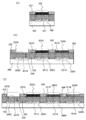
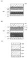


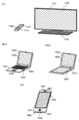
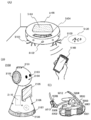

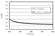


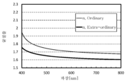
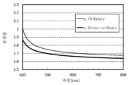


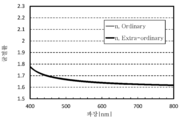


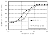


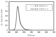

Classifications
-
- H01L51/5072—
-
- H—ELECTRICITY
- H10—SEMICONDUCTOR DEVICES; ELECTRIC SOLID-STATE DEVICES NOT OTHERWISE PROVIDED FOR
- H10K—ORGANIC ELECTRIC SOLID-STATE DEVICES
- H10K50/00—Organic light-emitting devices
- H10K50/10—OLEDs or polymer light-emitting diodes [PLED]
- H10K50/14—Carrier transporting layers
- H10K50/16—Electron transporting layers
-
- H—ELECTRICITY
- H10—SEMICONDUCTOR DEVICES; ELECTRIC SOLID-STATE DEVICES NOT OTHERWISE PROVIDED FOR
- H10K—ORGANIC ELECTRIC SOLID-STATE DEVICES
- H10K50/00—Organic light-emitting devices
- H10K50/10—OLEDs or polymer light-emitting diodes [PLED]
- H10K50/11—OLEDs or polymer light-emitting diodes [PLED] characterised by the electroluminescent [EL] layers
- H10K50/115—OLEDs or polymer light-emitting diodes [PLED] characterised by the electroluminescent [EL] layers comprising active inorganic nanostructures, e.g. luminescent quantum dots
-
- C—CHEMISTRY; METALLURGY
- C09—DYES; PAINTS; POLISHES; NATURAL RESINS; ADHESIVES; COMPOSITIONS NOT OTHERWISE PROVIDED FOR; APPLICATIONS OF MATERIALS NOT OTHERWISE PROVIDED FOR
- C09K—MATERIALS FOR MISCELLANEOUS APPLICATIONS, NOT PROVIDED FOR ELSEWHERE
- C09K11/00—Luminescent, e.g. electroluminescent, chemiluminescent materials
- C09K11/06—Luminescent, e.g. electroluminescent, chemiluminescent materials containing organic luminescent materials
-
- C—CHEMISTRY; METALLURGY
- C09—DYES; PAINTS; POLISHES; NATURAL RESINS; ADHESIVES; COMPOSITIONS NOT OTHERWISE PROVIDED FOR; APPLICATIONS OF MATERIALS NOT OTHERWISE PROVIDED FOR
- C09K—MATERIALS FOR MISCELLANEOUS APPLICATIONS, NOT PROVIDED FOR ELSEWHERE
- C09K11/00—Luminescent, e.g. electroluminescent, chemiluminescent materials
- C09K11/08—Luminescent, e.g. electroluminescent, chemiluminescent materials containing inorganic luminescent materials
- C09K11/77—Luminescent, e.g. electroluminescent, chemiluminescent materials containing inorganic luminescent materials containing rare earth metals
-
- H01L27/322—
-
- H01L51/0059—
-
- H01L51/0067—
-
- H01L51/5088—
-
- H—ELECTRICITY
- H05—ELECTRIC TECHNIQUES NOT OTHERWISE PROVIDED FOR
- H05B—ELECTRIC HEATING; ELECTRIC LIGHT SOURCES NOT OTHERWISE PROVIDED FOR; CIRCUIT ARRANGEMENTS FOR ELECTRIC LIGHT SOURCES, IN GENERAL
- H05B33/00—Electroluminescent light sources
- H05B33/12—Light sources with substantially two-dimensional radiating surfaces
- H05B33/14—Light sources with substantially two-dimensional radiating surfaces characterised by the chemical or physical composition or the arrangement of the electroluminescent material, or by the simultaneous addition of the electroluminescent material in or onto the light source
-
- H—ELECTRICITY
- H10—SEMICONDUCTOR DEVICES; ELECTRIC SOLID-STATE DEVICES NOT OTHERWISE PROVIDED FOR
- H10K—ORGANIC ELECTRIC SOLID-STATE DEVICES
- H10K50/00—Organic light-emitting devices
- H10K50/10—OLEDs or polymer light-emitting diodes [PLED]
- H10K50/17—Carrier injection layers
-
- H—ELECTRICITY
- H10—SEMICONDUCTOR DEVICES; ELECTRIC SOLID-STATE DEVICES NOT OTHERWISE PROVIDED FOR
- H10K—ORGANIC ELECTRIC SOLID-STATE DEVICES
- H10K50/00—Organic light-emitting devices
- H10K50/80—Constructional details
- H10K50/85—Arrangements for extracting light from the devices
- H10K50/852—Arrangements for extracting light from the devices comprising a resonant cavity structure, e.g. Bragg reflector pair
-
- H—ELECTRICITY
- H10—SEMICONDUCTOR DEVICES; ELECTRIC SOLID-STATE DEVICES NOT OTHERWISE PROVIDED FOR
- H10K—ORGANIC ELECTRIC SOLID-STATE DEVICES
- H10K50/00—Organic light-emitting devices
- H10K50/80—Constructional details
- H10K50/85—Arrangements for extracting light from the devices
- H10K50/854—Arrangements for extracting light from the devices comprising scattering means
-
- H—ELECTRICITY
- H10—SEMICONDUCTOR DEVICES; ELECTRIC SOLID-STATE DEVICES NOT OTHERWISE PROVIDED FOR
- H10K—ORGANIC ELECTRIC SOLID-STATE DEVICES
- H10K59/00—Integrated devices, or assemblies of multiple devices, comprising at least one organic light-emitting element covered by group H10K50/00
- H10K59/30—Devices specially adapted for multicolour light emission
- H10K59/38—Devices specially adapted for multicolour light emission comprising colour filters or colour changing media [CCM]
-
- H—ELECTRICITY
- H10—SEMICONDUCTOR DEVICES; ELECTRIC SOLID-STATE DEVICES NOT OTHERWISE PROVIDED FOR
- H10K—ORGANIC ELECTRIC SOLID-STATE DEVICES
- H10K85/00—Organic materials used in the body or electrodes of devices covered by this subclass
- H10K85/60—Organic compounds having low molecular weight
- H10K85/615—Polycyclic condensed aromatic hydrocarbons, e.g. anthracene
- H10K85/626—Polycyclic condensed aromatic hydrocarbons, e.g. anthracene containing more than one polycyclic condensed aromatic rings, e.g. bis-anthracene
-
- H—ELECTRICITY
- H10—SEMICONDUCTOR DEVICES; ELECTRIC SOLID-STATE DEVICES NOT OTHERWISE PROVIDED FOR
- H10K—ORGANIC ELECTRIC SOLID-STATE DEVICES
- H10K85/00—Organic materials used in the body or electrodes of devices covered by this subclass
- H10K85/60—Organic compounds having low molecular weight
- H10K85/631—Amine compounds having at least two aryl rest on at least one amine-nitrogen atom, e.g. triphenylamine
-
- H—ELECTRICITY
- H10—SEMICONDUCTOR DEVICES; ELECTRIC SOLID-STATE DEVICES NOT OTHERWISE PROVIDED FOR
- H10K—ORGANIC ELECTRIC SOLID-STATE DEVICES
- H10K85/00—Organic materials used in the body or electrodes of devices covered by this subclass
- H10K85/60—Organic compounds having low molecular weight
- H10K85/649—Aromatic compounds comprising a hetero atom
- H10K85/654—Aromatic compounds comprising a hetero atom comprising only nitrogen as heteroatom
-
- H01L2251/5369—
-
- H01L2251/55—
-
- H—ELECTRICITY
- H10—SEMICONDUCTOR DEVICES; ELECTRIC SOLID-STATE DEVICES NOT OTHERWISE PROVIDED FOR
- H10K—ORGANIC ELECTRIC SOLID-STATE DEVICES
- H10K2101/00—Properties of the organic materials covered by group H10K85/00
-
- H—ELECTRICITY
- H10—SEMICONDUCTOR DEVICES; ELECTRIC SOLID-STATE DEVICES NOT OTHERWISE PROVIDED FOR
- H10K—ORGANIC ELECTRIC SOLID-STATE DEVICES
- H10K2102/00—Constructional details relating to the organic devices covered by this subclass
- H10K2102/301—Details of OLEDs
- H10K2102/331—Nanoparticles used in non-emissive layers, e.g. in packaging layer
-
- H—ELECTRICITY
- H10—SEMICONDUCTOR DEVICES; ELECTRIC SOLID-STATE DEVICES NOT OTHERWISE PROVIDED FOR
- H10K—ORGANIC ELECTRIC SOLID-STATE DEVICES
- H10K50/00—Organic light-emitting devices
- H10K50/10—OLEDs or polymer light-emitting diodes [PLED]
- H10K50/19—Tandem OLEDs
-
- H—ELECTRICITY
- H10—SEMICONDUCTOR DEVICES; ELECTRIC SOLID-STATE DEVICES NOT OTHERWISE PROVIDED FOR
- H10K—ORGANIC ELECTRIC SOLID-STATE DEVICES
- H10K50/00—Organic light-emitting devices
- H10K50/80—Constructional details
- H10K50/86—Arrangements for improving contrast, e.g. preventing reflection of ambient light
-
- H—ELECTRICITY
- H10—SEMICONDUCTOR DEVICES; ELECTRIC SOLID-STATE DEVICES NOT OTHERWISE PROVIDED FOR
- H10K—ORGANIC ELECTRIC SOLID-STATE DEVICES
- H10K59/00—Integrated devices, or assemblies of multiple devices, comprising at least one organic light-emitting element covered by group H10K50/00
- H10K59/30—Devices specially adapted for multicolour light emission
- H10K59/35—Devices specially adapted for multicolour light emission comprising red-green-blue [RGB] subpixels
- H10K59/351—Devices specially adapted for multicolour light emission comprising red-green-blue [RGB] subpixels comprising more than three subpixels, e.g. red-green-blue-white [RGBW]
-
- H—ELECTRICITY
- H10—SEMICONDUCTOR DEVICES; ELECTRIC SOLID-STATE DEVICES NOT OTHERWISE PROVIDED FOR
- H10K—ORGANIC ELECTRIC SOLID-STATE DEVICES
- H10K85/00—Organic materials used in the body or electrodes of devices covered by this subclass
- H10K85/60—Organic compounds having low molecular weight
- H10K85/615—Polycyclic condensed aromatic hydrocarbons, e.g. anthracene
-
- H—ELECTRICITY
- H10—SEMICONDUCTOR DEVICES; ELECTRIC SOLID-STATE DEVICES NOT OTHERWISE PROVIDED FOR
- H10K—ORGANIC ELECTRIC SOLID-STATE DEVICES
- H10K85/00—Organic materials used in the body or electrodes of devices covered by this subclass
- H10K85/60—Organic compounds having low molecular weight
- H10K85/631—Amine compounds having at least two aryl rest on at least one amine-nitrogen atom, e.g. triphenylamine
- H10K85/636—Amine compounds having at least two aryl rest on at least one amine-nitrogen atom, e.g. triphenylamine comprising heteroaromatic hydrocarbons as substituents on the nitrogen atom
-
- H—ELECTRICITY
- H10—SEMICONDUCTOR DEVICES; ELECTRIC SOLID-STATE DEVICES NOT OTHERWISE PROVIDED FOR
- H10K—ORGANIC ELECTRIC SOLID-STATE DEVICES
- H10K85/00—Organic materials used in the body or electrodes of devices covered by this subclass
- H10K85/60—Organic compounds having low molecular weight
- H10K85/649—Aromatic compounds comprising a hetero atom
- H10K85/657—Polycyclic condensed heteroaromatic hydrocarbons
- H10K85/6572—Polycyclic condensed heteroaromatic hydrocarbons comprising only nitrogen in the heteroaromatic polycondensed ring system, e.g. phenanthroline or carbazole
-
- H—ELECTRICITY
- H10—SEMICONDUCTOR DEVICES; ELECTRIC SOLID-STATE DEVICES NOT OTHERWISE PROVIDED FOR
- H10K—ORGANIC ELECTRIC SOLID-STATE DEVICES
- H10K85/00—Organic materials used in the body or electrodes of devices covered by this subclass
- H10K85/60—Organic compounds having low molecular weight
- H10K85/649—Aromatic compounds comprising a hetero atom
- H10K85/657—Polycyclic condensed heteroaromatic hydrocarbons
- H10K85/6574—Polycyclic condensed heteroaromatic hydrocarbons comprising only oxygen in the heteroaromatic polycondensed ring system, e.g. cumarine dyes
-
- H—ELECTRICITY
- H10—SEMICONDUCTOR DEVICES; ELECTRIC SOLID-STATE DEVICES NOT OTHERWISE PROVIDED FOR
- H10K—ORGANIC ELECTRIC SOLID-STATE DEVICES
- H10K85/00—Organic materials used in the body or electrodes of devices covered by this subclass
- H10K85/60—Organic compounds having low molecular weight
- H10K85/649—Aromatic compounds comprising a hetero atom
- H10K85/657—Polycyclic condensed heteroaromatic hydrocarbons
- H10K85/6576—Polycyclic condensed heteroaromatic hydrocarbons comprising only sulfur in the heteroaromatic polycondensed ring system, e.g. benzothiophene
Abstract
Description
본 발명의 일 형태는 유기 화합물, 발광 소자, 발광 디바이스, 디스플레이 모듈, 조명 모듈, 표시 장치, 발광 장치, 전자 기기, 조명 장치, 및 전자 디바이스에 관한 것이다. 또한 본 발명의 일 형태는 상기 기술분야에 한정되지 않는다. 본 명세서 등에서 개시(開示)하는 발명의 일 형태가 속하는 기술분야는 물건, 방법, 또는 제조 방법에 관한 것이다. 또는 본 발명의 일 형태는 공정(process), 기계(machine), 제품(manufacture), 또는 조성물(composition of matter)에 관한 것이다. 따라서 본 명세서에서 개시하는 본 발명의 일 형태가 속하는 기술분야의 더 구체적인 예로서는 반도체 장치, 표시 장치, 액정 표시 장치, 발광 장치, 조명 장치, 축전 장치, 기억 장치, 촬상 장치, 이들의 구동 방법, 또는 이들의 제조 방법을 들 수 있다.One embodiment of the present invention relates to an organic compound, a light emitting element, a light emitting device, a display module, a lighting module, a display device, a light emitting device, an electronic device, a lighting device, and an electronic device. In addition, one embodiment of the present invention is not limited to the above technical field. The technical field to which one embodiment of the invention disclosed in this specification and the like belongs relates to an object, a method, or a manufacturing method. Or one aspect of the present invention relates to a process, a machine, a manufacture, or a composition of matter. Therefore, as a more specific example of the technical field to which one embodiment of the present invention disclosed in the present specification belongs, a semiconductor device, a display device, a liquid crystal display device, a light-emitting device, a lighting device, a power storage device, a memory device, an imaging device, a driving method thereof, or These manufacturing methods are mentioned.
유기 화합물을 사용하고 일렉트로루미네선스(EL: Electroluminescence)를 이용하는 발광 디바이스(유기 EL 디바이스)의 실용화가 진행되고 있다. 이들 발광 디바이스의 기본적인 구성은 발광 재료를 포함하는 유기 화합물층(EL층)을 한 쌍의 전극 사이에 끼운 것이다. 이 디바이스에 전압을 인가하여 캐리어를 주입하고, 상기 캐리어의 재결합 에너지를 이용함으로써, 발광 재료로부터의 발광을 얻을 수 있다.Practical use of a light-emitting device (organic EL device) using an organic compound and electroluminescence (EL) is in progress. The basic configuration of these light-emitting devices is that an organic compound layer (EL layer) containing a light-emitting material is sandwiched between a pair of electrodes. By applying a voltage to this device, injecting carriers, and using the recombination energy of the carriers, light emission from the luminescent material can be obtained.
이와 같은 발광 디바이스는 자발광형이기 때문에, 디스플레이의 화소로서 사용하면 액정에 비하여 시인성이 높고 백라이트가 불필요하다는 등의 장점이 있어, 플랫 패널 디스플레이용 소자로서 적합하다. 또한 이와 같은 발광 디바이스를 사용한 디스플레이는 얇고 가볍게 제작할 수 있다는 것도 큰 장점이다. 또한 응답 속도가 매우 빠르다는 것도 특징 중 하나이다.Since such a light-emitting device is of a self-luminous type, when used as a pixel of a display, it has advantages such as high visibility and no need for a backlight, and is suitable as an element for a flat panel display. In addition, it is also a great advantage that a display using such a light emitting device can be manufactured thin and light. Also, one of the features is that the response speed is very fast.
또한 이들 발광 디바이스는 발광층을 이차원으로 연속하여 형성할 수 있기 때문에 면발광을 얻을 수 있다. 이것은 백열 전구나 LED로 대표되는 점광원, 또는 형광등으로 대표되는 선광원으로는 얻기 어려운 특색이기 때문에, 조명 등에 응용할 수 있는 면광원으로서의 이용 가치도 높다.In addition, since these light-emitting devices can form light-emitting layers continuously in two dimensions, surface light emission can be obtained. Since this is a characteristic that is difficult to obtain with a point light source represented by an incandescent light bulb or an LED, or a line light source represented by a fluorescent lamp, the use value as a surface light source that can be applied to lighting or the like is also high.
이와 같이 발광 디바이스를 사용한 디스플레이나 조명 장치는 다양한 전자 기기에 적합하게 적용되지만, 특성이 더 양호한 발광 디바이스를 위하여 연구 개발이 진행되고 있다.As described above, a display or a lighting device using a light emitting device is suitably applied to various electronic devices, but research and development are being conducted for a light emitting device having better characteristics.
광 추출 효율이 낮다는 것이 유기 EL 디바이스의 문제 중 하나로서 자주 제기된다. 특히, 인접한 층들의 굴절률의 차이에 기인하는 반사로 인한 감쇠는, 디바이스의 효율을 저하시키는 큰 요인이 된다. 이 영향을 줄이기 위하여, 굴절률이 낮은 재료로 이루어지는 층을 EL층 내부에 형성하는 구성이 제안되고 있다(예를 들어 특허문헌 1, 비특허문헌 1 참조).The low light extraction efficiency is often raised as one of the problems of organic EL devices. In particular, attenuation due to reflection due to a difference in refractive index of adjacent layers becomes a large factor in deteriorating the efficiency of the device. In order to reduce this influence, a configuration in which a layer made of a material having a low refractive index is formed inside the EL layer has been proposed (see, for example,
이 구성을 가지는 발광 디바이스는, 종래의 구성을 가지는 발광 디바이스보다 광 추출 효율, 나아가서는 외부 양자 효율을 높게 할 수 있지만, 발광 디바이스에서의 그 외의 중요한 특성에 악영향을 미치지 않고 EL층 내부에 상기와 같은 굴절률이 낮은 층을 형성하는 것은 용이한 것이 아니다. 이것은, 낮은 굴절률과 높은 캐리어 수송성 또는 발광 디바이스에 사용한 경우의 신뢰성이 트레이드오프의 관계에 있기 때문이다. 이 문제는, 유기 화합물의 캐리어 수송성이나 신뢰성은 불포화 결합의 존재에 크게 의존하고, 불포화 결합을 많이 가지는 유기 화합물은 굴절률이 높은 경향이 있는 것에 원인이 있다.A light-emitting device having this configuration can increase light extraction efficiency and further external quantum efficiency than a light-emitting device having a conventional configuration, but the above and the inside of the EL layer do not adversely affect other important characteristics in the light-emitting device. It is not easy to form a layer having the same refractive index. This is because there is a trade-off relationship between a low refractive index and a high carrier transport property or reliability when used in a light emitting device. This problem is due to the fact that the carrier transportability and reliability of the organic compound largely depend on the presence of unsaturated bonds, and the organic compound having many unsaturated bonds tends to have a high refractive index.
한편, 색 변환 방식을 사용한 디스플레이의 실용화가 진행되고 있다. 색 변환 방식이란, 포토루미네선스를 나타내는 물질에 발광 디바이스로부터의 광을 조사함으로써, 광을 원하는 색의 광으로 변환하는 방식을 말한다. 색 변환 방식의 디스플레이에는, 포토루미네선스의 효율에 따르기도 하지만, 발광 디바이스로부터의 광을 단순히 저감하는 컬러 필터 방식의 디스플레이와 비교하여, 에너지 손실이 적고 소비전력이 낮은 디스플레이를 얻기 쉽다는 특징이 있다.On the other hand, practical use of displays using a color conversion method is in progress. The color conversion method refers to a method of converting light into light of a desired color by irradiating light from a light emitting device to a material exhibiting photoluminescence. The color conversion type display depends on the efficiency of photoluminescence, but compared to a color filter type display that simply reduces the light from a light emitting device, it is characterized in that it is easy to obtain a display with low energy loss and low power consumption. There is this.
그러므로, 본 발명의 일 형태에서는 신규 발광 장치를 제공하는 것을 과제로 한다. 또는 발광 효율이 높은 발광 장치를 제공하는 것을 과제로 한다. 또는 수명이 긴 발광 장치를 제공하는 것을 과제로 한다. 또는 구동 전압이 낮은 발광 장치를 제공하는 것을 과제로 한다.Therefore, in one embodiment of the present invention, it is an object to provide a novel light emitting device. Alternatively, it is an object to provide a light-emitting device having high luminous efficiency. Alternatively, it is an object to provide a light emitting device having a long life. Alternatively, it is an object to provide a light emitting device having a low driving voltage.
또는 본 발명의 다른 일 형태에서는 신뢰성이 높은 전자 기기 또는 표시 장치를 각각 제공하는 것을 과제로 한다. 또는 본 발명의 다른 일 형태에서는 소비전력이 낮은 전자 기기 또는 표시 장치를 각각 제공하는 것을 과제로 한다.Another object of the present invention is to provide an electronic device or display device with high reliability, respectively. Another object of the present invention is to provide an electronic device or a display device with low power consumption, respectively.
본 발명은 상술한 과제 중 어느 하나의 과제를 해결하면 좋은 것으로 한다.The present invention is supposed to solve any one of the above-described problems.
본 발명의 일 형태는, 제 1 발광 디바이스와 제 1 색 변환층을 가지는 발광 장치이고, 상기 제 1 발광 디바이스는 양극과, 음극과, 상기 양극과 상기 음극 사이에 위치하는 EL층을 가지고, 상기 EL층은 467nm의 파장의 광에 대한 굴절률이 1.75 이하인 재료를 포함하는 층을 가지고, 상기 제 1 색 변환층은 광을 흡수하고 발광하는 제 1 물질을 포함하고, 상기 제 1 발광 디바이스로부터 방출되는 광이 상기 제 1 색 변환층에 조사되는 발광 장치이다.One aspect of the present invention is a light emitting device having a first light emitting device and a first color conversion layer, the first light emitting device has an anode, a cathode, and an EL layer positioned between the anode and the cathode, the The EL layer has a layer comprising a material having a refractive index of 1.75 or less for light with a wavelength of 467 nm, the first color conversion layer comprising a first material that absorbs and emit light, and is emitted from the first light emitting device. It is a light-emitting device in which light is irradiated to the first color conversion layer.
또한 본 발명의 다른 일 형태는, 제 1 발광 디바이스와 제 1 색 변환층을 가지는 발광 장치이고, 상기 제 1 발광 디바이스는 양극과, 음극과, 상기 양극과 상기 음극 사이에 위치하는 EL층을 가지고, 상기 EL층은 467nm의 파장의 광에 대한 굴절률이 1.75 이하인 층을 가지고, 상기 제 1 색 변환층은 광을 흡수하고 발광하는 제 1 물질을 포함하고, 상기 제 1 발광 디바이스로부터 방출되는 광이 상기 제 1 색 변환층에 조사되는 발광 장치이다.Another aspect of the present invention is a light emitting device having a first light emitting device and a first color conversion layer, wherein the first light emitting device has an anode, a cathode, and an EL layer positioned between the anode and the cathode. , The EL layer has a layer having a refractive index of 1.75 or less for light having a wavelength of 467 nm, the first color conversion layer includes a first material that absorbs and emit light, and the light emitted from the first light emitting device is It is a light-emitting device irradiated to the first color conversion layer.
또는 본 발명의 다른 일 형태는, 제 1 발광 디바이스와 제 1 색 변환층을 가지는 발광 장치이고, 상기 제 1 발광 디바이스는 양극과, 음극과, 상기 양극과 상기 음극 사이에 위치하는 EL층을 가지고, 상기 EL층은 발광층과 정공 주입층을 가지고, 상기 정공 주입층은 상기 양극에 접하여 제공되고, 상기 정공 주입층은 467nm의 파장의 광에 대한 굴절률이 1.75 이하인 유기 화합물을 포함하고, 상기 제 1 색 변환층은 광을 흡수하고 발광하는 제 1 물질을 포함하고, 상기 제 1 발광 디바이스로부터 방출되는 광이 상기 제 1 색 변환층에 조사되는 발광 장치이다.Or another aspect of the present invention is a light emitting device having a first light emitting device and a first color conversion layer, wherein the first light emitting device has an anode, a cathode, and an EL layer positioned between the anode and the cathode. , The EL layer has an emission layer and a hole injection layer, the hole injection layer is provided in contact with the anode, the hole injection layer includes an organic compound having a refractive index of 1.75 or less for light having a wavelength of 467 nm, and the first The color conversion layer is a light-emitting device including a first material that absorbs light and emits light, and the light emitted from the first light-emitting device is irradiated onto the first color conversion layer.
또는 본 발명의 다른 일 형태는, 상기 구성에서 상기 467nm의 파장의 광에 대한 굴절률이 1.75 이하인 유기 화합물이 제 1 방향족 고리, 제 2 방향족 고리, 및 제 3 방향족 고리를 가지는 모노아민 화합물이고, 상기 제 1 방향족 고리, 상기 제 2 방향족 고리, 및 상기 제 3 방향족 고리는 상기 모노아민 화합물의 질소 원자에 결합되고, 분자 내의 총탄소수에 대한 sp3 혼성 궤도로 결합을 형성하는 탄소의 비율이 23% 이상 55% 이하의 유기 화합물인 발광 장치이다.Alternatively, in another aspect of the present invention, the organic compound having a refractive index of 1.75 or less for light having a wavelength of 467 nm in the above configuration is a monoamine compound having a first aromatic ring, a second aromatic ring, and a third aromatic ring, and the The first aromatic ring, the second aromatic ring, and the third aromatic ring are bonded to the nitrogen atom of the monoamine compound, and the proportion of carbon forming a bond by sp3 hybrid orbital to the total number of carbon atoms in the molecule is 23% or more. It is a light-emitting device of 55% or less of an organic compound.
또는 본 발명의 다른 일 형태는, 상기 구성에서 상기 467nm의 파장의 광에 대한 굴절률이 1.75 이하인 유기 화합물이 하기 일반식(G1)으로 나타내어지는 유기 화합물인 발광 장치이다.Alternatively, another aspect of the present invention is a light emitting device in which the organic compound having a refractive index of 1.75 or less for light having a wavelength of 467 nm in the above configuration is an organic compound represented by the following general formula (G1).
[화학식 1][Formula 1]

다만 상기 일반식(G1)에서, Ar1, Ar2는 각각 독립적으로 벤젠 고리를 가지는 치환기 혹은 2개 또는 3개의 벤젠 고리가 서로 결합된 치환기를 나타낸다. 다만 Ar1 및 Ar2 중 한쪽 또는 양쪽은 sp3 혼성 궤도만으로 결합을 형성하는 탄소수 1 내지 12의 탄화수소기를 하나 또는 복수로 가지고, Ar1 및 Ar2에 결합된 상기 탄화수소기에 포함되는 탄소의 총수는 8 이상이고, 또한 Ar1 및 Ar2 중 적어도 한쪽에 결합된 상기 탄화수소기에 포함되는 탄소의 총수는 6 이상이다. 또한 상기 탄화수소기로서 Ar1 또는 Ar2에 탄소수 1 또는 2의 직쇄 알킬기가 복수로 결합되는 경우, 상기 직쇄 알킬기들이 결합되어 고리를 형성하여도 좋다. 또한 상기 일반식(G1)에서, R1 및 R2는 각각 독립적으로 탄소수 1 내지 4의 알킬기를 나타낸다. 또한 R1 및 R2는 서로 결합되어 고리를 형성하여도 좋다. 또한 R3은 탄소수 1 내지 4의 알킬기를 나타내고, u는 0 내지 4의 정수(整數)이다.However, in the general formula (G1), Ar 1 and Ar 2 each independently represent a substituent having a benzene ring or a substituent in which two or three benzene rings are bonded to each other. However , one or both of Ar 1 and Ar 2 has one or more hydrocarbon groups having 1 to 12 carbon atoms forming bonds only with sp3 hybrid orbitals, and the total number of carbons included in the hydrocarbon group bonded to Ar 1 and Ar 2 is 8 And the total number of carbons contained in the hydrocarbon group bonded to at least one of Ar 1 and Ar 2 is 6 or more. In addition, when a plurality of linear alkyl groups having 1 or 2 carbon atoms are bonded to Ar 1 or Ar 2 as the hydrocarbon group, the linear alkyl groups may be bonded to form a ring. In addition, in the general formula (G1), R 1 and R 2 each independently represent an alkyl group having 1 to 4 carbon atoms. Further, R 1 and R 2 may be bonded to each other to form a ring. Further, R 3 represents an alkyl group having 1 to 4 carbon atoms, and u is an integer of 0 to 4.
또는 본 발명의 다른 일 형태는, 제 1 발광 디바이스와 제 1 색 변환층을 가지는 발광 장치이고, 상기 제 1 발광 디바이스는 양극과, 음극과, 상기 양극과 상기 음극 사이에 위치하는 EL층을 가지고, 상기 EL층은 발광층과 전자 수송층을 가지고, 상기 전자 수송층은 상기 발광층과 상기 음극 사이에 위치하고, 상기 전자 수송층은 467nm의 파장의 광에 대한 굴절률이 1.75 이하인 재료를 가지고, 상기 제 1 색 변환층은 광을 흡수하고 발광하는 제 1 물질을 포함하고, 상기 제 1 발광 디바이스로부터 방출되는 광이 상기 제 1 색 변환층에 조사되는 발광 장치이다.Or another aspect of the present invention is a light emitting device having a first light emitting device and a first color conversion layer, wherein the first light emitting device has an anode, a cathode, and an EL layer positioned between the anode and the cathode. , The EL layer has a light emitting layer and an electron transport layer, the electron transport layer is located between the light emitting layer and the cathode, the electron transport layer has a material having a refractive index of 1.75 or less for light having a wavelength of 467 nm, the first color conversion layer Silver is a light-emitting device comprising a first material that absorbs light and emits light, and the light emitted from the first light-emitting device is irradiated onto the first color conversion layer.
또는 본 발명의 다른 일 형태는, 상기 구성에서 상기 굴절률이 1.75 이하인 재료가, 전자 수송성을 가지는 유기 화합물과 무기 화합물의 혼합 재료이고, 상기 무기 화합물이 알칼리 금속의 플루오린화물 또는 알칼리 토금속의 플루오린화물인 발광 장치이다.Alternatively, in another aspect of the present invention, in the above configuration, the material having a refractive index of 1.75 or less is a mixed material of an organic compound and an inorganic compound having electron transport properties, and the inorganic compound is a fluoride of an alkali metal or fluorine of an alkaline earth metal. It is a light emitting device that is a cargo.
또는 본 발명의 다른 일 형태는, 상기 구성에서 상기 무기 화합물이 알칼리 금속이고, 상기 전자 수송층에서의 상기 무기 화합물의 농도가 50vol% 이상인 발광 장치이다.Alternatively, another aspect of the present invention is a light-emitting device in which the inorganic compound is an alkali metal in the above configuration, and the concentration of the inorganic compound in the electron transport layer is 50 vol% or more.
또는 본 발명의 다른 일 형태는, 상기 구성에서 상기 무기 화합물이 알칼리 금속이고, 상기 전자 수송층에서의 상기 무기 화합물의 농도가 50vol% 이상 95vol% 미만인 발광 장치이다.Alternatively, another aspect of the present invention is a light emitting device in which the inorganic compound is an alkali metal in the above configuration, and the concentration of the inorganic compound in the electron transport layer is 50 vol% or more and less than 95 vol%.
또는 본 발명의 다른 일 형태는, 상기 구성에서 상기 전자 수송층에서의 상기 무기 화합물의 농도가 20vol% 이상인 발광 장치이다.Alternatively, another aspect of the present invention is a light emitting device in which the concentration of the inorganic compound in the electron transport layer is 20 vol% or more in the above configuration.
또는 본 발명의 다른 일 형태는, 상기 구성에서 제 1 발광 디바이스와 제 1 색 변환층을 가지는 발광 장치이고, 상기 제 1 발광 디바이스는 양극과, 음극과, 상기 양극과 상기 음극 사이에 위치하는 EL층을 가지고, 상기 EL층은 정공 주입층과 발광층과 전자 수송층을 가지고, 상기 정공 주입층은 상기 양극과 상기 발광층 사이에 위치하고, 상기 전자 수송층은 상기 발광층과 상기 음극 사이에 위치하고, 상기 정공 주입층은 467nm의 파장의 광에 대한 굴절률이 1.75 이하인 유기 화합물을 가지고, 상기 전자 수송층은 467nm의 파장의 광에 대한 굴절률이 1.75 이하인 재료를 가지고, 상기 제 1 색 변환층은 광을 흡수하고 발광하는 제 1 물질을 가지고, 상기 제 1 발광 디바이스로부터 방출되는 광이 상기 제 1 색 변환층에 조사되는 발광 장치이다.Alternatively, another aspect of the present invention is a light emitting device having a first light emitting device and a first color conversion layer in the above configuration, wherein the first light emitting device is an anode, a cathode, and an EL positioned between the anode and the cathode. Has a layer, the EL layer has a hole injection layer, a light emitting layer, and an electron transport layer, the hole injection layer is located between the anode and the light emitting layer, the electron transport layer is located between the light emitting layer and the cathode, the hole injection layer Silver has an organic compound having a refractive index of 1.75 or less for light having a wavelength of 467 nm, the electron transport layer has a material having a refractive index of 1.75 or less for light having a wavelength of 467 nm, and the first color conversion layer absorbs light and emits light. It is a light-emitting device having one material and in which light emitted from the first light-emitting device is irradiated onto the first color conversion layer.
또는 본 발명의 다른 일 형태는, 상기 구성에서 상기 제 1 발광 디바이스로부터 얻어지는 발광 스펙트럼의 피크 파장이 440nm 내지 520nm에 존재하는 발광 장치이다.Alternatively, another aspect of the present invention is a light-emitting device in which the peak wavelength of the emission spectrum obtained from the first light-emitting device in the above configuration is between 440 nm and 520 nm.
또는 본 발명의 다른 일 형태는, 제 1 발광 디바이스와 제 1 색 변환층을 가지는 발광 장치이고, 상기 제 1 발광 디바이스는 양극과, 음극과, 상기 양극과 상기 음극 사이에 위치하는 EL층을 가지고, 상기 EL층은 정공 주입층과 발광층과 전자 수송층을 가지고, 상기 정공 주입층은 상기 양극과 상기 발광층 사이에 위치하고, 상기 전자 수송층은 상기 발광층과 상기 음극 사이에 위치하고, 상기 정공 주입층은 467nm의 파장의 광에 대한 굴절률이 1.75 이하인 유기 화합물을 가지고, 상기 전자 수송층은 467nm의 파장의 광에 대한 굴절률이 1.75 이하인 재료를 가지고, 상기 제 1 색 변환층은 광을 흡수하고 발광하는 제 1 물질을 가지고, 상기 제 1 발광 디바이스로부터 방출되는 광이 상기 제 1 색 변환층에 조사되는 발광 장치이다.Or another aspect of the present invention is a light emitting device having a first light emitting device and a first color conversion layer, wherein the first light emitting device has an anode, a cathode, and an EL layer positioned between the anode and the cathode. , The EL layer has a hole injection layer, an emission layer, and an electron transport layer, the hole injection layer is located between the anode and the emission layer, the electron transport layer is located between the emission layer and the cathode, and the hole injection layer is 467 nm. An organic compound having a refractive index of 1.75 or less for light of a wavelength, the electron transport layer has a material having a refractive index of 1.75 or less for light of a wavelength of 467 nm, and the first color conversion layer comprises a first material that absorbs light and emits light. It is a light-emitting device in which light emitted from the first light-emitting device is irradiated onto the first color conversion layer.
또는 본 발명의 다른 일 형태는, 상기 구성에서 상기 제 1 물질이 퀀텀닷(quantum dot)인 발광 장치이다.Alternatively, another aspect of the present invention is a light emitting device in which the first material is a quantum dot in the above configuration.
또는 본 발명의 다른 일 형태는, 상기 구성에서 상기 제 1 발광 디바이스가 미소 공진 구조를 가지는 발광 장치이다.Alternatively, another aspect of the present invention is a light emitting device in which the first light emitting device has a microscopic resonance structure in the above configuration.
또는 본 발명의 다른 일 형태는, 상기 구성에서 상기 발광 장치가 제 2 발광 디바이스와 제 3 발광 디바이스와 제 2 색 변환층을 더 가지고, 상기 제 2 발광 디바이스 및 상기 제 3 발광 디바이스가 상기 제 1 발광 디바이스와 같은 구조를 가지고, 상기 제 2 색 변환층이 광을 흡수하고 발광하는 제 2 물질을 가지고, 상기 제 1 물질의 발광 스펙트럼의 피크 파장과 상기 제 2 물질의 발광 스펙트럼의 피크 파장이 상이하고, 상기 제 2 발광 디바이스로부터 방출되는 광이 상기 제 2 색 변환층에 조사되는 발광 장치이다.Alternatively, in another aspect of the present invention, in the above configuration, the light-emitting device further has a second light-emitting device, a third light-emitting device, and a second color conversion layer, and the second light-emitting device and the third light-emitting device are the first It has the same structure as a light emitting device, the second color conversion layer has a second material that absorbs light and emits light, and the peak wavelength of the emission spectrum of the first material and the peak wavelength of the emission spectrum of the second material are different. And the light emitted from the second light emitting device is irradiated onto the second color conversion layer.
또는 본 발명의 다른 일 형태는, 상기 구성에서 상기 제 2 물질이 퀀텀닷인 발광 장치이다.Alternatively, another aspect of the present invention is a light emitting device in which the second material is a quantum dot in the above configuration.
또는 본 발명의 다른 일 형태는, 상기 구성에서 상기 제 1 물질의 발광 스펙트럼의 피크 파장이 500nm 내지 600nm에 존재하고, 상기 제 2 물질의 발광 스펙트럼의 피크 파장이 600nm 내지 750nm에 존재하는 발광 장치이다.Alternatively, another aspect of the present invention is a light emitting device in which the peak wavelength of the emission spectrum of the first material in the above configuration is 500 nm to 600 nm, and the peak wavelength of the emission spectrum of the second material is 600 nm to 750 nm. .
또는 본 발명의 다른 일 형태는, 상기 구성에서 상기 발광 장치가 제 4 발광 디바이스와 제 3 색 변환층을 더 가지고, 상기 제 4 발광 디바이스가 상기 제 1 발광 디바이스와 같은 구조를 가지고, 상기 제 3 색 변환층이 광을 흡수하고 발광하는 제 3 물질을 가지고, 상기 제 3 물질의 발광 스펙트럼의 피크 파장이 560nm 내지 610nm에 존재하고, 상기 제 4 발광 디바이스로부터 방출되는 광이 상기 제 3 색 변환층에 조사되는 발광 장치이다.Alternatively, in another aspect of the present invention, in the above configuration, the light emitting device further has a fourth light emitting device and a third color conversion layer, the fourth light emitting device has the same structure as the first light emitting device, and the third The color conversion layer has a third material that absorbs light and emits light, the peak wavelength of the emission spectrum of the third material is in 560 nm to 610 nm, and the light emitted from the fourth light emitting device is the third color conversion layer It is a light emitting device that is irradiated to.
또는 본 발명의 다른 일 형태는, 상기 구성에서 상기 제 3 물질이 희토류 원소를 포함하는 발광 장치이다.Alternatively, another aspect of the present invention is a light emitting device in which the third material contains a rare earth element in the above configuration.
또는 본 발명의 다른 일 형태는, 상기 구성에서 상기 희토류 원소가 유로퓸, 세륨, 및 이트륨 중 적어도 하나인 발광 장치이다.Alternatively, another aspect of the present invention is a light emitting device in which the rare earth element is at least one of europium, cerium, and yttrium in the above configuration.
또는 본 발명의 다른 일 형태는, 상기 구성에서 상기 제 3 물질이 퀀텀닷인 발광 장치이다.Alternatively, another aspect of the present invention is a light emitting device in which the third material is a quantum dot in the above configuration.
또는 본 발명의 다른 일 형태는, 상기 구성에서 상기 제 3 색 변환층으로부터 얻어지는 발광 스펙트럼에 2개의 피크가 존재하는 발광 장치이다.Alternatively, another aspect of the present invention is a light emitting device in which two peaks exist in the emission spectrum obtained from the third color conversion layer in the above configuration.
또는 본 발명의 다른 일 형태는, 상기 구성에서 상기 제 3 색 변환층으로부터 얻어지는 발광이 백색 발광인 발광 장치이다.Alternatively, another aspect of the present invention is a light-emitting device in which light emission obtained from the third color conversion layer in the above configuration is white light emission.
또는 본 발명의 다른 일 형태는, 상기 구성에서 상기 발광 디바이스가 복수의 발광층을 가지는 발광 장치이다.Alternatively, another aspect of the present invention is a light-emitting device in which the light-emitting device has a plurality of light-emitting layers in the above configuration.
또는 본 발명의 다른 일 형태는, 상기 구성에서 상기 복수의 발광층들 사이에 전하 발생층을 가지는 발광 장치이다.Alternatively, another aspect of the present invention is a light emitting device having a charge generation layer between the plurality of light emitting layers in the above configuration.
또는 본 발명의 다른 일 형태는, 상기 구성에서 상기 제 1 발광 디바이스가 청색 발광을 나타내는 발광 장치이다.Alternatively, another aspect of the present invention is a light emitting device in which the first light emitting device emits blue light in the above configuration.
또는 본 발명의 다른 일 형태는, 상기 구성에서 상기 발광 장치가 컬러 필터를 가지고, 상기 제 1 색 변환층이 상기 제 1 발광 디바이스와 상기 컬러 필터 사이에 위치하는 발광 장치이다.Alternatively, another aspect of the present invention is a light-emitting device in the above configuration, wherein the light-emitting device has a color filter, and the first color conversion layer is positioned between the first light-emitting device and the color filter.
또는 본 발명의 다른 일 형태는 상술한 것 중 어느 것에 기재된 발광 디바이스와, 센서, 조작 버튼, 스피커, 또는 마이크로폰을 가지는 전자 기기이다.Alternatively, another embodiment of the present invention is an electronic device having the light emitting device described in any one of the above, and a sensor, an operation button, a speaker, or a microphone.
또는 본 발명의 다른 일 형태는 상술한 것 중 어느 것에 기재된 발광 디바이스와, 트랜지스터 또는 기판을 가지는 발광 장치이다.Alternatively, another embodiment of the present invention is a light emitting device including the light emitting device described in any of the above and a transistor or a substrate.
또는 본 발명의 다른 일 형태는 상술한 것 중 어느 것에 기재된 발광 디바이스와, 하우징을 가지는 조명 장치이다.Alternatively, another embodiment of the present invention is a lighting device having a light emitting device according to any one of the above and a housing.
또한 본 명세서에서 발광 장치는, 발광 디바이스를 사용한 화상 표시 디바이스를 포함한다. 또한 발광 디바이스에 커넥터, 예를 들어 이방 도전성 필름 또는 TCP(Tape Carrier Package)가 장착된 모듈, TCP 끝에 인쇄 배선 기판이 제공된 모듈, 또는 COG(Chip On Glass) 방식에 의하여 발광 디바이스에 IC(집적 회로)가 직접 실장된 모듈도 발광 장치에 포함되는 경우가 있다. 또한 조명 기구 등은 발광 장치를 가지는 경우가 있다.In addition, in this specification, the light-emitting device includes an image display device using a light-emitting device. In addition, the light emitting device is equipped with a connector, for example, an anisotropic conductive film or a TCP (Tape Carrier Package) module, a module provided with a printed wiring board at the end of the TCP, or an IC (Integrated Circuit) in the light emitting device by the COG (Chip On Glass) method. Modules on which) is directly mounted are also included in the light emitting device in some cases. In addition, the lighting equipment and the like may have a light-emitting device.
본 발명의 일 형태에서는 신규 발광 장치를 제공할 수 있다. 또는 발광 효율이 높은 발광 장치를 제공할 수 있다. 또는 수명이 긴 발광 장치를 제공할 수 있다. 또는 구동 전압이 낮은 발광 장치를 제공할 수 있다.In one embodiment of the present invention, a novel light emitting device can be provided. Alternatively, a light-emitting device having high luminous efficiency can be provided. Alternatively, a light emitting device having a long life can be provided. Alternatively, a light emitting device having a low driving voltage may be provided.
또는 본 발명의 다른 일 형태에서는 신뢰성이 높은 전자 기기 또는 표시 장치를 각각 제공할 수 있다. 또는 본 발명의 다른 일 형태에서는 소비전력이 낮은 전자 기기 또는 표시 장치를 각각 제공할 수 있다.Alternatively, in another embodiment of the present invention, an electronic device or a display device having high reliability can be provided, respectively. Alternatively, in another embodiment of the present invention, an electronic device or a display device having low power consumption may be provided.
또한 이들 효과의 기재는 다른 효과의 존재를 방해하는 것은 아니다. 또한 본 발명의 일 형태는 이들 효과 모두를 반드시 가질 필요는 없다. 또한 이들 외의 효과는 명세서, 도면, 청구항 등의 기재로부터 저절로 명백해지는 것이며, 명세서, 도면, 청구항 등의 기재로부터 이들 외의 효과를 추출할 수 있다.In addition, the description of these effects does not interfere with the existence of other effects. In addition, one embodiment of the present invention does not necessarily have to have all of these effects. In addition, effects other than these will become apparent from the description of the specification, drawings, claims, and the like, and other effects can be extracted from the description of the specification, drawings, claims, and the like.
도 1의 (A), (B), 및 (C)는 발광 장치의 개념도이다.
도 2의 (A), (B), 및 (C)는 발광 디바이스의 개략도이다.
도 3은 발광 디바이스의 개략도이다.
도 4의 (A), (B), 및 (C)는 발광 장치의 개념도이다.
도 5의 (A), (B), 및 (C)는 발광 장치의 개념도이다.
도 6의 (A) 및 (B)는 패시브 매트릭스형 발광 장치의 개념도이다.
도 7의 (A) 및 (B)는 액티브 매트릭스형 발광 장치의 개념도이다.
도 8의 (A) 및 (B)는 액티브 매트릭스형 발광 장치의 개념도이다.
도 9는 액티브 매트릭스형 발광 장치의 개념도이다.
도 10의 (A), (B1), (B2), 및 (C)는 전자 기기를 나타낸 도면이다.
도 11의 (A), (B), 및 (C)는 전자 기기를 나타낸 도면이다.
도 12는 차량 탑재 표시 장치 및 조명 장치를 나타낸 도면이다.
도 13의 (A) 및 (B)는 전자 기기를 나타낸 도면이다.
도 14의 (A), (B), 및 (C)는 전자 기기를 나타낸 도면이다.
도 15는 dchPAF의 굴절률을 측정한 데이터이다.
도 16은 chBichPAF의 굴절률을 측정한 데이터이다.
도 17은 dchPASchF의 굴절률을 측정한 데이터이다.
도 18은 chBichPASchF의 굴절률을 측정한 데이터이다.
도 19는 SchFB1chP의 굴절률을 측정한 데이터이다.
도 20은 mmtBuBichPAF의 굴절률을 측정한 데이터이다.
도 21은 dmmtBuBiAF의 굴절률을 측정한 데이터이다.
도 22는 mmtBuBimmtBuPAF의 굴절률을 측정한 데이터이다.
도 23은 dchPAPrF의 굴절률을 측정한 데이터이다.
도 24는 mmchBichPAF의 굴절률을 측정한 데이터이다.
도 25는 mmtBumTPchPAF의 굴절률을 측정한 데이터이다.
도 26은 CdoPchPAF의 굴절률을 측정한 데이터이다.
도 27은 계산에 사용한 발광 스펙트럼을 나타낸 도면이다.
도 28은 색 변환층(QD층)의 굴절률과 색 변환층에 도달하는 광의 양의 관계를 계산한 결과를 나타낸 도면이다.
도 29는 발광 디바이스 1 및 발광 디바이스 2의 휘도-전류 밀도 특성을 나타낸 도면이다.
도 30은 발광 디바이스 1 및 발광 디바이스 2의 전류 효율-휘도 특성을 나타낸 도면이다.
도 31은 발광 디바이스 1 및 발광 디바이스 2의 휘도-전압 특성을 나타낸 도면이다.
도 32는 발광 디바이스 1 및 발광 디바이스 2의 전류-전압 특성을 나타낸 도면이다.
도 33은 발광 디바이스 1 및 발광 디바이스 2의 블루 인덱스-휘도 특성을 나타낸 도면이다.
도 34는 발광 디바이스 1 및 발광 디바이스 2의 발광 스펙트럼을 나타낸 도면이다.
도 35는 dchPAF와 PCBBiF의 굴절률을 나타낸 도면이다.1A, 1B, and 1C are conceptual diagrams of a light emitting device.
2A, 2B, and 2C are schematic diagrams of a light emitting device.
3 is a schematic diagram of a light emitting device.
4A, 4B, and 4C are conceptual diagrams of a light emitting device.
5A, 5B, and 5C are conceptual diagrams of a light emitting device.
6A and 6B are conceptual diagrams of a passive matrix type light emitting device.
7A and 7B are conceptual diagrams of an active matrix type light emitting device.
8A and 8B are conceptual diagrams of an active matrix type light emitting device.
9 is a conceptual diagram of an active matrix type light emitting device.
10A, 10B, B2, and 10C are diagrams showing electronic devices.
11A, 11B, and 11C are diagrams showing electronic devices.
12 is a diagram illustrating a vehicle-mounted display device and a lighting device.
13A and 13B are diagrams showing electronic devices.
14A, 14B, and 14C are diagrams showing electronic devices.
15 is data obtained by measuring the refractive index of dchPAF.
16 is data obtained by measuring the refractive index of chBichPAF.
17 is data obtained by measuring the refractive index of dchPASchF.
18 is data obtained by measuring the refractive index of chBichPASchF.
19 is data obtained by measuring the refractive index of SchFB1chP.
20 is data obtained by measuring the refractive index of mmtBuBichPAF.
21 is data obtained by measuring the refractive index of dmmtBuBiAF.
22 is data obtained by measuring the refractive index of mmtBuBimmtBuPAF.
23 is data obtained by measuring the refractive index of dchPAPrF.
24 is data obtained by measuring the refractive index of mmchBichPAF.
25 is data obtained by measuring the refractive index of mmtBumTPchPAF.
26 is data obtained by measuring the refractive index of CdoPchPAF.
Fig. 27 is a diagram showing an emission spectrum used for calculation.
28 is a diagram showing a result of calculating the relationship between the refractive index of the color conversion layer (QD layer) and the amount of light reaching the color conversion layer.
29 is a diagram showing luminance-current density characteristics of Light-Emitting
30 is a diagram showing current efficiency-luminance characteristics of Light-Emitting
31 is a diagram showing luminance-voltage characteristics of Light-Emitting
32 is a diagram showing current-voltage characteristics of Light-Emitting
33 is a diagram showing blue index-luminance characteristics of Light-Emitting
34 is a diagram showing emission spectra of Light-Emitting
35 is a diagram showing the refractive indices of dchPAF and PCBBiF.
이하에서, 본 발명의 실시형태에 대하여 도면을 참조하여 자세히 설명한다. 다만 본 발명은 이하의 설명에 한정되지 않고, 본 발명의 취지 및 그 범위에서 벗어남이 없이 그 형태 및 자세한 사항을 다양하게 변경할 수 있다는 것은 통상의 기술자라면 쉽게 이해할 수 있다. 따라서 본 발명은 이하에 기재하는 실시형태의 내용에 한정하여 해석되는 것은 아니다.Hereinafter, embodiments of the present invention will be described in detail with reference to the drawings. However, the present invention is not limited to the following description, and it can be easily understood by those of ordinary skill in the art that the form and details can be variously changed without departing from the spirit and scope of the present invention. Therefore, the present invention is not interpreted as being limited to the contents of the embodiments described below.
(실시형태 1)(Embodiment 1)
근년, 퀀텀닷(Quantum dot, QD)을 사용한 색 변환 기술이 액정 디스플레이 등의 분야에서 실용화되고 있다. QD는 수nm 크기의 반도체 나노 결정이고 1×10³개 내지 1×10⁶개 정도의 원자로 구성되어 있다. QD는 전자, 정공, 또는 여기자를 그 내부에 가두면, 이들의 에너지 상태가 이산적으로 되고, 또한 QD의 크기에 따라 에너지가 시프트된다. 즉, 같은 물질로 구성되는 QD이어도, 크기에 따라 발광 파장이 달라지기 때문에, 사용하는 QD의 크기를 변경함으로써 발광 파장을 쉽게 조정할 수 있다.In recent years, color conversion technology using quantum dots (QD) has been put into practical use in fields such as liquid crystal displays. QD is a semiconductor nanocrystal with a size of several nm and is composed of about 1×10 3 to 1×10 6 atoms. In QD, when electrons, holes, or excitons are confined therein, their energy states become discrete, and the energy shifts according to the size of the QD. That is, even in the case of QDs made of the same material, since the emission wavelength varies depending on the size, the emission wavelength can be easily adjusted by changing the size of the QD to be used.
또한 QD는, 그 이산성이 위상이 완화되는 것을 제한하기 때문에, 발광 스펙트럼의 피크 폭이 좁아, 색 순도가 높은 발광을 얻을 수 있다. 즉, QD를 사용한 색 변환층을 사용함으로써, 색 순도가 높은 발광을 얻을 수 있고, BT. 2020 규격이나 BT. 2100 규격으로 표준화된 색 영역인 Rec. 2020을 커버하는 발광을 얻을 수도 있다.In addition, since QD limits its discreteness from reducing the phase, the peak width of the emission spectrum is narrow, and light emission with high color purity can be obtained. That is, by using the color conversion layer using QD, light emission with high color purity can be obtained, and BT. 2020 standard or BT. Rec. 2100 standardized color gamut, Rec. You can also get a luminescence that covers 2020.
QD를 사용한 색 변환층은, 유기 화합물의 발광 물질을 사용한 색 변환층과 마찬가지로, 발광 디바이스로부터 방출된 광을 흡수하고 재발광하는 포토루미네선스에 의하여 상기 발광 디바이스의 광을 더 장파장의 광으로 변환한다. 그러므로, 디스플레이의 용도로 색 변환층을 응용하는 경우, 풀 컬러를 재현하는 데 요구되는 삼원색 중 가장 파장이 짧은 청색의 광을 발광 디바이스로부터 얻고, 녹색과 적색의 광을 색 변환에 의하여 얻는 구성이 채용되어 있다.The color conversion layer using QD, like the color conversion layer using a light-emitting material of an organic compound, absorbs and re-emits light emitted from the light-emitting device, thereby converting the light of the light-emitting device into light of a longer wavelength. Convert. Therefore, when a color conversion layer is applied for display purposes, the configuration of obtaining blue light with the shortest wavelength from the light emitting device among the three primary colors required to reproduce full color, and obtaining green and red light by color conversion It is adopted.
즉, 색 변환 방식이 채용된 디스플레이에서는, 사용되는 청색 발광 디바이스의 특성이 디바이스 특성의 대부분을 지배하게 되기 때문에, 특성이 더 양호한 청색 발광 디바이스가 요구되고 있다.That is, in a display employing a color conversion method, since the characteristics of the blue light emitting device used dominate most of the device characteristics, a blue light emitting device having better characteristics is required.
본 발명의 일 형태의 발광 장치는, 도 1의 (A)에 나타낸 바와 같이, 발광 디바이스(207)와 색 변환층(205)을 가지는 화소(208)를 가지고, 발광 디바이스(207)로부터 사출된 광은 색 변환층(205)으로 입사하는 구성이 되어 있다. 발광 디바이스(207)는 제 1 전극(201)과 제 2 전극(203) 사이에 EL층(202)을 가진다. 또한 색 변환층(205)에는 퀀텀닷이 포함되는 것이 바람직하고, 입사한 광을 흡수하고 소정의 파장의 광을 사출하는 기능을 가진다. 색 변환층(205)이 퀀텀닷을 포함하는 경우, 발광 스펙트럼의 피크 폭이 좁아, 색 순도가 높은 발광을 얻을 수 있다.The light-emitting device of one embodiment of the present invention has a light-emitting
상기 색 변환층(205)에는, 입사한 광을 흡수하고 소정의 파장의 광을 사출하는 기능을 가지는 물질이 포함되지만, 상기 소정의 파장의 광을 사출하는 기능을 가지는 물질로서는, 포토루미네선스를 나타내는 무기 재료나 유기 재료 등, 다양한 발광 물질을 사용할 수 있다. 특히 무기 재료인 퀀텀닷(QD)은 상술한 바와 같이 발광 스펙트럼의 피크 폭이 좁아, 색 순도가 높은 발광을 얻을 수 있다. 또한 무기 물질이기 때문에 본질적인 안정성이 우수하거나, 이론적인 내부 양자 효율이 거의 100%라는 등의 이유로도 적합하다.The
퀀텀닷을 포함하는 색 변환층(205)은, 퀀텀닷을 분산시킨 용매를 도포, 건조, 및 소성함으로써 형성할 수 있다. 또한 퀀텀닷을 미리 분산시킨 시트도 개발되고 있다. 색마다 개별 도포할 때는, 잉크젯 등의 액적 토출법, 또는 인쇄법으로 수행하여도 좋고, 형성면에 상기 용매를 도포하고 건조, 소성, 또는 고체화 등의 정착 처리를 실시한 후에, 포토리소그래피법 등을 사용하여 에칭하는 방법 등으로 수행하여도 좋다.The
퀀텀닷으로서는, 14족 원소, 15족 원소, 16족 원소, 복수의 14족 원소로 이루어지는 화합물, 4족 내지 14족에 속하는 원소와 16족 원소의 화합물, 2족 원소와 16족 원소의 화합물, 13족 원소와 15족 원소의 화합물, 13족 원소와 17족 원소의 화합물, 14족 원소와 15족 원소의 화합물, 11족 원소와 17족 원소의 화합물, 산화 철류, 산화 타이타늄류, 칼코게나이드스피넬류, 각종 반도체 클러스터, 금속 할로젠 페로브스카이트류 등의 나노 사이즈 입자를 들 수 있다.As a quantum dot, a group 14 element, a group 15 element, a group 16 element, a compound consisting of a plurality of group 14 elements, a compound of an element belonging to
구체적으로는, 셀레늄화 카드뮴(CdSe), 황화 카드뮴(CdS), 텔루륨화 카드뮴(CdTe), 셀레늄화 아연(ZnSe), 산화 아연(ZnO), 황화 아연(ZnS), 텔루륨화 아연(ZnTe), 황화 수은(HgS), 셀레늄화 수은(HgSe), 텔루륨화 수은(HgTe), 비소화 인듐(InAs), 인화 인듐(InP), 비소화 갈륨(GaAs), 인화 갈륨(GaP), 질화 인듐(InN), 질화 갈륨(GaN), 안티모니화 인듐(InSb), 안티모니화 갈륨(GaSb), 인화 알루미늄(AlP), 비소화 알루미늄(AlAs), 안티모니화 알루미늄(AlSb), 셀레늄화 납(II)(PbSe), 텔루륨화 납(II)(PbTe), 황화 납(II)(PbS), 셀레늄화 인듐(In2Se3), 텔루륨화 인듐(In2Te3), 황화 인듐(In2S3), 셀레늄화 갈륨(Ga2Se3), 황화 비소(III)(As2S3), 셀레늄화 비소(III)(As2Se3), 텔루륨화 비소(III)(As2Te3), 황화 안티모니(III)(Sb2S3), 셀레늄화 안티모니(III)(Sb2Se3), 텔루륨화 안티모니(III)(Sb2Te3), 황화 비스무트(III)(Bi2S3), 셀레늄화 비스무트(III)(Bi2Se3), 텔루륨화 비스무트(III)(Bi2Te3), 실리콘(Si), 탄소화 실리콘(SiC), 저마늄(Ge), 주석(Sn), 셀레늄(Se), 텔루륨(Te), 붕소(B), 탄소(C), 인(P), 질화 붕소(BN), 인화 붕소(BP), 비소화 붕소(BAs), 질화 알루미늄(AlN), 황화 알루미늄(Al2S3), 황화 바륨(BaS), 셀레늄화 바륨(BaSe), 텔루륨화 바륨(BaTe), 황화 칼슘(CaS), 셀레늄화 칼슘(CaSe), 텔루륨화 칼슘(CaTe), 황화 베릴륨(BeS), 셀레늄화 베릴륨(BeSe), 텔루륨화 베릴륨(BeTe), 황화 마그네슘(MgS), 셀레늄화 마그네슘(MgSe), 황화 저마늄(GeS), 셀레늄화 저마늄(GeSe), 텔루륨화 저마늄(GeTe), 황화 주석(IV)(SnS2), 황화 주석(II)(SnS), 셀레늄화 주석(II)(SnSe), 텔루륨화 주석(II)(SnTe), 산화 납(II)(PbO), 플루오린화 구리(I)(CuF), 염화 구리(I)(CuCl), 브로민화 구리(I)(CuBr), 아이오딘화 구리(I)(CuI), 산화 구리(I)(Cu2O), 셀레늄화 구리(I)(Cu2Se), 산화 니켈(II)(NiO), 산화 코발트(II)(CoO), 황화 코발트(II)(CoS), 사산화 삼철(Fe3O4), 황화 철(II)(FeS), 산화 망가니즈(II)(MnO), 황화 몰리브데넘(IV)(MoS2), 산화 바나듐(II)(VO), 산화 바나듐(IV)(VO2), 산화 텅스텐(IV)(WO2), 산화 탄탈럼(V)(Ta2O5), 산화 타이타늄(TiO2, Ti2O5, Ti2O3, Ti5O9 등), 산화 지르코늄(ZrO2), 질화 실리콘(Si3N4), 질화 저마늄(Ge3N4), 산화 알루미늄(Al2O3), 타이타늄산 바륨(BaTiO3), 셀레늄과 아연과 카드뮴의 화합물(CdZnSe), 인듐과 비소와 인의 화합물(InAsP), 카드뮴과 셀레늄과 황의 화합물(CdSeS), 카드뮴과 셀레늄과 텔루륨의 화합물(CdSeTe), 인듐과 갈륨과 비소의 화합물(InGaAs), 인듐과 갈륨과 셀레늄의 화합물(InGaSe), 인듐과 셀레늄과 황의 화합물(InSeS), 구리와 인듐과 황의 화합물(예를 들어, CuInS2), 및 이들의 조합 등을 들 수 있지만, 이들에 한정되지 않는다. 또한, 조성이 임의의 비율로 나타내어지는, 소위 합금형 퀀텀닷을 사용하여도 좋다. 예를 들어, CdSxSe(1-x)(x는 0 내지 1의 임의의 수)로 나타내어지는 합금형 퀀텀닷은 x를 변화시킴으로써 발광 파장을 바꿀 수 있으므로 청색 발광을 얻는 데 유효한 수단 중 하나이다.Specifically, cadmium selenide (CdSe), cadmium sulfide (CdS), cadmium telluride (CdTe), zinc selenide (ZnSe), zinc oxide (ZnO), zinc sulfide (ZnS), zinc telluride (ZnTe), Mercury sulfide (HgS), mercury selenide (HgSe), mercury telluride (HgTe), indium arsenide (InAs), indium phosphide (InP), gallium arsenide (GaAs), gallium phosphide (GaP), indium nitride (InN) ), gallium nitride (GaN), indium antimonide (InSb), gallium antimonide (GaSb), aluminum phosphide (AlP), aluminum arsenide (AlAs), aluminum antimonide (AlSb), lead selenide (II) ) (PbSe), lead telluride (II) (PbTe), lead sulfide (II) (PbS), indium selenide (In 2 Se 3 ), indium telluride (In 2 Te 3 ), indium sulfide (In 2 S 3 ), gallium selenide (Ga 2 Se 3 ), arsenic sulfide (III) (As 2 S 3 ), arsenic selenide (III) (As 2 Se 3 ), arsenic telluride (III) (As 2 Te 3 ) , Antimony (III) sulfide (Sb 2 S 3 ), Antimony (III) selenium (Sb 2 Se 3 ), Antimony telluride (III) (Sb 2 Te 3 ), Bismuth (III) sulfide (Bi 2 S 3 ), bismuth selenide (III) (Bi 2 Se 3 ), bismuth telluride (III) (Bi 2 Te 3 ), silicon (Si), silicon carbide (SiC), germanium (Ge), tin ( Sn), selenium (Se), tellurium (Te), boron (B), carbon (C), phosphorus (P), boron nitride (BN), boron phosphide (BP), boron arsenide (BAs), aluminum nitride (AlN), aluminum sulfide (Al 2 S 3 ), barium sulfide (BaS), barium selenide (BaSe), barium telluride (BaTe), calcium sulfide (CaS), calcium selenide (CaSe), calcium telluride ( CaTe), beryllium sulfide (BeS), beryllium selenide (BeSe), beryllium telluride (BeTe), magnesium sulfide (MgS), magnesium selenide (MgSe), germanium sulfide (GeS), low selenization Manium (GeSe), Germanium telluride (GeTe), tin (IV) sulfide (SnS 2 ), tin (II) sulfide (SnS), tin (II) selenide (SnSe), tin (II) telluride (SnTe) ), lead (II) oxide (PbO), copper fluoride (I) (CuF), copper chloride (I) (CuCl), copper bromide (I) (CuBr), copper iodide (I) (CuI) , Copper (I) oxide (Cu 2 O), copper selenide (I) (Cu 2 Se), nickel (II) oxide (NiO), cobalt (II) oxide (CoO), cobalt (II) sulfide (CoS) , Triiron tetraoxide (Fe 3 O 4 ), iron (II) sulfide (FeS), manganese (II) oxide (MnO), molybdenum sulfide (IV) (MoS 2 ), vanadium oxide (II) (VO) , Vanadium oxide (IV) (VO 2 ), tungsten (IV) oxide (WO 2 ), tantalum oxide (V) (Ta 2 O 5 ), titanium oxide (TiO 2 , Ti 2 O 5 , Ti 2 O 3 , Ti 5 O 9 ), zirconium oxide (ZrO 2 ), silicon nitride (Si 3 N 4 ), germanium nitride (Ge 3 N 4 ), aluminum oxide (Al 2 O 3 ), barium titanate (BaTiO 3 ), A compound of selenium, zinc, and cadmium (CdZnSe), a compound of indium, arsenic, and phosphorus (InAsP), a compound of cadmium, selenium and sulfur (CdSeS), a compound of cadmium, selenium and tellurium (CdSeTe), a compound of indium, gallium, and arsenic (InGaAs), a compound of indium, gallium, and selenium (InGaSe), a compound of indium, selenium, and sulfur (InSeS), a compound of copper, indium, and sulfur (for example, CuInS 2 ), and combinations thereof. It is not limited to these. Further, a so-called alloy-type quantum dot in which the composition is expressed in an arbitrary ratio may be used. For example, an alloy-type quantum dot represented by CdS x Se (1-x) (x is an arbitrary number from 0 to 1) is one of effective means for obtaining blue light emission because the emission wavelength can be changed by changing x. .
퀀텀닷의 구조로서는, 코어형, 코어-셸형, 코어-멀티 셸형 등이 있고, 그 중 어느 것을 사용하여도 좋지만, 코어를 덮어 더 넓은 밴드 갭을 가지는 다른 무기 재료로 셸을 형성함으로써, 나노 결정 표면에 존재하는 결함이나 댕글링 본드의 영향을 저감할 수 있다. 이에 의하여 발광의 양자 효율이 크게 개선되므로 코어-셸형이나 코어-멀티 셸형의 퀀텀닷을 사용하는 것이 바람직하다. 셸의 재료의 예로서는 황화 아연(ZnS)이나 산화 아연(ZnO)을 들 수 있다.As the structure of the quantum dot, there are a core type, a core-shell type, a core-multi-shell type, etc., and any of them may be used, but by forming a shell with another inorganic material having a wider band gap by covering the core, nanocrystals It is possible to reduce the influence of defects or dangling bonds on the surface. Accordingly, since quantum efficiency of light emission is greatly improved, it is preferable to use a core-shell type or a core-multi-shell type quantum dot. Examples of the shell material include zinc sulfide (ZnS) and zinc oxide (ZnO).
또한 퀀텀닷은 표면 원자의 비율이 높으므로 반응성이 높고, 응집이 일어나기 쉽다. 그러므로, 퀀텀닷의 표면에는 보호제가 부착되어 있거나, 또는 보호기가 제공되어 있는 것이 바람직하다. 상기 보호제가 부착되어 있거나, 또는 보호기가 제공되어 있으면 응집을 방지할 수 있고, 용매에 대한 용해성을 높일 수 있다. 또한, 반응성을 저감시켜 전기적 안정성을 향상시킬 수도 있다. 보호제(또는 보호기)로서는, 폴리옥시에틸렌라우릴에터, 폴리옥시에틸렌스테아릴에터, 폴리옥시에틸렌올레일에터 등의 폴리옥시에틸렌알킬에터류, 트라이프로필포스핀, 트라이뷰틸포스핀, 트라이헥실포스핀, 트라이옥틸포스핀 등의 트라이알킬포스핀류, 폴리옥시에틸렌n-옥틸페닐에터, 폴리옥시에틸렌n-노닐페닐에터 등의 폴리옥시에틸렌알킬페닐에터류, 트라이(n-헥실)아민, 트라이(n-옥틸)아민, 트라이(n-데실)아민 등의 3급 아민류, 트라이프로필포스핀옥사이드, 트라이뷰틸포스핀옥사이드, 트라이헥실포스핀옥사이드, 트라이옥틸포스핀옥사이드, 트라이데실포스핀옥사이드 등의 유기 인 화합물, 폴리에틸렌글라이콜다이라우레이트, 폴리에틸렌글라이콜다이스테아레이트 등의 폴리에틸렌글라이콜다이에스터류, 또한 피리딘, 루티딘, 콜리딘, 퀴놀린류 등의 질소 함유 방향족 화합물 등의 유기 질소 화합물, 헥실아민, 옥틸아민, 데실아민, 도데실아민, 테트라데실아민, 헥사데실아민, 옥타데실아민 등의 아미노알케인류, 다이뷰틸설파이드 등의 다이알킬설파이드류, 다이메틸설폭사이드나 다이뷰틸설폭사이드 등의 다이알킬설폭사이드류, 싸이오펜 등의 황 함유 방향족 화합물 등의 유기 황 화합물, 팔미틴산, 스테아르산, 올레산 등의 고급 지방산, 알코올류, 소르비탄 지방산 에스터류, 지방산 변성 폴리에스터류, 3급 아민 변성 폴리우레탄류, 폴리에틸렌이민류 등을 들 수 있다.In addition, since quantum dots have a high proportion of surface atoms, their reactivity is high and aggregation is likely to occur. Therefore, it is preferable that a protective agent is attached or a protective group is provided on the surface of the quantum dot. When the protective agent is attached or a protective group is provided, aggregation can be prevented and solubility in a solvent can be increased. In addition, electrical stability may be improved by reducing the reactivity. As the protecting agent (or protecting group), polyoxyethylene alkyl ethers such as polyoxyethylene lauryl ether, polyoxyethylene stearyl ether, and polyoxyethylene oleyl ether, tripropylphosphine, tributylphosphine, tri Trialkylphosphines such as hexylphosphine and trioctylphosphine, polyoxyethylene alkylphenyl ethers such as polyoxyethylene n-octylphenyl ether, polyoxyethylene n-nonylphenyl ether, tri(n-hexyl) Tertiary amines such as amine, tri(n-octyl)amine, tri(n-decyl)amine, tripropylphosphine oxide, tributylphosphine oxide, trihexylphosphine oxide, trioctylphosphine oxide, tridecylphos Organic phosphorus compounds such as pin oxide, polyethylene glycol diesters such as polyethylene glycol dilaurate and polyethylene glycol distearate, and nitrogen-containing aromatic compounds such as pyridine, lutidine, collidine, and quinoline Organic nitrogen compounds such as, hexylamine, octylamine, decylamine, dodecylamine, tetradecylamine, hexadecylamine, amino alkanes such as octadecylamine, dialkyl sulfides such as dibutyl sulfide, dimethyl sulfoxide B. Dialkyl sulfoxides such as dibutyl sulfoxide, organic sulfur compounds such as sulfur-containing aromatic compounds such as thiophene, higher fatty acids such as palmitic acid, stearic acid and oleic acid, alcohols, sorbitan fatty acid esters, fatty acid-modified poly Esters, tertiary amine-modified polyurethanes, polyethyleneimines, and the like.
색 변환층(205)에 포함되는 물질이 QD인 경우, QD는 단파장의 광일수록 흡수 강도가 높은 연속한 흡수 스펙트럼을 QD의 발광 파장 부근으로부터 단파장 측으로 가진다. 그러므로, 복수의 발광색을 필요로 하는 디스플레이인 경우, 각 색의 화소의 발광 디바이스에 포함되는 발광 중심 물질은 공통의 물질이어도 좋고, 도 1의 (B)에 나타낸 바와 같이 화소의 색마다 발광 디바이스를 구분하여 형성할 필요가 없기 때문에, 비교적 저렴하게 발광 장치를 제작할 수 있다.When the material included in the
도 1의 (B)에는, 예로서 청색, 녹색, 적색의 3색의 광을 나타내는 화소를 나타내었다. 208B는 청색 발광을 나타내는 제 1 화소이다. 제 1 화소(208B)는 제 1 전극(201B)과 제 2 전극(203)을 가지고, 이들 중 어느 한쪽이 양극이고 다른 쪽이 음극이다. 또한 이들 중 어느 한쪽이 반사 전극이고, 다른 쪽이 반투과·반반사 전극이어도 좋다. 또한 마찬가지로, 녹색 발광을 나타내는 제 2 화소(208G) 및 적색 발광을 나타내는 제 3 화소(208R)가 도시되어 있고, 제 2 화소(208G)는 제 1 전극(201G) 및 제 2 전극(203)을 가지고, 제 3 화소(208R)는 제 1 전극(201R) 및 제 2 전극(203)을 가진다. 도 1의 (B)에는, 제 1 전극(201B, 201G, 및 201R)이 반사 전극이고, 또한 양극이고, 제 2 전극(203)이 반투과·반반사 전극인 구성을 예시하였다. 제 1 전극(201B) 내지 제 1 전극(201R)은 절연체(200) 위에 형성된다. 또한 인접한 화소들 사이에서 광이 혼합되는 것을 방지하기 위하여, 화소와 화소 사이에 블랙 매트릭스(206)가 제공되어 있는 것이 바람직하다. 블랙 매트릭스(206)는 잉크젯법 등으로 색 변환층을 형성할 때의 뱅크를 겸하여도 좋다.In Fig. 1B, as an example, a pixel showing three colors of blue, green, and red light is shown. 208B is a first pixel that emits blue light. The
또한 도 1의 (C)에는, 청색, 녹색, 적색, 및 백색의 4색의 광을 나타내는 화소를 나타내었다. 208W는 백색 발광을 나타내는 제 4 화소이다. 제 4 화소(208W)는 제 1 전극(201W)과 제 2 전극(203)을 가지고, 이들 중 어느 한쪽이 양극이고 다른 쪽이 음극이다. 또한 이들 중 어느 한쪽이 반사 전극이고, 다른 쪽이 반투과·반반사 전극이어도 좋다. 제 1 전극(201W)은 절연체(200) 위에 형성된다. 또한 인접한 화소들 사이에서 광이 혼합되는 것을 방지하기 위하여, 화소와 화소 사이에 블랙 매트릭스(206)가 제공되어 있는 것이 바람직하다. 블랙 매트릭스(206)는 잉크젯법 등으로 색 변환층을 형성할 때의 뱅크를 겸하여도 좋다.In addition, in Fig. 1C, pixels representing light of four colors of blue, green, red, and white are shown. 208W is a fourth pixel that emits white light. The
제 1 화소(208B) 내지 제 4 화소(208W)에서의 제 1 전극(201B, 201G, 201R, 201W)과 제 2 전극(203) 사이에는 EL층(202)이 끼워져 있다. EL층(202)은 제 1 화소(208B) 내지 제 4 화소(208W)에서 공통이어도 좋고, 분리되어 있어도 좋지만, 복수의 화소에서 공통이면 더 제조하기 쉽고 비용의 면에서도 유리하다. 또한 EL층(202)은 기능 분리된 복수의 층으로 보통 구성되지만, 일부가 복수의 화소에서 공유되어 있고, 다른 일부가 각 화소마다 독립되어 있어도 좋다.An
제 1 화소(208B) 내지 제 4 화소(208W)는 제 1 전극, 제 2 전극, 및 EL층으로 구성되는 제 1 발광 디바이스(207B), 제 2 발광 디바이스(207G), 제 3 발광 디바이스(207R), 및 제 4 발광 디바이스(207W)를 가진다. 또한 도 1의 (B) 및 (C)에서는, 제 1 화소(208B) 내지 제 4 화소(208W)가 공통의 EL층(202)을 가지는 구성을 예시하였다.The first to
제 1 발광 디바이스(207B) 내지 제 4 발광 디바이스(207W)는 제 1 전극 및 제 2 전극 중 어느 한쪽을 반사 전극으로 하고, 다른 쪽을 반투과·반반사 전극으로 함으로써, 미소 공진 구조를 가지는 발광 디바이스로 할 수 있다. 공진시킬 수 있는 파장은 반사 전극의 표면과 반투과·반반사 전극의 표면의 광학 거리(209)로 결정된다. 공진시키고자 하는 파장을 λ로 하여, 광학 거리(209)를 λ/2의 정수배로 함으로써, 파장 λ의 광을 증폭시킬 수 있다. 광학 거리(209)는, EL층의 정공 주입층이나 정공 수송층, 전극의 일부로서 반사 전극 위에 형성되는 투명 전극층 등으로 조절할 수 있다. 도 1의 (B) 및 (C)의 발광 장치에서는, EL층이 제 1 발광 디바이스(207B) 내지 제 4 발광 디바이스(207W)에서 공통이고, 발광 중심 물질도 동일하기 때문에, 발광 디바이스의 광학 거리(209)는 제 1 화소(208B) 내지 제 4 화소(208W)에서 공통이므로, 상기 발광 장치를 쉽게 형성할 수 있다. 또한 각 화소에서 EL층(202)을 구분하여 형성한 경우에는 상기 EL층으로부터의 광에 맞추어 광학 거리(209)를 설정하면 좋다.In the first
보호층(204)은 제 2 전극(203) 위에 제공된다. 또한 제 1 발광 디바이스(207B) 내지 제 4 발광 디바이스(207W)를 이에 악영향을 미치는 물질이나 환경으로부터 보호하기 위하여 보호층(204)이 제공되어 있어도 좋다. 보호층(204)에는 산화물, 질화물, 플루오린화물, 황화물, 삼원 화합물, 금속, 또는 폴리머 등을 사용할 수 있고, 예를 들어 산화 알루미늄, 산화 하프늄, 하프늄 실리케이트, 산화 란타넘, 산화 실리콘, 타이타늄산 스트론튬, 산화 탄탈럼, 산화 타이타늄, 산화 아연, 산화 나이오븀, 산화 지르코늄, 산화 주석, 산화 이트륨, 산화 세륨, 산화 스칸듐, 산화 어븀, 산화 바나듐, 또는 산화 인듐 등을 포함하는 재료나, 질화 알루미늄, 질화 하프늄, 질화 실리콘, 질화 탄탈럼, 질화 타이타늄, 질화 나이오븀, 질화 몰리브데넘, 질화 지르코늄, 또는 질화 갈륨 등을 포함하는 재료, 타이타늄 및 알루미늄을 포함하는 질화물, 타이타늄 및 알루미늄을 포함하는 산화물, 알루미늄 및 아연을 포함하는 산화물, 망가니즈 및 아연을 포함하는 황화물, 세륨 및 스트론튬을 포함하는 황화물, 어븀 및 알루미늄을 포함하는 산화물, 이트륨 및 지르코늄을 포함하는 산화물 등을 포함하는 재료를 사용할 수 있다.The
또한 색 변환층과 발광 디바이스를 적절한 굴절률을 가지는 수지로 접합함으로써, 발광층으로부터 사출된 광이 색 변환층에 더 많이 도달할 수 있다. 이 결과, 색 변환층의 발광이 강해지기 때문에, 효율이 높은 발광 장치를 제작할 수 있게 된다. 상기 적절한 굴절률을 가지는 수지는 보호층(204)을 겸하여도 좋고, 보호층(204)과 색 변환층 사이에 더 제공되어도 좋다. 또한 상기 수지의 굴절률은 1.4 내지 2.0인 것이 바람직하고, 1.7 내지 1.9인 것이 더 바람직하다. 굴절률이 높은 층이 투명 전극과 색 변환층 사이에 존재함으로써, 박막 모드로 인한 광의 손실을 저감하여, 효율이 더 높은 발광 장치를 얻을 수 있다.Further, by bonding the color conversion layer and the light emitting device with a resin having an appropriate refractive index, more light emitted from the light emitting layer can reach the color conversion layer. As a result, since the light emission of the color conversion layer becomes strong, it becomes possible to manufacture a light emitting device with high efficiency. The resin having an appropriate refractive index may also serve as the
또한 제 1 화소(208B)는 색 변환층을 통하지 않고 광을 방출하기 때문에, 광의 삼원색 중 가장 에너지가 높은 청색의 광을 방출하는 화소인 것이 바람직하다. 또한 제 1 발광 디바이스(207B) 내지 제 4 발광 디바이스(207W)가 같은 색의 광을 방출하는 경우, 상기와 같은 이유로 청색의 광을 방출하는 것이 바람직하다. 이 경우, 이들 발광 디바이스에 포함되는 발광 중심 물질이 같은 물질이면 비용의 면에서 유리하지만, 상이한 발광 중심 물질을 사용하여도 좋다.In addition, since the
또한 이와 같이 화소의 색마다 발광 디바이스를 구분하여 형성하지 않는 경우, 상기 발광 디바이스가 가지는 발광 중심 물질의 발광은 청색의 광(발광 스펙트럼의 피크 파장이 440nm 내지 520nm, 바람직하게는 420nm 내지 480nm 정도)인 것이 바람직하다. 발광 중심 물질의 발광 스펙트럼의 피크 파장은 용액 상태에서의 PL 스펙트럼으로부터 산출한다. 발광 디바이스의 EL층을 구성하는 유기 화합물의 비유전율은 3 정도이기 때문에, 발광 디바이스의 발광 스펙트럼과의 불일치를 피하는 목적으로, 상기 발광 중심 물질을 용액 상태로 하기 위한 용매의 비유전율은 실온에서 1 이상 10 이하인 것이 바람직하고, 2 이상 5 이하인 것이 더 바람직하다. 구체적으로는 헥세인, 벤젠, 톨루엔, 다이에틸에터, 아세트산 에틸, 클로로폼, 클로로벤젠, 다이클로로메테인을 들 수 있다. 또한 실온에서의 비유전율이 2 이상 5 이하이고, 용해성이 높고 범용적인 용매가 더 바람직하고, 예를 들어 톨루엔이나 클로로폼인 것이 바람직하다.In addition, when the light emitting device is not formed for each color of the pixel as described above, the light emission of the light emitting material of the light emitting device is blue light (the peak wavelength of the emission spectrum is 440 nm to 520 nm, preferably about 420 nm to 480 nm). It is preferable to be. The peak wavelength of the emission spectrum of the emission center material is calculated from the PL spectrum in the solution state. Since the relative dielectric constant of the organic compound constituting the EL layer of the light emitting device is about 3, for the purpose of avoiding inconsistency with the emission spectrum of the light emitting device, the relative dielectric constant of the solvent for making the light emitting central substance in a solution state is 1 at room temperature. It is preferable that it is more than 10 and it is more preferable that it is 2 or more and 5 or less. Specifically, hexane, benzene, toluene, diethyl ether, ethyl acetate, chloroform, chlorobenzene, and dichloromethane are mentioned. Further, the relative dielectric constant at room temperature is 2 or more and 5 or less, has high solubility, and a general purpose solvent is more preferable, and for example, toluene or chloroform is preferable.
색 변환층(205G)에는 제 2 발광 디바이스(207G)의 광을 흡수하고 발광하는 물질이 포함된다. 제 2 발광 디바이스(207G)로부터 방출된 광은 색 변환층(205G)에 입사하고, 파장이 긴 녹색의 광(발광 스펙트럼의 피크 파장이 500nm 내지 600nm, 바람직하게는 500nm 내지 560nm)으로 변환되어 사출된다. 마찬가지로 205R도 색 변환층이고, 색 변환층(205R)에는, 제 3 발광 디바이스(207R)로부터 방출된 광을 흡수하고 발광하는 물질이 포함된다. 제 3 발광 디바이스(207R)로부터 방출된 광은 색 변환층(205R)에 입사하고, 파장이 긴 적색의 광(발광 스펙트럼의 피크 파장이 600nm 내지 750nm, 바람직하게는 610nm 내지 700nm 정도)으로 변환되어 사출된다. 색 변환층(205G) 및 색 변환층(205R)은, 발광 디바이스로부터 방출된 광을 충분히 흡수하고 가능한 한 투과시키지 않을 정도의 농도로, 색 변환을 수행하는 QD 등의 물질을 포함하는 것이 바람직하다.The
마찬가지로 205W도 색 변환층이고, 색 변환층(205W)에는 제 4 발광 디바이스(207W)로부터 방출된 광을 흡수하고 발광하는 물질이 포함된다. 제 4 발광 디바이스(207W)로부터 방출된 광은 색 변환층(205W)에 입사하고, 파장이 긴 황색의 광(발광 스펙트럼의 피크 파장이 560nm 내지 610nm 정도, 바람직하게는 580nm 내지 595nm)으로 변환되어 사출된다. 색 변환층(205W)에는, 유로퓸, 세륨, 및 이트륨 등의 희토류 원소가 적어도 하나 또는 복수로 포함되고, 청색 발광을 황색 발광으로 효율적으로 변환할 수 있다. 색 변환층(205W)에는 발광 디바이스로부터 방출된 광을 적절히 투과시킬 정도로, 색 변환을 수행하는 물질이 포함되어 있고, 색 변환층(205W)에서 변환된 광과, 색 변환층(205W)을 투과한 발광 디바이스로부터 방출된 광이 혼합됨으로써 백색 발광을 나타낸다.Similarly, 205W is also a color conversion layer, and the
또한 이들 화소는 각각 컬러 필터를 더 가져도 좋다.Further, each of these pixels may further have a color filter.
이와 같은 구성을 가지는 발광 장치에서는, 전극 등에 흡수되는 것에서 유래하는 광 손실, 에바네센트 모드에서 유래하는 광 손실, 그리고 접합한 수지와 발광 디바이스의 굴절률의 차이에서 유래하는 빛 가둠 효과로 인한 광 손실을 제외한 양의 광이 색 변환층에 도달된다. 그러므로, 이들 손실을 저하시키는 것이 요구된다.In a light-emitting device having such a configuration, light loss due to absorption of the electrode, etc., light loss resulting from the evanecent mode, and light confinement effect resulting from the difference in refractive index between the bonded resin and the light emitting device. The amount of light except for is reached to the color conversion layer. Therefore, it is required to lower these losses.
여기서, 발광 디바이스(207)는 도 2의 (A) 내지 (C)와 같은 구성을 가지는 발광 디바이스이다. 이하에서, 본 발명의 일 형태의 발광 장치에 사용되는 발광 디바이스에 대하여 설명한다.Here, the light-emitting
도 2의 (A)에 나타낸 발광 디바이스는 제 1 전극(101), 제 2 전극(102), EL층(103)을 가지고, 상기 EL층에는 굴절률이 낮은 재료로 이루어지는 층이 적어도 포함되고, 상기 굴절률은 발광 중심 물질이 나타내는 청색의 광(발광 스펙트럼의 피크 파장이 440nm 내지 520nm, 바람직하게는 420nm 내지 480nm 정도)의 굴절률이고, 예를 들어 467nm의 파장의 광에 대한 굴절률이 1.75 이하이다.The light emitting device shown in Fig. 2A has a
EL층(103)은 발광층(113)을 가지고 있으며, 정공 주입층(111) 및/또는 정공 수송층(112), 전자 수송층(114) 및/또는 전자 주입층(115) 외에도 다양한 기능층을 가져도 좋다. 발광층(113)은 발광 재료를 포함하고, 발광 디바이스(207)는 상기 발광 재료로부터 발광을 얻는다. 발광층(113)에는 호스트 재료나 기타 재료가 포함되어도 좋다. 467nm의 파장의 광에 대한 굴절률이 1.75 이하인 재료로 이루어지는 층은, 발광층(113) 외의 어느 층이어도 좋지만, 정공 주입층(111), 정공 수송층(112), 및 전자 수송층(114) 중 어느 하나의 층 또는 복수의 층인 것이 바람직하다. 굴절률이 낮은 층이 EL층 내부에 존재함으로써, 디바이스 내부에서 광 손실로서 광이 소실되는 에버네센트 모드나 박막 모드가 억제되어 광 추출 효율이 향상된다. 그러므로, 외부 양자 효율이 양호한 발광 디바이스를 얻을 수 있다. 또한 굴절률이 낮은 층은 발광층보다 광이 사출되는 전극 측에 제공되는 것이 바람직하다.The
이어서, 상술한 발광 디바이스의 자세한 구조나 재료의 예에 대하여 설명한다. 본 발명의 일 형태의 발광 디바이스는 상술한 바와 같이 제 1 전극(101)과 제 2 전극(102)의 한 쌍의 전극 사이에 복수의 층으로 이루어지는 EL층(103)을 가지고, 상기 EL층(103)의 어느 부분에 467nm의 파장의 광에 대한 굴절률이 1.75 이하, 바람직하게는 1.65 이하의 층, 또는 467nm의 파장의 광에 대한 굴절률이 1.75 이하, 바람직하게는 1.65 이하의 재료로 이루어지는 층이 포함된다. 굴절률이 낮으면 광 손실이 저감되어 발광 디바이스의 광 추출 효율이 향상되기 때문에, 굴절률은 1.74 이하가 바람직하고, 1.73 이하가 더 바람직하고, 1.72 이하가 더 바람직하고, 1.71 이하가 더 바람직하고, 1.70 이하가 더 바람직하고, 1.69 이하가 더 바람직하고, 1.68 이하가 더 바람직하고, 1.67 이하가 더 바람직하고, 1.66 이하가 더 바람직하고, 1.65 이하가 더 바람직하다. 또한 상기 굴절률은 정상 굴절률, 또는 정상 굴절률과 이상 굴절률의 평균 굴절률로 한다.Next, examples of the detailed structure and material of the light emitting device described above will be described. As described above, the light emitting device of one embodiment of the present invention has an
제 1 전극(101)은 일함수가 큰(구체적으로는 4.0eV 이상) 금속, 합금, 도전성 화합물, 및 이들의 혼합물 등을 사용하여 형성되는 것이 바람직하다. 구체적으로는 예를 들어 산화 인듐-산화 주석(ITO: Indium Tin Oxide), 실리콘 또는 산화 실리콘을 함유한 산화 인듐-산화 주석, 산화 인듐-산화 아연, 산화 텅스텐 및 산화 아연을 함유한 산화 인듐(IWZO) 등이 있다. 이들 도전성 금속 산화물막은 일반적으로 스퍼터링법에 의하여 형성되지만, 졸-겔법 등을 응용하여 제작하여도 좋다. 제작 방법의 예로서는 산화 인듐에 대하여 1wt% 내지 20wt%의 산화 아연이 첨가된 타깃을 사용한 스퍼터링법에 의하여, 산화 인듐-산화 아연을 형성하는 방법 등이 있다. 또한 산화 인듐에 대하여 산화 텅스텐이 0.5wt% 내지 5wt%, 산화 아연이 0.1wt% 내지 1wt% 함유된 타깃을 사용한 스퍼터링법에 의하여, 산화 텅스텐 및 산화 아연이 함유된 산화 인듐(IWZO)을 형성할 수도 있다. 이 외에, 금(Au), 백금(Pt), 니켈(Ni), 텅스텐(W), 크로뮴(Cr), 몰리브데넘(Mo), 철(Fe), 코발트(Co), 구리(Cu), 팔라듐(Pd), 또는 금속 재료의 질화물(예를 들어 질화 타이타늄) 등을 들 수 있다. 그래핀을 사용할 수도 있다. 또한 후술하는 복합 재료를 EL층(103)에서 제 1 전극(101)과 접촉하는 층에 사용함으로써, 일함수에 상관없이 전극 재료를 선택할 수 있다.The
EL층(103)은 적층 구조를 가지는 것이 바람직하지만, 상기 적층 구조는 특별히 한정되지 않고, 상술한 바와 같이 정공 주입층, 정공 수송층, 전자 수송층, 전자 주입층, 캐리어 차단층, 여기자 차단층, 전하 발생층 등 다양한 층 구조를 적용할 수 있다. 본 실시형태에서는 도 2의 (A)에 나타낸 바와 같이, 정공 주입층(111), 정공 수송층(112), 발광층(113)에 더하여 전자 수송층(114) 및 전자 주입층(115)을 가지는 구성, 그리고 도 2의 (B)에 나타낸 바와 같이, 정공 주입층(111), 정공 수송층(112), 발광층(113)에 더하여 전자 수송층(114), 전자 주입층(115), 및 전하 발생층(116)을 가지는 구성의 2종류의 구성에 대하여 설명한다. 각 층을 구성하는 재료에 대하여 이하에서 구체적으로 설명한다.The
정공 주입층(111)은 억셉터성을 가지는 물질을 포함하는 층이다. 억셉터성을 가지는 물질로서는, 유기 화합물 및 무기 화합물 중 어느 쪽이든 사용할 수 있다.The
억셉터성을 가지는 물질로서는 전자 흡인기(할로젠기나 사이아노기)를 가지는 화합물을 사용할 수 있고, 7,7,8,8-테트라사이아노-2,3,5,6-테트라플루오로퀴노다이메테인(약칭: F4-TCNQ), 클로라닐, 2,3,6,7,10,11-헥사사이아노-1,4,5,8,9,12-헥사아자트라이페닐렌(약칭: HAT-CN), 1,3,4,5,7,8-헥사플루오로테트라사이아노-나프토퀴노다이메테인(약칭: F6-TCNNQ), 2-(7-다이사이아노메틸렌-1,3,4,5,6,8,9,10-옥타플루오로-7H-피렌-2-일리덴)말로노나이트릴 등을 들 수 있다. 특히 HAT-CN과 같이 헤테로 원자를 복수로 가지는 축합 방향족 고리에 전자 흡인기가 결합된 화합물은 열적으로 안정적이므로 바람직하다. 또한 전자 흡인기(특히 플루오로기와 같은 할로젠기나 사이아노기)를 가지는 [3]라디알렌 유도체는 전자 수용성이 매우 높기 때문에 바람직하고, 구체적으로는 α,α',α''-1,2,3-사이클로프로페인트라이일리덴트리스[4-사이아노-2,3,5,6-테트라플루오로벤젠아세토나이트릴], α,α',α''-1,2,3-사이클로프로페인트라이일리덴트리스[2,6-다이클로로-3,5-다이플루오로-4-(트라이플루오로메틸)벤젠아세토나이트릴], α,α',α''-1,2,3-사이클로프로페인트라이일리덴트리스[2,3,4,5,6-펜타플루오로벤젠아세토나이트릴] 등을 들 수 있다. 억셉터성을 가지는 물질로서는 상술한 유기 화합물 외에도 몰리브데넘 산화물이나 바나듐 산화물, 루테늄 산화물, 텅스텐 산화물, 망가니즈 산화물 등의 무기 화합물도 사용할 수 있다. 이 외에는 프탈로사이아닌(약칭: H2Pc)이나 구리 프탈로사이아닌(CuPc) 등의 프탈로사이아닌계 착체 화합물, 4,4'-비스[N-(4-다이페닐아미노페닐)-N-페닐아미노]바이페닐(약칭: DPAB), N,N'-비스{4-[비스(3-메틸페닐)아미노]페닐}-N,N'-다이페닐-(1,1'-바이페닐)-4,4'-다이아민(약칭: DNTPD) 등의 방향족 아민 화합물, 또는 폴리(3,4-에틸렌다이옥시싸이오펜)/폴리(스타이렌설폰산)(PEDOT/PSS) 등의 고분자 화합물 등에 의해서도 정공 주입층(111)을 형성할 수 있다. 억셉터성을 가지는 물질은, 전계를 인가함으로써, 인접한 정공 수송층(또는 정공 수송 재료)으로부터 전자를 추출할 수 있다.As a substance having an acceptor property, a compound having an electron withdrawing group (halogen group or cyano group) can be used, and 7,7,8,8-tetracyano-2,3,5,6-tetrafluoroquinodi Methane (abbreviation: F 4 -TCNQ), chloranyl, 2,3,6,7,10,11-hexacyano-1,4,5,8,9,12-hexaazatriphenylene (abbreviation: HAT-CN), 1,3,4,5,7,8-hexafluorotetracyano-naphthoquinodimethane (abbreviation: F6-TCNNQ), 2-(7-dicyanomethylene-1,3 , 4,5,6,8,9,10-octafluoro-7H-pyrene-2-ylidene) malononitrile, and the like. In particular, a compound in which an electron withdrawing group is bonded to a condensed aromatic ring having a plurality of hetero atoms, such as HAT-CN, is thermally stable and thus is preferable. [3] Radialene derivatives having an electron withdrawing group (especially a halogen group or cyano group such as a fluoro group) are preferable because of their very high electron acceptability, specifically α,α',α"-1,2, 3-cyclopropanetriylidenetris[4-cyano-2,3,5,6-tetrafluorobenzeneacetonitrile], α,α',α''-1,2,3-cyclopropane Lyylidenetris[2,6-dichloro-3,5-difluoro-4-(trifluoromethyl)benzeneacetonitrile], α,α',α''-1,2,3-cyclo And propane triylidene tris [2,3,4,5,6-pentafluorobenzeneacetonitrile] and the like. In addition to the organic compounds described above, inorganic compounds such as molybdenum oxide, vanadium oxide, ruthenium oxide, tungsten oxide, and manganese oxide can be used as the material having acceptor properties. In addition, phthalocyanine complex compounds such as phthalocyanine (abbreviation: H 2 Pc) and copper phthalocyanine (CuPc), 4,4'-bis[N-(4-diphenylaminophenyl)- N-phenylamino]biphenyl (abbreviation: DPAB), N,N'-bis{4-[bis(3-methylphenyl)amino]phenyl}-N,N'-diphenyl-(1,1'-biphenyl ) -Aromatic amine compounds such as -4,4'-diamine (abbreviation: DNTPD), or polymer compounds such as poly(3,4-ethylenedioxythiophene)/poly(styrenesulfonic acid) (PEDOT/PSS), etc. Also, the
또한 정공 주입층(111)으로서, 정공 수송성을 가지는 재료에 상기 억셉터성 물질을 함유시킨 복합 재료를 사용할 수도 있다. 또한 정공 수송성을 가지는 재료에 억셉터성 물질을 함유시킨 복합 재료를 사용함으로써, 일함수에 상관없이 전극을 형성하는 재료를 선택할 수 있다. 즉, 제 1 전극(101)으로서 일함수가 큰 재료뿐만 아니라, 일함수가 작은 재료도 사용할 수 있게 된다.Further, as the
복합 재료에 사용하는 정공 수송성을 가지는 재료로서는 방향족 아민 화합물, 카바졸 유도체, 방향족 탄화수소, 고분자 화합물(올리고머, 덴드리머, 폴리머 등) 등, 각종 유기 화합물을 사용할 수 있다. 또한 복합 재료에 사용하는 정공 수송성을 가지는 재료는 1×10⁻⁶cm2/Vs 이상의 정공 이동도를 가지는 물질인 것이 바람직하다. 이하에서는, 복합 재료에서 정공 수송성을 가지는 재료로서 사용할 수 있는 유기 화합물을 구체적으로 열거한다.Various organic compounds, such as an aromatic amine compound, a carbazole derivative, an aromatic hydrocarbon, a high molecular compound (oligomer, a dendrimer, a polymer, etc.), can be used as a material which has hole transport property used for a composite material. In addition, it is preferable that the material having hole transport properties used for the composite material is a material having a hole mobility of 1×10 -6 cm 2 /Vs or more. Hereinafter, organic compounds that can be used as a material having hole transport properties in the composite material are specifically listed.
복합 재료에 사용할 수 있는 방향족 아민 화합물로서는 N,N'-다이(p-톨릴)-N,N'-다이페닐-p-페닐렌다이아민(약칭: DTDPPA), 4,4'-비스[N-(4-다이페닐아미노페닐)-N-페닐아미노]바이페닐(약칭: DPAB), N,N'-비스{4-[비스(3-메틸페닐)아미노]페닐}-N,N'-다이페닐-(1,1'-바이페닐)-4,4'-다이아민(약칭: DNTPD), 1,3,5-트리스[N-(4-다이페닐아미노페닐)-N-페닐아미노]벤젠(약칭: DPA3B) 등을 들 수 있다. 카바졸 유도체로서는 구체적으로, 3-[N-(9-페닐카바졸-3-일)-N-페닐아미노]-9-페닐카바졸(약칭: PCzPCA1), 3,6-비스[N-(9-페닐카바졸-3-일)-N-페닐아미노]-9-페닐카바졸(약칭: PCzPCA2), 3-[N-(1-나프틸)-N-(9-페닐카바졸-3-일)아미노]-9-페닐카바졸(약칭: PCzPCN1), 4,4'-다이(N-카바졸릴)바이페닐(약칭: CBP), 1,3,5-트리스[4-(N-카바졸릴)페닐]벤젠(약칭: TCPB), 9-[4-(10-페닐안트라센-9-일)페닐]-9H-카바졸(약칭: CzPA), 1,4-비스[4-(N-카바졸릴)페닐]-2,3,5,6-테트라페닐벤젠 등을 사용할 수 있다. 방향족 탄화수소로서는 예를 들어, 2-tert-뷰틸-9,10-다이(2-나프틸)안트라센(약칭: t-BuDNA), 2-tert-뷰틸-9,10-다이(1-나프틸)안트라센, 9,10-비스(3,5-다이페닐페닐)안트라센(약칭: DPPA), 2-tert-뷰틸-9,10-비스(4-페닐페닐)안트라센(약칭: t-BuDBA), 9,10-다이(2-나프틸)안트라센(약칭: DNA), 9,10-다이페닐안트라센(약칭: DPAnth), 2-tert-뷰틸안트라센(약칭: t-BuAnth), 9,10-비스(4-메틸-1-나프틸)안트라센(약칭: DMNA), 2-tert-뷰틸-9,10-비스[2-(1-나프틸)페닐]안트라센, 9,10-비스[2-(1-나프틸)페닐]안트라센, 2,3,6,7-테트라메틸-9,10-다이(1-나프틸)안트라센, 2,3,6,7-테트라메틸-9,10-다이(2-나프틸)안트라센, 9,9'-바이안트릴, 10,10'-다이페닐-9,9'-바이안트릴, 10,10'-비스(2-페닐페닐)-9,9'-바이안트릴, 10,10'-비스[(2,3,4,5,6-펜타페닐)페닐]-9,9'-바이안트릴, 안트라센, 테트라센, 루브렌, 페릴렌, 2,5,8,11-테트라(tert-뷰틸)페릴렌 등을 들 수 있다. 또한 이 외에 펜타센, 코로넨 등을 사용할 수도 있다. 바이닐 골격을 가져도 좋다. 바이닐기를 가지는 방향족 탄화수소로서는 예를 들어 4,4'-비스(2,2-다이페닐바이닐)바이페닐(약칭: DPVBi), 9,10-비스[4-(2,2-다이페닐바이닐)페닐]안트라센(약칭: DPVPA) 등을 들 수 있다. 또한 본 발명의 일 형태의 유기 화합물을 사용할 수도 있다.As aromatic amine compounds that can be used in composite materials, N,N'-di(p-tolyl)-N,N'-diphenyl-p-phenylenediamine (abbreviation: DTDPPA), 4,4'-bis[N -(4-diphenylaminophenyl)-N-phenylamino]biphenyl (abbreviation: DPAB), N,N'-bis{4-[bis(3-methylphenyl)amino]phenyl}-N,N'-di Phenyl-(1,1'-biphenyl)-4,4'-diamine (abbreviation: DNTPD), 1,3,5-tris[N-(4-diphenylaminophenyl)-N-phenylamino]benzene (Abbreviation: DPA3B), etc. are mentioned. Specific examples of carbazole derivatives include 3-[N-(9-phenylcarbazol-3-yl)-N-phenylamino]-9-phenylcarbazole (abbreviation: PCzPCA1), 3,6-bis[N-( 9-phenylcarbazol-3-yl)-N-phenylamino]-9-phenylcarbazole (abbreviation: PCzPCA2), 3-[N-(1-naphthyl)-N-(9-phenylcarbazole-3 -Yl)amino]-9-phenylcarbazole (abbreviation: PCzPCN1), 4,4'-di (N-carbazolyl) biphenyl (abbreviation: CBP), 1,3,5-tris[4-(N- Carbazolyl)phenyl]benzene (abbreviation: TCPB), 9-[4-(10-phenylanthracene-9-yl)phenyl]-9H-carbazole (abbreviation: CzPA), 1,4-bis[4-(N -Carbazolyl)phenyl]-2,3,5,6-tetraphenylbenzene, etc. can be used. As an aromatic hydrocarbon, for example, 2-tert-butyl-9,10-di(2-naphthyl)anthracene (abbreviation: t-BuDNA), 2-tert-butyl-9,10-di(1-naphthyl) Anthracene, 9,10-bis (3,5-diphenylphenyl) anthracene (abbreviation: DPPA), 2-tert-butyl-9,10-bis (4-phenylphenyl) anthracene (abbreviation: t-BuDBA), 9 ,10-di(2-naphthyl)anthracene (abbreviation: DNA), 9,10-diphenylanthracene (abbreviation: DPAnth), 2-tert-butylanthracene (abbreviation: t-BuAnth), 9,10-bis( 4-methyl-1-naphthyl)anthracene (abbreviation: DMNA), 2-tert-butyl-9,10-bis[2-(1-naphthyl)phenyl]anthracene, 9,10-bis[2-(1 -Naphthyl)phenyl]anthracene, 2,3,6,7-tetramethyl-9,10-di(1-naphthyl)anthracene, 2,3,6,7-tetramethyl-9,10-di(2 -Naphthyl)anthracene, 9,9'-Bianthryl, 10,10'-diphenyl-9,9'-Bianthryl, 10,10'-bis(2-phenylphenyl)-9,9'- Bianthryl, 10,10'-bis[(2,3,4,5,6-pentaphenyl)phenyl]-9,9'-Bianthryl, anthracene, tetracene, rubrene, perylene, 2, 5,8,11-tetra(tert-butyl)perylene, etc. are mentioned. In addition, pentacene, coronene, and the like can also be used. You may have a vinyl skeleton. As an aromatic hydrocarbon having a vinyl group, for example, 4,4'-bis(2,2-diphenylvinyl)biphenyl (abbreviation: DPVBi), 9,10-bis[4-(2,2-diphenylvinyl)phenyl) ]Anthracene (abbreviation: DPVPA), etc. are mentioned. In addition, an organic compound of one embodiment of the present invention can also be used.
또한 폴리(N-바이닐카바졸)(약칭: PVK)이나 폴리(4-바이닐트라이페닐아민)(약칭: PVTPA), 폴리[N-(4-{N'-[4-(4-다이페닐아미노)페닐]페닐-N'-페닐아미노}페닐)메타크릴아마이드](약칭: PTPDMA), 폴리[N,N'-비스(4-뷰틸페닐)-N,N'-비스(페닐)벤지딘](약칭: Poly-TPD) 등의 고분자 화합물을 사용할 수도 있다.In addition, poly(N-vinylcarbazole) (abbreviation: PVK), poly(4-vinyltriphenylamine) (abbreviation: PVTPA), poly[N-(4-{N'-[4-(4-diphenylamino)” )Phenyl]phenyl-N'-phenylamino}phenyl)methacrylamide] (abbreviation: PTPDMA), poly[N,N'-bis(4-butylphenyl)-N,N'-bis(phenyl)benzidine]( Abbreviation: Poly-TPD) can also be used.
복합 재료에 사용되는 정공 수송성을 가지는 재료는 카바졸 골격, 다이벤조퓨란 골격, 다이벤조싸이오펜 골격, 및 안트라센 골격 중 어느 것을 가지는 것이 더 바람직하다. 특히, 다이벤조퓨란 고리 또는 다이벤조싸이오펜 고리를 포함하는 치환기를 가지는 방향족 아민, 나프탈렌 고리를 포함하는 방향족 모노아민, 또는 9-플루오렌일기가 아릴렌기를 통하여 아민의 질소 원자와 결합되는 방향족 모노아민이어도 좋다. 또한 이들 제 2 유기 화합물이 N,N-비스(4-바이페닐)아미노기를 가지는 물질이면, 수명이 긴 발광 디바이스를 제작할 수 있기 때문에 바람직하다. 상기 제 2 유기 화합물로서는 구체적으로 N-(4-바이페닐)-6,N-다이페닐벤조[b]나프토[1,2-d]퓨란-8-아민(약칭: BnfABP), N,N-비스(4-바이페닐)-6-페닐벤조[b]나프토[1,2-d]퓨란-8-아민(약칭: BBABnf), 4,4'-비스(6-페닐벤조[b]나프토[1,2-d]퓨란-8-일-4''-페닐트라이페닐아민(약칭: BnfBB1BP), N,N-비스(4-바이페닐)벤조[b]나프토[1,2-d]퓨란-6-아민(약칭: BBABnf(6)), N,N-비스(4-바이페닐)벤조[b]나프토[1,2-d]퓨란-8-아민(약칭: BBABnf(8)), N,N-비스(4-바이페닐)벤조[b]나프토[2,3-d]퓨란-4-아민(약칭: BBABnf(II)(4)), N,N-비스[4-(다이벤조퓨란-4-일)페닐]-4-아미노-p-터페닐(약칭: DBfBB1TP), N-[4-(다이벤조싸이오펜-4-일)페닐]-N-페닐-4-바이페닐아민(약칭: ThBA1BP), 4-(2-나프틸)-4',4''-다이페닐트라이페닐아민(약칭: BBAβNB), 4-[4-(2-나프틸)페닐]-4',4''-다이페닐트라이페닐아민(약칭: BBAβNBi), 4-(2;1'-바이나프틸-6-일)-4',4''-다이페닐트라이페닐아민(약칭: BBAαNβNB), 4,4'-다이페닐-4''-(7;1'-바이나프틸-2-일)트라이페닐아민(약칭: BBAαNβNB-03), 4,4'-다이페닐-4''-(7-페닐)나프틸-2-일트라이페닐아민(약칭: BBAPβNB-03), 4-(6;2'-바이나프틸-2-일)-4',4''-다이페닐트라이페닐아민(약칭: BBA(βN2)B), 4,4'-다이페닐-4''-(7;2'-바이나프틸-2-일)트라이페닐아민(약칭: BBA(βN2)B-03), 4-(1;2'-바이나프틸-4-일)-4',4''-다이페닐트라이페닐아민(약칭: BBAβNαNB), 4-(1;2'-바이나프틸-5-일)-4',4''-다이페닐트라이페닐아민(약칭: BBAβNαNB-02), 4-(4-바이페닐릴)-4'-(2-나프틸)-4''-페닐트라이페닐아민(약칭: TPBiAβNB), 4-(3-바이페닐릴)-4'-[4-(2-나프틸)페닐]-4''-페닐트라이페닐아민(약칭: mTPBiAβNBi), 4-(4-바이페닐릴)-4'-[4-(2-나프틸)페닐]-4''-페닐트라이페닐아민(약칭: TPBiAβNBi), 4-(1-나프틸)-4'-페닐트라이페닐아민(약칭: αNBA1BP), 4,4'-비스(1-나프틸)트라이페닐아민(약칭: αNBB1BP), 4,4'-다이페닐-4''-[4'-(카바졸-9-일)바이페닐-4-일]트라이페닐아민(약칭: YGTBi1BP), 4'-[4-(3-페닐-9H-카바졸-9-일)페닐]트리스(1,1'-바이페닐-4-일)아민(약칭: YGTBi1BP-02), 4-[4'-(카바졸-9-일)바이페닐-4-일]-4'-(2-나프틸)-4''-페닐트라이페닐아민(약칭: YGTBiβNB), N-[4-(9-페닐-9H-카바졸-3-일)페닐]-N-[4-(1-나프틸)페닐]-9,9'-스파이로바이[9H-플루오렌]-2-아민(약칭: PCBNBSF), N,N-비스([1,1'-바이페닐]-4-일)-9,9'-스파이로바이[9H-플루오렌]-2-아민(약칭: BBASF), N,N-비스([1,1'-바이페닐]-4-일)-9,9'-스파이로바이[9H-플루오렌]-4-아민(약칭: BBASF(4)), N-(1,1'-바이페닐-2-일)-N-(9,9-다이메틸-9H-플루오렌-2-일)-9,9'-스파이로바이[9H-플루오렌]-4-아민(약칭: oFBiSF), N-(4-바이페닐)-N-(9,9-다이메틸-9H-플루오렌-2-일)다이벤조퓨란-4-아민(약칭: FrBiF), N-[4-(1-나프틸)페닐]-N-[3-(6-페닐다이벤조퓨란-4-일)페닐]-1-나프틸아민(약칭: mPDBfBNBN), 4-페닐-4'-(9-페닐플루오렌-9-일)트라이페닐아민(약칭: BPAFLP), 4-페닐-3'-(9-페닐플루오렌-9-일)트라이페닐아민(약칭: mBPAFLP), 4-페닐-4'-[4-(9-페닐플루오렌-9-일)페닐]트라이페닐아민(약칭: BPAFLBi), 4-페닐-4'-(9-페닐-9H-카바졸-3-일)트라이페닐아민(약칭: PCBA1BP), 4,4'-다이페닐-4''-(9-페닐-9H-카바졸-3-일)트라이페닐아민(약칭: PCBBi1BP), 4-(1-나프틸)-4'-(9-페닐-9H-카바졸-3-일)트라이페닐아민(약칭: PCBANB), 4,4'-다이(1-나프틸)-4''-(9-페닐-9H-카바졸-3-일)트라이페닐아민(약칭: PCBNBB), N-페닐-N-[4-(9-페닐-9H-카바졸-3-일)페닐]스파이로-9,9'-바이플루오렌-2-아민(약칭: PCBASF), N-(1,1'-바이페닐-4-일)-9,9-다이메틸-N-[4-(9-페닐-9H-카바졸-3-일)페닐]-9H-플루오렌-2-아민(약칭: PCBBiF), N,N-비스(9,9-다이메틸-9H-플루오렌-2-일)-9,9'-스파이로바이-9H-플루오렌-4-아민, N,N-비스(9,9-다이메틸-9H-플루오렌-2-일)-9,9'-스파이로바이-9H-플루오렌-3-아민, N,N-비스(9,9-다이메틸-9H-플루오렌-2-일)-9,9'-스파이로바이-9H-플루오렌-2-아민, N,N-비스(9,9-다이메틸-9H-플루오렌-2-일)-9,9'-스파이로바이-9H-플루오렌-1-아민 등을 들 수 있다.It is more preferable that the material having hole transport properties used in the composite material has any of a carbazole skeleton, a dibenzofuran skeleton, a dibenzothiophene skeleton, and an anthracene skeleton. In particular, an aromatic amine having a substituent including a dibenzofuran ring or a dibenzothiophene ring, an aromatic monoamine including a naphthalene ring, or an aromatic mono in which the 9-fluorenyl group is bonded to the nitrogen atom of the amine through an arylene group. It may be an amine. Further, if the second organic compound is a substance having an N,N-bis(4-biphenyl)amino group, it is preferable because a light emitting device having a long life can be produced. Specifically as the second organic compound, N-(4-biphenyl)-6,N-diphenylbenzo[b]naphtho[1,2-d]furan-8-amine (abbreviation: BnfABP), N,N -Bis(4-biphenyl)-6-phenylbenzo[b]naphtho[1,2-d]furan-8-amine (abbreviation: BBABnf), 4,4'-bis(6-phenylbenzo[b] Naphtho[1,2-d]furan-8-yl-4''-phenyltriphenylamine (abbreviation: BnfBB1BP), N,N-bis(4-biphenyl)benzo[b]naphtho[1,2 -d]furan-6-amine (abbreviation: BBABnf(6)), N,N-bis(4-biphenyl)benzo[b]naphtho[1,2-d]furan-8-amine (abbreviation: BBABnf (8)), N,N-bis(4-biphenyl)benzo[b]naphtho[2,3-d]furan-4-amine (abbreviation: BBABnf(II)(4)), N,N- Bis[4-(dibenzofuran-4-yl)phenyl]-4-amino-p-terphenyl (abbreviation: DBfBB1TP), N-[4-(dibenzothiophen-4-yl)phenyl]-N- Phenyl-4-biphenylamine (abbreviation: ThBA1BP), 4-(2-naphthyl)-4',4''-diphenyltriphenylamine (abbreviation: BBAβNB), 4-[4-(2-naphthyl) )Phenyl]-4',4''-diphenyltriphenylamine (abbreviation: BBAβNBi), 4-(2;1'-binaphthyl-6-yl)-4',4''-diphenyltriphenyl Amine (abbreviation: BBAαNβNB), 4,4'-diphenyl-4''-(7;1'-binaphthyl-2-yl) triphenylamine (abbreviation: BBAαNβNB-03), 4,4'-di Phenyl-4''-(7-phenyl)naphthyl-2-yltriphenylamine (abbreviation: BBAPβNB-03), 4-(6;2'-binaphthyl-2-yl)-4',4' '-Diphenyltriphenylamine (abbreviation: BBA(βN2)B), 4,4'-diphenyl-4''-(7;2'-binaphthyl-2-yl)triphenylamine (abbreviation: BBA (βN2)B-03), 4-(1;2'-binapthyl-4-yl)-4',4''-diphenyltriphenylamine (abbreviation: BBAβNαNB), 4-(1;2' -Binaphthyl-5-yl)-4',4''-diphenyltriphenylamine (abbreviation: BBAβNαNB-02), 4-(4-biphenylyl)-4'-(2-naphthyl)- 4''-phenyltriphenylamine (abbreviation: TPBiAβNB), 4-(3-biphenylyl)-4' -[4-(2-naphthyl)phenyl]-4''-phenyltriphenylamine (abbreviation: mTPBiAβNBi), 4-(4-biphenylyl)-4'-[4-(2-naphthyl)phenyl ]-4''-phenyltriphenylamine (abbreviation: TPBiAβNBi), 4-(1-naphthyl)-4'-phenyltriphenylamine (abbreviation: αNBA1BP), 4,4'-bis(1-naphthyl) Triphenylamine (abbreviation: αNBB1BP), 4,4'-diphenyl-4''-[4'-(carbazol-9-yl) biphenyl-4-yl] triphenylamine (abbreviation: YGTBi1BP), 4 '-[4-(3-phenyl-9H-carbazol-9-yl)phenyl]tris(1,1'-biphenyl-4-yl)amine (abbreviation: YGTBi1BP-02), 4-[4'- (Carbazol-9-yl)biphenyl-4-yl]-4'-(2-naphthyl)-4''-phenyltriphenylamine (abbreviation: YGTBiβNB), N-[4-(9-phenyl-) 9H-carbazol-3-yl)phenyl]-N-[4-(1-naphthyl)phenyl]-9,9'-spirobi[9H-fluorene]-2-amine (abbreviation: PCBNBSF), N,N-bis([1,1'-biphenyl]-4-yl)-9,9'-spirobi[9H-fluorene]-2-amine (abbreviation: BBASF), N,N-bis ([1,1'-biphenyl]-4-yl)-9,9'-spirobi[9H-fluorene]-4-amine (abbreviation: BBASF(4)), N-(1,1' -Biphenyl-2-yl)-N-(9,9-dimethyl-9H-fluoren-2-yl)-9,9'-spirobi[9H-fluorene]-4-amine (abbreviation: oFBiSF), N-(4-biphenyl)-N-(9,9-dimethyl-9H-fluoren-2-yl)dibenzofuran-4-amine (abbreviation: FrBiF), N-[4-( 1-naphthyl)phenyl]-N-[3-(6-phenyldibenzofuran-4-yl)phenyl]-1-naphthylamine (abbreviation: mPDBfBNBN), 4-phenyl-4'-(9-phenyl Fluoren-9-yl) triphenylamine (abbreviation: BPAFLP), 4-phenyl-3'- (9-phenylfluoren-9-yl) triphenylamine (abbreviation: mBPAFLP), 4-phenyl-4'- [4-(9-phenylfluoren-9-yl)phenyl]triphenylamine (abbreviation: BPAFLBi), 4-phenyl-4'-(9-phenyl-9H-carbazol-3-yl)triphenylamine ( Abbreviation: PCBA1BP), 4,4'-diphenyl-4''-(9-phenyl-9H-carbazol-3-yl)tri Phenylamine (abbreviation: PCBBi1BP), 4-(1-naphthyl)-4'-(9-phenyl-9H-carbazol-3-yl) triphenylamine (abbreviation: PCBANB), 4,4'-di( 1-naphthyl)-4''-(9-phenyl-9H-carbazol-3-yl)triphenylamine (abbreviation: PCBNBB), N-phenyl-N-[4-(9-phenyl-9H-carba) Zol-3-yl)phenyl]spiro-9,9'-bifluoren-2-amine (abbreviation: PCBASF), N-(1,1'-biphenyl-4-yl)-9,9-di Methyl-N-[4-(9-phenyl-9H-carbazol-3-yl)phenyl]-9H-fluoren-2-amine (abbreviation: PCBBiF), N,N-bis(9,9-dimethyl -9H-fluoren-2-yl)-9,9'-spirobi-9H-fluoren-4-amine, N,N-bis(9,9-dimethyl-9H-fluoren-2-yl )-9,9'-spirobi-9H-fluoren-3-amine, N,N-bis(9,9-dimethyl-9H-fluoren-2-yl)-9,9'-spiro Bi-9H-fluoren-2-amine, N,N-bis(9,9-dimethyl-9H-fluoren-2-yl)-9,9'-spirobi-9H-fluorene-1- And amines.
또한 복합 재료에 사용되는 정공 수송성을 가지는 재료는 HOMO 준위가 -5.7eV 이상 -5.4eV 이하로 비교적 깊은 물질인 것이 더 바람직하다. 복합 재료에 사용되는 정공 수송성을 가지는 재료의 HOMO 준위가 비교적 깊으면, 정공 수송층(112)에 정공을 주입하기 쉬워지고, 또한 수명이 긴 발광 디바이스를 얻기 쉬워진다.Further, it is more preferable that the material having hole transport properties used in the composite material is a material having a relatively deep HOMO level of -5.7 eV or more and -5.4 eV or less. When the HOMO level of the material having the hole transport property used for the composite material is relatively deep, it becomes easy to inject holes into the
또한 알칼리 금속의 플루오린화물, 알칼리 토금속의 플루오린화물, 및 플루오린화 알킬 중 어느 하나 또는 복수를 상기 복합 재료에 더 혼합(바람직하게는 상기 층 내의 플루오린 원자의 원자 비율이 20% 이상)시킴으로써, 상기 층의 굴절률을 저하시킬 수 있다. 이와 같이 함으로써, EL층(103) 내부에 굴절률이 낮은 층을 형성할 수 있고, 발광 디바이스의 외부 양자 효율을 향상시킬 수도 있다. 또한 상기 플루오린화물이 혼합된 복합 재료는, 플루오린화물의 양이 증가함에 따라 스핀 밀도가 저하되기 때문에, 상기 복합 재료는 ESR 측정하였을 때의 스핀 밀도가 1.0×10¹⁸spins/cm3 이상인 것이 바람직하다. 또한 정공 주입층에 플루오린화물을 혼합시키는 경우, 억셉터성 물질로서는 무기 화합물, 특히 산화 몰리브데넘을 사용하는 것이 바람직하다.Further, by further mixing any one or more of an alkali metal fluoride, an alkaline earth metal fluoride, and an alkyl fluoride into the composite material (preferably, the atomic ratio of fluorine atoms in the layer is 20% or more). , It is possible to lower the refractive index of the layer. By doing in this way, a layer having a low refractive index can be formed inside the
또한 정공 수송성을 가지는 재료로서, 1,1-비스-(4-비스(4-메틸-페닐)-아미노-페닐)-사이클로헥세인(약칭: TAPC) 등의 굴절률이 낮은 유기 화합물을 사용함으로써, 정공 주입층(111)의 굴절률을 저하시킬 수 있다.In addition, by using an organic compound having a low refractive index such as 1,1-bis-(4-bis(4-methyl-phenyl)-amino-phenyl)-cyclohexane (abbreviation: TAPC) as a material having hole transport properties, The refractive index of the
정공 주입층(111)을 형성함으로써, 정공 주입성이 양호해져 구동 전압이 작은 발광 디바이스를 얻을 수 있다. 또한 억셉터성을 가지는 유기 화합물은 증착이 용이하여 성막하기 쉬우므로 사용하기 쉬운 재료이다.By forming the
정공 수송층(112)은 정공 수송성을 가지는 재료를 포함하여 형성된다. 정공 수송성을 가지는 재료는 1×10⁻⁶cm2/Vs 이상의 정공 이동도를 가지는 것이 바람직하다.The
상기 정공 수송성을 가지는 재료로서는 4,4'-비스[N-(1-나프틸)-N-페닐아미노]바이페닐(약칭: NPB), N,N'-비스(3-메틸페닐)-N,N'-다이페닐-[1,1'-바이페닐]-4,4'-다이아민(약칭: TPD), 4,4'-비스[N-(스파이로-9,9'-바이플루오렌-2-일)-N-페닐아미노]바이페닐(약칭: BSPB), 4-페닐-4'-(9-페닐플루오렌-9-일)트라이페닐아민(약칭: BPAFLP), 4-페닐-3'-(9-페닐플루오렌-9-일)트라이페닐아민(약칭: mBPAFLP), 4-페닐-4'-(9-페닐-9H-카바졸-3-일)트라이페닐아민(약칭: PCBA1BP), 4,4'-다이페닐-4''-(9-페닐-9H-카바졸-3-일)트라이페닐아민(약칭: PCBBi1BP), 4-(1-나프틸)-4'-(9-페닐-9H-카바졸-3-일)트라이페닐아민(약칭: PCBANB), 4,4'-다이(1-나프틸)-4''-(9-페닐-9H-카바졸-3-일)트라이페닐아민(약칭: PCBNBB), 9,9-다이메틸-N-페닐-N-[4-(9-페닐-9H-카바졸-3-일)페닐]플루오렌-2-아민(약칭: PCBAF), N-페닐-N-[4-(9-페닐-9H-카바졸-3-일)페닐]스파이로-9,9'-바이플루오렌-2-아민(약칭: PCBASF) 등의 방향족 아민 골격을 가지는 화합물이나, 1,3-비스(N-카바졸릴)벤젠(약칭: mCP), 4,4'-다이(N-카바졸릴)바이페닐(약칭: CBP), 3,6-비스(3,5-다이페닐페닐)-9-페닐카바졸(약칭: CzTP), 3,3'-비스(9-페닐-9H-카바졸)(약칭: PCCP) 등의 카바졸 골격을 가지는 화합물이나, 4,4',4''-(벤젠-1,3,5-트라이일)트라이(다이벤조싸이오펜)(약칭: DBT3P-II), 2,8-다이페닐-4-[4-(9-페닐-9H-플루오렌-9-일)페닐]다이벤조싸이오펜(약칭: DBTFLP-III), 4-[4-(9-페닐-9H-플루오렌-9-일)페닐]-6-페닐다이벤조싸이오펜(약칭: DBTFLP-IV) 등의 싸이오펜 골격을 가지는 화합물이나, 4,4',4''-(벤젠-1,3,5-트라이일)트라이(다이벤조퓨란)(약칭: DBF3P-II), 4-{3-[3-(9-페닐-9H-플루오렌-9-일)페닐]페닐}다이벤조퓨란(약칭: mmDBFFLBi-II) 등의 퓨란 골격을 가지는 화합물을 들 수 있다. 상술한 것 중에서도 방향족 아민 골격을 가지는 화합물이나 카바졸 골격을 가지는 화합물은, 신뢰성이 양호하고 정공 수송성이 높아 구동 전압 저감에도 기여하기 때문에 바람직하다. 또한 정공 주입층(111)의 복합 재료에 사용되는 정공 수송성을 가지는 재료로서 열거한 물질도 정공 수송층(112)을 구성하는 재료로서 적합하게 사용할 수 있다.As the material having the hole transport property, 4,4'-bis[N-(1-naphthyl)-N-phenylamino]biphenyl (abbreviation: NPB), N,N'-bis(3-methylphenyl)-N, N'-diphenyl-[1,1'-biphenyl]-4,4'-diamine (abbreviation: TPD), 4,4'-bis[N-(spiro-9,9'-bifluorene -2-yl)-N-phenylamino]biphenyl (abbreviation: BSPB), 4-phenyl-4'-(9-phenylfluoren-9-yl) triphenylamine (abbreviation: BPAFLP), 4-phenyl- 3'-(9-phenylfluoren-9-yl)triphenylamine (abbreviation: mBPAFLP), 4-phenyl-4'-(9-phenyl-9H-carbazol-3-yl)triphenylamine (abbreviation: PCBA1BP), 4,4'-diphenyl-4''-(9-phenyl-9H-carbazol-3-yl)triphenylamine (abbreviation: PCBBi1BP), 4-(1-naphthyl)-4'- (9-phenyl-9H-carbazol-3-yl) triphenylamine (abbreviation: PCBANB), 4,4'-di(1-naphthyl)-4''-(9-phenyl-9H-carbazole- 3-yl)triphenylamine (abbreviation: PCBNBB), 9,9-dimethyl-N-phenyl-N-[4-(9-phenyl-9H-carbazol-3-yl)phenyl]fluorene-2- Amine (abbreviation: PCBAF), N-phenyl-N-[4-(9-phenyl-9H-carbazol-3-yl)phenyl]spiro-9,9'-bifluoren-2-amine (abbreviation: PCBASF) or other compounds having an aromatic amine skeleton, 1,3-bis(N-carbazolyl)benzene (abbreviation: mCP), 4,4'-di(N-carbazolyl)biphenyl (abbreviation: CBP), Carba, such as 3,6-bis(3,5-diphenylphenyl)-9-phenylcarbazole (abbreviation: CzTP), 3,3'-bis(9-phenyl-9H-carbazole) (abbreviation: PCCP) A compound having a sol skeleton, but 4,4',4''-(benzene-1,3,5-triyl)tri(dibenzothiophene) (abbreviation: DBT3P-II), 2,8-diphenyl- 4-[4-(9-phenyl-9H-fluoren-9-yl)phenyl]dibenzothiophene (abbreviation: DBTFLP-III), 4-[4-(9-phenyl-9H-fluorene-9- Il) Phenyl]-6-phenyldibenzothiophene (abbreviation: DBTFLP-IV) or other compounds having a thiophene skeleton, 4,4',4''-(benzene-1,3,5-triyl) Tri (dibenzofuran) (about Name: Compound having a furan skeleton such as DBF3P-II), 4-{3-[3-(9-phenyl-9H-fluoren-9-yl)phenyl]phenyl}dibenzofuran (abbreviation: mmDBFFLBi-II) Can be mentioned. Among the above, a compound having an aromatic amine skeleton or a compound having a carbazole skeleton is preferable because it has good reliability and high hole transport properties and contributes to a reduction in driving voltage. Further, materials listed as materials having hole transport properties used in the composite material of the
발광층(113)은 발광 물질과 호스트 재료를 가진다. 또한 발광층(113)은 그 외의 재료를 동시에 포함하여도 좋다. 또한 조성이 다른 2층의 적층이어도 좋다.The light-emitting
발광 물질은 형광 발광 물질이어도 좋고, 인광 발광 물질이어도 좋고, 열 활성화 지연 형광(TADF)을 나타내는 물질이어도 좋고, 그 외의 발광 물질이어도 좋다. 또한 본 발명의 일 형태는 발광층(113)이 형광 발광을 나타내는 층, 특히 청색 형광 발광을 나타내는 층인 경우에 더 적합하게 적용할 수 있다.The light-emitting material may be a fluorescent light-emitting material, a phosphorescent light-emitting material, a material exhibiting thermally activated delayed fluorescence (TADF), or other light-emitting material. In addition, one embodiment of the present invention can be more suitably applied when the light-emitting
발광층(113)에서 형광 발광 물질로서 사용할 수 있는 재료의 예로서는, 다음과 같은 것을 들 수 있다. 또한 이들 외의 형광 발광 물질을 사용할 수도 있다.Examples of materials that can be used as the fluorescent light-emitting material in the light-emitting
5,6-비스[4-(10-페닐-9-안트릴)페닐]-2,2'-바이피리딘(약칭: PAP2BPy), 5,6-비스[4'-(10-페닐-9-안트릴)바이페닐-4-일]-2,2'-바이피리딘(약칭: PAPP2BPy), N,N'-다이페닐-N,N'-비스[4-(9-페닐-9H-플루오렌-9-일)페닐]피렌-1,6-다이아민(약칭: 1,6FLPAPrn), N,N'-비스(3-메틸페닐)-N,N'-비스[3-(9-페닐-9H-플루오렌-9-일)페닐]피렌-1,6-다이아민(약칭: 1,6mMemFLPAPrn), N,N'-비스[4-(9H-카바졸-9-일)페닐]-N,N'-다이페닐스틸벤-4,4'-다이아민(약칭: YGA2S), 4-(9H-카바졸-9-일)-4'-(10-페닐-9-안트릴)트라이페닐아민(약칭: YGAPA), 4-(9H-카바졸-9-일)-4'-(9,10-다이페닐-2-안트릴)트라이페닐아민(약칭: 2YGAPPA), N,9-다이페닐-N-[4-(10-페닐-9-안트릴)페닐]-9H-카바졸-3-아민(약칭: PCAPA), 페릴렌, 2,5,8,11-테트라-tert-뷰틸페릴렌(약칭: TBP), 4-(10-페닐-9-안트릴)-4'-(9-페닐-9H-카바졸-3-일)트라이페닐아민(약칭: PCBAPA), N,N''-(2-tert-뷰틸안트라센-9,10-다이일다이-4,1-페닐렌)비스[N,N',N'-트라이페닐-1,4-페닐렌다이아민](약칭: DPABPA), N,9-다이페닐-N-[4-(9,10-다이페닐-2-안트릴)페닐]-9H-카바졸-3-아민(약칭: 2PCAPPA), N-[4-(9,10-다이페닐-2-안트릴)페닐]-N,N',N'-트라이페닐-1,4-페닐렌다이아민(약칭: 2DPAPPA), N,N,N',N',N'',N'',N''',N'''-옥타페닐다이벤조[g,p]크리센-2,7,10,15-테트라아민(약칭: DBC1), 쿠마린 30, N-(9,10-다이페닐-2-안트릴)-N,9-다이페닐-9H-카바졸-3-아민(약칭: 2PCAPA), N-[9,10-비스(1,1'-바이페닐-2-일)-2-안트릴]-N,9-다이페닐-9H-카바졸-3-아민(약칭: 2PCABPhA), N-(9,10-다이페닐-2-안트릴)-N,N',N'-트라이페닐-1,4-페닐렌다이아민(약칭: 2DPAPA), N-[9,10-비스(1,1'-바이페닐-2-일)-2-안트릴]-N,N',N'-트라이페닐-1,4-페닐렌다이아민(약칭: 2DPABPhA), 9,10-비스(1,1'-바이페닐-2-일)-N-[4-(9H-카바졸-9-일)페닐]-N-페닐안트라센-2-아민(약칭: 2YGABPhA), N,N,9-트라이페닐안트라센-9-아민(약칭: DPhAPhA), 쿠마린 545T, N,N'-다이페닐퀴나크리돈(약칭: DPQd), 루브렌, 5,12-비스(1,1'-바이페닐-4-일)-6,11-다이페닐테트라센(약칭: BPT), 2-(2-{2-[4-(다이메틸아미노)페닐]에텐일}-6-메틸-4H-피란-4-일리덴)프로페인다이나이트릴(약칭: DCM1), 2-{2-메틸-6-[2-(2,3,6,7-테트라하이드로-1H,5H-벤조[ij]퀴놀리진-9-일)에텐일]-4H-피란-4-일리덴}프로페인다이나이트릴(약칭: DCM2), N,N,N',N'-테트라키스(4-메틸페닐)테트라센-5,11-다이아민(약칭: p-mPhTD), 7,14-다이페닐-N,N,N',N'-테트라키스(4-메틸페닐)아세나프토[1,2-a]플루오란텐-3,10-다이아민(약칭: p-mPhAFD), 2-{2-아이소프로필-6-[2-(1,1,7,7-테트라메틸-2,3,6,7-테트라하이드로-1H,5H-벤조[ij]퀴놀리진-9-일)에텐일]-4H-피란-4-일리덴}프로페인다이나이트릴(약칭: DCJTI), 2-{2-tert-뷰틸-6-[2-(1,1,7,7-테트라메틸-2,3,6,7-테트라하이드로-1H,5H-벤조[ij]퀴놀리진-9-일)에텐일]-4H-피란-4-일리덴}프로페인다이나이트릴(약칭: DCJTB), 2-(2,6-비스{2-[4-(다이메틸아미노)페닐]에텐일}-4H-피란-4-일리덴)프로페인다이나이트릴(약칭: BisDCM), 2-{2,6-비스[2-(8-메톡시-1,1,7,7-테트라메틸-2,3,6,7-테트라하이드로-1H,5H-벤조[ij]퀴놀리진-9-일)에텐일]-4H-피란-4-일리덴}프로페인다이나이트릴(약칭: BisDCJTM), N,N'-다이페닐-N,N'-(1,6-피렌-다이일)비스[(6-페닐벤조[b]나프토[1,2-d]퓨란)-8-아민](약칭: 1,6BnfAPrn-03), 3,10-비스[N-(9-페닐-9H-카바졸-2-일)-N-페닐아미노]나프토[2,3-b;6,7-b']비스벤조퓨란(약칭: 3,10PCA2Nbf(IV)-02), 3,10-비스[N-(다이벤조퓨란-3-일)-N-페닐아미노]나프토[2,3-b;6,7-b']비스벤조퓨란(약칭: 3,10FrA2Nbf(IV)-02) 등을 들 수 있다. 특히, 1,6FLPAPrn, 1,6mMemFLPAPrn, 1,6BnfAPrn-03과 같은 피렌다이아민 화합물로 대표되는 축합 방향족 다이아민 화합물은 정공 트랩성이 높고, 발광 효율이나 신뢰성이 높기 때문에 바람직하다.5,6-bis[4-(10-phenyl-9-anthryl)phenyl]-2,2'-bipyridine (abbreviation: PAP2BPy), 5,6-bis[4'-(10-phenyl-9-) Anthryl)biphenyl-4-yl]-2,2'-bipyridine (abbreviation: PAPP2BPy), N,N'-diphenyl-N,N'-bis[4-(9-phenyl-9H-fluorene) -9-yl)phenyl]pyrene-1,6-diamine (abbreviation: 1,6FLPAPrn), N,N'-bis(3-methylphenyl)-N,N'-bis[3-(9-phenyl-9H) -Fluoren-9-yl)phenyl]pyrene-1,6-diamine (abbreviation: 1,6mMemFLPAPrn), N,N'-bis[4-(9H-carbazol-9-yl)phenyl]-N, N'-diphenylstilbene-4,4'-diamine (abbreviation: YGA2S), 4-(9H-carbazol-9-yl)-4'-(10-phenyl-9-anthryl)triphenylamine (Abbreviation: YGAPA), 4-(9H-carbazol-9-yl)-4'-(9,10-diphenyl-2-anthryl) triphenylamine (abbreviation: 2YGAPPA), N,9-diphenyl -N-[4-(10-phenyl-9-anthryl)phenyl]-9H-carbazol-3-amine (abbreviation: PCAPA), perylene, 2,5,8,11-tetra-tert-butylpe Rylene (abbreviation: TBP), 4-(10-phenyl-9-anthryl)-4'-(9-phenyl-9H-carbazol-3-yl) triphenylamine (abbreviation: PCBAPA), N,N' '-(2-tert-butylanthracene-9,10-diyldi-4,1-phenylene)bis[N,N',N'-triphenyl-1,4-phenylenediamine] (abbreviation: DPABPA), N,9-diphenyl-N-[4-(9,10-diphenyl-2-anthryl)phenyl]-9H-carbazol-3-amine (abbreviation: 2PCAPPA), N-[4- (9,10-diphenyl-2-anthryl)phenyl]-N,N',N'-triphenyl-1,4-phenylenediamine (abbreviation: 2DPAPPA), N,N,N',N' ,N'',N'',N''',N'''-octaphenyldibenzo[g,p]chrysene-2,7,10,15-tetraamine (abbreviation: DBC1), coumarin 30, N-(9,10-diphenyl-2-anthryl)-N,9-diphenyl-9H-carbazol-3-amine (abbreviation: 2PCAPA), N-[9,10-bis(1,1' -Biphenyl-2-yl)-2-anthryl]-N,9-diphenyl-9H-carbazol-3-amine (abbreviation: 2PCABPhA), N-(9,10 -Diphenyl-2-anthryl)-N,N',N'-triphenyl-1,4-phenylenediamine (abbreviation: 2DPAPA), N-[9,10-bis(1,1'-bi Phenyl-2-yl)-2-anthryl]-N,N',N'-triphenyl-1,4-phenylenediamine (abbreviation: 2DPABPhA), 9,10-bis(1,1'-bi Phenyl-2-yl)-N-[4-(9H-carbazol-9-yl)phenyl]-N-phenylanthracene-2-amine (abbreviation: 2YGABPhA), N,N,9-triphenylanthracene-9 -Amine (abbreviation: DPhAPhA), coumarin 545T, N,N'-diphenylquinacridone (abbreviation: DPQd), rubrene, 5,12-bis(1,1'-biphenyl-4-yl)-6 ,11-diphenyltetracene (abbreviation: BPT), 2-(2-{2-[4-(dimethylamino)phenyl]ethenyl}-6-methyl-4H-pyran-4-ylidene)propane To dinitrile (abbreviation: DCM1), 2-{2-methyl-6-[2-(2,3,6,7-tetrahydro-1H,5H-benzo[ij]quinolizin-9-yl) Tenyl]-4H-pyran-4-ylidene}propaininithryl (abbreviation: DCM2), N,N,N',N'-tetrakis(4-methylphenyl)tetracene-5,11-diamine ( Abbreviation: p-mPhTD), 7,14-diphenyl-N,N,N',N'-tetrakis(4-methylphenyl)acenaphtho[1,2-a]fluoranthene-3,10-dia Min (abbreviation: p-mPhAFD), 2-{2-isopropyl-6-[2-(1,1,7,7-tetramethyl-2,3,6,7-tetrahydro-1H,5H-benzo [ij]quinolizin-9-yl)ethenyl]-4H-pyran-4-ylidene}propanedinitril (abbreviation: DCJTI), 2-{2-tert-butyl-6-[2-( 1,1,7,7-tetramethyl-2,3,6,7-tetrahydro-1H,5H-benzo[ij]quinolizin-9-yl)ethenyl]-4H-pyran-4-ylidene }Propainyneitryl (abbreviation: DCJTB), 2-(2,6-bis{2-[4-(dimethylamino)phenyl]ethenyl}-4H-pyran-4-ylidene)propainite Reel (abbreviation: BisDCM), 2-{2,6-bis[2-(8-methoxy-1,1,7,7-tetramethyl-2,3,6,7-tetrahydro-1H,5H- Benzo[ij]quinolizin-9-yl)ethenyl]-4H-pyran-4-ylidene}propane initril (abbreviation: BisD CJTM), N,N'-diphenyl-N,N'-(1,6-pyrene-diyl)bis[(6-phenylbenzo[b]naphtho[1,2-d]furan)-8- Amine] (abbreviation: 1,6BnfAPrn-03), 3,10-bis[N-(9-phenyl-9H-carbazol-2-yl)-N-phenylamino]naphtho[2,3-b;6 ,7-b']bisbenzofuran (abbreviation: 3,10PCA2Nbf(IV)-02), 3,10-bis[N-(dibenzofuran-3-yl)-N-phenylamino]naphtho[2, 3-b;6,7-b']bisbenzofuran (abbreviation: 3,10FrA2Nbf(IV)-02), etc. are mentioned. In particular, condensed aromatic diamine compounds represented by pyrendiamine compounds such as 1,6FLPAPrn, 1,6mMemFLPAPrn, and 1,6BnfAPrn-03 are preferable because of their high hole trapping properties and high luminous efficiency and reliability.
발광층(113)에서 발광 물질로서 인광 발광 물질을 사용하는 경우, 사용할 수 있는 재료의 예로서는, 다음과 같은 것을 들 수 있다.When a phosphorescent light-emitting material is used as the light-emitting material in the light-emitting
트리스{2-[5-(2-메틸페닐)-4-(2,6-다이메틸페닐)-4H-1,2,4-트라이아졸-3-일-κN2]페닐-κC}이리듐(III)(약칭: [Ir(mpptz-dmp)3]), 트리스(5-메틸-3,4-다이페닐-4H-1,2,4-트라이아졸레이토)이리듐(III)(약칭: [Ir(Mptz)3]), 트리스[4-(3-바이페닐)-5-아이소프로필-3-페닐-4H-1,2,4-트라이아졸레이토]이리듐(III)(약칭: [Ir(iPrptz-3b)3])과 같은 4H-트라이아졸 골격을 가지는 유기 금속 이리듐 착체나, 트리스[3-메틸-1-(2-메틸페닐)-5-페닐-1H-1,2,4-트라이아졸레이토]이리듐(III)(약칭: [Ir(Mptz1-mp)3]), 트리스(1-메틸-5-페닐-3-프로필-1H-1,2,4-트라이아졸레이토)이리듐(III)(약칭: [Ir(Prptz1-Me)3])과 같은 1H-트라이아졸 골격을 가지는 유기 금속 이리듐 착체나, fac-트리스[(1-2,6-다이아이소프로필페닐)-2-페닐-1H-이미다졸]이리듐(III)(약칭: [Ir(iPrpmi)3]), 트리스[3-(2,6-다이메틸페닐)-7-메틸이미다조[1,2-f]페난트리디네이토]이리듐(III)(약칭: [Ir(dmpimpt-Me)3])과 같은 이미다졸 골격을 가지는 유기 금속 이리듐 착체나, 비스[2-(4',6'-다이플루오로페닐)피리디네이토-N,C2']이리듐(III)테트라키스(1-피라졸릴)보레이트(약칭: FIr6), 비스[2-(4',6'-다이플루오로페닐)피리디네이토-N,C2']이리듐(III)피콜리네이트(약칭: FIrpic), 비스{2-[3',5'-비스(트라이플루오로메틸)페닐]피리디네이토-N,C2 '}이리듐(III)피콜리네이트(약칭: [Ir(CF3ppy)2(pic)]), 비스[2-(4',6'-다이플루오로페닐)피리디네이토-N,C2']이리듐(III)아세틸아세토네이트(약칭: FIracac)와 같은 전자 흡인기를 가지는 페닐피리딘 유도체를 배위자로 하는 유기 금속 이리듐 착체를 들 수 있다. 이들은 청색 인광 발광을 나타내는 화합물이고, 440nm 내지 520nm에 발광의 피크를 가지는 화합물이다.Tris{2-[5-(2-methylphenyl)-4-(2,6-dimethylphenyl)-4H-1,2,4-triazol-3-yl-κN2]phenyl-κC}iridium(III)( Abbreviation: [Ir(mpptz-dmp) 3 ]), tris(5-methyl-3,4-diphenyl-4H-1,2,4-triazolato) iridium(III) (abbreviation: [Ir(Mptz) 3 ]), tris[4-(3-biphenyl)-5-isopropyl-3-phenyl-4H-1,2,4-triazolato]iridium(III) (abbreviation: [Ir(iPrptz-3b)) 3 ]) organometallic iridium complex having the same 4H-triazole skeleton, or tris[3-methyl-1-(2-methylphenyl)-5-phenyl-1H-1,2,4-triazolato]iridium ( III) (abbreviation: [Ir(Mptz1-mp) 3 ]), tris(1-methyl-5-phenyl-3-propyl-1H-1,2,4-triazolato) iridium (III) (abbreviation: [ Organometallic iridium complex having a 1H-triazole skeleton such as Ir(Prptz1-Me) 3 ]) or fac-tris[(1-2,6-diisopropylphenyl)-2-phenyl-1H-imidazole] Iridium (III) (abbreviation: [Ir(iPrpmi) 3 ]), tris[3-(2,6-dimethylphenyl)-7-methylimidazo[1,2-f]phenanthridineto]iridium ( III) (abbreviation: [Ir(dmpimpt-Me) 3 ]) an organometallic iridium complex having an imidazole skeleton, or bis[2-(4',6'-difluorophenyl)pyridinato-N ,C 2' ] Iridium (III) tetrakis (1-pyrazolyl) borate (abbreviation: FIr6), bis [2- (4', 6'-difluorophenyl) pyridinato-N, C 2' ]Iridium(III) picolinate (abbreviation: FIrpic), bis{2-[3',5'-bis(trifluoromethyl)phenyl]pyridinato-N,C 2 ' }iridium(III)pi Collinate (abbreviation: [Ir(CF 3 ppy) 2 (pic)]), bis[2-(4',6'-difluorophenyl)pyridinato-N,C 2' ]iridium(III) And organometallic iridium complexes having a phenylpyridine derivative having an electron withdrawing group such as acetylacetonate (abbreviation: FIracac) as a ligand. These are compounds exhibiting blue phosphorescence emission, and are compounds having an emission peak at 440 nm to 520 nm.
또한 트리스(4-메틸-6-페닐피리미디네이토)이리듐(III)(약칭: [Ir(mppm)3]), 트리스(4-t-뷰틸-6-페닐피리미디네이토)이리듐(III)(약칭: [Ir(tBuppm)3]), (아세틸아세토네이토)비스(6-메틸-4-페닐피리미디네이토)이리듐(III)(약칭: [Ir(mppm)2(acac)]), (아세틸아세토네이토)비스(6-tert-뷰틸-4-페닐피리미디네이토)이리듐(III)(약칭: [Ir(tBuppm)2(acac)]), (아세틸아세토네이토)비스[6-(2-노보닐)-4-페닐피리미디네이토]이리듐(III)(약칭: [Ir(nbppm)2(acac)]), (아세틸아세토네이토)비스[5-메틸-6-(2-메틸페닐)-4-페닐피리미디네이토]이리듐(III)(약칭: [Ir(mpmppm)2(acac)]), (아세틸아세토네이토)비스(4,6-다이페닐피리미디네이토)이리듐(III)(약칭: [Ir(dppm)2(acac)])과 같은 피리미딘 골격을 가지는 유기 금속 이리듐 착체나, (아세틸아세토네이토)비스(3,5-다이메틸-2-페닐피라지네이토)이리듐(III)(약칭: [Ir(mppr-Me)2(acac)]), (아세틸아세토네이토)비스(5-아이소프로필-3-메틸-2-페닐피라지네이토)이리듐(III)(약칭: [Ir(mppr-iPr)2(acac)])과 같은 피라진 골격을 가지는 유기 금속 이리듐 착체나, 트리스(2-페닐피리디네이토-N,C2')이리듐(III)(약칭: [Ir(ppy)3]), 비스(2-페닐피리디네이토-N,C2')이리듐(III)아세틸아세토네이트(약칭: [Ir(ppy)2(acac)]), 비스(벤조[h]퀴놀리네이토)이리듐(III)아세틸아세토네이트(약칭: [Ir(bzq)2(acac)]), 트리스(벤조[h]퀴놀리네이토)이리듐(III)(약칭: [Ir(bzq)3]), 트리스(2-페닐퀴놀리네이토-N,C2')이리듐(III)(약칭: [Ir(pq)3]), 비스(2-페닐퀴놀리네이토-N,C2')이리듐(III)아세틸아세토네이트(약칭: [Ir(pq)2(acac)])와 같은 피리딘 골격을 가지는 유기 금속 이리듐 착체 외에, 트리스(아세틸아세토네이토)(모노페난트롤린)터븀(III)(약칭: [Tb(acac)3(Phen)])과 같은 희토류 금속 착체를 들 수 있다. 이들은 주로 녹색 인광 발광을 나타내는 화합물이고, 500nm 내지 600nm에서 발광 피크를 가진다. 또한 피리미딘 골격을 가지는 유기 금속 이리듐 착체는, 신뢰성이나 발광 효율도 매우 우수하기 때문에, 특히 바람직하다.In addition, tris (4-methyl-6-phenylpyrimidinato) iridium (III) (abbreviation: [Ir (mppm) 3 ]), tris (4-t-butyl-6-phenylpyrimidinato) iridium (III ) (Abbreviation: [Ir(tBuppm) 3 ]), (acetylacetonato)bis(6-methyl-4-phenylpyrimidinato)iridium(III) (abbreviation: [Ir(mppm) 2 (acac)] ), (acetylacetonato)bis(6-tert-butyl-4-phenylpyrimidinato)iridium(III) (abbreviation: [Ir(tBuppm) 2 (acac)]), (acetylacetonato)bis [6-(2-norbornyl)-4-phenylpyrimidinato]iridium(III) (abbreviation: [Ir(nbppm) 2 (acac)]), (acetylacetonato)bis[5-methyl-6 -(2-methylphenyl)-4-phenylpyrimidinato]iridium(III) (abbreviation: [Ir(mpmppm) 2 (acac)]), (acetylacetonato)bis(4,6-diphenylpyrimidi Naito) iridium (III) (abbreviation: [Ir(dppm) 2 (acac)]), an organometallic iridium complex having the same pyrimidine skeleton, or (acetylacetonato) bis(3,5-dimethyl-2) -Phenylpyrazinato)iridium(III) (abbreviation: [Ir(mppr-Me) 2 (acac)]), (acetylacetonato)bis(5-isopropyl-3-methyl-2-phenylpyrazinato )Iridium (III) (abbreviation: [Ir(mppr-iPr) 2 (acac)]), an organometallic iridium complex having a pyrazine skeleton, or tris (2-phenylpyridinato-N,C 2' ) iridium (III) (abbreviation: [Ir(ppy) 3 ]), bis(2-phenylpyridinato-N,C 2' ) iridium (III) acetylacetonate (abbreviation: [Ir(ppy) 2 (acac)) ]), bis(benzo[h]quinolinato)iridium(III)acetylacetonate (abbreviation: [Ir(bzq) 2 (acac)]), tris(benzo[h]quinolinato)iridium(III ) (Abbreviation: [Ir(bzq) 3 ]), tris(2- phenylquinolinato-N,C 2' ) iridium (III) (abbreviation: [Ir(pq) 3 ]), bis(2-phenyl Quinolinato-N,C 2' ) Iridium (III) acetylacetonate (abbreviation: [Ir(pq) 2 (acac )]), in addition to an organometallic iridium complex having a pyridine skeleton, such as tris (acetylacetonato) (monophenanthroline) terbium (III) (abbreviation: [Tb(acac) 3 (Phen)]) Complex. These are mainly compounds that exhibit green phosphorescence emission, and have an emission peak at 500 nm to 600 nm. In addition, the organometallic iridium complex having a pyrimidine skeleton is particularly preferable because it is excellent in reliability and luminous efficiency.
또한 (다이아이소뷰티릴메타네이토)비스[4,6-비스(3-메틸페닐)피리미디네이토]이리듐(III)(약칭: [Ir(5mdppm)2(dibm)]), 비스[4,6-비스(3-메틸페닐)피리미디네이토](다이피발로일메타네이토)이리듐(III)(약칭: [Ir(5mdppm)2(dpm)]), 비스[4,6-다이(나프탈렌-1-일)피리미디네이토](다이피발로일메타네이토)이리듐(III)(약칭: [Ir(d1npm)2(dpm)])과 같은 피리미딘 골격을 가지는 유기 금속 이리듐 착체나, (아세틸아세토네이토)비스(2,3,5-트라이페닐피라지네이토)이리듐(III)(약칭: [Ir(tppr)2(acac)]), 비스(2,3,5-트라이페닐피라지네이토)(다이피발로일메타네이토)이리듐(III)(약칭: [Ir(tppr)2(dpm)]), (아세틸아세토네이토)비스[2,3-비스(4-플루오로페닐)퀴녹살리네이토]이리듐(III)(약칭: [Ir(Fdpq)2(acac)])과 같은 피라진 골격을 가지는 유기 금속 이리듐 착체나, 트리스(1-페닐아이소퀴놀리네이토-N,C2')이리듐(III)(약칭: [Ir(piq)3]), 비스(1-페닐아이소퀴놀리네이토-N,C2')이리듐(III)아세틸아세토네이트(약칭: [Ir(piq)2(acac)])와 같은 피리딘 골격을 가지는 유기 금속 이리듐 착체 외에, 2,3,7,8,12,13,17,18-옥타에틸-21H,23H-포르피린백금(II)(약칭: PtOEP)과 같은 백금 착체나, 트리스(1,3-다이페닐-1,3-프로페인다이오네이토)(모노페난트롤린)유로퓸(III)(약칭: [Eu(DBM)3(Phen)]), 트리스[1-(2-테노일)-3,3,3-트라이플루오로아세토네이토](모노페난트롤린)유로퓸(III)(약칭: [Eu(TTA)3(Phen)])과 같은 희토류 금속 착체를 들 수 있다. 이들은 적색 인광 발광을 나타내는 화합물이고, 600nm 내지 700nm에서 발광 피크를 가진다. 또한 피라진 골격을 가지는 유기 금속 이리듐 착체는 색도가 좋은 적색 발광이 얻어진다.In addition, (diisobutyrylmethanato)bis[4,6-bis(3-methylphenyl)pyrimidinato]iridium(III) (abbreviation: [Ir(5mdppm) 2 (dibm)]), bis[4, 6-bis(3-methylphenyl)pyrimidinato](dipivaloylmethanato)iridium(III) (abbreviation: [Ir(5mdppm) 2 (dpm)]), bis[4,6-di(naphthalene) An organometallic iridium complex having a pyrimidine skeleton such as -1-yl)pyrimidineto](dipivaloylmethanato)iridium(III) (abbreviation: [Ir(d1npm) 2 (dpm)]), (Acetylacetonato)bis(2,3,5-triphenylpyrazinato)iridium(III) (abbreviation: [Ir(tppr) 2 (acac)]), bis(2,3,5-triphenylpyra Ginato)(dipivaloylmethanato)iridium(III) (abbreviation: [Ir(tppr) 2 (dpm)]), (acetylacetonato)bis[2,3-bis(4-fluorophenyl ) Quinoxalinato] iridium (III) (abbreviation: [Ir(Fdpq) 2 (acac)]), an organometallic iridium complex having the same pyrazine skeleton, or tris(1-phenylisoquinolinato-N,C) 2' ) Iridium (III) (abbreviation: [Ir(piq) 3 ]), bis(1-phenylisoquinolinato-N,C 2' ) iridium (III) acetylacetonate (abbreviation: [Ir(piq) 3 ]) ) 2 (acac)]), in addition to the organometallic iridium complex having a pyridine skeleton, 2,3,7,8,12,13,17,18-octaethyl-21H,23H-porphyrin platinum (II) (abbreviation: Platinum complexes such as PtOEP) or tris (1,3-diphenyl-1,3-propanedioneto) (monophenanthroline) europium (III) (abbreviation: [Eu(DBM) 3 (Phen)]) ), tris[1-(2-tenoyl)-3,3,3-trifluoroacetonato] (monophenanthroline) europium (III) (abbreviation: [Eu(TTA) 3 (Phen)]) Rare earth metal complexes such as these are mentioned. These are compounds exhibiting red phosphorescence emission, and have an emission peak at 600 nm to 700 nm. In addition, the organometallic iridium complex having a pyrazine skeleton can emit red light with good chromaticity.
또한 상술한 인광성 화합물 외에, 공지의 인광성 발광 물질을 선택하여 사용하여도 좋다.Further, in addition to the above-described phosphorescent compound, a known phosphorescent light-emitting substance may be selected and used.
TADF 재료로서는 풀러렌 및 그 유도체, 아크리딘 및 그 유도체, 에오신 유도체 등을 사용할 수 있다. 또한 마그네슘(Mg), 아연(Zn), 카드뮴(Cd), 주석(Sn), 백금(Pt), 인듐(In), 또는 팔라듐(Pd) 등을 포함하는 금속 함유 포르피린을 들 수 있다. 상기 금속 함유 포르피린으로서는, 예를 들어 이하의 구조식으로 나타내어지는 프로토포르피린-플루오린화 주석 착체(SnF2(Proto IX)), 메소포르피린-플루오린화 주석 착체(SnF2(Meso IX)), 헤마토포르피린-플루오린화 주석 착체(SnF2(Hemato IX)), 코프로포르피린테트라메틸에스터-플루오린화 주석 착체(SnF2(Copro III-4Me)), 옥타에틸포르피린-플루오린화 주석 착체(SnF2(OEP)), 에티오포르피린-플루오린화 주석 착체(SnF2(Etio I)), 옥타에틸포르피린-염화 백금 착체(PtCl2OEP) 등도 들 수 있다.As the TADF material, fullerene and its derivatives, acridine and its derivatives, and eosin derivatives can be used. Further, a metal-containing porphyrin including magnesium (Mg), zinc (Zn), cadmium (Cd), tin (Sn), platinum (Pt), indium (In), palladium (Pd), and the like may be mentioned. As the metal-containing porphyrin, for example, protoporphyrin-tin fluoride complex (SnF 2 (Proto IX)) represented by the following structural formula, mesoporphyrin-tin fluoride complex (SnF 2 (Meso IX)), hematoporphyrin -Tin fluoride complex (SnF 2 (Hemato IX)), coproporpyrintetramethylester-tin fluoride complex (SnF 2 (Copro III-4Me)), octaethyl porphyrin-tin fluoride complex (SnF 2 (OEP) ), an ethioporphyrin-tin fluoride complex (SnF 2 (Etio I)), an octaethyl porphyrin-platinum chloride complex (PtCl 2 OEP), and the like.
[화학식 2][Formula 2]

또한 이하의 구조식으로 나타내어지는 2-(바이페닐-4-일)-4,6-비스(12-페닐인돌로[2,3-a]카바졸-11-일)-1,3,5-트라이아진(약칭: PIC-TRZ)이나, 9-(4,6-다이페닐-1,3,5-트라이아진-2-일)-9'-페닐-9H,9'H-3,3'-바이카바졸(약칭: PCCzTzn), 9-[4-(4,6-다이페닐-1,3,5-트라이아진-2-일)페닐]-9'-페닐-9H,9'H-3,3'-바이카바졸(약칭: PCCzPTzn), 2-[4-(10H-페녹사진-10-일)페닐]-4,6-다이페닐-1,3,5-트라이아진(약칭: PXZ-TRZ), 3-[4-(5-페닐-5,10-다이하이드로페나진-10-일)페닐]-4,5-다이페닐-1,2,4-트라이아졸(약칭: PPZ-3TPT), 3-(9,9-다이메틸-9H-아크리딘-10-일)-9H-크산텐-9-온(약칭: ACRXTN), 비스[4-(9,9-다이메틸-9,10-다이하이드로아크리딘)페닐]설폰(약칭: DMAC-DPS), 10-페닐-10H,10'H-스파이로[아크리딘-9,9'-안트라센]-10'-온(약칭: ACRSA) 등, π전자 과잉형 헤테로 방향족 고리 및 π전자 부족형 헤테로 방향족 고리 중 한쪽 또는 양쪽을 가지는 헤테로 고리 화합물도 사용할 수 있다. 상기 헤테로 고리 화합물은 π전자 과잉형 헤테로 방향족 고리 및 π전자 부족형 헤테로 방향족 고리를 가지기 때문에, 전자 수송성 및 정공 수송성이 모두 높아 바람직하다. 이들 중에서도, π전자 부족형 헤테로 방향족 고리를 가지는 골격 중, 피리딘 골격, 다이아진 골격(피리미딘 골격, 피라진 골격, 피리다진 골격), 및 트라이아진 골격은 안정적이고 신뢰성이 양호하므로 바람직하다. 특히, 벤조퓨로피리미딘 골격, 벤조티에노피리미딘 골격, 벤조퓨로피라진 골격, 벤조티에노피라진 골격은 억셉터성이 높고 신뢰성이 양호하므로 바람직하다. 또한 π전자 과잉형 헤테로 방향족 고리를 가지는 골격 중에서도, 아크리딘 골격, 페녹사진 골격, 페노싸이아진 골격, 퓨란 골격, 싸이오펜 골격, 및 피롤 골격은 안정적이고 신뢰성이 양호하므로, 상기 골격 중 적어도 하나를 가지는 것이 바람직하다. 또한 퓨란 골격으로서는 다이벤조퓨란 골격이 바람직하고, 싸이오펜 골격으로서는 다이벤조싸이오펜 골격이 바람직하다. 또한 피롤 골격으로서는 인돌 골격, 카바졸 골격, 인돌로 카바졸 골격, 바이카바졸 골격, 3-(9-페닐-9H-카바졸-3-일)-9H-카바졸 골격이 특히 바람직하다. 또한 π전자 과잉형 헤테로 방향족 고리와 π전자 부족형 헤테로 방향족 고리가 직접 결합된 물질은, π전자 과잉형 헤테로 방향족 고리의 전자 공여성과 π전자 부족형 헤테로 방향족 고리의 전자 수용성이 모두 강해지고, S1 준위와 T1 준위의 에너지 차이가 작아지기 때문에, 열 활성화 지연 형광을 효율적으로 얻을 수 있어 특히 바람직하다. 또한 π전자 부족형 헤테로 방향족 고리 대신에, 사이아노기와 같은 전자 흡인기가 결합된 방향족 고리를 사용하여도 좋다. 또한 π전자 과잉형 골격으로서 방향족 아민 골격, 페나진 골격 등을 사용할 수 있다. 또한 π전자 부족형 골격으로서 크산텐 골격, 싸이오크산텐다이옥사이드 골격, 옥사다이아졸 골격, 트라이아졸 골격, 이미다졸 골격, 안트라퀴논 골격, 페닐보레인이나 보레인트렌 등의 붕소 함유 골격, 벤조나이트릴 또는 사이아노벤젠 등의 나이트릴기 또는 사이아노기를 가지는 방향족 고리나 헤테로 방향족 고리, 벤조페논 등의 카보닐 골격, 포스핀옥사이드 골격, 설폰 골격 등을 사용할 수 있다. 이와 같이, π전자 부족형 헤테로 방향족 고리 및 π전자 과잉형 헤테로 방향족 고리 중 적어도 한쪽 대신에 π전자 부족형 골격 및 π전자 과잉형 골격을 사용할 수 있다.In addition, 2-(biphenyl-4-yl)-4,6-bis(12-phenylindolo[2,3-a]carbazol-11-yl)-1,3,5- represented by the following structural formula Triazine (abbreviation: PIC-TRZ), 9-(4,6-diphenyl-1,3,5-triazin-2-yl)-9'-phenyl-9H,9'H-3,3' -Bicabazole (abbreviation: PCCzTzn), 9-[4-(4,6-diphenyl-1,3,5-triazin-2-yl)phenyl]-9'-phenyl-9H,9'H- 3,3'-bicarbazole (abbreviation: PCCzPTzn), 2-[4-(10H-phenoxazine-10-yl)phenyl]-4,6-diphenyl-1,3,5-triazine (abbreviation: PXZ-TRZ), 3-[4-(5-phenyl-5,10-dihydrophenazine-10-yl)phenyl]-4,5-diphenyl-1,2,4-triazole (abbreviation: PPZ -3TPT), 3-(9,9-dimethyl-9H-acridin-10-yl)-9H-xanthene-9-one (abbreviation: ACRXTN), bis[4-(9,9-dimethyl) -9,10-dihydroacridine)phenyl]sulfone (abbreviation: DMAC-DPS), 10-phenyl-10H,10'H-spiro[acridine-9,9'-anthracene]-10'- A heterocyclic compound having one or both of a π electron-excessive heteroaromatic ring and a π electron-deficient heteroaromatic ring, such as on (abbreviation: ACRSA), can also be used. Since the heterocyclic compound has a π electron excess heteroaromatic ring and a π electron deficient heteroaromatic ring, both electron transport properties and hole transport properties are high and are preferable. Among these, among the skeletons having a π electron deficient heteroaromatic ring, a pyridine skeleton, a diazine skeleton (pyrimidine skeleton, pyrazine skeleton, pyridazine skeleton), and a triazine skeleton are preferable because they are stable and have good reliability. In particular, a benzofuropyrimidine skeleton, a benzothienopyrimidine skeleton, a benzofuropyrazine skeleton, and a benzothienopyrazine skeleton are preferable because they have high acceptability and good reliability. In addition, among the skeletons having a π electron-excessive heteroaromatic ring, an acridine skeleton, a phenoxazine skeleton, a phenothiazine skeleton, a furan skeleton, a thiophene skeleton, and a pyrrole skeleton are stable and reliable, so at least one of the skeletons It is preferable to have. Moreover, a dibenzofuran skeleton is preferable as a furan skeleton, and a dibenzothiophene skeleton is preferable as a thiophene skeleton. Moreover, as a pyrrole skeleton, an indole skeleton, a carbazole skeleton, an indolo carbazole skeleton, a bicarbazole skeleton, and a 3-(9-phenyl-9H-carbazol-3-yl)-9H-carbazole skeleton are particularly preferable. In addition, in the substance in which the π electron-excessive heteroaromatic ring and the π electron-deficient heteroaromatic ring are directly bonded, the electron donation of the π electron-excessive heteroaromatic ring and the electron acceptability of the π electron-deficient heteroaromatic ring are both strong, Since the energy difference between the S1 level and the T1 level becomes small, thermally activated delayed fluorescence can be efficiently obtained, which is particularly preferable. Further, instead of the π electron deficient heteroaromatic ring, an aromatic ring to which an electron withdrawing group such as a cyano group is bonded may be used. Further, an aromatic amine skeleton, a phenazine skeleton, or the like can be used as the π electron-excessive skeleton. In addition, as a π electron deficient skeleton, xanthene skeleton, thioxanthene dioxide skeleton, oxadiazole skeleton, triazole skeleton, imidazole skeleton, anthraquinone skeleton, boron-containing skeletons such as phenylborane and borethrene, and benzonitrile Alternatively, an aromatic ring or heteroaromatic ring having a nitrile group or a cyano group such as cyanobenzene, a carbonyl skeleton such as benzophenone, a phosphine oxide skeleton, a sulfone skeleton, and the like can be used. In this way, a π electron deficient skeleton and a π electron excess skeleton can be used instead of at least one of the π electron deficient heteroaromatic ring and the π electron excessive heteroaromatic ring.
[화학식 3][Formula 3]

또한 TADF 재료는, S1 준위와 T1 준위의 차이가 작고, 역 항간 교차에 의하여 에너지를 삼중항 여기 에너지로부터 단일항 여기 에너지로 변환하는 기능을 가지는 재료이다. 그러므로 삼중항 여기 에너지를 미량의 열 에너지에 의하여 단일항 여기 에너지로 업컨버트(역 항간 교차)할 수 있고, 단일항 여기 상태를 효율적으로 생성할 수 있다. 또한 삼중항 여기 에너지를 발광으로 변환할 수 있다.In addition, the TADF material has a small difference between the S1 level and the T1 level, and has a function of converting energy from triplet excitation energy to singlet excitation energy by crossing between inverse terms. Therefore, triplet excitation energy can be up-converted (inverse term crossover) to singlet excitation energy by a trace amount of thermal energy, and a singlet excitation state can be efficiently generated. It can also convert triplet excitation energy into light emission.
또한 2종류의 물질로 여기 상태를 형성하는 들뜬 복합체(엑사이플렉스, 엑시플렉스, 또는 Exciplex라고도 함)는, S1 준위와 T1 준위의 차이가 매우 작고, 삼중항 여기 에너지를 단일항 여기 에너지로 변환할 수 있는 TADF 재료로서의 기능을 가진다.In addition, excited complexes (also called exciplexes, exciplexes, or Exciplexes) that form an excited state with two types of substances have a very small difference between the S1 level and the T1 level, and convert triplet excitation energy into singlet excitation energy. It has a function as a possible TADF material.
또한 T1 준위의 지표로서는, 저온(예를 들어 77K 내지 10K)에서 관측되는 인광 스펙트럼을 사용하면 좋다. TADF 재료는, 그 형광 스펙트럼의 단파장 측의 꼬리(tail)에서 접선을 긋고, 그 외삽선의 파장의 에너지를 S1 준위로 하고, 인광 스펙트럼의 단파장 측의 꼬리에서 접선을 긋고, 그 외삽선의 파장의 에너지를 T1 준위로 한 경우에 그 S1과 T1의 차이가 0.3eV 이하인 것이 바람직하고, 0.2eV 이하인 것이 더 바람직하다.In addition, as an index of the T1 level, a phosphorescence spectrum observed at low temperatures (for example, 77K to 10K) may be used. TADF material draws a tangent line from the tail on the short wavelength side of the fluorescence spectrum, the energy of the wavelength of the extrapolated line is S1 level, draws a tangent line from the tail on the short wavelength side of the phosphorescence spectrum, and the energy of the wavelength of the extrapolated line When is the T1 level, the difference between S1 and T1 is preferably 0.3 eV or less, and more preferably 0.2 eV or less.
또한 TADF 재료를 발광 물질로서 사용하는 경우, 호스트 재료의 S1 준위는 TADF 재료의 S1 준위보다 높은 것이 바람직하다. 또한 호스트 재료의 T1 준위는 TADF 재료의 T1 준위보다 높은 것이 바람직하다.In addition, when the TADF material is used as the light emitting material, the S1 level of the host material is preferably higher than the S1 level of the TADF material. In addition, it is preferable that the T1 level of the host material is higher than the T1 level of the TADF material.
발광층의 호스트 재료로서는, 전자 수송성을 가지는 재료나 정공 수송성을 가지는 재료, 상기 TADF 재료 등 다양한 캐리어 수송 재료를 사용할 수 있다.As the host material of the light emitting layer, various carrier transport materials such as a material having electron transport properties, a material having hole transport properties, and the TADF material can be used.
정공 수송성을 가지는 재료로서는, 아민 골격이나 π전자 과잉형 헤테로 방향족 고리 골격을 가지는 유기 화합물이 바람직하다. 예를 들어 4,4'-비스[N-(1-나프틸)-N-페닐아미노]바이페닐(약칭: NPB), N,N'-비스(3-메틸페닐)-N,N'-다이페닐-[1,1'-바이페닐]-4,4'-다이아민(약칭: TPD), 4,4'-비스[N-(스파이로-9,9'-바이플루오렌-2-일)-N-페닐아미노]바이페닐(약칭: BSPB), 4-페닐-4'-(9-페닐플루오렌-9-일)트라이페닐아민(약칭: BPAFLP), 4-페닐-3'-(9-페닐플루오렌-9-일)트라이페닐아민(약칭: mBPAFLP), 4-페닐-4'-(9-페닐-9H-카바졸-3-일)트라이페닐아민(약칭: PCBA1BP), 4,4'-다이페닐-4''-(9-페닐-9H-카바졸-3-일)트라이페닐아민(약칭: PCBBi1BP), 4-(1-나프틸)-4'-(9-페닐-9H-카바졸-3-일)트라이페닐아민(약칭: PCBANB), 4,4'-다이(1-나프틸)-4''-(9-페닐-9H-카바졸-3-일)트라이페닐아민(약칭: PCBNBB), 9,9-다이메틸-N-페닐-N-[4-(9-페닐-9H-카바졸-3-일)페닐]플루오렌-2-아민(약칭: PCBAF), N-페닐-N-[4-(9-페닐-9H-카바졸-3-일)페닐]스파이로-9,9'-바이플루오렌-2-아민(약칭: PCBASF) 등의 방향족 아민 골격을 가지는 화합물이나, 1,3-비스(N-카바졸릴)벤젠(약칭: mCP), 4,4'-다이(N-카바졸릴)바이페닐(약칭: CBP), 3,6-비스(3,5-다이페닐페닐)-9-페닐카바졸(약칭: CzTP), 3,3'-비스(9-페닐-9H-카바졸)(약칭: PCCP) 등의 카바졸 골격을 가지는 화합물이나, 4,4',4''-(벤젠-1,3,5-트라이일)트라이(다이벤조싸이오펜)(약칭: DBT3P-II), 2,8-다이페닐-4-[4-(9-페닐-9H-플루오렌-9-일)페닐]다이벤조싸이오펜(약칭: DBTFLP-III), 4-[4-(9-페닐-9H-플루오렌-9-일)페닐]-6-페닐다이벤조싸이오펜(약칭: DBTFLP-IV) 등의 싸이오펜 골격을 가지는 화합물이나, 4,4',4''-(벤젠-1,3,5-트라이일)트라이(다이벤조퓨란)(약칭: DBF3P-II), 4-{3-[3-(9-페닐-9H-플루오렌-9-일)페닐]페닐}다이벤조퓨란(약칭: mmDBFFLBi-II) 등의 퓨란 골격을 가지는 화합물이 있다. 상술한 것 중에서도 방향족 아민 골격을 가지는 화합물이나 카바졸 골격을 가지는 화합물은, 신뢰성이 양호하고 정공 수송성이 높아 구동 전압 저감에도 기여하기 때문에 바람직하다. 또한 상기 제 1 물질의 예로서 든 유기 화합물도 사용할 수 있다.As a material having hole transport properties, an organic compound having an amine skeleton or a π electron-excessive heteroaromatic ring skeleton is preferable. For example 4,4'-bis[N-(1-naphthyl)-N-phenylamino]biphenyl (abbreviation: NPB), N,N'-bis(3-methylphenyl)-N,N'-di Phenyl-[1,1'-biphenyl]-4,4'-diamine (abbreviation: TPD), 4,4'-bis[N-(spiro-9,9'-bifluoren-2-yl )-N-phenylamino]biphenyl (abbreviation: BSPB), 4-phenyl-4'-(9-phenylfluoren-9-yl) triphenylamine (abbreviation: BPAFLP), 4-phenyl-3'-( 9-phenylfluoren-9-yl) triphenylamine (abbreviation: mBPAFLP), 4-phenyl-4'- (9-phenyl-9H-carbazol-3-yl) triphenylamine (abbreviation: PCBA1BP), 4 ,4'-diphenyl-4''-(9-phenyl-9H-carbazol-3-yl)triphenylamine (abbreviation: PCBBi1BP), 4-(1-naphthyl)-4'-(9-phenyl -9H-carbazol-3-yl)triphenylamine (abbreviation: PCBANB), 4,4'-di(1-naphthyl)-4''-(9-phenyl-9H-carbazol-3-yl) Triphenylamine (abbreviation: PCBNBB), 9,9-dimethyl-N-phenyl-N-[4-(9-phenyl-9H-carbazol-3-yl)phenyl]fluoren-2-amine (abbreviation: PCBAF), N-phenyl-N-[4-(9-phenyl-9H-carbazol-3-yl)phenyl]spiro-9,9'-bifluoren-2-amine (abbreviation: PCBASF), etc. Compounds having an aromatic amine skeleton, but 1,3-bis(N-carbazolyl)benzene (abbreviation: mCP), 4,4'-di (N-carbazolyl) biphenyl (abbreviation: CBP), 3,6- Having a carbazole skeleton such as bis(3,5-diphenylphenyl)-9-phenylcarbazole (abbreviation: CzTP), 3,3'-bis(9-phenyl-9H-carbazole) (abbreviation: PCCP) Compound or 4,4',4''-(benzene-1,3,5-triyl)tri(dibenzothiophene) (abbreviation: DBT3P-II), 2,8-diphenyl-4-[4 -(9-phenyl-9H-fluoren-9-yl)phenyl]dibenzothiophene (abbreviation: DBTFLP-III), 4-[4-(9-phenyl-9H-fluoren-9-yl)phenyl] Compounds having a thiophene skeleton such as -6-phenyldibenzothiophene (abbreviation: DBTFLP-IV), or 4,4',4''-(benzene-1,3,5-triyl)tri(dibenzo Furan) (abbreviation: DBF3P-II), 4 There are compounds having a furan skeleton such as -{3-[3-(9-phenyl-9H-fluoren-9-yl)phenyl]phenyl}dibenzofuran (abbreviation: mmDBFFLBi-II). Among the above, a compound having an aromatic amine skeleton or a compound having a carbazole skeleton is preferable because it has good reliability and high hole transport properties and contributes to a reduction in driving voltage. Further, an organic compound as an example of the first substance can also be used.
전자 수송성을 가지는 재료로서는 예를 들어 비스(10-하이드록시벤조[h]퀴놀리네이토)베릴륨(II)(약칭: BeBq2), 비스(2-메틸-8-퀴놀리놀레이토)(4-페닐페놀레이토)알루미늄(III)(약칭: BAlq), 비스(8-퀴놀리놀레이토)아연(II)(약칭: Znq), 비스[2-(2-벤즈옥사졸릴)페놀레이토]아연(II)(약칭: ZnPBO), 비스[2-(2-벤조싸이아졸릴)페놀레이토]아연(II)(약칭: ZnBTZ) 등의 금속 착체나 π전자 부족형 헤테로 방향족 고리 골격을 가지는 유기 화합물이 바람직하다. π전자 부족형 헤테로 방향족 고리 골격을 가지는 유기 화합물로서는 예를 들어, 2-(4-바이페닐릴)-5-(4-tert-뷰틸페닐)-1,3,4-옥사다이아졸(약칭: PBD), 3-(4-바이페닐릴)-4-페닐-5-(4-tert-뷰틸페닐)-1,2,4-트라이아졸(약칭: TAZ), 1,3-비스[5-(p-tert-뷰틸페닐)-1,3,4-옥사다이아졸-2-일]벤젠(약칭: OXD-7), 9-[4-(5-페닐-1,3,4-옥사다이아졸-2-일)페닐]-9H-카바졸(약칭: CO11), 2,2',2''-(1,3,5-벤젠트라이일)트리스(1-페닐-1H-벤즈이미다졸)(약칭: TPBI), 2-[3-(다이벤조싸이오펜-4-일)페닐]-1-페닐-1H-벤즈이미다졸(약칭: mDBTBIm-II) 등의 폴리아졸 골격을 가지는 헤테로 고리 화합물이나, 2-[3-(다이벤조싸이오펜-4-일)페닐]다이벤조[f,h]퀴녹살린(약칭: 2mDBTPDBq-II), 2-[3'-(다이벤조싸이오펜-4-일)바이페닐-3-일]다이벤조[f,h]퀴녹살린(약칭: 2mDBTBPDBq-II), 2-[3'-(9H-카바졸-9-일)바이페닐-3-일]다이벤조[f,h]퀴녹살린(약칭: 2mCzBPDBq), 4,6-비스[3-(페난트렌-9-일)페닐]피리미딘(약칭: 4,6mPnP2Pm), 4,6-비스[3-(4-다이벤조싸이엔일)페닐]피리미딘(약칭: 4,6mDBTP2Pm-II) 등의 다이아진 골격을 가지는 헤테로 고리 화합물이나, 3,5-비스[3-(9H-카바졸-9-일)페닐]피리딘(약칭: 35DCzPPy), 1,3,5-트라이[3-(3-피리딜)페닐]벤젠(약칭: TmPyPB) 등의 피리딘 골격을 가지는 헤테로 고리 화합물이 있다. 상술한 것 중에서도 다이아진 골격을 가지는 헤테로 고리 화합물이나 피리딘 골격을 가지는 헤테로 고리 화합물은 신뢰성이 양호하기 때문에 바람직하다. 특히, 다이아진(피리미딘이나 피라진) 골격을 가지는 헤테로 고리 화합물은 전자 수송성이 높아 구동 전압 저감에도 기여한다.As a material having electron transport properties, for example, bis(10-hydroxybenzo[h]quinolinato)beryllium(II) (abbreviation: BeBq 2 ), bis(2-methyl-8-quinolinolato)(4 -Phenylphenolato) aluminum (III) (abbreviation: BAlq), bis (8-quinolinolato) zinc (II) (abbreviation: Znq), bis[2- (2-benzoxazolyl) phenolato] zinc ( II) (abbreviation: ZnPBO), bis[2-(2-benzothiazolyl)phenolato]zinc (II) (abbreviation: ZnBTZ) or other metal complexes or organic compounds having a π electron deficient heteroaromatic ring skeleton desirable. As an organic compound having a π electron deficient heteroaromatic ring skeleton, for example, 2-(4-biphenylyl)-5-(4-tert-butylphenyl)-1,3,4-oxadiazole (abbreviation: PBD), 3-(4-biphenylyl)-4-phenyl-5-(4-tert-butylphenyl)-1,2,4-triazole (abbreviation: TAZ), 1,3-bis[5- (p-tert-butylphenyl)-1,3,4-oxadiazol-2-yl]benzene (abbreviation: OXD-7), 9-[4-(5-phenyl-1,3,4-oxadia Zol-2-yl)phenyl]-9H-carbazole (abbreviation: CO11), 2,2',2''-(1,3,5-benzenetriyl)tris(1-phenyl-1H-benzimidazole ) (Abbreviation: TPBI), 2-[3-(dibenzothiophen-4-yl)phenyl]-1-phenyl-1H-benzimidazole (abbreviation: mDBTBIm-II) Compound or 2-[3-(dibenzothiophen-4-yl)phenyl]dibenzo[f,h]quinoxaline (abbreviation: 2mDBTPDBq-II), 2-[3'-(dibenzothiophene-4) -Yl)biphenyl-3-yl]dibenzo[f,h]quinoxaline (abbreviation: 2mDBTBPDBq-II), 2-[3'-(9H-carbazol-9-yl)biphenyl-3-yl] Dibenzo[f,h]quinoxaline (abbreviation: 2mCzBPDBq), 4,6-bis[3-(phenanthren-9-yl)phenyl]pyrimidine (abbreviation: 4,6mPnP2Pm), 4,6-bis[3 -(4-dibenzothienyl)phenyl]pyrimidine (abbreviation: 4,6mDBTP2Pm-II) or other heterocyclic compounds having a diazine skeleton, or 3,5-bis[3-(9H-carbazole-9) There are heterocyclic compounds having a pyridine skeleton such as -yl)phenyl]pyridine (abbreviation: 35DCzPPy) and 1,3,5-tri[3-(3-pyridyl)phenyl]benzene (abbreviation: TmPyPB). Among the above, a heterocyclic compound having a diazine skeleton or a heterocyclic compound having a pyridine skeleton is preferable because of its high reliability. In particular, a heterocyclic compound having a diazine (pyrimidine or pyrazine) skeleton has high electron transport properties and contributes to a reduction in driving voltage.
호스트 재료로서 사용할 수 있는 TADF 재료로서는, 위에서 TADF 재료로서 열거한 것을 마찬가지로 사용할 수 있다. TADF 재료를 호스트 재료로서 사용하면, TADF 재료에서 생성된 삼중항 여기 에너지가 역 항간 교차에 의하여 단일항 여기 에너지로 변환되고, 발광 물질로 에너지 이동함으로써, 발광 디바이스의 발광 효율을 높일 수 있다. 이때 TADF 재료가 에너지 도너로서 기능하고, 발광 물질이 에너지 억셉터로서 기능한다.As TADF materials that can be used as host materials, those listed above as TADF materials can be similarly used. When the TADF material is used as a host material, the triplet excitation energy generated from the TADF material is converted into singlet excitation energy by reverse term crossing, and energy is transferred to the light emitting material, thereby increasing the luminous efficiency of the light emitting device. At this time, the TADF material functions as an energy donor, and the light-emitting material functions as an energy acceptor.
이것은 상기 발광 물질이 형광 발광 물질인 경우에 매우 유효하다. 또한 이때 높은 발광 효율을 얻기 위해서는, TADF 재료의 S1 준위가 형광 발광 물질의 S1 준위보다 높은 것이 바람직하다. 또한 TADF 재료의 T1 준위가 형광 발광 물질의 S1 준위보다 높은 것이 바람직하다. 따라서 TADF 재료의 T1 준위는 형광 발광 물질의 T1 준위보다 높은 것이 바람직하다.This is very effective when the light-emitting material is a fluorescent light-emitting material. In addition, in order to obtain high luminous efficiency at this time, it is preferable that the S1 level of the TADF material is higher than the S1 level of the fluorescent light-emitting material. In addition, it is preferable that the T1 level of the TADF material is higher than the S1 level of the fluorescent light-emitting material. Therefore, it is preferable that the T1 level of the TADF material is higher than the T1 level of the fluorescent light emitting material.
또한 형광 발광 물질의 가장 낮은 에너지 측의 흡수대의 파장과 중첩되는 파장의 발광을 나타내는 TADF 재료를 사용하는 것이 바람직하다. 이로써, TADF 재료로부터 형광 발광 물질로의 여기 에너지의 이동이 원활하게 되어, 발광을 효율적으로 얻을 수 있기 때문에 바람직하다.In addition, it is preferable to use a TADF material that exhibits light emission at a wavelength overlapping the wavelength of the absorption band on the lowest energy side of the fluorescent light-emitting material. This is preferable because excitation energy can be smoothly transferred from the TADF material to the fluorescent light-emitting material, and light emission can be efficiently obtained.
또한 역 항간 교차에 의하여 삼중항 여기 에너지로부터 단일항 여기 에너지가 효율적으로 생성되기 위해서는, TADF 재료에서 캐리어 재결합이 일어나는 것이 바람직하다. 또한 TADF 재료에서 생성된 삼중항 여기 에너지가 형광 발광 물질의 삼중항 여기 에너지로 이동하지 않는 것이 바람직하다. 이러한 이유로, 형광 발광 물질은 형광 발광 물질에 포함되는 발광단(발광의 원인이 되는 골격)의 주위에 보호기를 가지는 것이 바람직하다. 상기 보호기로서는, π결합을 가지지 않는 치환기 및 포화 탄화수소가 바람직하고, 구체적으로는 탄소수 3 이상 10 이하의 알킬기, 탄소수 3 이상 10 이하의 치환 또는 비치환된 사이클로알킬기, 탄소수 3 이상 10 이하의 트라이알킬실릴기를 들 수 있고, 복수의 보호기를 가지는 것이 더 바람직하다. π결합을 가지지 않는 치환기는 캐리어를 수송하는 기능이 부족하기 때문에, 캐리어 수송이나 캐리어 재결합에 영향을 거의 미치지 않고 TADF 재료와 형광 발광 물질의 발광단의 거리를 멀어지게 할 수 있다. 여기서, 발광단이란 형광 발광 물질에서 발광을 일으키는 원자단(골격)을 말한다. 발광단은 π결합을 가지는 골격인 것이 바람직하고, 방향족 고리를 포함하는 것이 바람직하고, 축합 방향족 고리 또는 축합 헤테로 방향족 고리를 가지는 것이 바람직하다. 축합 방향족 고리 또는 축합 헤테로 방향족 고리로서는 페난트렌 골격, 스틸벤 골격, 아크리돈 골격, 페녹사진 골격, 페노싸이아진 골격 등을 들 수 있다. 특히 나프탈렌 골격, 안트라센 골격, 플루오렌 골격, 크리센 골격, 트라이페닐렌 골격, 테트라센 골격, 피렌 골격, 페릴렌 골격, 쿠마린 골격, 퀴나크리돈 골격, 나프토비스벤조퓨란 골격을 가지는 형광 발광 물질은 형광 양자 수율이 높기 때문에 바람직하다.In addition, in order to efficiently generate singlet excitation energy from triplet excitation energy by crossover between inverse terms, it is preferable that carrier recombination occurs in the TADF material. In addition, it is preferable that the triplet excitation energy generated by the TADF material does not move to the triplet excitation energy of the fluorescent light emitting material. For this reason, it is preferable that the fluorescent luminescent material has a protecting group around a luminophore (a skeleton that causes light emission) contained in the fluorescent luminescent material. As the protecting group, a substituent having no π bond and a saturated hydrocarbon are preferable, and specifically, an alkyl group having 3 or more and 10 or less carbon atoms, a substituted or unsubstituted cycloalkyl group having 3 or more and 10 or less carbon atoms, and a trialkyl having 3 or more and 10 or less carbon atoms. A silyl group is mentioned, and it is more preferable to have a plurality of protecting groups. Since the substituent having no π bond has a lack of a function of transporting carriers, it is possible to increase the distance between the luminescent end of the TADF material and the fluorescent light emitting material with little influence on carrier transport or carrier recombination. Here, the luminophore refers to an atomic group (skeleton) that emits light from a fluorescent luminescent material. The luminophore is preferably a skeleton having a π bond, preferably an aromatic ring, and preferably a condensed aromatic ring or a condensed heteroaromatic ring. Examples of the condensed aromatic ring or the condensed heteroaromatic ring include a phenanthrene skeleton, a stilbene skeleton, an acridone skeleton, a phenoxazine skeleton, and a phenothiazine skeleton. In particular, a fluorescent substance having a naphthalene skeleton, anthracene skeleton, a fluorene skeleton, a chrysene skeleton, a triphenylene skeleton, a tetracene skeleton, a pyrene skeleton, a perylene skeleton, a coumarin skeleton, a quinacridone skeleton, and a naphthobisbenzofuran skeleton It is preferable because the fluorescence quantum yield is high.
형광 발광 물질을 발광 물질로서 사용하는 경우, 호스트 재료로서는 안트라센 골격을 가지는 재료가 적합하다. 안트라센 골격을 가지는 물질을 형광 발광 물질의 호스트 재료로서 사용하면, 발광 효율 및 내구성 모두가 양호한 발광층을 실현할 수 있다. 호스트 재료로서 사용하는 안트라센 골격을 가지는 물질로서는 다이페닐안트라센 골격, 특히 9,10-다이페닐안트라센 골격을 가지는 물질이 화학적으로 안정적이기 때문에 바람직하다. 또한 호스트 재료가 카바졸 골격을 가지는 경우, 정공의 주입성·수송성이 높아지기 때문에 바람직하지만, 카바졸에 벤젠 고리가 더 축합된 벤조카바졸 골격을 포함하는 경우에는, 카바졸보다 HOMO가 0.1eV 정도 얕아져 정공이 들어가기 쉬워지기 때문에 더 바람직하다. 특히, 호스트 재료가 다이벤조카바졸 골격을 포함하는 경우, 카바졸보다 HOMO가 0.1eV 정도 얕아져 정공이 들어가기 쉬워질 뿐만 아니라, 정공 수송성도 우수하고 내열성도 높아지므로 바람직하다. 따라서 호스트 재료로서 더 바람직한 것은, 9,10-다이페닐안트라센 골격 및 카바졸 골격(또는 벤조카바졸 골격이나 다이벤조카바졸 골격)을 동시에 가지는 물질이다. 또한 상기 정공 주입성·수송성의 관점에서, 카바졸 골격 대신에 벤조플루오렌 골격이나 다이벤조플루오렌 골격을 사용하여도 좋다. 이러한 물질의 예로서는 9-페닐-3-[4-(10-페닐-9-안트릴)페닐]-9H-카바졸(약칭: PCzPA), 3-[4-(1-나프틸)-페닐]-9-페닐-9H-카바졸(약칭: PCPN), 9-[4-(10-페닐-9-안트라센일)페닐]-9H-카바졸(약칭: CzPA), 7-[4-(10-페닐-9-안트릴)페닐]-7H-다이벤조[c,g]카바졸(약칭: cgDBCzPA), 6-[3-(9,10-다이페닐-2-안트릴)페닐]-벤조[b]나프토[1,2-d]퓨란(약칭: 2mBnfPPA), 9-페닐-10-{4-(9-페닐-9H-플루오렌-9-일)바이페닐-4'-일}안트라센(약칭: FLPPA), 9-(1-나프틸)-10-[4-(2-나프틸)페닐]안트라센(약칭: αN-βNPAnth) 등을 들 수 있다. 특히, CzPA, cgDBCzPA, 2mBnfPPA, PCzPA는 매우 양호한 특성을 나타내기 때문에 바람직한 선택이다.When a fluorescent light-emitting material is used as a light-emitting material, a material having an anthracene skeleton is suitable as a host material. When a material having an anthracene skeleton is used as a host material for a fluorescent light-emitting material, a light-emitting layer having good luminous efficiency and durability can be realized. As a substance having an anthracene skeleton used as a host material, a substance having a diphenylanthracene skeleton, particularly a 9,10-diphenylanthracene skeleton, is preferable because it is chemically stable. In addition, when the host material has a carbazole skeleton, it is preferable because the injectability and transport properties of holes are increased, but when the carbazole contains a benzocarbazole skeleton in which a benzene ring is more condensed, the HOMO is about 0.1 eV than the carbazole. It is more preferable because it becomes shallower and the hole becomes easy to enter. Particularly, when the host material contains a dibenzocarbazole skeleton, HOMO is about 0.1 eV shallower than carbazole, so that not only holes easily enter, but also excellent hole transport properties and high heat resistance, so it is preferable. Therefore, a more preferable host material is a material having a 9,10-diphenylanthracene skeleton and a carbazole skeleton (or a benzocarbazole skeleton or a dibenzocarbazole skeleton) at the same time. Further, from the viewpoint of the hole injection property and transport property, a benzofluorene skeleton or a dibenzofluorene skeleton may be used instead of the carbazole skeleton. Examples of such substances include 9-phenyl-3-[4-(10-phenyl-9-anthryl)phenyl]-9H-carbazole (abbreviation: PCzPA), 3-[4-(1-naphthyl)-phenyl] -9-phenyl-9H-carbazole (abbreviation: PCPN), 9-[4-(10-phenyl-9-anthracenyl)phenyl]-9H-carbazole (abbreviation: CzPA), 7-[4-(10 -Phenyl-9-anthryl)phenyl]-7H-dibenzo[c,g]carbazole (abbreviation: cgDBCzPA), 6-[3-(9,10-diphenyl-2-anthryl)phenyl]-benzo [b]naphtho[1,2-d]furan (abbreviation: 2mBnfPPA), 9-phenyl-10-{4-(9-phenyl-9H-fluoren-9-yl)biphenyl-4'-yl} Anthracene (abbreviation: FLPPA), 9-(1-naphthyl)-10-[4-(2-naphthyl)phenyl] anthracene (abbreviation: αN-βNPAnth), and the like. In particular, CzPA, cgDBCzPA, 2mBnfPPA, and PCzPA are preferred choices because they exhibit very good properties.
또한 호스트 재료는 복수 종류의 물질이 혼합된 재료이어도 좋고, 혼합된 호스트 재료를 사용하는 경우에는 전자 수송성을 가지는 재료와 정공 수송성을 가지는 재료를 혼합하는 것이 바람직하다. 전자 수송성을 가지는 재료와 정공 수송성을 가지는 재료를 혼합함으로써, 발광층(113)의 수송성을 쉽게 조정할 수 있어 재결합 영역을 쉽게 제어할 수도 있다. 정공 수송성을 가지는 재료와 전자 수송성을 가지는 재료의 함유량의 중량비는 정공 수송성을 가지는 재료:전자 수송성을 가지는 재료=1:19 내지 19:1로 하면 좋다.Further, the host material may be a material in which a plurality of types of substances are mixed, and when a mixed host material is used, it is preferable to mix a material having electron transport properties and a material having hole transport properties. By mixing a material having an electron transport property and a material having a hole transport property, the transport property of the light-emitting
또한 상기 혼합된 재료의 일부로서는, 인광 발광 물질을 사용할 수 있다. 인광 발광 물질은, 발광 물질로서 형광 발광 물질을 사용하는 경우에 형광 발광 물질에 여기 에너지를 공여하는 에너지 도너로서 사용할 수 있다.Further, as a part of the mixed material, a phosphorescent material may be used. The phosphorescent light-emitting material can be used as an energy donor for donating excitation energy to the fluorescent light-emitting material when a fluorescent light-emitting material is used as the light-emitting material.
또한 이들 혼합된 재료들로 들뜬 복합체를 형성하여도 좋다. 상기 들뜬 복합체는 발광 물질의 가장 낮은 에너지 측의 흡수대의 파장과 중첩되는 발광을 나타내는 들뜬 복합체를 형성하는 조합을 선택함으로써, 에너지 이동이 원활하게 수행되어 발광을 효율적으로 얻을 수 있기 때문에 바람직하다. 또한 상기 구성을 사용함으로써, 구동 전압도 저하되기 때문에 바람직하다.It is also possible to form an excited composite with these mixed materials. The excited composite is preferable because the energy transfer is smoothly performed and light emission can be efficiently obtained by selecting a combination that forms an excited composite that exhibits light emission overlapping with the wavelength of the absorption band at the lowest energy side of the light-emitting material. Further, the use of the above configuration is preferable because the driving voltage is also lowered.
또한 들뜬 복합체를 형성하는 재료 중 적어도 한쪽은 인광 발광 물질이어도 좋다. 이 경우, 역 항간 교차에 의하여 삼중항 여기 에너지를 단일항 여기 에너지로 효율적으로 변환할 수 있다.Further, at least one of the materials forming the excited composite may be a phosphorescent light emitting material. In this case, triplet excitation energy can be efficiently converted into singlet excitation energy by crossing between inverse terms.
들뜬 복합체를 효율적으로 형성하는 재료의 조합으로서는, 정공 수송성을 가지는 재료의 HOMO 준위가 전자 수송성을 가지는 재료의 HOMO 준위 이상인 것이 바람직하다. 또한 정공 수송성을 가지는 재료의 LUMO 준위가 전자 수송성을 가지는 재료의 LUMO 준위 이상인 것이 바람직하다. 또한 재료의 LUMO 준위 및 HOMO 준위는 사이클릭 볼타메트리(CV) 측정에 의하여 측정되는 재료의 전기 화학 특성(환원 전위 및 산화 전위)에서 도출할 수 있다.As a combination of materials for efficiently forming an excited composite, it is preferable that the HOMO level of the material having hole transport properties is equal to or greater than the HOMO level of the material having electron transport properties. In addition, it is preferable that the LUMO level of the material having hole transport properties is equal to or greater than the LUMO level of the material having electron transport properties. In addition, the LUMO level and the HOMO level of the material can be derived from the electrochemical properties (reduction potential and oxidation potential) of the material measured by cyclic voltammetry (CV) measurement.
또한 들뜬 복합체의 형성은, 예를 들어 정공 수송성을 가지는 재료의 발광 스펙트럼, 전자 수송성을 가지는 재료의 발광 스펙트럼, 및 이들 재료를 혼합한 혼합막의 발광 스펙트럼을 비교하여, 혼합막의 발광 스펙트럼이 각 재료의 발광 스펙트럼보다 장파장 측으로 시프트하는(또는 장파장 측에 새로운 피크를 가지는) 현상을 관측함으로써 확인할 수 있다. 또는 정공 수송성을 가지는 재료의 과도 포토루미네선스(PL), 전자 수송성을 가지는 재료의 과도 PL, 및 이들 재료를 혼합한 혼합막의 과도 PL을 비교하여, 혼합막의 과도 PL 수명이 각 재료의 과도 PL 수명보다 장수명 성분을 가지거나 지연 성분의 비율이 커지는 등의 과도 응답의 차이를 관측함으로써 확인할 수 있다. 또한 상술한 과도 PL을 과도 일렉트로루미네선스(EL)로 바꿔 읽어도 된다. 즉, 정공 수송성을 가지는 재료의 과도 EL, 전자 수송성을 가지는 재료의 과도 EL, 및 이들의 혼합막의 과도 EL을 비교하여 과도 응답의 차이를 관측하는 것에 의해서도 들뜬 복합체의 형성을 확인할 수 있다.In addition, the formation of the excited composite is, for example, by comparing the emission spectrum of a material having hole-transporting property, the emission spectrum of a material having electron-transporting property, and the emission spectrum of a mixed film in which these materials are mixed. It can be confirmed by observing the phenomenon of shifting toward the longer wavelength side than the emission spectrum (or having a new peak at the longer wavelength side). Alternatively, by comparing the transient photoluminescence (PL) of the material having hole transport properties, the transient PL of the material having electron transport properties, and the transient PL of the mixed film containing these materials, the transient PL life of the mixed film is the excess PL of each material. It can be confirmed by observing the difference in the transient response, such as having a longer life component than the life span or an increase in the ratio of the delay component. In addition, the above-described transient PL may be read as a transient electroluminescence (EL). That is, the formation of an excited composite can also be confirmed by comparing the transient EL of the material having hole transport properties, the transient EL of the material having electron transport properties, and the transient EL of the mixed film thereof and observing the difference in the transient response.
또한 본 발명의 일 형태에서, 발광 디바이스로부터 방출되는 광은 포토루미네선스에 의하여 색이 변환된다. 발광 디바이스를 구분하여 형성하지 않고 광의 삼원색에 해당되는 색을 얻는 경우, 발광 디바이스로부터 방출되는 광은 광의 삼원색 중에서도 가장 에너지가 높은 청색의 발광을 나타내는 것이 바람직하고, 또는 청색도 변환하여 얻는 경우에는, 상기 발광 디바이스로부터 방출되는 광은 자색 내지 자외 영역의 발광을 나타내는 것이 바람직하다.Further, in one embodiment of the present invention, the light emitted from the light emitting device is converted in color by photoluminescence. In the case of obtaining a color corresponding to the three primary colors of light without separating the light-emitting devices, the light emitted from the light-emitting device preferably exhibits blue light emission, which has the highest energy among the three primary colors of light, or when obtained by converting blue as well, It is preferable that the light emitted from the light emitting device exhibits light emission in a purple to ultraviolet region.
전자 수송층(114)은 전자 수송성을 가지는 물질을 포함하는 층이다. 전자 수송성을 가지는 물질로서는, 상기 호스트 재료에 사용할 수 있는 전자 수송성을 가지는 물질로서 열거한 것을 사용할 수 있다.The
또한 전자 수송층은 전자 수송성을 가지는 재료와, 알칼리 금속, 알칼리 토금속, 이들의 화합물, 또는 이들의 착체를 포함하는 것이 바람직하다. 또한 전자 수송층(114)은 전계 강도[V/cm]의 제곱근이 600일 때의 전자 이동도가 1×10⁻⁷cm2/Vs 이상 5×10⁻⁵cm2/Vs 이하인 것이 바람직하다. 전자 수송층(114)에서의 전자 수송성을 저하시킴으로써, 발광층에 대한 전자의 주입량을 제어할 수 있기 때문에, 발광층이 전자 과다 상태가 되는 것을 방지할 수 있다. 이 구성은, 정공 주입층을 복합 재료로 형성하고, 상기 복합 재료에 사용되는 정공 수송성을 가지는 재료의 HOMO 준위가 -5.7eV 이상 -5.4eV 이하로 비교적 깊은 경우에, 수명이 길어지기 때문에 특히 바람직하다. 또한 이 경우, 전자 수송성을 가지는 재료는, HOMO 준위가 -6.0eV 이상인 것이 바람직하다. 또한 상기 전자 수송성을 가지는 재료는 안트라센 골격을 가지는 유기 화합물인 것이 바람직하고, 안트라센 골격과 헤테로 고리 골격의 양쪽을 포함하는 유기 화합물인 것이 더 바람직하다. 상기 헤테로 고리 골격으로서는, 질소 함유 5원 고리 골격 또는 질소 함유 6원 고리 골격이 바람직하고, 이들 헤테로 고리 골격으로서는 피라졸 고리, 이미다졸 고리, 옥사졸 고리, 싸이아졸 고리, 피라진 고리, 피리미딘 고리, 피리다진 고리 등과 같이 2개의 헤테로 원자를 고리에 포함하는 질소 함유 5원 고리 골격 또는 질소 함유 6원 고리 골격이 특히 바람직하다. 또한 알칼리 금속, 알칼리 토금속, 이들의 화합물, 또는 이들의 착체로서는, 8-하이드록시퀴놀리네이토 구조를 포함하는 것이 바람직하다. 구체적으로는, 예를 들어 8-하이드록시퀴놀리네이토-리튬(약칭: Liq), 8-하이드록시퀴놀리네이토-소듐(약칭: Naq) 등이 있다. 특히 1가의 금속 이온의 착체, 그 중에서도 리튬의 착체가 바람직하고, Liq가 더 바람직하다. 또한 8-하이드록시퀴놀리네이토 구조를 포함하는 경우, 그 메틸 치환체(예를 들어 2-메틸 치환체나 5-메틸 치환체) 등을 사용할 수도 있다. 또한 전자 수송층 내에서 알칼리 금속, 알칼리 토금속, 이들의 화합물, 또는 이들의 착체는, 두께 방향에서 농도차(0인 경우도 포함함)가 존재하는 것이 바람직하다.Further, the electron transport layer preferably contains a material having electron transport properties, an alkali metal, an alkaline earth metal, a compound thereof, or a complex thereof. In addition, the
전자 수송층(114)과 제 2 전극(102) 사이에는 전자 주입층(115)으로서 플루오린화 리튬(LiF), 플루오린화 세슘(CsF), 플루오린화 칼슘(CaF2), 8-하이드록시퀴놀리네이토-리튬(약칭: Liq) 등의 알칼리 금속, 알칼리 토금속, 또는 이들의 화합물을 포함한 층을 제공하여도 좋다. 전자 주입층(115)으로서는 전자 수송성을 가지는 물질로 이루어지는 층 내에 알칼리 금속, 알칼리 토금속, 또는 이들의 화합물을 포함시킨 것이나, 전자화물을 사용하여도 좋다. 전자화물로서는, 예를 들어 칼슘과 알루미늄의 혼합 산화물에 전자를 고농도로 첨가한 물질 등이 있다.Between the
또한 전자 주입층(115)으로서, 전자 수송성을 가지는 물질(바람직하게는 바이피리딘 골격을 가지는 유기 화합물)에 상기 알칼리 금속 또는 알칼리 토금속의 플루오린화물을 미결정 상태가 되는 농도 이상(50wt% 이상) 포함시킨 층을 사용할 수도 있다. 상기 층은 굴절률이 낮기 때문에, 외부 양자 효율이 더 양호한 발광 디바이스를 제공할 수 있다.In addition, as the
굴절률이 낮은 층을 제공할 때, 양극과 발광층 사이보다 발광층과 음극 사이에 제공하는 것이 효과적이고, 굴절률이 낮은 정공 주입층 또는 정공 수송층보다 굴절률이 낮은 전자 수송층으로 하는 것이 효과적이지만, 양극과 발광층 사이 및 발광층과 음극 사이의 양쪽에 굴절률이 낮은 층을 제공하면 더 효과적이기 때문에 바람직하다. 이 효과에 의하여, 색을 변환한 경우의 디바이스 특성이 향상되어, 효율이 높은 색 변환 발광 디바이스를 얻을 수 있다.When providing a layer having a low refractive index, it is more effective to provide between the light emitting layer and the cathode than between the anode and the light emitting layer, and it is effective to use a hole injection layer having a low refractive index or an electron transport layer having a lower refractive index than the hole transport layer, but between the anode and the light emitting layer. And providing a layer having a low refractive index on both sides between the light emitting layer and the cathode is preferable because it is more effective. Due to this effect, the device characteristics in the case of color conversion are improved, and a color conversion light emitting device with high efficiency can be obtained.
또한 전자 주입층(115) 대신에 전하 발생층(116)을 제공하여도 좋다(도 2의 (B) 참조). 전하 발생층은 전위를 인가함으로써 상기 층의 음극 측과 접하는 층에 정공을, 양극 측과 접하는 층에 전자를 주입할 수 있는 층을 말한다. 전하 발생층(116)에는 적어도 P형층(117)이 포함된다. P형층(117)은 상술한 정공 주입층(111)을 구성할 수 있는 재료로서 열거한 복합 재료를 사용하여 형성되는 것이 바람직하다. 또한 P형층(117)은 복합 재료를 구성하는 재료로서 상술한 억셉터 재료를 포함하는 막과 정공 수송 재료를 포함하는 막을 적층하여 구성되어도 좋다. P형층(117)에 전위를 인가함으로써, 전자 수송층(114)에 전자가, 음극인 제 2 전극(102)에 정공이 주입되어, 발광 디바이스가 동작한다. 또한 본 발명의 일 형태의 유기 화합물은 굴절률이 낮은 유기 화합물이기 때문에, P형층(117)에 사용함으로써, 외부 양자 효율이 양호한 발광 디바이스를 얻을 수 있다.Further, instead of the
또한 전하 발생층(116)에는 P형층(117) 외에, 전자 릴레이층(118) 및 전자 주입 버퍼층(119) 중 어느 한쪽 또는 양쪽 모두가 제공되는 것이 바람직하다.In addition, it is preferable that the
전자 릴레이층(118)은 적어도 전자 수송성을 가지는 물질을 포함하고, 전자 주입 버퍼층(119)과 P형층(117)의 상호 작용을 방지하여 전자를 원활하게 수송하는 기능을 가진다. 전자 릴레이층(118)에 포함되는 전자 수송성을 가지는 물질의 LUMO 준위는 P형층(117)에서의 억셉터성 물질의 LUMO 준위와, 전자 수송층(114)에서의 전하 발생층(116)과 접하는 층에 포함되는 물질의 LUMO 준위 사이인 것이 바람직하다. 전자 릴레이층(118)에 사용되는 전자 수송성을 가지는 물질에서의 LUMO 준위의 구체적인 에너지 준위는 -5.0eV 이상, 바람직하게는 -5.0eV 이상 -3.0eV 이하인 것이 좋다. 또한 전자 릴레이층(118)에 사용되는 전자 수송성을 가지는 물질로서는 프탈로사이아닌계 재료 또는 금속-산소 결합과 방향족 배위자를 가지는 금속 착체를 사용하는 것이 바람직하다.The
전자 주입 버퍼층(119)에는 알칼리 금속, 알칼리 토금속, 희토류 금속, 및 이들의 화합물(알칼리 금속 화합물(산화 리튬 등의 산화물, 할로젠화물, 탄산 리튬이나 탄산 세슘 등의 탄산염을 포함함), 알칼리 토금속 화합물(산화물, 할로젠화물, 탄산염을 포함함), 또는 희토류 금속의 화합물(산화물, 할로젠화물, 탄산염을 포함함)) 등 전자 주입성이 높은 물질을 사용할 수 있다.The electron
또한 전자 주입 버퍼층(119)이 전자 수송성을 가지는 물질과 도너성 물질을 포함하여 형성되는 경우에는, 도너성 물질로서 알칼리 금속, 알칼리 토금속, 희토류 금속, 및 이들의 화합물(알칼리 금속 화합물(산화 리튬 등의 산화물, 할로젠화물, 탄산 리튬이나 탄산 세슘 등의 탄산염을 포함함), 알칼리 토금속 화합물(산화물, 할로젠화물, 탄산염을 포함함), 또는 희토류 금속의 화합물(산화물, 할로젠화물, 탄산염을 포함함))을 사용할 수 있고, 이 외에도 테트라싸이아나프타센(약칭: TTN), 니켈로센, 데카메틸니켈로센 등의 유기 화합물을 사용할 수도 있다. 또한 전자 수송성을 가지는 물질로서는, 상술한 전자 수송층(114)을 구성하는 재료와 같은 재료를 사용하여 형성할 수 있다.In addition, when the electron
제 2 전극(102)을 형성하는 물질로서는, 일함수가 작은(구체적으로는 3.8eV 이하) 금속, 합금, 전기 전도성 화합물, 및 이들의 혼합물 등을 사용할 수 있다. 이와 같은 음극 재료의 구체적인 예로서는, 리튬(Li)이나 세슘(Cs) 등의 알칼리 금속, 및 마그네슘(Mg), 칼슘(Ca), 스트론튬(Sr) 등의 주기율표의 1족 또는 2족에 속하는 원소, 및 이들을 포함하는 합금(MgAg, AlLi), 유로퓸(Eu), 이터븀(Yb) 등의 희토류 금속, 및 이들을 포함하는 합금 등을 들 수 있다. 다만 제 2 전극(102)과 전자 수송층 사이에 전자 주입층을 제공함으로써, 일함수의 크기에 상관없이 Al, Ag, ITO, 실리콘, 또는 산화 실리콘을 함유하는 산화 인듐-산화 주석 등 다양한 도전성 재료를 제 2 전극(102)에 사용할 수 있다. 이들 도전성 재료는 진공 증착법이나 스퍼터링법 등의 건식법, 잉크젯법, 스핀 코팅법 등을 사용하여 성막할 수 있다. 또한 졸-겔법을 사용하여 습식법으로 형성하여도 좋고, 금속 재료의 페이스트를 사용하여 습식법으로 형성하여도 좋다.As the material forming the
또한 EL층(103)의 형성 방법으로서는 건식법, 습식법을 불문하고 다양한 방법을 사용할 수 있다. 예를 들어 진공 증착법, 그라비어 인쇄법, 오프셋 인쇄법, 스크린 인쇄법, 잉크젯법, 또는 스핀 코팅법 등을 사용하여도 좋다.In addition, as a method of forming the
또한 상술한 각 전극 또는 각 층을 상이한 성막 방법에 의하여 형성하여도 좋다.Further, each electrode or each layer described above may be formed by a different film forming method.
또한 제 1 전극(101)과 제 2 전극(102) 사이에 제공되는 층의 구성은 상술한 것에 한정되지 않는다. 다만 발광 영역과 전극이나 캐리어 주입층에 사용되는 금속이 근접하여 일어나는 소광이 억제되도록, 제 1 전극(101) 및 제 2 전극(102)에서 떨어진 부분에 정공과 전자가 재결합되는 발광 영역을 제공하는 구성이 바람직하다.In addition, the configuration of the layer provided between the
또한 발광층(113)과 접하는 정공 수송층이나 전자 수송층, 특히 발광층(113)에서의 재결합 영역에 가까운 캐리어 수송층은, 발광층에서 생성된 여기자로부터의 에너지 이동을 억제하기 위하여, 발광층을 구성하는 발광 재료 또는 발광층에 포함되는 발광 재료가 가지는 밴드 갭보다 큰 밴드 갭을 가지는 물질로 구성되는 것이 바람직하다.In addition, a hole transport layer or an electron transport layer in contact with the
다음으로, 복수의 발광 유닛이 적층된 구성을 가지는 발광 디바이스(적층형 소자, 탠덤형 소자라고도 함)의 형태에 대하여 도 2의 (C)를 참조하여 설명한다. 이 발광 디바이스는 양극과 음극 사이에 복수의 발광 유닛을 가지는 발광 디바이스이다. 하나의 발광 유닛은 도 2의 (A)에 나타낸 EL층(103)과 거의 같은 구성을 가진다. 즉, 도 2의 (C)에 나타낸 발광 디바이스는 복수의 발광 유닛을 가지는 발광 디바이스이고, 도 2의 (A) 또는 (B)에 나타낸 발광 디바이스는 하나의 발광 유닛을 가지는 발광 디바이스라고 할 수 있다.Next, a form of a light emitting device (also referred to as a stacked device or tandem device) having a configuration in which a plurality of light emitting units are stacked will be described with reference to FIG. 2C. This light emitting device is a light emitting device having a plurality of light emitting units between an anode and a cathode. One light-emitting unit has almost the same configuration as the
도 2의 (C)에서, 양극(501)과 음극(502) 사이에는 제 1 발광 유닛(511)과 제 2 발광 유닛(512)이 적층되어 있고, 제 1 발광 유닛(511)과 제 2 발광 유닛(512) 사이에는 전하 발생층(513)이 제공되어 있다. 양극(501)과 음극(502)은 각각 도 2의 (A)에서의 제 1 전극(101)과 제 2 전극(102)에 상당하고, 도 2의 (A)의 설명에서 기재한 것과 같은 것을 적용할 수 있다. 또한 제 1 발광 유닛(511)과 제 2 발광 유닛(512)의 구성은 같아도 좋고 상이하여도 좋다.In FIG. 2C, a first light-emitting
전하 발생층(513)은, 양극(501)과 음극(502)에 전압이 인가되었을 때 한쪽 발광 유닛에 전자를 주입하고 다른 쪽 발광 유닛에 정공을 주입하는 기능을 가진다. 즉, 도 2의 (C)에서, 양극의 전위가 음극의 전위보다 높아지도록 전압이 인가된 경우, 전하 발생층(513)은 제 1 발광 유닛(511)에 전자를 주입하고 제 2 발광 유닛(512)에 정공을 주입하는 것이면 좋다.The
전하 발생층(513)은 도 2의 (B)에서 설명한 전하 발생층(116)과 같은 구성으로 형성되는 것이 바람직하다. 유기 화합물과 금속 산화물의 복합 재료는 캐리어 주입성, 캐리어 수송성이 우수하기 때문에, 저전압 구동, 저전류 구동을 실현할 수 있다. 또한 발광 유닛의 양극 측의 면이 전하 발생층(513)과 접하는 경우에는, 전하 발생층(513)이 발광 유닛의 정공 주입층으로서의 역할도 할 수 있기 때문에, 이 발광 유닛에는 정공 주입층을 제공하지 않아도 된다.The
또한 전하 발생층(513)에 전자 주입 버퍼층(119)을 제공하는 경우에는, 이 전자 주입 버퍼층(119)이 양극 측의 발광 유닛에서의 전자 주입층으로서의 역할을 하기 때문에, 양극 측의 발광 유닛에는 전자 주입층을 반드시 형성할 필요는 없다.In addition, when the electron
도 2의 (C)에서는 2개의 발광 유닛을 가지는 발광 디바이스에 대하여 설명하였지만, 3개 이상의 발광 유닛을 적층한 발광 디바이스에 대해서도 마찬가지로 적용할 수 있다. 본 실시형태에 따른 발광 디바이스와 같이, 한 쌍의 전극 사이에 복수의 발광 유닛을 전하 발생층(513)으로 칸막이하여 배치함으로써, 전류 밀도를 낮게 유지하면서 고휘도 발광을 가능하게 하고 수명이 더 긴 발광 장치를 실현할 수 있다. 또한 저전압 구동이 가능하고 소비전력이 낮은 발광 장치를 실현할 수 있다.In Fig. 2C, a light-emitting device having two light-emitting units has been described, but the same can be applied to a light-emitting device in which three or more light-emitting units are stacked. Like the light-emitting device according to the present embodiment, by dividing a plurality of light-emitting units between a pair of electrodes by a
도 3은, 도 2의 (C)와 마찬가지로, 복수의 발광 유닛을 가지는 발광 디바이스를 본 발명의 일 형태에 적용한 경우의 발광 장치의 개략도이다. 기판(100) 위에 양극(501)이 형성되고, 제 1 발광층(113-1)을 가지는 제 1 발광 유닛(511)과, 제 2 발광층(113-2)을 가지는 제 2 발광 유닛(512)이 전하 발생층(513)을 개재(介在)하여 적층된 구성이다. 발광 디바이스로부터 방출된 광은 색 변환층(205)을 통하여 사출되거나, 또는 통하지 않고 그대로 사출된다. 또한 컬러 필터(225R, 225G, 225B)를 통하여 색 순도를 향상시켜도 좋다. 또한 도 3에서는, 컬러 필터(225B)를 제공하는 구성을 예시하였지만 이에 한정되지 않는다. 예를 들어, 도 3에서 컬러 필터(225B) 대신에 오버 코트층을 제공하는 구성으로 하여도 좋다. 오버 코트층으로서는, 유기 수지 재료, 대표적으로는 아크릴계 수지, 폴리이미드계 수지를 사용하면 좋다. 또한 본 명세서 등에서는, 컬러 필터층을 착색층이라고 부르고, 오버 코트층을 수지층이라고 부르는 경우가 있다. 따라서, 컬러 필터(225R)를 제 1 착색층이라고 부르고, 컬러 필터(225G)를 제 2 착색층이라고 불러도 좋다.Fig. 3 is a schematic diagram of a light-emitting device when a light-emitting device having a plurality of light-emitting units is applied to one embodiment of the present invention, similarly to Fig. 2C. The
또한 상술한 EL층(103)이나 제 1 발광 유닛(511), 제 2 발광 유닛(512), 및 전하 발생층 등의 각 층이나 전극은 예를 들어 증착법(진공 증착법을 포함함), 액적 토출법(잉크젯법이라고도 함), 도포법, 그라비어 인쇄법 등의 방법을 사용하여 형성할 수 있다. 또한 이들은 저분자 재료, 중분자 재료(올리고머, 덴드리머를 포함함), 또는 고분자 재료를 포함하여도 좋다.In addition, each layer or electrode, such as the above-described
여기서, 풀 컬러 디스플레이의 색 재현성에 주목하였을 때, 더 풍부한 색 영역을 표현하기 위해서는, 색 순도가 높은 광을 얻는 것이 중요하다. 유기 화합물로부터의 발광은 무기 화합물로부터의 발광과 비교하여, 넓은 스펙트럼을 가지는 경우가 많고, 충분한 색 순도를 가지는 발광을 얻기 위해서는 미소 공진 구조(마이크로캐비티 구조)를 이용하여 스펙트럼을 협선화(狹線化)시키는 것이 바람직하다.Here, when paying attention to the color reproducibility of a full color display, it is important to obtain light with high color purity in order to express a richer color gamut. Light emission from organic compounds often has a broad spectrum compared to light emission from inorganic compounds, and in order to obtain light emission with sufficient color purity, a microscopic resonance structure (microcavity structure) is used to narrow the spectrum. It is desirable to make it clear.
실제로, 적절한 도펀트를 사용하여, 미소 공진 구조를 적절히 적용한 발광 디바이스에서는, BT. 2020 규격이나 BT. 2100 규격에서 정해진 색 영역인 Rec. 2020의 범위에 대응하는 청색 발광을 얻을 수 있다. 이때, 발광 디바이스가 가지는 미소 공진 구조가 청색의 광을 강하게 하는 구성을 가짐으로써, 색 순도가 높고, 효율도 높은 발광 장치를 얻을 수 있다.Actually, in a light emitting device to which a micro resonance structure is appropriately applied using an appropriate dopant, BT. 2020 standard or BT. Rec. Blue light emission corresponding to the range of 2020 can be obtained. At this time, since the micro-resonant structure of the light-emitting device has a configuration that intensifies blue light, a light-emitting device having high color purity and high efficiency can be obtained.
미소 공진 구조를 가지는 발광 디바이스는, 발광 디바이스의 한 쌍의 전극을 반사 전극과 반투과·반반사 전극으로 구성함으로써 얻을 수 있다. 반사 전극과 반투과·반반사 전극은 상술한 제 1 전극(101)과 제 2 전극(102)에 상당하고, 어느 한쪽을 반사 전극으로 하고, 다른 쪽을 반투과·반반사 전극으로 하면 좋다.A light-emitting device having a micro-resonant structure can be obtained by configuring a pair of electrodes of the light-emitting device with a reflective electrode and a semi-transmissive/reflective electrode. The reflective electrode and the transflective/reflective electrode correspond to the
미소 공진 구조를 가지는 발광 디바이스는, EL층에 포함되는 발광층으로부터 모든 방향으로 사출되는 광이 반사 전극과 반투과·반반사 전극에 의하여 반사되어 공진함으로써, 특정 파장의 광이 증폭되고, 상기 광이 지향성을 가지는 광이 된다.In a light-emitting device having a micro-resonant structure, light emitted in all directions from the light-emitting layer included in the EL layer is reflected by a reflective electrode and a semi-transmissive/reflective electrode to resonate, thereby amplifying light of a specific wavelength, and the light is It becomes light with directivity.
반사 전극은, 가시광의 반사율이 40% 내지 100%, 바람직하게는 70% 내지 100%고, 저항률이 1×10- 2Ωcm 이하인 것으로 한다. 반사 전극을 형성하는 재료로서는 알루미늄(Al) 또는 Al을 포함하는 합금 등을 들 수 있다. Al을 포함하는 합금으로서는 Al과 L(L은 타이타늄(Ti), 네오디뮴(Nd), 니켈(Ni), 및 란타넘(La) 중 하나 또는 복수를 가리킴)을 포함하는 합금 등을 들 수 있고, 예를 들어 Al과 Ti, 또는 Al과 Ni와 La를 포함하는 합금 등이다. 알루미늄은 저항 값이 낮고 광의 반사율이 높다. 또한 알루미늄은 지각(地殼)에서의 존재량이 많고 저렴하므로, 알루미늄을 사용함으로써 발광 디바이스의 제작 비용을 저감할 수 있다. 또한 은(Ag) 또는 Ag와 N(N은 이트륨(Y), Nd, 마그네슘(Mg), 이터븀(Yb), Al, Ti, 갈륨(Ga), 아연(Zn), 인듐(In), 텅스텐(W), 망가니즈(Mn), 주석(Sn), 철(Fe), Ni, 구리(Cu), 팔라듐(Pd), 이리듐(Ir), 또는 금(Au) 중 하나 또는 복수를 가리킴)을 포함하는 합금 등을 사용하여도 좋다. 은을 포함하는 합금으로서는, 은과 팔라듐과 구리를 포함하는 합금, 은과 구리를 포함하는 합금, 은과 마그네슘을 포함하는 합금, 은과 니켈을 포함하는 합금, 은과 금을 포함하는 합금, 은과 이터븀을 포함하는 합금 등을 예로 들 수 있다. 그 외에, 텅스텐, 크로뮴(Cr), 몰리브데넘(Mo), 구리, 타이타늄 등의 전이 금속을 사용할 수 있다.Reflection electrode, the reflectance of visible light of 40% to 100%, preferably 70% to 100% high, the resistivity is 1 × 10 - is less than or equal to 2 Ωcm. Examples of the material for forming the reflective electrode include aluminum (Al) or an alloy containing Al. Examples of the alloy containing Al include an alloy containing Al and L (L refers to one or more of titanium (Ti), neodymium (Nd), nickel (Ni), and lanthanum (La)), and the like, For example, it is an alloy containing Al and Ti, or Al, Ni and La. Aluminum has a low resistance value and a high light reflectance. Further, since aluminum has a large presence in the crust and is inexpensive, it is possible to reduce the manufacturing cost of a light emitting device by using aluminum. In addition, silver (Ag) or Ag and N (N is yttrium (Y), Nd, magnesium (Mg), ytterbium (Yb), Al, Ti, gallium (Ga), zinc (Zn), indium (In), tungsten Refers to one or more of (W), manganese (Mn), tin (Sn), iron (Fe), Ni, copper (Cu), palladium (Pd), iridium (Ir), or gold (Au)) An alloy or the like may be used. As an alloy containing silver, an alloy containing silver, palladium, and copper, an alloy containing silver and copper, an alloy containing silver and magnesium, an alloy containing silver and nickel, an alloy containing silver and gold, and silver And an alloy containing ytterbium and the like. In addition, transition metals such as tungsten, chromium (Cr), molybdenum (Mo), copper, and titanium may be used.
또한 반사 전극과 EL층(103) 사이에, 광 투과성을 가지는 도전성 재료를 사용하여 광로 길이 조정층으로서 투명 전극층을 형성하고, 반사 전극과 투명 전극의 2개의 층으로 제 1 전극(101)을 구성할 수도 있다. 투명 전극층을 사용함으로써, 미소 공진 구조의 광로 길이(캐비티 길이)를 조정할 수도 있다. 광 투과성을 가지는 도전성 재료로서, 인듐 주석 산화물(Indium Tin Oxide, 이하 ITO), 실리콘 또는 산화 실리콘을 포함하는 인듐 주석 산화물(약칭: ITSO), 산화 인듐-산화 아연(Indium Zinc Oxide), 타이타늄을 함유한 산화 인듐-주석 산화물, 인듐-타이타늄 산화물, 산화 텅스텐 및 산화 아연을 함유한 산화 인듐 등의 금속 산화물을 예로 들 수 있다.In addition, a transparent electrode layer is formed as an optical path length adjustment layer using a light-transmitting conductive material between the reflective electrode and the
반투과·반반사 전극은 가시광의 반사율이 20% 내지 80%, 바람직하게는 40% 내지 70%고, 저항률이 1×10- 2Ωcm 이하인 것으로 한다. 반투과·반반사 전극으로서는 도전성을 가지는 금속, 합금, 도전성 화합물 등을 1종류 또는 복수 종류 사용하여 형성할 수 있다. 구체적으로는 예를 들어 인듐 주석 산화물(Indium Tin Oxide, 이하 ITO), 실리콘 또는 산화 실리콘을 포함하는 인듐 주석 산화물(약칭: ITSO), 산화 인듐-산화 아연(Indium Zinc Oxide), 타이타늄을 함유한 산화 인듐-주석 산화물, 인듐-타이타늄 산화물, 산화 텅스텐 및 산화 아연을 함유한 산화 인듐 등의 금속 산화물을 사용할 수 있다. 또한 광을 투과할 정도(바람직하게는 1nm 이상 30nm 이하의 두께)의 금속 박막을 사용할 수 있다. 금속으로서는 예를 들어 Ag, 또는 Ag와 Al, Ag와 Mg, Ag와 Au, Ag와 Yb 등의 합금 등을 사용할 수 있다.Semi-permeable, semi-reflective electrode is the reflectance of visible light of 20% to 80%, preferably from 40% to 70% high, the resistivity is 1 × 10 - is less than or equal to 2 Ωcm. As a semi-transmissive/reflective electrode, a metal, alloy, conductive compound, etc. having conductivity can be formed using one or more types. Specifically, for example, indium tin oxide (ITO), indium tin oxide containing silicon or silicon oxide (abbreviation: ITSO), indium oxide-zinc oxide (Indium Zinc Oxide), oxidation containing titanium Metal oxides such as indium-tin oxide, indium-titanium oxide, tungsten oxide and indium oxide containing zinc oxide can be used. In addition, a thin metal film having a thickness of about 1 nm or more and 30 nm or less may be used to transmit light. As the metal, for example, Ag, or an alloy such as Ag and Al, Ag and Mg, Ag and Au, Ag and Yb, etc. can be used.
반사 전극과 반투과·반반사 전극은 제 1 전극(101) 및 제 2 전극(102) 중 어느 쪽이어도 좋다. 또한 양극 및 음극 중 어느 쪽이어도 좋다.The reflective electrode and the transflective/reflective electrode may be either the
또한 톱 이미션 구조를 가지는 발광 디바이스인 경우, 제 2 전극(102)의 EL층(103)에 접하는 면과 반대쪽의 면에 유기 캡층을 제공함으로써 광 추출 효율을 향상시킬 수 있다. 유기 캡층을 제공함으로써, 전극과 공기의 계면에서의 굴절률의 차이를 저감할 수 있기 때문에, 광 추출 효율을 향상시킬 수 있다. 막 두께는 5nm 이상 120nm 이하인 것이 바람직하다. 더 바람직하게는 30nm 이상 90nm 이하이다. 또한 유기 캡층에는, 분자량이 300 이상 1200 이하의 유기 화합물층을 사용하면 좋다. 또한 도전성을 가지는 유기 재료인 것이 바람직하다. 반투과·반반사 전극은 어느 정도의 투광성을 유지하기 위하여 막 두께를 얇게 할 필요가 있고, 이에 의하여 도전성이 악화되는 경우가 있다. 여기서 유기 캡층에 도전성을 가지는 재료를 사용함으로써, 광 추출 효율을 향상시키면서 도전성을 확보하고 발광 디바이스 제작의 수율을 향상시킬 수 있다. 또한 가시광 영역의 광의 흡수가 적은 유기 화합물을 적합하게 사용할 수 있다. 유기 캡층에는 EL층(103)에 사용한 유기 화합물을 사용할 수도 있다. 이 경우, EL층(103)을 성막한 성막 장치 또는 성막실에서 유기 캡층을 성막할 수 있기 때문에, 유기 캡층을 쉽게 성막할 수 있다.Further, in the case of a light emitting device having a top emission structure, the light extraction efficiency can be improved by providing an organic cap layer on the surface of the
상기 발광 디바이스는, 상술한 반사 전극에 접하여 제공된 투명 전극이나, 정공 주입층, 정공 수송층 등의 캐리어 수송층의 두께를 변경함으로써, 반사 전극과 반투과·반반사 전극 사이의 광학 거리(캐비티 길이)를 변경할 수 있다. 이에 의하여, 반사 전극과 반투과·반반사 전극 사이에서, 공진하는 파장의 광을 강하게 하고, 공진하지 않는 파장의 광을 감쇠시킬 수 있다.In the light emitting device, the optical distance (cavity length) between the reflective electrode and the semi-transmissive/reflective electrode is changed by changing the thickness of the transparent electrode provided in contact with the above-described reflective electrode, or a carrier transport layer such as a hole injection layer or a hole transport layer. You can change it. Thereby, between the reflective electrode and the transflective/reflective electrode, light having a resonant wavelength can be strengthened, and light having a wavelength not resonant can be attenuated.
또한 미소 공진 구조(마이크로캐비티 구조)에서, 반사 전극의 EL층 측의 계면과, 반투과·반반사 전극의 EL층 측의 계면 사이의 광학 거리(광로 길이)는 증폭시키고자 하는 파장을 λnm로 하였을 때, λ/2의 정수배인 것이 바람직하다.In addition, in the micro-resonant structure (microcavity structure), the optical distance (optical path length) between the interface of the EL layer side of the reflective electrode and the interface of the EL layer side of the semi-transmissive/reflective electrode is the wavelength to be amplified by λnm. In this case, it is preferably an integer multiple of λ/2.
또한 방출된 광 중, 반사 전극에 의하여 반사되어 되돌아온 광(제 1 반사광)은 발광층으로부터 반투과·반반사 전극에 직접 입사하는 광(제 1 입사광)과의 큰 간섭을 일으키기 때문에, 반사 전극과 발광층의 광학 거리를 (2n-1)λ/4(다만 n은 1 이상의 자연수이고, λ는 증폭하고자 하는 발광의 파장임)로 조절하는 것이 바람직하다. 상기 광학 거리를 조절함으로써, 제 1 반사광과 제 1 입사광의 위상을 맞추어 발광층으로부터의 발광을 더 증폭시킬 수 있다.In addition, of the emitted light, the light reflected by the reflective electrode and returned (first reflected light) causes great interference with the light (first incident light) directly incident from the light-emitting layer to the semi-transmissive/reflective electrode, so the reflective electrode and the light-emitting layer It is preferable to adjust the optical distance of (2n-1)λ/4 (however, n is a natural number greater than or equal to 1, and λ is the wavelength of light emission to be amplified). By adjusting the optical distance, light emission from the light emitting layer may be further amplified by matching the phases of the first reflected light and the first incident light.
마이크로캐비티 구조를 가짐으로써 정면 방향에서의 특정 파장의 발광 강도를 높일 수 있기 때문에, 저소비전력화를 도모할 수 있다. 또한 색 변환층에 광이 들어가는 확률도 높일 수 있다.By having a microcavity structure, since the light emission intensity of a specific wavelength in the front direction can be increased, power consumption can be reduced. In addition, it is possible to increase the probability of light entering the color conversion layer.
마이크로캐비티 구조에 의하여 협선화된 광은 화면에 대하여 수직 방향으로 강한 지향성을 가지는 광이 되는 것이 알려져 있다. 한편, 상기 QD를 사용한 색 변환층을 통하여 방출된 광은, QD나 발광성 유기 화합물로부터의 광이 모든 방향으로 방출되기 때문에, 지향성을 거의 가지지 않는다. 발광 디바이스로부터 방출되는 광은 색 변환층을 통과하면 약간 손실되므로, 색 변환층을 사용한 디스플레이에서는, 가장 단파장의 광인 청색의 광은 발광 디바이스로부터 직접 얻고, 녹색과 적색의 광은 색 변환층을 통하여 얻는다. 그러므로, 녹색의 화소 및 적색의 화소와, 청색의 화소 사이에서 배광 특성에 차이가 생긴다. 이와 같이 배광 특성에 큰 차이가 생기면, 시야각 의존성의 원인이 되어 표시 품질의 악화에 직결된다. 특히, 텔레비전 장치 등과 같이, 대화면으로 많은 사람들이 시청하는 경우에 그 영향이 커진다.It is known that light narrowed by a microcavity structure becomes light having strong directivity in a direction perpendicular to the screen. On the other hand, light emitted through the color conversion layer using the QD has almost no directivity because light from the QD or the light-emitting organic compound is emitted in all directions. Since the light emitted from the light emitting device is slightly lost when passing through the color conversion layer, in a display using the color conversion layer, blue light, which is the shortest wavelength light, is obtained directly from the light emitting device, and green and red light is transmitted through the color conversion layer. Get Therefore, a difference occurs in light distribution characteristics between a green pixel, a red pixel, and a blue pixel. When such a large difference in light distribution characteristics occurs, it becomes a cause of the viewing angle dependence and directly leads to deterioration of the display quality. Particularly, the influence becomes large when many people watch on a large screen, such as a television device.
그러므로 본 발명의 일 형태의 발광 장치에서는, 광을 확산시키는 기능을 가진 구조가 색 변환층을 가지지 않는 화소에 제공되어도 좋고, 지향성을 부여하는 구조가 색 변환층을 가지는 화소에 제공되어도 좋다.Therefore, in the light emitting device of one embodiment of the present invention, a structure having a function of diffusing light may be provided in a pixel not having a color conversion layer, or a structure imparting directivity may be provided in a pixel having a color conversion layer.
광을 확산시키는 기능을 가진 구조는, 발광 디바이스로부터 발광 장치의 외부로 방출되는 광의 광로상에 제공되면 좋다. 미소 공진 구조를 가지는 발광 디바이스로부터 방출되는 광은 지향성이 강하지만, 상기 광을 확산시키는 기능을 가진 구조에 의하여 확산됨으로써, 그 지향성을 약하게 할 수 있거나, 또는 확산된 광을 지향성을 가지는 광으로 할 수 있어, 색 변환층을 통과한 광과 통과하지 않은 광을 배향 특성이 같은 광으로 할 수 있다. 이에 의하여, 상기 시야각 의존성을 저감시킬 수 있다.A structure having a function of diffusing light may be provided on the optical path of light emitted from the light emitting device to the outside of the light emitting device. The light emitted from the light emitting device having a microresonant structure has strong directivity, but by being diffused by the structure having the function of diffusing the light, the directivity may be weakened, or the diffused light may be converted to light having directivity. Thus, light that has passed through the color conversion layer and light that has not passed can be made into light having the same orientation characteristics. Thereby, the viewing angle dependence can be reduced.
도 4의 (A) 내지 (C)에는, 제 1 발광 디바이스(207B)로부터 방출되는 광을 산란시키는 기능을 가진 구조(205B)를 제 1 화소(208B)에 제공한 구성을 나타내었다. 제 1 발광 디바이스(207B)로부터 방출되는 광을 산란시키는 기능을 가진 구조(205B)는, 도 4의 (A) 및 (B)와 같이 제 1 발광 디바이스로부터 방출되는 광을 산란시키는 제 1 물질을 포함한 층이어도 좋고, 도 4의 (C)와 같이 제 1 발광 디바이스로부터 방출되는 광을 산란시키는 구조체를 가진 구성이어도 좋다.4A to 4C show a structure in which a
도 5의 (A) 내지 (C)에는 변형예를 나타내었다. 도 5의 (A)에는, 도 4의 (A)에 나타낸 광을 산란시키는 기능을 가진 구조(205B) 대신에, 청색의 컬러 필터의 기능도 겸한 층(컬러 필터(215B))을 가진 형태를 나타내었다. 또한 도 5의 (B), (C)에는, 광을 산란시키는 기능을 가진 구조(205B)와 청색의 컬러 필터(215B)를 둘 다 가진 형태를 나타내었다. 또한 청색의 컬러 필터(215B)는 도 5의 (B), (C)와 같이, 광을 산란시키는 기능을 가진 구조(205B)와 접하여 형성하여도 좋지만, 밀봉 기판 등의 다른 구조체에 형성하여도 좋다. 이에 의하여, 상기 발광 장치는 지향성을 가지는 광을 산란시키면서 색 순도가 더 향상된다. 또한 외광의 반사도 억제될 수 있기 때문에, 더 양호한 표시를 얻을 수 있다.Modification examples are shown in FIGS. 5A to 5C. In Fig. 5A, instead of the
제 1 화소(208B)로부터 방출되는 광은, 제 1 발광 디바이스(207B)로부터 방출된 광을 구조(205B)를 통하여 사출시킨 것에 의하여, 지향성이 작은 광이 될 수 있다. 이에 의하여, 색에 따른 배광 특성의 차이가 완화되어 표시 품질이 높은 발광 장치로 할 수 있다.The light emitted from the
또한 도 6의 (A) 및 (B)에 나타낸 본 발명의 일 형태의 발광 장치에는, 제 1 색 변환층으로부터 방출되는 광에 지향성을 부여하는 수단(210G 및 210R)이 제공된다. 제 1 색 변환층으로부터 방출되는 광에 지향성을 부여하는 수단으로서는 어떤 수단을 제공하여도 좋지만, 예를 들어 색 변환층을 끼우도록 반투과·반반사층을 형성하여 미소 공진 구조를 형성하면 좋다. 또한 도 6의 (A)는 색 변환층의 위아래에 반투과·반반사층을 형성한 형태를 나타낸 것이고, 도 6의 (B)는 색 변환층에서 발광 디바이스 측의 반투과·반반사층을 발광 디바이스의 제 2 전극(반투과·반반사 전극)으로 겸용한 형태를 나타낸 것이다.Further, in the light emitting device of one embodiment of the present invention shown in Figs. 6A and 6B, means 210G and 210R for imparting directivity to light emitted from the first color conversion layer are provided. As a means for imparting directivity to light emitted from the first color conversion layer, any means may be provided. For example, a semi-transmissive/reflective layer may be formed so as to sandwich the color conversion layer to form a fine resonance structure. In addition, Fig.6(A) shows a form in which a transflective/reflective layer is formed above and below the color conversion layer, and Fig.6(B) shows a semitransmissive/reflective layer on the side of the light emitting device in the color conversion layer. The second electrode (semi-transmissive/reflective electrode) is used as a second electrode.
제 2 화소(208G) 및 제 3 화소(208R)로부터 방출된 광은, 색 변환층으로부터 방출되는 광에 지향성을 부여하는 수단(210G 및 210R)을 제공함으로써 지향성이 큰 광이 될 수 있다. 이에 의하여, 색에 따른 배광 특성의 차이가 완화되어 표시 품질이 높은 발광 장치로 할 수 있다.Light emitted from the
(실시형태 2)(Embodiment 2)
본 실시형태에서는, 실시형태 1에서의 발광 디바이스(207)의 정공 주입층(111) 및 정공 수송층(112)에 사용할 수 있는 정공 수송성을 가지는 유기 화합물에 대하여 설명한다.In this embodiment, an organic compound having hole transport properties that can be used for the
유기 EL 디바이스에 사용할 수 있는 캐리어 수송성을 가지는 유기 화합물 중에서도, 굴절률이 낮은 재료 중 하나로서 1,1-비스-(4-비스(4-메틸-페닐)-아미노-페닐)-사이클로헥세인(약칭: TAPC)이 알려져 있다. 굴절률이 낮은 재료를 EL층에 사용함으로써 외부 양자 효율이 높은 발광 디바이스를 얻을 수 있기 때문에, TAPC를 사용함으로써 외부 양자 효율이 양호한 발광 디바이스가 얻어지는 것으로 기대된다.Among organic compounds that have carrier transport properties that can be used in organic EL devices, 1,1-bis-(4-bis(4-methyl-phenyl)-amino-phenyl)-cyclohexane (abbreviated name) is one of the materials with a low refractive index. : TAPC) is known. Since a light emitting device having high external quantum efficiency can be obtained by using a material having a low refractive index for the EL layer, it is expected that a light emitting device having good external quantum efficiency can be obtained by using TAPC.
일반적으로, 높은 캐리어 수송성과 낮은 굴절률은 트레이드오프의 관계에 있다. 이것은, 유기 화합물의 캐리어 수송성은 불포화 결합의 존재에 크게 의존하고, 불포화 결합을 많이 가지는 유기 화합물은 굴절률이 높은 경향이 있기 때문이다. TAPC는 캐리어 수송성과 낮은 굴절률이 절묘한 균형으로 이루어진 물질이지만, TAPC와 같이 사이클로헥세인의 1,1-다이치환 구조를 가지는 화합물에서는 사이클로헥세인의 하나의 탄소에 부피가 큰 치환기가 2개 삽입되기 때문에, 입체 반발이 커지고 분자 자체의 불안정성을 유발하므로 신뢰성의 면에서 불리하다는 문제가 있었다. 또한 TAPC는 그 골격의 구성이 사이클로헥세인과 단순한 벤젠 고리로 이루어지기 때문에, 유리 전이점(Tg)이 낮고, 내열성에도 문제가 있었다.In general, high carrier transport and low refractive index are in a trade-off relationship. This is because the carrier transport property of the organic compound largely depends on the presence of unsaturated bonds, and the organic compound having many unsaturated bonds tends to have a high refractive index. TAPC is a material composed of an exquisite balance of carrier transport and a low refractive index, but in a compound having a 1,1-disubstituted structure of cyclohexane like TAPC, two bulky substituents are inserted into one carbon of cyclohexane. Therefore, there is a problem in that the steric repulsion increases and instability of the molecule itself is caused, which is disadvantageous in terms of reliability. In addition, TAPC has a low glass transition point (Tg) and has a problem in heat resistance, since its skeleton is composed of cyclohexane and a simple benzene ring.
내열성이 높고 신뢰성이 양호한 정공 수송 재료를 얻기 위한 방법 중 하나로서, 불포화 탄화수소기, 특히 환식 불포화 탄화수소기를 분자 내에 도입하는 방법을 들 수 있다. 한편, 굴절률이 낮은 재료를 얻기 위해서는, 분자굴절이 낮은 치환기를 분자 내에 도입하는 것이 바람직하다. 상기 치환기로서는 포화 탄화수소기나 환식 포화 탄화수소기 등을 들 수 있다.As one of the methods for obtaining a hole transport material having high heat resistance and high reliability, a method of introducing an unsaturated hydrocarbon group, particularly a cyclic unsaturated hydrocarbon group into the molecule, is exemplified. On the other hand, in order to obtain a material having a low refractive index, it is preferable to introduce a substituent having a low molecular refractive index into the molecule. As said substituent, a saturated hydrocarbon group, a cyclic saturated hydrocarbon group, etc. are mentioned.
또한 유기 EL 디바이스의 캐리어 수송 재료로서 사용하는 재료는 캐리어 수송성이 높은 골격을 가지는 것이 바람직하고, 그 중에서도 방향족 아민 골격은 정공 수송성이 높아 바람직한 골격이다. 캐리어 수송성을 더 향상시키기 위하여, 아민 골격을 2개 도입하는 수단도 있다. 그러나 상술한 TAPC와 같이 그 주변에 배치된 치환기의 환경에 따라서는, 다이아민 구조는 신뢰성에 대하여 불리하게 작용하는 경우도 있다.Further, the material used as the carrier transport material of the organic EL device preferably has a skeleton having high carrier transport properties, and among them, the aromatic amine skeleton has a high hole transport property and is a preferable skeleton. In order to further improve the carrier transport property, there is also a means of introducing two amine skeletons. However, depending on the environment of the substituents disposed around the TAPC as described above, the diamine structure may act adversely with respect to reliability.
트레이드오프를 극복하고 캐리어 수송성과 낮은 굴절률, 그리고 높은 신뢰성을 모두 갖춘 화합물로서, 본 발명자들은 포화 탄화수소기를 구성하는 sp3 혼성 궤도로 결합을 형성하는 탄소의 비율이 일정한 범위 내에 있는 모노아민 화합물을 발견하였다. 특히, 상기 모노아민 화합물은 일반적인 굴절률을 가지는 종래의 정공 주입층용 재료와 동등하게 신뢰성이 높은 재료이다. 또한 상기 모노아민 화합물의 sp3 혼성 궤도로 결합을 형성하는 탄소를 가지는 치환기의 개수나 위치를 조정함으로써, 특성이 더 양호한 재료로 할 수 있다.As a compound that overcomes the trade-off and has both carrier transport properties, low refractive index, and high reliability, the present inventors have found a monoamine compound in which the proportion of carbon forming a bond by sp3 hybrid orbital constituting a saturated hydrocarbon group is within a certain range. . In particular, the monoamine compound is a material with high reliability equal to that of a conventional hole injection layer material having a general refractive index. In addition, by adjusting the number or position of the substituents having carbon forming bonds through the sp3 hybrid orbital of the monoamine compound, a material having better properties can be obtained.
즉, 본 발명의 일 형태의 유기 화합물은, 제 1 방향족 고리, 제 2 방향족 고리, 및 제 3 방향족 고리가 아민의 질소 원자와 직접 결합된 모노아민 화합물이고, 상기 모노아민 화합물로 이루어지는 층의 굴절률이 1.5 이상 1.75 이하인 유기 EL 디바이스의 정공 수송층용 재료 및 정공 주입층용 재료이다. 상기 모노아민 화합물은, 분자 내의 총탄소수에 대한 sp3 혼성 궤도로 결합을 형성하는 탄소의 비율이 23% 이상 55% 이하인 것이 바람직하다.That is, the organic compound of one embodiment of the present invention is a monoamine compound in which the first aromatic ring, the second aromatic ring, and the third aromatic ring are directly bonded to the nitrogen atom of the amine, and the refractive index of the layer made of the monoamine compound It is a material for a hole transport layer and a material for a hole injection layer of an organic EL device of 1.5 or more and 1.75 or less. In the monoamine compound, it is preferable that the ratio of carbon forming bonds through sp3 hybrid orbitals to the total number of carbon atoms in the molecule is 23% or more and 55% or less.
sp3 혼성 궤도로 결합을 형성하는 탄소로 구성되는 치환기는, 소위 포화 탄화수소기나 환식 포화 탄화수소기이기 때문에 분자굴절이 낮다. 그러므로 sp3 혼성 궤도로 결합을 형성하는 탄소가 분자 내의 총탄소수에 대하여 23% 이상 55% 이하인 상기 모노아민 화합물은, 굴절률이 낮은 정공 수송층용 재료 및 정공 주입층용 재료로서 이용할 수 있다.Substituents composed of carbon forming bonds through sp3 hybrid orbitals are so-called saturated hydrocarbon groups or cyclic saturated hydrocarbon groups, and thus have low molecular refraction. Therefore, the monoamine compound in which the carbon forming bonds through sp3 hybrid orbitals is 23% or more and 55% or less with respect to the total number of carbon atoms in the molecule can be used as a material for a hole transport layer and a material for a hole injection layer having a low refractive index.
또한 상기 모노아민 화합물은, 1H-NMR로 측정을 수행한 결과에서의 4ppm 미만의 시그널의 적분값이 4ppm 이상의 시그널의 적분값을 웃도는 것이 바람직하다. 4ppm 미만의 시그널은 쇄식 또는 환식 포화 탄화수소기를 나타내고, 이 적분 값이 4ppm 이상의 시그널의 적분값을 웃돈다는 것은 포화 탄화수소기를 구성하는 수소 원자의 개수가 불포화 탄화수소를 구성하는 수소 원자의 개수보다 많다는 것을 의미한다. 이로부터, 분자에서의 sp3 혼성 궤도만으로 결합을 형성하는 탄소의 비율을 추정할 수 있다. 여기서, 불포화 탄화수소기의 탄소는 수소와 결합될 수 있는 결합손이 더 적고, 예를 들어 벤젠과 사이클로헥세인을 비교하면, C6H6과 C6H12로 차이가 있다. 이 차이를 고려하면, 1H-NMR로 측정을 수행한 결과에서의 4ppm 미만의 시그널의 적분값이 4ppm 이상의 시그널의 적분값을 웃돈다는 것은 즉, 분자를 구성하는 탄소 중 포화 탄화수소기에 포함되는 탄소 원자가 전체의 약 3분의 1 존재하는 것을 나타낸다. 결과적으로, 상기 모노아민 화합물은 굴절률이 낮은 유기 화합물이 되어, 정공 수송층용 재료 및 정공 주입층용 재료로서 적합하게 이용할 수 있다.In addition, for the monoamine compound, it is preferable that the integral value of the signal of less than 4 ppm in the result of performing the measurement by 1 H-NMR exceeds the integral value of the signal of 4 ppm or more. A signal of less than 4 ppm represents a chain or cyclic saturated hydrocarbon group, and this integral value exceeding the integral value of a signal of 4 ppm or more means that the number of hydrogen atoms constituting the saturated hydrocarbon group is greater than the number of hydrogen atoms constituting the unsaturated hydrocarbon group. do. From this, it is possible to estimate the proportion of carbon forming bonds only with sp3 hybrid orbitals in the molecule. Here, carbon of the unsaturated hydrocarbon group has fewer bonds that can be bonded to hydrogen, and when comparing benzene and cyclohexane, for example, there is a difference between C 6 H 6 and C 6 H 12. Considering this difference, it means that the integral value of the signal less than 4 ppm in the result of performing the measurement by 1 H-NMR exceeds the integral value of the signal more than 4 ppm, that is, the carbon contained in the saturated hydrocarbon group among the carbons constituting the molecule. It indicates that about a third of the atoms are present. As a result, the monoamine compound becomes an organic compound having a low refractive index, and can be suitably used as a material for a hole transport layer and a material for a hole injection layer.
또한 상기 모노아민 화합물은 적어도 하나의 플루오렌 골격을 가지는 것이 바람직하다. 플루오렌 골격을 가지는 모노아민 화합물은 정공 수송성이 양호해지므로, 상기 모노아민 화합물을 정공 수송층용 재료 및 정공 주입층용 재료 중 어느 한쪽 또는 양쪽으로서 사용한 발광 디바이스는, 구동 전압이 양호한 발광 디바이스로 할 수 있다. 또한 상기 플루오렌 골격은, 상기 제 1 방향족 고리, 제 2 방향족 고리, 및 제 3 방향족 고리 중 어느 것에 상당하고, 아민의 질소 원자와 직접 결합되면 분자의 HOMO 준위를 얕게 하는 데 기여하고, 이에 의하여 정공의 수송이 용이해지므로 바람직하다.In addition, it is preferable that the monoamine compound has at least one fluorene skeleton. Since the monoamine compound having a fluorene skeleton has good hole transport properties, a light-emitting device using the monoamine compound as either or both of the material for a hole transport layer and a material for a hole injection layer can be used as a light-emitting device with a good driving voltage. have. In addition, the fluorene skeleton corresponds to any of the first aromatic ring, the second aromatic ring, and the third aromatic ring, and when directly bonded with the nitrogen atom of the amine, it contributes to shallow the HOMO level of the molecule, thereby It is preferable because it facilitates the transport of holes.
또한 상기 모노아민 화합물은, 증착에 의하여 성막되는 경우, 그 분자량이 400 이상 1000 이하인 것이 바람직하다.In addition, when the monoamine compound is formed into a film by vapor deposition, it is preferable that its molecular weight is 400 or more and 1000 or less.
상술한 모노아민 화합물에 대하여 더 자세히 설명한다.It will be described in more detail with respect to the above-described monoamine compound.
상기 모노아민 화합물은, 아민의 질소 원자에 제 1 방향족 고리, 제 2 방향족 고리, 및 제 3 방향족 고리가 결합된 트라이아릴아민 유도체이다. 이들 제 1 방향족 고리 내지 제 3 방향족 고리는 아민의 질소 원자에 결합된다.The monoamine compound is a triarylamine derivative in which a first aromatic ring, a second aromatic ring, and a third aromatic ring are bonded to a nitrogen atom of an amine. These first to third aromatic rings are bonded to the nitrogen atom of the amine.
제 1 방향족 고리 및 제 2 방향족 고리는 각각 독립적으로 1개 내지 3개의 벤젠 고리를 가진다. 또한 제 1 방향족 고리 및 제 2 방향족 고리는 모두 탄화수소 고리인 것이 바람직하다.The first aromatic ring and the second aromatic ring each independently have 1 to 3 benzene rings. In addition, it is preferable that both the first aromatic ring and the second aromatic ring are hydrocarbon rings.
제 1 방향족 고리 및 제 2 방향족 고리가 2개 또는 3개의 벤젠 고리를 가지는 경우, 2개 또는 3개의 벤젠 고리는 서로 결합된 치환기인 것이 바람직하다. 즉, 제 1 방향족 고리 및 제 2 방향족 고리는 페닐기, 바이페닐기, 터페닐기, 나프틸페닐기인 것이 바람직하다.When the first aromatic ring and the second aromatic ring have two or three benzene rings, it is preferable that the two or three benzene rings are substituents bonded to each other. That is, it is preferable that the first aromatic ring and the second aromatic ring are a phenyl group, a biphenyl group, a terphenyl group, or a naphthylphenyl group.
또한 제 1 방향족 고리 및 제 2 방향족 고리 중 어느 한쪽 또는 양쪽은, sp3 혼성 궤도만으로 결합을 형성하는 탄소수 1 내지 12의 탄화수소기를 하나 또는 복수로 가진다.In addition, either or both of the first aromatic ring and the second aromatic ring have one or more hydrocarbon groups having 1 to 12 carbon atoms forming bonds only with sp3 hybrid orbitals.
또한 상기 모노아민 화합물은, 제 1 방향족 고리 및 제 2 방향족 고리 중 어느 한쪽 또는 양쪽에, 상기 sp3 혼성 궤도만으로 결합을 형성하는 탄소수 1 내지 12의 탄화수소기가 결합되지만, 하나의 방향족 고리에 결합되는 상기 탄화수소기에 포함되는 탄소의 총수는 6 이상이며, 제 1 방향족 고리 및 제 2 방향족 고리에 결합되는 상기 탄화수소기에 포함되는 탄소의 총수는 8 이상, 바람직하게는 12 이상인 것으로 한다. 분자굴절이 작은 상기 탄화수소기가 이와 같이 결합됨으로써, 상기 모노아민 화합물을 굴절률이 낮은 유기 화합물로 할 수 있다.In addition, the monoamine compound is bonded to either or both of the first aromatic ring and the second aromatic ring, a hydrocarbon group having 1 to 12 carbon atoms forming a bond only with the sp3 hybrid orbital, but bonded to one aromatic ring. The total number of carbons contained in the hydrocarbon group is 6 or more, and the total number of carbons contained in the hydrocarbon group bonded to the first aromatic ring and the second aromatic ring is 8 or more, preferably 12 or more. When the hydrocarbon group having a small molecular refraction is bonded in this way, the monoamine compound can be made into an organic compound having a low refractive index.
또한 제 1 방향족 고리 및 제 2 방향족 고리에 결합된 상기 탄화수소기에 포함되는 탄소의 총수는, 캐리어의 수송성을 양호하게 유지하기 위하여 36 이하인 것이 바람직하고, 30 이하인 것이 더 바람직하다. 상술한 바와 같이, 탄소 원자의 불포화 결합에서 유래하는 π전자가 많을수록 캐리어를 수송하는 데 유리하다.In addition, the total number of carbons contained in the hydrocarbon group bonded to the first aromatic ring and the second aromatic ring is preferably 36 or less, and more preferably 30 or less in order to maintain good transportability of the carrier. As described above, the more π electrons derived from the unsaturated bond of the carbon atom, the more advantageous it is to transport the carrier.
sp3 혼성 궤도만으로 결합을 형성하는 탄소수 1 내지 12의 탄화수소기로서는, 탄소수 3 내지 8의 알킬기 및 탄소수 6 내지 12의 사이클로알킬기가 바람직하다. 구체적으로는 프로필기, 아이소프로필기, 뷰틸기, sec-뷰틸기, 아이소뷰틸기, tert-뷰틸기, 펜틸기, 아이소펜틸기, sec-펜틸기, tert-펜틸기, 네오펜틸기, 헥실기, 아이소헥실기, sec-헥실기, tert-헥실기, 네오헥실기, 헵틸기, 옥틸기, 사이클로헥실기, 4-메틸사이클로헥실기, 사이클로헵틸기, 사이클로옥틸기, 사이클로노닐기, 사이클로데실기, 데카하이드로나프틸기, 사이클로운데실기, 및 사이클로도데실기 등을 사용할 수 있고, 특히 t-뷰틸기, 사이클로헥실기, 및 사이클로도데실기가 바람직하다.The hydrocarbon group having 1 to 12 carbon atoms forming a bond only with sp3 hybrid orbitals is preferably an alkyl group having 3 to 8 carbon atoms and a cycloalkyl group having 6 to 12 carbon atoms. Specifically, propyl group, isopropyl group, butyl group, sec-butyl group, isobutyl group, tert-butyl group, pentyl group, isopentyl group, sec-pentyl group, tert-pentyl group, neopentyl group, hexyl group , Isohexyl group, sec-hexyl group, tert-hexyl group, neohexyl group, heptyl group, octyl group, cyclohexyl group, 4-methylcyclohexyl group, cycloheptyl group, cyclooctyl group, cyclononyl group, cyclode An actual group, a decahydronaphthyl group, a cyclododecyl group, a cyclododecyl group, and the like can be used, and a t-butyl group, a cyclohexyl group, and a cyclododecyl group are particularly preferred.
또한 제 3 방향족 고리는 치환 또는 비치환된 단환식 축합 고리, 혹은 치환 또는 비치환된 3환식 이하의 축합 고리인 것으로 한다. 축합 고리의 개수가 증가하면, 굴절률은 증가하는 경향이 있기 때문에, 축합 고리가 적은 방향족기를 사용함으로써 굴절률을 낮게 유지할 수 있다. 또한 마찬가지로 축합 고리의 개수가 증가하면, 가시 영역에서의 광의 흡수나 발광이 관측되기 때문에, 흡수나 발광의 영향이 작은 재료로 할 수 있다. 또한 상기 제 3 방향족 고리는 굴절률을 낮게 유지하기 위하여, 그 탄소수가 6 내지 13인 것이 바람직하다. 제 3 방향족 고리로서 사용할 수 있는 방향족 고리로서는, 구체적으로 벤젠 고리, 나프탈렌 고리, 플루오렌 고리, 아세나프틸렌 고리 등을 들 수 있다. 특히 정공 수송성을 양호하게 할 수 있기 때문에, 제 3 방향족 고리는 플루오렌 고리를 포함하는 것이 바람직하고, 플루오렌 고리인 것이 더 바람직하다.In addition, the third aromatic ring is assumed to be a substituted or unsubstituted monocyclic condensed ring, or a substituted or unsubstituted tricyclic or lower condensed ring. As the number of condensed rings increases, the refractive index tends to increase, and thus, the refractive index can be kept low by using an aromatic group having few condensed rings. Similarly, when the number of condensed rings increases, light absorption or light emission in the visible region is observed, so that a material having a small influence on absorption or light emission can be used. In addition, it is preferable that the third aromatic ring has 6 to 13 carbon atoms in order to keep the refractive index low. Specific examples of the aromatic ring usable as the third aromatic ring include a benzene ring, a naphthalene ring, a fluorene ring, and an acenaphthylene ring. In particular, since the hole transport property can be improved, it is preferable that the third aromatic ring contains a fluorene ring, and more preferably a fluorene ring.
상술한 구성을 가지는 모노아민 화합물은, 정공 수송성을 가지고 굴절률이 낮은 유기 화합물이기 때문에, 유기 EL 디바이스의 정공 수송층용 재료 또는 정공 주입층용 재료로서 적합하게 사용할 수 있다. 또한 상기 정공 수송층용 재료 또는 정공 주입층용 재료를 사용한 유기 EL 디바이스는, 굴절률이 낮은 정공 수송층이나 정공 주입층을 가지기 때문에, 발광 효율, 즉 외부 양자 효율, 전류 효율, 및 블루 인덱스(blue index)가 높은 발광 디바이스로 할 수 있다. 또한 상기 정공 수송층용 재료 또는 정공 주입층용 재료를 사용한 유기 EL 디바이스는, 상기 정공 수송층용 재료 또는 정공 주입층용 재료가 모노아민 화합물이고, 포화 탄화수소기와 결합되는 방향족 고리의 개수가 제한되기 때문에, 입체적인 반발이 작아져 분자의 안정성이 향상되므로, 수명이 긴 발광 디바이스로 할 수 있다.Since the monoamine compound having the above-described configuration is an organic compound having hole transport properties and a low refractive index, it can be suitably used as a material for a hole transport layer or a material for a hole injection layer of an organic EL device. Further, since the organic EL device using the material for the hole transport layer or the material for the hole injection layer has a hole transport layer or a hole injection layer having a low refractive index, luminous efficiency, that is, external quantum efficiency, current efficiency, and blue index It can be made with a high light emitting device. In addition, in the organic EL device using the material for the hole transport layer or the material for the hole injection layer, since the material for the hole transport layer or the material for the hole injection layer is a monoamine compound and the number of aromatic rings bonded with a saturated hydrocarbon group is limited, three-dimensional repulsion Since this becomes small and the stability of a molecule|numerator is improved, it can be set as a light emitting device with a long life.
또한 상기 모노아민 화합물 중에서도, 하기 일반식(G1)으로 나타내어지는 유기 화합물이 특히 바람직하다.Moreover, among the said monoamine compounds, an organic compound represented by the following general formula (G1) is especially preferable.
[화학식 4][Formula 4]

다만 상기 일반식(G1)에서, Ar1, Ar2는 각각 독립적으로 벤젠 고리 혹은 2개 또는 3개의 벤젠 고리가 서로 결합된 치환기를 나타낸다. Ar1, Ar2로서는 구체적으로는 페닐기, 바이페닐기, 터페닐기, 나프틸페닐기 등을 들 수 있고, 굴절률을 낮게 하고 질소 원자의 캐리어 수송성을 유지하기 위하여 페닐기인 것이 특히 바람직하다.However, in the general formula (G1), Ar 1 and Ar 2 each independently represent a benzene ring or a substituent in which two or three benzene rings are bonded to each other. Specific examples of Ar 1 and Ar 2 include a phenyl group, a biphenyl group, a terphenyl group, a naphthylphenyl group, and the like, and a phenyl group is particularly preferred in order to lower the refractive index and maintain the carrier transport property of the nitrogen atom.
또한 Ar1 및 Ar2 중 한쪽 또는 양쪽은, sp3 혼성 궤도만으로 결합을 형성하는 탄소수 1 내지 12의 탄화수소기를 하나 또는 복수로 가진다. 상기 탄화수소기에 포함되는 탄소의 총수는 8 이상이고, 또한 Ar1 및 Ar2 중 적어도 한쪽에 결합된 상기 탄화수소기에 포함되는 탄소의 총수는 6 이상이다. sp3 혼성 궤도만으로 결합을 형성하는 탄소수 1 내지 12의 탄화수소기로서는, 탄소수 3 내지 8의 알킬기 및 탄소수 6 내지 12의 사이클로알킬기가 바람직하다. 구체적으로는 프로필기, 아이소프로필기, 뷰틸기, sec-뷰틸기, 아이소뷰틸기, tert-뷰틸기, 펜틸기, 아이소펜틸기, sec-펜틸기, tert-펜틸기, 네오펜틸기, 헥실기, 아이소헥실기, sec-헥실기, tert-헥실기, 네오헥실기, 헵틸기, 옥틸기, 사이클로헥실기, 4-메틸사이클로헥실기, 사이클로헵틸기, 사이클로옥틸기, 사이클로노닐기, 사이클로데실기, 데카하이드로나프틸기, 사이클로운데실기, 및 사이클로도데실기 등을 사용할 수 있고, 특히 t-뷰틸기, 사이클로헥실기, 및 사이클로도데실기가 바람직하다.In addition , one or both of Ar 1 and Ar 2 have one or more hydrocarbon groups having 1 to 12 carbon atoms forming bonds only with sp3 hybrid orbitals. The total number of carbons contained in the hydrocarbon group is 8 or more, and the total number of carbons contained in the hydrocarbon group bonded to at least one of Ar 1 and Ar 2 is 6 or more. The hydrocarbon group having 1 to 12 carbon atoms forming a bond only with sp3 hybrid orbitals is preferably an alkyl group having 3 to 8 carbon atoms and a cycloalkyl group having 6 to 12 carbon atoms. Specifically, propyl group, isopropyl group, butyl group, sec-butyl group, isobutyl group, tert-butyl group, pentyl group, isopentyl group, sec-pentyl group, tert-pentyl group, neopentyl group, hexyl group , Isohexyl group, sec-hexyl group, tert-hexyl group, neohexyl group, heptyl group, octyl group, cyclohexyl group, 4-methylcyclohexyl group, cycloheptyl group, cyclooctyl group, cyclononyl group, cyclode An actual group, a decahydronaphthyl group, a cyclododecyl group, a cyclododecyl group, and the like can be used, and a t-butyl group, a cyclohexyl group, and a cyclododecyl group are particularly preferred.
또한 상기 탄화수소기로서 Ar1 또는 Ar2에 탄소수 1 또는 2의 직쇄 알킬기가 복수로 결합되는 경우, 상기 직쇄 알킬기들이 결합되어 고리를 형성하여도 좋다.In addition, when a plurality of linear alkyl groups having 1 or 2 carbon atoms are bonded to Ar 1 or Ar 2 as the hydrocarbon group, the linear alkyl groups may be bonded to form a ring.
또한 상기 일반식(G1)에서, R1 및 R2는 각각 독립적으로 탄소수 1 내지 4의 알킬기를 나타낸다. 또한 R1 및 R2는 서로 결합되어 고리를 형성하여도 좋다. 또한 R3은 탄소수 1 내지 4의 알킬기를 나타내고, u는 0 내지 4의 정수이다.In addition, in the general formula (G1), R 1 and R 2 each independently represent an alkyl group having 1 to 4 carbon atoms. Further, R 1 and R 2 may be bonded to each other to form a ring. Further, R 3 represents an alkyl group having 1 to 4 carbon atoms, and u is an integer of 0 to 4.
또한 본 발명의 일 형태의 유기 화합물은 하기 일반식(G2) 내지 일반식(G4)으로 나타내어질 수도 있다.In addition, the organic compound of one embodiment of the present invention may be represented by the following general formulas (G2) to (G4).
[화학식 5][Formula 5]

다만 상기 일반식(G2)에서, n, m, p, 및 r는 각각 독립적으로 1 또는 2를 나타내고, s, t, 및 u는 각각 독립적으로 0 내지 4의 정수를 나타낸다. 또한 n+p 및 m+r는 각각 독립적으로 2 또는 3인 것으로 한다. 또한 s, t, 및 u는 각각 독립적으로 0인 것이 바람직하다.However, in the general formula (G2), n, m, p, and r each independently represent 1 or 2, and s, t, and u each independently represent an integer of 0 to 4. In addition, it is assumed that n+p and m+r are each independently 2 or 3. In addition, it is preferable that s, t, and u are each independently 0.
상기 일반식(G2)에서, R1, R2, 및 R3은 각각 독립적으로 탄소수 1 내지 4의 알킬기를 나타내고, R4 및 R5는 각각 독립적으로 수소 또는 탄소수 1 내지 3의 탄화수소기를 나타낸다. 탄소수 1 내지 3의 탄화수소기로서는 메틸기, 에틸기, 프로필기 등을 들 수 있다. 탄소수 1 내지 4의 탄화수소기로서는 상술한 것에 더하여 뷰틸기를 들 수 있다.In the general formula (G2), R 1 , R 2 , and R 3 each independently represent an alkyl group having 1 to 4 carbon atoms, and R 4 and R 5 each independently represent hydrogen or a hydrocarbon group having 1 to 3 carbon atoms. As a C1-C3 hydrocarbon group, a methyl group, an ethyl group, a propyl group, etc. are mentioned. Examples of the hydrocarbon group having 1 to 4 carbon atoms include a butyl group in addition to the above.
또한 R10 내지 R14 및 R20 내지 R24는 각각 독립적으로 수소, 또는 sp3 혼성 궤도만으로 결합을 형성하는 탄소수 1 내지 12의 탄화수소기를 나타낸다. sp3 혼성 궤도만으로 결합을 형성하는 탄소수 1 내지 12의 탄화수소기로서는, 탄소수 3 내지 8의 알킬기 및 탄소수 6 내지 12의 사이클로알킬기가 바람직하다. 구체적으로는 프로필기, 아이소프로필기, 뷰틸기, sec-뷰틸기, 아이소뷰틸기, tert-뷰틸기, 펜틸기, 아이소펜틸기, sec-펜틸기, tert-펜틸기, 네오펜틸기, 헥실기, 아이소헥실기, sec-헥실기, tert-헥실기, 네오헥실기, 헵틸기, 옥틸기, 사이클로헥실기, 4-메틸사이클로헥실기, 사이클로헵틸기, 사이클로옥틸기, 사이클로노닐기, 사이클로데실기, 데카하이드로나프틸기, 사이클로운데실기, 및 사이클로도데실기 등을 사용할 수 있고, 특히 t-뷰틸기, 사이클로헥실기, 및 사이클로도데실기가 바람직하다.In addition, R 10 to R 14 and R 20 to R 24 each independently represent hydrogen or a hydrocarbon group having 1 to 12 carbon atoms forming a bond only with sp3 hybrid orbitals. The hydrocarbon group having 1 to 12 carbon atoms forming a bond only with sp3 hybrid orbitals is preferably an alkyl group having 3 to 8 carbon atoms and a cycloalkyl group having 6 to 12 carbon atoms. Specifically, propyl group, isopropyl group, butyl group, sec-butyl group, isobutyl group, tert-butyl group, pentyl group, isopentyl group, sec-pentyl group, tert-pentyl group, neopentyl group, hexyl group , Isohexyl group, sec-hexyl group, tert-hexyl group, neohexyl group, heptyl group, octyl group, cyclohexyl group, 4-methylcyclohexyl group, cycloheptyl group, cyclooctyl group, cyclononyl group, cyclode An actual group, a decahydronaphthyl group, a cyclododecyl group, a cyclododecyl group, and the like can be used, and a t-butyl group, a cyclohexyl group, and a cyclododecyl group are particularly preferred.
또한 R10 내지 R14 및 R20 내지 R24에 포함되는 탄소의 총수는 8 이상이고, R10 내지 R14 및 R20 내지 R24 중 적어도 한쪽에 포함되는 탄소의 총수는 6 이상인 것으로 한다.In addition, the total number of carbons contained in R 10 to R 14 and R 20 to R 24 is 8 or more, and the total number of carbons contained in at least one of R 10 to R 14 and R 20 to R 24 is 6 or more.
상기 일반식(G2)에서 n이 2인 경우, 2개의 페닐렌기가 가지는 치환기의 종류, 치환기의 개수, 및 결합손의 위치는 같아도 좋고 상이하여도 좋고, m이 2인 경우, 2개의 페닐렌기가 가지는 치환기의 종류, 치환기의 개수, 및 결합손의 위치는 같아도 좋고 상이하여도 좋고, p가 2인 경우, 2개의 페닐기가 가지는 치환기의 종류, 치환기의 개수, 및 결합손의 위치는 같아도 좋고 상이하여도 좋고, r가 2인 경우, 2개의 페닐기가 가지는 치환기의 종류, 치환기의 개수, 및 결합손의 위치는 같아도 좋고 상이하여도 좋다.In the general formula (G2), when n is 2, the types of substituents, number of substituents, and positions of bonding hands of the two phenylene groups may be the same or different, and when m is 2, two phenylenes The type of substituent group, the number of substituents, and the position of the bonding hand may be the same or different, and when p is 2, the type of the substituents, the number of substituents, and the position of the bonding hand of the two phenyl groups may be the same. They may be different, and when r is 2, the types of substituents, the number of substituents, and the positions of the bond hands of the two phenyl groups may be the same or different.
또한 s가 2 내지 4의 정수인 경우, 복수의 R4는 각각 같아도 좋고 상이하여도 좋고, t가 2 내지 4의 정수인 경우, 복수의 R5는 각각 같아도 좋고 상이하여도 좋고, u가 2 내지 4의 정수인 경우, 복수의 R3은 각각 같아도 좋고 상이하여도 좋다. 또한 R1 및 R2는 서로 결합되어 고리를 형성하여도 좋고, R4, R5, R10 내지 R14, 및 R20 내지 R24는 인접한 기가 서로 결합되어 고리를 형성하여도 좋다.In addition, when s is an integer of 2 to 4, a plurality of R 4 may be the same or different, respectively, and when t is an integer of 2 to 4, the plurality of R 5 may be the same or different, respectively, and u is 2 to 4 In the case of an integer of, a plurality of R 3 may be the same or different. Further, R 1 and R 2 may be bonded to each other to form a ring, and R 4 , R 5 , R 10 to R 14 , and R 20 to R 24 may be bonded to each other to form a ring.
[화학식 6][Formula 6]

다만 상기 일반식(G3)에서, R1, R2, 및 R3은 각각 독립적으로 탄소수 1 내지 4의 알킬기를 나타내고, R4는 수소 또는 탄소수 1 내지 3의 탄화수소기를 나타낸다. 탄소수 1 내지 3의 탄화수소기로서는 메틸기, 에틸기, 프로필기 등을 들 수 있다. 탄소수 1 내지 4의 탄화수소기로서는 상술한 것에 더하여 뷰틸기를 들 수 있다.However, in the general formula (G3), R 1 , R 2 , and R 3 each independently represent an alkyl group having 1 to 4 carbon atoms, and R 4 represents hydrogen or a hydrocarbon group having 1 to 3 carbon atoms. As a C1-C3 hydrocarbon group, a methyl group, an ethyl group, a propyl group, etc. are mentioned. Examples of the hydrocarbon group having 1 to 4 carbon atoms include a butyl group in addition to the above.
n 및 p는 각각 독립적으로 1 또는 2를 나타내고, s 및 u는 각각 독립적으로 0 내지 4의 정수를 나타낸다. 다만 n+p는 2 또는 3이다. 또한 s 및 u는 각각 독립적으로 0인 것이 바람직하다.n and p each independently represent 1 or 2, and s and u each independently represent an integer of 0 to 4. However, n+p is 2 or 3. In addition, it is preferable that s and u are each independently 0.
또한 R10 내지 R14 및 R20 내지 R24는 각각 독립적으로 수소, 또는 sp3 혼성 궤도만으로 결합을 형성하는 탄소수 1 내지 12의 탄화수소기를 나타낸다. sp3 혼성 궤도만으로 결합을 형성하는 탄소수 1 내지 12의 탄화수소기로서는, 탄소수 3 내지 8의 알킬기 및 탄소수 6 내지 12의 사이클로알킬기가 바람직하다. 구체적으로는, 프로필기, 뷰틸기, 펜틸기, 헥실기, 헵틸기, 옥틸기, 사이클로헥실기, 사이클로헵틸기, 사이클로옥틸기, 사이클로노닐기, 사이클로데실기, 사이클로운데실기, 및 사이클로도데실기 등을 사용할 수 있고, 특히 t-뷰틸기, 사이클로헥실기, 및 사이클로도데실기가 바람직하다.In addition, R 10 to R 14 and R 20 to R 24 each independently represent hydrogen or a hydrocarbon group having 1 to 12 carbon atoms forming a bond only with sp3 hybrid orbitals. The hydrocarbon group having 1 to 12 carbon atoms forming a bond only with sp3 hybrid orbitals is preferably an alkyl group having 3 to 8 carbon atoms and a cycloalkyl group having 6 to 12 carbon atoms. Specifically, propyl group, butyl group, pentyl group, hexyl group, heptyl group, octyl group, cyclohexyl group, cycloheptyl group, cyclooctyl group, cyclononyl group, cyclodecyl group, cyclodecyl group, and cyclododecyl group Etc. can be used, and a t-butyl group, a cyclohexyl group, and a cyclododecyl group are especially preferable.
다만 R10 내지 R14 및 R20 내지 R24에 포함되는 탄소의 총수는 8 이상이고, R10 내지 R14 및 R20 내지 R24 중 적어도 한쪽에 포함되는 탄소의 총수는 6 이상인 것으로 한다.However, the total number of carbons included in R 10 to R 14 and R 20 to R 24 is 8 or more, and the total number of carbons included in at least one of R 10 to R 14 and R 20 to R 24 is 6 or more.
또한 n이 2인 경우, 2개의 페닐렌기가 가지는 치환기의 종류, 치환기의 개수, 및 결합손의 위치는 같아도 좋고 상이하여도 좋고, p가 2인 경우, 2개의 페닐기가 가지는 치환기의 종류, 치환기의 개수, 및 결합손의 위치는 같아도 좋고 상이하여도 좋다. 또한 s가 2 내지 4의 정수인 경우, 복수의 R4는 각각 같아도 좋고 상이하여도 좋고, u가 2 내지 4의 정수인 경우, 복수의 R3은 각각 같아도 좋고 상이하여도 좋다. 또한 R1 및 R2는 서로 결합되어 고리를 형성하여도 좋고, R4, R10 내지 R14, 및 R20 내지 R24는 인접한 기가 서로 결합되어 고리를 형성하여도 좋다.In addition, when n is 2, the types of substituents, the number of substituents, and the positions of the bonding hands of the two phenylene groups may be the same or different, and when p is 2, the types of substituents the two phenyl groups have, substituents The number of and the positions of the bonding hands may be the same or different. Further, when s is an integer of 2 to 4, a plurality of R 4 may be the same or different, respectively, and when u is an integer of 2 to 4, the plurality of R 3 may be the same or different, respectively. In addition, R 1 and R 2 may be bonded to each other to form a ring, and R 4 , R 10 to R 14 , and R 20 to R 24 may be bonded to each other to form a ring.
[화학식 7][Formula 7]

상기 일반식(G4)에서, u는 0 내지 4의 정수를 나타낸다. 또한 u는 0인 것이 바람직하다.In the general formula (G4), u represents an integer of 0 to 4. In addition, it is preferable that u is 0.
또한 R10 내지 R14 및 R20 내지 R24는 각각 독립적으로 수소, 또는 sp3 혼성 궤도만으로 결합을 형성하는 탄소수 1 내지 12의 탄화수소기를 나타낸다. sp3 혼성 궤도만으로 결합을 형성하는 탄소수 1 내지 12의 탄화수소기로서는, 탄소수 3 내지 8의 알킬기 및 탄소수 6 내지 12의 사이클로알킬기가 바람직하다. 구체적으로는 프로필기, 아이소프로필기, 뷰틸기, sec-뷰틸기, 아이소뷰틸기, tert-뷰틸기, 펜틸기, 아이소펜틸기, sec-펜틸기, tert-펜틸기, 네오펜틸기, 헥실기, 아이소헥실기, sec-헥실기, tert-헥실기, 네오헥실기, 헵틸기, 옥틸기, 사이클로헥실기, 4-메틸사이클로헥실기, 사이클로헵틸기, 사이클로옥틸기, 사이클로노닐기, 사이클로데실기, 데카하이드로나프틸기, 사이클로운데실기, 및 사이클로도데실기 등을 사용할 수 있고, 특히 t-뷰틸기, 사이클로헥실기, 및 사이클로도데실기가 바람직하다.In addition, R 10 to R 14 and R 20 to R 24 each independently represent hydrogen or a hydrocarbon group having 1 to 12 carbon atoms forming a bond only with sp3 hybrid orbitals. The hydrocarbon group having 1 to 12 carbon atoms forming a bond only with sp3 hybrid orbitals is preferably an alkyl group having 3 to 8 carbon atoms and a cycloalkyl group having 6 to 12 carbon atoms. Specifically, propyl group, isopropyl group, butyl group, sec-butyl group, isobutyl group, tert-butyl group, pentyl group, isopentyl group, sec-pentyl group, tert-pentyl group, neopentyl group, hexyl group , Isohexyl group, sec-hexyl group, tert-hexyl group, neohexyl group, heptyl group, octyl group, cyclohexyl group, 4-methylcyclohexyl group, cycloheptyl group, cyclooctyl group, cyclononyl group, cyclode An actual group, a decahydronaphthyl group, a cyclododecyl group, a cyclododecyl group, and the like can be used, and a t-butyl group, a cyclohexyl group, and a cyclododecyl group are particularly preferred.
다만 R10 내지 R14 및 R20 내지 R24에 포함되는 탄소의 총수는 8 이상이고, R10 내지 R14 및 R20 내지 R24 중 적어도 한쪽에 포함되는 탄소의 총수는 6 이상인 것으로 한다.However, the total number of carbons included in R 10 to R 14 and R 20 to R 24 is 8 or more, and the total number of carbons included in at least one of R 10 to R 14 and R 20 to R 24 is 6 or more.
또한 R1, R2, 및 R3은 각각 독립적으로 탄소수 1 내지 4의 알킬기를 나타낸다. 또한 u가 2 내지 4의 정수인 경우, 복수의 R3은 각각 같아도 좋고 상이하여도 좋다. 또한 R1 및 R2는 서로 결합되어 고리를 형성하여도 좋고, R10 내지 R14 및 R20 내지 R24는 인접한 기가 서로 결합되어 고리를 형성하여도 좋다.Further, R 1 , R 2 , and R 3 each independently represent an alkyl group having 1 to 4 carbon atoms. Further, when u is an integer of 2 to 4, a plurality of R 3 may be the same or different, respectively. Further, R 1 and R 2 may be bonded to each other to form a ring, and R 10 to R 14 and R 20 to R 24 may be bonded to each other to form a ring.
상기 일반식(G2) 내지 일반식(G4)에서, R10 내지 R14 및 R20 내지 R24가 각각 독립적으로 수소, tert-뷰틸기, 및 사이클로헥실기 중 어느 것이면 굴절률을 감소시키기 때문에 바람직하다. 또한 상기 일반식(G2) 내지 일반식(G4)에서, R10 내지 R14 중 적어도 3개 및 R20 내지 R24 중 적어도 3개가 수소이면 캐리어 수송성을 저해하지 않기 때문에 바람직하다.In the general formulas (G2) to (G4), if R 10 to R 14 and R 20 to R 24 are each independently hydrogen, a tert-butyl group, and a cyclohexyl group, it is preferable because it reduces the refractive index. . In addition, in the general formulas (G2) to (G4), if at least 3 of R 10 to R 14 and at least 3 of R 20 to R 24 are hydrogen, it is preferable because it does not inhibit carrier transportability.
또한 R10, R11, R13, R14, R20, R21, R23, 및 R24가 수소이고, R12 및 R22가 사이클로헥실기인 것이 바람직하다.Further, it is preferable that R 10 , R 11 , R 13 , R 14 , R 20 , R 21 , R 23 , and R 24 are hydrogen, and R 12 and R 22 are cyclohexyl groups.
또한 R10, R12, R14, R20, R21, R23, 및 R24가 수소이고, R11 및 R13이 tert-뷰틸기이고, R22가 사이클로헥실기인 것이 바람직하다.Further, it is preferable that R 10 , R 12 , R 14 , R 20 , R 21 , R 23 , and R 24 are hydrogen, R 11 and R 13 are tert -butyl group, and R 22 is a cyclohexyl group.
또한 R10, R12, R14, R20, R22, 및 R24가 수소이고, R11, R13, R21, 및 R23이 tert-뷰틸기인 것이 바람직하다.Further, it is preferable that R 10 , R 12 , R 14 , R 20 , R 22 , and R 24 are hydrogen, and R 11 , R 13 , R 21 , and R 23 are tert-butyl groups.
상술한 구성을 가지는 본 발명의 일 형태의 유기 화합물은 정공 수송성을 가지고 굴절률이 낮은 유기 화합물이기 때문에, 정공 수송층(112)에 사용하는 것이 유효하다. 또한 본 발명의 일 형태의 유기 화합물은, 상기 유기 화합물과 억셉터 물질을 혼합한 막을 사용하여 정공 주입층(111)으로서 사용할 수 있다. 또한 상기 유기 화합물을 사용한 유기 EL 디바이스는, 굴절률이 낮은 정공 수송층이나 정공 주입층을 가지기 때문에, 발광 효율, 즉 외부 양자 효율, 전류 효율, 및 블루 인덱스가 높은 발광 디바이스로 할 수 있다. 또한 상기 유기 화합물을 사용한 유기 EL 디바이스는 상기 유기 화합물이 모노아민 화합물이기 때문에, 수명이 긴 발광 디바이스로 할 수 있다.Since the organic compound of one embodiment of the present invention having the above-described configuration is an organic compound having hole transport properties and a low refractive index, it is effective to be used for the
또한 상기 유기 화합물은 호스트 재료로서 사용할 수도 있다. 또한 전자 수송 재료와 공증착함으로써, 상기 전자 수송 재료와 상기 정공 수송 재료로 이루어지는 들뜬 복합체를 형성하는 구성을 가져도 좋다. 적절한 발광 파장을 가지는 들뜬 복합체를 형성함으로써, 발광 재료로의 유효한 에너지 이동을 실현하고, 효율이 높고 수명이 긴 발광 디바이스를 제공할 수 있다.Further, the organic compound can also be used as a host material. Further, by co-depositing with an electron transport material, it may have a configuration in which an excited composite composed of the electron transport material and the hole transport material is formed. By forming an excited composite having an appropriate light emission wavelength, effective energy transfer to a light-emitting material can be realized, and a light-emitting device with high efficiency and long life can be provided.
이어서, 상술한 모노아민 화합물의 합성 방법을 예시한다. 또한 이하에서 예시하는 것은 본 발명의 합성 방법의 일례이고, 이 합성 방법에 반드시 한정되는 것은 아니다.Next, the method for synthesizing the monoamine compound described above is illustrated. In addition, what is illustrated below is an example of the synthesis method of this invention, and is not necessarily limited to this synthesis method.
[화학식 8][Formula 8]

하기 합성 스킴에 나타낸 바와 같이, 9,9-다이치환-9H-플루오렌일아민(A)과, 유기 할로젠화물(X1), 유기 할로젠화물(X2)을 염기 존재하에서 금속 촉매, 금속, 또는 금속 화합물을 사용하여 커플링함으로써, 일반식(G1)으로 나타내어지는 유기 화합물을 얻을 수 있다.As shown in the following synthesis scheme, 9,9-disubstituted-9H-fluorenylamine (A), an organic halide (X1), and an organic halide (X2) were mixed with a metal catalyst, a metal, in the presence of a base. Alternatively, an organic compound represented by General Formula (G1) can be obtained by coupling using a metal compound.
[화학식 9][Formula 9]

상기 합성 스킴에서, Ar1, Ar2는 각각 독립적으로 치환 또는 비치환된 벤젠 고리를 가지는 치환기 혹은 2개 또는 3개의 벤젠 고리가 서로 결합된 치환기를 나타낸다. 다만 Ar1 및 Ar2 중 한쪽 또는 양쪽은 sp3 혼성 궤도만으로 결합을 형성하는 탄소수 1 내지 12의 탄화수소기를 하나 또는 복수로 가지고, Ar1 및 Ar2에 결합된 상기 탄화수소기에 포함되는 탄소의 총수는 8 이상이고, 또한 Ar1 및 Ar2 중 적어도 한쪽에 결합된 상기 탄화수소기에 포함되는 탄소의 총수는 6 이상이다. 또한 상기 탄화수소기로서 Ar1 또는 Ar2에 탄소수 1 또는 2의 직쇄 알킬기가 복수로 결합되는 경우, 상기 직쇄 알킬기들이 결합되어 고리를 형성하여도 좋다. 또한 상기 일반식(G1)에서, R1 및 R2는 각각 독립적으로 탄소수 1 내지 4의 알킬기를 나타낸다. 또한 R1 및 R2는 서로 결합되어 고리를 형성하여도 좋다. 또한 R3은 탄소수 1 내지 4의 알킬기를 나타내고, u는 0 내지 4의 정수이다. 또한 X는 할로젠 원소 또는 트라이플레이트기를 나타낸다.In the above synthesis scheme, Ar 1 and Ar 2 each independently represent a substituent having a substituted or unsubstituted benzene ring or a substituent in which two or three benzene rings are bonded to each other. However , one or both of Ar 1 and Ar 2 has one or more hydrocarbon groups having 1 to 12 carbon atoms forming bonds only with sp3 hybrid orbitals, and the total number of carbons included in the hydrocarbon group bonded to Ar 1 and Ar 2 is 8 And the total number of carbons contained in the hydrocarbon group bonded to at least one of Ar 1 and Ar 2 is 6 or more. In addition, when a plurality of linear alkyl groups having 1 or 2 carbon atoms are bonded to Ar 1 or Ar 2 as the hydrocarbon group, the linear alkyl groups may be bonded to form a ring. In addition, in the general formula (G1), R 1 and R 2 each independently represent an alkyl group having 1 to 4 carbon atoms. Further, R 1 and R 2 may be bonded to each other to form a ring. Further, R 3 represents an alkyl group having 1 to 4 carbon atoms, and u is an integer of 0 to 4. In addition, X represents a halogen element or a triflate group.
상기 합성 반응을 Buchwald-Hartwig 반응을 사용하여 수행하는 경우, X는 할로젠 원소 또는 트라이플레이트기를 나타낸다. 할로젠 원소로서는 아이오딘, 브로민, 또는 염소가 바람직하다. 상기 반응에서는 비스(다이벤질리덴아세톤)팔라듐(0) 또는 아릴 염화 팔라듐 이량체(II) 등의 팔라듐 착체 또는 팔라듐 화합물과, 이들에 배위하는 트라이(tert-뷰틸)포스핀, 다이-tert-뷰틸(1-메틸-2,2-다이페닐사이클로프로필)포스핀, 또는 트라이사이클로헥실포스핀 등의 배위자를 가지는 팔라듐 촉매를 이용한다. 염기로서는 소듐-tert-뷰톡사이드 등의 유기 염기나, 탄산 세슘 등의 무기 염기 등을 사용할 수 있다. 또한 용매를 사용하는 경우, 톨루엔, 자일렌, 1,3,5-트라이메틸벤젠 등을 사용할 수 있다. 또한 반응 온도를 120℃ 이상으로 함으로써, 저주기의 할로젠 원소(예를 들어 염소)를 가지는 아릴기와 아민의 반응이 짧은 시간에 높은 수율로 진행되기 때문에, 더 바람직하게는 내열성이 높은 자일렌이나 1,3,5-트라이메틸벤젠을 사용하는 것으로 한다.When the above synthesis reaction is carried out using the Buchwald-Hartwig reaction, X represents a halogen element or a triflate group. As the halogen element, iodine, bromine, or chlorine is preferable. In the above reaction, palladium complexes or palladium compounds such as bis(dibenzylideneacetone)palladium(0) or aryl chloride palladium dimer(II), and tri(tert-butyl)phosphine, di-tert- A palladium catalyst having a ligand such as butyl (1-methyl-2,2-diphenylcyclopropyl) phosphine or tricyclohexylphosphine is used. As the base, an organic base such as sodium-tert-butoxide or an inorganic base such as cesium carbonate can be used. In addition, when a solvent is used, toluene, xylene, 1,3,5-trimethylbenzene, or the like can be used. In addition, by setting the reaction temperature to 120° C. or higher, since the reaction between the aryl group and the amine having a low-period halogen element (for example, chlorine) proceeds in a short time and in a high yield, more preferably, xylene or high heat resistance It is assumed that 1,3,5-trimethylbenzene is used.
또한 상기 합성을 울만 반응을 사용하여 수행하는 경우, X는 할로젠 원소를 나타낸다. 할로젠 원소로서는 아이오딘, 브로민, 또는 염소가 바람직하다. 촉매로서는 구리 또는 구리 화합물을 사용한다. 또한 아이오딘화 구리(I) 또는 아세트산 구리(II)를 사용하는 것이 바람직하다. 염기로서는 탄산 포타슘 등의 무기 염기를 사용할 수 있다. 또한 용매로서는 1,3-다이메틸-3,4,5,6-테트라하이드로-2(1H)피리미디논(DMPU), N-메틸-2-피롤리돈(NMP), 톨루엔, 자일렌, 1,3,5-트라이메틸벤젠 등을 사용할 수 있다. 울만 반응에서는, 반응 온도가 100℃ 이상이면 더 짧은 시간에 높은 수율로 목적물을 얻을 수 있기 때문에, 비점이 높은 DMPU, NMP, 1,3,5-트라이메틸벤젠을 사용하는 것이 바람직하다. 또한 반응 온도는 150℃ 이상으로 보다 높은 온도가 더 바람직하기 때문에, 더 바람직하게는 DMPU를 사용하는 것으로 한다.In addition, when the above synthesis is carried out using the Ulmann reaction, X represents a halogen element. As the halogen element, iodine, bromine, or chlorine is preferable. As a catalyst, copper or a copper compound is used. It is also preferable to use copper (I) iodide or copper (II) acetate. As the base, inorganic bases such as potassium carbonate can be used. In addition, as a solvent, 1,3-dimethyl-3,4,5,6-tetrahydro-2(1H)pyrimidinone (DMPU), N-methyl-2-pyrrolidone (NMP), toluene, xylene, 1,3,5-trimethylbenzene, etc. can be used. In the Ullman reaction, if the reaction temperature is 100°C or higher, the target product can be obtained in a shorter time and in a high yield, so it is preferable to use DMPU, NMP, and 1,3,5-trimethylbenzene having a high boiling point. Further, the reaction temperature is 150°C or higher, and a higher temperature is more preferable, so that a DMPU is used more preferably.
상술한 식으로 일반식(G1)으로 나타내어지는 유기 화합물을 합성할 수 있다.An organic compound represented by General Formula (G1) can be synthesized by the above-described formula.
(실시형태 3)(Embodiment 3)
본 실시형태에서는, 실시형태 1에 기재된 발광 장치를 사용한 표시 장치에 대하여 설명한다.In this embodiment, a display device using the light emitting device according to the first embodiment will be described.
본 실시형태에서는, 실시형태 1에 기재된 발광 장치를 사용하여 제작한 표시 장치에 대하여 도 7을 참조하여 설명한다. 또한 도 7의 (A)는 표시 장치의 상면도이고, 도 7의 (B)는 도 7의 (A)의 선 A-B 및 선 C-D를 따라 취한 단면도이다. 이 표시 장치는 발광 장치의 발광을 제어하는 것으로서, 점선으로 나타낸 구동 회로부(소스선 구동 회로)(601), 화소부(602), 구동 회로부(게이트선 구동 회로)(603)를 포함한다. 또한 604는 밀봉 기판을, 605는 실재를 나타내고, 실재(605)로 둘러싸인 내측은 공간(607)이 되어 있다.In this embodiment, a display device manufactured using the light emitting device according to the first embodiment will be described with reference to FIG. 7. 7A is a top view of the display device, and FIG. 7B is a cross-sectional view taken along lines A-B and C-D of FIG. 7A. This display device controls light emission of a light emitting device, and includes a driving circuit portion (source line driving circuit) 601, a
또한 리드 배선(608)은 소스선 구동 회로(601) 및 게이트선 구동 회로(603)에 입력되는 신호를 전송(傳送)하기 위한 배선이고, 외부 입력 단자가 되는 FPC(flexible printed circuit)(609)로부터 비디오 신호, 클럭 신호, 스타트 신호, 리셋 신호 등을 받는다. 또한 여기서는 FPC만을 도시하였지만, 이 FPC에 인쇄 배선 기판(PWB)이 장착되어도 좋다. 본 명세서에서는, 발광 장치 본체뿐만 아니라, 이에 FPC 또는 PWB가 장착된 것도 발광 장치의 범주에 포함하는 것으로 한다.Further, the
다음으로, 단면 구조에 대하여 도 7의 (B)를 참조하여 설명한다. 소자 기판(610) 위에는 구동 회로부 및 화소부가 형성되어 있지만, 여기서는 구동 회로부인 소스선 구동 회로(601)와, 화소부(602) 내의 하나의 화소를 나타내었다.Next, a cross-sectional structure will be described with reference to Fig. 7B. Although a driving circuit portion and a pixel portion are formed on the
소자 기판(610)은 유리, 석영, 유기 수지, 금속, 합금, 반도체 등으로 이루어지는 기판 외에, FRP(Fiber Reinforced Plastics), PVF(폴리바이닐플루오라이드), 폴리에스터, 또는 아크릴 등으로 이루어지는 플라스틱 기판을 사용하여 제작하면 좋다.The
화소나 구동 회로에 사용되는 트랜지스터의 구조는 특별히 한정되지 않는다. 예를 들어, 역 스태거형 트랜지스터로 하여도 좋고, 스태거형 트랜지스터로 하여도 좋다. 또한 톱 게이트형 트랜지스터로 하여도 좋고, 보텀 게이트형 트랜지스터로 하여도 좋다. 트랜지스터에 사용되는 반도체 재료는 특별히 한정되지 않고, 예를 들어 실리콘, 저마늄, 탄소화 실리콘, 질화 갈륨 등을 사용할 수 있다. 또는 In-Ga-Zn계 금속 산화물 등 인듐, 갈륨, 및 아연 중 적어도 하나를 포함한 산화물 반도체를 사용하여도 좋다.The structure of a transistor used in a pixel or a driving circuit is not particularly limited. For example, an inverse stagger type transistor may be used, or a stagger type transistor may be used. Further, a top-gate transistor may be used or a bottom-gate transistor may be used. The semiconductor material used for the transistor is not particularly limited, and for example, silicon, germanium, silicon carbonide, gallium nitride, or the like can be used. Alternatively, an oxide semiconductor containing at least one of indium, gallium, and zinc, such as an In-Ga-Zn-based metal oxide, may be used.
트랜지스터에 사용하는 반도체 재료의 결정성에 대해서도 특별히 한정되지 않고, 비정질 반도체, 결정성을 가지는 반도체(미결정 반도체, 다결정 반도체, 단결정 반도체, 또는 일부에 결정 영역을 가지는 반도체) 중 어느 것을 사용하여도 좋다. 결정성을 가지는 반도체를 사용하면, 트랜지스터 특성의 열화를 억제할 수 있으므로 바람직하다.The crystallinity of the semiconductor material used for the transistor is also not particularly limited, and any of an amorphous semiconductor, a semiconductor having crystallinity (a microcrystalline semiconductor, a polycrystalline semiconductor, a single crystal semiconductor, or a semiconductor having a crystal region in a part) may be used. The use of a semiconductor having crystallinity is preferable because deterioration of transistor characteristics can be suppressed.
여기서, 상기 화소나 구동 회로에 제공되는 트랜지스터 외에, 후술하는 터치 센서 등에 사용되는 트랜지스터 등의 반도체 장치에는 산화물 반도체를 적용하는 것이 바람직하다. 특히 실리콘보다 밴드 갭이 넓은 산화물 반도체를 적용하는 것이 바람직하다. 실리콘보다 밴드 갭이 넓은 산화물 반도체를 사용함으로써, 트랜지스터의 오프 상태에서의 전류를 저감할 수 있다.Here, it is preferable to apply an oxide semiconductor to a semiconductor device such as a transistor used for a touch sensor or the like to be described later in addition to the transistor provided in the pixel or the driving circuit. In particular, it is preferable to apply an oxide semiconductor having a wider band gap than silicon. By using an oxide semiconductor with a band gap wider than that of silicon, the current in the off-state of the transistor can be reduced.
상기 산화물 반도체는 적어도 인듐(In) 또는 아연(Zn)을 포함하는 것이 바람직하다. 또한 In-M-Zn계 산화물(M은 Al, Ti, Ga, Ge, Y, Zr, Sn, La, Ce, 또는 Hf 등의 금속)로 표기되는 산화물을 포함하는 산화물 반도체인 것이 더 바람직하다.It is preferable that the oxide semiconductor contains at least indium (In) or zinc (Zn). In addition, it is more preferable that it is an oxide semiconductor containing an oxide represented by an In-M-Zn-based oxide (M is a metal such as Al, Ti, Ga, Ge, Y, Zr, Sn, La, Ce, or Hf).
여기서, 본 발명의 일 형태에 사용할 수 있는 산화물 반도체에 대하여 이하에서 설명한다.Here, an oxide semiconductor that can be used in one embodiment of the present invention will be described below.
산화물 반도체는 단결정 산화물 반도체와 이 외의 비단결정 산화물 반도체로 나누어진다. 비단결정 산화물 반도체로서는, 예를 들어 CAAC-OS(c-axis aligned crystalline oxide semiconductor), 다결정 산화물 반도체, nc-OS(nano crystalline oxide semiconductor), a-like OS(amorphous-like oxide semiconductor), 및 비정질 산화물 반도체 등이 있다.Oxide semiconductors are divided into single crystal oxide semiconductors and other non-single crystal oxide semiconductors. Examples of the non-single crystal oxide semiconductor include CAAC-OS (c-axis aligned crystalline oxide semiconductor), polycrystalline oxide semiconductor, nc-OS (nano crystalline oxide semiconductor), a-like OS (amorphous-like oxide semiconductor), and amorphous Oxide semiconductors and the like.
CAAC-OS는 c축 배향성을 가지고, a-b면 방향에서 복수의 나노 결정이 연결되고, 변형을 가지는 결정 구조를 가진다. 또한 변형이란 복수의 나노 결정이 연결되는 영역에서, 격자 배열이 정렬된 영역과 격자 배열이 정렬된 다른 영역 사이에서 격자 배열의 방향이 변화되는 부분을 가리킨다.CAAC-OS has a c-axis orientation, a plurality of nanocrystals are connected in the a-b plane direction, and has a crystal structure having a deformation. In addition, the deformation refers to a portion in which the direction of the lattice arrangement changes between the region in which the lattice arrangement is aligned and the other region in which the lattice arrangement is arranged in a region where a plurality of nanocrystals are connected.
나노 결정은 육각형을 기본으로 하지만 정육각형에 한정되지 않고, 비정육각형인 경우가 있다. 또한 오각형 및 칠각형 등의 격자 배열이 변형에 포함되는 경우가 있다. 또한 CAAC-OS에서 변형 근방에서도 명확한 결정립계(그레인 바운더리라고도 함)를 확인하는 것은 어렵다. 즉, 격자 배열의 변형에 의하여 결정립계의 형성이 억제되어 있다는 것을 알 수 있다. 이는, CAAC-OS가 a-b면 방향에서 산소 원자의 배열이 조밀하지 않거나, 금속 원소가 치환됨으로써 원자 사이의 결합 거리가 변화되는 것 등에 의하여 변형을 허용할 수 있기 때문이다.Nanocrystals are based on hexagons, but are not limited to regular hexagons, and may be irregular hexagons. In addition, there are cases where lattice arrangements such as pentagonal and heptagonal are included in the transformation. In addition, in CAAC-OS, it is difficult to confirm a clear grain boundary (also called grain boundary) even in the vicinity of the deformation. That is, it can be seen that the formation of grain boundaries is suppressed by the deformation of the lattice arrangement. This is because the CAAC-OS can allow for deformation due to the fact that the arrangement of oxygen atoms in the a-b plane direction is not dense, or the bonding distance between atoms is changed due to substitution of metal elements.
또한 CAAC-OS는 인듐 및 산소를 가지는 층(이하 In층이라고 함)과, 원소 M, 아연, 및 산소를 가지는 층(이하 (M, Zn)층이라고 함)이 적층된 층상의 결정 구조(층상 구조라고도 함)를 가지는 경향이 있다. 또한 인듐과 원소 M은 서로 치환할 수 있고, (M, Zn)층의 원소 M이 인듐과 치환된 경우, (In, M, Zn)층이라고 나타낼 수도 있다. 또한 In층의 인듐이 원소 M과 치환된 경우, (In, M)층이라고 나타낼 수도 있다.In addition, CAAC-OS is a layered crystal structure in which a layer having indium and oxygen (hereinafter referred to as an In layer) and a layer containing elements M, zinc, and oxygen (hereinafter referred to as (M, Zn) layer) are stacked (layered crystal structure). It tends to have a structure). In addition, indium and element M may be substituted with each other, and when the element M of the (M, Zn) layer is substituted with indium, it may be referred to as an (In, M, Zn) layer. In addition, when indium in the In layer is substituted with the element M, it can also be referred to as an (In, M) layer.
CAAC-OS는 결정성이 높은 산화물 반도체이다. 한편, CAAC-OS에서는 명확한 결정립계를 확인하기 어렵기 때문에, 결정립계에 기인하는 전자 이동도의 저하가 일어나기 어렵다고 할 수 있다. 또한 산화물 반도체의 결정성은 불순물의 혼입이나 결함의 생성 등에 의하여 저하되는 경우가 있기 때문에, CAAC-OS는 불순물이나 결함(산소 결손(VO: oxygen vacancy라고도 함) 등)이 적은 산화물 반도체라고도 할 수 있다. 따라서 CAAC-OS를 가지는 산화물 반도체는 물리적 성질이 안정된다. 그러므로 CAAC-OS를 가지는 산화물 반도체는 열에 강하고 신뢰성이 높다.CAAC-OS is an oxide semiconductor with high crystallinity. On the other hand, in CAAC-OS, since it is difficult to confirm a clear grain boundary, it can be said that the decrease in electron mobility due to the grain boundary is unlikely to occur. In addition, since the crystallinity of oxide semiconductors may be degraded due to the incorporation of impurities or the formation of defects, CAAC-OS can be said to be an oxide semiconductor with few impurities or defects (oxygen vacancies (V O : also referred to as oxygen vacancy), etc.). have. Therefore, the physical properties of the oxide semiconductor having CAAC-OS are stable. Therefore, the oxide semiconductor with CAAC-OS is resistant to heat and has high reliability.
nc-OS는 미소한 영역(예를 들어, 1nm 이상 10nm 이하의 영역, 특히 1nm 이상 3nm 이하의 영역)에서 원자 배열에 주기성을 가진다. 또한 nc-OS에서는 상이한 나노 결정 간에서 결정 방위에 규칙성이 보이지 않는다. 그러므로 막 전체에서 배향성이 보이지 않는다. 따라서 nc-OS는 분석 방법에 따라서는 a-like OS나 비정질 산화물 반도체와 구별할 수 없는 경우가 있다.The nc-OS has periodicity in atomic arrangement in a small region (eg, 1 nm or more and 10 nm or less, particularly 1 nm or more and 3 nm or less). In addition, in nc-OS, there is no regularity in crystal orientation between different nanocrystals. Therefore, orientation is not seen throughout the film. Therefore, there are cases in which nc-OS cannot be distinguished from an a-like OS or an amorphous oxide semiconductor depending on the analysis method.
또한 인듐, 갈륨, 및 아연을 가지는 산화물 반도체의 한 종류인 인듐-갈륨-아연 산화물(이하 IGZO라고 함)은 상술한 나노 결정으로 형성됨으로써 안정적인 구조를 가지는 경우가 있다. 특히 IGZO는 대기 중에서 결정이 성장하기 어려운 경향이 있기 때문에, 큰 결정(여기서는 수mm의 결정 또는 수cm의 결정)으로 형성되는 경우보다 작은 결정(예를 들어 상술한 나노 결정)으로 형성되는 경우에 구조적으로 더 안정되는 경우가 있다.In addition, indium-gallium-zinc oxide (hereinafter referred to as IGZO), which is a type of oxide semiconductor having indium, gallium, and zinc, may have a stable structure by being formed of the above-described nanocrystals. In particular, since IGZO tends to be difficult to grow crystals in the atmosphere, when it is formed into smaller crystals (for example, nanocrystals described above) than when formed into large crystals (here, several millimeters of crystals or several centimeters of crystals). Sometimes it is more structurally stable.
a-like OS는 nc-OS와 비정질 산화물 반도체의 중간의 구조를 가지는 산화물 반도체이다. a-like OS는 공동(void) 또는 저밀도 영역을 가진다. 즉, a-like OS는 nc-OS 및 CAAC-OS와 비교하여 결정성이 낮다.The a-like OS is an oxide semiconductor having a structure intermediate between nc-OS and an amorphous oxide semiconductor. The a-like OS has a void or low density area. That is, the a-like OS has low crystallinity compared to nc-OS and CAAC-OS.
산화물 반도체는 다양한 구조를 가지고, 각각이 상이한 특성을 가진다. 본 발명의 일 형태의 산화물 반도체는 비정질 산화물 반도체, 다결정 산화물 반도체, a-like OS, nc-OS, CAAC-OS 중 2종류 이상을 가져도 좋다.Oxide semiconductors have various structures, and each has different properties. The oxide semiconductor of one embodiment of the present invention may have two or more of an amorphous oxide semiconductor, a polycrystalline oxide semiconductor, a-like OS, nc-OS, and CAAC-OS.
또한 상술한 산화물 반도체 이외에는 CAC(Cloud-Aligned Composite)-OS를 사용하여도 좋다.In addition, in addition to the oxide semiconductor described above, a CAC (Cloud-Aligned Composite)-OS may be used.
CAC-OS는 재료의 일부에서는 도전성 기능을 가지고 재료의 다른 일부에서는 절연성 기능을 가지며, 재료 전체로서는 반도체로서의 기능을 가진다. 또한 CAC-OS를 트랜지스터의 활성층에 사용하는 경우, 도전성 기능은 캐리어가 되는 전자(또는 정공)를 흘리는 기능이고, 절연성 기능은 캐리어가 되는 전자를 흘리지 않는 기능이다. 도전성 기능과 절연성 기능의 상보적인 작용에 의하여 CAC-OS는 스위칭 기능(온/오프시키는 기능)을 가질 수 있다. CAC-OS에서 각 기능을 분리시킴으로써 양쪽의 기능을 최대한으로 높일 수 있다.CAC-OS has a conductive function in a part of the material, an insulating function in another part of the material, and has a function as a semiconductor as a whole material. In addition, when CAC-OS is used in the active layer of a transistor, the conductive function is a function of flowing electrons (or holes) serving as carriers, and the insulating function is a function of not flowing electrons serving as carriers. CAC-OS may have a switching function (on/off function) by the complementary action of the conductive function and the insulating function. By separating each function in CAC-OS, both functions can be maximized.
또한 CAC-OS는 도전성 영역 및 절연성 영역을 가진다. 도전성 영역은 상술한 도전성 기능을 가지고, 절연성 영역은 상술한 절연성 기능을 가진다. 또한 재료 내에서 도전성 영역과 절연성 영역은 나노 입자 레벨로 분리되어 있는 경우가 있다. 또한 도전성 영역과 절연성 영역은 각각 재료 내에 편재(偏在)하는 경우가 있다. 또한 도전성 영역은 경계가 흐릿해져 클라우드상(cloud-like)으로 연결되어 관찰되는 경우가 있다.In addition, CAC-OS has a conductive region and an insulating region. The conductive region has the above-described conductive function, and the insulating region has the above-described insulating function. In addition, in the material, the conductive region and the insulating region are sometimes separated at the nanoparticle level. In addition, the conductive region and the insulating region may be unevenly distributed in the material, respectively. In addition, there are cases in which the boundary of the conductive region is blurred and is connected in a cloud-like manner to be observed.
또한 CAC-OS에서 도전성 영역과 절연성 영역은 각각 0.5nm 이상 10nm 이하, 바람직하게는 0.5nm 이상 3nm 이하의 크기로 재료 내에 분산되어 있는 경우가 있다.In addition, in CAC-OS, the conductive region and the insulating region may be dispersed in the material in a size of 0.5 nm or more and 10 nm or less, preferably 0.5 nm or more and 3 nm or less, respectively.
또한 CAC-OS는 상이한 밴드 갭을 가지는 성분으로 구성된다. 예를 들어 CAC-OS는 절연성 영역에 기인하는 넓은 갭을 가지는 성분과 도전성 영역에 기인하는 좁은 갭을 가지는 성분으로 구성된다. 이 구성의 경우, 캐리어를 흘릴 때, 좁은 갭을 가지는 성분에서 주로 캐리어가 흐른다. 또한 좁은 갭을 가지는 성분과 넓은 갭을 가지는 성분이 상보적으로 작용되고, 좁은 갭을 가지는 성분과 연동하여 넓은 갭을 가지는 성분에도 캐리어가 흐른다. 따라서 상기 CAC-OS를 트랜지스터의 채널 형성 영역에 사용하는 경우, 트랜지스터의 온 상태에서 높은 전류 구동력, 즉 큰 온 전류 및 높은 전계 효과 이동도를 얻을 수 있다.In addition, CAC-OS is composed of components having different band gaps. For example, CAC-OS is composed of a component having a wide gap due to an insulating region and a component having a narrow gap due to a conductive region. In this configuration, when carriers flow, carriers mainly flow from a component having a narrow gap. In addition, a component having a narrow gap and a component having a wide gap act complementarily, and carriers flow to a component having a wide gap in conjunction with a component having a narrow gap. Therefore, when the CAC-OS is used in a channel formation region of a transistor, a high current driving force, that is, a large on current and a high field effect mobility can be obtained in the on state of the transistor.
즉 CAC-OS는 매트릭스 복합재(matrix composite) 또는 금속 매트릭스 복합재(metal matrix composite)라고 부를 수도 있다.That is, CAC-OS may be referred to as a matrix composite or a metal matrix composite.
반도체층에 상술한 산화물 반도체 재료를 사용함으로써, 전기 특성의 변동이 억제되고 신뢰성이 높은 트랜지스터를 실현할 수 있다.By using the above-described oxide semiconductor material for the semiconductor layer, it is possible to realize a transistor with high reliability while suppressing fluctuations in electrical characteristics.
또한 상술한 반도체층을 가지는 트랜지스터는 오프 전류가 낮기 때문에, 트랜지스터를 통하여 용량 소자에 축적된 전하가 장기간에 걸쳐 유지될 수 있다. 이와 같은 트랜지스터를 화소에 적용함으로써, 각 표시 영역에 표시된 화상의 계조를 유지하면서 구동 회로를 정지할 수도 있다. 이 결과, 소비전력이 매우 저감된 전자 기기를 실현할 수 있다.In addition, since the transistor having the above-described semiconductor layer has a low off current, the charge accumulated in the capacitor element through the transistor can be maintained over a long period of time. By applying such a transistor to a pixel, it is possible to stop the driving circuit while maintaining the gradation of the image displayed in each display area. As a result, it is possible to realize an electronic device with extremely reduced power consumption.
트랜지스터의 특성 안정화 등을 위하여 하지막을 제공하는 것이 바람직하다. 하지막으로서는 산화 실리콘막, 질화 실리콘막, 산화질화 실리콘막, 질화산화 실리콘막 등의 무기 절연막을 사용하고, 단층으로 또는 적층하여 제작할 수 있다. 하지막은 스퍼터링법, CVD(Chemical Vapor Deposition)법(플라스마 CVD법, 열 CVD법, MOCVD(Metal Organic CVD)법 등), ALD(Atomic Layer Deposition)법, 도포법, 인쇄법 등을 사용하여 형성할 수 있다. 또한 하지막은 필요에 따라 제공하면 된다.It is preferable to provide an underlying film for stabilizing the characteristics of the transistor. As the base film, an inorganic insulating film such as a silicon oxide film, a silicon nitride film, a silicon oxynitride film, or a silicon nitride oxide film can be used, and can be produced as a single layer or laminated. The underlying film can be formed using a sputtering method, chemical vapor deposition (CVD) method (plasma CVD method, thermal CVD method, MOCVD (metal organic CVD) method, etc.), atomic layer deposition (ALD) method, coating method, printing method, etc. I can. In addition, the underlying film may be provided as needed.
또한 FET(623)는 구동 회로부(601)에 형성되는 트랜지스터 중 하나를 나타낸 것이다. 또한 구동 회로는 다양한 CMOS 회로, PMOS 회로, 또는 NMOS 회로로 형성되면 좋다. 또한 본 실시형태에서는, 기판 위에 구동 회로를 형성한 드라이버 일체형에 대하여 설명하지만, 반드시 그럴 필요는 없고 구동 회로를 기판 위가 아니라 외부에 형성할 수도 있다.In addition, the
또한 화소부(602)는 스위칭용 FET(611), 전류 제어용 FET(612), 및 전류 제어용 FET(612)의 드레인에 전기적으로 접속된 양극(613)을 포함하는 복수의 화소로 형성되어 있지만, 이에 한정되지 않고 3개 이상의 FET와, 용량 소자를 조합한 화소부로 하여도 좋다.Further, the
또한 양극(613)의 단부를 덮어 절연물(614)이 형성되어 있다. 여기서는, 포지티브형 감광성 아크릴을 사용함으로써 절연물(614)을 형성할 수 있다.Further, an
또한 나중에 형성하는 EL층 등의 피복성을 양호하게 하기 위하여, 절연물(614)의 상단부 또는 하단부에 곡률을 가지는 곡면이 형성되도록 한다. 예를 들어, 절연물(614)의 재료로서 포지티브형 감광성 아크릴을 사용한 경우에는, 절연물(614)의 상단부에만 곡률 반경(0.2μm 내지 3μm)을 가지는 곡면을 가지게 하는 것이 바람직하다. 또한 절연물(614)로서는, 네거티브형 감광성 수지 및 포지티브형 감광성 수지 중 어느 쪽이든 사용할 수도 있다.In addition, in order to improve the coverage of the EL layer to be formed later or the like, a curved surface having a curvature is formed at the upper end or the lower end of the insulating
양극(613) 위에는 EL층(616) 및 음극(617)이 각각 형성되어 있다. 여기서, 양극(613)에 사용하는 재료에는 일함수가 큰 재료를 사용하는 것이 바람직하다. 예를 들어 ITO막, 실리콘을 포함한 인듐 주석 산화물막, 2wt% 내지 20wt%의 산화 아연을 포함한 산화 인듐막, 질화 타이타늄막, 크로뮴막, 텅스텐막, Zn막, Pt막 등의 단층막 외에, 질화 타이타늄막과 알루미늄을 주성분으로서 포함하는 막의 적층, 질화 타이타늄막과 알루미늄을 주성분으로서 포함하는 막과 질화 타이타늄막의 3층 구조 등을 사용할 수 있다. 또한 적층 구조로 하면, 배선으로서의 저항도 낮고, 양호한 옴 접촉(ohmic contact)이 얻어지며, 양극으로서 기능시킬 수 있다.On the
또한 EL층(616)은 증착 마스크를 사용한 증착법, 잉크젯법, 스핀 코팅법 등의 다양한 방법으로 형성된다. EL층(616)은 실시형태 1에서 설명한 바와 같은 구성을 포함한다. 또한 EL층(616)을 구성하는 다른 재료로서는, 저분자 화합물 또는 고분자 화합물(올리고머, 덴드리머를 포함함)을 사용하여도 좋다.Further, the
또한 EL층(616) 위에 형성되고 음극(617)에 사용하는 재료로서는, 일함수가 작은 재료(Al, Mg, Li, Ca, 또는 이들의 합금이나 화합물(MgAg, MgIn, AlLi 등) 등)를 사용하는 것이 바람직하다. 또한 EL층(616)에서 생긴 광이 음극(617)을 투과하는 경우에는, 음극(617)으로서 막 두께가 얇은 금속 박막과, 투명 도전막(ITO, 2wt% 내지 20wt%의 산화 아연을 포함한 산화 인듐, 실리콘을 포함한 인듐 주석 산화물, 산화 아연(ZnO) 등)의 적층을 사용하는 것이 바람직하다.In addition, as a material formed on the
또한 양극(613), EL층(616), 및 음극(617)으로 발광 디바이스가 형성되어 있다.Further, a light emitting device is formed from an
또한 실재(605)로 밀봉 기판(604)과 소자 기판(610)을 접합함으로써, 소자 기판(610), 밀봉 기판(604), 및 실재(605)로 둘러싸인 공간(607)에 발광 디바이스(618)가 제공된 구조가 된다. 또한 공간(607)에는 충전재가 충전되어 있고, 불활성 가스(질소나 아르곤 등)가 충전되는 경우 외에, 실재로 충전되는 경우도 있다. 밀봉 기판에 오목부를 형성하고 거기에 건조재를 제공함으로써, 수분의 영향으로 인한 열화를 억제할 수 있어 바람직하다.Further, by bonding the sealing
또한 실재(605)에는 에폭시계 수지나 유리 프릿(glass frit)을 사용하는 것이 바람직하다. 또한 이들 재료는 수분이나 산소를 가능한 한 투과시키지 않는 재료인 것이 바람직하다. 또한 밀봉 기판(604)에 사용하는 재료로서는 유리 기판이나 석영 기판 외에, FRP(Fiber Reinforced Plastics), PVF(폴리바이닐플루오라이드), 폴리에스터, 또는 아크릴 등으로 이루어지는 플라스틱 기판을 사용할 수 있다.In addition, it is preferable to use an epoxy resin or a glass frit for the
도 7에는 나타내지 않았지만, 음극 위에 보호막을 제공하여도 좋다. 보호막은 유기 수지막이나 무기 절연막으로 형성하면 좋다. 또한 실재(605)의 노출된 부분을 덮도록 보호막이 형성되어도 좋다. 또한 보호막은 한 쌍의 기판의 표면 및 측면, 밀봉층, 절연층 등의 노출된 측면을 덮어 제공할 수 있다.Although not shown in Fig. 7, a protective film may be provided on the cathode. The protective film may be formed of an organic resin film or an inorganic insulating film. Further, a protective film may be formed to cover the exposed portion of the
보호막에는 물 등의 불순물을 투과시키기 어려운 재료를 사용할 수 있다. 따라서 물 등의 불순물이 외부로부터 내부로 확산되는 것을 효과적으로 억제할 수 있다.For the protective film, a material that is difficult to transmit impurities such as water can be used. Therefore, it is possible to effectively suppress the diffusion of impurities such as water from the outside to the inside.
보호막을 구성하는 재료로서는 산화물, 질화물, 플루오린화물, 황화물, 삼원 화합물, 금속, 또는 폴리머 등을 사용할 수 있고, 예를 들어 산화 알루미늄, 산화 하프늄, 하프늄 실리케이트, 산화 란타넘, 산화 실리콘, 타이타늄산 스트론튬, 산화 탄탈럼, 산화 타이타늄, 산화 아연, 산화 나이오븀, 산화 지르코늄, 산화 주석, 산화 이트륨, 산화 세륨, 산화 스칸듐, 산화 어븀, 산화 바나듐, 또는 산화 인듐 등을 포함하는 재료나, 질화 알루미늄, 질화 하프늄, 질화 실리콘, 질화 탄탈럼, 질화 타이타늄, 질화 나이오븀, 질화 몰리브데넘, 질화 지르코늄, 또는 질화 갈륨 등을 포함하는 재료, 타이타늄 및 알루미늄을 포함하는 질화물, 타이타늄 및 알루미늄을 포함하는 산화물, 알루미늄 및 아연을 포함하는 산화물, 망가니즈 및 아연을 포함하는 황화물, 세륨 및 스트론튬을 포함하는 황화물, 어븀 및 알루미늄을 포함하는 산화물, 이트륨 및 지르코늄을 포함하는 산화물 등을 포함하는 재료를 사용할 수 있다.As the material constituting the protective film, oxides, nitrides, fluorides, sulfides, ternary compounds, metals, or polymers can be used. For example, aluminum oxide, hafnium oxide, hafnium silicate, lanthanum oxide, silicon oxide, titanium acid Materials containing strontium, tantalum oxide, titanium oxide, zinc oxide, niobium oxide, zirconium oxide, tin oxide, yttrium oxide, cerium oxide, scandium oxide, erbium oxide, vanadium oxide, or indium oxide, or aluminum nitride, Materials including hafnium nitride, silicon nitride, tantalum nitride, titanium nitride, niobium nitride, molybdenum nitride, zirconium nitride, or gallium nitride, nitrides including titanium and aluminum, oxides including titanium and aluminum, Materials including oxides including aluminum and zinc, sulfides including manganese and zinc, sulfides including cerium and strontium, oxides including erbium and aluminum, oxides including yttrium and zirconium, and the like may be used.
보호막은 단차 피복성(step coverage)이 양호한 성막 방법을 이용하여 형성되는 것이 바람직하다. 이러한 방법 중 하나에 원자층 퇴적(ALD: Atomic Layer Deposition)법이 있다. ALD법을 사용하여 형성할 수 있는 재료를 보호막에 사용하는 것이 바람직하다. ALD법을 사용함으로써, 크랙이나 핀홀 등의 결함이 저감되거나 두께가 균일한, 치밀한 보호막을 형성할 수 있다. 또한 보호막의 형성 시에 가공 부재에 가해지는 손상을 저감할 수 있다.It is preferable that the protective film is formed using a film formation method having good step coverage. One of these methods is Atomic Layer Deposition (ALD). It is preferable to use a material that can be formed using the ALD method for the protective film. By using the ALD method, defects such as cracks and pinholes can be reduced or a dense protective film having a uniform thickness can be formed. In addition, damage to the processing member during formation of the protective film can be reduced.
예를 들어 ALD법을 사용함으로써, 복잡한 요철 형상을 가지는 표면이나, 터치 패널의 상면, 측면, 및 뒷면에도 균일하고 결함이 적은 보호막을 형성할 수 있다.For example, by using the ALD method, it is possible to form a surface having a complex uneven shape or a protective film uniformly and with few defects on the upper surface, side surface, and back surface of the touch panel.
본 실시형태에서의 발광 장치에는 실시형태 1에 기재된 발광 장치가 사용되기 때문에, 특성이 양호한 표시 장치를 얻을 수 있다. 구체적으로는 실시형태 1에 기재된 발광 장치는 수명이 긴 발광 장치이기 때문에, 신뢰성이 양호한 표시 장치로 할 수 있다. 또한 실시형태 1에 기재된 발광 장치를 사용한 표시 장치는 발광 효율이 높기 때문에, 소비전력이 낮은 발광 장치로 할 수 있다.Since the light emitting device described in
도 8에는, 청색 발광을 나타내는 발광 디바이스를 형성하고 색 변환층을 제공함으로써 풀 컬러 표시를 실현한 발광 장치의 예를 나타내었다. 도 8의 (A)에는 기판(1001), 하지 절연막(1002), 게이트 절연막(1003), 게이트 전극(1006, 1007, 1008), 제 1 층간 절연막(1020), 제 2 층간 절연막(1021), 주변부(1042), 화소부(1040), 구동 회로부(1041), 발광 디바이스의 제 1 전극(1024R, 1024G, 1024B), 격벽(1025), EL층(1028), 발광 디바이스의 음극(1029), 밀봉 기판(1031), 실재(1032) 등을 도시하였다.In Fig. 8, an example of a light-emitting device that realizes full-color display by forming a light-emitting device emitting blue light and providing a color conversion layer is shown. In Fig. 8A, a
또한 도 8의 (A)에서는 색 변환층(적색의 색 변환층(1034R), 녹색의 색 변환층(1034G))이 투명한 기재(1033)에 제공되어 있다. 또한 블랙 매트릭스(1035)를 더 제공하여도 좋다. 색 변환층 및 블랙 매트릭스가 제공된 투명한 기재(1033)는, 위치를 맞추어 기판(1001)에 고정한다. 또한 색 변환층 및 블랙 매트릭스(1035)는 오버 코트층(1036)으로 덮여 있어도 좋다.In Fig. 8A, a color conversion layer (red
도 8의 (B)에는 색 변환층(적색의 색 변환층(1034R), 녹색의 색 변환층(1034G))을 게이트 절연막(1003)과 제 1 층간 절연막(1020) 사이에 형성하는 예를 나타내었다. 이와 같이, 착색층은 기판(1001)과 밀봉 기판(1031) 사이에 제공되어도 좋다.8B shows an example in which a color conversion layer (red
또한 상술한 발광 장치는, FET가 형성된 기판(1001) 측으로 광이 추출되는 구조(보텀 이미션형)의 발광 장치이지만, 밀봉 기판(1031) 측으로 광이 추출되는 구조(톱 이미션형)의 발광 장치이어도 좋다. 톱 이미션형 발광 장치의 단면도를 도 9에 나타내었다. 이 경우, 기판(1001)으로서는 광을 투과시키지 않는 기판을 사용할 수 있다. FET와 발광 디바이스의 양극을 접속하는 접속 전극을 제작하는 단계까지는 보텀 이미션형 발광 장치와 같은 식으로 형성한다. 그 후, 전극(1022)을 덮어 제 3 층간 절연막(1037)을 형성한다. 이 절연막은 평탄화의 역할을 가져도 좋다. 제 3 층간 절연막(1037)은 제 2 층간 절연막과 같은 재료를 사용하여 형성할 수 있고, 다른 공지의 재료를 사용하여 형성할 수도 있다.In addition, the light-emitting device described above is a light-emitting device having a structure in which light is extracted toward the
여기서 발광 디바이스의 제 1 전극(1024R, 1024G, 1024B)은 양극이지만, 음극이어도 좋다. 또한 도 9와 같은 톱 이미션형 발광 장치의 경우, 제 1 전극을 반사 전극으로 하는 것이 바람직하다. EL층(1028)의 구성은 청색 발광이 얻어지는 디바이스 구조로 한다.Here, the
도 9와 같은 톱 이미션 구조의 경우, 색 변환층(적색의 색 변환층(1034R), 녹색의 색 변환층(1034G))을 제공한 밀봉 기판(1031)으로 밀봉할 수 있다. 밀봉 기판(1031)에는 화소들 사이에 위치하도록 블랙 매트릭스(1035)를 제공하여도 좋다. 색 변환층(적색의 색 변환층(1034R), 녹색의 색 변환층(1034G))이나 블랙 매트릭스는 오버 코트층으로 덮여 있어도 좋다. 또한 밀봉 기판(1031)에는 투광성을 가지는 기판을 사용한다. 또한 색 변환층(적색의 색 변환층(1034R), 녹색의 색 변환층(1034G))은 음극(1029) 위(또는 음극(1029) 위에 제공된 보호막 위)에 직접 제공되어도 좋다.In the case of the top emission structure as shown in Fig. 9, it can be sealed with a sealing
절연층(1038)은 발광 디바이스로 불순물이 확산되는 것을 방지하는 보호막의 역할을 하는 층이다. 절연층(1038)으로서는, 산화물, 질화물, 플루오린화물, 황화물, 삼원 화합물, 금속, 또는 폴리머 등을 사용할 수 있고, 예를 들어 산화 알루미늄, 산화 하프늄, 하프늄 실리케이트, 산화 란타넘, 산화 실리콘, 타이타늄산 스트론튬, 산화 탄탈럼, 산화 타이타늄, 산화 아연, 산화 나이오븀, 산화 지르코늄, 산화 주석, 산화 이트륨, 산화 세륨, 산화 스칸듐, 산화 어븀, 산화 바나듐, 또는 산화 인듐 등을 포함하는 재료나, 질화 알루미늄, 질화 하프늄, 질화 실리콘, 질화 탄탈럼, 질화 타이타늄, 질화 나이오븀, 질화 몰리브데넘, 질화 지르코늄, 또는 질화 갈륨 등을 포함하는 재료, 타이타늄 및 알루미늄을 포함하는 질화물, 타이타늄 및 알루미늄을 포함하는 산화물, 알루미늄 및 아연을 포함하는 산화물, 망가니즈 및 아연을 포함하는 황화물, 세륨 및 스트론튬을 포함하는 황화물, 어븀 및 알루미늄을 포함하는 산화물, 이트륨 및 지르코늄을 포함하는 산화물 등을 포함하는 재료를 사용할 수 있고, 질화 실리콘, 산화 실리콘, 질화산화 실리콘 등이 바람직하다. 또한 절연층(1038)은 형성하지 않아도 된다.The insulating
공간(1030)에는 수지가 충전되어 있어도 좋다. 상기 수지는 굴절률이 1.4 내지 2.0인 것이 바람직하고, 굴절률이 1.7 내지 1.9인 것이 더 바람직하다. 굴절률이 비교적 높은 층이 투명 전극과 색 변환층 사이에 존재함으로써, 박막 모드로 인한 광의 손실을 저감하여, 효율이 더 높은 발광 디바이스를 얻을 수 있다.The
또한 상기 구성에서, EL층은 복수의 발광층을 가지는 구조이어도 좋고, 하나의 발광층을 가지는 구조이어도 좋다. 예를 들어, 상술한 탠덤형 발광 디바이스의 구성과 조합하여, 하나의 발광 디바이스에 전하 발생층을 끼우는 복수의 EL층을 제공하고, 각 EL층이 하나 또는 복수의 발광층으로 형성되는 구성으로 하여도 좋다.Further, in the above configuration, the EL layer may have a structure having a plurality of light-emitting layers or a structure having one light-emitting layer. For example, in combination with the above-described configuration of the tandem light emitting device, a plurality of EL layers in which a charge generation layer is sandwiched in one light emitting device may be provided, and each EL layer may be formed of one or a plurality of light emitting layers. good.
톱 이미션형 발광 장치에서는 마이크로캐비티 구조를 바람직하게 적용할 수 있다. 마이크로캐비티 구조를 가지는 발광 디바이스는, 양극을 반사 전극으로 하고, 음극을 반투과·반반사 전극으로 함으로써 얻을 수 있다. 반사 전극과 반투과·반반사 전극 사이에는 적어도 EL층을 가지고, 적어도 발광 영역이 되는 발광층을 가진다.In the top emission type light emitting device, a microcavity structure can be preferably applied. A light emitting device having a microcavity structure can be obtained by using an anode as a reflective electrode and a cathode as a transflective/reflective electrode. An EL layer is provided between the reflective electrode and the semi-transmissive/reflective electrode, and at least a light-emitting layer serving as a light-emitting region is provided.
또한 반사 전극은 가시광의 반사율이 40% 내지 100%, 바람직하게는 70% 내지 100%고, 또한 저항률이 1×10- 2Ωcm 이하인 막이다. 또한 반투과·반반사 전극은 가시광의 반사율이 20% 내지 80%, 바람직하게는 40% 내지 70%고, 또한 저항률이 1×10- 2Ωcm 이하인 막이다.In addition, the reflective electrode has high reflectance of visible light of 40% to 100%, preferably 70% to 100%, and the resistivity is 1 × 10 - is less than or equal to 2 Ωcm film. Is less than or equal to 2 Ωcm membrane also semi-transmissive, semi-reflective electrode and the reflectance of visible light of 20% to 80%, preferably from 40% to 70%, and the resistivity is 1 × 10.
EL층에 포함되는 발광층으로부터 사출되는 발광은 반사 전극과 반투과·반반사 전극에 의하여 반사되어 공진된다.Light emission emitted from the light emitting layer included in the EL layer is reflected by the reflective electrode and the semi-transmissive/reflective electrode and resonated.
상기 발광 디바이스에서는, 투명 도전막이나 상술한 복합 재료, 캐리어 수송 재료 등의 두께를 바꿈으로써 반사 전극과 반투과·반반사 전극 사이의 광학 거리를 변경할 수 있다. 이에 의하여, 반사 전극과 반투과·반반사 전극 사이에서, 공진하는 파장의 광을 강하게 하고, 공진하지 않는 파장의 광을 감쇠시킬 수 있다.In the light emitting device, the optical distance between the reflective electrode and the transflective/reflective electrode can be changed by changing the thickness of the transparent conductive film, the above-described composite material, or carrier transport material. Thereby, between the reflective electrode and the transflective/reflective electrode, light having a resonant wavelength can be strengthened, and light having a wavelength not resonant can be attenuated.
또한 반사 전극에 의하여 반사되어 되돌아온 광(제 1 반사광)은 발광층으로부터 반투과·반반사 전극에 직접 입사하는 광(제 1 입사광)과의 큰 간섭을 일으키기 때문에, 반사 전극과 발광층의 광학 거리를 (2n-1)λ/4(다만 n은 1 이상의 자연수이고, λ는 증폭하고자 하는 발광의 파장임)로 조절하는 것이 바람직하다. 상기 광학 거리를 조절함으로써, 제 1 반사광과 제 1 입사광의 위상을 맞추어 발광층으로부터의 발광을 더 증폭시킬 수 있다.In addition, since the light reflected by the reflective electrode and returned (first reflected light) causes great interference with light (first incident light) directly incident on the transflective/reflective electrode from the light-emitting layer, the optical distance between the reflective electrode and the light-emitting layer ( It is preferable to adjust to 2n-1)λ/4 (however, n is a natural number greater than or equal to 1, and λ is the wavelength of light emission to be amplified). By adjusting the optical distance, light emission from the light emitting layer may be further amplified by matching the phases of the first reflected light and the first incident light.
또한 상기 구성에서, EL층은 복수의 발광층을 가지는 구조이어도 좋고, 하나의 발광층을 가지는 구조이어도 좋다. 예를 들어, 상술한 탠덤형 발광 디바이스의 구성과 조합하여, 하나의 발광 디바이스에 전하 발생층을 끼우는 복수의 EL층을 제공하고, 각 EL층이 하나 또는 복수의 발광층으로 형성되는 구성으로 하여도 좋다.Further, in the above configuration, the EL layer may have a structure having a plurality of light-emitting layers or a structure having one light-emitting layer. For example, in combination with the above-described configuration of the tandem light emitting device, a plurality of EL layers in which a charge generation layer is sandwiched in one light emitting device may be provided, and each EL layer may be formed of one or a plurality of light emitting layers. good.
(실시형태 4)(Embodiment 4)
본 실시형태에서는, 본 발명의 일 형태의 발광 장치를 그 일부에 포함하는 전자 기기의 예에 대하여 설명한다. 본 발명의 일 형태의 발광 장치는 소비전력이 낮고 신뢰성이 양호한 발광 장치이다. 따라서 본 실시형태에 기재되는 전자 기기를 소비전력이 낮고 신뢰성이 양호한 전자 기기로 할 수 있다.In this embodiment, an example of an electronic device including a part of the light emitting device of one embodiment of the present invention will be described. The light-emitting device of one embodiment of the present invention is a light-emitting device with low power consumption and good reliability. Therefore, the electronic device described in the present embodiment can be made into an electronic device having low power consumption and high reliability.
상기 발광 디바이스를 적용한 전자 기기로서는, 예를 들어 텔레비전 장치(텔레비전 또는 텔레비전 수신기라고도 함), 컴퓨터용 등의 모니터, 디지털 카메라, 디지털 비디오 카메라, 디지털 액자, 휴대 전화기(휴대 전화, 휴대 전화 장치라고도 함), 휴대용 게임기, 휴대 정보 단말기, 음향 재생 장치, 파친코기 등의 대형 게임기 등이 있다. 이들 전자 기기의 구체적인 예를 이하에서 설명한다.Examples of electronic devices to which the light emitting device is applied include, for example, a television device (also referred to as a television or television receiver), a monitor such as a computer, a digital camera, a digital video camera, a digital picture frame, and a mobile phone (also referred to as a mobile phone or a mobile phone device). ), portable game machines, portable information terminals, sound reproducing devices, and large game machines such as pachinkogi. Specific examples of these electronic devices will be described below.
도 10의 (A)는 텔레비전 장치의 일례를 나타낸 것이다. 텔레비전 장치는 하우징(7101)에 표시부(7103)가 제공되어 있다. 또한 여기서는 스탠드(7105)에 의하여 하우징(7101)을 지지한 구성을 나타내었다. 표시부(7103)에 영상을 표시할 수 있고, 표시부(7103)는 발광 디바이스를 매트릭스로 배열하여 구성되어 있다.Fig. 10A shows an example of a television device. The television device is provided with a
텔레비전 장치는 하우징(7101)이 가지는 조작 스위치나 별체의 리모트 컨트롤러(7110)로 조작할 수 있다. 리모트 컨트롤러(7110)의 조작 키(7109)에 의하여, 채널이나 음량을 조작할 수 있고, 표시부(7103)에 표시되는 영상을 조작할 수 있다. 또한 리모트 컨트롤러(7110)로부터 출력되는 정보를 표시하는 표시부(7107)를 상기 리모트 컨트롤러(7110)에 제공하는 구성으로 하여도 좋다.The television device can be operated with an operation switch included in the
또한 텔레비전 장치는 수신기나 모뎀 등을 가지는 구성으로 한다. 수신기에 의하여 일반 텔레비전 방송을 수신할 수 있고, 모뎀을 통하여 유선 또는 무선 통신 네트워크에 접속함으로써, 단방향(송신자로부터 수신자로) 또는 쌍방향(송신자와 수신자 간, 또는 수신자들끼리 등)의 정보 통신을 할 수도 있다.In addition, the television device is configured to have a receiver, a modem, or the like. The receiver can receive general television broadcasting, and by connecting to a wired or wireless communication network through a modem, information communication in one-way (from sender to receiver) or two-way (between sender and receiver, or between receivers, etc.) is possible. May be.
도 10의 (B1)에 나타낸 컴퓨터는 본체(7201), 하우징(7202), 표시부(7203), 키보드(7204), 외부 접속 포트(7205), 포인팅 디바이스(7206) 등을 포함한다. 또한 이 컴퓨터는 발광 디바이스를 매트릭스로 배열하여 표시부(7203)에 사용함으로써 제작된다. 도 10의 (B1)의 컴퓨터는 도 10의 (B2)에 나타낸 구조를 가져도 좋다. 도 10의 (B2)의 컴퓨터에는 키보드(7204) 및 포인팅 디바이스(7206) 대신에 제 2 표시부(7210)가 제공되어 있다. 제 2 표시부(7210)는 터치 패널식이므로, 제 2 표시부(7210)에 표시된 입력용 표시를 손가락이나 전용 펜으로 조작함으로써 입력을 할 수 있다. 또한 제 2 표시부(7210)는 입력용 표시뿐만 아니라 기타 화상을 표시할 수도 있다. 또한 표시부(7203)도 터치 패널이어도 좋다. 2개의 화면이 힌지로 연결되어 있으면, 수납하거나 운반할 때에 화면을 손상시키거나 파손시키는 등의 문제의 발생도 방지할 수 있다.The computer shown in FIG. 10B1 includes a
도 10의 (C)는 휴대 단말기의 일례를 나타낸 것이다. 휴대 전화기는 하우징(7401)에 제공된 표시부(7402) 외에 조작 버튼(7403), 외부 접속 포트(7404), 스피커(7405), 마이크로폰(7406) 등을 가진다. 또한 휴대 전화기는 실시형태 1에 기재된 발광 장치를 사용하여 제작된 표시부(7402)를 가진다.10C shows an example of a portable terminal. In addition to the
도 10의 (C)에 나타낸 휴대 단말기는, 표시부(7402)를 손가락 등으로 터치함으로써 정보를 입력할 수 있는 구성으로 할 수도 있다. 이 경우, 표시부(7402)를 손가락 등으로 터치함으로써, 전화를 걸거나 메일을 작성하는 등의 조작을 할 수 있다.The portable terminal shown in Fig. 10C can also be configured so that information can be input by touching the
표시부(7402)의 화면에는 주로 3가지 모드가 있다. 첫 번째 모드는 화상의 표시를 주로 하는 표시 모드이고, 두 번째 모드는 문자 등의 정보의 입력을 주로 하는 입력 모드이다. 세 번째 모드는 표시 모드와 입력 모드의 2가지 모드가 혼합된 표시+입력 모드이다.There are mainly three modes on the screen of the
예를 들어, 전화를 걸거나 메일을 작성하는 경우에는, 표시부(7402)의 모드를 문자의 입력을 주로 하는 문자 입력 모드로 하여, 화면에 표시된 문자를 입력하면 좋다. 이 경우, 표시부(7402)의 화면의 대부분에 키보드 또는 번호 버튼이 표시되는 것이 바람직하다.For example, in the case of making a phone call or creating an e-mail, the mode of the
또한 자이로스코프, 가속도 센서 등 기울기를 검출하는 센서를 가지는 검출 장치를 휴대 단말기 내부에 제공함으로써, 휴대 단말기의 방향(세로인지 가로인지)을 판단하여, 표시부(7402)의 화면 표시가 자동적으로 전환되도록 할 수 있다.In addition, by providing a detection device having a sensor that detects inclination such as a gyroscope and an acceleration sensor inside the portable terminal, the orientation of the portable terminal (whether it is vertical or horizontal) is determined so that the screen display of the
또한 화면 모드는 표시부(7402)를 터치하거나 하우징(7401)의 조작 버튼(7403)을 조작함으로써 전환된다. 또한 표시부(7402)에 표시되는 화상의 종류에 따라 전환되도록 할 수도 있다. 예를 들어, 표시부에 표시되는 화상 신호가 동영상의 데이터이면 표시 모드로, 텍스트 데이터이면 입력 모드로 전환된다.In addition, the screen mode is switched by touching the
또한 입력 모드에서 표시부(7402)의 광 센서로 검출되는 신호를 검지하고, 표시부(7402)의 터치 조작에 의한 입력이 일정 기간 없는 경우에는, 화면의 모드를 입력 모드로부터 표시 모드로 전환하도록 제어하여도 좋다.In addition, in the input mode, a signal detected by the optical sensor of the
표시부(7402)는 이미지 센서로서 기능할 수도 있다. 예를 들어, 표시부(7402)를 손바닥이나 손가락으로 터치하여 장문, 지문 등을 촬상함으로써, 본인 인증을 할 수 있다. 또한 표시부에 근적외광을 발하는 백라이트 또는 근적외광을 발하는 센싱용 광원을 사용하면, 손가락 정맥, 손바닥 정맥 등을 촬상할 수도 있다.The
또한 본 실시형태에 기재되는 구성은, 실시형태 1 내지 실시형태 3에 기재된 구성을 적절히 조합하여 사용할 수 있다.In addition, the configuration described in the present embodiment can be used by appropriately combining the configurations described in the first to third embodiments.
상술한 바와 같이 본 발명의 일 형태의 발광 장치의 적용 범위는 매우 넓고, 이 발광 장치는 다양한 분야의 전자 기기에 적용될 수 있다. 본 발명의 일 형태의 발광 장치를 사용함으로써, 소비전력이 낮은 전자 기기를 얻을 수 있다.As described above, the application range of the light emitting device of one embodiment of the present invention is very wide, and the light emitting device can be applied to electronic devices in various fields. By using the light emitting device of one embodiment of the present invention, an electronic device having low power consumption can be obtained.
도 11의 (A)는 로봇 청소기의 일례를 나타낸 모식도이다.11A is a schematic diagram showing an example of a robot cleaner.
로봇 청소기(5100)는 상면에 배치된 디스플레이(5101), 측면에 배치된 복수의 카메라(5102), 브러시(5103), 조작 버튼(5104)을 가진다. 또한 도시되지 않았지만, 로봇 청소기(5100)의 하면에는 바퀴, 흡입구 등이 제공되어 있다. 로봇 청소기(5100)는 그 외에 적외선 센서, 초음파 센서, 가속도 센서, 피에조 센서, 광 센서, 자이로 센서 등의 각종 센서를 가진다. 또한 로봇 청소기(5100)는 무선 통신 수단을 가진다.The
로봇 청소기(5100)는 자력으로 움직이고, 쓰레기(5120)를 검지하고, 하면에 제공된 흡입구로부터 쓰레기를 흡인할 수 있다.The
또한 로봇 청소기(5100)는 카메라(5102)가 촬영한 화상을 해석하여 벽, 가구, 또는 단차 등의 장애물의 유무를 판단할 수 있다. 또한 화상을 해석함으로써 배선 등 브러시(5103)에 얽히기 쉬운 물체를 검지한 경우에는, 브러시(5103)의 회전을 멈출 수 있다.In addition, the
디스플레이(5101)에는 배터리 잔량이나 흡인한 쓰레기의 양 등을 표시할 수 있다. 로봇 청소기(5100)가 주행한 경로를 디스플레이(5101)에 표시하여도 좋다. 또한 디스플레이(5101)를 터치 패널로 하고, 조작 버튼(5104)을 디스플레이(5101)에 제공하여도 좋다.The
로봇 청소기(5100)는 스마트폰 등의 휴대 전자 기기(5140)와 통신할 수 있다. 카메라(5102)가 촬영한 화상을 휴대 전자 기기(5140)에 표시할 수 있다. 그러므로 로봇 청소기(5100)의 소유자는 밖에 있어도 방의 상황을 알 수 있다. 또한 디스플레이(5101)의 표시를 스마트폰 등의 휴대 전자 기기로 확인할 수도 있다.The
본 발명의 일 형태의 발광 장치는 디스플레이(5101)에 사용할 수 있다.The light emitting device of one embodiment of the present invention can be used for the
도 11의 (B)에 나타낸 로봇(2100)은 연산 장치(2110), 조도 센서(2101), 마이크로폰(2102), 상부 카메라(2103), 스피커(2104), 디스플레이(2105), 하부 카메라(2106), 장애물 센서(2107), 및 이동 기구(2108)를 가진다.The
마이크로폰(2102)은 사용자의 목소리 및 환경음 등을 검지하는 기능을 가진다. 또한 스피커(2104)는 음성을 출력하는 기능을 가진다. 로봇(2100)은 마이크로폰(2102) 및 스피커(2104)를 사용하여 사용자와 의사소통을 할 수 있다.The
디스플레이(2105)는 각종 정보를 표시하는 기능을 가진다. 로봇(2100)은 사용자가 원하는 정보를 디스플레이(2105)에 표시할 수 있다. 디스플레이(2105)에는 터치 패널을 탑재하여도 좋다. 또한 디스플레이(2105)는 탈착 가능한 정보 단말기이어도 좋고, 로봇(2100)의 정위치에 설치되면 충전 및 데이터의 수수를 할 수 있다.The
상부 카메라(2103) 및 하부 카메라(2106)는 로봇(2100)의 주위를 촬상하는 기능을 가진다. 또한 장애물 센서(2107)는, 이동 기구(2108)를 사용하여 로봇(2100)이 앞으로 가는 진행 방향에서의 장애물의 유무를 감지할 수 있다. 로봇(2100)은 상부 카메라(2103), 하부 카메라(2106), 및 장애물 센서(2107)를 사용하여 주위의 환경을 인식함으로써 안전하게 이동할 수 있다. 본 발명의 일 형태의 발광 장치는 디스플레이(2105)에 사용할 수 있다.The
도 11의 (C)는 고글형 디스플레이의 일례를 나타낸 도면이다. 고글형 디스플레이는 예를 들어 하우징(5000), 표시부(5001), 스피커(5003), LED 램프(5004), 접속 단자(5006), 센서(5007)(힘, 변위, 위치, 속도, 가속도, 각속도, 회전수, 거리, 광, 액체, 자기, 온도, 화학 물질, 음성, 시간, 경도, 전기장, 전류, 전압, 전력, 방사선, 유량, 습도, 경사도, 진동, 냄새, 또는 적외선을 측정하는 기능을 포함하는 것), 마이크로폰(5008), 표시부(5002), 지지부(5012), 이어폰(5013) 등을 가진다.11C is a diagram showing an example of a goggle-type display. For example, the goggle-type display includes a
본 발명의 일 형태의 발광 장치는 표시부(5001) 및 표시부(5002)에 사용할 수 있다.The light emitting device of one embodiment of the present invention can be used for the
본 발명의 일 형태의 발광 장치는 자동차의 앞유리나 대시보드(dashboard)에도 탑재될 수 있다. 본 발명의 일 형태의 발광 장치를 자동차의 앞유리나 대시보드에 사용하는 일 형태를 도 12에 나타내었다. 표시 영역(5200) 내지 표시 영역(5203)은 본 발명의 일 형태의 발광 장치를 포함한다.The light emitting device of one embodiment of the present invention may also be mounted on a windshield or dashboard of a vehicle. Fig. 12 shows an embodiment in which the light emitting device of one embodiment of the present invention is used for a windshield or dashboard of an automobile. The
표시 영역(5200)과 표시 영역(5201)은 자동차의 앞유리에 제공되고, 본 발명의 일 형태의 발광 장치가 탑재된 표시 장치이다. 발광 디바이스는 양극과 음극을 투광성을 가지는 전극으로 제작함으로써, 반대편이 비쳐 보이는 소위 시스루 상태의 표시 장치로 할 수 있다. 시스루 상태의 표시 장치이면, 자동차의 앞유리에 설치하여도 시야를 가리지 않고 설치할 수 있다. 또한 구동을 위한 트랜지스터 등을 제공하는 경우에는, 유기 반도체 재료를 사용한 유기 트랜지스터나, 산화물 반도체를 사용한 트랜지스터 등 투광성을 가지는 트랜지스터를 사용하면 좋다.The
표시 영역(5202)은 필러 부분에 제공되고, 본 발명의 일 형태의 발광 장치가 탑재된 표시 장치이다. 표시 영역(5202)은, 차체에 제공된 촬상 수단으로 촬영된 영상을 표시함으로써, 필러로 가려진 시야를 보완할 수 있다. 또한 마찬가지로, 대시보드 부분에 제공된 표시 영역(5203)은 차체로 가려진 시야를, 자동차의 외측에 제공된 촬상 수단 촬영된 영상을 표시함으로써, 사각을 보완하여 안전성을 높일 수 있다. 보이지 않는 부분을 보완하도록 영상을 표시함으로써, 더 자연스럽고 위화감 없이 안전을 확인할 수 있다.The
표시 영역(5203)은 내비게이션 정보, 속도나 회전수 등, 기타 다양한 정보를 제공할 수 있다. 표시 항목이나 레이아웃은 사용자의 취향에 맞추어 적절히 변경할 수 있다. 또한 이들 정보는 표시 영역(5200) 내지 표시 영역(5202)에도 표시할 수 있다. 또한 표시 영역(5200) 내지 표시 영역(5203)을 조명 장치로서 사용할 수도 있다.The
또한 도 13의 (A), (B)에 접을 수 있는 휴대 정보 단말기(5150)를 나타내었다. 접을 수 있는 휴대 정보 단말기(5150)는 하우징(5151), 표시 영역(5152), 및 굴곡부(5153)를 가진다. 도 13의 (A)는 펼친 상태의 휴대 정보 단말기(5150)를 나타낸 것이다. 도 13의 (B)는 접은 상태의 휴대 정보 단말기를 나타낸 것이다. 휴대 정보 단말기(5150)는 큰 표시 영역(5152)을 가짐에도 불구하고, 접으면 작고 가반성(可搬性)이 우수하다.In addition, a foldable
표시 영역(5152)은 굴곡부(5153)에 의하여 반으로 접을 수 있다. 굴곡부(5153)는 신축 가능한 부재와 복수의 지지 부재로 구성되어 있고, 접을 때는 신축 가능한 부재가 신장하고, 굴곡부(5153)는 2mm 이상, 바람직하게는 3mm 이상의 곡률 반경을 가지도록 접힌다.The
또한 표시 영역(5152)은 터치 센서(입력 장치)가 탑재된 터치 패널(입출력 장치)이어도 좋다. 본 발명의 일 형태의 발광 장치를 표시 영역(5152)에 사용할 수 있다.Further, the
또한 도 14의 (A) 내지 (C)에 접을 수 있는 휴대 정보 단말기(9310)를 나타내었다. 도 14의 (A)는 펼친 상태의 휴대 정보 단말기(9310)를 나타낸 것이다. 도 14의 (B)는 펼친 상태에서 접은 상태로, 또는 접은 상태에서 펼친 상태로 변화하는 도중의 휴대 정보 단말기(9310)를 나타낸 것이다. 도 14의 (C)는 접은 상태의 휴대 정보 단말기(9310)를 나타낸 것이다. 접은 상태의 휴대 정보 단말기(9310)는 가반성이 우수하고, 펼친 상태의 휴대 정보 단말기(9310)는 이음매가 없는 넓은 표시 영역을 가지므로 표시의 일람성(一覽性)이 높다.In addition, a foldable
표시 패널(9311)은 힌지(9313)로 연결된 3개의 하우징(9315)에 의하여 지지되어 있다. 또한 표시 패널(9311)은 터치 센서(입력 장치)가 탑재된 터치 패널(입출력 장치)이어도 좋다. 또한 표시 패널(9311)은, 힌지(9313)를 이용하여 2개의 하우징(9315) 사이를 굴곡시킴으로써, 휴대 정보 단말기(9310)를 펼친 상태로부터 접은 상태로 가역적으로 변형시킬 수 있다. 본 발명의 일 형태의 발광 장치를 표시 패널(9311)에 사용할 수 있다.The
(실시예 1)(Example 1)
<<합성예>><<Synthesis example>>
본 실시예에서는 실시형태 2에서 설명한 굴절률이 낮은 정공 수송 재료의 합성 방법에 대하여 설명한다.In this example, a method for synthesizing the hole transport material having a low refractive index described in the second embodiment will be described.
우선, N,N-비스(4-사이클로헥실페닐)-9,9,-다이메틸-9H-플루오렌-2-아민(약칭: dchPAF)의 자세한 합성 방법에 대하여 설명한다. dchPAF의 구조를 이하에 나타낸다.First, a detailed synthesis method of N,N-bis(4-cyclohexylphenyl)-9,9,-dimethyl-9H-fluoren-2-amine (abbreviation: dchPAF) will be described. The structure of dchPAF is shown below.
[화학식 10][Formula 10]

<단계 1: N,N-비스(4-사이클로헥실페닐)-9,9,-다이메틸-9H-플루오렌-2-아민(약칭: dchPAF)의 합성><Step 1: Synthesis of N,N-bis(4-cyclohexylphenyl)-9,9,-dimethyl-9H-fluoren-2-amine (abbreviation: dchPAF)>
3구 플라스크에 10.6g(51mmol)의 9,9-다이메틸-9H-플루오렌-2-아민, 18.2g(76mmol)의 4-사이클로헥실-1-브로모벤젠, 21.9g(228mmol)의 소듐-tert-뷰톡사이드, 255mL의 자일렌을 넣고, 감압하에서 탈기 처리를 한 후, 플라스크 내를 질소 치환하였다. 이 혼합물을 약 50℃까지 가열 교반하였다. 여기서 370mg(1.0mmol)의 아릴 염화 팔라듐 이량체(II)(약칭: [(Allyl)PdCl]2), 1660mg(4.0mmol)의 다이-tert-뷰틸(1-메틸-2,2-다이페닐사이클로프로필)포스핀(약칭: cBRIDP(등록 상표))을 첨가하고, 이 혼합물을 120℃에서 약 5시간 동안 가열하였다. 그 후, 플라스크의 온도를 약 60℃까지 낮추고, 약 4mL의 물을 첨가하여, 고체를 석출하였다. 석출된 고체를 여과하여 분리하였다. 여과액을 농축하여 얻어진 용액을 실리카 겔 칼럼 크로마토그래피로 정제하였다. 얻어진 용액을 농축하여 짙은 톨루엔 용액을 얻었다. 이 톨루엔 용액을 에탄올에 적하하여 다시 침전시켰다. 약 10℃에서 석출물을 여과하고, 얻어진 고체를 감압하에 있어서 약 80℃에서 건조시킴으로써, 목적물인 백색 고체를 10.1g, 수율 40%로 얻었다. 단계 1의 dchPAF의 합성 스킴을 이하에 나타낸다.In a three necked flask, 10.6 g (51 mmol) of 9,9-dimethyl-9H-fluoren-2-amine, 18.2 g (76 mmol) of 4-cyclohexyl-1-bromobenzene, 21.9 g (228 mmol) of sodium After -tert-butoxide and 255 mL of xylene were added and degassed under reduced pressure, the flask was purged with nitrogen. The mixture was heated and stirred to about 50°C. Here, 370 mg (1.0 mmol) of aryl palladium chloride dimer (II) (abbreviation: [(Allyl) PdCl] 2 ), 1660 mg (4.0 mmol) of di-tert-butyl (1-methyl-2,2-diphenylcyclo Profile) phosphine (abbreviation: cBRIDP (registered trademark)) was added, and the mixture was heated at 120° C. for about 5 hours. Then, the temperature of the flask was lowered to about 60° C., and about 4 mL of water was added to precipitate a solid. The precipitated solid was separated by filtration. The solution obtained by concentrating the filtrate was purified by silica gel column chromatography. The obtained solution was concentrated to obtain a thick toluene solution. This toluene solution was added dropwise to ethanol and precipitated again. The precipitate was filtered at about 10° C., and the obtained solid was dried at about 80° C. under reduced pressure to obtain a white solid as a target product in 10.1 g and yield 40%. The synthesis scheme of dchPAF in
[화학식 11][Formula 11]

또한 상기 단계 1에서 얻은 백색 고체의 핵자기 공명 분광법(1H-NMR)에 의한 분석 결과를 이하에 나타낸다. 이 결과로부터, 본 합성예에서 dchPAF가 합성된 것을 알 수 있었다.In addition, the analysis results of the white solid obtained in
1H-NMR.δ(CDCl3):7.60(d, 1H, J=7.5Hz), 7.53(d, 1H, J=8.0Hz), 7.37(d, 2H, J=7.5Hz), 7.29(td, 1H, J=7.5Hz, 1.0Hz), 7.23(td, 1H, J=7.5Hz, 1.0Hz), 7.19(d, 1H, J=1.5Hz), 7.06(m, 8H), 6.97(dd, 1H, J=8.0Hz, 1.5Hz), 2.41-2.51(brm, 2H), 1.79-1.95(m, 8H), 1.70-1.77(m, 2H), 1.33-1.45(brm, 14H), 1.19-1.30(brm, 2H). 1 H-NMR.δ(CDCl 3 ):7.60(d, 1H, J=7.5Hz), 7.53(d, 1H, J=8.0Hz), 7.37(d, 2H, J=7.5Hz), 7.29(td , 1H, J=7.5Hz, 1.0Hz), 7.23(td, 1H, J=7.5Hz, 1.0Hz), 7.19(d, 1H, J=1.5Hz), 7.06(m, 8H), 6.97(dd, 1H, J=8.0Hz, 1.5Hz), 2.41-2.51 (brm, 2H), 1.79-1.95 (m, 8H), 1.70-1.77 (m, 2H), 1.33-1.45 (brm, 14H), 1.19-1.30 (brm, 2H).
마찬가지로, 하기 구조식(101) 내지 구조식(111)으로 나타내어지는 유기 화합물을 합성하였다.Similarly, organic compounds represented by the following structural formulas (101) to (111) were synthesized.
[화학식 12][Formula 12]

[화학식 13][Formula 13]

상기 유기 화합물의 핵자기 공명 분광법(1H-NMR)에 의한 분석 결과를 이하에 나타낸다.The analysis results of the organic compound by nuclear magnetic resonance spectroscopy ( 1 H-NMR) are shown below.
구조식(101): N-[(4'-사이클로헥실)-1,1'-바이페닐-4일]-N-(4-사이클로헥실페닐)-9,9-다이메틸-9H-플루오렌-2-아민(약칭: chBichPAF)Structural Formula (101): N-[(4'-cyclohexyl)-1,1'-biphenyl-4yl]-N-(4-cyclohexylphenyl)-9,9-dimethyl-9H-fluorene- 2-amine (abbreviation: chBichPAF)
1H-NMR.δ(CDCl3):7.63(d, 1H, J=7.5Hz), 7.57(d, 1H, J=7.5Hz), 7.51(d, 2H, J=8.0Hz), 7.46(d, 2H, J=7.5Hz), 7.38(d, 1H, J=7.5Hz), 7.30(td, 1H, J=7.0Hz, 1.5Hz), 7.20-7.28(m, 6H), 7.01-7.18(m, 7H), 2.43-2.57(brm, 2H), 1.81-1.96(m, 8H), 1.71-1.79(brm, 2H), 1.34-1.50(brm, 14H), 1.20-1.32(brm, 2H). 1 H-NMR.δ(CDCl 3 ):7.63(d, 1H, J=7.5Hz), 7.57(d, 1H, J=7.5Hz), 7.51(d, 2H, J=8.0Hz), 7.46(d , 2H, J=7.5Hz), 7.38(d, 1H, J=7.5Hz), 7.30(td, 1H, J=7.0Hz, 1.5Hz), 7.20-7.28(m, 6H), 7.01-7.18(m) , 7H), 2.43-2.57 (brm, 2H), 1.81-1.96 (m, 8H), 1.71-1.79 (brm, 2H), 1.34-1.50 (brm, 14H), 1.20-1.32 (brm, 2H).
구조식(102): N,N-비스(4-사이클로헥실페닐)-N-(스파이로[사이클로헥세인-1,9'[9H]플루오렌]-2'-일)아민(약칭: dchPASchF)Structural Formula (102): N,N-bis(4-cyclohexylphenyl)-N-(spiro[cyclohexane-1,9'[9H]fluorene]-2'-yl)amine (abbreviation: dchPASchF)
1H-NMR.δ(CDCl3):7.60-7.65(m, 2H), 7.54(d, 1H, J=8.0Hz), 7.28-7.35(m, 2H), 7.19-7.24(t, 1H, J=7.5Hz), 7.02-7.12(m, 8H), 6.97-7.22(d, 1H, J=8.0Hz), 2.40-2.52(brm, 2H), 1.79-1.95(m, 10H), 1.63-1.78(m, 9H), 1.55-1.63(m, 1H), 1.32-1.46(m, 8H), 1.18-1.30(brm, 2H). 1 H-NMR.δ(CDCl 3 ):7.60-7.65 (m, 2H), 7.54 (d, 1H, J=8.0Hz), 7.28-7.35 (m, 2H), 7.19-7.24 (t, 1H, J) =7.5Hz), 7.02-7.12(m, 8H), 6.97-7.22(d, 1H, J=8.0Hz), 2.40-2.52(brm, 2H), 1.79-1.95(m, 10H), 1.63-1.78( m, 9H), 1.55-1.63 (m, 1H), 1.32-1.46 (m, 8H), 1.18-1.30 (brm, 2H).
구조식(103): N-[(4'-사이클로헥실)-1,1'-바이페닐-4-일]-N-(4-사이클로헥실페닐)-N-(스파이로[사이클로헥세인-1,9'-[9H]-플루오렌]-2'-일)-아민(약칭: chBichPASchF)Structural Formula (103): N-[(4'-cyclohexyl)-1,1'-biphenyl-4-yl]-N-(4-cyclohexylphenyl)-N-(spiro[cyclohexane-1 ,9'-[9H]-fluorene]-2'-yl)-amine (abbreviation: chBichPASchF)
1H-NMR.δ(CDCl3):7.65(d, 2H, J=8.0Hz), 7.58(d, 1H, J=8.0Hz), 7.51(d, 2H, J=8.5Hz), 7.46(m, 2H), 7.39(d, 1H, 1.5Hz), 7.32(t, 1H, J=8.0Hz), 7.21-7.38(m, 3H), 7.14-7.18(m, 2H), 7.08-7.14(m, 4H), 7.06(dd, 1H, J=8.0Hz, 1.5Hz), 2.43-2.57(brm, 2H), 1.80-1.97(m,10H), 1.64-1.80(m, 9H), 1.56-1.64(m, 1H), 1.34-1.53(m, 8H), 1.20-1.32(brm, 2H). 1 H-NMR.δ(CDCl 3 ):7.65(d, 2H, J=8.0Hz), 7.58(d, 1H, J=8.0Hz), 7.51(d, 2H, J=8.5Hz), 7.46(m , 2H), 7.39(d, 1H, 1.5Hz), 7.32(t, 1H, J=8.0Hz), 7.21-7.38(m, 3H), 7.14-7.18(m, 2H), 7.08-7.14(m, 4H), 7.06(dd, 1H, J=8.0Hz, 1.5Hz), 2.43-2.57(brm, 2H), 1.80-1.97(m,10H), 1.64-1.80(m, 9H), 1.56-1.64(m) , 1H), 1.34-1.53 (m, 8H), 1.20-1.32 (brm, 2H).
구조식(104): N-(4-사이클로헥실페닐)-N,N-비스(스파이로[사이클로헥세인-1,9'-[9H]-플루오렌]-2'-일)아민(약칭: SchFB1chP)Structural Formula (104): N-(4-cyclohexylphenyl)-N,N-bis(spiro[cyclohexane-1,9'-[9H]-fluorene]-2'-yl)amine (abbreviation: SchFB1chP)
1H-NMR.δ(CDCl3):7.64(t, 4H, J=8.0Hz), 7.59(d, 2H, J=8.5Hz), 7.39(brs, 2H), 7.33(t, 2H, J=7.5Hz), 7.20-7.25(m, 2H), 7.12(brs, 4H), 7.08(d, 2H, J=8.0Hz), 2.44-2.52(brm, 1H), 1.63-1.97(m, 23H), 1.50-1.61(m, 2H), 1.34-1.48(m, 4H), 1.20-1.32(brm, 1H). 1 H-NMR.δ(CDCl 3 ):7.64(t, 4H, J=8.0Hz), 7.59(d, 2H, J=8.5Hz), 7.39(brs, 2H), 7.33(t, 2H, J= 7.5Hz), 7.20-7.25 (m, 2H), 7.12 (brs, 4H), 7.08 (d, 2H, J=8.0Hz), 2.44-2.52 (brm, 1H), 1.63-1.97 (m, 23H), 1.50-1.61 (m, 2H), 1.34-1.48 (m, 4H), 1.20-1.32 (brm, 1H).
구조식(105): N-[(3',5'-다이삼차뷰틸)-1,1'-바이페닐-4-일]-N-(4-사이클로헥실페닐)-9,9-다이메틸-9H-플루오렌-2-아민(약칭: mmtBuBichPAF)Structural Formula (105): N-[(3',5'-ditertiarybutyl)-1,1'-biphenyl-4-yl]-N-(4-cyclohexylphenyl)-9,9-dimethyl- 9H-fluoren-2-amine (abbreviation: mmtBuBichPAF)
1H-NMR.δ(CDCl3):7.63(d, 1H, J=7.5Hz), 7.57(d, 1H, J=8.0Hz), 7.44-7.49(m, 2H), 7.37-7.42(m, 4H), 7.31(td, 1H, J=7.5Hz, 2.0Hz), 7.23-7.27(m, 2H), 7.15-7.19(m, 2H), 7.08-7.14(m, 4H), 7.05(dd, 1H, J=8.0Hz, 2.0Hz), 2.43-2.53(brm, 1H), 1.81-1.96(m, 4H), 1.75(d, 1H, J=12.5Hz), 1.32-1.48(m, 28H), 1.20-1.31(brm, 1H). 1 H-NMR.δ(CDCl 3 ):7.63 (d, 1H, J=7.5Hz), 7.57 (d, 1H, J=8.0Hz), 7.44-7.49 (m, 2H), 7.37-7.42 (m, 4H), 7.31 (td, 1H, J=7.5Hz, 2.0Hz), 7.23-7.27 (m, 2H), 7.15-7.19 (m, 2H), 7.08-7.14 (m, 4H), 7.05 (dd, 1H) , J=8.0Hz, 2.0Hz), 2.43-2.53(brm, 1H), 1.81-1.96(m, 4H), 1.75(d, 1H, J=12.5Hz), 1.32-1.48(m, 28H), 1.20 -1.31 (brm, 1H).
구조식(106): N,N-비스(3',5'-다이삼차뷰틸-1,1'-바이페닐-4-일)-9,9,-다이메틸-9H-플루오렌-2-아민(약칭: dmmtBuBiAF)Structural Formula (106): N,N-bis(3',5'-ditertbutyl-1,1'-biphenyl-4-yl)-9,9,-dimethyl-9H-fluoren-2-amine (Abbreviation: dmmtBuBiAF)
1H-NMR.δ(CDCl3):7.66(d, 1H, J=7.5Hz), 7.62(d, 1H, J=8.0Hz), 7.51(d, 4H, J=8.5Hz), 7.38-7.44(m, 7H), 7.26-7.35(m, 3H), 7.20-7.25(m, 4H), 7.13(dd, 1H, J=8.0Hz, 1.5Hz), 1.45(s, 6H), 1.39(s, 36H). 1 H-NMR.δ(CDCl 3 ):7.66(d, 1H, J=7.5Hz), 7.62(d, 1H, J=8.0Hz), 7.51(d, 4H, J=8.5Hz), 7.38-7.44 (m, 7H), 7.26-7.35 (m, 3H), 7.20-7.25 (m, 4H), 7.13 (dd, 1H, J=8.0Hz, 1.5Hz), 1.45 (s, 6H), 1.39 (s, 36H).
구조식(107): N-(3,5-다이삼차뷰틸페닐)-N-(3',5',-다이삼차뷰틸-1,1'-바이페닐-4-일)-9,9,-다이메틸-9H-플루오렌-2-아민(약칭: mmtBuBimmtBuPAF)Structural Formula (107): N-(3,5-ditertiarybutylphenyl)-N-(3',5',-ditertiary butyl-1,1'-biphenyl-4-yl)-9,9,- Dimethyl-9H-fluoren-2-amine (abbreviation: mmtBuBimmtBuPAF)
1H-NMR.δ(CDCl3):7.64(d, 1H, J=7.5Hz), 7.57(d, 1H, J=8.0Hz), 7.48(d, 2H, J=8.0Hz), 7.43(m, 2H), 7.39(m, 2H), 7.31(td, 1H, J=6.0Hz, 1.5Hz), 7.15-7.25(m, 4H), 6.97-7.02(m, 4H), 1.42(s, 6H), 1.38(s, 18H), 1.25(s, 18H). 1 H-NMR.δ(CDCl 3 ):7.64(d, 1H, J=7.5Hz), 7.57(d, 1H, J=8.0Hz), 7.48(d, 2H, J=8.0Hz), 7.43(m , 2H), 7.39(m, 2H), 7.31(td, 1H, J=6.0Hz, 1.5Hz), 7.15-7.25(m, 4H), 6.97-7.02(m, 4H), 1.42(s, 6H) , 1.38(s, 18H), 1.25(s, 18H).
구조식(108): N,N-비스(4-사이클로헥실페닐)-9,9-다이프로필-9H-플루오렌-2-아민(약칭: dchPAPrF)Structural Formula (108): N,N-bis(4-cyclohexylphenyl)-9,9-dipropyl-9H-fluoren-2-amine (abbreviation: dchPAPrF)
1H-NMR.δ(CDCl3):7.58(m, 1H), 7.51(d, 1H, J=8.0Hz), 7.28(t, 2H, J=7.5Hz), 7.19-7.24(m, 1H), 7.11(d, 1H, J=1.5Hz), 7.00-7.19(m, 8H), 6.97(dd, 1H, J=8.0Hz, 1.5Hz), 2.40-2.50(brm, 2H), 1.70-1.94(m, 14H), 1.33-1.46(m, 8H), 1.18-1.30(brm, 2H), 0.60-0.78(m, 10H). 1 H-NMR.δ(CDCl 3 ):7.58 (m, 1H), 7.51 (d, 1H, J=8.0Hz), 7.28 (t, 2H, J=7.5Hz), 7.19-7.24 (m, 1H) , 7.11 (d, 1H, J=1.5Hz), 7.00-7.19 (m, 8H), 6.97 (dd, 1H, J=8.0Hz, 1.5Hz), 2.40-2.50 (brm, 2H), 1.70-1.94 ( m, 14H), 1.33-1.46 (m, 8H), 1.18-1.30 (brm, 2H), 0.60-0.78 (m, 10H).
구조식(109): N-[(3',5'-다이사이클로헥실)-1,1'-바이페닐-4-일]-N-(4-사이클로헥실페닐)-9,9-다이메틸-9H-플루오렌-2-아민(약칭: mmchBichPAF)Structural Formula (109): N-[(3',5'-dicyclohexyl)-1,1'-biphenyl-4-yl]-N-(4-cyclohexylphenyl)-9,9-dimethyl- 9H-fluoren-2-amine (abbreviation: mmchBichPAF)
1H-NMR.δ(CDCl3):7.63(d, 1H, J=7.5Hz), 7.57(d, 1H, J=8.5Hz), 7.46(d, 2H, J=8.5Hz), 7.39(d, 1H, J=7.5Hz), 7.31(td, 1H, J=7.5Hz, 1.5Hz), 7.21-7.28(m, 4H), 7.07-7.18(m, 6H), 7.02-7.06(m, 1H), 7.01(s, 1H), 2.44-2.57(brm, 3H), 1.89-1.96(m, 6H), 1.81-1.88(m, 6H), 1.71-1.78(m, 3H), 1.34-1.53(m, 18H), 1.20-1.32(m, 3H). 1 H-NMR.δ(CDCl 3 ):7.63(d, 1H, J=7.5Hz), 7.57(d, 1H, J=8.5Hz), 7.46(d, 2H, J=8.5Hz), 7.39(d , 1H, J=7.5Hz), 7.31(td, 1H, J=7.5Hz, 1.5Hz), 7.21-7.28(m, 4H), 7.07-7.18(m, 6H), 7.02-7.06(m, 1H) , 7.01(s, 1H), 2.44-2.57(brm, 3H), 1.89-1.96(m, 6H), 1.81-1.88(m, 6H), 1.71-1.78(m, 3H), 1.34-1.53(m, 18H), 1.20-1.32 (m, 3H).
구조식(110): N-(3,3'',5,5''-테트라-t-뷰틸-1,1':3',1''-터페닐-5'-일)-N-(4-사이클로헥실페닐)-9,9-다이메틸-9H-플루오렌-2-아민(약칭: mmtBumTPchPAF)Structural Formula (110): N-(3,3'',5,5''-tetra-t-butyl-1,1':3',1''-terphenyl-5'-yl)-N-( 4-cyclohexylphenyl)-9,9-dimethyl-9H-fluoren-2-amine (abbreviation: mmtBumTPchPAF)
1H-NMR(300MHz, CDCl3):δ=7.63(d, J=6.6Hz, 1H), 7.58(d, J=8.1Hz, 1H), 7.42-7.37(m, 4H), 7.36-7.09(m, 14H), 2.55-2.39(m, 1H), 1.98-1.20(m, 51H). 1 H-NMR (300MHz, CDCl 3 ): δ=7.63 (d, J=6.6Hz, 1H), 7.58 (d, J=8.1Hz, 1H), 7.42-7.37 (m, 4H), 7.36-7.09 ( m, 14H), 2.55-2.39 (m, 1H), 1.98-1.20 (m, 51H).
구조식(111): N-(4-사이클로도데실페닐)-N-(4-사이클로헥실페닐)-9,9-다이메틸-9H-플루오렌-2-아민(약칭: CdoPchPAF)Structural Formula (111): N-(4-cyclododecylphenyl)-N-(4-cyclohexylphenyl)-9,9-dimethyl-9H-fluoren-2-amine (abbreviation: CdoPchPAF)
1H-NMR(300MHz, CDCl3):δ=7.61(d, J=6.6Hz, 1H), 7.53(d, J=8.1Hz, 1H), 7.37(d, J=7.5Hz, 1H), 7.33-7.17(m, 3H), 7.12-6.95(m, 9H), 2.77-2.66(m, 1H), 2.52-2.39(m, 1H), 1.96-1.26(m, 37H). 1 H-NMR (300MHz, CDCl 3 ): δ=7.61(d, J=6.6Hz, 1H), 7.53(d, J=8.1Hz, 1H), 7.37(d, J=7.5Hz, 1H), 7.33 -7.17 (m, 3H), 7.12-6.95 (m, 9H), 2.77-2.66 (m, 1H), 2.52-2.39 (m, 1H), 1.96-1.26 (m, 37H).
또한 도 15 내지 도 26에는 분광 엘립소미터(J.A. Woollam Japan Corp. 제조, M-2000U)를 사용하여 상기 12개의 재료의 굴절률을 측정한 결과를 나타내었다. 또한 도 15는 dchPAF의 굴절률을 측정한 데이터를 나타낸 것이고, 도 16은 chBichPAF의 굴절률을 측정한 데이터를 나타낸 것이고, 도 17은 dchPASchF의 굴절률을 측정한 데이터를 나타낸 것이고, 도 18은 chBichPASchF의 굴절률을 측정한 데이터를 나타낸 것이고, 도 19는 SchFB1chP의 굴절률을 측정한 데이터를 나타낸 것이고, 도 20은 mmtBuBichPAF의 굴절률을 측정한 데이터를 나타낸 것이고, 도 21은 dmmtBuBiAF의 굴절률을 측정한 데이터를 나타낸 것이고, 도 22는 mmtBuBimmtBuPAF의 굴절률을 측정한 데이터를 나타낸 것이고, 도 23은 dchPAPrF의 굴절률을 측정한 데이터를 나타낸 것이고, 도 24는 mmchBichPAF의 굴절률을 측정한 데이터를 나타낸 것이고, 도 25는 mmtBumTPchPAF의 굴절률을 측정한 데이터를 나타낸 것이고, 도 26은 CdoPchPAF의 굴절률을 측정한 데이터를 나타낸 것이다. 측정에는 진공 증착법에 의하여 석영 기판 위에 각 층의 재료를 약 50nm로 형성한 막을 사용하였다. 또한 도면에는 정상 광선의 굴절률인 n, Ordinary와 이상 광선의 굴절률인 n, Extra-ordinary를 기재하였다.In addition, FIGS. 15 to 26 show the results of measuring the refractive indices of the 12 materials using a spectroscopic ellipsometer (manufactured by J.A. Woollam Japan Corp., M-2000U). In addition, Figure 15 shows the data of measuring the refractive index of dchPAF, Figure 16 shows the data of measuring the refractive index of chBichPAF, Figure 17 shows the data of measuring the refractive index of dchPASchF, Figure 18 shows the refractive index of chBichPASchF It shows the measured data, Figure 19 shows the data of measuring the refractive index of SchFB1chP, Figure 20 shows the data of measuring the refractive index of mmtBuBichPAF, Figure 21 shows the data of measuring the refractive index of dmmtBuBiAF, Figure 22 shows the data of measuring the refractive index of mmtBuBimmtBuPAF, Figure 23 shows the data of measuring the refractive index of dchPAPrF, Figure 24 shows the data of measuring the refractive index of mmchBichPAF, and Figure 25 shows the data of measuring the refractive index of mmtBumTPchPAF Data are shown, and FIG. 26 shows data obtained by measuring the refractive index of CdoPchPAF. For the measurement, a film in which a material of each layer was formed in about 50 nm on a quartz substrate by vacuum evaporation was used. In addition, n, ordinary, which is the refractive index of normal light rays, and n, extra-ordinary, which is the refractive index of abnormal light rays, are described in the drawings.
이와 같이, 이들 유기 화합물은 굴절률이 낮은 재료인 것을 알 수 있었다.As described above, it was found that these organic compounds are materials having a low refractive index.
(실시예 2)(Example 2)
본 실시예에서는, 정공 수송층의 굴절률이 낮은 본 발명의 일 형태의 발광 장치 1과, 통상의 굴절률의 비교 발광 장치 1에 관하여, 색 변환층에 도달하는 광의 양을 시뮬레이션으로부터 산출한 결과를 나타낸다.In this example, the light-emitting
계산은 유기 디바이스 시뮬레이터(semiconducting emissive thin film optics simulator: setfos; Cybernet Systems Co., Ltd.)를 사용하여 수행하였다. 발광 영역은 발광층의 중앙에 고정하고, 유기층의 굴절률은 굴절률이 낮은 재료에서는 1.6, 통상의 굴절률의 재료에서는 1.9로 가정하고, 파장 분산은 없는 것으로 하였다. 각 층의 막 두께는 색 변환층의 굴절률이 1인 경우에 블루 인덱스(BI)가 최대가 되도록 최적화하였다. 또한 발광은 도 27에 나타낸 바와 같은 스펙트럼을 가지는 발광인 것으로 하였다. 또한 발광 디바이스는 음극 측으로부터 광을 추출하는 톱 이미션형 발광 디바이스로 하고, 양극 측의 반사 전극과 음극 사이의 광로 길이의 합계를 λ/2의 정수배가 되도록 정공 수송층의 막 두께로 조정하였다. 또한 색 변환층에는 QD를 사용하는 것을 상정하고, 퍼셀(purcell) 효과에 의한 퀀치를 고려하여 계산하였다. 계산에 사용한 발광 장치의 적층 구조를 이하의 표에 나타낸다.Calculations were performed using an organic device simulator (semiconducting emissive thin film optics simulator: setfos; Cybernet Systems Co., Ltd.). The light-emitting region was fixed at the center of the light-emitting layer, and the refractive index of the organic layer was assumed to be 1.6 for a material having a low refractive index and 1.9 for a material having a normal refractive index, and there was no wavelength dispersion. The film thickness of each layer was optimized so that the blue index (BI) was maximized when the refractive index of the color conversion layer was 1. In addition, the light emission was assumed to be light emission having a spectrum as shown in FIG. 27. Further, the light emitting device was a top emission type light emitting device that extracts light from the cathode side, and the total length of the optical path between the reflective electrode on the anode side and the cathode was adjusted to the thickness of the hole transport layer so as to be an integer multiple of λ/2. In addition, it was assumed that QD was used for the color conversion layer, and the calculation was performed in consideration of the quench due to the purcell effect. The lamination structure of the light emitting device used in the calculation is shown in the table below.
[표 1][Table 1]

또한 Ag, ITSO, 및 Ag:Mg의 굴절률 및 소광 계수로서는 재료의 물성치를 채용하였다.In addition, the material properties were employed as the refractive index and extinction coefficient of Ag, ITSO, and Ag:Mg.
상기 조건에서, 색 변환층의 굴절률을 변화시켰을 때의, 색 변환층에 도달하는 광의 양의 변화를 계산하였다. 색 변환층에 도달하는 광의 양은, 색 변환층에서 흡수되지 않는 디바이스 구조에서, 광 추출 효율과 색 변환층에서의 가이드 모드의 합계로부터 산출하였다. 결과를 도 28에 나타내었다.Under the above conditions, the change in the amount of light reaching the color conversion layer when the refractive index of the color conversion layer was changed was calculated. The amount of light reaching the color conversion layer was calculated from the sum of the light extraction efficiency and the guide mode in the color conversion layer in the device structure not absorbed by the color conversion layer. The results are shown in Figure 28.
도 28로부터, 정공 수송층의 굴절률을 저하시킴으로써, 색 변환층의 굴절률이 실용 범위 내에 있을 때, 색 변환층에 도달하는 광의 양이 증가하는 것을 알 수 있었다. 색 변환층에 도달하는 광의 양이 증가하는 것은 색 변환층에 도달하는 여기 광이 증가하는 것을 의미하고, QD를 더 많이 여기시킬 수 있다.From Fig. 28, it was found that by lowering the refractive index of the hole transport layer, when the refractive index of the color conversion layer is within the practical range, the amount of light reaching the color conversion layer increases. Increasing the amount of light reaching the color conversion layer means that the excitation light reaching the color conversion layer increases, and can excite the QD more.
(참고예)(Reference example)
본 참고예에서는, 실시형태에서 설명한 굴절률이 낮은 재료를 사용한 발광 디바이스와 굴절률이 낮은 재료를 사용하지 않는 발광 디바이스의 비교에 대하여 설명한다. 본 참고예에서 사용하는 유기 화합물의 구조식을 이하에 나타낸다.In this reference example, a comparison between a light emitting device using a material having a low refractive index described in the embodiment and a light emitting device not using a material having a low refractive index will be described. The structural formula of the organic compound used in this reference example is shown below.
[화학식 14][Formula 14]

(발광 디바이스 1의 제작 방법)(Manufacturing method of light-emitting device 1)
우선, 유리 기판 위에, 반사 전극으로서 은(Ag)을 스퍼터링법에 의하여 막 두께가 100nm가 되도록 성막한 후, 이어서 투명 전극으로서 산화 실리콘을 포함하는 인듐 주석 산화물(ITSO)을 스퍼터링법에 의하여 막 두께가 10nm가 되도록 성막하여 제 1 전극(101)을 형성하였다. 또한 그 전극 면적은 4mm2(2mmХ2mm)로 하였다.First, silver (Ag) as a reflective electrode is formed on a glass substrate by sputtering to have a film thickness of 100 nm, and then, as a transparent electrode, indium tin oxide (ITSO) containing silicon oxide is applied to a film thickness by sputtering. The film was formed to be 10 nm to form the
다음으로, 기판 위에 발광 디바이스를 형성하기 위한 전처리로서 기판 표면을 물로 세정하고 200℃에서 1시간 동안 소성한 후, UV 오존 처리를 370초 동안 수행하였다.Next, as a pretreatment for forming a light emitting device on the substrate, the surface of the substrate was washed with water and fired at 200° C. for 1 hour, and then UV ozone treatment was performed for 370 seconds.
그 후, 내부 압력이 약 10-4Pa까지 감압된 진공 증착 장치에 기판을 도입하고, 진공 증착 장치 내의 가열실에서 170℃에서 30분 동안 진공 소성한 후, 기판을 약 30분 동안 방랭하였다.Thereafter, the substrate was introduced into a vacuum evaporation apparatus having an internal pressure reduced to about 10 -4 Pa, and after vacuum firing at 170 DEG C for 30 minutes in a heating chamber in the vacuum evaporation apparatus, the substrate was allowed to stand to cool for about 30 minutes.
다음으로, 제 1 전극(101)이 형성된 면이 아래쪽이 되도록, 제 1 전극(101)이 형성된 기판을 진공 증착 장치 내에 제공된 기판 홀더에 고정하고, 제 1 전극(101) 위에, 증착법에 의하여 상기 구조식(i)으로 나타내어지는 N,N-비스(4-사이클로헥실페닐)-9,9,-다이메틸-9H-플루오렌-2-아민(약칭: dchPAF)과 전자 억셉터 재료(OCHD-001)를 중량비가 1:0.05(=dchPAF:OCHD-001)가 되도록 10nm로 공증착하여 정공 주입층(111)을 형성하였다.Next, the substrate on which the
정공 주입층(111) 위에 dchPAF를 125nm로 증착하여 정공 수송층(112)을 형성하였다.A
이어서, 정공 수송층(112) 위에 상기 구조식(ii)으로 나타내어지는 N,N-비스[4-(다이벤조퓨란-4-일)페닐]-4-아미노-p-터페닐(약칭: DBfBB1TP)을 막 두께가 10nm가 되도록 증착하여 전자 차단층을 형성하였다.Then, N,N-bis[4-(dibenzofuran-4-yl)phenyl]-4-amino-p-terphenyl (abbreviation: DBfBB1TP) represented by the above structural formula (ii) on the
그 후, 상기 구조식(iii)으로 나타내어지는 9-(1-나프틸)-10-[4-(2-나프틸)페닐]안트라센(약칭: αN-βNPAnth)과, 상기 구조식(iv)으로 나타내어지는 3,10-비스[N-(9-페닐-9H-카바졸-2-일)-N-페닐아미노]나프토[2,3-b;6,7-b']비스벤조퓨란(약칭: 3,10PCA2Nbf(IV)-02)을 중량비가 1:0.015(=αN-βNPAnth:3,10PCA2Nbf(IV)-02)가 되도록 25nm로 공증착하여 발광층(113)을 형성하였다.Then, 9-(1-naphthyl)-10-[4-(2-naphthyl)phenyl]anthracene (abbreviation: αN-βNPAnth) represented by the structural formula (iii), and the structural formula (iv), G is 3,10-bis[N-(9-phenyl-9H-carbazol-2-yl)-N-phenylamino]naphtho[2,3-b;6,7-b']bisbenzofuran (abbreviation : 3,10PCA2Nbf(IV)-02) was co-deposited at 25 nm so that the weight ratio was 1:0.015 (=αN-βNPAnth:3,10PCA2Nbf(IV)-02) to form the
다음으로, 상기 구조식(v)으로 나타내어지는 2-{4-[9,10-다이(2-나프틸)-2-안트릴]페닐}-1-페닐-1H-벤즈이미다졸(약칭: ZADN)과, 상기 구조식(vi)으로 나타내어지는 8-퀴놀리놀레이토-리튬(약칭: Liq)을 중량비가 1:1(=ZADN:Liq)이 되도록 30nm로 공증착하여 전자 수송층(114)을 형성하였다.Next, 2-{4-[9,10-di(2-naphthyl)-2-anthryl]phenyl}-1-phenyl-1H-benzimidazole (abbreviation: ZADN) represented by the above structural formula (v) ), and 8-quinolinolato-lithium (abbreviation: Liq) represented by the above structural formula (vi) at a weight ratio of 1:1 (=ZADN:Liq) at 30 nm to form an electron transport layer 114 I did.
전자 수송층(114)을 형성한 후, Liq를 막 두께가 1nm가 되도록 성막하여 전자 주입층(115)을 형성하고, 마지막으로 은(Ag)과 마그네슘(Mg)의 체적비를 10:1로 하고, 막 두께가 15nm가 되도록 공증착함으로써 제 2 전극(102)을 형성하여 발광 디바이스 1을 제작하였다. 또한 제 2 전극(102)은 광을 반사하는 기능과 광을 투과시키는 기능을 가지는 반투과·반반사 전극이고, 본 발광 디바이스는 제 2 전극(102)으로부터 광을 추출하는 톱 이미션형 디바이스이다. 또한 제 2 전극(102) 위에는 상기 구조식(vii)으로 나타내어지는 1,3,5-트라이(다이벤조싸이오펜-4-일)-벤젠(약칭: DBT3P-II)을 70nm로 증착하여, 광 추출 효율을 향상시켰다.After the
(발광 디바이스 2의 제작 방법)(Manufacturing method of light-emitting device 2)
발광 디바이스 2는 발광 디바이스 1의 정공 주입층 및 정공 수송층에 사용한 dchPAF를 상기 구조식(viii)으로 나타내어지는 N-(1,1'-바이페닐-4-일)-9,9-다이메틸-N-[4-(9-페닐-9H-카바졸-3-일)페닐]-9H-플루오렌-2-아민(약칭: PCBBiF)으로 바꾸고, 정공 수송층의 막 두께를 110nm로 한 것을 제외하고는 발광 디바이스 1과 마찬가지로 제작하였다.Light-emitting
발광 디바이스 1 및 발광 디바이스 2의 소자 구조를 이하의 표에 정리하였다.The device structures of Light-Emitting
[표 2][Table 2]

또한 dchPAF는 467nm의 파장의 광에 대한 굴절률이 1.75 이하인 재료이고, 그 외의 유기 화합물은 467nm의 파장의 광에 대한 굴절률이 1.75보다 큰 물질이다. dchPAF와 PCBBiF의 굴절률을 측정한 결과를 도 35에 나타내었다.In addition, dchPAF is a material having a refractive index of 1.75 or less for light having a wavelength of 467 nm, and other organic compounds are materials having a refractive index of greater than 1.75 for light having a wavelength of 467 nm. Fig. 35 shows the results of measuring the refractive indices of dchPAF and PCBBiF.
재료가 이방성을 가지는 경우, 정상 광에 대한 굴절률(정상 굴절률; Ordinary)과 이상 광에 대한 굴절률(이상 굴절률; Extra-Ordinary)이 다른 경우가 있다. 측정하는 박막이 이러한 상태에 있는 경우, 이방성 해석을 실시함으로써, 정상 굴절률과 이상 굴절률로 분리하여 각 굴절률을 산출할 수 있다. 또한 본 명세서에서는, 측정한 재료에 정상 굴절률과 이상 굴절률의 양쪽이 존재한 경우, 정상 굴절률을 지표로서 사용한다.When the material has anisotropy, the refractive index for normal light (normal refractive index; Ordinary) and the refractive index for abnormal light (extra-ordinary) are sometimes different. When the thin film to be measured is in such a state, by performing anisotropic analysis, it is possible to calculate each refractive index by separating into a normal refractive index and an abnormal refractive index. In addition, in this specification, when both a normal refractive index and an abnormal refractive index exist in the measured material, a normal refractive index is used as an index.
상기 발광 디바이스를 질소 분위기의 글로브 박스 내에서, 대기에 노출되지 않도록 유리 기판으로 밀봉하는 작업(UV 경화성의 실재를 소자의 주위에 도포하고, 발광 디바이스에는 조사되지 않도록 실재에만 UV를 조사하는 처리를 수행하고, 대기압하에 있어서 80℃에서 1시간의 열처리를 수행함)을 수행한 후, 이들 발광 디바이스의 초기 특성을 측정하였다.Sealing the light-emitting device in a glove box in a nitrogen atmosphere with a glass substrate so that it is not exposed to the atmosphere (a process of applying a UV-curable material around the element and irradiating UV only to the real material so that it is not irradiated to the light-emitting device is performed. And heat treatment for 1 hour at 80° C. under atmospheric pressure), and then the initial characteristics of these light-emitting devices were measured.
발광 디바이스 1 및 발광 디바이스 2의 휘도-전류 밀도 특성을 도 29에, 전류 효율-휘도 특성을 도 30에, 휘도-전압 특성을 도 31에, 전류-전압 특성을 도 32에, 블루 인덱스-휘도 특성을 도 33에, 발광 스펙트럼을 도 34에 나타내었다. 또한 발광 디바이스 1 및 발광 디바이스 2의 1000cd/m2 부근에서의 주요한 특성을 표 3에 나타내었다. 또한 휘도, CIE 색도, 및 발광 스펙트럼의 측정에는 분광 방사계(Topcon Technohouse Corporation 제조, SR-UL1R)를 사용하고 상온에서 측정하였다.The luminance-current density characteristics of the light-emitting
[표 3][Table 3]

도 29 내지 도 34 및 표 3으로부터, 청색 발광 영역에서, 굴절률이 1.75 이하인 재료를 사용한 발광 디바이스 1은 발광 디바이스 2와 비교하여 양호한 전류 효율 및 블루 인덱스를 나타내는 발광 디바이스인 것을 알 수 있었다. 이와 같은 발광 디바이스를 색 변환층과 조합함으로써, 효율이 양호한 발광 장치를 얻을 수 있다.From Figs. 29 to 34 and Table 3, it was found that in the blue light-emitting region, the light-emitting
100: 기판
101: 제 1 전극
102: 제 2 전극
103: EL층
111: 정공 주입층
112: 정공 수송층
113: 발광층
113-1: 발광층
113-2: 발광층
114: 전자 수송층
115: 전자 주입층
116: 전하 발생층
117: P형층
118: 전자 릴레이층
119: 전자 주입 버퍼층
200: 절연체
201: 제 1 전극
201B: 제 1 전극
201G: 제 1 전극
201R: 제 1 전극
201W: 제 1 전극
202: EL층
203: 제 2 전극
204: 보호층
205B: 광을 산란시키는 기능을 가진 구조
205G: 색 변환층
205R: 색 변환층
205W: 색 변환층
205: 색 변환층
206: 블랙 매트릭스
207: 발광 디바이스
207B: 제 1 발광 디바이스
207G: 제 2 발광 디바이스
207R: 제 3 발광 디바이스
207W: 제 4 발광 디바이스
208: 화소
208B: 제 1 화소
208G: 제 2 화소
208R: 제 3 화소
208W: 제 4 화소
209: 광학 거리
210G: 지향성을 부여하는 수단
210R: 지향성을 부여하는 수단
215B: 컬러 필터
225R: 컬러 필터
225G: 컬러 필터
225B: 컬러 필터
501: 양극
502: 음극
511: 제 1 발광 유닛
512: 제 2 발광 유닛
513: 전하 발생층
601: 구동 회로부(소스선 구동 회로)
602: 화소부
603: 구동 회로부(게이트선 구동 회로)
604: 밀봉 기판
605: 실재
607: 공간
608: 배선
609: FPC(flexible printed circuit)
610: 소자 기판
611: 스위칭용 FET
612: 전류 제어용 FET
613: 양극
614: 절연물
616: EL층
617: 음극
618: 발광 디바이스
623: FET
1001: 기판
1002: 하지 절연막
1003: 게이트 절연막
1006: 게이트 전극
1007: 게이트 전극
1008: 게이트 전극
1020: 제 1 층간 절연막
1021: 제 2 층간 절연막
1022: 전극
1024R: 제 1 전극
1024G: 제 1 전극
1024B: 제 1 전극
1025: 격벽
1028: EL층
1029: 음극
1030: 공간
1031: 밀봉 기판
1032: 실재
1033: 투명한 기재
1034R: 적색의 색 변환층
1034G: 녹색의 색 변환층
1035: 블랙 매트릭스
1036: 오버 코트층
1037: 제 3 층간 절연막
1040: 화소부
1041: 구동 회로부
1042: 주변부
2100: 로봇
2110: 연산 장치
2101: 조도 센서
2102: 마이크로폰
2103: 상부 카메라
2104: 스피커
2105: 디스플레이
2106: 하부 카메라
2107: 장애물 센서
2108: 이동 기구
5000: 하우징
5001: 표시부
5002: 표시부
5003: 스피커
5004: LED 램프
5006: 접속 단자
5007: 센서
5008: 마이크로폰
5012: 지지부
5013: 이어폰
5100: 로봇 청소기
5101: 디스플레이
5102: 카메라
5103: 브러시
5104: 조작 버튼
5150: 휴대 정보 단말기
5151: 하우징
5152: 표시 영역
5153: 굴곡부
5120: 쓰레기
5200: 표시 영역
5201: 표시 영역
5202: 표시 영역
5203: 표시 영역
7101: 하우징
7103: 표시부
7105: 스탠드
7107: 표시부
7109: 조작 키
7110: 리모트 컨트롤러
7201: 본체
7202: 하우징
7203: 표시부
7204: 키보드
7205: 외부 접속 포트
7206: 포인팅 디바이스
7210: 제 2 표시부
7401: 하우징
7402: 표시부
7403: 조작 버튼
7404: 외부 접속 포트
7405: 스피커
7406: 마이크로폰
9310: 휴대 정보 단말기
9311: 표시 패널
9313: 힌지
9315: 하우징100: substrate
101: first electrode
102: second electrode
103: EL layer
111: hole injection layer
112: hole transport layer
113: light-emitting layer
113-1: light-emitting layer
113-2: light emitting layer
114: electron transport layer
115: electron injection layer
116: charge generation layer
117: P-type layer
118: electronic relay layer
119: electron injection buffer layer
200: insulator
201: first electrode
201B: first electrode
201G: first electrode
201R: first electrode
201W: first electrode
202: EL layer
203: second electrode
204: protective layer
205B: structure with light scattering function
205G: color conversion layer
205R: color conversion layer
205W: color conversion layer
205: color conversion layer
206: black matrix
207: light emitting device
207B: first light emitting device
207G: second light emitting device
207R: third light emitting device
207W: fourth light emitting device
208: pixel
208B: first pixel
208G: 2nd pixel
208R: 3rd pixel
208W: 4th pixel
209: optical distance
210G: a means of imparting directivity
210R: a means of imparting directivity
215B: color filter
225R: color filter
225G: color filter
225B: color filter
501: anode
502: cathode
511: first light emitting unit
512: second light emitting unit
513: charge generation layer
601: drive circuit unit (source line drive circuit)
602: pixel portion
603: driving circuit unit (gate line driving circuit)
604: sealing substrate
605: Reality
607: space
608: wiring
609: flexible printed circuit (FPC)
610: element substrate
611: switching FET
612: FET for current control
613: anode
614: insulating material
616: EL layer
617: cathode
618: light emitting device
623: FET
1001: substrate
1002: base insulating film
1003: gate insulating film
1006: gate electrode
1007: gate electrode
1008: gate electrode
1020: first interlayer insulating film
1021: second interlayer insulating film
1022: electrode
1024R: first electrode
1024G: first electrode
1024B: first electrode
1025: bulkhead
1028: EL layer
1029: cathode
1030: space
1031: sealing substrate
1032: Reality
1033: transparent substrate
1034R: red color conversion layer
1034G: green color conversion layer
1035: black matrix
1036: overcoat layer
1037: third interlayer insulating film
1040: pixel portion
1041: drive circuit unit
1042: periphery
2100: robot
2110: computing device
2101: light sensor
2102: microphone
2103: top camera
2104: speaker
2105: display
2106: lower camera
2107: obstacle sensor
2108: mobile mechanism
5000: housing
5001: display
5002: display
5003: speaker
5004: LED lamp
5006: connection terminal
5007: sensor
5008: microphone
5012: support
5013: earphone
5100: robot vacuum cleaner
5101: display
5102: camera
5103: brush
5104: operation button
5150: portable information terminal
5151: housing
5152: display area
5153: bend
5120: trash
5200: display area
5201: display area
5202: display area
5203: display area
7101: housing
7103: display
7105: stand
7107: display
7109: operation keys
7110: remote controller
7201: main body
7202: housing
7203: display
7204: keyboard
7205: external connection port
7206: pointing device
7210: second display unit
7401: housing
7402: display
7403: operation button
7404: external connection port
7405: speaker
7406: microphone
9310: portable information terminal
9311: display panel
9313: hinge
9315: housing
Claims (37)
제 1 발광 디바이스로서,
양극;
음극;
상기 양극과 상기 음극 사이의 제 1 층; 및
상기 양극과 상기 음극 사이의 EL층을 포함하는, 상기 제 1 발광 디바이스; 및
광을 흡수함으로써 발광할 수 있는 제 1 물질을 포함하는 제 1 색 변환층을 포함하고,
상기 제 1 층은 467nm에서 굴절률이 1.75 이하인 제 1 재료를 포함하고,
상기 제 1 발광 디바이스로부터 방출되는 광이 상기 제 1 색 변환층에 조사되는, 발광 장치.As a light emitting device,
As a first light emitting device,
anode;
cathode;
A first layer between the anode and the cathode; And
The first light emitting device comprising an EL layer between the anode and the cathode; And
A first color conversion layer comprising a first material capable of emitting light by absorbing light,
The first layer comprises a first material having a refractive index of 1.75 or less at 467 nm,
The light emitting device, wherein light emitted from the first light emitting device is irradiated to the first color conversion layer.
상기 제 1 재료는 제 1 유기 화합물과 무기 화합물의 혼합 재료이고,
상기 제 1 유기 화합물은 전자 수송성을 가지고,
상기 무기 화합물은 알칼리 금속의 플루오린화물 및 알칼리 토금속의 플루오린화물 중 하나인, 발광 장치.The method of claim 1,
The first material is a mixed material of a first organic compound and an inorganic compound,
The first organic compound has electron transport properties,
The light emitting device, wherein the inorganic compound is one of an alkali metal fluoride and an alkaline earth metal fluoride.
상기 무기 화합물은 알칼리 금속 플루오린화물이고,
상기 제 1 재료에서의 상기 무기 화합물의 농도는 50vol% 이상 95vol% 미만인, 발광 장치.In paragraph 2,
The inorganic compound is an alkali metal fluoride,
The light emitting device, wherein the concentration of the inorganic compound in the first material is 50 vol% or more and less than 95 vol%.
상기 제 1 재료에서의 상기 무기 화합물의 농도는 20vol% 이상인, 발광 장치.The method of claim 2,
The light emitting device, wherein the concentration of the inorganic compound in the first material is 20 vol% or more.
상기 제 1 유기 화합물은 바이피리딘 골격을 포함하는, 발광 장치.The method of claim 2,
The first organic compound comprises a bipyridine skeleton, the light-emitting device.
상기 제 1 재료는 제 1 유기 화합물로 구성되는, 발광 장치.The method of claim 1,
The light emitting device, wherein the first material is composed of a first organic compound.
상기 제 1 유기 화합물은 제 1 방향족 고리, 제 2 방향족 고리, 및 제 3 방향족 고리를 가지는 모노아민 화합물이고,
상기 제 1 방향족 고리, 상기 제 2 방향족 고리, 및 상기 제 3 방향족 고리는 각각 상기 모노아민 화합물의 질소 원자에 결합되고,
sp3 혼성 궤도로 결합을 형성하는 탄소 원자는 분자 내의 총탄소수의 23% 이상 55% 이하를 차지하는, 발광 장치.The method of claim 6,
The first organic compound is a monoamine compound having a first aromatic ring, a second aromatic ring, and a third aromatic ring,
The first aromatic ring, the second aromatic ring, and the third aromatic ring are each bonded to a nitrogen atom of the monoamine compound,
A light-emitting device, wherein carbon atoms forming bonds through sp3 hybrid orbitals account for 23% or more and 55% or less of the total number of carbon atoms in the molecule.
상기 EL층은 상기 양극과 상기 음극 사이에 발광층 및 정공 주입층을 더 포함하고,
상기 제 1 층은 상기 발광층과 상기 음극 사이의 전자 수송층인, 발광 장치.The method of claim 1,
The EL layer further includes a light emitting layer and a hole injection layer between the anode and the cathode,
The light emitting device, wherein the first layer is an electron transport layer between the light emitting layer and the cathode.
상기 제 1 물질은 일반식(G1)으로 나타내어지는 화합물이고,

Ar1 및 Ar2는 각각 독립적으로 벤젠 고리를 가지는 치환기 혹은 2개 또는 3개의 벤젠 고리가 서로 결합된 치환기를 나타내고,
Ar1 및 Ar2 중 한쪽 또는 양쪽은, 모두 sp3 혼성 궤도에 있는 탄소수 1 내지 12의 탄화수소기를 하나 이상 포함하고,
Ar1 및 Ar2에서의 상기 하나 이상의 탄화수소기에 포함되는 탄소 원자의 총수는 8 이상이고,
Ar1 및 Ar2 중 적어도 한쪽에서의 상기 하나 이상의 탄화수소기에 포함되는 탄소 원자의 총수는 6 이상이고,
R1 및 R2는 각각 독립적으로 탄소수 1 내지 4의 알킬기를 나타내고,
R3은 탄소수 1 내지 4의 알킬기를 나타내고,
u는 0 이상 4 이하의 정수(整數)인, 발광 장치.The method of claim 1,
The first substance is a compound represented by general formula (G1),
Ar 1 and Ar 2 each independently represent a substituent having a benzene ring or a substituent in which two or three benzene rings are bonded to each other,
One or both of Ar 1 and Ar 2 contain at least one hydrocarbon group having 1 to 12 carbon atoms in an sp3 hybrid orbit,
The total number of carbon atoms contained in the one or more hydrocarbon groups in Ar 1 and Ar 2 is 8 or more,
The total number of carbon atoms contained in the one or more hydrocarbon groups in at least one of Ar 1 and Ar 2 is 6 or more,
R 1 and R 2 each independently represent an alkyl group having 1 to 4 carbon atoms,
R 3 represents an alkyl group having 1 to 4 carbon atoms,
u is an integer of 0 or more and 4 or less.
상기 하나 이상의 탄화수소기는 각각 직쇄 알킬기이고,
상기 하나 이상의 탄화수소기는 Ar1 및 Ar2 중 한쪽에 결합되어 고리를 형성하는, 발광 장치.The method of claim 9,
Each of the at least one hydrocarbon group is a straight chain alkyl group,
The one or more hydrocarbon groups are bonded to one of Ar 1 and Ar 2 to form a ring.
R1 및 R2는 서로 결합되어 고리를 형성하는, 발광 장치.The method of claim 9,
R 1 and R 2 are bonded to each other to form a ring, a light-emitting device.
상기 제 1 발광 디바이스의 발광 스펙트럼의 피크 파장은 440nm 이상 520nm 이하인, 발광 장치.The method of claim 1,
The light-emitting device, wherein the peak wavelength of the emission spectrum of the first light-emitting device is 440 nm or more and 520 nm or less.
상기 제 1 물질은 퀀텀닷(quantum dot)인, 발광 장치.The method of claim 1,
The light emitting device, wherein the first material is a quantum dot.
제 2 발광 디바이스;
제 3 발광 디바이스; 및
제 2 색 변환층을 더 포함하고,
상기 제 2 발광 디바이스 및 상기 제 3 발광 디바이스는 각각 상기 제 1 발광 디바이스와 같은 구조를 포함하고,
상기 제 2 색 변환층은 광을 흡수함으로써 발광할 수 있는 제 2 물질을 포함하고,
상기 제 2 물질의 발광 스펙트럼은 상기 제 1 물질의 발광 스펙트럼과 피크 파장이 상이하고,
상기 제 2 발광 디바이스로부터 방출되는 광은 상기 제 2 색 변환층에 조사되는, 발광 장치.The method of claim 1,
A second light emitting device;
A third light emitting device; And
Further comprising a second color conversion layer,
The second light-emitting device and the third light-emitting device each comprise the same structure as the first light-emitting device,
The second color conversion layer includes a second material capable of emitting light by absorbing light,
The emission spectrum of the second material is different from the emission spectrum of the first material and a peak wavelength,
The light emitting device, wherein the light emitted from the second light emitting device is irradiated to the second color conversion layer.
상기 제 1 물질의 상기 발광 스펙트럼의 상기 피크 파장은 500nm 이상 600nm 이하이고,
상기 제 2 물질의 상기 발광 스펙트럼의 상기 피크 파장은 600nm 이상 750nm 이하인, 발광 장치.The method of claim 14,
The peak wavelength of the emission spectrum of the first material is 500 nm or more and 600 nm or less,
The light emitting device, wherein the peak wavelength of the emission spectrum of the second material is 600 nm or more and 750 nm or less.
제 4 발광 디바이스; 및
제 3 색 변환층을 더 포함하고,
상기 제 4 발광 디바이스는 상기 제 1 발광 디바이스와 같은 구조를 가지고,
상기 제 3 색 변환층은 광을 흡수함으로써 발광할 수 있는 제 3 물질을 포함하고,
상기 제 3 물질의 발광 스펙트럼의 피크 파장은 560nm 이상 610nm 이하이고,
상기 제 4 발광 디바이스로부터 방출되는 광은 상기 제 3 색 변환층에 조사되는, 발광 장치.The method of claim 14,
A fourth light emitting device; And
Further comprising a third color conversion layer,
The fourth light emitting device has the same structure as the first light emitting device,
The third color conversion layer includes a third material capable of emitting light by absorbing light,
The peak wavelength of the emission spectrum of the third material is 560 nm or more and 610 nm or less,
The light emitting device, wherein the light emitted from the fourth light emitting device is irradiated to the third color conversion layer.
상기 제 3 물질은 희토류 원소를 포함하는, 발광 장치.The method of claim 16,
The light emitting device, wherein the third material comprises a rare earth element.
상기 제 3 물질은 유로퓸, 세륨, 및 이트륨 중 적어도 하나를 포함하는, 발광 장치.The method of claim 16,
The third material comprises at least one of europium, cerium, and yttrium.
상기 제 3 색 변환층의 발광 스펙트럼은 2개의 피크를 포함하는, 발광 장치.The method of claim 16,
The light emitting device, wherein the emission spectrum of the third color conversion layer includes two peaks.
상기 제 3 색 변환층으로부터 방출되는 광은 백색광인, 발광 장치.The method of claim 16,
The light emitting device, wherein the light emitted from the third color conversion layer is white light.
제 1 항에 따른 발광 장치; 및
센서, 조작 버튼, 스피커, 및 마이크로폰 중 어느 하나를 포함하는, 전자 기기.As an electronic device,
The light emitting device according to claim 1; And
An electronic device comprising any one of a sensor, an operation button, a speaker, and a microphone.
제 1 항에 따른 발광 장치; 및
하우징을 포함하는, 조명 장치.As a lighting device,
The light emitting device according to claim 1; And
A lighting device comprising a housing.
제 1 발광 디바이스; 및
제 1 색 변환층을 포함하고,
상기 제 1 발광 디바이스는 양극, 음극, 상기 양극과 상기 음극 사이에 위치하는 EL층을 포함하고,
상기 EL층은 정공 주입층, 발광층, 및 전자 수송층을 포함하고,
상기 정공 주입층은 상기 양극과 상기 발광층 사이에 있고,
상기 전자 수송층은 상기 발광층과 상기 음극 사이에 있고,
상기 정공 주입층은 467nm에서 굴절률이 1.75 이하인 제 1 재료를 포함하고,
상기 전자 수송층은 467nm에서 굴절률이 1.75 이하인 제 2 재료를 포함하고,
상기 제 1 색 변환층은 광을 흡수함으로써 발광할 수 있는 제 1 물질을 포함하고,
상기 제 1 발광 디바이스로부터 방출되는 광은 상기 제 1 색 변환층에 조사되는, 발광 장치.As a light emitting device,
A first light emitting device; And
Including a first color conversion layer,
The first light emitting device includes an anode, a cathode, and an EL layer positioned between the anode and the cathode,
The EL layer includes a hole injection layer, a light emitting layer, and an electron transport layer,
The hole injection layer is between the anode and the emission layer,
The electron transport layer is between the light emitting layer and the cathode,
The hole injection layer includes a first material having a refractive index of 1.75 or less at 467 nm,
The electron transport layer includes a second material having a refractive index of 1.75 or less at 467 nm,
The first color conversion layer includes a first material capable of emitting light by absorbing light,
The light emitting device, wherein the light emitted from the first light emitting device is irradiated to the first color conversion layer.
상기 제 1 재료는 제 1 유기 화합물로 구성되는, 발광 장치.The method of claim 23,
The light emitting device, wherein the first material is composed of a first organic compound.
상기 제 2 재료는 제 1 유기 화합물로 구성되는, 발광 장치.The method of claim 23,
The light emitting device, wherein the second material is composed of a first organic compound.
상기 제 1 발광 디바이스의 발광 스펙트럼의 피크 파장은 440nm 이상 520nm 이하인, 발광 장치.The method of claim 23,
The light-emitting device, wherein the peak wavelength of the emission spectrum of the first light-emitting device is 440 nm or more and 520 nm or less.
상기 제 1 물질은 퀀텀닷인, 발광 장치.The method of claim 23,
The light emitting device, wherein the first material is a quantum dot.
제 2 발광 디바이스;
제 3 발광 디바이스; 및
제 2 색 변환층을 더 포함하고,
상기 제 2 발광 디바이스 및 상기 제 3 발광 디바이스는 각각 상기 제 1 발광 디바이스와 같은 구조를 포함하고,
상기 제 2 색 변환층은 광을 흡수함으로써 발광할 수 있는 제 2 물질을 포함하고,
상기 제 2 물질의 발광 스펙트럼은 상기 제 1 물질의 발광 스펙트럼과 피크 파장이 상이하고,
상기 제 2 발광 디바이스로부터 방출되는 광은 상기 제 2 색 변환층에 조사되는, 발광 장치.The method of claim 23,
A second light emitting device;
A third light emitting device; And
Further comprising a second color conversion layer,
The second light-emitting device and the third light-emitting device each comprise the same structure as the first light-emitting device,
The second color conversion layer includes a second material capable of emitting light by absorbing light,
The emission spectrum of the second material is different from the emission spectrum of the first material and a peak wavelength,
The light emitting device, wherein the light emitted from the second light emitting device is irradiated to the second color conversion layer.
상기 제 1 물질의 상기 발광 스펙트럼의 상기 피크 파장은 500nm 이상 600nm 이하이고,
상기 제 2 물질의 상기 발광 스펙트럼의 상기 피크 파장은 600nm 이상 750nm 이하인, 발광 장치.The method of claim 28,
The peak wavelength of the emission spectrum of the first material is 500 nm or more and 600 nm or less,
The light emitting device, wherein the peak wavelength of the emission spectrum of the second material is 600 nm or more and 750 nm or less.
제 4 발광 디바이스; 및
제 3 색 변환층을 더 포함하고,
상기 제 4 발광 디바이스는 상기 제 1 발광 디바이스와 같은 구조를 가지고,
상기 제 3 색 변환층은 광을 흡수함으로써 발광할 수 있는 제 3 물질을 포함하고,
상기 제 3 물질의 발광 스펙트럼의 피크 파장은 560nm 이상 610nm 이하이고,
상기 제 4 발광 디바이스로부터 방출되는 광은 상기 제 3 색 변환층에 조사되는, 발광 장치.The method of claim 28,
A fourth light emitting device; And
Further comprising a third color conversion layer,
The fourth light emitting device has the same structure as the first light emitting device,
The third color conversion layer includes a third material capable of emitting light by absorbing light,
The peak wavelength of the emission spectrum of the third material is 560 nm or more and 610 nm or less,
The light emitting device, wherein light emitted from the fourth light emitting device is irradiated to the third color conversion layer.
상기 제 3 물질은 희토류 원소를 포함하는, 발광 장치.The method of claim 30,
The light emitting device, wherein the third material comprises a rare earth element.
상기 제 3 색 변환층의 발광 스펙트럼은 2개의 피크를 포함하는, 발광 장치.The method of claim 30,
The light emitting device, wherein the emission spectrum of the third color conversion layer includes two peaks.
상기 제 1 발광 디바이스는 복수의 발광층을 포함하는, 발광 장치.The method of claim 23,
The light emitting device, wherein the first light emitting device comprises a plurality of light emitting layers.
상기 제 1 발광 디바이스는 상기 복수의 발광층들 사이에 전하 발생층을 더 포함하는, 발광 장치.The method of claim 33,
The light emitting device, wherein the first light emitting device further comprises a charge generating layer between the plurality of light emitting layers.
컬러 필터를 더 포함하고,
상기 제 1 색 변환층은 상기 제 1 발광 디바이스와 상기 컬러 필터 사이에 있는, 발광 장치.The method of claim 23,
Including more color filters,
The light emitting device, wherein the first color conversion layer is between the first light emitting device and the color filter.
제 23 항에 따른 발광 장치; 및
센서, 조작 버튼, 스피커, 및 마이크로폰 중 어느 하나를 포함하는, 전자 기기.As an electronic device,
The light emitting device according to claim 23; And
An electronic device comprising any one of a sensor, an operation button, a speaker, and a microphone.
제 23 항에 따른 발광 장치; 및
하우징을 포함하는, 조명 장치.As a lighting device,
The light emitting device according to claim 23; And
A lighting device comprising a housing.
Applications Claiming Priority (2)
| Application Number | Priority Date | Filing Date | Title |
|---|---|---|---|
| JP2019203031 | 2019-11-08 | ||
| JPJP-P-2019-203031 | 2019-11-08 |
Publications (1)
| Publication Number | Publication Date |
|---|---|
| KR20210056259A true KR20210056259A (en) | 2021-05-18 |
Family
ID=75750363
Family Applications (1)
| Application Number | Title | Priority Date | Filing Date |
|---|---|---|---|
| KR1020200147477A KR20210056259A (en) | 2019-11-08 | 2020-11-06 | Light-emitting device, electronic device, and lighting device |
Country Status (4)
| Country | Link |
|---|---|
| US (3) | US11482687B2 (en) |
| JP (1) | JP2021077639A (en) |
| KR (1) | KR20210056259A (en) |
| CN (1) | CN112786663A (en) |
Families Citing this family (4)
| Publication number | Priority date | Publication date | Assignee | Title |
|---|---|---|---|---|
| CN116018893A (en) * | 2020-06-26 | 2023-04-25 | 株式会社半导体能源研究所 | Light emitting device, functional panel, light emitting device, display device, electronic apparatus, and lighting device |
| WO2023285911A1 (en) * | 2021-07-15 | 2023-01-19 | 株式会社半導体エネルギー研究所 | Light emitting apparatus, display apparatus, electroinic apparatus, and illumination apparatus |
| JP2023039665A (en) * | 2021-09-09 | 2023-03-22 | キヤノン株式会社 | Organic light-emitting device, display having the same, electronic apparatus, and method for manufacturing organic light-emitting device |
| WO2023094935A1 (en) * | 2021-11-26 | 2023-06-01 | 株式会社半導体エネルギー研究所 | Light emitting apparatus, display device and electronic device |
Citations (1)
| Publication number | Priority date | Publication date | Assignee | Title |
|---|---|---|---|---|
| JP2014207356A (en) | 2013-04-15 | 2014-10-30 | キヤノン株式会社 | Organic el element, image forming apparatus, display device, and imaging device |
Family Cites Families (78)
| Publication number | Priority date | Publication date | Assignee | Title |
|---|---|---|---|---|
| JP3297619B2 (en) | 1996-12-18 | 2002-07-02 | ティーディーケイ株式会社 | Organic EL color display |
| GB2353400B (en) | 1999-08-20 | 2004-01-14 | Cambridge Display Tech Ltd | Mutiple-wavelength light emitting device and electronic apparatus |
| US6762553B1 (en) | 1999-11-10 | 2004-07-13 | Matsushita Electric Works, Ltd. | Substrate for light emitting device, light emitting device and process for production of light emitting device |
| US6739931B2 (en) | 2000-09-18 | 2004-05-25 | Semiconductor Energy Laboratory Co., Ltd. | Display device and method of fabricating the display device |
| SG118118A1 (en) | 2001-02-22 | 2006-01-27 | Semiconductor Energy Lab | Organic light emitting device and display using the same |
| SG194237A1 (en) | 2001-12-05 | 2013-11-29 | Semiconductor Energy Lab | Organic semiconductor element |
| KR20130062367A (en) | 2003-09-26 | 2013-06-12 | 가부시키가이샤 한도오따이 에네루기 켄큐쇼 | Light emitting device |
| JP2005302313A (en) | 2004-04-06 | 2005-10-27 | Idemitsu Kosan Co Ltd | Organic electroluminescent display device and full color device |
| US7057339B2 (en) | 2004-04-08 | 2006-06-06 | Eastman Kodak Company | OLED with color change media |
| CN101847653B (en) | 2004-05-21 | 2013-08-28 | 株式会社半导体能源研究所 | Light emitting element and light emitting device using the same |
| US8420227B2 (en) | 2005-03-23 | 2013-04-16 | Semiconductor Energy Laboratory Co., Ltd. | Composite material, light emitting element and light emitting device |
| US20060240277A1 (en) | 2005-04-20 | 2006-10-26 | Eastman Kodak Company | Tandem OLED device |
| US7564182B2 (en) | 2005-06-29 | 2009-07-21 | Eastman Kodak Company | Broadband light tandem OLED display |
| US7745989B2 (en) | 2005-06-30 | 2010-06-29 | Semiconductor Energy Laboratory Co., Ltd | Light emitting element, light emitting device, and electronic apparatus |
| US20070103056A1 (en) | 2005-11-08 | 2007-05-10 | Eastman Kodak Company | OLED device having improved light output |
| JP2007164123A (en) | 2005-11-15 | 2007-06-28 | Fuji Electric Holdings Co Ltd | Color filter with color conversion function, organic el display and producing method thereof |
| JP4441883B2 (en) | 2005-12-06 | 2010-03-31 | ソニー株式会社 | Display device |
| US7977862B2 (en) | 2005-12-21 | 2011-07-12 | Lg Display Co., Ltd. | Organic light emitting devices |
| US7791271B2 (en) | 2006-02-24 | 2010-09-07 | Global Oled Technology Llc | Top-emitting OLED device with light-scattering layer and color-conversion |
| US20070205423A1 (en) | 2006-03-03 | 2007-09-06 | Semiconductor Energy Laboratory Co., Ltd. | Semiconductor device |
| TWI378740B (en) | 2006-10-04 | 2012-12-01 | Ritdisplay Corp | Full-color organic light emitting diode display panel and method thereof |
| JP5030742B2 (en) | 2006-11-30 | 2012-09-19 | 株式会社半導体エネルギー研究所 | Light emitting element |
| JP2008140684A (en) | 2006-12-04 | 2008-06-19 | Toppan Printing Co Ltd | Color el display, and its manufacturing method |
| JPWO2008105294A1 (en) | 2007-02-28 | 2010-06-03 | 出光興産株式会社 | Organic EL device |
| WO2008143019A1 (en) | 2007-05-17 | 2008-11-27 | Semiconductor Energy Laboratory Co., Ltd. | Triazole derivative, and light-emitting element, light-emitting device, and electronic device with the use of triazole derivative |
| KR101930231B1 (en) | 2007-12-03 | 2018-12-18 | 가부시키가이샤 한도오따이 에네루기 켄큐쇼 | Carbazole derivative, and light-emitting element, light-emitting device, and electronic device using carbazole derivative |
| JP5597967B2 (en) | 2008-10-24 | 2014-10-01 | コニカミノルタ株式会社 | Organic photoreceptor, image forming method, and image forming apparatus |
| KR101669559B1 (en) | 2008-11-18 | 2016-10-28 | 닛산 가가쿠 고교 가부시키 가이샤 | Aminobenzene compositions and related devices and methods |
| JP5551428B2 (en) | 2009-01-06 | 2014-07-16 | ユー・ディー・シー アイルランド リミテッド | Charge transport material and organic electroluminescent device |
| WO2010137601A1 (en) | 2009-05-29 | 2010-12-02 | Semiconductor Energy Laboratory Co., Ltd. | Fluorene derivative, light-emitting element, light-emitting device, electronic device, and lighting device |
| US8642190B2 (en) | 2009-10-22 | 2014-02-04 | Semiconductor Energy Laboratory Co., Ltd. | Fluorene derivative, light-emitting element, light-emitting device, electronic device, and lighting device |
| WO2011162105A1 (en) | 2010-06-25 | 2011-12-29 | Semiconductor Energy Laboratory Co., Ltd. | Light-emitting element, light-emitting device, display, and electronic device |
| EP2599141B1 (en) | 2010-07-26 | 2019-12-11 | Merck Patent GmbH | Quantum dots and hosts |
| DE112011103341B4 (en) | 2010-10-04 | 2024-02-22 | Semiconductor Energy Laboratory Co., Ltd. | Composite material, its use and light-emitting element |
| JP5872912B2 (en) | 2011-01-21 | 2016-03-01 | 株式会社半導体エネルギー研究所 | Light emitting device |
| US8421346B2 (en) | 2011-01-28 | 2013-04-16 | Semiconductor Energy Laboratory Co., Ltd. | Composite material, light-emitting element, light-emitting device, lighting device, electronic device, and fluorene derivative |
| KR101880183B1 (en) | 2011-02-11 | 2018-07-19 | 가부시키가이샤 한도오따이 에네루기 켄큐쇼 | Light-emitting device and display device |
| CN105932170B (en) | 2011-02-16 | 2018-04-06 | 株式会社半导体能源研究所 | Light-emitting component |
| JP5772085B2 (en) | 2011-03-09 | 2015-09-02 | セイコーエプソン株式会社 | LIGHT EMITTING ELEMENT, LIGHT EMITTING DEVICE, DISPLAY DEVICE, AND ELECTRONIC DEVICE |
| JP6062636B2 (en) | 2011-03-10 | 2017-01-18 | ローム株式会社 | Organic EL device |
| KR20190014600A (en) | 2011-03-23 | 2019-02-12 | 가부시키가이샤 한도오따이 에네루기 켄큐쇼 | Light-emitting element |
| EP2503618B1 (en) | 2011-03-23 | 2014-01-01 | Semiconductor Energy Laboratory Co., Ltd. | Composite material, light-emitting element, light-emitting device, electronic device, and lighting device |
| KR102128592B1 (en) | 2011-03-30 | 2020-06-30 | 가부시키가이샤 한도오따이 에네루기 켄큐쇼 | Light-emitting element |
| US9419239B2 (en) | 2011-07-08 | 2016-08-16 | Semiconductor Energy Laboratory Co., Ltd. | Composite material, light-emitting element, light-emitting device, electronic device, lighting device, and organic compound |
| TWI570121B (en) | 2011-11-25 | 2017-02-11 | 半導體能源研究所股份有限公司 | Light-emitting element, light-emitting device, electronic device, lighting device and organic compound |
| US8921872B2 (en) | 2011-12-09 | 2014-12-30 | Sony Corporation | Display unit and method of manufacturing the same, electronic apparatus, illumination unit, and light-emitting device and method of manufacturing the same |
| KR102173801B1 (en) | 2012-07-12 | 2020-11-04 | 가부시키가이샤 한도오따이 에네루기 켄큐쇼 | Display device and method for manufacturing display device |
| JP6210473B2 (en) | 2012-08-03 | 2017-10-11 | 国立大学法人山形大学 | Organic optical device and organic electronic device using the same |
| KR20230048452A (en) | 2012-08-03 | 2023-04-11 | 가부시키가이샤 한도오따이 에네루기 켄큐쇼 | Light-emitting element, light-emitting device, electronic device, and lighting device |
| DE102013214661B4 (en) | 2012-08-03 | 2023-01-05 | Semiconductor Energy Laboratory Co., Ltd. | Light-emitting element, light-emitting device and lighting device |
| KR102204794B1 (en) | 2012-08-10 | 2021-01-18 | 가부시키가이샤 한도오따이 에네루기 켄큐쇼 | Light-emitting element, light-emitting device, display device, electronic device, and lighting device |
| KR20140038886A (en) | 2012-09-21 | 2014-03-31 | 가부시키가이샤 한도오따이 에네루기 켄큐쇼 | Light-emitting element |
| US9496503B2 (en) | 2013-03-25 | 2016-11-15 | Semiconductor Energy Laboratory Co., Ltd. | Organic compound, light-emitting element, light-emitting device, electronic device, and lighting device |
| KR102220281B1 (en) | 2013-03-26 | 2021-02-24 | 가부시키가이샤 한도오따이 에네루기 켄큐쇼 | Organic compound, light-emitting element, light-emitting device, display device, electronic device, and lighting device |
| US10043982B2 (en) | 2013-04-26 | 2018-08-07 | Semiconductor Energy Laboratory Co., Ltd. | Light-emitting element, light-emitting device, display device, electronic device, and lighting device |
| KR102210138B1 (en) | 2013-08-26 | 2021-02-01 | 가부시키가이샤 한도오따이 에네루기 켄큐쇼 | Light-emitting element, light-emitting device, display device, lighting device, and electronic appliance |
| JP5790901B1 (en) | 2013-10-04 | 2015-10-07 | 日産化学工業株式会社 | Aniline derivatives and uses thereof |
| DE112014005483B4 (en) | 2013-12-02 | 2022-01-20 | Semiconductor Energy Laboratory Co., Ltd. | Light-emitting element, display module, lighting module, light-emitting device, display device, electronic device and lighting device |
| CN110071219B (en) | 2013-12-02 | 2022-04-29 | 株式会社半导体能源研究所 | Light-emitting element and light-emitting device |
| US9165984B2 (en) | 2014-01-28 | 2015-10-20 | Universal Display Corporation | OLEDs for use in NVIS capable devices |
| KR20150130224A (en) | 2014-05-13 | 2015-11-23 | 가부시키가이샤 한도오따이 에네루기 켄큐쇼 | Light-emitting element, light-emitting device, display device, electronic device, and lighting device |
| CN117119820A (en) | 2014-05-30 | 2023-11-24 | 株式会社半导体能源研究所 | Light emitting device, display device, and electronic apparatus |
| TW202318696A (en) | 2014-05-30 | 2023-05-01 | 日商半導體能源研究所股份有限公司 | Light-emitting element, light-emitting device, electronic device, and lighting device |
| JP6780925B2 (en) | 2014-07-25 | 2020-11-04 | 株式会社半導体エネルギー研究所 | Light emitting elements, light emitting devices, electronic devices and lighting devices |
| KR102377360B1 (en) | 2014-08-08 | 2022-03-21 | 가부시키가이샤 한도오따이 에네루기 켄큐쇼 | Light-emitting element, light-emitting device, lighting device, display device, display panel, and electronic appliance |
| JP2016072250A (en) | 2014-09-30 | 2016-05-09 | 株式会社半導体エネルギー研究所 | Light-emitting device, electronic equipment, and lighting device |
| CN106716668B (en) | 2014-09-30 | 2020-04-28 | 株式会社半导体能源研究所 | Light-emitting element, display device, electronic device, and lighting device |
| WO2016063169A1 (en) | 2014-10-23 | 2016-04-28 | Semiconductor Energy Laboratory Co., Ltd. | Light-emitting element |
| US10903440B2 (en) | 2015-02-24 | 2021-01-26 | Semiconductor Energy Laboratory Co., Ltd. | Light-emitting element, light-emitting device, electronic device, and lighting device |
| TWI757234B (en) | 2015-05-21 | 2022-03-11 | 日商半導體能源研究所股份有限公司 | Light-emitting element, display device, electronic device, and lighting device |
| CN107534090B (en) | 2015-05-21 | 2019-10-18 | 株式会社半导体能源研究所 | Light-emitting component, display device, electronic equipment and lighting device |
| CN112038496A (en) | 2015-06-17 | 2020-12-04 | 株式会社半导体能源研究所 | Iridium complex, light-emitting element, display device, electronic device, and lighting device |
| WO2017013526A1 (en) | 2015-07-21 | 2017-01-26 | Semiconductor Energy Laboratory Co., Ltd. | Light-emitting element, display device, electronic device, and lighting device |
| KR102236221B1 (en) | 2015-07-23 | 2021-04-05 | 가부시키가이샤 한도오따이 에네루기 켄큐쇼 | Light-emitting element, display device, electronic device, and lighting device |
| US20170062749A1 (en) | 2015-09-01 | 2017-03-02 | Semiconductor Energy Laboratory Co., Ltd. | Light-Emitting Element, Light-Emitting Device, Electronic Device, and Lighting Device |
| KR20170038681A (en) | 2015-09-30 | 2017-04-07 | 가부시키가이샤 한도오따이 에네루기 켄큐쇼 | Light-emitting element, display device, electronic device, and lighting device |
| KR20180090363A (en) | 2016-01-08 | 2018-08-10 | 히타치가세이가부시끼가이샤 | Organic electronic materials, organic electronic devices and organic electroluminescent devices |
| JP7257952B2 (en) | 2017-05-19 | 2023-04-14 | 株式会社半導体エネルギー研究所 | Electronic devices, display devices, electronic equipment, and lighting devices |
-
2020
- 2020-11-06 KR KR1020200147477A patent/KR20210056259A/en active Search and Examination
- 2020-11-06 CN CN202011228581.6A patent/CN112786663A/en active Pending
- 2020-11-06 JP JP2020185950A patent/JP2021077639A/en active Pending
- 2020-11-06 US US17/091,206 patent/US11482687B2/en active Active
-
2022
- 2022-10-19 US US17/969,363 patent/US11800734B2/en active Active
-
2023
- 2023-10-23 US US18/382,693 patent/US20240065014A1/en active Pending
Patent Citations (1)
| Publication number | Priority date | Publication date | Assignee | Title |
|---|---|---|---|---|
| JP2014207356A (en) | 2013-04-15 | 2014-10-30 | キヤノン株式会社 | Organic el element, image forming apparatus, display device, and imaging device |
Non-Patent Citations (1)
| Title |
|---|
| Jaeho Lee, 외 12명, "Synergetic electrode architecture for efficient graphene-based flexible organic light-emitting diodes", nature COMMUNICATIONS, 2016년 6월 2일, DOI: 10.1038/ncomms11791 |
Also Published As
| Publication number | Publication date |
|---|---|
| US20210143352A1 (en) | 2021-05-13 |
| JP2021077639A (en) | 2021-05-20 |
| CN112786663A (en) | 2021-05-11 |
| US20240065014A1 (en) | 2024-02-22 |
| US11482687B2 (en) | 2022-10-25 |
| US20230095876A1 (en) | 2023-03-30 |
| US11800734B2 (en) | 2023-10-24 |
Similar Documents
| Publication | Publication Date | Title |
|---|---|---|
| JP2017175128A (en) | Light-emitting element, display device, electronic apparatus, and illumination device | |
| JP2017168420A (en) | Light-emitting element, light-emitting device, electronic apparatus, and illumination device | |
| WO2019234562A1 (en) | Light emitting device, display device and electronic device | |
| US11800734B2 (en) | Light-emitting device, electronic device, and lighting device | |
| WO2020161575A1 (en) | Light-emitting device, light-emitting apparatus, electronic device, display device, and lighting device | |
| KR20210004874A (en) | Material for hole-transport layer, material for hole-injection layer, organic compound, light-emitting device, light-emitting apparatus, electronic device, and lighting device | |
| US20210317069A1 (en) | Arylamine compound, hole-transport layer material, hole-injection layer material, light-emitting device, light-emitting apparatus, electronic apparatus, and lighting device | |
| KR20210011411A (en) | Light-emitting elements, light-emitting devices, electronic devices, and lighting devices | |
| KR20210011942A (en) | Organic compounds, light-emitting elements, light-emitting devices, electronic devices, lighting devices, and electronic devices | |
| KR20230050347A (en) | Light emitting device, light emitting device, display device, electronic device, lighting device | |
| JP2017038049A (en) | Light-emitting element, light-emitting device, electronic apparatus, display device, and illumination device | |
| US20220216445A1 (en) | Organic semiconductor device, organic el device, photodiode sensor, display device, light-emitting apparatus, electronic device, and lighting device | |
| WO2021111227A1 (en) | Light emitting device, light emitting apparatus, electronic device and lighting device | |
| WO2022074499A1 (en) | Light-emitting apparatus, electronic equipment, and illumination apparatus | |
| WO2022162508A1 (en) | Light emitting device, light emitting apparatus, electronic equipment, display apparatus, and lighting apparatus | |
| US20220140250A1 (en) | Light-emitting device, light-emitting apparatus, electronic device, display device, and lighting device | |
| US20240130225A1 (en) | Light-emitting device, light-emitting apparatus, electronic device, display device, and lighting device | |
| US20210395245A1 (en) | Organic compound, el device, light-emitting apparatus, electronic appliance, lighting device, and electronic device | |
| KR20240034775A (en) | Light-emitting devices, display devices, electronic devices, and lighting devices | |
| KR20230031212A (en) | Organic compounds, light-emitting devices, light-emitting devices, electronic devices, and lighting devices | |
| KR20230024895A (en) | Light emitting device, display panel, light emitting device, display device, electronic device, lighting device | |
| KR20230123482A (en) | Organometallic complexes, light-emitting devices, light-emitting devices, electronic devices, and lighting devices | |
| KR20230034305A (en) | Light emitting device, light emitting device, electronic device, and lighting device |
Legal Events
| Date | Code | Title | Description |
|---|---|---|---|
| A201 | Request for examination |