CN116018893A - Light emitting device, functional panel, light emitting device, display device, electronic apparatus, and lighting device - Google Patents
Light emitting device, functional panel, light emitting device, display device, electronic apparatus, and lighting device Download PDFInfo
- Publication number
- CN116018893A CN116018893A CN202180044928.8A CN202180044928A CN116018893A CN 116018893 A CN116018893 A CN 116018893A CN 202180044928 A CN202180044928 A CN 202180044928A CN 116018893 A CN116018893 A CN 116018893A
- Authority
- CN
- China
- Prior art keywords
- layer
- light
- emitting device
- electrode
- light emitting
- Prior art date
- Legal status (The legal status is an assumption and is not a legal conclusion. Google has not performed a legal analysis and makes no representation as to the accuracy of the status listed.)
- Pending
Links
- 239000000463 material Substances 0.000 claims abstract description 406
- 125000002524 organometallic group Chemical group 0.000 claims abstract description 31
- 238000004770 highest occupied molecular orbital Methods 0.000 claims abstract description 30
- 229910052783 alkali metal Inorganic materials 0.000 claims abstract description 18
- 150000001340 alkali metals Chemical class 0.000 claims abstract description 18
- 229910052784 alkaline earth metal Inorganic materials 0.000 claims abstract description 14
- 150000001342 alkaline earth metals Chemical class 0.000 claims abstract description 14
- 239000010410 layer Substances 0.000 claims description 456
- 239000000758 substrate Substances 0.000 claims description 118
- 239000002346 layers by function Substances 0.000 claims description 37
- 238000002834 transmittance Methods 0.000 claims description 29
- 230000005684 electric field Effects 0.000 claims description 6
- 239000000370 acceptor Substances 0.000 abstract description 16
- 239000010408 film Substances 0.000 description 454
- 239000000126 substance Substances 0.000 description 115
- 239000004065 semiconductor Substances 0.000 description 88
- -1 arylamine compound Chemical class 0.000 description 83
- 238000000034 method Methods 0.000 description 71
- 125000004432 carbon atom Chemical group C* 0.000 description 68
- 125000001997 phenyl group Chemical group [H]C1=C([H])C([H])=C(*)C([H])=C1[H] 0.000 description 58
- 238000010586 diagram Methods 0.000 description 50
- 229910052757 nitrogen Inorganic materials 0.000 description 49
- 150000001875 compounds Chemical class 0.000 description 47
- 230000006870 function Effects 0.000 description 47
- 238000005401 electroluminescence Methods 0.000 description 42
- 150000002894 organic compounds Chemical class 0.000 description 41
- 230000000052 comparative effect Effects 0.000 description 38
- 229910052741 iridium Inorganic materials 0.000 description 38
- GKOZUEZYRPOHIO-UHFFFAOYSA-N iridium atom Chemical compound [Ir] GKOZUEZYRPOHIO-UHFFFAOYSA-N 0.000 description 38
- 125000000217 alkyl group Chemical group 0.000 description 34
- YXFVVABEGXRONW-UHFFFAOYSA-N Toluene Chemical compound CC1=CC=CC=C1 YXFVVABEGXRONW-UHFFFAOYSA-N 0.000 description 30
- 125000001424 substituent group Chemical group 0.000 description 29
- 239000002131 composite material Substances 0.000 description 26
- 238000010438 heat treatment Methods 0.000 description 26
- 238000004519 manufacturing process Methods 0.000 description 25
- 125000003118 aryl group Chemical group 0.000 description 24
- XUIMIQQOPSSXEZ-UHFFFAOYSA-N Silicon Chemical compound [Si] XUIMIQQOPSSXEZ-UHFFFAOYSA-N 0.000 description 23
- 229920005989 resin Polymers 0.000 description 23
- 239000011347 resin Substances 0.000 description 23
- 229910052710 silicon Inorganic materials 0.000 description 23
- 239000010703 silicon Substances 0.000 description 23
- 229910052751 metal Inorganic materials 0.000 description 22
- 239000002184 metal Substances 0.000 description 22
- XLOMVQKBTHCTTD-UHFFFAOYSA-N Zinc monoxide Chemical compound [Zn]=O XLOMVQKBTHCTTD-UHFFFAOYSA-N 0.000 description 21
- 125000001072 heteroaryl group Chemical group 0.000 description 21
- 238000007789 sealing Methods 0.000 description 21
- IJGRMHOSHXDMSA-UHFFFAOYSA-N nitrogen Substances N#N IJGRMHOSHXDMSA-UHFFFAOYSA-N 0.000 description 20
- 239000000565 sealant Substances 0.000 description 20
- 239000011159 matrix material Substances 0.000 description 18
- 238000005160 1H NMR spectroscopy Methods 0.000 description 17
- VYPSYNLAJGMNEJ-UHFFFAOYSA-N Silicium dioxide Chemical compound O=[Si]=O VYPSYNLAJGMNEJ-UHFFFAOYSA-N 0.000 description 17
- 125000000319 biphenyl-4-yl group Chemical group [H]C1=C([H])C([H])=C([H])C([H])=C1C1=C([H])C([H])=C([*])C([H])=C1[H] 0.000 description 17
- 238000004040 coloring Methods 0.000 description 17
- 238000005259 measurement Methods 0.000 description 17
- 239000000203 mixture Substances 0.000 description 17
- 239000007787 solid Substances 0.000 description 17
- 239000007983 Tris buffer Substances 0.000 description 16
- 125000005577 anthracene group Chemical group 0.000 description 16
- 239000002585 base Substances 0.000 description 16
- 230000005284 excitation Effects 0.000 description 16
- 230000015572 biosynthetic process Effects 0.000 description 15
- 229910052739 hydrogen Inorganic materials 0.000 description 15
- 239000001257 hydrogen Substances 0.000 description 15
- VLKZOEOYAKHREP-UHFFFAOYSA-N n-Hexane Chemical compound CCCCCC VLKZOEOYAKHREP-UHFFFAOYSA-N 0.000 description 15
- CUJRVFIICFDLGR-UHFFFAOYSA-N acetylacetonate Chemical compound CC(=O)[CH-]C(C)=O CUJRVFIICFDLGR-UHFFFAOYSA-N 0.000 description 13
- 229910052799 carbon Inorganic materials 0.000 description 13
- 238000006243 chemical reaction Methods 0.000 description 13
- KDLHZDBZIXYQEI-UHFFFAOYSA-N Palladium Chemical compound [Pd] KDLHZDBZIXYQEI-UHFFFAOYSA-N 0.000 description 12
- 229910052782 aluminium Inorganic materials 0.000 description 12
- 150000002391 heterocyclic compounds Chemical class 0.000 description 12
- 229910010272 inorganic material Inorganic materials 0.000 description 12
- 239000011368 organic material Substances 0.000 description 12
- 238000003786 synthesis reaction Methods 0.000 description 12
- 230000001052 transient effect Effects 0.000 description 12
- OKTJSMMVPCPJKN-UHFFFAOYSA-N Carbon Chemical compound [C] OKTJSMMVPCPJKN-UHFFFAOYSA-N 0.000 description 11
- 238000005481 NMR spectroscopy Methods 0.000 description 11
- 229910021417 amorphous silicon Inorganic materials 0.000 description 11
- 239000003990 capacitor Substances 0.000 description 11
- 230000002950 deficient Effects 0.000 description 11
- 150000002430 hydrocarbons Chemical group 0.000 description 11
- 239000011147 inorganic material Substances 0.000 description 11
- 230000001681 protective effect Effects 0.000 description 11
- 229910052814 silicon oxide Inorganic materials 0.000 description 11
- 229910052581 Si3N4 Inorganic materials 0.000 description 10
- 125000002723 alicyclic group Chemical group 0.000 description 10
- XAGFODPZIPBFFR-UHFFFAOYSA-N aluminium Chemical compound [Al] XAGFODPZIPBFFR-UHFFFAOYSA-N 0.000 description 10
- 238000009792 diffusion process Methods 0.000 description 10
- 230000000694 effects Effects 0.000 description 10
- 238000000295 emission spectrum Methods 0.000 description 10
- 239000011521 glass Substances 0.000 description 10
- HQVNEWCFYHHQES-UHFFFAOYSA-N silicon nitride Chemical compound N12[Si]34N5[Si]62N3[Si]51N64 HQVNEWCFYHHQES-UHFFFAOYSA-N 0.000 description 10
- 238000007740 vapor deposition Methods 0.000 description 10
- 239000011787 zinc oxide Substances 0.000 description 10
- XEKOWRVHYACXOJ-UHFFFAOYSA-N Ethyl acetate Chemical compound CCOC(C)=O XEKOWRVHYACXOJ-UHFFFAOYSA-N 0.000 description 9
- 238000000231 atomic layer deposition Methods 0.000 description 9
- 239000003086 colorant Substances 0.000 description 9
- 239000012535 impurity Substances 0.000 description 9
- 229910003437 indium oxide Inorganic materials 0.000 description 9
- PJXISJQVUVHSOJ-UHFFFAOYSA-N indium(iii) oxide Chemical compound [O-2].[O-2].[O-2].[In+3].[In+3] PJXISJQVUVHSOJ-UHFFFAOYSA-N 0.000 description 9
- 238000002347 injection Methods 0.000 description 9
- 239000007924 injection Substances 0.000 description 9
- 239000011229 interlayer Substances 0.000 description 9
- BASFCYQUMIYNBI-UHFFFAOYSA-N platinum Chemical compound [Pt] BASFCYQUMIYNBI-UHFFFAOYSA-N 0.000 description 9
- 238000010408 sweeping Methods 0.000 description 9
- 125000000999 tert-butyl group Chemical group [H]C([H])([H])C(*)(C([H])([H])[H])C([H])([H])[H] 0.000 description 9
- XLYOFNOQVPJJNP-UHFFFAOYSA-N water Substances O XLYOFNOQVPJJNP-UHFFFAOYSA-N 0.000 description 9
- 229910001868 water Inorganic materials 0.000 description 9
- HEDRZPFGACZZDS-UHFFFAOYSA-N Chloroform Chemical group ClC(Cl)Cl HEDRZPFGACZZDS-UHFFFAOYSA-N 0.000 description 8
- CSNNHWWHGAXBCP-UHFFFAOYSA-L Magnesium sulfate Chemical compound [Mg+2].[O-][S+2]([O-])([O-])[O-] CSNNHWWHGAXBCP-UHFFFAOYSA-L 0.000 description 8
- RTAQQCXQSZGOHL-UHFFFAOYSA-N Titanium Chemical compound [Ti] RTAQQCXQSZGOHL-UHFFFAOYSA-N 0.000 description 8
- NRTOMJZYCJJWKI-UHFFFAOYSA-N Titanium nitride Chemical compound [Ti]#N NRTOMJZYCJJWKI-UHFFFAOYSA-N 0.000 description 8
- 150000001412 amines Chemical class 0.000 description 8
- 150000004982 aromatic amines Chemical group 0.000 description 8
- 125000000609 carbazolyl group Chemical group C1(=CC=CC=2C3=CC=CC=C3NC12)* 0.000 description 8
- 239000004020 conductor Substances 0.000 description 8
- 150000002431 hydrogen Chemical class 0.000 description 8
- 238000004768 lowest unoccupied molecular orbital Methods 0.000 description 8
- QJGQUHMNIGDVPM-UHFFFAOYSA-N nitrogen group Chemical group [N] QJGQUHMNIGDVPM-UHFFFAOYSA-N 0.000 description 8
- 229910052719 titanium Inorganic materials 0.000 description 8
- 239000010936 titanium Substances 0.000 description 8
- 229910052721 tungsten Inorganic materials 0.000 description 8
- 239000010937 tungsten Substances 0.000 description 8
- 125000001637 1-naphthyl group Chemical group [H]C1=C([H])C([H])=C2C(*)=C([H])C([H])=C([H])C2=C1[H] 0.000 description 7
- GYHNNYVSQQEPJS-UHFFFAOYSA-N Gallium Chemical compound [Ga] GYHNNYVSQQEPJS-UHFFFAOYSA-N 0.000 description 7
- UFHFLCQGNIYNRP-UHFFFAOYSA-N Hydrogen Chemical compound [H][H] UFHFLCQGNIYNRP-UHFFFAOYSA-N 0.000 description 7
- XEEYBQQBJWHFJM-UHFFFAOYSA-N Iron Chemical group [Fe] XEEYBQQBJWHFJM-UHFFFAOYSA-N 0.000 description 7
- JUJWROOIHBZHMG-UHFFFAOYSA-N Pyridine Chemical group C1=CC=NC=C1 JUJWROOIHBZHMG-UHFFFAOYSA-N 0.000 description 7
- 125000005595 acetylacetonate group Chemical group 0.000 description 7
- 229910045601 alloy Inorganic materials 0.000 description 7
- 239000000956 alloy Substances 0.000 description 7
- 229910052786 argon Inorganic materials 0.000 description 7
- 150000004945 aromatic hydrocarbons Chemical group 0.000 description 7
- 239000010949 copper Substances 0.000 description 7
- 230000006378 damage Effects 0.000 description 7
- 230000003111 delayed effect Effects 0.000 description 7
- 229910052733 gallium Inorganic materials 0.000 description 7
- 229910021389 graphene Inorganic materials 0.000 description 7
- 230000005525 hole transport Effects 0.000 description 7
- 229910052738 indium Inorganic materials 0.000 description 7
- APFVFJFRJDLVQX-UHFFFAOYSA-N indium atom Chemical compound [In] APFVFJFRJDLVQX-UHFFFAOYSA-N 0.000 description 7
- MILUBEOXRNEUHS-UHFFFAOYSA-N iridium(3+) Chemical compound [Ir+3] MILUBEOXRNEUHS-UHFFFAOYSA-N 0.000 description 7
- 238000005424 photoluminescence Methods 0.000 description 7
- 229920001721 polyimide Polymers 0.000 description 7
- 125000003373 pyrazinyl group Chemical group 0.000 description 7
- 125000000714 pyrimidinyl group Chemical group 0.000 description 7
- WFKWXMTUELFFGS-UHFFFAOYSA-N tungsten Chemical compound [W] WFKWXMTUELFFGS-UHFFFAOYSA-N 0.000 description 7
- 125000000391 vinyl group Chemical group [H]C([*])=C([H])[H] 0.000 description 7
- 125000001622 2-naphthyl group Chemical group [H]C1=C([H])C([H])=C2C([H])=C(*)C([H])=C([H])C2=C1[H] 0.000 description 6
- XKRFYHLGVUSROY-UHFFFAOYSA-N Argon Chemical compound [Ar] XKRFYHLGVUSROY-UHFFFAOYSA-N 0.000 description 6
- RYGMFSIKBFXOCR-UHFFFAOYSA-N Copper Chemical compound [Cu] RYGMFSIKBFXOCR-UHFFFAOYSA-N 0.000 description 6
- YLQBMQCUIZJEEH-UHFFFAOYSA-N Furan Chemical compound C=1C=COC=1 YLQBMQCUIZJEEH-UHFFFAOYSA-N 0.000 description 6
- 239000004642 Polyimide Substances 0.000 description 6
- SMWDFEZZVXVKRB-UHFFFAOYSA-N Quinoline Chemical compound N1=CC=CC2=CC=CC=C21 SMWDFEZZVXVKRB-UHFFFAOYSA-N 0.000 description 6
- 238000004458 analytical method Methods 0.000 description 6
- MWPLVEDNUUSJAV-UHFFFAOYSA-N anthracene Chemical compound C1=CC=CC2=CC3=CC=CC=C3C=C21 MWPLVEDNUUSJAV-UHFFFAOYSA-N 0.000 description 6
- 229910052802 copper Inorganic materials 0.000 description 6
- ZUOUZKKEUPVFJK-UHFFFAOYSA-N diphenyl Chemical compound C1=CC=CC=C1C1=CC=CC=C1 ZUOUZKKEUPVFJK-UHFFFAOYSA-N 0.000 description 6
- 238000000605 extraction Methods 0.000 description 6
- 239000000706 filtrate Substances 0.000 description 6
- AMGQUBHHOARCQH-UHFFFAOYSA-N indium;oxotin Chemical compound [In].[Sn]=O AMGQUBHHOARCQH-UHFFFAOYSA-N 0.000 description 6
- 239000012212 insulator Substances 0.000 description 6
- TWNQGVIAIRXVLR-UHFFFAOYSA-N oxo(oxoalumanyloxy)alumane Chemical compound O=[Al]O[Al]=O TWNQGVIAIRXVLR-UHFFFAOYSA-N 0.000 description 6
- 229910052760 oxygen Inorganic materials 0.000 description 6
- 239000001301 oxygen Substances 0.000 description 6
- 230000006798 recombination Effects 0.000 description 6
- 238000005215 recombination Methods 0.000 description 6
- 229910052709 silver Inorganic materials 0.000 description 6
- 238000004544 sputter deposition Methods 0.000 description 6
- 229920002554 vinyl polymer Polymers 0.000 description 6
- 239000011701 zinc Substances 0.000 description 6
- VOZBMWWMIQGZGM-UHFFFAOYSA-N 2-[4-(9,10-dinaphthalen-2-ylanthracen-2-yl)phenyl]-1-phenylbenzimidazole Chemical compound C1=CC=CC=C1N1C2=CC=CC=C2N=C1C1=CC=C(C=2C=C3C(C=4C=C5C=CC=CC5=CC=4)=C4C=CC=CC4=C(C=4C=C5C=CC=CC5=CC=4)C3=CC=2)C=C1 VOZBMWWMIQGZGM-UHFFFAOYSA-N 0.000 description 5
- AZFHXIBNMPIGOD-UHFFFAOYSA-N 4-hydroxypent-3-en-2-one iridium Chemical compound [Ir].CC(O)=CC(C)=O.CC(O)=CC(C)=O.CC(O)=CC(C)=O AZFHXIBNMPIGOD-UHFFFAOYSA-N 0.000 description 5
- FCNCGHJSNVOIKE-UHFFFAOYSA-N 9,10-diphenylanthracene Chemical group C1=CC=CC=C1C(C1=CC=CC=C11)=C(C=CC=C2)C2=C1C1=CC=CC=C1 FCNCGHJSNVOIKE-UHFFFAOYSA-N 0.000 description 5
- 239000004925 Acrylic resin Substances 0.000 description 5
- 229920000178 Acrylic resin Polymers 0.000 description 5
- PXHVJJICTQNCMI-UHFFFAOYSA-N Nickel Chemical compound [Ni] PXHVJJICTQNCMI-UHFFFAOYSA-N 0.000 description 5
- BQCADISMDOOEFD-UHFFFAOYSA-N Silver Chemical compound [Ag] BQCADISMDOOEFD-UHFFFAOYSA-N 0.000 description 5
- 239000000853 adhesive Substances 0.000 description 5
- 125000002029 aromatic hydrocarbon group Chemical group 0.000 description 5
- QVGXLLKOCUKJST-UHFFFAOYSA-N atomic oxygen Chemical compound [O] QVGXLLKOCUKJST-UHFFFAOYSA-N 0.000 description 5
- 238000005229 chemical vapour deposition Methods 0.000 description 5
- 125000006575 electron-withdrawing group Chemical group 0.000 description 5
- 230000001747 exhibiting effect Effects 0.000 description 5
- 238000009396 hybridization Methods 0.000 description 5
- 238000002955 isolation Methods 0.000 description 5
- 239000011777 magnesium Substances 0.000 description 5
- 150000004767 nitrides Chemical class 0.000 description 5
- 229910052763 palladium Inorganic materials 0.000 description 5
- 229910021420 polycrystalline silicon Inorganic materials 0.000 description 5
- 229920000642 polymer Polymers 0.000 description 5
- 230000008569 process Effects 0.000 description 5
- 239000010453 quartz Substances 0.000 description 5
- 229910052761 rare earth metal Inorganic materials 0.000 description 5
- 150000002910 rare earth metals Chemical class 0.000 description 5
- 238000010898 silica gel chromatography Methods 0.000 description 5
- 239000004332 silver Substances 0.000 description 5
- 238000000859 sublimation Methods 0.000 description 5
- 230000008022 sublimation Effects 0.000 description 5
- ODHXBMXNKOYIBV-UHFFFAOYSA-N triphenylamine Chemical compound C1=CC=CC=C1N(C=1C=CC=CC=1)C1=CC=CC=C1 ODHXBMXNKOYIBV-UHFFFAOYSA-N 0.000 description 5
- LENZDBCJOHFCAS-UHFFFAOYSA-N tris Chemical compound OCC(N)(CO)CO LENZDBCJOHFCAS-UHFFFAOYSA-N 0.000 description 5
- UJOBWOGCFQCDNV-UHFFFAOYSA-N 9H-carbazole Chemical compound C1=CC=C2C3=CC=CC=C3NC2=C1 UJOBWOGCFQCDNV-UHFFFAOYSA-N 0.000 description 4
- 229920000089 Cyclic olefin copolymer Polymers 0.000 description 4
- YMWUJEATGCHHMB-UHFFFAOYSA-N Dichloromethane Chemical compound ClCCl YMWUJEATGCHHMB-UHFFFAOYSA-N 0.000 description 4
- LFQSCWFLJHTTHZ-UHFFFAOYSA-N Ethanol Chemical compound CCO LFQSCWFLJHTTHZ-UHFFFAOYSA-N 0.000 description 4
- KRHYYFGTRYWZRS-UHFFFAOYSA-M Fluoride anion Chemical compound [F-] KRHYYFGTRYWZRS-UHFFFAOYSA-M 0.000 description 4
- YTPLMLYBLZKORZ-UHFFFAOYSA-N Thiophene Chemical group C=1C=CSC=1 YTPLMLYBLZKORZ-UHFFFAOYSA-N 0.000 description 4
- HCHKCACWOHOZIP-UHFFFAOYSA-N Zinc Chemical compound [Zn] HCHKCACWOHOZIP-UHFFFAOYSA-N 0.000 description 4
- NIXOWILDQLNWCW-UHFFFAOYSA-N acrylic acid group Chemical group C(C=C)(=O)O NIXOWILDQLNWCW-UHFFFAOYSA-N 0.000 description 4
- 230000001070 adhesive effect Effects 0.000 description 4
- 125000005605 benzo group Chemical group 0.000 description 4
- JFDZBHWFFUWGJE-UHFFFAOYSA-N benzonitrile Chemical compound N#CC1=CC=CC=C1 JFDZBHWFFUWGJE-UHFFFAOYSA-N 0.000 description 4
- XJHCXCQVJFPJIK-UHFFFAOYSA-M caesium fluoride Chemical compound [F-].[Cs+] XJHCXCQVJFPJIK-UHFFFAOYSA-M 0.000 description 4
- 239000003795 chemical substances by application Substances 0.000 description 4
- 239000011651 chromium Substances 0.000 description 4
- 239000013078 crystal Substances 0.000 description 4
- 125000004093 cyano group Chemical group *C#N 0.000 description 4
- 230000007547 defect Effects 0.000 description 4
- 238000007872 degassing Methods 0.000 description 4
- 125000005331 diazinyl group Chemical group N1=NC(=CC=C1)* 0.000 description 4
- TXCDCPKCNAJMEE-UHFFFAOYSA-N dibenzofuran Chemical group C1=CC=C2C3=CC=CC=C3OC2=C1 TXCDCPKCNAJMEE-UHFFFAOYSA-N 0.000 description 4
- 230000005281 excited state Effects 0.000 description 4
- 125000003983 fluorenyl group Chemical group C1(=CC=CC=2C3=CC=CC=C3CC12)* 0.000 description 4
- MRELNEQAGSRDBK-UHFFFAOYSA-N lanthanum(3+);oxygen(2-) Chemical compound [O-2].[O-2].[O-2].[La+3].[La+3] MRELNEQAGSRDBK-UHFFFAOYSA-N 0.000 description 4
- CNQCVBJFEGMYDW-UHFFFAOYSA-N lawrencium atom Chemical compound [Lr] CNQCVBJFEGMYDW-UHFFFAOYSA-N 0.000 description 4
- 238000004020 luminiscence type Methods 0.000 description 4
- 229910052943 magnesium sulfate Inorganic materials 0.000 description 4
- 235000019341 magnesium sulphate Nutrition 0.000 description 4
- 125000004433 nitrogen atom Chemical group N* 0.000 description 4
- QGLKJKCYBOYXKC-UHFFFAOYSA-N nonaoxidotritungsten Chemical compound O=[W]1(=O)O[W](=O)(=O)O[W](=O)(=O)O1 QGLKJKCYBOYXKC-UHFFFAOYSA-N 0.000 description 4
- 125000000843 phenylene group Chemical group C1(=C(C=CC=C1)*)* 0.000 description 4
- 229920000728 polyester Polymers 0.000 description 4
- 229920005591 polysilicon Polymers 0.000 description 4
- 229920002620 polyvinyl fluoride Polymers 0.000 description 4
- 239000000243 solution Substances 0.000 description 4
- 239000002904 solvent Substances 0.000 description 4
- 239000005341 toughened glass Substances 0.000 description 4
- COIOYMYWGDAQPM-UHFFFAOYSA-N tris(2-methylphenyl)phosphane Chemical compound CC1=CC=CC=C1P(C=1C(=CC=CC=1)C)C1=CC=CC=C1C COIOYMYWGDAQPM-UHFFFAOYSA-N 0.000 description 4
- 229910001930 tungsten oxide Inorganic materials 0.000 description 4
- 239000003981 vehicle Substances 0.000 description 4
- 229910052725 zinc Inorganic materials 0.000 description 4
- POILWHVDKZOXJZ-ARJAWSKDSA-M (z)-4-oxopent-2-en-2-olate Chemical compound C\C([O-])=C\C(C)=O POILWHVDKZOXJZ-ARJAWSKDSA-M 0.000 description 3
- JYEUMXHLPRZUAT-UHFFFAOYSA-N 1,2,3-triazine Chemical group C1=CN=NN=C1 JYEUMXHLPRZUAT-UHFFFAOYSA-N 0.000 description 3
- RVCKCEDKBVEEHL-UHFFFAOYSA-N 2,3,4,5,6-pentachlorobenzyl alcohol Chemical compound OCC1=C(Cl)C(Cl)=C(Cl)C(Cl)=C1Cl RVCKCEDKBVEEHL-UHFFFAOYSA-N 0.000 description 3
- PFVSDHNXUVJXDH-UHFFFAOYSA-N 2,4-bis(3,5-ditert-butylphenyl)-6-[3-(3,5-ditert-butylphenyl)phenyl]-1,3,5-triazine Chemical compound C(C)(C)(C)C=1C=C(C=C(C=1)C(C)(C)C)C1=CC(=CC=C1)C1=NC(=NC(=N1)C1=CC(=CC(=C1)C(C)(C)C)C(C)(C)C)C1=CC(=CC(=C1)C(C)(C)C)C(C)(C)C PFVSDHNXUVJXDH-UHFFFAOYSA-N 0.000 description 3
- UHOVQNZJYSORNB-UHFFFAOYSA-N Benzene Chemical compound C1=CC=CC=C1 UHOVQNZJYSORNB-UHFFFAOYSA-N 0.000 description 3
- ROFVEXUMMXZLPA-UHFFFAOYSA-N Bipyridyl Chemical compound N1=CC=CC=C1C1=CC=CC=N1 ROFVEXUMMXZLPA-UHFFFAOYSA-N 0.000 description 3
- VYZAMTAEIAYCRO-UHFFFAOYSA-N Chromium Chemical compound [Cr] VYZAMTAEIAYCRO-UHFFFAOYSA-N 0.000 description 3
- 229920002430 Fibre-reinforced plastic Polymers 0.000 description 3
- YNPNZTXNASCQKK-UHFFFAOYSA-N Phenanthrene Natural products C1=CC=C2C3=CC=CC=C3C=CC2=C1 YNPNZTXNASCQKK-UHFFFAOYSA-N 0.000 description 3
- 208000027418 Wounds and injury Diseases 0.000 description 3
- DGEZNRSVGBDHLK-UHFFFAOYSA-N [1,10]phenanthroline Chemical compound C1=CN=C2C3=NC=CC=C3C=CC2=C1 DGEZNRSVGBDHLK-UHFFFAOYSA-N 0.000 description 3
- AZWHFTKIBIQKCA-UHFFFAOYSA-N [Sn+2]=O.[O-2].[In+3] Chemical compound [Sn+2]=O.[O-2].[In+3] AZWHFTKIBIQKCA-UHFFFAOYSA-N 0.000 description 3
- 230000001133 acceleration Effects 0.000 description 3
- 235000010290 biphenyl Nutrition 0.000 description 3
- 239000011575 calcium Substances 0.000 description 3
- 150000004649 carbonic acid derivatives Chemical class 0.000 description 3
- 239000000969 carrier Substances 0.000 description 3
- 229910052804 chromium Inorganic materials 0.000 description 3
- 238000000576 coating method Methods 0.000 description 3
- 238000004891 communication Methods 0.000 description 3
- 150000004696 coordination complex Chemical class 0.000 description 3
- PMHQVHHXPFUNSP-UHFFFAOYSA-M copper(1+);methylsulfanylmethane;bromide Chemical compound Br[Cu].CSC PMHQVHHXPFUNSP-UHFFFAOYSA-M 0.000 description 3
- 238000002484 cyclic voltammetry Methods 0.000 description 3
- 125000000753 cycloalkyl group Chemical group 0.000 description 3
- 239000000412 dendrimer Substances 0.000 description 3
- 229920000736 dendritic polymer Polymers 0.000 description 3
- 230000006866 deterioration Effects 0.000 description 3
- IYYZUPMFVPLQIF-ALWQSETLSA-N dibenzothiophene Chemical group C1=CC=CC=2[34S]C3=C(C=21)C=CC=C3 IYYZUPMFVPLQIF-ALWQSETLSA-N 0.000 description 3
- 239000011151 fibre-reinforced plastic Substances 0.000 description 3
- 239000010931 gold Substances 0.000 description 3
- 230000005484 gravity Effects 0.000 description 3
- 229910052735 hafnium Inorganic materials 0.000 description 3
- 150000004820 halides Chemical class 0.000 description 3
- 125000005842 heteroatom Chemical group 0.000 description 3
- 125000002883 imidazolyl group Chemical group 0.000 description 3
- 229910052749 magnesium Inorganic materials 0.000 description 3
- 230000007246 mechanism Effects 0.000 description 3
- 238000002156 mixing Methods 0.000 description 3
- 229910021421 monocrystalline silicon Inorganic materials 0.000 description 3
- 239000012299 nitrogen atmosphere Substances 0.000 description 3
- 125000003261 o-tolyl group Chemical group [H]C1=C([H])C(*)=C(C([H])=C1[H])C([H])([H])[H] 0.000 description 3
- 239000003921 oil Substances 0.000 description 3
- 230000003287 optical effect Effects 0.000 description 3
- 239000012044 organic layer Substances 0.000 description 3
- RVTZCBVAJQQJTK-UHFFFAOYSA-N oxygen(2-);zirconium(4+) Chemical compound [O-2].[O-2].[Zr+4] RVTZCBVAJQQJTK-UHFFFAOYSA-N 0.000 description 3
- LXNAVEXFUKBNMK-UHFFFAOYSA-N palladium(II) acetate Substances [Pd].CC(O)=O.CC(O)=O LXNAVEXFUKBNMK-UHFFFAOYSA-N 0.000 description 3
- YJVFFLUZDVXJQI-UHFFFAOYSA-L palladium(ii) acetate Chemical compound [Pd+2].CC([O-])=O.CC([O-])=O YJVFFLUZDVXJQI-UHFFFAOYSA-L 0.000 description 3
- 125000002080 perylenyl group Chemical group C1(=CC=C2C=CC=C3C4=CC=CC5=CC=CC(C1=C23)=C45)* 0.000 description 3
- IEQIEDJGQAUEQZ-UHFFFAOYSA-N phthalocyanine Chemical compound N1C(N=C2C3=CC=CC=C3C(N=C3C4=CC=CC=C4C(=N4)N3)=N2)=C(C=CC=C2)C2=C1N=C1C2=CC=CC=C2C4=N1 IEQIEDJGQAUEQZ-UHFFFAOYSA-N 0.000 description 3
- 229920003023 plastic Polymers 0.000 description 3
- 239000004033 plastic Substances 0.000 description 3
- 229910052697 platinum Inorganic materials 0.000 description 3
- 125000006239 protecting group Chemical group 0.000 description 3
- 239000011241 protective layer Substances 0.000 description 3
- 238000000746 purification Methods 0.000 description 3
- PBMFSQRYOILNGV-UHFFFAOYSA-N pyridazine Chemical group C1=CC=NN=C1 PBMFSQRYOILNGV-UHFFFAOYSA-N 0.000 description 3
- 230000009467 reduction Effects 0.000 description 3
- 230000004044 response Effects 0.000 description 3
- 239000002356 single layer Substances 0.000 description 3
- 230000002194 synthesizing effect Effects 0.000 description 3
- 229910052715 tantalum Inorganic materials 0.000 description 3
- GUVRBAGPIYLISA-UHFFFAOYSA-N tantalum atom Chemical compound [Ta] GUVRBAGPIYLISA-UHFFFAOYSA-N 0.000 description 3
- 239000013077 target material Substances 0.000 description 3
- 238000012546 transfer Methods 0.000 description 3
- YVTHLONGBIQYBO-UHFFFAOYSA-N zinc indium(3+) oxygen(2-) Chemical compound [O--].[Zn++].[In+3] YVTHLONGBIQYBO-UHFFFAOYSA-N 0.000 description 3
- 229910001928 zirconium oxide Inorganic materials 0.000 description 3
- RYHBNJHYFVUHQT-UHFFFAOYSA-N 1,4-Dioxane Chemical compound C1COCCO1 RYHBNJHYFVUHQT-UHFFFAOYSA-N 0.000 description 2
- SPDPTFAJSFKAMT-UHFFFAOYSA-N 1-n-[4-[4-(n-[4-(3-methyl-n-(3-methylphenyl)anilino)phenyl]anilino)phenyl]phenyl]-4-n,4-n-bis(3-methylphenyl)-1-n-phenylbenzene-1,4-diamine Chemical compound CC1=CC=CC(N(C=2C=CC(=CC=2)N(C=2C=CC=CC=2)C=2C=CC(=CC=2)C=2C=CC(=CC=2)N(C=2C=CC=CC=2)C=2C=CC(=CC=2)N(C=2C=C(C)C=CC=2)C=2C=C(C)C=CC=2)C=2C=C(C)C=CC=2)=C1 SPDPTFAJSFKAMT-UHFFFAOYSA-N 0.000 description 2
- ZABORCXHTNWZRV-UHFFFAOYSA-N 10-[4-(4,6-diphenyl-1,3,5-triazin-2-yl)phenyl]phenoxazine Chemical compound O1C2=CC=CC=C2N(C2=CC=C(C=C2)C2=NC(=NC(=N2)C2=CC=CC=C2)C2=CC=CC=C2)C2=C1C=CC=C2 ZABORCXHTNWZRV-UHFFFAOYSA-N 0.000 description 2
- ASXSTQHYXCIZRV-UHFFFAOYSA-N 10-phenylspiro[acridine-9,10'-anthracene]-9'-one Chemical compound C12=CC=CC=C2C(=O)C2=CC=CC=C2C1(C1=CC=CC=C11)C2=CC=CC=C2N1C1=CC=CC=C1 ASXSTQHYXCIZRV-UHFFFAOYSA-N 0.000 description 2
- BFTIPCRZWILUIY-UHFFFAOYSA-N 2,5,8,11-tetratert-butylperylene Chemical group CC(C)(C)C1=CC(C2=CC(C(C)(C)C)=CC=3C2=C2C=C(C=3)C(C)(C)C)=C3C2=CC(C(C)(C)C)=CC3=C1 BFTIPCRZWILUIY-UHFFFAOYSA-N 0.000 description 2
- FQJQNLKWTRGIEB-UHFFFAOYSA-N 2-(4-tert-butylphenyl)-5-[3-[5-(4-tert-butylphenyl)-1,3,4-oxadiazol-2-yl]phenyl]-1,3,4-oxadiazole Chemical compound C1=CC(C(C)(C)C)=CC=C1C1=NN=C(C=2C=C(C=CC=2)C=2OC(=NN=2)C=2C=CC(=CC=2)C(C)(C)C)O1 FQJQNLKWTRGIEB-UHFFFAOYSA-N 0.000 description 2
- WBABKDKMEALGFE-UHFFFAOYSA-N 2-[3-(3,5-ditert-butylphenyl)phenyl]-4,6-diphenyl-1,3,5-triazine Chemical compound C(C)(C)(C)C=1C=C(C=C(C=1)C(C)(C)C)C1=CC(=CC=C1)C1=NC(=NC(=N1)C1=CC=CC=C1)C1=CC=CC=C1 WBABKDKMEALGFE-UHFFFAOYSA-N 0.000 description 2
- CINYXYWQPZSTOT-UHFFFAOYSA-N 3-[3-[3,5-bis(3-pyridin-3-ylphenyl)phenyl]phenyl]pyridine Chemical compound C1=CN=CC(C=2C=C(C=CC=2)C=2C=C(C=C(C=2)C=2C=C(C=CC=2)C=2C=NC=CC=2)C=2C=C(C=CC=2)C=2C=NC=CC=2)=C1 CINYXYWQPZSTOT-UHFFFAOYSA-N 0.000 description 2
- BGEVROQFKHXUQA-UHFFFAOYSA-N 71012-25-4 Chemical group C12=CC=CC=C2C2=CC=CC=C2C2=C1C1=CC=CC=C1N2 BGEVROQFKHXUQA-UHFFFAOYSA-N 0.000 description 2
- ZPHQFGUXWQWWAA-UHFFFAOYSA-N 9-(2-phenylphenyl)carbazole Chemical group C1=CC=CC=C1C1=CC=CC=C1N1C2=CC=CC=C2C2=CC=CC=C21 ZPHQFGUXWQWWAA-UHFFFAOYSA-N 0.000 description 2
- PQJUJGAVDBINPI-UHFFFAOYSA-N 9H-thioxanthene Chemical compound C1=CC=C2CC3=CC=CC=C3SC2=C1 PQJUJGAVDBINPI-UHFFFAOYSA-N 0.000 description 2
- UPCSQMKACNMLJP-UHFFFAOYSA-N BOOBB Chemical compound BOOBB UPCSQMKACNMLJP-UHFFFAOYSA-N 0.000 description 2
- OYPRJOBELJOOCE-UHFFFAOYSA-N Calcium Chemical compound [Ca] OYPRJOBELJOOCE-UHFFFAOYSA-N 0.000 description 2
- 239000004713 Cyclic olefin copolymer Substances 0.000 description 2
- XTHFKEDIFFGKHM-UHFFFAOYSA-N Dimethoxyethane Chemical compound COCCOC XTHFKEDIFFGKHM-UHFFFAOYSA-N 0.000 description 2
- LCGLNKUTAGEVQW-UHFFFAOYSA-N Dimethyl ether Chemical compound COC LCGLNKUTAGEVQW-UHFFFAOYSA-N 0.000 description 2
- 229910002601 GaN Inorganic materials 0.000 description 2
- JMASRVWKEDWRBT-UHFFFAOYSA-N Gallium nitride Chemical compound [Ga]#N JMASRVWKEDWRBT-UHFFFAOYSA-N 0.000 description 2
- FYYHWMGAXLPEAU-UHFFFAOYSA-N Magnesium Chemical compound [Mg] FYYHWMGAXLPEAU-UHFFFAOYSA-N 0.000 description 2
- PWHULOQIROXLJO-UHFFFAOYSA-N Manganese Chemical compound [Mn] PWHULOQIROXLJO-UHFFFAOYSA-N 0.000 description 2
- ZOKXTWBITQBERF-UHFFFAOYSA-N Molybdenum Chemical compound [Mo] ZOKXTWBITQBERF-UHFFFAOYSA-N 0.000 description 2
- CBENFWSGALASAD-UHFFFAOYSA-N Ozone Chemical compound [O-][O+]=O CBENFWSGALASAD-UHFFFAOYSA-N 0.000 description 2
- 229920001609 Poly(3,4-ethylenedioxythiophene) Polymers 0.000 description 2
- 239000004952 Polyamide Substances 0.000 description 2
- ATJFFYVFTNAWJD-UHFFFAOYSA-N Tin Chemical compound [Sn] ATJFFYVFTNAWJD-UHFFFAOYSA-N 0.000 description 2
- PTFCDOFLOPIGGS-UHFFFAOYSA-N Zinc dication Chemical compound [Zn+2] PTFCDOFLOPIGGS-UHFFFAOYSA-N 0.000 description 2
- XHCLAFWTIXFWPH-UHFFFAOYSA-N [O-2].[O-2].[O-2].[O-2].[O-2].[V+5].[V+5] Chemical compound [O-2].[O-2].[O-2].[O-2].[O-2].[V+5].[V+5] XHCLAFWTIXFWPH-UHFFFAOYSA-N 0.000 description 2
- 238000010521 absorption reaction Methods 0.000 description 2
- DZBUGLKDJFMEHC-UHFFFAOYSA-N acridine Chemical compound C1=CC=CC2=CC3=CC=CC=C3N=C21 DZBUGLKDJFMEHC-UHFFFAOYSA-N 0.000 description 2
- 150000001339 alkali metal compounds Chemical class 0.000 description 2
- 239000005354 aluminosilicate glass Substances 0.000 description 2
- 230000008901 benefit Effects 0.000 description 2
- 150000001555 benzenes Chemical group 0.000 description 2
- YPZSGSCKNSSHJN-UHFFFAOYSA-N benzo[e][1]benzofuran-8-amine Chemical compound C1=COC2=C1C1=CC(=CC=C1C=C2)N YPZSGSCKNSSHJN-UHFFFAOYSA-N 0.000 description 2
- ATBAMAFKBVZNFJ-UHFFFAOYSA-N beryllium atom Chemical compound [Be] ATBAMAFKBVZNFJ-UHFFFAOYSA-N 0.000 description 2
- 239000004305 biphenyl Substances 0.000 description 2
- 125000006268 biphenyl-3-yl group Chemical group [H]C1=C([H])C([H])=C(C([H])=C1[H])C1=C([H])C(*)=C([H])C([H])=C1[H] 0.000 description 2
- DQXBYHZEEUGOBF-UHFFFAOYSA-N but-3-enoic acid;ethene Chemical compound C=C.OC(=O)CC=C DQXBYHZEEUGOBF-UHFFFAOYSA-N 0.000 description 2
- 229910052791 calcium Inorganic materials 0.000 description 2
- WUKWITHWXAAZEY-UHFFFAOYSA-L calcium difluoride Chemical compound [F-].[F-].[Ca+2] WUKWITHWXAAZEY-UHFFFAOYSA-L 0.000 description 2
- 229910001634 calcium fluoride Inorganic materials 0.000 description 2
- 150000001716 carbazoles Chemical class 0.000 description 2
- 239000000919 ceramic Substances 0.000 description 2
- 229910000420 cerium oxide Inorganic materials 0.000 description 2
- 230000008859 change Effects 0.000 description 2
- 229910017052 cobalt Inorganic materials 0.000 description 2
- 239000010941 cobalt Substances 0.000 description 2
- GUTLYIVDDKVIGB-UHFFFAOYSA-N cobalt atom Chemical compound [Co] GUTLYIVDDKVIGB-UHFFFAOYSA-N 0.000 description 2
- 239000013256 coordination polymer Substances 0.000 description 2
- VPUGDVKSAQVFFS-UHFFFAOYSA-N coronene Chemical compound C1=C(C2=C34)C=CC3=CC=C(C=C3)C4=C4C3=CC=C(C=C3)C4=C2C3=C1 VPUGDVKSAQVFFS-UHFFFAOYSA-N 0.000 description 2
- 239000002274 desiccant Substances 0.000 description 2
- 125000002147 dimethylamino group Chemical group [H]C([H])([H])N(*)C([H])([H])[H] 0.000 description 2
- DKHNGUNXLDCATP-UHFFFAOYSA-N dipyrazino[2,3-f:2',3'-h]quinoxaline-2,3,6,7,10,11-hexacarbonitrile Chemical compound C12=NC(C#N)=C(C#N)N=C2C2=NC(C#N)=C(C#N)N=C2C2=C1N=C(C#N)C(C#N)=N2 DKHNGUNXLDCATP-UHFFFAOYSA-N 0.000 description 2
- QMLPJDVGNRHGJQ-UHFFFAOYSA-N ditert-butyl-(1-methyl-2,2-diphenylcyclopropyl)phosphane Chemical compound CC(C)(C)P(C(C)(C)C)C1(C)CC1(C=1C=CC=CC=1)C1=CC=CC=C1 QMLPJDVGNRHGJQ-UHFFFAOYSA-N 0.000 description 2
- 239000003822 epoxy resin Substances 0.000 description 2
- VQCBHWLJZDBHOS-UHFFFAOYSA-N erbium(iii) oxide Chemical compound O=[Er]O[Er]=O VQCBHWLJZDBHOS-UHFFFAOYSA-N 0.000 description 2
- 239000005038 ethylene vinyl acetate Substances 0.000 description 2
- LNBHUCHAFZUEGJ-UHFFFAOYSA-N europium(3+) Chemical compound [Eu+3] LNBHUCHAFZUEGJ-UHFFFAOYSA-N 0.000 description 2
- 239000000284 extract Substances 0.000 description 2
- 239000000945 filler Substances 0.000 description 2
- NIHNNTQXNPWCJQ-UHFFFAOYSA-N fluorene Chemical compound C1=CC=C2CC3=CC=CC=C3C2=C1 NIHNNTQXNPWCJQ-UHFFFAOYSA-N 0.000 description 2
- 125000001153 fluoro group Chemical group F* 0.000 description 2
- PCHJSUWPFVWCPO-UHFFFAOYSA-N gold Chemical compound [Au] PCHJSUWPFVWCPO-UHFFFAOYSA-N 0.000 description 2
- 229910052737 gold Inorganic materials 0.000 description 2
- 125000005843 halogen group Chemical group 0.000 description 2
- 125000000623 heterocyclic group Chemical group 0.000 description 2
- AMWRITDGCCNYAT-UHFFFAOYSA-L hydroxy(oxo)manganese;manganese Chemical compound [Mn].O[Mn]=O.O[Mn]=O AMWRITDGCCNYAT-UHFFFAOYSA-L 0.000 description 2
- 238000003384 imaging method Methods 0.000 description 2
- 238000001566 impedance spectroscopy Methods 0.000 description 2
- 208000014674 injury Diseases 0.000 description 2
- 229910052809 inorganic oxide Inorganic materials 0.000 description 2
- 238000009413 insulation Methods 0.000 description 2
- 239000002648 laminated material Substances 0.000 description 2
- 239000003446 ligand Substances 0.000 description 2
- SKEDXQSRJSUMRP-UHFFFAOYSA-N lithium;quinolin-8-ol Chemical compound [Li].C1=CN=C2C(O)=CC=CC2=C1 SKEDXQSRJSUMRP-UHFFFAOYSA-N 0.000 description 2
- 230000033001 locomotion Effects 0.000 description 2
- 239000011572 manganese Substances 0.000 description 2
- 239000007769 metal material Substances 0.000 description 2
- 229910044991 metal oxide Inorganic materials 0.000 description 2
- 150000004706 metal oxides Chemical class 0.000 description 2
- 229910052750 molybdenum Inorganic materials 0.000 description 2
- 239000011733 molybdenum Substances 0.000 description 2
- 239000002070 nanowire Substances 0.000 description 2
- 125000001624 naphthyl group Chemical group 0.000 description 2
- PLDDOISOJJCEMH-UHFFFAOYSA-N neodymium(3+);oxygen(2-) Chemical compound [O-2].[O-2].[O-2].[Nd+3].[Nd+3] PLDDOISOJJCEMH-UHFFFAOYSA-N 0.000 description 2
- 229910052759 nickel Inorganic materials 0.000 description 2
- AHLBNYSZXLDEJQ-FWEHEUNISA-N orlistat Chemical compound CCCCCCCCCCC[C@H](OC(=O)[C@H](CC(C)C)NC=O)C[C@@H]1OC(=O)[C@H]1CCCCCC AHLBNYSZXLDEJQ-FWEHEUNISA-N 0.000 description 2
- BMMGVYCKOGBVEV-UHFFFAOYSA-N oxo(oxoceriooxy)cerium Chemical compound [Ce]=O.O=[Ce]=O BMMGVYCKOGBVEV-UHFFFAOYSA-N 0.000 description 2
- SIWVEOZUMHYXCS-UHFFFAOYSA-N oxo(oxoyttriooxy)yttrium Chemical compound O=[Y]O[Y]=O SIWVEOZUMHYXCS-UHFFFAOYSA-N 0.000 description 2
- BPUBBGLMJRNUCC-UHFFFAOYSA-N oxygen(2-);tantalum(5+) Chemical compound [O-2].[O-2].[O-2].[O-2].[O-2].[Ta+5].[Ta+5] BPUBBGLMJRNUCC-UHFFFAOYSA-N 0.000 description 2
- 238000005192 partition Methods 0.000 description 2
- 230000000737 periodic effect Effects 0.000 description 2
- 230000002093 peripheral effect Effects 0.000 description 2
- CSHWQDPOILHKBI-UHFFFAOYSA-N peryrene Natural products C1=CC(C2=CC=CC=3C2=C2C=CC=3)=C3C2=CC=CC3=C1 CSHWQDPOILHKBI-UHFFFAOYSA-N 0.000 description 2
- RDOWQLZANAYVLL-UHFFFAOYSA-N phenanthridine Chemical compound C1=CC=C2C3=CC=CC=C3C=NC2=C1 RDOWQLZANAYVLL-UHFFFAOYSA-N 0.000 description 2
- 125000001484 phenothiazinyl group Chemical group C1(=CC=CC=2SC3=CC=CC=C3NC12)* 0.000 description 2
- 125000001644 phenoxazinyl group Chemical group C1(=CC=CC=2OC3=CC=CC=C3NC12)* 0.000 description 2
- 238000001296 phosphorescence spectrum Methods 0.000 description 2
- 229920003227 poly(N-vinyl carbazole) Polymers 0.000 description 2
- 229920001200 poly(ethylene-vinyl acetate) Polymers 0.000 description 2
- 229920002037 poly(vinyl butyral) polymer Polymers 0.000 description 2
- 229920002647 polyamide Polymers 0.000 description 2
- 239000004417 polycarbonate Substances 0.000 description 2
- 229920000515 polycarbonate Polymers 0.000 description 2
- 229920000647 polyepoxide Polymers 0.000 description 2
- 229920000139 polyethylene terephthalate Polymers 0.000 description 2
- 239000005020 polyethylene terephthalate Substances 0.000 description 2
- 229920000098 polyolefin Polymers 0.000 description 2
- 229920001296 polysiloxane Polymers 0.000 description 2
- 239000004800 polyvinyl chloride Substances 0.000 description 2
- 229920000915 polyvinyl chloride Polymers 0.000 description 2
- SCVFZCLFOSHCOH-UHFFFAOYSA-M potassium acetate Chemical compound [K+].CC([O-])=O SCVFZCLFOSHCOH-UHFFFAOYSA-M 0.000 description 2
- BWHMMNNQKKPAPP-UHFFFAOYSA-L potassium carbonate Chemical compound [K+].[K+].[O-]C([O-])=O BWHMMNNQKKPAPP-UHFFFAOYSA-L 0.000 description 2
- 238000007639 printing Methods 0.000 description 2
- 238000012545 processing Methods 0.000 description 2
- OWJJRQSAIMYXQJ-UHFFFAOYSA-N pyrene-1,6-diamine Chemical compound C1=C2C(N)=CC=C(C=C3)C2=C2C3=C(N)C=CC2=C1 OWJJRQSAIMYXQJ-UHFFFAOYSA-N 0.000 description 2
- 125000004076 pyridyl group Chemical group 0.000 description 2
- 125000000168 pyrrolyl group Chemical group 0.000 description 2
- 239000002096 quantum dot Substances 0.000 description 2
- MCJGNVYPOGVAJF-UHFFFAOYSA-N quinolin-8-ol Chemical group C1=CN=C2C(O)=CC=CC2=C1 MCJGNVYPOGVAJF-UHFFFAOYSA-N 0.000 description 2
- 238000011084 recovery Methods 0.000 description 2
- YYMBJDOZVAITBP-UHFFFAOYSA-N rubrene Chemical compound C1=CC=CC=C1C(C1=C(C=2C=CC=CC=2)C2=CC=CC=C2C(C=2C=CC=CC=2)=C11)=C(C=CC=C2)C2=C1C1=CC=CC=C1 YYMBJDOZVAITBP-UHFFFAOYSA-N 0.000 description 2
- 229910052594 sapphire Inorganic materials 0.000 description 2
- 239000010980 sapphire Substances 0.000 description 2
- HBMJWWWQQXIZIP-UHFFFAOYSA-N silicon carbide Chemical compound [Si+]#[C-] HBMJWWWQQXIZIP-UHFFFAOYSA-N 0.000 description 2
- 229910010271 silicon carbide Inorganic materials 0.000 description 2
- MFRIHAYPQRLWNB-UHFFFAOYSA-N sodium tert-butoxide Chemical compound [Na+].CC(C)(C)[O-] MFRIHAYPQRLWNB-UHFFFAOYSA-N 0.000 description 2
- 238000001228 spectrum Methods 0.000 description 2
- VNFWTIYUKDMAOP-UHFFFAOYSA-N sphos Chemical group COC1=CC=CC(OC)=C1C1=CC=CC=C1P(C1CCCCC1)C1CCCCC1 VNFWTIYUKDMAOP-UHFFFAOYSA-N 0.000 description 2
- 238000003860 storage Methods 0.000 description 2
- 239000013589 supplement Substances 0.000 description 2
- 238000001308 synthesis method Methods 0.000 description 2
- MZLGASXMSKOWSE-UHFFFAOYSA-N tantalum nitride Chemical compound [Ta]#N MZLGASXMSKOWSE-UHFFFAOYSA-N 0.000 description 2
- 229910001936 tantalum oxide Inorganic materials 0.000 description 2
- JBQYATWDVHIOAR-UHFFFAOYSA-N tellanylidenegermanium Chemical compound [Te]=[Ge] JBQYATWDVHIOAR-UHFFFAOYSA-N 0.000 description 2
- 238000007725 thermal activation Methods 0.000 description 2
- 239000010409 thin film Substances 0.000 description 2
- 229910052718 tin Inorganic materials 0.000 description 2
- LWIHDJKSTIGBAC-UHFFFAOYSA-K tripotassium phosphate Chemical compound [K+].[K+].[K+].[O-]P([O-])([O-])=O LWIHDJKSTIGBAC-UHFFFAOYSA-K 0.000 description 2
- 229910001935 vanadium oxide Inorganic materials 0.000 description 2
- 210000003462 vein Anatomy 0.000 description 2
- 229910052727 yttrium Inorganic materials 0.000 description 2
- RPCBIEHUQSGPNA-UHFFFAOYSA-N (3,5-ditert-butylphenyl)boronic acid Chemical compound CC(C)(C)C1=CC(B(O)O)=CC(C(C)(C)C)=C1 RPCBIEHUQSGPNA-UHFFFAOYSA-N 0.000 description 1
- IWZZBBJTIUYDPZ-DVACKJPTSA-N (z)-4-hydroxypent-3-en-2-one;iridium;2-phenylpyridine Chemical compound [Ir].C\C(O)=C\C(C)=O.[C-]1=CC=CC=C1C1=CC=CC=N1.[C-]1=CC=CC=C1C1=CC=CC=N1 IWZZBBJTIUYDPZ-DVACKJPTSA-N 0.000 description 1
- XGCDBGRZEKYHNV-UHFFFAOYSA-N 1,1-bis(diphenylphosphino)methane Chemical compound C=1C=CC=CC=1P(C=1C=CC=CC=1)CP(C=1C=CC=CC=1)C1=CC=CC=C1 XGCDBGRZEKYHNV-UHFFFAOYSA-N 0.000 description 1
- RTSZQXSYCGBHMO-UHFFFAOYSA-N 1,2,4-trichloro-3-prop-1-ynoxybenzene Chemical compound CC#COC1=C(Cl)C=CC(Cl)=C1Cl RTSZQXSYCGBHMO-UHFFFAOYSA-N 0.000 description 1
- IXJJELULBDAIMY-UHFFFAOYSA-N 1,2,5,6-tetrahydrotriazine Chemical compound C1CC=NNN1 IXJJELULBDAIMY-UHFFFAOYSA-N 0.000 description 1
- LCAKAXJAQMMVTQ-UHFFFAOYSA-N 1-(2,2-diphenylethenyl)-2-phenylbenzene Chemical group C=1C=CC=C(C=2C=CC=CC=2)C=1C=C(C=1C=CC=CC=1)C1=CC=CC=C1 LCAKAXJAQMMVTQ-UHFFFAOYSA-N 0.000 description 1
- UHXOHPVVEHBKKT-UHFFFAOYSA-N 1-(2,2-diphenylethenyl)-4-[4-(2,2-diphenylethenyl)phenyl]benzene Chemical compound C=1C=C(C=2C=CC(C=C(C=3C=CC=CC=3)C=3C=CC=CC=3)=CC=2)C=CC=1C=C(C=1C=CC=CC=1)C1=CC=CC=C1 UHXOHPVVEHBKKT-UHFFFAOYSA-N 0.000 description 1
- DGCQHTACQZUATF-UHFFFAOYSA-N 1-[2,6-di(propan-2-yl)phenyl]-2-phenylimidazole Chemical compound CC(C)C1=CC=CC(C(C)C)=C1N1C(C=2C=CC=CC=2)=NC=C1 DGCQHTACQZUATF-UHFFFAOYSA-N 0.000 description 1
- ARNCZJZLEMLOBH-UHFFFAOYSA-N 1-benzofuran-6-amine Chemical compound NC1=CC=C2C=COC2=C1 ARNCZJZLEMLOBH-UHFFFAOYSA-N 0.000 description 1
- CTPUUDQIXKUAMO-UHFFFAOYSA-N 1-bromo-3-iodobenzene Chemical compound BrC1=CC=CC(I)=C1 CTPUUDQIXKUAMO-UHFFFAOYSA-N 0.000 description 1
- LVIJLEREXMVRAN-UHFFFAOYSA-N 1-bromo-4-cyclohexylbenzene Chemical compound C1=CC(Br)=CC=C1C1CCCCC1 LVIJLEREXMVRAN-UHFFFAOYSA-N 0.000 description 1
- AFAIJUNLCOQZSK-UHFFFAOYSA-N 1-n,1-n,4-n-triphenyl-4-n-(2-phenylphenyl)benzene-1,4-diamine Chemical group C1=CC=CC=C1N(C=1C=CC(=CC=1)N(C=1C=CC=CC=1)C=1C(=CC=CC=1)C=1C=CC=CC=1)C1=CC=CC=C1 AFAIJUNLCOQZSK-UHFFFAOYSA-N 0.000 description 1
- CYPVTICNYNXTQP-UHFFFAOYSA-N 10-[4-[4-(9,9-dimethylacridin-10-yl)phenyl]sulfonylphenyl]-9,9-dimethylacridine Chemical compound C12=CC=CC=C2C(C)(C)C2=CC=CC=C2N1C1=CC=C(S(=O)(=O)C=2C=CC(=CC=2)N2C3=CC=CC=C3C(C)(C)C3=CC=CC=C32)C=C1 CYPVTICNYNXTQP-UHFFFAOYSA-N 0.000 description 1
- MYKQKWIPLZEVOW-UHFFFAOYSA-N 11h-benzo[a]carbazole Chemical group C1=CC2=CC=CC=C2C2=C1C1=CC=CC=C1N2 MYKQKWIPLZEVOW-UHFFFAOYSA-N 0.000 description 1
- QWENRTYMTSOGBR-UHFFFAOYSA-N 1H-1,2,3-Triazole Chemical group C=1C=NNN=1 QWENRTYMTSOGBR-UHFFFAOYSA-N 0.000 description 1
- OOWLPGTVRWFLCX-UHFFFAOYSA-N 2,3,6,7-tetramethyl-9,10-dinaphthalen-1-ylanthracene Chemical compound C1=CC=C2C(C=3C4=CC(C)=C(C)C=C4C(C=4C5=CC=CC=C5C=CC=4)=C4C=C(C(=CC4=3)C)C)=CC=CC2=C1 OOWLPGTVRWFLCX-UHFFFAOYSA-N 0.000 description 1
- VMAUSAPAESMXAB-UHFFFAOYSA-N 2,3-bis(4-fluorophenyl)quinoxaline Chemical compound C1=CC(F)=CC=C1C1=NC2=CC=CC=C2N=C1C1=CC=C(F)C=C1 VMAUSAPAESMXAB-UHFFFAOYSA-N 0.000 description 1
- CEGGECULKVTYMM-UHFFFAOYSA-N 2,6-dimethylheptane-3,5-dione Chemical compound CC(C)C(=O)CC(=O)C(C)C CEGGECULKVTYMM-UHFFFAOYSA-N 0.000 description 1
- CNSRBJWFPJMRFB-UHFFFAOYSA-N 2,8-diphenyl-4-[4-(9-phenylfluoren-9-yl)phenyl]dibenzothiophene Chemical compound C1=CC=CC=C1C1=CC=C(SC=2C3=CC(=CC=2C=2C=CC(=CC=2)C2(C4=CC=CC=C4C4=CC=CC=C42)C=2C=CC=CC=2)C=2C=CC=CC=2)C3=C1 CNSRBJWFPJMRFB-UHFFFAOYSA-N 0.000 description 1
- MVVGSPCXHRFDDR-UHFFFAOYSA-N 2-(1,3-benzothiazol-2-yl)phenol Chemical compound OC1=CC=CC=C1C1=NC2=CC=CC=C2S1 MVVGSPCXHRFDDR-UHFFFAOYSA-N 0.000 description 1
- GHGZVWOTJDLREY-UHFFFAOYSA-N 2-(1,3-benzoxazol-2-yl)phenol Chemical compound OC1=CC=CC=C1C1=NC2=CC=CC=C2O1 GHGZVWOTJDLREY-UHFFFAOYSA-N 0.000 description 1
- YDNOJUAQBFXZCR-UHFFFAOYSA-N 2-(2,3,4,5,6-pentafluorophenyl)acetonitrile Chemical compound FC1=C(F)C(F)=C(CC#N)C(F)=C1F YDNOJUAQBFXZCR-UHFFFAOYSA-N 0.000 description 1
- GJLCPQHEVZERAU-UHFFFAOYSA-N 2-(3-dibenzothiophen-4-ylphenyl)-1-phenylbenzimidazole Chemical compound C1=CC=CC=C1N1C2=CC=CC=C2N=C1C1=CC=CC(C=2C=3SC4=CC=CC=C4C=3C=CC=2)=C1 GJLCPQHEVZERAU-UHFFFAOYSA-N 0.000 description 1
- IZJOTDOLRQTPHC-UHFFFAOYSA-N 2-(4-carbazol-9-ylphenyl)-5-phenyl-1,3,4-oxadiazole Chemical compound C1=CC=CC=C1C1=NN=C(C=2C=CC(=CC=2)N2C3=CC=CC=C3C3=CC=CC=C32)O1 IZJOTDOLRQTPHC-UHFFFAOYSA-N 0.000 description 1
- ZNJRONVKWRHYBF-UHFFFAOYSA-N 2-[2-[2-(1-azatricyclo[7.3.1.05,13]trideca-5,7,9(13)-trien-7-yl)ethenyl]-6-methylpyran-4-ylidene]propanedinitrile Chemical compound O1C(C)=CC(=C(C#N)C#N)C=C1C=CC1=CC(CCCN2CCC3)=C2C3=C1 ZNJRONVKWRHYBF-UHFFFAOYSA-N 0.000 description 1
- GEQBRULPNIVQPP-UHFFFAOYSA-N 2-[3,5-bis(1-phenylbenzimidazol-2-yl)phenyl]-1-phenylbenzimidazole Chemical compound C1=CC=CC=C1N1C2=CC=CC=C2N=C1C1=CC(C=2N(C3=CC=CC=C3N=2)C=2C=CC=CC=2)=CC(C=2N(C3=CC=CC=C3N=2)C=2C=CC=CC=2)=C1 GEQBRULPNIVQPP-UHFFFAOYSA-N 0.000 description 1
- CXZFXTXWAUBLBH-UHFFFAOYSA-N 2-[3-(2,6-dimethylpyridin-3-yl)-5-phenanthren-9-ylphenyl]-4,6-diphenyl-1,3,5-triazine Chemical compound CC1=CC=C(C(C)=N1)C1=CC(=CC(=C1)C1=NC(=NC(=N1)C1=CC=CC=C1)C1=CC=CC=C1)C1=CC2=C(C=CC=C2)C2=C1C=CC=C2 CXZFXTXWAUBLBH-UHFFFAOYSA-N 0.000 description 1
- GQHHVYVOXGUBCQ-UHFFFAOYSA-N 2-[3-(3-naphtho[2,1-b][1]benzofuran-6-ylphenyl)phenyl]-4,6-diphenyl-1,3,5-triazine Chemical compound C1=CC=CC=2C=C(C3=C(C4=C(O3)C=CC=C4)C1=2)C=1C=C(C=CC=1)C=1C=C(C=CC=1)C1=NC(=NC(=N1)C1=CC=CC=C1)C1=CC=CC=C1 GQHHVYVOXGUBCQ-UHFFFAOYSA-N 0.000 description 1
- YIHLSMFTIQUSPE-UHFFFAOYSA-N 2-[3-(3-naphtho[2,1-b][1]benzofuran-8-ylphenyl)phenyl]-4,6-diphenyl-1,3,5-triazine Chemical compound C1=CC=CC=2C=CC3=C(C4=C(O3)C(=CC=C4)C=3C=C(C=CC=3)C=3C=C(C=CC=3)C3=NC(=NC(=N3)C3=CC=CC=C3)C3=CC=CC=C3)C1=2 YIHLSMFTIQUSPE-UHFFFAOYSA-N 0.000 description 1
- CUDDLYMAQMEZDS-UHFFFAOYSA-N 2-[3-[3-(9,9-dimethylfluoren-2-yl)phenyl]phenyl]-4,6-diphenyl-1,3,5-triazine Chemical compound CC1(C)C2=CC=CC=C2C2=C1C=C(C=C2)C1=CC=CC(=C1)C1=CC(=CC=C1)C1=NC(=NC(=N1)C1=CC=CC=C1)C1=CC=CC=C1 CUDDLYMAQMEZDS-UHFFFAOYSA-N 0.000 description 1
- UZDWRXOFSBDDCJ-UHFFFAOYSA-N 2-chloro-4,6-bis(3,5-ditert-butylphenyl)-1,3,5-triazine Chemical compound ClC1=NC(=NC(=N1)C1=CC(=CC(=C1)C(C)(C)C)C(C)(C)C)C1=CC(=CC(=C1)C(C)(C)C)C(C)(C)C UZDWRXOFSBDDCJ-UHFFFAOYSA-N 0.000 description 1
- MAPWCBIPDFZEEV-UHFFFAOYSA-N 2-naphthalen-1-yl-N,N-diphenylaniline Chemical compound C1(=CC=CC2=CC=CC=C12)C1=C(C=CC=C1)N(C1=CC=CC=C1)C1=CC=CC=C1 MAPWCBIPDFZEEV-UHFFFAOYSA-N 0.000 description 1
- 125000004135 2-norbornyl group Chemical group [H]C1([H])C([H])([H])C2([H])C([H])([H])C1([H])C([H])([H])C2([H])* 0.000 description 1
- VQGHOUODWALEFC-UHFFFAOYSA-N 2-phenylpyridine Chemical compound C1=CC=CC=C1C1=CC=CC=N1 VQGHOUODWALEFC-UHFFFAOYSA-N 0.000 description 1
- IBHNCJLKIQIKFU-UHFFFAOYSA-N 2-tert-butyl-9,10-bis(2-naphthalen-1-ylphenyl)anthracene Chemical compound C1=CC=C2C(C3=CC=CC=C3C3=C4C=CC=CC4=C(C=4C(=CC=CC=4)C=4C5=CC=CC=C5C=CC=4)C4=CC=C(C=C43)C(C)(C)C)=CC=CC2=C1 IBHNCJLKIQIKFU-UHFFFAOYSA-N 0.000 description 1
- MNHPNCZSKTUPMB-UHFFFAOYSA-N 2-tert-butyl-9,10-bis(4-phenylphenyl)anthracene Chemical compound C=12C=CC=CC2=C(C=2C=CC(=CC=2)C=2C=CC=CC=2)C2=CC(C(C)(C)C)=CC=C2C=1C(C=C1)=CC=C1C1=CC=CC=C1 MNHPNCZSKTUPMB-UHFFFAOYSA-N 0.000 description 1
- ONMVVYFKZFORGI-UHFFFAOYSA-N 2-tert-butyl-9,10-dinaphthalen-1-ylanthracene Chemical compound C1=CC=C2C(C3=C4C=CC=CC4=C(C=4C5=CC=CC=C5C=CC=4)C4=CC=C(C=C43)C(C)(C)C)=CC=CC2=C1 ONMVVYFKZFORGI-UHFFFAOYSA-N 0.000 description 1
- OBAJPWYDYFEBTF-UHFFFAOYSA-N 2-tert-butyl-9,10-dinaphthalen-2-ylanthracene Chemical compound C1=CC=CC2=CC(C3=C4C=CC=CC4=C(C=4C=C5C=CC=CC5=CC=4)C4=CC=C(C=C43)C(C)(C)C)=CC=C21 OBAJPWYDYFEBTF-UHFFFAOYSA-N 0.000 description 1
- WBPXZSIKOVBSAS-UHFFFAOYSA-N 2-tert-butylanthracene Chemical compound C1=CC=CC2=CC3=CC(C(C)(C)C)=CC=C3C=C21 WBPXZSIKOVBSAS-UHFFFAOYSA-N 0.000 description 1
- GWHSOUPRKHXZPK-UHFFFAOYSA-N 3,6-bis(3,5-diphenylphenyl)-9-phenylcarbazole Chemical compound C1=CC=CC=C1C1=CC(C=2C=CC=CC=2)=CC(C=2C=C3C4=CC(=CC=C4N(C=4C=CC=CC=4)C3=CC=2)C=2C=C(C=C(C=2)C=2C=CC=CC=2)C=2C=CC=CC=2)=C1 GWHSOUPRKHXZPK-UHFFFAOYSA-N 0.000 description 1
- JASUVWIDROMORN-UHFFFAOYSA-N 3-(10-bromoanthracen-9-yl)pyridine Chemical compound C12=CC=CC=C2C(Br)=C2C=CC=CC2=C1C1=CC=CN=C1 JASUVWIDROMORN-UHFFFAOYSA-N 0.000 description 1
- MKAQNAJLIITRHR-UHFFFAOYSA-N 3-(3-dibenzothiophen-4-ylphenyl)phenanthro[9,10-b]pyrazine Chemical compound C1=CC=C2C3=NC(C=4C=CC=C(C=4)C4=C5SC=6C(C5=CC=C4)=CC=CC=6)=CN=C3C3=CC=CC=C3C2=C1 MKAQNAJLIITRHR-UHFFFAOYSA-N 0.000 description 1
- WAJDLGKOJABKAN-UHFFFAOYSA-N 3-(4-naphthalen-1-ylphenyl)-9-phenylcarbazole Chemical compound C1=CC=CC=C1N1C2=CC=C(C=3C=CC(=CC=3)C=3C4=CC=CC=C4C=CC=3)C=C2C2=CC=CC=C21 WAJDLGKOJABKAN-UHFFFAOYSA-N 0.000 description 1
- GKTLHQFSIDFAJH-UHFFFAOYSA-N 3-(9h-carbazol-3-yl)-9-phenylcarbazole Chemical group C1=CC=CC=C1N1C2=CC=C(C=3C=C4C5=CC=CC=C5NC4=CC=3)C=C2C2=CC=CC=C21 GKTLHQFSIDFAJH-UHFFFAOYSA-N 0.000 description 1
- TVMBOHMLKCZFFW-UHFFFAOYSA-N 3-N,6-N,9-triphenyl-3-N,6-N-bis(9-phenylcarbazol-3-yl)carbazole-3,6-diamine Chemical compound C1=CC=CC=C1N(C=1C=C2C3=CC(=CC=C3N(C=3C=CC=CC=3)C2=CC=1)N(C=1C=CC=CC=1)C=1C=C2C3=CC=CC=C3N(C=3C=CC=CC=3)C2=CC=1)C1=CC=C(N(C=2C=CC=CC=2)C=2C3=CC=CC=2)C3=C1 TVMBOHMLKCZFFW-UHFFFAOYSA-N 0.000 description 1
- LLDZJTIZVZFNCM-UHFFFAOYSA-J 3-[18-(2-carboxyethyl)-8,13-diethyl-3,7,12,17-tetramethylporphyrin-21,24-diid-2-yl]propanoic acid;dichlorotin(2+) Chemical compound [H+].[H+].[Cl-].[Cl-].[Sn+4].[N-]1C(C=C2C(=C(C)C(=CC=3C(=C(C)C(=C4)N=3)CC)[N-]2)CCC([O-])=O)=C(CCC([O-])=O)C(C)=C1C=C1C(C)=C(CC)C4=N1 LLDZJTIZVZFNCM-UHFFFAOYSA-J 0.000 description 1
- PCUTZMWETFJZDZ-UHFFFAOYSA-N 3-[3-(3-carbazol-9-ylphenyl)phenyl]phenanthro[9,10-b]pyrazine Chemical compound C12=CC=CC=C2C2=CC=CC=C2N1C1=CC(C=2C=CC=C(C=2)C=2N=C3C4=CC=CC=C4C4=CC=CC=C4C3=NC=2)=CC=C1 PCUTZMWETFJZDZ-UHFFFAOYSA-N 0.000 description 1
- MFWOWURWNZHYLA-UHFFFAOYSA-N 3-[3-(3-dibenzothiophen-4-ylphenyl)phenyl]phenanthro[9,10-b]pyrazine Chemical compound C1=CC=C2C3=NC(C=4C=CC=C(C=4)C=4C=CC=C(C=4)C4=C5SC=6C(C5=CC=C4)=CC=CC=6)=CN=C3C3=CC=CC=C3C2=C1 MFWOWURWNZHYLA-UHFFFAOYSA-N 0.000 description 1
- QVSJCRDHNCCXFC-UHFFFAOYSA-N 3-[9-[4-(4,6-diphenyl-1,3,5-triazin-2-yl)phenyl]carbazol-3-yl]-9-phenylcarbazole Chemical compound C1=CC=CC=C1C1=NC(C=2C=CC=CC=2)=NC(C=2C=CC(=CC=2)N2C3=CC=C(C=C3C3=CC=CC=C32)C=2C=C3C4=CC=CC=C4N(C=4C=CC=CC=4)C3=CC=2)=N1 QVSJCRDHNCCXFC-UHFFFAOYSA-N 0.000 description 1
- HKRYCAIWFBEJMJ-UHFFFAOYSA-N 3-methyl-1-(2-methylphenyl)-5-phenyl-1,2,4-triazole Chemical compound C=1C=CC=C(C)C=1N1N=C(C)N=C1C1=CC=CC=C1 HKRYCAIWFBEJMJ-UHFFFAOYSA-N 0.000 description 1
- ALEAISKRDWWJRK-UHFFFAOYSA-N 4,6-bis(3-dibenzothiophen-4-ylphenyl)pyrimidine Chemical compound C12=CC=CC=C2SC2=C1C=CC=C2C1=CC(C=2C=C(N=CN=2)C=2C=CC=C(C=2)C2=C3SC=4C(C3=CC=C2)=CC=CC=4)=CC=C1 ALEAISKRDWWJRK-UHFFFAOYSA-N 0.000 description 1
- DGVHCUNJUVMAKG-UHFFFAOYSA-N 4,6-bis(3-phenanthren-9-ylphenyl)pyrimidine Chemical compound C1=CC=C2C(C=3C=CC=C(C=3)C=3C=C(N=CN=3)C=3C=CC=C(C=3)C=3C4=CC=CC=C4C4=CC=CC=C4C=3)=CC3=CC=CC=C3C2=C1 DGVHCUNJUVMAKG-UHFFFAOYSA-N 0.000 description 1
- BIJJLYJOVVOVMM-UHFFFAOYSA-N 4,8-bis(3-dibenzothiophen-4-ylphenyl)benzo[h]quinazoline Chemical compound C1=CC=C(C=2SC3=C(C=21)C=CC=C3)C=1C=C(C=CC=1)C1=NC=NC2=C3C(=CC=C12)C=C(C=C3)C1=CC(=CC=C1)C1=CC=CC2=C1SC1=C2C=CC=C1 BIJJLYJOVVOVMM-UHFFFAOYSA-N 0.000 description 1
- HXWWMGJBPGRWRS-CMDGGOBGSA-N 4- -2-tert-butyl-6- -4h-pyran Chemical compound O1C(C(C)(C)C)=CC(=C(C#N)C#N)C=C1\C=C\C1=CC(C(CCN2CCC3(C)C)(C)C)=C2C3=C1 HXWWMGJBPGRWRS-CMDGGOBGSA-N 0.000 description 1
- YACSIMLPPDISOJ-UHFFFAOYSA-N 4-(4-anilinophenyl)-3-(3-methylphenyl)-n-phenylaniline Chemical compound CC1=CC=CC(C=2C(=CC=C(NC=3C=CC=CC=3)C=2)C=2C=CC(NC=3C=CC=CC=3)=CC=2)=C1 YACSIMLPPDISOJ-UHFFFAOYSA-N 0.000 description 1
- ZJRROCIDIGEDLC-UHFFFAOYSA-N 4-(4-anilinophenyl)-3-[4-(3-methyl-n-(3-methylphenyl)anilino)phenyl]-n-phenylaniline Chemical compound CC1=CC=CC(N(C=2C=CC(=CC=2)C=2C(=CC=C(NC=3C=CC=CC=3)C=2)C=2C=CC(NC=3C=CC=CC=3)=CC=2)C=2C=C(C)C=CC=2)=C1 ZJRROCIDIGEDLC-UHFFFAOYSA-N 0.000 description 1
- RVTNHUBWDWSZKX-UHFFFAOYSA-N 4-[3-[3-(9-phenylfluoren-9-yl)phenyl]phenyl]dibenzofuran Chemical compound C1=CC=CC=C1C1(C=2C=C(C=CC=2)C=2C=C(C=CC=2)C=2C=3OC4=CC=CC=C4C=3C=CC=2)C2=CC=CC=C2C2=CC=CC=C21 RVTNHUBWDWSZKX-UHFFFAOYSA-N 0.000 description 1
- LGDCSNDMFFFSHY-UHFFFAOYSA-N 4-butyl-n,n-diphenylaniline Polymers C1=CC(CCCC)=CC=C1N(C=1C=CC=CC=1)C1=CC=CC=C1 LGDCSNDMFFFSHY-UHFFFAOYSA-N 0.000 description 1
- XNEACAAHDFGREK-UHFFFAOYSA-N 4-n-(4-methylphenyl)-1-n,4-n-diphenylbenzene-1,4-diamine Chemical compound C1=CC(C)=CC=C1N(C=1C=CC(NC=2C=CC=CC=2)=CC=1)C1=CC=CC=C1 XNEACAAHDFGREK-UHFFFAOYSA-N 0.000 description 1
- HGHBHXZNXIDZIZ-UHFFFAOYSA-N 4-n-(9,10-diphenylanthracen-2-yl)-1-n,1-n,4-n-triphenylbenzene-1,4-diamine Chemical compound C1=CC=CC=C1N(C=1C=CC(=CC=1)N(C=1C=CC=CC=1)C=1C=C2C(C=3C=CC=CC=3)=C3C=CC=CC3=C(C=3C=CC=CC=3)C2=CC=1)C1=CC=CC=C1 HGHBHXZNXIDZIZ-UHFFFAOYSA-N 0.000 description 1
- OPYUBDQDQKABTN-UHFFFAOYSA-N 4-phenyl-6-[4-(9-phenylfluoren-9-yl)phenyl]dibenzothiophene Chemical compound C1=CC=CC=C1C1=CC=CC2=C1SC1=C(C=3C=CC(=CC=3)C3(C4=CC=CC=C4C4=CC=CC=C43)C=3C=CC=CC=3)C=CC=C12 OPYUBDQDQKABTN-UHFFFAOYSA-N 0.000 description 1
- AEJARLYXNFRVLK-UHFFFAOYSA-N 4H-1,2,3-triazole Chemical group C1C=NN=N1 AEJARLYXNFRVLK-UHFFFAOYSA-N 0.000 description 1
- KIYZNTXHGDXHQH-UHFFFAOYSA-N 5,12-diphenyl-6,11-bis(4-phenylphenyl)tetracene Chemical compound C1=CC=CC=C1C1=CC=C(C=2C3=C(C=4C=CC=CC=4)C4=CC=CC=C4C(C=4C=CC=CC=4)=C3C(C=3C=CC(=CC=3)C=3C=CC=CC=3)=C3C=CC=CC3=2)C=C1 KIYZNTXHGDXHQH-UHFFFAOYSA-N 0.000 description 1
- WTHBTUVMXUWUNO-UHFFFAOYSA-N 6-[3-(9,10-diphenylanthracen-2-yl)phenyl]naphtho[2,1-b][1]benzofuran Chemical compound C1=CC=CC=C1C(C1=CC=C(C=C11)C=2C=C(C=CC=2)C=2C=3OC4=CC=CC=C4C=3C3=CC=CC=C3C=2)=C(C=CC=C2)C2=C1C1=CC=CC=C1 WTHBTUVMXUWUNO-UHFFFAOYSA-N 0.000 description 1
- JFHIIYSJKXQYIJ-UHFFFAOYSA-N 7-[4-(10-phenyl-9-anthryl)phenyl]-7h-dibenzo[c,g]carbazole Chemical compound C1=CC=CC=C1C(C1=CC=CC=C11)=C(C=CC=C2)C2=C1C1=CC=C(N2C3=C(C4=CC=CC=C4C=C3)C3=C4C=CC=CC4=CC=C32)C=C1 JFHIIYSJKXQYIJ-UHFFFAOYSA-N 0.000 description 1
- UOOBIWAELCOCHK-BQYQJAHWSA-N 870075-87-9 Chemical compound O1C(C(C)C)=CC(=C(C#N)C#N)C=C1\C=C\C1=CC(C(CCN2CCC3(C)C)(C)C)=C2C3=C1 UOOBIWAELCOCHK-BQYQJAHWSA-N 0.000 description 1
- RZVHIXYEVGDQDX-UHFFFAOYSA-N 9,10-anthraquinone Chemical group C1=CC=C2C(=O)C3=CC=CC=C3C(=O)C2=C1 RZVHIXYEVGDQDX-UHFFFAOYSA-N 0.000 description 1
- YTSGZCWSEMDTBC-UHFFFAOYSA-N 9,10-bis(4-methylnaphthalen-1-yl)anthracene Chemical compound C12=CC=CC=C2C(C)=CC=C1C(C1=CC=CC=C11)=C(C=CC=C2)C2=C1C1=CC=C(C)C2=CC=CC=C12 YTSGZCWSEMDTBC-UHFFFAOYSA-N 0.000 description 1
- BITWULPDIGXQDL-UHFFFAOYSA-N 9,10-bis[4-(2,2-diphenylethenyl)phenyl]anthracene Chemical compound C=1C=C(C=2C3=CC=CC=C3C(C=3C=CC(C=C(C=4C=CC=CC=4)C=4C=CC=CC=4)=CC=3)=C3C=CC=CC3=2)C=CC=1C=C(C=1C=CC=CC=1)C1=CC=CC=C1 BITWULPDIGXQDL-UHFFFAOYSA-N 0.000 description 1
- VIZUPBYFLORCRA-UHFFFAOYSA-N 9,10-dinaphthalen-2-ylanthracene Chemical compound C12=CC=CC=C2C(C2=CC3=CC=CC=C3C=C2)=C(C=CC=C2)C2=C1C1=CC=C(C=CC=C2)C2=C1 VIZUPBYFLORCRA-UHFFFAOYSA-N 0.000 description 1
- GJWBRYKOJMOBHH-UHFFFAOYSA-N 9,9-dimethyl-n-[4-(9-phenylcarbazol-3-yl)phenyl]-n-(4-phenylphenyl)fluoren-2-amine Chemical compound C1=C2C(C)(C)C3=CC=CC=C3C2=CC=C1N(C=1C=CC(=CC=1)C=1C=C2C3=CC=CC=C3N(C=3C=CC=CC=3)C2=CC=1)C(C=C1)=CC=C1C1=CC=CC=C1 GJWBRYKOJMOBHH-UHFFFAOYSA-N 0.000 description 1
- GUTJITRKAMCHSD-UHFFFAOYSA-N 9,9-dimethylfluoren-2-amine Chemical compound C1=C(N)C=C2C(C)(C)C3=CC=CC=C3C2=C1 GUTJITRKAMCHSD-UHFFFAOYSA-N 0.000 description 1
- MZYDBGLUVPLRKR-UHFFFAOYSA-N 9-(3-carbazol-9-ylphenyl)carbazole Chemical compound C12=CC=CC=C2C2=CC=CC=C2N1C1=CC(N2C3=CC=CC=C3C3=CC=CC=C32)=CC=C1 MZYDBGLUVPLRKR-UHFFFAOYSA-N 0.000 description 1
- SMFWPCTUTSVMLQ-UHFFFAOYSA-N 9-N,9-N,21-N,21-N-tetrakis(4-methylphenyl)-4,15-diphenylheptacyclo[12.10.1.13,7.02,12.018,25.019,24.011,26]hexacosa-1,3,5,7,9,11(26),12,14,16,18(25),19(24),20,22-tridecaene-9,21-diamine Chemical compound C1=CC(C)=CC=C1N(C=1C=C2C(C=3[C]4C5=C(C=6C=CC=CC=6)C=CC6=CC(=CC([C]56)=C4C=C4C(C=5C=CC=CC=5)=CC=C2C=34)N(C=2C=CC(C)=CC=2)C=2C=CC(C)=CC=2)=CC=1)C1=CC=C(C)C=C1 SMFWPCTUTSVMLQ-UHFFFAOYSA-N 0.000 description 1
- VDHOGVHFPFGPIP-UHFFFAOYSA-N 9-[3-[5-(3-carbazol-9-ylphenyl)pyridin-3-yl]phenyl]carbazole Chemical compound C12=CC=CC=C2C2=CC=CC=C2N1C1=CC(C=2C=NC=C(C=2)C=2C=CC=C(C=2)N2C3=CC=CC=C3C3=CC=CC=C32)=CC=C1 VDHOGVHFPFGPIP-UHFFFAOYSA-N 0.000 description 1
- UFWDOFZYKRDHPB-UHFFFAOYSA-N 9-[3-[6-(3-carbazol-9-ylphenyl)pyridin-2-yl]phenyl]carbazole Chemical compound C12=CC=CC=C2C2=CC=CC=C2N1C1=CC(C=2C=CC=C(N=2)C=2C=CC=C(C=2)N2C3=CC=CC=C3C3=CC=CC=C32)=CC=C1 UFWDOFZYKRDHPB-UHFFFAOYSA-N 0.000 description 1
- UQVFZEYHQJJGPD-UHFFFAOYSA-N 9-[4-(10-phenylanthracen-9-yl)phenyl]carbazole Chemical compound C1=CC=CC=C1C(C1=CC=CC=C11)=C(C=CC=C2)C2=C1C1=CC=C(N2C3=CC=CC=C3C3=CC=CC=C32)C=C1 UQVFZEYHQJJGPD-UHFFFAOYSA-N 0.000 description 1
- XCICDYGIJBPNPC-UHFFFAOYSA-N 9-[4-[3,5-bis(4-carbazol-9-ylphenyl)phenyl]phenyl]carbazole Chemical compound C12=CC=CC=C2C2=CC=CC=C2N1C1=CC=C(C=2C=C(C=C(C=2)C=2C=CC(=CC=2)N2C3=CC=CC=C3C3=CC=CC=C32)C=2C=CC(=CC=2)N2C3=CC=CC=C3C3=CC=CC=C32)C=C1 XCICDYGIJBPNPC-UHFFFAOYSA-N 0.000 description 1
- ZWSVEGKGLOHGIQ-UHFFFAOYSA-N 9-[4-[4-(4-carbazol-9-ylphenyl)-2,3,5,6-tetraphenylphenyl]phenyl]carbazole Chemical compound C1=CC=CC=C1C(C(=C(C=1C=CC=CC=1)C(C=1C=CC=CC=1)=C1C=2C=CC(=CC=2)N2C3=CC=CC=C3C3=CC=CC=C32)C=2C=CC(=CC=2)N2C3=CC=CC=C3C3=CC=CC=C32)=C1C1=CC=CC=C1 ZWSVEGKGLOHGIQ-UHFFFAOYSA-N 0.000 description 1
- BHMSJRYEKYBHTN-UHFFFAOYSA-N 9-phenyl-10-[4-[4-(9-phenylfluoren-9-yl)phenyl]phenyl]anthracene Chemical compound C1=CC=CC=C1C(C1=CC=CC=C11)=C(C=CC=C2)C2=C1C1=CC=C(C=2C=CC(=CC=2)C2(C3=CC=CC=C3C3=CC=CC=C32)C=2C=CC=CC=2)C=C1 BHMSJRYEKYBHTN-UHFFFAOYSA-N 0.000 description 1
- DDCOSPFEMPUOFY-UHFFFAOYSA-N 9-phenyl-3-[4-(10-phenylanthracen-9-yl)phenyl]carbazole Chemical compound C1=CC=CC=C1C(C1=CC=CC=C11)=C(C=CC=C2)C2=C1C1=CC=C(C=2C=C3C4=CC=CC=C4N(C=4C=CC=CC=4)C3=CC=2)C=C1 DDCOSPFEMPUOFY-UHFFFAOYSA-N 0.000 description 1
- VIJYEGDOKCKUOL-UHFFFAOYSA-N 9-phenylcarbazole Chemical compound C1=CC=CC=C1N1C2=CC=CC=C2C2=CC=CC=C21 VIJYEGDOKCKUOL-UHFFFAOYSA-N 0.000 description 1
- QJTQKPNNQVLHHO-UHFFFAOYSA-N 9h-carbazole;1h-indole Chemical group C1=CC=C2NC=CC2=C1.C1=CC=C2C3=CC=CC=C3NC2=C1 QJTQKPNNQVLHHO-UHFFFAOYSA-N 0.000 description 1
- 229920003026 Acene Polymers 0.000 description 1
- 229910001316 Ag alloy Inorganic materials 0.000 description 1
- HKMTVMBEALTRRR-UHFFFAOYSA-N Benzo[a]fluorene Chemical group C1=CC=CC2=C3CC4=CC=CC=C4C3=CC=C21 HKMTVMBEALTRRR-UHFFFAOYSA-N 0.000 description 1
- BTBUEUYNUDRHOZ-UHFFFAOYSA-N Borate Chemical compound [O-]B([O-])[O-] BTBUEUYNUDRHOZ-UHFFFAOYSA-N 0.000 description 1
- ZOXJGFHDIHLPTG-UHFFFAOYSA-N Boron Chemical compound [B] ZOXJGFHDIHLPTG-UHFFFAOYSA-N 0.000 description 1
- DCLQWKLHMHQVTE-UHFFFAOYSA-N BrC=1C=C(C=CC=1)C1=CC(=CC(=C1)C(C)(C)C)C(C)(C)C Chemical group BrC=1C=C(C=CC=1)C1=CC(=CC(=C1)C(C)(C)C)C(C)(C)C DCLQWKLHMHQVTE-UHFFFAOYSA-N 0.000 description 1
- IHBBMZGFFSCJAA-UHFFFAOYSA-N C(C)(C)(C)C1=NC(=NC(=C1)C1=CC=CC=C1)[Ir](C1=NC(=CC(=N1)C(C)(C)C)C1=CC=CC=C1)C1=NC(=CC(=N1)C(C)(C)C)C1=CC=CC=C1 Chemical compound C(C)(C)(C)C1=NC(=NC(=C1)C1=CC=CC=C1)[Ir](C1=NC(=CC(=N1)C(C)(C)C)C1=CC=CC=C1)C1=NC(=CC(=N1)C(C)(C)C)C1=CC=CC=C1 IHBBMZGFFSCJAA-UHFFFAOYSA-N 0.000 description 1
- FZQOOVRDVXXXFT-UHFFFAOYSA-N C(C)(C)C=1N=C(C(=NC=1[Ir+]C1=C(N=C(C(=N1)C1=CC=CC=C1)C)C(C)C)C1=CC=CC=C1)C Chemical compound C(C)(C)C=1N=C(C(=NC=1[Ir+]C1=C(N=C(C(=N1)C1=CC=CC=C1)C)C(C)C)C1=CC=CC=C1)C FZQOOVRDVXXXFT-UHFFFAOYSA-N 0.000 description 1
- RVJQKHOQBDEFMT-UHFFFAOYSA-N C1(=CC=CC=C1)C1=C(C=CC=C1C=1C2=CC=CC=C2C(=C2C=CC=CC12)C=1C=NC=CC1)C1=NC2=CC=CC=C2N=C1 Chemical compound C1(=CC=CC=C1)C1=C(C=CC=C1C=1C2=CC=CC=C2C(=C2C=CC=CC12)C=1C=NC=CC1)C1=NC2=CC=CC=C2N=C1 RVJQKHOQBDEFMT-UHFFFAOYSA-N 0.000 description 1
- MEATUOOXYKNTOT-UHFFFAOYSA-N C1(=CC=CC=C1)C1=NC(=NC(=C1)C1=CC=CC=C1)[Ir+]C1=NC(=CC(=N1)C1=CC=CC=C1)C1=CC=CC=C1 Chemical compound C1(=CC=CC=C1)C1=NC(=NC(=C1)C1=CC=CC=C1)[Ir+]C1=NC(=CC(=N1)C1=CC=CC=C1)C1=CC=CC=C1 MEATUOOXYKNTOT-UHFFFAOYSA-N 0.000 description 1
- XWHQVEWWSLHMCS-UHFFFAOYSA-N C1(=CC=CC=C1)C1=NC2=CC=CC=C2N=C1C1=CC=C(C=C1)C=1C2=CC=CC=C2C(=C2C=CC=CC=12)C=1C=NC=CC=1 Chemical compound C1(=CC=CC=C1)C1=NC2=CC=CC=C2N=C1C1=CC=C(C=C1)C=1C2=CC=CC=C2C(=C2C=CC=CC=12)C=1C=NC=CC=1 XWHQVEWWSLHMCS-UHFFFAOYSA-N 0.000 description 1
- BTZDPNRRJCCGEW-UHFFFAOYSA-N C1=CC=C(C=C1)C1=CC2=CC3=CC=CC=C3C(C3=CC=CC=C3)=C2C=C1 Chemical compound C1=CC=C(C=C1)C1=CC2=CC3=CC=CC=C3C(C3=CC=CC=C3)=C2C=C1 BTZDPNRRJCCGEW-UHFFFAOYSA-N 0.000 description 1
- SZLZVPNMBKWFIT-UHFFFAOYSA-N C1=CC=CC=C1C(C1=CC=CC=C11)=C(C=CC=C2)C2=C1C1=CC=C(C=2C=CC(=CC=2)C=2C(=NC(=CC=2)C=2N=CC=CC=2)C=2C=CC(=CC=2)C=2C=CC(=CC=2)C=2C3=CC=CC=C3C(C=3C=CC=CC=3)=C3C=CC=CC3=2)C=C1 Chemical compound C1=CC=CC=C1C(C1=CC=CC=C11)=C(C=CC=C2)C2=C1C1=CC=C(C=2C=CC(=CC=2)C=2C(=NC(=CC=2)C=2N=CC=CC=2)C=2C=CC(=CC=2)C=2C=CC(=CC=2)C=2C3=CC=CC=C3C(C=3C=CC=CC=3)=C3C=CC=CC3=2)C=C1 SZLZVPNMBKWFIT-UHFFFAOYSA-N 0.000 description 1
- ZKHISQHQYQCSJE-UHFFFAOYSA-N C1=CC=CC=C1N(C=1C=CC(=CC=1)N(C=1C=CC=CC=1)C=1C=C(C=C(C=1)N(C=1C=CC=CC=1)C=1C=CC(=CC=1)N(C=1C=CC=CC=1)C=1C=CC=CC=1)N(C=1C=CC=CC=1)C=1C=CC(=CC=1)N(C=1C=CC=CC=1)C=1C=CC=CC=1)C1=CC=CC=C1 Chemical compound C1=CC=CC=C1N(C=1C=CC(=CC=1)N(C=1C=CC=CC=1)C=1C=C(C=C(C=1)N(C=1C=CC=CC=1)C=1C=CC(=CC=1)N(C=1C=CC=CC=1)C=1C=CC=CC=1)N(C=1C=CC=CC=1)C=1C=CC(=CC=1)N(C=1C=CC=CC=1)C=1C=CC=CC=1)C1=CC=CC=C1 ZKHISQHQYQCSJE-UHFFFAOYSA-N 0.000 description 1
- MSDMPJCOOXURQD-UHFFFAOYSA-N C545T Chemical compound C1=CC=C2SC(C3=CC=4C=C5C6=C(C=4OC3=O)C(C)(C)CCN6CCC5(C)C)=NC2=C1 MSDMPJCOOXURQD-UHFFFAOYSA-N 0.000 description 1
- XMWRBQBLMFGWIX-UHFFFAOYSA-N C60 fullerene Chemical compound C12=C3C(C4=C56)=C7C8=C5C5=C9C%10=C6C6=C4C1=C1C4=C6C6=C%10C%10=C9C9=C%11C5=C8C5=C8C7=C3C3=C7C2=C1C1=C2C4=C6C4=C%10C6=C9C9=C%11C5=C5C8=C3C3=C7C1=C1C2=C4C6=C2C9=C5C3=C12 XMWRBQBLMFGWIX-UHFFFAOYSA-N 0.000 description 1
- TTZOWCLZWNNKEV-UHFFFAOYSA-N CC(C)(C)C1=CC(=CC(=C1)C1=CC(=CC(=C1)C(C)(C)C)C(C)(C)C)N(C1=CC2=C(C=C1)C1=C(C=CC=C1)C2(C)C)C1=C(C=CC=C1)C1=CC=CC=C1 Chemical compound CC(C)(C)C1=CC(=CC(=C1)C1=CC(=CC(=C1)C(C)(C)C)C(C)(C)C)N(C1=CC2=C(C=C1)C1=C(C=CC=C1)C2(C)C)C1=C(C=CC=C1)C1=CC=CC=C1 TTZOWCLZWNNKEV-UHFFFAOYSA-N 0.000 description 1
- JZNVXVVFXJFTEE-UHFFFAOYSA-N CC1=NC(=NC(=C1)C1=CC=CC=C1)[Ir](C1=NC(=CC(=N1)C)C1=CC=CC=C1)C1=NC(=CC(=N1)C)C1=CC=CC=C1 Chemical compound CC1=NC(=NC(=C1)C1=CC=CC=C1)[Ir](C1=NC(=CC(=N1)C)C1=CC=CC=C1)C1=NC(=CC(=N1)C)C1=CC=CC=C1 JZNVXVVFXJFTEE-UHFFFAOYSA-N 0.000 description 1
- SBRZRZVJZRSIBW-UHFFFAOYSA-N CC=1C(=NC(=C(N1)C)[Ir+]C1=C(N=C(C(=N1)C1=CC=CC=C1)C)C)C1=CC=CC=C1 Chemical compound CC=1C(=NC(=C(N1)C)[Ir+]C1=C(N=C(C(=N1)C1=CC=CC=C1)C)C)C1=CC=CC=C1 SBRZRZVJZRSIBW-UHFFFAOYSA-N 0.000 description 1
- 229910052684 Cerium Inorganic materials 0.000 description 1
- 229910000881 Cu alloy Inorganic materials 0.000 description 1
- XFXPMWWXUTWYJX-UHFFFAOYSA-N Cyanide Chemical compound N#[C-] XFXPMWWXUTWYJX-UHFFFAOYSA-N 0.000 description 1
- 102100023991 E3 ubiquitin-protein ligase DTX3L Human genes 0.000 description 1
- 239000004593 Epoxy Substances 0.000 description 1
- 229910052691 Erbium Inorganic materials 0.000 description 1
- 229910052693 Europium Inorganic materials 0.000 description 1
- 101000904542 Homo sapiens E3 ubiquitin-protein ligase DTX3L Proteins 0.000 description 1
- WHXSMMKQMYFTQS-UHFFFAOYSA-N Lithium Chemical compound [Li] WHXSMMKQMYFTQS-UHFFFAOYSA-N 0.000 description 1
- 229910000914 Mn alloy Inorganic materials 0.000 description 1
- IMUWJDCTOIKWNR-UHFFFAOYSA-N N-(4-naphthalen-1-ylphenyl)-N-[3-(6-phenyldibenzofuran-4-yl)phenyl]naphthalen-1-amine Chemical compound O1C2=C(C=CC=C2C2=CC=CC=C2)C2=C1C(=CC=C2)C1=CC=CC(=C1)N(C1=CC=C(C=C1)C1=CC=CC2=C1C=CC=C2)C1=C2C=CC=CC2=CC=C1 IMUWJDCTOIKWNR-UHFFFAOYSA-N 0.000 description 1
- YMTOLUWGNWPBLD-UHFFFAOYSA-N Nc1cc2ccccc2c2c1oc1ccccc21 Chemical compound Nc1cc2ccccc2c2c1oc1ccccc21 YMTOLUWGNWPBLD-UHFFFAOYSA-N 0.000 description 1
- 239000004677 Nylon Substances 0.000 description 1
- CTQNGGLPUBDAKN-UHFFFAOYSA-N O-Xylene Chemical compound CC1=CC=CC=C1C CTQNGGLPUBDAKN-UHFFFAOYSA-N 0.000 description 1
- BPQQTUXANYXVAA-UHFFFAOYSA-N Orthosilicate Chemical compound [O-][Si]([O-])([O-])[O-] BPQQTUXANYXVAA-UHFFFAOYSA-N 0.000 description 1
- 229920012266 Poly(ether sulfone) PES Polymers 0.000 description 1
- CZPWVGJYEJSRLH-UHFFFAOYSA-N Pyrimidine Chemical compound C1=CN=CN=C1 CZPWVGJYEJSRLH-UHFFFAOYSA-N 0.000 description 1
- NRCMAYZCPIVABH-UHFFFAOYSA-N Quinacridone Chemical group N1C2=CC=CC=C2C(=O)C2=C1C=C1C(=O)C3=CC=CC=C3NC1=C2 NRCMAYZCPIVABH-UHFFFAOYSA-N 0.000 description 1
- 229910000577 Silicon-germanium Inorganic materials 0.000 description 1
- UCKMPCXJQFINFW-UHFFFAOYSA-N Sulphide Chemical compound [S-2] UCKMPCXJQFINFW-UHFFFAOYSA-N 0.000 description 1
- FZWLAAWBMGSTSO-UHFFFAOYSA-N Thiazole Chemical group C1=CSC=N1 FZWLAAWBMGSTSO-UHFFFAOYSA-N 0.000 description 1
- GWEVSGVZZGPLCZ-UHFFFAOYSA-N Titan oxide Chemical compound O=[Ti]=O GWEVSGVZZGPLCZ-UHFFFAOYSA-N 0.000 description 1
- 229910052769 Ytterbium Inorganic materials 0.000 description 1
- 239000005083 Zinc sulfide Substances 0.000 description 1
- HYWNGEYOXQESBM-UHFFFAOYSA-N [1]benzofuro[2,3-b]pyrazine Chemical group C1=CN=C2C3=CC=CC=C3OC2=N1 HYWNGEYOXQESBM-UHFFFAOYSA-N 0.000 description 1
- ITOKSWHFPQBNSE-UHFFFAOYSA-N [1]benzofuro[3,2-d]pyrimidine Chemical group N1=CN=C2C3=CC=CC=C3OC2=C1 ITOKSWHFPQBNSE-UHFFFAOYSA-N 0.000 description 1
- BJHVGSLMZTVDRA-UHFFFAOYSA-N [1]benzothiolo[2,3-b]pyrazine Chemical group C1=CN=C2C3=CC=CC=C3SC2=N1 BJHVGSLMZTVDRA-UHFFFAOYSA-N 0.000 description 1
- OICJTSLHQGDCTQ-UHFFFAOYSA-N [1]benzothiolo[3,2-d]pyrimidine Chemical group N1=CN=C2C3=CC=CC=C3SC2=C1 OICJTSLHQGDCTQ-UHFFFAOYSA-N 0.000 description 1
- GFICXEGWPVDPHF-UHFFFAOYSA-N [4-(3-phenylquinoxalin-2-yl)phenyl]boronic acid Chemical compound C1=CC(B(O)O)=CC=C1C1=NC2=CC=CC=C2N=C1C1=CC=CC=C1 GFICXEGWPVDPHF-UHFFFAOYSA-N 0.000 description 1
- KVAZESJBXSMRTB-UHFFFAOYSA-N [Ir+3].CC=1N(C(=NN1)C1=CC=CC=C1)C1=CC=CC=C1.CC=1N(C(=NN1)C1=CC=CC=C1)C1=CC=CC=C1.CC=1N(C(=NN1)C1=CC=CC=C1)C1=CC=CC=C1 Chemical compound [Ir+3].CC=1N(C(=NN1)C1=CC=CC=C1)C1=CC=CC=C1.CC=1N(C(=NN1)C1=CC=CC=C1)C1=CC=CC=C1.CC=1N(C(=NN1)C1=CC=CC=C1)C1=CC=CC=C1 KVAZESJBXSMRTB-UHFFFAOYSA-N 0.000 description 1
- ZLZYEROSCUTGIV-UHFFFAOYSA-N [Ir+3].CN1N=C(N=C1C1=CC=CC=C1)CCC.CN1N=C(N=C1C1=CC=CC=C1)CCC.CN1N=C(N=C1C1=CC=CC=C1)CCC Chemical compound [Ir+3].CN1N=C(N=C1C1=CC=CC=C1)CCC.CN1N=C(N=C1C1=CC=CC=C1)CCC.CN1N=C(N=C1C1=CC=CC=C1)CCC ZLZYEROSCUTGIV-UHFFFAOYSA-N 0.000 description 1
- GBKYFASVJPZWLI-UHFFFAOYSA-N [Pt+2].N1C(C=C2C(=C(CC)C(C=C3C(=C(CC)C(=C4)N3)CC)=N2)CC)=C(CC)C(CC)=C1C=C1C(CC)=C(CC)C4=N1 Chemical compound [Pt+2].N1C(C=C2C(=C(CC)C(C=C3C(=C(CC)C(=C4)N3)CC)=N2)CC)=C(CC)C(CC)=C1C=C1C(CC)=C(CC)C4=N1 GBKYFASVJPZWLI-UHFFFAOYSA-N 0.000 description 1
- OEEBMHFZRDUQFW-UHFFFAOYSA-L [Pt](Cl)Cl.C(C)C1=C(C=2C=C3C(=C(C(=CC=4C(=C(C(=CC5=C(C(=C(N5)C=C1N2)CC)CC)N4)CC)CC)N3)CC)CC)CC Chemical compound [Pt](Cl)Cl.C(C)C1=C(C=2C=C3C(=C(C(=CC=4C(=C(C(=CC5=C(C(=C(N5)C=C1N2)CC)CC)N4)CC)CC)N3)CC)CC)CC OEEBMHFZRDUQFW-UHFFFAOYSA-L 0.000 description 1
- LEVVHYCKPQWKOP-UHFFFAOYSA-N [Si].[Ge] Chemical compound [Si].[Ge] LEVVHYCKPQWKOP-UHFFFAOYSA-N 0.000 description 1
- FYNZMQVSXQQRNQ-UHFFFAOYSA-J [Sn](F)(F)(F)F.C(C)C1=C(C=2C=C3C(=C(C(=CC=4C(=C(C(=CC5=C(C(=C(N5)C=C1N2)CC)CC)N4)CC)CC)N3)CC)CC)CC Chemical compound [Sn](F)(F)(F)F.C(C)C1=C(C=2C=C3C(=C(C(=CC=4C(=C(C(=CC5=C(C(=C(N5)C=C1N2)CC)CC)N4)CC)CC)N3)CC)CC)CC FYNZMQVSXQQRNQ-UHFFFAOYSA-J 0.000 description 1
- SORGEQQSQGNZFI-UHFFFAOYSA-N [azido(phenoxy)phosphoryl]oxybenzene Chemical compound C=1C=CC=CC=1OP(=O)(N=[N+]=[N-])OC1=CC=CC=C1 SORGEQQSQGNZFI-UHFFFAOYSA-N 0.000 description 1
- 125000000641 acridinyl group Chemical group C1(=CC=CC2=NC3=CC=CC=C3C=C12)* 0.000 description 1
- FZEYVTFCMJSGMP-UHFFFAOYSA-N acridone Chemical group C1=CC=C2C(=O)C3=CC=CC=C3NC2=C1 FZEYVTFCMJSGMP-UHFFFAOYSA-N 0.000 description 1
- 230000002411 adverse Effects 0.000 description 1
- 229910001515 alkali metal fluoride Inorganic materials 0.000 description 1
- 150000001341 alkaline earth metal compounds Chemical class 0.000 description 1
- 229910001618 alkaline earth metal fluoride Inorganic materials 0.000 description 1
- UFVXQDWNSAGPHN-UHFFFAOYSA-N aluminum;2-methylquinolin-8-ol;4-phenylphenol Chemical compound [Al+3].C1=CC=C(O)C2=NC(C)=CC=C21.C1=CC=C(O)C2=NC(C)=CC=C21.C1=CC(O)=CC=C1C1=CC=CC=C1 UFVXQDWNSAGPHN-UHFFFAOYSA-N 0.000 description 1
- 125000003277 amino group Chemical group 0.000 description 1
- 239000007864 aqueous solution Substances 0.000 description 1
- 239000004760 aramid Substances 0.000 description 1
- 229920003235 aromatic polyamide Polymers 0.000 description 1
- 229910052785 arsenic Inorganic materials 0.000 description 1
- RQNWIZPPADIBDY-UHFFFAOYSA-N arsenic atom Chemical compound [As] RQNWIZPPADIBDY-UHFFFAOYSA-N 0.000 description 1
- 125000000732 arylene group Chemical group 0.000 description 1
- 208000003464 asthenopia Diseases 0.000 description 1
- 239000012298 atmosphere Substances 0.000 description 1
- GPBUGPUPKAGMDK-UHFFFAOYSA-N azanylidynemolybdenum Chemical compound [Mo]#N GPBUGPUPKAGMDK-UHFFFAOYSA-N 0.000 description 1
- CFJRGWXELQQLSA-UHFFFAOYSA-N azanylidyneniobium Chemical compound [Nb]#N CFJRGWXELQQLSA-UHFFFAOYSA-N 0.000 description 1
- 238000005452 bending Methods 0.000 description 1
- RWCCWEUUXYIKHB-UHFFFAOYSA-N benzophenone Chemical compound C=1C=CC=CC=1C(=O)C1=CC=CC=C1 RWCCWEUUXYIKHB-UHFFFAOYSA-N 0.000 description 1
- 239000012965 benzophenone Substances 0.000 description 1
- 229910052790 beryllium Inorganic materials 0.000 description 1
- 230000005540 biological transmission Effects 0.000 description 1
- DMVOXQPQNTYEKQ-UHFFFAOYSA-N biphenyl-4-amine Chemical compound C1=CC(N)=CC=C1C1=CC=CC=C1 DMVOXQPQNTYEKQ-UHFFFAOYSA-N 0.000 description 1
- UFVXQDWNSAGPHN-UHFFFAOYSA-K bis[(2-methylquinolin-8-yl)oxy]-(4-phenylphenoxy)alumane Chemical compound [Al+3].C1=CC=C([O-])C2=NC(C)=CC=C21.C1=CC=C([O-])C2=NC(C)=CC=C21.C1=CC([O-])=CC=C1C1=CC=CC=C1 UFVXQDWNSAGPHN-UHFFFAOYSA-K 0.000 description 1
- 229910052796 boron Inorganic materials 0.000 description 1
- XZCJVWCMJYNSQO-UHFFFAOYSA-N butyl pbd Chemical compound C1=CC(C(C)(C)C)=CC=C1C1=NN=C(C=2C=CC(=CC=2)C=2C=CC=CC=2)O1 XZCJVWCMJYNSQO-UHFFFAOYSA-N 0.000 description 1
- 229910052793 cadmium Inorganic materials 0.000 description 1
- BDOSMKKIYDKNTQ-UHFFFAOYSA-N cadmium atom Chemical compound [Cd] BDOSMKKIYDKNTQ-UHFFFAOYSA-N 0.000 description 1
- 229910052792 caesium Inorganic materials 0.000 description 1
- TVFDJXOCXUVLDH-UHFFFAOYSA-N caesium atom Chemical compound [Cs] TVFDJXOCXUVLDH-UHFFFAOYSA-N 0.000 description 1
- FJDQFPXHSGXQBY-UHFFFAOYSA-L caesium carbonate Chemical compound [Cs+].[Cs+].[O-]C([O-])=O FJDQFPXHSGXQBY-UHFFFAOYSA-L 0.000 description 1
- 229910000024 caesium carbonate Inorganic materials 0.000 description 1
- 229910052800 carbon group element Inorganic materials 0.000 description 1
- 125000002915 carbonyl group Chemical group [*:2]C([*:1])=O 0.000 description 1
- ZMIGMASIKSOYAM-UHFFFAOYSA-N cerium Chemical compound [Ce][Ce][Ce][Ce][Ce][Ce][Ce][Ce][Ce][Ce][Ce][Ce][Ce][Ce][Ce][Ce][Ce][Ce][Ce][Ce][Ce][Ce][Ce][Ce][Ce][Ce][Ce][Ce][Ce][Ce][Ce][Ce][Ce][Ce][Ce][Ce][Ce][Ce] ZMIGMASIKSOYAM-UHFFFAOYSA-N 0.000 description 1
- 239000003638 chemical reducing agent Substances 0.000 description 1
- 238000010549 co-Evaporation Methods 0.000 description 1
- 239000011248 coating agent Substances 0.000 description 1
- 238000004440 column chromatography Methods 0.000 description 1
- 229920001940 conductive polymer Polymers 0.000 description 1
- 239000000470 constituent Substances 0.000 description 1
- XCJYREBRNVKWGJ-UHFFFAOYSA-N copper(II) phthalocyanine Chemical compound [Cu+2].C12=CC=CC=C2C(N=C2[N-]C(C3=CC=CC=C32)=N2)=NC1=NC([C]1C=CC=CC1=1)=NC=1N=C1[C]3C=CC=CC3=C2[N-]1 XCJYREBRNVKWGJ-UHFFFAOYSA-N 0.000 description 1
- JRUYYVYCSJCVMP-UHFFFAOYSA-N coumarin 30 Chemical compound C1=CC=C2N(C)C(C=3C4=CC=C(C=C4OC(=O)C=3)N(CC)CC)=NC2=C1 JRUYYVYCSJCVMP-UHFFFAOYSA-N 0.000 description 1
- 125000000332 coumarinyl group Chemical group O1C(=O)C(=CC2=CC=CC=C12)* 0.000 description 1
- 238000005520 cutting process Methods 0.000 description 1
- 125000000113 cyclohexyl group Chemical group [H]C1([H])C([H])([H])C([H])([H])C([H])(*)C([H])([H])C1([H])[H] 0.000 description 1
- NXQGGXCHGDYOHB-UHFFFAOYSA-L cyclopenta-1,4-dien-1-yl(diphenyl)phosphane;dichloropalladium;iron(2+) Chemical compound [Fe+2].Cl[Pd]Cl.[CH-]1C=CC(P(C=2C=CC=CC=2)C=2C=CC=CC=2)=C1.[CH-]1C=CC(P(C=2C=CC=CC=2)C=2C=CC=CC=2)=C1 NXQGGXCHGDYOHB-UHFFFAOYSA-L 0.000 description 1
- 125000003493 decenyl group Chemical group [H]C([*])=C([H])C([H])([H])C([H])([H])C([H])([H])C([H])([H])C([H])([H])C([H])([H])C([H])([H])C([H])([H])[H] 0.000 description 1
- 238000001514 detection method Methods 0.000 description 1
- 238000011161 development Methods 0.000 description 1
- XNKVIGSNRYAOQZ-UHFFFAOYSA-N dibenzofluorene Chemical group C12=CC=CC=C2C2=CC=CC=C2C2=C1CC1=CC=CC=C12 XNKVIGSNRYAOQZ-UHFFFAOYSA-N 0.000 description 1
- IYYZUPMFVPLQIF-UHFFFAOYSA-N dibenzothiophene sulfoxide Natural products C1=CC=C2C3=CC=CC=C3SC2=C1 IYYZUPMFVPLQIF-UHFFFAOYSA-N 0.000 description 1
- NZZIMKJIVMHWJC-UHFFFAOYSA-N dibenzoylmethane Chemical compound C=1C=CC=CC=1C(=O)CC(=O)C1=CC=CC=C1 NZZIMKJIVMHWJC-UHFFFAOYSA-N 0.000 description 1
- ZOCHARZZJNPSEU-UHFFFAOYSA-N diboron Chemical compound B#B ZOCHARZZJNPSEU-UHFFFAOYSA-N 0.000 description 1
- AJNVQOSZGJRYEI-UHFFFAOYSA-N digallium;oxygen(2-) Chemical compound [O-2].[O-2].[O-2].[Ga+3].[Ga+3] AJNVQOSZGJRYEI-UHFFFAOYSA-N 0.000 description 1
- 238000006073 displacement reaction Methods 0.000 description 1
- 238000009826 distribution Methods 0.000 description 1
- 239000000428 dust Substances 0.000 description 1
- 230000005611 electricity Effects 0.000 description 1
- YQGOJNYOYNNSMM-UHFFFAOYSA-N eosin Chemical class [Na+].OC(=O)C1=CC=CC=C1C1=C2C=C(Br)C(=O)C(Br)=C2OC2=C(Br)C(O)=C(Br)C=C21 YQGOJNYOYNNSMM-UHFFFAOYSA-N 0.000 description 1
- UYAHIZSMUZPPFV-UHFFFAOYSA-N erbium Chemical compound [Er] UYAHIZSMUZPPFV-UHFFFAOYSA-N 0.000 description 1
- OGPBJKLSAFTDLK-UHFFFAOYSA-N europium atom Chemical compound [Eu] OGPBJKLSAFTDLK-UHFFFAOYSA-N 0.000 description 1
- 238000001704 evaporation Methods 0.000 description 1
- 239000011152 fibreglass Substances 0.000 description 1
- 230000005669 field effect Effects 0.000 description 1
- 238000001914 filtration Methods 0.000 description 1
- 238000007667 floating Methods 0.000 description 1
- 238000002189 fluorescence spectrum Methods 0.000 description 1
- 239000000446 fuel Substances 0.000 description 1
- 229910003472 fullerene Inorganic materials 0.000 description 1
- 229910001195 gallium oxide Inorganic materials 0.000 description 1
- 239000007789 gas Substances 0.000 description 1
- 229910052732 germanium Inorganic materials 0.000 description 1
- GNPVGFCGXDBREM-UHFFFAOYSA-N germanium atom Chemical compound [Ge] GNPVGFCGXDBREM-UHFFFAOYSA-N 0.000 description 1
- 230000004313 glare Effects 0.000 description 1
- 229910002804 graphite Inorganic materials 0.000 description 1
- 239000010439 graphite Substances 0.000 description 1
- 238000007646 gravure printing Methods 0.000 description 1
- VBJZVLUMGGDVMO-UHFFFAOYSA-N hafnium atom Chemical compound [Hf] VBJZVLUMGGDVMO-UHFFFAOYSA-N 0.000 description 1
- 229910000449 hafnium oxide Inorganic materials 0.000 description 1
- WIHZLLGSGQNAGK-UHFFFAOYSA-N hafnium(4+);oxygen(2-) Chemical compound [O-2].[O-2].[Hf+4] WIHZLLGSGQNAGK-UHFFFAOYSA-N 0.000 description 1
- RBTKNAXYKSUFRK-UHFFFAOYSA-N heliogen blue Chemical compound [Cu].[N-]1C2=C(C=CC=C3)C3=C1N=C([N-]1)C3=CC=CC=C3C1=NC([N-]1)=C(C=CC=C3)C3=C1N=C([N-]1)C3=CC=CC=C3C1=N2 RBTKNAXYKSUFRK-UHFFFAOYSA-N 0.000 description 1
- 239000012943 hotmelt Substances 0.000 description 1
- 125000004435 hydrogen atom Chemical group [H]* 0.000 description 1
- 238000005286 illumination Methods 0.000 description 1
- 238000010191 image analysis Methods 0.000 description 1
- 150000002466 imines Chemical class 0.000 description 1
- 230000001771 impaired effect Effects 0.000 description 1
- 230000006872 improvement Effects 0.000 description 1
- 125000001041 indolyl group Chemical group 0.000 description 1
- 239000011261 inert gas Substances 0.000 description 1
- 150000002484 inorganic compounds Chemical class 0.000 description 1
- 230000003993 interaction Effects 0.000 description 1
- CECAIMUJVYQLKA-UHFFFAOYSA-N iridium 1-phenylisoquinoline Chemical compound [Ir].C1=CC=CC=C1C1=NC=CC2=CC=CC=C12.C1=CC=CC=C1C1=NC=CC2=CC=CC=C12.C1=CC=CC=C1C1=NC=CC2=CC=CC=C12 CECAIMUJVYQLKA-UHFFFAOYSA-N 0.000 description 1
- AOZVYCYMTUWJHJ-UHFFFAOYSA-K iridium(3+) pyridine-2-carboxylate Chemical compound [Ir+3].[O-]C(=O)C1=CC=CC=N1.[O-]C(=O)C1=CC=CC=N1.[O-]C(=O)C1=CC=CC=N1 AOZVYCYMTUWJHJ-UHFFFAOYSA-K 0.000 description 1
- CYQYAHHOJBIINV-UHFFFAOYSA-N iridium(3+);2,2,6,6-tetramethylheptane-3,5-dione Chemical compound [Ir+3].CC(C)(C)C(=O)CC(=O)C(C)(C)C CYQYAHHOJBIINV-UHFFFAOYSA-N 0.000 description 1
- 229910052742 iron Inorganic materials 0.000 description 1
- 125000001449 isopropyl group Chemical group [H]C([H])([H])C([H])(*)C([H])([H])[H] 0.000 description 1
- 238000002372 labelling Methods 0.000 description 1
- 239000005355 lead glass Substances 0.000 description 1
- 239000007788 liquid Substances 0.000 description 1
- 239000004973 liquid crystal related substance Substances 0.000 description 1
- 150000002641 lithium Chemical class 0.000 description 1
- 229910052744 lithium Inorganic materials 0.000 description 1
- XGZVUEUWXADBQD-UHFFFAOYSA-L lithium carbonate Chemical compound [Li+].[Li+].[O-]C([O-])=O XGZVUEUWXADBQD-UHFFFAOYSA-L 0.000 description 1
- 229910052808 lithium carbonate Inorganic materials 0.000 description 1
- PQXKHYXIUOZZFA-UHFFFAOYSA-M lithium fluoride Chemical compound [Li+].[F-] PQXKHYXIUOZZFA-UHFFFAOYSA-M 0.000 description 1
- FUJCRWPEOMXPAD-UHFFFAOYSA-N lithium oxide Chemical compound [Li+].[Li+].[O-2] FUJCRWPEOMXPAD-UHFFFAOYSA-N 0.000 description 1
- 229910001947 lithium oxide Inorganic materials 0.000 description 1
- 125000000040 m-tolyl group Chemical group [H]C1=C([H])C(*)=C([H])C(=C1[H])C([H])([H])[H] 0.000 description 1
- 239000000395 magnesium oxide Substances 0.000 description 1
- CPLXHLVBOLITMK-UHFFFAOYSA-N magnesium oxide Inorganic materials [Mg]=O CPLXHLVBOLITMK-UHFFFAOYSA-N 0.000 description 1
- AXZKOIWUVFPNLO-UHFFFAOYSA-N magnesium;oxygen(2-) Chemical compound [O-2].[Mg+2] AXZKOIWUVFPNLO-UHFFFAOYSA-N 0.000 description 1
- 230000005389 magnetism Effects 0.000 description 1
- CUONGYYJJVDODC-UHFFFAOYSA-N malononitrile Chemical compound N#CCC#N CUONGYYJJVDODC-UHFFFAOYSA-N 0.000 description 1
- 229910052748 manganese Inorganic materials 0.000 description 1
- WPBNNNQJVZRUHP-UHFFFAOYSA-L manganese(2+);methyl n-[[2-(methoxycarbonylcarbamothioylamino)phenyl]carbamothioyl]carbamate;n-[2-(sulfidocarbothioylamino)ethyl]carbamodithioate Chemical compound [Mn+2].[S-]C(=S)NCCNC([S-])=S.COC(=O)NC(=S)NC1=CC=CC=C1NC(=S)NC(=O)OC WPBNNNQJVZRUHP-UHFFFAOYSA-L 0.000 description 1
- 229910021645 metal ion Inorganic materials 0.000 description 1
- 150000002739 metals Chemical class 0.000 description 1
- FQPSGWSUVKBHSU-UHFFFAOYSA-N methacrylamide Chemical compound CC(=C)C(N)=O FQPSGWSUVKBHSU-UHFFFAOYSA-N 0.000 description 1
- 125000002496 methyl group Chemical group [H]C([H])([H])* 0.000 description 1
- 229910021424 microcrystalline silicon Inorganic materials 0.000 description 1
- 238000005459 micromachining Methods 0.000 description 1
- 238000012986 modification Methods 0.000 description 1
- 230000004048 modification Effects 0.000 description 1
- 229910000476 molybdenum oxide Inorganic materials 0.000 description 1
- WOYDRSOIBHFMGB-UHFFFAOYSA-N n,9-diphenyl-n-(9-phenylcarbazol-3-yl)carbazol-3-amine Chemical compound C1=CC=CC=C1N(C=1C=C2C3=CC=CC=C3N(C=3C=CC=CC=3)C2=CC=1)C1=CC=C(N(C=2C=CC=CC=2)C=2C3=CC=CC=2)C3=C1 WOYDRSOIBHFMGB-UHFFFAOYSA-N 0.000 description 1
- BBNZOXKLBAWRSH-UHFFFAOYSA-N n,9-diphenyl-n-[4-(10-phenylanthracen-9-yl)phenyl]carbazol-3-amine Chemical compound C1=CC=CC=C1N(C=1C=C2C3=CC=CC=C3N(C=3C=CC=CC=3)C2=CC=1)C1=CC=C(C=2C3=CC=CC=C3C(C=3C=CC=CC=3)=C3C=CC=CC3=2)C=C1 BBNZOXKLBAWRSH-UHFFFAOYSA-N 0.000 description 1
- AJNJGJDDJIBTBP-UHFFFAOYSA-N n-(9,10-diphenylanthracen-2-yl)-n,9-diphenylcarbazol-3-amine Chemical compound C1=CC=CC=C1N(C=1C=C2C(C=3C=CC=CC=3)=C3C=CC=CC3=C(C=3C=CC=CC=3)C2=CC=1)C1=CC=C(N(C=2C=CC=CC=2)C=2C3=CC=CC=2)C3=C1 AJNJGJDDJIBTBP-UHFFFAOYSA-N 0.000 description 1
- UMFJAHHVKNCGLG-UHFFFAOYSA-N n-Nitrosodimethylamine Chemical compound CN(C)N=O UMFJAHHVKNCGLG-UHFFFAOYSA-N 0.000 description 1
- KUGSVDXBPQUXKX-UHFFFAOYSA-N n-[9,10-bis(2-phenylphenyl)anthracen-2-yl]-n,9-diphenylcarbazol-3-amine Chemical compound C1=CC=CC=C1N(C=1C=C2C(C=3C(=CC=CC=3)C=3C=CC=CC=3)=C3C=CC=CC3=C(C=3C(=CC=CC=3)C=3C=CC=CC=3)C2=CC=1)C1=CC=C(N(C=2C=CC=CC=2)C=2C3=CC=CC=2)C3=C1 KUGSVDXBPQUXKX-UHFFFAOYSA-N 0.000 description 1
- COVCYOMDZRYBNM-UHFFFAOYSA-N n-naphthalen-1-yl-9-phenyl-n-(9-phenylcarbazol-3-yl)carbazol-3-amine Chemical compound C1=CC=CC=C1N1C2=CC=C(N(C=3C=C4C5=CC=CC=C5N(C=5C=CC=CC=5)C4=CC=3)C=3C4=CC=CC=C4C=CC=3)C=C2C2=CC=CC=C21 COVCYOMDZRYBNM-UHFFFAOYSA-N 0.000 description 1
- GIFAOSNIDJTPNL-UHFFFAOYSA-N n-phenyl-n-(2-phenylphenyl)naphthalen-1-amine Chemical group C1=CC=CC=C1N(C=1C2=CC=CC=C2C=CC=1)C1=CC=CC=C1C1=CC=CC=C1 GIFAOSNIDJTPNL-UHFFFAOYSA-N 0.000 description 1
- MSCLVLGBAGCXEC-UHFFFAOYSA-N n-phenyl-n-[4-(9-phenylcarbazol-3-yl)phenyl]-9,9'-spirobi[fluorene]-2-amine Chemical compound C1=CC=CC=C1N(C=1C=C2C3(C4=CC=CC=C4C4=CC=CC=C43)C3=CC=CC=C3C2=CC=1)C1=CC=C(C=2C=C3C4=CC=CC=C4N(C=4C=CC=CC=4)C3=CC=2)C=C1 MSCLVLGBAGCXEC-UHFFFAOYSA-N 0.000 description 1
- CUDNXVFCWNHCGM-UHFFFAOYSA-N naphtho[2,1-b][1]benzofuran-8-amine Chemical compound C1=CC=CC=2C=CC3=C(C=4C(O3)=C(C=CC=4)N)C1=2 CUDNXVFCWNHCGM-UHFFFAOYSA-N 0.000 description 1
- 229910000484 niobium oxide Inorganic materials 0.000 description 1
- URLJKFSTXLNXLG-UHFFFAOYSA-N niobium(5+);oxygen(2-) Chemical compound [O-2].[O-2].[O-2].[O-2].[O-2].[Nb+5].[Nb+5] URLJKFSTXLNXLG-UHFFFAOYSA-N 0.000 description 1
- 125000002560 nitrile group Chemical group 0.000 description 1
- 229920001778 nylon Polymers 0.000 description 1
- 238000007645 offset printing Methods 0.000 description 1
- 230000001151 other effect Effects 0.000 description 1
- WCPAKWJPBJAGKN-UHFFFAOYSA-N oxadiazole Chemical group C1=CON=N1 WCPAKWJPBJAGKN-UHFFFAOYSA-N 0.000 description 1
- 125000002971 oxazolyl group Chemical group 0.000 description 1
- 230000003647 oxidation Effects 0.000 description 1
- 238000007254 oxidation reaction Methods 0.000 description 1
- MPQXHAGKBWFSNV-UHFFFAOYSA-N oxidophosphanium Chemical group [PH3]=O MPQXHAGKBWFSNV-UHFFFAOYSA-N 0.000 description 1
- PQQKPALAQIIWST-UHFFFAOYSA-N oxomolybdenum Chemical compound [Mo]=O PQQKPALAQIIWST-UHFFFAOYSA-N 0.000 description 1
- 125000001037 p-tolyl group Chemical group [H]C1=C([H])C(=C([H])C([H])=C1*)C([H])([H])[H] 0.000 description 1
- PENAXHPKEVTBLF-UHFFFAOYSA-L palladium(2+);prop-1-ene;dichloride Chemical compound [Pd+]Cl.[Pd+]Cl.[CH2-]C=C.[CH2-]C=C PENAXHPKEVTBLF-UHFFFAOYSA-L 0.000 description 1
- NFHFRUOZVGFOOS-UHFFFAOYSA-N palladium;triphenylphosphane Chemical compound [Pd].C1=CC=CC=C1P(C=1C=CC=CC=1)C1=CC=CC=C1.C1=CC=CC=C1P(C=1C=CC=CC=1)C1=CC=CC=C1.C1=CC=CC=C1P(C=1C=CC=CC=1)C1=CC=CC=C1.C1=CC=CC=C1P(C=1C=CC=CC=1)C1=CC=CC=C1 NFHFRUOZVGFOOS-UHFFFAOYSA-N 0.000 description 1
- 230000000149 penetrating effect Effects 0.000 description 1
- SLIUAWYAILUBJU-UHFFFAOYSA-N pentacene Chemical compound C1=CC=CC2=CC3=CC4=CC5=CC=CC=C5C=C4C=C3C=C21 SLIUAWYAILUBJU-UHFFFAOYSA-N 0.000 description 1
- 125000001792 phenanthrenyl group Chemical group C1(=CC=CC=2C3=CC=CC=C3C=CC12)* 0.000 description 1
- 125000001791 phenazinyl group Chemical group C1(=CC=CC2=NC3=CC=CC=C3N=C12)* 0.000 description 1
- 239000005011 phenolic resin Substances 0.000 description 1
- BZBAYMUKLAYQEO-UHFFFAOYSA-N phenylborane Chemical compound BC1=CC=CC=C1 BZBAYMUKLAYQEO-UHFFFAOYSA-N 0.000 description 1
- 150000005359 phenylpyridines Chemical class 0.000 description 1
- SIOXPEMLGUPBBT-UHFFFAOYSA-M picolinate Chemical compound [O-]C(=O)C1=CC=CC=N1 SIOXPEMLGUPBBT-UHFFFAOYSA-M 0.000 description 1
- 238000005268 plasma chemical vapour deposition Methods 0.000 description 1
- 150000003057 platinum Chemical class 0.000 description 1
- 229920000078 poly(4-vinyltriphenylamine) Polymers 0.000 description 1
- 229920000172 poly(styrenesulfonic acid) Polymers 0.000 description 1
- 239000011112 polyethylene naphthalate Substances 0.000 description 1
- 239000009719 polyimide resin Substances 0.000 description 1
- 229920002635 polyurethane Polymers 0.000 description 1
- 239000004814 polyurethane Substances 0.000 description 1
- 150000004032 porphyrins Chemical class 0.000 description 1
- 239000005307 potash-lime glass Substances 0.000 description 1
- 235000011056 potassium acetate Nutrition 0.000 description 1
- 229910000027 potassium carbonate Inorganic materials 0.000 description 1
- 235000011181 potassium carbonates Nutrition 0.000 description 1
- TYJJADVDDVDEDZ-UHFFFAOYSA-M potassium hydrogencarbonate Chemical compound [K+].OC([O-])=O TYJJADVDDVDEDZ-UHFFFAOYSA-M 0.000 description 1
- 239000002244 precipitate Substances 0.000 description 1
- 239000000047 product Substances 0.000 description 1
- 230000002035 prolonged effect Effects 0.000 description 1
- 125000003226 pyrazolyl group Chemical group 0.000 description 1
- 125000005581 pyrene group Chemical group 0.000 description 1
- BUAWIRPPAOOHKD-UHFFFAOYSA-N pyrene-1,2-diamine Chemical class C1=CC=C2C=CC3=C(N)C(N)=CC4=CC=C1C2=C43 BUAWIRPPAOOHKD-UHFFFAOYSA-N 0.000 description 1
- 238000006862 quantum yield reaction Methods 0.000 description 1
- 238000010791 quenching Methods 0.000 description 1
- 230000000171 quenching effect Effects 0.000 description 1
- ZVJDFJRDKIADMB-UHFFFAOYSA-N quinolin-8-ol;sodium Chemical compound [Na].C1=CN=C2C(O)=CC=CC2=C1 ZVJDFJRDKIADMB-UHFFFAOYSA-N 0.000 description 1
- 125000002943 quinolinyl group Chemical group N1=C(C=CC2=CC=CC=C12)* 0.000 description 1
- 230000005855 radiation Effects 0.000 description 1
- 230000008439 repair process Effects 0.000 description 1
- 230000003252 repetitive effect Effects 0.000 description 1
- 238000012827 research and development Methods 0.000 description 1
- 229910001925 ruthenium oxide Inorganic materials 0.000 description 1
- WOCIAKWEIIZHES-UHFFFAOYSA-N ruthenium(iv) oxide Chemical compound O=[Ru]=O WOCIAKWEIIZHES-UHFFFAOYSA-N 0.000 description 1
- 229930195734 saturated hydrocarbon Natural products 0.000 description 1
- HYXGAEYDKFCVMU-UHFFFAOYSA-N scandium oxide Chemical compound O=[Sc]O[Sc]=O HYXGAEYDKFCVMU-UHFFFAOYSA-N 0.000 description 1
- 238000007650 screen-printing Methods 0.000 description 1
- 238000000926 separation method Methods 0.000 description 1
- 229910002027 silica gel Inorganic materials 0.000 description 1
- 239000000741 silica gel Substances 0.000 description 1
- 229920002050 silicone resin Polymers 0.000 description 1
- 239000004984 smart glass Substances 0.000 description 1
- 239000005361 soda-lime glass Substances 0.000 description 1
- HPALAKNZSZLMCH-UHFFFAOYSA-M sodium;chloride;hydrate Chemical class O.[Na+].[Cl-] HPALAKNZSZLMCH-UHFFFAOYSA-M 0.000 description 1
- 238000003980 solgel method Methods 0.000 description 1
- 238000004528 spin coating Methods 0.000 description 1
- 229910001220 stainless steel Inorganic materials 0.000 description 1
- 239000010935 stainless steel Substances 0.000 description 1
- 230000003068 static effect Effects 0.000 description 1
- PJANXHGTPQOBST-UHFFFAOYSA-N stilbene Chemical group C=1C=CC=CC=1C=CC1=CC=CC=C1 PJANXHGTPQOBST-UHFFFAOYSA-N 0.000 description 1
- 238000003756 stirring Methods 0.000 description 1
- 229910052712 strontium Inorganic materials 0.000 description 1
- CIOAGBVUUVVLOB-UHFFFAOYSA-N strontium atom Chemical compound [Sr] CIOAGBVUUVVLOB-UHFFFAOYSA-N 0.000 description 1
- VEALVRVVWBQVSL-UHFFFAOYSA-N strontium titanate Chemical compound [Sr+2].[O-][Ti]([O-])=O VEALVRVVWBQVSL-UHFFFAOYSA-N 0.000 description 1
- ZEGFMFQPWDMMEP-UHFFFAOYSA-N strontium;sulfide Chemical compound [S-2].[Sr+2] ZEGFMFQPWDMMEP-UHFFFAOYSA-N 0.000 description 1
- 238000005092 sublimation method Methods 0.000 description 1
- 238000006467 substitution reaction Methods 0.000 description 1
- SEEPANYCNGTZFQ-UHFFFAOYSA-N sulfadiazine Chemical compound C1=CC(N)=CC=C1S(=O)(=O)NC1=NC=CC=N1 SEEPANYCNGTZFQ-UHFFFAOYSA-N 0.000 description 1
- HXJUTPCZVOIRIF-UHFFFAOYSA-N sulfolane Chemical compound O=S1(=O)CCCC1 HXJUTPCZVOIRIF-UHFFFAOYSA-N 0.000 description 1
- 150000003457 sulfones Chemical group 0.000 description 1
- 230000002195 synergetic effect Effects 0.000 description 1
- HKCRVXUAKWXBLE-UHFFFAOYSA-N terbium(3+) Chemical compound [Tb+3] HKCRVXUAKWXBLE-UHFFFAOYSA-N 0.000 description 1
- IFLREYGFSNHWGE-UHFFFAOYSA-N tetracene Chemical compound C1=CC=CC2=CC3=CC4=CC=CC=C4C=C3C=C21 IFLREYGFSNHWGE-UHFFFAOYSA-N 0.000 description 1
- 125000001935 tetracenyl group Chemical group C1(=CC=CC2=CC3=CC4=CC=CC=C4C=C3C=C12)* 0.000 description 1
- UGNWTBMOAKPKBL-UHFFFAOYSA-N tetrachloro-1,4-benzoquinone Chemical compound ClC1=C(Cl)C(=O)C(Cl)=C(Cl)C1=O UGNWTBMOAKPKBL-UHFFFAOYSA-N 0.000 description 1
- 125000003698 tetramethyl group Chemical group [H]C([H])([H])* 0.000 description 1
- 238000002230 thermal chemical vapour deposition Methods 0.000 description 1
- 229920001187 thermosetting polymer Polymers 0.000 description 1
- XOLBLPGZBRYERU-UHFFFAOYSA-N tin dioxide Chemical compound O=[Sn]=O XOLBLPGZBRYERU-UHFFFAOYSA-N 0.000 description 1
- 229910001887 tin oxide Inorganic materials 0.000 description 1
- OGIDPMRJRNCKJF-UHFFFAOYSA-N titanium oxide Inorganic materials [Ti]=O OGIDPMRJRNCKJF-UHFFFAOYSA-N 0.000 description 1
- 125000004665 trialkylsilyl group Chemical group 0.000 description 1
- 150000003852 triazoles Chemical group 0.000 description 1
- 125000002023 trifluoromethyl group Chemical group FC(F)(F)* 0.000 description 1
- 125000005580 triphenylene group Chemical group 0.000 description 1
- 229910000404 tripotassium phosphate Inorganic materials 0.000 description 1
- 235000019798 tripotassium phosphate Nutrition 0.000 description 1
- 238000007738 vacuum evaporation Methods 0.000 description 1
- 125000003774 valeryl group Chemical group O=C([*])C([H])([H])C([H])([H])C([H])([H])C([H])([H])[H] 0.000 description 1
- 238000001039 wet etching Methods 0.000 description 1
- 239000002023 wood Substances 0.000 description 1
- 125000001834 xanthenyl group Chemical group C1=CC=CC=2OC3=CC=CC=C3C(C12)* 0.000 description 1
- 239000008096 xylene Substances 0.000 description 1
- NAWDYIZEMPQZHO-UHFFFAOYSA-N ytterbium Chemical compound [Yb] NAWDYIZEMPQZHO-UHFFFAOYSA-N 0.000 description 1
- VWQVUPCCIRVNHF-UHFFFAOYSA-N yttrium atom Chemical compound [Y] VWQVUPCCIRVNHF-UHFFFAOYSA-N 0.000 description 1
- OYQCBJZGELKKPM-UHFFFAOYSA-N zinc indium(3+) oxygen(2-) Chemical compound [O-2].[Zn+2].[O-2].[In+3] OYQCBJZGELKKPM-UHFFFAOYSA-N 0.000 description 1
- 229910052984 zinc sulfide Inorganic materials 0.000 description 1
- HTPBWAPZAJWXKY-UHFFFAOYSA-N zinc;quinolin-8-ol Chemical compound [Zn+2].C1=CN=C2C(O)=CC=CC2=C1.C1=CN=C2C(O)=CC=CC2=C1 HTPBWAPZAJWXKY-UHFFFAOYSA-N 0.000 description 1
- DRDVZXDWVBGGMH-UHFFFAOYSA-N zinc;sulfide Chemical compound [S-2].[Zn+2] DRDVZXDWVBGGMH-UHFFFAOYSA-N 0.000 description 1
- ZVWKZXLXHLZXLS-UHFFFAOYSA-N zirconium nitride Chemical compound [Zr]#N ZVWKZXLXHLZXLS-UHFFFAOYSA-N 0.000 description 1
Images


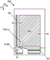


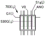


Classifications
-
- H—ELECTRICITY
- H10—SEMICONDUCTOR DEVICES; ELECTRIC SOLID-STATE DEVICES NOT OTHERWISE PROVIDED FOR
- H10K—ORGANIC ELECTRIC SOLID-STATE DEVICES
- H10K50/00—Organic light-emitting devices
- H10K50/80—Constructional details
- H10K50/85—Arrangements for extracting light from the devices
- H10K50/858—Arrangements for extracting light from the devices comprising refractive means, e.g. lenses
-
- H—ELECTRICITY
- H10—SEMICONDUCTOR DEVICES; ELECTRIC SOLID-STATE DEVICES NOT OTHERWISE PROVIDED FOR
- H10K—ORGANIC ELECTRIC SOLID-STATE DEVICES
- H10K50/00—Organic light-emitting devices
- H10K50/10—OLEDs or polymer light-emitting diodes [PLED]
- H10K50/11—OLEDs or polymer light-emitting diodes [PLED] characterised by the electroluminescent [EL] layers
-
- H—ELECTRICITY
- H05—ELECTRIC TECHNIQUES NOT OTHERWISE PROVIDED FOR
- H05B—ELECTRIC HEATING; ELECTRIC LIGHT SOURCES NOT OTHERWISE PROVIDED FOR; CIRCUIT ARRANGEMENTS FOR ELECTRIC LIGHT SOURCES, IN GENERAL
- H05B33/00—Electroluminescent light sources
- H05B33/02—Details
-
- H—ELECTRICITY
- H10—SEMICONDUCTOR DEVICES; ELECTRIC SOLID-STATE DEVICES NOT OTHERWISE PROVIDED FOR
- H10K—ORGANIC ELECTRIC SOLID-STATE DEVICES
- H10K50/00—Organic light-emitting devices
- H10K50/10—OLEDs or polymer light-emitting diodes [PLED]
- H10K50/14—Carrier transporting layers
- H10K50/15—Hole transporting layers
- H10K50/156—Hole transporting layers comprising a multilayered structure
-
- H—ELECTRICITY
- H10—SEMICONDUCTOR DEVICES; ELECTRIC SOLID-STATE DEVICES NOT OTHERWISE PROVIDED FOR
- H10K—ORGANIC ELECTRIC SOLID-STATE DEVICES
- H10K50/00—Organic light-emitting devices
- H10K50/10—OLEDs or polymer light-emitting diodes [PLED]
- H10K50/14—Carrier transporting layers
- H10K50/16—Electron transporting layers
- H10K50/166—Electron transporting layers comprising a multilayered structure
-
- H—ELECTRICITY
- H10—SEMICONDUCTOR DEVICES; ELECTRIC SOLID-STATE DEVICES NOT OTHERWISE PROVIDED FOR
- H10K—ORGANIC ELECTRIC SOLID-STATE DEVICES
- H10K50/00—Organic light-emitting devices
- H10K50/10—OLEDs or polymer light-emitting diodes [PLED]
- H10K50/17—Carrier injection layers
-
- H—ELECTRICITY
- H10—SEMICONDUCTOR DEVICES; ELECTRIC SOLID-STATE DEVICES NOT OTHERWISE PROVIDED FOR
- H10K—ORGANIC ELECTRIC SOLID-STATE DEVICES
- H10K50/00—Organic light-emitting devices
- H10K50/80—Constructional details
- H10K50/805—Electrodes
-
- H—ELECTRICITY
- H10—SEMICONDUCTOR DEVICES; ELECTRIC SOLID-STATE DEVICES NOT OTHERWISE PROVIDED FOR
- H10K—ORGANIC ELECTRIC SOLID-STATE DEVICES
- H10K59/00—Integrated devices, or assemblies of multiple devices, comprising at least one organic light-emitting element covered by group H10K50/00
- H10K59/80—Constructional details
- H10K59/805—Electrodes
-
- H—ELECTRICITY
- H10—SEMICONDUCTOR DEVICES; ELECTRIC SOLID-STATE DEVICES NOT OTHERWISE PROVIDED FOR
- H10K—ORGANIC ELECTRIC SOLID-STATE DEVICES
- H10K2101/00—Properties of the organic materials covered by group H10K85/00
- H10K2101/30—Highest occupied molecular orbital [HOMO], lowest unoccupied molecular orbital [LUMO] or Fermi energy values
-
- H—ELECTRICITY
- H10—SEMICONDUCTOR DEVICES; ELECTRIC SOLID-STATE DEVICES NOT OTHERWISE PROVIDED FOR
- H10K—ORGANIC ELECTRIC SOLID-STATE DEVICES
- H10K2101/00—Properties of the organic materials covered by group H10K85/00
- H10K2101/40—Interrelation of parameters between multiple constituent active layers or sublayers, e.g. HOMO values in adjacent layers
Abstract
Provided is a novel light emitting device excellent in convenience, practicality, or reliability. The invention is a light emitting device comprising a first electrode, a second electrode, a cell, and a first layer. The cell is sandwiched between the first electrode and the second electrode, and includes a second layer, a third layer, and a fourth layer. The second layer is sandwiched between the third layer and the fourth layer and contains a light-emitting material. The third layer is sandwiched between the second layer and the second electrode, is in contact with the second layer, and contains the first material and an organometallic complex of an alkali metal or an organometallic complex of an alkaline earth metal. The fourth layer is sandwiched between the first electrode and the second layer and comprises a second material. In addition, the first layer is sandwiched between the first electrode and the cell, and includes a second material and a material having electron acceptors. The second material has a first refractive index of 1.5 to 1.75 inclusive in a wavelength range of 455 to 465nm inclusive, and a HOMO level of-5.7 eV to-5.3 eV inclusive.
Description
Technical Field
One embodiment of the present invention relates to a light emitting device, a functional panel, a light emitting device, a display device, an electronic apparatus, or a lighting device.
Note that one embodiment of the present invention is not limited to the above-described technical field. The technical field of one embodiment of the invention disclosed in the present specification and the like relates to an object, a method, or a manufacturing method. In addition, one embodiment of the present invention relates to a process, a machine, a product, or a composition (composition of matter). More specifically, examples of the technical field of one embodiment of the present invention disclosed in the present specification include a semiconductor device, a display device, a light-emitting device, a power storage device, a memory device, a driving method of these devices, and a manufacturing method of these devices.
Background
Light emitting devices (organic EL devices) using organic compounds and utilizing Electroluminescence (EL) are very actively put into practical use. In the basic structure of these light-emitting devices, an organic compound layer (EL layer) containing a light-emitting material is sandwiched between a pair of electrodes. By applying a voltage to the element, carriers (holes and electrons) are injected, and light emission from the light emitting material can be obtained by utilizing the recombination energy of the carriers.
Since such a light emitting device is a self-luminous light emitting device, there are advantages in that visibility is higher than that of liquid crystal when used for a pixel of a display, a backlight is not required, and the like. Therefore, the light emitting device is suitable for a flat panel display element. In addition, a display using such a light emitting device can be manufactured to be thin and light, which is also a great advantage. Furthermore, a very high-speed response is also one of the features of the light emitting device.
Further, since the light-emitting layer of such a light-emitting device can be formed continuously in two dimensions, surface light emission can be obtained. Since this is a feature that is difficult to obtain in a point light source typified by an incandescent lamp or a light emitting diode, or a line light source typified by a fluorescent lamp, the light emitting device has high utility value as a surface light source applicable to lighting and the like.
As described above, a display or a lighting device using a light emitting device can be suitably used for various electronic apparatuses, and research and development for pursuing a light emitting device having better characteristics are increasingly active.
The low light extraction efficiency is one of the common problems of the organic EL element. In particular, attenuation due to reflection caused by the difference in refractive index between adjacent layers becomes a factor of deterioration in element efficiency. In order to reduce the influence, a structure in which a layer made of a low refractive index material is formed inside an EL layer has been proposed (for example, refer to non-patent document 1).
The light emitting device having the structure can have higher light extraction efficiency and external quantum efficiency than the light emitting device having the conventional structure, but it is difficult to form such a low refractive index layer inside the EL layer without adversely affecting important characteristics of other light emitting devices. Because, a low refractive index has a trade-off relationship with high carrier transport property or reliability when used in a light emitting device. This is because the carrier transport property and reliability in an organic compound are mostly derived from the presence of unsaturated bonds, and an organic compound having a very polyunsaturated bond tends to have a high refractive index.
[ Prior Art literature ]
[ patent literature ]
[ patent document 1] Japanese patent application laid-open No. 11-282181
[ non-patent literature ]
[ non-patent document 1] Jaeho Lee, other 12 names, "Synergetic electrode architecture for efficient graphene-based flexible organic light-labeling diodes", nature COMMUNICATIONS, month 6 of 2016, day 2 of DOI:10.1038/ncomms11791
Disclosure of Invention
Technical problem to be solved by the invention
It is an object of one embodiment of the present invention to provide a novel light emitting device excellent in convenience, practicality, or reliability. Further, an object of one embodiment of the present invention is to provide a novel functional panel excellent in convenience, practicality, or reliability. Further, an object of one embodiment of the present invention is to provide a novel light-emitting device excellent in convenience, practicality, or reliability. Further, an object of one embodiment of the present invention is to provide a novel display device excellent in convenience, practicality, or reliability. Further, an object of one embodiment of the present invention is to provide a novel electronic device excellent in convenience, practicality, or reliability. Further, an object of one embodiment of the present invention is to provide a novel lighting device excellent in convenience, practicality, or reliability. Further, it is an object of one embodiment of the present invention to provide a novel light emitting device, a novel functional panel, a novel light emitting device, a novel display device, a novel electronic apparatus, or a novel lighting device.
Note that the description of these objects does not hinder the existence of other objects. Note that one embodiment of the present invention is not required to achieve all of the above objects. Further, the objects other than the above objects are apparent from the descriptions of the specification, drawings, claims, and the like, and the objects other than the above objects can be extracted from the descriptions of the specification, drawings, claims, and the like.
Means for solving the technical problems
(1) In addition, one embodiment of the present invention is a light emitting device including a first electrode, a second electrode, a first unit, and a first layer.
The second electrode has a region overlapping the first electrode, and the first unit has a region sandwiched between the first electrode and the second electrode, and includes a second layer, a third layer, and a fourth layer.
The second layer has a region sandwiched between the third layer and the fourth layer, the second layer comprising a luminescent material. Note that in the description of the present specification, when one layered component has a region sandwiched between two other layers, it can also be said that "the one layered component is sandwiched between the other two layered components".
The third layer has a region sandwiched between the second layer and the second electrode, the third layer is in contact with the second layer, and the third layer contains an organometallic complex of the first material and an alkali metal or an organometallic complex of an alkaline earth metal.
The fourth layer has a region sandwiched between the first electrode and the second layer, and the fourth layer contains the second material HT1.
The first layer has a region sandwiched between the first electrode and the first cell, and the first layer includes a second material HT1 and a material AM having an electron acceptor property.
The second material HT1 has a refractive index n1, and the refractive index n1 is 1.5 to 1.75 within a wavelength range of 455nm to 465 nm.
In addition, the first HOMO level of the second material HT1 is from-5.7 eV to-5.3 eV.
(2) In addition, one embodiment of the present invention is the light emitting device described above, wherein the fourth layer has a first region and a second region.
The first region contains the second material HT1, the second region has a portion sandwiched between the second layer and the first region, and the second region contains the third material HT2.
The third material HT2 has a second HOMO level that is within a range of-0.2 eV or more and 0eV or less of the first HOMO level.
(3) In addition, one embodiment of the present invention is the light-emitting device described above, wherein the first material has a refractive index n2. The refractive index n2 is 1.5 to 1.75 in a wavelength range of 455nm to 465 nm.
Thereby, the light emitting efficiency can be improved. In addition, not only high efficiency but also improved reliability can be achieved. As a result, a novel light emitting device excellent in convenience, practicality, and reliability can be provided.
(4) In addition, one embodiment of the present invention is a light emitting device including a first electrode, a second electrode, and a first unit.
The second electrode has a region overlapping the first electrode, and the first unit has a region sandwiched between the first electrode and the second electrode, and includes a first layer, a second layer, and a third layer.
The first layer has a region sandwiched between the second layer and the third layer, and the first layer contains a light-emitting material.
The third layer has a region sandwiched between the first layer and the second electrode, the third layer is in contact with the first layer, and the third layer contains an organometallic complex of a first material and an alkali metal or an organometallic complex of an alkaline earth metal.
The first material has a refractive index n2, and the refractive index n2 is 1.5 to 1.75 in a wavelength range of 455nm to 465 nm.
(5) In addition, an embodiment of the present invention is the light emitting device described above, wherein the light emitting device is formed in a state where the electric field strength [ V/cm ]]600 th square root of (b)A material having an electron mobility of 1X 10 -7 cm 2 above/Vs and 5X 10 -5 cm 2 and/Vs or less.
Thereby, the light emitting efficiency can be improved. In addition, not only high efficiency but also improved reliability can be achieved. As a result, a novel light emitting device excellent in convenience, practicality, and reliability can be provided.
(6) In addition, one embodiment of the present invention is a light emitting device including a second unit and an intermediate layer.
The second cell has a region sandwiched between the intermediate layer and the second electrode.
The intermediate layer has a region sandwiched between the first cell and the second cell, and the intermediate layer has a function of supplying holes to one of the first cell and the second cell and supplying electrons to the other of the first cell and the second cell.
(7) In addition, one embodiment of the present invention is a functional panel including a functional layer and pixels.
The functional layer comprises a pixel circuit, and the pixel comprises the pixel circuit and the light-emitting device.
The first electrode has a region sandwiched between the functional layer and the second electrode, and is electrically connected to the pixel circuit.
Thereby, the light emission of the light emitting device can be controlled using the pixel circuit. In addition, image information may be displayed. As a result, a novel functional panel excellent in convenience, practicality, and reliability can be provided.
(8) In addition, one embodiment of the present invention is the functional panel, wherein the first electrode has a first transmittance, and the second electrode has a second transmittance, and the second transmittance is higher than the first transmittance.
Thereby, light emitted from the light emitting device can be extracted without passing through the functional layer. In addition, light emitted from the light emitting device can be efficiently extracted without shielding.
(9) In addition, one embodiment of the present invention is a functional panel in which the first electrode has a first transmittance and the second electrode has a second transmittance, and the second transmittance is lower than the first transmittance.
(10) Further, one embodiment of the present invention is a light-emitting device including the above light-emitting device and a transistor or a substrate.
(11) In addition, one embodiment of the present invention is a display device including the above light-emitting device and a transistor or a substrate.
(12) Another aspect of the present invention is a lighting device including the above-described light-emitting device and a housing.
(13) Further, one embodiment of the present invention is an electronic device including the display device, and the sensor, the operation button, the speaker, or the microphone.
In the drawings of the present specification, components are classified according to their functions and are shown as block diagrams of blocks independent of each other, but it is difficult to completely divide the components according to their functions in practice, and one component involves a plurality of functions.
In addition, the light-emitting device in this specification includes an image display device using a light-emitting element. In addition, the light emitting device sometimes further includes the following modules: the light emitting element is mounted with a connector such as an anisotropic conductive film or a module of TCP (Tape Carrier Package: tape carrier package); a module provided with a printed wiring board at an end of the TCP; the light emitting element is directly mounted with a module of an IC (integrated circuit) by COG (Chip On Glass) method. Further, the lighting device and the like sometimes include a light emitting device.
Effects of the invention
According to one embodiment of the present invention, a novel light emitting device excellent in convenience, practicality, or reliability can be provided. Further, according to an embodiment of the present invention, a novel functional panel excellent in convenience, practicality, or reliability can be provided. Further, according to one embodiment of the present invention, a novel light-emitting device excellent in convenience, practicality, or reliability can be provided. Further, according to one embodiment of the present invention, a novel display device excellent in convenience, practicality, or reliability can be provided. Further, according to one embodiment of the present invention, a novel electronic device excellent in convenience, practicality, or reliability can be provided. Further, according to one embodiment of the present invention, a novel lighting device excellent in convenience, practicality, or reliability can be provided. Further, according to an embodiment of the present invention, a novel light-emitting device, a novel functional panel, a novel light-emitting device, a novel display device, a novel electronic apparatus, or a novel lighting device can be provided.
Note that the description of these effects does not hinder the existence of other effects. Note that one mode of the present invention is not required to have all of the above effects. Effects other than the above-described effects are apparent from the descriptions of the specification, drawings, claims, and the like, and effects other than the above-described effects can be extracted from the descriptions of the specification, drawings, claims, and the like.
Brief description of the drawings
Fig. 1A and 1B are diagrams illustrating a structure of a light emitting device according to an embodiment.
Fig. 2A and 2B are diagrams illustrating a structure of a light emitting device according to an embodiment.
Fig. 3A and 3B are diagrams illustrating a structure of a functional panel according to an embodiment.
Fig. 4A to 4C are diagrams illustrating the structure of a functional panel according to an embodiment.
Fig. 5 is a circuit diagram illustrating the structure of a functional panel according to an embodiment.
Fig. 6 is a sectional view illustrating the structure of a functional panel according to an embodiment.
Fig. 7A and 7B are sectional views illustrating the structure of a functional panel according to an embodiment.
Fig. 8A and 8B are sectional views illustrating the structure of a functional panel according to an embodiment.
Fig. 9A and 9B are sectional views illustrating the structure of a functional panel according to an embodiment.
Fig. 10A and 10B are a plan view and a cross-sectional view of an active matrix type light emitting device, respectively.
Fig. 11A and 11B are sectional views of an active matrix type light emitting device.
Fig. 12 is a sectional view of an active matrix type light emitting device.
Fig. 13A and 13B are a perspective view and a cross-sectional view of a passive matrix light-emitting device, respectively.
Fig. 14A and 14AB are a cross-sectional view and a top view of the lighting device, respectively.
Fig. 15A, 15B1, 15B2, and 15C are diagrams showing an electronic device.
Fig. 16A to 16C are diagrams showing the electronic apparatus.
Fig. 17 is a diagram showing a lighting device.
Fig. 18 is a diagram showing the lighting device.
Fig. 19 is a diagram showing an in-vehicle display device and a lighting device.
Fig. 20A to 20C are diagrams showing an electronic apparatus.
Fig. 21A to 21C are diagrams illustrating the structure of a light emitting device according to an embodiment.
Fig. 22 is a diagram illustrating wavelength-refractive index characteristics of a light emitting device according to an embodiment.
Fig. 23 is a diagram illustrating current density-luminance characteristics of a light emitting device according to an embodiment.
Fig. 24 is a diagram illustrating luminance-current efficiency characteristics of a light emitting device according to an embodiment.
Fig. 25 is a diagram illustrating voltage-luminance characteristics of a light emitting device according to an embodiment.
Fig. 26 is a diagram illustrating voltage-current characteristics of a light emitting device according to an embodiment.
Fig. 27 is a diagram illustrating luminance-blue index characteristics of a light emitting device according to an embodiment.
Fig. 28 is a diagram illustrating an emission spectrum of a light emitting device according to an embodiment.
Fig. 29 is a diagram illustrating normalized luminance-time variation characteristics of the light emitting device according to the embodiment.
Fig. 30 is a diagram illustrating current density-luminance characteristics of a light emitting device according to an embodiment.
Fig. 31 is a diagram illustrating luminance-current efficiency characteristics of a light emitting device according to an embodiment.
Fig. 32 is a diagram illustrating voltage-luminance characteristics of a light emitting device according to an embodiment.
Fig. 33 is a diagram illustrating voltage-current characteristics of a light emitting device according to an embodiment.
Fig. 34 is a diagram illustrating luminance-external quantum efficiency characteristics of a light emitting device according to an embodiment.
Fig. 35 is a diagram illustrating an emission spectrum of a light emitting device according to an embodiment.
Fig. 36 is a diagram illustrating normalized luminance-time variation characteristics of the light emitting device according to the embodiment.
Modes for carrying out the invention
A light emitting device according to one embodiment of the present invention includes a first electrode, a second electrode, a cell, and a first layer. The cell is sandwiched between the first electrode and the second electrode, and the cell includes a second layer, a third layer, and a fourth layer. The second layer is sandwiched between a third layer and a fourth layer, the second layer contains a light-emitting material, the third layer is sandwiched between the second layer and the second electrode, the third layer is in contact with the second layer, the third layer contains a first material and an organometallic complex of an alkali metal or an organometallic complex of an alkaline earth metal, the fourth layer is sandwiched between the first electrode and the second layer, and the fourth layer contains a second material. In addition, a first layer is sandwiched between the first electrode and the cell, the first layer including a second material and a material having an electron acceptor property. The second material has a first refractive index of 1.5 to 1.75 inclusive in a wavelength range of 455 to 465nm inclusive, and a HOMO level of-5.7 eV to-5.3 eV inclusive.
Thereby, the light emitting efficiency can be improved. In addition, not only high efficiency but also improved reliability can be achieved. As a result, a novel light emitting device excellent in convenience, practicality, and reliability can be provided.
The embodiments will be described in detail with reference to the accompanying drawings. It is noted that the present invention is not limited to the following description, but one of ordinary skill in the art can easily understand the fact that the manner and details thereof can be changed into various forms without departing from the spirit and scope of the present invention. Therefore, the present invention should not be construed as being limited to the description of the embodiments shown below. Note that, in the structure of the invention described below, the same reference numerals are used in common in different drawings to denote the same parts or parts having the same functions, and repetitive description thereof will be omitted.
(embodiment 1)
In this embodiment mode, a structure of a light emitting device 150 according to an embodiment of the present invention will be described with reference to fig. 1.
Fig. 1A is a diagram illustrating a structure of a light emitting device according to an embodiment of the present invention, and fig. 1B is a diagram illustrating a part of the structure of fig. 1A.
< structural example 1 of light-emitting device 150 >
The light-emitting device 150 described in this embodiment mode includes an electrode 551G (i, j), an electrode 552, and an EL layer 553 (see fig. 1A). Electrode 552 has a region overlapping with electrode 551G (i, j). In addition, the EL layer 553 includes a unit 103.
Structural example of element 103
The cell 103 has a region sandwiched between the electrode 551G (i, j) and the electrode 552. Cell 103 includes layer 111, layer 112, and layer 113.
Structural example of layer 111
The layer 111 is preferably arranged in a region where holes and electrons are recombined. Thus, energy generated by carrier recombination can be efficiently emitted as light. In addition, the layer 111 is preferably disposed away from the metal used for the electrode or the like. Therefore, quenching phenomenon caused by the metal used for the electrode and the like can be suppressed.
For example, a fluorescent light-emitting substance, a phosphorescent light-emitting substance, or a substance exhibiting thermally activated delayed fluorescence (TADF: thermally Activated Delayed Fluorescence) may be used for the light-emitting material (also referred to as TADF material). Thereby, energy generated by carrier recombination can be emitted from the light-emitting material as light EL 1.
Structural example 1 of layer 113
For example, a material having electron-transporting property, a material having an anthracene skeleton, a mixed material, or the like can be used for the material ET. In addition, the layer 113 may be referred to as an electron transport layer. Note that a material whose band gap is larger than that of the light-emitting material in the layer 111 is preferably used for the layer 113. Therefore, energy transfer of excitons generated from the layer 111 to the layer 113 can be suppressed.
Structural example 1 of layer 112
A material having hole-transporting property may be used for the layer 112. In addition, the layer 112 may be referred to as a hole transport layer. Note that a material whose band gap is larger than that of the light-emitting material in the layer 111 is preferably used for the layer 112. Therefore, energy transfer of excitons generated from the layer 111 to the layer 112 can be suppressed.
The material HT1 has a refractive index n1, and the refractive index n1 is 1.5 to 1.75 in a wavelength range of 455nm to 465 nm. The refractive index n1 at 633nm is 1.45 to 1.70.
For example, a material having hole-transporting property, in which the ordinary refractive index of light at 633nm, which is used for measurement of refractive index, is 1.45 or more and 1.70 or less, or the ordinary refractive index of light at 1.50 or more and 1.75 or less in the blue light-emitting region (for example, 455nm or more and 465nm or less) can be used for the material HT 1.
Note that when the material has anisotropy, the ordinary refractive index and the extraordinary refractive index are sometimes different. When the measured thin film is in the above state, the ordinary refractive index and the extraordinary refractive index can be calculated by performing an anisotropic analysis, respectively. Note that in this specification, when the measured material has both the ordinary refractive index and the extraordinary refractive index, the ordinary refractive index is used as an index.
[ Material having hole-transporting property ]
As an example of the material having such hole-transporting property, a monoamine compound having a first aromatic group, a second aromatic group, and a third aromatic group, wherein the first aromatic group, the second aromatic group, and the third aromatic group are bonded to the same nitrogen atom, is given.
The monoamine compound is preferably the following compound: the ratio of carbon atoms bonded by sp3 hybridized orbitals relative to the total number of carbon atoms in the molecule is preferably 23% or more and 55% or less, and in passing 1 In the results of H-NMR measurement of the monoamine compound, the integral value of the signal of less than 4ppm exceeds the integral value of the signal of 4ppm or more.
In addition, it is preferable that the monoamine compound has at least one fluorene skeleton, and any one or more of the first aromatic group, the second aromatic group, and the third aromatic group is a fluorene skeleton.
Examples of the material having hole-transporting property include a material having the following general formula (G) h1 1) To (G) h1 4) An organic compound having such a structure.
[ chemical formula 1]

The above formula (G) h1 1) Ar in (1) 1 Ar and Ar 2 Each independently represents a benzene ring, or a substituent in which two or three benzene rings are bonded to each other. Note that Ar 1 And Ar is a group 2 One or both of them having one or more hydrocarbon groups of 1 to 12 carbon atoms bonded only by sp3 hybridized orbitals, contained in the bond to Ar 1 Ar and Ar 2 The total number of carbon atoms in all the above hydrocarbon groups is 8 or more and is contained in the group bonded to Ar 1 Or Ar 2 The total number of carbon atoms in all the above hydrocarbon groups is 6 or more. Note that, in the above-mentioned hydrocarbon group, a plurality of straight-chain alkyl groups having 1 to 2 carbon atoms are bonded to Ar 1 Or Ar 2 In the case of (2), the straight-chain alkyl groups may also be bonded to each other to form a ring.
[ chemical formula 2]

The above formula (G) h1 2) Wherein m and r each independently represent 1 or 2, and m+r is 2 or 3. In addition, t represents an integer of 0 to 4, preferably 0. In addition, R 5 Represents hydrogen or a hydrocarbon group having 1 to 3 carbon atoms. Note that the types of substituents, the number of substituents, and the positions of bonds of the two phenylene groups may be the same or different when m is 2, and the types of substituents, the number of substituents, and the positions of bonds of the two phenyl groups may be the same or different when r is 2. In addition, when t is an integer of 2 to 4, a plurality of R 5 Can be identical or different from each other, or R 5 Is bonded to each other to form a ring.
[ chemical formula 3]

The above formula (G) h1 2) (G) h1 3) Wherein n and p each independently represent 1 or 2, and n+p is 2 or 3. In addition, s represents an integer of 0 to 4, preferably 0. In addition, R 4 The number of substituents, the number of substituents and the bond position of the two phenylene groups may be the same or different when n is 2, and the number of substituents, the number of substituents and the bond position of the two phenyl groups may be the same or different when p is 2. In addition, when s is an integer of 2 to 4, a plurality of R 4 May be identical to or different from each other.
[ chemical formula 4]

The above formula (G) h1 2) To (G) h1 4) Wherein R is 10 To R 14 R is R 20 To R 24 Each independently represents hydrogen or a hydrocarbon group having 1 to 12 carbon atoms in which the carbon atoms are bonded only by an sp3 hybridized orbital. R is R 10 To R 14 At least three of (A) and R 20 To R 24 Preferably hydrogen. As the hydrocarbon group having 1 to 12 carbon atoms bonded only by sp3 hybridization orbitals, t-butyl and cyclohexyl groups are preferably used. Thereby, the refractive index of the film containing the organic compound can be reduced. Note that the assumption is made that it is contained in R 10 To R 14 R is R 20 To R 24 The total number of carbon atoms in (C) is 8 or more and is contained in R 10 To R 14 Or R is 20 To R 24 The total number of carbon atoms in (2) is 6 or more. In addition, R may also be 4 、R 10 To R 14 R is R 20 To R 24 Is bonded to each other to form a ring.
In addition, the above general formula (G) h1 1) To (G) h1 4) In which u represents an integer of 0 to 4, preferably 0. When u is an integer of 2 to 4, a plurality of R 3 May be identical to or different from each other. In addition, R 1 、R 2 R is R 3 Each independently represents an alkyl group having 1 to 4 carbon atoms, R 1 R is R 2 Or bonded to each other to form a ring.
In addition, as an example of the material having such hole transporting property, an arylamine compound having at least one aromatic group including first to third benzene rings and at least three alkyl groups can be given. In addition, it is assumed that the first to third benzene rings are bonded in order and that the first benzene ring is directly bonded to nitrogen in the amine.
Note that the first benzene ring may also have a substituted or unsubstituted phenyl group, preferably an unsubstituted phenyl group. The second benzene ring or the third benzene ring may have a phenyl group to which an alkyl group is bonded.
Further, it is assumed that a hydrogen atom is not directly bonded to two or more benzene rings of the first to third benzene rings, and preferably, all carbon atoms at 1-and 3-positions of the benzene rings are bonded to any one of the first to third benzene rings, the phenyl group to which the alkyl group is bonded, the at least three alkyl groups, and the nitrogen atom of the amine.
The arylamine compound preferably further has a second aromatic group. As the second aromatic group, an unsubstituted single ring or a group having a condensed ring of a substituted or unsubstituted tricyclic or lower is preferably used, among which a condensed ring having a substituted or unsubstituted tricyclic or lower and having a ring-forming carbon number of 6 to 13 is more preferably used, and a group having a fluorene ring is further preferably used. In addition, as the second aromatic group, a dimethylfluorenyl group is preferably used.
The arylamine compound preferably further has a third aromatic group. The third aromatic group is a group having one to three substituted or unsubstituted benzene rings.
The above-mentioned at least three alkyl groups are preferably an alkanyl group having 2 to 5 carbon atoms. In addition, the alkyl group bonded to the phenyl group is preferably an alkanyl group having 2 to 5 carbon atoms. In particular, as the alkyl group having 2 to 5 carbon atoms, an alkyl group having 3 to 5 carbon atoms having a branched chain is preferably used, and a tert-butyl group is more preferably used.
Examples of the material having hole-transporting property include a material having the following general formula (G) h2 1) To (G) h2 3) An organic compound having such a structure.
[ chemical formula 5]

The above formula (G) h2 1) Ar in (1) 101 Represents a substituted or unsubstituted benzene ring or two or three substituents which are bonded to each other in a ring.
[ chemical formula 6]

In addition, the above general formula (G) h2 2) Wherein x and y each independently represent 1 or 2, and x+y is 2 or 3. In addition, R 109 Representing carbon atomsAlkyl having a number of 1 to 4, w represents an integer of 0 to 4. In addition, R 141 To R 145 Each independently represents any one of hydrogen, an alkyl group having 1 to 6 carbon atoms, and a cycloalkyl group having 5 to 12 carbon atoms. When w is 2 or more, a plurality of R 109 May be identical to or different from each other. When x is 2, the types of substituents, the number of substituents, and the positions of bonds of the two phenylene groups may be the same or different from each other. In addition, when y is 2, two have R 141 To R 145 The types of substituents and the number of substituents in the phenyl group may be the same or different from each other.
[ chemical formula 7]

Note that the above general formula (G h2 3) Wherein R is 101 To R 105 Each independently represents any one of hydrogen, an alkyl group having 1 to 6 carbon atoms, a cycloalkyl group having 6 to 12 carbon atoms, and a substituted or unsubstituted phenyl group.
In addition, the above general formula (G) h2 1) To (G) h2 3) Wherein R is 106 、R 107 R is R 108 Each independently represents an alkyl group having 1 to 4 carbon atoms, and v represents an integer of 0 to 4. When v is 2 or more, a plurality of R 108 May be identical to or different from each other. In addition, R 111 To R 115 One of them is a substituent represented by the above general formula (g 1), and the others each independently represent any one of hydrogen, an alkyl group having 1 to 6 carbon atoms, and a substituted or unsubstituted phenyl group. In the above general formula (g 1), R 121 To R 125 One of the substituents represented by the above general formula (g 2) is any one of hydrogen, an alkyl group having 1 to 6 carbon atoms, and a phenyl group to which an alkyl group having 1 to 6 carbon atoms is bonded, the others being independently represented. In the above general formula (g 2), R 131 To R 135 Each independently represents hydrogen, an alkyl group having 1 to 6 carbon atoms, and a benzene to which an alkyl group having 1 to 6 carbon atoms is bonded Any one of the bases. In addition, R 111 To R 115 、R 121 To R 125 R is R 131 To R 135 At least three of them are alkyl groups having 1 to 6 carbon atoms, R 111 To R 115 Wherein the substituted or unsubstituted phenyl is 1 or less, R 121 To R 125 R is R 131 To R 135 The phenyl group bonded with an alkyl group having 1 to 6 carbon atoms is 1 or less. In addition, at R 112 R is R 114 、R 122 R is R 124 R is as follows 132 R is R 134 At least one R is a group other than hydrogen in at least two of the three combinations.
Specifically, the following materials can be used for the material having hole-transporting property: n, N-bis (4-cyclohexylphenyl) -N- (9, 9-dimethyl-9H-fluoren-2-yl) amine (abbreviation: dchPAF), N- (4-cyclohexylphenyl) -N- (3 ",5" -di-tert-butyl-1, 1 "-biphenyl-4-yl) -N- (9, 9-dimethyl-9H-fluoren-2-yl) -amine (abbreviated as mmtBuBichPAF), N- (3, 3",5 "-tetra-tert-butyl-1, 1':3',1" -terphenyl-5 ' -yl) -N- (4-cyclohexylphenyl) -9, 9-dimethyl-9H-fluoren-2-amine (abbreviated as mmtBumTPchPAF), N- [ (3, 3',5' -tert-butyl) -1,1' -biphenyl-5-yl ] -N- (4-cyclohexylphenyl) -9, 9-dimethyl-9H-fluoren-2-amine (abbreviated as mmtbumbibichpaf), N- (1, 1' -biphenyl-2-yl) -N- [ (3, 3',5' -tri-tert-butyl) -1,1' -biphenyl-5-yl ] -9, 9-dimethyl-9H-fluoren-2-amine (abbreviated as mmtbibutppaf), N- (3, 3',5' -tert-butyl) -1,1' -biphenyl-5-yl ] -9H-fluoren-2-amine, 3",5" -tetra-tert-butyl-1, 1':3',1 "-terphenyl-5' -yl) -9, -dimethyl-9H-fluoren-2-amine (abbreviation: mmtBumTPtBuPAF), N- (1, 1' -biphenyl-2-yl) -N- (3, 3",5',5" -tetra-tert-butyl-1, 1':3',1 "-terphenyl-5-yl) -9, 9-dimethyl-9H-fluoren-2-amine (abbreviation: mmtBumTPoFBi-02), N- (4-cyclohexylphenyl) -N- (3, 3",5',5" -tetra-tert-butyl-1, 1':3',1 "-terphenyl-5-yl) -9, 9-dimethyl-9H-fluoren-2-amine (abbreviation: mmtBumTPchPAF-02), N- (1, 1' -biphenyl-2-yl) -N- (3 ",5',5" -tri-tert-butyl-1, 1':3',1 "-terphenyl-5-yl) -9, 9-dimethyl-9H-fluoren-2-amine (abbreviation: mmtBumtpoFBi-03), N- (4-cyclohexylphenyl) -N- (3 ",5',5" -tri-tert-butyl-1, 1':3',1 "-terphenyl-5-yl) -9, 9-dimethyl-9H-fluoren-2-amine (abbreviation: mmtBumTPchPAF-03), and the like.
< structural example 2 of light-emitting device 150 >
In addition, the light emitting device 150 described in this embodiment mode includes the layer 104.
Structural example of layer 104
The material HT1 has a HOMO level HOMO1 (see fig. 1B). For example, a material having a HOMO level of-5.7 eV or more and-5.3 eV or less, and more preferably-5.7 eV or more and-5.35 eV or less, may be used for the material HT1. The HOMO level is the highest occupied molecular orbital (HOMO: highest Occupied Molecular Orbital) level.
Structural example 2 of layer 112
The material HT2 has a HOMO level HOMO2 (see fig. 1B). For example, a material having a HOMO level in a range of-0.2 eV or more and 0eV or less of the HOMO level HOMO1 may be used for the material HT2.
Structural example 2 of layer 113
For example, a material having electron-transporting properties, in which the ordinary refractive index of blue light-emitting region (455 nm or more and 465nm or less) is 1.50 or more and 1.75 or less or the ordinary refractive index of light at 633nm, which is used for measurement of refractive index, is 1.45 or more and 1.70 or less, can be used for material ET.
[ Material having Electron-transporting Property ]
As one of the above-mentioned materials having electron-transporting property, there is mentioned an organic compound having at least one six-membered ring heteroaromatic ring having 1 to 3 nitrogen atoms, including a plurality of aromatic hydrocarbon rings having 6 to 14 ring-forming carbon atoms, at least two of the plurality of aromatic hydrocarbon rings being benzene rings, and containing a plurality of hydrocarbon groups bonded by sp3 hybridization orbitals.
In addition, in such an organic compound, the proportion of the number of carbon atoms bonded by the sp3 hybridized orbital to the total number of carbon atoms in the molecule is preferably 10% or more and 60% or less, more preferably 10% or more and 50% or less. Alternatively, in such organic compounds, the use of 1 The integral value of the signal less than 4ppm as a result of measurement of the organic compound by H-NMR is preferably 1/2 times or more the integral value of the signal of 4ppm or more.
Note that, preferably, all hydrocarbon groups bonded by sp3 hybridization orbitals in the organic compound are bonded to the above-mentioned condensed aromatic hydrocarbon ring having 6 to 14 ring-forming carbon atoms, and LUMO of the organic compound is not distributed on the condensed aromatic hydrocarbon ring.
The organic compound having electron-transporting property is preferably an organic compound represented by the following general formula (G) e1 1) Or (G) e1 2) An organic compound represented by the formula (I).
[ chemical formula 8]

In the general formula, a represents a six-membered ring heteroaryl ring having 1 to 3 nitrogen atoms, and is preferably a pyridine ring, a pyrimidine ring, a pyrazine ring, a pyridazine ring or a triazine ring.
In addition, R 200 Represents hydrogen, an alkyl group having 1 to 6 carbon atoms, an alicyclic group having 3 to 10 carbon atoms or a compound represented by the general formula (G) e1 1-1) a substituent represented by formula (I).
In addition, R 201 To R 215 At least one of them is a substituted phenyl group, and the others each independently represent hydrogen or carbon atomAn alkyl group having 1 to 6 carbon atoms, an alicyclic group having 3 to 10 carbon atoms, a substituted or unsubstituted aromatic hydrocarbon group having 6 to 14 ring-forming carbon atoms, or a substituted or unsubstituted pyridyl group. R is R 201 、R 203 、R 205 、R 206 、R 208 、R 210 、R 211 、R 213 R is R 215 Hydrogen is preferred. The above-mentioned phenyl group having a substituent has one or two substituents each independently being an alkyl group having 1 to 6 carbon atoms, an alicyclic group having 3 to 10 carbon atoms or a substituted or unsubstituted aromatic hydrocarbon group having 6 to 14 ring-forming carbon atoms.
Note that the compound represented by the general formula (G e1 1) The organic compound includes a plurality of hydrocarbon groups selected from alkyl groups having 1 to 6 carbon atoms and alicyclic groups having 3 to 10 carbon atoms, and the ratio of the total number of carbon atoms bonded by sp3 hybridization orbitals to the total number of carbon atoms in the molecule is 10% to 60%.
The organic compound having electron-transporting property is preferably an organic compound represented by the following general formula (G) e1 2) An organic compound represented by the formula (I).
[ chemical formula 9]

In the general formula, Q 1 To Q 3 Wherein two or three of the above groups represent N, and Q is as defined above 1 To Q 3 Where two of these are N, the remaining ones represent CH.
In addition, R 201 To R 215 At least one of them is a substituted phenyl group, and the others independently represent hydrogen, an alkyl group having 1 to 6 carbon atoms, an alicyclic group having 3 to 10 carbon atoms, a substituted or unsubstituted aromatic hydrocarbon group having 6 to 14 ring-forming carbon atoms, or a substituted or unsubstituted pyridyl group. R is R 201 、R 203 、R 205 、R 206 、R 208 、R 210 、R 211 、R 213 R is R 215 Hydrogen is preferred. The phenyl group having a substituent has one or two substitutionsAnd each of the substituents is independently an alkyl group having 1 to 6 carbon atoms, an alicyclic group having 3 to 10 carbon atoms, or a substituted or unsubstituted aromatic hydrocarbon group having 6 to 14 ring-forming carbon atoms.
Note that it is preferable that the compound represented by the general formula (G e1 2) The organic compound includes a plurality of hydrocarbon groups selected from alkyl groups having 1 to 6 carbon atoms and alicyclic groups having 3 to 10 carbon atoms, and the ratio of the number of carbon atoms bonded by sp3 hybridization orbitals to the total number of carbon atoms in the molecule is 10% or more and 60% or less.
In addition, in the general formula (G) e1 1) Or (G) e1 2) In the organic compound represented by the formula (G), the phenyl group having a substituent is preferably represented by the following formula e1 1-2) a group represented by the formula.
[ chemical formula 10]

In the formula, α represents a substituted or unsubstituted phenylene group, preferably a meta-substituted phenylene group. In addition, when the meta-substituted phenylene group has one substituent, it is preferable that the substituent is also substituted at the meta-position. The substituent is preferably an alkyl group having 1 to 6 carbon atoms or an alicyclic group having 3 to 10 carbon atoms, more preferably an alkyl group having 1 to 6 carbon atoms, and still more preferably a tert-butyl group.
R 220 Represents an alkyl group having 1 to 6 carbon atoms, an alicyclic group having 3 to 10 carbon atoms or a substituted or unsubstituted aromatic hydrocarbon group having 6 to 14 ring-forming carbon atoms.
In addition, j and k represent 1 to 2. Note that in the case where j is 2, a plurality of α may be the same or different. When k is 2, a plurality of R 220 May be the same or different from each other. R is R 220 Preferably a phenyl group, more preferably a phenyl group having an alkyl group having 1 to 6 carbon atoms or an alicyclic group having 3 to 10 carbon atoms in one or both of the two meta positions. The substituent of the phenyl group in one or both of the two meta positions is more preferably an alkyl group having 1 to 6 carbon atoms, and still more preferably a tert-butyl group 。
Specifically, the following materials can be used for the material having electron-transporting properties: 2- { (3 ',5' -Di-tert-butyl) -1,1 '-biphenyl-3-yl } -4, 6-bis (3, 5-di-tert-butylphenyl) -1,3, 5-triazine (abbreviated as mmtBuBP-dmmtBuPTzn), 2- { (3', 5 '-di-tert-butyl) -1,1' -biphenyl-3-yl } -4, 6-diphenyl-1, 3, 5-triazine (abbreviated as mmtBuBPTzn), 2- (3, 3',5' -tetra-tert-butyl-1, 1':3',1 '-phenyl-5' -yl) -4, 6-diphenyl-1, 3, 5-triazine (abbreviated as mmtButTPTzn), 2- { (3 ',5' -di-tert-butyl) -1,1 '-biphenyl-3-yl } -4, 6-bis (3, 5-di-tert-butylphenyl) -1, 3-pyrimidine (abbreviated as mmtBum), 2- (3, 3',5 '-tetra-tert-butyl-1, 1': 6-diphenyl-3-yl) -4, 6-triazine (abbreviated as mmtButBum), and the like.
Thereby, the light emitting efficiency can be improved. As a result, a novel light emitting device excellent in convenience, practicality, and reliability can be provided.
For example, the following materials may be used for material ET: at electric field strength [ V/cm ]]At 600 square root, electron mobility is 1×10 -7 cm 2 above/Vs and 5X 10 -5 cm 2 Materials below/Vs. By suppressing the electron transport property in the electron transport layer, the amount of electron injection into the light emitting layer can be controlled. In addition, the light-emitting layer can be prevented from becoming too many electrons.
Note that this embodiment mode can be appropriately combined with other embodiment modes shown in this specification.
(embodiment 2)
In this embodiment mode, a structure of a light emitting device 150 according to an embodiment of the present invention will be described with reference to fig. 1A.
< structural example of light-emitting device 150 >
The light emitting device 150 includes an electrode 551G (i, j), an electrode 552, and a unit 103.
Structural example of element 103
Structural example 1 of layer 111
Luminescent materials may be used for layer 111.
[ fluorescent substance ]
A fluorescent light-emitting substance may be used for the layer 111. For example, the following fluorescent light-emitting substance can be used for the layer 111. Note that the fluorescent light-emitting substance is not limited thereto, and various known fluorescent light-emitting substances can be used for the layer 111.
In particular, 5, 6-bis [4- (10-phenyl-9-anthryl) phenyl ] can be used]-2,2 '-bipyridine (PAP 2 BPy), 5, 6-bis [4' - (10-phenyl-9-anthryl) biphenyl-4-yl]-2,2' -bipyridine (abbreviated as PAPP2 BPy), N ' -diphenyl-N, N ' -bis [4- (9-phenyl-9H-fluoren-9-yl) phenyl ]]Pyrene-1, 6-diamine (1, 6 FLPAPRN), N '-bis (3-methylphenyl) -N, N' -bis [3- (9-phenyl-9H-fluoren-9-yl) phenyl ] ]Pyrene-1, 6-diamine (1, 6 mMemFLPAPRN), N' -bis [4- (9H-carbazol-9-yl) phenyl ]]-N, N '-diphenylstilbene-4, 4' -diamine (abbreviated as YGA 2S), 4- (9H-carbazol-9-yl) -4'- (10-phenyl-9-anthryl) triphenylamine (abbreviated as YGAPA), 4- (9H-carbazol-9-yl) -4' - (9, 10-diphenyl-2-anthryl) triphenylamine (abbreviated as 2 YGAPA), N, 9-diphenyl-N- [4- (10-phenyl-9-anthryl) phenyl]-9H-carbazol-3-amine (abbreviated PCAPA), perylene, 2,5,8, 11-tetra (t-butyl) perylene (abbreviated TBP), 4- (10-phenyl-9-anthryl) -4'- (9-phenyl-9H-carbazol-3-yl) triphenylamine (abbreviated PCAPA), N' - (2-t-butylanthracene-9, 10-diylbis-4, 1-phenylene) bis [ N, N ', N' -triphenyl-1, 4-phenylenediamine](abbreviated as DPABPA), N, 9-diphenyl-N- [4- (9, 10-diphenyl-2-anthryl) phenyl group]-9H-carbazol-3-amine (abbreviated as 2 PCAPPA), N- [4- (9, 10-diphenyl-2-anthryl) phenyl]-N, N ', N ' -triphenyll-1, 4-phenylenediamine (abbreviated as 2 DPAPPA), N, N, N ', N ', N ", N", N ' "-octaphenyldibenzo [ g, p ]] -2,7, 10, 15-tetramine (DBC 1 for short), coumarin 30, N- (9, 10-diphenyl-2-anthryl) -N, 9-diphenyl-9H-carbazole-3-amine (2 PCAPA for short), N- [9, 10-bis (1, 1' -biphenyl-2-yl) -2-anthryl ]-N, 9-diphenyl-9H-carbazole-3-amine (abbreviation):2 pcappha), N- (9, 10-diphenyl-2-anthryl) -N, N' -triphenyl-1, 4-phenylenediamine (abbreviation: 2 DPAPA), N- [9, 10-bis (1, 1' -biphenyl-2-yl) -2-anthryl]-N, N ', N ' -triphenyll-1, 4-phenylenediamine (abbreviated as: 2 DPABPhA), 9, 10-bis (1, 1' -biphenyl-2-yl) -N- [4- (9H-carbazol-9-yl) phenyl ]]-N-phenylanthracene-2-amine (abbreviated as 2 YGABAPhA), N, 9-triphenylanthracene-9-amine (abbreviated as DPhAPHA), coumarin 545T, N, N '-diphenylquinacridone (abbreviated as DPqd), rubrene, 5, 12-bis (1, 1' -biphenyl-4-yl) -6, 11-diphenyltetracene (abbreviated as BPT), 2- (2- {2- [4- (dimethylamino) phenyl ]]Vinyl } -6-methyl-4H-pyran-4-ylidene) malononitrile (abbreviation: DCM 1), 2- { 2-methyl-6- [2- (2, 3,6, 7-tetrahydro-1H, 5H-benzo [ ij ]]Quinolizin-9-yl) vinyl]-4H-pyran-4-ylidene } malononitrile (abbreviated as DCM 2), N, N, N ', N' -tetrakis (4-methylphenyl) acenaphthene-5, 11-diamine (abbreviated as p-mPHTD), 7, 14-diphenyl-N, N, N ', N' -tetrakis (4-methylphenyl) acenaphtho [1,2-a]Fluoranthene-3, 10-diamine (abbreviated as p-mPHIFD), 2- { 2-isopropyl-6- [2- (1, 7-tetramethyl-2, 3,6, 7-tetrahydro-1H, 5H-benzo [ ij ] ]Quinolizin-9-yl) vinyl]-4H-pyran-4-ylidene } malononitrile (DCJTI for short), 2- { 2-tert-butyl-6- [2- (1, 7-tetramethyl-2, 3,6, 7-tetrahydro-1H, 5H-benzo [ ij ]]Quinolizin-9-yl) vinyl]-4H-pyran-4-ylidene } malononitrile (DCJTB for short), 2- (2, 6-bis {2- [4- (dimethylamino) phenyl }, 2-propanedinitrile]Vinyl } -4H-pyran-4-ylidene) malononitrile (abbreviation: bisDCM), 2- {2, 6-bis [2- (8-methoxy-1, 7-tetramethyl-2, 3,6, 7-tetrahydro-1 h,5 h-benzo [ ij ]]Quinolizin-9-yl) vinyl]-4H-pyran-4-ylidene } malononitrile (BisDCJTM for short), N' - (pyrene-1, 6-diyl) bis [ (6, N-diphenylbenzo [ b ]]Naphtho [1,2-d]Furan) -8-amine](abbreviated as 1,6 BnfAPrn-03), 3, 10-bis [ N- (9-phenyl-9H-carbazol-2-yl) -N-phenylamino ]]Naphtho [2,3-b;6,7-b']Bis-benzofuran (3, 10PCA2Nbf (IV) -02), 3, 10-bis [ N- (dibenzofuran-3-yl) -N-phenylamino]Naphtho [2,3-b;6,7-b']Bis-benzofurans (abbreviated as: 3, 10FrA2Nbf (IV) -02), and the like.
In particular, fused aromatic diamine compounds represented by pyrenediamines such as 1,6flpaprn, 1,6 mmmemflpaprn, 1,6 bnfprn-03 and the like are preferable because they have high hole-trapping properties and good luminous efficiency or reliability.
[ phosphorescent light-emitting substance 1]
In addition, a phosphorescent light-emitting substance may be used for the layer 111. For example, the following phosphorescent light-emitting substance can be used for the layer 111. Note that the phosphorescent light-emitting substance is not limited thereto, and various known phosphorescent light-emitting substances may be used for the layer 111.
Specifically, an organometallic iridium complex having a 4H-triazole skeleton or the like can be used for the layer 111. Specifically, tris {2- [5- (2-methylphenyl) -4- (2, 6-dimethylphenyl) -4H-1,2, 4-triazol-3-yl- κN2 may be used]Phenyl-. Kappa.C } iridium (III) (abbreviated as: [ Ir (mpptz-dmp) ] 3 ]) Tris (5-methyl-3, 4-diphenyl-4H-1, 2, 4-triazole) iridium (III) (abbreviation: [ Ir (Mptz) 3 ]) Tris [4- (3-biphenyl) -5-isopropyl-3-phenyl-4H-1, 2, 4-triazole]Iridium (III) (abbreviated as: [ Ir (iPrtz-3 b) 3 ]) Etc.
In addition, for example, an organometallic iridium complex having a 1H-triazole skeleton or the like can be used. Specifically, tris [ 3-methyl-1- (2-methylphenyl) -5-phenyl-1H-1, 2, 4-triazole can be used]Iridium (III) (abbreviated as: [ Ir (Mptz 1-mp) ] 3 ]) Tris (1-methyl-5-phenyl-3-propyl-1H-1, 2, 4-triazole) iridium (III) (abbreviation: [ Ir (Prptz 1-Me) 3 ]) Etc.
In addition, for example, an organometallic iridium complex having an imidazole skeleton or the like can be used. Specifically, fac-tris [1- (2, 6-diisopropylphenyl) -2-phenyl-1H-imidazole can be used ]Iridium (III) (abbreviated: [ Ir (iPrmi) ] 3 ]) Tris [3- (2, 6-dimethylphenyl) -7-methylimidazo [1,2-f ]]Phenanthridine root (phenanthrinator)]Iridium (III) (abbreviated as: [ Ir (dmpimpt-Me) ] 3 ]) Etc.
In addition, for example, an organometallic iridium complex having a phenylpyridine derivative having an electron withdrawing group as a ligand can be used. Specifically, bis [2- (4 ',6' -difluorophenyl) pyridinium-N, C can be used 2’ ]Iridium (III) tetrakis (1-pyrazole) borate (FIr 6 for short), bis [2- (4 ',6' -difluorophenyl) pyridinato-N, C 2’ ]Iridium (III) picolinate (FIrpic), bis {2- [3',5' -bis (trifluoromethyl) phenyl ]]pyridine-N, C 2’ Iridium (III) picolinate (abbreviation: [ Ir (CF) 3 ppy) 2 (pic)]) Bis [2- (4 ',6' -difluorophenyl) pyridino-N, C 2’ ]Iridium (III) acetylacetonate (abbreviated as FIracac) and the like.
The above-mentioned substance is a compound that emits blue phosphorescence, and is a compound having a peak of an emission wavelength at 440nm to 520 nm.
[ phosphorescent light-emitting substance 2]
In addition, for example, an organometallic iridium complex having a pyrimidine skeleton or the like can be used for the layer 111. Specifically, tris (4-methyl-6-phenylpyrimidinyl) iridium (III) (abbreviated: [ Ir (mppm)) 3 ]) Tris (4-tert-butyl-6-phenylpyrimidinyl) iridium (III) (abbreviation: [ Ir (tBuppm) 3 ]) (acetylacetonato) bis (6-methyl-4-phenylpyrimidino) iridium (III) (abbreviation: [ Ir (mppm) 2 (acac)]) (acetylacetonato) bis (6-t-butyl-4-phenylpyrimidino) iridium (III) (abbreviation: [ Ir (tBuppm) 2 (acac)]) (acetylacetonato) bis [6- (2-norbornyl) -4-phenylpyrimidinyl ]]Iridium (III) (abbreviated as: [ Ir (nbppm) ] 2 (acac)]) (acetylacetonato) bis [ 5-methyl-6- (2-methylphenyl) -4-phenylpyrimidinyl ]]Iridium (III) (abbreviated: [ Ir (mpmppm)) 2 (acac)]) (acetylacetonate) bis (4, 6-diphenylpyrimidinyl) iridium (III) (abbreviation: [ Ir (dppm) 2 (acac)]) Etc.
In addition, for example, an organometallic iridium complex having a pyrazine skeleton or the like can be used. Specifically, (acetylacetonato) bis (3, 5-dimethyl-2-phenylpyrazinyl) iridium (III) (abbreviated as: [ Ir (mppr-Me)) 2 (acac)]) (acetylacetonato) bis (5-isopropyl-3-methyl-2-phenylpyrazinyl) iridium (III) (abbreviation: [ Ir (mppr-iPr) 2 (acac)]) Etc.
In addition, for example, an organometallic iridium complex having a pyridine skeleton or the like can be used. Specifically, tris (2-phenylpyridyl-N, C may be used 2 ' iridium (III) (abbreviation: [ Ir (ppy) 3 ]) Bis (2-phenylpyridyl-N, C) 2 ' iridium (III) acetylacetonate (abbreviation: [ Ir (ppy) 2 (acac)]) Bis (benzo [ h ]]Quinoline) iridium (III) acetylacetonate (abbreviation: [ Ir (bzq) 2 (acac)]) Tris (benzo [ h ]]Quinoline) iridium (III) (abbreviated as:[Ir(bzq) 3 ]) Tris (2-phenylquinoline-N, C 2 ']Iridium (III) (abbreviated as: [ Ir (pq) ] 3 ]) Bis (2-phenylquinoline-N, C) 2 ' iridium (III) acetylacetonate (abbreviation: [ Ir (pq) 2 (acac)]) (2-d 3-methyl- (2-pyridinyl-. Kappa.N) benzofuro [2, 3-b)]Pyridine-kappa C]Bis [2- (5-d 3-methyl-2-pyridinyl- κn2) phenyl- κ]Iridium (III) (abbreviated as: [ Ir (5 mppy-d 3) ] 2 (mbfpypy-d3)]) (2-d 3-methyl- (2-pyridinyl-. Kappa.N) benzofuro [2, 3-b)]Pyridine-kappa C]Bis [2- (2-pyridinyl- κN) phenyl- κC]Iridium (III) (abbreviated as: [ Ir (ppy)) 2 (mbfpypy-d3)]) Etc.
In addition, for example, rare earth metal complexes and the like can be used. Specifically, there may be mentioned tris (acetylacetonate) (Shan Feige-in) terbium (III) (abbreviated as: [ Tb (acac) ] 3 (Phen)]) Etc.
The above-mentioned substances are mainly compounds that emit green phosphorescence and have peaks of light emission wavelength at 500nm to 600 nm. In addition, an organometallic iridium complex having a pyrimidine skeleton is particularly preferable because it has particularly excellent reliability or luminous efficiency.
[ phosphorescent light-emitting substance 3]
In addition, for example, an organometallic iridium complex having a pyrimidine skeleton or the like can be used for the layer 111. Specifically, (diisobutyrylmethane) bis [4, 6-bis (3-methylphenyl) pyrimidinyl can be used ]Iridium (III) (abbreviated as: [ Ir (5 mdppm) ] 2 (dibm)]) Bis [4, 6-bis (3-methylphenyl) pyrimidinyl) (dipivaloylmethane) iridium (III) (abbreviation: [ Ir (5 mdppm) 2 (dpm)]) Bis [4, 6-di (naphthalen-1-yl) pyrimidinyl]Ir (d 1 npm) iridium (III) (abbreviated as: [ Ir (d 1) npm) 2 (dpm)]) Etc.
In addition, for example, an organometallic iridium complex having a pyrazine skeleton or the like can be used. Specifically, (acetylacetonato) bis (2, 3, 5-triphenylpyrazino) iridium (III) (abbreviated: [ Ir (tppr)) 2 (acac)]) Bis (2, 3, 5-triphenylpyrazinyl) (dipivaloylmethane) iridium (III) (abbreviation: [ Ir (tppr) 2 (dpm)]) (acetylacetonate) bis [2, 3-bis (4-fluorophenyl) quinoxaline]Iridium (III) (abbreviated: [ Ir (Fdpq)) 2 (acac)]) Etc.
In addition, examplesFor example, an organometallic iridium complex having a pyridine skeleton or a quinoline skeleton, or the like can be used. Specifically, tris (1-phenylisoquinoline-N, C may be used 2’ ) Iridium (III) (abbreviation: [ Ir (piq) 3 ]) Bis (1-phenylisoquinoline-N, C 2’ ) Iridium (III) acetylacetonate (abbreviation: [ Ir (piq) 2 (acac)]) Etc.
Further, for example, platinum complexes and the like can be used. Specifically, 2,3,7,8,12,13,17, 18-octaethyl-21H, 23H-porphyrin platinum (II) (abbreviated as PtOEP) and the like can be used.
In addition, for example, rare earth metal complexes and the like can be used. Specifically, tris (1, 3-diphenyl-1, 3-propanedione) (Shan Feige in) europium (III) (abbreviated: [ Eu (DBM)) 3 (Phen)]) Tris [1- (2-thenoyl) -3, 3-trifluoroacetone](Shan Feige) europium (III) (abbreviated as [ Eu (TTA)) 3 (Phen)]) Etc.
The above-mentioned substance is a compound that emits red phosphorescence and has a luminescence peak at 600nm to 700 nm. In addition, an organometallic iridium complex having a pyrazine skeleton can obtain red light emission having chromaticity which can be suitably used for a display device.
[ substance exhibiting delayed fluorescence by Thermal Activation (TADF) ]
Various known TADF materials may be used for the light emitting material.
The difference between the energy level of the lowest singlet excited state (S1) and the energy level of the lowest triplet excited state (T1) of the TADF material is small, whereby the TADF material can convert the triplet excitation energy into the singlet excitation energy by the intersystem crossing. Therefore, the triplet excitation energy can be up-converted (up-converted) to the singlet excitation energy (intersystem crossing) by a minute thermal energy and the singlet excited state can be efficiently generated. In addition, the triplet excited state can be converted into luminescence.
An Exciplex (Exciplex) formed by two substances has a function of converting triplet excitation energy into singlet excitation energy due to a very small difference between the S1 energy level and the T1 energy level.
Note that as an index of the T1 level, a phosphorescence spectrum observed at a low temperature (for example, 77K to 10K) may be used. Regarding the TADF material, when the wavelength energy of the extrapolated line obtained by introducing the line at the tail on the short wavelength side of the fluorescence spectrum is at the S1 level and the wavelength energy of the extrapolated line obtained by introducing the line at the tail on the short wavelength side of the phosphorescence spectrum is at the T1 level, the difference between S1 and T1 is preferably 0.3eV or less, more preferably 0.2eV or less.
Further, when a TADF material is used as the light-emitting substance, the S1 energy level of the host material is preferably higher than that of the TADF material. Further, the T1 energy level of the host material is preferably higher than the T1 energy level of the TADF material.
For example, fullerene and its derivatives, acridine and its derivatives, eosin derivatives, and the like can be used for TADF materials. In addition, metal-containing porphyrins containing magnesium (Mg), zinc (Zn), cadmium (Cd), tin (Sn), platinum (Pt), indium (In), palladium (Pd), or the like can be used for TADF materials.
Specifically, a protoporphyrin-tin fluoride complex (SnF) represented by the following structural formula can be used 2 (protoIX)), mesoporphyrin-tin fluoride complex (SnF) 2 (Meso IX)), hematoporphyrin-tin fluoride complex (SnF) 2 (Hemato IX)), coproporphyrin tetramethyl ester-tin fluoride complex (SnF) 2 (Copro III-4 Me), octaethylporphyrin-tin fluoride Complex (SnF) 2 (OEP)), protoporphyrin-tin fluoride complex (SnF) 2 (Etio I)) and octaethylporphyrin-platinum chloride complex (PtCl) 2 OEP), and the like.
[ chemical formula 11]

In addition, for example, a heterocyclic compound having one or both of a pi-electron rich heteroaromatic ring and a pi-electron deficient heteroaromatic ring may be used for the TADF material.
Specifically, 2- (biphenyl-4-yl) -4, 6-bis (12-phenylindol-2, 3-a ] carbazol-11-yl) -1,3, 5-triazine (abbreviated as PIC-TRZ), 9- (4, 6-diphenyl-1, 3, 5-triazin-2-yl) -9' -phenyl-9H, 9' H-3,3' -dicarbazole (abbreviated as PCCzTzn), 2- {4- [3- (N-phenyl-9H-carbazol-3-yl) -9H-carbazol-9-yl ] phenyl } -4, 6-diphenyl-1, 3, 5-triazine (abbreviated as PCCzPTzn), 2- [4- (10H-phenoxazin-10-yl) phenyl ] -4, 6-diphenyl-1, 3, 5-triazine (abbreviated as PXZ-TRZ), 3- [4- (5-phenyl-5, 10-dihydrophenazin-10-yl) phenyl ] -4, 5-diphenyl-1, 5-dioxazine-1, 9-dioxazine (abbreviated as PCCzPTzn), and (abbreviated as PPRXN-9-methyl-9-dioxazine-9-yl) phenyl ] -4, 6-diphenyl-1, 3, 5-triazine (abbreviated as PCCzPTzn) may be used, 10-dihydroacridine) phenyl ] sulfolane (abbreviation: DMAC-DPS), 10-phenyl-10 h,10' h-spiro [ acridine-9, 9' -anthracene ] -10' -one (abbreviation: ACRSA), and the like.
[ chemical formula 12]

The heterocyclic compound has a pi-electron rich heteroaromatic ring and a pi-electron deficient heteroaromatic ring, and is preferably because of high electron transport property and hole transport property. In particular, among the backbones having a pi electron deficient heteroaromatic ring, a pyridine backbone, a diazine backbone (pyrimidine backbone, pyrazine backbone, pyridazine backbone) and a triazine backbone are preferable because they are stable and have good reliability. In particular, benzofuropyrimidine skeleton, benzothiophenopyrimidine skeleton, benzofuropyrazine skeleton, and benzothiophenopyrazine skeleton are preferable because they have high acceptors and good reliability.
Among the backbones having a pi-electron rich heteroaromatic ring, the acridine backbone, the phenoxazine backbone, the phenothiazine backbone, the furan backbone, the thiophene backbone, and the pyrrole backbone are stable and have good reliability, and therefore, it is preferable to have at least one of the foregoing backbones. The furan skeleton is preferably a dibenzofuran skeleton, and the thiophene skeleton is preferably a dibenzothiophene skeleton. As the pyrrole skeleton, an indole skeleton, a carbazole skeleton, an indole carbazole skeleton, a biscarbazole skeleton, a 3- (9-phenyl-9H-carbazol-3-yl) -9H-carbazole skeleton is particularly preferably used.
Among the materials in which the pi electron-rich heteroaromatic ring and the pi electron-deficient heteroaromatic ring are directly bonded, those in which both the electron donating property of the pi electron-rich heteroaromatic ring and the electron accepting property of the pi electron-deficient heteroaromatic ring are high and the energy difference between the S1 energy level and the T1 energy level is small, and thus thermally activated delayed fluorescence can be obtained efficiently are particularly preferable. In addition, instead of pi-electron deficient heteroaromatic rings, aromatic rings to which electron withdrawing groups such as cyano groups are bonded may be used. Further, as the pi-electron rich skeleton, an aromatic amine skeleton, a phenazine skeleton, or the like can be used.
Examples of the pi electron-deficient skeleton include a xanthene skeleton, thioxanthene dioxide (thioxanthene dioxide) skeleton, oxadiazole skeleton, triazole skeleton, imidazole skeleton, anthraquinone skeleton, boron-containing skeleton such as phenylborane and boran, aromatic or heteroaromatic ring having a nitrile group or a cyano group such as benzonitrile and cyanobenzene, carbonyl skeleton such as benzophenone, phosphine oxide skeleton and sulfone skeleton.
In this way, a pi electron-deficient backbone and a pi electron-rich backbone may be used in place of at least one of the pi electron-deficient heteroaryl ring and the pi electron-rich heteroaryl ring.
Structural example 2 of layer 111
A material having carrier transport property may be used for the host material. For example, a material having a hole-transporting property, a material having an electron-transporting property, a substance exhibiting thermally activated delayed fluorescence, a material having an anthracene skeleton, a mixed material, or the like can be used as the host material.
[ Material having hole-transporting property ]
The material having hole-transporting property preferably has a value of 1×10 -6 cm 2 Hole mobility above/Vs.
In addition, as the material having hole-transporting property, an amine compound or an organic compound having a pi-electron rich heteroaromatic ring skeleton is preferably used. For example, a compound having an aromatic amine skeleton, a compound having a carbazole skeleton, a compound having a thiophene skeleton, a compound having a furan skeleton, or the like can be used.
As the compound having an aromatic amine skeleton, for example, 4 '-bis [ N- (1-naphthyl) -N-phenylamino ] biphenyl (abbreviated as NPB), N' -bis (3-methylphenyl) -N, N '-diphenyl- [1,1' -biphenyl ] -4,4 '-diamine (abbreviated as TPD), 4' -bis [ N- (spiro-9, 9 '-dibenzofuran-2-yl) -N-phenylamino ] biphenyl (abbreviated as BSPB), 4-phenyl-4' - (9-phenylfluoren-9-yl) triphenylamine (abbreviated as BPAFLP), 4-phenyl-3 '- (9-phenylfluoren-9-yl) triphenylamine (abbreviated as mPAFLP), 4-phenyl-4' - (9-phenyl-9H-carbazole-3-yl) triphenylamine (abbreviated as A1 BP), 4 '-diphenyl-4 "- (9-phenyl-9H-carbazole-3-yl) triphenylamine (abbreviated as PCBA1 BP), 4- (1-naphthyl) -4' - (9-phenylfluoren-9-yl) triphenylamine (abbreviated as PCBA) and PCBA (abbreviated as PCBA B, 4 '-bis (1-naphthyl) -4"- (9-phenyl-9H-carbazol-3-yl) triphenylamine (abbreviated as PCBAIB), 9-dimethyl-N-phenyl-N- [4- (9-phenyl-9H-carbazol-3-yl) phenyl ] fluoren-2-amine (abbreviated as PCBAF), N-phenyl-N- [4- (9-phenyl-9H-carbazol-3-yl) phenyl ] spiro-9, 9' -dibenzofuran-2-amine (abbreviated as PCBASF) and the like.
Examples of the compound having a carbazole skeleton include 1, 3-bis (N-carbazolyl) benzene (abbreviated as mCP), 4 '-bis (N-carbazolyl) biphenyl (abbreviated as CBP), 3, 6-bis (3, 5-diphenylphenyl) -9-phenylcarbazole (abbreviated as CzTP), and 3,3' -bis (9-phenyl-9H-carbazole) (abbreviated as PCCP).
As the compound having a thiophene skeleton, for example, 4' - (benzene-1, 3, 5-triyl) tris (dibenzothiophene) (abbreviated as DBT 3P-II), 2, 8-diphenyl-4- [4- (9-phenyl-9H-fluoren-9-yl) phenyl ] dibenzothiophene (abbreviated as DBTFLP-III), 4- [4- (9-phenyl-9H-fluoren-9-yl) phenyl ] -6-phenyldibenzothiophene (abbreviated as DBTFLP-IV) and the like can be used.
As the compound having a furan skeleton, for example, 4' - (benzene-1, 3, 5-triyl) tris (dibenzofuran) (abbreviated as DBF 3P-II), 4- {3- [3- (9-phenyl-9H-fluoren-9-yl) phenyl ] phenyl } dibenzofuran (abbreviated as mmDBFFLBi-II) and the like can be used.
Among them, a compound having an aromatic amine skeleton or a compound having a carbazole skeleton is preferable because it has good reliability and high hole-transporting property and contributes to reduction of driving voltage.
[ Material having Electron-transporting Property ]
As the material having electron-transporting property, a metal complex or an organic compound including a pi-electron deficient heteroaromatic ring skeleton is preferably used. As the organic compound including a pi-electron deficient heteroaromatic ring skeleton, for example, a heterocyclic compound having a polyazole skeleton, a heterocyclic compound having a diazine skeleton, or a heterocyclic compound having a pyridine skeleton can be used. In particular, a heterocyclic compound having a diazine skeleton or a heterocyclic compound having a pyridine skeleton has good reliability, and is therefore preferable. In addition, a heterocyclic compound having a diazine (pyrimidine or pyrazine) skeleton has high electron-transporting property, and the driving voltage can be reduced.
As metal complexes, it is possible to use, for example, bis (10-hydroxybenzo [ h ]]Quinoline) beryllium (II) (abbreviation: beBq 2 ) Bis (2-methyl-8-hydroxyquinoline) (4-phenylphenol) aluminum (III) (abbreviation: BAlq), bis (8-hydroxyquinoline) zinc (II) (abbreviation: znq), bis [2- (2-benzoxazolyl) phenol]Zinc (II) (ZnPBO for short), bis [2- (2-benzothiazolyl) phenol]Zinc (II) (abbreviated as ZnBTZ), and the like.
As the heterocyclic compound having a polyoxazole skeleton, for example, 2- (4-biphenyl) -5- (4-tert-butylphenyl) -1,3, 4-oxadiazole (abbreviated as: PBD), 3- (4-biphenyl) -4-phenyl-5- (4-tert-butylphenyl) -1,2, 4-triazole (abbreviated as: TAZ), 1, 3-bis [5- (p-tert-butylphenyl) -1,3, 4-oxadiazol-2-yl ] benzene (abbreviated as: OXD-7), 9- [4- (5-phenyl-1, 3, 4-oxadiazol-2-yl) phenyl ] -9H-carbazole (abbreviated as: CO 11), 2' - (1, 3, 5-benzenetriyl) tris (1-phenyl-1H-benzimidazole) (abbreviated as: TPBI), 2- [3- (dibenzothiophen-4-yl) phenyl ] -1-phenyl-1H-benzimidazole (abbreviated as: mDBIm-II) and the like can be used.
As the heterocyclic compound having a diazine skeleton, for example, 2- [3- (dibenzothiophen-4-yl) phenyl ] dibenzo [ f, H ] quinoxaline (abbreviated as: 2 mDBTPDBq-II), 2- [3'- (dibenzothiophen-4-yl) biphenyl-3-yl ] dibenzo [ f, H ] quinoxaline (abbreviated as: 2 mDBTBPDBq-II), 2- [3' - (9H-carbazol-9-yl) biphenyl-3-yl ] dibenzo [ f, H ] quinoxaline (abbreviated as: 2 mCzBPDBq), 4, 6-bis [3- (phenanthr-9-yl) phenyl ] pyrimidine (abbreviated as: 4,6 mPnP2Pm), 4, 6-bis [3- (4-dibenzothiophenyl) phenyl ] pyrimidine (abbreviated as: 4,6 mDBTP2Pm-II), 4, 8-bis [3- (dibenzothiophen-4-yl) phenyl ] -benzo [ H ] quinazoline (abbreviated as: 4,8 mPqBqn) and the like can be used.
As the heterocyclic compound having a pyridine skeleton, for example, 3, 5-bis [3- (9H-carbazol-9-yl) phenyl ] pyridine (abbreviated as 35 DCzPPy), 1,3, 5-tris [3- (3-pyridyl) phenyl ] benzene (abbreviated as TmPyPB) and the like can be used.
As the heterocyclic compound having a triazine skeleton, for example, 2- [3'- (9, 9-dimethyl-9H-fluoren-2-yl) -1,1' -biphenyl-3-yl ] -4, 6-diphenyl-1, 3, 5-triazine (abbreviated as mFBPTzn), 2- [ (1, 1 '-biphenyl) -4-yl ] -4-phenyl-6- [9,9' -spirodi (9H-fluoren) -2-yl ] -1,3, 5-triazine (abbreviated as BP-SFTzn), 2- {3- [3- (benzo [ b ] naphtho [1,2-d ] furan-8-yl) phenyl ] phenyl } -4, 6-diphenyl-1, 3, 5-triazine (abbreviated as mBnfBPTzn), 2- {3- [3- (benzo [ b ] naphtho [1,2-d ] furan-6-yl) phenyl ] phenyl } -4, 6-diphenyl-1, 3, 5-triazine (abbreviated as mBnfBPTzn-02) and the like can be used.
[ substance exhibiting delayed fluorescence by Thermal Activation (TADF) ]
Various known TADF materials may be used for the host material.
When a TADF material is used as a host material, triplet excitation energy generated by the TADF material is converted into singlet excitation energy through intersystem crossing and transferred to a light-emitting substance, whereby the light-emitting efficiency of the light-emitting device can be improved. At this time, the TADF material is used as an energy donor, and the light-emitting substance is used as an energy acceptor.
This is very effective when the above-mentioned luminescent substance is a fluorescent luminescent substance. In this case, the S1 energy level of the TADF material is preferably higher than the S1 energy level of the fluorescent substance in order to obtain high luminous efficiency. In addition, the T1 energy level of the TADF material is preferably higher than the S1 energy level of the fluorescent substance. Therefore, the T1 energy level of the TADF material is preferably higher than the T1 energy level of the fluorescent substance.
Furthermore, it is preferable to use a TADF material that exhibits luminescence overlapping with the wavelength of the absorption band on the lowest energy side of the fluorescent light-emitting substance. This is preferable because excitation energy is smoothly transferred from the TADF material to the fluorescent substance, and light emission can be efficiently obtained.
In order to efficiently generate singlet excitation energy from triplet excitation energy through intersystem crossing, recombination of carriers is preferably generated in the TADF material. Further, it is preferable that the triplet excitation energy generated in the TADF material is not transferred to the triplet excitation energy of the fluorescent substance. For this reason, the fluorescent substance preferably has a protecting group around a light-emitting body (skeleton which causes light emission) included in the fluorescent substance. The protecting group is preferably a substituent having no pi bond, preferably a saturated hydrocarbon, specifically, an alkyl group having 3 or more and 10 or less carbon atoms, a substituted or unsubstituted cycloalkyl group having 3 or more and 10 or less carbon atoms, or a trialkylsilyl group having 3 or more and 10 or less carbon atoms, and more preferably a plurality of protecting groups. Substituents having no pi bond have little effect on carrier transport or carrier recombination because of little function of carrier transport, and can distance the TADF material and the luminophore of the fluorescent light-emitting substance from each other.
Here, the light-emitting body refers to an atomic group (skeleton) that causes luminescence in the fluorescent light-emitting substance. The luminophore is preferably a backbone with pi bonds, preferably comprises aromatic rings, and preferably has fused aromatic or fused heteroaromatic rings.
Examples of the condensed aromatic ring or condensed heteroaromatic ring include a phenanthrene skeleton, a stilbene skeleton, an acridone skeleton, a phenoxazine skeleton, a phenothiazine skeleton, and the like. In particular, has a naphthalene skeleton, an anthracene skeleton, a fluorene skeleton, Fluorescent luminescent materials having a skeleton, triphenylene skeleton, naphthacene skeleton, pyrene skeleton, perylene skeleton, coumarin skeleton, quinacridone skeleton, and naphthobisbenzofuran skeleton have high fluorescence quantum yields, and are therefore preferable.
For example, TADF materials that can be used for the light-emitting material may be used for the host material.
[ Material having an anthracene skeleton ]
When a fluorescent light-emitting substance is used as the light-emitting substance, a material having an anthracene skeleton is particularly suitable as a host material. By using a substance having an anthracene skeleton as a host material of a fluorescent light-emitting substance, a light-emitting layer excellent in both light-emitting efficiency and durability can be realized.
Among the substances having an anthracene skeleton used as a host material, substances having a diphenyl anthracene skeleton, particularly a 9, 10-diphenyl anthracene skeleton, are chemically stable, and are therefore preferable.
In addition, when the host material has a carbazole skeleton, hole injection and transport properties are improved, so that it is preferable. In particular, when the host material has a dibenzocarbazole skeleton, the HOMO level thereof is about 0.1eV shallower than carbazole, and not only hole injection is easy but also hole transport property and heat resistance are improved, which is preferable. Therefore, a substance containing a 9, 10-diphenylanthracene skeleton and a carbazole skeleton (or a benzocarbazole skeleton or a dibenzocarbazole skeleton) is suitable as a host material. Note that from the viewpoint of the hole injection/transport property described above, a benzofluorene skeleton or a dibenzofluorene skeleton may be used instead of the carbazole skeleton.
As the substance having an anthracene skeleton, for example, 9-phenyl-3- [4- (10-phenyl-9-anthracenyl) phenyl ] -9H-carbazole (abbreviated as: PCzPA), 3- [4- (1-naphthyl) -phenyl ] -9-phenyl-9H-carbazole (abbreviated as: PCPN), 9- [4- (10-phenyl-9-anthracenyl) phenyl ] -9H-carbazole (abbreviated as: czPA), 7- [4- (10-phenyl-9-anthracenyl) phenyl ] -7H-dibenzo [ c, g ] carbazole (abbreviated as: cgDBCzPA), 6- [3- (9, 10-diphenyl-2-anthracenyl) phenyl ] -benzo [ b ] naphtho [1,2-d ] furan (abbreviated as: 2 mBnfPPA), 9-phenyl-10- {4- (9-phenyl-9H-fluoren-9-yl) biphenyl-4' -yl } anthracene (abbreviated as: FLPPA), 9- (1-naphthyl) -10- [4- (2-naphtyl) phenyl ] anthracene (abbreviated as: nN-. Beta. Anth) and the like can be used.
In particular CzPA, cgDBCzPA, 2mBnfPPA, PCzPA exhibit very good properties.
[ structural example of Mixed Material 1]
In addition, a material in which a plurality of substances are mixed may be used for the host material. For example, a material having electron-transporting property and a material having hole-transporting property may be mixed to be used as the host material. By mixing a material having electron-transporting property and a material having hole-transporting property, adjustment of carrier-transporting property of the layer 111 can be made easier. In addition, the control of the composite region can be performed more easily. The weight ratio of the material having hole-transporting property and the material having electron-transporting property in the mixed material is the material having hole-transporting property: materials with electron transport properties = 1:19 to 19:1.
[ structural example of Mixed Material 2]
In addition, a material mixed with a phosphorescent light emitting substance may be used for the host material. Phosphorescent light-emitting substances can be used as energy donors for supplying excitation energy to fluorescent light-emitting substances when fluorescent light-emitting substances are used as light-emitting substances.
In addition, a mixed material containing an exciplex-forming material may be used for the host material. For example, a material in which the emission spectrum of the formed exciplex overlaps with the wavelength of the absorption band on the lowest energy side of the light-emitting substance can be used for the host material. Therefore, energy transfer can be made smooth, thereby improving luminous efficiency. Alternatively, the driving voltage may be suppressed.
Note that at least one of the materials forming the exciplex may also be a phosphorescent light-emitting substance. Thus, the triplet excitation energy can be efficiently converted into the singlet excitation energy through the intersystem crossing.
Regarding the combination of materials that efficiently form the exciplex, the HOMO level of the material having hole-transporting property is preferably equal to or higher than the HOMO level of the material having electron-transporting property. The LUMO level of the material having hole-transporting property is preferably equal to or higher than the LUMO level of the material having electron-transporting property. Note that the LUMO level and HOMO level of a material can be obtained from electrochemical characteristics (reduction potential and oxidation potential) of the material measured by Cyclic Voltammetry (CV) measurement.
Note that the formation of an exciplex can be confirmed by, for example, the following method: comparing the emission spectrum of a material having hole-transporting property, the emission spectrum of a material having electron-transporting property, and the emission spectrum of a mixed film obtained by mixing these materials, it is explained that an exciplex is formed when a phenomenon is observed in which the emission spectrum of the mixed film shifts to the long wavelength side (or has a new peak on the long wavelength side) than the emission spectrum of each material. Alternatively, when transient Photoluminescence (PL) of a material having hole-transporting property, transient PL of a material having electron-transporting property, and transient PL of a mixed film obtained by mixing these materials are compared, transient PL of the mixed film is observed to have a long lifetime component or a transient response such as a ratio of a delayed component being larger than the transient PL lifetime of each material, the formation of an exciplex is described. In addition, the above-described transient PL may be referred to as transient Electroluminescence (EL). In other words, the formation of an exciplex can be confirmed by observing the difference in transient response from the transient EL of a material having hole-transporting property, the transient EL of a material having electron-transporting property, and the transient EL of a mixed film of these materials.
Structural example 1 of layer 113
A material having electron-transporting property may be used for the layer 113.
[ Material having Electron-transporting Property ]
For example, a material having electron-transporting property that can be used for the layer 111 can be used for the layer 113. Specifically, a material having electron-transporting property that can be used for the host material can be used for the layer 113.
[ Material having an anthracene skeleton ]
In addition, an organic compound having an anthracene skeleton may be used for the layer 113. In particular, an organic compound having both an anthracene skeleton and a heterocyclic skeleton can be suitably used.
For example, an organic compound containing both an anthracene skeleton and a nitrogen-containing five-membered ring skeleton or an organic compound containing both an anthracene skeleton and a nitrogen-containing six-membered ring skeleton may be used. In addition, an organic compound having both a nitrogen-containing five-membered ring skeleton and an anthracene skeleton containing two hetero atoms in the ring or an organic compound having both a nitrogen-containing six-membered ring skeleton and an anthracene skeleton containing two hetero atoms in the ring may be used. Specifically, a pyrazole ring, an imidazole ring, an oxazole ring, a thiazole ring, a pyrazine ring, a pyrimidine ring, a pyridazine ring, or the like can be suitably used for the heterocyclic skeleton.
[ structural example of Mixed Material ]
In addition, a material mixed with a plurality of substances may be used for the layer 113. Specifically, a material mixed with an alkali metal, an alkali metal compound, or an alkali metal complex and a substance having electron-transporting property can be used for the layer 113. For example, as a material having electron-transporting property of the material in which the plural substances are mixed, 2-phenyl-3- {4- [10- (3-pyridyl) -9-anthryl ] phenyl } quinoxaline (abbreviated as: pyA1 PQ) can be used. In particular, when a composite material is used for the layer 104 and the composite material contains a substance having a deep HOMO level of-5.7 eV or more and-5.4 eV or less, the above material can be suitably used for the layer 113. The HOMO level of the material having electron-transporting properties is more preferably-6.0 eV or more. Thereby, the reliability of the light emitting device can be improved.
The metal complex preferably has an 8-hydroxyquinoline structure, for example. Note that when having an 8-hydroxyquinoline structure, a methyl substituent (e.g., a 2-methyl substituent or a 5-methyl substituent) or the like thereof may be used. Specifically, 8-hydroxyquinoline-lithium (abbreviated as Liq), 8-hydroxyquinoline-sodium (abbreviated as Naq), and the like can be used. In particular, among the monovalent metal ion complexes, lithium complexes are preferably used, and Liq is more preferably used.
The alkali metal, the simple substance of the alkali metal, the compound, or the complex is preferably present in such a manner that there is a concentration difference (including the case where the concentration difference is 0) in the thickness direction of the layer 113.
Structural example of layer 112
A material having hole-transporting property may be used for the layer 112.
[ Material having hole-transporting property ]
The material having hole-transporting property preferably has a value of 1×10 -6 cm 2 Hole mobility above/Vs.
For example, a material having hole-transporting property which can be used for the layer 111 can be used for the layer 112. Specifically, a material having hole-transporting property that can be used for the host material can be used for the layer 112.
Note that this embodiment mode can be appropriately combined with other embodiment modes shown in this specification.
In this embodiment mode, a structure of a light emitting device 150 according to an embodiment of the present invention will be described with reference to fig. 1A.
< structural example of light-emitting device 150 >
The light emitting device 150 includes an electrode 551G (i, j), an electrode 552, and a unit 103. In addition, layers 104 and 105 are included.
Structural example of electrode 551G (i, j)
For example, a conductive material may be used for the electrode 551G (i, j). Specifically, a metal, an alloy, a conductive compound, a mixture thereof, or the like may be used for the electrode 551G (i, j). For example, a material having a work function of 4.0eV or more can be suitably used.
For example, indium Tin Oxide (ITO), indium Tin Oxide containing silicon or silicon Oxide, indium zinc Oxide, indium Oxide containing tungsten Oxide and zinc Oxide (IWZO), or the like can be used.
For example, gold (Au), platinum (Pt), nickel (Ni), tungsten (W), chromium (Cr), molybdenum (Mo), iron (Fe), cobalt (Co), copper (Cu), palladium (Pd), or a nitride of a metal material (for example, titanium nitride) may be used. In addition, graphene may be used.
Structural example of layer 104
For example, a material having hole injection property may be used for the layer 104. Specifically, a substance having acceptors and a composite material can be used for the layer 104. In addition, an organic compound and an inorganic compound can be used for a substance having a receptor property. The substance having an acceptor property can extract electrons from the adjacent hole transport layer (or hole transport material) by applying an electric field.
[ example 1 of a Material having hole-injecting Property ]
A substance having an acceptor property can be used for a material having a hole-injecting property. Thus, holes can be easily injected from the electrode 551G (i, j), for example. In addition, the driving voltage of the light emitting device can be reduced.
For example, a compound having an electron withdrawing group (a halogen group or a cyano group) can be used for a substance having an acceptor property. In addition, the organic compound having a receptor property can be easily formed by vapor deposition. Therefore, the productivity of the light emitting device can be improved.
Specifically, 7, 8-tetracyano-2, 3,5, 6-tetrafluoroquinone dimethane (abbreviated as F) 4 -TCNQ), chloranil,2,3,6,7, 10, 11-hexacyanogen-1,4,5,8,9, 12-hexaazatriphenylene (abbreviated as HAT-CN), 1,3,4,5,7, 8-hexafluorotetracyanogen (hexafluoroetracyano) -naphthoquinone dimethane (abbreviated as F6-TCNNQ), 2- (7-dicyanomethylene-1,3,4,5,6,8,9, 10-octafluoro-7H-pyrene-2-subunit) malononitrile, and the like are used for the material having hole injection property.
In particular, a compound in which an electron withdrawing group is bonded to a condensed aromatic ring having a plurality of hetero atoms, such as HAT-CN or the like, is preferable.
In addition, the [3] decenyl derivative comprising an electron withdrawing group (particularly, a halogen group such as a fluoro group or a cyano group) is very high in electron accepting property, and is therefore preferable.
Specifically, α ', α "-1,2, 3-cyclopropanetrimethylene tris [ 4-cyano-2, 3,5, 6-tetrafluorobenzyl cyanide ], α ', α" -1,2, 3-cyclopropanetrimethylene tris [2, 6-dichloro-3, 5-difluoro-4- (trifluoromethyl) benzyl cyanide ], α ', α "-1,2, 3-cyclopropanetrimethylene tris [2,3,4,5, 6-pentafluorophenyl acetonitrile ], and the like can be used.
In addition, molybdenum oxide, vanadium oxide, ruthenium oxide, tungsten oxide, manganese oxide, or the like can be used for a substance having acceptors.
In addition, phthalocyanine complex compounds such as phthalocyanine (abbreviated as H) 2 Pc) or copper phthalocyanine (CuPc), etc.; compounds having an aromatic amine skeleton, e.g. 4,4' -bis [ N- (4-diphenylaminophenyl) -N-phenylamino ]]Biphenyl (DPAB for short), N' -bis {4- [ bis (3-methylphenyl) amino group]Phenyl } -N, N ' -diphenyl- (1, 1' -biphenyl) -4,4' -diamine (abbreviated as DNTPD), and the like.
In addition, a polymer such as poly (3, 4-ethylenedioxythiophene)/poly (styrenesulfonic acid) (abbreviated as PEDOT/PSS) or the like may be used.
[ example 2 of a Material having hole-injecting Property ]
The composite material can be used as a material having hole-transporting property. For example, a composite material containing a substance having an acceptor property in a material having a hole-transporting property can be used. Thus, the material forming the electrode can be selected in a wide range without taking into consideration the work function. As the electrode 551G (i, j), not only a material having a high work function but also a material having a low work function may be used.
Various organic compounds can be used for the material having hole transporting property of the composite material. For example, a compound having an aromatic amine skeleton, a carbazole derivative, an aromatic hydrocarbon, a high molecular compound (oligomer, dendrimer, polymer, or the like), or the like can be used for a material having hole-transporting property of the composite material. Note that a hole mobility of 1×10 can be suitably used - 6 cm 2 Materials above/Vs.
Further, for example, a substance having a deep HOMO level of-5.7 eV or more and-5.4 eV or less can be suitably used for a material having hole-transporting properties of the composite material. Therefore, holes can be easily injected into the hole transport layer. In addition, the reliability of the light emitting device can be improved.
As the compound having an aromatic amine skeleton, for example, N ' -bis (p-tolyl) -N, N ' -diphenyl-p-phenylenediamine (abbreviated as DTDPPA), 4' -bis [ N- (4-diphenylaminophenyl) -N-phenylamino ] biphenyl (abbreviated as DPAB), N ' -bis {4- [ bis (3-methylphenyl) amino ] phenyl } -N, N ' -diphenyl- (1, 1' -biphenyl) -4,4' -diamine (abbreviated as DNTPD), 1,3, 5-tris [ N- (4-diphenylaminophenyl) -N-phenylamino ] benzene (abbreviated as DPA 3B) and the like can be used.
As the carbazole derivative, for example, 3- [ N- (9-phenylcarbazol-3-yl) -N-phenylamino ] -9-phenylcarbazole (abbreviated as PCzPCA 1), 3, 6-bis [ N- (9-phenylcarbazol-3-yl) -N-phenylamino ] -9-phenylcarbazole (abbreviated as PCzPCA 2), 3- [ N- (1-naphthyl) -N- (9-phenylcarbazol-3-yl) amino ] -9-phenylcarbazole (abbreviated as PCzPCN 1), 4' -bis (N-carbazolyl) biphenyl (abbreviated as CBP), 1,3, 5-tris [4- (N-carbazolyl) phenyl ] benzene (abbreviated as TCPB), 9- [4- (N-carbazolyl) ] phenyl-10-phenylanthracene (abbreviated as CzPA), 1, 4-bis [4- (N-carbazolyl) phenyl ] -2,3,5, 6-tetraphenylbenzene and the like can be used.
As the aromatic hydrocarbon, for example, 2-t-butyl-9, 10-bis (2-naphthyl) anthracene (abbreviated as: t-BuDNA), 2-t-butyl-9, 10-bis (1-naphthyl) anthracene (abbreviated as: DPPA), 2-t-butyl-9, 10-bis (4-phenylphenyl) anthracene (abbreviated as: t-BuDBA), 9, 10-bis (2-naphthyl) anthracene (abbreviated as: DNA), 9, 10-diphenyl anthracene (abbreviated as: DPAnth), 2-t-butyl anthracene (abbreviated as: t-BuAnth), 9, 10-bis (4-methyl-1-naphthyl) anthracene (abbreviated as: DMNA), 2-t-butyl-9, 10-bis [2- (1-naphthyl) phenyl ] anthracene, 2,3,6, 7-tetramethyl-9, 10-bis (1-naphthyl) anthracene, 2, 7-bis (4-naphthyl) anthracene, 10-bis (2-t-methyl-1-naphthyl) anthracene, 10-bis (2, 10-diphenyl) anthracene, 10 '-biphenyl-9, 10' -bis (9, 10-diphenyl) anthracene, 6-pentafluorophenyl) phenyl ] -9,9' -dianthracene, anthracene, naphthacene, rubrene, perylene, 2,5,8, 11-tetra (t-butyl) perylene, and the like.
As the aromatic hydrocarbon having a vinyl group, for example, 4' -bis (2, 2-diphenylvinyl) biphenyl (abbreviated as DPVBi), 9, 10-bis [4- (2, 2-diphenylvinyl) phenyl ] anthracene (abbreviated as DPVPA) and the like can be used.
For example, pentacene, coronene, and the like may also be used.
As the polymer compound, for example, poly (N-vinylcarbazole) (abbreviated as PVK), poly (4-vinyltriphenylamine) (abbreviated as PVTPA), poly [ N- (4- { N '- [4- (4-diphenylamino) phenyl ] phenyl-N' -phenylamino } phenyl) methacrylamide ] (abbreviated as PTPDMA), poly [ N, N '-bis (4-butylphenyl) -N, N' -bis (phenyl) benzidine ] (abbreviated as Poly-TPD) and the like can be used.
In addition, for example, a substance having any one of a carbazole skeleton, a dibenzofuran skeleton, a dibenzothiophene skeleton, and an anthracene skeleton can be suitably used for a material having hole-transporting property of the composite material. In addition, a substance containing an aromatic amine having a substituent including a dibenzofuran ring or a dibenzothiophene ring, an aromatic monoamine including a naphthalene ring, or an aromatic monoamine in which a 9-fluorenyl group is bonded to nitrogen of an amine through an arylene group can be used. Note that when a substance including an N, N-bis (4-biphenyl) amino group is used, the reliability of the light-emitting device can be improved.
As the material having hole transporting property of these composite materials, for example, N- (4-biphenyl) -6, N-diphenylbenzo [ b ] naphtho [1,2-d ] furan-8-amine (abbreviated as BnfABP), N-bis (4-biphenyl) -6-phenylbenzo [ b ] naphtho [1,2-d ] furan-8-amine (abbreviated as BBABnf), 4' -bis (6-phenylbenzo [ b ] naphtho [1,2-d ] furan-8-yl) -4 "-phenyltriphenylamine (abbreviated as BnfBB1 BP), N-bis (4-biphenyl) benzo [ b ] naphtho [1,2-d ] furan-6-amine (abbreviated as BBABnf (6)), N-bis (4-biphenyl) benzo [ b ] naphtho [1,2-d ] furan-8-amine (abbreviated as BBnf (8)), N-bis (4-biphenyl) benzo [2, 2-d ] furan-8-amine (abbreviated as BB) and N, N-bis (4-biphenyl) benzo [1,2-d ] furan-6-amine (abbreviated as BB (4-biphenyl) and N, N-bis (4-biphenyl) benzo [1,2-d ] furan-8-amine (abbreviated as BB) may be used, N- [4- (dibenzothiophen-4-yl) phenyl ] -N-phenyl-4-benzidine (abbreviation: thBA1 BP), 4- (2-naphthyl) -4',4 "-diphenyltriphenylamine (abbreviation: bbaβnb), 4- [4- (2-naphthyl) phenyl ] -4',4" -diphenyltriphenylamine (abbreviation: BBAβNBi), 4' -diphenyl-4 "- (6;1 ' -binaphthyl-2-yl) triphenylamine (abbreviated as BBAαNβNB), 4' -diphenyl-4" - (7;1 ' -binaphthyl-2-yl) triphenylamine (abbreviated as BBAαNβNB-03), 4' -diphenyl-4 "- (7-phenyl) naphthalen-2-yl triphenylamine (abbreviated as BBAP βNB-03), 4' -diphenyl-4" - (6;2 ' -binaphthyl-2-yl) triphenylamine (abbreviated as BBA (. Beta.N2) B), 4' -diphenyl-4 "- (7;2 ' -binaphthyl-2-yl) -triphenylamine (abbreviated as BBA (. Beta.N2) B-03), 4,4 '-diphenyl-4 "- (4;2' -binaphthyl-1-yl) triphenylamine (abbreviation: bbaβnαnb), 4 '-diphenyl-4" - (5;2' -binaphthyl-1-yl) triphenylamine (abbreviation: bbaβnαnb-02), 4- (4-biphenyl) -4'- (2-naphthyl) -4 "-phenyltriphenylamine (abbreviated as tpbiaβnb), 4- (3-biphenyl) -4' - [4- (2-naphthyl) phenyl ] -4" -phenyltriphenylamine (abbreviated as mtpbiαnbi), 4- (4-biphenyl) -4'- [4- (2-naphthyl) phenyl ] -4 "-phenyltriphenylamine (abbreviated as tpbiaβnbi), 4-phenyl-4' - (1-naphthyl) triphenylamine (abbreviated as αnba1bp), 4 '-bis (1-naphthyl) triphenylamine (abbreviated as αnbb1bp), 4' -diphenyl-4" - [4'- (carbazol-9-yl) biphenyl-4-yl ] triphenylamine (abbreviated as YGTBi1 BP), 4' - [4- (3-phenyl-9H-carbazol-9-yl) phenyl ] tris (1, 1' -biphenyl-4-yl) amine (abbreviation: YGTBi1 BP-02), 4-diphenyl-4' - (2-naphthyl) -4"- {9- (4-biphenyl) carbazole } triphenylamine (abbreviation: YGTBi βnb), N- [4- (9-phenyl-9H-carbazol-3-yl) phenyl ] -N- [4- (1-naphthyl) phenyl ] -9,9' -spirodi [ 9H-fluoren ] -2-amine (abbreviation: pcnbsf), N-bis (1, 1 '-biphenyl-4-yl) -9,9' -spirodi [ 9H-fluoren ] -2-amine (abbreviation: BBASF), N-bis (1, 1 '-biphenyl-4-yl) -9,9' -spirodi [ 9H-fluoren ] -4-amine (abbreviation: BBASF (4)), N- (1, 1 '-biphenyl-2-yl) -N- (9, 9-dimethyl-9H-fluoren-2-yl) -9,9' -spirodi (9H-fluoren) -4-amine (abbreviation: fbisf), N- (4-biphenyl) -N- (dibenzofuran-4-yl) -9, 9-dimethyl-9H-fluoren-2-amine (abbreviation: frBiF), N- [4- (1-naphthyl) phenyl ] -N- [3- (6-phenyldibenzofuran-4-yl) phenyl ] -1-naphthylamine (abbreviation: mpdbfcbn), 4-phenyl-4' - (9-phenylfluoren-9-yl) triphenylamine (abbreviation: BPAFLP), 4-phenyl-3' - (9-phenylfluoren-9-yl) triphenylamine (abbreviation: mbpfaflp), 4-phenyl-4' - [4- (9-phenylfluoren-9-yl) phenyl ] triphenylamine (abbreviation: BPAFLBi), 4-phenyl-4' - (9-phenyl-9H-carbazol-3-yl) triphenylamine (abbreviation: PCBA1 BP), 4' -diphenyl-4 "- (9-phenyl-9H-carbazol-3-yl) triphenylamine (abbreviation: pcbi 1 BP), 4- (1-naphthyl) -4' - (9-phenyl-9H-carbazol-3-yl) triphenylamine (abbreviation: PCBANB), 4' -bis (1-naphthyl) -4"- (9-phenyl-9H-carbazol-3-yl) triphenylamine (abbreviation: pcnbb), N-phenyl-N- [4- (9-phenyl-9H-carbazol-3-yl) phenyl ] spiro-9, 9' -bifluorene-2-amine (abbreviation: PCBASF), N- (1, 1' -biphenyl-4-yl) -9, 9-dimethyl-N- [4- (9-phenyl-9H-carbazol-3-yl) phenyl ] -9H-fluoren-2-amine (abbreviation: PCBBiF), N-bis (9, 9-dimethyl-9H-fluoren-2-yl) -9,9 '-spirodi-9H-fluoren-4-amine, N-bis (9, 9-dimethyl-9H-fluoren-2-yl) -9,9' -spirodi-9H-fluoren-3-amine, N-bis (9, 9-dimethyl-9H-fluoren-2-yl) -9,9 '-spirodi-9H-fluoren-2-amine, N-bis (9, 9-dimethyl-9H-fluoren-2-yl) -9,9' -spirodi-9H-fluoren-1-amine, and the like.
[ example 3 of a Material having hole-injecting Property ]
A composite material containing a material having hole-transporting property, a substance having acceptor property, and a fluoride of an alkali metal or alkaline earth metal can be used as the material having hole-injecting property. In particular, a composite material having an atomic ratio of fluorine atoms of 20% or more can be suitably used. Thus, the refractive index of layer 104 may be reduced. In addition, a layer having a low refractive index may be formed inside the light emitting device. In addition, external quantum efficiency of the light emitting device can be improved.
Structural example of electrode 552
For example, a conductive material may be used for the electrode 552. Specifically, a metal, an alloy, a conductive compound, a mixture thereof, or the like may be used for the electrode 552. For example, a material having a smaller work function than the electrode 551G (i, j) may be used for the electrode 552. Specifically, a material having a work function of 3.8eV or less can be suitably used.
For example, an element belonging to group 1 of the periodic table, an element belonging to group 2 of the periodic table, a rare earth metal, and an alloy containing the same can be used for the electrode 552.
Specifically, lithium (Li), cesium (Cs), etc., magnesium (Mg), calcium (Ca), strontium (Sr), etc., europium (Eu), ytterbium (Yb), etc., and alloys (MgAg, alLi) containing these may be used for the electrode 552.
Structural example of layer 105
For example, a material having electron-injecting property may be used for the layer 105. Specifically, a substance having donor property is used for the layer 105. In addition, a composite material in which a material having electron-transporting property contains a substance having donor property may be used for the layer 105. Thus, electrons can be easily injected from the electrode 552, for example. In addition, the driving voltage of the light emitting device can be reduced. In addition, various conductive materials may be used for the electrode 552 regardless of the magnitude of the work function. Specifically, al, ag, ITO, indium oxide-tin oxide containing silicon or silicon oxide, or the like can be used for the electrode 552.
[ Material 1 having Electron-injecting properties ]
For example, an alkali metal, an alkaline earth metal, a rare earth metal, or a compound thereof may be used for the substance having donor property. In addition, an organic compound such as tetrathiatetracene (abbreviated as TTN), nickel-dicyanoxide, and nickel-decamethyidicyanoxide can be used for a substance having donor properties.
Specifically, an alkali metal compound (including oxides, halides, carbonates), an alkaline earth metal compound (including oxides, halides, carbonates), or a compound of a rare earth metal (including oxides, halides, carbonates), or the like can be used for the material having electron-injecting property.
Specifically, lithium oxide, lithium fluoride (LiF), cesium fluoride (CsF), and calcium fluoride (CaF) 2 ) Lithium carbonate, cesium carbonate, 8-hydroxyquinoline-lithium (abbreviation: liq) and the like are used for a material having electron-injecting property.
[ Material 2 having Electron-injecting properties ]
For example, a composite material containing an alkali metal, an alkaline earth metal, or a compound thereof and a substance having electron-transporting property can be used as the material having electron-injecting property.
For example, a material having electron-transporting property that can be used for the cell 103 may be used as the material having electron-injecting property.
In addition, a fluoride of an alkali metal in a microcrystalline state or a fluoride of an alkaline earth metal in a microcrystalline state, which contains a substance having an electron-transporting property, may be used as the material having an electron-injecting property.
In particular, a material containing alkali metal fluoride or alkaline earth metal fluoride at a concentration of 50wt% or more can be suitably used. In addition, an organic compound having a bipyridine skeleton may be suitably used. Thus, the refractive index of the layer 105 can be reduced. In addition, external quantum efficiency of the light emitting device can be improved.
[ Material 3 having Electron-injecting properties ]
In addition, an electron compound (electron) can be used for a material having electron-injecting property. For example, a substance in which electrons are added to a mixed oxide of calcium and aluminum at a high concentration, or the like, can be used for a material having electron-injecting properties.
Note that this embodiment mode can be appropriately combined with other embodiment modes shown in this specification.
In this embodiment mode, a structure of a light emitting device 150 according to an embodiment of the present invention will be described with reference to fig. 2A.
Fig. 2A is a sectional view illustrating a structure of a light emitting device according to an embodiment of the present invention, which has a structure different from that shown in fig. 1A.
< structural example of light-emitting device 150 >
The light-emitting device 150 described in this embodiment mode includes the electrode 551G (i, j), the electrode 552, the cell 103, and the intermediate layer 106 (see fig. 2A).
Structural example of intermediate layer 106
The intermediate layer 106 has a region sandwiched between the cell 103 and the electrode 552, and the intermediate layer 106 includes a layer 106A and a layer 106B.
Structural example of layer 106A
For example, a substance having electron-transporting property may be used for the electron relay layer. Therefore, the layer on the anode side contacting the electron relay layer can be separated from the layer on the cathode side contacting the electron relay layer. In addition, the interaction between the layer on the anode side in contact with the electron relay layer and the layer on the cathode side in contact with the electron relay layer can be reduced. Further, electrons can be smoothly transferred to the layer on the anode side in contact with the electron relay layer.
For example, a substance having electron-transporting property can be suitably used for the electron relay layer. Specifically, a substance having a LUMO energy level between a LUMO energy level of a substance having an acceptor property, which is a composite material exemplified by a material having a hole-injecting property, and a LUMO energy level of a substance contained in a layer on a cathode side in contact with the electron-transporting layer can be suitably used for the electron-transporting layer.
For example, a substance having electron-transporting property and having a LUMO level in a range of-5.0 eV or more, preferably-5.0 eV or more and-3.0 eV or less can be used for the electron-transporting layer.
Specifically, a phthalocyanine material can be used for the electronic relay layer. In addition, a metal complex having a metal-oxygen bond and an aromatic ligand may be used for the electron relay layer.
Structural example of layer 106B
For example, layer 106B may be referred to as a charge generation layer. The charge generation layer has a function of supplying electrons to the anode side and supplying holes to the cathode side by applying a voltage. Specifically, electrons may be supplied to the cell 103 arranged on the anode side.
In addition, for example, a composite material exemplified as a material having hole injection property may be used for the charge generation layer. In addition, for example, a stacked film in which a film containing the composite material and a film containing a material having hole-transporting property are stacked may be used for the charge generation layer.
Note that this embodiment mode can be appropriately combined with other embodiment modes shown in this specification.
In this embodiment mode, a structure of a light emitting device 150 according to an embodiment of the present invention will be described with reference to fig. 2B.
Fig. 2B is a cross-sectional view illustrating a structure of a light emitting device according to an embodiment of the present invention, which has a structure different from that shown in fig. 1A and 2A.
< structural example of light-emitting device 150 >
The light-emitting device 150 described in this embodiment mode includes an electrode 551G (i, j), an electrode 552, a cell 103, an intermediate layer 106, and a cell 103 (12) (see fig. 2B). The light emitting device 150 includes the layer 105 (12). In addition, a structure including the intermediate layer 106 and a plurality of cells is sometimes referred to as a stacked light-emitting device or a tandem light-emitting device. Therefore, light emission can be performed at high luminance while keeping the current density low. Furthermore, reliability can be improved. In addition, in the case where the brightness is the same, the driving voltage can be reduced. Further, power consumption can be suppressed.
Structural example of element 103 (12)
The cell 103 (12) has a region sandwiched between the intermediate layer 106 and the electrode 552.
The structures available for the unit 103 may be used for the unit 103 (12). In other words, the light emitting device 150 includes a plurality of stacked units. Note that the plurality of stacked units is not limited to two units, and three or more units may be stacked.
The same structure as that of the unit 103 can be used for the unit 103 (12). In addition, a different structure from that of the unit 103 may be used for the unit 103 (12).
For example, a structure of a light emission color different from that of the unit 103 may be used for the unit 103 (12). Specifically, the red and green light emitting units 103 and the blue light emitting units 103 (12) may be used. Thus, a light emitting device that emits light of a desired color can be provided. Further, for example, a light emitting device that emits white light may be provided.
Structural example of intermediate layer 106
The intermediate layer 106 has a function of supplying electrons to one of the cell 103 and the cell 103 (12) and supplying holes to the other thereof. For example, the intermediate layer 106 described in embodiment 4 can be used.
< method for manufacturing light-emitting device 150 >
For example, each layer of the electrode 551G (i, j), the electrode 552, the unit 103, the intermediate layer 106, and the unit 103 (12) may be formed by a dry method, a wet method, a vapor deposition method, a droplet discharge method, a coating method, a printing method, or the like. In addition, each constituent element may be formed by a different method.
Specifically, the light emitting device 150 can be manufactured using a vacuum evaporation device, an inkjet device, a coating device such as a spin coater or the like, a gravure printing device, an offset printing device, a screen printing device, or the like.
The electrode may be formed by, for example, a wet method or a sol-gel method using a paste of a metal material. Specifically, an indium oxide-zinc oxide film can be formed by a sputtering method using a target material to which zinc oxide is added in an amount of 1 to 20wt% with respect to indium oxide. In addition, an indium oxide (IWZO) film including tungsten oxide and zinc oxide may be formed by a sputtering method using a target material to which 0.5 to 5wt% of tungsten oxide and 0.1 to 1wt% of zinc oxide are added with respect to indium oxide.
Note that this embodiment mode can be appropriately combined with other embodiment modes shown in this specification.
In this embodiment, the structure of a functional panel according to an embodiment of the present invention will be described with reference to fig. 3 to 5.
Fig. 3A is a plan view illustrating a structure of a functional panel according to an embodiment of the present invention, and fig. 3B is a diagram illustrating a part of fig. 3A.
Fig. 4A is a diagram illustrating a portion of fig. 3A. Fig. 4B is a diagram illustrating a portion of fig. 4A, and fig. 4C is a cross-sectional view illustrating another portion of fig. 4A.
Fig. 5 is a circuit diagram illustrating a structure of a pixel circuit of a functional panel usable in one embodiment of the present invention.
< structural example 1 of functional Panel 700 >
The functional panel 700 has an area 231. The region 231 includes a group of pixels 703 (i, j) (refer to fig. 3A).
The functional panel 700 includes a conductive film G1 (i), a conductive film S1G (j), a conductive film ANO, and a conductive film VCOM2 (see fig. 5). In addition, the functional panel 700 includes a conductive film V0.
For example, the conductive film G1 (i) is supplied with the first selection signal, and the conductive film S1G (j) is supplied with the image signal.
Structural example 1> of the pixel 703 (i, j)
A group of pixels 703 (i, j) includes pixels 702G (i, j) (refer to fig. 3B). The pixel 702G (i, j) includes a pixel circuit 530G (i, j) and a light emitting device 550G (i, j) (see fig. 4A and 4B). In addition, a group of pixels 703 (i, j) includes a pixel 702B (i, j), a pixel 702R (i, j), and a pixel 702W (i, j), the pixel 702B (i, j) includes a light emitting device 550B (i, j), and the pixel 702R (i, j) includes a light emitting device 550R (i, j). The pixel 702W (i, j) includes a pixel circuit 530W (i, j) and a light emitting device 550W (i, j) (see fig. 6).
Structural example of the pixel circuit 530G (i, j)
The pixel circuit 530G (i, j) is supplied with a first selection signal, and the pixel circuit 530G (i, j) acquires an image signal according to the first selection signal. For example, the first selection signal may be supplied using the conductive film G1 (i) (refer to fig. 4B). In addition, the conductive film S1g (j) may be used to supply an image signal. Note that the operation of supplying the first selection signal and causing the pixel circuit 530G (i, j) to acquire an image signal may be referred to as "writing".
The pixel circuit 530G (i, j) includes a switch SW21, a transistor M21, a capacitor C22 and a node N21 (see fig. 5). In addition, the pixel circuit 530G (i, j) includes a node N22 and a switch SW23.
The transistor M21 includes a gate electrode electrically connected to the node N21, a first electrode electrically connected to the light emitting device 550G (i, j), and a second electrode electrically connected to the conductive film ANO.
The switch SW21 includes a first terminal electrically connected to the node N21 and a second terminal electrically connected to the conductive film S1G (j), and has a function of controlling a conductive state or a nonconductive state according to the potential of the conductive film G1 (i).
The capacitor C22 includes a conductive film electrically connected to the node N21, and a conductive film electrically connected to the first electrode of the transistor M21.
The switch SW23 includes a first terminal electrically connected to the conductive film V0 and a second terminal electrically connected to the first electrode of the transistor M21, and has a function of controlling a conductive state or a nonconductive state according to the potential of the conductive film G1 (i). A first terminal of the switch SW23 is electrically connected to the node N22.
Thereby, the image signal can be stored in the node N21. In addition, the potential of the node N22 may be initialized using the switch SW23. In addition, the potential of the node N21 may be used to control the intensity of light emitted from the light emitting device 550G (i, j). As a result, a novel functional panel excellent in convenience and reliability can be provided.
Structural example of light-emitting device 550G (i, j)
The light emitting device 550G (i, j) is electrically connected to the pixel circuit 530G (i, j) (see fig. 4A and 5).
The light emitting device 550G (i, j) includes an electrode 551G (i, j) electrically connected to the pixel circuit 530G (i, j), and an electrode 552 electrically connected to the conductive film VCOM2 (see fig. 5 and 7A). In addition, the light emitting device 550G (i, j) has a function of operating according to the potential of the node N21.
For example, an organic electroluminescent element, an inorganic electroluminescent element, a light emitting diode, a QDLED (Quantum Dot LED), or the like may be used for the light emitting device 550G (i, j).
Specifically, the structures described in embodiment modes 1 to 5 can be used for the light-emitting device 550G (i, j).
Structural example 2> of the pixel 703 (i, j)
A plurality of pixels can be used for the pixel 703 (i, j). For example, a plurality of pixels displaying colors of different hues may be used. Note that each of the plurality of pixels may be referred to as a sub-pixel. In addition, a plurality of sub-pixels may be grouped together and may be referred to as a pixel.
Thus, the colors displayed by the plurality of pixels can be additively mixed. In addition, a color of a hue that cannot be displayed by each pixel can be displayed.
Specifically, a pixel 702B (i, j) displaying blue, a pixel 702G (i, j) displaying green, and a pixel 702R (i, j) displaying red may be used for the pixel 703 (i, j). In addition, each of the pixel 702B (i, j), the pixel 702G (i, j), and the pixel 702R (i, j) may be referred to as a sub-pixel (refer to fig. 3B).
For example, the pixel 702W (i, j) for displaying white or the like may be added to the group and used for the pixel 703 (i, j). In addition, a pixel for displaying cyan, a pixel for displaying magenta, and a pixel for displaying yellow may be used for the pixel 703 (i, j).
For example, the above-described group of pixels emitting infrared rays may be added to the pixel 703 (i, j). Specifically, a pixel that emits light including light having a wavelength of 650nm or more and 1000nm or less can be used for the pixel 703 (i, j).
< structural example 2 of functional Panel 700 >
The functional panel described in this embodiment includes a driver circuit GD and a driver circuit SD (see fig. 3A).
Structural example of drive Circuit GD
The driving circuit GD has a function of supplying the first selection signal. For example, the driving circuit GD is electrically connected to the conductive film G1 (i) and supplies the first selection signal.
Structural example of drive Circuit SD
The driving circuit SD is electrically connected to the conductive film S1g (j) and supplies an image signal.
Note that this embodiment mode can be appropriately combined with other embodiment modes shown in this specification.
In this embodiment, a structure of a functional panel according to an embodiment of the present invention will be described with reference to fig. 6 to 8.
Fig. 6 is a diagram illustrating a structure of a functional panel according to an embodiment of the present invention, and is a sectional view taken along the cut lines X1-X2, X3-X4, X9-X10 and a group of pixels 703 (i, j) of fig. 3A.
Fig. 7A is a diagram illustrating a structure of a functional panel according to an embodiment of the present invention, and is a cross-sectional view of a pixel 702G (i, j) shown in fig. 3B. Fig. 7B is a cross-sectional view illustrating a portion of fig. 7A.
Fig. 8A is a view illustrating the structure of a functional panel according to an embodiment of the present invention, and is a sectional view taken along the sectional lines X1-X2 and the sectional lines X3-X4 of fig. 3A. Fig. 8B is a diagram illustrating a portion of fig. 8A.
< structural example 1 of functional Panel 700 >
The functional panel described in this embodiment includes a functional layer 520 (see fig. 6).
Structural example 1 of functional layer 520 >
The functional layer 520 includes pixel circuits 530G (i, j) and pixel circuits 530W (i, j) (see fig. 6). The functional layer 520 includes, for example, a transistor M21 for the pixel circuit 530G (i, j) (see fig. 5 and 7A).
The functional layer 520 includes an opening 591G (i, j). The pixel circuit 530G (i, j) is electrically connected to the light emitting device 550G (i, j) in the opening 591G (i, j) (see fig. 6).
Thus, the pixel circuit 530G (i, j) can be formed in the pixel 702G (i, j). As a result, a novel functional panel excellent in convenience, practicality, and reliability can be provided.
Structural example 2> of functional layer 520
The functional layer 520 includes a driving circuit GD (see fig. 3A and 6). The functional layer 520 includes, for example, a transistor MD for driving the circuit GD (see fig. 6 and 8A).
Thus, for example, the semiconductor film for the driving circuit GD can be formed in the step of forming the semiconductor film for the pixel circuit 530G (i, j). Alternatively, the semiconductor film for the driving circuit GD may be formed using a process different from the process of forming the semiconductor film for the pixel circuit 530G (i, j). Alternatively, the manufacturing process of the functional panel may be simplified. As a result, a novel functional panel excellent in convenience, practicality, and reliability can be provided.
Structural example of transistor
A bottom gate transistor, a top gate transistor, or the like may be used for the functional layer 520. Specifically, a transistor can be used for the switch.
The transistor includes a semiconductor film 508, a conductive film 504, a conductive film 512A, and a conductive film 512B (see fig. 7B).
The semiconductor film 508 includes a region 508A electrically connected to the conductive film 512A and a region 508B electrically connected to the conductive film 512B. The semiconductor film 508 includes a region 508C between the region 508A and the region 508B.
The conductive film 504 includes a region overlapping with the region 508C, and the conductive film 504 functions as a gate electrode.
The insulating film 506 includes a region sandwiched between the semiconductor film 508 and the conductive film 504. The insulating film 506 has a function of a gate insulating film.
The conductive film 512A has one of a function of a source electrode and a function of a drain electrode, and the conductive film 512B has the other of the function of the source electrode and the function of the drain electrode.
In addition, the conductive film 524 can be used for a transistor. The conductive film 524 includes a region sandwiching the semiconductor film 508 between it and the conductive film 504. The conductive film 524 has a function of a second gate electrode.
Structural example 1 of semiconductor film 508 >
For example, a semiconductor containing a group 14 element can be used for the semiconductor film 508. Specifically, a semiconductor containing silicon can be used for the semiconductor film 508.
[ hydrogenated amorphous silicon ]
For example, hydrogenated amorphous silicon may be used for the semiconductor film 508. Alternatively, microcrystalline silicon or the like can be used for the semiconductor film 508. Thus, for example, a functional panel with less display unevenness than a functional panel using polysilicon for the semiconductor film 508 can be provided. Alternatively, the functional panel can be easily enlarged.
[ polycrystalline silicon ]
For example, polysilicon may be used for the semiconductor film 508. Thus, for example, field effect mobility higher than that of a transistor using hydrogenated amorphous silicon for the semiconductor film 508 can be achieved. Alternatively, for example, higher driving capability than a transistor using hydrogenated amorphous silicon for the semiconductor film 508 can be realized. Alternatively, for example, a pixel aperture ratio higher than that of a transistor using hydrogenated amorphous silicon for the semiconductor film 508 can be achieved.
Alternatively, for example, higher reliability than a transistor using hydrogenated amorphous silicon for the semiconductor film 508 can be achieved.
Alternatively, for example, the temperature required for manufacturing a transistor may be lower than that of a transistor using single crystal silicon.
Alternatively, a semiconductor film for a transistor of a driver circuit and a semiconductor film for a transistor of a pixel circuit may be formed in the same step. Alternatively, the driver circuit may be formed over the same substrate as the substrate over which the pixel circuit is formed. Alternatively, the number of components constituting the electronic device may be reduced.
[ monocrystalline silicon ]
For example, single crystal silicon may be used for the semiconductor film 508. Thus, for example, higher definition can be achieved than in a functional panel in which hydrogenated amorphous silicon is used for the semiconductor film 508. For example, a functional panel which shows less unevenness than a functional panel using polysilicon for the semiconductor film 508 can be provided. Alternatively, for example, smart glasses or a head mounted display may be provided.
Structural example 2> of semiconductor film 508
For example, a metal oxide can be used for the semiconductor film 508. Thus, the time for which the pixel circuit can hold an image signal can be prolonged as compared with a pixel circuit using a transistor using amorphous silicon for a semiconductor film. Specifically, the occurrence of flicker can be suppressed, and the selection signal can be supplied at a frequency lower than 30Hz, preferably lower than 1Hz, more preferably lower than 1 time/minute. As a result, eye fatigue of a user of the data processing apparatus can be reduced. In addition, power consumption for driving can be reduced.
For example, a transistor using an oxide semiconductor can be used. Specifically, an oxide semiconductor containing indium, gallium, and zinc, or an oxide semiconductor containing indium, gallium, zinc, and tin can be used for the semiconductor film.
For example, a transistor in which leakage current in an off state is smaller than that of a transistor using amorphous silicon for a semiconductor film can be used. Specifically, a transistor using an oxide semiconductor for a semiconductor film can be used for a switch or the like. Thus, the potential of the floating node can be maintained for a longer period of time than in a circuit in which a transistor using amorphous silicon is used for a switch.
For example, a film containing indium, gallium, and zinc with a thickness of 25nm can be used as the semiconductor film 508.
For example, a conductive film in which a film containing tantalum and nitrogen and a film containing copper and having a thickness of 300nm are stacked can be used as the conductive film 504. Further, the film containing copper includes a region in which a film containing tantalum and nitrogen is sandwiched between the film and the insulating film 506.
For example, a stacked film of a film containing silicon and nitrogen and having a thickness of 400nm and a film containing silicon, oxygen, and nitrogen and having a thickness of 200nm may be used for the insulating film 506. Further, the film containing silicon and nitrogen includes a region in which the film containing silicon, oxygen, and nitrogen is sandwiched between the film containing silicon and the semiconductor film 508.
For example, a conductive film in which a film containing tungsten and having a thickness of 50nm, a film containing aluminum and having a thickness of 400nm, and a film containing titanium and having a thickness of 100nm are stacked in this order can be used as the conductive film 512A or the conductive film 512B. Further, the film containing tungsten includes a region in contact with the semiconductor film 508.
Here, for example, a production line of a bottom gate transistor using amorphous silicon as a semiconductor can be easily modified to a production line of a bottom gate transistor using an oxide semiconductor as a semiconductor. In addition, for example, a production line of a top gate transistor using polysilicon as a semiconductor can be easily modified to a production line of a top gate transistor using an oxide semiconductor as a semiconductor. Which of the above modifications can effectively utilize the existing production line.
This can suppress flickering of the display. In addition, power consumption can be reduced. Alternatively, a moving image with a fast motion can be displayed smoothly. Alternatively, photographs and the like may be displayed in rich gray levels. As a result, a novel functional panel excellent in convenience, practicality, and reliability can be provided.
Structural example 3> of semiconductor film 508
For example, a compound semiconductor can be used for a semiconductor of a transistor. Specifically, a semiconductor containing gallium or arsenic may be used.
For example, an organic semiconductor may be used for the semiconductor of the transistor. Specifically, an organic semiconductor containing polyacenes or graphene can be used for the semiconductor film.
Structural example of capacitor
The capacitor includes one conductive film, another conductive film, and an insulating film. The insulating film includes a region sandwiched between one conductive film and another conductive film.
For example, a conductive film for a source electrode or a drain electrode of a transistor, a conductive film for a gate electrode, an insulating film for a gate insulating film can be used for a capacitor.
Structural example 3> of functional layer 520
The functional layer 520 includes an insulating film 521, an insulating film 518, an insulating film 516, an insulating film 506, an insulating film 501C, and the like (see fig. 7A and 7B).
The insulating film 521 includes a region sandwiched between the pixel circuit 530G (i, j) and the light emitting device 550G (i, j).
The insulating film 518 includes a region sandwiched between the insulating film 521 and the insulating film 501C.
The insulating film 516 includes a region sandwiched between the insulating film 518 and the insulating film 501C.
The insulating film 506 includes a region sandwiched between the insulating film 516 and the insulating film 501C.
[ insulating film 521]
An insulating inorganic material, an insulating organic material, or an insulating composite material containing an inorganic material and an organic material may be used for the insulating film 521.
Specifically, an inorganic oxide film, an inorganic nitride film, an inorganic oxynitride film, or the like, or a stacked material formed by stacking a plurality of films selected from these films can be used for the insulating film 521. For example, a stacked film of the insulating film 521A and the insulating film 521B can be used as the insulating film 521.
For example, a film including a silicon oxide film, a silicon nitride film, a silicon oxynitride film, an aluminum oxide film, or the like, or a stacked material formed by stacking a plurality of materials selected from these films may be used for the insulating film 521. The silicon nitride film is a dense film having an excellent function of suppressing diffusion of impurities.
For example, a polyester, a polyolefin, a polyamide, a polyimide, a polycarbonate, a polysiloxane, an acrylic resin, or the like, or a laminate or a composite of a plurality of resins selected from the above resins may be used for the insulating film 521. Polyimide has better thermal stability, insulation, toughness, low dielectric constant, low thermal expansion rate, chemical resistance and other characteristics than other organic materials. Accordingly, polyimide is particularly preferably used for the insulating film 521 or the like.
The insulating film 521 may be formed using a photosensitive material. Specifically, a film formed using photosensitive polyimide, photosensitive acrylic, or the like can be used for the insulating film 521.
Thus, for example, the insulating film 521 can planarize level differences due to various structures overlapping with the insulating film 521.
[ insulating film 518]
For example, a material which can be used for the insulating film 521 can be used for the insulating film 518.
For example, a material having a function of suppressing diffusion of oxygen, hydrogen, water, an alkali metal, an alkaline earth metal, or the like can be used for the insulating film 518. Specifically, a nitride insulating film may be used for the insulating film 518. For example, silicon nitride, silicon oxynitride, aluminum nitride, aluminum oxynitride, or the like can be used for the insulating film 518. Thereby, diffusion of impurities to the semiconductor film of the transistor can be prevented.
[ insulating film 516]
For example, a material which can be used for the insulating film 521 can be used for the insulating film 516. For example, a stacked film of the insulating film 516A and the insulating film 516B can be used as the insulating film 516.
Specifically, a film whose manufacturing method is different from that of the insulating film 518 can be used for the insulating film 516.
[ insulating film 506]
For example, a material that can be used for the insulating film 521 can be used for the insulating film 506.
Specifically, a film containing a silicon oxide film, a silicon oxynitride film, a silicon nitride oxide film, a silicon nitride film, an aluminum oxide film, a hafnium oxide film, a yttrium oxide film, a zirconium oxide film, a gallium oxide film, a tantalum oxide film, a magnesium oxide film, a lanthanum oxide film, a cerium oxide film, or a neodymium oxide film can be used for the insulating film 506.
[ insulating film 501D ]
The insulating film 501D includes a region sandwiched between the insulating film 501C and the insulating film 516.
For example, a material which can be used for the insulating film 506 can be used for the insulating film 501D.
[ insulating film 501C ]
For example, a material that can be used for the insulating film 521 can be used for the insulating film 501C. Specifically, a material containing silicon and oxygen can be used for the insulating film 501C. Thereby, diffusion of impurities to the pixel circuit, the light emitting device 550G (i, j), and the like can be suppressed.
Structural example 4> of functional layer 520
The functional layer 520 includes a conductive film, wiring, and a terminal. A material having conductivity can be used for wiring, an electrode, a terminal, a conductive film, or the like.
[ Wiring etc. ]
For example, an inorganic conductive material, an organic conductive material, a metal, a conductive ceramic, or the like can be used for wiring or the like.
Specifically, a metal element selected from aluminum, gold, platinum, silver, copper, chromium, tantalum, titanium, molybdenum, tungsten, nickel, iron, cobalt, palladium, or manganese, or the like can be used for wiring or the like. Alternatively, an alloy or the like containing the above metal element may be used for wiring or the like. In particular, alloys of copper and manganese are suitable for micromachining by wet etching.
Specifically, the wiring and the like may take the following structure: a double-layer structure in which a titanium film is laminated on an aluminum film; a double-layer structure in which a titanium film is laminated on a titanium nitride film; a double-layer structure in which a tungsten film is laminated on a titanium nitride film; a double-layer structure in which a tungsten film is laminated on a tantalum nitride film or a tungsten nitride film; a three-layer structure in which a titanium film, an aluminum film, and a titanium film are laminated in this order.
Specifically, a conductive oxide such as indium oxide, indium tin oxide, indium zinc oxide, or zinc oxide to which gallium is added can be used for wiring or the like.
Specifically, a film containing graphene or graphite can be used for wiring or the like.
For example, a film containing graphene oxide may be formed, and then the film containing graphene may be formed by reducing the film containing graphene oxide. The reduction method may be a heating method or a method using a reducing agent.
For example, a film containing metal nanowires can be used for wiring or the like. In particular, metal nanowires comprising silver may be used.
Specifically, a conductive polymer can be used for wiring and the like.
Further, the terminal 519B may be electrically connected to the flexible printed circuit board FPC1 using a conductive material, for example (see fig. 6). Specifically, the terminal 519B may be electrically connected to the flexible printed circuit board FPC1 using, for example, a conductive material CP.
< structural example 2 of functional Panel 700 >
The functional panel 700 includes a substrate 510, a substrate 770, and a sealant 705 (see fig. 7A). In addition, the function panel 700 may include a structure body KB.
A material having light transmittance may be used for the substrate 510 or the substrate 770.
For example, a material having flexibility may be used for the substrate 510 or the substrate 770. Thereby, a functional panel having flexibility can be provided.
For example, a material having a thickness of 0.1mm or more and 0.7mm or less may be used. Specifically, a material polished to a thickness of about 0.1mm can be used. Thereby, the weight can be reduced.
Glass substrates such as the sixth generation (1500 mm×1850 mm), the seventh generation (1870 mm×2200 mm), the eighth generation (2200 mm×2400 mm), the ninth generation (2400 mm×2800 mm), and the tenth generation (2950 mm×3400 mm) may be used for the base material 510 or the base material 770. Thus, a large display device can be manufactured.
An organic material, an inorganic material, a composite material of a mixed organic material and an inorganic material, or the like may be used for the substrate 510 or the substrate 770.
For example, inorganic materials such as glass, ceramics, and metals can be used. Specifically, alkali-free glass, soda lime glass, potash lime glass, crystal glass, aluminosilicate glass, tempered glass, chemically tempered glass, quartz, sapphire, or the like may be used for the substrate 510 or the substrate 770. Alternatively, aluminosilicate glass, tempered glass, chemically tempered glass, sapphire, or the like may be suitably used for the substrate 510 or the substrate 770 disposed on the side close to the user in the functional panel. Thus, damage or injury of the functional panel caused in use can be prevented.
Specifically, an inorganic oxide film, an inorganic nitride film, an inorganic oxynitride film, or the like can be used. For example, a silicon oxide film, a silicon nitride film, a silicon oxynitride film, an aluminum oxide film, or the like can be used. Stainless steel or aluminum, etc. may be used for the substrate 510 or the substrate 770.
For example, a single crystal semiconductor substrate or a polycrystalline semiconductor substrate using silicon or silicon carbide as a material, a compound semiconductor substrate using silicon germanium or the like as a material, an SOI substrate, or the like may be used for the base material 510 or the base material 770. Thus, the semiconductor element can be formed over the substrate 510 or the substrate 770.
For example, an organic material such as a resin, a resin film, or plastic may be used for the substrate 510 or the substrate 770. Specifically, a material containing a resin having siloxane bonds such as polyester, polyolefin, polyamide (nylon, aramid, or the like), polyimide, polycarbonate, polyurethane, acrylic, epoxy, or silicone may be used for the substrate 510 or the substrate 770. For example, a resin film, a resin sheet, a laminate, or the like containing the above resin can be used. Thereby, the weight can be reduced. Alternatively, for example, the occurrence frequency of damage or the like due to dropping can be reduced.
Specifically, polyethylene terephthalate (PET), polyethylene naphthalate (PEN), polyethersulfone (PES), cyclic Olefin Polymer (COP), cyclic Olefin Copolymer (COC), or the like may be used for the substrate 510 or the substrate 770.
For example, a composite material in which a film of a metal plate, a thin glass plate, an inorganic material, or the like is bonded to a resin thin film or the like may be used for the substrate 510 or the substrate 770. For example, a composite material obtained by dispersing a fibrous or particulate metal, glass, an inorganic material, or the like in a resin can be used as the substrate 510 or the substrate 770. For example, a composite material obtained by dispersing a fibrous or particulate resin, an organic material, or the like in an inorganic material can be used as the substrate 510 or the substrate 770.
In addition, a single layer of material or a material in which a plurality of layers are stacked may be used for the substrate 510 or the substrate 770. For example, a material in which an insulating film or the like is laminated can be used. Specifically, a material in which a film of one or more selected from a silicon oxide layer, a silicon nitride layer, a silicon oxynitride layer, and the like is stacked can be used. Thus, for example, diffusion of impurities contained in the base material can be prevented. Alternatively, diffusion of impurities contained in the glass or the resin may be prevented. Alternatively, diffusion of impurities penetrating the resin may be prevented.
In addition, paper, wood, or the like may be used for the substrate 510 or the substrate 770.
For example, a material having heat resistance that can withstand the heat treatment in the manufacturing process may be used for the substrate 510 or the substrate 770. Specifically, a material having resistance to heating in a manufacturing process of directly forming a transistor, a capacitor, or the like can be used for the substrate 510 or the substrate 770.
For example, the following method may be used: for example, an insulating film, a transistor, a capacitor, or the like is formed over a process substrate that is resistant to heating in a manufacturing process, and the formed insulating film, transistor, capacitor, or the like is transferred to the base 510 or the base 770. Thus, for example, an insulating film, a transistor, a capacitor, or the like can be formed over a substrate having flexibility.
< sealant 705>
The sealant 705 includes a region sandwiched between the functional layer 520 and the substrate 770, and has a function of bonding the functional layer 520 and the substrate 770 (see fig. 7A).
An inorganic material, an organic material, or a composite material of an inorganic material and an organic material, or the like may be used for the sealant 705.
For example, an organic material such as a hot melt resin or a cured resin may be used for the sealant 705.
For example, an organic material such as a reaction curable adhesive, a photo curable adhesive, a thermosetting adhesive, or/and an anaerobic adhesive may be used for the sealing agent 705.
Specifically, an adhesive agent containing an epoxy resin, an acrylic resin, a silicone resin, a phenol resin, a polyimide resin, an imine resin, a PVC (polyvinyl chloride) resin, a PVB (polyvinyl butyral) resin, an EVA (ethylene-vinyl acetate) resin, or the like can be used for the sealant 705.
< Structure KB >
The structure KB includes a region sandwiched between the functional layer 520 and the substrate 770. The structure KB has a function of providing a predetermined gap between the functional layer 520 and the substrate 770.
Note that this embodiment mode can be appropriately combined with other embodiment modes shown in this specification.
In this embodiment, a structure of a functional panel according to an embodiment of the present invention will be described with reference to fig. 7.
< structural example 1 of functional Panel 700 >
The functional panel 700 includes light emitting devices 550G (i, j) (refer to fig. 7).
Structural example 1> of light-emitting device 550G (i, j)
The light emitting device 550G (i, j) includes an electrode 551G (i, j), an electrode 552, and a layer 553G (j) containing a light emitting material. Further, the layer 553G (j) containing a light emitting material includes a region sandwiched between the electrode 551G (i, j) and the electrode 552.
[ structural example 1 of layer 553G (j) containing light-emitting Material ]
For example, a stacked material may be used for the layer 553G (j) containing a light-emitting material.
For example, a material that emits blue light, a material that emits green light, or a material that emits red light may be used for the layer 553G (j) containing a light-emitting material. In addition, an infrared ray-emitting material or an ultraviolet ray-emitting material may be used for the layer 553G (j) containing a light-emitting material.
In addition, a stacked material in which a layer containing a fluorescent light-emitting substance and a layer containing a phosphorescent light-emitting substance are stacked may be used for the layer 553G (j) containing a light-emitting material.
Specifically, the structures described in embodiment modes 1 to 5 can be used for the light-emitting device 550G (i, j).
[ structural example 2 of layer 553G (j) containing light-emitting Material ]
For example, a laminate material laminated so as to emit white light may be used for the layer 553G (j) containing a light emitting material.
Specifically, a plurality of materials which emit light having different hues may be used for the layer 553G (j) containing a light-emitting material. For example, a stacked material in which a layer containing a material that emits blue light and a layer containing a material that emits yellow light are stacked may be used for the layer 553G (j) containing a light-emitting material. Alternatively, a stacked material in which a layer containing a material that emits blue light, a layer containing a material that emits red light, and a layer containing a material that emits green light are stacked may be used for the layer 553G (j) containing a light-emitting material.
Note that, for example, the light-emitting device 550G (i, j) may be used overlapping with the coloring film CF (G). Thus, for example, light of a predetermined hue can be extracted from white light.
[ structural example 3 of layer 553G (j) containing light-emitting Material ]
For example, a laminate material laminated so as to emit blue light or ultraviolet light may be used for the layer 553G (j) containing a light emitting material.
In addition, a color conversion layer may be used to overlap with the light emitting device 550G (i, j). Thus, light of a predetermined hue can be extracted from blue light or ultraviolet light, for example.
[ structural example 4 of layer 553G (j) containing light-emitting Material ]
The layer 553G (j) containing a light emitting material includes a light emitting unit. The light emitting unit includes a region in which electrons injected from one side are recombined with holes injected from the other side. In addition, the light emitting unit includes a light emitting material that releases energy generated by recombination of electrons and holes in the form of light.
For example, a plurality of light-emitting units and an intermediate layer may be used for the layer 553G (j) containing a light-emitting material. The intermediate layer includes a region sandwiched between two light emitting units. The intermediate layer has a charge generation region, and is capable of supplying holes to the light emitting cells arranged on the cathode side and electrons to the light emitting cells arranged on the anode side. Note that a structure having a plurality of light emitting units and an intermediate layer is sometimes referred to as a tandem light emitting element.
Thus, the current efficiency of light emission can be improved. Alternatively, the density of the current flowing in the light-emitting element may be reduced at the same luminance. Alternatively, the reliability of the light emitting element can be improved.
For example, a light-emitting unit including a material that emits light of one color phase and a light-emitting unit including a material that emits light of another color phase may be stacked and used for the layer 553G (j) containing a light-emitting material. Alternatively, a light-emitting unit including a material that emits light of one color phase may be stacked and used for the layer 553G (j) containing a light-emitting material. Specifically, two light emitting units including a material that emits blue light may be stacked and used.
For example, a high molecular compound (an oligomer, a dendrimer, a polymer, or the like), a medium molecular compound (a compound between a low molecular and a high molecular, a molecular weight of 400 or more and 4000 or less), or the like may be used for the layer 553G (j) containing a light-emitting material.
[ structural example 1 of electrode 551G (i, j) and electrode 552 ]
For example, a material that can be used for wiring or the like can be used for the electrode 551G (i, j) or the electrode 552. Specifically, a material having transparency to visible light may be used for the electrode 551G (i, j) or the electrode 552.
For example, a conductive oxide or a conductive oxide containing indium, indium oxide, indium tin oxide, indium zinc oxide, zinc oxide to which gallium is added, or the like can be used. Alternatively, a metal film thin so as to transmit light may be used. Alternatively, a material having transparency to visible light may be used.
For example, a metal film that transmits a part of light and reflects the other part of light may be used for the electrode 551G (i, j) or the electrode 552. For example, the distance between the electrode 551G (i, j) and the electrode 552 is adjusted by using the layer 553G (j) containing a light emitting material or the like.
Thus, the light emitting device 550G (i, j) can have a micro resonator structure. Alternatively, light of a specified wavelength can be extracted more efficiently than other light. Alternatively, light with a narrow half-width of the spectrum may be extracted. Alternatively, light of vivid colors may be extracted.
For example, a film that efficiently reflects light may be used for the electrode 551G (i, j) or the electrode 552. Specifically, a material containing silver, palladium, or the like, or a material containing silver, copper, or the like may be used for the metal film.
The electrode 551G (i, j) is electrically connected to the pixel circuit 530G (i, j) in the opening 591G (i, j) (see fig. 7A). The electrode 551G (i, j) overlaps with an opening formed in the insulating film 528, for example, and an insulating film 528 is provided at an edge of the electrode 551G (i, j).
This can prevent the short circuit between the electrode 551G (i, j) and the electrode 552.
[ structural example 2 of electrode 551G (i, j) and electrode 552 ]
The electrode 551G (i, j) has a transmittance T1, and the electrode 552 has a transmittance T2. The transmittance T2 is higher than the transmittance T1.
Thereby, light emitted from the light emitting device 550G (i, j) can be extracted without passing through the functional layer 520. In addition, light emitted from the light emitting device 550G (i, j) can be efficiently extracted without shielding.
< structural example 2 of functional Panel 700 >
The functional panel 700 includes an insulating film 528 and an insulating film 573 (see fig. 7A).
Structural example 1 of insulating film 528-
The insulating film 528 includes a region sandwiched between the functional layer 520 and the substrate 770, and the insulating film 528 includes an opening portion in a region overlapping with the light-emitting device 550G (i, j) (see fig. 7A).
For example, a material which can be used for the insulating film 521 can be used for the insulating film 528. Specifically, a silicon oxide film, a film containing an acrylic resin, a film containing polyimide, or the like can be used for the insulating film 528.
Insulating film 573-
The insulating film 573 includes a region sandwiching the light emitting device 550G (i, j) with the functional layer 520 (see fig. 7A).
For example, one film or a stacked film in which a plurality of films are stacked may be used for the insulating film 573. Specifically, a stacked film of the insulating film 573A which can be formed by a method in which the light-emitting device 550G (i, j) is not easily damaged and the insulating film 573B which has fewer defects and is dense can be used for the insulating film 573. For example, an organic material may be used for the insulating film 573A. In addition, an inorganic material may be used for the insulating film 573B.
Thereby, diffusion of impurities to the light emitting device 550G (i, j) can be suppressed. Alternatively, the reliability of the light emitting device 550G (i, j) may be improved.
< structural example 3 of functional Panel 700 >
The functional panel 700 includes a functional layer 720 (refer to fig. 7A).
< functional layer 720>
The functional layer 720 includes a light shielding film BM, a coloring film CF (G), and an insulating film 771. In addition, a color conversion layer may also be used.
< light shielding film BM >
The light shielding film BM includes an opening in a region overlapping with the pixel 702G (i, j). For example, a dark material may be used for the light shielding film BM. This can improve the contrast of the display.
Coloring film CF (G)
The colored film CF (G) includes a region sandwiched between the substrate 770 and the light-emitting device 550G (i, j). For example, a material that selectively transmits light of a specified color may be used for the colored film CF (G). Specifically, a material that transmits red light, green light, or blue light may be used for the colored film CF (G).
Structural example of insulating film 771
The insulating film 771 includes a region sandwiched between the substrate 770 and the light-emitting device 550G (i, j).
The insulating film 771 includes a region in which the light shielding film BM and the colored film CF (G) are interposed between the substrate 770. This can flatten irregularities due to the thickness of the light shielding film BM and the colored film CF (G).
< color conversion layer >
The color conversion layer includes a region sandwiched between the substrate 770 and the light emitting device 550G (i, j). Alternatively, a region sandwiched between the colored film CF (G) and the light emitting device 550G (i, j) is included.
For example, a material that emits light having a longer wavelength than the incident light may be used for the color conversion layer. For example, a material that absorbs blue light or ultraviolet light and converts it into green light emission, a material that absorbs blue light or ultraviolet light and converts it into red light emission, or a material that absorbs ultraviolet light and converts it into blue light emission may be used for the color conversion layer.
In particular, quantum dots having a diameter of several nm may be used for the color conversion layer. Thereby, light having a half-width spectrum can be emitted. Alternatively, light with high chroma may be emitted.
< structural example 4 of functional Panel 700 >
The functional panel 700 includes a light shielding film KBM (refer to fig. 7A).
< light shielding film KBM >
The light shielding film KBM has an opening in a region overlapping with the pixel 702G (i, j) and an opening in a region overlapping with other pixels adjacent to the pixel 702G (i, j). Further, the light shielding film KBM includes a region sandwiched between the functional layer 520 and the substrate 770 and has a function of providing a specified gap between the functional layer 520 and the substrate 770. For example, a dark material may be used for the light shielding film KBM. Thus, stray light entering from the pixel 702G (i, j) to other adjacent pixels can be suppressed.
< structural example 5 of functional Panel 700 >
The functional panel 700 includes a functional film 770P and the like (see fig. 7A).
The functional film 770P includes a region overlapping with the light emitting device 550G (i, j). The functional film 770P includes a region sandwiching the substrate 770 with the light emitting devices 550G (i, j).
For example, an antireflection film, a polarizing film, a phase difference film, a light diffusion film, a light condensing film, or the like may be used as the functional film 770P.
For example, an antireflection film having a thickness of 1 μm or less may be used for the functional film 770P. Specifically, a laminated film in which 3 or more layers, preferably 5 or more layers, more preferably 15 or more layers of dielectric is laminated may be used for the functional film 770P. Thus, the reflectance can be suppressed to 0.5% or less, preferably 0.08% or less.
For example, a circularly polarizing film may be used for the functional film 770P.
In addition, an antistatic film which suppresses adhesion of dust, a water-proof film which is not easy to adhere dirt, an oil-proof film which is not easy to adhere dirt, an antireflection film (antireflection film), an antiglare film (non-glare film), a hard coat film which suppresses damage during use, a self-repairing film which can repair the damage generated, and the like can be used for the functional film 770P.
< structural example 6 of functional Panel 700 >
The functional panel 700 includes an insulating film 528 and a coloring film CF (G) (see fig. 9A). The functional panel 700 includes a functional layer 520, and the functional layer 520 includes a transistor M21 (see fig. 9A and 9B).
Structural example 2 of insulating film 528
The insulating film 528 includes a region sandwiched between the functional layer 520 and the base 770, and the insulating film 528 includes an opening portion in a region overlapping with the light-emitting device 550W (i, j) (see fig. 9A). In addition, the insulating film 528 includes an opening portion between the light emitting device 550W (i, j) and other light emitting devices adjacent to the light emitting device 550W (i, j). Thereby, light emitted from the light-emitting device 550W (i, j) can be suppressed from being transmitted through the inside of the insulating film 528. Alternatively, stray light entering from the pixel 702W (i, j) to other adjacent pixels may be suppressed.
Structural example of light-emitting device 550W (i, j)
The light-emitting device 550W (i, j) includes an electrode 551W (i, j), an electrode 552, and a layer 553G (j) (see fig. 4C and 9A).
The electrode 551W (i, j) has a transmittance T1. In addition, the electrode 552 has a region overlapping with the electrode 551W (i, j), and has a transmittance T2. The transmittance T1 is higher than the transmittance T2. In addition, the electrode 552 has a higher reflectance than the electrode 551W (i, j).
< structural example of layer 553G (j) >)
Note that, unlike the EL layer 553 described with reference to fig. 2B, the layer 553G (j) includes the cell 103 (13), the layer 105 (13), and the intermediate layer 106 (13) between the intermediate layer 106 and the cell 103 (12). In addition, for example, a structure available for the unit 103 may be used for the unit 103 (13), a structure available for the layer 105 may be used for the layer 105 (13), and a structure available for the intermediate layer 106 may be used for the intermediate layer 106 (13).
The layer 111 has a function of emitting light EL1, the layer 111 (12) has a function of emitting light EL1 (2), the layer 111 (13) has a function of emitting light EL1 (3), and the layer 111 (14) has a function of emitting light EL1 (4).
For example, a light-emitting material that emits blue light may be used for the layer 111 and the layer 111 (12). In addition, for example, a light-emitting material that emits yellow light may be used for the layer 111 (13). In addition, for example, a light-emitting material that emits red light may be used for the layer 111 (14).
Note that this embodiment mode can be appropriately combined with other embodiment modes shown in this specification.
In this embodiment, a light-emitting device using the light-emitting device described in any one of embodiments 1 to 5 will be described.
In this embodiment, a light-emitting device manufactured using the light-emitting device described in any one of embodiments 1 to 5 will be described with reference to fig. 10. Note that fig. 10A is a top view showing the light emitting device, and fig. 10B is a sectional view cut along a-B and C-D in fig. 10A. The light-emitting device includes a driver circuit portion (source line driver circuit 601), a pixel portion 602, and a driver circuit portion (gate line driver circuit 603) which are indicated by dotted lines as means for controlling light emission of the light-emitting device. In addition, reference numeral 604 is a sealing substrate, reference numeral 605 is a sealant, and the inside surrounded by the sealant 605 is a space 607.
Note that the guide wiring 608 is a wiring for transmitting signals input to the source line driver circuit 601 and the gate line driver circuit 603, and receives a video signal, a clock signal, a start signal, a reset signal, and the like from an FPC (flexible printed circuit) 609 serving as an external input terminal. Note that although only an FPC is illustrated here, the FPC may be mounted with a Printed Wiring Board (PWB). The light-emitting device in this specification includes not only a light-emitting device main body but also a light-emitting device mounted with an FPC or a PWB.
Next, a cross-sectional structure is described with reference to fig. 10B. Although a driver circuit portion and a pixel portion are formed over the element substrate 610, one pixel of the source line driver circuit 601 and the pixel portion 602 which are driver circuit portions is shown here.
The element substrate 610 may be a substrate made of glass, quartz, an organic resin, a metal, an alloy, a semiconductor, or the like, or a plastic substrate made of FRP (Fiber Reinforced Plastics: fiber reinforced plastic), PVF (polyvinyl fluoride), polyester, acrylic, or the like.
The structure of the transistor for the pixel or the driving circuit is not particularly limited. For example, an inverted staggered transistor or a staggered transistor may be employed. In addition, either a top gate type transistor or a bottom gate type transistor may be used. The semiconductor material for the transistor is not particularly limited, and for example, silicon, germanium, silicon carbide, gallium nitride, or the like can be used. Or an oxide semiconductor containing at least one of indium, gallium, and zinc, such as an In-Ga-Zn metal oxide, may be used.
The crystallinity of the semiconductor material used for the transistor is not particularly limited, and an amorphous semiconductor or a crystalline semiconductor (a microcrystalline semiconductor, a polycrystalline semiconductor, a single crystal semiconductor, or a semiconductor in which a part thereof has a crystalline region) can be used. It is preferable to use a crystalline semiconductor because deterioration in characteristics of a transistor can be suppressed.
Here, the oxide semiconductor is preferably used for a semiconductor device such as a transistor provided in the above-described pixel or a driver circuit, a transistor used for a touch sensor or the like described later, or the like. Particularly, an oxide semiconductor having a wider band gap than silicon is preferably used. By using an oxide semiconductor having a wider band gap than silicon, off-state current (off-state current) of the transistor can be reduced.
The oxide semiconductor preferably contains at least indium (In) or zinc (Zn). The oxide semiconductor is more preferably an oxide semiconductor including an oxide expressed as an in—m—zn oxide (M is a metal such as Al, ti, ga, ge, Y, zr, sn, la, ce or Hf).
In particular, as the semiconductor layer, the following oxide semiconductor film is preferably used: the semiconductor device has a plurality of crystal portions each having a c-axis oriented in a direction perpendicular to a surface to be formed of the semiconductor layer or a top surface of the semiconductor layer, and no grain boundaries between adjacent crystal portions.
By using the above material for the semiconductor layer, a highly reliable transistor in which variation in electrical characteristics is suppressed can be realized.
In addition, since the off-state current of the transistor having the semiconductor layer is low, the charge stored in the capacitor through the transistor can be held for a long period of time. By using such a transistor for a pixel, the driving circuit can be stopped while maintaining the gradation of an image displayed in each display region. As a result, an electronic device with extremely low power consumption can be realized.
In order to stabilize the characteristics of the transistor, a base film is preferably provided. As the base film, an inorganic insulating film such as a silicon oxide film, a silicon nitride film, a silicon oxynitride film, or a silicon nitride oxide film can be used and manufactured in a single layer or stacked layers. The base film can be formed by a sputtering method, a CVD (Chemical Vapor Deposition: chemical vapor deposition) method (plasma CVD method, thermal CVD method, MOCVD (Metal Organic CVD: organometallic chemical vapor deposition) method, or the like), an ALD (Atomic Layer Deposition: atomic layer deposition) method, a coating method, a printing method, or the like. Note that the base film may be omitted if not required.
Note that the FET623 shows one of transistors formed in the source line driver circuit 601. The driving circuit may be formed using various CMOS circuits, PMOS circuits, or NMOS circuits. In addition, although the driver integrated type driver circuit in which the driver circuit is formed over the substrate is shown in this embodiment mode, this structure is not necessarily required, and the driver circuit may be formed outside rather than over the substrate.
The pixel portion 602 is formed of a plurality of pixels each including the switching FET611, the current control FET612, and the first electrode 613 electrically connected to the drain of the current control FET612, but the present invention is not limited thereto, and a pixel portion in which three or more FETs and capacitors are combined may be employed.
Note that an insulator 614 is formed to cover an end portion of the first electrode 613. Here, the insulator 614 may be formed using a positive type photosensitive acrylic resin film.
In addition, an upper end portion or a lower end portion of the insulator 614 is formed into a curved surface having a curvature to obtain good coverage of an EL layer or the like formed later. For example, in the case where a positive type photosensitive acrylic resin is used as a material of the insulator 614, it is preferable that only an upper end portion of the insulator 614 includes a curved surface having a radius of curvature (0.2 μm or more and 3 μm or less). As the insulator 614, a negative type photosensitive resin or a positive type photosensitive resin can be used.
An EL layer 616 and a second electrode 617 are formed over the first electrode 613. Here, as a material for the first electrode 613 which is used as an anode, a material having a large work function is preferably used. For example, a single-layer film such as an ITO film, an indium tin oxide film containing silicon, an indium oxide film containing zinc oxide of 2wt% or more and 20wt% or less, a titanium nitride film, a chromium film, a tungsten film, a Zn film, a Pt film, or the like, a stacked film composed of a titanium nitride film and a film containing aluminum as a main component, a three-layer structure composed of a titanium nitride film, a film containing aluminum as a main component, a titanium nitride film, or the like may be used. Note that by adopting a stacked structure, the resistance value of the wiring can be low, good ohmic contact can be obtained, and it can be used as an anode.
The EL layer 616 is formed by various methods such as a vapor deposition method using a vapor deposition mask, an inkjet method, and a spin coating method. The EL layer 616 includes the structure shown in any of embodiments 1 to 5. As another material constituting the EL layer 616, a low molecular compound or a high molecular compound (including an oligomer and a dendrimer) can be used.
In addition, as a material for the second electrode 617 which is formed over the EL layer 616 and is used as a cathode, a material having a small work function (Al, mg, li, ca, an alloy or a compound thereof (MgAg, mgIn, alLi or the like), or the like) is preferably used. Note that when light generated in the EL layer 616 is transmitted through the second electrode 617, a stacked layer formed of a thin metal film and a transparent conductive film (ITO, indium oxide containing zinc oxide of 2wt% or more and 20wt% or less, indium tin oxide containing silicon, zinc oxide (ZnO), or the like) which are thinned is preferably used as the second electrode 617.
The light-emitting device 618 is formed of the first electrode 613, the EL layer 616, and the second electrode 617. The light-emitting device is the light-emitting device shown in any one of embodiments 1 to 5. The pixel portion is formed of a plurality of light emitting devices, and the light emitting device of the present embodiment may include both the light emitting device described in any one of embodiments 1 to 5 and a light emitting device having another structure.
In addition, by attaching the sealing substrate 604 to the element substrate 610 with the sealant 605, the light-emitting device 618 is provided in the space 607 surrounded by the element substrate 610, the sealing substrate 604, and the sealant 605. Note that the space 607 is filled with a filler, and as the filler, an inert gas (nitrogen, argon, or the like) may be used, and a sealant may be used. By forming a recess in the sealing substrate and disposing a desiccant therein, deterioration due to the influence of moisture can be suppressed, so that it is preferable.
In addition, an epoxy resin or glass frit is preferably used as the sealant 605. In addition, these materials are preferably materials that are as impermeable as possible to moisture and oxygen. As a material for the sealing substrate 604, a plastic substrate composed of FRP (Fiber Reinforced Plastics; glass fiber reinforced plastic), PVF (polyvinyl fluoride), polyester, acrylic, or the like can be used in addition to a glass substrate or a quartz substrate.
Although not shown in fig. 10, a protective film may be provided over the second electrode. The protective film may be formed of an organic resin film or an inorganic insulating film. The protective film may be formed so as to cover the exposed portion of the sealing agent 605. The protective film may be provided so as to cover the surfaces and side surfaces of the pair of substrates, and exposed side surfaces of the sealing layer, the insulating layer, and the like.
As the protective film, a material which is less likely to be permeable to impurities such as water can be used. Therefore, it is possible to efficiently suppress diffusion of impurities such as water from the outside to the inside.
As a material constituting the protective film, an oxide, nitride, fluoride, sulfide, ternary compound, metal, polymer, or the like can be used. For example, a material containing aluminum oxide, hafnium silicate, lanthanum oxide, silicon oxide, strontium titanate, tantalum oxide, titanium oxide, zinc oxide, niobium oxide, zirconium oxide, tin oxide, yttrium oxide, cerium oxide, scandium oxide, erbium oxide, vanadium oxide, indium oxide, or the like, a material containing aluminum nitride, hafnium nitride, silicon nitride, tantalum nitride, titanium nitride, niobium nitride, molybdenum nitride, zirconium nitride, gallium nitride, a material containing titanium and aluminum nitride, titanium and aluminum oxide, aluminum and zinc oxide, manganese and zinc sulfide, cerium and strontium sulfide, erbium and aluminum oxide, yttrium and zirconium oxide, or the like can be used.
The protective film is preferably formed by a film forming method having excellent step coverage (step coverage). One such method is atomic layer deposition (ALD: atomic Layer Deposition). A material which can be formed by an ALD method is preferably used for the protective film. The ALD method can form a protective film which is dense, has reduced defects such as cracks and pinholes, and has a uniform thickness. In addition, damage to the processing member at the time of forming the protective film can be reduced.
For example, a uniform protective film with few defects can be formed on a surface having a complicated concave-convex shape or on the top surface, side surface, and back surface of a touch panel by an ALD method.
As described above, a light-emitting device manufactured using the light-emitting device described in any one of embodiments 1 to 5 can be obtained.
Since the light-emitting device in this embodiment mode uses the light-emitting device described in any one of embodiment modes 1 to 5, a light-emitting device having excellent characteristics can be obtained. Specifically, the light-emitting device shown in any one of embodiments 1 to 5 is used with good light-emitting efficiency, whereby a light-emitting apparatus with low power consumption can be realized.
Fig. 11 shows an example of a light-emitting device in which full-color is achieved by forming a light-emitting device exhibiting white light emission and providing a colored film (color filter) or the like. Fig. 11A shows a substrate 1001, a base insulating film 1002, a gate insulating film 1003, gate electrodes 1006, 1007, 1008, a first interlayer insulating film 1020, a second interlayer insulating film 1021, a peripheral portion 1042, a pixel portion 1040, a driver circuit portion 1041, first electrodes 1024W, 1024R, 1024G, 1024B of a light-emitting device, a partition wall 1025, an EL layer 1028, a second electrode 1029 of the light-emitting device, a sealing substrate 1031, a sealing agent 1032, and the like.
In fig. 11A, colored films (red colored film 1034R, green colored film 1034G, and blue colored film 1034B) are provided on a transparent substrate 1033. In addition, a black matrix 1035 may be provided. The transparent base 1033 provided with the coloring film and the black matrix is aligned and fixed to the substrate 1001. In addition, the coloring film and the black matrix 1035 are covered with a protective layer 1036. In addition, fig. 11A shows a light-emitting layer through which light is transmitted to the outside without passing through the colored film, and a light-emitting layer through which light is transmitted to the outside with passing through the colored films, and light which does not pass through the colored film becomes white light and light which passes through the colored film becomes red light, green light, and blue light, so that an image can be displayed in pixels of four colors.
Fig. 11B shows an example in which coloring films (red coloring film 1034R, green coloring film 1034G, blue coloring film 1034B) are formed between the gate insulating film 1003 and the first interlayer insulating film 1020. As described above, a coloring film may be provided between the substrate 1001 and the sealing substrate 1031.
In addition, although a light-emitting device having a structure in which light is extracted from the substrate 1001 side where an FET is formed (bottom emission type) is described above, a light-emitting device having a structure in which light is extracted from the sealing substrate 1031 side (top emission type) may be used. Fig. 12 shows a cross-sectional view of a top emission type light emitting device. In this case, a substrate which does not transmit light can be used for the substrate 1001. The process until the connection electrode for connecting the FET to the anode of the light emitting device is manufactured is performed in the same manner as in the bottom emission type light emitting device. Then, a third interlayer insulating film 1037 is formed so as to cover the electrode 1022. The insulating film may have a planarizing function. The third interlayer insulating film 1037 may be formed using the same material as the second interlayer insulating film or other known materials.
Although the first electrodes 1024W, 1024R, 1024G, 1024B of the light-emitting device are all anodes here, they may be cathodes. In addition, in the case of using a top emission type light emitting device as shown in fig. 12, the first electrode is preferably a reflective electrode. The structure of the EL layer 1028 adopts the structure of the cell 103 shown in any one of embodiments 1 to 5, and adopts an element structure capable of obtaining white light emission.
In the case of employing the top emission structure shown in fig. 12, sealing can be performed using a sealing substrate 1031 provided with colored films (red colored film 1034R, green colored film 1034G, blue colored film 1034B). The sealing substrate 1031 may also be provided with a black matrix 1035 located between pixels. The coloring film (red coloring film 1034R, green coloring film 1034G, blue coloring film 1034B) and the black matrix may be covered with a protective layer 1036. As the sealing substrate 1031, a substrate having light transmittance is used. Although the example of full-color display in four colors of red, green, blue, and white is shown here, the present invention is not limited to this, and full-color display in four colors of red, yellow, green, and blue or three colors of red, green, and blue may be used.
In the top emission type light emitting device, a microcavity structure may be preferably applied. A reflective electrode is used as a first electrode and a transflective electrode is used as a second electrode, whereby a light emitting device having a microcavity structure can be obtained. The reflective electrode and the transflective electrode have at least an EL layer therebetween and at least a light-emitting layer serving as a light-emitting region.
Note that the reflective electrode is a reflective electrode having a visible light reflectance of 40% to 100%, preferably 70% to 100%, and a resistivity of 1×10 -2 Films of Ω cm or less. In addition, the transflective electrode is 20% to 80% in visible light reflectance, preferably 40% to 70%, and has a resistivity of 1×10 -2 Films of Ω cm or less.
Light emitted from the light-emitting layer included in the EL layer is reflected by the reflective electrode and the semi-transmissive and semi-reflective electrode, and resonates.
In this light-emitting device, the optical path between the reflective electrode and the transflective electrode can be changed by changing the thickness of the transparent conductive film, the above-described composite material, the carrier transporting material, or the like. This enhances the light of the resonant wavelength between the reflective electrode and the transflective electrode, and attenuates the light of the non-resonant wavelength.
Since the light reflected by the reflective electrode (first reflected light) greatly interferes with the light (first incident light) directly entering the transflective electrode from the light-emitting layer, the optical path length between the reflective electrode and the light-emitting layer is preferably adjusted to (2 n-1) λ/4 (note that n is a natural number of 1 or more, and λ is the wavelength of the light to be enhanced). By adjusting the optical path, the first reflected light can be made to coincide with the phase of the first incident light, whereby the light emitted from the light emitting layer can be further enhanced.
In the above structure, the EL layer may include a plurality of light-emitting layers or may include only one light-emitting layer. For example, the following structure may be adopted: in combination with the structure of the above-described tandem type light emitting device, a plurality of EL layers are provided in one light emitting device with a charge generation layer interposed therebetween, and one or more light emitting layers are formed in each EL layer.
By adopting the microcavity structure, the light emission intensity in the front direction of the specified wavelength can be enhanced, whereby low power consumption can be achieved. Note that in the case of a light-emitting device that displays an image for sub-pixels using four colors of red, yellow, green, and blue, since a luminance improvement effect due to yellow light emission can be obtained, and a microcavity structure suitable for the wavelength of each color can be employed in all the sub-pixels, a light-emitting device having good characteristics can be realized.
Since the light-emitting device in this embodiment mode uses the light-emitting device described in any one of embodiment modes 1 to 5, a light-emitting device having excellent characteristics can be obtained. Specifically, the light-emitting device shown in any one of embodiments 1 to 5 is used with good light-emitting efficiency, whereby a light-emitting apparatus with low power consumption can be realized.
Although the active matrix type light emitting device is described here, the passive matrix type light emitting device is described below. Fig. 13 shows a passive matrix type light emitting device manufactured by using the present invention. Note that fig. 13A is a perspective view showing a light emitting device, and fig. 13B is a sectional view obtained by cutting along X-Y of fig. 13A. In fig. 13, an EL layer 955 is provided between an electrode 952 and an electrode 956 over a substrate 951. The end of the electrode 952 is covered with an insulating layer 953. An isolation layer 954 is provided on the insulating layer 953. The sidewalls of the isolation layer 954 have an inclination such that the closer to the substrate surface, the narrower the separation between the two sidewalls. In other words, the cross section of the isolation layer 954 in the short side direction is trapezoidal, and the bottom side (side facing the same direction as the surface direction of the insulating layer 953 and contacting the insulating layer 953) is shorter than the upper side (side facing the same direction as the surface direction of the insulating layer 953 and not contacting the insulating layer 953). Thus, by providing the isolation layer 954, defects of the light emitting device due to static electricity or the like can be prevented. In addition, in the passive matrix light-emitting device, a light-emitting device with good reliability or a light-emitting device with low power consumption can be obtained by using the light-emitting device described in any one of embodiments 1 to 5.
The light emitting device described above can control each of the plurality of minute light emitting devices arranged in a matrix, and therefore can be suitably used as a display device for displaying an image.
In addition, this embodiment mode can be freely combined with other embodiment modes.
In this embodiment, an example in which a light-emitting device according to any one of embodiments 1 to 5 is used for a lighting device will be described with reference to fig. 14. Fig. 14B is a top view of the lighting device, and fig. 14A is a cross-sectional view along line e-f of fig. 14B.
In the lighting device of this embodiment, the first electrode 401 is formed over the light-transmitting substrate 400 serving as a support. The first electrode 401 corresponds to the electrode 101 in any one of embodiments 1 to 5. When light is extracted from the first electrode 401 side, the first electrode 401 is formed using a material having light transmittance.
In addition, a pad 412 for supplying a voltage to the second electrode 404 is formed on the substrate 400.
An EL layer 403 is formed over the first electrode 401. The EL layer 403 corresponds to the structure of the unit 103 or the structure of the combined unit 103 (12) and the intermediate layer 106 in any of embodiments 1 to 5. Note that, as the structures thereof, the respective descriptions are referred to.
The second electrode 404 is formed so as to cover the EL layer 403. The second electrode 404 corresponds to the electrode 102 in any one of embodiments 1 to 5. When light is extracted from the first electrode 401 side, the second electrode 404 is formed using a material with high reflectance. By connecting the second electrode 404 with the pad 412, a voltage is supplied to the second electrode 404.
As described above, the lighting device according to the present embodiment includes the light-emitting device including the first electrode 401, the EL layer 403, and the second electrode 404. Since the light emitting device is a light emitting device having high light emitting efficiency, the lighting device of the present embodiment can be a low-power-consumption lighting device.
The substrate 400 formed with the light-emitting device having the above structure and the sealing substrate 407 are fixed with the sealants 405 and 406 to be sealed, thereby manufacturing a lighting device. In addition, only one of the sealants 405 and 406 may be used. In addition, the inside sealing agent 406 (not shown in fig. 14B) may be mixed with the desiccant, whereby moisture may be absorbed to improve reliability.
In addition, by providing the pad 412 and a part of the first electrode 401 so as to extend to the outside of the sealants 405, 406, it can be used as an external input terminal. Further, an IC chip 420 or the like to which a converter or the like is mounted may be provided on the external input terminal.
As described above, the lighting device according to the present embodiment can realize a low-power-consumption lighting device by using the light-emitting device according to any one of embodiments 1 to 5 for the EL element.
Embodiment 11
In this embodiment, an example of an electronic device including the light-emitting device described in any one of embodiments 1 to 5 in part thereof will be described. The light-emitting device shown in any one of embodiments 1 to 5 is a light-emitting device having excellent light-emitting efficiency and low power consumption. As a result, the electronic device according to the present embodiment can realize an electronic device including a light-emitting portion with low power consumption.
Examples of the electronic device using the light emitting device include a television set (also referred to as a television or a television receiver), a display for a computer or the like, a digital camera, a digital video camera, a digital photo frame, a mobile phone (also referred to as a mobile phone or a mobile phone device), a portable game machine, a portable information terminal, a sound reproducing device, a large-sized game machine such as a pachinko machine, and the like. Specific examples of these electronic devices are shown below.
Fig. 15A shows an example of a television apparatus. In the television device, a display portion 7103 is incorporated in a housing 7101. Here, a structure in which the housing 7101 is supported by a bracket 7105 is shown. The display portion 7103 can be configured by displaying an image on the display portion 7103 and arranging the light emitting devices described in any one of embodiments 1 to 5 in a matrix.
The television device can be operated by an operation switch provided in the housing 7101 or a remote control operation device 7110 provided separately. By using the operation key 7109 provided in the remote control unit 7110, the channel and the volume can be controlled, and thus the image displayed on the display unit 7103 can be controlled. The remote controller 7110 may be provided with a display portion 7107 for displaying information outputted from the remote controller 7110.
The television device is configured to include a receiver, a modem, and the like. A general television broadcast may be received by a receiver. Further, the modem is connected to a wired or wireless communication network, and can perform one-way (from a sender to a receiver) or two-way (between a sender and a receiver, between receivers, or the like) information communication.
Fig. 15B1 shows a computer including a main body 7201, a housing 7202, a display portion 7203, a keyboard 7204, an external connection port 7205, a pointing device 7206, and the like. The computer is manufactured by arranging light emitting devices shown in any one of embodiments 1 to 5 in a matrix and using the light emitting devices in the display portion 7203. The computer in fig. 15B1 may be as shown in fig. 15B 2. The computer shown in fig. 15B2 is provided with a second display portion 7210 instead of the keyboard 7204 and the pointing device 7206. The second display portion 7210 is a touch panel, and input can be performed by manipulating the input display displayed on the second display portion 7210 with a finger or a dedicated pen. The second display unit 7210 can display not only the input display but also other images. The display portion 7203 may be a touch panel. Because the two panels are connected by the hinge, problems such as injury, breakage, etc. of the panels at the time of storage or handling can be prevented.
Fig. 15C shows an example of a portable terminal. The portable terminal includes a display portion 7402, an operation button 7403, an external connection port 7404, a speaker 7405, a microphone 7406, and the like, which are assembled in a housing 7401. The portable terminal includes a display portion 7402 formed by arranging light emitting devices shown in any one of embodiments 1 to 5 in a matrix.
The portable terminal shown in fig. 15C may have a structure in which a finger or the like touches the display portion 7402 to input information. In this case, the display portion 7402 can be touched with a finger or the like to perform an operation such as making a call or writing an email.
The display portion 7402 mainly has three screen modes. The first is a display mode mainly for displaying an image, the second is an input mode mainly for inputting information such as characters, and the third is a display input mode of two modes of a mixed display mode and an input mode.
For example, in the case of making a call or composing an email, a text input mode in which the display portion 7402 is mainly used for inputting text may be employed to input text displayed on a screen. In this case, a keyboard or number buttons are preferably displayed in most part of the screen of the display portion 7402.
Further, by providing a detection device including a sensor for detecting inclination such as a gyroscope and an acceleration sensor inside the mobile terminal, the direction (vertical or horizontal) of the mobile terminal can be determined, and the screen display of the display portion 7402 can be automatically switched.
The screen mode is switched by touching the display portion 7402 or operating an operation button 7403 of the housing 7401. Alternatively, the screen mode may be switched according to the type of image displayed on the display portion 7402. For example, when an image signal displayed on the display section is data of a moving image, the screen mode is switched to the display mode, and when the image signal is text data, the screen mode is switched to the input mode.
In addition, when it is known that no touch operation is input to the display portion 7402 for a certain period of time by detecting a signal detected by the light sensor of the display portion 7402 in the input mode, control may be performed to switch the screen mode from the input mode to the display mode.
The display portion 7402 can also be used as an image sensor. For example, by touching the display portion 7402 with a palm or a finger to capture a palm print, a fingerprint, or the like, personal identification can be performed. Further, by using a backlight that emits near-infrared light or a light source for sensing that emits near-infrared light in the display portion, a finger vein, a palm vein, or the like can be imaged.
Fig. 16A is a schematic diagram showing an example of the sweeping robot.
The sweeping robot 5100 includes a display 5101 on a top surface and a plurality of cameras 5102, brushes 5103, and operation buttons 5104 on side surfaces. Although not shown, a tire, a suction port, and the like are provided on the bottom surface of the sweeping robot 5100. The floor sweeping robot 5100 further includes various sensors such as an infrared sensor, an ultrasonic sensor, an acceleration sensor, a piezoelectric sensor, a photosensor, and a gyro sensor. In addition, the sweeping robot 5100 includes a wireless communication unit.
The robot 5100 can automatically travel to detect the refuse 5120 and suck the refuse from the suction port on the bottom surface.
Further, the robot 5100 analyzes an image captured by the camera 5102 to determine whether or not an obstacle such as a wall, furniture, or a step is present. In addition, in the case where an object, such as a wiring, which may be wound around the brush 5103 is detected by image analysis, the rotation of the brush 5103 may be stopped.
The remaining amount of battery or the amount of attracted garbage, etc. may be displayed on the display 5101. The travel path of the sweeping robot 5100 may be displayed on the display 5101. Further, the display 5101 may be a touch panel, and the operation buttons 5104 may be displayed on the display 5101.
The sweeping robot 5100 may communicate with a portable electronic device 5140 such as a smart phone. The image captured by the camera 5102 may be displayed on the portable electronic device 5140. Therefore, the owner of the sweeping robot 5100 can also know the condition of the room when he/she is out. Further, the display content of the display 5101 may be confirmed using a portable electronic device such as a smart phone.
The light-emitting device according to one embodiment of the present invention can be used for the display 5101.
The robot 2100 shown in fig. 16B includes an arithmetic device 2110, an illuminance sensor 2101, a microphone 2102, an upper camera 2103, a speaker 2104, a display 2105, a lower camera 2106, an obstacle sensor 2107, and a moving mechanism 2108.
The microphone 2102 has a function of detecting a user's voice, surrounding voice, and the like. In addition, the speaker 2104 has a function of emitting sound. The robot 2100 may communicate with a user using a microphone 2102 and a speaker 2104.
The display 2105 has a function of displaying various information. The robot 2100 may display information desired by the user on the display 2105. The display 2105 may also be mounted with a touch panel. The display 2105 may be a detachable information terminal, and by providing the information terminal at a predetermined position of the robot 2100, charging and data transmission/reception can be performed.
The upper camera 2103 and the lower camera 2106 have a function of capturing images of the surrounding environment of the robot 2100. The obstacle sensor 2107 may detect the presence or absence of an obstacle ahead when the robot 2100 moves using the moving mechanism 2108. The robot 2100 can safely move by recognizing the surrounding environment using the upper camera 2103, the lower camera 2106, and the obstacle sensor 2107. The light emitting device according to one embodiment of the present invention can be used for the display 2105.
Fig. 16C is a diagram showing an example of a goggle type display. The goggle type display includes, for example, a housing 5000, a display portion 5001, a speaker 5003, an LED lamp 5004, an operation key (including a power switch or an operation switch), a connection terminal 5006, a sensor 5007 (which has a function of measuring force, displacement, position, speed, acceleration, angular velocity, rotational speed, distance, light, liquid, magnetism, temperature, chemical substance, sound, time, hardness, an electric field, current, voltage, electric power, radiation, flow, humidity, inclination, vibration, smell, or infrared rays), a microphone 5008, a display portion 5002, a support portion 5012, an earphone 5013, and the like.
The light-emitting device according to one embodiment of the present invention can be used for the display portion 5001 and the display portion 5002.
Fig. 17 shows an example in which the light-emitting device shown in any one of embodiments 1 to 5 is used for a desk lamp as a lighting apparatus. The desk lamp shown in fig. 17 includes a housing 2001 and a light source 2002, and the lighting device described in embodiment 7 is used as the light source 2002.
Fig. 18 shows an example in which the light-emitting device described in any one of embodiments 1 to 5 is used for an indoor lighting device 3001. Since the light-emitting device shown in any one of embodiments 1 to 5 is a light-emitting device with high light-emitting efficiency, a lighting apparatus with low power consumption can be provided. In addition, the light-emitting device according to any one of embodiments 1 to 5 can be used for a large-area lighting device because the light-emitting device can be made large-area. Further, since the light-emitting device according to any one of embodiments 1 to 5 has a small thickness, the light-emitting device can be used as a lighting device which can be thinned.
The light emitting device shown in any one of embodiments 1 to 5 may also be mounted on a windshield or a dashboard of an automobile. Fig. 19 shows one embodiment in which the light-emitting device according to any one of embodiments 1 to 5 is used for a windshield or a dashboard of an automobile. The display regions 5200 to 5203 are displays provided using the light emitting device described in any one of embodiments 1 to 5.
The display region 5200 and the display region 5201 are display devices provided on a windshield of an automobile, on which the light emitting device according to any one of embodiments 1 to 5 is mounted. By manufacturing the first electrode and the second electrode of the light-emitting device shown in any one of embodiments 1 to 5 using an electrode having light transmittance, a so-called see-through display device in which a view of the opposite surface can be seen can be obtained. If the see-through display is used, the visibility is not impaired even if the display is provided on a windshield of an automobile. In addition, in the case of providing a transistor or the like for driving, a transistor having light transmittance such as an organic transistor using an organic semiconductor material or a transistor using an oxide semiconductor or the like is preferably used.
The display region 5202 is a display device provided at a pillar portion to which the light emitting device according to any one of embodiments 1 to 5 is mounted. By displaying an image from an imaging unit provided on the vehicle cabin on the display area 5202, the view blocked by the pillar can be supplemented. In addition, similarly, the display area 5203 provided on the instrument panel portion can supplement the dead angle of the view blocked by the vehicle cabin by displaying an image from the imaging unit provided on the outside of the vehicle, thereby improving safety. By displaying the image to supplement the invisible portion, security is more naturally and simply confirmed.
The display area 5203 can also provide various information by displaying navigation information, a speedometer or a rotational speed, a distance travelled, a fuel gauge, a gear state, setting of an air conditioner, and the like. The user can change the display contents or arrangement appropriately. In addition, such information may also be displayed on the display area 5200 to the display area 5202. In addition, the display regions 5200 to 5203 may also be used as illumination devices.
Further, fig. 20A to 20C show a portable information terminal 9310 capable of folding. Fig. 20A shows the portable information terminal 9310 in an expanded state. Fig. 20B shows the portable information terminal 9310 in a state halfway from one of the unfolded state and the folded state to the other. Fig. 20C shows the portable information terminal 9310 in a folded state. The portable information terminal 9310 is excellent in portability in a folded state and has a large display area seamlessly spliced in an unfolded state, so that it has a strong display list.
The functional panel 9311 is supported by three frames 9315 connected by hinges 9313. Note that the function panel 9311 may be a touch panel (input/output device) to which a touch sensor (input device) is attached. In addition, by bending the functional panel 9311 at the hinge 9313 between the two housings 9315, the portable information terminal 9310 can be reversibly changed from an unfolded state to a folded state. The light emitting device according to one embodiment of the present invention can be used for the functional panel 9311.
The structure shown in this embodiment mode can be used in combination with the structures shown in embodiment modes 1 to 5 as appropriate.
As described above, the application range of the light-emitting device including the light-emitting device described in any of embodiments 1 to 5 is extremely wide, and the light-emitting device can be used in electronic equipment in various fields. By using the light-emitting device shown in any one of embodiments 1 to 5, an electronic device with low power consumption can be obtained.
Note that this embodiment mode can be appropriately combined with other embodiment modes shown in this specification.
Example 1
In this embodiment, a structure according to an embodiment of the present invention will be described with reference to fig. 21 to 29.
Fig. 21A to 21C are diagrams illustrating the structure of the light emitting device.
Fig. 22 is a graph illustrating wavelength-refractive index characteristics of a material.
Fig. 23 is a diagram illustrating the light-emitting device 1 and the current density-luminance characteristics of the comparative light-emitting device 1.
Fig. 24 is a diagram illustrating the light emitting device 1 and the luminance-current efficiency characteristics of the comparative light emitting device 1.
Fig. 25 is a diagram illustrating the light-emitting device 1 and the voltage-luminance characteristics of the comparative light-emitting device 1.
Fig. 26 is a diagram illustrating the light emitting device 1 and the voltage-current characteristics of the comparative light emitting device 1.
Fig. 27 is a diagram illustrating the light-emitting device 1 and the luminance-blue index characteristic of the comparative light-emitting device 1.
FIG. 28 is a view for explaining the light-emitting device 1 and the comparative light-emitting device 1 at 1000cd/m 2 Is a graph of an emission spectrum when the luminance of the light is emitted.
FIG. 29 is a graph illustrating the flow rate of 50mA/cm 2 A graph of normalized luminance versus time characteristics when the light emitting device 1 emits light is provided for the light emitting device 1 and the comparison.
< light-emitting device 1>
The light emitting device 1 manufactured in this embodiment has the same structure as the light emitting device 150 (refer to fig. 21A).
The light emitting device 150 includes an electrode 101, an electrode 102, and a unit 103. The electrode 101 includes a light-transmitting conductive film TCF and a reflective film REF. In addition, the light emitting device 150 includes a layer 105.
The electrode 102 has a region overlapping with the electrode 101.
The material HT1 has a refractive index n2, and the refractive index n2 is 1.5 to 1.75 at wavelengths of 455nm to 465 nm. Specifically, N-bis (4-cyclohexylphenyl) -N- (9, 9-dimethyl-9H-fluoren-2-yl) amine (abbreviated as dcHPAF) was used as the material HT1. Fig. 22 shows the refractive index of dchPAF. At a wavelength of 633nm, dchPAF has an ordinary refractive index of 1.65. A film having a thickness of 50nm was formed on a quartz substrate by vacuum vapor deposition, and the refractive index of the film was measured by a spectroscopic ellipsometer (M-2000U manufactured by J.A. Woollam Japan Co.).
In addition, the light emitting device 150 includes the layer 104. The layer 104 includes a material HT1 and a material AM having an electron acceptor property.
The material HT1 has a HOMO level HOMO1 (see fig. 21C). Specifically, the HOMO level of dcHPAF was measured as-5.36 eV according to CV. As a measurement device, an electrochemical analyzer (ALS model 600A or 600C manufactured by BAS corporation) was used.
The layer 112 has a region 112A and a region 112B (see fig. 21A).
The material HT2 has a HOMO level HOMO2 (see fig. 21C). Specifically, DBfBB1TP has a HOMO level of-5.50 eV, i.e., 0.14eV, as measured by CV.
Structure of light-emitting device 1
Table 1 shows the structure of the light emitting device 1. In addition, structural formulas of materials used for the light emitting device 1, the light emitting device 2, the comparative light emitting device 1, and the comparative light emitting device 2 described in this embodiment are shown below.
TABLE 1

[ chemical formula 13]

Method for manufacturing light-emitting device 1
The light emitting device 1 described in this embodiment is manufactured by a method including the following steps.
[ first step ]
In the first step, a reflection film REF is formed. Specifically, a silver alloy is used as a target, and the reflection film REF is formed by sputtering.
Note that the reflection film REF contains silver, palladium, and copper, and has a thickness of 100nm.
[ second step ]
In the second step, a transmissive conductive film TCF is formed on the reflective film REF. Specifically, an indium oxide-tin oxide (ITSO) containing silicon or silicon oxide is used as a target material, and a conductive film TCF is formed by a sputtering method.
Note that the transparent conductive film TCF contains ITSO, and has a thickness of 85nm. In addition, the area of the electrode 101 is 4mm 2 (2mm×2mm)。
Subsequently, the substrate on which the electrode 101 was formed was washed with water, baked at 200 ℃ for 1 hour, and then subjected to UV ozone treatment for 370 seconds. Then, the substrate was put into the inside thereof and depressurized to 10 -4 Pa leftIn the right vacuum vapor deposition apparatus, vacuum baking was performed at 170 ℃ for 30 minutes in a heating chamber in the vacuum vapor deposition apparatus. Then, the substrate was cooled for about 30 minutes.
Third step
In a third step, layer 104 is formed over electrode 101. Specifically, the material is co-evaporated by a resistance heating method.
[ fourth step ]
In a fourth step, a layered region 112A is formed on layer 104. Specifically, a material is deposited by a resistance heating method.
[ fifth step ]
In a fifth step, a region 112B is formed on the region 112A. Specifically, a material is deposited by a resistance heating method.
Sixth step
In a sixth step, layer 111 is formed over region 112B. Specifically, a material is co-evaporated by a resistance heating method.
Seventh step
In a seventh step, layer 113 is formed over layer 111. Specifically, a material is co-evaporated by a resistance heating method.
[ eighth step ]
In an eighth step, layer 105 is formed over layer 113. Specifically, a material is deposited by a resistance heating method.
[ ninth step ]
In a ninth step, the electrode 102 is formed on the layer 105. Specifically, a material is co-evaporated by a resistance heating method.
The electrode 102 comprises Ag and Mg, and the volume ratio of the Ag is: mg=10: 1, the thickness of which is 15nm.
Tenth step
In a tenth step, a layer CAP is formed on the electrode 102. Specifically, a material is deposited by a resistance heating method.
Layer CAP contained DBT3P-II, which was 70nm thick.
Operating characteristics of light-emitting device 1
The light emitting device 1 emits light EL1 when supplied with power (refer to fig. 21A). The measurement of the operation characteristics of the light emitting device 1 was performed by using a spectroradiometer (manufactured by rubbing co., UR-UL 1R) (see fig. 23 to 28). The measurements were performed at room temperature.
Table 2 shows the data at 1000cd/m 2 The right and left luminance makes the main initial characteristics when the light emitting device 1 emits light. Table 2 also shows initial characteristics of other light emitting devices, the structure of which will be described later.
Note that the Blue Index (Blue Index) is a value obtained by dividing the current efficiency (cd/a) by the chromaticity y, and is one of indexes indicating the emission characteristics of Blue light emission. Blue light emission tends to be light emission with higher color purity as chromaticity y is smaller. Blue light emission with high color purity can exhibit a wide range of blue colors even if the luminance component is small. When blue light emission with high color purity is used, the brightness required for blue display is reduced, and therefore, the effect of reducing power consumption can be obtained. Therefore, it can be said that the higher the blue index of the light emitting device, the better the efficiency of the blue light emitting device as used for a display, as a method of expressing the efficiency of blue light emission, by appropriately using the blue index of chromaticity y, which is one of indexes of blue purity.
TABLE 2

It can be seen that the light emitting device 1 exhibits good characteristics. For example, in drivingUnder the condition that the dynamic voltage is equal to that of the comparative light emitting device 1, the light emitting device 1 exhibits higher current efficiency than the comparative light emitting device 1. In addition, a high blue index is presented. In addition, when the temperature is 50mA/cm 2 When the light emitting device 1 continues to emit light, the luminance is lowered to a lower degree than that of the comparative light emitting device 1 (see fig. 29). Specifically, the phenomenon of luminance decrease immediately after the start of lighting is improved. For example, in the light emitting device 1, the initial luminance 3080cd/m 2 It took 950 hours to reduce to 95%. In addition, in the comparative light-emitting device 1, the initial luminance 2770cd/m 2 It took 45 hours to reduce to 95%. Thus, not only high efficiency but also improved reliability can be achieved. As a result, a novel light emitting device excellent in convenience, practicality, and reliability can be provided.
Measurement of Electron mobility
The electron mobility of the material for the layer 113 of the light-emitting device 1 was measured by an impedance spectroscopy method (Impedance Spectroscopy: IS method). Specifically, measurement was performed using an element in which a pair of Al electrodes were sandwiched with ZADN: liq=1: 1 comprises a 200nm thick layer of ZADN and Liq. A layer containing ZADN and Liq was formed on the first Al electrode by a co-evaporation method, and a second Al electrode having a thickness of 100nm was formed thereon by an evaporation method, thereby manufacturing an element.
Based on the measurement result, when the square root of the electric field strength (V/cm) was 600 (V/cm) 1/2 At this time, the electron mobility of the material used for the layer 113 of the light-emitting device 1 was 3.5X10 -6 cm 2 /Vs。
Reference example 1
Table 1 shows the structure of the comparative light emitting device 1. The comparative light-emitting device 1 manufactured described in this embodiment uses pcbbf instead of dchPAF, which is a point different from the light-emitting device 1.
Comparative light-emitting device 1 manufacturing method-
The comparative light emitting device 1 was manufactured by a method including the following steps.
Note that in the comparative manufacturing method of the light-emitting device 1, pcbbf was used instead of dchPAF in the third step of forming the layer 104 and the fourth step of forming the region 112A, which is a point different from the manufacturing method of the light-emitting device 1. The differences will be described in detail, and the above description is applied to portions using the same method.
Third step
In a third step, layer 104 is formed over electrode 101. Specifically, the material is co-evaporated by a resistance heating method.
[ fourth step ]
In a fourth step, region 112A is formed on layer 104. Specifically, a material is deposited by a resistance heating method.
Comparative operation characteristics of light-emitting device 1
The operating characteristics of the comparative light emitting device 1 were measured. The measurements were performed at room temperature.
Table 2 shows the main initial characteristics of the comparative light emitting device 1.
Example 2
In this embodiment, a structure of a light emitting device according to an embodiment of the present invention will be described with reference to fig. 21 and 30 to 36.
Fig. 30 is a diagram illustrating the current density-luminance characteristics of the light emitting device 2 and the comparative light emitting device 2.
Fig. 31 is a diagram illustrating the light emitting device 2 and the luminance-current efficiency characteristics of the comparative light emitting device 2.
Fig. 32 is a diagram illustrating the voltage-luminance characteristics of the light emitting device 2 and the comparative light emitting device 2.
Fig. 33 is a diagram illustrating the voltage-current characteristics of the light emitting device 2 and the comparative light emitting device 2.
Fig. 34 is a diagram illustrating the light-emitting device 2 and the luminance-external quantum efficiency characteristics of the comparative light-emitting device 2. Note that, assuming that the light distribution characteristic of the light emitting device is lambertian, the external quantum efficiency is calculated from the luminance.
FIG. 35 is a view showing the light-emitting device 2 and the comparative light-emitting device 2 at 1000cd/m 2 Is a graph of an emission spectrum when the luminance of the light is emitted.
FIG. 36 is a graph illustrating the flow rate of 50mA/cm 2 A graph of normalized luminance versus time characteristics when the light emitting device 2 emits light is provided.
< light-emitting device 2>
The light emitting device 2 manufactured in this embodiment has the same structure as the light emitting device 150 (refer to fig. 21B).
The light emitting device 150 includes an electrode 101, an electrode 102, and a unit 103. In addition, the light emitting device 150 includes a layer 105.
The electrode 102 has a region overlapping with the electrode 101. The electrode 102 has a region that extends to the outside of the electrode 101.
The material ET has a refractive index n2, and the refractive index n2 is 1.5 to 1.75 in a wavelength range of 455nm to 465 nm. Specifically, 2- { (3 ',5' -di-tert-butyl) -1,1' -biphenyl-3-yl } -4, 6-bis (3, 5-di-tert-butylphenyl) -1,3, 5-triazine (abbreviated as mmtBuMP-dmmtBuPTzn) was used as material ET. FIG. 22 shows the refractive index of mmtBumbP-dmmtBuPTzn. At a wavelength of 633nm, mmtBumbP-dmmtBuPTzn has an ordinary refractive index of 1.57. A film having a thickness of 50nm was formed on a quartz substrate by vacuum vapor deposition, and the refractive index of the film was measured by a spectroscopic ellipsometer (M-2000U manufactured by J.A. Woollam Japan Co.).
Structure of light-emitting device 2
Table 3 shows the structure of the light emitting device 2.
TABLE 3

Method for manufacturing light-emitting device 2
The light emitting device 2 described in this embodiment is manufactured by a method including the following steps.
[ first step ]
In a first step, the electrode 101 is formed. Specifically, the electrode 101 is formed by a sputtering method using indium oxide-tin oxide (ITSO) containing silicon or silicon oxide as a target.
Note that the electrode 101 contains ITSO, which has a thickness of 110nm. In addition, the area of the electrode 101 is 4mm 2 (2mm×2mm)。
Subsequently, the substrate on which the electrode 101 was formed was washed with water, baked at 200 ℃ for 1 hour, and then subjected to UV ozone treatment for 370 seconds. Then, the substrate was put into the inside thereof and depressurized to 10 -4 In a vacuum vapor deposition apparatus of the order Pa, vacuum baking is performed at 170℃for 30 minutes in a heating chamber in the vacuum vapor deposition apparatus. Then, the substrate was cooled for about 30 minutes.
[ second step ]
In a second step, layer 104 is formed over electrode 101. Specifically, the material is co-evaporated by a resistance heating method.
Third step
In a third step, region 112A is formed on layer 104. Specifically, a material is deposited by a resistance heating method.
[ fourth step ]
In a fourth step, a region 112B is formed over the region 112A. Specifically, a material is deposited by a resistance heating method.
[ fifth step ]
In a fifth step, layer 111 is formed over region 112B. Specifically, the material is co-evaporated by a resistance heating method.
Sixth step
In a sixth step, a region 113A is formed on the layer 111. Specifically, a material is co-evaporated by a resistance heating method.
Region 113A comprises mmtBuMP-dmmtBuPTzn and Liq in a weight ratio of mmtBuMP-dmmtBuPTzn: liq=1: 1, the thickness of which is 10nm.
Seventh step
In the seventh step, a region 113B is formed on the region 113A. Specifically, a material is co-evaporated by a resistance heating method.
[ eighth step ]
In an eighth step, layer 105 is formed over region 113B. Specifically, a material is deposited by a resistance heating method.
[ ninth step ]
In a ninth step, the electrode 102 is formed on the layer 105. Specifically, a material is deposited by a resistance heating method.
The electrode 102 comprises Al with a thickness of 200nm.
Operating characteristics of light-emitting device 2
The light emitting device 2 emits light EL1 when supplied with power (refer to fig. 21B). The measurement of the operation characteristics of the light emitting device 2 was performed by using a spectroradiometer (manufactured by rubbing co., UR-UL 1R) (see fig. 30 to 36). The measurements were performed at room temperature.
Table 4 shows the data at 1000cd/m 2 The right and left luminance makes the main initial characteristics when the light emitting device 2 emits light. Table 4 also shows the ratioThe structure of the light emitting device 2 is described later than the initial characteristics thereof.
TABLE 4

It can be seen that the light emitting device 2 exhibits good characteristics. For example, under the condition that the driving voltage is lower than the comparative light emitting device 2, the light emitting device 2 exhibits the same luminance as the comparative light emitting device 2 (refer to fig. 32). In addition, when the temperature is 50mA/cm 2 When the light emitting device 2 continues to emit light, the luminance is lowered to a lower degree than the comparative light emitting device 2 (see fig. 36). Specifically, the phenomenon of luminance decrease immediately after the start of lighting is improved. For example, in the light emitting device 2, 930 hours are required for the initial luminance to decrease to 95%. In addition, in the comparative light emitting device 2, 220 hours were required for the initial luminance to decrease to 95%. Thus, not only the power consumption at the time of light emission at the same luminance can be reduced, but also the reliability can be improved. As a result, a novel light emitting device excellent in convenience, practicality, and reliability can be provided.
Reference example 2
Table 3 shows the structure of the comparative light emitting device 2. In the manufactured comparative light-emitting device 2 described in this embodiment, only mmtBumBP-dmmtBuPTzn is used in the region 113A and Liq is not used, which is a point different from the light-emitting device 2.
Comparative light-emitting device 2 manufacturing method-
The comparative light emitting device 2 was manufactured by a method including the following steps.
Note that in the comparative manufacturing method of the light emitting device 2, in the sixth step of forming the region 113A, only mmtBumBP-dmmtBuPTzn is used without using Liq, which is a point different from the manufacturing method of the light emitting device 2. The differences will be described in detail, and the above description is applied to portions using the same method.
Sixth step
In a sixth step, a region 113A is formed on the layer 111. Specifically, a material is deposited by a resistance heating method.
The region 113A was formed using only mmtBumbP-dmmtBuPTzn, and the thickness of the region 113A was 10nm.
Comparative operation characteristics of light-emitting device 2-
The operating characteristics of the comparative light emitting device 2 are measured. The measurements were performed at room temperature.
Table 4 shows the main initial characteristics of the comparative light emitting device 2.
Synthesis example 1>
In this example, a method of synthesizing the low refractive index electron transporting material described in embodiment 1 will be described.
First, a detailed synthesis method of an organic compound 2- { (3 ',5' -di-tert-butyl) -1,1' -biphenyl-3-yl } -4, 6-bis (3, 5-di-tert-butylphenyl) -1,3, 5-triazine (abbreviated as: mmtBum BP-dmmtBuPTzn) represented by the following structural formula (200) will be described. The structure of mmtBumbP-dmmtBuPTzn is shown below.
[ chemical formula 14]

< step 1: synthesis of 3-bromo-3 ',5' -di-tert-butylbiphenyl ]
1.0g (4.3 mmol) of 3, 5-di-tert-butylphenylboronic acid, 1.5g (5.2 mmol) of 1-bromo-3-iodobenzene, 4.5mL of 2mol/L aqueous potassium carbonate solution, 20mL of toluene and 3mL of ethanol were placed in a three-necked flask, and the mixture was stirred under reduced pressure to degas the mixture. And, tris (2-methylphenyl) phosphine (abbreviated as P (o-tolyl)) was added thereto 3 ) 52mg (0.17 mmol) and 10mg (0.043 mmol) of palladium (II) acetate were reacted at 80℃for 14 hours under a nitrogen atmosphere. After completion of the reaction, extraction was performed with toluene, and the obtained organic layer was dried with magnesium sulfate. The mixture was gravity-filtered, and the obtained filtrate was purified by silica gel column chromatography (developing solvent: hexane), whereby 1.0g (yield: 68%) of the intended white solid was obtained. The following formula shows the synthesis scheme of step 1.
[ chemical formula 15]

< step 2: synthesis of 2- (3 ',5' -di-tert-butylbiphenyl-3-yl) -4, 5, -tetramethyl-1, 3, 2-dioxapentaborane >
1.0g (2.9 mmol) of 3-bromo-3 ',5' -di-t-butylbiphenyl, 0.96g (3.8 mmol) of bis (pentanoyl) diboron, 0.94g (9.6 mmol) of potassium acetate and 30mL of 1, 4-dioxane were placed in a three-necked flask, and the mixture was stirred under reduced pressure to perform degassing. To this was added 0.12g (0.30 mmol) of 2-dicyclohexylphosphino-2 ',6' -dimethoxybiphenyl (abbreviated as "SPhos") and 0.12g (0.15 mmol) of [1,1' -bis (diphenylphosphino) ferrocene ] palladium (II) dichloride dichloromethane adduct, and the reaction was carried out at 110℃under a nitrogen atmosphere for 24 hours. After completion of the reaction, extraction was performed with toluene, and the obtained organic layer was dried with magnesium sulfate. The mixture was gravity filtered. The obtained filtrate was purified by silica gel column chromatography (developing solvent: toluene), whereby 0.89g (yield: 78%) of an objective yellow oil was obtained. The following formula shows the synthesis scheme of step 2.
[ chemical formula 16]

< step 3: synthesis of mmtBumbP-dmmtBuPTzn >
0.8g (1.6 mmol) of 4, 6-bis (3, 5-di-t-butyl-phenyl) -2-chloro-1, 3, 5-triazine, 0.89g (2.3 mmol) of 2- (3 ',5' -di-t-butylbiphenyl-3-yl) -4, 5-tetramethyl-1, 3, 2-dioxapentaborane, 0.68g (3.2 mmol) of tripotassium phosphate, 3mL of water, 8mL of toluene and 3mL of 1, 4-dioxane were placed in a three-necked flask, and the flask was stirred under reduced pressure to perform degassing. Further, 3.5mg (0.016 mmol) of palladium (II) acetate and 10mg (0.032 mmol) of tris (2-methylphenyl) phosphine were added thereto, and the mixture was refluxed under nitrogen atmosphere for 12 hours. After the completion of the reaction, extraction was performed with ethyl acetate, and the obtained organic layer was dried with magnesium sulfate. The mixture was gravity filtered. The obtained filtrate was concentrated, and purified by silica gel column chromatography (development solvent ethyl acetate: hexane=1:20), whereby a solid was obtained. The solid was purified by column chromatography on silica gel (developing solvent to change the ratio from chloroform: hexane=5:1 to 1:0). The obtained solid was recrystallized from hexane, whereby 0.88g (yield: 76%) of an intended white solid was obtained. The following formula shows the synthesis scheme of step 3.
[ chemical formula 17]

The white solid obtained was purified by sublimation of 0.87g by a gradient sublimation method under argon gas flow at a pressure of 5.8Pa and a temperature of 230 ℃. After sublimation purification, 0.82g of the objective white solid was obtained at a recovery rate of 95%.
The following shows the nuclear magnetic resonance spectroscopy 1 H-NMR) analysis of the white solid obtained in the above step 3. From this result, it was found that mmtBumbP-dmmtBuPTzn represented by the above structural formula (200) was obtained in this example.
H 1 NMR(CDCl 3 ,300MHz):δ=1.42-1.49(m,54H),7.50(s,1H),7.61-7.70(m,5H),7.87(d,1H),8.68-8.69(m,4H),8.78(d,1H),9.06(s,1H)。
Similarly, organic compounds represented by the following structural formulae (201) to (204) are synthesized.
[ chemical formula 18]

The following shows the result of nuclear magnetic resonance spectroscopy 1 H-NMR) analysis of the above organic compound.
Structural formula (201): 2- { (3 ',5' -Di-tert-butyl) -1,1' -biphenyl-3-yl } -4, 6-diphenyl-1, 3, 5-triazine (abbreviated as mmtBum BPTzn)
H 1 NMR(CDCl 3 ,300MHz):δ=1.44(s,18H),7.51-7.68(m,10H),7.83(d,1H),8.73-8.81(m,5H),9.01(s,1H)。
Structural formula (202): 2- (3, 3',5' -tetra-tert-butyl-1, 1':3',1 '-phenyl-5' -yl) -4, 6-diphenyl-1, 3, 5-triazine (abbreviated as mmtBumttTzn)
H 1 NMR(CDCl 3 ,300MHz):δ=1.44(s,36H),7.54-7.62(m,12H),7.99(t,1H),8.79(d,4H),8.92(d,2H)。
Structural formula (203): 2- { (3 ',5' -Di-tert-butyl) -1,1' -Biphenyl-3-yl } -4, 6-bis (3, 5-di-tert-butylphenyl) -1, 3-pyrimidine (abbreviated as: mmtBuMP-dmmtBuPPm)
H 1 NMR(CDCl 3 ,300MHz):δ=1.39-1.45(m,54H),7.47(t,1H),7.59-7.65(m,5H),7.76(d,1H),7.95(s,1H),8.06(d,4H),8.73(d,1H),8.99(s,1H)。
Structural formula (204): 2- (3, 3', 5' -tetra-tert-butyl-1, 1':3', 1' -terphenyl-5-yl) -4, 6-diphenyl-1, 3, 5-triazine (abbreviated as mmtBumttTzn-02)
H 1 NMR(CDCl 3 ,300MHz):δ=1.41(s,18H),1.49(s,9H),1.52(s,9H),7.49(s,3H),7.58-7.63(m,7H),7.69-7.70(m,2H),7.88(t,1H),8.77-8.83(m,6H)。
The above substances are all substances having an ordinary refractive index of 1.50 to 1.75 in the blue light-emitting region (455 nm to 465 nm), or an ordinary refractive index of 1.45 to 1.70 in the light of 633nm which is usually used for measurement of refractive index.
Synthesis example 2 pair
In this example, a method for synthesizing the low refractive index hole transport material described in embodiment 1 will be described.
First, a detailed synthesis method of N, N-bis (4-cyclohexylphenyl) -N- (9, 9-dimethyl-9H-fluoren-2-yl) amine (abbreviated as dcHPAF) is described. The structure of dchPAF is shown below.
[ chemical formula 19]

< step 1: synthesis of N, N-bis (4-cyclohexylphenyl) -N- (9, 9-dimethyl-9H-fluoren-2-yl) amine (abbreviated as dcHPAF)
10.6g (51 mmol) of 9, 9-dimethyl-9H-fluoren-2-amine, 18.2g (76 mmol) of 4-cyclohexyl-1-bromobenzene, 21.9g (228 mmol) of sodium t-butoxide and 255mL of xylene were placed in a three-necked flask, and after degassing treatment under reduced pressure, nitrogen substitution was performed in the flask. The mixture was heated to about 50 ℃ and stirred. Here, allylpalladium (II) chloride dimer (abbreviated as (AllilPdCl) was added 2 ) 370mg (1.0 mmol), di-tert-butyl (1-methyl-2, 2-diphenylcyclopropyl) phosphine (abbreviation: cBRIDP (registered trademark)) 1660mg (4.0 mmol), and the mixture was heated at 120 ℃ for about 5 hours. Then, the temperature of the flask was returned to about 60℃and about 4mL of water was added to precipitate a solid. The precipitated solid was filtered off. The filtrate was concentrated, and the obtained filtrate was purified by silica gel column chromatography. The resulting solution was concentrated to give a concentrated toluene solution. The toluene solution was dropped into ethanol and reprecipitated. The precipitate was filtered at about 10℃and the resulting solid was dried under reduced pressure at about 80℃to give 10.1g of the desired white solid in 40% yield. The synthesis scheme for dchPAF of step 1 is shown below.
[ chemical formula 20]

In addition, the following shows the method using nuclear magnetic resonance spectroscopy 1 H-NMR) analysis of the white solid obtained in the above step 1. From this, it is clear that dchPAF can be synthesized in the present synthesis example.
1 H-NMR.δ(CDCl 3 ):7.60(d,1H,J=7.5Hz),7.53(d,1H,J=8.0Hz),7.37(d,2H,J=7.5Hz),7.29(td,1H,J=7.5Hz,1.0Hz),7.23(td,1H,J=7.5Hz,1.0Hz),7.19(d,1H,J=1.5Hz),7.06(m,8H),6.97(dd,1H,J=8.0Hz,1.5Hz),2.41-2.51(brm,2H),1.79-1.95(m,8H),1.70-1.77(m,2H),1.33-1.45(brm,14H),1.19-1.30(brm,2H).
Similarly, organic compounds represented by the following structural formulae (101) to (109) are synthesized.
[ chemical formula 21]

[ chemical formula 22]

The following shows the result of nuclear magnetic resonance spectroscopy 1 H-NMR) analysis of the above organic compound.
Structural formula (101): n- (4-cyclohexylphenyl) -N- (3 ',5' -di-tert-butyl-1, 1' -biphenyl-4-yl) -N- (9, 9-dimethyl-9H-fluoren-2 yl) amine (abbreviated as mmtBuBichPAF)
1 H-NMR.δ(CDCl 3 ):7.63(d,1H,J=7.5Hz),7.57(d,1H,J=8.0Hz),7.44-7.49(m,2H),7.37-7.42(m,4H),7.31(td,1H,J=7.5Hz,2.0Hz),7.23-7.27(m,2H),7.15-7.19(m,2H),7.08-7.14(m,4H),7.05(dd,1H,J=8.0Hz,2.0Hz),2.43-2.53(brm,1H),1.81-1.96(m,4H),1.75(d,1H,J=12.5Hz),1.32-1.48(m,28H),1.20-1.31(brm,1H).
Structural formula (102): n- (3, 3",5" -tetra-tert-butyl-1, 1':3',1 "-terphenyl-5 ' -yl) -N- (4-cyclohexylphenyl) -9, 9-dimethyl-9H-fluoren-2-amine (abbreviated as mmtBumeTPchPAF)
1 H-NMR(300MHz,CDCl 3 ):δ=7.63(d,J=6.6Hz,1H),7.58(d,J=8.1Hz,1H),7.42-7.37(m,4H),7.36-7.09(m,14H),2.55-2.39(m,1H),1.98-1.20(m,51H).
Structural formula (103): n- [ (3, 3',5' -tert-butyl) -1,1' -biphenyl-5-yl ] -N- (4-cyclohexylphenyl) -9, 9-dimethyl-9H-fluoren-2-amine (abbreviated as: mmtBumbichPAF)
1 H-NMR.δ(CDCl 3 ):7.63(d,1H,J=7.5Hz),7.56(d,1H,J=8.5Hz),7.37-40(m,2H),7.27-7.32(m,4H),7.22-7.25(m,1H),7.16-7.19(brm,2H),7.08-7.15(m,4H),7.02-7.06(m,2H),2.43-2.51(brm,1H),1.80-1.93(brm,4H),1.71-1.77(brm,1H),1.36-1.46(brm,10H),1.33(s,18H),1.22-1.30(brm,10H).
Structural formula (104): n- (1, 1 '-Biphenyl-2-yl) -N- [ (3, 3',5 '-tri-tert-butyl) -1,1' -Biphenyl-5-yl ] -9, 9-dimethyl-9H-fluoren-2-amine (abbreviated as mmtBumBioFBi)
1 H-NMR.δ(CDCl 3 ):7.57(d,1H,J=7.5Hz),7.40-7.47(m,2H),7.32-7.39(m,4H),7.27-7.31(m,2H),7.27-7.24(m,5H),6.94-7.09(m,6H),6.83(brs,2H),1.33(s,18H),1.32(s,6H),1.20(s,9H).
Structural formula (105): n- (4-tert-butylphenyl) -N- (3, 3",5" -tetra-tert-butyl-1, 1':3',1 "-terphenyl-5 ' -yl) -9, -dimethyl-9H-fluoren-2-amine (abbreviated as mmtBumeTPtBuPAF)
1 H-NMR.δ(CDCl 3 ):7.64(d,1H,J=7.5Hz),7.59(d,1H,J=8.0Hz),7.38-7.43(m,4H),7.29-7.36(m,8H),7.24-7.28(m,3H),7.19(d,2H,J=8.5Hz),7.13(dd,1H,J=1.5Hz,8.0Hz),1.47(s,6H),1.32(s,45H).
Structural formula (106): n- (1, 1 '-Biphenyl-2-yl) -N- (3, 3",5',5" -tetra-tert-butyl-1, 1':3',1 "-terphenyl-5-yl) -9, 9-dimethyl-9H-fluoren-2-amine (abbreviated as: mmtBumeTPoFBi-02)
1 H-NMR.δ(CDCl 3 ):7.56(d,1H,J=7.4Hz),7.50(dd,1H,J=1.7Hz),7.33-7.46(m,11H),7.27-7.29(m,2H),7.22(dd,1H,J=2.3Hz),7.15(d,1H,J=6.9Hz),6.98-7.07(m,7H),6.93(s,1H),6.84(d,1H,J=6.3Hz),1.38(s,9H),1.37(s,18H),1.31(s,6H),1.20(s,9H).
Structural formula (107): n- (4-Cyclohexylphenyl) -N- (3, 3',5' -tetra-tert-butyl-1, 1':3', 1' -terphenyl-5-yl) -9, 9-dimethyl-9H-fluoren-2-amine (abbreviated as mmtBumeTPchPAF-02)
1 H-NMR.δ(CDCl 3 ):7.62(d,1H,J=7.5Hz),7.56(d,1H,J=8.0Hz),7.50(dd,1H,J=1.7Hz),7.46-7.47(m,2H),7.43(dd,1H,J=1.7Hz),7.37-7.39(m,3H),7.29-7.32(m,2H),7.23-7.25(m,2H),7.20(dd,1H,J=1.7Hz),7.09-7.14(m,5H),7.05(dd,1H,J=2.3Hz),2.46(brm,1H),1.83-1.88(m,4H),1.73-1.75(brm,1H),1.42(s,6H),1.38(s,9H),1.36(s,18H),1.29(s,9H).
Structural formula (108): n- (1, 1 '-Biphenyl-2-yl) -N- (3', 5 '-tri-tert-butyl-1, 1':3', 1' -terphenyl-5-yl) -9, 9-dimethyl-9H-fluoren-2-amine (abbreviated as mmtBumeTPoFBi-03)
1 H-NMR.δ(CDCl 3 ):7.55(d,1H,J=7.4Hz),7.50(dd,1H,J=1.7Hz),7.42-7.43(m,3H),7.27-7.39(m,10H),7.18-7.25(m,4H),7.00-7.12(m,4H),6.97(dd,1H,J=6.3Hz,1.7Hz),6.93(d,1H,J=1.7Hz),6.82(dd,1H,J=7.3Hz,2.3Hz),1.37(s,9H),1.36(s,18H),1.29(s,6H).
Structural formula (109): n- (4-Cyclohexylphenyl) -N- (3 ', 5' -tri-tert-butyl-1, 1':3', 1' -terphenyl-5-yl) -9, 9-dimethyl-9H-fluoren-2-amine (abbreviated as mmtBumtpcHPAF-03)
1 H-NMR.δ(CDCl 3 ):7.62(d,1H,J=7.5Hz),7.56(d,1H,J=8.6Hz),7.51(dd,1H,J=1.7Hz),7.48(dd,1H,J=1.7Hz),7.46(dd,1H,J=1.7Hz),7.42(dd,1H,J=1.7Hz),7.37-7.39(m,4H),7.27-7.33(m,2H),7.23-7.25(m,2H),7.05-7.13(m,7H),2.46(brm,1H),1.83-1.90(m,4H),1.73-1.75(brm,1H),1.41(s,6H),1.37(s,9H),1.35(s,18H).
The above substances are all substances having an ordinary refractive index of 1.50 to 1.75 in the blue light-emitting region (455 nm to 465 nm), or an ordinary refractive index of 1.45 to 1.70 in the light of 633nm which is usually used for measurement of refractive index.
Synthesis example 3>
In this example, a method for synthesizing 2-phenyl-3- [10- (3-pyridyl) -9-anthryl ] phenylquinoxaline (abbreviated as "PyA 1 PQ") described in embodiment 2 is described. The structure of PyA1PQ is shown below.
[ chemical formula 23]

0.74g (2.2 mmol) of 3- (10-bromo-9-anthryl) pyridine, 0.26g (0.85 mmol) of tris (o-tolyl) phosphine, 0.73g (2.3 mmol) of 4- (3-phenylquinoxalin-2-yl) phenylboronic acid, 1.3g (9.0 mmol) of potassium carbonate aqueous solution, 40mL of ethylene glycol dimethyl ether (DME) and 4.4mL of water were placed in a 50mL three-necked flask. The mixture was stirred under reduced pressure to perform degassing, and the atmosphere in the flask was replaced with nitrogen.
To the mixture in the flask was added 65mg (0.29 mmol) of palladium (II) acetate, and the mixture was stirred under a nitrogen stream at 80℃for 11 hours. After stirring, water was added to the mixture in the flask, and extraction was performed with toluene. The obtained extract solution was washed with saturated brine and dried over magnesium sulfate. Gravity filtration was performed and the filtrate was concentrated to give an oil. The obtained oil was purified twice by silica gel column chromatography (chloroform) and (toluene: ethyl acetate=5:1), and recrystallized from toluene/hexane to obtain 0.43g of the objective compound as a yellow solid in 36% yield. The synthetic schemes are shown below.
[ chemical formula 24]

The resulting yellow solid, 0.44g, was purified by sublimation gradient. Sublimation purification was performed under heating conditions of a pressure of 10Pa, an argon flow of 5.0mL/min, 260℃and 18 hours. After sublimation purification, 0.35g of the objective yellow solid was obtained at a recovery rate of 79%.
In addition, the following shows the use of nuclear magnetic resonance spectroscopy of yellow solid obtained by the above reaction 1 H-NMR) analysis results.From the results, pyA1PQ represented by the above structural formula was obtained in this example.
1 H NMR(CDCl 3 ,300MHz):δ=7.37-7.50(m,9H),7.56-7.78(m,9H),7.82-7.86(m,3H),8.24-8.30(m,2H),8.75(dd,J=1.8Hz,0.9Hz,1H),8.84(dd,J=4.8Hz,1.8Hz,1H)。
[ description of the symbols ]
ANO: conductive film, CAP: layer, CP: conductive material, FPC1: flexible printed circuit board, G1: conductive film, MD: transistor, M21: transistor, N21: node, N22: node, S1g: conductive film, SW21: switch, SW23: switch, TCF: conductive film, VCOM2: conductive film, V0: conductive film, 101: electrode, 102: electrode, 103: unit, 104: layer, 105: layer, 106: intermediate layer, 106A: layer, 106B: layer, 111: layer, 112: layer, 112A: layer, 112B: layer, 112C: layer, 113: layer, 113A: layer, 113B: layer, 150: light emitting device, 400: substrate, 401: electrode, 403: EL layer, 404: electrode, 405: sealant, 406: sealant, 407: sealing substrate, 412: pad, 420: IC chip, 501C: insulating film, 501D: insulating film, 504: conductive film, 506: insulating film, 508: semiconductor film, 508A: region, 508B: region, 508C: region, 510: substrate, 512A: conductive film, 512B: conductive film, 516: insulating film, 516A: insulating film, 516B: insulating film, 518: insulating film, 519B: terminal, 520: functional layer 521: insulating film, 521A: insulating film, 521B: insulating film, 524: conductive film, 528: insulating film, 530G: pixel circuit, 550G: light emitting device, 550W: light emitting device 551G: electrode, 551W: electrode, 552: electrode, 553: EL layer, 553G: layer, 573: insulating film, 573A: insulating film, 573B: insulating film, 591G: opening portion, 601: source line driving circuit, 602: pixel portion 603: gate line driving circuit, 604: sealing substrate, 605: sealant, 607: space, 608: wiring, 610: element substrate, 611: switching FET, 612: current control FETs, 613: electrode, 614: insulation, 616: EL layer, 617: electrode, 618: light emitting device, 623: FET, 700: functional panel, 702B: pixel, 702G: pixel, 702R: pixel, 702W: pixel, 703: pixel, 705: sealant, 720: functional layer, 770: substrate, 770P: functional film, 771: insulating film, 951: substrate 952: electrode, 953: insulating layer 954: isolation layer, 955: EL layer, 956: electrode, 1001: substrate, 1002: base insulating film, 1003: gate insulating film, 1006: gate electrode, 1007: gate electrode, 1008: gate electrode, 1020: interlayer insulating film 1021: interlayer insulating film 1022: electrode, 1024B: electrode, 1024G: electrode, 1024R: electrode, 1024W: electrode, 1025: partition wall, 1028: EL layer, 1029: electrode, 1031: sealing substrate, 1032: sealant, 1033: substrate, 1034B: coloring film, 1034G: coloring film, 1034R: colored film, 1035: black matrix, 1036: protective layer, 1037: interlayer insulating film, 1040: pixel unit, 1041: drive circuit portion 1042: peripheral portion, 2001: frame body, 2002: light source, 2100: robot, 2101: illuminance sensor 2102: microphone, 2103: upper camera, 2104: speaker, 2105: display, 2106: lower camera, 2107: obstacle sensor, 2108: movement mechanism, 2110: arithmetic device, 3001: lighting device, 5000: frame body, 5001: display unit, 5002: display unit, 5003: speaker, 5004: LED lamp, 5006: connection terminal, 5007: sensor, 5008: microphone, 5012: support portion 5013: earphone, 5100: sweeping robot 5101: display, 5102: camera 5103: brush 5104: operation button, 5120: garbage, 5140: portable electronic device, 5200: display area, 5201: display area, 5202: display area, 5203: display area, 7101: frame body, 7103: display unit, 7105: support, 7107: display unit, 7109: operation key, 7110: remote control operation machine, 7201: main body, 7202: frame, 7203: display unit, 7204: keyboard, 7205: external connection port, 7206: pointing device, 7210: display unit 7401: frame body, 7402: display portion 7403: operation button, 7404: external connection port, 7405: speaker, 7406: microphone, 9310: portable information terminal, 9311: functional panel, 9313: hinge, 9315: frame body
Claims (13)
1. A light emitting device, comprising:
a first electrode;
a second electrode;
a first unit; and
the first layer of the material is formed from a first layer,
wherein the second electrode has a region overlapping the first electrode,
the first cell has a region sandwiched between the first electrode and the second electrode,
the first unit includes a second layer, a third layer and a fourth layer,
the second layer has a region sandwiched between the third layer and the fourth layer,
the second layer comprises a luminescent material and,
the third layer has a region sandwiched between the second layer and the second electrode,
the third layer is in contact with the second layer,
the third layer comprises an organometallic complex of a first material and an alkali metal or an organometallic complex of an alkaline earth metal,
the fourth layer has a region sandwiched between the first electrode and the second layer,
the fourth layer comprises a second material and,
the first layer has a region sandwiched between the first electrode and the first cell,
the first layer comprises the second material and a material having an electron acceptor property,
the second material has a first refractive index,
the first refractive index is 1.5 to 1.75 in a wavelength range of 455nm to 465nm,
The second material has a first HOMO level,
and the first HOMO level is-5.7 eV or more and-5.3 eV or less.
2. A light emitting device according to claim 1,
wherein the fourth layer has a first region and a second region,
the second region has a portion sandwiched between the second layer and the first region,
the first region comprises the second material,
the second region comprises a third material,
the third material has a second HOMO level,
and the second HOMO level is in a range of-0.2 eV or more and 0eV or less of the first HOMO level.
3. The light emitting device according to claim 1 or 2,
wherein the first material has a second refractive index,
and the second refractive index is 1.5 to 1.75 in a wavelength range of 455nm to 465 nm.
4. A light emitting device, comprising:
a first electrode;
a second electrode; and
the first unit is provided with a first control unit,
wherein the second electrode has a region overlapping the first electrode,
the first cell has a region sandwiched between the first electrode and the second electrode,
the first unit includes a first layer, a second layer and a third layer,
The first layer has a region sandwiched between the second layer and the third layer,
the first layer comprises a luminescent material and,
the third layer has a region sandwiched between the first layer and the second electrode,
the third layer is in contact with the first layer,
the third layer comprises an organometallic complex of a first material and an alkali metal or an organometallic complex of an alkaline earth metal,
the first material has a second refractive index,
and the second refractive index is 1.5 to 1.75 in a wavelength range of 455nm to 465 nm.
5. The light-emitting device according to any one of claim 1 to 4,
wherein in the electric field strength [ V/cm ]]At 600 square root, the first material has an electron mobility of 1×10 -7 cm 2 above/Vs and 5X 10 -5 cm 2 and/Vs or less.
6. The light-emitting device according to any one of claims 1 to 5, further comprising:
a second unit; and
the middle layer is arranged on the surface of the middle layer,
wherein the second cell has a region sandwiched between the intermediate layer and the second electrode,
the intermediate layer has a region sandwiched between the first unit and the second unit,
and the intermediate layer has a function of supplying holes to one of the first cell and the second cell and supplying electrons to the other of the first cell and the second cell.
7. A functional panel, comprising:
a pixel; and
the functional layer is arranged on the surface of the functional layer,
wherein the pixel comprises the light emitting device and the pixel circuit according to any one of claims 1 to 6,
and, the functional layer includes the pixel circuit.
8. The functional panel according to claim 7,
wherein the first electrode has a first transmittance,
the second electrode has a second transmittance,
and the second transmittance is higher than the first transmittance.
9. The functional panel according to claim 7,
wherein the first electrode has a first transmittance,
the second electrode has a second transmittance,
and the second transmittance is lower than the first transmittance.
10. A light emitting device, comprising:
the light-emitting device of any one of claims 1 to 6; and
a transistor or a substrate.
11. A display device, comprising:
the light-emitting device of any one of claims 1 to 6; and
a transistor or a substrate.
12. A lighting device, comprising:
the light emitting device of claim 10; and
a frame body.
13. An electronic device, comprising:
the display device of claim 11; and
a sensor, an operating button, a speaker or a microphone.
Applications Claiming Priority (3)
| Application Number | Priority Date | Filing Date | Title |
|---|---|---|---|
| JP2020110345 | 2020-06-26 | ||
| JP2020-110345 | 2020-06-26 | ||
| PCT/IB2021/055241 WO2021260488A1 (en) | 2020-06-26 | 2021-06-15 | Light emitting device, functional panel, light emitting apparatus, display device, electronic device and lighting device |
Publications (1)
| Publication Number | Publication Date |
|---|---|
| CN116018893A true CN116018893A (en) | 2023-04-25 |
Family
ID=79282032
Family Applications (1)
| Application Number | Title | Priority Date | Filing Date |
|---|---|---|---|
| CN202180044928.8A Pending CN116018893A (en) | 2020-06-26 | 2021-06-15 | Light emitting device, functional panel, light emitting device, display device, electronic apparatus, and lighting device |
Country Status (5)
| Country | Link |
|---|---|
| US (1) | US20230337462A1 (en) |
| JP (1) | JPWO2021260488A1 (en) |
| KR (1) | KR20230027178A (en) |
| CN (1) | CN116018893A (en) |
| WO (1) | WO2021260488A1 (en) |
Families Citing this family (2)
| Publication number | Priority date | Publication date | Assignee | Title |
|---|---|---|---|---|
| DE102020117123A1 (en) * | 2019-07-05 | 2021-01-07 | Semiconductor Energy Laboratory Co., Ltd. | MATERIAL FOR HOLE TRANSPORT LAYER, MATERIAL FOR HOLE INJECTION LAYER, ORGANIC COMPOUND, LIGHT EMITTING DEVICE, LIGHT EMITTING DEVICE, ELECTRONIC DEVICE AND LIGHTING DEVICE |
| WO2023171769A1 (en) * | 2022-03-11 | 2023-09-14 | 出光興産株式会社 | Composition, organic electroluminescent element, and electronic device |
Family Cites Families (6)
| Publication number | Priority date | Publication date | Assignee | Title |
|---|---|---|---|---|
| JP3981461B2 (en) | 1998-03-30 | 2007-09-26 | 三菱化学株式会社 | Electrophotographic photoreceptor |
| JP2009091304A (en) | 2007-10-10 | 2009-04-30 | Konica Minolta Business Technologies Inc | Amine compound mixture, electrophotographic photoreceptor, image-forming method and image-forming apparatus |
| US20100104969A1 (en) | 2008-10-24 | 2010-04-29 | Konica Minolta Business Technologies, Inc. | Organic photoconductor, image forming method and image forming apparatus |
| KR20200051658A (en) * | 2017-09-12 | 2020-05-13 | 가부시키가이샤 한도오따이 에네루기 켄큐쇼 | Light emitting element, light emitting device, electronic device, and lighting device |
| WO2020065471A1 (en) * | 2018-09-26 | 2020-04-02 | Semiconductor Energy Laboratory Co., Ltd. | Light-emitting device, light-emitting apparatus, electronic device, and lighting device |
| CN112786663A (en) * | 2019-11-08 | 2021-05-11 | 株式会社半导体能源研究所 | Light-emitting device, electronic apparatus, and lighting device |
-
2021
- 2021-06-15 WO PCT/IB2021/055241 patent/WO2021260488A1/en active Application Filing
- 2021-06-15 KR KR1020237001702A patent/KR20230027178A/en unknown
- 2021-06-15 CN CN202180044928.8A patent/CN116018893A/en active Pending
- 2021-06-15 JP JP2022531098A patent/JPWO2021260488A1/ja active Pending
- 2021-06-15 US US17/928,659 patent/US20230337462A1/en active Pending
Also Published As
| Publication number | Publication date |
|---|---|
| WO2021260488A1 (en) | 2021-12-30 |
| KR20230027178A (en) | 2023-02-27 |
| US20230337462A1 (en) | 2023-10-19 |
| JPWO2021260488A1 (en) | 2021-12-30 |
Similar Documents
| Publication | Publication Date | Title |
|---|---|---|
| CN111354874B (en) | Light emitting element, display device, electronic device, and lighting device | |
| CN108604641B (en) | Light-emitting element, light-emitting device, electronic apparatus, and lighting device | |
| CN111129325B (en) | Light emitting element, display device, electronic device, and lighting device | |
| CN113299841B (en) | Light-emitting device, light-emitting apparatus, electronic apparatus, and lighting apparatus | |
| KR20210004874A (en) | Material for hole-transport layer, material for hole-injection layer, organic compound, light-emitting device, light-emitting apparatus, electronic device, and lighting device | |
| JP2022008036A (en) | Arylamine compound, hole-transport layer material, hole-injection layer material, light-emitting device, light-emitting apparatus, electronic appliance and lighting device | |
| CN116018893A (en) | Light emitting device, functional panel, light emitting device, display device, electronic apparatus, and lighting device | |
| CN116076164A (en) | Light emitting device, light emitting apparatus, display apparatus, electronic apparatus, and lighting apparatus | |
| CN112513034A (en) | Organic compound, light-emitting element, light-emitting device, electronic device, and lighting device | |
| CN117466846A (en) | Organic compound, light-emitting element, light-emitting device, electronic device, and lighting device | |
| TW202232799A (en) | Organic semiconductor device, organic el device, photodiode sensor, display device, light-emitting apparatus, electronic device, and lighting device | |
| JP2022044036A (en) | Light-emitting device, light-emitting device, electronic apparatus, and illumination device | |
| CN112979669A (en) | Organic compound, optical device, light-emitting device, electronic device, and lighting device | |
| WO2021250512A1 (en) | Light-emitting device, display panel, light-emitting apparatus, display apparatus, electronic equipment, and illumination apparatus | |
| WO2022003481A1 (en) | Light-emitting device, light-emitting device, electronic apparatus, and lighting device | |
| WO2022003491A1 (en) | Organic compound, light-emitting device, light-emitting apparatus, electronic machine, and lighting apparatus | |
| CN116568685A (en) | Organic compound, carrier transporting material, host material, light-emitting device, electronic apparatus, and lighting device | |
| KR20220061019A (en) | Light-emitting device, light-emitting apparatus, electronic device, display device, and lighting device | |
| CN115417775A (en) | Material for hole transport layer, material for electron blocking layer, material for electron transport layer, material for hole blocking layer, and light-emitting device | |
| JP2022008062A (en) | Light-emitting device, metal complex, light-emitting apparatus, electronic equipment, and illumination apparatus | |
| CN112645966A (en) | Organic compound, light-emitting device, light-emitting apparatus, electronic device, and lighting apparatus | |
| CN116574137A (en) | Organic compound, light-emitting device, display device, electronic apparatus, light-emitting device, and lighting device | |
| CN116324534A (en) | Light emitting device, electronic apparatus, and lighting device | |
| CN112979670A (en) | Organic compound, light-emitting device, optical device, light-emitting device, electronic device, and lighting device | |
| CN112341443A (en) | Organic compound, light-emitting device, light-emitting apparatus, electronic device, and lighting apparatus |
Legal Events
| Date | Code | Title | Description |
|---|---|---|---|
| PB01 | Publication | ||
| PB01 | Publication | ||
| SE01 | Entry into force of request for substantive examination | ||
| SE01 | Entry into force of request for substantive examination |