CN111129325B - Light emitting element, display device, electronic device, and lighting device - Google Patents
Light emitting element, display device, electronic device, and lighting device Download PDFInfo
- Publication number
- CN111129325B CN111129325B CN201911310779.6A CN201911310779A CN111129325B CN 111129325 B CN111129325 B CN 111129325B CN 201911310779 A CN201911310779 A CN 201911310779A CN 111129325 B CN111129325 B CN 111129325B
- Authority
- CN
- China
- Prior art keywords
- organic compound
- light
- guest material
- energy
- level
- Prior art date
- Legal status (The legal status is an assumption and is not a legal conclusion. Google has not performed a legal analysis and makes no representation as to the accuracy of the status listed.)
- Active
Links
- 239000000463 material Substances 0.000 claims abstract description 916
- 150000002894 organic compounds Chemical class 0.000 claims abstract description 528
- 238000004770 highest occupied molecular orbital Methods 0.000 claims abstract description 245
- 238000004768 lowest unoccupied molecular orbital Methods 0.000 claims abstract description 225
- 230000005284 excitation Effects 0.000 claims abstract description 126
- 238000004020 luminiscence type Methods 0.000 claims abstract description 67
- 238000000295 emission spectrum Methods 0.000 claims description 109
- 238000000862 absorption spectrum Methods 0.000 claims description 93
- 150000001875 compounds Chemical class 0.000 claims description 87
- 238000010521 absorption reaction Methods 0.000 claims description 78
- 229910052741 iridium Inorganic materials 0.000 claims description 74
- GKOZUEZYRPOHIO-UHFFFAOYSA-N iridium atom Chemical compound [Ir] GKOZUEZYRPOHIO-UHFFFAOYSA-N 0.000 claims description 74
- -1 carbazole compound Chemical class 0.000 claims description 70
- 230000005012 migration Effects 0.000 claims description 48
- 238000013508 migration Methods 0.000 claims description 48
- 239000003446 ligand Substances 0.000 claims description 40
- 125000004093 cyano group Chemical group *C#N 0.000 claims description 27
- JUJWROOIHBZHMG-UHFFFAOYSA-N Pyridine Chemical group C1=CC=NC=C1 JUJWROOIHBZHMG-UHFFFAOYSA-N 0.000 claims description 16
- 150000002391 heterocyclic compounds Chemical class 0.000 claims description 13
- QJGQUHMNIGDVPM-UHFFFAOYSA-N nitrogen group Chemical group [N] QJGQUHMNIGDVPM-UHFFFAOYSA-N 0.000 claims description 12
- 125000000623 heterocyclic group Chemical group 0.000 claims description 11
- 125000006615 aromatic heterocyclic group Chemical group 0.000 claims description 9
- UJOBWOGCFQCDNV-UHFFFAOYSA-N Carbazole Natural products C1=CC=C2C3=CC=CC=C3NC2=C1 UJOBWOGCFQCDNV-UHFFFAOYSA-N 0.000 claims description 8
- 150000004982 aromatic amines Chemical group 0.000 claims description 8
- JYEUMXHLPRZUAT-UHFFFAOYSA-N 1,2,3-triazine Chemical group C1=CN=NN=C1 JYEUMXHLPRZUAT-UHFFFAOYSA-N 0.000 claims description 7
- 230000002950 deficient Effects 0.000 claims description 7
- 125000005331 diazinyl group Chemical group N1=NC(=CC=C1)* 0.000 claims description 6
- 125000000609 carbazolyl group Chemical group C1(=CC=CC=2C3=CC=CC=C3NC12)* 0.000 claims description 5
- 125000001425 triazolyl group Chemical group 0.000 claims 1
- 239000010410 layer Substances 0.000 description 763
- 239000000758 substrate Substances 0.000 description 219
- 125000004432 carbon atom Chemical group C* 0.000 description 202
- 230000006870 function Effects 0.000 description 137
- 125000000217 alkyl group Chemical group 0.000 description 117
- 239000010408 film Substances 0.000 description 105
- 238000007789 sealing Methods 0.000 description 97
- 125000003118 aryl group Chemical group 0.000 description 95
- 230000005281 excited state Effects 0.000 description 88
- 238000002347 injection Methods 0.000 description 75
- 239000007924 injection Substances 0.000 description 75
- 238000012546 transfer Methods 0.000 description 72
- ZUOUZKKEUPVFJK-UHFFFAOYSA-N diphenyl Chemical compound C1=CC=CC=C1C1=CC=CC=C1 ZUOUZKKEUPVFJK-UHFFFAOYSA-N 0.000 description 70
- 238000010586 diagram Methods 0.000 description 66
- 230000003287 optical effect Effects 0.000 description 64
- 238000000034 method Methods 0.000 description 60
- 125000001997 phenyl group Chemical group [H]C1=C([H])C([H])=C(*)C([H])=C1[H] 0.000 description 60
- 238000005259 measurement Methods 0.000 description 58
- 238000004040 coloring Methods 0.000 description 57
- 230000000052 comparative effect Effects 0.000 description 56
- 238000005401 electroluminescence Methods 0.000 description 55
- 229910052757 nitrogen Inorganic materials 0.000 description 55
- 239000000126 substance Substances 0.000 description 55
- YMWUJEATGCHHMB-UHFFFAOYSA-N Dichloromethane Chemical compound ClCCl YMWUJEATGCHHMB-UHFFFAOYSA-N 0.000 description 54
- 125000001495 ethyl group Chemical group [H]C([H])([H])C([H])([H])* 0.000 description 50
- 125000002496 methyl group Chemical group [H]C([H])([H])* 0.000 description 50
- 125000000753 cycloalkyl group Chemical group 0.000 description 46
- 238000004519 manufacturing process Methods 0.000 description 42
- 230000002829 reductive effect Effects 0.000 description 40
- 229920005989 resin Polymers 0.000 description 40
- 239000011347 resin Substances 0.000 description 40
- 239000004305 biphenyl Substances 0.000 description 36
- 229910052739 hydrogen Inorganic materials 0.000 description 36
- 239000001257 hydrogen Substances 0.000 description 36
- 125000001449 isopropyl group Chemical group [H]C([H])([H])C([H])(*)C([H])([H])[H] 0.000 description 36
- 125000001424 substituent group Chemical group 0.000 description 36
- 235000010290 biphenyl Nutrition 0.000 description 35
- 125000000484 butyl group Chemical group [H]C([*])([H])C([H])([H])C([H])([H])C([H])([H])[H] 0.000 description 34
- 125000001188 haloalkyl group Chemical group 0.000 description 34
- 125000001280 n-hexyl group Chemical group C(CCCCC)* 0.000 description 34
- 125000001436 propyl group Chemical group [H]C([*])([H])C([H])([H])C([H])([H])[H] 0.000 description 34
- 125000000999 tert-butyl group Chemical group [H]C([H])([H])C(*)(C([H])([H])[H])C([H])([H])[H] 0.000 description 34
- 125000003983 fluorenyl group Chemical group C1(=CC=CC=2C3=CC=CC=C3CC12)* 0.000 description 33
- 230000005525 hole transport Effects 0.000 description 33
- 125000000959 isobutyl group Chemical group [H]C([H])([H])C([H])(C([H])([H])[H])C([H])([H])* 0.000 description 33
- 239000004065 semiconductor Substances 0.000 description 33
- 238000002484 cyclic voltammetry Methods 0.000 description 32
- 125000001624 naphthyl group Chemical group 0.000 description 32
- VYPSYNLAJGMNEJ-UHFFFAOYSA-N Silicium dioxide Chemical compound O=[Si]=O VYPSYNLAJGMNEJ-UHFFFAOYSA-N 0.000 description 29
- 239000003086 colorant Substances 0.000 description 29
- 239000000969 carrier Substances 0.000 description 28
- XOFYZVNMUHMLCC-ZPOLXVRWSA-N prednisone Chemical compound O=C1C=C[C@]2(C)[C@H]3C(=O)C[C@](C)([C@@](CC4)(O)C(=O)CO)[C@@H]4[C@@H]3CCC2=C1 XOFYZVNMUHMLCC-ZPOLXVRWSA-N 0.000 description 28
- 229910052751 metal Inorganic materials 0.000 description 27
- 239000002184 metal Substances 0.000 description 27
- 238000010549 co-Evaporation Methods 0.000 description 26
- 239000011521 glass Substances 0.000 description 26
- 230000007246 mechanism Effects 0.000 description 26
- 150000002431 hydrogen Chemical group 0.000 description 25
- 239000000243 solution Substances 0.000 description 25
- 238000007254 oxidation reaction Methods 0.000 description 24
- 238000005192 partition Methods 0.000 description 24
- 238000006722 reduction reaction Methods 0.000 description 24
- 239000000956 alloy Substances 0.000 description 23
- 125000001995 cyclobutyl group Chemical group [H]C1([H])C([H])([H])C([H])(*)C1([H])[H] 0.000 description 23
- 125000000113 cyclohexyl group Chemical group [H]C1([H])C([H])([H])C([H])([H])C([H])(*)C([H])([H])C1([H])[H] 0.000 description 23
- 125000001511 cyclopentyl group Chemical group [H]C1([H])C([H])([H])C([H])([H])C([H])(*)C1([H])[H] 0.000 description 23
- 125000001559 cyclopropyl group Chemical group [H]C1([H])C([H])([H])C1([H])* 0.000 description 23
- 239000007983 Tris buffer Substances 0.000 description 22
- 229910045601 alloy Inorganic materials 0.000 description 22
- 239000011368 organic material Substances 0.000 description 21
- 235000012239 silicon dioxide Nutrition 0.000 description 21
- ZMXDDKWLCZADIW-UHFFFAOYSA-N N,N-Dimethylformamide Chemical compound CN(C)C=O ZMXDDKWLCZADIW-UHFFFAOYSA-N 0.000 description 20
- 239000003990 capacitor Substances 0.000 description 20
- 239000004020 conductor Substances 0.000 description 20
- 239000010453 quartz Substances 0.000 description 20
- VQGHOUODWALEFC-UHFFFAOYSA-N 2-phenylpyridine Chemical compound C1=CC=CC=C1C1=CC=CC=N1 VQGHOUODWALEFC-UHFFFAOYSA-N 0.000 description 19
- 229910052782 aluminium Inorganic materials 0.000 description 19
- 238000007740 vapor deposition Methods 0.000 description 19
- 239000000370 acceptor Substances 0.000 description 18
- CUJRVFIICFDLGR-UHFFFAOYSA-N acetylacetonate Chemical compound CC(=O)[CH-]C(C)=O CUJRVFIICFDLGR-UHFFFAOYSA-N 0.000 description 18
- 229910052799 carbon Inorganic materials 0.000 description 18
- 239000010409 thin film Substances 0.000 description 18
- 229910052736 halogen Inorganic materials 0.000 description 16
- IJGRMHOSHXDMSA-UHFFFAOYSA-N nitrogen Substances N#N IJGRMHOSHXDMSA-UHFFFAOYSA-N 0.000 description 16
- 239000000565 sealant Substances 0.000 description 16
- KDLHZDBZIXYQEI-UHFFFAOYSA-N Palladium Chemical compound [Pd] KDLHZDBZIXYQEI-UHFFFAOYSA-N 0.000 description 15
- XAGFODPZIPBFFR-UHFFFAOYSA-N aluminium Chemical compound [Al] XAGFODPZIPBFFR-UHFFFAOYSA-N 0.000 description 15
- 230000009467 reduction Effects 0.000 description 15
- XUIMIQQOPSSXEZ-UHFFFAOYSA-N Silicon Chemical compound [Si] XUIMIQQOPSSXEZ-UHFFFAOYSA-N 0.000 description 14
- 239000002131 composite material Substances 0.000 description 14
- 230000003647 oxidation Effects 0.000 description 14
- 229910052710 silicon Inorganic materials 0.000 description 14
- 239000010703 silicon Substances 0.000 description 14
- 239000004698 Polyethylene Substances 0.000 description 13
- 230000000694 effects Effects 0.000 description 13
- 230000005283 ground state Effects 0.000 description 13
- 238000005286 illumination Methods 0.000 description 13
- BASFCYQUMIYNBI-UHFFFAOYSA-N platinum Chemical group [Pt] BASFCYQUMIYNBI-UHFFFAOYSA-N 0.000 description 13
- 229910052709 silver Inorganic materials 0.000 description 13
- SMWDFEZZVXVKRB-UHFFFAOYSA-N Quinoline Chemical compound N1=CC=CC2=CC=CC=C21 SMWDFEZZVXVKRB-UHFFFAOYSA-N 0.000 description 12
- 230000015572 biosynthetic process Effects 0.000 description 12
- 230000001747 exhibiting effect Effects 0.000 description 12
- 238000006862 quantum yield reaction Methods 0.000 description 12
- DHDHJYNTEFLIHY-UHFFFAOYSA-N 4,7-diphenyl-1,10-phenanthroline Chemical compound C1=CC=CC=C1C1=CC=NC2=C1C=CC1=C(C=3C=CC=CC=3)C=CN=C21 DHDHJYNTEFLIHY-UHFFFAOYSA-N 0.000 description 11
- VDHOGVHFPFGPIP-UHFFFAOYSA-N 9-[3-[5-(3-carbazol-9-ylphenyl)pyridin-3-yl]phenyl]carbazole Chemical compound C12=CC=CC=C2C2=CC=CC=C2N1C1=CC(C=2C=NC=C(C=2)C=2C=CC=C(C=2)N2C3=CC=CC=C3C3=CC=CC=C32)=CC=C1 VDHOGVHFPFGPIP-UHFFFAOYSA-N 0.000 description 11
- 239000004925 Acrylic resin Substances 0.000 description 11
- 229920000178 Acrylic resin Polymers 0.000 description 11
- XEEYBQQBJWHFJM-UHFFFAOYSA-N Iron Chemical compound [Fe] XEEYBQQBJWHFJM-UHFFFAOYSA-N 0.000 description 11
- BQCADISMDOOEFD-UHFFFAOYSA-N Silver Chemical compound [Ag] BQCADISMDOOEFD-UHFFFAOYSA-N 0.000 description 11
- 239000012298 atmosphere Substances 0.000 description 11
- 238000006243 chemical reaction Methods 0.000 description 11
- IYYZUPMFVPLQIF-UHFFFAOYSA-N dibenzothiophene sulfoxide Natural products C1=CC=C2C3=CC=CC=C3SC2=C1 IYYZUPMFVPLQIF-UHFFFAOYSA-N 0.000 description 11
- 239000003822 epoxy resin Substances 0.000 description 11
- 239000011229 interlayer Substances 0.000 description 11
- 229910000476 molybdenum oxide Inorganic materials 0.000 description 11
- 229920000647 polyepoxide Polymers 0.000 description 11
- 239000002096 quantum dot Substances 0.000 description 11
- 239000004332 silver Substances 0.000 description 11
- 239000012790 adhesive layer Substances 0.000 description 10
- 230000008859 change Effects 0.000 description 10
- 238000004891 communication Methods 0.000 description 10
- 238000009792 diffusion process Methods 0.000 description 10
- 239000012535 impurity Substances 0.000 description 10
- 239000011159 matrix material Substances 0.000 description 10
- 229920001721 polyimide Polymers 0.000 description 10
- 229920000642 polymer Polymers 0.000 description 10
- PXHVJJICTQNCMI-UHFFFAOYSA-N Nickel Chemical compound [Ni] PXHVJJICTQNCMI-UHFFFAOYSA-N 0.000 description 9
- 230000003111 delayed effect Effects 0.000 description 9
- 238000000605 extraction Methods 0.000 description 9
- 230000006798 recombination Effects 0.000 description 9
- 238000005215 recombination Methods 0.000 description 9
- 238000012360 testing method Methods 0.000 description 9
- AZFHXIBNMPIGOD-UHFFFAOYSA-N 4-hydroxypent-3-en-2-one iridium Chemical compound [Ir].CC(O)=CC(C)=O.CC(O)=CC(C)=O.CC(O)=CC(C)=O AZFHXIBNMPIGOD-UHFFFAOYSA-N 0.000 description 8
- WKBOTKDWSSQWDR-UHFFFAOYSA-N Bromine atom Chemical compound [Br] WKBOTKDWSSQWDR-UHFFFAOYSA-N 0.000 description 8
- OKTJSMMVPCPJKN-UHFFFAOYSA-N Carbon Chemical compound [C] OKTJSMMVPCPJKN-UHFFFAOYSA-N 0.000 description 8
- ZAMOUSCENKQFHK-UHFFFAOYSA-N Chlorine atom Chemical compound [Cl] ZAMOUSCENKQFHK-UHFFFAOYSA-N 0.000 description 8
- PXGOKWXKJXAPGV-UHFFFAOYSA-N Fluorine Chemical compound FF PXGOKWXKJXAPGV-UHFFFAOYSA-N 0.000 description 8
- 229910052786 argon Inorganic materials 0.000 description 8
- 229910052789 astatine Inorganic materials 0.000 description 8
- RYXHOMYVWAEKHL-UHFFFAOYSA-N astatine atom Chemical compound [At] RYXHOMYVWAEKHL-UHFFFAOYSA-N 0.000 description 8
- QVGXLLKOCUKJST-UHFFFAOYSA-N atomic oxygen Chemical compound [O] QVGXLLKOCUKJST-UHFFFAOYSA-N 0.000 description 8
- GDTBXPJZTBHREO-UHFFFAOYSA-N bromine Substances BrBr GDTBXPJZTBHREO-UHFFFAOYSA-N 0.000 description 8
- 229910052794 bromium Inorganic materials 0.000 description 8
- 239000000460 chlorine Substances 0.000 description 8
- 229910052801 chlorine Inorganic materials 0.000 description 8
- 230000007423 decrease Effects 0.000 description 8
- 239000011737 fluorine Substances 0.000 description 8
- 229910052731 fluorine Inorganic materials 0.000 description 8
- 150000002367 halogens Chemical class 0.000 description 8
- 125000004435 hydrogen atom Chemical group [H]* 0.000 description 8
- 229910010272 inorganic material Inorganic materials 0.000 description 8
- PNDPGZBMCMUPRI-UHFFFAOYSA-N iodine Chemical compound II PNDPGZBMCMUPRI-UHFFFAOYSA-N 0.000 description 8
- 239000011777 magnesium Substances 0.000 description 8
- 229910052760 oxygen Inorganic materials 0.000 description 8
- 239000001301 oxygen Substances 0.000 description 8
- 230000002093 peripheral effect Effects 0.000 description 8
- 230000008569 process Effects 0.000 description 8
- 125000000391 vinyl group Chemical group [H]C([*])=C([H])[H] 0.000 description 8
- UFWDOFZYKRDHPB-UHFFFAOYSA-N 9-[3-[6-(3-carbazol-9-ylphenyl)pyridin-2-yl]phenyl]carbazole Chemical compound C12=CC=CC=C2C2=CC=CC=C2N1C1=CC(C=2C=CC=C(N=2)C=2C=CC=C(C=2)N2C3=CC=CC=C3C3=CC=CC=C32)=CC=C1 UFWDOFZYKRDHPB-UHFFFAOYSA-N 0.000 description 7
- 125000005595 acetylacetonate group Chemical group 0.000 description 7
- 150000004945 aromatic hydrocarbons Chemical class 0.000 description 7
- 150000001716 carbazoles Chemical class 0.000 description 7
- 150000004696 coordination complex Chemical class 0.000 description 7
- 239000010949 copper Substances 0.000 description 7
- 150000002503 iridium Chemical class 0.000 description 7
- 239000012299 nitrogen atmosphere Substances 0.000 description 7
- 229920000728 polyester Polymers 0.000 description 7
- 239000004800 polyvinyl chloride Substances 0.000 description 7
- 229920000915 polyvinyl chloride Polymers 0.000 description 7
- 239000002994 raw material Substances 0.000 description 7
- 238000003860 storage Methods 0.000 description 7
- 238000003786 synthesis reaction Methods 0.000 description 7
- 238000002834 transmittance Methods 0.000 description 7
- XLYOFNOQVPJJNP-UHFFFAOYSA-N water Substances O XLYOFNOQVPJJNP-UHFFFAOYSA-N 0.000 description 7
- UHOVQNZJYSORNB-UHFFFAOYSA-N Benzene Chemical compound C1=CC=CC=C1 UHOVQNZJYSORNB-UHFFFAOYSA-N 0.000 description 6
- RYGMFSIKBFXOCR-UHFFFAOYSA-N Copper Chemical compound [Cu] RYGMFSIKBFXOCR-UHFFFAOYSA-N 0.000 description 6
- 108091006149 Electron carriers Proteins 0.000 description 6
- 229910052581 Si3N4 Inorganic materials 0.000 description 6
- XLOMVQKBTHCTTD-UHFFFAOYSA-N Zinc monoxide Chemical compound [Zn]=O XLOMVQKBTHCTTD-UHFFFAOYSA-N 0.000 description 6
- MWPLVEDNUUSJAV-UHFFFAOYSA-N anthracene Chemical compound C1=CC=CC2=CC3=CC=CC=C3C=C21 MWPLVEDNUUSJAV-UHFFFAOYSA-N 0.000 description 6
- 239000002585 base Substances 0.000 description 6
- DQXBYHZEEUGOBF-UHFFFAOYSA-N but-3-enoic acid;ethene Chemical compound C=C.OC(=O)CC=C DQXBYHZEEUGOBF-UHFFFAOYSA-N 0.000 description 6
- 230000015556 catabolic process Effects 0.000 description 6
- 229910052802 copper Inorganic materials 0.000 description 6
- 238000006731 degradation reaction Methods 0.000 description 6
- 238000001514 detection method Methods 0.000 description 6
- 239000005038 ethylene vinyl acetate Substances 0.000 description 6
- 238000003384 imaging method Methods 0.000 description 6
- 230000001965 increasing effect Effects 0.000 description 6
- 239000011147 inorganic material Substances 0.000 description 6
- 230000003993 interaction Effects 0.000 description 6
- MILUBEOXRNEUHS-UHFFFAOYSA-N iridium(3+) Chemical compound [Ir+3] MILUBEOXRNEUHS-UHFFFAOYSA-N 0.000 description 6
- PQXKHYXIUOZZFA-UHFFFAOYSA-M lithium fluoride Chemical compound [Li+].[F-] PQXKHYXIUOZZFA-UHFFFAOYSA-M 0.000 description 6
- 229910052749 magnesium Inorganic materials 0.000 description 6
- 239000000203 mixture Substances 0.000 description 6
- 229910052763 palladium Inorganic materials 0.000 description 6
- 229920003023 plastic Polymers 0.000 description 6
- 239000004033 plastic Substances 0.000 description 6
- 229920001200 poly(ethylene-vinyl acetate) Polymers 0.000 description 6
- 229920002037 poly(vinyl butyral) polymer Polymers 0.000 description 6
- 239000009719 polyimide resin Substances 0.000 description 6
- HQVNEWCFYHHQES-UHFFFAOYSA-N silicon nitride Chemical compound N12[Si]34N5[Si]62N3[Si]51N64 HQVNEWCFYHHQES-UHFFFAOYSA-N 0.000 description 6
- 229910052814 silicon oxide Inorganic materials 0.000 description 6
- 239000010936 titanium Substances 0.000 description 6
- 230000007704 transition Effects 0.000 description 6
- WFKWXMTUELFFGS-UHFFFAOYSA-N tungsten Chemical compound [W] WFKWXMTUELFFGS-UHFFFAOYSA-N 0.000 description 6
- 229910052721 tungsten Inorganic materials 0.000 description 6
- 239000010937 tungsten Substances 0.000 description 6
- 229920002554 vinyl polymer Polymers 0.000 description 6
- QWENRTYMTSOGBR-UHFFFAOYSA-N 1H-1,2,3-Triazole Chemical compound C=1C=NNN=1 QWENRTYMTSOGBR-UHFFFAOYSA-N 0.000 description 5
- AEJARLYXNFRVLK-UHFFFAOYSA-N 4H-1,2,3-triazole Chemical compound C1C=NN=N1 AEJARLYXNFRVLK-UHFFFAOYSA-N 0.000 description 5
- FYYHWMGAXLPEAU-UHFFFAOYSA-N Magnesium Chemical compound [Mg] FYYHWMGAXLPEAU-UHFFFAOYSA-N 0.000 description 5
- CZPWVGJYEJSRLH-UHFFFAOYSA-N Pyrimidine Chemical compound C1=CN=CN=C1 CZPWVGJYEJSRLH-UHFFFAOYSA-N 0.000 description 5
- WZJYKHNJTSNBHV-UHFFFAOYSA-N benzo[h]quinoline Chemical compound C1=CN=C2C3=CC=CC=C3C=CC2=C1 WZJYKHNJTSNBHV-UHFFFAOYSA-N 0.000 description 5
- 239000003795 chemical substances by application Substances 0.000 description 5
- 230000005684 electric field Effects 0.000 description 5
- 239000000284 extract Substances 0.000 description 5
- 239000010931 gold Substances 0.000 description 5
- 238000003475 lamination Methods 0.000 description 5
- 239000002346 layers by function Substances 0.000 description 5
- 125000002524 organometallic group Chemical class 0.000 description 5
- TWNQGVIAIRXVLR-UHFFFAOYSA-N oxo(oxoalumanyloxy)alumane Chemical compound O=[Al]O[Al]=O TWNQGVIAIRXVLR-UHFFFAOYSA-N 0.000 description 5
- PQQKPALAQIIWST-UHFFFAOYSA-N oxomolybdenum Chemical compound [Mo]=O PQQKPALAQIIWST-UHFFFAOYSA-N 0.000 description 5
- 229910052697 platinum Inorganic materials 0.000 description 5
- 239000002356 single layer Substances 0.000 description 5
- 238000001228 spectrum Methods 0.000 description 5
- 229910052719 titanium Inorganic materials 0.000 description 5
- 238000000870 ultraviolet spectroscopy Methods 0.000 description 5
- POILWHVDKZOXJZ-ARJAWSKDSA-M (z)-4-oxopent-2-en-2-olate Chemical compound C\C([O-])=C\C(C)=O POILWHVDKZOXJZ-ARJAWSKDSA-M 0.000 description 4
- XKRFYHLGVUSROY-UHFFFAOYSA-N Argon Chemical compound [Ar] XKRFYHLGVUSROY-UHFFFAOYSA-N 0.000 description 4
- ROFVEXUMMXZLPA-UHFFFAOYSA-N Bipyridyl Chemical class N1=CC=CC=C1C1=CC=CC=N1 ROFVEXUMMXZLPA-UHFFFAOYSA-N 0.000 description 4
- HEDRZPFGACZZDS-UHFFFAOYSA-N Chloroform Chemical compound ClC(Cl)Cl HEDRZPFGACZZDS-UHFFFAOYSA-N 0.000 description 4
- GYHNNYVSQQEPJS-UHFFFAOYSA-N Gallium Chemical compound [Ga] GYHNNYVSQQEPJS-UHFFFAOYSA-N 0.000 description 4
- 239000004677 Nylon Substances 0.000 description 4
- 235000008331 Pinus X rigitaeda Nutrition 0.000 description 4
- 235000011613 Pinus brutia Nutrition 0.000 description 4
- 241000018646 Pinus brutia Species 0.000 description 4
- 239000004952 Polyamide Substances 0.000 description 4
- 239000004642 Polyimide Substances 0.000 description 4
- KYQCOXFCLRTKLS-UHFFFAOYSA-N Pyrazine Chemical compound C1=CN=CC=N1 KYQCOXFCLRTKLS-UHFFFAOYSA-N 0.000 description 4
- RTAQQCXQSZGOHL-UHFFFAOYSA-N Titanium Chemical compound [Ti] RTAQQCXQSZGOHL-UHFFFAOYSA-N 0.000 description 4
- 229910052769 Ytterbium Inorganic materials 0.000 description 4
- PTFCDOFLOPIGGS-UHFFFAOYSA-N Zinc dication Chemical compound [Zn+2] PTFCDOFLOPIGGS-UHFFFAOYSA-N 0.000 description 4
- NIXOWILDQLNWCW-UHFFFAOYSA-N acrylic acid group Chemical group C(C=C)(=O)O NIXOWILDQLNWCW-UHFFFAOYSA-N 0.000 description 4
- 239000004760 aramid Substances 0.000 description 4
- 229920003235 aromatic polyamide Polymers 0.000 description 4
- QVQLCTNNEUAWMS-UHFFFAOYSA-N barium oxide Chemical compound [Ba]=O QVQLCTNNEUAWMS-UHFFFAOYSA-N 0.000 description 4
- 230000004888 barrier function Effects 0.000 description 4
- ATBAMAFKBVZNFJ-UHFFFAOYSA-N beryllium atom Chemical compound [Be] ATBAMAFKBVZNFJ-UHFFFAOYSA-N 0.000 description 4
- 125000000319 biphenyl-4-yl group Chemical group [H]C1=C([H])C([H])=C([H])C([H])=C1C1=C([H])C([H])=C([*])C([H])=C1[H] 0.000 description 4
- XJHCXCQVJFPJIK-UHFFFAOYSA-M caesium fluoride Chemical compound [F-].[Cs+] XJHCXCQVJFPJIK-UHFFFAOYSA-M 0.000 description 4
- 239000002775 capsule Substances 0.000 description 4
- WDECIBYCCFPHNR-UHFFFAOYSA-N chrysene Chemical compound C1=CC=CC2=CC=C3C4=CC=CC=C4C=CC3=C21 WDECIBYCCFPHNR-UHFFFAOYSA-N 0.000 description 4
- 238000000576 coating method Methods 0.000 description 4
- 239000000412 dendrimer Substances 0.000 description 4
- 229920000736 dendritic polymer Polymers 0.000 description 4
- 239000002274 desiccant Substances 0.000 description 4
- 230000006866 deterioration Effects 0.000 description 4
- 238000002189 fluorescence spectrum Methods 0.000 description 4
- 229910052733 gallium Inorganic materials 0.000 description 4
- 229910052737 gold Inorganic materials 0.000 description 4
- 229910021389 graphene Inorganic materials 0.000 description 4
- 150000002390 heteroarenes Chemical class 0.000 description 4
- AMWRITDGCCNYAT-UHFFFAOYSA-L hydroxy(oxo)manganese;manganese Chemical compound [Mn].O[Mn]=O.O[Mn]=O AMWRITDGCCNYAT-UHFFFAOYSA-L 0.000 description 4
- 125000002883 imidazolyl group Chemical group 0.000 description 4
- 239000011261 inert gas Substances 0.000 description 4
- 150000002739 metals Chemical class 0.000 description 4
- 238000002156 mixing Methods 0.000 description 4
- 229910052759 nickel Inorganic materials 0.000 description 4
- QGLKJKCYBOYXKC-UHFFFAOYSA-N nonaoxidotritungsten Chemical compound O=[W]1(=O)O[W](=O)(=O)O[W](=O)(=O)O1 QGLKJKCYBOYXKC-UHFFFAOYSA-N 0.000 description 4
- 229920001778 nylon Polymers 0.000 description 4
- 230000010355 oscillation Effects 0.000 description 4
- 238000001296 phosphorescence spectrum Methods 0.000 description 4
- 238000000206 photolithography Methods 0.000 description 4
- IEQIEDJGQAUEQZ-UHFFFAOYSA-N phthalocyanine Chemical class N1C(N=C2C3=CC=CC=C3C(N=C3C4=CC=CC=C4C(=N4)N3)=N2)=C(C=CC=C2)C2=C1N=C1C2=CC=CC=C2C4=N1 IEQIEDJGQAUEQZ-UHFFFAOYSA-N 0.000 description 4
- 229920002647 polyamide Polymers 0.000 description 4
- 229920002635 polyurethane Polymers 0.000 description 4
- 239000004814 polyurethane Substances 0.000 description 4
- 238000012545 processing Methods 0.000 description 4
- 125000000714 pyrimidinyl group Chemical group 0.000 description 4
- 229920002050 silicone resin Polymers 0.000 description 4
- 241000894007 species Species 0.000 description 4
- 238000004544 sputter deposition Methods 0.000 description 4
- PJANXHGTPQOBST-UHFFFAOYSA-N stilbene Chemical compound C=1C=CC=CC=1C=CC1=CC=CC=C1 PJANXHGTPQOBST-UHFFFAOYSA-N 0.000 description 4
- LENZDBCJOHFCAS-UHFFFAOYSA-N tris Chemical compound OCC(N)(CO)CO LENZDBCJOHFCAS-UHFFFAOYSA-N 0.000 description 4
- 229910001930 tungsten oxide Inorganic materials 0.000 description 4
- 238000001771 vacuum deposition Methods 0.000 description 4
- 125000001637 1-naphthyl group Chemical group [H]C1=C([H])C([H])=C2C(*)=C([H])C([H])=C([H])C2=C1[H] 0.000 description 3
- FQJQNLKWTRGIEB-UHFFFAOYSA-N 2-(4-tert-butylphenyl)-5-[3-[5-(4-tert-butylphenyl)-1,3,4-oxadiazol-2-yl]phenyl]-1,3,4-oxadiazole Chemical compound C1=CC(C(C)(C)C)=CC=C1C1=NN=C(C=2C=C(C=CC=2)C=2OC(=NN=2)C=2C=CC(=CC=2)C(C)(C)C)O1 FQJQNLKWTRGIEB-UHFFFAOYSA-N 0.000 description 3
- OYPRJOBELJOOCE-UHFFFAOYSA-N Calcium Chemical compound [Ca] OYPRJOBELJOOCE-UHFFFAOYSA-N 0.000 description 3
- UFHFLCQGNIYNRP-UHFFFAOYSA-N Hydrogen Chemical compound [H][H] UFHFLCQGNIYNRP-UHFFFAOYSA-N 0.000 description 3
- WHXSMMKQMYFTQS-UHFFFAOYSA-N Lithium Chemical compound [Li] WHXSMMKQMYFTQS-UHFFFAOYSA-N 0.000 description 3
- HBBGRARXTFLTSG-UHFFFAOYSA-N Lithium ion Chemical compound [Li+] HBBGRARXTFLTSG-UHFFFAOYSA-N 0.000 description 3
- 229910052779 Neodymium Inorganic materials 0.000 description 3
- YNPNZTXNASCQKK-UHFFFAOYSA-N Phenanthrene Natural products C1=CC=C2C3=CC=CC=C3C=CC2=C1 YNPNZTXNASCQKK-UHFFFAOYSA-N 0.000 description 3
- FZWLAAWBMGSTSO-UHFFFAOYSA-N Thiazole Chemical compound C1=CSC=N1 FZWLAAWBMGSTSO-UHFFFAOYSA-N 0.000 description 3
- ATJFFYVFTNAWJD-UHFFFAOYSA-N Tin Chemical compound [Sn] ATJFFYVFTNAWJD-UHFFFAOYSA-N 0.000 description 3
- DGEZNRSVGBDHLK-UHFFFAOYSA-N [1,10]phenanthroline Chemical compound C1=CN=C2C3=NC=CC=C3C=CC2=C1 DGEZNRSVGBDHLK-UHFFFAOYSA-N 0.000 description 3
- XHCLAFWTIXFWPH-UHFFFAOYSA-N [O-2].[O-2].[O-2].[O-2].[O-2].[V+5].[V+5] Chemical compound [O-2].[O-2].[O-2].[O-2].[O-2].[V+5].[V+5] XHCLAFWTIXFWPH-UHFFFAOYSA-N 0.000 description 3
- 230000001133 acceleration Effects 0.000 description 3
- 229910052783 alkali metal Inorganic materials 0.000 description 3
- 150000001340 alkali metals Chemical class 0.000 description 3
- 229910052784 alkaline earth metal Inorganic materials 0.000 description 3
- 150000001342 alkaline earth metals Chemical class 0.000 description 3
- 125000000732 arylene group Chemical group 0.000 description 3
- 238000000231 atomic layer deposition Methods 0.000 description 3
- 230000008901 benefit Effects 0.000 description 3
- 125000005605 benzo group Chemical group 0.000 description 3
- 229910052791 calcium Inorganic materials 0.000 description 3
- 239000011575 calcium Substances 0.000 description 3
- BRPQOXSCLDDYGP-UHFFFAOYSA-N calcium oxide Chemical class [O-2].[Ca+2] BRPQOXSCLDDYGP-UHFFFAOYSA-N 0.000 description 3
- 235000012255 calcium oxide Nutrition 0.000 description 3
- 239000011651 chromium Substances 0.000 description 3
- 150000001846 chrysenes Chemical class 0.000 description 3
- 230000000295 complement effect Effects 0.000 description 3
- 239000000470 constituent Substances 0.000 description 3
- PMHQVHHXPFUNSP-UHFFFAOYSA-M copper(1+);methylsulfanylmethane;bromide Chemical compound Br[Cu].CSC PMHQVHHXPFUNSP-UHFFFAOYSA-M 0.000 description 3
- 238000005530 etching Methods 0.000 description 3
- 239000000835 fiber Substances 0.000 description 3
- PCHJSUWPFVWCPO-UHFFFAOYSA-N gold Chemical compound [Au] PCHJSUWPFVWCPO-UHFFFAOYSA-N 0.000 description 3
- 238000007646 gravure printing Methods 0.000 description 3
- 230000012447 hatching Effects 0.000 description 3
- 238000010438 heat treatment Methods 0.000 description 3
- 230000005524 hole trap Effects 0.000 description 3
- RAXXELZNTBOGNW-UHFFFAOYSA-N imidazole Natural products C1=CNC=N1 RAXXELZNTBOGNW-UHFFFAOYSA-N 0.000 description 3
- 229910052738 indium Inorganic materials 0.000 description 3
- APFVFJFRJDLVQX-UHFFFAOYSA-N indium atom Chemical compound [In] APFVFJFRJDLVQX-UHFFFAOYSA-N 0.000 description 3
- AMGQUBHHOARCQH-UHFFFAOYSA-N indium;oxotin Chemical compound [In].[Sn]=O AMGQUBHHOARCQH-UHFFFAOYSA-N 0.000 description 3
- 238000009413 insulation Methods 0.000 description 3
- 229910052746 lanthanum Inorganic materials 0.000 description 3
- 229910052744 lithium Inorganic materials 0.000 description 3
- 229910001416 lithium ion Inorganic materials 0.000 description 3
- FUJCRWPEOMXPAD-UHFFFAOYSA-N lithium oxide Chemical compound [Li+].[Li+].[O-2] FUJCRWPEOMXPAD-UHFFFAOYSA-N 0.000 description 3
- 238000000691 measurement method Methods 0.000 description 3
- 229910044991 metal oxide Inorganic materials 0.000 description 3
- 150000004706 metal oxides Chemical class 0.000 description 3
- 238000001451 molecular beam epitaxy Methods 0.000 description 3
- IBHBKWKFFTZAHE-UHFFFAOYSA-N n-[4-[4-(n-naphthalen-1-ylanilino)phenyl]phenyl]-n-phenylnaphthalen-1-amine Chemical group C1=CC=CC=C1N(C=1C2=CC=CC=C2C=CC=1)C1=CC=C(C=2C=CC(=CC=2)N(C=2C=CC=CC=2)C=2C3=CC=CC=C3C=CC=2)C=C1 IBHBKWKFFTZAHE-UHFFFAOYSA-N 0.000 description 3
- 125000003261 o-tolyl group Chemical group [H]C1=C([H])C(*)=C(C([H])=C1[H])C([H])([H])[H] 0.000 description 3
- 238000000059 patterning Methods 0.000 description 3
- 125000002080 perylenyl group Chemical group C1(=CC=C2C=CC=C3C4=CC=CC5=CC=CC(C1=C23)=C45)* 0.000 description 3
- CSHWQDPOILHKBI-UHFFFAOYSA-N peryrene Natural products C1=CC(C2=CC=CC=3C2=C2C=CC=3)=C3C2=CC=CC3=C1 CSHWQDPOILHKBI-UHFFFAOYSA-N 0.000 description 3
- 150000002987 phenanthrenes Chemical class 0.000 description 3
- 239000004417 polycarbonate Substances 0.000 description 3
- 229920000515 polycarbonate Polymers 0.000 description 3
- 229920000098 polyolefin Polymers 0.000 description 3
- 229920001296 polysiloxane Polymers 0.000 description 3
- 125000003373 pyrazinyl group Chemical group 0.000 description 3
- UMJSCPRVCHMLSP-UHFFFAOYSA-N pyridine Natural products COC1=CC=CN=C1 UMJSCPRVCHMLSP-UHFFFAOYSA-N 0.000 description 3
- 125000000168 pyrrolyl group Chemical group 0.000 description 3
- 229910052761 rare earth metal Inorganic materials 0.000 description 3
- 150000002910 rare earth metals Chemical class 0.000 description 3
- 238000009877 rendering Methods 0.000 description 3
- 239000010948 rhodium Substances 0.000 description 3
- 229910052717 sulfur Inorganic materials 0.000 description 3
- JBQYATWDVHIOAR-UHFFFAOYSA-N tellanylidenegermanium Chemical compound [Te]=[Ge] JBQYATWDVHIOAR-UHFFFAOYSA-N 0.000 description 3
- 229910000314 transition metal oxide Inorganic materials 0.000 description 3
- 229910001935 vanadium oxide Inorganic materials 0.000 description 3
- 239000003981 vehicle Substances 0.000 description 3
- NAWDYIZEMPQZHO-UHFFFAOYSA-N ytterbium Chemical compound [Yb] NAWDYIZEMPQZHO-UHFFFAOYSA-N 0.000 description 3
- 229910052727 yttrium Inorganic materials 0.000 description 3
- 239000011787 zinc oxide Substances 0.000 description 3
- AZQWKYJCGOJGHM-UHFFFAOYSA-N 1,4-benzoquinone Chemical compound O=C1C=CC(=O)C=C1 AZQWKYJCGOJGHM-UHFFFAOYSA-N 0.000 description 2
- UHXOHPVVEHBKKT-UHFFFAOYSA-N 1-(2,2-diphenylethenyl)-4-[4-(2,2-diphenylethenyl)phenyl]benzene Chemical group C=1C=C(C=2C=CC(C=C(C=3C=CC=CC=3)C=3C=CC=CC=3)=CC=2)C=CC=1C=C(C=1C=CC=CC=1)C1=CC=CC=C1 UHXOHPVVEHBKKT-UHFFFAOYSA-N 0.000 description 2
- ZABORCXHTNWZRV-UHFFFAOYSA-N 10-[4-(4,6-diphenyl-1,3,5-triazin-2-yl)phenyl]phenoxazine Chemical compound O1C2=CC=CC=C2N(C2=CC=C(C=C2)C2=NC(=NC(=N2)C2=CC=CC=C2)C2=CC=CC=C2)C2=C1C=CC=C2 ZABORCXHTNWZRV-UHFFFAOYSA-N 0.000 description 2
- BFTIPCRZWILUIY-UHFFFAOYSA-N 2,5,8,11-tetratert-butylperylene Chemical group CC(C)(C)C1=CC(C2=CC(C(C)(C)C)=CC=3C2=C2C=C(C=3)C(C)(C)C)=C3C2=CC(C(C)(C)C)=CC3=C1 BFTIPCRZWILUIY-UHFFFAOYSA-N 0.000 description 2
- STTGYIUESPWXOW-UHFFFAOYSA-N 2,9-dimethyl-4,7-diphenyl-1,10-phenanthroline Chemical compound C=12C=CC3=C(C=4C=CC=CC=4)C=C(C)N=C3C2=NC(C)=CC=1C1=CC=CC=C1 STTGYIUESPWXOW-UHFFFAOYSA-N 0.000 description 2
- MVVGSPCXHRFDDR-UHFFFAOYSA-N 2-(1,3-benzothiazol-2-yl)phenol Chemical compound OC1=CC=CC=C1C1=NC2=CC=CC=C2S1 MVVGSPCXHRFDDR-UHFFFAOYSA-N 0.000 description 2
- GHGZVWOTJDLREY-UHFFFAOYSA-N 2-(1,3-benzoxazol-2-yl)phenol Chemical compound OC1=CC=CC=C1C1=NC2=CC=CC=C2O1 GHGZVWOTJDLREY-UHFFFAOYSA-N 0.000 description 2
- GEQBRULPNIVQPP-UHFFFAOYSA-N 2-[3,5-bis(1-phenylbenzimidazol-2-yl)phenyl]-1-phenylbenzimidazole Chemical compound C1=CC=CC=C1N1C2=CC=CC=C2N=C1C1=CC(C=2N(C3=CC=CC=C3N=2)C=2C=CC=CC=2)=CC(C=2N(C3=CC=CC=C3N=2)C=2C=CC=CC=2)=C1 GEQBRULPNIVQPP-UHFFFAOYSA-N 0.000 description 2
- OBAJPWYDYFEBTF-UHFFFAOYSA-N 2-tert-butyl-9,10-dinaphthalen-2-ylanthracene Chemical compound C1=CC=CC2=CC(C3=C4C=CC=CC4=C(C=4C=C5C=CC=CC5=CC=4)C4=CC=C(C=C43)C(C)(C)C)=CC=C21 OBAJPWYDYFEBTF-UHFFFAOYSA-N 0.000 description 2
- HKRYCAIWFBEJMJ-UHFFFAOYSA-N 3-methyl-1-(2-methylphenyl)-5-phenyl-1,2,4-triazole Chemical compound C=1C=CC=C(C)C=1N1N=C(C)N=C1C1=CC=CC=C1 HKRYCAIWFBEJMJ-UHFFFAOYSA-N 0.000 description 2
- YACSIMLPPDISOJ-UHFFFAOYSA-N 4-(4-anilinophenyl)-3-(3-methylphenyl)-n-phenylaniline Chemical compound CC1=CC=CC(C=2C(=CC=C(NC=3C=CC=CC=3)C=2)C=2C=CC(NC=3C=CC=CC=3)=CC=2)=C1 YACSIMLPPDISOJ-UHFFFAOYSA-N 0.000 description 2
- USIXUMGAHVBSHQ-UHFFFAOYSA-N 9,10-bis(3,5-diphenylphenyl)anthracene Chemical compound C1=CC=CC=C1C1=CC(C=2C=CC=CC=2)=CC(C=2C3=CC=CC=C3C(C=3C=C(C=C(C=3)C=3C=CC=CC=3)C=3C=CC=CC=3)=C3C=CC=CC3=2)=C1 USIXUMGAHVBSHQ-UHFFFAOYSA-N 0.000 description 2
- VIZUPBYFLORCRA-UHFFFAOYSA-N 9,10-dinaphthalen-2-ylanthracene Chemical compound C12=CC=CC=C2C(C2=CC3=CC=CC=C3C=C2)=C(C=CC=C2)C2=C1C1=CC=C(C=CC=C2)C2=C1 VIZUPBYFLORCRA-UHFFFAOYSA-N 0.000 description 2
- FCNCGHJSNVOIKE-UHFFFAOYSA-N 9,10-diphenylanthracene Chemical compound C1=CC=CC=C1C(C1=CC=CC=C11)=C(C=CC=C2)C2=C1C1=CC=CC=C1 FCNCGHJSNVOIKE-UHFFFAOYSA-N 0.000 description 2
- VFUDMQLBKNMONU-UHFFFAOYSA-N 9-[4-(4-carbazol-9-ylphenyl)phenyl]carbazole Chemical group C12=CC=CC=C2C2=CC=CC=C2N1C1=CC=C(C=2C=CC(=CC=2)N2C3=CC=CC=C3C3=CC=CC=C32)C=C1 VFUDMQLBKNMONU-UHFFFAOYSA-N 0.000 description 2
- VIJYEGDOKCKUOL-UHFFFAOYSA-N 9-phenylcarbazole Chemical compound C1=CC=CC=C1N1C2=CC=CC=C2C2=CC=CC=C21 VIJYEGDOKCKUOL-UHFFFAOYSA-N 0.000 description 2
- VYZAMTAEIAYCRO-UHFFFAOYSA-N Chromium Chemical compound [Cr] VYZAMTAEIAYCRO-UHFFFAOYSA-N 0.000 description 2
- 239000004593 Epoxy Substances 0.000 description 2
- YLQBMQCUIZJEEH-UHFFFAOYSA-N Furan Chemical group C=1C=COC=1 YLQBMQCUIZJEEH-UHFFFAOYSA-N 0.000 description 2
- DGAQECJNVWCQMB-PUAWFVPOSA-M Ilexoside XXIX Chemical compound C[C@@H]1CC[C@@]2(CC[C@@]3(C(=CC[C@H]4[C@]3(CC[C@@H]5[C@@]4(CC[C@@H](C5(C)C)OS(=O)(=O)[O-])C)C)[C@@H]2[C@]1(C)O)C)C(=O)O[C@H]6[C@@H]([C@H]([C@@H]([C@H](O6)CO)O)O)O.[Na+] DGAQECJNVWCQMB-PUAWFVPOSA-M 0.000 description 2
- UQSXHKLRYXJYBZ-UHFFFAOYSA-N Iron oxide Chemical compound [Fe]=O UQSXHKLRYXJYBZ-UHFFFAOYSA-N 0.000 description 2
- ZOKXTWBITQBERF-UHFFFAOYSA-N Molybdenum Chemical compound [Mo] ZOKXTWBITQBERF-UHFFFAOYSA-N 0.000 description 2
- ZCQWOFVYLHDMMC-UHFFFAOYSA-N Oxazole Chemical compound C1=COC=N1 ZCQWOFVYLHDMMC-UHFFFAOYSA-N 0.000 description 2
- PCNDJXKNXGMECE-UHFFFAOYSA-N Phenazine Natural products C1=CC=CC2=NC3=CC=CC=C3N=C21 PCNDJXKNXGMECE-UHFFFAOYSA-N 0.000 description 2
- YTPLMLYBLZKORZ-UHFFFAOYSA-N Thiophene Chemical group C=1C=CSC=1 YTPLMLYBLZKORZ-UHFFFAOYSA-N 0.000 description 2
- SORGEQQSQGNZFI-UHFFFAOYSA-N [azido(phenoxy)phosphoryl]oxybenzene Chemical compound C=1C=CC=CC=1OP(=O)(N=[N+]=[N-])OC1=CC=CC=C1 SORGEQQSQGNZFI-UHFFFAOYSA-N 0.000 description 2
- DZBUGLKDJFMEHC-UHFFFAOYSA-N acridine Chemical compound C1=CC=CC2=CC3=CC=CC=C3N=C21 DZBUGLKDJFMEHC-UHFFFAOYSA-N 0.000 description 2
- 229910000272 alkali metal oxide Inorganic materials 0.000 description 2
- 229910000287 alkaline earth metal oxide Inorganic materials 0.000 description 2
- SXXNJJQVBPWGTP-UHFFFAOYSA-N aluminum;4-methylquinolin-8-ol Chemical compound [Al+3].C1=CC=C2C(C)=CC=NC2=C1O.C1=CC=C2C(C)=CC=NC2=C1O.C1=CC=C2C(C)=CC=NC2=C1O SXXNJJQVBPWGTP-UHFFFAOYSA-N 0.000 description 2
- TVIVIEFSHFOWTE-UHFFFAOYSA-N aluminum;quinolin-8-ol Chemical compound [Al+3].C1=CN=C2C(O)=CC=CC2=C1.C1=CN=C2C(O)=CC=CC2=C1.C1=CN=C2C(O)=CC=CC2=C1 TVIVIEFSHFOWTE-UHFFFAOYSA-N 0.000 description 2
- 150000001454 anthracenes Chemical class 0.000 description 2
- 238000013459 approach Methods 0.000 description 2
- 125000004429 atom Chemical group 0.000 description 2
- 150000001556 benzimidazoles Chemical class 0.000 description 2
- 229910052790 beryllium Inorganic materials 0.000 description 2
- 230000005540 biological transmission Effects 0.000 description 2
- UFVXQDWNSAGPHN-UHFFFAOYSA-K bis[(2-methylquinolin-8-yl)oxy]-(4-phenylphenoxy)alumane Chemical compound [Al+3].C1=CC=C([O-])C2=NC(C)=CC=C21.C1=CC=C([O-])C2=NC(C)=CC=C21.C1=CC([O-])=CC=C1C1=CC=CC=C1 UFVXQDWNSAGPHN-UHFFFAOYSA-K 0.000 description 2
- 239000005388 borosilicate glass Substances 0.000 description 2
- XZCJVWCMJYNSQO-UHFFFAOYSA-N butyl pbd Chemical compound C1=CC(C(C)(C)C)=CC=C1C1=NN=C(C=2C=CC(=CC=2)C=2C=CC=CC=2)O1 XZCJVWCMJYNSQO-UHFFFAOYSA-N 0.000 description 2
- 229910052793 cadmium Inorganic materials 0.000 description 2
- BDOSMKKIYDKNTQ-UHFFFAOYSA-N cadmium atom Chemical compound [Cd] BDOSMKKIYDKNTQ-UHFFFAOYSA-N 0.000 description 2
- 229910052792 caesium Inorganic materials 0.000 description 2
- TVFDJXOCXUVLDH-UHFFFAOYSA-N caesium atom Chemical compound [Cs] TVFDJXOCXUVLDH-UHFFFAOYSA-N 0.000 description 2
- WUKWITHWXAAZEY-UHFFFAOYSA-L calcium difluoride Chemical compound [F-].[F-].[Ca+2] WUKWITHWXAAZEY-UHFFFAOYSA-L 0.000 description 2
- 229910001634 calcium fluoride Inorganic materials 0.000 description 2
- 239000000292 calcium oxide Substances 0.000 description 2
- ODINCKMPIJJUCX-UHFFFAOYSA-N calcium oxide Inorganic materials [Ca]=O ODINCKMPIJJUCX-UHFFFAOYSA-N 0.000 description 2
- 239000003575 carbonaceous material Substances 0.000 description 2
- 229910052804 chromium Inorganic materials 0.000 description 2
- VPUGDVKSAQVFFS-UHFFFAOYSA-N coronene Chemical compound C1=C(C2=C34)C=CC3=CC=C(C=C3)C4=C4C3=CC=C(C=C3)C4=C2C3=C1 VPUGDVKSAQVFFS-UHFFFAOYSA-N 0.000 description 2
- 239000013078 crystal Substances 0.000 description 2
- 230000009849 deactivation Effects 0.000 description 2
- 238000000151 deposition Methods 0.000 description 2
- 238000013461 design Methods 0.000 description 2
- 238000011161 development Methods 0.000 description 2
- 230000018109 developmental process Effects 0.000 description 2
- 125000002147 dimethylamino group Chemical group [H]C([H])([H])N(*)C([H])([H])[H] 0.000 description 2
- 238000006073 displacement reaction Methods 0.000 description 2
- 125000006575 electron-withdrawing group Chemical group 0.000 description 2
- YQGOJNYOYNNSMM-UHFFFAOYSA-N eosin Chemical compound [Na+].OC(=O)C1=CC=CC=C1C1=C2C=C(Br)C(=O)C(Br)=C2OC2=C(Br)C(O)=C(Br)C=C21 YQGOJNYOYNNSMM-UHFFFAOYSA-N 0.000 description 2
- LNBHUCHAFZUEGJ-UHFFFAOYSA-N europium(3+) Chemical compound [Eu+3] LNBHUCHAFZUEGJ-UHFFFAOYSA-N 0.000 description 2
- 238000001704 evaporation Methods 0.000 description 2
- 239000000945 filler Substances 0.000 description 2
- 239000011888 foil Substances 0.000 description 2
- 229910001385 heavy metal Inorganic materials 0.000 description 2
- 229910003437 indium oxide Inorganic materials 0.000 description 2
- PJXISJQVUVHSOJ-UHFFFAOYSA-N indium(iii) oxide Chemical compound [O-2].[O-2].[O-2].[In+3].[In+3] PJXISJQVUVHSOJ-UHFFFAOYSA-N 0.000 description 2
- 150000002484 inorganic compounds Chemical class 0.000 description 2
- AWJUIBRHMBBTKR-UHFFFAOYSA-N isoquinoline Chemical compound C1=NC=CC2=CC=CC=C21 AWJUIBRHMBBTKR-UHFFFAOYSA-N 0.000 description 2
- FZLIPJUXYLNCLC-UHFFFAOYSA-N lanthanum atom Chemical compound [La] FZLIPJUXYLNCLC-UHFFFAOYSA-N 0.000 description 2
- 230000031700 light absorption Effects 0.000 description 2
- 239000007788 liquid Substances 0.000 description 2
- 229910001947 lithium oxide Inorganic materials 0.000 description 2
- 239000000395 magnesium oxide Substances 0.000 description 2
- CPLXHLVBOLITMK-UHFFFAOYSA-N magnesium oxide Inorganic materials [Mg]=O CPLXHLVBOLITMK-UHFFFAOYSA-N 0.000 description 2
- AXZKOIWUVFPNLO-UHFFFAOYSA-N magnesium;oxygen(2-) Chemical compound [O-2].[Mg+2] AXZKOIWUVFPNLO-UHFFFAOYSA-N 0.000 description 2
- 230000005389 magnetism Effects 0.000 description 2
- 239000011572 manganese Substances 0.000 description 2
- NUJOXMJBOLGQSY-UHFFFAOYSA-N manganese dioxide Chemical compound O=[Mn]=O NUJOXMJBOLGQSY-UHFFFAOYSA-N 0.000 description 2
- 239000007769 metal material Substances 0.000 description 2
- 230000004048 modification Effects 0.000 description 2
- 238000012986 modification Methods 0.000 description 2
- 229910052750 molybdenum Inorganic materials 0.000 description 2
- 239000011733 molybdenum Substances 0.000 description 2
- BBNZOXKLBAWRSH-UHFFFAOYSA-N n,9-diphenyl-n-[4-(10-phenylanthracen-9-yl)phenyl]carbazol-3-amine Chemical compound C1=CC=CC=C1N(C=1C=C2C3=CC=CC=C3N(C=3C=CC=CC=3)C2=CC=1)C1=CC=C(C=2C3=CC=CC=C3C(C=3C=CC=CC=3)=C3C=CC=CC3=2)C=C1 BBNZOXKLBAWRSH-UHFFFAOYSA-N 0.000 description 2
- AJNJGJDDJIBTBP-UHFFFAOYSA-N n-(9,10-diphenylanthracen-2-yl)-n,9-diphenylcarbazol-3-amine Chemical compound C1=CC=CC=C1N(C=1C=C2C(C=3C=CC=CC=3)=C3C=CC=CC3=C(C=3C=CC=CC=3)C2=CC=1)C1=CC=C(N(C=2C=CC=CC=2)C=2C3=CC=CC=2)C3=C1 AJNJGJDDJIBTBP-UHFFFAOYSA-N 0.000 description 2
- UMFJAHHVKNCGLG-UHFFFAOYSA-N n-Nitrosodimethylamine Chemical compound CN(C)N=O UMFJAHHVKNCGLG-UHFFFAOYSA-N 0.000 description 2
- QEFYFXOXNSNQGX-UHFFFAOYSA-N neodymium atom Chemical compound [Nd] QEFYFXOXNSNQGX-UHFFFAOYSA-N 0.000 description 2
- 229910000484 niobium oxide Inorganic materials 0.000 description 2
- URLJKFSTXLNXLG-UHFFFAOYSA-N niobium(5+);oxygen(2-) Chemical compound [O-2].[O-2].[O-2].[O-2].[O-2].[Nb+5].[Nb+5] URLJKFSTXLNXLG-UHFFFAOYSA-N 0.000 description 2
- 150000004866 oxadiazoles Chemical class 0.000 description 2
- RDOWQLZANAYVLL-UHFFFAOYSA-N phenanthridine Chemical compound C1=CC=C2C3=CC=CC=C3C=NC2=C1 RDOWQLZANAYVLL-UHFFFAOYSA-N 0.000 description 2
- SIOXPEMLGUPBBT-UHFFFAOYSA-M picolinate Chemical compound [O-]C(=O)C1=CC=CC=N1 SIOXPEMLGUPBBT-UHFFFAOYSA-M 0.000 description 2
- 239000000049 pigment Substances 0.000 description 2
- 229920003227 poly(N-vinyl carbazole) Polymers 0.000 description 2
- 229920003229 poly(methyl methacrylate) Polymers 0.000 description 2
- 229920000139 polyethylene terephthalate Polymers 0.000 description 2
- 239000005020 polyethylene terephthalate Substances 0.000 description 2
- 239000004926 polymethyl methacrylate Substances 0.000 description 2
- 229920001343 polytetrafluoroethylene Polymers 0.000 description 2
- 239000004810 polytetrafluoroethylene Substances 0.000 description 2
- 229920000123 polythiophene Polymers 0.000 description 2
- 229920002620 polyvinyl fluoride Polymers 0.000 description 2
- 150000004032 porphyrins Chemical class 0.000 description 2
- 238000007639 printing Methods 0.000 description 2
- 230000001681 protective effect Effects 0.000 description 2
- OWJJRQSAIMYXQJ-UHFFFAOYSA-N pyrene-1,6-diamine Chemical compound C1=C2C(N)=CC=C(C=C3)C2=C2C3=C(N)C=CC2=C1 OWJJRQSAIMYXQJ-UHFFFAOYSA-N 0.000 description 2
- 150000003220 pyrenes Chemical class 0.000 description 2
- PBMFSQRYOILNGV-UHFFFAOYSA-N pyridazine Chemical group C1=CC=NN=C1 PBMFSQRYOILNGV-UHFFFAOYSA-N 0.000 description 2
- 150000003222 pyridines Chemical class 0.000 description 2
- 150000003230 pyrimidines Chemical class 0.000 description 2
- 238000010791 quenching Methods 0.000 description 2
- 230000000171 quenching effect Effects 0.000 description 2
- 150000003252 quinoxalines Chemical class 0.000 description 2
- 230000005855 radiation Effects 0.000 description 2
- 230000004044 response Effects 0.000 description 2
- 229910052703 rhodium Inorganic materials 0.000 description 2
- MHOVAHRLVXNVSD-UHFFFAOYSA-N rhodium atom Chemical compound [Rh] MHOVAHRLVXNVSD-UHFFFAOYSA-N 0.000 description 2
- YYMBJDOZVAITBP-UHFFFAOYSA-N rubrene Chemical compound C1=CC=CC=C1C(C1=C(C=2C=CC=CC=2)C2=CC=CC=C2C(C=2C=CC=CC=2)=C11)=C(C=CC=C2)C2=C1C1=CC=CC=C1 YYMBJDOZVAITBP-UHFFFAOYSA-N 0.000 description 2
- 229910001925 ruthenium oxide Inorganic materials 0.000 description 2
- WOCIAKWEIIZHES-UHFFFAOYSA-N ruthenium(iv) oxide Chemical compound O=[Ru]=O WOCIAKWEIIZHES-UHFFFAOYSA-N 0.000 description 2
- 150000003839 salts Chemical class 0.000 description 2
- 239000011669 selenium Substances 0.000 description 2
- 239000002002 slurry Substances 0.000 description 2
- 229910052708 sodium Inorganic materials 0.000 description 2
- 239000011734 sodium Substances 0.000 description 2
- 238000004611 spectroscopical analysis Methods 0.000 description 2
- 239000010935 stainless steel Substances 0.000 description 2
- 229910001220 stainless steel Inorganic materials 0.000 description 2
- IATRAKWUXMZMIY-UHFFFAOYSA-N strontium oxide Chemical compound [O-2].[Sr+2] IATRAKWUXMZMIY-UHFFFAOYSA-N 0.000 description 2
- 238000006467 substitution reaction Methods 0.000 description 2
- 229910052714 tellurium Inorganic materials 0.000 description 2
- PORWMNRCUJJQNO-UHFFFAOYSA-N tellurium atom Chemical compound [Te] PORWMNRCUJJQNO-UHFFFAOYSA-N 0.000 description 2
- UGNWTBMOAKPKBL-UHFFFAOYSA-N tetrachloro-1,4-benzoquinone Chemical class ClC1=C(Cl)C(=O)C(Cl)=C(Cl)C1=O UGNWTBMOAKPKBL-UHFFFAOYSA-N 0.000 description 2
- FHCPAXDKURNIOZ-UHFFFAOYSA-N tetrathiafulvalene Chemical compound S1C=CSC1=C1SC=CS1 FHCPAXDKURNIOZ-UHFFFAOYSA-N 0.000 description 2
- 229920001187 thermosetting polymer Polymers 0.000 description 2
- 229910052723 transition metal Inorganic materials 0.000 description 2
- 150000003624 transition metals Chemical class 0.000 description 2
- 150000003918 triazines Chemical class 0.000 description 2
- 150000003852 triazoles Chemical group 0.000 description 2
- QGJSAGBHFTXOTM-UHFFFAOYSA-K trifluoroerbium Chemical compound F[Er](F)F QGJSAGBHFTXOTM-UHFFFAOYSA-K 0.000 description 2
- 238000007738 vacuum evaporation Methods 0.000 description 2
- 210000003462 vein Anatomy 0.000 description 2
- 238000001039 wet etching Methods 0.000 description 2
- VWQVUPCCIRVNHF-UHFFFAOYSA-N yttrium atom Chemical compound [Y] VWQVUPCCIRVNHF-UHFFFAOYSA-N 0.000 description 2
- 239000011701 zinc Substances 0.000 description 2
- YVTHLONGBIQYBO-UHFFFAOYSA-N zinc indium(3+) oxygen(2-) Chemical compound [O--].[Zn++].[In+3] YVTHLONGBIQYBO-UHFFFAOYSA-N 0.000 description 2
- HTPBWAPZAJWXKY-UHFFFAOYSA-N zinc;quinolin-8-ol Chemical compound [Zn+2].C1=CN=C2C(O)=CC=CC2=C1.C1=CN=C2C(O)=CC=CC2=C1 HTPBWAPZAJWXKY-UHFFFAOYSA-N 0.000 description 2
- XFZJEEAOWLFHDH-UHFFFAOYSA-N (2R,2'R,3R,3'R,4R)-3,3',4',5,7-Pentahydroxyflavan(48)-3,3',4',5,7-pentahydroxyflavan Natural products C=12OC(C=3C=C(O)C(O)=CC=3)C(O)CC2=C(O)C=C(O)C=1C(C1=C(O)C=C(O)C=C1O1)C(O)C1C1=CC=C(O)C(O)=C1 XFZJEEAOWLFHDH-UHFFFAOYSA-N 0.000 description 1
- IWZZBBJTIUYDPZ-DVACKJPTSA-N (z)-4-hydroxypent-3-en-2-one;iridium;2-phenylpyridine Chemical compound [Ir].C\C(O)=C\C(C)=O.[C-]1=CC=CC=C1C1=CC=CC=N1.[C-]1=CC=CC=C1C1=CC=CC=N1 IWZZBBJTIUYDPZ-DVACKJPTSA-N 0.000 description 1
- XGCDBGRZEKYHNV-UHFFFAOYSA-N 1,1-bis(diphenylphosphino)methane Chemical compound C=1C=CC=CC=1P(C=1C=CC=CC=1)CP(C=1C=CC=CC=1)C1=CC=CC=C1 XGCDBGRZEKYHNV-UHFFFAOYSA-N 0.000 description 1
- RTSZQXSYCGBHMO-UHFFFAOYSA-N 1,2,4-trichloro-3-prop-1-ynoxybenzene Chemical compound CC#COC1=C(Cl)C=CC(Cl)=C1Cl RTSZQXSYCGBHMO-UHFFFAOYSA-N 0.000 description 1
- CMNQXQNIFOJSDX-UHFFFAOYSA-N 1-(4-carbazol-9-ylphenyl)-9,9-dimethyl-2-N,7-N-diphenylfluorene-2,7-diamine Chemical compound C1=CC=CC=2C3=CC=CC=C3N(C1=2)C1=CC=C(C=C1)C1=C(C=CC=2C3=CC=C(C=C3C(C1=2)(C)C)NC1=CC=CC=C1)NC1=CC=CC=C1 CMNQXQNIFOJSDX-UHFFFAOYSA-N 0.000 description 1
- XPJRXSOIBDISRB-UHFFFAOYSA-N 1-N,3-N-diphenyl-2-(9-phenylcarbazol-3-yl)benzene-1,3-diamine Chemical compound C1(=CC=CC=C1)N1C2=CC=CC=C2C=2C=C(C=CC12)C1=C(C=CC=C1NC1=CC=CC=C1)NC1=CC=CC=C1 XPJRXSOIBDISRB-UHFFFAOYSA-N 0.000 description 1
- HDMYKJVSQIHZLM-UHFFFAOYSA-N 1-[3,5-di(pyren-1-yl)phenyl]pyrene Chemical compound C1=CC(C=2C=C(C=C(C=2)C=2C3=CC=C4C=CC=C5C=CC(C3=C54)=CC=2)C=2C3=CC=C4C=CC=C5C=CC(C3=C54)=CC=2)=C2C=CC3=CC=CC4=CC=C1C2=C43 HDMYKJVSQIHZLM-UHFFFAOYSA-N 0.000 description 1
- IJVBYWCDGKXHKK-UHFFFAOYSA-N 1-n,1-n,2-n,2-n-tetraphenylbenzene-1,2-diamine Chemical compound C1=CC=CC=C1N(C=1C(=CC=CC=1)N(C=1C=CC=CC=1)C=1C=CC=CC=1)C1=CC=CC=C1 IJVBYWCDGKXHKK-UHFFFAOYSA-N 0.000 description 1
- AFAIJUNLCOQZSK-UHFFFAOYSA-N 1-n,1-n,4-n-triphenyl-4-n-(2-phenylphenyl)benzene-1,4-diamine Chemical group C1=CC=CC=C1N(C=1C=CC(=CC=1)N(C=1C=CC=CC=1)C=1C(=CC=CC=1)C=1C=CC=CC=1)C1=CC=CC=C1 AFAIJUNLCOQZSK-UHFFFAOYSA-N 0.000 description 1
- NXVCHTPHKWNQBW-UHFFFAOYSA-N 1-n,1-n,4-n-triphenyl-4-n-(9,9'-spirobi[fluorene]-2-yl)benzene-1,4-diamine Chemical compound C1=CC=CC=C1N(C=1C=CC(=CC=1)N(C=1C=CC=CC=1)C=1C=C2C3(C4=CC=CC=C4C4=CC=CC=C43)C3=CC=CC=C3C2=CC=1)C1=CC=CC=C1 NXVCHTPHKWNQBW-UHFFFAOYSA-N 0.000 description 1
- QXPAPGDQRWESTP-UHFFFAOYSA-N 1-n,1-n,4-n-triphenyl-4-n-(9-phenylcarbazol-3-yl)benzene-1,4-diamine Chemical compound C1=CC=CC=C1N(C=1C=CC(=CC=1)N(C=1C=CC=CC=1)C=1C=C2C3=CC=CC=C3N(C=3C=CC=CC=3)C2=CC=1)C1=CC=CC=C1 QXPAPGDQRWESTP-UHFFFAOYSA-N 0.000 description 1
- IYZMXHQDXZKNCY-UHFFFAOYSA-N 1-n,1-n-diphenyl-4-n,4-n-bis[4-(n-phenylanilino)phenyl]benzene-1,4-diamine Chemical compound C1=CC=CC=C1N(C=1C=CC(=CC=1)N(C=1C=CC(=CC=1)N(C=1C=CC=CC=1)C=1C=CC=CC=1)C=1C=CC(=CC=1)N(C=1C=CC=CC=1)C=1C=CC=CC=1)C1=CC=CC=C1 IYZMXHQDXZKNCY-UHFFFAOYSA-N 0.000 description 1
- FQNVFRPAQRVHKO-UHFFFAOYSA-N 1-n,4-n-bis(4-methylphenyl)-1-n,4-n-diphenylbenzene-1,4-diamine Chemical compound C1=CC(C)=CC=C1N(C=1C=CC(=CC=1)N(C=1C=CC=CC=1)C=1C=CC(C)=CC=1)C1=CC=CC=C1 FQNVFRPAQRVHKO-UHFFFAOYSA-N 0.000 description 1
- SPDPTFAJSFKAMT-UHFFFAOYSA-N 1-n-[4-[4-(n-[4-(3-methyl-n-(3-methylphenyl)anilino)phenyl]anilino)phenyl]phenyl]-4-n,4-n-bis(3-methylphenyl)-1-n-phenylbenzene-1,4-diamine Chemical compound CC1=CC=CC(N(C=2C=CC(=CC=2)N(C=2C=CC=CC=2)C=2C=CC(=CC=2)C=2C=CC(=CC=2)N(C=2C=CC=CC=2)C=2C=CC(=CC=2)N(C=2C=C(C)C=CC=2)C=2C=C(C)C=CC=2)C=2C=C(C)C=CC=2)=C1 SPDPTFAJSFKAMT-UHFFFAOYSA-N 0.000 description 1
- NYPMWIHVZGWERR-UHFFFAOYSA-N 10-(3-dibenzothiophen-4-ylphenyl)phenanthro[9,10-b]pyrazine Chemical compound C1=C2C3=CC=CC=C3C3=NC=CN=C3C2=CC=C1C1=CC(C2=C3SC=4C(C3=CC=C2)=CC=CC=4)=CC=C1 NYPMWIHVZGWERR-UHFFFAOYSA-N 0.000 description 1
- ASXSTQHYXCIZRV-UHFFFAOYSA-N 10-phenylspiro[acridine-9,10'-anthracene]-9'-one Chemical compound C12=CC=CC=C2C(=O)C2=CC=CC=C2C1(C1=CC=CC=C11)C2=CC=CC=C2N1C1=CC=CC=C1 ASXSTQHYXCIZRV-UHFFFAOYSA-N 0.000 description 1
- OOWLPGTVRWFLCX-UHFFFAOYSA-N 2,3,6,7-tetramethyl-9,10-dinaphthalen-1-ylanthracene Chemical compound C1=CC=C2C(C=3C4=CC(C)=C(C)C=C4C(C=4C5=CC=CC=C5C=CC=4)=C4C=C(C(=CC4=3)C)C)=CC=CC2=C1 OOWLPGTVRWFLCX-UHFFFAOYSA-N 0.000 description 1
- JEBPFDQAOYARIB-UHFFFAOYSA-N 2,3,6,7-tetramethyl-9,10-dinaphthalen-2-ylanthracene Chemical compound C1=CC=CC2=CC(C=3C4=CC(C)=C(C)C=C4C(C=4C=C5C=CC=CC5=CC=4)=C4C=C(C(=CC4=3)C)C)=CC=C21 JEBPFDQAOYARIB-UHFFFAOYSA-N 0.000 description 1
- VMAUSAPAESMXAB-UHFFFAOYSA-N 2,3-bis(4-fluorophenyl)quinoxaline Chemical compound C1=CC(F)=CC=C1C1=NC2=CC=CC=C2N=C1C1=CC=C(F)C=C1 VMAUSAPAESMXAB-UHFFFAOYSA-N 0.000 description 1
- CEGGECULKVTYMM-UHFFFAOYSA-N 2,6-dimethylheptane-3,5-dione Chemical compound CC(C)C(=O)CC(=O)C(C)C CEGGECULKVTYMM-UHFFFAOYSA-N 0.000 description 1
- WFQFDAGQJUVDKP-UHFFFAOYSA-N 2,8-ditert-butyl-5,11-bis(4-tert-butylphenyl)-6,12-diphenyltetracene Chemical compound C1=CC(C(C)(C)C)=CC=C1C(C1=C(C=2C=CC=CC=2)C2=CC(=CC=C2C(C=2C=CC(=CC=2)C(C)(C)C)=C11)C(C)(C)C)=C(C=CC(=C2)C(C)(C)C)C2=C1C1=CC=CC=C1 WFQFDAGQJUVDKP-UHFFFAOYSA-N 0.000 description 1
- GJLCPQHEVZERAU-UHFFFAOYSA-N 2-(3-dibenzothiophen-4-ylphenyl)-1-phenylbenzimidazole Chemical compound C1=CC=CC=C1N1C2=CC=CC=C2N=C1C1=CC=CC(C=2C=3SC4=CC=CC=C4C=3C=CC=2)=C1 GJLCPQHEVZERAU-UHFFFAOYSA-N 0.000 description 1
- IZJOTDOLRQTPHC-UHFFFAOYSA-N 2-(4-carbazol-9-ylphenyl)-5-phenyl-1,3,4-oxadiazole Chemical compound C1=CC=CC=C1C1=NN=C(C=2C=CC(=CC=2)N2C3=CC=CC=C3C3=CC=CC=C32)O1 IZJOTDOLRQTPHC-UHFFFAOYSA-N 0.000 description 1
- SZBGRMMBQJHZRR-UHFFFAOYSA-N 2-(4-tert-butylphenyl)pyrene-1,6-diamine Chemical compound C(C)(C)(C)C1=CC=C(C=C1)C1=C(C=2C=CC3=CC=C(C=4C=CC(=C1)C=2C=43)N)N SZBGRMMBQJHZRR-UHFFFAOYSA-N 0.000 description 1
- SIQMLMTZLHZQQB-UHFFFAOYSA-N 2-(9-phenylcarbazol-3-yl)benzene-1,3,5-triamine Chemical compound NC1=CC(N)=CC(N)=C1C1=CC=C(N(C=2C=CC=CC=2)C=2C3=CC=CC=2)C3=C1 SIQMLMTZLHZQQB-UHFFFAOYSA-N 0.000 description 1
- NBYLBWHHTUWMER-UHFFFAOYSA-N 2-Methylquinolin-8-ol Chemical compound C1=CC=C(O)C2=NC(C)=CC=C21 NBYLBWHHTUWMER-UHFFFAOYSA-N 0.000 description 1
- PJEQASXKXVZLEK-UHFFFAOYSA-N 2-N',7-N'-diphenyl-2-N',7-N'-bis[4-(N-phenylanilino)phenyl]-9,9'-spirobi[fluorene]-2',7'-diamine Chemical compound C1=CC=CC=C1N(C=1C=CC(=CC=1)N(C=1C=CC=CC=1)C=1C=C2C3(C4=CC=CC=C4C4=CC=CC=C43)C3=CC(=CC=C3C2=CC=1)N(C=1C=CC=CC=1)C=1C=CC(=CC=1)N(C=1C=CC=CC=1)C=1C=CC=CC=1)C1=CC=CC=C1 PJEQASXKXVZLEK-UHFFFAOYSA-N 0.000 description 1
- ZNJRONVKWRHYBF-UHFFFAOYSA-N 2-[2-[2-(1-azatricyclo[7.3.1.05,13]trideca-5,7,9(13)-trien-7-yl)ethenyl]-6-methylpyran-4-ylidene]propanedinitrile Chemical compound O1C(C)=CC(=C(C#N)C#N)C=C1C=CC1=CC(CCCN2CCC3)=C2C3=C1 ZNJRONVKWRHYBF-UHFFFAOYSA-N 0.000 description 1
- RKVIAZWOECXCCM-UHFFFAOYSA-N 2-carbazol-9-yl-n,n-diphenylaniline Chemical compound C1=CC=CC=C1N(C=1C(=CC=CC=1)N1C2=CC=CC=C2C2=CC=CC=C21)C1=CC=CC=C1 RKVIAZWOECXCCM-UHFFFAOYSA-N 0.000 description 1
- HONWGFNQCPRRFM-UHFFFAOYSA-N 2-n-(3-methylphenyl)-1-n,1-n,2-n-triphenylbenzene-1,2-diamine Chemical compound CC1=CC=CC(N(C=2C=CC=CC=2)C=2C(=CC=CC=2)N(C=2C=CC=CC=2)C=2C=CC=CC=2)=C1 HONWGFNQCPRRFM-UHFFFAOYSA-N 0.000 description 1
- MTUBTKOZCCGPSU-UHFFFAOYSA-N 2-n-naphthalen-1-yl-1-n,1-n,2-n-triphenylbenzene-1,2-diamine Chemical compound C1=CC=CC=C1N(C=1C(=CC=CC=1)N(C=1C=CC=CC=1)C=1C2=CC=CC=C2C=CC=1)C1=CC=CC=C1 MTUBTKOZCCGPSU-UHFFFAOYSA-N 0.000 description 1
- NSMJMUQZRGZMQC-UHFFFAOYSA-N 2-naphthalen-1-yl-1H-imidazo[4,5-f][1,10]phenanthroline Chemical compound C12=CC=CN=C2C2=NC=CC=C2C2=C1NC(C=1C3=CC=CC=C3C=CC=1)=N2 NSMJMUQZRGZMQC-UHFFFAOYSA-N 0.000 description 1
- ASNZVCBDITXYPS-UHFFFAOYSA-N 2-phenyl-3h-1,2-benzothiazole Chemical compound S1C2=CC=CC=C2CN1C1=CC=CC=C1 ASNZVCBDITXYPS-UHFFFAOYSA-N 0.000 description 1
- IBHNCJLKIQIKFU-UHFFFAOYSA-N 2-tert-butyl-9,10-bis(2-naphthalen-1-ylphenyl)anthracene Chemical compound C1=CC=C2C(C3=CC=CC=C3C3=C4C=CC=CC4=C(C=4C(=CC=CC=4)C=4C5=CC=CC=C5C=CC=4)C4=CC=C(C=C43)C(C)(C)C)=CC=CC2=C1 IBHNCJLKIQIKFU-UHFFFAOYSA-N 0.000 description 1
- MNHPNCZSKTUPMB-UHFFFAOYSA-N 2-tert-butyl-9,10-bis(4-phenylphenyl)anthracene Chemical compound C=12C=CC=CC2=C(C=2C=CC(=CC=2)C=2C=CC=CC=2)C2=CC(C(C)(C)C)=CC=C2C=1C(C=C1)=CC=C1C1=CC=CC=C1 MNHPNCZSKTUPMB-UHFFFAOYSA-N 0.000 description 1
- ONMVVYFKZFORGI-UHFFFAOYSA-N 2-tert-butyl-9,10-dinaphthalen-1-ylanthracene Chemical compound C1=CC=C2C(C3=C4C=CC=CC4=C(C=4C5=CC=CC=C5C=CC=4)C4=CC=C(C=C43)C(C)(C)C)=CC=CC2=C1 ONMVVYFKZFORGI-UHFFFAOYSA-N 0.000 description 1
- WBPXZSIKOVBSAS-UHFFFAOYSA-N 2-tert-butylanthracene Chemical compound C1=CC=CC2=CC3=CC(C(C)(C)C)=CC=C3C=C21 WBPXZSIKOVBSAS-UHFFFAOYSA-N 0.000 description 1
- DMEVMYSQZPJFOK-UHFFFAOYSA-N 3,4,5,6,9,10-hexazatetracyclo[12.4.0.02,7.08,13]octadeca-1(18),2(7),3,5,8(13),9,11,14,16-nonaene Chemical class N1=NN=C2C3=CC=CC=C3C3=CC=NN=C3C2=N1 DMEVMYSQZPJFOK-UHFFFAOYSA-N 0.000 description 1
- ZEGYQBGJQMTXKA-UHFFFAOYSA-N 3,6-di(carbazol-9-yl)-9-phenylcarbazole Chemical compound C1=CC=CC=C1N1C2=CC=C(N3C4=CC=CC=C4C4=CC=CC=C43)C=C2C2=CC(N3C4=CC=CC=C4C4=CC=CC=C43)=CC=C21 ZEGYQBGJQMTXKA-UHFFFAOYSA-N 0.000 description 1
- MKAQNAJLIITRHR-UHFFFAOYSA-N 3-(3-dibenzothiophen-4-ylphenyl)phenanthro[9,10-b]pyrazine Chemical compound C1=CC=C2C3=NC(C=4C=CC=C(C=4)C4=C5SC=6C(C5=CC=C4)=CC=CC=6)=CN=C3C3=CC=CC=C3C2=C1 MKAQNAJLIITRHR-UHFFFAOYSA-N 0.000 description 1
- WAJDLGKOJABKAN-UHFFFAOYSA-N 3-(4-naphthalen-1-ylphenyl)-9-phenylcarbazole Chemical compound C1=CC=CC=C1N1C2=CC=C(C=3C=CC(=CC=3)C=3C4=CC=CC=C4C=CC=3)C=C2C2=CC=CC=C21 WAJDLGKOJABKAN-UHFFFAOYSA-N 0.000 description 1
- WQRYZOAFWABMBD-UHFFFAOYSA-N 3-(4-phenanthren-9-ylphenyl)-9-phenylcarbazole Chemical compound C1=CC=CC=C1N1C2=CC=C(C=3C=CC(=CC=3)C=3C4=CC=CC=C4C4=CC=CC=C4C=3)C=C2C2=CC=CC=C21 WQRYZOAFWABMBD-UHFFFAOYSA-N 0.000 description 1
- GKTLHQFSIDFAJH-UHFFFAOYSA-N 3-(9h-carbazol-3-yl)-9-phenylcarbazole Chemical group C1=CC=CC=C1N1C2=CC=C(C=3C=C4C5=CC=CC=C5NC4=CC=3)C=C2C2=CC=CC=C21 GKTLHQFSIDFAJH-UHFFFAOYSA-N 0.000 description 1
- TVMBOHMLKCZFFW-UHFFFAOYSA-N 3-N,6-N,9-triphenyl-3-N,6-N-bis(9-phenylcarbazol-3-yl)carbazole-3,6-diamine Chemical compound C1=CC=CC=C1N(C=1C=C2C3=CC(=CC=C3N(C=3C=CC=CC=3)C2=CC=1)N(C=1C=CC=CC=1)C=1C=C2C3=CC=CC=C3N(C=3C=CC=CC=3)C2=CC=1)C1=CC=C(N(C=2C=CC=CC=2)C=2C3=CC=CC=2)C3=C1 TVMBOHMLKCZFFW-UHFFFAOYSA-N 0.000 description 1
- QIEWTACDLJLBTE-UHFFFAOYSA-N 3-N,6-N,9-triphenyl-3-N,6-N-bis[4-(N-phenylanilino)phenyl]carbazole-3,6-diamine Chemical compound C1=CC=CC=C1N(C=1C=CC(=CC=1)N(C=1C=CC=CC=1)C=1C=C2C3=CC(=CC=C3N(C=3C=CC=CC=3)C2=CC=1)N(C=1C=CC=CC=1)C=1C=CC(=CC=1)N(C=1C=CC=CC=1)C=1C=CC=CC=1)C1=CC=CC=C1 QIEWTACDLJLBTE-UHFFFAOYSA-N 0.000 description 1
- LLDZJTIZVZFNCM-UHFFFAOYSA-J 3-[18-(2-carboxyethyl)-8,13-diethyl-3,7,12,17-tetramethylporphyrin-21,24-diid-2-yl]propanoic acid;dichlorotin(2+) Chemical compound [H+].[H+].[Cl-].[Cl-].[Sn+4].[N-]1C(C=C2C(=C(C)C(=CC=3C(=C(C)C(=C4)N=3)CC)[N-]2)CCC([O-])=O)=C(CCC([O-])=O)C(C)=C1C=C1C(C)=C(CC)C4=N1 LLDZJTIZVZFNCM-UHFFFAOYSA-J 0.000 description 1
- PCUTZMWETFJZDZ-UHFFFAOYSA-N 3-[3-(3-carbazol-9-ylphenyl)phenyl]phenanthro[9,10-b]pyrazine Chemical compound C12=CC=CC=C2C2=CC=CC=C2N1C1=CC(C=2C=CC=C(C=2)C=2N=C3C4=CC=CC=C4C4=CC=CC=C4C3=NC=2)=CC=C1 PCUTZMWETFJZDZ-UHFFFAOYSA-N 0.000 description 1
- MFWOWURWNZHYLA-UHFFFAOYSA-N 3-[3-(3-dibenzothiophen-4-ylphenyl)phenyl]phenanthro[9,10-b]pyrazine Chemical compound C1=CC=C2C3=NC(C=4C=CC=C(C=4)C=4C=CC=C(C=4)C4=C5SC=6C(C5=CC=C4)=CC=CC=6)=CN=C3C3=CC=CC=C3C2=C1 MFWOWURWNZHYLA-UHFFFAOYSA-N 0.000 description 1
- CINYXYWQPZSTOT-UHFFFAOYSA-N 3-[3-[3,5-bis(3-pyridin-3-ylphenyl)phenyl]phenyl]pyridine Chemical compound C1=CN=CC(C=2C=C(C=CC=2)C=2C=C(C=C(C=2)C=2C=C(C=CC=2)C=2C=NC=CC=2)C=2C=C(C=CC=2)C=2C=NC=CC=2)=C1 CINYXYWQPZSTOT-UHFFFAOYSA-N 0.000 description 1
- IHPRFEGMZFFUMH-UHFFFAOYSA-N 3-[4-(3,6-diphenylcarbazol-9-yl)phenyl]phenanthro[9,10-b]pyrazine Chemical compound C1=CC=CC=C1C1=CC=C(N(C=2C=CC(=CC=2)C=2N=C3C4=CC=CC=C4C4=CC=CC=C4C3=NC=2)C=2C3=CC(=CC=2)C=2C=CC=CC=2)C3=C1 IHPRFEGMZFFUMH-UHFFFAOYSA-N 0.000 description 1
- QVSJCRDHNCCXFC-UHFFFAOYSA-N 3-[9-[4-(4,6-diphenyl-1,3,5-triazin-2-yl)phenyl]carbazol-3-yl]-9-phenylcarbazole Chemical compound C1=CC=CC=C1C1=NC(C=2C=CC=CC=2)=NC(C=2C=CC(=CC=2)N2C3=CC=C(C=C3C3=CC=CC=C32)C=2C=C3C4=CC=CC=C4N(C=4C=CC=CC=4)C3=CC=2)=N1 QVSJCRDHNCCXFC-UHFFFAOYSA-N 0.000 description 1
- ALEAISKRDWWJRK-UHFFFAOYSA-N 4,6-bis(3-dibenzothiophen-4-ylphenyl)pyrimidine Chemical compound C12=CC=CC=C2SC2=C1C=CC=C2C1=CC(C=2C=C(N=CN=2)C=2C=CC=C(C=2)C2=C3SC=4C(C3=CC=C2)=CC=CC=4)=CC=C1 ALEAISKRDWWJRK-UHFFFAOYSA-N 0.000 description 1
- HXWWMGJBPGRWRS-CMDGGOBGSA-N 4- -2-tert-butyl-6- -4h-pyran Chemical compound O1C(C(C)(C)C)=CC(=C(C#N)C#N)C=C1\C=C\C1=CC(C(CCN2CCC3(C)C)(C)C)=C2C3=C1 HXWWMGJBPGRWRS-CMDGGOBGSA-N 0.000 description 1
- ULFWGRAPIGECBN-UHFFFAOYSA-N 4-(3-bicyclo[2.2.1]heptanyl)-6-phenylpyrimidine Chemical compound C1CC2CC1CC2C(N=CN=1)=CC=1C1=CC=CC=C1 ULFWGRAPIGECBN-UHFFFAOYSA-N 0.000 description 1
- QKVWPNRUXZYLQV-UHFFFAOYSA-N 4-(3-triphenylen-2-ylphenyl)dibenzothiophene Chemical compound C1=CC=C2C3=CC(C=4C=CC=C(C=4)C4=C5SC=6C(C5=CC=C4)=CC=CC=6)=CC=C3C3=CC=CC=C3C2=C1 QKVWPNRUXZYLQV-UHFFFAOYSA-N 0.000 description 1
- ZJRROCIDIGEDLC-UHFFFAOYSA-N 4-(4-anilinophenyl)-3-[4-(3-methyl-n-(3-methylphenyl)anilino)phenyl]-n-phenylaniline Chemical compound CC1=CC=CC(N(C=2C=CC(=CC=2)C=2C(=CC=C(NC=3C=CC=CC=3)C=2)C=2C=CC(NC=3C=CC=CC=3)=CC=2)C=2C=C(C)C=CC=2)=C1 ZJRROCIDIGEDLC-UHFFFAOYSA-N 0.000 description 1
- RVTNHUBWDWSZKX-UHFFFAOYSA-N 4-[3-[3-(9-phenylfluoren-9-yl)phenyl]phenyl]dibenzofuran Chemical compound C1=CC=CC=C1C1(C=2C=C(C=CC=2)C=2C=C(C=CC=2)C=2C=3OC4=CC=CC=C4C=3C=CC=2)C2=CC=CC=C2C2=CC=CC=C21 RVTNHUBWDWSZKX-UHFFFAOYSA-N 0.000 description 1
- LGDCSNDMFFFSHY-UHFFFAOYSA-N 4-butyl-n,n-diphenylaniline Polymers C1=CC(CCCC)=CC=C1N(C=1C=CC=CC=1)C1=CC=CC=C1 LGDCSNDMFFFSHY-UHFFFAOYSA-N 0.000 description 1
- AWXGSYPUMWKTBR-UHFFFAOYSA-N 4-carbazol-9-yl-n,n-bis(4-carbazol-9-ylphenyl)aniline Chemical compound C12=CC=CC=C2C2=CC=CC=C2N1C1=CC=C(N(C=2C=CC(=CC=2)N2C3=CC=CC=C3C3=CC=CC=C32)C=2C=CC(=CC=2)N2C3=CC=CC=C3C3=CC=CC=C32)C=C1 AWXGSYPUMWKTBR-UHFFFAOYSA-N 0.000 description 1
- HGHBHXZNXIDZIZ-UHFFFAOYSA-N 4-n-(9,10-diphenylanthracen-2-yl)-1-n,1-n,4-n-triphenylbenzene-1,4-diamine Chemical compound C1=CC=CC=C1N(C=1C=CC(=CC=1)N(C=1C=CC=CC=1)C=1C=C2C(C=3C=CC=CC=3)=C3C=CC=CC3=C(C=3C=CC=CC=3)C2=CC=1)C1=CC=CC=C1 HGHBHXZNXIDZIZ-UHFFFAOYSA-N 0.000 description 1
- OPYUBDQDQKABTN-UHFFFAOYSA-N 4-phenyl-6-[4-(9-phenylfluoren-9-yl)phenyl]dibenzothiophene Chemical compound C1=CC=CC=C1C1=CC=CC2=C1SC1=C(C=3C=CC(=CC=3)C3(C4=CC=CC=C4C4=CC=CC=C43)C=3C=CC=CC=3)C=CC=C12 OPYUBDQDQKABTN-UHFFFAOYSA-N 0.000 description 1
- KIYZNTXHGDXHQH-UHFFFAOYSA-N 5,12-diphenyl-6,11-bis(4-phenylphenyl)tetracene Chemical compound C1=CC=CC=C1C1=CC=C(C=2C3=C(C=4C=CC=CC=4)C4=CC=CC=C4C(C=4C=CC=CC=4)=C3C(C=3C=CC(=CC=3)C=3C=CC=CC=3)=C3C=CC=CC3=2)C=C1 KIYZNTXHGDXHQH-UHFFFAOYSA-N 0.000 description 1
- XGXLUZRXFWANFL-UHFFFAOYSA-N 5-methyl-4-(2-methylphenyl)-6-phenylpyrimidine Chemical compound CC1=CC=CC=C1C1=NC=NC(C=2C=CC=CC=2)=C1C XGXLUZRXFWANFL-UHFFFAOYSA-N 0.000 description 1
- UCVFLGABQASTCC-UHFFFAOYSA-N 6-(3-dibenzothiophen-4-ylphenyl)phenanthro[9,10-b]pyrazine Chemical compound C1=CN=C2C3=CC(C=4C=CC=C(C=4)C4=C5SC=6C(C5=CC=C4)=CC=CC=6)=CC=C3C3=CC=CC=C3C2=N1 UCVFLGABQASTCC-UHFFFAOYSA-N 0.000 description 1
- CFNMUZCFSDMZPQ-GHXNOFRVSA-N 7-[(z)-3-methyl-4-(4-methyl-5-oxo-2h-furan-2-yl)but-2-enoxy]chromen-2-one Chemical compound C=1C=C2C=CC(=O)OC2=CC=1OC/C=C(/C)CC1OC(=O)C(C)=C1 CFNMUZCFSDMZPQ-GHXNOFRVSA-N 0.000 description 1
- UOOBIWAELCOCHK-BQYQJAHWSA-N 870075-87-9 Chemical compound O1C(C(C)C)=CC(=C(C#N)C#N)C=C1\C=C\C1=CC(C(CCN2CCC3(C)C)(C)C)=C2C3=C1 UOOBIWAELCOCHK-BQYQJAHWSA-N 0.000 description 1
- YTSGZCWSEMDTBC-UHFFFAOYSA-N 9,10-bis(4-methylnaphthalen-1-yl)anthracene Chemical compound C12=CC=CC=C2C(C)=CC=C1C(C1=CC=CC=C11)=C(C=CC=C2)C2=C1C1=CC=C(C)C2=CC=CC=C12 YTSGZCWSEMDTBC-UHFFFAOYSA-N 0.000 description 1
- BITWULPDIGXQDL-UHFFFAOYSA-N 9,10-bis[4-(2,2-diphenylethenyl)phenyl]anthracene Chemical compound C=1C=C(C=2C3=CC=CC=C3C(C=3C=CC(C=C(C=4C=CC=CC=4)C=4C=CC=CC=4)=CC=3)=C3C=CC=CC3=2)C=CC=1C=C(C=1C=CC=CC=1)C1=CC=CC=C1 BITWULPDIGXQDL-UHFFFAOYSA-N 0.000 description 1
- OAXLYKRMEWDQGS-UHFFFAOYSA-N 9,9-dimethyl-2-n,2-n,7-n,7-n-tetraphenylfluorene-2,7-diamine Chemical compound C1=C2C(C)(C)C3=CC(N(C=4C=CC=CC=4)C=4C=CC=CC=4)=CC=C3C2=CC=C1N(C=1C=CC=CC=1)C1=CC=CC=C1 OAXLYKRMEWDQGS-UHFFFAOYSA-N 0.000 description 1
- GJWBRYKOJMOBHH-UHFFFAOYSA-N 9,9-dimethyl-n-[4-(9-phenylcarbazol-3-yl)phenyl]-n-(4-phenylphenyl)fluoren-2-amine Chemical compound C1=C2C(C)(C)C3=CC=CC=C3C2=CC=C1N(C=1C=CC(=CC=1)C=1C=C2C3=CC=CC=C3N(C=3C=CC=CC=3)C2=CC=1)C(C=C1)=CC=C1C1=CC=CC=C1 GJWBRYKOJMOBHH-UHFFFAOYSA-N 0.000 description 1
- MZYDBGLUVPLRKR-UHFFFAOYSA-N 9-(3-carbazol-9-ylphenyl)carbazole Chemical compound C12=CC=CC=C2C2=CC=CC=C2N1C1=CC(N2C3=CC=CC=C3C3=CC=CC=C32)=CC=C1 MZYDBGLUVPLRKR-UHFFFAOYSA-N 0.000 description 1
- SDHNJSIZTIODFW-UHFFFAOYSA-N 9-(8-carbazol-9-yldibenzothiophen-2-yl)carbazole Chemical compound C12=CC=CC=C2C2=CC=CC=C2N1C1=CC=C(SC=2C3=CC(=CC=2)N2C4=CC=CC=C4C4=CC=CC=C42)C3=C1 SDHNJSIZTIODFW-UHFFFAOYSA-N 0.000 description 1
- SMFWPCTUTSVMLQ-UHFFFAOYSA-N 9-N,9-N,21-N,21-N-tetrakis(4-methylphenyl)-4,15-diphenylheptacyclo[12.10.1.13,7.02,12.018,25.019,24.011,26]hexacosa-1,3,5,7,9,11(26),12,14,16,18(25),19(24),20,22-tridecaene-9,21-diamine Chemical compound C1=CC(C)=CC=C1N(C=1C=C2C(C=3[C]4C5=C(C=6C=CC=CC=6)C=CC6=CC(=CC([C]56)=C4C=C4C(C=5C=CC=CC=5)=CC=C2C=34)N(C=2C=CC(C)=CC=2)C=2C=CC(C)=CC=2)=CC=1)C1=CC=C(C)C=C1 SMFWPCTUTSVMLQ-UHFFFAOYSA-N 0.000 description 1
- UQVFZEYHQJJGPD-UHFFFAOYSA-N 9-[4-(10-phenylanthracen-9-yl)phenyl]carbazole Chemical compound C1=CC=CC=C1C(C1=CC=CC=C11)=C(C=CC=C2)C2=C1C1=CC=C(N2C3=CC=CC=C3C3=CC=CC=C32)C=C1 UQVFZEYHQJJGPD-UHFFFAOYSA-N 0.000 description 1
- JJMCVYXNEKWUGN-UHFFFAOYSA-N 9-[4-(4,5-diphenyl-1,2,4-triazol-3-yl)phenyl]carbazole Chemical compound C1=CC=CC=C1C(N1C=2C=CC=CC=2)=NN=C1C1=CC=C(N2C3=CC=CC=C3C3=CC=CC=C32)C=C1 JJMCVYXNEKWUGN-UHFFFAOYSA-N 0.000 description 1
- XCICDYGIJBPNPC-UHFFFAOYSA-N 9-[4-[3,5-bis(4-carbazol-9-ylphenyl)phenyl]phenyl]carbazole Chemical compound C12=CC=CC=C2C2=CC=CC=C2N1C1=CC=C(C=2C=C(C=C(C=2)C=2C=CC(=CC=2)N2C3=CC=CC=C3C3=CC=CC=C32)C=2C=CC(=CC=2)N2C3=CC=CC=C3C3=CC=CC=C32)C=C1 XCICDYGIJBPNPC-UHFFFAOYSA-N 0.000 description 1
- ZWSVEGKGLOHGIQ-UHFFFAOYSA-N 9-[4-[4-(4-carbazol-9-ylphenyl)-2,3,5,6-tetraphenylphenyl]phenyl]carbazole Chemical compound C1=CC=CC=C1C(C(=C(C=1C=CC=CC=1)C(C=1C=CC=CC=1)=C1C=2C=CC(=CC=2)N2C3=CC=CC=C3C3=CC=CC=C32)C=2C=CC(=CC=2)N2C3=CC=CC=C3C3=CC=CC=C32)=C1C1=CC=CC=C1 ZWSVEGKGLOHGIQ-UHFFFAOYSA-N 0.000 description 1
- RIWPZERARJLOBV-UHFFFAOYSA-N 9-anthracen-9-yl-1-(2,3,4,5,6-pentakis-phenylphenyl)anthracene Chemical compound c1ccc(cc1)-c1c(-c2ccccc2)c(-c2ccccc2)c(-c2cccc3cc4ccccc4c(-c4c5ccccc5cc5ccccc45)c23)c(-c2ccccc2)c1-c1ccccc1 RIWPZERARJLOBV-UHFFFAOYSA-N 0.000 description 1
- 101150092509 Actn gene Proteins 0.000 description 1
- XODBGGIOHZLOCI-UHFFFAOYSA-N C1(=CC=CC=C1)C1=CC2=C(C3=CC=CC=C3C=C2C=C1)C=1C2=CC=CC=C2C=C2C=CC=CC12 Chemical compound C1(=CC=CC=C1)C1=CC2=C(C3=CC=CC=C3C=C2C=C1)C=1C2=CC=CC=C2C=C2C=CC=CC12 XODBGGIOHZLOCI-UHFFFAOYSA-N 0.000 description 1
- XUUHUYRHUMOQPA-UHFFFAOYSA-N C1(=CC=CC=C1)C1=NC(=C(N=C1C1=CC=CC=C1)C1=CC=CC=C1)[Ir+]C1=C(N=C(C(=N1)C1=CC=CC=C1)C1=CC=CC=C1)C1=CC=CC=C1 Chemical compound C1(=CC=CC=C1)C1=NC(=C(N=C1C1=CC=CC=C1)C1=CC=CC=C1)[Ir+]C1=C(N=C(C(=N1)C1=CC=CC=C1)C1=CC=CC=C1)C1=CC=CC=C1 XUUHUYRHUMOQPA-UHFFFAOYSA-N 0.000 description 1
- HQGYDGWWRQVQLY-UHFFFAOYSA-N C1=C(C=CC=2C3=CC=CC=C3C3(C4=CC=CC=C4C4=CC=CC=C43)C1=2)N(C1=CC=CC=C1)C1=C(C=CC=C1)C1=CC=CC=C1 Chemical group C1=C(C=CC=2C3=CC=CC=C3C3(C4=CC=CC=C4C4=CC=CC=C43)C1=2)N(C1=CC=CC=C1)C1=C(C=CC=C1)C1=CC=CC=C1 HQGYDGWWRQVQLY-UHFFFAOYSA-N 0.000 description 1
- ZYNFGMXIAPFYDQ-UHFFFAOYSA-N C1=CC=C(C=C1)N1C(=NN=C1C1=CC=C(C=C1)N1C2=CC=CC=C2N(C2=CC=CC=C2)C2=CC=CC=C12)C1=CC=CC=C1 Chemical compound C1=CC=C(C=C1)N1C(=NN=C1C1=CC=C(C=C1)N1C2=CC=CC=C2N(C2=CC=CC=C2)C2=CC=CC=C12)C1=CC=CC=C1 ZYNFGMXIAPFYDQ-UHFFFAOYSA-N 0.000 description 1
- SZLZVPNMBKWFIT-UHFFFAOYSA-N C1=CC=CC=C1C(C1=CC=CC=C11)=C(C=CC=C2)C2=C1C1=CC=C(C=2C=CC(=CC=2)C=2C(=NC(=CC=2)C=2N=CC=CC=2)C=2C=CC(=CC=2)C=2C=CC(=CC=2)C=2C3=CC=CC=C3C(C=3C=CC=CC=3)=C3C=CC=CC3=2)C=C1 Chemical compound C1=CC=CC=C1C(C1=CC=CC=C11)=C(C=CC=C2)C2=C1C1=CC=C(C=2C=CC(=CC=2)C=2C(=NC(=CC=2)C=2N=CC=CC=2)C=2C=CC(=CC=2)C=2C=CC(=CC=2)C=2C3=CC=CC=C3C(C=3C=CC=CC=3)=C3C=CC=CC3=2)C=C1 SZLZVPNMBKWFIT-UHFFFAOYSA-N 0.000 description 1
- ZKHISQHQYQCSJE-UHFFFAOYSA-N C1=CC=CC=C1N(C=1C=CC(=CC=1)N(C=1C=CC=CC=1)C=1C=C(C=C(C=1)N(C=1C=CC=CC=1)C=1C=CC(=CC=1)N(C=1C=CC=CC=1)C=1C=CC=CC=1)N(C=1C=CC=CC=1)C=1C=CC(=CC=1)N(C=1C=CC=CC=1)C=1C=CC=CC=1)C1=CC=CC=C1 Chemical compound C1=CC=CC=C1N(C=1C=CC(=CC=1)N(C=1C=CC=CC=1)C=1C=C(C=C(C=1)N(C=1C=CC=CC=1)C=1C=CC(=CC=1)N(C=1C=CC=CC=1)C=1C=CC=CC=1)N(C=1C=CC=CC=1)C=1C=CC(=CC=1)N(C=1C=CC=CC=1)C=1C=CC=CC=1)C1=CC=CC=C1 ZKHISQHQYQCSJE-UHFFFAOYSA-N 0.000 description 1
- MSDMPJCOOXURQD-UHFFFAOYSA-N C545T Chemical compound C1=CC=C2SC(C3=CC=4C=C5C6=C(C=4OC3=O)C(C)(C)CCN6CCC5(C)C)=NC2=C1 MSDMPJCOOXURQD-UHFFFAOYSA-N 0.000 description 1
- XMWRBQBLMFGWIX-UHFFFAOYSA-N C60 fullerene Chemical compound C12=C3C(C4=C56)=C7C8=C5C5=C9C%10=C6C6=C4C1=C1C4=C6C6=C%10C%10=C9C9=C%11C5=C8C5=C8C7=C3C3=C7C2=C1C1=C2C4=C6C4=C%10C6=C9C9=C%11C5=C5C8=C3C3=C7C1=C1C2=C4C6=C2C9=C5C3=C12 XMWRBQBLMFGWIX-UHFFFAOYSA-N 0.000 description 1
- 244000025254 Cannabis sativa Species 0.000 description 1
- 235000012766 Cannabis sativa ssp. sativa var. sativa Nutrition 0.000 description 1
- 235000012765 Cannabis sativa ssp. sativa var. spontanea Nutrition 0.000 description 1
- BVKZGUZCCUSVTD-UHFFFAOYSA-L Carbonate Chemical compound [O-]C([O-])=O BVKZGUZCCUSVTD-UHFFFAOYSA-L 0.000 description 1
- 229920000298 Cellophane Polymers 0.000 description 1
- 229910052684 Cerium Inorganic materials 0.000 description 1
- QPLDLSVMHZLSFG-UHFFFAOYSA-N Copper oxide Chemical compound [Cu]=O QPLDLSVMHZLSFG-UHFFFAOYSA-N 0.000 description 1
- 239000005751 Copper oxide Substances 0.000 description 1
- 229920000742 Cotton Polymers 0.000 description 1
- 229910000570 Cupronickel Inorganic materials 0.000 description 1
- 229910052691 Erbium Inorganic materials 0.000 description 1
- 229910052693 Europium Inorganic materials 0.000 description 1
- 229920002430 Fibre-reinforced plastic Polymers 0.000 description 1
- 101000812677 Homo sapiens Nucleotide pyrophosphatase Proteins 0.000 description 1
- 101000837344 Homo sapiens T-cell leukemia translocation-altered gene protein Proteins 0.000 description 1
- 239000002879 Lewis base Substances 0.000 description 1
- PWHULOQIROXLJO-UHFFFAOYSA-N Manganese Chemical compound [Mn] PWHULOQIROXLJO-UHFFFAOYSA-N 0.000 description 1
- 102100039306 Nucleotide pyrophosphatase Human genes 0.000 description 1
- OAICVXFJPJFONN-UHFFFAOYSA-N Phosphorus Chemical compound [P] OAICVXFJPJFONN-UHFFFAOYSA-N 0.000 description 1
- 235000005205 Pinus Nutrition 0.000 description 1
- 241000218602 Pinus <genus> Species 0.000 description 1
- 229920001609 Poly(3,4-ethylenedioxythiophene) Polymers 0.000 description 1
- 229920012266 Poly(ether sulfone) PES Polymers 0.000 description 1
- 239000004743 Polypropylene Substances 0.000 description 1
- CWEZAWNPTYBADX-UHFFFAOYSA-N Procyanidin Natural products OC1C(OC2C(O)C(Oc3c2c(O)cc(O)c3C4C(O)C(Oc5cc(O)cc(O)c45)c6ccc(O)c(O)c6)c7ccc(O)c(O)c7)c8c(O)cc(O)cc8OC1c9ccc(O)c(O)c9 CWEZAWNPTYBADX-UHFFFAOYSA-N 0.000 description 1
- MOJZMWJRUKIQGL-FWCKPOPSSA-N Procyanidin C2 Natural products O[C@@H]1[C@@H](c2cc(O)c(O)cc2)Oc2c([C@H]3[C@H](O)[C@@H](c4cc(O)c(O)cc4)Oc4c3c(O)cc(O)c4)c(O)cc(O)c2[C@@H]1c1c(O)cc(O)c2c1O[C@@H]([C@H](O)C2)c1cc(O)c(O)cc1 MOJZMWJRUKIQGL-FWCKPOPSSA-N 0.000 description 1
- 229920000297 Rayon Polymers 0.000 description 1
- KJTLSVCANCCWHF-UHFFFAOYSA-N Ruthenium Chemical compound [Ru] KJTLSVCANCCWHF-UHFFFAOYSA-N 0.000 description 1
- BUGBHKTXTAQXES-UHFFFAOYSA-N Selenium Chemical compound [Se] BUGBHKTXTAQXES-UHFFFAOYSA-N 0.000 description 1
- 229910008449 SnF 2 Inorganic materials 0.000 description 1
- PJANXHGTPQOBST-VAWYXSNFSA-N Stilbene Natural products C=1C=CC=CC=1/C=C/C1=CC=CC=C1 PJANXHGTPQOBST-VAWYXSNFSA-N 0.000 description 1
- NINIDFKCEFEMDL-UHFFFAOYSA-N Sulfur Chemical compound [S] NINIDFKCEFEMDL-UHFFFAOYSA-N 0.000 description 1
- 102100028692 T-cell leukemia translocation-altered gene protein Human genes 0.000 description 1
- GWEVSGVZZGPLCZ-UHFFFAOYSA-N Titan oxide Chemical compound O=[Ti]=O GWEVSGVZZGPLCZ-UHFFFAOYSA-N 0.000 description 1
- WGLPBDUCMAPZCE-UHFFFAOYSA-N Trioxochromium Chemical compound O=[Cr](=O)=O WGLPBDUCMAPZCE-UHFFFAOYSA-N 0.000 description 1
- 229910021536 Zeolite Inorganic materials 0.000 description 1
- HCHKCACWOHOZIP-UHFFFAOYSA-N Zinc Chemical compound [Zn] HCHKCACWOHOZIP-UHFFFAOYSA-N 0.000 description 1
- UVIFHAPRMMAMAR-UHFFFAOYSA-N [Al+3].C1(=CC=CC=C1)C1=CC=C(C=C1)O Chemical compound [Al+3].C1(=CC=CC=C1)C1=CC=C(C=C1)O UVIFHAPRMMAMAR-UHFFFAOYSA-N 0.000 description 1
- ZWHMXHRRJPXXPE-UHFFFAOYSA-N [Ir+3].C(C)(C)(C)C1=CC(=NC=N1)C1=CC=CC=C1.C(C)(C)(C)C1=CC(=NC=N1)C1=CC=CC=C1 Chemical compound [Ir+3].C(C)(C)(C)C1=CC(=NC=N1)C1=CC=CC=C1.C(C)(C)(C)C1=CC(=NC=N1)C1=CC=CC=C1 ZWHMXHRRJPXXPE-UHFFFAOYSA-N 0.000 description 1
- PQMLGKMSUIYHPT-UHFFFAOYSA-N [Ir+3].C(C)(C)(C)C1=NC=NC(=C1)C1=CC=CC=C1.C(C)(C)(C)C1=NC=NC(=C1)C1=CC=CC=C1.C(C)(C)(C)C1=NC=NC(=C1)C1=CC=CC=C1 Chemical compound [Ir+3].C(C)(C)(C)C1=NC=NC(=C1)C1=CC=CC=C1.C(C)(C)(C)C1=NC=NC(=C1)C1=CC=CC=C1.C(C)(C)(C)C1=NC=NC(=C1)C1=CC=CC=C1 PQMLGKMSUIYHPT-UHFFFAOYSA-N 0.000 description 1
- BSORJGJYRAXRHX-UHFFFAOYSA-N [Ir+3].C(C)(C)C=1N=C(C(=NC1)C1=CC=CC=C1)C.C(C)(C)C=1N=C(C(=NC1)C1=CC=CC=C1)C Chemical compound [Ir+3].C(C)(C)C=1N=C(C(=NC1)C1=CC=CC=C1)C.C(C)(C)C=1N=C(C(=NC1)C1=CC=CC=C1)C BSORJGJYRAXRHX-UHFFFAOYSA-N 0.000 description 1
- GQRQHOZMYVMJLM-UHFFFAOYSA-N [Ir+3].C1(=CC=CC=C1)C1=NC=NC(=C1)C1=CC=CC=C1.C1(=CC=CC=C1)C1=NC=NC(=C1)C1=CC=CC=C1 Chemical compound [Ir+3].C1(=CC=CC=C1)C1=NC=NC(=C1)C1=CC=CC=C1.C1(=CC=CC=C1)C1=NC=NC(=C1)C1=CC=CC=C1 GQRQHOZMYVMJLM-UHFFFAOYSA-N 0.000 description 1
- JVJHGUTWRXDPLB-UHFFFAOYSA-N [Ir+3].CC1=CC(=NC=N1)C1=CC=CC=C1.CC1=CC(=NC=N1)C1=CC=CC=C1 Chemical compound [Ir+3].CC1=CC(=NC=N1)C1=CC=CC=C1.CC1=CC(=NC=N1)C1=CC=CC=C1 JVJHGUTWRXDPLB-UHFFFAOYSA-N 0.000 description 1
- DRBGHRWFEIVPCL-UHFFFAOYSA-N [Ir+3].CC1=NC=NC(=C1)C1=CC=CC=C1.CC1=NC=NC(=C1)C1=CC=CC=C1.CC1=NC=NC(=C1)C1=CC=CC=C1 Chemical compound [Ir+3].CC1=NC=NC(=C1)C1=CC=CC=C1.CC1=NC=NC(=C1)C1=CC=CC=C1.CC1=NC=NC(=C1)C1=CC=CC=C1 DRBGHRWFEIVPCL-UHFFFAOYSA-N 0.000 description 1
- ZJRPSVJNTLSECD-UHFFFAOYSA-N [Ir+3].CC=1C(=NC=C(N1)C)C1=CC=CC=C1.CC=1C(=NC=C(N1)C)C1=CC=CC=C1 Chemical compound [Ir+3].CC=1C(=NC=C(N1)C)C1=CC=CC=C1.CC=1C(=NC=C(N1)C)C1=CC=CC=C1 ZJRPSVJNTLSECD-UHFFFAOYSA-N 0.000 description 1
- KVAZESJBXSMRTB-UHFFFAOYSA-N [Ir+3].CC=1N(C(=NN1)C1=CC=CC=C1)C1=CC=CC=C1.CC=1N(C(=NN1)C1=CC=CC=C1)C1=CC=CC=C1.CC=1N(C(=NN1)C1=CC=CC=C1)C1=CC=CC=C1 Chemical compound [Ir+3].CC=1N(C(=NN1)C1=CC=CC=C1)C1=CC=CC=C1.CC=1N(C(=NN1)C1=CC=CC=C1)C1=CC=CC=C1.CC=1N(C(=NN1)C1=CC=CC=C1)C1=CC=CC=C1 KVAZESJBXSMRTB-UHFFFAOYSA-N 0.000 description 1
- ZLZYEROSCUTGIV-UHFFFAOYSA-N [Ir+3].CN1N=C(N=C1C1=CC=CC=C1)CCC.CN1N=C(N=C1C1=CC=CC=C1)CCC.CN1N=C(N=C1C1=CC=CC=C1)CCC Chemical compound [Ir+3].CN1N=C(N=C1C1=CC=CC=C1)CCC.CN1N=C(N=C1C1=CC=CC=C1)CCC.CN1N=C(N=C1C1=CC=CC=C1)CCC ZLZYEROSCUTGIV-UHFFFAOYSA-N 0.000 description 1
- GBKYFASVJPZWLI-UHFFFAOYSA-N [Pt+2].N1C(C=C2C(=C(CC)C(C=C3C(=C(CC)C(=C4)N3)CC)=N2)CC)=C(CC)C(CC)=C1C=C1C(CC)=C(CC)C4=N1 Chemical compound [Pt+2].N1C(C=C2C(=C(CC)C(C=C3C(=C(CC)C(=C4)N3)CC)=N2)CC)=C(CC)C(CC)=C1C=C1C(CC)=C(CC)C4=N1 GBKYFASVJPZWLI-UHFFFAOYSA-N 0.000 description 1
- OEEBMHFZRDUQFW-UHFFFAOYSA-L [Pt](Cl)Cl.C(C)C1=C(C=2C=C3C(=C(C(=CC=4C(=C(C(=CC5=C(C(=C(N5)C=C1N2)CC)CC)N4)CC)CC)N3)CC)CC)CC Chemical compound [Pt](Cl)Cl.C(C)C1=C(C=2C=C3C(=C(C(=CC=4C(=C(C(=CC5=C(C(=C(N5)C=C1N2)CC)CC)N4)CC)CC)N3)CC)CC)CC OEEBMHFZRDUQFW-UHFFFAOYSA-L 0.000 description 1
- AZWHFTKIBIQKCA-UHFFFAOYSA-N [Sn+2]=O.[O-2].[In+3] Chemical compound [Sn+2]=O.[O-2].[In+3] AZWHFTKIBIQKCA-UHFFFAOYSA-N 0.000 description 1
- FYNZMQVSXQQRNQ-UHFFFAOYSA-J [Sn](F)(F)(F)F.C(C)C1=C(C=2C=C3C(=C(C(=CC=4C(=C(C(=CC5=C(C(=C(N5)C=C1N2)CC)CC)N4)CC)CC)N3)CC)CC)CC Chemical compound [Sn](F)(F)(F)F.C(C)C1=C(C=2C=C3C(=C(C(=CC=4C(=C(C(=CC5=C(C(=C(N5)C=C1N2)CC)CC)N4)CC)CC)N3)CC)CC)CC FYNZMQVSXQQRNQ-UHFFFAOYSA-J 0.000 description 1
- 230000002159 abnormal effect Effects 0.000 description 1
- 239000006096 absorbing agent Substances 0.000 description 1
- 229920006221 acetate fiber Polymers 0.000 description 1
- 150000001251 acridines Chemical class 0.000 description 1
- 125000000641 acridinyl group Chemical group C1(=CC=CC2=NC3=CC=CC=C3C=C12)* 0.000 description 1
- FZEYVTFCMJSGMP-UHFFFAOYSA-N acridone Chemical class C1=CC=C2C(=O)C3=CC=CC=C3NC2=C1 FZEYVTFCMJSGMP-UHFFFAOYSA-N 0.000 description 1
- 239000002313 adhesive film Substances 0.000 description 1
- 239000005407 aluminoborosilicate glass Substances 0.000 description 1
- UFVXQDWNSAGPHN-UHFFFAOYSA-N aluminum;2-methylquinolin-8-ol;4-phenylphenol Chemical compound [Al+3].C1=CC=C(O)C2=NC(C)=CC=C21.C1=CC=C(O)C2=NC(C)=CC=C21.C1=CC(O)=CC=C1C1=CC=CC=C1 UFVXQDWNSAGPHN-UHFFFAOYSA-N 0.000 description 1
- 229910000410 antimony oxide Inorganic materials 0.000 description 1
- 229940058303 antinematodal benzimidazole derivative Drugs 0.000 description 1
- 229910052785 arsenic Inorganic materials 0.000 description 1
- RQNWIZPPADIBDY-UHFFFAOYSA-N arsenic atom Chemical compound [As] RQNWIZPPADIBDY-UHFFFAOYSA-N 0.000 description 1
- 230000002238 attenuated effect Effects 0.000 description 1
- 229910052788 barium Inorganic materials 0.000 description 1
- DSAJWYNOEDNPEQ-UHFFFAOYSA-N barium atom Chemical compound [Ba] DSAJWYNOEDNPEQ-UHFFFAOYSA-N 0.000 description 1
- CSSYLTMKCUORDA-UHFFFAOYSA-N barium(2+);oxygen(2-) Chemical class [O-2].[Ba+2] CSSYLTMKCUORDA-UHFFFAOYSA-N 0.000 description 1
- HFACYLZERDEVSX-UHFFFAOYSA-N benzidine Chemical class C1=CC(N)=CC=C1C1=CC=C(N)C=C1 HFACYLZERDEVSX-UHFFFAOYSA-N 0.000 description 1
- 239000011230 binding agent Substances 0.000 description 1
- 125000006268 biphenyl-3-yl group Chemical group [H]C1=C([H])C([H])=C(C([H])=C1[H])C1=C([H])C(*)=C([H])C([H])=C1[H] 0.000 description 1
- 229910000416 bismuth oxide Inorganic materials 0.000 description 1
- 230000004397 blinking Effects 0.000 description 1
- 230000000903 blocking effect Effects 0.000 description 1
- 239000001055 blue pigment Substances 0.000 description 1
- 239000005385 borate glass Substances 0.000 description 1
- 229910052810 boron oxide Inorganic materials 0.000 description 1
- OJIJEKBXJYRIBZ-UHFFFAOYSA-N cadmium nickel Chemical compound [Ni].[Cd] OJIJEKBXJYRIBZ-UHFFFAOYSA-N 0.000 description 1
- KOPBYBDAPCDYFK-UHFFFAOYSA-N caesium oxide Chemical compound [O-2].[Cs+].[Cs+] KOPBYBDAPCDYFK-UHFFFAOYSA-N 0.000 description 1
- 229910001942 caesium oxide Inorganic materials 0.000 description 1
- 235000009120 camo Nutrition 0.000 description 1
- 239000006229 carbon black Substances 0.000 description 1
- 229920002678 cellulose Polymers 0.000 description 1
- 239000001913 cellulose Substances 0.000 description 1
- GWXLDORMOJMVQZ-UHFFFAOYSA-N cerium Chemical compound [Ce] GWXLDORMOJMVQZ-UHFFFAOYSA-N 0.000 description 1
- 235000005607 chanvre indien Nutrition 0.000 description 1
- 238000005229 chemical vapour deposition Methods 0.000 description 1
- 229910000423 chromium oxide Inorganic materials 0.000 description 1
- 239000011248 coating agent Substances 0.000 description 1
- 229910017052 cobalt Inorganic materials 0.000 description 1
- 239000010941 cobalt Substances 0.000 description 1
- GUTLYIVDDKVIGB-UHFFFAOYSA-N cobalt atom Chemical compound [Co] GUTLYIVDDKVIGB-UHFFFAOYSA-N 0.000 description 1
- 230000010485 coping Effects 0.000 description 1
- 229910000431 copper oxide Inorganic materials 0.000 description 1
- RKTYLMNFRDHKIL-UHFFFAOYSA-N copper;5,10,15,20-tetraphenylporphyrin-22,24-diide Chemical compound [Cu+2].C1=CC(C(=C2C=CC([N-]2)=C(C=2C=CC=CC=2)C=2C=CC(N=2)=C(C=2C=CC=CC=2)C2=CC=C3[N-]2)C=2C=CC=CC=2)=NC1=C3C1=CC=CC=C1 RKTYLMNFRDHKIL-UHFFFAOYSA-N 0.000 description 1
- 239000011258 core-shell material Substances 0.000 description 1
- JRUYYVYCSJCVMP-UHFFFAOYSA-N coumarin 30 Chemical compound C1=CC=C2N(C)C(C=3C4=CC=C(C=C4OC(=O)C=3)N(CC)CC)=NC2=C1 JRUYYVYCSJCVMP-UHFFFAOYSA-N 0.000 description 1
- VBVAVBCYMYWNOU-UHFFFAOYSA-N coumarin 6 Chemical compound C1=CC=C2SC(C3=CC4=CC=C(C=C4OC3=O)N(CC)CC)=NC2=C1 VBVAVBCYMYWNOU-UHFFFAOYSA-N 0.000 description 1
- 238000005034 decoration Methods 0.000 description 1
- 150000004826 dibenzofurans Chemical class 0.000 description 1
- IYYZUPMFVPLQIF-ALWQSETLSA-N dibenzothiophene Chemical class C1=CC=CC=2[34S]C3=C(C=21)C=CC=C3 IYYZUPMFVPLQIF-ALWQSETLSA-N 0.000 description 1
- NZZIMKJIVMHWJC-UHFFFAOYSA-N dibenzoylmethane Chemical compound C=1C=CC=CC=1C(=O)CC(=O)C1=CC=CC=C1 NZZIMKJIVMHWJC-UHFFFAOYSA-N 0.000 description 1
- TYIXMATWDRGMPF-UHFFFAOYSA-N dibismuth;oxygen(2-) Chemical compound [O-2].[O-2].[O-2].[Bi+3].[Bi+3] TYIXMATWDRGMPF-UHFFFAOYSA-N 0.000 description 1
- JKWMSGQKBLHBQQ-UHFFFAOYSA-N diboron trioxide Chemical compound O=BOB=O JKWMSGQKBLHBQQ-UHFFFAOYSA-N 0.000 description 1
- 229910001873 dinitrogen Inorganic materials 0.000 description 1
- HNPSIPDUKPIQMN-UHFFFAOYSA-N dioxosilane;oxo(oxoalumanyloxy)alumane Chemical compound O=[Si]=O.O=[Al]O[Al]=O HNPSIPDUKPIQMN-UHFFFAOYSA-N 0.000 description 1
- DKHNGUNXLDCATP-UHFFFAOYSA-N dipyrazino[2,3-f:2',3'-h]quinoxaline-2,3,6,7,10,11-hexacarbonitrile Chemical compound C12=NC(C#N)=C(C#N)N=C2C2=NC(C#N)=C(C#N)N=C2C2=C1N=C(C#N)C(C#N)=N2 DKHNGUNXLDCATP-UHFFFAOYSA-N 0.000 description 1
- 238000009826 distribution Methods 0.000 description 1
- 238000001312 dry etching Methods 0.000 description 1
- 229920001971 elastomer Polymers 0.000 description 1
- 238000001194 electroluminescence spectrum Methods 0.000 description 1
- 238000010893 electron trap Methods 0.000 description 1
- 230000002708 enhancing effect Effects 0.000 description 1
- UYAHIZSMUZPPFV-UHFFFAOYSA-N erbium Chemical compound [Er] UYAHIZSMUZPPFV-UHFFFAOYSA-N 0.000 description 1
- 125000000816 ethylene group Chemical group [H]C([H])([*:1])C([H])([H])[*:2] 0.000 description 1
- OGPBJKLSAFTDLK-UHFFFAOYSA-N europium atom Chemical compound [Eu] OGPBJKLSAFTDLK-UHFFFAOYSA-N 0.000 description 1
- 230000008020 evaporation Effects 0.000 description 1
- 239000004744 fabric Substances 0.000 description 1
- 239000011151 fibre-reinforced plastic Substances 0.000 description 1
- 239000011152 fibreglass Substances 0.000 description 1
- 239000002657 fibrous material Substances 0.000 description 1
- 230000005669 field effect Effects 0.000 description 1
- 150000002220 fluorenes Chemical class 0.000 description 1
- 239000000446 fuel Substances 0.000 description 1
- 229910003472 fullerene Inorganic materials 0.000 description 1
- 150000002240 furans Chemical class 0.000 description 1
- 239000007789 gas Substances 0.000 description 1
- 239000011245 gel electrolyte Substances 0.000 description 1
- 239000001056 green pigment Substances 0.000 description 1
- 229910052735 hafnium Inorganic materials 0.000 description 1
- VBJZVLUMGGDVMO-UHFFFAOYSA-N hafnium atom Chemical compound [Hf] VBJZVLUMGGDVMO-UHFFFAOYSA-N 0.000 description 1
- 150000004820 halides Chemical class 0.000 description 1
- 125000005843 halogen group Chemical group 0.000 description 1
- 239000011487 hemp Substances 0.000 description 1
- BDVZHDCXCXJPSO-UHFFFAOYSA-N indium(3+) oxygen(2-) titanium(4+) Chemical compound [O-2].[Ti+4].[In+3] BDVZHDCXCXJPSO-UHFFFAOYSA-N 0.000 description 1
- 125000001041 indolyl group Chemical group 0.000 description 1
- 239000011810 insulating material Substances 0.000 description 1
- 239000012212 insulator Substances 0.000 description 1
- CECAIMUJVYQLKA-UHFFFAOYSA-N iridium 1-phenylisoquinoline Chemical compound [Ir].C1=CC=CC=C1C1=NC=CC2=CC=CC=C12.C1=CC=CC=C1C1=NC=CC2=CC=CC=C12.C1=CC=CC=C1C1=NC=CC2=CC=CC=C12 CECAIMUJVYQLKA-UHFFFAOYSA-N 0.000 description 1
- 229910052742 iron Inorganic materials 0.000 description 1
- 229910000464 lead oxide Inorganic materials 0.000 description 1
- ZPPSOOVFTBGHBI-UHFFFAOYSA-N lead(2+);oxido(oxo)borane Chemical compound [Pb+2].[O-]B=O.[O-]B=O ZPPSOOVFTBGHBI-UHFFFAOYSA-N 0.000 description 1
- 239000010985 leather Substances 0.000 description 1
- 150000007527 lewis bases Chemical class 0.000 description 1
- 239000004973 liquid crystal related substance Substances 0.000 description 1
- 125000000040 m-tolyl group Chemical group [H]C1=C([H])C(*)=C([H])C(=C1[H])C([H])([H])[H] 0.000 description 1
- 229910052748 manganese Inorganic materials 0.000 description 1
- 229910001507 metal halide Inorganic materials 0.000 description 1
- 150000005309 metal halides Chemical class 0.000 description 1
- FQPSGWSUVKBHSU-UHFFFAOYSA-N methacrylamide Chemical compound CC(=C)C(N)=O FQPSGWSUVKBHSU-UHFFFAOYSA-N 0.000 description 1
- CMLCVSPDRZVSRT-UHFFFAOYSA-N n,9-diphenyl-n-(9,9'-spirobi[fluorene]-2-yl)carbazol-3-amine Chemical compound C1=CC=CC=C1N(C=1C=C2C3=CC=CC=C3N(C=3C=CC=CC=3)C2=CC=1)C1=CC=C(C=2C(=CC=CC=2)C23C4=CC=CC=C4C4=CC=CC=C43)C2=C1 CMLCVSPDRZVSRT-UHFFFAOYSA-N 0.000 description 1
- WOYDRSOIBHFMGB-UHFFFAOYSA-N n,9-diphenyl-n-(9-phenylcarbazol-3-yl)carbazol-3-amine Chemical compound C1=CC=CC=C1N(C=1C=C2C3=CC=CC=C3N(C=3C=CC=CC=3)C2=CC=1)C1=CC=C(N(C=2C=CC=CC=2)C=2C3=CC=CC=2)C3=C1 WOYDRSOIBHFMGB-UHFFFAOYSA-N 0.000 description 1
- KUGSVDXBPQUXKX-UHFFFAOYSA-N n-[9,10-bis(2-phenylphenyl)anthracen-2-yl]-n,9-diphenylcarbazol-3-amine Chemical compound C1=CC=CC=C1N(C=1C=C2C(C=3C(=CC=CC=3)C=3C=CC=CC=3)=C3C=CC=CC3=C(C=3C(=CC=CC=3)C=3C=CC=CC=3)C2=CC=1)C1=CC=C(N(C=2C=CC=CC=2)C=2C3=CC=CC=2)C3=C1 KUGSVDXBPQUXKX-UHFFFAOYSA-N 0.000 description 1
- MSCLVLGBAGCXEC-UHFFFAOYSA-N n-phenyl-n-[4-(9-phenylcarbazol-3-yl)phenyl]-9,9'-spirobi[fluorene]-2-amine Chemical compound C1=CC=CC=C1N(C=1C=C2C3(C4=CC=CC=C4C4=CC=CC=C43)C3=CC=CC=C3C2=CC=1)C1=CC=C(C=2C=C3C4=CC=CC=C4N(C=4C=CC=CC=4)C3=CC=2)C=C1 MSCLVLGBAGCXEC-UHFFFAOYSA-N 0.000 description 1
- 239000002121 nanofiber Substances 0.000 description 1
- 230000006855 networking Effects 0.000 description 1
- QELJHCBNGDEXLD-UHFFFAOYSA-N nickel zinc Chemical compound [Ni].[Zn] QELJHCBNGDEXLD-UHFFFAOYSA-N 0.000 description 1
- VOFUROIFQGPCGE-UHFFFAOYSA-N nile red Chemical compound C1=CC=C2C3=NC4=CC=C(N(CC)CC)C=C4OC3=CC(=O)C2=C1 VOFUROIFQGPCGE-UHFFFAOYSA-N 0.000 description 1
- 125000004433 nitrogen atom Chemical group N* 0.000 description 1
- 239000012811 non-conductive material Substances 0.000 description 1
- 238000001579 optical reflectometry Methods 0.000 description 1
- 230000005693 optoelectronics Effects 0.000 description 1
- 239000003960 organic solvent Substances 0.000 description 1
- 229910052762 osmium Inorganic materials 0.000 description 1
- SYQBFIAQOQZEGI-UHFFFAOYSA-N osmium atom Chemical compound [Os] SYQBFIAQOQZEGI-UHFFFAOYSA-N 0.000 description 1
- 230000001151 other effect Effects 0.000 description 1
- 125000002971 oxazolyl group Chemical group 0.000 description 1
- VTRUBDSFZJNXHI-UHFFFAOYSA-N oxoantimony Chemical compound [Sb]=O VTRUBDSFZJNXHI-UHFFFAOYSA-N 0.000 description 1
- YEXPOXQUZXUXJW-UHFFFAOYSA-N oxolead Chemical compound [Pb]=O YEXPOXQUZXUXJW-UHFFFAOYSA-N 0.000 description 1
- DYIZHKNUQPHNJY-UHFFFAOYSA-N oxorhenium Chemical compound [Re]=O DYIZHKNUQPHNJY-UHFFFAOYSA-N 0.000 description 1
- SJLOMQIUPFZJAN-UHFFFAOYSA-N oxorhodium Chemical compound [Rh]=O SJLOMQIUPFZJAN-UHFFFAOYSA-N 0.000 description 1
- BPUBBGLMJRNUCC-UHFFFAOYSA-N oxygen(2-);tantalum(5+) Chemical compound [O-2].[O-2].[O-2].[O-2].[O-2].[Ta+5].[Ta+5] BPUBBGLMJRNUCC-UHFFFAOYSA-N 0.000 description 1
- RVTZCBVAJQQJTK-UHFFFAOYSA-N oxygen(2-);zirconium(4+) Chemical compound [O-2].[O-2].[Zr+4] RVTZCBVAJQQJTK-UHFFFAOYSA-N 0.000 description 1
- 125000001037 p-tolyl group Chemical group [H]C1=C([H])C(=C([H])C([H])=C1*)C([H])([H])[H] 0.000 description 1
- NFHFRUOZVGFOOS-UHFFFAOYSA-N palladium;triphenylphosphane Chemical compound [Pd].C1=CC=CC=C1P(C=1C=CC=CC=1)C1=CC=CC=C1.C1=CC=CC=C1P(C=1C=CC=CC=1)C1=CC=CC=C1.C1=CC=CC=C1P(C=1C=CC=CC=1)C1=CC=CC=C1.C1=CC=CC=C1P(C=1C=CC=CC=1)C1=CC=CC=C1 NFHFRUOZVGFOOS-UHFFFAOYSA-N 0.000 description 1
- SLIUAWYAILUBJU-UHFFFAOYSA-N pentacene Chemical compound C1=CC=CC2=CC3=CC4=CC5=CC=CC=C5C=C4C=C3C=C21 SLIUAWYAILUBJU-UHFFFAOYSA-N 0.000 description 1
- VLTRZXGMWDSKGL-UHFFFAOYSA-N perchloric acid Chemical class OCl(=O)(=O)=O VLTRZXGMWDSKGL-UHFFFAOYSA-N 0.000 description 1
- 125000005062 perfluorophenyl group Chemical group FC1=C(C(=C(C(=C1F)F)F)F)* 0.000 description 1
- 230000000737 periodic effect Effects 0.000 description 1
- 230000035699 permeability Effects 0.000 description 1
- KBBSSGXNXGXONI-UHFFFAOYSA-N phenanthro[9,10-b]pyrazine Chemical compound C1=CN=C2C3=CC=CC=C3C3=CC=CC=C3C2=N1 KBBSSGXNXGXONI-UHFFFAOYSA-N 0.000 description 1
- 150000005041 phenanthrolines Chemical class 0.000 description 1
- 125000001484 phenothiazinyl group Chemical class C1(=CC=CC=2SC3=CC=CC=C3NC12)* 0.000 description 1
- 150000002991 phenoxazines Chemical class 0.000 description 1
- 125000001644 phenoxazinyl group Chemical group C1(=CC=CC=2OC3=CC=CC=C3NC12)* 0.000 description 1
- 125000000843 phenylene group Chemical group C1(=C(C=CC=C1)*)* 0.000 description 1
- 150000004986 phenylenediamines Chemical class 0.000 description 1
- 150000005359 phenylpyridines Chemical class 0.000 description 1
- 239000005365 phosphate glass Substances 0.000 description 1
- 229910052698 phosphorus Inorganic materials 0.000 description 1
- 239000011574 phosphorus Substances 0.000 description 1
- 229910001392 phosphorus oxide Inorganic materials 0.000 description 1
- 230000001443 photoexcitation Effects 0.000 description 1
- 238000000103 photoluminescence spectrum Methods 0.000 description 1
- 238000004375 physisorption Methods 0.000 description 1
- 150000003057 platinum Chemical class 0.000 description 1
- 229920000078 poly(4-vinyltriphenylamine) Polymers 0.000 description 1
- 229920000172 poly(styrenesulfonic acid) Polymers 0.000 description 1
- 229920000767 polyaniline Polymers 0.000 description 1
- 229920001230 polyarylate Polymers 0.000 description 1
- 229920005668 polycarbonate resin Polymers 0.000 description 1
- 239000004431 polycarbonate resin Substances 0.000 description 1
- 239000011112 polyethylene naphthalate Substances 0.000 description 1
- 229920001155 polypropylene Polymers 0.000 description 1
- 229940126535 potassium competitive acid blocker Drugs 0.000 description 1
- CHWRSCGUEQEHOH-UHFFFAOYSA-N potassium oxide Chemical compound [O-2].[K+].[K+] CHWRSCGUEQEHOH-UHFFFAOYSA-N 0.000 description 1
- 229910001950 potassium oxide Inorganic materials 0.000 description 1
- 239000000843 powder Substances 0.000 description 1
- 238000002360 preparation method Methods 0.000 description 1
- 125000002924 primary amino group Chemical group [H]N([H])* 0.000 description 1
- HGVVOUNEGQIPMS-UHFFFAOYSA-N procyanidin Chemical compound O1C2=CC(O)=CC(O)=C2C(O)C(O)C1(C=1C=C(O)C(O)=CC=1)OC1CC2=C(O)C=C(O)C=C2OC1C1=CC=C(O)C(O)=C1 HGVVOUNEGQIPMS-UHFFFAOYSA-N 0.000 description 1
- 229920002414 procyanidin Polymers 0.000 description 1
- 239000000047 product Substances 0.000 description 1
- VLRICFVOGGIMKK-UHFFFAOYSA-N pyrazol-1-yloxyboronic acid Chemical compound OB(O)ON1C=CC=N1 VLRICFVOGGIMKK-UHFFFAOYSA-N 0.000 description 1
- 229940083082 pyrimidine derivative acting on arteriolar smooth muscle Drugs 0.000 description 1
- 125000002943 quinolinyl group Chemical group N1=C(C=CC2=CC=CC=C12)* 0.000 description 1
- 150000003254 radicals Chemical class 0.000 description 1
- 150000002909 rare earth metal compounds Chemical class 0.000 description 1
- 239000002964 rayon Substances 0.000 description 1
- WPPDXAHGCGPUPK-UHFFFAOYSA-N red 2 Chemical group C1=CC=CC=C1C(C1=CC=CC=C11)=C(C=2C=3C4=CC=C5C6=CC=C7C8=C(C=9C=CC=CC=9)C9=CC=CC=C9C(C=9C=CC=CC=9)=C8C8=CC=C(C6=C87)C(C=35)=CC=2)C4=C1C1=CC=CC=C1 WPPDXAHGCGPUPK-UHFFFAOYSA-N 0.000 description 1
- 239000001054 red pigment Substances 0.000 description 1
- 238000012827 research and development Methods 0.000 description 1
- 230000002441 reversible effect Effects 0.000 description 1
- 229910003449 rhenium oxide Inorganic materials 0.000 description 1
- 229910003450 rhodium oxide Inorganic materials 0.000 description 1
- 239000005060 rubber Substances 0.000 description 1
- 229910052707 ruthenium Inorganic materials 0.000 description 1
- VSZWPYCFIRKVQL-UHFFFAOYSA-N selanylidenegallium;selenium Chemical compound [Se].[Se]=[Ga].[Se]=[Ga] VSZWPYCFIRKVQL-UHFFFAOYSA-N 0.000 description 1
- 229910052711 selenium Inorganic materials 0.000 description 1
- 229910002027 silica gel Inorganic materials 0.000 description 1
- 239000000741 silica gel Substances 0.000 description 1
- 239000000377 silicon dioxide Substances 0.000 description 1
- BSWGGJHLVUUXTL-UHFFFAOYSA-N silver zinc Chemical compound [Zn].[Ag] BSWGGJHLVUUXTL-UHFFFAOYSA-N 0.000 description 1
- 150000003384 small molecules Chemical class 0.000 description 1
- 239000005361 soda-lime glass Substances 0.000 description 1
- PUZPDOWCWNUUKD-UHFFFAOYSA-M sodium fluoride Chemical compound [F-].[Na+] PUZPDOWCWNUUKD-UHFFFAOYSA-M 0.000 description 1
- KKCBUQHMOMHUOY-UHFFFAOYSA-N sodium oxide Chemical compound [O-2].[Na+].[Na+] KKCBUQHMOMHUOY-UHFFFAOYSA-N 0.000 description 1
- 229910001948 sodium oxide Inorganic materials 0.000 description 1
- 239000006104 solid solution Substances 0.000 description 1
- 239000002904 solvent Substances 0.000 description 1
- 125000006850 spacer group Chemical group 0.000 description 1
- 238000002798 spectrophotometry method Methods 0.000 description 1
- 238000004528 spin coating Methods 0.000 description 1
- 230000003068 static effect Effects 0.000 description 1
- 235000021286 stilbenes Nutrition 0.000 description 1
- 239000004575 stone Substances 0.000 description 1
- 229910052712 strontium Inorganic materials 0.000 description 1
- CIOAGBVUUVVLOB-UHFFFAOYSA-N strontium atom Chemical compound [Sr] CIOAGBVUUVVLOB-UHFFFAOYSA-N 0.000 description 1
- SEEPANYCNGTZFQ-UHFFFAOYSA-N sulfadiazine Chemical compound C1=CC(N)=CC=C1S(=O)(=O)NC1=NC=CC=N1 SEEPANYCNGTZFQ-UHFFFAOYSA-N 0.000 description 1
- 239000011593 sulfur Substances 0.000 description 1
- 150000003467 sulfuric acid derivatives Chemical class 0.000 description 1
- 230000002194 synthesizing effect Effects 0.000 description 1
- 229920002994 synthetic fiber Polymers 0.000 description 1
- 239000012209 synthetic fiber Substances 0.000 description 1
- 229940042055 systemic antimycotics triazole derivative Drugs 0.000 description 1
- 229910001936 tantalum oxide Inorganic materials 0.000 description 1
- HKCRVXUAKWXBLE-UHFFFAOYSA-N terbium(3+) Chemical compound [Tb+3] HKCRVXUAKWXBLE-UHFFFAOYSA-N 0.000 description 1
- IFLREYGFSNHWGE-UHFFFAOYSA-N tetracene Chemical compound C1=CC=CC2=CC3=CC4=CC=CC=C4C=C3C=C21 IFLREYGFSNHWGE-UHFFFAOYSA-N 0.000 description 1
- 150000003518 tetracenes Chemical class 0.000 description 1
- 125000003698 tetramethyl group Chemical group [H]C([H])([H])* 0.000 description 1
- VSAISIQCTGDGPU-UHFFFAOYSA-N tetraphosphorus hexaoxide Chemical compound O1P(O2)OP3OP1OP2O3 VSAISIQCTGDGPU-UHFFFAOYSA-N 0.000 description 1
- 238000005979 thermal decomposition reaction Methods 0.000 description 1
- 230000008646 thermal stress Effects 0.000 description 1
- 229920002803 thermoplastic polyurethane Polymers 0.000 description 1
- 150000003577 thiophenes Chemical class 0.000 description 1
- XOLBLPGZBRYERU-UHFFFAOYSA-N tin dioxide Chemical compound O=[Sn]=O XOLBLPGZBRYERU-UHFFFAOYSA-N 0.000 description 1
- 229910001887 tin oxide Inorganic materials 0.000 description 1
- QUBMWJKTLKIJNN-UHFFFAOYSA-B tin(4+);tetraphosphate Chemical compound [Sn+4].[Sn+4].[Sn+4].[O-]P([O-])([O-])=O.[O-]P([O-])([O-])=O.[O-]P([O-])([O-])=O.[O-]P([O-])([O-])=O QUBMWJKTLKIJNN-UHFFFAOYSA-B 0.000 description 1
- OGIDPMRJRNCKJF-UHFFFAOYSA-N titanium oxide Inorganic materials [Ti]=O OGIDPMRJRNCKJF-UHFFFAOYSA-N 0.000 description 1
- 125000002023 trifluoromethyl group Chemical group FC(F)(F)* 0.000 description 1
- 125000005580 triphenylene group Chemical group 0.000 description 1
- LSGOVYNHVSXFFJ-UHFFFAOYSA-N vanadate(3-) Chemical compound [O-][V]([O-])([O-])=O LSGOVYNHVSXFFJ-UHFFFAOYSA-N 0.000 description 1
- 230000004304 visual acuity Effects 0.000 description 1
- 230000000007 visual effect Effects 0.000 description 1
- 239000002023 wood Substances 0.000 description 1
- 239000010457 zeolite Substances 0.000 description 1
- 229910052725 zinc Inorganic materials 0.000 description 1
- OYQCBJZGELKKPM-UHFFFAOYSA-N zinc indium(3+) oxygen(2-) Chemical compound [O-2].[Zn+2].[O-2].[In+3] OYQCBJZGELKKPM-UHFFFAOYSA-N 0.000 description 1
- 229910001928 zirconium oxide Inorganic materials 0.000 description 1
Images


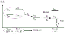

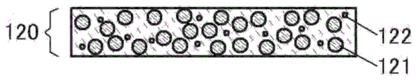


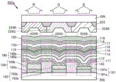


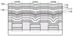

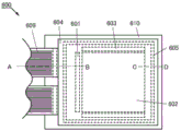
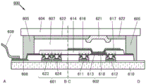


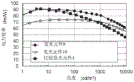


Classifications
-
- C—CHEMISTRY; METALLURGY
- C07—ORGANIC CHEMISTRY
- C07F—ACYCLIC, CARBOCYCLIC OR HETEROCYCLIC COMPOUNDS CONTAINING ELEMENTS OTHER THAN CARBON, HYDROGEN, HALOGEN, OXYGEN, NITROGEN, SULFUR, SELENIUM OR TELLURIUM
- C07F15/00—Compounds containing elements of Groups 8, 9, 10 or 18 of the Periodic System
- C07F15/0006—Compounds containing elements of Groups 8, 9, 10 or 18 of the Periodic System compounds of the platinum group
- C07F15/0033—Iridium compounds
-
- C—CHEMISTRY; METALLURGY
- C09—DYES; PAINTS; POLISHES; NATURAL RESINS; ADHESIVES; COMPOSITIONS NOT OTHERWISE PROVIDED FOR; APPLICATIONS OF MATERIALS NOT OTHERWISE PROVIDED FOR
- C09K—MATERIALS FOR MISCELLANEOUS APPLICATIONS, NOT PROVIDED FOR ELSEWHERE
- C09K11/00—Luminescent, e.g. electroluminescent, chemiluminescent materials
- C09K11/06—Luminescent, e.g. electroluminescent, chemiluminescent materials containing organic luminescent materials
-
- H—ELECTRICITY
- H10—SEMICONDUCTOR DEVICES; ELECTRIC SOLID-STATE DEVICES NOT OTHERWISE PROVIDED FOR
- H10K—ORGANIC ELECTRIC SOLID-STATE DEVICES
- H10K50/00—Organic light-emitting devices
- H10K50/10—OLEDs or polymer light-emitting diodes [PLED]
- H10K50/11—OLEDs or polymer light-emitting diodes [PLED] characterised by the electroluminescent [EL] layers
- H10K50/12—OLEDs or polymer light-emitting diodes [PLED] characterised by the electroluminescent [EL] layers comprising dopants
- H10K50/121—OLEDs or polymer light-emitting diodes [PLED] characterised by the electroluminescent [EL] layers comprising dopants for assisting energy transfer, e.g. sensitization
-
- H—ELECTRICITY
- H10—SEMICONDUCTOR DEVICES; ELECTRIC SOLID-STATE DEVICES NOT OTHERWISE PROVIDED FOR
- H10K—ORGANIC ELECTRIC SOLID-STATE DEVICES
- H10K50/00—Organic light-emitting devices
- H10K50/10—OLEDs or polymer light-emitting diodes [PLED]
- H10K50/14—Carrier transporting layers
- H10K50/15—Hole transporting layers
-
- H—ELECTRICITY
- H10—SEMICONDUCTOR DEVICES; ELECTRIC SOLID-STATE DEVICES NOT OTHERWISE PROVIDED FOR
- H10K—ORGANIC ELECTRIC SOLID-STATE DEVICES
- H10K50/00—Organic light-emitting devices
- H10K50/10—OLEDs or polymer light-emitting diodes [PLED]
- H10K50/14—Carrier transporting layers
- H10K50/16—Electron transporting layers
-
- H—ELECTRICITY
- H10—SEMICONDUCTOR DEVICES; ELECTRIC SOLID-STATE DEVICES NOT OTHERWISE PROVIDED FOR
- H10K—ORGANIC ELECTRIC SOLID-STATE DEVICES
- H10K50/00—Organic light-emitting devices
- H10K50/80—Constructional details
- H10K50/84—Passivation; Containers; Encapsulations
-
- H—ELECTRICITY
- H10—SEMICONDUCTOR DEVICES; ELECTRIC SOLID-STATE DEVICES NOT OTHERWISE PROVIDED FOR
- H10K—ORGANIC ELECTRIC SOLID-STATE DEVICES
- H10K59/00—Integrated devices, or assemblies of multiple devices, comprising at least one organic light-emitting element covered by group H10K50/00
- H10K59/10—OLED displays
- H10K59/12—Active-matrix OLED [AMOLED] displays
- H10K59/121—Active-matrix OLED [AMOLED] displays characterised by the geometry or disposition of pixel elements
- H10K59/1213—Active-matrix OLED [AMOLED] displays characterised by the geometry or disposition of pixel elements the pixel elements being TFTs
-
- H—ELECTRICITY
- H10—SEMICONDUCTOR DEVICES; ELECTRIC SOLID-STATE DEVICES NOT OTHERWISE PROVIDED FOR
- H10K—ORGANIC ELECTRIC SOLID-STATE DEVICES
- H10K59/00—Integrated devices, or assemblies of multiple devices, comprising at least one organic light-emitting element covered by group H10K50/00
- H10K59/30—Devices specially adapted for multicolour light emission
- H10K59/38—Devices specially adapted for multicolour light emission comprising colour filters or colour changing media [CCM]
-
- H—ELECTRICITY
- H10—SEMICONDUCTOR DEVICES; ELECTRIC SOLID-STATE DEVICES NOT OTHERWISE PROVIDED FOR
- H10K—ORGANIC ELECTRIC SOLID-STATE DEVICES
- H10K59/00—Integrated devices, or assemblies of multiple devices, comprising at least one organic light-emitting element covered by group H10K50/00
- H10K59/40—OLEDs integrated with touch screens
-
- H—ELECTRICITY
- H10—SEMICONDUCTOR DEVICES; ELECTRIC SOLID-STATE DEVICES NOT OTHERWISE PROVIDED FOR
- H10K—ORGANIC ELECTRIC SOLID-STATE DEVICES
- H10K59/00—Integrated devices, or assemblies of multiple devices, comprising at least one organic light-emitting element covered by group H10K50/00
- H10K59/80—Constructional details
- H10K59/87—Passivation; Containers; Encapsulations
-
- C—CHEMISTRY; METALLURGY
- C09—DYES; PAINTS; POLISHES; NATURAL RESINS; ADHESIVES; COMPOSITIONS NOT OTHERWISE PROVIDED FOR; APPLICATIONS OF MATERIALS NOT OTHERWISE PROVIDED FOR
- C09K—MATERIALS FOR MISCELLANEOUS APPLICATIONS, NOT PROVIDED FOR ELSEWHERE
- C09K2211/00—Chemical nature of organic luminescent or tenebrescent compounds
- C09K2211/10—Non-macromolecular compounds
- C09K2211/1003—Carbocyclic compounds
- C09K2211/1007—Non-condensed systems
-
- C—CHEMISTRY; METALLURGY
- C09—DYES; PAINTS; POLISHES; NATURAL RESINS; ADHESIVES; COMPOSITIONS NOT OTHERWISE PROVIDED FOR; APPLICATIONS OF MATERIALS NOT OTHERWISE PROVIDED FOR
- C09K—MATERIALS FOR MISCELLANEOUS APPLICATIONS, NOT PROVIDED FOR ELSEWHERE
- C09K2211/00—Chemical nature of organic luminescent or tenebrescent compounds
- C09K2211/10—Non-macromolecular compounds
- C09K2211/1003—Carbocyclic compounds
- C09K2211/1011—Condensed systems
-
- C—CHEMISTRY; METALLURGY
- C09—DYES; PAINTS; POLISHES; NATURAL RESINS; ADHESIVES; COMPOSITIONS NOT OTHERWISE PROVIDED FOR; APPLICATIONS OF MATERIALS NOT OTHERWISE PROVIDED FOR
- C09K—MATERIALS FOR MISCELLANEOUS APPLICATIONS, NOT PROVIDED FOR ELSEWHERE
- C09K2211/00—Chemical nature of organic luminescent or tenebrescent compounds
- C09K2211/10—Non-macromolecular compounds
- C09K2211/1018—Heterocyclic compounds
- C09K2211/1025—Heterocyclic compounds characterised by ligands
- C09K2211/1059—Heterocyclic compounds characterised by ligands containing three nitrogen atoms as heteroatoms
-
- C—CHEMISTRY; METALLURGY
- C09—DYES; PAINTS; POLISHES; NATURAL RESINS; ADHESIVES; COMPOSITIONS NOT OTHERWISE PROVIDED FOR; APPLICATIONS OF MATERIALS NOT OTHERWISE PROVIDED FOR
- C09K—MATERIALS FOR MISCELLANEOUS APPLICATIONS, NOT PROVIDED FOR ELSEWHERE
- C09K2211/00—Chemical nature of organic luminescent or tenebrescent compounds
- C09K2211/18—Metal complexes
- C09K2211/185—Metal complexes of the platinum group, i.e. Os, Ir, Pt, Ru, Rh or Pd
-
- H—ELECTRICITY
- H10—SEMICONDUCTOR DEVICES; ELECTRIC SOLID-STATE DEVICES NOT OTHERWISE PROVIDED FOR
- H10K—ORGANIC ELECTRIC SOLID-STATE DEVICES
- H10K2101/00—Properties of the organic materials covered by group H10K85/00
- H10K2101/10—Triplet emission
-
- H—ELECTRICITY
- H10—SEMICONDUCTOR DEVICES; ELECTRIC SOLID-STATE DEVICES NOT OTHERWISE PROVIDED FOR
- H10K—ORGANIC ELECTRIC SOLID-STATE DEVICES
- H10K2101/00—Properties of the organic materials covered by group H10K85/00
- H10K2101/20—Delayed fluorescence emission
- H10K2101/25—Delayed fluorescence emission using exciplex
-
- H—ELECTRICITY
- H10—SEMICONDUCTOR DEVICES; ELECTRIC SOLID-STATE DEVICES NOT OTHERWISE PROVIDED FOR
- H10K—ORGANIC ELECTRIC SOLID-STATE DEVICES
- H10K2101/00—Properties of the organic materials covered by group H10K85/00
- H10K2101/30—Highest occupied molecular orbital [HOMO], lowest unoccupied molecular orbital [LUMO] or Fermi energy values
-
- H—ELECTRICITY
- H10—SEMICONDUCTOR DEVICES; ELECTRIC SOLID-STATE DEVICES NOT OTHERWISE PROVIDED FOR
- H10K—ORGANIC ELECTRIC SOLID-STATE DEVICES
- H10K2101/00—Properties of the organic materials covered by group H10K85/00
- H10K2101/40—Interrelation of parameters between multiple constituent active layers or sublayers, e.g. HOMO values in adjacent layers
-
- H—ELECTRICITY
- H10—SEMICONDUCTOR DEVICES; ELECTRIC SOLID-STATE DEVICES NOT OTHERWISE PROVIDED FOR
- H10K—ORGANIC ELECTRIC SOLID-STATE DEVICES
- H10K2101/00—Properties of the organic materials covered by group H10K85/00
- H10K2101/80—Composition varying spatially, e.g. having a spatial gradient
-
- H—ELECTRICITY
- H10—SEMICONDUCTOR DEVICES; ELECTRIC SOLID-STATE DEVICES NOT OTHERWISE PROVIDED FOR
- H10K—ORGANIC ELECTRIC SOLID-STATE DEVICES
- H10K2101/00—Properties of the organic materials covered by group H10K85/00
- H10K2101/90—Multiple hosts in the emissive layer
-
- H—ELECTRICITY
- H10—SEMICONDUCTOR DEVICES; ELECTRIC SOLID-STATE DEVICES NOT OTHERWISE PROVIDED FOR
- H10K—ORGANIC ELECTRIC SOLID-STATE DEVICES
- H10K85/00—Organic materials used in the body or electrodes of devices covered by this subclass
- H10K85/30—Coordination compounds
- H10K85/341—Transition metal complexes, e.g. Ru(II)polypyridine complexes
- H10K85/342—Transition metal complexes, e.g. Ru(II)polypyridine complexes comprising iridium
-
- H—ELECTRICITY
- H10—SEMICONDUCTOR DEVICES; ELECTRIC SOLID-STATE DEVICES NOT OTHERWISE PROVIDED FOR
- H10K—ORGANIC ELECTRIC SOLID-STATE DEVICES
- H10K85/00—Organic materials used in the body or electrodes of devices covered by this subclass
- H10K85/60—Organic compounds having low molecular weight
- H10K85/615—Polycyclic condensed aromatic hydrocarbons, e.g. anthracene
-
- H—ELECTRICITY
- H10—SEMICONDUCTOR DEVICES; ELECTRIC SOLID-STATE DEVICES NOT OTHERWISE PROVIDED FOR
- H10K—ORGANIC ELECTRIC SOLID-STATE DEVICES
- H10K85/00—Organic materials used in the body or electrodes of devices covered by this subclass
- H10K85/60—Organic compounds having low molecular weight
- H10K85/631—Amine compounds having at least two aryl rest on at least one amine-nitrogen atom, e.g. triphenylamine
- H10K85/633—Amine compounds having at least two aryl rest on at least one amine-nitrogen atom, e.g. triphenylamine comprising polycyclic condensed aromatic hydrocarbons as substituents on the nitrogen atom
-
- H—ELECTRICITY
- H10—SEMICONDUCTOR DEVICES; ELECTRIC SOLID-STATE DEVICES NOT OTHERWISE PROVIDED FOR
- H10K—ORGANIC ELECTRIC SOLID-STATE DEVICES
- H10K85/00—Organic materials used in the body or electrodes of devices covered by this subclass
- H10K85/60—Organic compounds having low molecular weight
- H10K85/631—Amine compounds having at least two aryl rest on at least one amine-nitrogen atom, e.g. triphenylamine
- H10K85/636—Amine compounds having at least two aryl rest on at least one amine-nitrogen atom, e.g. triphenylamine comprising heteroaromatic hydrocarbons as substituents on the nitrogen atom
-
- H—ELECTRICITY
- H10—SEMICONDUCTOR DEVICES; ELECTRIC SOLID-STATE DEVICES NOT OTHERWISE PROVIDED FOR
- H10K—ORGANIC ELECTRIC SOLID-STATE DEVICES
- H10K85/00—Organic materials used in the body or electrodes of devices covered by this subclass
- H10K85/60—Organic compounds having low molecular weight
- H10K85/649—Aromatic compounds comprising a hetero atom
- H10K85/654—Aromatic compounds comprising a hetero atom comprising only nitrogen as heteroatom
-
- H—ELECTRICITY
- H10—SEMICONDUCTOR DEVICES; ELECTRIC SOLID-STATE DEVICES NOT OTHERWISE PROVIDED FOR
- H10K—ORGANIC ELECTRIC SOLID-STATE DEVICES
- H10K85/00—Organic materials used in the body or electrodes of devices covered by this subclass
- H10K85/60—Organic compounds having low molecular weight
- H10K85/649—Aromatic compounds comprising a hetero atom
- H10K85/657—Polycyclic condensed heteroaromatic hydrocarbons
- H10K85/6572—Polycyclic condensed heteroaromatic hydrocarbons comprising only nitrogen in the heteroaromatic polycondensed ring system, e.g. phenanthroline or carbazole
-
- H—ELECTRICITY
- H10—SEMICONDUCTOR DEVICES; ELECTRIC SOLID-STATE DEVICES NOT OTHERWISE PROVIDED FOR
- H10K—ORGANIC ELECTRIC SOLID-STATE DEVICES
- H10K85/00—Organic materials used in the body or electrodes of devices covered by this subclass
- H10K85/60—Organic compounds having low molecular weight
- H10K85/649—Aromatic compounds comprising a hetero atom
- H10K85/657—Polycyclic condensed heteroaromatic hydrocarbons
- H10K85/6576—Polycyclic condensed heteroaromatic hydrocarbons comprising only sulfur in the heteroaromatic polycondensed ring system, e.g. benzothiophene
Abstract
The invention provides a light-emitting element with high light-emitting efficiency. The light-emitting element includes a first organic compound having an electron-transporting property, a second organic compound having a hole-transporting property, and a guest material. The first organic compound forms an exciplex with the second organic compound. The guest material converts triplet excitation energy into luminescence. The energy difference between the lowest unoccupied molecular orbital energy level of the first organic compound and the highest occupied molecular orbital energy level of the guest material is equal to or greater than the light emission energy of the guest material.
Description
The present application is a divisional application of a chinese patent application titled "light emitting element, display device, electronic device, and lighting device" of national application No. 201680042978.1 after PCT international application No. PCT/IB2016/054163, international application No. 2016, 7, 13 enters the chinese stage.
Technical Field
One embodiment of the present invention relates to a light-emitting element, a display device including the light-emitting element, an electronic device, and a lighting device.
Note that one embodiment of the present invention is not limited to the above-described technical field. The technical field of one embodiment of the invention disclosed in the present specification and the like relates to an object, a method, or a manufacturing method. In addition, one embodiment of the present invention relates to a process, a machine, a product, or a composition (composition of matter). Specifically, examples of the technical field of one embodiment of the present invention disclosed in the present specification include semiconductor devices, display devices, liquid crystal display devices, light-emitting devices, lighting devices, power storage devices, driving methods of these devices, and manufacturing methods of these devices.
Background
In recent years, research and development of light emitting elements using Electroluminescence (EL) have been increasingly performed. In the basic structure of these light-emitting elements, a layer (EL layer) containing a light-emitting material is sandwiched between a pair of electrodes. By applying a voltage between a pair of electrodes of the element, light emission from the light emitting material can be obtained.
Since the light-emitting element is a self-luminous light-emitting element, a display device using the light-emitting element has the following advantages: good visibility; no backlight is required; and low power consumption. And, this display device still has following advantage: can be made thin and light; high response speed.
In a light-emitting element (for example, an organic EL element) in which an organic material is used as a light-emitting material and an EL layer containing the light-emitting material is provided between a pair of electrodes, electrons and holes are injected from a cathode and an anode, respectively, to the EL layer having a light-emitting function by applying a voltage between the pair of electrodes, whereby a current flows. The injected electrons and holes are recombined to bring the organic material having a light emitting function into an excited state, and light emission can be obtained.
The excited state formed by the organic material may be a singlet excited state (S * ) Or triplet excited state (T) * ). Luminescence from singlet excited statesReferred to as fluorescence, and luminescence from a triplet excited state is referred to as phosphorescence. In the light-emitting element, S * And T is * The production ratio of (2) is 1:3. in other words, the light-emitting element including a material that emits phosphorescence (phosphorescent material) has higher light-emitting efficiency than the light-emitting element including a material that emits fluorescence (fluorescent material). Accordingly, in recent years, a light-emitting element using a phosphorescent material capable of converting a triplet excited state into luminescence has been actively developed (for example, refer to patent document 1).
The energy required for excitation of an organic material depends on the energy difference between the LUMO (lowest unoccupied molecular orbital) energy level and the HOMO (highest occupied molecular orbital) energy level of the organic material. This energy difference corresponds approximately to the energy of the singlet excited state. In a light-emitting element including an organic material that emits phosphorescence, triplet excitation energy is converted into energy of light emission. Thus, when the energy difference between the singlet excited state and the triplet excited state of the organic material is large, the energy used to excite the organic material is higher than the energy used to emit light, and the difference therebetween corresponds to the energy difference. The energy difference between the energy used to excite the organic material and the energy of light emission affects the element characteristics of the light emitting element: the driving voltage of the light emitting element is increased. A method of suppressing the rise in the driving voltage is being studied and developed (see patent document 2).
In a light-emitting element including a phosphorescent material, particularly, a light-emitting element exhibiting blue light emission, development of a stable compound having a high triplet excitation level is difficult, and thus, practical use has not been achieved. Therefore, development of a phosphorescent material having high light emission efficiency and stability and a phosphorescent light emitting element exhibiting high light emission efficiency and excellent reliability are demanded.
[ reference ]
[ patent literature ]
[ patent document 2] Japanese patent application laid-open No. 2012-212879
Disclosure of Invention
Iridium complexes are known as phosphorescent materials exhibiting high luminous efficiency. As iridium complexes having high luminous energy, iridium complexes having a pyridine skeleton or a nitrogen-containing five-membered heterocyclic skeleton in the ligand are known. Although the pyridine skeleton or the nitrogen-containing five-membered heterocyclic skeleton has high triplet excitation energy, its electron-receiving property is low. Therefore, the iridium complex having the above skeleton in the ligand has a high HOMO level and LUMO level, and hole carriers are easily injected, and electron carriers are not easily injected. As a result, when an iridium complex having high light-emission energy is used, it may be difficult to form an excited state by direct recombination of carriers or to cause a light-emitting element to emit light with high efficiency.
In view of the above, an object of one embodiment of the present invention is to provide a light-emitting element which includes a phosphorescent material and has high light-emitting efficiency. Another object of one embodiment of the present invention is to provide a light-emitting element with reduced power consumption. Another object of one embodiment of the present invention is to provide a light-emitting element with high reliability. It is another object of one embodiment of the present invention to provide a novel light-emitting element. It is another object of one embodiment of the present invention to provide a novel light emitting device. It is another object of one embodiment of the present invention to provide a novel display device.
Note that the description of the above objects does not hinder the existence of other objects. In one embodiment of the present invention, it is not necessary to achieve all of the above objects. Other objects than the above objects can be obtained and extracted from the description of the specification and the like.
One embodiment of the present invention is a light-emitting element including an exciplex capable of exciting a phosphorescent material with high efficiency.
Thus, one embodiment of the present invention is a light-emitting element including: a first organic compound; a second organic compound; a guest material. The LUMO energy level of the first organic compound is lower than the LUMO energy level of the second organic compound. The HOMO level of the first organic compound is lower than the HOMO level of the second organic compound. The guest material has a HOMO level higher than that of the second organic compound. The energy difference between the LUMO energy level of the guest material and the HOMO energy level of the guest material is greater than the energy difference between the LUMO energy level of the first organic compound and the HOMO energy level of the second organic compound. The guest material has a function of converting triplet excitation energy into luminescence. The combination of the first organic compound and the second organic compound forms an exciplex.
In the above structure, it is preferable that the energy difference between the LUMO level of the first organic compound and the HOMO level of the second organic compound is equal to or greater than the migration energy calculated from the absorption edge of the absorption spectrum of the guest material. Preferably, the energy difference between the LUMO level of the first organic compound and the HOMO level of the second organic compound is greater than or equal to the energy of luminescence exhibited by the guest material.
Another embodiment of the present invention is a light-emitting element including: a first organic compound; a second organic compound; a guest material. The LUMO energy level of the first organic compound is lower than the LUMO energy level of the second organic compound. The HOMO level of the first organic compound is lower than the HOMO level of the second organic compound. The guest material has a HOMO level higher than that of the second organic compound. The energy difference between the LUMO energy level of the guest material and the HOMO energy level of the guest material is greater than the energy difference between the LUMO energy level of the first organic compound and the HOMO energy level of the second organic compound. The guest material has a function of converting triplet excitation energy into luminescence. The combination of the first organic compound and the second organic compound forms an exciplex. The energy difference between the LUMO level of the first organic compound and the HOMO level of the guest material is equal to or greater than the migration energy calculated from the absorption edge of the absorption spectrum of the guest material.
Another embodiment of the present invention is a light-emitting element including: a first organic compound; a second organic compound; a guest material. The LUMO energy level of the first organic compound is lower than the LUMO energy level of the second organic compound. The HOMO level of the first organic compound is lower than the HOMO level of the second organic compound. The guest material has a HOMO level higher than that of the second organic compound. The energy difference between the LUMO energy level of the guest material and the HOMO energy level of the guest material is greater than the energy difference between the LUMO energy level of the first organic compound and the HOMO energy level of the second organic compound. The guest material has a function of converting triplet excitation energy into luminescence. The combination of the first organic compound and the second organic compound forms an exciplex. The energy difference between the LUMO level of the first organic compound and the HOMO level of the guest material is equal to or greater than the energy of luminescence exhibited by the guest material.
In each of the above structures, it is preferable that the energy difference between the LUMO level of the guest material and the HOMO level of the guest material is 0.3eV or more larger than the migration energy calculated from the absorption edge of the absorption spectrum of the guest material.
In each of the above structures, it is preferable that the energy difference between the LUMO level of the guest material and the HOMO level of the guest material is 0.3eV or more larger than the energy of light emission exhibited by the guest material.
In each of the above structures, it is preferable that the exciplex has a function of supplying excitation energy to the guest material. Further, it is preferable that the exciplex exhibits an emission spectrum having a region overlapping with an absorption band on the longest wavelength side in the absorption spectrum of the guest material.
In each of the above structures, the guest material preferably contains iridium.
In each of the above structures, it is preferable that the guest material contains a ligand which is coordinated to iridium, and the ligand has a cyano group and a nitrogen-containing five-membered heterocyclic skeleton. Preferably, the ligand has a cyano group and a triazole skeleton.
In each of the above structures, the first organic compound preferably has a function of transporting electrons, and the second organic compound preferably has a function of transporting holes. The first organic compound preferably has a pi-electron-deficient aromatic heterocyclic skeleton, and the second organic compound preferably has at least one of a pi-electron-rich aromatic heterocyclic skeleton and an aromatic amine skeleton.
Another aspect of the present invention is a display device including: a light-emitting element having any one of the above structures; and at least one of a color filter and a transistor. Another aspect of the present invention is an electronic apparatus including: the display device; and at least one of a frame and a touch sensor. Another aspect of the present invention is a lighting device including: a light-emitting element having any one of the above structures; and at least one of a frame and a touch sensor. One embodiment of the present invention includes not only a light-emitting device including a light-emitting element but also an electronic device including a light-emitting device. The light emitting device in this specification refers to an image display device and a light source (e.g., a lighting device). The following display module is also one mode of the present invention: a display module in which a connector such as FPC (flexible printed circuit: flexible circuit board) or TCP (tape carrier package: tape carrier package) is mounted in the light emitting device; a display module of a printed circuit board is arranged at the end part of the TCP; and a display module in which an IC (integrated circuit) is directly mounted on the light emitting element by a Chip On Glass (COG) method.
According to one embodiment of the present invention, a light-emitting element including a phosphorescent material and having high light-emitting efficiency can be provided. According to one embodiment of the present invention, a light-emitting element with reduced power consumption can be provided. According to one embodiment of the present invention, a light-emitting element with high reliability can be provided. According to one embodiment of the present invention, a novel light-emitting element can be provided. According to one embodiment of the present invention, a novel light emitting device can be provided. According to one embodiment of the present invention, a novel display device can be provided.
Note that the description of these effects does not hinder the existence of other effects. One embodiment of the present invention does not necessarily require all of the above effects to be achieved. Further, it is apparent that effects other than the above-described effects exist in the descriptions of the specification, drawings, claims, and the like, and effects other than the above-described effects can be obtained from the descriptions of the specification, drawings, claims, and the like.
Drawings
Fig. 1A and 1B are schematic cross-sectional views of a light-emitting element according to an embodiment of the present invention;
fig. 2A and 2B illustrate a correlation of energy bands and a correlation of energy levels in a light-emitting layer of a light-emitting element according to an embodiment of the present invention;
Fig. 3A to 3C are schematic cross-sectional views of a light-emitting element according to an embodiment of the present invention and diagrams illustrating a correlation of energy levels;
fig. 4A to 4C are schematic cross-sectional views of a light-emitting element according to an embodiment of the present invention and diagrams illustrating a correlation of energy levels;
fig. 5A and 5B are schematic cross-sectional views of a light-emitting element according to an embodiment of the present invention;
fig. 6A and 6B are schematic cross-sectional views of a light-emitting element according to an embodiment of the present invention;
fig. 7A to 7C are schematic cross-sectional views illustrating a method of manufacturing a light-emitting element according to an embodiment of the present invention;
fig. 8A to 8C are schematic cross-sectional views illustrating a method of manufacturing a light-emitting element according to an embodiment of the present invention;
fig. 9A and 9B are a plan view and a schematic sectional view of a display device according to an embodiment of the present invention;
fig. 10A and 10B are schematic cross-sectional views illustrating a display device according to an embodiment of the present invention;
fig. 11 is a schematic cross-sectional view of a display device illustrating an embodiment of the present invention;
fig. 12A and 12B are schematic cross-sectional views of a display device illustrating an embodiment of the present invention;
fig. 13A and 13B are schematic cross-sectional views of a display device illustrating an embodiment of the present invention;
fig. 14 is a schematic cross-sectional view of a display device illustrating an embodiment of the present invention;
Fig. 15A and 15B are schematic cross-sectional views of a display device illustrating an embodiment of the present invention;
fig. 16 is a schematic cross-sectional view of a display device illustrating an embodiment of the present invention;
fig. 17A and 17B are schematic cross-sectional views of a display device illustrating an embodiment of the present invention;
fig. 18A and 18B are a block diagram and a circuit diagram of a display device according to an embodiment of the present invention;
fig. 19A and 19B are circuit diagrams illustrating pixel circuits of a display device according to an embodiment of the present invention;
fig. 20A and 20B are circuit diagrams illustrating pixel circuits of a display device according to an embodiment of the present invention;
fig. 21A and 21B are perspective views showing an example of a touch panel according to an embodiment of the present invention;
fig. 22A to 22C are cross-sectional views showing an example of a display device and a touch sensor according to an embodiment of the present invention;
fig. 23A and 23B are cross-sectional views showing an example of a touch panel according to an embodiment of the present invention;
FIGS. 24A and 24B are block and timing diagrams of a touch sensor in accordance with one embodiment of the invention;
FIG. 25 is a circuit diagram of a touch sensor in accordance with one embodiment of the invention;
fig. 26 is a perspective view illustrating a display module according to an embodiment of the present invention;
Fig. 27A to 27G illustrate an electronic device of an embodiment of the present invention;
fig. 28A to 28D illustrate an electronic device according to an embodiment of the present invention;
fig. 29A and 29B are perspective views illustrating a display device according to an embodiment of the present invention;
fig. 30A to 30C are perspective views and cross-sectional views illustrating a light emitting device according to an embodiment of the present invention;
fig. 31A to 31D are sectional views illustrating a light emitting device according to an embodiment of the present invention;
fig. 32A and 32B illustrate an electronic device according to an embodiment of the present invention, and fig. 32C illustrates a lighting device according to an embodiment of the present invention;
FIG. 33 illustrates an illumination device according to an embodiment of the present invention;
fig. 34 is a schematic sectional view illustrating a light emitting element in the embodiment;
FIG. 35 is a diagram illustrating an emission spectrum of a host material in the embodiment;
fig. 36A and 36B are diagrams illustrating absorption spectra and emission spectra of guest materials in the embodiment;
FIG. 37 is a diagram illustrating phosphorescence emission spectra of a host material in an embodiment;
fig. 38 is a diagram illustrating current efficiency-luminance characteristics of the light emitting element in the embodiment;
fig. 39 is a diagram illustrating luminance-voltage characteristics of the light emitting element in the embodiment;
fig. 40 is a diagram illustrating external quantum efficiency-luminance characteristics of the light emitting element in the embodiment;
Fig. 41 is a diagram illustrating power efficiency-luminance characteristics of the light emitting element in the embodiment;
fig. 42 is a diagram illustrating an electroluminescence emission spectrum of the light emitting element in the embodiment;
fig. 43 is a diagram illustrating a reliability test result of the light emitting element in the embodiment;
FIG. 44 is a diagram illustrating an emission spectrum of a host material in the embodiment;
fig. 45A and 45B are diagrams illustrating absorption spectra and emission spectra of guest materials in the embodiment;
fig. 46 is a diagram illustrating current efficiency-luminance characteristics of the light emitting element in the embodiment;
fig. 47 is a diagram illustrating luminance-voltage characteristics of the light emitting element in the embodiment;
fig. 48 is a diagram illustrating external quantum efficiency-luminance characteristics of the light emitting element in the embodiment;
fig. 49 is a diagram illustrating power efficiency-luminance characteristics of the light emitting element in the embodiment;
fig. 50 is a diagram illustrating an electroluminescence emission spectrum of a light emitting element in the embodiment;
fig. 51A and 51B are diagrams illustrating the correlation of energy bands in the embodiment;
fig. 52 is a diagram illustrating the reliability test result of the light emitting element in the embodiment;
fig. 53 is a graph illustrating an absorption spectrum and an emission spectrum of the guest material in the embodiment;
fig. 54 is a graph illustrating an absorption spectrum and an emission spectrum of the guest material in the embodiment;
Fig. 55 is a graph illustrating an absorption spectrum and an emission spectrum of the guest material in the example;
fig. 56 is a diagram illustrating current efficiency-luminance characteristics of the light emitting element in the embodiment;
fig. 57 is a diagram illustrating luminance-voltage characteristics of the light emitting element in the embodiment;
fig. 58 is a diagram illustrating external quantum efficiency-luminance characteristics of the light emitting element in the embodiment;
fig. 59 is a diagram illustrating power efficiency-luminance characteristics of the light emitting element in the embodiment;
fig. 60 is a diagram illustrating an electroluminescence emission spectrum of the light emitting element in the embodiment;
FIG. 61 is a diagram illustrating an emission spectrum of a host material in an embodiment;
fig. 62 is a graph illustrating an absorption spectrum of the guest material in the embodiment;
FIG. 63 is a diagram illustrating the phosphorescence emission spectrum of a host material in an embodiment;
fig. 64 is a diagram illustrating current efficiency-luminance characteristics of the light emitting element in the embodiment;
fig. 65 is a diagram illustrating luminance-voltage characteristics of the light emitting element in the embodiment;
fig. 66 is a diagram illustrating external quantum efficiency-luminance characteristics of the light emitting element in the embodiment;
fig. 67 is a diagram illustrating power efficiency-luminance characteristics of the light emitting element in the embodiment;
fig. 68 is a diagram illustrating an electroluminescence emission spectrum of the light emitting element in the embodiment;
Fig. 69 is a graph illustrating an absorption spectrum and an emission spectrum of the guest material in the embodiment;
fig. 70 is a diagram illustrating current efficiency-luminance characteristics of the light emitting element in the embodiment;
fig. 71 is a diagram illustrating luminance-voltage characteristics of the light emitting element in the embodiment;
fig. 72 is a diagram illustrating external quantum efficiency-luminance characteristics of the light emitting element in the embodiment;
fig. 73 is a diagram illustrating power efficiency-luminance characteristics of the light emitting element in the embodiment;
fig. 74 is a diagram illustrating an electroluminescence emission spectrum of the light emitting element in the embodiment;
fig. 75 is a diagram illustrating current efficiency-luminance characteristics of the light emitting element in the embodiment;
fig. 76 is a diagram illustrating luminance-voltage characteristics of the light emitting element in the embodiment;
fig. 77 is a diagram illustrating external quantum efficiency-luminance characteristics of a light emitting element in the embodiment;
fig. 78 is a diagram illustrating power efficiency-luminance characteristics of the light emitting element in the embodiment;
fig. 79 is a diagram illustrating an electroluminescence emission spectrum of the light emitting element in the embodiment;
FIG. 80 is a diagram illustrating an emission spectrum of a host material in an embodiment;
fig. 81 is a diagram illustrating current efficiency-luminance characteristics of the light emitting element in the embodiment;
fig. 82 is a diagram illustrating luminance-voltage characteristics of the light emitting element in the embodiment;
Fig. 83 is a diagram illustrating external quantum efficiency-luminance characteristics of the light emitting element in the embodiment;
fig. 84 is a diagram illustrating an electroluminescence emission spectrum of the light emitting element in the embodiment;
fig. 85 is a graph illustrating an absorption spectrum and an emission spectrum of the guest material in the embodiment;
FIG. 86 is a diagram illustrating phosphorescence emission spectra of a host material in an embodiment;
fig. 87 is a diagram illustrating the reliability test result of the light emitting element in the embodiment;
fig. 88 is a diagram illustrating current efficiency-luminance characteristics of the light emitting element in the embodiment;
fig. 89 is a diagram illustrating luminance-voltage characteristics of the light emitting element in the embodiment;
fig. 90 is a diagram illustrating external quantum efficiency-luminance characteristics of the light emitting element in the embodiment;
fig. 91 is a diagram illustrating current efficiency-luminance characteristics of the light emitting element in the embodiment;
fig. 92 is a diagram illustrating an electroluminescence emission spectrum of the light emitting element in the embodiment;
fig. 93 is a diagram illustrating phosphorescence emission spectra of a host material in an embodiment.
Detailed Description
Hereinafter, embodiments of the present invention will be described in detail with reference to the accompanying drawings. Note that the present invention is not limited to the following description, and its modes and details can be changed into various forms without departing from the spirit and scope of the present invention. Therefore, the present invention should not be construed as being limited to the description of the embodiments shown below.
For ease of understanding, the positions, sizes, ranges, and the like of the respective structures shown in the drawings and the like may not indicate actual positions, sizes, ranges, and the like. Accordingly, the disclosed invention is not necessarily limited to the disclosed positions, sizes, ranges, etc. of the drawings, etc.
In this specification and the like, ordinal numbers such as "first" and "second" are appended for convenience, and may not indicate the process order or the lamination order. Therefore, for example, the description may be given by appropriately replacing "first" with "second" or "third" or the like. Further, the ordinal words described in the specification and the like may not coincide with ordinal words for specifying one embodiment of the present invention.
In the present specification and the like, when the structure of the invention is described using the drawings, the same reference numerals are used in common in different drawings.
In this specification and the like, "film" and "layer" may be exchanged with each other. For example, the "conductive layer" may be sometimes referred to as "conductive film". In addition, the "insulating film" may be sometimes referred to as an "insulating layer".
In the present specification and the like, the singlet excited state (S * ) Refers to a singlet state having excitation energy. The S1 level is the lowest level of the singlet excited states, which refers to the excitation level of the lowest singlet excited state. Triplet excited state (T) * ) Refers to a triplet state having excitation energy. The T1 level is the lowest level of the triplet excited states, which refers to the excited level of the lowest triplet excited state. In the present specification and the like, a singlet excited state and a singlet excited state energy level may be respectively differentRepresenting the lowest singlet excited state and S1 energy level. The triplet excited state and the triplet excited state energy level sometimes represent the lowest triplet excited state and T1 energy level, respectively.
In this specification and the like, the fluorescent material means a material that emits light in the visible light region when returning from a singlet excited state to a ground state. The phosphorescent material refers to a material that emits light in the visible light region at room temperature upon returning from a triplet excited state to a ground state. In other words, the phosphorescent material refers to a material capable of converting triplet excitation energy into visible light.
Phosphorescent light emission energy or triplet excitation state energy can be derived from the wavelength of the emission peak (including the shoulder peak) on the shortest wavelength side of phosphorescent light emission. In addition, the above-described phosphorescent emission can be observed by time-resolved photoluminescence spectrum under a low temperature (e.g., 10K) environment. The emission energy of the thermally-activated delayed fluorescence can be derived from the wavelength of the emission peak (including the shoulder) on the shortest wavelength side of the thermally-activated delayed fluorescence.
In the present specification and the like, the term "room temperature" means a temperature of 0 ℃ or higher and 40 ℃ or lower.
In the present specification, the blue wavelength region refers to a wavelength region of 400nm or more and less than 505nm, and blue light emission has at least one emission spectrum peak in the wavelength region. The green wavelength region is a wavelength region of 505nm or more and less than 580nm, and the green light emission has at least one emission spectrum peak in the wavelength region. The red wavelength region is a wavelength region of 580nm or more and 680nm or less, and the red luminescence has at least one emission spectrum peak in the wavelength region.
In this embodiment mode, a light-emitting element according to an embodiment of the present invention is described with reference to fig. 1A and 1B and fig. 2A and 2B.
< structural example of light-emitting element >
First, a structure of a light-emitting element according to one embodiment of the present invention will be described with reference to fig. 1A and 1B.
Fig. 1A is a schematic cross-sectional view of a light-emitting element 150 according to an embodiment of the present invention.
The light-emitting element 150 includes a pair of electrodes (an electrode 101 and an electrode 102) and an EL layer 100 interposed between the pair of electrodes. The EL layer 100 includes at least a light emitting layer 130.
The EL layer 100 shown in fig. 1A includes functional layers such as a hole injection layer 111, a hole transport layer 112, an electron transport layer 118, and an electron injection layer 119 in addition to the light-emitting layer 130.
In this embodiment, the description is given with the electrode 101 as an anode and the electrode 102 as a cathode in a pair of electrodes, but the structure of the light-emitting element 150 is not limited to this. That is, the electrode 101 may be a cathode, the electrode 102 may be an anode, and the layers between the electrodes may be stacked in reverse order. In other words, the hole injection layer 111, the hole transport layer 112, the light emitting layer 130, the electron transport layer 118, and the electron injection layer 119 may be stacked in this order from the anode side.
The structure of the EL layer 100 is not limited to that shown in fig. 1A, as long as it includes at least one selected from the group consisting of a hole injection layer 111, a hole transport layer 112, an electron transport layer 118, and an electron injection layer 119. Alternatively, the EL layer 100 may include a functional layer having the following functions: an injection barrier for holes or electrons can be lowered; the hole or electron transport property can be improved; can hinder the hole or electron transport property; or quenching phenomenon caused by the electrode can be suppressed. The functional layer may be a single layer or a laminate.
Fig. 1B is a schematic cross-sectional view illustrating an example of the light-emitting layer 130 illustrated in fig. 1A. The light emitting layer 130 shown in fig. 1B includes a host material 131 and a guest material 132. The host material 131 includes an organic compound 131_1 and an organic compound 131_2.
The guest material 132 may be a light-emitting organic material, and the light-emitting organic material is preferably a material capable of emitting phosphorescence (hereinafter, also referred to as a phosphorescent material). In the following description, a structure using a phosphorescent material as the guest material 132 will be described. Note that the guest material 132 may also be replaced with a phosphorescent material.
< mechanism of luminescence of light-emitting element >
Next, a light emission mechanism of the light emitting layer 130 will be described below.
The organic compound 131_1 and the organic compound 131_2 included in the host material 131 in the light-emitting layer 130 form an exciplex (exciplex).
Although the combination of the organic compound 131_1 and the organic compound 131_2 may be any combination as long as an exciplex can be formed, one of them is preferably a compound having a function of transporting holes (hole-transporting property) and the other is preferably a compound having a function of transporting electrons (electron-transporting property). In this case, the donor-acceptor type exciplex is more easily formed, and the exciplex can be efficiently formed.
As a combination of the organic compound 131_1 and the organic compound 131_2, the highest occupied molecular orbital (highest occupied molecular orbital, HOMO) energy level of one of the organic compound 131_1 and the organic compound 131_2 is preferably lower than the other, and the lowest unoccupied molecular orbital (lowest unoccupied molecular orbital, also referred to as LUMO) energy level of the one is preferably lower than the other.
For example, as shown in the energy band diagram of fig. 2A, when the organic compound 131_1 has electron-transporting property and the organic compound 131_2 has hole-transporting property, it is preferable that the HOMO level of the organic compound 131_1 is lower than the HOMO level of the organic compound 131_2 and the LUMO level of the organic compound 131_1 is lower than the LUMO level of the organic compound 131_2.
At this time, the exciplex formed by the organic compound 131_1 and the organic compound 131_2 has an energy difference (Δe) substantially corresponding to the LUMO energy level of the organic compound 131_1 and the HOMO energy level of the organic compound 131_2 Ex ) Is a high-frequency excitation energy.
The difference between the HOMO level of the organic compound 131_1 and the HOMO level of the organic compound 131_2 is preferably 0.1eV or more, more preferably 0.2eV or more. The difference between the LUMO level of the organic compound 131_1 and the LUMO level of the organic compound 131_2 is preferably 0.1eV or more, more preferably 0.2eV or more. Due to this energy difference, electron carriers and hole carriers injected from the pair of electrodes (the electrode 101 and the electrode 102) are easily injected into the organic compound 131_1 and the organic compound 131_2, respectively, and therefore are preferable.
Note that in fig. 2A, host (1311) represents the organic compound 131_1, host (131_2) represents the organic compound 131_2, guest (132) represents the guest material 132, Δe Ex Represents the energy difference, ΔE, between the LUMO level of the organic compound 131_1 and the HOMO level of the organic compound 131_2 B Represents the energy difference, ΔE, between the LUMO level of the organic compound 131_1 and the HOMO level of the guest material 132 G Representing the energy difference between the LUMO and HOMO levels of guest material 132.
In order for the guest material 132 to exhibit luminescence having a short wavelength and a large luminescence energy, an energy difference (Δe) between the LUMO level and the HOMO level of the guest material 132 G ) Preferably large. However, in the light-emitting element 150, in order to reduce the driving voltage, the excitation energy is preferably as small as possible. Thus, the excitation energy of the exciplex formed by the organic compound 131_1 and the organic compound 131_2 is preferably small. Thus, the energy difference (Δe) between the LUMO energy level of the organic compound 131_1 and the HOMO energy level of the organic compound 131_2 Ex ) Preferably small.
Since the guest material 132 is a phosphorescent light-emitting material, it has a function of converting triplet excitation energy into luminescence. In addition, the energy of the triplet excited state is stable as compared with the singlet excited state. Thus, the guest material 132 is capable of exhibiting an energy less than the energy difference (ΔE) between the LUMO and HOMO levels of the guest material 132 G ) Is provided. The inventors found that: if the guest material 132 exhibits luminescence energy (abbreviated as DeltaE Em ) Or the migration energy calculated from the absorption end of the absorption spectrum (abbreviation: ΔE abs ) Equal to or less than delta E Ex Even if the energy difference (DeltaE) between the LUMO and HOMO levels of the guest material 132 G ) Is greater than the energy difference (ΔE) between the LUMO level of the organic compound 131_1 and the HOMO level of the organic compound 131_2 Ex ) In the case of (a), excitation energy may be transferred from an exciplex formed by the organic compound 131_1 and the organic compound 131_2 to the guest material 132, and light emission may be obtained from the guest material 132. ΔE in guest material 132 G Is greater than the luminescence energy (deltae) exhibited by guest material 132 Em ) Or the migration energy (. DELTA.E) calculated from the absorption edge of the absorption spectrum abs ) In the case of (a)Direct electrical excitation of guest material 132 is required to correspond to ΔE G Thereby increasing the driving voltage of the light emitting element. However, in one embodiment of the present invention, the phase corresponds to ΔE Ex (which is less than delta E G ) The excited complex is electrically excited by the electric energy from the excited complex, and the excited state of the guest material 132 is formed by the energy transfer from the excited complex, whereby the light emission of the guest material 132 can be efficiently obtained with a low driving voltage. That is, at ΔE G Is equivalent to the luminescence energy (deltae) exhibited by the guest material 132 Em ) Or the migration energy (. DELTA.E) calculated from the absorption spectrum abs ) In the case where the guest material is a blue light emitting material, for example, one embodiment of the present invention is particularly advantageous.
In the case where the guest material 132 contains a heavy metal, spin-orbit interaction (interaction between the amount of spin angle movement and the amount of orbital angle movement of electrons) promotes intersystem crossing between the singlet state and the triplet state, and sometimes migration between the singlet ground state and the triplet excited state of the guest material 132 is not forbidden. That is, the light emission efficiency and the probability of absorption regarding the transition between the singlet ground state and the triplet excited state of the guest material 132 can be improved. Accordingly, the guest material 132 preferably contains a metal element having a large spin-orbit interaction, and particularly preferably contains a platinum group element (ruthenium (Ru), rhodium (Rh), palladium (Pd), osmium (Os), iridium (Ir), or platinum (Pt)). It is particularly preferable to contain iridium, and in this case, the absorption probability concerning direct transition between the singlet ground state and the triplet excited state can be improved.
In order for the guest material 132 to be able to exhibit luminescence with high luminescence energy (short wavelength), the lowest triplet excited state level of the guest material 132 is preferably high. In order to raise the lowest triplet excitation state of the guest material 132, the ligand coordinated to the heavy metal atom of the guest material 132 preferably has a high lowest triplet excitation state, low electron acceptance, and high LUMO energy.
Such a guest material easily has a molecular structure having a high HOMO energy level and a high hole-receiving property. In the case where the guest material 132 has a molecular structure having high hole-accepting property, the HOMO level of the guest material 132 may be higher than that of the organic compound131_2. In addition, at ΔE G Greater than delta E Ex In the above, the LUMO level of the guest material 132 is higher than that of the organic compound 131_1. In addition, the energy difference between the LUMO level of the guest material 132 and the LUMO level of the organic compound 131_1 is larger than the energy difference between the HOMO level of the guest material 132 and the HOMO level of the organic compound 131_2.
Here, when the HOMO level of the guest material 132 is higher than that of the organic compound 131_2 and the LUMO level of the guest material 132 is higher than that of the organic compound 131_1, out of carriers (holes and electrons) injected from the pair of electrodes (the electrode 101 and the electrode 102), holes injected from the anode are easily injected into the guest material 132 in the light-emitting layer 130 and electrons injected from the cathode are easily injected into the organic compound 131_1. Therefore, when the material having the highest HOMO level among the materials of the light-emitting layer 130 is the guest material 132 and the material having the lowest lumo level is the organic compound 131_1, the organic compound 131_1 and the guest material 132 may form an exciplex. In particular, the energy difference (Δe) between the LUMO energy level of the organic compound 131_1 and the HOMO energy level of the guest material 132 B ) Light emission energy (. DELTA.E) of the guest material Em ) The smaller the formation of the exciplex formed by the organic compound 131_1 and the guest material 132 is, the more dominant. In this case, the guest material 132 alone is not likely to generate an excited state, and therefore the light-emitting efficiency of the light-emitting element is reduced.
The above reaction can be represented by the following formula (G11) or (G12).
A - +G + →(A·G) * (G11)
A+G * →(A·G) * (G12)
The formula (G11) shows that the organic compound 131_1 receives electrons (A - ) Guest material 132 receives holes (G + ) While the organic compound 131_1 forms an exciplex ((A. G) with the guest material 132 * ) Is a reaction of (a). Guest material 132 (G) having an excited state represented by general formula (G12) * ) And the organic compound 131_1 (a) in the ground state interact, and the organic compound 131_1 forms an exciplex ((a·g) with the guest material 132 * ) Is a reaction of (a). Due to the presence ofThe organic compound 131_1 forms an exciplex ((A. G) with the guest material 132 * ) Therefore, the excited state (G) of the guest material 132 is not easily formed * )。
An exciplex formed by the organic compound 131_1 and the guest material 132 has an energy difference (Δe) between the LUMO level of the organic compound 131_1 and the HOMO level of the guest material 132 approximately equivalent to that of the organic compound 131_1 B ) Is a high-frequency excitation energy. The inventors found that: an energy difference (Δe) between the LUMO energy level of the organic compound 131_1 and the HOMO energy level of the guest material 132 B ) The luminescence energy (ΔE) presented to guest material 132 Em ) Or a migration energy (ΔE) calculated from the absorption edge of the absorption spectrum of the guest material 132 abs ) In the above case, the reaction of the organic compound 131_1 and the guest material 132 to form an exciplex can be suppressed, and thus the light-emitting efficiency of the guest material 132 can be improved. Due to delta E abs Less than delta E B The guest material 132 readily receives excitation energy. The guest material 132 receives excitation energy to be in an excited state, and has low energy, compared with a state in which the organic compound 131_1 and the guest material 132 form an exciplex, so that a stable excited state is realized.
As described above, if the migration energy (Δe) calculated from the absorption edge of the absorption spectrum of the guest material 132 abs ) Less than or equal to delta E Ex Even if the energy difference (ΔE) between the LUMO level and the HOMO level of the guest material 132 G ) Is greater than the energy difference (ΔE) between the LUMO level of the organic compound 131_1 and the HOMO level of the organic compound 131_2 Ex ) In this case, excitation energy can be efficiently transferred from the exciplex formed by the organic compound 131_1 and the organic compound 131_2 to the guest material 132. As a result, a light-emitting element having a low driving voltage and high light-emitting efficiency can be obtained, which is one of the features of one embodiment of the present invention. At this time, ΔE is satisfied abs ≤ΔE Ex <ΔE G (ΔE abs Is delta E Ex Hereinafter, ΔE Ex Less than delta E G ). Thus, at ΔE abs Less than delta E G In the case of the present invention, the mechanism of one embodiment is preferable. In other words, at ΔE G Greater than delta E abs In the case of the present invention, the mechanism of one embodiment is preferable. Specifically, the energy difference (ΔE) between the LUMO and HOMO levels of the guest material 132 G ) Preferably, the transfer energy (Δe) calculated from the absorption edge of the absorption spectrum of the guest material 132 is calculated abs ) More preferably 0.3eV or more, and still more preferably 0.4eV or more. Because of the luminescence energy (ΔE) exhibited by the guest material 132 Em ) Equal to or less than delta E abs So the energy difference (ΔE) between the LUMO and HOMO levels of the guest material 132 G ) Preferably, the light emission energy (ΔE) is higher than that exhibited by the guest material 132 Em ) More preferably 0.3eV or more, and still more preferably 0.4eV or more. In addition, the luminous energy (ΔE Em ) Can be derived from the wavelength of the luminescence peak (maxima or including shoulders) on the shortest wavelength side of the emission spectrum.
In the case where the HOMO level of the guest material 132 is higher than that of the organic compound 131_2, as described above, Δe is preferable abs ≤ΔE B (ΔE abs Is delta E B Below) or ΔE Em ≤ΔE B (ΔE Em Is delta E B The following are described below). Thus, it is preferable that ΔE abs ≤ΔE B <ΔE Ex <ΔE G (ΔE abs Is delta E B Hereinafter, ΔE B Less than delta E Ex ,ΔE Ex Less than delta E G ) Or delta E Em ≤ΔE B <ΔE Ex <ΔE G (ΔE Em Is delta E B Hereinafter, ΔE B Less than delta E Ex ,ΔE Ex Less than delta E G ). The above conditions are also important findings in one embodiment of the present invention.
The shorter the emission wavelength of the guest material 132, i.e., the emission energy (Δe Em ) The larger the energy difference (ΔE) between the LUMO and HOMO levels of the guest material 132 G ) The larger, the greater the energy required to electrically excite guest material 132. However, in one embodiment of the present invention, if the migration energy (Δe) calculated from the absorption edge of the absorption spectrum of the guest material 132 abs ) Less than or equal to delta E Ex Then it can be less than delta E G Delta E of (2) Ex Is capable of exciting guest material 132, therebyThe power consumption of the light emitting element is reduced. Therefore, the migration energy (Δe) calculated at the absorption edge of the absorption spectrum of the guest material 132 abs ) And an energy difference (ΔE) between the LUMO and HOMO levels of the guest material 132 G ) In the case where the energy difference therebetween is large (i.e., in particular, in the case where the guest material is a blue light-emitting material), the effect of the mechanism of one embodiment of the present invention is clearly seen.
At the absorption edge of the absorption spectrum of the guest material 132, the migration energy (Δe) is calculated abs ) When the size of the guest material 132 decreases, the light emission energy exhibited by the guest material also decreases. In this case, it is difficult to obtain light emission requiring high energy such as blue light emission. That is, at ΔE abs And delta E G If the difference is too large, it is difficult to obtain high-energy light emission such as blue light emission.
Thereby, the energy difference (ΔE) between the LUMO energy level and the HOMO energy level of the guest material 132 G ) Preferably, the transfer energy (Δe) calculated from the absorption edge of the absorption spectrum of the guest material 132 is calculated abs ) More preferably from 0.3eV to 0.8eV, still more preferably from 0.4eV to 0.8eV, and still more preferably from 0.5eV to 0.8 eV. Due to the luminescence energy (ΔE) exhibited by the guest material 132 Em ) Less than or equal to delta E abs So the energy difference (ΔE) between the LUMO and HOMO levels of the guest material 132 G ) Preferably, the light emission energy (ΔE) is higher than that exhibited by the guest material 132 Em ) More preferably from 0.3eV to 0.8eV, still more preferably from 0.4eV to 0.8eV, and still more preferably from 0.5eV to 0.8 eV.
The difference between the HOMO level of the guest material 132 and the HOMO level of the organic compound 131_2 is preferably 0.05eV or more and 0.4eV or less. This is because of the following: although a suitable amount of hole traps contributes to the long lifetime of the light-emitting element, if the HOMO level of the guest material is too high, the Δe described above B Will become smaller. The difference between the LUMO level of the guest material 132 and the LUMO level of the organic compound 131_1 is preferably 0.05eV or more, more preferably 0.1eV or more, and further preferably 0.2eV or more. This is because by adopting the above-described energy level correlation, electron carriers can be easily injected into the organic compound 131_1.
Due to the energy difference (ΔE) between the LUMO level of the organic compound 131_1 and the HOMO level of the organic compound 131_2 Ex ) Is smaller than the energy difference between the LUMO energy level and the HOMO energy level of the organic compound 131_1 and the energy difference between the LUMO energy level and the HOMO energy level of the organic compound 131_2, so that the organic compound 131_1 and the organic compound 131_2 are more stable in energy when forming an exciplex than when the organic compound 131_1 or the organic compound 131_2 alone forms an excited state. In addition, an energy difference (ΔE) between the LUMO level and the HOMO level of the guest material 132 G ) Is greater than the energy difference (ΔE) between the LUMO level of the organic compound 131_1 and the HOMO level of the organic compound 131_2 Ex ) In the case of (a), an exciplex formed by the organic compound 131_1 and the organic compound 131_2 is more stable in energy as an excited state formed by recombination of carriers (holes and electrons) injected into the light-emitting layer 130. Therefore, most of the excited state generated in the light-emitting layer 130 exists in the state of an exciplex formed from the organic compound 131_1 and the organic compound 131_2. Therefore, according to the structure of one embodiment of the present invention, the transfer of excitation energy from the exciplex to the guest material 132 is likely to occur, and thus the driving voltage of the light-emitting element can be reduced, and the light-emitting efficiency can be improved.
The LUMO level of the guest material 132 may be higher than that of the organic compound 131_2 or lower than that of the organic compound 131_2.
In addition, since the HOMO level of the guest material 132 is higher than that of the organic compound 131_1, the guest material 132 is used as a hole trap in the light-emitting layer 130. In the case where the guest material 132 is used as a hole trap, carrier balance in the light-emitting layer can be easily controlled, and a long lifetime can be achieved, so that it is preferable.
When the combination of the organic compounds 131_1 and 131_2 is a combination of a compound having hole-transporting property and a compound having electron-transporting property, the balance of carriers can be easily controlled by adjusting the mixing ratio thereof. Specifically, the weight ratio of the compound having hole-transporting property to the compound having electron-transporting property is preferably 1:9 to 9: 1. Since the balance of carriers can be easily controlled by having this structure, the carrier recombination region can be easily controlled.
The exciplex formed by the organic compound 131_1 and the organic compound 131_2 has HOMO in one organic compound and LUMO in the other organic compound, so overlap between HOMO and LUMO is extremely small. That is, in the exciplex, the difference between the singlet excitation level and the triplet excitation level is small. Thus, the difference between the singlet excitation level and the triplet excitation level of the exciplex formed from the organic compound 131_1 and the organic compound 131_2 is preferably greater than 0eV and 0.2eV or less, more preferably greater than 0eV and 0.1eV or less.
Fig. 2B shows energy level correlation of the organic compound 131_1, the organic compound 131_2, and the guest material 132 in the light-emitting layer 130. The description and symbols in fig. 2B are as follows:
host (131_1): a host material (organic compound 131_1);
host (131_2): host material (organic compound 131_2);
guest (132): guest material 132 (phosphorescent material);
exact: exciplex (organic compound 131_1 and organic compound 131_2);
S PH1 : the S1 energy level of the host material (organic compound 131_1);
T PH1 : t1 energy level of the host material (organic compound 131_1);
S PH2 : s1 energy level of the host material (organic compound 131_2);
T PH2 : t1 energy level of the host material (organic compound 131_2);
S PG : the S1 energy level of guest material 132 (phosphorescent material);
T PG : t1 energy level of guest material 132 (phosphorescent material);
S PE : s1 energy level of exciplex;
T PE : the T1 energy level of the exciplex;
in the light-emitting element according to one embodiment of the present invention, an exciplex is formed from the organic compound 131_1 and the organic compound 131_2 included in the light-emitting layer 130. S1 level of exciplex (S PE ) T1 energy level (T) of exciplex PE ) Adjacent to each other (see path E of FIG. 2B 7 )。
An exciplex is an excited state formed by two substances. In photoexcitation, an exciplex is formed by the interaction of one substance in an excited state with another substance in a ground state. When the ground state is returned by emitting light, the two species forming the exciplex are restored to the original states of the species, respectively. In electrical excitation, when one substance is in an excited state, it rapidly interacts with another substance to form an exciplex. Alternatively, one species receives a hole and the other species receives an electron to rapidly form an exciplex. At this time, the exciplex may be formed in such a manner that no single substance forms an excited state in both substances, so most of the excited state generated in the light-emitting layer 130 may exist as the exciplex. Due to the excitation level of the exciplex (S E T and T E ) The S1 energy level (S) of the host material (organic compound 131_1 and organic compound 131_2) forming the exciplex is higher than that of the host material (S) PH1 S and S PH2 ) Low, the excited state of the host material 131 can be formed with lower excitation energy. Thereby, the driving voltage of the light emitting element 150 can be reduced.
Then, S of the exciplex is caused PE And T PE The energy of both is transferred to the T1 energy level (T) of the guest material 132 (phosphorescent material) PG ) Thereby obtaining luminescence (see path E of FIG. 2B 8 、E 9 )。
In addition, the T1 energy level (T PE ) Preferably above the T1 energy level (T PG ). By satisfying the relationship of the T1 energy levels, the singlet excitation energy and the triplet excitation energy of the resulting exciplex can be obtained from the S1 energy level (S PE ) T1 energy level (T) PE ) Transfer to the T1 level (T) of guest material 132 PG )。
When the light emitting layer 130 has the above-described structure, light emission from the guest material 132 (phosphorescent material) of the light emitting layer 130 can be obtained efficiently.
In the present specification and the like, the path E may be referred to as follows 7 、E 8 E and E 9 Is called ExTET (exciplex-triplet energy transfer: exciplex-triplet energy transfer). In other words, in the light emitting layer 130, excitation energy is supplied from the exciplex to the guest material 132. In this case, it is not necessarily necessary to make the slave T PE To S PE Is composed of S PE And thus more materials can be selected because of high luminescence quantum yield.
The above reaction may be represented by the following general formulae (G13) to (G15).
D + +A - →(D·A) * (G13)
(D·A) * +G→D+A+G * (G14)
G * →G+hν (G15)
In the general formula (G13), one of the organic compound 131_1 and the organic compound 131_2 receives a hole (D + ) Another receives electrons (A - ) Thus, the exciplex ((d·a) is formed by the organic compound 131_1 and the organic compound 131_2 * ). In general formula (G14), a slave-exciplex ((D. A)) is produced * ) Energy transfer to guest material 132 (G) thereby generating an excited state (G) of guest material 132 * ). Then, as shown by the general formula (G15), the guest material 132 in an excited state emits light (hν).
Note that in order to transfer excitation energy from the exciplex to the guest material 132 efficiently, the T1 energy level (T PE ) Preferably lower than the T1 energy level of each organic compound (organic compound 131_1 and organic compound 131_2) in the host material forming the exciplex. Thus, quenching of triplet excitation energy of an exciplex formed by each organic compound is not easily generated, and energy transfer to the guest material 132 is efficiently generated.
When the organic compound 131_2 has a skeleton with a strong donor property, holes injected into the light-emitting layer 130 are easily injected into the organic compound 131_2 and easily transported. When the organic compound 131_1 has a skeleton with strong acceptors, electrons injected into the light-emitting layer 130 are easily injected into the organic compound 131_1 and transported. When electrons are injected into the organic compound 131_1 and holes are injected into the organic compound 131_2, the organic compound 131_1 and the organic compound 131_2 easily form an exciplex.
When the light-emitting layer 130 has the above-described structure, light emission from the guest material 132 of the light-emitting layer 130 can be obtained efficiently.
< mechanism of energy transfer >
Next, a control factor of the energy transfer process between the molecules of the host material 131 and the guest material 132 will be described. Foster has been proposed as a mechanism of intermolecular energy transfer Two mechanisms, the mechanism (dipole-dipole interaction) and the Dexter mechanism (electron exchange interaction). Although the process of energy transfer between molecules of the
 host material 131 and the guest material 132 is described here, the same applies when the host material 131 is an exciplex.
Foster mechanism
In the foster mechanism, direct intermolecular contact is not required in energy transfer, and energy transfer occurs by a resonance phenomenon of dipole oscillation between the host material 131 and the guest material 132. The host material 131 supplies energy to the guest material 132 by a resonance phenomenon of dipole oscillation, and the host material 131 in an excited state becomes a ground state, and the guest material 132 in a ground state becomes an excited state. In addition, equation 1 shows the velocity constant k of the foster mechanism h*→g 。
[ formula 1]

In expression 1, v represents the oscillation number, f' h (v) represents the normalized emission spectrum of the host material 131 (in energy transfer from the singlet excited state,corresponds to fluorescence spectrum, and in energy transfer from triplet excited state corresponds to phosphorescence spectrum), ε g (v) represents the molar absorptivity of the guest material 132, N represents the avogaldel number, N represents the refractive index of the medium, R represents the molecular spacing between the host material 131 and the guest material 132, τ represents the measured lifetime of the excited state (fluorescence lifetime or phosphorescence lifetime), c represents the light velocity, Φ represents the luminescence quantum yield (corresponding to the fluorescence quantum yield in the energy transfer from the singlet excited state and to the phosphorescence quantum yield in the energy transfer from the triplet excited state), K 2 Coefficients (0 to 4) indicating orientations of transition dipole moments of the host material 131 and the guest material 132. Furthermore, in random orientation, K 2 2/3.
Dexster mechanism
In the texel mechanism, the host material 131 and the guest material 132 are close to a contact effective distance that generates an overlap of orbitals, and energy transfer occurs by exchanging electrons of the host material 131 in an excited state and electrons of the guest material 132 in a ground state. In addition, equation 2 shows the velocity constant k of the DexTex mechanism h*→g 。
[ formula 2]

In equation 2, h denotes a planck constant, K denotes a constant having an energy dimension, v denotes an oscillation number, f' h (v) represents normalized emission spectrum (corresponding to fluorescence spectrum in energy transfer from singlet excited state and corresponding to phosphorescence spectrum in energy transfer from triplet excited state) epsilon 'of the host material 131' g (v) represents the normalized absorption spectrum of the guest material 132, L represents the effective molecular radius, and R represents the molecular spacing between the host material 131 and the guest material 132.
Here, the energy transfer efficiency (energy transfer efficiency Φ) from the host material 131 to the guest material 132 ET ) Expressed by equation 3. In the formula, k r The luminescence process of the host material 131 is represented (in the case of a light-emitting element composed ofEnergy transfer from the singlet excited state corresponds to fluorescence, and energy transfer from the triplet excited state corresponds to phosphorescence), k) n A rate constant indicating a non-light emission process (thermal deactivation or intersystem crossing) of the host material 131, and τ indicating a measured lifetime of the excited state of the host material 131.
[ arithmetic 3]

From equation 3, it can be seen that in order to improve the energy transfer efficiency φ ET Increasing the rate constant k of energy transfer h*→g Other competing speed constants k r +k n (=1/τ) is relatively small.
Concepts for improving energy transfer
In the energy transfer based on the foster mechanism, when the equivalent quantum yield (fluorescence quantum yield when energy transfer from a singlet excited state is described and phosphorescence quantum yield when energy transfer from a triplet excited state is described) is high, a high energy transfer efficiency (phi) can be obtained ET . In addition, the overlap of the emission spectrum of the host material 131 (fluorescence spectrum in the case of explaining energy transfer from the singlet excited state) and the absorption spectrum of the guest material 132 (absorption corresponding to transition from the singlet ground state to the triplet excited state) is preferably large. The molar absorptivity of guest material 132 is also preferably high. This means that the emission spectrum of the host material 131 overlaps with the absorption band on the longest wavelength side of the absorption spectrum of the guest material 132.
In energy transfer based on the Dexster mechanism, in order to increase the velocity constant k h*→g The overlap of the emission spectrum of the host material 131 (fluorescence spectrum when energy transfer from a singlet excited state is described and phosphorescence spectrum when energy transfer from a triplet excited state is described) and the absorption spectrum of the guest material 132 (absorption corresponding to transition from a singlet ground state to a triplet excited state) is preferably large. Therefore, by making the emission spectrum of the host material 131 and the absorption band on the longest wavelength side of the absorption spectrum of the guest material 132 Overlapping, energy transfer efficiency can be optimized.
Similar to the energy transfer from the host material 131 to the guest material 132, energy transfer by both the foster mechanism and the texel mechanism also occurs in the energy transfer from the exciplex to the guest material 132.
Accordingly, one embodiment of the present invention provides a light-emitting element including, as a host material 131, an organic compound 131_1 and an organic compound 131_2 which form a combination of exciplex serving as an energy donor capable of efficiently transferring energy to a guest material 132. The exciplex formed by the organic compound 131_1 and the organic compound 131_2 can be formed with excitation energy lower than that of the excitation states of the single organic compound 131_1 and the single organic compound 131_2. Thereby, the driving voltage of the light emitting element 150 can be reduced. Further, in order to facilitate the energy transfer from the singlet excitation level of the exciplex to the triplet excitation level of the guest material 132 serving as an energy acceptor, it is preferable that the emission spectrum of the exciplex overlaps with the absorption band on the longest wavelength side (low energy side) in the absorption spectrum of the guest material 132. By using the above-described emission spectrum and absorption spectrum, the generation efficiency of the triplet excited state of the guest material 132 can be improved. The exciplex generated in the light-emitting layer 130 has a characteristic that a singlet excitation level is close to a triplet excitation level. Therefore, by overlapping the emission spectrum of the exciplex with the absorption band on the longest wavelength side (low energy side) in the absorption spectrum of the guest material 132, energy transfer from the triplet excitation level of the exciplex to the triplet excitation level of the guest material 132 can easily occur.
< Material >
Next, the constituent elements of the light-emitting element according to one embodiment of the present invention will be described in detail.
Luminescent layer
In the light emitting layer 130, the weight proportion of the host material 131 is maximized, and the guest material 132 (phosphorescent material) is dispersed in the host material 131. The T1 energy level of the host material 131 (the organic compound 131_1 and the organic compound 131_2) of the light-emitting layer 130 is preferably higher than the T1 energy level of the guest material (the guest material 132) of the light-emitting layer 130.
Main Material
As the organic compound 131_1, a material having higher electron-transporting property than hole-transporting property can be used, and a material having 1×10 is preferably used -6 cm 2 Electron mobility material of/Vs or more. As a material that easily receives electrons (a material having electron-transporting property), for example, a nitrogen-containing heteroaromatic compound or the like including a pi-electron-deficient aromatic heterocyclic skeleton, or a zinc-based or aluminum-based metal complex can be used. Specifically, a metal complex containing a quinoline ligand, a benzoquinoline ligand, an oxazole ligand or a thiazole ligand can be exemplified. Further, compounds such as oxadiazole derivatives, triazole derivatives, benzimidazole derivatives, quinoxaline derivatives, dibenzoquinoxaline derivatives, phenanthroline derivatives, pyridine derivatives, bipyridine derivatives, pyrimidine derivatives, and triazine derivatives can be exemplified.
Specific examples of the metal complex having a quinoline skeleton or a benzoquinoline skeleton include tris (8-hydroxyquinoline) aluminum (III) (abbreviated as Alq) and tris (4-methyl-8-hydroxyquinoline) aluminum (III) (abbreviated as Almq) 3 ) Bis (10-hydroxybenzo [ h ]]Quinoline) beryllium (II) (abbreviation: beBq 2 ) Bis (2-methyl-8-hydroxyquinoline) (4-phenylphenol) aluminum (III) (abbreviation: BAlq), bis (8-hydroxyquinoline) zinc (II) (abbreviation: znq), and the like. In addition, it is also possible to use, for example, bis [2- (2-benzoxazolyl) phenol]Zinc (II) (ZnPBO for short), bis [2- (2-benzothiazolyl) phenol]Zinc (II) (abbreviated as ZnBTZ) and the like, and metal complexes having oxazolyl or thiazole ligands. Furthermore, 2- (4-biphenylyl) -5- (4-t-butylphenyl) -1,3, 4-oxadiazole (abbreviated as PBD), 1, 3-bis [5- (p-t-butylphenyl) -1,3, 4-oxadiazol-2-yl may be used in addition to the metal complex]Benzene (abbreviated as OXD-7) and 9- [4- (5-phenyl-1, 3, 4-oxadiazol-2-yl) phenyl group]-9H-carbazole (abbreviated as CO 11), 3- (4-biphenyl) -4-phenyl-5- (4-tert-butylphenyl) -1,2, 4-triazole (abbreviated as TAZ), 9- [4- (4, 5-diphenyl-4H-1, 2, 4-triazol-3-yl) phenyl]-9H-carbazole (abbreviated as CzTAZ 1), 2' - (1, 3, 5-benzenetriyl) tris (1-phenyl-1H-benzimidazole) ) (abbreviation: TPBI), 2- [3- (dibenzothiophen-4-yl) phenyl]-1-phenyl-1H-benzimidazole (abbreviated as mDBTBim-II), bathophenanthroline (abbreviated as BPhen), bathocuproine (abbreviated as BCP) and other heterocyclic compounds; 2- [3- (dibenzothiophen-4-yl) phenyl]Dibenzo [ f, h]Quinoxaline (abbreviated as 2 mDBTPDBq-II), 2- [3' - (dibenzothiophen-4-yl) biphenyl-3-yl]Dibenzo [ f, h]Quinoxaline (2 mDBTBPDBq-II), 2- [3' - (9H-carbazole-9-yl) biphenyl-3-yl]Dibenzo [ f, h]Quinoxaline (abbreviated as: 2 mCzBPDBq), 2- [4- (3, 6-diphenyl-9H-carbazol-9-yl) phenyl]Dibenzo [ f, h]Quinoxaline (abbreviated as: 2 CzPDBq-III), 7- [3- (dibenzothiophen-4-yl) phenyl]Dibenzo [ f, h]Quinoxaline (short: 7 mDBTPDBq-II), 6- [3- (dibenzothiophen-4-yl) phenyl]Dibenzo [ f, h]Quinoxaline (abbreviated as: 6 mDBTPDBq-II), 2- [3- (3, 9' -bi-9H-carbazole-9-yl) phenyl group]Dibenzo [ f, h]Quinoxaline (abbreviated as: 2 mCzCzPDBq), 4, 6-bis [3- (phenanthren-9-yl) phenyl group]Pyrimidine (4, 6mPNP2 Pm) and 4, 6-bis [3- (4-dibenzothienyl) phenyl]Pyrimidine (4, 6 mDBTP2Pm-II) and 4, 6-bis [3- (9H-carbazole-9-yl) phenyl ]]Heterocyclic compounds having a diazine skeleton such as pyrimidine (abbreviated as 4,6 mCzP2Pm); 2- {4- [3- (N-phenyl-9H-carbazol-3-yl) -9H-carbazol-9-yl ]Heterocyclic compounds having a triazine skeleton such as phenyl } -4, 6-diphenyl-1, 3, 5-triazine (abbreviated as PCCzPTzn); 3, 5-bis [3- (9H-carbazol-9-yl) phenyl ]]Pyridine (35 DCzPPy for short), 1,3, 5-tris [3- (3-pyridyl) phenyl group]Heterocyclic compounds having a pyridine skeleton such as benzene (TmPyPB); heteroaromatic compounds such as 4,4' -bis (5-methylbenzoxazolyl-2-yl) stilbene (abbreviated as BzOs). Among the above heterocyclic compounds, those having a triazine skeleton, a diazine (pyrimidine, pyrazine, pyridazine) skeleton or a pyridine skeleton are preferable because they are stable and have good reliability. In particular, the heterocyclic compound having the above skeleton has high electron-transporting property and contributes to lowering of the driving voltage. In addition, polymer compounds such as poly (2, 5-pyridyldiyl) (abbreviated as PPy), poly [ (9, 9-dihexylfluorene-2, 7-diyl) -co- (pyridine-3, 5-diyl) may be used]( Short for the sake of brevity: PF-Py), poly [ (9, 9-dioctylfluorene-2, 7-diyl) -co- (2, 2 '-bipyridine-6, 6' -diyl) )](abbreviated as PF-BPy). The substances described herein are primarily electromigrationThe rate is 1X 10 -6 cm 2 Materials above/Vs. Note that other substances may be used as long as they have higher electron-transporting properties than hole-transporting properties.
As the organic compound 131_2, a substance which can form an exciplex with the organic compound 131_1 is preferably used. Specifically, the organic compound 131_2 preferably includes a skeleton having a high donor such as a pi-electron-rich aromatic heterocyclic skeleton or an aromatic amine skeleton. Examples of the compound including a pi-electron rich aromatic heterocyclic skeleton include heteroaromatic compounds such as dibenzothiophene derivatives, dibenzofuran derivatives, and carbazole derivatives. At this time, it is preferable to select the organic compound 131_1, the organic compound 131_2, and the guest material 132 (phosphorescent material) so that the emission peak of the exciplex formed by the organic compound 131_1 and the organic compound 131_2 overlaps with the absorption band (specifically, the absorption band on the longest wavelength side) of the triplet MLCT (charge transfer from metal to ligand: metal to ligand charge transfer) transition of the guest material 132 (phosphorescent material). Thus, a light-emitting element with significantly improved light-emitting efficiency can be provided. Note that in the case of using a thermally activated delayed fluorescent material instead of a phosphorescent material, the absorption band on the longest wavelength side is preferably a singlet absorption band.
As the organic compound 131_2, the following hole transporting materials can be used.
As the hole transporting material, a material having a higher hole transporting property than an electron transporting property can be used, and a material having 1×10 is preferably used -6 cm 2 A material having a hole mobility of not less than/Vs. Specifically, aromatic amines, carbazole derivatives, aromatic hydrocarbons, stilbene derivatives, and the like can be used. The hole transporting material may be a polymer compound.
Examples of the aromatic amine compound which can be used as a material having high hole-transporting property include N, N ' -di (p-tolyl) -N, N ' -diphenyl-p-phenylenediamine (abbreviated as DTDPPA), 4' -bis [ N- (4-diphenylaminophenyl) -N-phenylamino ] biphenyl (abbreviated as DPAB), N ' -bis {4- [ bis (3-methylphenyl) amino ] phenyl } -N, N ' -diphenyl- (1, 1' -biphenyl) -4,4' -diamine (abbreviated as DNTPD), 1,3, 5-tris [ N- (4-diphenylaminophenyl) -N-phenylamino ] benzene (abbreviated as DPA 3B), and the like.
Specific examples of the carbazole derivative include 3- [ N- (4-diphenylaminophenyl) -N-phenylamino ] -9-phenylcarbazole (abbreviated as PCzDPA 1), 3, 6-bis [ N- (4-diphenylaminophenyl) -N-phenylamino ] -9-phenylcarbazole (abbreviated as PCzDPA 2), 3, 6-bis [ N- (4-diphenylaminophenyl) -N- (1-naphthyl) ammonia ] -9-phenylcarbazole (abbreviated as PCzTPN 2), 3- [ N- (9-phenylcarbazole-3-yl) -N-phenylamino ] -9-phenylcarbazole (abbreviated as PCzPCA 1), 3, 6-bis [ N- (9-phenylcarbazole-3-yl) -N-phenylamino ] -9-phenylcarbazole (abbreviated as PCzPCA 2), 3- [ N- (1-naphthyl) -N- (9-phenylcarbazole-3-yl) ammonia ] -9-phenylcarbazole (abbreviated as PCzPCN 1) and the like.
Examples of the carbazole derivative include 4,4' -bis (N-carbazolyl) biphenyl (abbreviated as CBP), 1,3, 5-tris [4- (N-carbazolyl) phenyl ] benzene (abbreviated as TCPB), 9- [4- (10-phenyl-9-anthryl) phenyl ] -9H-carbazole (abbreviated as CzPA), and 1, 4-bis [4- (N-carbazolyl) phenyl ] -2,3,5, 6-tetraphenyl benzene.
Examples of the aromatic hydrocarbon include 2-t-butyl-9, 10-bis (2-naphthyl) anthracene (abbreviated as t-BuDNA), 2-t-butyl-9, 10-bis (1-naphthyl) anthracene, 9, 10-bis (3, 5-diphenylphenyl) anthracene (abbreviated as DPPA), 2-t-butyl-9, 10-bis (4-phenylphenyl) anthracene (abbreviated as t-BuDBA), 9, 10-bis (2-naphthyl) anthracene (abbreviated as DNA), 9, 10-diphenylanthracene (abbreviated as DPAnth), 2-t-butylanthracene (abbreviated as t-BuAnth), 9, 10-bis (4-methyl-1-naphthyl) anthracene (abbreviated as DMNA), 2-t-butyl-9, 10-bis [2- (1-naphthyl) phenyl ] anthracene (abbreviated as DMNA)]Anthracene, 9, 10-bis [2- (1-naphthyl) phenyl)]Anthracene, 2,3,6, 7-tetramethyl-9, 10-bis (1-naphthyl) anthracene, 2,3,6, 7-tetramethyl-9, 10-bis (2-naphthyl) anthracene, 9 '-bianthracene, 10' -diphenyl-9, 9 '-bianthracene, 10' -bis (2-phenyl) -9,9 '-bianthracene, 10' -bis [ (2, 3,4,5, 6-pentaphenyl) phenyl]-9,9' -bianthracene, anthracene, naphthacene, rubrene, perylene, 2,5,8, 11-tetra (tert-butyl) perylene, and the like. In addition, pentacene, coronene, and the like can be used. More preferably, a composition having 1X 10 is used -6 cm 2 Aromatic hydrocarbon having hole mobility of not less than/Vs and carbon number of not less than 14 and not more than 42.
The aromatic hydrocarbon may also have a vinyl skeleton. Examples of the aromatic hydrocarbon having a vinyl group include 4,4' -bis (2, 2-diphenylvinyl) biphenyl (abbreviated as DPVBi) and 9, 10-bis [4- (2, 2-diphenylvinyl) phenyl ] anthracene (abbreviated as DPVPA).
In addition, polymer compounds such as Poly (N-vinylcarbazole) (abbreviated as PVK), poly (4-vinyltriphenylamine) (abbreviated as PVTPA), poly [ N- (4- { N '- [4- (4-diphenylamino) phenyl ] phenyl-N' -phenylamino } phenyl) methacrylamide ] (abbreviated as PTPDMA), poly [ N, N '-bis (4-butylphenyl) -N, N' -bis (phenyl) benzidine ] (abbreviated as Poly-TPD) and the like can be used.
Examples of the material having high hole-transporting property include 4,4 '-bis [ N- (1-naphthyl) -N-phenylamino ] biphenyl (abbreviation: NPB or α -NPD), N' -bis (3-methylphenyl) -N, N '-diphenyl- [1,1' -biphenyl ] -4,4 '-diamine (abbreviation: TPD), 4',4″ -tris (carbazol-9-yl) triphenylamine (abbreviation: TCTA), 4 '-tris [ N- (1-naphthyl) -N-phenylamino ] triphenylamine (abbreviated as 1' -TNATA), 4 '-tris (N, N-diphenylamino) triphenylamine (abbreviated as TDATA), 4' -tris [ N- (3-methylphenyl) -N-phenylamino ] triphenylamine (abbreviated as MTDATA), 4 '-bis [ N- (spiro-9, 9' -bifluorene-2-yl) -N-phenylamino ] biphenyl (abbreviated as BSPB), 4-phenyl-4 '- (9-phenylfluorene-9-yl) triphenylamine (abbreviated as BPAFLP), 4-phenyl-3' - (9-phenylfluorene-9-yl) triphenylamine (abbreviated as mbpfaflp), N- (9, 9-dimethyl-9H-fluoren-2-yl) -N- {9, 9-dimethyl-2- [ N '-phenyl-N' - (9, 9-dimethyl-9H-fluoren-2-yl) amino ] -9H-fluoren-7-yl } phenylamine (abbreviation: DFLADFL), N- (9, 9-dimethyl-2-diphenylamino-9H-fluoren-7-yl) diphenylamine (abbreviation: DPNF), 2- [ N- (4-diphenylaminophenyl) -N-phenylamino ] spiro-9, 9' -bifluorene (abbreviation: DPASF), 4-phenyl-4' - (9-phenyl-9H-carbazol-3-yl) triphenylamine (abbreviation: PCBA1 BP), 4' -diphenyl-4 "- (9-phenyl-9H-carbazol-3-yl) triphenylamine (abbreviation: pcbi 1 BP), 4- (1-naphthyl) -4' - (9-phenyl-9H-carbazol-3-yl) triphenylamine (abbreviation: PCBANB), 4' -bis (1-naphthyl) -4"- (9-phenyl-9H-carbazol-3-yl) triphenylamine (abbreviation: pcnbb), 4-phenyldiphenyl- (9-phenyl-9H-carbazol-3-yl) amine (abbreviation: PCA1 BP), N '-bis (9-phenylcarbazol-3-yl) -N, N' -diphenylbenzene-1, 3-diamine (abbreviation: PCA 2B), N ', N "-triphenyl-N, N', N" -tris (9-phenylcarbazol-3-yl) benzene-1, 3, 5-triamine (abbreviation: PCA 3B), N- (4-biphenyl) -N- (9, 9-dimethyl-9H-fluoren-2-yl) -9-phenyl-9H-carbazol-3-amine (abbreviation: pcpif), N- (1, 1' -biphenyl-4-yl) -N- [4- (9-phenyl-9H-carbazol-3-yl) phenyl ] -9, 9-dimethyl-9H-fluoren-2-amine (abbreviation: PCBBiF), 9-dimethyl-N-phenyl-N- [4- (9-phenyl-9H-carbazol-3-yl) phenyl ] fluoren-2-amine (abbreviation: PCBAF), N-phenyl-N- [4- (9-phenyl-9H-carbazol-3-yl) phenyl ] spiro-9, 9' -bifluorene-2-amine (abbreviation: PCBASF), 2- [ N- (9-phenylcarbazol-3-yl) -N-phenylamino ] spiro-9, 9' -bifluorene (abbreviation: PCASF), 2, 7-bis [ N- (4-diphenylaminophenyl) -N-phenylamino ] spiro-9, 9' -bifluorene (abbreviation: DPA2 SF), N- [4- (9H-carbazol-9-yl) phenyl ] -N- (4-phenyl) phenylaniline (abbreviation: YGA1 BP), N '-bis [4- (carbazol-9-yl) phenyl ] -N, N' -diphenyl-9, 9-dimethylfluorene-2, 7-diamine (abbreviation: YGA 2F), and the like. In addition, 3- [4- (1-naphthyl) -phenyl ] -9-phenyl-9H-carbazole (abbreviated as PCPN), 3- [4- (9-phenanthryl) -phenyl ] -9-phenyl-9H-carbazole (abbreviated as PCPPn), 3 '-bis (9-phenyl-9H-carbazole) (abbreviated as PCCP), 1, 3-bis (N-carbazolyl) benzene (abbreviated as mCP), 3, 6-bis (3, 5-diphenyl) -9-phenylcarbazole (abbreviated as CzTP), 3, 6-bis (9H-carbazol-9-yl) -9-phenyl-9H-carbazole (abbreviated as PhCzGI), 2, 8-bis (9H-carbazol-9-yl) -dibenzothiophene (abbreviated as Cz2 DBT), 4- {3- [3- (9-phenyl-9H-fluoren-9-yl) phenyl ] phenyl } dibenzofuran (abbreviated as mmFFLBi-II), 4',4"- (benzo-1, 3, 5-tri (benzo) benzene-1, 3-tri (3-DBP) (abbreviated as CzGI), 3-dibenzofuran (3-DBP) and 3-tri (3-DBP) dibenzothiophene (abbreviated as Cz2 DBT) may be used, amine compounds such as 8-diphenyl-4- [4- (9-phenyl-9H-fluoren-9-yl) phenyl ] dibenzothiophene (abbreviated as DBTFLP-III), 4- [4- (9-phenyl-9H-fluoren-9-yl) phenyl ] -6-phenyldibenzothiophene (abbreviated as DBTFLP-IV), and 4- [3- (triphenylen-2-yl) phenyl ] dibenzothiophene (abbreviated as mDBTPTp-II), carbazole compounds, thiophene compounds, furan compounds, fluorene compounds, triphenylene compounds, and phenanthrene compounds. Among the above compounds, compounds having a pyrrole skeleton, a furan skeleton, a thiophene skeleton, and an aromatic amine skeleton are preferable because they are stable and reliable. The compound having the above skeleton has high hole-transporting property and contributes to lowering the driving voltage.
Guest materials
As the guest material 132 (phosphorescent material), iridium-based, rhodium-based, platinum-based organometallic complexes or metal complexes can be used, and in particular, organic iridium complexes such as iridium-based ortho-metal complexes are preferably used. Examples of the ortho-metalated ligand include a 4H-triazole ligand, a 1H-triazole ligand, an imidazole ligand, a pyridine ligand, a pyrimidine ligand, a pyrazine ligand, and an isoquinoline ligand. Examples of the metal complex include a platinum complex having a porphyrin ligand.
The organic compound 131_1, the organic compound 131_2, and the guest material 132 (phosphorescent material) are preferably selected such that the LUMO level of the guest material 132 (phosphorescent material) is higher than the LUMO level of the organic compound 131_1 and the HOMO level of the guest material 132 (phosphorescent material) is higher than the HOMO level of the organic compound 131_2. By adopting this structure, a light-emitting element having high light-emitting efficiency and low driving voltage can be obtained.
Examples of the substance having a light emission peak in blue or green include tris {2- [5- (2-methylphenyl) -4- (2, 6-dimethylphenyl) -4H-1,2, 4-triazol-3-yl- κN2 ]]Phenyl-. Kappa.C } iridium (III) (Ir (mpptz-dmp) for short 3 ) Tris (5-methyl-3, 4-diphenyl-4H-1, 2, 4-triazole) iridium (III) (abbreviation: ir (Mptz) 3 ) Tris [4- (3-biphenyl) -5-isopropyl-3-phenyl-4H-1, 2, 4-triazole (triazolato)]Iridium (III) (Ir (iPrtz-3 b) 3 ) Tris [3- (5-biphenyl) -5-isopropyl-4-phenyl-4H-1, 2, 4-triazole (triazolato)]Iridium (III) (Ir (iPr 5 btz) 3 ) And organometallic iridium complexes having a 4H-triazole skeleton; tris [ 3-methyl-1- (2-methylphenyl) -5-phenyl-1H-1, 2, 4-triazole (triazolato)]Iridium (III) (abbreviated as Ir (Mptz 1-mp) 3 ) Tris (1-methyl-5-phenyl-3-propyl-1H-1, 2, 4-triazole) iridium (III) (abbreviation: ir (Prptz 1-Me) 3 ) And organometallic iridium complexes having a 1H-triazole skeleton; fac-tris [1- (2, 6-diisopropylphenyl) -2-phenyl-1H-imidazole]Iridium (III) (Ir (iPrmi) for short 3 ) Tris [3- (2, 6-dimethylphenyl) -7-methylimidazo [1,2-f ]]Phenanthridine root (phenanthrinator)]Iridium (III) (abbreviated as Ir (dmpimpt-Me) 3 ) And organometal iridium complexes having an imidazole skeleton; bis [2- (4 ',6' -difluorophenyl) pyridino-N, C 2' ]Iridium (III) tetrakis (1-pyrazolyl) borate (FIr 6 for short), bis [2- (4 ',6' -difluorophenyl) pyridinato-N, C 2' ]Iridium (III) picolinate (FIrpic), bis {2- [3',5' -bis (trifluoromethyl) phenyl ]]pyridine-N, C 2' Ir (III) picolinate (abbreviated as Ir (CF) 3 ppy) 2 (pic)), bis [2- (4 ',6' -difluorophenyl) pyridino-N, C 2' ]Iridium (III) acetylacetonate (abbreviated as FIr (acac)) and the like, and an organometallic iridium complex having a phenylpyridine derivative having an electron-withdrawing group as a ligand. Among the above materials, organometallic iridium complexes having a nitrogen-containing five-membered heterocyclic skeleton such as a 4H-triazole skeleton, a 1H-triazole skeleton, or an imidazole skeleton are particularly preferable because they have high triplet excitation energy and excellent reliability and luminous efficiency.
As an example of a substance having a luminescence peak in green or yellow, tris (4-methyl-6-phenylpyrimidine) iridium (III) (abbreviated as Ir (mppm) 3 ) Tris (4-tert-butyl-6-phenylpyrimidine) iridium (III) (abbreviation: ir (tBuppm) 3 ) (acetylacetonate) bis (6-methyl-4-phenylpyrimidine) iridium (III) (abbreviation: ir (mppm) 2 (acac)), (acetylacetonato) bis (6-t-butyl-4-phenylpyrimidine) iridium (III) (abbreviation: ir (tBuppm) 2 (acac)), (acetylacetonato) bis [4- (2-norbornyl) -6-phenylpyrimidine]Iridium (III) (abbreviated as Ir (nbppm) 2 (acac)), (acetylacetonato) bis [ 5-methyl-6- (2-methylphenyl) -4-phenylpyrimidine]Iridium (III) (abbreviated as Ir (mpmppm) 2 (acac)), (acetylacetonato) bis {4, 6-dimethyl-2- [6- (2, 6-dimethylphenyl) -4-pyrimidinyl- κn3 ]Phenyl-. Kappa.C } iridium (III) (Ir (dmppm-dmp) for short 2 (acac)), (acetylacetonate) bis (4, 6-diphenylpyrimidine) iridium (III) (abbreviation: ir (dppm) 2 (acac)) and the like, and (acetylacetonato) bis (3, 5-dimethyl-2-phenylpyrazine) iridium (III) (abbreviation: ir (mppr-Me) 2 (acac)), (acetylacetonato) bis (5-Isopropyl-3-methyl-2-phenylpyrazine) iridium (III) (abbreviation: ir (mppr-iPr) 2 (acac)) and the like, and tris (2-phenylpyridine-N, C) 2' ) Iridium (III) (abbreviation: ir (ppy) 3 ) Bis (2-phenylpyridyl-N, C) 2' ) Iridium (III) acetylacetonate (abbreviation: ir (ppy) 2 (acac)), bis (benzo [ h)]Quinoline) iridium (III) acetylacetonate (abbreviation: ir (bzq) 2 (acac)), tris (benzo [ h)]Quinoline) iridium (III) (abbreviation: ir (bzq) 3 ) Tris (2-phenylquinoline-N, C 2′ ) Iridium (III) (abbreviation: ir (pq) 3 ) Bis (2-phenylquinoline-N, C) 2' ) Iridium (III) acetylacetonate (abbreviation: ir (pq) 2 (acac)) and the like, and bis (2, 4-diphenyl-1, 3-oxazol-N, C) 2' ) Iridium (III) acetylacetonate (abbreviation: ir (dpo) 2 (acac)), bis {2- [4' - (perfluorophenyl) phenyl ]]pyridine-N, C 2' Iridium (III) acetylacetonate (abbreviated as Ir (p-PF-ph) 2 (acac)), bis (2-phenylbenzothiazole-N, C 2' ) Iridium (III) acetylacetonate (abbreviation: ir (bt) 2 (acac)) and the like, and tris (acetylacetonate) (Shan Feiluo in) terbium (III) (abbreviation: tb (acac) 3 (Phen)) and the like. Among the above materials, an organometallic iridium complex having a pyrimidine skeleton is particularly preferable because it has excellent reliability and luminous efficiency.
Examples of the substance having a luminescence peak in yellow or red include (diisobutyrylmethane) bis [4, 6-bis (3-methylphenyl) pyrimidinyl radical]Iridium (III) (abbreviated as Ir (5 mdppm) 2 (dibm)), bis [4, 6-bis (3-methylphenyl) pyrimidine radical]Ir (5 mdppm) iridium (III) 2 (dpm)), bis [4, 6-di (naphthalen-1-yl) pyrimidinyl radical]Ir (d 1) npm, ir (III) (abbreviated as Ir) 2 (dpm)) and the like having a pyrimidine skeleton; (acetylacetonate) bis (2, 3, 5-triphenylpyrazinyl) iridium (III) (abbreviated as Ir (tppr)) 2 (acac)), bis (2, 3, 5-triphenylpyrazinyl) (dipivaloylmethane) iridium (III) (abbreviation: ir (tppr) 2 (dpm)), (acetylacetonato) bis [2, 3-bis (4-fluorophenyl) quinoxaline]Iridium (III)(abbreviated: ir (Fdpq) 2 (acac)) and the like having a pyrazine skeleton; tris (1-phenylisoquinoline-N, C 2’ ) Iridium (III) (abbreviation: ir (piq) 3 ) Bis (1-phenylisoquinoline-N, C 2’ ) Iridium (III) acetylacetonate (abbreviation: ir (piq) 2 (acac)) and the like having a pyridine skeleton; platinum complexes such as 2,3,7,8, 12, 13, 17, 18-octaethyl-21H, 23H-porphyrin platinum (II) (PtOEP for short); tris (1, 3-diphenyl-1, 3-propanedione) (Shan Feiluo in) europium (III) (Eu (DBM) for short) 3 (Phen)), tris [1- (2-thenoyl) -3, 3-trifluoroacetone](Shan Feiluo) europium (III) (Eu (TTA) for short) 3 (Phen)) and the like. Among the above materials, an organometallic iridium complex having a pyrimidine skeleton is particularly preferable because it has excellent reliability and luminous efficiency. In addition, the organometallic iridium complex having a pyrazine skeleton can provide red light emission with good chromaticity.
The organometallic iridium complexes having a nitrogen-containing five-membered heterocyclic skeleton such as a 4H-triazole skeleton, a 1H-triazole skeleton, or an imidazole skeleton, and the iridium complexes having a pyridine skeleton have a ligand having low electron-receiving properties and easily have a high HOMO level, and thus these complexes are suitable for one embodiment of the present invention.
Among the organometallic iridium complexes having a nitrogen-containing five-membered heterocyclic skeleton, at least an iridium complex having a substituent including a cyano group has a suitably lowered LUMO level and HOMO level due to the strong electron attraction of a cyano group, and therefore, the iridium complex can be suitably used in a light-emitting element according to one embodiment of the present invention. In addition, since the iridium complex has a high triplet excitation level, a light-emitting element including the iridium complex can exhibit blue light with high light-emitting efficiency. Since the iridium complex has high resistance to repetition of oxidation and reduction, a light-emitting element including the iridium complex can have a long driving lifetime.
In addition, from the viewpoint of stability and reliability of element characteristics, the iridium complex preferably has a ligand in which an aryl group including a cyano group is bonded to a nitrogen-containing five-membered heterocyclic skeleton, and the number of carbon atoms of the aryl group is preferably 6 to 13. In this case, since the iridium complex can be vacuum-deposited at a relatively low temperature, degradation such as thermal decomposition during vapor deposition is less likely to occur.
The iridium complex having a ligand in which a nitrogen atom contained in a nitrogen-containing five-membered heterocyclic skeleton is bonded to a cyano group through an arylene group can maintain a high triplet excitation level, and therefore can be suitably used for a light-emitting element which emits light with high energy such as blue light. The light-emitting element containing the iridium complex can emit light with higher energy such as blue light emission with higher light emission efficiency than a light-emitting element containing no cyano group. Further, by bonding a cyano group to the specific position as described above, a highly reliable light-emitting element which emits light with high energy such as blue light can be obtained. The nitrogen-containing five-membered heterocyclic skeleton and the cyano group are preferably bonded to each other through an arylene group such as a phenylene group.
When the number of carbon atoms of the arylene group is 6 to 13, the iridium complex is a compound having a relatively low molecular weight, whereby a compound suitable for vacuum evaporation (vacuum evaporation may be performed at a relatively low temperature) is obtained. In general, the heat resistance after film formation of a low molecular weight compound is low in many cases. However, since the iridium complex has a plurality of ligands, there is an advantage that sufficient heat resistance can be ensured even if the molecular weight of the ligand is low.
That is, the iridium complex has not only the above-mentioned ease of vapor deposition and electrochemical stability but also the characteristic of high triplet excitation energy level. Accordingly, in the light-emitting element according to one embodiment of the present invention, the iridium complex is preferably used as a guest material of the light-emitting layer. In particular, the iridium complex is preferably used for a blue light-emitting element.
Examples of Iridium complexes
The iridium complex is represented by the following general formula (G1).

In the above general formula (G1), ar 1 Ar and Ar 2 Independently represent a carbon atomSubstituted or unsubstituted aryl groups having a number of 6 to 13. Specific examples of the aryl group having 6 to 13 carbon atoms include phenyl, naphthyl, biphenyl and fluorenyl. In the case where the aryl group has a substituent, as the substituent, an alkyl group having 1 to 6 carbon atoms, a cycloalkyl group having 3 to 6 carbon atoms, or a substituted or unsubstituted aryl group having 6 to 13 carbon atoms may be selected. Specific examples of the alkyl group having 1 to 6 carbon atoms include methyl, ethyl, propyl, isopropyl, butyl, isobutyl, tert-butyl and n-hexyl. Specific examples of cycloalkyl groups having 3 to 6 carbon atoms include cyclopropyl, cyclobutyl, cyclopentyl and cyclohexyl. Specific examples of the aryl group having 6 to 13 carbon atoms include phenyl, naphthyl, biphenyl and fluorenyl.
Q 1 Q and Q 2 Independently represents N or C-R, R represents hydrogen, alkyl having 1 to 6 carbon atoms, haloalkyl having 1 to 6 carbon atoms or substituted or unsubstituted aryl having 6 to 13 carbon atoms. Q (Q) 1 And Q 2 Having a C-R. Specific examples of the alkyl group having 1 to 6 carbon atoms include methyl, ethyl, propyl, isopropyl, butyl, isobutyl, tert-butyl and n-hexyl. As the haloalkyl group having 1 to 6 carbon atoms, an alkyl group in which at least one hydrogen is substituted with a group 17 element (fluorine, chlorine, bromine, iodine, astatine) is exemplified. Examples of the haloalkyl group having 1 to 6 carbon atoms include fluorinated alkyl groups, chlorinated alkyl groups, brominated alkyl groups, and iodinated alkyl groups. Specifically, there may be mentioned a fluorinated methyl group, a chlorinated methyl group, a fluorinated ethyl group and a chlorinated ethyl group. The number and type of halogen contained in the haloalkyl group may be one or more. Specific examples of the aryl group having 6 to 13 carbon atoms include phenyl, naphthyl, biphenyl and fluorenyl. The aryl group may have a substituent, and the substituents may be bonded to each other to form a ring. As the substituent, an alkyl group having 1 to 6 carbon atoms, a cycloalkyl group having 3 to 6 carbon atoms, or an aryl group having 6 to 13 carbon atoms can be selected. Specific examples of the alkyl group having 1 to 6 carbon atoms include methyl, ethyl, propyl, isopropyl, butyl, isobutyl, tert-butyl and n-hexyl A base. Specific examples of cycloalkyl groups having 3 to 6 carbon atoms include cyclopropyl, cyclobutyl, cyclopentyl and cyclohexyl. Specific examples of the aryl group having 6 to 13 carbon atoms include phenyl, naphthyl, biphenyl and fluorenyl.
Ar 1 Ar and Ar 2 At least one of the aryl group represented by R and the aryl group represented by R has a cyano group.
The iridium complex which can be used in the light-emitting element according to one embodiment of the present invention is preferably an ortho-metal complex. The iridium complex is represented by the following general formula (G2).

In the above general formula (G2), ar 1 Represents a substituted or unsubstituted aryl group having 6 to 13 carbon atoms. Specific examples of the aryl group having 6 to 13 carbon atoms include phenyl, naphthyl, biphenyl and fluorenyl. In the case where the aryl group has a substituent, as the substituent, an alkyl group having 1 to 6 carbon atoms, a cycloalkyl group having 3 to 6 carbon atoms, or a substituted or unsubstituted aryl group having 6 to 13 carbon atoms may be selected. Specific examples of the alkyl group having 1 to 6 carbon atoms include methyl, ethyl, propyl, isopropyl, butyl, isobutyl, tert-butyl and n-hexyl. Specific examples of cycloalkyl groups having 3 to 6 carbon atoms include cyclopropyl, cyclobutyl, cyclopentyl and cyclohexyl. Specific examples of the aryl group having 6 to 13 carbon atoms include phenyl, naphthyl, biphenyl and fluorenyl.
R 1 To R 4 Independently represents any one of hydrogen, an alkyl group having 1 to 6 carbon atoms, a cycloalkyl group having 3 to 6 carbon atoms, a substituted or unsubstituted aryl group having 6 to 13 carbon atoms, and a cyano group. Specific examples of the alkyl group having 1 to 6 carbon atoms include methyl, ethyl, propyl, isopropyl, butyl, isobutyl, tert-butyl and n-hexyl. Specific examples of cycloalkyl groups having 3 to 6 carbon atoms include cyclopropyl, cyclobutyl, cyclopentyl and cyclohexyl. Acting asSpecific examples of the aryl group having 6 to 13 carbon atoms include phenyl, naphthyl, biphenyl and fluorenyl. If R is 1 To R 4 All are hydrogen, which is advantageous in terms of ease of synthesis and raw material price.
Q 1 Q and Q 2 Independently represents N or C-R, R represents hydrogen, alkyl having 1 to 6 carbon atoms, haloalkyl having 1 to 6 carbon atoms or substituted or unsubstituted aryl having 6 to 13 carbon atoms. Q (Q) 1 And Q 2 Having a C-R. Specific examples of the alkyl group having 1 to 6 carbon atoms include methyl, ethyl, propyl, isopropyl, butyl, isobutyl, tert-butyl and n-hexyl. As the haloalkyl group having 1 to 6 carbon atoms, an alkyl group in which at least one hydrogen is substituted with a group 17 element (fluorine, chlorine, bromine, iodine, astatine) is exemplified. Examples of the haloalkyl group having 1 to 6 carbon atoms include fluorinated alkyl groups, chlorinated alkyl groups, brominated alkyl groups, and iodinated alkyl groups. Specifically, there may be mentioned a fluorinated methyl group, a chlorinated methyl group, a fluorinated ethyl group and a chlorinated ethyl group. The number and type of halogen contained in the haloalkyl group may be one or more. Specific examples of the aryl group having 6 to 13 carbon atoms include phenyl, naphthyl, biphenyl and fluorenyl. The aryl group may have a substituent, and the substituents may be bonded to each other to form a ring. As the substituent, an alkyl group having 1 to 6 carbon atoms, a cycloalkyl group having 3 to 6 carbon atoms, or an aryl group having 6 to 13 carbon atoms can be selected. Specific examples of the alkyl group having 1 to 6 carbon atoms include methyl, ethyl, propyl, isopropyl, butyl, isobutyl, tert-butyl and n-hexyl. Specific examples of cycloalkyl groups having 3 to 6 carbon atoms include cyclopropyl, cyclobutyl, cyclopentyl and cyclohexyl. Specific examples of the aryl group having 6 to 13 carbon atoms include phenyl, naphthyl, biphenyl and fluorenyl.
Ar 1 R is R 1 To R 4 And R represents aryl and R 1 To R 4 At least one of them has a cyano group.
The iridium complex which can be applied to the light-emitting element according to one embodiment of the present invention has a 4H-triazole skeleton as a ligand, and in this case, it can have a high triplet excitation level, and thus can be applied to a light-emitting element which emits light with high energy such as blue light emission, and is therefore preferable. The iridium complex is represented by the following general formula (G3).

In the above general formula (G3), ar 1 Represents a substituted or unsubstituted aryl group having 6 to 13 carbon atoms. Specific examples of the aryl group having 6 to 13 carbon atoms include phenyl, naphthyl, biphenyl and fluorenyl. In the case where the aryl group has a substituent, as the substituent, an alkyl group having 1 to 6 carbon atoms, a cycloalkyl group having 3 to 6 carbon atoms, or a substituted or unsubstituted aryl group having 6 to 13 carbon atoms may be selected. Specific examples of the alkyl group having 1 to 6 carbon atoms include methyl, ethyl, propyl, isopropyl, butyl, isobutyl, tert-butyl and n-hexyl. Specific examples of cycloalkyl groups having 3 to 6 carbon atoms include cyclopropyl, cyclobutyl, cyclopentyl and cyclohexyl. Specific examples of the aryl group having 6 to 13 carbon atoms include phenyl, naphthyl, biphenyl and fluorenyl.
R 1 To R 4 Independently represents any one of hydrogen, an alkyl group having 1 to 6 carbon atoms, a cycloalkyl group having 3 to 6 carbon atoms, a substituted or unsubstituted aryl group having 6 to 13 carbon atoms, and a cyano group. Specific examples of the alkyl group having 1 to 6 carbon atoms include methyl, ethyl, propyl, isopropyl, butyl, isobutyl, tert-butyl and n-hexyl. Specific examples of cycloalkyl groups having 3 to 6 carbon atoms include cyclopropyl, cyclobutyl, cyclopentyl and cyclohexyl. Specific examples of the aryl group having 6 to 13 carbon atoms include phenyl, naphthyl, biphenyl and fluorenyl. If R is 1 To R 4 All are hydrogen, which is advantageous in terms of ease of synthesis and raw material price.
R 5 Represents hydrogen, alkyl having 1 to 6 carbon atoms, haloalkyl having 1 to 6 carbon atoms, and carbon atomsAny one of substituted or unsubstituted aryl groups having a number of 6 to 13. Specific examples of the alkyl group having 1 to 6 carbon atoms include methyl, ethyl, propyl, isopropyl, butyl, isobutyl, tert-butyl and n-hexyl. As the haloalkyl group having 1 to 6 carbon atoms, an alkyl group in which at least one hydrogen is substituted with a group 17 element (fluorine, chlorine, bromine, iodine, astatine) is exemplified. Examples of the haloalkyl group having 1 to 6 carbon atoms include fluorinated alkyl groups, chlorinated alkyl groups, brominated alkyl groups, and iodinated alkyl groups. Specifically, there may be mentioned a fluorinated methyl group, a chlorinated methyl group, a fluorinated ethyl group and a chlorinated ethyl group. The number and type of halogen contained in the haloalkyl group may be one or more. Specific examples of the aryl group having 6 to 13 carbon atoms include phenyl, naphthyl, biphenyl and fluorenyl. The aryl group may have a substituent, and the substituents may be bonded to each other to form a ring. As the substituent, an alkyl group having 1 to 6 carbon atoms, a cycloalkyl group having 3 to 6 carbon atoms, or an aryl group having 6 to 13 carbon atoms can be selected. Specific examples of the alkyl group having 1 to 6 carbon atoms include methyl, ethyl, propyl, isopropyl, butyl, isobutyl, tert-butyl and n-hexyl. Specific examples of cycloalkyl groups having 3 to 6 carbon atoms include cyclopropyl, cyclobutyl, cyclopentyl and cyclohexyl. Specific examples of the aryl group having 6 to 13 carbon atoms include phenyl, naphthyl, biphenyl and fluorenyl.
Ar 1 R is R 1 To R 5 Aryl and R are represented 1 To R 4 At least one of them has a cyano group.
The iridium complex which can be applied to the light-emitting element according to one embodiment of the present invention has an imidazole skeleton as a ligand, and in this case, it can have a high triplet excitation level, and thus can be applied to a light-emitting element which emits light having high energy such as blue light emission, and is therefore preferable. The iridium complex is represented by the following general formula (G4).

In the above general formula (G4), ar 1 Represents a substituted or unsubstituted aryl group having 6 to 13 carbon atoms. Specific examples of the aryl group having 6 to 13 carbon atoms include phenyl, naphthyl, biphenyl and fluorenyl. In the case where the aryl group has a substituent, as the substituent, an alkyl group having 1 to 6 carbon atoms, a cycloalkyl group having 3 to 6 carbon atoms, or a substituted or unsubstituted aryl group having 6 to 13 carbon atoms may be selected. Specific examples of the alkyl group having 1 to 6 carbon atoms include methyl, ethyl, propyl, isopropyl, butyl, isobutyl, tert-butyl and n-hexyl. Specific examples of cycloalkyl groups having 3 to 6 carbon atoms include cyclopropyl, cyclobutyl, cyclopentyl and cyclohexyl. Specific examples of the aryl group having 6 to 13 carbon atoms include phenyl, naphthyl, biphenyl and fluorenyl.
R 1 To R 4 Independently represents any one of hydrogen, an alkyl group having 1 to 6 carbon atoms, a cycloalkyl group having 3 to 6 carbon atoms, and a substituted or unsubstituted aryl group having 6 to 13 carbon atoms. Specific examples of the alkyl group having 1 to 6 carbon atoms include methyl, ethyl, propyl, isopropyl, butyl, isobutyl, tert-butyl and n-hexyl. Specific examples of cycloalkyl groups having 3 to 6 carbon atoms include cyclopropyl, cyclobutyl, cyclopentyl and cyclohexyl. Specific examples of the aryl group having 6 to 13 carbon atoms include phenyl, naphthyl, biphenyl and fluorenyl. If R is 1 To R 4 All are hydrogen, which is advantageous in terms of ease of synthesis and raw material price.
R 5 R is R 6 Independently represents any one of hydrogen, an alkyl group having 1 to 6 carbon atoms, a haloalkyl group having 1 to 6 carbon atoms, and a substituted or unsubstituted aryl group having 6 to 13 carbon atoms. Specific examples of the alkyl group having 1 to 6 carbon atoms include methyl, ethyl, propyl, isopropyl, butyl, isobutyl, tert-butyl and n-hexyl. As a specific example of the haloalkyl group having 1 to 6 carbon atoms, an alkyl group in which at least one hydrogen is substituted with a group 17 element (fluorine, chlorine, bromine, iodine, astatine) may be mentioned. As examples of the haloalkyl group having 1 to 6 carbon atoms, there may be mentioned Examples of the alkyl group include fluorinated alkyl groups, chlorinated alkyl groups, brominated alkyl groups, and iodinated alkyl groups. Specifically, there may be mentioned a fluorinated methyl group, a chlorinated methyl group, a fluorinated ethyl group and a chlorinated ethyl group. The number and type of halogen contained in the haloalkyl group may be one or more. Specific examples of the aryl group having 6 to 13 carbon atoms include phenyl, naphthyl, biphenyl and fluorenyl. The aryl group may have a substituent, and the substituents may be bonded to each other to form a ring. As the substituent, an alkyl group having 1 to 6 carbon atoms, a cycloalkyl group having 3 to 6 carbon atoms, or an aryl group having 6 to 13 carbon atoms can be selected. Specific examples of the alkyl group having 1 to 6 carbon atoms include methyl, ethyl, propyl, isopropyl, butyl, isobutyl, tert-butyl and n-hexyl. Specific examples of cycloalkyl groups having 3 to 6 carbon atoms include cyclopropyl, cyclobutyl, cyclopentyl and cyclohexyl. Specific examples of the aryl group having 6 to 13 carbon atoms include phenyl, naphthyl, biphenyl and fluorenyl.
Ar 1 R is R 1 To R 6 Aryl group represented and R 1 To R 4 At least one of them has a cyano group.
The iridium complex which can be applied to the light-emitting element of one embodiment of the present invention includes a nitrogen-containing five-membered heterocyclic skeleton, and the aryl group of nitrogen bonded to the skeleton is preferably a substituted or unsubstituted phenyl group. In this case, vacuum deposition can be performed at a relatively low temperature and the light-emitting element has a high triplet excitation level, and thus can emit light with high energy such as blue light, which is preferable. The iridium complex is represented by the following general formulae (G5) and (G6).

In the above general formula (G5), R 7 R is R 11 Represents an alkyl group having 1 to 6 carbon atoms, R 7 R is R 11 Having the same structure as each other. Specific examples of the alkyl group having 1 to 6 carbon atoms include methyl, ethyl, propyl, isopropyl, butyl and isopropylButyl, tert-butyl and n-hexyl.
R 8 To R 10 Independently represents any one of hydrogen, an alkyl group having 1 to 6 carbon atoms, a cycloalkyl group having 3 to 6 carbon atoms, and a substituted or unsubstituted phenyl and cyano group. Specific examples of the alkyl group having 1 to 6 carbon atoms include methyl, ethyl, propyl, isopropyl, butyl, isobutyl, tert-butyl and n-hexyl. Specific examples of cycloalkyl groups having 3 to 6 carbon atoms include cyclopropyl, cyclobutyl, cyclopentyl and cyclohexyl. R is R 8 To R 10 Preferably having a cyano group.
R 1 To R 4 Independently represents any one of hydrogen, an alkyl group having 1 to 6 carbon atoms, a cycloalkyl group having 3 to 6 carbon atoms, and a substituted or unsubstituted aryl group having 6 to 13 carbon atoms. Specific examples of the alkyl group having 1 to 6 carbon atoms include methyl, ethyl, propyl, isopropyl, butyl, isobutyl, tert-butyl and n-hexyl. Specific examples of cycloalkyl groups having 3 to 6 carbon atoms include cyclopropyl, cyclobutyl, cyclopentyl and cyclohexyl. Specific examples of the aryl group having 6 to 13 carbon atoms include phenyl, naphthyl, biphenyl and fluorenyl. If R is 1 To R 4 All are hydrogen, which is advantageous in terms of ease of synthesis and raw material price.
R 5 Represents any one of hydrogen, an alkyl group having 1 to 6 carbon atoms, a haloalkyl group having 1 to 6 carbon atoms, and a substituted or unsubstituted aryl group having 6 to 13 carbon atoms. Specific examples of the alkyl group having 1 to 6 carbon atoms include methyl, ethyl, propyl, isopropyl, butyl, isobutyl, tert-butyl and n-hexyl. As the haloalkyl group having 1 to 6 carbon atoms, an alkyl group in which at least one hydrogen is substituted with a group 17 element (fluorine, chlorine, bromine, iodine, astatine) is exemplified. Examples of the haloalkyl group having 1 to 6 carbon atoms include fluorinated alkyl groups, chlorinated alkyl groups, brominated alkyl groups, and iodinated alkyl groups. Specifically, there may be mentioned a fluorinated methyl group, a chlorinated methyl group, a fluorinated ethyl group and a chlorinated ethyl group. The number and type of halogen contained in the haloalkyl group may be one or more. As carbonSpecific examples of the aryl group having 6 to 13 atoms include phenyl, naphthyl, biphenyl and fluorenyl. The aryl group may have a substituent, and the substituents may be bonded to each other to form a ring. As the substituent, an alkyl group having 1 to 6 carbon atoms, a cycloalkyl group having 3 to 6 carbon atoms, or an aryl group having 6 to 13 carbon atoms can be selected. Specific examples of the alkyl group having 1 to 6 carbon atoms include methyl, ethyl, propyl, isopropyl, butyl, isobutyl, tert-butyl and n-hexyl. Specific examples of cycloalkyl groups having 3 to 6 carbon atoms include cyclopropyl, cyclobutyl, cyclopentyl and cyclohexyl. Specific examples of the aryl group having 6 to 13 carbon atoms include phenyl, naphthyl, biphenyl and fluorenyl.

In the above general formula (G6), R 7 R is R 11 Represents an alkyl group having 1 to 6 carbon atoms, R 7 R is R 11 Having the same structure as each other. Specific examples of the alkyl group having 1 to 6 carbon atoms include methyl, ethyl, propyl, isopropyl, butyl, isobutyl, tert-butyl and n-hexyl.
R 8 To R 10 Independently represents any one of hydrogen, an alkyl group having 1 to 6 carbon atoms, a cycloalkyl group having 3 to 6 carbon atoms, and a substituted or unsubstituted aryl and cyano group. Specific examples of the alkyl group having 1 to 6 carbon atoms include methyl, ethyl, propyl, isopropyl, butyl, isobutyl, tert-butyl and n-hexyl. Specific examples of cycloalkyl groups having 3 to 6 carbon atoms include cyclopropyl, cyclobutyl, cyclopentyl and cyclohexyl. R is R 8 To R 10 Preferably having a cyano group.
R 1 To R 4 Independently represents any one of hydrogen, an alkyl group having 1 to 6 carbon atoms, a cycloalkyl group having 3 to 6 carbon atoms, and a substituted or unsubstituted aryl group having 6 to 13 carbon atoms. Specific examples of the alkyl group having 1 to 6 carbon atoms include methyl group,Ethyl, propyl, isopropyl, butyl, isobutyl, tert-butyl and n-hexyl. Specific examples of cycloalkyl groups having 3 to 6 carbon atoms include cyclopropyl, cyclobutyl, cyclopentyl and cyclohexyl. Specific examples of the aryl group having 6 to 13 carbon atoms include phenyl, naphthyl, biphenyl and fluorenyl. If R is 1 To R 4 All are hydrogen, which is advantageous in terms of ease of synthesis and raw material price.
R 5 R is R 6 Independently represents any one of hydrogen, an alkyl group having 1 to 6 carbon atoms, a haloalkyl group having 1 to 6 carbon atoms, and a substituted or unsubstituted aryl group having 6 to 13 carbon atoms. Specific examples of the alkyl group having 1 to 6 carbon atoms include methyl, ethyl, propyl, isopropyl, butyl, isobutyl, tert-butyl and n-hexyl. As a specific example of the haloalkyl group having 1 to 6 carbon atoms, an alkyl group in which at least one hydrogen is substituted with a group 17 element (fluorine, chlorine, bromine, iodine, astatine) may be mentioned. Examples of the haloalkyl group having 1 to 6 carbon atoms include fluorinated alkyl groups, chlorinated alkyl groups, brominated alkyl groups, and iodinated alkyl groups. Specifically, there may be mentioned a fluorinated methyl group, a chlorinated methyl group, a fluorinated ethyl group and a chlorinated ethyl group. The number and type of halogen contained in the haloalkyl group may be one or more. Specific examples of the aryl group having 6 to 13 carbon atoms include phenyl, naphthyl, biphenyl and fluorenyl. The aryl group may have a substituent, and the substituents may be bonded to each other to form a ring. As the substituent, an alkyl group having 1 to 6 carbon atoms, a cycloalkyl group having 3 to 6 carbon atoms, or an aryl group having 6 to 13 carbon atoms can be selected. Specific examples of the alkyl group having 1 to 6 carbon atoms include methyl, ethyl, propyl, isopropyl, butyl, isobutyl, tert-butyl and n-hexyl. Specific examples of cycloalkyl groups having 3 to 6 carbon atoms include cyclopropyl, cyclobutyl, cyclopentyl and cyclohexyl. Specific examples of the aryl group having 6 to 13 carbon atoms include phenyl, naphthyl, biphenyl and fluorenyl.
The iridium complex which can be applied to the light-emitting element according to one embodiment of the present invention has a 1H-triazole skeleton as a ligand, and in this case, it can have a high triplet excitation level, and thus can be applied to a light-emitting element which emits light with high energy such as blue light emission, and is therefore preferable. The iridium complex is represented by the following general formulae (G7) and (G8).

In the above general formula (G7), ar 1 Represents a substituted or unsubstituted aryl group having 6 to 13 carbon atoms. Specific examples of the aryl group having 6 to 13 carbon atoms include phenyl, naphthyl, biphenyl and fluorenyl. In the case where the aryl group has a substituent, as the substituent, an alkyl group having 1 to 6 carbon atoms, a cycloalkyl group having 3 to 6 carbon atoms, or a substituted or unsubstituted aryl group having 6 to 13 carbon atoms may be selected. Specific examples of the alkyl group having 1 to 6 carbon atoms include methyl, ethyl, propyl, isopropyl, butyl, isobutyl, tert-butyl and n-hexyl. Specific examples of cycloalkyl groups having 3 to 6 carbon atoms include cyclopropyl, cyclobutyl, cyclopentyl and cyclohexyl. Specific examples of the aryl group having 6 to 13 carbon atoms include phenyl, naphthyl, biphenyl and fluorenyl.
R 1 To R 4 Independently represents any one of hydrogen, an alkyl group having 1 to 6 carbon atoms, a cycloalkyl group having 3 to 6 carbon atoms, and a substituted or unsubstituted aryl group having 6 to 13 carbon atoms. Specific examples of the alkyl group having 1 to 6 carbon atoms include methyl, ethyl, propyl, isopropyl, butyl, isobutyl, tert-butyl and n-hexyl. Specific examples of cycloalkyl groups having 3 to 6 carbon atoms include cyclopropyl, cyclobutyl, cyclopentyl and cyclohexyl. Specific examples of the aryl group having 6 to 13 carbon atoms include phenyl, naphthyl, biphenyl and fluorenyl. If R is 1 To R 4 All are hydrogen, which is advantageous in terms of ease of synthesis and raw material price.
R 6 Represents hydrogen, alkyl having 1 to 6 carbon atoms, haloalkyl having 1 to 6 carbon atoms and substitution or substitution of 6 to 13 carbon atomsAny of the unsubstituted aryl groups. Specific examples of the alkyl group having 1 to 6 carbon atoms include methyl, ethyl, propyl, isopropyl, butyl, isobutyl, tert-butyl and n-hexyl. As the haloalkyl group having 1 to 6 carbon atoms, an alkyl group in which at least one hydrogen is substituted with a group 17 element (fluorine, chlorine, bromine, iodine, astatine) is exemplified. Examples of the haloalkyl group having 1 to 6 carbon atoms include fluorinated alkyl groups, chlorinated alkyl groups, brominated alkyl groups, and iodinated alkyl groups. Specifically, there may be mentioned a fluorinated methyl group, a chlorinated methyl group, a fluorinated ethyl group and a chlorinated ethyl group. The number and type of halogen contained in the haloalkyl group may be one or more. Specific examples of the aryl group having 6 to 13 carbon atoms include phenyl, naphthyl, biphenyl and fluorenyl. The aryl group may have a substituent, and the substituents may be bonded to each other to form a ring. As the substituent, an alkyl group having 1 to 6 carbon atoms, a cycloalkyl group having 3 to 6 carbon atoms, or an aryl group having 6 to 13 carbon atoms can be selected. Specific examples of the alkyl group having 1 to 6 carbon atoms include methyl, ethyl, propyl, isopropyl, butyl, isobutyl, tert-butyl and n-hexyl. Specific examples of cycloalkyl groups having 3 to 6 carbon atoms include cyclopropyl, cyclobutyl, cyclopentyl and cyclohexyl. Specific examples of the aryl group having 6 to 13 carbon atoms include phenyl, naphthyl, biphenyl and fluorenyl.
By Ar 1 、R 1 To R 4 R is R 6 Represented aryl and R 1 To R 4 At least one of them has a cyano group.

In the above general formula (G8), R 7 R is R 11 Represents an alkyl group having 1 to 6 carbon atoms, R 7 R is R 11 Having the same structure as each other. Specific examples of the alkyl group having 1 to 6 carbon atoms include methyl, ethyl, propyl, isopropyl, butyl, isobutyl, tert-butyl and n-hexyl.
R 8 To R 10 Independently represents any one of hydrogen, an alkyl group having 1 to 6 carbon atoms, a cycloalkyl group having 3 to 6 carbon atoms, and a substituted or unsubstituted phenyl and cyano group. Specific examples of the alkyl group having 1 to 6 carbon atoms include methyl, ethyl, propyl, isopropyl, butyl, isobutyl, tert-butyl and n-hexyl. Specific examples of cycloalkyl groups having 3 to 6 carbon atoms include cyclopropyl, cyclobutyl, cyclopentyl and cyclohexyl. R is R 8 To R 10 Preferably having a cyano group.
R 1 To R 4 Independently represents any one of hydrogen, an alkyl group having 1 to 6 carbon atoms, a cycloalkyl group having 3 to 6 carbon atoms, and a substituted or unsubstituted aryl group having 6 to 13 carbon atoms. Specific examples of the alkyl group having 1 to 6 carbon atoms include methyl, ethyl, propyl, isopropyl, butyl, isobutyl, tert-butyl and n-hexyl. Specific examples of cycloalkyl groups having 3 to 6 carbon atoms include cyclopropyl, cyclobutyl, cyclopentyl and cyclohexyl. Specific examples of the aryl group having 6 to 13 carbon atoms include phenyl, naphthyl, biphenyl and fluorenyl. If R is 1 To R 4 All are hydrogen, which is advantageous in terms of ease of synthesis and raw material price.
R 6 Represents any one of hydrogen, an alkyl group having 1 to 6 carbon atoms, a haloalkyl group having 1 to 6 carbon atoms, and a substituted or unsubstituted aryl group having 6 to 13 carbon atoms. Specific examples of the alkyl group having 1 to 6 carbon atoms include methyl, ethyl, propyl, isopropyl, butyl, isobutyl, tert-butyl and n-hexyl. As the haloalkyl group having 1 to 6 carbon atoms, an alkyl group in which at least one hydrogen is substituted with a group 17 element (fluorine, chlorine, bromine, iodine, astatine) is exemplified. Examples of the haloalkyl group having 1 to 6 carbon atoms include fluorinated alkyl groups, chlorinated alkyl groups, brominated alkyl groups, and iodinated alkyl groups. Specifically, there may be mentioned a fluorinated methyl group, a chlorinated methyl group, a fluorinated ethyl group and a chlorinated ethyl group. The number and type of halogen contained in the haloalkyl group may be one or more. Specific examples of the aryl group having 6 to 13 carbon atoms include phenyl groupsNaphthyl, biphenyl, and fluorenyl. The aryl group may have a substituent, and the substituents may be bonded to each other to form a ring. As the substituent, an alkyl group having 1 to 6 carbon atoms, a cycloalkyl group having 3 to 6 carbon atoms, or an aryl group having 6 to 13 carbon atoms can be selected. Specific examples of the alkyl group having 1 to 6 carbon atoms include methyl, ethyl, propyl, isopropyl, butyl, isobutyl, tert-butyl and n-hexyl. Specific examples of cycloalkyl groups having 3 to 6 carbon atoms include cyclopropyl, cyclobutyl, cyclopentyl and cyclohexyl. Specific examples of the aryl group having 6 to 13 carbon atoms include phenyl, naphthyl, biphenyl and fluorenyl.
R as the above general formulae (G2) to (G8) 1 To R 4 The alkyl group and the aryl group represented by the following structural formulae (R-1) to (R-29) may be used, for example. Note that the group that can be used as the alkyl group and the aryl group is not limited thereto.

For example, ar in the general formulae (G1) to (G4) and (G7) 1 Aryl group represented by the general formula (G1) and Ar 2 As the aryl group represented, those represented by the above structural formulae (R-12) to (R-29) can be used. Note that it can be used as Ar 1 Ar and Ar 2 The basis of (2) is not limited thereto.
For example, R is represented by the general formulae (G5), (G6) and (G8) 7 And R is 11 As the alkyl group represented, those represented by the above structural formulae (R-1) to (R-10) can be used. Note that the group that can be used as the alkyl group is not limited thereto.
R as the general formula (G5), (G6) and (G8) 8 To R 10 The alkyl group represented or the substituted or unsubstituted phenyl group may be, for example, a group represented by the above-mentioned structural formulae (R-1) to (R-22). Note that the group that can be used as an alkyl group or a phenyl group is not limited thereto.
For example, R is represented by the above general formulae (G3) to (G6) 5 And R is of the general formulae (G4), (G6) to (G8) 6 An alkyl group represented by,Aryl or haloalkyl, groups represented by the above-mentioned structural formulae (R-1) to (R-29) and by the following structural formulae (R-30) to (R-37) may be used. Note that the group that can be used as an alkyl group, an aryl group, or a haloalkyl group is not limited thereto.

Specific examples of Iridium complexes
Specific examples of the structure of the iridium complex represented by the above general formulae (G1) to (G8) include compounds represented by the following structural formulae (100) to (134). Note that iridium complexes represented by the general formulae (G1) to (G8) are not limited to the following examples.


As described above, the iridium complex shown above has a low HOMO level and a low LUMO level, and is therefore suitable as a guest material for a light-emitting element according to one embodiment of the present invention. At this time, the light emitting element can have high light emitting efficiency. In addition, since the iridium complex shown above has a high triplet excitation level, it is particularly suitable as a guest material for a blue light-emitting element. At this time, the blue light emitting element may have high light emitting efficiency. Further, since the iridium complex shown above has high resistance to repetition of oxidation and reduction, a light-emitting element including the iridium complex can have a long driving lifetime.
The light-emitting material included in the light-emitting layer 130 may be any material as long as it can convert triplet excitation energy into light emission. Examples of the material capable of converting triplet excitation energy into luminescence include a thermally activated delayed fluorescence (thermally activated delayed fluorescence: TADF) material in addition to a phosphorescent material. Therefore, the description of "phosphorescent material" can be regarded as the description of "thermally activated delayed fluorescence material". Note that the thermally activated delayed fluorescent material refers to a material having a small difference between a triplet excitation level and a singlet excitation level and having a function of converting energy from the triplet excitation state to the singlet excitation state by intersystem crossing. Therefore, the triplet excited state can be up-converted (up-converted) to the singlet excited state (i.e., the intersystem crossing) by a minute thermal energy and luminescence (fluorescence) from the singlet excited state can be efficiently exhibited. Conditions under which TADF can be obtained efficiently are as follows: the energy difference between the triplet excited state energy level and the singlet excited state energy level is greater than 0eV and 0.2eV or less, preferably greater than 0eV and 0.1eV or less.
When the thermally activated delayed fluorescence material is composed of one material, for example, the following materials can be used.
First, fullerene or a derivative thereof, acridine derivative such as procyanidin, eosin (eosin), and the like can be mentioned. Further, metal-containing porphyrins containing magnesium (Mg), zinc (Zn), cadmium (Cd), tin (Sn), platinum (Pt), indium (In), palladium (Pd), or the like can be exemplified. Examples of the metalloporphyrin include protoporphyrin-tin fluoride complex (SnF 2 (protoIX)), mesoporphyrin-tin fluoride complex (SnF) 2 (Meso IX)), hematoporphyrin-tin fluoride complex (SnF) 2 (Hemato IX)), coproporphyrin tetramethyl ester-tin fluoride complex (SnF) 2 (Copro III-4 Me)), octaethylporphyrin-tin fluoride Complex (SnF) 2 (OEP)), protoporphyrin-tin fluoride complex (SnF) 2 (Etio I)), octaethylporphyrin-platinum chloride complex (PtCl) 2 OEP)。
As the thermally activated delayed fluorescence material composed of one material, a heterocyclic compound having a pi-electron rich aromatic heterocyclic ring and a pi-electron deficient aromatic heterocyclic ring can also be used. Specifically, 2- (biphenyl-4-yl) -4, 6-bis (12-phenylindol [2,3-a ] carbazol-11-yl) -1,3, 5-triazine (abbreviated as PIC-TRZ), 2- {4- [3- (N-phenyl-9H-carbazol-3-yl) -9H-carbazol-9-yl ] phenyl } -4, 6-diphenyl-1, 3, 5-triazine (abbreviated as PCCzPTzn), 2- [4- (10H-phenoxazin-10-yl) phenyl ] -4, 6-diphenyl-1, 3, 5-triazine (abbreviated as PXZ-TRZ), 3- [4- (5-phenyl-5, 10-dihydrophenazin-10-yl) phenyl ] -4, 5-diphenyl-1, 2, 4-triazole (abbreviated as PPZ-3 TPT), 3- (9, 9-dimethyl-9H-10-yl) -9H-xanthen-9-one (abbreviated as ACTN), bis [4- (9, 9-dimethyl-10-yl) phenyl ] -4, 6-diphenyl-9-one (abbreviated as DPS), and (acridine (10-H-10-quinacridone) can be used, 9 '-anthracene-10' -one (abbreviated as ACRSA). The heterocyclic compound is preferably because it has a pi-electron-rich aromatic heterocycle and a pi-electron-deficient aromatic heterocycle, and therefore has high electron-transporting property and hole-transporting property. Of the backbones having an aromatic heterocycle lacking pi electrons, a diazine skeleton (pyrimidine skeleton, pyrazine skeleton, pyridazine skeleton) or a triazine skeleton is particularly preferable because it is stable and reliable. Among the backbones having pi-electron rich aromatic heterocycles, any one or more selected from the backbones are preferable because the acridine backbone, the phenoxazine backbone, the thiophene backbone, the furan backbone and the pyrrole backbone are stable and reliable. As the pyrrole skeleton, an indole skeleton, a carbazole skeleton, and a 3- (9-phenyl-9H-carbazol-3-yl) -9H-carbazole skeleton are particularly preferably used. In addition, among the pi-electron rich aromatic heterocycle and pi-electron deficient aromatic heterocycle directly bonded materials, those having high donor properties and acceptor properties are particularly preferable, because the difference between the singlet excitation level and the triplet excitation level is small.
The light emitting layer 130 may be formed of two or more layers. For example, in the case where the light-emitting layer 130 is formed by stacking the first light-emitting layer and the second light-emitting layer in this order from the hole-transporting layer side, a substance having hole-transporting property can be used as a host material of the first light-emitting layer, and a substance having electron-transporting property can be used as a host material of the second light-emitting layer. The light emitting materials contained in the first light emitting layer and the second light emitting layer may be the same or different materials. In addition, the material may be a material having a function of emitting light of the same color or a material having a function of emitting light of a different color. By using light-emitting materials having a function of emitting light of different colors from each other as light-emitting layers of two layers, respectively, a plurality of light-emitting colors can be obtained at the same time. In particular, the light-emitting materials for the respective light-emitting layers are preferably selected so that white light emission can be obtained by combining light emitted from the two light-emitting layers.
The light-emitting layer 130 may contain a material other than the host material 131 and the guest material 132.
The light-emitting layer 130 may be formed by a vapor deposition method (including a vacuum vapor deposition method), an inkjet method, a coating method, gravure printing, or the like. In addition to the above materials, the light-emitting layer 130 may contain an inorganic compound such as a quantum dot or a high molecular compound (for example, an oligomer, a dendrimer, or a polymer).
Hole injection layer
The hole injection layer 111 has a function of reducing an injection barrier of holes from one of a pair of electrodes (the electrode 101 or the electrode 102) to promote hole injection, and is formed using, for example, a transition metal oxide, a phthalocyanine derivative, an aromatic amine, or the like. Examples of the transition metal oxide include molybdenum oxide, vanadium oxide, ruthenium oxide, tungsten oxide, and manganese oxide. The phthalocyanine derivative includes phthalocyanine and metal phthalocyanine. Examples of the aromatic amine include benzidine derivatives and phenylenediamine derivatives. In addition, a polymer compound such as polythiophene or polyaniline may be used, and typical examples thereof are: poly (ethylenedioxythiophene)/poly (styrenesulfonic acid) of the self-doped polythiophene.
As the hole injection layer 111, a hole injection layer can be usedThere is a layer of a composite material including a hole transporting material and a material having a property of receiving electrons from the hole transporting material. Alternatively, a stack of a layer containing a material having a property of receiving electrons and a layer containing a hole-transporting material may be used. In a stationary state or in the presence of an electric field, the transfer of electric charge can be performed between these materials. Examples of the material having the property of receiving electrons include organic acceptors such as quinone dimethane derivatives, tetrachloroquinone derivatives, and hexaazabenzophenanthrene derivatives. Specifically, 7, 8-tetracyano-2, 3,5, 6-tetrafluoroquinone dimethane (abbreviated as F) 4 -TCNQ), chloranil, 2,3,6,7, 10, 11-hexacyanogen-1,4,5,8,9, 12-hexaazabenzophenanthrene (abbreviation: HAT-CN), and the like having an electron withdrawing group (a halogen group or a cyano group). In addition, transition metal oxides, such as oxides of group 4 to group 8 metals, may also be used. Specifically, vanadium oxide, niobium oxide, tantalum oxide, chromium oxide, molybdenum oxide, tungsten oxide, manganese oxide, rhenium oxide, or the like can be used. In particular, molybdenum oxide is preferably used because it is also stable in the atmosphere, has low hygroscopicity, and is easy to handle.
As the hole transporting material, a material having a higher hole transporting property than an electron transporting property can be used, and a material having 1×10 is preferably used -6 cm 2 A material having a hole mobility of not less than/Vs. Specifically, aromatic amines, carbazole derivatives, aromatic hydrocarbons, stilbene derivatives, and the like, which are exemplified as hole transporting materials that can be used for the light-emitting layer 130, can be used. The hole transporting material may be a polymer compound.
Hole transport layer
The hole-transporting layer 112 is a layer containing a hole-transporting material, and a hole-transporting material exemplified as a material of the hole-injecting layer 111 can be used. In order for the hole-transporting layer 112 to have a function of transporting holes injected into the hole-injecting layer 111 to the light-emitting layer 130, it is preferable that the HOMO level of the hole-transporting layer 112 is the same as or close to the HOMO level of the hole-injecting layer 111.
As the hole transporting material, a material having a hole transporting property of 1X is preferably used10 -6 cm 2 A substance having a hole mobility of not less than/Vs. However, any substance other than the above-described substances may be used as long as the hole-transporting property is higher than the electron-transporting property. The layer containing a substance having high hole-transporting property is not limited to a single layer, and two or more layers containing the substance may be stacked.
Electron transport layer
The electron transport layer 118 has a function of transporting electrons injected from the other electrode (the electrode 101 or the electrode 102) of the pair of electrodes through the electron injection layer 119 to the light emitting layer 130. As the electron-transporting material, a material having higher electron-transporting property than hole-transporting property can be used, and a material having 1×10 is preferably used -6 cm 2 Electron mobility material of/Vs or more. As the compound (material having electron-transporting property) which easily receives electrons, pi electron-deficient heteroaromatic compounds such as nitrogen-containing heteroaromatic compounds, metal complexes, and the like can be used. Specifically, examples of the electron-transporting material that can be used for the light-emitting layer 130 include a quinoline ligand, a benzoquinoline ligand, a metal complex of an oxazole ligand or a thiazole ligand, an oxadiazole derivative, a triazole derivative, a benzimidazole derivative, a quinoxaline derivative, a dibenzoquinoxaline derivative, a phenanthroline derivative, a pyridine derivative, a bipyridine derivative, a pyrimidine derivative, a triazine derivative, and the like. In addition, it is preferable to have a 1X 10 -6 cm 2 Electron mobility material of/Vs or more. Further, as long as the electron-transporting property is higher than the hole-transporting property, substances other than the above-mentioned substances may be used. The electron transport layer 118 is not limited to a single layer, and two or more layers containing the above substances may be stacked.
A layer for controlling movement of electron carriers may be further provided between the electron transport layer 118 and the light emitting layer 130. The layer for controlling movement of electron carriers is a layer formed by adding a small amount of a substance having high electron trapping property to the material having high electron transporting property, and can adjust the balance of the carriers by suppressing movement of the electron carriers. Such a structure has a great effect of suppressing a problem (for example, a decrease in the lifetime of the element) caused by electrons passing through the light-emitting layer.
Electron injection layer
The electron injection layer 119 has a function of reducing an electron injection barrier from the electrode 102 to promote injection of electrons, and for example, a group 1 metal, a group 2 metal, or an oxide, a halide, a carbonate, or the like of these metals can be used. In addition, a composite material of the above-described electron-transporting material and a material having a property of supplying electrons to the electron-transporting material may be used. Examples of the material having electron donating properties include a group 1 metal, a group 2 metal, and oxides of these metals. Specifically, alkali metals, alkaline earth metals, or compounds of these metals, such as lithium fluoride (LiF), sodium fluoride (NaF), cesium fluoride (CsF), calcium fluoride (CaF), can be used 2 ) Lithium oxide (LiO) x ). In addition, erbium fluoride (ErF) 3 ) And (c) a rare earth metal compound. In addition, an electron salt may be used for the electron injection layer 119. Examples of the electron salt include a mixed oxide of calcium and aluminum to which electrons are added at a high concentration. A substance that can be used for the electron transport layer 118 can be used for the electron injection layer 119.
In addition, a composite material in which an organic compound and an electron donor (donor) are mixed may be used for the electron injection layer 119. Such a composite material has excellent electron injection and electron transport properties because electrons are generated in an organic compound by an electron donor. In this case, the organic compound is preferably a material excellent in performance in transporting generated electrons. Specifically, for example, a substance (e.g., a metal complex, a heteroaromatic compound) constituting the electron transport layer 118 as described above can be used. As the electron donor, a substance exhibiting electron donating property to an organic compound can be used. Specifically, alkali metals, alkaline earth metals, and rare earth metals are preferably used, and examples thereof include lithium, sodium, cesium, magnesium, calcium, erbium, and ytterbium. In addition, alkali metal oxides or alkaline earth metal oxides are preferably used, and examples thereof include lithium oxides, calcium oxides, and barium oxides. Furthermore, a Lewis base such as magnesium oxide may be used. In addition, an organic compound such as tetrathiafulvalene (abbreviated as TTF) may be used.
The light-emitting layer, the hole injection layer, the hole transport layer, the electron transport layer, and the electron injection layer may be formed by vapor deposition (including vacuum vapor deposition), an inkjet method, a coating method, gravure printing, or the like. As the light-emitting layer, the hole injection layer, the hole transport layer, the electron transport layer, and the electron injection layer, an inorganic compound such as a quantum dot or a high molecular compound (for example, an oligomer, a dendrimer, or a polymer) may be used in addition to the above materials.
The quantum dot may be, for example, a colloidal quantum dot, an alloy type quantum dot, a core-shell type quantum dot, or a core type quantum dot. In addition, quantum dots including groups of elements of groups 2 and 16, groups 13 and 15, groups 13 and 17, groups 11 and 17, or groups 14 and 15 may also be used. Alternatively, quantum dots containing elements such As cadmium (Cd), selenium (Se), zinc (Zn), sulfur (S), phosphorus (P), indium (In), tellurium (Te), lead (Pb), gallium (Ga), arsenic (As), and aluminum (Al) may be used.
A pair of electrodes
The electrode 101 and the electrode 102 are used as an anode or a cathode of a light-emitting element. The electrodes 101 and 102 may be formed using a metal, an alloy, a conductive compound, a mixture thereof, a laminate thereof, or the like.
One of the electrode 101 and the electrode 102 is preferably formed using a conductive material having a function of reflecting light. Examples of the conductive material include aluminum (Al) and an alloy containing Al. Examples of the alloy containing Al include an alloy containing Al and L (L represents one or more of titanium (Ti), neodymium (Nd), nickel (Ni), and lanthanum (La)), and examples thereof include an alloy containing Al and Ti or an alloy containing Al, ni, and La. Aluminum has low resistivity and high light reflectivity. Since aluminum is contained in a large amount in the crust and is inexpensive, the use of aluminum can reduce the manufacturing cost of the light emitting element. Further, silver (Ag), an alloy of Ag and N (N represents one or more of yttrium (Y), nd, magnesium (Mg), ytterbium (Yb), al, ti, gallium (Ga), zinc (Zn), indium (In), tungsten (W), manganese (Mn), tin (Sn), iron (Fe), ni, copper (Cu), palladium (Pd), iridium (Ir), and gold (Au)) or the like may also be used. As examples of the alloy containing silver, the following alloys can be given: an alloy comprising silver, palladium and copper; an alloy comprising silver and copper; an alloy comprising silver and magnesium; alloys comprising silver and nickel; alloys comprising silver and gold; and alloys containing silver and ytterbium. Further, transition metals such as tungsten, chromium (Cr), molybdenum (Mo), copper, and titanium may be used.
Light emitted from the light-emitting layer is extracted through the electrode 101 and/or the electrode 102. Thus, at least one of the electrode 101 and the electrode 102 is preferably formed using a conductive material having a function of transmitting light. The conductive material may have a transmittance of 40% or more and 100% or less, preferably 60% or more and 100% or less, of visible light, and a resistivity of 1×10 -2 An electroconductive material of Ω·cm or less.
The electrodes 101 and 102 may be formed using a conductive material having a function of transmitting light and a function of reflecting light. The conductive material may have a reflectance of 20% or more and 80% or less, preferably 40% or more and 70% or less, in terms of visible light and a resistivity of 1×10 -2 An electroconductive material of Ω·cm or less. For example, one or more of a metal, an alloy, and a conductive compound having conductivity may be used. Specifically, metal oxides such as indium tin oxide (hereinafter referred to as ITO), indium tin oxide containing silicon or silicon oxide (abbreviated as ITSO), indium oxide-zinc oxide (indium zinc oxide), indium oxide-tin oxide containing titanium, indium-titanium oxide, and indium oxide containing tungsten oxide and zinc oxide can be used. A metal film having a thickness (preferably, a thickness of 1nm or more and 30nm or less) to the extent of transmitting light can be used. As the metal, an alloy of Ag, ag and Al, ag and Mg, ag and Au, ag and Yb, or the like can be used.
In this specification, as a material having a light transmitting function, a material having a function of transmitting visible light and having conductivity is used. For example, the oxide conductor represented by ITO, the oxide semiconductor, or the organic conductor containing an organic substance is mentioned above. Examples of the organic conductor containing an organic substance include a composite material containing a mixed organic compound and an electron donor (donor material), and a composite material containing a mixed organic compound and an electric componentComposite materials of sub-acceptors (acceptor materials), and the like. In addition, an inorganic carbon material such as graphene may be used. The resistivity of the material is preferably 1X 10 5 Omega cm or less, more preferably 1X 10 4 Omega cm or less.
In addition, the electrode 101 and/or the electrode 102 may be formed by stacking a plurality of the above materials.
In order to improve the light extraction efficiency, a material having a higher refractive index than an electrode having a function of transmitting light may be formed in contact with the electrode. As such a material, a conductive material or a nonconductive material may be used as long as it has a function of transmitting visible light. For example, in addition to the oxide conductor, an oxide semiconductor and an organic substance are mentioned. Examples of the organic material include materials for a light-emitting layer, a hole-injecting layer, a hole-transporting layer, an electron-transporting layer, and an electron-injecting layer. In addition, an inorganic carbon-based material or a thin film metal having a thickness to transmit light may be used. In addition, a plurality of layers having a thickness of several nm to several tens of nm may be stacked using the material having a high refractive index.
When the electrode 101 or the electrode 102 is used as a cathode, the electrode preferably contains a material having a small work function (3.8 eV or less). For example, an element belonging to group 1 or group 2 of the periodic table (for example, alkali metal such as lithium, sodium, cesium, or the like, alkaline earth metal such as calcium, strontium, magnesium, or the like), an alloy containing the above element (for example, ag—mg or al—li), rare earth metal such as europium (Eu) or Yb, an alloy containing the above rare earth metal, an alloy containing aluminum, silver, or the like can be used.
When the electrode 101 or the electrode 102 is used as an anode, a material having a large work function (4.0 eV or more) is preferably used.
The electrodes 101 and 102 may be stacked layers of conductive materials having a function of reflecting light and a function of transmitting light. In this case, the electrodes 101 and 102 may have a function of adjusting the optical distance so as to resonate desired light from each light emitting layer to enhance light of the wavelength, which is preferable.
As a method for forming the electrode 101 and the electrode 102, a sputtering method, a vapor deposition method, a printing method, a coating method, an MBE (molecular beam epitaxy: molecular beam epitaxy) method, a CVD method, a pulse laser deposition method, an ALD (atomic layer deposition: atomic layer deposition) method, or the like can be suitably used.
Substrate
The light-emitting element according to one embodiment of the present invention can be formed over a substrate of glass, plastic, or the like. As the order of lamination on the substrate, lamination may be performed sequentially from the electrode 101 side or lamination may be performed sequentially from the electrode 102 side.
As a substrate over which a light-emitting element according to one embodiment of the present invention can be formed, glass, quartz, plastic, or the like can be used, for example. Alternatively, a flexible substrate may be used. The flexible substrate refers to a substrate that can be bent, for example, a plastic substrate made of polycarbonate, polyarylate, or the like. In addition, a film, an inorganic vapor deposition film, or the like can be used. Other materials may be used as long as they function as a support during the manufacturing process of the light emitting element and the optical element. Alternatively, the light emitting element and the optical element may be protected.
In the present invention and the like, for example, a light-emitting element can be formed using various substrates. The kind of the substrate is not particularly limited. Examples of the substrate include a semiconductor substrate (e.g., a single crystal substrate or a silicon substrate), an SOI substrate, a glass substrate, a quartz substrate, a plastic substrate, a metal substrate, a stainless steel substrate, a substrate having a stainless steel foil, a tungsten substrate, a substrate having a tungsten foil, a flexible substrate, a bonding film, a Cellulose Nanofiber (CNF) containing a fibrous material, a paper or base film, and the like. Examples of the glass substrate include barium borosilicate glass, aluminoborosilicate glass, and soda lime glass. Examples of the flexible substrate, the adhesive film, the base film, and the like include: plastic substrates represented by polyethylene terephthalate (PET), polyethylene naphthalate (PEN), polyether sulfone (PES), and Polytetrafluoroethylene (PTFE). As other examples, resins such as acrylic resins are mentioned. Alternatively, polypropylene, polyester, polyfluorinated ethylene or polyvinyl chloride may be mentioned as examples. Examples of the other materials include polyamide, polyimide, aramid, epoxy resin, inorganic vapor deposition film, paper, and the like.
Further, a flexible substrate may be used as the substrate, and the light-emitting element may be directly formed over the flexible substrate. Alternatively, a release layer may be provided between the substrate and the light-emitting element. The peeling layer may be used when a part or all of the light-emitting element formed over the peeling layer is separated from the substrate and transposed to another substrate. In this case, the light-emitting element can be transferred to a substrate or a flexible substrate having low heat resistance. As the release layer, for example, a laminated structure of an inorganic film of a tungsten film and a silicon oxide film or a structure in which a resin film such as polyimide is formed over a substrate can be used.
That is, it is also possible to use one substrate to form the light-emitting element and then transpose the light-emitting element onto another substrate. Examples of the substrate to which the light-emitting element is transferred include a cellophane substrate, a stone substrate, a wood substrate, a cloth substrate (including natural fibers (e.g., silk, cotton, and hemp), synthetic fibers (e.g., nylon, polyurethane, and polyester), regenerated fibers (e.g., acetate fibers, cupronickel fibers, rayon, and regenerated polyester), a leather substrate, and a rubber substrate, in addition to the above-described substrate. By using these substrates, a light-emitting element which is not easily damaged, a light-emitting element which has high heat resistance, a light-emitting element which is reduced in weight, or a light-emitting element which is reduced in thickness can be formed.
In addition, for example, a Field Effect Transistor (FET) may be formed over the substrate, and the light-emitting element 150 may be manufactured over an electrode electrically connected to the FET. Thus, an active matrix display device in which driving of the light emitting element 150 is controlled by the FET can be manufactured.
In this embodiment, an embodiment of the present invention will be described. In other embodiments, another embodiment of the present invention will be described. However, one embodiment of the present invention is not limited thereto. That is, various aspects of the invention are described in this embodiment and other embodiments, and thus one aspect of the invention is not limited to a specific aspect. For example, although an example in which one embodiment of the present invention is applied to a light-emitting element is shown, one embodiment of the present invention is not limited to this. For example, one embodiment of the present invention may not be applied to a light-emitting element according to circumstances or conditions. Although an example is shown in which the first organic compound, the second organic compound, and the guest material having a function capable of converting triplet excitation energy into luminescence are included in one embodiment of the present invention, the LUMO level of the first organic compound is lower than that of the second organic compound, and the HOMO level of the first organic compound is lower than that of the second organic compound, one embodiment of the present invention is not limited thereto. In one embodiment of the present invention, the LUMO level of the first organic compound may not be lower than that of the second organic compound, for example, depending on the situation or condition. In addition, the HOMO level of the first organic compound may not be lower than the HOMO level of the second organic compound. In one embodiment of the present invention, an example in which the first organic compound and the second compound form an exciplex is shown, but one embodiment of the present invention is not limited thereto. In one embodiment of the present invention, for example, the first organic compound and the second organic compound may not form an exciplex, depending on the situation or condition. Although an example in which the LUMO level of the guest material is higher than that of the first organic compound and the HOMO level of the guest material is higher than that of the second organic compound is shown in one embodiment of the present invention, one embodiment of the present invention is not limited thereto. In one embodiment of the present invention, the LUMO level of the guest material may not be higher than that of the first organic compound, for example, depending on the situation or situation. In addition, the HOMO level of the guest material may not be higher than that of the second organic compound.
The structure shown in this embodiment mode can be used in combination with other embodiment modes as appropriate.
In this embodiment mode, a light-emitting element having a structure different from that shown in embodiment mode 1 will be described with reference to fig. 3A to 3C and fig. 4A to 4C. In fig. 3A to 3C and fig. 4A to 4C, the same hatching as fig. 1A is used to show a portion having the same function as fig. 1A, and reference numerals are sometimes omitted. In addition, portions having the same functions are denoted by the same reference numerals, and detailed description thereof is sometimes omitted.
Structural example of light-emitting element 1
Fig. 3A is a schematic cross-sectional view of the light-emitting element 250.
The light emitting element 250 shown in fig. 3A includes a plurality of light emitting units (the light emitting unit 106 and the light emitting unit 108 in fig. 3A) between a pair of electrodes (the electrode 101 and the electrode 102). One of the plurality of light emitting units preferably has the same structure as the EL layer 100 shown in fig. 1A and 1B. That is, the light emitting element 150 shown in fig. 1A and 1B preferably has one light emitting unit, and the light emitting element 250 preferably has a plurality of light emitting units. Although the electrode 101 is an anode and the electrode 102 is a cathode in the light-emitting element 250 described below, the structure of the opposite is also possible in the light-emitting element 250.
In the light-emitting element 250 shown in fig. 3A, the light-emitting unit 106 and the light-emitting unit 108 are stacked, and the charge generation layer 115 is provided between the light-emitting unit 106 and the light-emitting unit 108. In addition, the light emitting unit 106 and the light emitting unit 108 may have the same structure or different structures. For example, the EL layer 100 shown in fig. 1A and 1B is preferably used for the light emitting unit 108.
The light emitting element 250 includes a light emitting layer 120 and a light emitting layer 170. The light emitting unit 106 includes a hole injection layer 111, a hole transport layer 112, an electron transport layer 113, and an electron injection layer 114 in addition to the light emitting layer 120. The light emitting unit 108 includes a hole injection layer 116, a hole transport layer 117, an electron transport layer 118, and an electron injection layer 119 in addition to the light emitting layer 170.
The charge generation layer 115 may have a structure in which an acceptor substance as an electron acceptor is added to the hole transport material, or a structure in which a donor substance as an electron donor is added to the electron transport material. In addition, these two structures may be stacked.
When the charge generation layer 115 contains a composite material of an organic compound and an acceptor substance, a composite material that can be used for the hole injection layer 111 described in embodiment mode 1 can be used as the composite material. Acting as As the organic compound, various compounds such as aromatic amine compounds, carbazole compounds, aromatic hydrocarbons, and high molecular compounds (oligomers, dendrimers, polymers, and the like) can be used. As the organic compound, it is preferable to use a compound having a hole mobility of 1X 10 -6 cm 2 Materials above/Vs. Note that any other substance may be used as long as it has a higher hole-transporting property than an electron-transporting property. Since the composite material of the organic compound and the acceptor substance has good carrier injection property and carrier transport property, low-voltage driving as well as low-current driving can be achieved. Note that when the surface of the anode side of a light-emitting unit is in contact with the charge generation layer 115 as in the light-emitting unit 108, the charge generation layer 115 may also have a function of a hole injection layer or a hole transport layer of the light-emitting unit, and therefore the hole injection layer or the hole transport layer may not be included in the light-emitting unit.
The charge generation layer 115 may have a stacked-layer structure in which a layer of a composite material including an organic compound and an acceptor substance is combined with a layer including another material. For example, the charge generation layer 115 may be formed using a layer formed by combining a composite material including an organic compound and an acceptor substance with a layer including one compound selected from electron-donating substances and a compound having high electron-transporting property. In addition, a layer formed by combining a composite material containing an organic compound and a receptor substance and a layer containing a transparent conductive material may be used.
The charge generation layer 115 provided between the light emitting unit 106 and the light emitting unit 108 may have a structure capable of injecting electrons into one light emitting unit and injecting holes into the other light emitting unit when a voltage is applied between the electrode 101 and the electrode 102. For example, in fig. 3A, when a voltage is applied such that the potential of the electrode 101 is higher than the potential of the electrode 102, the charge generation layer 115 injects electrons into the light emitting unit 106 and holes into the light emitting unit 108.
From the standpoint of light extraction efficiency, the charge generation layer 115 preferably has visible light transmittance (specifically, visible light transmittance of 40% or more). The charge generation layer 115 functions even if its conductivity is smaller than that of the pair of electrodes (the electrodes 101 and 102).
By forming the charge generation layer 115 using the above material, an increase in driving voltage when the light-emitting layers are stacked can be suppressed.
While a light-emitting element having two light-emitting units is illustrated in fig. 3A, the same structure can be applied to a light-emitting element in which three or more light-emitting units are stacked. As shown by the light-emitting element 250, by disposing a plurality of light-emitting units between a pair of electrodes in such a manner as to be separated by a charge generation layer, a light-emitting element which can emit light with high luminance and has a longer lifetime while maintaining a low current density can be provided. In addition, a light-emitting element with low power consumption can be provided.
When the structure shown in embodiment mode 1 is used for at least one of a plurality of units, a light-emitting element with high light-emitting efficiency can be provided.
The light emitting layer 170 included in the light emitting unit 108 preferably has the same structure as the light emitting layer 130 shown in embodiment mode 1. At this time, the light emitting element 250 has high light emitting efficiency.
In addition, as shown in fig. 3B, the light-emitting layer 120 included in the light-emitting unit 106 includes a host material 121 and a guest material 122. Next, a fluorescent material is used as the guest material 122.
Light-emitting mechanism of light-emitting layer 120
The light emission mechanism of the light emitting layer 120 is explained below.
Electrons and holes injected from the pair of electrodes (electrode 101 and electrode 102) or the charge generation layer are recombined in the light emitting layer 120, thereby generating excitons. Since the host material 121 is present in a larger amount than the guest material 122, the host material 121 becomes an excited state due to the generation of excitons.
"excitons" refer to pairs of carriers (electrons and holes). Since the excitons have energy, a material generating the excitons becomes an excited state.
When the excited state of the host material 121 formed is a singlet excited state, the singlet excited energy is transferred from the S1 level of the host material 121 to the S1 level of the guest material 122, thereby forming a singlet excited state of the guest material 122.
Since the guest material 122 is a fluorescent material, when a singlet excited state is formed in the guest material 122, the guest material 122 emits light rapidly. In this case, in order to obtain high light emission efficiency, the fluorescence quantum yield of the guest material 122 is preferably high. The same applies to the case where the excited state generated by the recombination of carriers in the guest material 122 is a singlet excited state.
Next, a case where a triplet excited state of the host material 121 is formed by recombination of carriers will be described. Fig. 3C shows that the host material 121 at this time is related to the energy level of the guest material 122. The description and symbols in fig. 3C are as follows. Note that since the T1 level of the host material 121 is preferably lower than the T1 level of the guest material 122, fig. 3C shows this preferred case. However, the T1 level of the host material 121 may be higher than the T1 level of the guest material 122.
Host (121): host material 121
Guest (122): guest material 122 (fluorescent material)
S FH : s1 energy level of host material 121
T FH : t1 energy level of host material 121
S FG : s1 level of guest material 122 (fluorescent material)
T FG : t1 energy level of guest material 122 (fluorescent material)
As shown in fig. 3C, triplet-triplet annihilation (TTA: triplet-triplet annihilation), that is, triplet excitons generated by recombination of carriers interact with each other, and supply of excitation energy and exchange of spin angular momentum are performed, and as a result, conversion into S1 energy level (S FH ) Is a singlet exciton reaction of energy (see TTA of fig. 3C). The singlet excitation energy of the host material 121 is from S FH Transfer to energy ratio S FH Low S1 level (S FG ) (refer to Path E of FIG. 3C 1 ) A singlet excited state of the guest material 122 is formed, and thereby the guest material 122 emits light.
In addition, when the density of triplet excitons in the light-emitting layer 120 is sufficiently high (for example, as1×10 -12 cm -3 Above), deactivation of a single triplet exciton may be ignored, and only the reaction of two close triplet excitons is considered.
When the triplet excited state of the guest material 122 is formed by carrier recombination, energy of the triplet excited state of the guest material 122 is thermally inactivated, and it is difficult to use it for light emission. However, when the T1 energy level (T FH ) Lower than the T1 level (T FG ) In this case, triplet excitation energy of the guest material 122 can be obtained from the T1 level (T FG ) Transfer to the T1 level (T FH ) (refer to Path E of FIG. 3C 2 ) And then used for TTA.
In other words, the host material 121 preferably has a function of converting triplet excitation energy into singlet excitation energy by TTA. Whereby a part of the triplet excitation energy generated in the light emitting layer 120 is converted into singlet excitation energy by using TTA in the host material 121. The singlet excitation energy is transferred to the guest material 122 and extracted as fluorescence emission. For this reason, the S1 energy level (S FH ) Preferably higher than the S1 level (S FG ). In addition, the T1 energy level (T FH ) Preferably below the T1 level (T FG )。
In particular, at the T1 level (T FG ) Lower than the T1 energy level (T FH ) In this case, the weight of the guest material 122 relative to the host material 121 is preferably relatively low. Specifically, the weight ratio of the guest material 122 to the host material 121 is preferably greater than 0 and not greater than 0.05, and in this case, the probability of recombination of carriers in the guest material 122 can be reduced. Further, the T1 energy level (T FH ) T1 energy level (T) to guest material 122 FG ) The probability of energy transfer occurring.
The host material 121 may be composed of one compound or a plurality of compounds.
In the above-described structures, the light-emitting colors of the guest materials used for the light-emitting units 106 and 108 may be the same or different. When the light emitting unit 106 and the light emitting unit 108 use guest materials exhibiting the same color, the light emitting element 250 can exhibit high light emission luminance with a small current value, so that it is preferable. When the light emitting unit 106 and the light emitting unit 108 use guest materials that exhibit luminescence of different colors from each other, the light emitting element 250 may exhibit multicolor luminescence, so that it is preferable. At this time, when a plurality of light emitting materials having different emission wavelengths are used in one or both of the light emitting layer 120 and the light emitting layer 170, the light emitting element 250 exhibits light obtained by synthesizing light having different emission peaks. That is, the emission spectrum of the light emitting element 250 has at least two peaks.
The above structure is suitable for obtaining white light emission. When the light of the light-emitting layer 120 and the light of the light-emitting layer 170 are in a complementary color relationship, white light emission can be obtained. In particular, the guest material is preferably selected so as to emit white light having high color rendering properties or at least emit red, green, and blue light.
In addition, either or both of the light emitting layers 120 and 170 may be further divided into layers and each of the divided layers may contain a different light emitting material. That is, one or both of the light emitting layers 120 and 170 may be formed of two or more layers. For example, in the case where the light-emitting layer is formed by stacking the first light-emitting layer and the second light-emitting layer in this order from the hole-transporting layer side, a substance having hole-transporting property can be used as a host material of the first light-emitting layer, and a substance having electron-transporting property can be used as a host material of the second light-emitting layer. In this case, the light-emitting materials included in the first light-emitting layer and the second light-emitting layer may be the same or different materials. The light-emitting material included in the first light-emitting layer and the second light-emitting layer may be a material having a function of emitting light of the same color or a material having a function of emitting light of different colors. By using a plurality of light-emitting materials which emit light of different colors from each other, white light emission with high color rendering properties composed of three primary colors or four or more light-emitting colors can be obtained.
When the light emitting units 106 and 108 have guest materials whose emission colors are different, the emission from the light emitting layer 120 preferably has an emission peak closer to the short wavelength side than the emission from the light emitting layer 170. Since a light-emitting element using a material having a high triplet excitation level tends to be fast in luminance degradation, a light-emitting element with little luminance degradation can be provided by using TTA for a light-emitting layer that emits light at a short wavelength.
< structural example of light-emitting element 2>
Next, a different configuration example from the light-emitting element shown in fig. 3A to 3C will be described with reference to fig. 4A to 4C.
Fig. 4A is a schematic cross-sectional view of the light-emitting element 252.
In the light-emitting element 252 shown in fig. 4A, the EL layer 110 is sandwiched between a pair of electrodes (the electrode 101 and the electrode 102). Note that in the light-emitting element 252 described below, the electrode 101 is used as an anode and the electrode 102 is used as a cathode, but the anode and the cathode of the light-emitting element 252 may be opposite to each other.
The EL layer 110 includes a light emitting layer 180. The light emitting layer 180 includes the light emitting layer 120 and the light emitting layer 170. In addition to the light-emitting layer, the hole-injecting layer 111, the hole-transporting layer 112, the electron-transporting layer 118, and the electron-injecting layer 119 are shown as the EL layer 110 in the light-emitting element 252. However, the above-described stacked structure is merely an example, and the structure of the EL layer 110 in the light-emitting element 252 is not limited thereto. For example, the lamination order of the above layers of the EL layer 110 may be changed. Alternatively, functional layers other than the above layers may be provided in the EL layer 110. The functional layer may have, for example, a function of lowering an injection barrier of holes or electrons, a function of improving a transport property of holes or electrons, a function of blocking a transport property of holes or electrons, and a function of generating holes or electrons.
As shown in fig. 4B, the light emitting layer 120 includes a host material 121 and a guest material 122. The light emitting layer 170 includes a host material 171 and a guest material 172. The host material 171 includes an organic compound 171_1 and an organic compound 171_2. In the following description, guest material 122 is a fluorescent material and guest material 172 is a phosphorescent material.
Light-emitting mechanism of light-emitting layer 180
The light emitting mechanism of the light emitting layer 120 is the same as the light emitting layer 120 shown in fig. 3A to 3C. The light emitting mechanism of the light emitting layer 170 is the same as that of the light emitting layer 130 shown in embodiment mode 1. That is, the host material 171, the organic compound 171_1, the organic compound 171_2, and the guest material 172 are the same as the host material 131, the organic compound 131_1, the organic compound 131_2, and the guest material 132.
As shown in the light-emitting element 252, when the light-emitting layer 120 and the light-emitting layer 170 are in contact with each other, even if energy transfer (particularly, energy transfer of a triplet excitation level) from the excitation complex to the host material 121 of the light-emitting layer 120 occurs at the interface between the light-emitting layer 120 and the light-emitting layer 170, the above-described triplet excitation energy can be converted into light emission in the light-emitting layer 120.
The T1 energy level of the host material 121 of the light-emitting layer 120 is preferably lower than the T1 energy level of the organic compounds 171_1 and 171_2 included in the light-emitting layer 170. In the light emitting layer 120, it is preferable that the S1 energy level of the host material 121 is higher than the S1 energy level of the guest material 122 (fluorescent material), and that the T1 energy level of the host material 121 is lower than the T1 energy level of the guest material 122 (fluorescent material).
Fig. 4C shows energy level correlation when TTA is used in the light emitting layer 120 and ExTET is used in the light emitting layer 170. The description and symbols in fig. 4C are as follows.
Fluorescence EML (120): luminescent layer 120 (fluorescent luminescent layer)
Phosphorescence EML (170): luminescent layer 170 (phosphorescent luminescent layer)
Host (121): host material 121
Guest (122): guest material 122 (fluorescent material)
Host (171_1): main body material (organic Compound 171_1)
Guest (172): guest material 172 (phosphorescent material)
Exact: exciplex (organic compound 171_1 and organic compound 171_2)
S FH : s1 energy level of host material 121
T FH : t1 energy level of host material 121
S FG : s1 level of guest material 122 (fluorescent material)
T FG : guest materialT1 energy level of material 122 (fluorescent material)
S PH : s1 energy level of host material (organic Compound 171_1)
T PH : t1 energy level of host material (organic Compound 171_1)
T PG : t1 energy level of guest material 172 (phosphorescent material)
S E : s1 energy level of exciplex
T E : t1 energy level of exciplex
As shown in fig. 4C, the exciplex is only in an excited state, and thus exciton diffusion between the exciplex and the exciplex is not easily generated. In addition, due to the excitation level of the exciplex (S E 、T E ) An excitation level (S) of the organic compound 171_1 (host material of the phosphorescent material) lower than that of the light-emitting layer 170 PH 、T PH ) Therefore, energy diffusion from the exciplex to the organic compound 171_1 does not occur. That is, in the phosphorescent light emitting layer (light emitting layer 170), the exciton diffusion distance of the exciplex is short, and thus the light emitting efficiency of the phosphorescent light emitting layer (light emitting layer 170) can be maintained. In addition, even if a part of the triplet excitation energy of the exciplex of the phosphorescent light-emitting layer (light-emitting layer 170) at the interface between the fluorescent light-emitting layer (light-emitting layer 120) and the phosphorescent light-emitting layer (light-emitting layer 170) is diffused into the fluorescent light-emitting layer (light-emitting layer 120), the triplet excitation energy of the fluorescent light-emitting layer (light-emitting layer 120) caused by the diffusion is converted into light emission by TTA, and thus energy loss can be reduced.
As described above, the energy loss is reduced by using ExTET in the light emitting layer 170 and TTA in the light emitting layer 120, whereby the light emitting element 252 can have high light emitting efficiency. As shown in the light-emitting element 252, when the light-emitting layer 120 and the light-emitting layer 170 are in contact with each other, the number of layers in the EL layer 110 can be reduced while the above-described energy loss is reduced. Therefore, a light-emitting element with low manufacturing cost can be realized.
In addition, the light emitting layer 120 may not be in contact with the light emitting layer 170. At this time, energy transfer (particularly, triplet energy transfer) using a texter (Dexter) mechanism from an excited state of the organic compound 171_1, the organic compound 171_2, or the guest material 172 (phosphorescent material) generated in the light-emitting layer 170 to the host material 121 or the guest material 122 (fluorescent material) in the light-emitting layer 120 can be prevented. Therefore, the thickness of the layer provided between the light-emitting layer 120 and the light-emitting layer 170 may be about several nm. Specifically, the thickness of the layer is preferably 1nm or more and 5nm or less, and in this case, the increase in the driving voltage can be suppressed.
The layer provided between the light emitting layer 120 and the light emitting layer 170 may contain only one material, or may contain a hole transporting material and an electron transporting material. When one material is included, a bipolar material may also be used. The bipolar material is a material having a mobility ratio of electrons to holes of 100 or less. In addition, a hole transporting material, an electron transporting material, or the like may be used. At least one material of the layer may be the same material as the host material (organic compound 171_1 or 171_2) of the light-emitting layer 170. Thereby, the manufacturing of the light emitting element becomes easy, and the driving voltage can be reduced. In addition, an exciplex may be formed using a hole transporting material and an electron transporting material, and in this case, diffusion of excitons can be effectively suppressed. Specifically, energy transfer from the excited state of the host material (organic compound 171_1 or 171_2) or the guest material 172 (phosphorescent material) of the light-emitting layer 170 to the host material 121 or the guest material 122 (fluorescent material) of the light-emitting layer 120 can be prevented.
Although the case where the light-emitting layer 170 is located on the hole-transporting layer 112 side and the light-emitting layer 120 is located on the electron-transporting layer 118 side in the light-emitting element 252 is described, the light-emitting element of one embodiment of the present invention is not limited to this structure. Light emitting layer 170 may be located on the side of electron transport layer 118 and light emitting layer 120 may be located on the side of hole transport layer 112.
In addition, in the light-emitting element 252, the recombination region of carriers preferably has a distribution to some extent. For this reason, the light emitting layer 120 or 170 preferably has appropriate carrier trapping property. In particular, the guest material 172 (phosphorescent material) in the light-emitting layer 170 preferably has hole-trapping property. Thus, the structure of the light-emitting layer 130 shown in embodiment mode 1 is suitable for the light-emitting layer 170.
In addition, it is preferable that the light emission from the light emitting layer 120 has a light emission peak on the shorter wavelength side than the light emission from the light emitting layer 170. Since a light-emitting element using a phosphorescent material which emits light at a short wavelength tends to be fast in luminance degradation, a light-emitting element with little luminance degradation can be provided by employing fluorescent light emission at a short wavelength.
In addition, when the light-emitting layer 120 and the light-emitting layer 170 emit light of different emission wavelengths from each other, the light-emitting element may be an element that emits light in multiple colors. At this time, the emission spectrum of the light emitting element is formed by photosynthesizing different emission peaks, and thus the emission spectrum has at least two peaks.
The above structure is suitable for obtaining white light emission. When the light emitting layer 120 has a relationship of complementary colors to the light of the light emitting layer 170, white light emission can be obtained.
In addition, by using a plurality of light-emitting materials having different emission wavelengths for one or both of the light-emitting layers 120 and 170, white light emission with high color rendering properties using three primary colors or four or more emission colors can be obtained. In this case, the light-emitting layer may be divided into a stack and each of the divided layers may contain a different light-emitting material.
< materials usable for light-emitting layer >
Next, materials that can be used for the light emitting layers 120 and 170 are described.
Materials that can be used for the light-emitting layer 120
In the light emitting layer 120, the weight ratio of the host material 121 is maximized, and the guest material 122 (fluorescent material) is dispersed in the host material 121. Preferably, the S1 energy level of the host material 121 is higher than the S1 energy level of the guest material 122 (fluorescent material), and the T1 energy level of the host material 121 is lower than the T1 energy level of the guest material 122 (fluorescent material).
In the light-emitting layer 120, the guest material 122 is not particularly limited, however, preferably, an anthracene derivative is used tetracene derivatives, (chrysene) derivative, phenanthrene derivative, pyrene derivative, perylene derivativeExamples of the stilbene derivative, acridone derivative, coumarin derivative, phenoxazine derivative, phenothiazine derivative, etc. include the following materials.
Examples of the method include: 5, 6-bis [4- (10-phenyl-9-anthryl) phenyl ]]-2,2 '-bipyridine (PAP 2 BPy), 5, 6-bis [4' - (10-phenyl-9-anthryl) biphenyl-4-yl]-2,2' -bipyridine (abbreviated as PAPP2 BPy), N ' -diphenyl-N, N ' -bis [4- (9-phenyl-9H-fluoren-9-yl) phenyl ]]Pyrene-1, 6-diamine (1, 6 FLPAPRN), N '-bis (3-methylphenyl) -N, N' -bis [3- (9-phenyl-9H-fluoren-9-yl) phenyl ]]Pyrene-1, 6-diamine (1, 6 mMemFLPAPRN), N' -bis [4- (9-phenyl-9H-fluoren-9-yl) phenyl ]]-N, N ' -bis (4-t-butylphenyl) pyrene-1, 6-diamine (1, 6 tBu-FLPAPRN), N ' -diphenyl-N, N ' -bis [4- (9-phenyl-9H-fluoren-9-yl) phenyl ]]-3, 8-dicyclohexylpyrene-1, 6-diamine (abbreviated as: ch-1,6 FLPAPRN), N' -bis [4- (9H-carbazol-9-yl) phenyl ]]-N, N '-diphenylstilbene-4, 4' -diamine (abbreviated as YGA 2S), 4- (9H-carbazol-9-yl) -4'- (10-phenyl-9-anthryl) triphenylamine (abbreviated as YGAPA), 4- (9H-carbazol-9-yl) -4' - (9, 10-diphenyl-2-anthryl) triphenylamine (abbreviated as 2 YGAPA), N, 9-diphenyl-N- [4- (10-phenyl-9-anthryl) phenyl]-9H-carbazol-3-amine (PCAPA), perylene, 2,5,8, 11-tetra (tert-butyl) perylene (TBP), 4- (10-phenyl-9-anthryl) -4'- (9-phenyl-9H-carbazol-3-yl) triphenylamine (PCAPA), N' - (2-tert-butylanthracene-9, 10-diylbis-4, 1-phenylene) bis [ N, N ', N' -triphenyl-1, 4-phenylenediamine ](abbreviated as DPABPA), N, 9-diphenyl-N- [4- (9, 10-diphenyl-2-anthryl) phenyl group]-9H-carbazol-3-amine (abbreviated as 2 PCAPPA), N- [4- (9, 10-diphenyl-2-anthryl) phenyl]-N, N ', N ' -triphenyll-1, 4-phenylenediamine (abbreviated as 2 DPAPPA), N, N, N ', N ', N ", N", N ' "-octaphenyldibenzo [ g, p ]] (chrysene) -2,7, 10, 15-tetramine (DBC 1), coumarin 30, N- (9, 10-diphenyl-2-anthryl) -N, 9-diphenyl-9H-carbazole-3-amine (2 PCAPA), N- [9, 10-bis (1, 1' -biphenyl-2-yl) -2-anthryl]-N, 9-diphenyl-9H-carbazol-3-amine (abbreviated as 2 PCAB)PhA), N- (9, 10-diphenyl-2-anthryl) -N, N' -triphenyl-1, 4-phenylenediamine (abbreviation: 2 DPAPA), N- [9, 10-bis (1, 1' -biphenyl-2-yl) -2-anthryl]-N, N ', N ' -triphenyll-1, 4-phenylenediamine (abbreviated as: 2 DPABPhA), 9, 10-bis (1, 1' -biphenyl-2-yl) -N- [4- (9H-carbazol-9-yl) phenyl ]]-N-phenylanthracen-2-amine (abbreviated as 2 YGABAPhA), N, 9-triphenylanthracene-9-amine (abbreviated as DPhAPHA), coumarin 6, coumarin 545T, N, N '-diphenylquinacridone (abbreviated as DPqd), rubrene, 2, 8-di-tert-butyl-5, 11-bis (4-tert-butylphenyl) -6, 12-diphenyltetracene (abbreviated as TBRb), nile red, 5, 12-bis (1, 1' -biphenyl-4-yl) -6, 11-diphenyltetracene (abbreviated as BPT), 2- (2- {2- [4- (dimethylamino) phenyl ] ]Vinyl } -6-methyl-4H-pyran-4-ylidene) malononitrile (abbreviation: DCM 1), 2- { 2-methyl-6- [2- (2, 3,6, 7-tetrahydro-1H, 5H-benzo [ ij ]]Quinolizin-9-yl) vinyl]-4H-pyran-4-ylidene } malononitrile (abbreviated as DCM 2), N, N, N ', N' -tetrakis (4-methylphenyl) acenaphthene-5, 11-diamine (abbreviated as p-mPHTD), 7, 14-diphenyl-N, N, N ', N' -tetrakis (4-methylphenyl) acenaphtho [1,2-a]Fluoranthene-3, 10-diamine (abbreviated as p-mPHIFD), 2- { 2-isopropyl-6- [2- (1, 7-tetramethyl-2, 3,6, 7-tetrahydro-1H, 5H-benzo [ ij ]]Quinolizin-9-yl) vinyl]-4H-pyran-4-ylidene } malononitrile (DCJTI for short), 2- { 2-tert-butyl-6- [2- (1, 7-tetramethyl-2, 3,6, 7-tetrahydro-1H, 5H-benzo [ ij ]]Quinolizin-9-yl) vinyl]-4H-pyran-4-ylidene } malononitrile (DCJTB for short), 2- (2, 6-bis {2- [4- (dimethylamino) phenyl }, 2-propanedinitrile]Vinyl } -4H-pyran-4-ylidene) malononitrile (abbreviation: bisDCM), 2- {2, 6-bis [2- (8-methoxy-1, 7-tetramethyl-2, 3,6, 7-tetrahydro-1 h,5 h-benzo [ ij ]]Quinolizin-9-yl) vinyl]-4H-pyran-4-ylidene } malononitrile (BisDCJTM), 5, 10, 15, 20-tetraphenylbisbenzo [5,6]Indeno [1,2,3-cd:1',2',3' -lm ]Perylene, and the like.
Although there is no particular limitation on the material that can be used for the host material 121 in the light-emitting layer 120, for example, it is possible to use: tris (8-hydroxyquinoline) aluminum (III) (abbreviated as Alq), tris (4-methyl-8-hydroxyquinoline) aluminum (III) (abbreviated as Almq) 3 ) Bis (10-hydroxybenzo [ h ]]Quinoline) beryllium (II) (abbreviation: beBq 2 ) Bis (2-methyl-8-hydroxy)Quinoline) (4-phenylphenol) aluminum (III) (abbreviation: BAlq), bis (8-hydroxyquinoline) zinc (II) (abbreviation: znq), bis [2- (2-benzoxazolyl) phenol]Zinc (II) (ZnPBO for short), bis [2- (2-benzothiazolyl) phenol]Metal complexes such as zinc (II) (ZnBTZ for short); 2- (4-Biphenyl) -5- (4-tert-butylphenyl) -1,3, 4-oxadiazole (abbreviated as PBD), 1, 3-bis [5- (p-tert-butylphenyl) -1,3, 4-oxadiazol-2-yl]Benzene (abbreviated as OXD-7), 3- (4-biphenyl) -4-phenyl-5- (4-tert-butylphenyl) -1,2, 4-triazole (abbreviated as TAZ), 2',2"- (1, 3, 5-benzenetriyl) tris (1-phenyl-1H-benzimidazole) (abbreviated as TPBI), bathophenanthroline (abbreviated as BPhen), bathocuproine (abbreviated as BCP), 9- [4- (5-phenyl-1, 3, 4-oxadiazol-2-yl) phenyl]-9H-carbazole (CO 11) and other heterocyclic compounds; 4,4' -bis [ N- (1-naphthyl) -N-phenylamino ] ]Biphenyl (NPB or alpha-NPD), N ' -bis (3-methylphenyl) -N, N ' -diphenyl- [1,1' -biphenyl]-4,4' -diamine (TPD for short), 4' -bis [ N- (spiro-9, 9' -bifluorene-2-yl) -N-phenylamino]Aromatic amine compounds such as biphenyl (BSPB). Further, anthracene derivatives, phenanthrene derivatives, pyrene derivatives, and the like can be mentioned, (chrysene) derivatives, dibenzo [ g, p]/>
 Condensed polycyclic aromatic compounds (condensed polycyclic aromatic compound) such as (chrysene) derivatives. Specifically, 9, 10-diphenylanthracene (DPAnth) and N, N-diphenyl-9- [4- (10-phenyl-9-anthryl) phenyl can be mentioned]-9H-carbazol-3-amine (abbreviated as CzA PA), 4- (10-phenyl-9-anthryl) triphenylamine (abbreviated as DPhPA), 4- (9H-carbazol-9-yl) -4' - (10-phenyl-9-anthryl) triphenylamine (abbreviated as YGAPA), N, 9-diphenyl-N- [4- (10-phenyl-9-anthryl) phenyl]-9H-carbazol-3-amine (PCAPA), N, 9-diphenyl-N- {4- [4- (10-phenyl-9-anthryl) phenyl ]]Phenyl } -9H-carbazol-3-amine (abbreviated as PCAPBA), N, 9-diphenyl-N- (9, 10-diphenyl-2-anthryl) -9H-carbazol-3-amine (abbreviated as 2 PCAPA), 6, 12-dimethoxy-5, 11-diphenyl->
 N, N, N ', N ', N ", N", N ' "-octaphenyl dibenzo [ g, p ] ]/>
 (chrysene) -2,7, 10, 15-tetramine (DBC 1 for short), 9- [4- (10-phenyl-9-anthryl) phenyl group]-9H-carbazole (abbreviated as CzPA), 3, 6-diphenyl-9- [4- (10-phenyl-9-anthryl) phenyl group]-9H-carbazole (abbreviated as DPCzPA), 9, 10-bis (3, 5-diphenylphenyl) anthracene (abbreviated as DPPA), 9, 10-bis (2-naphthyl) anthracene (abbreviated as DNA), 2-tert-butyl-9, 10-bis (2-naphthyl) anthracene (abbreviated as t-BuDNA), 9' -dianthracene (abbreviated as BANT), 9' - (stilbene-3, 3' -diyl) diphenanthrene (abbreviated as DPNS), 9' - (stilbene-4, 4' -diyl) diphenanthrene (abbreviated as DPNS 2), 1,3, 5-tris (1-pyrenyl) benzene (abbreviated as TPB 3) and the like. One or more substances having a larger energy gap than that of the
 guest material 122 may be selected from these substances and known substances.
The light emitting layer 120 may have a structure in which two or more layers are stacked. For example, in the case where the light-emitting layer 120 is formed by stacking the first light-emitting layer and the second light-emitting layer in this order from the hole-transporting layer side, a substance having hole-transporting property can be used as a host material of the first light-emitting layer, and a substance having electron-transporting property can be used as a host material of the second light-emitting layer.
In the light-emitting layer 120, the host material 121 may be composed of one compound or a plurality of compounds. Alternatively, the light-emitting layer 120 may contain a material other than the host material 121 and the guest material 122.
Materials that can be used for the light-emitting layer 170
As a material that can be used for the light-emitting layer 170, a material that can be used for the light-emitting layer 130 described in embodiment mode 1 above can be used. Thus, a light-emitting element having high light-emitting efficiency can be manufactured.
The emission colors of the light emitting materials included in the light emitting layers 120 and 170 are not limited, and they may be the same or different, respectively. The light emission from the respective materials is mixed and extracted to the outside of the element, and thus, for example, when their light emission colors are in a relationship exhibiting complementary colors, the light emitting element can emit white light. When considering the reliability of the light emitting element, the light emitting peak wavelength of the light emitting material included in the light emitting layer 120 is preferably shorter than that of the light emitting material included in the light emitting layer 170.
The light emitting units 106 and 108 and the charge generating layer 115 may be formed by vapor deposition (including vacuum vapor deposition), ink jet, coating, gravure printing, or the like.
The structure shown in this embodiment mode can be used in combination with the structure shown in other embodiment modes as appropriate.
In this embodiment mode, an example of a light-emitting element having a structure different from that shown in embodiment modes 1 and 2 will be described with reference to fig. 5A and 5B, fig. 6A and 6B, fig. 7A to 7C, and fig. 8A to 8C.
< structural example of light-emitting element 1>
Fig. 5A and 5B are sectional views showing a light-emitting element according to an embodiment of the present invention. In fig. 5A and 5B, the same hatching as fig. 1A is used to show a portion having the same function as fig. 1A, and reference numerals are omitted in some cases. In addition, portions having the same functions as those shown in fig. 1A are denoted by the same reference numerals, and detailed description thereof may be omitted.
The light-emitting elements 260a and 260B shown in fig. 5A and 5B may be bottom-emission (bottom-emission) light-emitting elements that extract light through the substrate 200, or top-emission (top-emission) light-emitting elements that extract light in a direction opposite to the substrate 200. Note that one embodiment of the present invention is not limited to this structure, and a double-emission light-emitting element that extracts light emitted from a light-emitting element to both above and below the substrate 200 may be used.
When the light emitting elements 260a and 260b each have a bottom emission structure, the electrode 101 preferably has a function of transmitting light, and the electrode 102 preferably has a function of reflecting light. Alternatively, when the light-emitting element 260a and the light-emitting element 260b each have a top-emission structure, the electrode 101 preferably has a function of reflecting light, and the electrode 102 preferably has a function of transmitting light.
The light emitting elements 260a and 260b include an electrode 101 and an electrode 102 over the substrate 200. A light-emitting layer 123B, a light-emitting layer 123G, and a light-emitting layer 123R are provided between the electrode 101 and the electrode 102. In addition, a hole injection layer 111, a hole transport layer 112, an electron transport layer 118, and an electron injection layer 119 are provided.
As part of the structure of the electrode 101, the light-emitting element 260b includes a conductive layer 101a, a conductive layer 101b over the conductive layer 101a, and a conductive layer 101c under the conductive layer 101 a. That is, the light-emitting element 260b includes the electrode 101 having a structure in which the conductive layer 101a is sandwiched between the conductive layer 101b and the conductive layer 101c.
In the light-emitting element 260b, the conductive layer 101b and the conductive layer 101c may be formed of different materials or the same material. The electrode 101 preferably has a structure in which the conductive layer 101a is sandwiched between layers made of the same conductive material, and in this case, patterning is easily performed by an etching step in the process of forming the electrode 101.
In the light-emitting element 260b, the electrode 101 may also include one of the conductive layer 101b and the conductive layer 101c.
The same structure and material as those of the electrode 101 or 102 described in embodiment mode 1 can be used for each of the conductive layers 101a, 101b, and 101c included in the electrode 101.
In fig. 5A and 5B, a partition wall 145 is provided between the region 221B, the region 221G, and the region 221R sandwiched between the electrode 101 and the electrode 102, respectively. The partition wall 145 has insulation. The partition wall 145 covers the end of the electrode 101 and has an opening overlapping the electrode. By using the partition wall 145, the electrodes 101 on the substrate 200 in each region can be divided into islands.
Further, the light emitting layer 123B and the light emitting layer 123G may overlap each other in a region overlapping the partition wall 145. The light emitting layer 123G and the light emitting layer 123R may overlap each other in a region overlapping the partition wall 145. The light emitting layer 123R and the light emitting layer 123B may overlap each other in a region overlapping the partition wall 145.
The partition wall 145 has insulation properties and is formed using an inorganic material or an organic material. Examples of the inorganic material include silicon oxide, silicon oxynitride, silicon nitride oxide, silicon nitride, aluminum oxide, and aluminum nitride. Examples of the organic material include photosensitive resin materials such as acrylic resin and polyimide resin.
Note that a silicon oxynitride film refers to a film whose composition has an oxygen content greater than a nitrogen content. The silicon oxynitride film preferably contains oxygen, nitrogen, silicon, and hydrogen in the range of 55 to 65, 1 to 20, 25 to 35, 0.1 to 10atoms% inclusive, respectively. Silicon oxynitride films refer to films whose composition has a nitrogen content greater than an oxygen content. The silicon oxynitride film preferably contains nitrogen, oxygen, silicon, and hydrogen in the range of 55 to 65, 1 to 20, 25 to 35, 0.1 to 10atoms% inclusive, respectively.
The light emitting layers 123R, 123G, and 123B preferably include light emitting materials emitting different colors, respectively. For example, when the light emitting layer 123R contains a light emitting material that emits red, the region 221R exhibits red light; when the light emitting layer 123G contains a light emitting material that emits green, the region 221G exhibits green light; when the light emitting layer 123B contains a light emitting material that emits blue, the region 221B exhibits blue light. By using the light-emitting element 260a or the light-emitting element 260b having such a structure for a pixel of a display device, a full-color display device can be manufactured. The thickness of each light emitting layer may be the same or different.
One or more of the light-emitting layers 123B, 123G, and 123R preferably have the same structure as the light-emitting layer 130 shown in embodiment mode 1. In this case, a light-emitting element having excellent light-emitting efficiency can be manufactured.
One or more of the light-emitting layers 123B, 123G, and 123R may include a stack of two or more layers.
As described above, when at least one light-emitting layer has the structure of the light-emitting layer shown in embodiments 1 and 2 and the light-emitting element 260a or 260b including the light-emitting layer is used for a pixel of a display device, a display device with high light-emitting efficiency can be manufactured. Thus, the display device including the light emitting element 260a or 260b can reduce power consumption.
By providing an optical element (e.g., a color filter, a polarizing plate, an antireflection film) in the direction of light extraction of the light-extracting electrode, the color purity of the light-emitting elements 260a and 260b can be improved. Accordingly, color purity of the display device including the light-emitting element 260a or 260b can be improved. In addition, external light reflection of the light emitting elements 260a and 260b can be reduced. Accordingly, the contrast of the display device including the light emitting element 260a or 260b can be improved.
For other components of the light-emitting elements 260a and 260b, reference may be made to the components of the light-emitting elements in embodiments 1 and 2.
< structural example of light-emitting element 2>
Next, a different configuration example from the light-emitting element shown in fig. 5A and 5B will be described with reference to fig. 6A and 6B.
Fig. 6A and 6B are sectional views showing a light-emitting element according to an embodiment of the present invention. In fig. 6A and 6B, the same hatching as fig. 5A and 5B is used to show portions having the same functions as those in fig. 5A and 5B, and reference numerals are omitted in some cases. In addition, portions having the same functions are denoted by the same reference numerals, and detailed description thereof is sometimes omitted.
Fig. 6A and 6B show a structure example of a light-emitting element having a light-emitting layer between a pair of electrodes. The light emitting element 262a shown in fig. 6A has a top-surface emission (top-emission) structure that extracts light to a direction opposite to the substrate 200, and the light emitting element 262B shown in fig. 6B has a bottom-surface emission (bottom-emission) structure that extracts light to the substrate 200 side. Note that one embodiment of the present invention is not limited to this structure, and a double-sided emission (double-emission) structure may be provided in which light emitted from a light-emitting element is extracted to both above and below the substrate 200 over which the light-emitting element is formed.
The light-emitting elements 262a and 262b include an electrode 101, an electrode 102, an electrode 103, and an electrode 104 over the substrate 200. At least the light-emitting layer 170, the light-emitting layer 190, and the charge generation layer 115 are provided between the electrode 101 and the electrode 102, between the electrode 102 and the electrode 103, and between the electrode 102 and the electrode 104. Further, a hole injection layer 111, a hole transport layer 112, an electron transport layer 113, an electron injection layer 114, a hole injection layer 116, a hole transport layer 117, an electron transport layer 118, and an electron injection layer 119 are provided.
The electrode 101 includes a conductive layer 101a, and a conductive layer 101b on and in contact with the conductive layer 101 a. Further, the electrode 103 includes a conductive layer 103a, and a conductive layer 103b on and in contact with the conductive layer 103 a. The electrode 104 includes a conductive layer 104a, a conductive layer 104b on and in contact with the conductive layer 104 a.
The light-emitting element 262a shown in fig. 6A and the light-emitting element 262B shown in fig. 6B each include a partition wall 145 between the region 222B sandwiched between the electrode 101 and the electrode 102 and the region 222G sandwiched between the electrode 102 and the electrode 103 and the region 222R sandwiched between the electrode 102 and the electrode 104. The partition wall 145 has insulation. The partition wall 145 covers the ends of the electrode 101, the electrode 103, and the electrode 104, and includes an opening overlapping with the electrode. The electrodes on the substrate 200 in each region can be divided into islands by using the partition walls 145.
The charge generation layer 115 can be formed by using a material to which an electron acceptor (acceptor) is added to a hole-transporting material or a material to which an electron donor (donor) is added to an electron-transporting material. When the conductivity of the charge generation layer 115 is substantially as high as that of the pair of electrodes, carriers generated by the charge generation layer 115 may flow through adjacent pixels, and light emission may occur in the pixels. In order to suppress abnormal generation of light emission by adjacent pixels, the charge generation layer 115 is preferably formed using a material having lower conductivity than that of the pair of electrodes.
The light-emitting elements 262a and 262B have the substrate 220 provided with the optical elements 224B, 224G, and 224R, respectively, in the directions in which light emitted from the regions 222B, 222G, and 222R is extracted. The light emitted from each region is emitted outside the light emitting element through each optical element. In other words, light emitted from the region 222B is emitted through the optical element 224B, light emitted from the region 222G is emitted through the optical element 224G, and light emitted from the region 222R is emitted through the optical element 224R.
The optical elements 224B, 224G, and 224R have a function of selectively transmitting light exhibiting a specific color among the incident light. For example, light emitted from the region 222B is blue light through the optical element 224B, light emitted from the region 222G is green light through the optical element 224G, and light emitted from the region 222R is red light through the optical element 224R.
For example, as the optical elements 224R, 224G, 224B, colored layers (also referred to as color filters), bandpass filters, multilayer filters, and the like can be used. Furthermore, a color conversion element may be applied as an optical element. The color conversion element is an optical element that converts incident light into light having a longer wavelength than the incident light. As the color conversion element, a quantum dot element is preferably used. By using quantum dots, color reproducibility of the display device can be improved.
In addition, one or a plurality of optical elements may be stacked on the optical elements 224R, 224G, and 224B. As the other optical element, for example, a circularly polarizing plate, an antireflection film, or the like may be provided. By providing the circularly polarizing plate on the side of the display device from which light emitted from the light emitting element is extracted, a phenomenon in which light incident from the outside of the display device is reflected inside the display device and returned to the outside can be prevented. By providing the antireflection film, external light reflected on the surface of the display device can be reduced. Thereby, light emitted from the display device can be clearly observed.
In fig. 6A and 6B, blue light (B), green light (G), and red light (R) emitted from each region through each optical element are schematically shown by arrows of broken lines.
A light shielding layer 223 is provided between the optical elements. The light shielding layer 223 has a function of shielding light emitted from an adjacent region. In addition, a structure in which the light shielding layer 223 is not provided may be employed.
The light shielding layer 223 has a function of suppressing reflection of external light. The light shielding layer 223 has a function of preventing light emitted from adjacent light emitting elements from being mixed. As the light shielding layer 223, a metal, a resin containing a black pigment, carbon black, a metal oxide, a composite oxide containing a solid solution of a plurality of metal oxides, or the like can be used.
In addition, the optical element 224B and the optical element 224G may overlap each other in a region overlapping the light shielding layer 223. In addition, the optical element 224G and the optical element 224R may overlap each other in a region overlapping the light shielding layer 223. In addition, the optical element 224R and the optical element 224B may overlap each other in a region overlapping the light shielding layer 223.
As for the structure of the substrate 200 and the substrate 220 having an optical element, embodiment mode 1 can be referred to.
The light emitting elements 262a and 262b have a microcavity structure.
Microcavity Structure
Light emitted from the light-emitting layers 170 and 190 resonates between a pair of electrodes (for example, the electrode 101 and the electrode 102). The light emitting layer 170 and the light emitting layer 190 are formed at positions where light of a desired wavelength among the emitted light is enhanced. For example, by adjusting the optical distance from the reflective region of the electrode 101 to the light emitting region of the light emitting layer 170 and the optical distance from the reflective region of the electrode 102 to the light emitting region of the light emitting layer 170, light of a desired wavelength among light emitted from the light emitting layer 170 can be enhanced. By adjusting the optical distance from the reflective region of the electrode 101 to the light emitting region of the light emitting layer 190 and the optical distance from the reflective region of the electrode 102 to the light emitting region of the light emitting layer 190, light of a desired wavelength among light emitted from the light emitting layer 190 can be enhanced. When a light-emitting element in which a plurality of light-emitting layers (here, the light-emitting layers 170 and 190) are stacked is used, the optical distance between the light-emitting layers 170 and 190 is preferably optimized.
In the light-emitting elements 262a and 262b, light of a desired wavelength among light emitted from the light-emitting layers 170 and 190 can be enhanced by adjusting the thickness of the conductive layers (the conductive layer 101b, the conductive layer 103b, and the conductive layer 104 b) in each region. In addition, the thickness of at least one of the hole injection layer 111 and the hole transport layer 112 may also be different in each region to enhance light emitted from the light emitting layers 170 and 190.
For example, when the refractive index of the conductive material that reflects light in the electrodes 101 to 104 is smaller than the refractive index of the light-emitting layer 170 or 190, the optical distance between the electrode 101 and the electrode 102 is m B λ B /2(m B Represents natural number lambda B Representing the wavelength of the light enhanced in region 222B) adjusts the thickness of the conductive layer 101B in the electrode 101. Similarly, the optical distance between the electrode 103 and the electrode 102 is m G λ G /2(m G Represents natural number lambda G Representing the wavelength of the light enhanced in region 222G) adjusts the thickness of the conductive layer 103b in the electrode 103. And, the optical distance between the electrode 104 and the electrode 102 is m R λ R /2(m R Represents natural number lambda R Representing the wavelength of the light enhanced in region 222R) adjusts the thickness of the conductive layer 104b in the electrode 104.
In the case where it is difficult to precisely determine the reflection regions of the electrodes 101 to 104, it is possible to derive an optical distance for enhancing the light emitted from the light-emitting layer 170 or the light-emitting layer 190 by assuming that any region of the electrodes 101 to 104 is set as a reflection region. When it is difficult to precisely determine the light emitting regions of the light emitting layers 170 and 190, it is assumed that any region of the light emitting layers 170 and 190 is set as a light emitting region, and thus the optical distance of the light emitted from the light emitting layers 170 and 190 can be increased.
As described above, by adjusting the optical distance between the pair of electrodes in each region by the microcavity structure, scattering of light and absorption of light in the vicinity of each electrode can be suppressed, whereby high light extraction efficiency can be achieved.
In the above structure, the conductive layers 101b, 103b, and 104b preferably have a function of transmitting light. The materials of the conductive layer 101b, the conductive layer 103b, and the conductive layer 104b may be the same or different. The same material is preferably used for the conductive layer 101b, the conductive layer 103b, and the conductive layer 104b, and in this case, patterning by an etching step in the formation of the electrode 101, the electrode 103, and the electrode 104 is easy. The conductive layers 101b, 103b, and 104b may have a stacked structure of two or more layers.
Since the light-emitting element 262a shown in fig. 6A has a top-surface emission structure, the conductive layer 101a, the conductive layer 103a, and the conductive layer 104a preferably have a function of reflecting light. The electrode 102 preferably has a function of transmitting light and a function of reflecting light.
Since the light-emitting element 262B shown in fig. 6B has a bottom emission structure, the conductive layer 101a, the conductive layer 103a, and the conductive layer 104a preferably have a function of transmitting light and a function of reflecting light. In addition, the electrode 102 preferably has a function of reflecting light.
In the light-emitting elements 262a and 262b, the conductive layers 101a, 103a, and 104a may be formed of the same material or different materials. When the conductive layers 101a, 103a, and 104a are formed of the same material, manufacturing costs of the light emitting elements 262a and 262b can be reduced. The conductive layers 101a, 103a, and 104a may have a stacked structure of two or more layers.
At least one of the structures shown in embodiments 1 and 2 is preferably used as at least one of the light-emitting layers 170 and 190 in the light-emitting elements 262a and 262 b. Thus, the light emitting element can have high light emitting efficiency.
For example, one or both of the light emitting layers 170 and 190 may have a stacked structure of two layers like the light emitting layers 190a and 190 b. By using two kinds of light-emitting materials (a first compound and a second compound) having a function of emitting different colors as light-emitting layers of two layers, light-emitting of a plurality of colors can be obtained. In particular, the light emitting materials of the respective light emitting layers are preferably selected so that white light emission can be obtained by combining the light emitted from the light emitting layers 170 and 190.
One or both of the light emitting layers 170 and 190 may also have a stacked structure of three or more layers, and may also include a layer without a light emitting material.
As described above, by using the light-emitting element 262a or 262b having at least one of the structures of the light-emitting layers described in embodiments 1 and 2 for a pixel of a display device, a display device with high light-emitting efficiency can be manufactured. Thus, the display device including the light emitting element 262a or 262b can have low power consumption.
As for other structures of the light-emitting elements 262a and 262b, reference may be made to the structure of the light-emitting element 260a or 260b or the light-emitting element shown in embodiment mode 1 or 2.
< method for producing light-emitting element >
Next, a method for manufacturing a light-emitting element according to an embodiment of the present invention will be described with reference to fig. 7A to 7C and fig. 8A to 8C. Here, a method for manufacturing the light-emitting element 262a shown in fig. 6A will be described.
Fig. 7A to 7C and fig. 8A to 8C are sectional views illustrating a method of manufacturing a light-emitting element according to an embodiment of the present invention.
A manufacturing method of the light emitting element 262a, which will be described below, includes first to seventh steps.
First step
In the first step, electrodes of the light-emitting element (specifically, the conductive layer 101a of the electrode 101, the conductive layer 103a constituting the electrode 103, and the conductive layer 104a of the electrode 104) are formed over the substrate 200 (see fig. 7A).
In this embodiment mode, a conductive layer having a function of reflecting light is formed over the substrate 200, and the conductive layer is processed into a desired shape, so that the conductive layer 101a, the conductive layer 103a, and the conductive layer 104a are formed. As the conductive layer having a function of reflecting light, an alloy film of silver, palladium, and copper (also referred to as an ag—pd—cu film or APC) is used. The conductive layers 101a, 103a, and 104a are preferably formed by processing the same conductive layer, since the manufacturing cost can be reduced.
In addition, a plurality of transistors may be formed over the substrate 200 before the first step. The plurality of transistors may be electrically connected to the conductive layer 101a, the conductive layer 103a, and the conductive layer 104 a.
Second step
In the second step, a conductive layer 101b having a function of transmitting light is formed on the conductive layer 101a of the electrode 101; a conductive layer 103b having a function of transmitting light is formed over the conductive layer 103a of the electrode 103; and forming a conductive layer 104B having a function of transmitting light on the conductive layer 104a of the electrode 104 (see fig. 7B).
In this embodiment mode, the electrode 101, the electrode 103, and the electrode 104 are formed by forming the conductive layers 101b, 103b, and 104b having a function of transmitting light on the conductive layers 101a, 103a, and 104a having a function of reflecting light, respectively. ITSO films were used for the conductive layers 101b, 103b, and 104b.
The conductive layers 101b, 103b, and 104b having a function of transmitting light may be formed in a plurality of steps. By forming in a plurality of steps, the conductive layers 101b, 103b, and 104b can be formed with a film thickness that achieves an appropriate microcavity structure in each region.
Third step
In the third step, a partition wall 145 is formed to cover the end portions of the electrodes of the light-emitting element (see fig. 7C).
The partition wall 145 includes an opening overlapping with the electrode. The conductive film exposed due to the opening is used as an anode of the light-emitting element. In the present embodiment, polyimide resin is used as the partition wall 145.
In the first to third steps, since there is no possibility of damaging the EL layer (layer containing an organic compound), various film forming methods and micro-processing techniques can be employed. In this embodiment mode, a reflective conductive layer is formed by a sputtering method, a pattern is formed on the conductive layer by a photolithography method, and then the conductive layer is processed into an island shape by a dry etching method or a wet etching method, whereby the conductive layer 101a of the electrode 101, the conductive layer 103a of the electrode 103, and the conductive layer 104a of the electrode 104 are formed. Then, a conductive film having transparency is formed by a sputtering method, a pattern is formed on the conductive film having transparency by a photolithography method, and then the conductive film having transparency is processed into an island shape by a wet etching method, whereby the electrode 101, the electrode 103, and the electrode 104 are formed.
Fourth step
In the fourth step, a hole injection layer 111, a hole transport layer 112, a light-emitting layer 190, an electron transport layer 113, an electron injection layer 114, and a charge generation layer 115 are formed (see fig. 8A).
The hole injection layer 111 can be formed by co-evaporation of a hole transporting material and a material containing an acceptor substance. Co-evaporation is a vapor deposition method in which a plurality of different substances are simultaneously evaporated from different evaporation sources. The hole transport layer 112 can be formed by vapor deposition of a hole transport material.
The light emitting layer 190 may be formed by vapor deposition of a guest material that emits light selected from at least one of violet, blue, cyan, green, yellow-green, yellow, orange, and red. As the guest material, a fluorescent or phosphorescent organic material can be used. The structure of the light-emitting layer shown in embodiment mode 1 or embodiment mode 2 is preferably used. The light emitting layer 190 may also have a double layer structure. At this time, the two light emitting layers preferably have light emitting materials that emit different colors from each other.
The electron-transporting layer 113 can be formed by depositing a substance having high electron-transporting property. The electron injection layer 114 can be formed by vapor deposition of a substance having high electron injection property.
The charge generation layer 115 can be formed by vapor deposition of a material to which an electron acceptor (acceptor) is added to a hole transporting material or a material to which an electron donor (donor) is added to an electron transporting material.
Fifth step
In the fifth step, the hole injection layer 116, the hole transport layer 117, the light-emitting layer 170, the electron transport layer 118, the electron injection layer 119, and the electrode 102 are formed (see fig. 8B).
The hole injection layer 116 can be formed by using the same materials and methods as the hole injection layer 111 shown above. The hole transport layer 117 can be formed by using the same materials and methods as those of the hole transport layer 112 shown above.
The light emitting layer 170 may be formed by vapor deposition of a guest material that emits light selected from at least one of violet, blue, cyan, green, yellow-green, yellow, orange, and red. As the guest material, a fluorescent or phosphorescent organic compound may be used. The structure of the light-emitting layer shown in embodiment mode 1 or embodiment mode 2 is preferably used. In addition, at least one of the light-emitting layer 170 and the light-emitting layer 190 preferably has the structure of the light-emitting layer shown in embodiment mode 1. The light-emitting layer 170 and the light-emitting layer 190 preferably include light-emitting organic compounds having functions of emitting light different from each other.
The electron transport layer 118 may be formed using the same materials and the same methods as those of the electron transport layer 113. The electron injection layer 119 may be formed using the same material and the same method as those of the electron injection layer 114.
The electrode 102 can be formed by stacking a reflective conductive film and a light-transmitting conductive film. The electrode 102 may have a single-layer structure or a stacked-layer structure.
Through the above steps, a light-emitting element including a region 222B, a region 222G, and a region 222R over the electrode 101, the electrode 103, and the electrode 104 is formed over the substrate 200.
Sixth step
In the sixth step, a light shielding layer 223, an optical element 224B, an optical element 224G, and an optical element 224R are formed over the substrate 220 (see fig. 8C).
As the light shielding layer 223, a resin film containing a black pigment is formed in a desired region. Then, the optical elements 224B, 224G, and 224R are formed over the substrate 220 and the light shielding layer 223. As the optical element 224B, a resin film containing a blue pigment is formed in a desired region. As the optical element 224G, a resin film containing a green pigment is formed in a desired region. As the optical element 224R, a resin film containing a red pigment is formed in a desired region.
Seventh step
In the seventh step, the light-emitting element formed over the substrate 200, the light-shielding layer 223 formed over the substrate 220, the optical element 224B, the optical element 224G, and the optical element 224R are bonded and sealed with a sealant (not shown).
Through the above steps, the light-emitting element 262a shown in fig. 6A can be formed.
The structure shown in this embodiment mode can be implemented in appropriate combination with the structure shown in other embodiment modes.
In this embodiment mode, a display device according to an embodiment of the present invention will be described with reference to fig. 9A and 9B, fig. 10A and 10B, fig. 11, fig. 12A and 12B, fig. 13A and 13B, fig. 14, fig. 15A and 15B, fig. 16, fig. 17A and 17B.
< structural example of display device 1>
Fig. 9A is a plan view showing the display device 600, and fig. 9B is a sectional view of a portion shown by a chain line a-B and a chain line C-D in fig. 9A. The display device 600 includes a driving circuit portion (a signal line driving circuit portion 601, a scanning line driving circuit portion 603), and a pixel portion 602. The signal line driver circuit portion 601, the scanning line driver circuit portion 603, and the pixel portion 602 have a function of controlling light emission of the light emitting element.
The display device 600 further includes an element substrate 610, a sealing substrate 604, a sealant 605, a region 607 surrounded by the sealant 605, a wiring 608, and an FPC609.
The routing wiring 608 is a wiring for transmitting signals input to the signal line driver circuit portion 601 and the scanning line driver circuit portion 603, and receives a video signal, a clock signal, a start signal, a reset signal, and the like from the FPC609 serving as an external input terminal. Although only the FPC609 is illustrated here, the FPC609 may also be mounted with a printed wiring board (PWB: printed wiring board).
As the signal line driver circuit portion 601, a CMOS circuit combining an n-channel transistor 623 and a p-channel transistor 624 is formed. As the signal line driver circuit portion 601 or the scanning line driver circuit portion 603, various CMOS circuits, PMOS circuits, or NMOS circuits can be used. Although the display device in which the driver and the pixels in which the driver circuit portion is formed over the substrate are provided over the same surface of the substrate is shown in this embodiment mode, the driver circuit portion may be formed outside rather than over the substrate.
The pixel portion 602 includes a switching transistor 611, a current control transistor 612, and a lower electrode 613 electrically connected to a drain of the current control transistor 612. A partition wall 614 is formed so as to cover an end portion of the lower electrode 613. As the partition 614, for example, a positive type photosensitive acrylic resin film can be used.
The upper end portion or the lower end portion of the partition wall 614 is formed into a curved surface having a curvature to obtain good coverage. For example, in the case of using positive type photosensitive acrylic as the material of the partition wall 614, it is preferable to make only the upper end portion of the partition wall 614 include a curved surface having a curvature (radius of curvature is 0.2 μm to 3 μm). As the partition 614, a negative type photosensitive resin or a positive type photosensitive resin may be used.
The structure of the transistors ( transistors 611, 612, 623, 624) is not particularly limited. For example, an interleaved transistor may be used. In addition, the polarity of the transistor is not particularly limited. As the transistor, an n-channel transistor and a p-channel transistor may be used, or an n-channel transistor or a p-channel transistor may be used. In addition, crystallinity of the semiconductor film used for the transistor is not particularly limited. For example, an amorphous semiconductor film or a crystalline semiconductor film can be used. As the semiconductor material, a group 14 semiconductor (for example, a semiconductor containing silicon), a compound semiconductor (including an oxide semiconductor), an organic semiconductor, or the like can be used. The use of an oxide semiconductor having an energy gap of 2eV or more, preferably 2.5eV or more, and more preferably 3eV or more as the transistor is preferable because an off-state current (off-state current) of the transistor can be reduced. Examples of the oxide semiconductor include In-Ga oxide and In-M-Zn oxide (M represents aluminum (Al), gallium (Ga), yttrium (Y), zirconium (Zr), lanthanum (La), cerium (Ce), tin (Sn), hafnium (Hf), and neodymium (Nd)).
An EL layer 616 and an upper electrode 617 are formed over the lower electrode 613. The lower electrode 613 is used as an anode and the upper electrode 617 is used as a cathode.
The EL layer 616 is formed by various methods such as a vapor deposition method using a vapor deposition mask, an inkjet method, and a spin coating method. As a material included in the EL layer 616, a low molecular compound or a high molecular compound (including an oligomer and a dendrimer) can be used.
The light-emitting element 618 is formed by the lower electrode 613, the EL layer 616, and the upper electrode 617. The light-emitting element 618 preferably has the structure of embodiments 1 to 3. When the pixel portion includes a plurality of light-emitting elements, the pixel portion may include the light-emitting elements described in embodiments 1 to 3 and light-emitting elements having other structures.
When the sealing substrate 604 is attached to the element substrate 610 with the sealant 605, the light-emitting element 618 is mounted in the region 607 surrounded by the element substrate 610, the sealing substrate 604, and the sealant 605. The region 607 is filled with a filler. Sometimes this region 607 is filled with an inert gas (nitrogen or argon, etc.) or with an ultraviolet curable resin or a thermosetting resin that can be used for the sealant 605. For example, PVC (polyvinyl chloride) resin, acrylic resin, polyimide resin, epoxy resin, silicone resin, PVB (polyvinyl butyral) resin, or EVA (ethylene-vinyl acetate) resin can be used. It is preferable that the sealing substrate is formed with a concave portion and a desiccant is provided therein, and in this case, deterioration due to moisture can be suppressed.
An optical element 621 is provided under the sealing substrate 604 so as to overlap with the light-emitting element 618. A light shielding layer 622 is provided below the sealing substrate 604. The optical element 621 and the light shielding layer 622 may have the same structure as that of the optical element and the light shielding layer described in embodiment 3.
An epoxy resin or glass frit is preferably used as the sealant 605. These materials are preferably as impermeable as possible to water or oxygen. As the sealing substrate 604, a glass substrate, a quartz substrate, a plastic substrate formed of FRP (fiber reinforced plastics; glass fiber reinforced plastic), PVF (polyvinyl fluoride), polyester, acrylic, or the like can be used.
By the above steps, a display device including the light-emitting element and the optical element described in embodiments 1 to 3 can be obtained.
< structural example of display device 2>
Next, another example of the display device will be described with reference to fig. 10A, 10B, and 11. Fig. 10A, 10B, and 11 are cross-sectional views of a display device according to an embodiment of the present invention.
Fig. 10A shows a substrate 1001, a base insulating film 1002, a gate insulating film 1003, gate electrodes 1006, 1007, 1008, a first interlayer insulating film 1020, a second interlayer insulating film 1021, a peripheral portion 1042, a pixel portion 1040, a driver circuit portion 1041, lower electrodes 1024R, 1024G, 1024B of a light-emitting element, a partition wall 1025, an EL layer 1028, an upper electrode 1026 of the light-emitting element, a sealing layer 1029, a sealing substrate 1031, a sealing agent 1032, and the like.
In fig. 10A, as an example of an optical element, coloring layers (a red coloring layer 1034R, a green coloring layer 1034G, and a blue coloring layer 1034B) are provided on a transparent substrate 1033. In addition, a light shielding layer 1035 may be provided. The transparent base 1033 provided with the coloring layer and the light shielding layer is aligned and fixed to the substrate 1001. The coloring layer and the light shielding layer are covered with a cover layer 1036. In fig. 10A, the light transmitted through the colored layer is red, green, and blue light, and thus an image can be displayed using pixels of three colors.
Fig. 10B shows an example in which a coloring layer (red coloring layer 1034R, green coloring layer 1034G, blue coloring layer 1034B) is formed between the gate insulating film 1003 and the first interlayer insulating film 1020 as an example of an optical element. As described above, a coloring layer may be provided between the substrate 1001 and the sealing substrate 1031.
Fig. 11 shows an example in which coloring layers (red coloring layer 1034R, green coloring layer 1034G, blue coloring layer 1034B) are formed between the first interlayer insulating film 1020 and the second interlayer insulating film 1021 as examples of an optical element. In this manner, a coloring layer may be provided between the substrate 1001 and the sealing substrate 1031.
While the display device having a structure in which light is extracted from the side of the substrate 1001 where a transistor is formed (a bottom emission type) has been described above, a display device having a structure in which light is extracted from the side of the sealing substrate 1031 (a top emission type) can be used.
< structural example 3 of display device >
Fig. 12A and 12B show an example of a cross-sectional view of a top emission type display device. Fig. 12A and 12B are sectional views of a display device according to an embodiment of the present invention, and the driving circuit portion 1041, the peripheral portion 1042, and the like shown in fig. 10A, 10B, and 11 are omitted.
In this case, as the substrate 1001, a substrate which does not transmit light can be used. The steps up to the production of the connection electrode connecting the transistor and the anode of the light-emitting element are performed in the same manner as in the bottom emission display device. Then, a third interlayer insulating film 1037 is formed so as to cover the electrode 1022. The insulating film may have a planarizing function. The third interlayer insulating film 1037 can be formed using the same material as the second interlayer insulating film or other various materials.
The lower electrodes 1024R, 1024G, 1024B of the light emitting element are all used as anodes here, but may also be used as cathodes. In addition, in the case of using a top emission display device as shown in fig. 12A and 12B, the lower electrodes 1024R, 1024G, 1024B preferably have a function of reflecting light. An upper electrode 1026 is provided over the EL layer 1028. It is preferable that the upper electrode 1026 has a function of reflecting light and transmitting light, and a microcavity structure is adopted between the lower electrodes 1024R, 1024G, 1024B and the upper electrode 1026, at which time the intensity of light of a specific wavelength is enhanced.
In the case of employing the top emission structure shown in fig. 12A, sealing can be performed using a sealing substrate 1031 provided with coloring layers (a red coloring layer 1034R, a green coloring layer 1034G, and a blue coloring layer 1034B). The sealing substrate 1031 may also be provided with a light shielding layer 1035 between pixels. As the sealing substrate 1031, a light-transmitting substrate is preferably used.
Fig. 12A illustrates a structure in which a plurality of light-emitting elements are provided and a coloring layer is provided on each of the plurality of light-emitting elements, but is not limited thereto. For example, as shown in fig. 12B, full-color display may be performed in three colors of red, green, and blue so that the red coloring layer 1034R and the blue coloring layer 1034B are provided and the green coloring layer is not provided. As shown in fig. 12A, when light emitting elements are provided and a coloring layer is provided on each of the light emitting elements, an effect that external light reflection can be suppressed is exerted. On the other hand, as shown in fig. 12B, when the red coloring layer and the blue coloring layer are provided for the light-emitting element, and the green coloring layer is not provided, the energy loss of the light emitted from the green light-emitting element is small, and therefore, the effect that the power consumption can be reduced is exhibited.
< structural example of display device 4>
Although the above-described display device includes sub-pixels of three colors (red, green, and blue), sub-pixels of four colors (red, green, blue, and yellow or red, green, blue, and white) may be included. Fig. 13A and 13B, fig. 14, fig. 15A and 15B show the structure of a display device including lower electrodes 1024R, 1024G, 1024B, and 1024Y. Fig. 13A, 13B, and 14 show a display device having a structure in which light is extracted from the side of the substrate 1001 where a transistor is formed (bottom emission type), and fig. 15A and 15B show a display device having a structure in which light is extracted from the side of the sealing substrate 1031 (top emission type).
Fig. 13A shows an example of a display device in which optical elements (a coloring layer 1034R, a coloring layer 1034G, a coloring layer 1034B, and a coloring layer 1034Y) are provided on a transparent base material 1033. Fig. 13B shows an example of a display device in which optical elements (a coloring layer 1034R, a coloring layer 1034G, a coloring layer 1034B, and a coloring layer 1034Y) are formed between the first interlayer insulating film 1020 and the gate insulating film 1003. Fig. 14 shows an example of a display device in which optical elements (a coloring layer 1034R, a coloring layer 1034G, a coloring layer 1034B, and a coloring layer 1034Y) are formed between the first interlayer insulating film 1020 and the second interlayer insulating film 1021.
In the top emission display device shown in fig. 15A and 15B, it is preferable that a microcavity structure is provided between the lower electrodes 1024R, 1024G, 1024B, 1024Y and the upper electrode 1026 in the light-emitting element including the lower electrode 1024Y, as in the display device of fig. 12A. In the display device of fig. 15A, sealing with a sealing substrate 1031 provided with color layers (a red color layer 1034R, a green color layer 1034G, a blue color layer 1034B, and a yellow color layer 1034Y) can be performed.
The light emitted through the microcavity and yellow coloring layer 1034Y has an emission spectrum in the yellow region. Since the yellow visual acuity (luminosity factor) is high, the light-emitting element which emits yellow light has high light-emitting efficiency. Thus, the display device of fig. 15A may have low power consumption.
Fig. 15A illustrates a structure in which a plurality of light-emitting elements are provided and a coloring layer is provided on each of the plurality of light-emitting elements, but is not limited thereto. For example, as shown in fig. 15B, full-color display may be performed in four colors of red, green, blue, and yellow or four colors of red, green, blue, and white so that the red coloring layer 1034R, the green coloring layer 1034G, and the blue coloring layer 1034B are provided without providing a yellow coloring layer. As shown in fig. 15A, when light emitting elements are provided and a coloring layer is provided on each of the light emitting elements, an effect that external light reflection can be suppressed is exerted. On the other hand, as shown in fig. 15B, when the light-emitting element and the red colored layer, the green colored layer, and the blue colored layer are provided without providing the yellow colored layer, the energy loss of the light emitted from the yellow or white light-emitting element is small, and therefore, the effect that the power consumption can be reduced is exhibited.
< structural example of display device 5>
Next, fig. 16 shows a display device according to another embodiment of the present invention. Fig. 16 is a cross-sectional view taken along the chain line a-B and the chain line C-D of fig. 9A. In fig. 16, portions having the same functions as those shown in fig. 9B are denoted by the same reference numerals, and detailed description thereof is omitted.
The display device 600 shown in fig. 16 includes a sealing layer 607a, a sealing layer 607b, and a sealing layer 607c in a region 607 surrounded by the element substrate 610, the sealing substrate 604, and the sealant 605. One or more of the sealing layers 607a, 607b, and 607c may be a PVC (polyvinyl chloride) resin, an acrylic resin, a polyimide resin, an epoxy resin, a silicone resin, a PVB (polyvinyl butyral) resin, an EVA (ethylene-vinyl acetate) resin, or the like. In addition, an inorganic material such as silicon oxide, silicon oxynitride, silicon nitride oxide, silicon nitride, aluminum oxide, or aluminum nitride can be used. The formation of the sealing layers 607a, 607b, and 607c is preferable because deterioration of the light-emitting element 618 due to impurities such as water can be suppressed. When the sealing layers 607a, 607b, and 607c are formed, the sealing agent 605 may not be provided.
In addition, one or two of the sealing layers 607a, 607b, and 607c may be formed, or four or more sealing layers may be formed. When the sealing layer has a multilayer structure, it is possible to efficiently prevent impurities such as water from entering the light-emitting element 618 inside the display device from the outside of the display device 600. When the sealing layer has a multilayer structure, a resin and an inorganic material are preferably laminated.
< structural example of display device 6>
Although the display devices shown in structural examples 1 to 4 in the present embodiment include optical elements, one embodiment of the present invention may not include optical elements.
Fig. 17A and 17B show a display device (top emission display device) having a structure in which light is extracted from the sealing substrate 1031 side. Fig. 17A shows an example of a display device including a light-emitting layer 1028R, a light-emitting layer 1028G, and a light-emitting layer 1028B. Fig. 17B shows an example of a display device including light-emitting layers 1028R, 1028G, 1028B, and 1028Y.
The light-emitting layer 1028R has a function of emitting red light, the light-emitting layer 1028G has a function of emitting green light, and the light-emitting layer 1028B has a function of emitting blue light. The light-emitting layer 1028Y has a function of emitting yellow light or a function of emitting a plurality of lights selected from blue, green, and red. The light-emitting layer 1028Y may also emit white light. Since a light-emitting element which emits yellow or white light has high light-emitting efficiency, a display device including the light-emitting layer 1028Y can have low power consumption.
The display devices shown in fig. 17A and 17B include EL layers that emit light of different colors in the sub-pixels, and thus it is not necessary to provide a colored layer used as an optical element.
As the sealing layer 1029, a resin such as a PVC (polyvinyl chloride) resin, an acrylic resin, a polyimide resin, an epoxy resin, a silicone resin, a PVB (polyvinyl butyral) resin, or an EVA (ethylene-vinyl acetate) resin can be used. In addition, an inorganic material such as silicon oxide, silicon oxynitride, silicon nitride oxide, silicon nitride, aluminum oxide, or aluminum nitride can be used. The formation of the sealing layer 1029 is preferable because deterioration of the light-emitting element due to impurities such as water can be suppressed.
Alternatively, a single-layer or stacked-layer sealing layer 1029 may be formed, or four or more sealing layers 1029 may be formed. When the sealing layer has a multilayer structure, it is possible to efficiently prevent impurities such as water from entering the inside of the display device from the outside of the display device. When the sealing layer has a multilayer structure, a resin and an inorganic material are preferably laminated.
The sealing substrate 1031 has a function of protecting the light-emitting element. Thus, as the sealing substrate 1031, a flexible substrate or a thin film can be used.
The structure shown in this embodiment mode can be combined with other embodiment modes or other structure in this embodiment mode as appropriate.
In this embodiment mode, a display device including a light-emitting element according to one embodiment of the present invention will be described with reference to fig. 18A and 18B, fig. 19A and 19B, and fig. 20A and 20B.
Fig. 18A is a block diagram illustrating a display device according to an embodiment of the present invention, and fig. 18B is a circuit diagram illustrating a pixel circuit included in the display device according to an embodiment of the present invention.
< description of display device >
The display device shown in fig. 18A includes: a region of a pixel having a display element (hereinafter, this region is referred to as a pixel portion 802); a circuit portion (hereinafter, this portion is referred to as a driving circuit portion 804) which is arranged outside the pixel portion 802 and has a circuit for driving the pixel; a circuit having a function of a protective element (hereinafter, this circuit is referred to as a protective circuit 806); terminal portion 807. In addition, the protection circuit 806 may not be provided.
A part or the whole of the driver circuit portion 804 is preferably formed over a substrate over which the pixel portion 802 is formed, and in this case, the number of components and the number of terminals can be reduced. When a part or all of the driving circuit portion 804 is not formed over the substrate over which the pixel portion 802 is formed, a part or all of the driving circuit portion 804 may be mounted by COG or TAB (tape automated bonding: tape automated bonding).
The pixel portion 802 includes a plurality of circuits for driving display elements arranged in X rows (X is a natural number of 2 or more) and Y columns (Y is a natural number of 2 or more) (hereinafter, this circuit is referred to as a pixel circuit 801). The driving circuit portion 804 includes a circuit that outputs a signal (a scanning signal) for selecting a pixel (hereinafter, this circuit is referred to as a scanning line driving circuit 804 a), a circuit that supplies a signal (a data signal) for driving a display element of the pixel (hereinafter, this circuit is referred to as a signal line driving circuit 804 b), and the like.
The scanning line driver circuit 804a includes a shift register and the like. The scanning line driver circuit 804a receives a signal for driving the shift register through the terminal portion 807 and outputs the signal. For example, the scan line driver circuit 804a receives a start pulse signal, a clock signal, or the like and outputs a pulse signal. The scanning line driver circuit 804a has a function of controlling the potential of a wiring to which a scanning signal is supplied (hereinafter, this wiring is referred to as scanning lines gl_1 to gl_x). In addition, a plurality of scan line driver circuits 804a may be provided to control the scan lines gl_1 to gl_x, respectively. Alternatively, the scan line driver circuit 804a has a function of supplying an initialization signal. The scanning line driver circuit 804a is not limited thereto, and may supply other signals.
The signal line driver circuit 804b has a shift register or the like. The signal line driver circuit 804b receives a signal for driving the shift register and a signal (image signal) from which a data signal is derived through the terminal portion 807. The signal line driver circuit 804b has a function of generating a data signal written to the pixel circuit 801 from an image signal. Further, the signal line driver circuit 804b has a function of controlling output of a data signal in response to a pulse signal generated due to input of a start pulse signal, a clock signal, or the like. The signal line driver circuit 804b has a function of controlling the potential of a wiring to which a data signal is supplied (hereinafter, the wiring is referred to as data lines dl_1 to dl_y). Alternatively, the signal line driver circuit 804b has a function of supplying an initialization signal. The signal line driver circuit 804b may supply other signals without being limited thereto.
The signal line driver circuit 804b includes, for example, a plurality of analog switches and the like. The signal line driver circuit 804b can output a signal obtained by time-dividing an image signal as a data signal by sequentially turning on a plurality of analog switches. The signal line driver circuit 804b may include a shift register or the like.
The pulse signal and the data signal are input to each of the plurality of pixel circuits 801 through one of the plurality of scanning lines GL to which the scanning signal is supplied and one of the plurality of data lines DL to which the data signal is supplied, respectively. Each of the plurality of pixel circuits 801 controls writing and holding of a data signal by the scan line driver circuit 804 a. For example, a pulse signal is input from the scanning line driving circuit 804a to the pixel circuit 801 of the mth row and the nth column through the scanning line gl_m (m is a natural number of X or less), and a data signal is input from the signal line driving circuit 804b to the pixel circuit 801 of the mth row and the nth column through the data line dl_n (n is a natural number of Y or less) according to the potential of the scanning line gl_m.
The protection circuit 806 shown in fig. 18A is connected to, for example, a scanning line GL between the scanning line driving circuit 804a and the pixel circuit 801. Alternatively, the protection circuit 806 is connected to the data line DL between the signal line driver circuit 804b and the pixel circuit 801. Alternatively, the protection circuit 806 may be connected to wiring between the scanning line driver circuit 804a and the terminal portion 807. Alternatively, the protection circuit 806 may be connected to wiring between the signal line driver circuit 804b and the terminal portion 807. The terminal portion 807 is a portion having a terminal for inputting a power supply, a control signal, and an image signal to the display device from an external circuit.
The protection circuit 806 is a circuit that electrically connects a wiring connected to the protection circuit 806 to other wirings when a potential outside a certain range is supplied to the wiring.
As shown in fig. 18A, by providing the pixel portion 802 and the driver circuit portion 804 with the protection circuit 806, the display device can be improved in resistance to an overcurrent caused by ESD (electro static discharge: electrostatic discharge) or the like. The configuration of the protection circuit 806 is not limited to this, and for example, a configuration in which the scanning line driver circuit 804a is connected to the protection circuit 806 or a configuration in which the signal line driver circuit 804b is connected to the protection circuit 806 may be employed. Alternatively, the protection circuit 806 may be connected to the terminal 807.
Fig. 18A shows an example in which the driving circuit portion 804 includes a scanning line driving circuit 804a and a signal line driving circuit 804b, but is not limited thereto. For example, only the scanning line driver circuit 804a may be formed and a substrate (for example, a driver circuit substrate formed of a single crystal semiconductor film or a polycrystalline semiconductor film) in which a signal line driver circuit is formed may be separately provided.
< structural example of Pixel Circuit >
The plurality of pixel circuits 801 shown in fig. 18A may have a structure shown in fig. 18B, for example.
The pixel circuit 801 shown in fig. 18B includes transistors 852 and 854, a capacitor 862, and a light-emitting element 872.
One of a source electrode and a drain electrode of the transistor 852 is electrically connected to a wiring (data line dl_n) to which a data signal is supplied. The gate electrode of the transistor 852 is electrically connected to a wiring (scan line gl_m) to which a gate signal is supplied.
The transistor 852 has a function of controlling writing of a data signal.
One of a pair of electrodes of the capacitor 862 is electrically connected to a wiring to which an electric potential is supplied (hereinafter, referred to as an electric potential supply line vl_a), and the other is electrically connected to the other of the source electrode and the drain electrode of the transistor 852.
The capacitor 862 has a function of a storage capacitor storing written data.
One of a source electrode and a drain electrode of the transistor 854 is electrically connected to the potential supply line vl_a. And, a gate electrode of the transistor 854 is electrically connected to the other of the source electrode and the drain electrode of the transistor 852.
One of the anode and the cathode of the light-emitting element 872 is electrically connected to the potential supply line vl_b, and the other is electrically connected to the other of the source electrode and the drain electrode of the transistor 854.
As the light-emitting element 872, the light-emitting elements shown in embodiments 1 to 3 can be used.
Further, one of the potential supply line vl_a and the potential supply line vl_b is applied with the high power supply potential VDD, and the other is applied with the low power supply potential VSS.
For example, in the display device including the pixel circuit 801 of fig. 18B, the scanning line driver circuit 804a shown in fig. 18A sequentially selects the pixel circuits 801 of each row, and thereby turns on the transistor 852 to write data of a data signal.
When the transistor 852 is turned off, the pixel circuit 801 to which data is written becomes a hold state. The amount of current flowing between the source electrode and the drain electrode of the transistor 854 is controlled according to the potential of the written data signal. The light-emitting element 872 emits light with a luminance corresponding to the amount of current flowing. By sequentially performing the above steps in rows, an image can be displayed.
In addition, the pixel circuit may have a function of correcting variations in threshold voltage or the like of the transistor. Fig. 19A and 19B and fig. 20A and 20B show examples of pixel circuits.
The pixel circuit shown in fig. 19A includes six transistors (transistors 303_1 to 303_6), a capacitor 304, and a light emitting element 305. The pixel circuit shown in fig. 19A is electrically connected to the wirings 301_1 to 301_5, the wiring 302_1, and the wiring 302_2. As the transistors 303_1 to 303_6, p-channel transistors can be used, for example.
The pixel circuit shown in fig. 19B has a structure in which a transistor 303_7 is added to the pixel circuit shown in fig. 19A. The pixel circuit shown in fig. 19B is electrically connected to the wiring 301_6 and the wiring 301_7. The wiring 301_5 and the wiring 301_6 can be electrically connected to each other. As the transistor 303_7, a p-channel transistor can be used, for example.
The pixel circuit shown in fig. 20A includes six transistors (transistors 308_1 to 308_6), a capacitor 304, and a light emitting element 305. The pixel circuit shown in fig. 20A is electrically connected to the wirings 306_1 to 306_3 and the wirings 307_1 to 307_3. The wiring 306_1 and the wiring 306_3 can be electrically connected to each other. As the transistors 308_1 to 308_6, p-channel transistors can be used, for example.
The pixel circuit shown in fig. 20B includes two transistors (a transistor 309_1 and a transistor 309_2), two capacitors (a capacitor 304_1 and a capacitor 304_2), and a light-emitting element 305. In addition, the pixel circuit shown in fig. 20B is electrically connected to the wirings 311_1 to 311_3, the wiring 312_1, and the wiring 312_2. By adopting the structure of the pixel circuit shown in fig. 20B, the pixel circuit can be driven by a voltage input current drive method (also referred to as CVCC method), for example. As the transistors 309_1 and 309_2, p-channel transistors can be used, for example.
The light-emitting element according to one embodiment of the present invention can be applied to an active matrix system including an active element in a pixel of a display device or a passive matrix system including no active element in a pixel of a display device.
In the active matrix system, various active elements (nonlinear elements) other than transistors can be used as the active elements (nonlinear elements). For example, MIM (metal insulator metal: metal-insulator-metal) or TFD (thin film diode) or the like may be used. Since the number of manufacturing steps of these elements is small, manufacturing cost can be reduced or yield can be improved. In addition, since these elements have small dimensions, the aperture ratio can be increased, and low power consumption and high brightness can be achieved.
As a method other than the active matrix method, a passive matrix method that does not use an active element (nonlinear element) may be used. Since the active element (nonlinear element) is not used, the number of manufacturing steps is small, and thus the manufacturing cost can be reduced or the yield can be improved. In addition, since an active element (nonlinear element) is not used, the aperture ratio can be increased, and for example, low power consumption and high luminance can be realized.
The structure shown in this embodiment mode can be implemented in appropriate combination with the structure shown in other embodiment modes.
In this embodiment mode, a display device including a light-emitting element according to one embodiment of the present invention and an electronic device including an input device mounted on the display device will be described with reference to fig. 21A and 21B, fig. 22A to 22C, fig. 23A and 23B, and fig. 24A and 24B and 25.
< description of touch Panel 1>
In this embodiment, a touch panel 2000 combining a display device and an input device is described as an example of an electronic device. In addition, as an example of the input device, a case where a touch sensor is included will be described.
Fig. 21A and 21B are perspective views of the touch panel 2000. For clarity, fig. 21A and 21B show typical components of the touch panel 2000.
The touch panel 2000 includes a display device 2501 and a touch sensor 2595 (see fig. 21B). Touch panel 2000 further includes substrate 2510, substrate 2570, and substrate 2590. Substrate 2510, substrate 2570 and substrate 2590 are flexible. Further, one or all of the substrate 2510, the substrate 2570, and the substrate 2590 may not have flexibility.
The display device 2501 includes a plurality of pixels over a substrate 2510 and a plurality of wirings 2511 which supply signals to the pixels. The plurality of wires 2511 are led to an outer peripheral portion of the substrate 2510, and a part thereof forms a terminal 2519. Terminal 2519 is electrically connected to FPC2509 (1). The plurality of wirings 2511 can supply signals from the signal line driver circuit 2503s (1) to a plurality of pixels.
The substrate 2590 includes a touch sensor 2595 and a plurality of wirings 2598 electrically connected to the touch sensor 2595. The plurality of wirings 2598 are led to an outer peripheral portion of the substrate 2590, and a part thereof forms a terminal. The terminal is electrically connected to FPC2509 (2). In addition, for clarity, electrodes, wirings, and the like of a touch sensor 2595 provided on the back surface side (the surface side opposite to the substrate 2510) of the substrate 2590 are shown in solid lines in fig. 21B.
As the touch sensor 2595, a capacitive touch sensor may be used. Examples of the capacitive touch sensor include a surface-type capacitive touch sensor and a projected-type capacitive touch sensor.
Examples of the projected capacitive touch sensor are classified into a self-capacitive touch sensor and a mutual-capacitive touch sensor, depending on a driving method. When a mutual capacitance type touch sensor is used, a plurality of points can be detected at the same time, so that it is preferable.
Note that the touch sensor 2595 shown in fig. 21B is an example using a projected capacitive touch sensor.
As the touch sensor 2595, various sensors that can detect proximity or contact of a detection object such as a finger can be used.
The projected capacitive touch sensor 2595 includes an electrode 2591 and an electrode 2592. The electrode 2591 is electrically connected to any one of the plurality of wirings 2598, and the electrode 2592 is electrically connected to any other one of the plurality of wirings 2598.
As shown in fig. 21A and 21B, the electrode 2592 has a shape in which a plurality of quadrangles arranged in one direction are connected to each other at one corner.
The electrode 2591 has a quadrangle shape and is arranged in a direction intersecting the direction in which the electrode 2592 extends.
The wiring 2594 is electrically connected to two electrodes 2591 with the electrode 2592 interposed therebetween. The area of the intersection of the electrode 2592 and the wiring 2594 is preferably as small as possible. By using this structure, the area of the region where the electrode is not provided can be reduced, and the variation in transmittance can be reduced. As a result, the luminance deviation of the light transmitted through the touch sensor 2595 can be reduced.
Note that the shapes of the electrode 2591 and the electrode 2592 are not limited thereto, and may have various shapes. For example, the following structure may be adopted: the plurality of electrodes 2591 are arranged with no gap therebetween as much as possible, and the plurality of electrodes 2592 are provided with an insulating layer therebetween so as to have a region that does not overlap the electrodes 2591. In this case, it is preferable to provide a dummy electrode electrically insulated from the adjacent two electrodes 2592, and in this case, the area of the region having different transmittance can be reduced.
< description of display device >
Next, the details of the display device 2501 will be described with reference to fig. 22A. Fig. 22A corresponds to a sectional view of a portion shown along a chain line X1-X2 in fig. 21B.
The display device 2501 includes a plurality of pixels arranged in a matrix. The pixel includes a display element and a pixel circuit driving the display element.
In the following description, an example in which a light-emitting element that emits white light is applied as a display element is described, but the display element is not limited thereto. For example, light emitting elements having different emission colors may be included so that the emission colors of adjacent pixels are different.
As the substrate 2510 and the substrate 2570, for example, a substrate having a water vapor permeability of 1×10 can be suitably used -5 g·m -2 ·day -1 Hereinafter, it is preferably 1X 10 -6 g·m -2 ·day -1 The following flexible materials. Alternatively, a material having substantially the same thermal expansion coefficient is preferably used for the substrate 2510 and the substrate 2570. For example, the linear expansion coefficient of the above material is preferably 1X 10 -3 Preferably 5X 10 or less per K -5 Preferably 1X 10, K or less -5 and/K or below.
Note that the substrate 2510 is a stacked body including an insulating layer 2510a which prevents diffusion of impurities to a light-emitting element, a flexible substrate 2510b, and an adhesive layer 2510c which bonds the insulating layer 2510a and the flexible substrate 2510 b. The substrate 2570 is a stacked body, and includes an insulating layer 2570a which prevents diffusion of impurities to a light-emitting element, a flexible substrate 2570b, and an adhesive layer 2570c which bonds the insulating layer 2570a and the flexible substrate 2570 b.
Examples of the adhesive layer 2510c and the adhesive layer 2570c include polyester, polyolefin, polyamide (nylon, aramid, etc.), polyimide, polycarbonate, acrylic, polyurethane, and epoxy. Alternatively, a material containing a resin having siloxane bonds such as silicone may be used.
A sealing layer 2560 is provided between the substrate 2510 and the substrate 2570. Sealing layer 2560 preferably has a refractive index greater than that of air. As shown in fig. 22A, when light is extracted to the sealing layer 2560 side, the sealing layer 2560 may double as an optical bonding layer.
A sealant may be formed at an outer peripheral portion of the sealing layer 2560. By using this sealant, the light-emitting element 2550R can be arranged in a region surrounded by the substrate 2510, the substrate 2570, the sealing layer 2560, and the sealant. In addition, an inert gas (nitrogen, argon, or the like) may be used instead of the sealing layer 2560. A desiccant may be provided in the inert gas to absorb moisture or the like. The resin filler may be an acrylic resin or an epoxy resin. As the sealant, for example, an epoxy resin or glass frit is preferably used. As a material for the sealant, a material that does not transmit moisture and oxygen is preferably used.
The display device 2501 includes a pixel 2502R. The pixel 2502R includes a light emitting module 2580R.
The pixel 2502R includes a light emitting element 2550R and a transistor 2502t which can supply power to the light emitting element 2550R. The transistor 2502t is used as part of a pixel circuit. The light emitting module 2580R includes a light emitting element 2550R and a coloring layer 2567R.
The light-emitting element 2550R includes a lower electrode, an upper electrode, and an EL layer between the lower electrode and the upper electrode. As the light-emitting element 2550R, the light-emitting elements described in embodiments 1 to 3 can be used.
In addition, a microcavity structure may be employed between the lower electrode and the upper electrode to enhance the intensity of light of a particular wavelength.
When the sealing layer 2560 is provided on the light extraction side, the sealing layer 2560 is in contact with the light-emitting element 2550R and the colored layer 2567R.
The coloring layer 2567R is located at a position overlapping the light-emitting element 2550R. Thus, a part of the light emitted from the light-emitting element 2550R passes through the colored layer 2567R, and is emitted to the outside of the light-emitting module 2580R in a direction indicated by an arrow in the drawing.
The display device 2501 includes a light shielding layer 2567BM in a direction of emitting light. The light shielding layer 2567BM is provided so as to surround the coloring layer 2567R.
The colored layer 2567R is a colored layer having a function of transmitting light in a specific wavelength region. For example, a color filter that transmits light in a red wavelength region, a color filter that transmits light in a green wavelength region, a color filter that transmits light in a blue wavelength region, a color filter that transmits light in a yellow wavelength region, and the like can be used. Each of the color filters may be formed by a printing method, an inkjet method, an etching method using a photolithography technique, or the like, using various materials.
An insulating layer 2521 is provided in the display device 2501. The insulating layer 2521 covers the transistor 2502t. The insulating layer 2521 has a function of flattening irregularities caused by the pixel circuit. The insulating layer 2521 can be provided with a function capable of suppressing diffusion of impurities. This can suppress degradation in reliability of the transistor 2502t or the like due to impurity diffusion.
The light-emitting element 2550R is formed over the insulating layer 2521. The partition wall 2528 is provided so as to overlap with an end portion of the lower electrode included in the light-emitting element 2550R. Further, a spacer which controls the interval of the substrate 2510 and the substrate 2570 may be formed on the partition wall 2528.
The scanning line driver circuit 2503g (1) includes a transistor 2503t and a capacitor 2503c. Note that the driver circuit and the pixel circuit may be formed over the same substrate through the same process.
A wiring 2511 capable of supplying a signal is provided over the substrate 2510. A terminal 2519 is provided on the wiring 2511. FPC2509 (1) is electrically connected to terminal 2519. The FPC2509 (1) has a function of supplying a video signal, a clock signal, a start signal, a reset signal, and the like. Further, the FPC2509 (1) may be mounted with a Printed Wiring Board (PWB).
In the display device 2501, transistors of various structures can be used. Fig. 22A shows an example in which a bottom gate transistor is used, but the example is not limited thereto, and a top gate transistor shown in fig. 22B may be used for the display device 2501.
The polarity of the transistor 2502t and the transistor 2503t is not particularly limited. For example, an n-channel transistor and a p-channel transistor may be used as the transistors, or an n-channel transistor or a p-channel transistor may be used. The crystallinity of the semiconductor film used for the transistors 2502t and 2503t is not particularly limited. For example, an amorphous semiconductor film or a crystalline semiconductor film can be used. Examples of the semiconductor material include a group 14 semiconductor (for example, a semiconductor containing silicon), a compound semiconductor (including an oxide semiconductor), an organic semiconductor, and the like. An oxide semiconductor having an energy gap of 2eV or more, preferably 2.5eV or more, and more preferably 3eV or more is used for one or both of the transistor 2502t and the transistor 2503t, so that an off-state current of the transistor can be reduced, which is preferable. Examples of the oxide semiconductor include an in—ga oxide, an in—m—zn oxide (M represents Al, ga, Y, zr, la, ce, sn, hf or Nd), and the like.
< description of touch sensor >
Next, details of the touch sensor 2595 are described with reference to fig. 22C. Fig. 22C is a sectional view taken along the dash-dot line X3-X4 in fig. 21B.
The electrodes 2591 and 2592 are formed using a light-transmitting conductive material. As the light-transmitting conductive material, a conductive oxide such as indium oxide, indium tin oxide, indium zinc oxide, or zinc oxide to which gallium is added can be used. In addition, a film containing graphene can also be used. The graphene-containing film can be formed, for example, by reducing a film containing graphene oxide. As the reduction method, a method of heating or the like can be used.
For example, a light-transmitting conductive material is formed over the substrate 2590 by a sputtering method, and then unnecessary portions are removed by various patterning techniques such as photolithography to form the electrode 2591 and the electrode 2592.
Examples of the material for the insulating layer 2593 include resins such as acrylic resin and epoxy resin, resins having siloxane bonds, and inorganic insulating materials such as silicon oxide, silicon oxynitride, and aluminum oxide.
Openings reaching the electrode 2591 are formed in the insulating layer 2593, and the wiring 2594 is electrically connected to the adjacent electrode 2591. The light-transmitting conductive material can increase the aperture ratio of the touch panel, and thus can be applied to the wiring 2594. In addition, since the material having higher conductivity than the electrode 2591 and the electrode 2592 can reduce resistance, the material can be applied to the wiring 2594.
One electrode 2592 extends in one direction, and a plurality of electrodes 2592 are arranged in a stripe shape. The wiring 2594 intersects the electrode 2592.
The plurality of electrodes 2591 are not necessarily provided in a direction orthogonal to one electrode 2592, and may be provided so as to intersect one electrode 2592 at an angle of more than 0 ° and less than 90 °.
The wiring 2598 is electrically connected to the electrode 2591 and the electrode 2592. A part of the wiring 2598 is used as a terminal. As the wiring 2598, a metal material such as aluminum, gold, platinum, silver, nickel, titanium, tungsten, chromium, molybdenum, iron, cobalt, copper, or palladium, or an alloy material containing the metal material can be used.
In addition, an insulating layer covering the insulating layer 2593 and the wiring 2594 may be provided to protect the touch sensor 2595.
The connection layer 2599 electrically connects the wiring 2598 and the FPC2509 (2).
As the connection layer 2599, an anisotropic conductive film (ACF: anisotropic conductive film), an anisotropic conductive paste (ACP: anisotropic conductive paste), or the like can be used.
< description of touch Panel 2>
Next, details of the touch panel 2000 will be described with reference to fig. 23A. Fig. 23A corresponds to a sectional view of a portion shown along a chain line X5-X6 in fig. 21A.
In the touch panel 2000 shown in fig. 23A, the display device 2501 illustrated in fig. 22A and the touch sensor 2595 illustrated in fig. 22C are bonded to each other.
The touch panel 2000 shown in fig. 23A includes an adhesive layer 2597 and an antireflection layer 2567p in addition to the structures described in fig. 22A and 22C.
The adhesive layer 2597 is provided in contact with the wiring 2594. Note that the adhesive layer 2597 adheres the substrate 2590 to the substrate 2570 so that the touch sensor 2595 overlaps the display device 2501. The adhesive layer 2597 preferably has light transmittance. As the adhesive layer 2597, a thermosetting resin or an ultraviolet curable resin can be used. For example, an acrylic resin, a urethane resin, an epoxy resin, or a silicone resin can be used.
The anti-reflection layer 2567p is located in a region overlapping the pixel. As the antireflection layer 2567p, for example, a circularly polarizing plate can be used.
Next, a touch panel having a structure different from that shown in fig. 23A will be described with reference to fig. 23B.
Fig. 23B is a sectional view of the touch panel 2001. The touch panel 2001 shown in fig. 23B is different from the touch panel 2000 shown in fig. 23A in the position of the touch sensor 2595 with respect to the display device 2501. The different configurations will be described in detail herein, and the description of the portion of the touch panel 2000 where the same configuration can be used will be applied.
The colored layer 2567R is located in a region overlapping with the light-emitting element 2550R. The light-emitting element 2550R shown in fig. 23B emits light to the side where the transistor 2502t is provided. Thus, a part of the light emitted from the light-emitting element 2550R passes through the colored layer 2567R and is emitted to the outside of the light-emitting module 2580R in the direction indicated by the arrow in fig. 23B.
The touch sensor 2595 is provided on the substrate 2510 side of the display device 2501.
An adhesive layer 2597 is positioned between the substrate 2510 and the substrate 2590 and bonds the display device 2501 and the touch sensor 2595 together.
As shown in fig. 23A and 23B, light emitted from the light-emitting element can be emitted through one or both of the substrate 2510 side and the substrate 2570 side.
< description of method for driving touch Panel >
Next, an example of a method of driving the touch panel will be described with reference to fig. 24A and 24B.
Fig. 24A is a block diagram showing the structure of a mutual capacitance touch sensor. Fig. 24A shows a pulse voltage output circuit 2601 and a current detection circuit 2602. In fig. 24A, an electrode 2621 to which a pulse voltage is applied is shown by six wirings X1 to X6, and an electrode 2622 to which a change in current is detected is shown by six wirings Y1 to Y6. Fig. 24A also shows a capacitor 2603 formed in a region where an electrode 2621 overlaps with an electrode 2622. Note that the functions of the electrode 2621 and the electrode 2622 may be interchanged.
The pulse voltage output circuit 2601 is a circuit for sequentially applying pulse voltages to the wirings X1 to X6. By applying a pulse voltage to the wirings X1 to X6, an electric field is generated between the electrode 2621 and the electrode 2622 forming the capacitor 2603. For example, when the electric field generated between the electrodes is shielded, the mutual capacitance of the capacitor 2603 changes. By using this change, the proximity or contact of the object can be detected.
The current detection circuit 2602 is a circuit for detecting a current change of the wirings Y1 to Y6 caused by a mutual capacitance change of the capacitor 2603. In the wirings Y1 to Y6, if there is no approach or contact of the detected object, the detected current value does not change, whereas on the other hand, in the case where the mutual capacitance decreases due to the approach or contact of the detected object, a change in the decrease in the current value is detected. In addition, an integrating circuit or the like may be used for detection of the current.
Fig. 24B shows a timing diagram of input and output waveforms in the mutual capacitive touch sensor shown in fig. 24A. In fig. 24B, detection of the objects in all rows and columns is performed during one frame. Fig. 24B shows a period in which no object is detected (no touch) and a period in which an object is detected (touch). In fig. 24B, waveforms of detected current values of the wirings Y1 to Y6 as voltage values are shown.
Pulse voltages are sequentially applied to the wirings X1 to X6, and waveforms of the wirings Y1 to Y6 vary according to the pulse voltages. When there is no proximity or contact of the object to be detected, the waveforms of the wirings Y1 to Y6 change in accordance with the voltage changes of the wirings X1 to X6. The current value decreases at the portion where the object is approaching or touching, and thus the waveform of the voltage value also changes.
Thus, by detecting a change in the mutual capacitance, the proximity or contact of the object to be detected can be detected.
< description of sensor Circuit >
Although fig. 24A shows a passive matrix type touch sensor in which only a capacitor 2603 is provided at the intersection of wirings as a touch sensor, an active matrix type touch sensor including a transistor and a capacitor may be used. Fig. 25 shows an example of a sensor circuit included in an active matrix type touch sensor.
The sensor circuit shown in fig. 25 includes a capacitor 2603, a transistor 2611, a transistor 2612, and a transistor 2613.
A signal G2 is applied to the gate of the transistor 2613. The voltage VRES is applied to one of the source and the drain of the transistor 2613, and the other of the source and the drain of the transistor 2613 is electrically connected to one electrode of the capacitor 2603 and the gate of the transistor 2611. One of a source and a drain of the transistor 2611 is electrically connected to one of a source and a drain of the transistor 2612, and the other of the source and the drain of the transistor 2611 is applied with the voltage VSS. The signal G1 is applied to the gate of the transistor 2612, and the other of the source and the drain of the transistor 2612 is electrically connected to the wiring ML. The voltage VSS is applied to the other electrode of the capacitor 2603.
Next, an operation of the sensor circuit shown in fig. 25 will be described. First, by applying a potential for turning on the transistor 2613 as the signal G2, a potential corresponding to the voltage VRES is applied to the node n connected to the gate of the transistor 2611. Then, by applying a potential for turning off the transistor 2613 as the signal G2, the potential of the node n is held.
Then, the mutual capacitance of the capacitor 2603 changes due to the proximity or contact of the object such as a finger, and the potential of the node n changes with the change from VRES.
In the read operation, a potential for turning on the transistor 2612 is applied as the signal G1. The current flowing through the transistor 2611, that is, the current flowing through the wiring ML changes according to the potential of the node n. By detecting this current, the proximity or contact of the object to be detected can be detected.
In the transistor 2611, the transistor 2612, and the transistor 2613, an oxide semiconductor layer is preferably used for a semiconductor layer forming a channel region. In particular, by using such a transistor for the transistor 2613, the potential of the node n can be held for a long period of time, and thus the frequency of an operation (refresh operation) of supplying VRES to the node n again can be reduced.
The structure shown in this embodiment mode can be implemented in appropriate combination with the structure shown in other embodiment modes.
Embodiment 7
In this embodiment mode, a display module and an electronic device including a light-emitting element according to one embodiment of the present invention will be described with reference to fig. 26, 27A to 27G, 28A to 28D, 29A and 29B.
< description of display Module >
In the display module 8000 shown in fig. 26, a touch sensor 8004 connected to an FPC8003, a display device 8006 connected to an FPC8005, a frame 8009, a printed substrate 8010, and a battery 8011 are provided between an upper cover 8001 and a lower cover 8002.
For example, a light-emitting element according to one embodiment of the present invention can be used for the display device 8006.
The shape and size of the upper cover 8001 and the lower cover 8002 may be changed appropriately according to the size of the touch sensor 8004 and the display device 8006.
The touch sensor 8004 can be a resistive film type touch sensor or a capacitive type touch sensor, and may be formed to overlap with the display device 8006. The counter substrate (sealing substrate) of the display device 8006 may have a function of a touch sensor. Further, an optical touch sensor may be provided in each pixel of the display device 8006.
The frame 8009 protects the display device 8006, and has a function of electromagnetic shielding for shielding electromagnetic waves generated by the operation of the print substrate 8010. The frame 8009 may also function as a heat sink.
The printed substrate 8010 has a power supply circuit and a signal processing circuit for outputting a video signal and a clock signal. As a power source for supplying electric power to the power source circuit, an external commercial power source or a battery 8011 provided separately may be used. When commercial power is used, the battery 8011 may be omitted.
The display module 8000 may be provided with a polarizing plate, a phase difference plate, a prism sheet, and the like.
< description of electronic device >
Fig. 27A to 27G show an electronic apparatus. These electronic devices may include a housing 9000, a display portion 9001, a speaker 9003, an operation key 9005 (including a power switch or an operation switch), a connection terminal 9006, a sensor 9007 (which has a function of measuring force, displacement, position, speed, acceleration, angular velocity, rotation speed, distance, light, liquid, magnetism, temperature, chemical substance, sound, time, hardness, an electric field, current, voltage, electric power, radiation, flow, humidity, inclination, vibration, smell, or infrared), a microphone 9008, or the like. The sensor 9007 may have a function of measuring biological information, such as a pulse sensor and a fingerprint sensor.
The electronic devices shown in fig. 27A to 27G may have various functions, for example, may have the following functions: a function of displaying various information (still image, moving image, character image, etc.) on the display section; a function of a touch sensor; a function of displaying a calendar, date, time, or the like; functions of controlling processing by using various software (programs); a function of performing wireless communication; a function of connecting to various computer networks by using a wireless communication function; a function of transmitting or receiving various data by using a wireless communication function; a function of reading out a program or data stored in the storage medium and displaying the program or data on the display section; etc. Note that the functions that the electronic devices shown in fig. 27A to 27G can have are not limited to the above-described functions, and the above-described electronic devices can have various functions. Although not illustrated in fig. 27A to 27G, the electronic apparatus may include a plurality of display portions. The electronic device may include a camera or the like and have the following functions: a function of photographing a still image; a function of photographing a dynamic image; a function of storing the photographed image in a storage medium (an external storage medium or a storage medium built in a camera); a function of displaying the photographed image on a display section; etc.
Next, the electronic apparatus shown in fig. 27A to 27G will be described in detail.
Fig. 27A is a perspective view of the portable information terminal 9100. The display portion 9001 of the portable information terminal 9100 has flexibility. Accordingly, the display portion 9001 can be assembled along the curved surface of the curved housing 9000. The display portion 9001 includes a touch sensor, and can be operated by touching a screen with a finger, a stylus, or the like. For example, when an icon displayed on the display portion 9001 is touched, an application program may be started.
Fig. 27B is a perspective view of the portable information terminal 9101. The portable information terminal 9101 has functions of one or more of a telephone, an electronic notebook, and an information reading system, for example. Specifically, the portable information terminal can be used as a smart phone. Note that the speaker 9003, the connection terminal 9006, the sensor 9007, and the like are not shown in the portable information terminal 9101, but may be provided at the same position as in the portable information terminal 9100 shown in fig. 27A. The portable information terminal 9101 can display text or image information on a plurality of sides thereof. For example, three operation buttons 9050 (also referred to as operation icons or just icons) may be displayed on one surface of the display portion 9001. In addition, information 9051 indicated by a dotted rectangle may be displayed on the other surface of the display portion 9001. Examples of the information 9051 include a display for presenting information from an email, SNS (Social Networking Services: social network service), telephone, or the like; a title of an email, SNS, or the like; sender name of email or SNS; a date; time; an electric quantity; and the intensity of antenna reception. An operation button 9050 or the like may be displayed in place of the information 9051 at a position where the information 9051 is displayed.
Fig. 27C is a perspective view of the portable information terminal 9102. The portable information terminal 9102 has a function of displaying information on three or more surfaces of the display portion 9001. Here, the information 9052, the information 9053, and the information 9054 are displayed on different surfaces. For example, the user of the portable information terminal 9102 can confirm the display (here, information 9053) of the portable information terminal 9102 in a state of being placed in a coat pocket. Specifically, the telephone number, the name, or the like of the person making the call is displayed in a position where such information can be viewed from above the portable information terminal 9102. Thus, the user can confirm the display without taking the portable information terminal 9102 out of the pocket, and can determine whether to answer a call.
Fig. 27D is a perspective view of the wristwatch-type portable information terminal 9200. The portable information terminal 9200 can execute various application programs such as mobile phones, emails, reading and editing of articles, music playing, network communication, and computer games. The display surface of the display portion 9001 is curved, and an image can be displayed on the curved display surface. The portable information terminal 9200 may employ short-range wireless communication according to a communication standard. For example, when the portable information terminal 9200 and the headset capable of wireless communication communicate with each other, hands-free communication can be performed. The portable information terminal 9200 includes a connection terminal 9006, and can directly exchange data with other information terminals via a connector. In addition, charging may be performed through the connection terminal 9006. In addition, the charging operation may be performed by wireless power supply without using the connection terminal 9006.
Fig. 27E, 27F, and 27G are perspective views of the foldable portable information terminal 9201. Fig. 27E is a perspective view of the portable information terminal 9201 in the expanded state. Fig. 27F is a perspective view of the portable information terminal 9201 in the middle of expansion or folding. Fig. 27G is a perspective view of the portable information terminal 9201 in a folded state. The portable information terminal 9201 is good in portability in a folded state. The portable information terminal 9201 has a large display area seamlessly spliced in the expanded state, and the display thereof has a strong list. The display portion 9001 included in the portable information terminal 9201 is supported by three housings 9000 connected to the hinge 9055. The portable information terminal 9201 is bent at the connection portion between the two housings 9000 by the hinge 9055, and can be reversibly changed from the unfolded state of the portable information terminal 9201 to the folded state. For example, the portable information terminal 9201 may be curved with a radius of curvature of 1mm or more and 150mm or less.
As an example of the electronic device, there may be mentioned: television apparatus (also known as television or television receiver); a display screen of a computer or the like; a digital camera; a digital imaging machine; a digital photo frame; mobile phones (also called mobile phones, mobile phone devices); goggle type display devices (wearable display devices); a portable game machine; a portable information terminal; a sound reproduction device; large-sized game machines such as pachinko machines.
Fig. 28A shows an example of a television apparatus. In the television device 9300, a display portion 9001 is incorporated in a housing 9000. Here, the housing 9000 is supported by a bracket 9301.
The television device 9300 shown in fig. 28A can be operated by an operation switch of the housing 9000 or a remote control unit 9311 provided separately. Further, the display portion 9001 may be provided with a touch sensor, and the television device 9300 may be operated by touching the display portion 9001 with a finger or the like. The remote controller 9311 may be provided with a display unit for displaying data outputted from the remote controller 9311. By using an operation key of the remote control unit 9311 or a touch panel, the channel and the volume can be operated, and an image displayed on the display portion 9001 can be operated.
The television device 9300 is provided with a receiver, a modem, or the like. A general television broadcast may be received by using a receiver. When the television apparatus is connected to a communication network in a wired or wireless manner through a modem, information communication in one direction (from a sender to a receiver) or in two directions (between a sender and a receiver or between receivers) can be performed.
The electronic device or the lighting device according to one embodiment of the present invention is flexible, and therefore can be assembled along curved surfaces of inner walls and outer walls of houses and buildings, and inner/outer decorations of automobiles.
Fig. 28B is an external view of the automobile 9700. Fig. 28C shows a driver's seat of the automobile 9700. The automobile 9700 includes a body 9701, wheels 9702, an instrument panel 9703, lamps 9704, and the like. The display device, the light-emitting device, or the like according to one embodiment of the present invention can be used for a display portion of the automobile 9700. For example, a display device, a light-emitting device, or the like according to one embodiment of the present invention can be used for the display portions 9710 to 9715 shown in fig. 28C.
The display portion 9710 and the display portion 9711 are display devices provided on a windshield of an automobile. The transparent display device, the light-emitting device, or the like according to one embodiment of the present invention can be seen as a transparent display device by manufacturing an electrode in the display device, the light-emitting device, or the like using a light-transmitting conductive material. The transparent display portion 9710 or the display portion 9711 does not cause a visual field obstruction even when the automobile 9700 is driven. Accordingly, a display device, a light-emitting device, or the like according to one embodiment of the present invention can be provided on the windshield of the automobile 9700. In addition, when a transistor or the like for driving a display device is provided in a display device, a light-emitting device, or the like, a transistor having light transmittance such as an organic transistor using an organic semiconductor material, a transistor using an oxide semiconductor, or the like is preferably used.
The display portion 9712 is a display device provided in the pillar portion. For example, by displaying an image from an imaging unit provided in the vehicle body on the display portion 9712, the view blocked by the pillar can be supplemented. The display portion 9713 is a display device provided in the instrument panel portion. For example, by displaying an image from an imaging unit provided in the vehicle body on the display portion 9713, a view blocked by the instrument panel can be supplemented. That is, by displaying an image acquired by an imaging unit provided outside the automobile, a dead angle can be complemented, thereby improving safety. By displaying an image of a portion which is not seen in addition, safety can be confirmed more naturally and comfortably.
Fig. 28D shows an automobile room in which a bench seat is used as a driver's seat and a passenger seat. The display portion 9721 is a display device provided in the door portion. For example, by displaying an image obtained by an imaging unit provided in the vehicle body on the display portion 9721, a view blocked by the door can be complemented. The display portion 9722 is a display device provided on the steering wheel. The display portion 9723 is a display device provided in a central portion of the bench seat. In addition, by providing the display device on the sitting surface or the backrest portion, the display device can also be used as a seat warmer using the display device as a heat source.
The display portion 9714, the display portion 9715, or the display portion 9722 may provide various information such as navigation information, a speedometer, a tachometer, a travel distance, an amount of fuel to be filled, a gear state, and setting of an air conditioner. The user can appropriately change the display contents, layout, and the like displayed on the display unit. The display portions 9710 to 9713, 9721, and 9723 may also display the above information. The display portions 9710 to 9715, 9721 to 9723 may also be used as illumination devices. The display portions 9710 to 9715, 9721 to 9723 may also be used as heating devices.
The electronic device according to one embodiment of the present invention may include a secondary battery. The secondary battery is preferably charged by non-contact power transmission.
Examples of the secondary battery include lithium ion secondary batteries such as lithium polymer batteries (lithium ion polymer batteries) using gel electrolyte, lithium ion batteries, nickel hydrogen batteries, nickel cadmium batteries, organic radical batteries, lead storage batteries, air secondary batteries, nickel zinc batteries, silver zinc batteries, and the like.
The electronic device according to an embodiment of the present invention may include an antenna. When the signal is received by the antenna, an image, information, or the like may be displayed on the display portion. When the electronic device includes a secondary battery, the antenna may be used for noncontact power transmission.
The display device 9500 shown in fig. 29A and 29B includes a plurality of display panels 9501, a shaft portion 9511, and a bearing portion 9512. The plurality of display panels 9501 each include a display region 9502 and a light-transmitting region 9503.
The plurality of display panels 9501 have flexibility. Two adjacent display panels 9501 are provided so that portions thereof overlap each other. For example, the light transmitting regions 9503 of two adjacent display panels 9501 may overlap each other. By using a plurality of display panels 9501, a display device with a large screen can be realized. The display panel 9501 can be wound around according to the use condition, so that a display device with high versatility can be realized.
In addition, although the display regions 9502 of the adjacent display panels 9501 are separated from each other in fig. 29A and 29B, the configuration is not limited to this, and for example, the display regions 9502 of the adjacent display panels 9501 may be overlapped without a gap, thereby realizing a continuous display region 9502.
The electronic device according to the present embodiment includes a display unit for displaying certain information. Note that the light-emitting element according to one embodiment of the present invention can be used for an electronic device that does not include a display portion. The present embodiment shows a structure in which the display portion of the electronic device is flexible and can be displayed on a curved display surface or a structure in which the display portion can be folded, but the present invention is not limited to this, and a structure in which the display portion of the electronic device is not flexible and can be displayed on a flat surface portion may be adopted.
The structure shown in this embodiment mode can be used in combination with the structure shown in other embodiment modes as appropriate.
In this embodiment mode, a light-emitting device including a light-emitting element according to one embodiment of the present invention will be described with reference to fig. 30A to 30C and fig. 31A to 31D.
Fig. 30A is a perspective view of the light emitting device 3000 according to the present embodiment, and fig. 30B is a cross-sectional view taken along the chain line E-F shown in fig. 30A. Note that, in fig. 30A, a part of the constituent elements is shown by broken lines in order to avoid complexity.
The light-emitting device 3000 shown in fig. 30A and 30B includes a substrate 3001, a light-emitting element 3005 over the substrate 3001, a first sealing region 3007 provided on an outer periphery of the light-emitting element 3005, and a second sealing region 3009 provided on an outer periphery of the first sealing region 3007.
The light emission from the light-emitting element 3005 is emitted from one or both of the substrate 3001 and the substrate 3003. In fig. 30A and 30B, a structure in which light emitted from the light-emitting element 3005 is emitted to the lower side (the substrate 3001 side) is described.
As shown in fig. 30A and 30B, the light-emitting device 3000 has a double-sealing structure in which the light-emitting element 3005 is surrounded by the first sealing region 3007 and the second sealing region 3009. By adopting the double-sealing structure, intrusion of impurities (for example, water, oxygen, or the like) into the light-emitting element 3005 side from the outside can be appropriately suppressed. However, the first sealing region 3007 and the second sealing region 3009 are not necessarily provided. For example, only the first sealing area 3007 may be provided.
Note that in fig. 30B, the first sealing region 3007 and the second sealing region 3009 are provided in contact with the substrate 3001 and the substrate 3003. However, not limited to this structure, for example, one or both of the first sealing region 3007 and the second sealing region 3009 may be provided in contact with an insulating film or a conductive film provided over the substrate 3001. Alternatively, one or both of the first sealing region 3007 and the second sealing region 3009 may be provided in contact with an insulating film or a conductive film provided below the substrate 3003.
The substrate 3001 and the substrate 3003 may have the same structures as the substrate 200 and the substrate 220 described in the above embodiments, respectively. The light-emitting element 3005 may have the same structure as the light-emitting element described in the above embodiment mode.
As the first sealing region 3007, a material containing glass (e.g., glass frit, glass ribbon, or the like) may be used. As the second sealing region 3009, a material containing a resin may be used. By using a material containing glass for the first sealing region 3007, productivity and sealability can be improved. In addition, by using a material containing a resin for the second sealing region 3009, impact resistance and heat resistance can be improved. However, the material for the first sealing region 3007 and the second sealing region 3009 is not limited thereto, and the first sealing region 3007 may be formed using a material containing a resin, and the second sealing region 3009 may be formed using a material containing glass.
The glass powder may contain, for example, magnesium oxide, calcium oxide, strontium oxide, barium oxide, cesium oxide, sodium oxide, potassium oxide, boron oxide, vanadium oxide, zinc oxide, tellurium oxide, aluminum oxide, silicon dioxide, lead oxide, tin oxide, phosphorus oxide, ruthenium oxide, rhodium oxide, iron oxide, copper oxide, manganese dioxide, molybdenum oxide, niobium oxide, titanium oxide, tungsten oxide, bismuth oxide, zirconium oxide, lithium oxide, antimony oxide, lead borate glass, tin phosphate glass, vanadate glass, or borosilicate glass. In order to absorb infrared light, the glass frit preferably contains one or more transition metals.
As the glass frit, for example, a glass frit slurry is applied to a substrate and heated or irradiated with laser light. The glass frit slurry contains the above glass frit and a resin diluted with an organic solvent (also referred to as a binder). Further, an absorber that absorbs light of the wavelength of the laser beam may be added to the glass frit. For example, as the laser light, nd: YAG laser, semiconductor laser, or the like. The laser beam shape may be circular or tetragonal.
As the resin-containing material, for example, polyester, polyolefin, polyamide (for example, nylon, aramid), polyimide, polycarbonate, or acrylic resin, polyurethane, epoxy resin can be used. Alternatively, a material containing a resin having siloxane bonds such as silicone may be used.
Note that when a material containing glass is used as one or both of the first sealing region 3007 and the second sealing region 3009, the thermal expansion rate of the material containing glass is preferably close to that of the substrate 3001. By adopting the above structure, occurrence of cracks in the material containing glass or the substrate 3001 due to thermal stress can be suppressed.
For example, in the case where a material containing glass is used for the first sealing region 3007 and a material containing resin is used for the second sealing region 3009, the following excellent effects can be obtained.
The second sealing region 3009 is disposed closer to the outer peripheral portion side of the light emitting device 3000 than the first sealing region 3007. In the light-emitting device 3000, the closer to the outer peripheral portion, the larger the strain due to external force or the like. Therefore, the second sealing region 3009, which is the outer peripheral portion side of the light emitting device 3000 that generates a larger strain, is sealed with a material containing a resin, and the first sealing region 3007 provided inside the second sealing region 3009 is sealed with a material containing glass, whereby the light emitting device 3000 is not easily damaged even when a strain due to an external force or the like occurs.
As shown in fig. 30B, the first region 3011 corresponds to a region surrounded by the substrate 3001, the substrate 3003, the first sealing region 3007, and the second sealing region 3009. The second region 3013 corresponds to a region surrounded by the substrate 3001, the substrate 3003, the light-emitting element 3005, and the first sealing region 3007.
The first region 3011 and the second region 3013 are preferably filled with an inert gas such as a rare gas or a nitrogen gas, for example. Alternatively, the first region 3011 and the second region 3013 are preferably filled with a resin such as an acrylic resin or an epoxy resin. Note that, the first region 3011 and the second region 3013 are preferably in a reduced pressure state as compared to an atmospheric pressure state.
Fig. 30C shows a modification of the structure shown in fig. 30B. Fig. 30C is a cross-sectional view showing a modification of the light-emitting device 3000.
Fig. 30C shows a structure in which a part of the substrate 3003 is provided with a recess, and the recess is provided with a desiccant 3018. The other structure is the same as that shown in fig. 30B.
As the desiccant 3018, a substance that adsorbs moisture or the like by chemisorption or a substance that adsorbs moisture or the like by physisorption can be used. Examples of the substance that can be used as the drier 3018 include alkali metal oxides, alkaline earth metal oxides (for example, calcium oxide and barium oxide), sulfates, metal halides, perchlorates, zeolite, silica gel, and the like.
Next, a modified example of the light-emitting device 3000 shown in fig. 30B will be described with reference to fig. 31A to 31D. Note that fig. 31A to 31D are sectional views illustrating modified examples of the light emitting device 3000 shown in fig. 30B.
In the light emitting device shown in fig. 31A to 31D, the second sealing region 3009 is not provided, but only the first sealing region 3007 is provided. Further, in the light emitting device shown in fig. 31A to 31D, a region 3014 is provided instead of the second region 3013 shown in fig. 30B.
As the region 3014, for example, polyester, polyolefin, polyamide (e.g., nylon, aramid), polyimide, polycarbonate, or acrylic, polyurethane, epoxy may be used. Alternatively, a material containing a resin having siloxane bonds such as silicone may be used.
When the above-described material is used for the region 3014, a so-called solid-sealed light-emitting device can be realized.
In the light-emitting device shown in fig. 31B, a substrate 3015 is provided on the substrate 3001 side of the light-emitting device shown in fig. 31A.
As shown in fig. 31B, the substrate 3015 has irregularities. By providing the substrate 3015 having irregularities on the light extraction side of the light-emitting element 3005, light extraction efficiency of light from the light-emitting element 3005 can be improved. Further, a substrate having a function of a diffusion plate may be provided instead of the structure having irregularities shown in fig. 31B.
In the light-emitting device shown in fig. 31A, light is extracted through the substrate 3001 side, whereas in the light-emitting device shown in fig. 31C, light is extracted through the substrate 3003 side.
The light-emitting device shown in fig. 31C includes a substrate 3015 on the side of the substrate 3003. The other structure is the same as the light-emitting device shown in fig. 31B.
In the light-emitting device shown in fig. 31D, the substrate 3016 is provided instead of the substrate 3003 and the substrate 3015 of the light-emitting device shown in fig. 31C.
The substrate 3016 includes first irregularities on a side close to the light-emitting element 3005 and second irregularities on a side far from the light-emitting element 3005. By adopting the structure shown in fig. 31D, the light extraction efficiency of light from the light-emitting element 3005 can be further improved.
Therefore, by using the structure shown in this embodiment mode, a light-emitting device in which deterioration of a light-emitting element due to impurities such as moisture and oxygen is suppressed can be provided. Alternatively, by using the structure shown in this embodiment mode, a light-emitting device with high light extraction efficiency can be realized.
Note that the structure shown in this embodiment mode can be implemented in appropriate combination with the structure shown in other embodiment modes.
Embodiment 9
In this embodiment mode, an example of a case where a light-emitting element according to one embodiment of the present invention is used for various lighting devices and electronic devices will be described with reference to fig. 32A to 32C and fig. 33.
By manufacturing the light-emitting element according to one embodiment of the present invention over a substrate having flexibility, an electronic device or a lighting device including a light-emitting region having a curved surface can be realized.
The light-emitting device to which one embodiment of the present invention is applied may be applied to illumination of an automobile, for example, the illumination may be provided on a dashboard, a windshield, a ceiling, or the like.
Fig. 32A is a perspective view showing one face of the multi-function terminal 3500, and fig. 32B is a perspective view showing the other face of the multi-function terminal 3500. A display unit 3504, a camera 3506, an illumination unit 3508, and the like are incorporated in a housing 3502 of the multifunction terminal 3500. The light emitting device according to one embodiment of the present invention can be used for lighting 3508.
The illumination 3508 including the light-emitting device of one embodiment of the invention is used as a surface light source. Therefore, unlike point light sources typified by LEDs, the illumination 3508 can provide light emission with low directivity. For example, in the case of using the illumination 3508 and the camera 3506 in combination, shooting can be performed using the camera 3506 while lighting or blinking the illumination 3508. Since the illumination 3508 has a function of a surface light source, a photograph as if taken under natural light can be obtained.
Note that the multi-function terminal 3500 shown in fig. 32A and 32B may have various functions as in the electronic apparatus shown in fig. 27A to 27G.
The housing 3502 may include a speaker, a sensor (the sensor has a function of measuring force, displacement, position, velocity, acceleration, angular velocity, rotational speed, distance, light, liquid, magnetism, temperature, chemical substance, sound, time, hardness, electric field, electric current, voltage, electric power, radiation, flow, humidity, inclination, vibration, smell, or infrared), a microphone, or the like. When a detection device having a sensor for detecting inclination such as a gyroscope and an acceleration sensor is provided inside the multi-function terminal 3500, it is possible to determine the direction of the multi-function terminal 3500 (whether the multi-function terminal is arranged in the horizontal direction or the vertical direction) and automatically switch the screen display of the display unit 3504.
In addition, the display unit 3504 can also be used as an image sensor. For example, when the display unit 3504 is touched with a palm or a finger, a palm print, a fingerprint, or the like is photographed, whereby personal identification can be performed. In addition, by providing a backlight or a sensing light source which emits near infrared light in the display portion 3504, a finger vein, a palm vein, or the like can be photographed. Note that the light-emitting device according to one embodiment of the present invention can be applied to the display portion 3504.
Fig. 32C is a perspective view of a security light (security light) 3600. The safety lamp 3600 includes a lighting 3608 outside the housing 3602, and the housing 3602 is assembled with a speaker 3610 and the like. The light emitting device of one embodiment of the present invention can be used for illumination 3608.
The safety light 3600 emits light, for example, when the illumination 3608 is grasped or held. An electronic circuit capable of controlling the light emission system of the safety lamp 3600 may be provided inside the housing 3602. The electronic circuit may be, for example, a circuit capable of realizing light emission once or intermittently a plurality of times or a circuit capable of adjusting the amount of light emitted by controlling the current value of light emission. Further, a circuit that emits a large alarm sound from the speaker 3610 while the illumination 3608 emits light may be incorporated.
The security light 3600 is capable of emitting light in all directions so that it can emit light or emit light and sound to frighten a gangster or the like. The safety lamp 3600 may include a camera such as a digital still camera having an imaging function.
Fig. 33 shows an example in which a light emitting element is used for the indoor lighting device 8501. Since the light emitting element can have a large area, a large-area lighting device can be formed. Further, the lighting device 8502 having a light emitting region with a curved surface can be formed by using a frame body having a curved surface. The light-emitting element shown in this embodiment is thin film, so that the degree of freedom in design of the housing is high. Thus, a lighting device capable of coping with various designs can be formed. The indoor wall surface may be provided with a large-sized lighting device 8503. Further, the lighting devices 8501, 8502, and 8503 may be provided with touch sensors to turn on/off the power supply.
In addition, when the light emitting element is used for the surface side of the table, the lighting device 8504 having the function of the table can be realized. When the light emitting element is used for a part of other furniture, a lighting device having a function of furniture can be realized.
As described above, by applying the light-emitting device according to one embodiment of the present invention, a lighting device and an electronic apparatus can be obtained. Note that the present invention is not limited to the lighting device and the electronic apparatus described in this embodiment, and the light-emitting device can be applied to lighting devices and electronic apparatuses in various fields.
The structure shown in this embodiment mode can be implemented in appropriate combination with the structure shown in other embodiment modes.
Example 1
In this embodiment, a manufacturing example of a light-emitting element (light-emitting element 1) and a comparative light-emitting element (comparative light-emitting element 1) according to one embodiment of the present invention will be described. Fig. 34 is a schematic cross-sectional view of a light-emitting element manufactured in this embodiment, and table 1 shows details of the element structure. The structures and abbreviations of the compounds used are shown below.

TABLE 1

Manufacturing of luminous element
Manufacturing of light-emitting element 1
As the electrode 101, an ITSO film having a thickness of 110nm was formed on the substrate 200. The electrode 101 has an electrode area of 4mm 2 (2mm×2mm)。
As the hole injection layer 111, 4' - (benzene-1, 3, 5-triyl) tris (dibenzothiophene) (abbreviated as DBT 3P-II) and molybdenum oxide (MoO) were used on the electrode 101 3 ) Weight ratio (DBT 3P-II: moO) 3 ) Co-evaporation was performed at a thickness of 20nm at 1:0.5.
As the hole transport layer 112, 3' -bis (9-phenyl-9H-carbazole) (abbreviated as PCCP) was deposited on the hole injection layer 111 at a thickness of 20 nm.
As the light-emitting layer 160, 4, 6-bis [3- (9H-carbazol-9-yl) phenyl ] is used on the hole transport layer 112]Pyrimidine (4, 6 mCzP2Pm), PCCP and tris (2-phenylpyridyl-N, C 2’ ) Iridium (III) (abbreviation: ir (ppy) 3 ) Weight ratio (4, 6mCzP2Pm: PCCP: ir (ppy) 3 ) Co-evaporation was performed at 0.5:0.5:0.05 and a thickness of 20nm, followed by 4,6mCzP2Pm, PCCP and Ir (ppy) 3 Weight ratio (4, 6mCzP2Pm: PCCP: ir (ppy) 3 ) 0.8:0.2:0.05 and a thickness of 20nm, co-evaporation was performed. In the light-emitting layer 160, 4,6mCzP2Pm corresponds to the first organic compound, PCCP corresponds to the second organic compound, ir (ppy) 3 Corresponds to a guest material (phosphorescent material).
As the electron transport layer 118, 4,6mczp2pm was sequentially deposited on the light emitting layer 160 at a thickness of 20nm, and bathophenanthroline (abbreviated as BPhen) was deposited at a thickness of 10 nm. Then, lithium fluoride (LiF) was deposited as an electron injection layer 119 on the electron transport layer 118 at a thickness of 1 nm.
As the electrode 102, aluminum (Al) was formed on the electron injection layer 119 at a thickness of 200 nm.
Next, the substrate 220 was fixed to the substrate 200 formed with the organic material using an organic EL sealant in a glove box in a nitrogen atmosphere, thereby sealing the light-emitting element 1. Specifically, a sealant was applied around the organic material formed on the substrate 200, and the substrate 200 and the substrate 220 were bonded at 6J/cm 2 Ultraviolet light having a wavelength of 365nm was irradiated, and heat treatment was performed at 80℃for 1 hour. The light-emitting element 1 is obtained through the above steps.
Manufacturing of comparative light-emitting element 1
The comparative light-emitting element 1 differs from the light-emitting element 1 described above in the guest material, and the steps of other constituent elements are the same as those of the light-emitting element 1.
Specifically, as the light-emitting layer 160 of the comparative light-emitting element 1, 4,6mCzP2Pm, PCCP and tris {2- [5- (2-methylphenyl) -4- (2, 6-diisopropylphenyl) -4H-1,2, 4-triazol-3-yl- κN2 were used]Phenyl-. Kappa.C } iridium (III) (Ir (mpptz-diPrp) for short 3 ) Weight ratio of (4, 6mCzP2Pm: PCCP: ir (mpptz-diPrp) 3 ) Co-evaporation was performed at 0.5:0.5:0.05 and a thickness of 20nm, followed by 4,6mCzP2Pm, PCCP and Ir (mpptz-diPrp) 3 Weight ratio of (4, 6mCzP2Pm: PCCP: ir (mpptz-diPrp) 3 ) Co-evaporation was performed at 0.8:0.2:0.05 and a thickness of 20 nm. In the light-emitting layer 160, 4,6mCzP2Pm corresponds to the first organic compound, PCCP corresponds to the second organic compound, ir (mpptz-diPrp) 3 Corresponds to a guest material (phosphorescent material).
Emission spectrum of host material
In the light-emitting elements (light-emitting element 1 and comparative light-emitting element 1) produced, 4,6mczp2pm and PCCP were used as host materials (first organic compound and second organic compound). Fig. 35 shows measurement results of emission spectra of a thin film of 4,6mczp2pm, a thin film of PCCP, and a mixed thin film of 4,6mczp2pm and PCCP.
In order to measure the above emission spectrum, a thin film sample was formed on a quartz substrate by a vacuum evaporation method. In measuring the emission spectrum, measurement was performed at room temperature (kept at an atmosphere of 23 ℃) using a PL-EL measuring apparatus (manufactured by the japan pine photonics corporation). The thickness of the film was 50nm. The mixing ratio of the two compounds in the mixed film (first organic compound: second organic compound) was 1:1.
as shown in fig. 35, the peak wavelength of the emission spectrum of the mixed film of 4,6mczp2pm and PCCP was 501nm. The emission spectrum was different from that of 4,6mCzP2Pm (peak wavelength: 440 nm) and that of PCCP (peak wavelength: 412 nm). As explained below, the LUMO level of 4,6mczp2pm is lower than that of PCCP, and the HOMO level of PCCP is higher than that of 4,6mczp2 pm. The light emission of the mixed film of 4,6mCzP2Pm and PCCP has an energy approximately equivalent to the energy difference between the LUMO level of 4,6mCzP2Pm and the HOMO level of PCCP. The wavelength of the light emission exhibited by the mixed film of 4,6mCzP2Pm and PCCP is longer (lower energy) than the wavelength of the light emission of 4,6mCzP2Pm and PCCP. Therefore, it can be said that the light emission of the mixed film of 4,6mCzP2Pm and PCCP is light emission from an exciplex formed by 4,6mCzP2Pm and PCCP. That is, the combination of 4,6mCzP2Pm and PCCP may form an exciplex. By using 4,6mczp2pm and PCCP as host materials, a light-emitting element using ExTET can be manufactured.
Absorption Spectrum and emission Spectrum of guest Material
FIGS. 36A and 36B show Ir (ppy) as a guest material of the above light-emitting element 3 Ir (mpptz-diPrp) 3 And (3) an absorption spectrum and an emission spectrum of the same.
To measure the absorption spectrum, a guest material (Ir (ppy)) was dissolved 3 Ir (mpptz-diPrp) 3 ) And the absorption spectrum was measured using a quartz dish. In the measurement of the absorption spectrum, an ultraviolet-visible spectrophotometer (V-550, manufactured by Japanese Specification Co., ltd.) was used. The absorption spectrum of the quartz capsule and the absorption spectrum of methylene chloride were subtracted from the measured absorption spectrum. In measuring the emission spectrum, a PL-EL measuring device (manufactured by Nippon pine photonics Co., ltd.) was used. The above measurement was performed at room temperature (atmosphere maintained at 23 ℃).
As shown in FIGS. 36A and 36B, ir (ppy) 3 Ir (mpptz-diPrp) 3 The absorption bands on the lowest energy side (long wavelength side) in the absorption spectrum of (a) are located around 500nm and 450nm, respectively. The absorption edge is calculated from the data of the measured absorption spectrum, and the migration energy when assuming direct migration is estimated. As a result, ir (ppy) 3 Is 507nm, and has a migration energy of 2.44eV, ir (mpptz-diPrp) 3 The absorption edge of (C) was 471nm and the transfer energy was 2.63eV.
Ir (ppy) is therefore 3 Ir (mpptz-diPrp) 3 The absorption band on the lowest energy side (long wavelength side) of the absorption spectrum of (i) has a region overlapping with the emission spectrum exhibited by the exciplex formed by 4,6mczp2pm and PCCP, whereby excitation energy can be efficiently transferred to the guest material in the light-emitting element 1 and the comparative light-emitting element 1 including 4,6mczp2pm and PCCP as host materials.
As described above, in the light-emitting element 1 and the comparative light-emitting element 1, the combination of 4,6mczp2pm (first organic compound) and PCCP (second organic compound) as the host materials forms an exciplex.
Phosphorescent emission spectrum of host materials
Fig. 37 shows measurement results of triplet excitation levels (T1 energy levels) of the first organic compound (4, 6mczp2 pm) and the second organic compound (PCCP) used as a host material.
In measuring the triplet excitation level, phosphorescence measurement was performed on a thin film sample of each compound. In this measurement, a microscopic PL device LabRAM HR-PL (manufactured by Horba, japan) was used, the measurement temperature was set to 10K, he-Cd laser (325 nm) was used as excitation light, and a CCD detector was used. The triplet excitation level (T1 level) was calculated from the peak on the shortest wavelength side in the phosphorescence spectrum obtained by the above measurement.
In fig. 37, peak wavelengths on the shortest wavelength side in the phosphorescence emission spectra of the first organic compound (4, 6 mczp2pm) and the second organic compound (PCCP) are 459nm and 467nm, respectively. Therefore, the triplet excitation levels (T1 level) of the first organic compound (4, 6mczp2 pm) and the second organic compound (PCCP) were 2.70eV and 2.66eV, respectively.
The peak wavelength of the phosphorescence emission spectra of 4,6mCzP2Pm and PCCP at the shortest wavelength side is shorter than the peak wavelength of the excitation compound formed by 4,6mCzP2Pm and PCCP at the shortest wavelength side as shown in FIG. 35. The exciplex has a feature that the energy difference between its singlet excitation level (S1 level) and triplet excitation level (T1 level) is small. Therefore, the triplet excitation level (T1 level) of the exciplex can be obtained from the peak wavelength on the shortest wavelength side in the emission spectrum. Thus, the triplet excitation level (T1 level) of the first organic compound (4, 6mczp2 pm) and the second organic compound (PCCP) was higher than the triplet excitation level (T1 level) of the Yu Jiji complex.
The triplet excitation levels (T1 level) of 4,6mCzP2Pm and PCCP were higher than the transfer energy (Ir (ppy) of the guest material calculated from the absorption edge of the absorption spectrum shown in FIGS. 36A and 36B 3 2.44eV, ir (mpptz-diPrp) 3 2.63 eV).
Thus, the first organic compound (4, 6mczp2 pm) and the second organic compound (PCCP) used as host materials in the present embodiment have triplet excitation levels (T1 energy levels) sufficiently high when used as host materials.
Characteristics of light-emitting element
Then, the characteristics of the manufactured light-emitting element 1 and the characteristics of the comparative light-emitting element 1 were measured. In the measurement of luminance and CIE chromaticity, a color luminance meter (BM-5A manufactured by Topcon Technohouse Co., ltd.) was used, and in the measurement of the electroluminescence emission spectrum, a multichannel spectrum analyzer (PMA-11 manufactured by Japanese Kokai Song photonics Co., ltd.) was used.
Fig. 38 shows the current efficiency-luminance characteristics of the light emitting element 1 and the comparative light emitting element 1. Fig. 39 shows luminance-voltage characteristics. Fig. 40 shows external quantum efficiency-luminance characteristics. Fig. 41 shows the power efficiency-luminance characteristics. The measurement of each light-emitting element was performed at room temperature (an atmosphere maintained at 23 ℃).
Table 2 shows 1000cd/m 2 And the element characteristics of the light-emitting element 1 are compared.
TABLE 2

FIG. 42 shows when at 2.5mA/cm 2 The current density of (2) causes a current to flow through the light emitting element 1 and compares the electro-luminescence emission spectra in the light emitting element 1.
As can be seen from fig. 38 to 41 and table 2, the light emitting element 1 has higher current efficiency than the comparative light emitting element 1. The maximum value of the external quantum efficiency of the light-emitting element 1 was 22%, which is an excellent value. The light emitting element 1 is driven at a low driving voltage. Therefore, the light emitting element 1 has higher power efficiency than the comparative light emitting element 1.
Light-emitting element 1 and comparative light-emitting element 1 have a light-emission start voltage (luminance exceeding 1cd/m 2 Voltage at that time) was 2.4V. As shown below, the voltage ratio corresponds to Ir (ppy) of the guest material 3 Ir (mpptz-diPrp) 3 The voltage of the energy difference between the LUMO and HOMO levels is small. This can be considered as follows: in the light-emitting element 1 and the comparative light-emitting element 1, carriers are recombined in a material having a small energy gap, not directly recombined in a guest material, and emit light.
As shown in fig. 42, the light emitting element 1 emits green light. The peak wavelength of the electroluminescence emission spectrum of the light emitting element 1 was 514nm and the full width at half maximum was 82nm. On the other hand, the peak wavelength of the electroluminescence emission spectrum of the comparative light emitting element 1 was 517nm, and its full width at half maximum was 108nm. Comparing the electrochemiluminescence spectrum of the light-emitting element 1 is significantly different from that of the guest material (Ir (mpptz-diPrp) shown in FIG. 36B 3 ) Is provided.
Results of CV measurement
Electrochemical properties (oxidation reaction properties and reduction reaction properties) of the compounds used as the host materials (first organic compound and second organic compound) and guest materials of the light-emitting elements were measured by cyclic voltammetry (CV: cyclic voltammetry) measurement. In the measurement, a solution in which each compound was dissolved in N, N-dimethylformamide (abbreviated as DMF) was measured using an electrochemical analyzer (ALS model 600A or 600C, manufactured by BAS Co., ltd.). In the measurement, the potential of the working electrode with respect to the reference electrode was changed within an appropriate range to obtain an oxidation peak potential and a reduction peak potential. In addition, the redox potential of the reference electrode can be estimated to be-4.94 eV, and therefore, the HOMO level and LUMO level of each compound can be calculated from this value and the resulting peak potential.
Table 3 shows oxidation potential and reduction potential of each compound obtained from CV measurement results, and HOMO level and LUMO level of each compound calculated by CV measurement.
TABLE 3

As shown in Table 3, the reduction potential of the first organic compound (4, 6mCzP2 Pm) was higher than that of the second organic compound (PCCP), the oxidation potential of the first organic compound (4, 6mCzP2 Pm) was higher than that of the second organic compound (PCCP), and the guest material (Ir (ppy) 3 Ir (mpptz-diPrp) 3 ) Is lower than the reduction potential of the first organic compound (4, 6 mCzP2Pm), and the guest material (Ir (ppy) 3 Ir (mpptz-diPrp) 3 ) Is lower than the oxidation potential of the second organic compound (PCCP). In addition, the LUMO level of the first organic compound (4, 6mczp2 pm) is lower than the LUMO level of the second organic compound (PCCP), and the HOMO level of the first organic compound (4, 6mczp2 pm) is lower than the HOMO level of the second organic compound (PCCP). Guest material (Ir (ppy) 3 Ir (mpptz-diPrp) 3 ) Is higher than the LUMO level of the first organic compound (4, 6 mCzP2Pm), and a guest material (Ir (ppy) 3 Ir (mpptz-diPrp) 3 ) The HOMO energy level of (C) is higher than that of the second organic compound (PCCP).
According to the CV measurement result, the first organic compound (4, 6 mCzP2Pm) and the second organic compound (PCCP) form an exciplex.
Ir(ppy) 3 Ir (mpptz-diPrp) 3 The energy difference between the LUMO and HOMO levels of (2) is 3.01eV and 3.32eV, respectively. These values were calculated from the CV measurement results shown in table 3.
As described above, ir (ppy) obtained from the absorption edge of the absorption spectrum measured in FIGS. 36A and 36B 3 Ir (mpptz-diPrp) 3 The transfer energies of (2) 44eV and (2.63 eV, respectively).
That is, ir (ppy) 3 The energy difference between the LUMO level and the HOMO level is 0.57eV greater than the migration energy calculated from the absorption edge. Ir (mpptz-diPrp) 3 The energy difference between the LUMO level and the HOMO level is 0.69eV greater than the migration energy calculated from the absorption edge.
The peak wavelengths on the shortest wavelength side of the emission spectra shown in fig. 36A and 36B are 514nm and 477nm, respectively. Thus, ir (ppy) 3 Ir (mpptz-diPrp) 3 The light emission energy of (2) was 2.41eV and 2.60eV, respectively.
That is, ir (ppy) 3 The energy difference between the LUMO and HOMO levels is 0.60eV greater than the luminescence energy, ir (mpptz-diPrp) 3 The energy difference between the LUMO and HOMO levels is 0.72eV greater than the emission energy.
That is, in the guest material of the light-emitting element, the energy difference between the LUMO level and the HOMO level is 0.4eV or more larger than the migration energy calculated from the absorption edge. The energy difference between the LUMO level and the HOMO level is 0.4eV or more larger than the emission energy. Therefore, when carriers injected from the pair of electrodes are directly recombined in the guest material, a high energy corresponding to an energy difference between the LUMO level and the HOMO level is required, and a high voltage is required.
However, in the light-emitting element according to one embodiment of the present invention, the guest material can be excited by energy transfer due to the exciplex, and carriers are not directly recombined in the guest material, so that the driving voltage can be reduced. Therefore, the light emitting element of one embodiment of the present invention can have low power consumption.
In addition, according to table 3, the energy difference between the LUMO level of the first organic compound (4, 6mczp2 pm) and the HOMO level of the second organic compound (PCCP) of the host material was 2.75eV. That is, the energy corresponding to the energy difference between the LUMO level and the HOMO level of the exciplex of the host material is smaller than the energy difference between the LUMO level and the HOMO level of the guest material (Ir (ppy) 3 3.01eV, ir (mpptz-diPrp) 3 Is 3.32 eV) and is larger than the migration energy (Ir (ppy) calculated from the absorption edge of the guest material 3 2.44eV, ir (mpptz-diPrp) 3 2.63 eV). Therefore, in the light-emitting element 1 and the comparative light-emitting element 1, the guest material can be excited by the exciplex, and the driving voltage can be reduced. Therefore, the light emitting element of one embodiment of the present invention can have low power consumption.
According to the CV measurement results of table 3, among carriers (electrons and holes) injected from a pair of electrodes, electrons were easily injected into the first organic compound (4, 6mczp2 pm) of the host material having a low LUMO energy level, and holes were easily injected into the guest material (Ir (ppy) having a high HOMO energy level 3 Or Ir (mpptz-diPrp) 3 ). That is, the first organic compound (4, 6 mCzP2Pm) and the guest material (Ir (ppy) 3 Or Ir (mpptz-diPrp) 3 ) It is possible to form exciplex.
As shown in FIG. 42, the full width at half maximum in the electroluminescence emission spectrum of the comparative light emitting element 1 is 108nm, which is different from Ir (mpptz-diPrp) shown in FIG. 36B 3 Is an emission spectrum (full width at half maximum 77 nm). Therefore, in the comparative light-emitting element 1, the guest material (Ir (mpptz-diPrp) 3 ) And a first organic compound (4, 6 mCzP2Pm) to form an exciplex, thereby exhibiting a broad wavelength electroemission spectrum. For the same reason, the current efficiency and the external quantity of the light emitting element 1 are comparedThe sub-efficiency is not high enough. On the other hand, the full width at half maximum in the electroluminescence emission spectrum of the light emitting element 1 is 82nm, which is close to Ir (ppy) shown in FIG. 36A 3 Is a spectrum of emission (80 nm).
Based on CV measurement results shown in Table 3, the LUMO level of the first organic compound (4, 6 mCzP2Pm) and Ir (ppy) of the guest material were measured 3 The energy difference between the HOMO levels of (2.44 eV), and the LUMO level of the first organic compound (4, 6mCzP2 Pm) was different from that of Ir (mpptz-diPrp) of the guest material 3 The energy difference between HOMO levels of (2.40 eV).
In the use of Ir (mpptz-diPrp) 3 In the light-emitting element 1, the energy difference (2.40 eV) between the LUMO level of the first organic compound and the HOMO level of the guest material is smaller than the migration energy (2.63 eV) calculated from the absorption edge of the absorption spectrum of the guest material. In addition, an energy difference (2.40 eV) between the LUMO level of the first organic compound and the HOMO level of the guest material is smaller than the light emission energy (2.60 eV) exhibited by the guest material. Thus, the first organic compound and the guest material easily form an exciplex, and thus it is difficult to obtain light emission from the guest material efficiently.
In the use of Ir (ppy) 3 In the light-emitting element 1 of (2) above, the energy difference (2.44 eV) between the LUMO level of the first organic compound and the HOMO level of the guest material is the migration energy (2.44 eV) calculated from the absorption edge of the absorption spectrum of the guest material. The energy difference (2.44 eV) between the LUMO level of the first organic compound and the HOMO level of the guest material is equal to or greater than the emission energy (2.41 eV) exhibited by the guest material. Therefore, before the first organic compound and the guest material form an exciplex, excitation energy is eventually easily moved to the guest material, and thereby light emission can be efficiently obtained from the guest material. The above-described relation is a feature of one embodiment of the present invention for the purpose of efficiently obtaining light emission.
Results of reliability test
Fig. 43 shows the results of the reliability test of the light emitting element described above. In the reliability test, the initial luminance was set to 5000cd/m 2 And continuously driving each light emitting element (light emitting element) with a certain current densityElement 1 and comparative light emitting element 1).
In the light-emitting element 1 and the comparative light-emitting element 1, the time required until the luminance decreases to 90% of the initial luminance (LT 90) was 390 hours and 2 hours, respectively. Therefore, the light emitting element 1 exhibits excellent reliability.
That is, in the case where the LUMO level of the first organic compound is lower than that of the second organic compound, and the LUMO level of the guest material is higher than that of the first organic compound, as in the light-emitting element 1, the combination of the first organic compound and the second organic compound forms an exciplex, and the energy difference between the LUMO level of the first organic compound and the LUMO level of the guest material is equal to or higher than the migration energy calculated from the absorption edge of the guest material, whereby a light-emitting element having excellent reliability while achieving high light-emitting efficiency and low driving voltage can be manufactured.
As described above, by adopting the structure of one embodiment of the present invention, a light-emitting element with high light-emitting efficiency can be manufactured. A light-emitting element with low power consumption can be manufactured. A light-emitting element with high reliability can be manufactured.
Example 2
In this embodiment, a manufacturing example of a light-emitting element (light-emitting element 2) and a comparative light-emitting element (comparative light-emitting element 2 and comparative light-emitting element 3) according to one embodiment of the present invention will be described. The schematic cross-sectional view of the light-emitting element manufactured in this embodiment is the same as that of fig. 34. Table 4 shows details of the element structure. The structures and abbreviations of the compounds used are shown below. As for other compounds, reference may be made to example 1.

TABLE 4

Manufacturing of luminous element
Manufacturing of light-emitting element 2
As the electrode 101, an ITSO film having a thickness of 70nm was formed on the substrate 200. The electrode 101 has an electrode area of 4mm 2 (2mm×2mm)。
As the hole injection layer 111, DBT3P-II and MoO are used on the electrode 101 3 Weight ratio (DBT 3P-II: moO) 3 ) Co-evaporation was performed at a thickness of 20nm at 1:0.5.
PCCP was deposited as a hole transport layer 112 on the hole injection layer 111 at a thickness of 20 nm.
As the light emitting layer 160, 4,6mCzP2Pm, PCCP and tris {2- [4- (4-cyano-2, 6-diisobutylphenyl) -5- (2-methylphenyl) -4H-1,2, 4-triazol-3-yl- κN were used on the hole transporting layer 112 2 ]Phenyl-. Kappa.C } iridium (III) (Ir (mpptz-DiBuCNp) for short 3 ) Weight ratio of (4, 6mCzP2Pm: PCCP: ir (mpptz-dibUCNP) 3 ) Co-evaporation was carried out at 0.5:0.5:0.06 and a thickness of 30nm, followed by 4,6mCzP2Pm, PCCP and Ir (mpptz-dibUCNP) 3 Weight ratio of (4, 6mCzP2Pm: PCCP: ir (mpptz-dibUCNP) 3 ) Co-evaporation was performed at 0.6:0.4:0.06 and a thickness of 10 nm. In the light-emitting layer 160, 4,6mCzP2Pm corresponds to the first organic compound, PCCP corresponds to the second organic compound, ir (mpptz-diBuCNp) 3 Corresponds to a guest material (phosphorescent material).
As the electron transport layer 118, 4,6mczp2pm was sequentially deposited on the light emitting layer 160 at a thickness of 10nm, and BPhen was deposited at a thickness of 15 nm. Then, lithium fluoride (LiF) was deposited as an electron injection layer 119 on the electron transport layer 118 at a thickness of 1 nm.
As the electrode 102, aluminum (Al) was formed on the electron injection layer 119 at a thickness of 200 nm.
Next, the substrate 220 is fixed to the substrate 200 formed with the organic material using the organic EL sealing agent in a glove box in a nitrogen atmosphere, thereby sealing the light-emitting element 2. The specific method is the same as that of example 1. The light-emitting element 2 is obtained through the above steps.
Manufacturing of comparative light-emitting element 2
As the electrode 101, an ITSO film having a thickness of 70nm was formed on the substrate 200. The electrode 101 has an electrode area of 4mm 2 (2mm×2mm)。
As the hole injection layer 111, DBT3P-II and MoO are used on the electrode 101 3 Weight ratio (DBT 3P-II: moO) 3 ) Co-evaporation was performed at a thickness of 15nm at 1:0.5.
PCCP was deposited as a hole transport layer 112 on the hole injection layer 111 at a thickness of 20 nm.
As the light emitting layer 160, 3, 5-bis [3- (9H-carbazol-9-yl) phenyl ] is used on the hole transport layer 112]Pyridine (35 DCzPPy for short), PCCP and Ir (mpptz-di BuCNp) 3 Is defined by the weight ratio of (35 DCzPPy: PCCP: ir (mpptz-di BuCNp) 3 ) Co-evaporation was carried out at 0.65:0.65:0.06 and a thickness of 30nm, followed by 35DCzPPy and Ir (mpptz-dibUCNP) 3 Weight ratio (35 DCzPPy: ir (mpptz-di BuCNp) 3 ) Co-evaporation was performed at a thickness of 10nm at 1:0.06. In the light-emitting layer 160, 35DczPPy corresponds to the first organic compound, PCCP corresponds to the second organic compound, ir (mpptz-diBuCNp) 3 Corresponds to a guest material (phosphorescent material).
As the electron transport layer 118, 35DCzPPy was sequentially deposited on the light emitting layer 160 at a thickness of 10nm and BPhen was deposited at a thickness of 15 nm. Then, lithium fluoride (LiF) was deposited as an electron injection layer 119 on the electron transport layer 118 at a thickness of 1 nm.
As the electrode 102, aluminum (Al) was formed on the electron injection layer 119 at a thickness of 200 nm.
Next, the substrate 220 was fixed to the substrate 200 formed with the organic material using an organic EL sealant in a glove box in a nitrogen atmosphere, thereby sealing the comparative light-emitting element 2. The specific method is the same as that of the light emitting element 2. The comparative light-emitting element 2 was obtained through the above steps.
Manufacturing of comparative light-emitting element 3
The difference between the comparative light-emitting element 3 and the comparative light-emitting element 2 is the step of forming the light-emitting layer 160. The other steps are the same as those of the comparative light-emitting element 2.
As the light-emitting layer 160 of the comparative light-emitting element 3, 35DCzPPy, PCCP and Ir (mpptz-diPrp) were used 3 Is defined by the weight ratio of (35 DCzPPy: PCCP: ir (mpptz-diPrp) 3 ) Co-evaporation was carried out at 0.3:1:0.06 and a thickness of 30nm, followed by 35DCzPPy and Ir (mpptz-diPrp) 3 Weight ratio (35 DCzPPy: ir (mpptz-diPrp) 3 ) Co-evaporation was performed at a thickness of 10nm at 1:0.06. In the light-emitting layer 160, 35DczPPy corresponds to the first organic compound, PCCP corresponds to the second organic compound, ir (mpptz-diPrp) 3 Corresponds to a guest material (phosphorescent material).
Emission spectrum of host material
In the light-emitting elements (comparative light-emitting element 2 and comparative light-emitting element 3) produced, 35DCzPPy and PCCP were used as host materials (first organic compound and second organic compound). Fig. 44 shows measurement results of emission spectra of a film of 35DczPPy, a film of PCCP, and a mixed film of 35DczPPy and PCCP.
In order to measure the above emission spectrum, a thin film sample was formed on a quartz substrate by a vacuum evaporation method. In measuring the emission spectrum, measurement was performed at room temperature (kept at an atmosphere of 23 ℃) using a PL-EL measuring apparatus (manufactured by the japan pine photonics corporation). The thickness of the film was 50nm. The mixing ratio of the two compounds in the mixed film (first organic compound: second organic compound) was 1:1.
as shown in fig. 44, the peak wavelengths of the emission spectra of 35DCzPPy and PCCP were 377nm and 412nm, respectively, whereby the emission spectra of 35DCzPPy and PCCP had very short wavelength peak wavelengths. The peak wavelength of the emission spectrum of the mixed film of 35DCzPPy and PCCP was 414nm, which is the same extent as that of PCCP. Thus, it can be said that the combination of 35DCzPPy and PCCP does not form an exciplex.
As shown in fig. 35, the emission spectrum of the mixed thin film of 4,6mczp2pm and PCCP, which is used as the host material (first organic compound and second organic compound) in the light-emitting element 2, is different from the emission spectrum of 4,6mczp2pm and PCCP. As shown in example 1, the LUMO level of 4,6mczp2pm is lower than that of PCCP, and the HOMO level of PCCP is higher than that of 4,6mczp2 pm. The light emission of the mixed film of 4,6mCzP2Pm and PCCP has an energy approximately equivalent to the energy difference between the LUMO level of 4,6mCzP2Pm and the HOMO level of PCCP. The wavelength of the light emission exhibited by the mixed film of 4,6mCzP2Pm and PCCP is longer (lower energy) than the wavelength of the light emission of 4,6mCzP2Pm and PCCP. Therefore, it can be said that the light emission of the mixed film of 4,6mCzP2Pm and PCCP is light emission from an exciplex formed by 4,6mCzP2Pm and PCCP. That is, the combination of 4,6mCzP2Pm and PCCP may form an exciplex. By using 4,6mczp2pm and PCCP as host materials, a light-emitting element using ExTET can be manufactured.
As described above, in the comparative light-emitting element 2 and the comparative light-emitting element 3, the host material does not form an exciplex, while in the light-emitting element 2, the combination of 4,6mczp2pm (first organic compound) and PCCP (second organic compound) of the host material forms an exciplex.
Absorption Spectrum and emission Spectrum of guest Material
FIG. 45A shows Ir (mpptz-dibUCNP) of a guest material 3 Ir (mpptz-diPrp) 3 The measurement results of the absorption spectrum and the emission spectrum of the solution of (2) are shown in FIG. 45B, which shows Ir (mpptz-DiBuCNp) 3 Ir (mpptz-diPrp) 3 And (3) a measurement result of an absorption spectrum and an emission spectrum of the film.
Ir (mpptz-dibUCNP) was prepared 3 Is a solution of Ir (mpptz-diPrp) in methylene chloride 3 The absorption spectrum and the emission spectrum shown in FIG. 45A were measured using a quartz cuvette. In the measurement of the absorption spectrum, a methylene chloride solution was placed in a quartz dish by an ultraviolet-visible spectrophotometer (V-550, manufactured by japan spectroscopy), and the measurement was performed at room temperature. In the measurement of the emission spectrum, a methylene chloride deoxidized solution was placed in a quartz dish under a nitrogen atmosphere in a glove box (labstar m13 (1250/780) manufactured by Bright corporation) using an absolute PL quantum yield measuring apparatus (C11347-01 manufactured by koku-koku), sealed, and measured at room temperature. Light absorption as shown in FIG. 45A The spectrum is obtained by subtracting the absorption spectrum of methylene chloride alone in a quartz dish and performing measurement from the absorption spectrum of methylene chloride solution in a quartz dish and performing measurement.
In order to measure the absorption spectrum and the emission spectrum of the thin film of the guest material, a thin film in which the guest material (Ir (mpptz-diBuCNp) was dispersed so that the content thereof relative to polymethyl methacrylate (PMMA) was 0.01 weight ratio was produced 3 Or Ir (mpptz-diPrp) 3 ) Is measured. In the measurement of the absorption spectrum, an ultraviolet-visible spectrophotometer (V-550, manufactured by Japanese Specification Co., ltd.) was used. In the measurement of the emission spectrum, an absolute PL quantum yield measurement device (C11347-01 manufactured by the division of the bingo photonics corporation) was used, and the measurement was performed at room temperature.
As shown in FIG. 45A, ir (mpptz-dibUCNP) 3 Exhibits blue luminescence with a luminescence peak at 502nm, ir (mpptz-diPrp) 3 Exhibits blue luminescence having a luminescence peak at 503 nm. Ir (mpptz-dibUCNP) 3 Ir (mpptz-diPrp) 3 The luminous quantum yield of the methylene chloride solution was 92% and 93%, respectively.
As shown in FIG. 45B, ir (mpptz-dibUCNP) 3 The thin film of (C) exhibits blue luminescence with luminescence peaks at 486nm and 505nm, ir (mpptz-diPrp) 3 The film exhibits blue emission with emission peaks at 474nm and 502 nm.
Guest material (Ir (mpptz-dibUCNP) 3 Ir (mpptz-diPrp) 3 ) The absorption band on the lowest energy side (long wavelength side) of the absorption spectrum of the methylene chloride solution and the thin film is located around 450 nm. The absorption end is calculated from the data of the absorption spectrum, and the migration energy at the time of assuming direct migration is estimated, whereby the following results are obtained: ir (mpptz-dibUCNP) 3 Is 478nm, and has a transfer energy of 2.59eV, ir (mpptz-diPrp) 3 The absorption edge of (C) was 471nm and the transfer energy was 2.63eV.
Ir (mpptz-diBuCNp) therefore 3 Ir (mpptz-diPrp) 3 Absorption at the lowest energy side (long wavelength side) in the absorption spectrum of (a) a (n)The bands had regions that overlapped the emission spectra exhibited by the exciplex formed by 4,6mCzP2Pm and PCCP. Thus, the light-emitting element using 4,6mczp2pm and PCCP as host materials can efficiently transfer excitation energy to the guest material.
Next, ir (mpptz-dibUCNP) was performed 3 Ir (mpptz-diPrp) 3 Time resolved luminescence measurement of methylene chloride solution.
In the measurement, a picosecond fluorescence lifetime measurement system (manufactured by the division of the Pinus martensii photonics corporation) was used. In this measurement, in order to measure the lifetime of luminescence exhibited by a solution, a pulsed laser is irradiated to the solution, and luminescence attenuated after the irradiation of the laser is measured with a fringe camera in a time-resolved manner. As the pulse laser, a nitrogen laser having a wavelength of 337nm was used. The measurement was performed at room temperature (atmosphere maintained at 23 ℃).
Based on the measurement results, ir (mpptz-DiBuCNp) 3 Ir (mpptz-diPrp) 3 The light emission lifetimes of (2) and (1.4) μs and 2.0 μs, respectively.
Characteristics of light-emitting element
Fig. 46 shows current efficiency-luminance characteristics of the manufactured light emitting element 2, the comparative light emitting element 2, and the comparative light emitting element 3. Fig. 47 shows luminance-voltage characteristics. Fig. 48 shows external quantum efficiency-luminance characteristics. Fig. 49 shows power efficiency-luminance characteristics. The measurement method was the same as in example 1, and the measurement of each light-emitting element was performed at room temperature (an atmosphere maintained at 23 ℃).
Table 5 shows 1000cd/m 2 A nearby light-emitting element 2, a comparative light-emitting element 2, and element characteristics of a comparative light-emitting element 3.
TABLE 5

FIG. 50 shows the time when at 2.5mA/cm 2 The current density of (2) causes a current to flow through the light emitting element 2, the comparative light emitting element 2, and the comparative light emitting element 3.
As can be seen from fig. 46 to 49 and table 5, the light emitting element 2 has higher current efficiency and higher external quantum efficiency than the comparative light emitting element 2 and the comparative light emitting element 3. The maximum value of the external quantum efficiency of the light-emitting element 2 is 31%, which is an excellent value. As shown in fig. 50, the light-emitting element 2 emits blue light having a peak wavelength of 486nm and a full width at half maximum of 62nm in the electroluminescence emission spectrum. That is, by using an iridium complex having an aryl group including a cyano group in a ligand as a guest material, a blue light-emitting element having high light-emitting efficiency can be manufactured.
As shown in fig. 46 to 49 and table 5, the light-emitting element 2 is driven at a lower driving voltage than the comparative light-emitting element 2 and the comparative light-emitting element 3. Therefore, the light emitting element 2 exhibits excellent power efficiency.
The light-emission start voltage of the light-emitting element 2 (its luminance exceeds 1cd/m 2 Voltage at that time) was 2.4V. As shown below, the voltage ratio corresponds to Ir (mpptz-diBuCNp) of the guest material 3 The voltage of the energy difference between the LUMO and HOMO levels is small. This can be considered as follows: in the light emitting element 2, carriers are recombined in a material having a small energy gap, not directly recombined in a guest material, and emit light.
Results of CV measurement
Here, electrochemical characteristics (oxidation reaction characteristics and reduction reaction characteristics) of the compounds used as the host materials (first organic compound and second organic compound) and the guest materials of the light-emitting element were measured by cyclic voltammetry (CV: cyclic voltammetry). In the measurement, an electrochemical analyzer (ALS model 600A or 600C, manufactured by BAS corporation (BAS inc.) was used. In the measurement, the potential of the working electrode with respect to the reference electrode was changed within an appropriate range to obtain an oxidation peak potential and a reduction peak potential. In addition, the redox potential of the reference electrode can be estimated to be-4.94 eV, and therefore, the HOMO level and LUMO level of each compound can be calculated from this value and the resulting peak potential.
In the measurement of the oxidation reaction characteristics and the reduction reaction characteristics of a host material (35 DczPPy), a solution obtained by dissolving the host material in N, N-dimethylformamide (DMF for short) was used. In general, when the refractive index of an organic compound used for an organic EL element is about 1.7 to 1.8 and the relative dielectric constant thereof is about 3, the accuracy may be lowered when the oxidation reaction characteristics of a compound containing a substituent having a high polarity (in particular, a high electron withdrawing property) such as a cyano group are measured using DMF (relative dielectric constant of 38) which is a solvent having a high polarity. Thus, in this example, a guest material (Ir (mpptz-diBuCNp) 3 Ir (mpptz-diPrp) 3 ) The oxidation reaction characteristics were measured by dissolving in chloroform (with a relative dielectric constant of 4.8) having a low polarity. The reduction reaction characteristics of the guest material were measured using a solution obtained by dissolving the guest material in DMF.
Table 6 shows oxidation potential and reduction potential of each compound obtained from CV measurement results, and HOMO level and LUMO level of each compound calculated by CV measurement. The measurement results of PCCP and 4,6mCzP2Pm of the host material were the same as those shown in Table 3 in example 1.
TABLE 6

Fig. 51A and 51B show the LUMO energy level and HOMO energy level of the compound included in the light-emitting element 2, the comparative light-emitting element 2, and the comparative light-emitting element 3, and work functions of a pair of electrodes (ITSO and Al). The LUMO level and HOMO level are estimated by CV measurement similar to the CV measurement described above. Fig. 51A shows the energy band relationship of the light emitting element 2, and fig. 51B shows the energy band relationship of the comparative light emitting element 2 and the comparative light emitting element 3. The work functions of the pair of electrodes were measured in the atmosphere by an optoelectronic spectrophotometry apparatus (AC-2 manufactured by Japan Seiko). In fig. 51A and 51B, HIL represents a hole injection layer, HTL represents a hole transport layer, ETL represents an electron transport layer, host1 represents a first organic compound, and Host2 represents a second organic compound.
As shown in tables 3 and 6, in the light-emitting element 2, the reduction potential of the first organic compound (4, 6mczp2 pm) was higher than that of the second organic compound (PCCP), the first organic compound(4, 6 mCzP2Pm) has an oxidation potential higher than that of the second organic compound (PCCP), and the guest material (Ir (mpptz-diBuCNp) 3 ) Is lower than the reduction potential of the first organic compound (4, 6mCzP2 Pm), and the guest material (Ir (mptz-dibUCNP) 3 ) Is lower than the oxidation potential of the second organic compound (PCCP). In addition, the LUMO level of the first organic compound (4, 6mczp2 pm) is lower than the LUMO level of the second organic compound (PCCP), and the HOMO level of the first organic compound (4, 6mczp2 pm) is lower than the HOMO level of the second organic compound (PCCP). Guest material (Ir (mpptz-dibUCNP) 3 ) Is higher than the LUMO level of the first organic compound (4, 6mCzP2 Pm), and a guest material (Ir (mpptz-dibUCNP) 3 ) The HOMO energy level of (C) is higher than that of the second organic compound (PCCP).
Ir(mpptz-diBuCNp) 3 Ir (mpptz-diPrp) 3 The energy difference between the LUMO and HOMO levels is 2.91eV and 3.28eV. These values were calculated from the CV measurement results shown in table 6.
Ir (mpptz-diBuCNp) obtained from the absorption edge of the absorption spectrum 3 Ir (mpptz-diPrp) 3 The transfer energy of (2) 59eV and 2.63eV, respectively.
That is, ir (mpptz-diBuCNp) 3 The energy difference between the LUMO level and the HOMO level is 0.32eV greater than the migration energy calculated from the absorption edge. Ir (mpptz-diPrp) 3 The energy difference between the LUMO level and the HOMO level is 0.65eV greater than the migration energy calculated from the absorption edge.
The peak wavelengths of the shortest wavelength side of the electroluminescence emission spectra of the light emitting element 2 and the comparative light emitting element 2 shown in fig. 50 are 486nm and 474nm, respectively. Thus, ir (mpptz-diBuCNp) 3 Ir (mpptz-diPrp) 3 The light emission energy of (2) 55eV and 2.61eV, respectively.
That is, ir (mpptz-diBuCNp) 3 The energy difference between the LUMO and HOMO levels is 0.36eV greater than the luminescence energy, ir (mpptz-diPrp) 3 The energy difference between the LUMO and HOMO levels is 0.67eV greater than the emission energy.
That is, in the guest material of the light-emitting element, the energy difference between the LUMO level and the HOMO level is 0.3eV or more larger than the migration energy calculated from the absorption edge. The energy difference between the LUMO level and the HOMO level is 0.3eV or more larger than the emission energy. Therefore, when carriers injected from the pair of electrodes are directly recombined in the guest material, a high energy corresponding to an energy difference between the LUMO level and the HOMO level is required, and a high voltage is required.
However, in the light-emitting element 2 according to one embodiment of the present invention, the guest material can be excited by energy transfer due to the exciplex, and carriers are not directly recombined in the guest material, so that the driving voltage can be reduced. Therefore, the light emitting element of one embodiment of the present invention can have low power consumption.
In addition, according to table 3, the energy difference between the LUMO level of the first organic compound (4, 6mczp2 pm) and the HOMO level of the second organic compound (PCCP) of the host material was 2.75eV. That is, the energy corresponding to the energy difference between the LUMO level and the HOMO level of the exciplex of the host material is smaller than that of the guest material (Ir (mpptz-diBuCNp) 3 ) The energy difference between the LUMO and HOMO levels (2.91 eV) and is greater than that according to the guest material (Ir (mpptz-dibUCNP) 3 ) The energy of migration calculated from the absorption edge (2.59 eV). Therefore, in the light-emitting element 2, the guest material can be excited by the exciplex, and the driving voltage can be reduced. Therefore, the light emitting element of one embodiment of the present invention can have low power consumption.
Results of reliability test
Fig. 52 shows the results of reliability tests of the light emitting element 2, the comparative light emitting element 2, and the comparative light emitting element 3. In the reliability test, in order to set the initial luminance to 1000cd/m 2 The current densities of the light-emitting element 2, the comparative light-emitting element 2 and the comparative light-emitting element 3 were set to 1.4mA/cm, respectively 2 、1.5mA/cm 2 1.9mA/cm 2 And continuously driving each light emitting element at a constant current density.
In the light-emitting element 2, the comparative light-emitting element 2, and the comparative light-emitting element 3, the time required until the luminance decreases to 90% of the initial luminance (LT 90) is 200 hours, 60 hours, and 57 hours, respectively, and therefore, the light-emitting element 2 exhibits excellent reliability.
That is, in the case where the LUMO level of the first organic compound is lower than that of the second organic compound, the LUMO level of the guest material is higher than that of the first organic compound, and the HOMO level of the guest material is higher than that of the second organic compound as in the light-emitting element 2, the combination of the first organic compound and the second organic compound forms an exciplex, and therefore, a light-emitting element exhibiting blue light emission with excellent reliability while achieving high light emission efficiency and low driving voltage can be manufactured.
As described above, by adopting the structure of one embodiment of the present invention, a light-emitting element with high light-emitting efficiency can be manufactured. A light-emitting element with low power consumption can be manufactured. A light-emitting element with high reliability can be manufactured. A light-emitting element exhibiting blue light emission with high light emission efficiency and high reliability can be manufactured.
The structure shown in this embodiment can be used in combination with other embodiments as appropriate.
Example 3
In this embodiment, a manufacturing example of light emitting elements (light emitting elements 3 to 6) according to one embodiment of the present invention is described. The schematic cross-sectional view of the light-emitting element manufactured in this embodiment is the same as that of fig. 34. Table 7 shows details of the element structure. The structures and abbreviations of the compounds used are shown below. Other compounds can be found in the examples above.

TABLE 7


Manufacturing of luminous element
Manufacturing of light-emitting element 3
As the electrode 101, an ITSO film having a thickness of 70nm was formed on the substrate 200. The electrode 101 has an electrode area of 4mm 2 (2mm×2mm)。
As the hole injection layer 111, DBT3P-II and MoO are used on the electrode 101 3 Weight ratio (DBT 3P-II: moO) 3 ) Co-evaporation was performed at a thickness of 20nm at 1:0.5.
PCCP was deposited as a hole transport layer 112 on the hole injection layer 111 at a thickness of 20 nm.
As the light-emitting layer 160, 4,6mCzP2Pm, PCCP and Ir (pim-dibUCNP) were used on the hole transport layer 112 3 Weight ratio of (4, 6mCzP2Pm: PCCP: ir (pim-dibUCNP) 3 ) Co-evaporation was carried out at 0.2:0.8:0.125 and a thickness of 30nm, followed by 4,6mCzP2Pm, PCCP and Ir (pim-DiBuCNp) 3 Weight ratio of (4, 6mCzP2Pm: PCCP: ir (pim-dibUCNP) 3 ) Co-evaporation was performed at 0.6:0.4:0.125 and a thickness of 10 nm. In the light-emitting layer 160, 4,6mCzP2Pm corresponds to the first organic compound, PCCP corresponds to the second organic compound, ir (pim-dibUCNP) 3 Corresponds to a guest material (phosphorescent material).
As the electron transport layer 118, 4,6mczp2pm was sequentially deposited on the light emitting layer 160 at a thickness of 10nm, and BPhen was deposited at a thickness of 15 nm. Then, lithium fluoride (LiF) was deposited as an electron injection layer 119 on the electron transport layer 118 at a thickness of 1 nm.
As the electrode 102, aluminum (Al) was formed on the electron injection layer 119 at a thickness of 200 nm.
Next, the substrate 220 is fixed to the substrate 200 formed with the organic material using the organic EL sealing agent in a glove box in a nitrogen atmosphere, thereby sealing the light-emitting element 3. The specific method is the same as that of the light-emitting element 1. The light-emitting element 3 is obtained through the above steps.
Manufacturing of light-emitting element 4
The difference between the light-emitting element 4 and the light-emitting element 3 is the step of forming the light-emitting layer 160 and the electron transport layer 118. The other steps are the same as those of the light-emitting element 3.
As the light-emitting layer 160 of the light-emitting element 4, 35DCzPPy, PCCP and Ir (pim-diBuCNp) were used 3 Is defined by the weight ratio of (35 DCzPPy: PCCP: ir (pim-di BuCNp) 3 ) Co-evaporation was performed at 0.6:0.4:0.125 and a thickness of 40 nm. In the light-emitting layer 160, 35DczPPy corresponds to the first organic compound, PCCP corresponds to the second organic compound, ir (pim-dibUCNP) 3 Corresponds to a guest material (phosphorescent material).
As the electron transport layer 118, 35DCzPPy was sequentially deposited on the light emitting layer 160 at a thickness of 10nm and BPhen was deposited at a thickness of 15 nm.
Manufacturing of light-emitting element 5
The difference between the light-emitting element 5 and the light-emitting element 3 is the step of forming the light-emitting layer 160, and the other steps are the same as those of the light-emitting element 3.
As the light-emitting layer 160 of the light-emitting element 5, 4,6mCzP2Pm, PCCP and Ir (mpptz-dmCNp) were used 3 Weight ratio of (4, 6mCzP2Pm: PCCP: ir (mpptz-dmCNp) 3 ) Co-evaporation was carried out at 0.4:0.6:0.125 and a thickness of 30nm, followed by 4,6mCzP2Pm, PCCP and Ir (mpptz-dmCNp) 3 Weight ratio of (4, 6mCzP2Pm: PCCP: ir (mpptz-dmCNp) 3 ) Co-evaporation was performed at 0.8:0.2:0.125 and a thickness of 10 nm. In the light-emitting layer 160, 4,6mCzP2Pm corresponds to the first organic compound, PCCP corresponds to the second organic compound, ir (mpptz-dmCNp) 3 Corresponds to a guest material (phosphorescent material).
Manufacturing of light-emitting element 6
The difference between the light-emitting element 6 and the light-emitting element 3 is the step of forming the light-emitting layer 160, and the other steps are the same as those of the light-emitting element 3.
As the light-emitting layer 160 of the light-emitting element 6, 4,6mCzP2Pm, PCCP and Ir (mpptz-tm 5 CNp) were used 3 Weight ratio of (4, 6mCzP2Pm: PCCP: ir (mpptz-tm 5 CNp) 3 ) Co-evaporation was performed at 0.6:0.4:0.125 and a thickness of 30nm, followed by 4,6mCzP2PmPCCP and Ir (mpptz-tm 5 CNp) 3 Weight ratio of (4, 6mCzP2Pm: PCCP: ir (mpptz-tm 5 CNp) 3 ) Co-evaporation was performed at 0.8:0.2:0.125 and a thickness of 10 nm. In the light-emitting layer 160, 4,6mCzP2Pm corresponds to the first organic compound, PCCP corresponds to the second organic compound, ir (mpptz-tm 5 CNp) 3 Corresponds to a guest material (phosphorescent material).
Absorption Spectrum and emission Spectrum of guest Material
FIGS. 53, 54 and 55 show Ir (pim-DiBuCNp) for guest materials 3 、Ir(mpptz-dmCNp) 3 And Ir (mpptz-tm 5 CNp) 3 Absorption spectrum of the solution and emission spectrum of the solution.
Preparation of guest Material (Ir (pim-DiBuCNp) 3 、Ir(mpptz-dmCNp) 3 And Ir (mpptz-tm 5 CNp) 3 ) And the absorption spectrum and the emission spectrum were measured using a quartz dish. In the measurement of the absorption spectrum, a methylene chloride solution was placed in a quartz dish by an ultraviolet-visible spectrophotometer (V-550, manufactured by japan spectroscopy), and the measurement was performed at room temperature. In the measurement of the emission spectrum, a methylene chloride deoxidized solution was placed in a quartz dish under a nitrogen atmosphere in a glove box (labstar m13 (1250/780) manufactured by Bright corporation) using an absolute PL quantum yield measuring apparatus (C11347-01 manufactured by koku-koku), sealed, and measured at room temperature. The absorption spectra shown in fig. 53 to 55 are results obtained by subtracting the absorption spectrum when only methylene chloride was placed in a quartz capsule and measurement was performed from the absorption spectrum when a methylene chloride solution was placed in a quartz capsule and measurement was performed.
Ir (pim-diBuCNp) as shown in FIGS. 53 to 55 3 Exhibits green luminescence with luminescence peak at 526nm, ir (mpptz-dmCNp) 3 Exhibits blue luminescence with luminescence peak at 494nm, from Ir (mpptz-tm 5 CNp) 3 Blue-green luminescence having luminescence peaks at 484nm and 502nm was observed in the methylene chloride solution.
Guest material (Ir (pim-dibUCNP) 3 、Ir(mpptz-dmCNp) 3 And Ir (mpptz-tm 5 CNp) 3 ) The absorption band on the lowest energy side (long wavelength side) of the absorption spectrum of the methylene chloride solution and the thin film was located around 460 nm. The absorption end is calculated from the data of the absorption spectrum, and the migration energy at the time of assuming direct migration is estimated, whereby the following results are obtained: ir (pim-DiBuCNp) 3 Is 484nm, and the migration energy is 2.56eV, ir (mpptz-dmCNp) 3 Has an absorption edge of 475nm and a transfer energy of 2.61eV, ir (mpptz-tm 5 CNp) 3 The absorption edge of (C) is 474nm and the transfer energy is 2.62eV.
Ir (pim-diBuCNp) therefore 3 、Ir(mpptz-dmCNp) 3 And Ir (mpptz-tm 5 CNp) 3 The absorption band on the lowest energy side (long wavelength side) of the absorption spectrum of (i) has a region overlapping with the emission spectrum exhibited by the exciplex formed by 4,6mczp2pm and PCCP. Thus, the light-emitting element using 4,6mczp2pm and PCCP as host materials can efficiently transfer excitation energy to the guest material.
As shown in the above examples, the triplet excitation levels (T1 level) of the first organic compound (4, 6mczp2 pm) and the second organic compound (PCCP) were 2.70eV and 2.66eV, respectively. The triplet excitation level (T1 level) is higher than the transfer energy obtained from the absorption edge of the absorption spectrum of the guest material. Therefore, the first organic compound (4, 6mczp2 pm) and the second organic compound (PCCP) used as the host material have triplet excitation levels (T1 energy levels) sufficiently high when used as the host material.
Characteristics of light-emitting element
Fig. 56 shows current efficiency-luminance characteristics of the light emitting elements 3 to 6. Fig. 57 shows luminance-voltage characteristics. Fig. 58 shows external quantum efficiency-luminance characteristics. Fig. 59 shows power efficiency-luminance characteristics. The measurement method was the same as in example 1, and the measurement of each light-emitting element was performed at room temperature (an atmosphere maintained at 23 ℃). FIG. 60 shows the time when at 2.5mA/cm 2 The current density of (2) causes an electric current to flow through the light emitting element 3 into the light emitting element 6.
Table 8 shows 1000cd/m 2 The element characteristics of the nearby light emitting elements 3 to 6.
TABLE 8

As can be seen from fig. 56 to 59 and table 8, the light emitting elements 3, 4, 5 and 6 have high light emitting efficiency (current efficiency and external quantum efficiency). The maximum values of the external quantum efficiencies of the light-emitting elements 3, 4, 5, and 6 are 25%, 32%, 31%, and 30%, respectively, which are excellent values.
As shown in fig. 60, the light emitting elements 3, 4, 5, and 6 emit blue light. The peak wavelengths of the electroluminescence emission spectra of the light emitting elements 3, 4, 5 and 6 were 498nm, 502nm, 488nm and 485nm, respectively, and the full widths at half maximum were 70nm, 67nm, 64nm and 77nm, respectively.
As shown in fig. 56 to 59 and table 8, the light emitting elements 3, 5, and 6 are driven at a lower driving voltage than the light emitting element 4.
CV measurement results
Electrochemical properties (oxidation reaction properties and reduction reaction properties) of the compound used as a guest material of the light-emitting element were measured by cyclic voltammetry (CV: cyclic voltammetry). In the measurement, an electrochemical analyzer (ALS model 600A or 600C, manufactured by BAS corporation (BAS inc.) was used. In the measurement, the potential of the working electrode with respect to the reference electrode was changed within an appropriate range to obtain an oxidation peak potential and a reduction peak potential. In addition, the redox potential of the reference electrode can be estimated to be-4.94 eV, and therefore, the HOMO level and LUMO level of each compound can be calculated from this value and the resulting peak potential.
In this example, oxidation reaction characteristics were measured using a solution in which a guest material was dissolved in chloroform, and reduction reaction characteristics were measured using a solution in which a guest material was dissolved in DMF.
Table 9 shows oxidation potential and reduction potential of each compound obtained from CV measurement results, and HOMO level and LUMO level of each compound calculated by CV measurement. The measurement results of PCCP and 4,6mCzP2Pm of the host material were the same as those shown in Table 3 in example 1.
TABLE 9

As shown in tables 3 and 9, in the light-emitting element 3, the light-emitting element 5, and the light-emitting element 6, the LUMO level of the first organic compound (4, 6mczp2 pm) was lower than the LUMO level of the second organic compound (PCCP), the HOMO level of the first organic compound (4, 6mczp2 pm) was lower than the HOMO level of the second organic compound (PCCP), and the guest material (Ir (pim-diBuCNp) 3 、Ir(mpptz-dmCNp) 3 And Ir (mpptz-tm 5 CNp) 3 ) Is higher than the LUMO level of the first organic compound (4, 6mCzP2 Pm), and a guest material (Ir (pim-dibUCNP) 3 、Ir(mpptz-dmCNp) 3 And Ir (mpptz-tm 5 CNp) 3 ) The HOMO energy level of (C) is higher than that of the second organic compound (PCCP).
Ir (pim-diBuCNp) for the energy difference between LUMO and HOMO levels 3 2.81eV, ir (mpptz-dmCNp) 3 2.91eV, ir (mpptz-tm 5 CNp) 3 Is 3.03eV. These values are calculated from the CV measurement results.
That is, ir (pim-diBuCNp) 3 The energy difference between the LUMO level and the HOMO level is 0.25eV greater than the migration energy calculated from the absorption edge. Ir (mpptz-dmCNp) 3 The energy difference between the LUMO level and the HOMO level is 0.30eV greater than the migration energy calculated from the absorption edge.
Ir(mpptz-tm5CNp) 3 The energy difference between the LUMO level and the HOMO level is 0.41eV greater than the migration energy calculated from the absorption edge.
The peak wavelengths of the shortest wavelength side of the electroluminescence emission spectra of the light emitting elements 3, 5, and 6 shown in fig. 60 are 498nm, 488nm, and 485nm, respectively. Thus, ir (pim-diBuCNp) 3 、Ir(mpptz-dmCNp) 3 And Ir (mpptz-tm 5 CNp) 3 The light emission energy of (2) 49eV, 2.54eV and 2.56eV, respectively.
That is, ir (pim-diBuCNp) 3 Energy between LUMO and HOMO levels of (c)The difference is 0.32eV greater than the luminous energy, ir (mpptz-dmCNp) 3 The energy difference between the LUMO and HOMO levels is 0.37eV greater than the luminescence energy, ir (mpptz-tm 5 CNp) 3 The energy difference between the LUMO and HOMO levels is 0.47eV greater than the emission energy.
That is, in the guest material of the light-emitting element described above, the energy difference between the LUMO level and the HOMO level is larger than the migration energy calculated from the absorption edge. The energy difference between the LUMO level and the HOMO level is 0.3eV or more larger than the emission energy. Therefore, when carriers injected from the pair of electrodes are directly recombined in the guest material, a high energy corresponding to an energy difference between the LUMO level and the HOMO level is required, and a high voltage is required.
However, in the light-emitting element according to one embodiment of the present invention, the guest material can be excited by energy transfer due to the exciplex, and carriers are not directly recombined in the guest material, so that the driving voltage can be reduced. Therefore, the light emitting element of one embodiment of the present invention can have low power consumption.
Further, according to table 3, the energy difference between the LUMO level of the first organic compound (4, 6mczp2 pm) and the HOMO level of the second organic compound (PCCP) of the host materials in the light-emitting element 3, the light-emitting element 5, and the light-emitting element 6 was 2.75eV. That is, in the light-emitting element 3, the light-emitting element 5, and the light-emitting element 6, the energy corresponding to the energy difference between the LUMO level and the HOMO level of the exciplex of the host material is smaller than that of the guest material (Ir (pim-diBuCNp) 3 、Ir(mpptz-dmCNp) 3 And Ir (mpptz-tm 5 CNp) 3 ) The energy difference between the LUMO level and the HOMO level (2.81 eV, 2.91eV, and 3.03eV, respectively) is larger than the migration energy calculated from the absorption edge (2.56 eV, 2.61eV, and 2.62eV, respectively). Therefore, in the light-emitting elements 3, 5, and 6, the guest material can be excited by the exciplex, and the driving voltage can be reduced. Therefore, the light emitting element of one embodiment of the present invention can have low power consumption.
As described above, by adopting the structure of one embodiment of the present invention, a light-emitting element with high light-emitting efficiency can be provided. A light-emitting element with low power consumption can be provided. A light-emitting element exhibiting blue light emission with high light emission efficiency can be provided.
The structure shown in this embodiment can be used in combination with other embodiments as appropriate.
Example 4
In this embodiment, a manufacturing example of a light-emitting element (light-emitting element 7) according to one embodiment of the present invention is described. The schematic cross-sectional view of the light-emitting element manufactured in this embodiment is the same as that of fig. 34. Table 10 shows details of the element structure. The structures and abbreviations of the compounds used are shown below. Other compounds can be found in example 1.

TABLE 10

Manufacturing of luminous element 7
As the electrode 101, an ITSO film having a thickness of 70nm was formed on the substrate 200. The electrode 101 has an electrode area of 4mm 2 (2mm×2mm)。
As the hole injection layer 111, DBT3P-II and MoO are used on the electrode 101 3 Weight ratio (DBT 3P-II: moO) 3 ) Co-evaporation was performed at a thickness of 20nm at 1:0.5.
As the hole transport layer 112, 4-4 '-bis (9-carbazole) -2,2' -dimethylbiphenyl (abbreviated as dmCBP) was vapor-deposited on the hole injection layer 111 at a thickness of 20 nm.
As the light-emitting layer 160, 4,6mCzP2Pm, 12- [3- (9H-carbazol-9-yl) phenyl group was used on the hole transport layer 112]-5, 12-dihydro-5-phenyl-indole [3,2-a ]]Carbazole (abbreviated as mCzPICz) and tris [ 3-methyl-1- (2-methylphenyl) -5-phenyl-1H-1, 2, 4-triazole (triazolato) ]Iridium (III) (abbreviated as Ir (Mptz 1-mp) 3 ) Weight ratio of (4, 6mCzP2Pm: mCzPICz: ir (Mptz 1-mp) 3 ) Is 0.4:0.6:0.125 and has a thickness of 30nmCo-evaporation followed by 4,6mCzP2Pm, mCzPICz and Ir (Mptz 1-mp) 3 Weight ratio of (4, 6mCzP2Pm: mCzPICz: ir (Mptz 1-mp) 3 ) Co-evaporation was performed at 0.6:0.4:0.125 and a thickness of 10 nm. In the light-emitting layer 160, 4,6mCzP2Pm corresponds to the first organic compound, mCzPICz corresponds to the second organic compound, ir (Mptz 1-mp) 3 Corresponds to a guest material (phosphorescent material).
As the electron transport layer 118, 4,6mczp2pm was sequentially deposited on the light emitting layer 160 at a thickness of 20nm, and BPhen was deposited at a thickness of 10 nm. Then, lithium fluoride (LiF) was deposited as an electron injection layer 119 on the electron transport layer 118 at a thickness of 1 nm.
As the electrode 102, aluminum (Al) was formed on the electron injection layer 119 at a thickness of 200 nm.
Next, the substrate 220 is fixed to the substrate 200 formed with the organic material using the organic EL sealing agent in a glove box in a nitrogen atmosphere, thereby sealing the light-emitting element 7. The specific method is the same as that of example 1. The light-emitting element 7 is obtained through the above steps.
Emission spectrum of host material
In the light-emitting element 7 produced, 4,6mczp2pm and mCzPICz are used as host materials (first organic compound and second organic compound). Fig. 61 shows measurement results of emission spectra of a film of 4,6mczp2pm, a film of mCzPICz, and a mixed film of 4,6mczp2pm and mCzPICz.
In order to measure the above emission spectrum, a thin film sample was formed on a quartz substrate by a vacuum evaporation method. In measuring the emission spectrum, measurement was performed at room temperature (kept at an atmosphere of 23 ℃) using a PL-EL measuring apparatus (manufactured by the japan pine photonics corporation). The thickness of the film was 50nm. The mixing ratio of the two compounds in the mixed film (4, 6mCzP2Pm: mCzPICz) was 1:1.
as shown in fig. 61, the peak wavelength of the emission spectrum of the mixed film of 4,6mczp2pm and mCzPICz was 477nm. The emission spectrum is different from that of 4,6mCzP2Pm (peak wavelength of 440 nm) and that of mCzPICz (peak wavelength of 372 nm). As explained below, the LUMO level of 4,6mczp2pm is lower than that of mCzPICz, while the HOMO level of mCzPICz is higher than that of 4,6mczp2 pm. The light emission of the mixed film of 4,6mczp2pm and mCzPICz has energy approximately equivalent to the energy difference between the LUMO level of 4,6mczp2pm and the HOMO level of mCzPICz. The wavelength of luminescence exhibited by the mixed film of 4,6mCzP2Pm and mCzPICz is longer (lower energy) than the wavelength of luminescence of 4,6mCzP2Pm and mCzPICz. Therefore, it can be said that the luminescence of the mixed thin film of 4,6mCzP2Pm and mCzPICz is due to the luminescence of the exciplex formed by 4,6mCzP2Pm and mCzPICz. That is, a combination of 4,6mCzP2Pm and mCzPICz may form an exciplex. By using 4,6mczp2pm and mCzPICz as host materials, a light-emitting element using ExTET can be manufactured.
Absorption spectrum of guest material
FIG. 62 shows Ir (Mptz 1-mp) as a guest material for the light-emitting device described above 3 Is a component of the absorption spectrum of (a).
In the measurement of the absorption spectrum, ir (Mptz 1-mp) was dissolved 3 And the absorption spectrum was measured using a quartz dish. In the measurement of the absorption spectrum, an ultraviolet-visible spectrophotometer (V-550, manufactured by Japanese Specification Co., ltd.) was used. The absorption spectrum of the quartz capsule and the absorption spectrum of methylene chloride were subtracted from the measured absorption spectrum.
As shown in FIG. 62, ir (Mptz 1-mp) 3 The absorption band on the lowest energy side (long wavelength side) in the absorption spectrum of (a) is located near 450 nm. The absorption edge is calculated from the data of the absorption spectrum, and the migration energy when assuming direct migration is estimated. As a result, ir (Mptz 1-mp) 3 Is 462nm and has a transfer energy of 2.68eV.
Ir (Mptz 1-mp) 3 The absorption band on the lowest energy side (long wavelength side) of the absorption spectrum of (i) has a region overlapping with the emission spectrum exhibited by the exciplex formed by 4,6mczp2pm and mCzPICz, whereby excitation energy can be efficiently transferred to the guest material in the light-emitting element 7 including 4,6mczp2pm and mCzPICz as host materials.
As described above, in the light-emitting element 7, the combination of 4,6mczp2pm (first organic compound) and mCzPICz (second organic compound) as the host materials forms an exciplex.
Phosphorescent emission spectrum of host materials
Fig. 63 shows the measurement result of the triplet excitation level (T1 level) of mCzPICz. The method for measuring the triplet excitation level (T1 level) was the same as in example 1.
In fig. 63, the peak wavelength on the shortest wavelength side in the phosphorescence emission spectrum of mCzPICz is 441nm. The triplet excitation level (T1 level) of mCzPICz was 2.81eV. As shown in fig. 37, the peak wavelength on the shortest wavelength side in the phosphorescence emission spectrum of 4,6mczp2pm is 459nm. The triplet excitation level (T1 level) of 4,6mczp2pm was 2.70eV.
Therefore, the peak wavelength of the phosphorescence emission spectra of 4,6mczp2pm and mCzPICz at the shortest wavelength side is shorter than the peak wavelength of the emission spectrum of the exciplex formed by 4,6mczp2pm and mCzPICz shown in fig. 53 at the shortest wavelength side. The exciplex has a feature that the energy difference between its singlet excitation level (S1 level) and triplet excitation level (T1 level) is small. Therefore, the triplet excitation level (T1 level) of the exciplex can be obtained from the peak wavelength on the shortest wavelength side in the emission spectrum. Thus, the triplet excitation level (T1 level) of the first organic compound (4, 6mczp2 pm) and the second organic compound (mCzPICz) was higher than the triplet excitation level (T1 level) of the Yu Jiji complex.
The triplet excitation levels (T1 energy level) of 4,6mCzP2Pm and mCzPICz were higher than Ir (Mptz 1-mp) calculated from the absorption edge of the absorption spectrum shown in FIG. 62 3 Is 2.68eV.
Thus, the first organic compound (4, 6mczp2 pm) and the second organic compound (mCzPICz) used as host materials in this embodiment have triplet excitation levels (T1 levels) sufficiently high when used as host materials.
Characteristics of light-emitting element
Fig. 64 shows the current efficiency-luminance characteristics of the light emitting element 7. Fig. 65 shows luminance-voltage characteristics. Fig. 66 shows external quantum efficiency-luminance characteristics. FIG. 67 shows power efficiency-luminance characteristics. The measurement method was the same as in example 1, and the measurement of each light-emitting element was performed at room temperature (an atmosphere maintained at 23 ℃). FIG. 68 shows the time when at 2.5mA/cm 2 The current density of (2) causes an electric current to flow through the electroluminescence spectrum of the light emitting element 7.
Table 11 shows 1000cd/m 2 The element characteristics of the nearby light emitting element 7.
TABLE 11

As can be seen from fig. 64 to 67 and table 11, the light emitting element 7 has high current efficiency and high external quantum efficiency. The maximum value of the external quantum efficiency of the light-emitting element 7 is 29%, which is an excellent value. As shown in fig. 68, the light-emitting element 7 emits blue light with high color purity, the peak wavelength of the electroluminescence emission spectrum being 473nm and the full width at half maximum being 67 nm.
The light emitting element 7 is driven at a low driving voltage. Therefore, the light emitting element 7 has excellent power efficiency.
The light-emission start voltage of the light-emitting element 7 (its luminance exceeds 1cd/m 2 Voltage at that time) was 2.8V. As shown below, the voltage ratio corresponds to Ir (Mptz 1-mp) of the guest material 3 The voltage of the energy difference between the LUMO and HOMO levels is small. This can be considered as follows: in the light-emitting element 7, carriers are recombined in a material having a small energy gap, not directly recombined in a guest material, and emit light.
Results of CV measurement
Electrochemical properties (oxidation reaction properties and reduction reaction properties) of the compounds used as the host materials (first organic compound and second organic compound) and guest materials of the light-emitting elements were measured by cyclic voltammetry (CV: cyclic voltammetry) measurement. In the measurement, an electrochemical analyzer (ALS model 600A or 600C, manufactured by BAS corporation (BAS inc.) was used. In the measurement, the potential of the working electrode with respect to the reference electrode was changed within an appropriate range to obtain an oxidation peak potential and a reduction peak potential. In addition, the redox potential of the reference electrode can be estimated to be-4.94 eV, and therefore, the HOMO level and LUMO level of each compound can be calculated from this value and the resulting peak potential.
In the measurement of the oxidation reaction characteristics and the reduction reaction characteristics of the host materials (4, 6mczp2pm and mCzPICz), a solution in which each compound was dissolved in DMF was used. Ir for guest material (Mptz 1-mp) 3 Ir (Mptz 1-mp) is used 3 Ir (Mptz 1-mp) was used as a solution dissolved in methylene chloride to measure the oxidation reaction characteristics 3 The reduction reaction characteristics were measured with a solution dissolved in DMF.
Table 12 shows oxidation potential and reduction potential of each compound obtained from CV measurement results, and HOMO level and LUMO level of each compound calculated by CV measurement.
TABLE 12

As shown in Table 12, the LUMO level of the first organic compound (4, 6mCzP2 Pm) was lower than that of the second organic compound (mCzPICz), the HOMO level of the first organic compound (4, 6mCzP2 Pm) was lower than that of the second organic compound (mCzPICz), and the guest material (Ir (Mptz 1-mp) 3 ) Is higher than the LUMO level of the first organic compound (4, 6 mCzP2Pm), and a guest material (Ir (Mptz 1-mp) 3 ) The HOMO energy level of (C) is higher than that of the second organic compound (mCzPIcz).
Based on the CV measurement results, the combination of the first organic compound (4, 6mCzP2 Pm) and the second organic compound (mCzPICz) is capable of forming an exciplex.
Ir(Mptz1-mp) 3 The energy difference between the LUMO and HOMO levels is 3.36eV. This value was calculated from the CV measurement results shown in table 12.
As described above, according to Ir (Mptz 1-mp) in FIG. 62 3 The transfer energy obtained at the absorption end of the absorption spectrum of (2) was 2.68eV.
That is, ir (Mptz 1-mp) 3 The energy difference between the LUMO level and the HOMO level is 0.68eV greater than the migration energy calculated from the absorption edge.
The peak wavelength of the shortest wavelength side of the electroluminescence emission spectrum of the light emitting element 7 shown in fig. 68 is 473nm. Ir (Mptz 1-mp) 3 The luminous energy of (2) was 2.62eV.
That is, ir (Mptz 1-mp) 3 The energy difference between the LUMO and HOMO levels is 0.74eV greater than the emission energy.
That is, in the guest material of the light-emitting element 7, the energy difference between the LUMO level and the HOMO level is 0.4eV or more larger than the migration energy calculated from the absorption edge. The energy difference between the LUMO level and the HOMO level is 0.4eV or more larger than the emission energy. Therefore, when carriers injected from the pair of electrodes are directly recombined in the guest material, a high energy corresponding to an energy difference between the LUMO level and the HOMO level is required, and a high voltage is required.
However, in the light-emitting element according to one embodiment of the present invention, the guest material can be excited by energy transfer due to the exciplex, and carriers are not directly recombined in the guest material, so that the driving voltage can be reduced. Therefore, the light emitting element of one embodiment of the present invention can have low power consumption.
In addition, according to table 12, the energy difference between the LUMO level of the first organic compound (4, 6mczp2 pm) and the HOMO level of the second organic compound (mCzPICz) of the host material was 2.74eV. That is, the energy corresponding to the energy difference between the LUMO and HOMO levels of the host material's exciplex is less than that of Ir (Mptz 1-mp) of the guest material 3 The energy difference between the LUMO level and the HOMO level (3.36 eV) is larger than the migration energy calculated from the absorption edge of the guest material (2.68 eV). Therefore, in the light-emitting element 7, the guest material can be excited by the exciplex, and the driving voltage can be reduced. Therefore, the light emitting element of one embodiment of the present invention can have low power consumption.
From the CV measurement results of table 12, among carriers (electrons and holes) injected from a pair of electrodes, electrons were easily injected into LUMOA first organic compound (4, 6 mCzP2Pm) as a host material having a low energy level, and holes are easily injected into a guest material having a high HOMO energy level (Ir (Mptz 1-mp) 3 ). That is, the first organic compound (4, 6 mCzP2Pm) and the guest material (Ir (Mptz 1-mp) 3 ) It is possible to form exciplex.
Based on CV measurement results shown in Table 12, LUMO level of the first organic compound (4, 6 mCzP2Pm) and Ir (Mptz 1-mp) of the guest material 3 The energy difference between HOMO levels of (2.66 eV).
In the presence of Ir (Mptz 1-mp) 3 In the light-emitting element 7 of (2) above the light-emitting energy (2.62 eV) exhibited by the guest material, the energy difference between the LUMO level of the first organic compound and the HOMO level of the guest material (2.66 eV). Therefore, before the first organic compound and the guest material form an exciplex, excitation energy is eventually easily moved to the guest material, and thereby light emission can be efficiently obtained from the guest material. The above-described relation is a feature of one embodiment of the present invention for the purpose of efficiently obtaining light emission.
That is, in the case where the LUMO level of the first organic compound is lower than the LUMO level of the second organic compound, the LUMO level of the first organic compound is lower than the HOMO level of the second organic compound, the LUMO level of the guest material is higher than the LUMO level of the first organic compound, and the HOMO level of the guest material is higher than the HOMO level of the second organic compound as in the light-emitting element 7, the combination of the first organic compound and the second organic compound forms an exciplex, and the energy difference between the LUMO level of the first organic compound and the HOMO level of the guest material is equal to or higher than the light-emitting energy of the guest material, whereby a light-emitting element having high light-emitting efficiency and low driving voltage can be manufactured.
As described above, by adopting the structure of one embodiment of the present invention, a light-emitting element with high light-emitting efficiency can be provided. A light-emitting element with low power consumption can be provided.
Example 5
In this embodiment, a manufacturing example of a light-emitting element (light-emitting element 8) according to one embodiment of the present invention is described. The schematic cross-sectional view of the light-emitting element manufactured in this embodiment is the same as that of fig. 34. Table 13 shows details of the element structure. The structures and abbreviations of the compounds used are shown below. Other compounds can be found in the examples above.

TABLE 13

Manufacturing of luminous element 8
As the electrode 101, an ITSO film having a thickness of 70nm was formed on the substrate 200. The electrode 101 has an electrode area of 4mm 2 (2mm×2mm)。
As the hole injection layer 111, DBT3P-II and MoO are used on the electrode 101 3 Weight ratio (DBT 3P-II: moO) 3 ) Co-evaporation was performed at a thickness of 20nm at 1:0.5.
PCCP was deposited as a hole transport layer 112 on the hole injection layer 111 at a thickness of 20 nm.
As the light-emitting layer 160, 4,6mCzP2Pm, PCCP and Ir (mCNpptz-diPrp) were used on the hole transport layer 112 3 Weight ratio of (4, 6mCzP2Pm: PCCP: ir (mCNpptz-diPrp) 3 ) Co-evaporation was carried out at 0.4:0.6:0.125 and a thickness of 30nm, followed by 4,6mCzP2Pm, PCCP and Ir (mCNpptz-diPrp) 3 Weight ratio of (4, 6mCzP2Pm: PCCP: ir (mCNpptz-diPrp) 3 ) Co-evaporation was performed at 0.8:0.2:0.125 and a thickness of 10 nm. In the light-emitting layer 160, 4,6mCzP2Pm corresponds to the first organic compound, PCCP corresponds to the second organic compound, ir (mCNpptz-diPrp) 3 Corresponds to a guest material (phosphorescent material).
As the electron transport layer 118, 4,6mczp2pm was sequentially deposited on the light emitting layer 160 at a thickness of 10nm, and BPhen was deposited at a thickness of 15 nm. Then, lithium fluoride (LiF) was deposited as an electron injection layer 119 on the electron transport layer 118 at a thickness of 1 nm.
As the electrode 102, aluminum (Al) was formed on the electron injection layer 119 at a thickness of 200 nm.
Next, the substrate 220 is fixed to the substrate 200 formed with the organic material using the organic EL sealing agent in a glove box in a nitrogen atmosphere, thereby sealing the light-emitting element 8. The specific method is the same as that of the light-emitting element 1. The light-emitting element 8 is obtained through the above steps.
Absorption Spectrum and emission Spectrum of guest Material
FIG. 69 shows Ir (mCNpptz-diPrp) of a guest material 3 Absorption spectrum of the solution and emission spectrum of the solution.
Preparation of guest Material (Ir (mCNpptz-diPrp) 3 ) And the absorption spectrum and the emission spectrum were measured using a quartz dish. In the measurement of the absorption spectrum, a methylene chloride solution was placed in a quartz dish by an ultraviolet-visible spectrophotometer (V-550, manufactured by japan spectroscopy), and the measurement was performed at room temperature. In the measurement of the emission spectrum, a methylene chloride deoxidized solution was placed in a quartz dish under a nitrogen atmosphere in a glove box (labstar m13 (1250/780) manufactured by Bright corporation) using an absolute PL quantum yield measuring apparatus (C11347-01 manufactured by koku-koku), sealed, and measured at room temperature. The absorption spectrum shown in FIG. 69 is a result obtained by subtracting the absorption spectrum when only methylene chloride was placed in a quartz capsule and measurement was performed from the absorption spectrum when a methylene chloride solution was placed in a quartz capsule and measurement was performed.
As shown in FIG. 69, ir (mCNpptz-diPrp) 3 Exhibits green luminescence with a luminescence peak at 499 nm.
Guest material (Ir (mCNpptz-diPrp) 3 ) The absorption band on the lowest energy side (long wavelength side) in the absorption spectrum of the methylene chloride solution is located around 460 nm. From the data of the absorption spectrum, ir (mCNpptz-diPrp) was found by calculating the absorption edge and estimating the migration energy when assuming direct migration 3 The absorption edge of (C) is 472nm, and the migration energy is 2.63eV.
Ir (mCNpptz-diPrp) 3 Lowest energy in the absorption spectrum of (a)The absorption band on the quantum side (long wavelength side) has a region overlapping with the emission spectrum exhibited by the exciplex formed by 4,6mczp2pm and PCCP. Thus, the light-emitting element using 4,6mczp2pm and PCCP as host materials can efficiently transfer excitation energy to the guest material.
As shown in the above examples, the triplet excitation levels (T1 level) of the first organic compound (4, 6mczp2 pm) and the second organic compound (PCCP) were 2.70eV and 2.66eV, respectively. The triplet excitation level (T1 level) is higher than the transfer energy obtained from the absorption edge of the absorption spectrum of the guest material. Therefore, the first organic compound (4, 6mczp2 pm) and the second organic compound (PCCP) used as the host material have triplet excitation levels (T1 energy levels) sufficiently high when used as the host material.
Characteristics of light-emitting element
Fig. 70 shows the current efficiency-luminance characteristics of the light emitting element 8. Fig. 71 shows luminance-voltage characteristics. Fig. 72 shows external quantum efficiency-luminance characteristics. Fig. 73 shows power efficiency-luminance characteristics. FIG. 74 shows when measured at 2.5mA/cm 2 The current density of (2) causes an electric current to flow through the electroluminescence spectrum of the light emitting element 8. The measurement method was the same as in example 1, and the measurement of each light-emitting element was performed at room temperature (an atmosphere maintained at 23 ℃).
Table 14 shows 1000cd/m 2 Element characteristics of the nearby light emitting element 8.
TABLE 14

As is clear from fig. 70 to 73 and table 14, the light-emitting element 8 has high light-emitting efficiency (current efficiency and external quantum efficiency). The maximum value of the external quantum efficiency of the light-emitting element 8 is 27%, which is an excellent value. As shown in fig. 74, the light-emitting element 8 emits blue light having a peak wavelength of 490nm and a full width at half maximum of 70nm in the electroluminescence spectrum.
As shown in fig. 70 to 73 and table 14, the light emitting element 8 is driven at a low driving voltage.
CV measurement results
Ir (mCNpptz-diPrp) for use as a guest material of the above light-emitting element was measured by cyclic voltammetry (CV: cyclic voltammetry) 3 The electrochemical properties (oxidation reaction properties and reduction reaction properties) of the catalyst were measured. The measurement method is the same as that of the above example. Ir (mCNpptz-diPrp) was used 3 Ir (mCNpptz-diPrp) was used as a solution dissolved in methylene chloride to measure oxidation reaction characteristics 3 The reduction reaction characteristics were measured with a solution dissolved in DMF.
Ir (mCNpptz-diPrp) obtained from CV measurement result 3 The oxidation potential of (2) was 0.48V and the reduction potential was-2.51V. Further, ir (mCNpptz-diPrp) calculated by CV measurement 3 The HOMO level of (C) was-5.42 eV, and the LUMO level was-2.43 eV.
In the light-emitting element 8, the LUMO level of the first organic compound (4, 6mczp2 pm) is lower than that of the second organic compound (PCCP), the HOMO level of the first organic compound (4, 6mczp2 pm) is lower than that of the second organic compound (PCCP), and the guest material (Ir (mCNpptz-diPrp) 3 ) Is higher than the LUMO level of the first organic compound (4, 6mCzP2 Pm), and a guest material (Ir (mCNpptz-diPrp) 3 ) The HOMO energy level of (C) is higher than that of the second organic compound (PCCP).
Ir(mCNpptz-diPrp) 3 The energy difference between the LUMO and HOMO levels is 2.99eV. This value is calculated from the CV measurement results.
That is, ir (mCNpptz-diPrp) 3 The energy difference between the LUMO level and the HOMO level is 0.36eV greater than the migration energy calculated from the absorption edge.
The peak wavelength of the shortest wavelength side of the electroluminescence emission spectrum of the light emitting element 8 shown in fig. 74 is 490nm. Thus, ir (mCNpptz-diPrp) 3 The luminous energy of (2) 53eV.
That is, ir (mCNpptz-diPrp) 3 The energy difference between the LUMO and HOMO levels is 0.46eV greater than the emission energy.
That is, in the guest material of the light-emitting element, the energy difference between the LUMO level and the HOMO level is 0.3eV or more larger than the migration energy calculated from the absorption edge. The energy difference between the LUMO level and the HOMO level is 0.4eV or more larger than the emission energy. Therefore, when carriers injected from the pair of electrodes are directly recombined in the guest material, a high energy corresponding to an energy difference between the LUMO level and the HOMO level is required, and a high voltage is required.
However, in the light-emitting element according to one embodiment of the present invention, the guest material can be excited by energy transfer due to the exciplex, and carriers are not directly recombined in the guest material, so that the driving voltage can be reduced. Therefore, the light emitting element of one embodiment of the present invention can have low power consumption.
In addition, according to table 3, the energy difference between the LUMO level of the first organic compound (4, 6mczp2 pm) and the HOMO level of the second organic compound (PCCP) of the host material of the light-emitting element 8 was 2.75eV. That is, the energy difference between the LUMO level and the HOMO level of the exciplex corresponding to the host material of the light-emitting element 8 is smaller than that of the guest material (Ir (mCNpptz-diPrp) 3 ) The energy difference between the LUMO and HOMO levels (2.99 eV) is greater than the calculated transfer energy from the absorption edge (2.63 eV). Therefore, in the light-emitting element 8, the guest material can be excited by the exciplex, and the driving voltage can be reduced. Therefore, the light emitting element of one embodiment of the present invention can have low power consumption.
According to the CV measurement result, among carriers (electrons and holes) injected from the pair of electrodes, electrons are easily injected into the first organic compound (4, 6 mCzP2Pm) of the host material having a low LUMO energy level, and holes are easily injected into the guest material having a high HOMO energy level (Ir (mCNpptz-diPrp) 3 ). That is, the first organic compound (4, 6 mCzP2Pm) and the guest material (Ir (mCNpptz-diPrp) 3 ) It is possible to form exciplex.
According to CV measurement results, the LUMO energy level of the first organic compound (4, 6mCzP2 Pm) and Ir (mCNpptz-diPrp) of the guest material 3 The energy difference between HOMO levels of (2.54 eV).
In the presence of Ir (mCNpptz-diPrp) 3 In the light-emitting element 8 of (2) above the light-emitting energy (2.53 eV) exhibited by the guest material, the energy difference (2.54 eV) between the LUMO level of the first organic compound and the HOMO level of the guest material. Therefore, before the first organic compound and the guest material form an exciplex, excitation energy is eventually easily moved to the guest material, and thereby light emission can be efficiently obtained from the guest material. The above-described relation is a feature of one embodiment of the present invention for the purpose of efficiently obtaining light emission.
That is, in the case where the LUMO level of the first organic compound is lower than the LUMO level of the second organic compound, the LUMO level of the first organic compound is lower than the HOMO level of the second organic compound, the LUMO level of the guest material is higher than the LUMO level of the first organic compound, and the HOMO level of the guest material is higher than the HOMO level of the second organic compound as in the light-emitting element 8, the combination of the first organic compound and the second organic compound forms an exciplex, and the energy difference between the LUMO level of the first organic compound and the HOMO level of the guest material is equal to or higher than the light-emitting energy of the guest material, whereby a light-emitting element having high light-emitting efficiency and low driving voltage can be manufactured.
As described above, by adopting the structure of one embodiment of the present invention, a light-emitting element with high light-emitting efficiency can be provided. A light-emitting element with low power consumption can be provided. It is possible to provide a light-emitting element which has high light-emitting efficiency and emits blue light.
The structure shown in this embodiment can be used in combination with other embodiments as appropriate.
Example 6
In this embodiment, a manufacturing example of a light-emitting element (light-emitting element 9 and light-emitting element 10) and a comparative light-emitting element (comparative light-emitting element 4) according to one embodiment of the present invention will be described. The schematic cross-sectional view of the light-emitting element manufactured in this embodiment is the same as that of fig. 34. Table 15 shows details of the element structure. The structures and abbreviations of the compounds used are shown below. Other compounds can be found in the examples above.

TABLE 15

Manufacturing of luminous element
Manufacturing of light-emitting element 9
As the electrode 101, an ITSO film having a thickness of 70nm was formed on the substrate 200. The electrode 101 has an electrode area of 4mm 2 (2mm×2mm)。
As the hole injection layer 111, DBT3P-II and MoO are used on the electrode 101 3 Weight ratio (DBT 3P-II: moO) 3 ) Co-evaporation was performed at a thickness of 60nm at 1:0.5.
As the hole transport layer 112, BPAFLP was deposited on the hole injection layer 111 at a thickness of 20 nm.
As light-emitting layer 160, 2mDBTBPDBq-II, PCBIF and [2- (4-phenyl-2-pyrimidinyl- κN) phenyl- κC were deposited on hole-transporting layer 112]Bis [2- (2-pyrimidinyl- κN) phenyl- κC]Iridium (III) (abbreviated Ir (ppy) 2 (4 dppy)) weight ratio (2 mDBTBPDBq-II: PCBIF: ir (ppy) 2 (4 dppy)) was co-evaporated to a thickness of 40nm at 0.8:0.2:0.1. In the light-emitting layer 160, 2mDBTBPDBq-II corresponds to the first organic compound, PCBIF corresponds to the second organic compound, ir (ppy) 2 (4 dppy) is a guest material (phosphorescent material).
As the electron transport layer 118, 2mDBTBPDBq-II was sequentially deposited on the light emitting layer 160 at a thickness of 20nm and BPhen was deposited at a thickness of 10 nm. Then, lithium fluoride (LiF) was deposited as an electron injection layer 119 on the electron transport layer 118 at a thickness of 1 nm.
As the electrode 102, aluminum (Al) was formed on the electron injection layer 119 at a thickness of 200 nm.
Next, the substrate 220 is fixed to the substrate 200 formed with the organic material using the organic EL sealing agent in a glove box in a nitrogen atmosphere, thereby sealing the light-emitting element 9. The specific method is the same as in example 1. The light-emitting element 9 is obtained through the above steps.
Manufacturing of light-emitting element 10
The difference between the light-emitting element 10 and the light-emitting element 9 is the structure of the light-emitting layer 160, and other steps are the same as those of the light-emitting element 9.
As the light-emitting layer 160 of the light-emitting device 10, 2mDBTBPDBq-II, PCCP and Ir (ppy) were used 2 Weight ratio of (4 dppy) (2 mDBTBPDBq-II: PCCP: ir (ppy) 2 (4 dppy)) was co-evaporated to a thickness of 40nm at 0.45:0.45:0.1. In the light-emitting layer 160, 2mDBTBPDBq-II corresponds to the first organic compound, PCCP corresponds to the second organic compound, ir (ppy) 2 (4 dppy) is a guest material (phosphorescent material).
Production of comparative light-emitting element 4
The difference between the comparative light-emitting element 4 and the light-emitting element 9 is the structure of the light-emitting layer 160, and other steps are the same as those of the light-emitting element 9.
As the light-emitting layer 160 of the comparative light-emitting element 4, 2mDBTBPDBq-II and Ir (ppy) 2 (4 dppy) weight ratio (2 mDBTBPDBq-II: ir (ppy) 2 (4 dppy)) was co-evaporated to a thickness of 40nm at 0.9:0.1. In the light-emitting layer 160, 2mDBTBPDBq-II corresponds to the first organic compound, ir (ppy) 2 (4 dppy) corresponds to a guest material (phosphorescent material) and does not contain a second organic compound.
Characteristics of light-emitting element
Then, the characteristics of the manufactured light-emitting element 9, light-emitting element 10, and comparative light-emitting element 4 were measured. Fig. 75 shows current efficiency-luminance characteristics of the light emitting element 9, the light emitting element 10, and the comparative light emitting element 4. Fig. 76 shows luminance-voltage characteristics. Fig. 77 shows external quantum efficiency-luminance characteristics. Fig. 78 shows the power efficiency-luminance characteristics. FIG. 79 shows when at 2.5mA/cm 2 The current density of (2) causes a current to flow through the light emitting element 9, the light emitting element 10, and the comparative light emitting element 4. The measurement of each light-emitting element was performed at room temperature (an atmosphere maintained at 23 ℃). Each measurement method was the same as in example 1.
Table 16 shows 1000cd/m 2 Nearby light-emitting element 9 and light-emitting element 10 and comparing the element characteristics of the light emitting element 4.
TABLE 16

As shown in fig. 79, the light emitting elements 9 and 10 and the comparative light emitting element 4 emit green light. The peak wavelengths of the electroluminescence emission spectra of the light emitting elements 9, 10 and the comparative light emitting element 4 were 562nm, 559nm and 564nm, respectively, and the full widths at half maximum were 84nm, 80nm and 93nm, respectively. These luminescence results from Ir (ppy) of the guest material 2 (4dppy)。
As can be seen from fig. 75 to 79 and table 16, the light-emitting element 9, the light-emitting element 10 and the comparative light-emitting element 4 have high current efficiency and high external quantum efficiency. The maximum values of the external quantum efficiencies of the light-emitting element 9, the light-emitting element 10, and the comparative light-emitting element 4 were 24.6%, 22.6%, and 25.4%, respectively, which are excellent values. The light emitting elements 9 and 10 are driven at a lower driving voltage than the comparative light emitting element 4. Therefore, the light emitting elements 9 and 10 have excellent power efficiency.
Light-emitting element 9 and light-emitting element 10 have light-emission start voltages (luminance exceeding 1cd/m 2 Voltage at that time) was 2.3V and 2.5V, respectively. As shown below, the voltage ratio corresponds to Ir (ppy) of the guest material 2 The voltage of the energy difference between the LUMO level and the HOMO level of (4 dppy) is small. This can be considered as follows: in the light-emitting element 9 and the light-emitting element 10, carriers are recombined in a material having a small energy gap, not directly recombined in a guest material, and light is emitted.
Emission spectrum of host material
In the produced light-emitting element, 2 mdbctbpdbq-II and pcdbif were used as host materials (first organic compound and second organic compound). FIG. 80 shows the measurement results of emission spectra of a 2mDBTBPDBq-II film, a PCBiF film, and a PCCP film.
In order to measure the above emission spectrum, a thin film sample was formed on a quartz substrate by a vacuum evaporation method. In measuring the emission spectrum, measurement was performed at room temperature (kept at an atmosphere of 23 ℃) using a PL-EL measuring apparatus (manufactured by the japan pine photonics corporation). The thickness of the film was 50nm.
As shown in FIG. 80, 2mDBTBPDBq-II, PCBIF and PCCP exhibited blue luminescence. The peak wavelengths of the emission spectra of 2mDBTBPDBq-II, PCBBF and PCCP were 428nm, 435nm and 412nm, respectively.
Manufacturing of comparative light-emitting device
Next, as comparative light emitting elements of the light emitting elements 9 and 10, comparative light emitting elements 5 and 6 containing no guest material were manufactured. The characteristics of the comparative light emitting elements 5 and 6 were evaluated. Table 17 shows details of the element structure.
TABLE 17

The difference between the comparative light-emitting elements 5 and 6 and the light-emitting elements 9 and 10 is the structure of the light-emitting layer 160, and the other steps are the same as those of the light-emitting elements 9 and 10.
As the light-emitting layer 160 of the comparative light-emitting element 5, co-evaporation was performed so that the weight ratio of 2mDBTBPDBq-II to PCBiF (2 mDBTBPDBq-II: PCBiF) was 0.8:0.2 and the thickness was 40 nm.
As a comparative light-emitting layer 160 of the light-emitting element 6, co-evaporation was performed so that the weight ratio of 2mDBTBPDBq-II to PCCP (2 mDBTBPDBq-II: PCCP) was 0.8:0.2 and the thickness was 40 nm.
Comparing the characteristics of light-emitting device
Then, the characteristics of the manufactured comparative light emitting elements 5 and 6 were measured. The measurement method was the same as in example 1.
Fig. 81 shows the current efficiency-luminance characteristics of the comparative light emitting elements 5 and 6. Fig. 82 shows luminance-voltage characteristics. Fig. 83 shows external quantum efficiency-luminance characteristics. FIG. 84 shows when measured at 2.5mA/cm 2 The current density of (2) is such that the current flows through the electro-luminescence emission spectra of the comparative light emitting elements 5 and 6. The measurement of each light-emitting element was performed at room temperature (an atmosphere maintained at 23 ℃).
Table 18 showsOut 1000cd/m 2 The element characteristics of the nearby comparative light emitting elements 5 and 6.
TABLE 18

As shown in fig. 84, the comparative light-emitting elements 5 and 6 emit yellow light. The peak wavelengths of the electroluminescence emission spectra of the comparative light emitting elements 5 and 6 were 542nm and 498nm, respectively, and the full widths at half maximum were 101nm and 103nm, respectively. The emission spectrum of this luminescence was significantly different from that of the 2 mddbtbpdbq-II film, pcbbf film and PCCP film shown in fig. 80.
As explained below, the LUMO level of 2mDBTBPDBq-II is lower than that of PCBIF and PCCP, which have a higher HOMO level than that of 2 mDBTBPDBq-II. The light emission of the comparative light-emitting element 5 using the mixed film of 2 mddbtbpdbq-II and PCBBiF has an energy approximately equivalent to the energy difference between the LUMO energy level of 2 mddbtbpdbq-II and the HOMO energy level of PCBBiF. The wavelength of the light emission exhibited by the comparative light-emitting element 5 using this mixed film was longer (low energy) than the wavelengths of the light emission of 2 mddbtbpdbq-II and PCBBiF. Therefore, it can be said that the luminescence of the comparative light-emitting element 5 is luminescence derived from an exciplex formed by the two compounds. The light emission of the comparative light-emitting element 6 using the mixed film of 2 mddbtbpdbq-II and PCCP has energy approximately equivalent to the energy difference between the LUMO energy level of 2 mddbtbpdbq-II and the HOMO energy level of PCCP. The wavelength of light emission exhibited by the comparative light-emitting element 6 using this mixed film was longer (lower energy) than the wavelengths of light emission of 2 mddbtbpdbq-II and PCCP. Therefore, it can be said that the luminescence of the comparative light-emitting element 6 is luminescence derived from an exciplex formed by the two compounds. That is, a combination of 2mDBTBPDBq-II with PCBiF may form an exciplex. Furthermore, a combination of 2mDBTBPDBq-II with PCCP may form an exciplex. Therefore, a light-emitting element using ExTET can be manufactured by using 2mDBTBPDBq-II and PCBIF as a host material or by using 2mDBTBPDBq-II and PCCP as a host material.
Absorption Spectrum and emission Spectrum of guest Material
FIG. 85 shows Ir (ppy) as a guest material of the light-emitting device 2 Measurement results of absorption spectrum and emission spectrum of (4 dppy).
In the measurement of the absorption spectrum, ir (ppy) was dissolved 2 (4 dppy) in methylene chloride, and the absorbance spectrum was measured using a quartz dish. In the measurement of the absorption spectrum, a methylene chloride solution was placed in a quartz dish by an ultraviolet-visible spectrophotometer (V-550, manufactured by japan spectroscopy), and the measurement was performed at room temperature. Further, the absorption spectra of the quartz capsule and methylene chloride were subtracted from the measured absorption spectra. In the measurement of the emission spectrum, a methylene chloride deoxidized solution was placed in a quartz dish under a nitrogen atmosphere in a glove box (labstar m13 (1250/780) manufactured by Bright corporation) using an absolute PL quantum yield measuring apparatus (C11347-01 manufactured by koku-koku), sealed, and measured at room temperature.
As shown in FIG. 85, ir (ppy) 2 The absorption band on the lowest energy side (long wavelength side) in the absorption spectrum of (4 dppy) is located around 500 nm. The absorption edge is calculated from the data of the absorption spectrum, and the migration energy when assuming direct migration is estimated. As a result, ir (ppy) 2 The absorption edge of (4 dppy) is 516nm, and the transfer energy is 2.40eV.
Ir (ppy) is therefore 2 The absorption band on the lowest energy side (long wavelength side) of the absorption spectrum of (4 dppy) has a region overlapping with the emission spectrum exhibited by the exciplex formed by 2 mddbtbpdbq-II and pcdbf and the emission spectrum exhibited by the exciplex formed by 2 mddbtbpdbq-II and PCCP. Thus, in the light-emitting element 9 using 2mDBTBPDBq-II and PCBIF as host materials and the light-emitting element 10 using practical 2mDBTBPDBq-II and PCCP as host materials, excitation energy can be efficiently transferred to the guest material (Ir (ppy) 2 (4dppy))。
As described above, in the light-emitting elements 9 and 10, the combination of 2 mddbtbpdbq-II (first organic compound) as the host material and PCBBiF or PCCP (second organic compound) forms an exciplex.
Phosphorescent emission spectrum of host materials
FIG. 86 shows the results of measurement of triplet excitation levels (T1 levels) of 2mDBTBPDBq-II and PCBIF used as host materials. The measurement method was the same as in example 1. The measurement result of the triplet excitation level (T1 level) of PCCP can be referred to fig. 37.
In FIG. 86, the peak wavelengths on the shortest wavelength side in the phosphorescence emission spectra of 2mDBTBPDBq-II and PCBIF are 515nm and 509nm, respectively. Therefore, the triplet excitation levels (T1 level) of 2mDBTBPDBq-II and PCBiF were 2.41eV and 2.44eV, respectively. As shown in example 1, the triplet excitation level (T1 level) of PCCP was 2.66eV.
The triplet excitation levels (T1 level) of 2mDBTBPDBq-II, PCBIF and PCCP were higher than those of Ir (ppy) obtained from the absorption edge of the absorption spectrum shown in FIG. 85 2 (4 dppy) transfer energy (2.40 eV).
Thus, the first organic compound (2 mddbtbpdbq-II) and the second organic compound (pcbbf and PCCP) used as host materials in this embodiment have triplet excitation levels (T1 levels) sufficiently high when used as host materials.
Results of CV measurement
Determination of 2mDBTBPDBq-II, PCBBiF, PCCP and Ir (ppy) by cyclic voltammetry (CV: cyclic voltammetry) 2 The electrochemical properties (oxidation reaction property and reduction reaction property) of (4 dppy) were measured. The measurement method was the same as in example 1, and a solution of each compound in DMF was measured.
Table 19 shows oxidation potential and reduction potential of each compound obtained from CV measurement results, and HOMO level and LUMO level of each compound calculated by CV measurement.
TABLE 19

As shown in Table 19, the reduction potential of the first organic compound (2 mDBTBPDBq-II) was higher than that of the second organic compound (PCBIF and PCCP)The oxidation potential of the first organic compound (2 mDBTBPDBq-II) is higher than that of the second organic compound (PCBIF and PCCP), and the guest material (Ir (ppy) 2 (4 dppy)) is lower than the reduction potential of the first organic compound (2 mDBTBPDBq-II), and the guest material (Ir (ppy) 2 (4 dppy)) is lower than the oxidation potential of the second organic compounds (PCBBiF and PCCP). In addition, the LUMO level of the first organic compound (2 mDBTBPDBq-II) is lower than that of the second organic compound (PCBIF and PCCP), and the HOMO level of the first organic compound (2 mDBTBPDBq-II) is lower than that of the second organic compound (PCBIF and PCCP). Guest material (Ir (ppy) 2 (4 dppy)) is higher than the LUMO level of the first organic compound (2 mddbtbpdbq-II), and a guest material (Ir (ppy) 2 (4 dppy)) is higher than the HOMO level of the second organic compound (PCBBiF and PCCP).
Based on CV measurement results, the combination of the first organic compound (2 mDBTBPDBq-II) and the second organic compound (PCBIF and PCCP) formed an exciplex.
Ir(ppy) 2 The energy difference between the LUMO level and the HOMO level of (4 dppy) was 2.75eV. This value was calculated from the CV measurement results shown in table 19.
As described above, according to Ir (ppy) in FIG. 85 2 The transfer energy obtained at the absorption end of the absorption spectrum of (4 dppy) was 2.40eV.
That is, ir (ppy) 2 The energy difference between the LUMO level and the HOMO level of (4 dppy) is 0.35eV greater than the migration energy calculated from the absorption edge.
The peak wavelength on the shortest wavelength side of the emission spectrum shown in fig. 85 is 576nm. Thus, ir (ppy) 2 The emission energy of (4 dppy) is 2.15eV.
That is, ir (ppy) 2 The energy difference between the LUMO and HOMO levels of (4 dppy) is 0.60eV greater than the emission energy.
That is, in the guest materials of the light emitting elements 9 and 10, the energy difference between the LUMO level and the HOMO level is 0.3eV or more larger than the migration energy calculated from the absorption edge. The energy difference between the LUMO level and the HOMO level is 0.4eV or more larger than the emission energy. Therefore, when carriers injected from the pair of electrodes are directly recombined in the guest material, a high energy corresponding to an energy difference between the LUMO level and the HOMO level is required, and a high voltage is required.
However, in the light-emitting element according to one embodiment of the present invention, the guest material can be excited by energy transfer due to the exciplex, and carriers are not directly recombined in the guest material, so that the driving voltage can be reduced. Therefore, the light emitting element of one embodiment of the present invention can have low power consumption.
In addition, according to Table 19, the energy difference between the LUMO level of 2mDBTBPDBq-II (first organic compound) and the HOMO level of PCBIF (second organic compound) of the host material was 2.42eV. Furthermore, according to Table 19, the energy difference between the LUMO level of 2 mM TBPDBq-II (first organic compound) and the HOMO level of PCCP (second organic compound) was 2.69eV. That is, the energy corresponding to the energy difference between the LUMO level and the HOMO level of the exciplex of the host material is smaller than that of the guest material (Ir (ppy) 2 (4 dppy)) and is greater than the energy difference between the LUMO and HOMO levels (2.75 eV) according to the guest material (Ir (ppy) 2 (4 dppy)), and the migration energy (2.40 eV). Therefore, in the light emitting elements 9 and 10, the guest material can be excited by the exciplex, and the driving voltage can be reduced. Therefore, the light emitting element of one embodiment of the present invention can have low power consumption.
According to the CV measurement results of Table 19, among carriers (electrons and holes) injected from the pair of electrodes, electrons were easily injected into the first organic compound (2 mDBTBPDBq-II) of the host material having a low LUMO energy level, and holes were easily injected into the guest material (Ir (ppy) having a high HOMO energy level 2 (4 dppy)). That is, the first organic compound (2 mDBTBPDBq-II) and the guest material (Ir (ppy) 2 (4 dppy)) may form an exciplex.
However, the first organic compound and the guest material do not form an exciplex. This is a result of the electron emission spectra of the light-emitting elements 9 and 10 showing a guest material (Ir (ppy)) as shown in FIG. 85 2 (4 dppy)) of emitted lightThe results of the spectrum equivalence are known. This is a phenomenon found by the present inventors.
Based on CV measurement results shown in Table 19, the LUMO level of the first organic compound (2 mDBTBPDBq-II) and Ir (ppy) of the guest material 2 The energy difference between the HOMO levels of (4 dppy) was 2.37eV.
Thus, in the light-emitting elements 9 and 10, the LUMO level of the first organic compound (2 mDBTBPDBq-II) and the guest material (Ir (ppy) 2 (4 dppy)) as guest material (Ir (ppy), the energy difference between HOMO levels (2.37 eV) 2 (4 dppy)) and the emission energy (2.15 eV) or more. Therefore, before the first organic compound and the guest material form an exciplex, excitation energy is eventually easily moved to the guest material, and thereby light emission can be efficiently obtained from the guest material. The above-described relation is a feature of one embodiment of the present invention for the purpose of efficiently obtaining light emission.
Reliability test results
Fig. 87 shows the results of the reliability test of the light emitting element described above. In the reliability test, the current density of each light emitting element (light emitting element 9, light emitting element 10, and comparative light emitting element 4) was set to 50mA/cm 2 And continuously driving each light emitting element at a constant current density.
In the light-emitting element 9, the light-emitting element 10, and the comparative light-emitting element 4, the time required until the luminance decreases to 90% of the initial luminance (LT 90) is 60 hours, 120 hours, and 10 hours, respectively, and therefore, the light-emitting elements 9 and 10 exhibit excellent reliability.
That is, in the case where the LUMO level of the first organic compound is lower than that of the second organic compound, the HOMO level of the first organic compound is lower than that of the second organic compound, and the LUMO level of the guest material is higher than that of the first organic compound, and the HOMO level of the guest material is higher than that of the second organic compound, as in the light-emitting elements 9 and 10, the combination of the first organic compound and the second organic compound forms an exciplex, and the energy difference between the LUMO level of the first organic compound and the HOMO level of the guest material is equal to or higher than the light-emitting energy of the guest material, whereby a light-emitting element having high light-emitting efficiency and low driving voltage can be manufactured.
As described above, by adopting the structure of one embodiment of the present invention, a light-emitting element with high light-emitting efficiency can be manufactured. A light-emitting element with low power consumption can be manufactured. A light-emitting element with high reliability can be manufactured.
Example 7
In this embodiment, a manufacturing example of a light-emitting element (light-emitting element 11) according to one embodiment of the present invention is described. The schematic cross-sectional view of the light-emitting element manufactured in this embodiment is the same as that of fig. 34. Table 20 shows details of the element structure. The structures and abbreviations of the compounds used are shown below. Other compounds can be found in the examples above.

TABLE 20

Manufacturing of luminous element 11
As the electrode 101, an ITSO film having a thickness of 70nm was formed on the substrate 200. The electrode 101 has an electrode area of 4mm 2 (2mm×2mm)。
As the hole injection layer 111, DBT3P-II and MoO are used on the electrode 101 3 Weight ratio (DBT 3P-II: moO) 3 ) Co-evaporation was performed at a thickness of 60nm at 1:0.5.
PCCP was deposited as a hole transport layer 112 on the hole injection layer 111 at a thickness of 20 nm.
As the light-emitting layer 160, 4- (9 '-phenyl-3, 3' -bi-9H-carbazol-9-yl) benzofuro [3,2-d ] is used on the hole transport layer 112]Pyrimidine (4 PCCzBfpm for short), PCCP and Ir (ppy) 3 Weight ratio (4 PCCzBfpm: PCCP: ir (ppy) 3 ) Co-evaporation was carried out at 0.5:0.5:0.05 and a thickness of 20nm, followed by 4. 4PCCzBfpm, PCCP and Ir (ppy) 3 Weight ratio of (4 PCCzBfp)m:PCCP:Ir(ppy) 3 ) Co-evaporation was performed at 0.8:0.2:0.05 and a thickness of 20 nm. In the light-emitting layer 160, 4PCCzBfpm corresponds to the first organic compound, PCCP corresponds to the second organic compound, ir (ppy) 3 Corresponds to a guest material (phosphorescent material).
As the electron transport layer 118, 4PCCzBfpm was sequentially deposited on the light emitting layer 160 at a thickness of 20nm and BPhen was deposited at a thickness of 10 nm. Then, lithium fluoride (LiF) was deposited as an electron injection layer 119 on the electron transport layer 118 at a thickness of 1 nm.
As the electrode 102, aluminum (Al) was formed on the electron injection layer 119 at a thickness of 200 nm.
Next, the substrate 220 is fixed to the substrate 200 formed with the organic material using the organic EL sealing agent in a glove box in a nitrogen atmosphere, thereby sealing the light-emitting element 11. The specific method is the same as in example 1. The light-emitting element 11 is obtained through the above steps.
Characteristics of light-emitting element
Then, the characteristics of the manufactured light-emitting element 11 were measured. Fig. 88 shows the current efficiency-luminance characteristics of the light emitting element 11. Fig. 89 shows luminance-voltage characteristics. Fig. 90 shows external quantum efficiency-luminance characteristics. Fig. 91 shows power efficiency-luminance characteristics. FIG. 92 shows when measured at 2.5mA/cm 2 The current density of (2) causes a current to flow through the electroluminescence spectrum of the light emitting element 11. The measurement of each light-emitting element was performed at room temperature (an atmosphere maintained at 23 ℃). Each measurement method was the same as in example 1.
Table 21 shows 1000cd/m 2 The element characteristics of the nearby light emitting element 11.
TABLE 21

As shown in fig. 92, the light emitting element 11 emits green light. The peak wavelength of the electroluminescence emission spectrum of the light emitting element 11 was 517nm and the full width at half maximum was 80nm. The luminescence originates from Ir (ppy) of the guest material 3 。
As can be seen from fig. 88 to 91 and table 21, the light-emitting element 11 has high current efficiency and high external quantum efficiency. The maximum value of the external quantum efficiency of the light-emitting element 11 is 15%, which is an excellent value. The light emitting element 11 is driven at a low driving voltage. Therefore, the light emitting element 11 has excellent power efficiency.
The light-emission start voltage of the light-emitting element 11 (its luminance exceeds 1cd/m 2 Voltage at that time) was 2.5V. As shown in example 1, the voltage ratio is equivalent to Ir (ppy) of the guest material 3 The voltage of the energy difference (3.01 eV) between the LUMO level and the HOMO level is small. This can be considered as follows: in the light-emitting element 11, carriers are recombined in a material having a small energy gap, not directly recombined in a guest material, and emit light.
Phosphorescent emission spectrum of host materials
Fig. 93 shows the measurement result of the triplet excitation level (T1 level) of 4PCCzBfpm used as the host material. The measurement method was the same as in example 1. The measurement result of the triplet excitation level (T1 level) of PCCP can be referred to fig. 37.
In fig. 93, the peak wavelength on the shortest wavelength side in the phosphorescence emission spectrum of 4PCCzBfpm is 480nm. Therefore, the triplet excitation level (T1 level) of 4PCCzBfpm is 2.58eV. As shown in example 1, the triplet excitation level (T1 level) of PCCP was 2.66eV.
The triplet excitation levels (T1 level) of 4PCCzBfpm and PCCP were higher than those of Ir (ppy) obtained from the absorption edge of the absorption spectrum shown in FIG. 36A 3 Is a transition energy (2.44 eV).
Thus, the first organic compound (4 PCCzBfpm) and the second organic compound (PCCP) used as host materials in the present embodiment have triplet excitation levels (T1 energy levels) sufficiently high when used as host materials.
Results of CV measurement
Electrochemical properties (oxidation reaction properties and reduction reaction properties) of 4PCCzBfpm were measured by cyclic voltammetry (CV: cyclic voltammetry) measurement. The measurement method was the same as in example 1, and a solution of 4PCCzBfpm dissolved in DMF was measured.
The oxidation potential of 4PCCzBfpm obtained from CV measurement was 0.76V, the reduction potential was-2.10V, and thus the HOMO level calculated from CV measurement was-5.70 eV, and the LUMO level was-2.84 eV.
According to CV measurement results, the reduction potential of the first organic compound (4 PCCzBfpm) is higher than that of the second organic compound (PCCP), the oxidation potential of the first organic compound (4 PCCzBfpm) is higher than that of the second organic compound (PCCP), and the guest material (Ir (ppy) 3 ) Is lower than the reduction potential of the first organic compound (4 PCCzBfpm), and a guest material (Ir (ppy) 3 ) Is lower than the oxidation potential of the second organic compound (PCCP). In addition, the LUMO level of the first organic compound (4 PCCzBfpm) is lower than the LUMO level of the second organic compound (PCCP), and the HOMO level of the first organic compound (4 PCCzBfpm) is lower than the HOMO level of the second organic compound (PCCP). Guest material (Ir (ppy) 3 ) Is higher than the LUMO level of the first organic compound (4 PCCzBfpm), and a guest material (Ir (ppy) 3 ) The HOMO energy level of (C) is higher than that of the second organic compound (PCCP).
According to the CV measurement result, the combination of the first organic compound (4 PCCzBfpm) and the second organic compound (PCCP) forms an exciplex.
Ir(ppy) 3 The energy difference between the LUMO and HOMO levels is 3.01eV. This value is calculated from the CV measurement results.
According to Ir (ppy) in FIG. 36A 3 The transfer energy obtained at the absorption end of the absorption spectrum of (2) was 2.44eV.
That is, ir (ppy) 3 The energy difference between the LUMO level and the HOMO level is 0.57eV greater than the migration energy calculated from the absorption edge.
The peak wavelength on the shortest wavelength side of the emission spectrum shown in fig. 36A is 514nm. Thus, ir (ppy) 3 The luminous energy of (2) is 2.41eV.
That is, ir (ppy) 3 The energy difference between the LUMO and HOMO levels is 0.60eV greater than the emission energy.
That is, the guest material (Ir (ppy)) 3 ) In the above, the energy difference between the LUMO level and the HOMO level is 0.4eV or more larger than the migration energy calculated from the absorption edge. The energy difference between the LUMO level and the HOMO level is 0.4eV or more larger than the emission energy. Therefore, when carriers injected from the pair of electrodes are directly recombined in the guest material, a high energy corresponding to an energy difference between the LUMO level and the HOMO level is required, and a high voltage is required.
However, in the light-emitting element according to one embodiment of the present invention, the guest material can be excited by energy transfer due to the exciplex, and carriers are not directly recombined in the guest material, so that the driving voltage can be reduced. Therefore, the light emitting element of one embodiment of the present invention can have low power consumption.
In addition, the energy difference between the LUMO level of the first organic compound (4 PCCzBfpm) and the HOMO level of the second organic compound (PCCP) of the host material was 2.79eV. That is, the energy corresponding to the energy difference between the LUMO level and the HOMO level of the exciplex of the host material is smaller than that of the guest material (Ir (ppy) 3 ) The energy difference between the LUMO and HOMO levels (3.01 eV) and is greater than that according to the guest material (Ir (ppy) 3 ) The energy of migration (2.44 eV) calculated from the absorption edge of the substrate. Therefore, in the light-emitting element 11, the guest material can be excited by the exciplex, and the driving voltage can be reduced. Therefore, the light emitting element of one embodiment of the present invention can have low power consumption.
According to the CV measurement result, among carriers (electrons and holes) injected from the pair of electrodes, electrons are easily injected into the first organic compound (4 PCCzBfpm) of the host material having a low LUMO energy level, and holes are easily injected into the guest material (Ir (ppy) having a high HOMO energy level 3 ). That is, the first organic compound (4 PCCzBfpm) and the guest material (Ir (ppy) 3 ) It is possible to form exciplex.
However, the first organic compound and the guest material do not form an exciplex. This is an image of Ir (ppy) shown in FIG. 36A from the electroluminescent emission spectrum of the light-emitting element 11 3 The equivalent results of the emission spectra of (c) were found. This is a phenomenon found by the present inventors.
According to CV measurement results, the LUMO energy level of the first organic compound (4 PCCzBfpm) and Ir (ppy) of the guest material 3 The energy difference between HOMO levels of (2.48 eV).
Therefore, in the light-emitting element 11, the LUMO level of the first organic compound (4 PCCzBfpm) and the guest material (Ir (ppy) 3 ) The energy difference between HOMO levels (2.48 eV) is based on the guest material (Ir (ppy) 3 ) The transition energy (2.44 eV) calculated at the absorption edge of the absorption spectrum of (a). In addition, the LUMO level of the first organic compound (4 PCCzBfpm) and the guest material (Ir (ppy) 3 ) The energy difference between HOMO levels (2.48 eV) was a guest material (Ir (ppy) 3 ) The luminous energy (2.41 eV) is more than the luminous energy. Therefore, before the first organic compound and the guest material form an exciplex, excitation energy is eventually easily moved to the guest material, and thereby light emission can be efficiently obtained from the guest material. The above-described relation is a feature of one embodiment of the present invention for the purpose of efficiently obtaining light emission.
As in the light-emitting element 11, when the LUMO level of the first organic compound is lower than the LUMO level of the second organic compound, the HOMO level of the first organic compound is lower than the HOMO level of the second organic compound, and the HOMO level of the guest material is higher than the HOMO level of the second organic compound, the combination of the first organic compound and the second organic compound forms an exciplex, and the energy difference between the LUMO level of the first organic compound and the HOMO level of the guest material is not lower than the migration energy calculated from the absorption edge of the guest material or not lower than the light-emitting energy of the guest material, whereby a light-emitting element having high light-emitting efficiency and low driving voltage can be manufactured.
As described above, by adopting the structure of one embodiment of the present invention, a light-emitting element with high light-emitting efficiency can be manufactured. A light-emitting element with low power consumption can be manufactured.
Reference example 1
In this reference example, for the organometallic complex used as a guest material in example 2, tris {2- [4- (4-cyano-2),6-diisobutylphenyl) -5- (2-methylphenyl) -4H-1,2, 4-triazol-3-yl- κN 2 ]Phenyl-. Kappa.C } iridium (III) (Ir (mpptz-DiBuCNp) for short 3 ) The synthesis method of (2) is described.
Synthesis example 1
Step 1: synthesis of 4-amino-3, 5-diisobutylbenzonitrile
9.4g (50 mmol) of 4-amino-3, 5-dichlorobenzonitrile, 26g (253 mmol) of isobutyl boric acid, 54g (253 mmol) of tripotassium phosphate, 2.0g (4.8 mmol) of 2-dicyclohexylphosphino-2 ',6' -dimethoxybiphenyl (S-phos) and 500mL of toluene were placed in a 1000mL three-necked flask. The inside of the flask was purged with nitrogen, and the flask was stirred while being depressurized to degas the mixture. After degassing, tris (dibenzylideneacetone) palladium (0) was added to the mixture, stirred at 130 ℃ under a nitrogen stream for 8 hours and allowed to react. Toluene was added to the obtained reaction solution, and filtration was performed by a filter aid laminated in this order of diatomaceous earth, alumina, and diatomaceous earth. The resulting filtrate was concentrated to give an oil. The resulting oil was purified by silica gel column chromatography. Toluene was used as the developing solvent. The resulting fraction was concentrated to give 10g of a yellow oil in 87% yield. The yellow oil obtained was found to be 4-amino-3, 5-diisobutylbenzonitrile by Nuclear Magnetic Resonance (NMR). The following formula (a-1) shows the synthesis scheme of step 1.

Step 2: synthesis of 4- (4-cyano-2, 6-diisobutylphenyl) -3- (2-methylphenyl) -5-phenyl-4H-1, 2, 4-triazole (abbreviated as Hmpptz-DiBuCNp)
11g (48 mmol) of 4-amino-3, 5-diisobutylbenzonitrile synthesized in step 1, 4.7g (16 mmol) of N- (2-methylphenyl) chloromethylene-N' -phenylchloromethylene hydrazine and 40mL of N, N-dimethylaniline were placed in a 300mL three-necked flask, and stirred and reacted at 160℃under a nitrogen stream for 7 hours. After the reaction, the reaction solution was added to 300mL of 1M hydrochloric acid and stirred for 3 hours. The organic layer and the aqueous layer were separated, and the aqueous layer was extracted with ethyl acetate. The organic layer and the obtained extract solution were combined, washed with saturated sodium bicarbonate and saturated brine, and dried by adding anhydrous magnesium sulfate to the organic layer. The resulting mixture was gravity filtered and the filtrate was concentrated to give an oil. The resulting oil was purified by silica gel column chromatography. As the developing solvent, hexane: ethyl acetate = 5: 1. The resulting fractions were concentrated to give a solid. Hexane was added to the obtained solid, ultrasonic wave was applied, and suction filtration was performed to obtain 2.0g of a white solid in a yield of 28%. The obtained white solid was found to be 4- (4-cyano-2, 6-diisobutylphenyl) -3- (2-methylphenyl) -5-phenyl-4H-1, 2, 4-triazole (abbreviated as Hmpptz-DiBuCNp) by Nuclear Magnetic Resonance (NMR). The following formula (b-1) shows the synthesis scheme of step 2.

Step 3: ir (mpptz-dibUCNP) 3 Synthesis of (3)
2.0g (4.5 mmol) of Hmpptz-diBuCNp synthesized in step 2 and 0.44g (0.89 mmol) of tris (acetylacetonato) iridium (III) were placed in a reaction vessel equipped with a three-way cock, stirred at 250℃for 43 hours under a stream of argon gas, and reacted. The resulting reaction mixture was added to methylene chloride to remove insoluble matters. The filtrate obtained was concentrated to give a solid. The resulting solid was purified by silica gel column chromatography. As the developing solvent, dichloromethane was used. The resulting fractions were concentrated to give a solid. The obtained solid was recrystallized using a mixed solvent of ethyl acetate/hexane to obtain 0.32g of a yellow solid in a yield of 23%. Then, 0.31g of the resulting yellow solid was subjected to sublimation purification by using a gradient sublimation method. In sublimation purification, the mixture was heated at 310℃for 19 hours under a pressure of 2.6Pa and an argon flow rate of 5.0 mL/min. After sublimation purification, 0.26g of a yellow solid was obtained in a yield of 84%. The following formula (c-1) shows the synthesis scheme of step 3.

The yellow solid obtained in the above step 3 was subjected to proton exchange with Nuclear Magnetic Resonance (NMR) 1 H) The measurement was performed. The resulting values are shown below. From this, ir (mpptz-diBuCNp) was obtained in this synthesis example 3 。
1 H-NMRδ(CDCl 3 ):0.33(d,18H),0.92(d,18H),1.51-1.58(m,3H),1.80-1.88(m,6H),2.10-2.15(m,6H),2.26-2.30(m,3H),2.55(s,9H),6.12(d,3H),6.52(t,3H),6.56(d,3H),6.72(t,3H),6.83(t,3H),6.97(d,3H),7.16(t,3H),7.23(d,3H),7.38(s,3H),7.55(s,3H)。
Reference example 2
In this example, for the organometallic complex used as guest material in example 3, tris {2- [1- (4-cyano-2, 6-diisobutylphenyl) -1H-imidazol-2-yl- κN 3 ]Phenyl-. Kappa.C } iridium (III) (Ir (pim-DiBuCNp) for short 3 ) The synthesis method of (2) is described.
Synthesis example 2
Step 1: synthesis of 1- (4-cyano-2, 6-diisobutylphenyl) -2-phenyl-4, 5-dihydro-1H-imidazole
22g (117 mmol) of N- (2-chloroethyl) benzamide and 260mL of dehydrated xylene were placed in a 1000mL three-necked flask. 33g (158 mmol) of phosphorus pentachloride was placed in the mixed solution, stirred at 140℃for 1 hour and allowed to react. After the reaction, the mixture was cooled to room temperature, 28g (120 mmol) of 4-amino-3, 5-diisobutylbenzonitrile and 60mL of dehydrated xylene were added dropwise to the mixture, and the mixture was heated and stirred at 140℃for 5 hours. The reaction mixture was slowly added dropwise to 500mL of water and stirred at room temperature for 30 minutes. Chloroform was added to the mixture and the liquid was extracted. The resulting extract was slowly added dropwise to a 1M aqueous sodium hydroxide solution and stirred at room temperature for 30 minutes. The aqueous and organic layers of the mixture were separated. The obtained extract solution was washed with a saturated aqueous sodium bicarbonate solution and a saturated brine in this order. After washing, anhydrous magnesium sulfate was added to the organic layer to dry, and the resultant mixture was gravity-filtered to obtain a filtrate. The resulting filtrate was concentrated to give a solid. The obtained solid was added with a mixed solvent of ethyl acetate and hexane, and suction filtration was performed to obtain 33g of a white solid in a yield of 79%. The obtained white solid was found to be 1- (4-cyano-2, 6-diisobutylphenyl) -2-phenyl-4, 5-dihydro-1H-imidazole by Nuclear Magnetic Resonance (NMR). The following formula (a-2) shows the synthesis scheme of step 1.

Step 2: synthesis of 1- (4-cyano-2, 6-diisobutylphenyl) -2-phenyl-1H-imidazole (abbreviated as Hpim-DiBuCNp)
15g (42 mmol) of 1- (4-cyano-2, 6-diisobutylphenyl) -2-phenyl-4, 5-dihydro-1H-imidazole synthesized in step 1 and acetonitrile were placed in a 200mL three-necked flask. 13g (84 mmol) of potassium permanganate and 29g of alumina were put in a mortar and ground to obtain a powder, and the powder was put in the above mixed solution, stirred at room temperature for 17 hours and allowed to react. The reaction mixture was suction filtered through celite. The resulting filtrate was concentrated to give an oil. Toluene was added to the obtained oil, and filtration was performed by a filter aid laminated in this order of diatomaceous earth, alumina, and diatomaceous earth. The resulting filtrate was concentrated to give an oil. The resulting oil was purified by silica gel column chromatography. As the developing solvent, hexane: ethyl acetate = 5: 1. The resulting fraction was concentrated to give 8.0g of a colorless oil in 53% yield. The colorless oil obtained was 1- (4-cyano-2, 6-diisobutylphenyl) -2-phenyl-1H-imidazole (abbreviated as Hpim-DiBuCNp) as confirmed by Nuclear Magnetic Resonance (NMR). The following formula (b-2) shows the synthesis scheme of step 2.

Step 3: ir (pim-DiBuCNp) 3 Synthesis of (3)
5.0g (14 mmol) and 1.4g (2.8 mmol) of iridium (III) tris (acetylacetonate) in Hpim-DiBuCNp synthesized in step 2 were placed in a reaction vessel equipped with a three-way cock, stirred at 250℃for 38 hours under an argon stream and allowed to react. Toluene was added to the resulting reaction mixture to remove insoluble matters. The filtrate obtained was concentrated to give a solid. The resulting solid was purified by silica gel column chromatography. As the developing solvent, toluene was used first, followed by toluene: ethyl acetate=9: 1. The resulting fractions were concentrated to give a solid. The obtained solid was recrystallized using a mixed solvent of ethyl acetate and hexane to obtain 0.6g of a yellow solid in a yield of 18%. The resulting 0.6g of yellow solid was purified by sublimation using a gradient sublimation method. In sublimation purification, the mixture was heated at 280℃for 17 hours under a pressure of 2.6Pa and an argon flow rate of 5.0 mL/min. After sublimation purification, 0.4g of a yellow solid was obtained in a yield of 67%. The following formula (c-2) shows the synthesis scheme of step 3.

The yellow solid obtained in the above step 3 was subjected to proton exchange with Nuclear Magnetic Resonance (NMR) 1 H) The measurement was performed. The resulting values are shown below. From this, ir (pim-diBuCNp) was obtained in this synthesis example 3 。
1 H-NMRδ(CDCl 3 ):0.43(d,9H),0.56(d,9H),0.79(t,18H),1.42-1.50(m,3H),1.73-1.81(m,3H),1.97-2.02(m,3H),2.12-2.17(m,3H),2.24-2.29(m,3H),2.46-2.50(m,3H),6.05(d,3H),6.40(t,3H),6.59(t,3H),6.71-6.76(m,9H),7.54(d,6H)。
Reference example 3
In this reference example 3, for the organometallic complex used as a guest material in example 3, tris {2- [4- (4-cyano-2, 6-dimethylphenyl) -5- (2-methylphenyl) -4H-1,2, 4-triazol-3-yl- κN 2 ]Phenyl-. Kappa.C } iridium (III) (Ir (mpptz-dmCNp) 3 ) The synthesis method of (2) is described.
Synthetic example 3
Step 1: synthesis of 4- (4-cyano-2, 6-dimethylphenyl) -3- (2-methylphenyl) -5-phenyl-4H-1, 2, 4-triazole (abbreviated as Hmpptz-dmCNp)
6.5g (44 mmol) of 4-amino-2, 6-dimethylbenzonitrile, 10g (34 mmol) of N- (2-methylphenyl) chloromethylene-N' -phenylchloromethylene hydrazine and 80mL of N, N-dimethylaniline were placed in a 300mL three-necked flask, and stirred and reacted at 160℃for 21 hours under a nitrogen stream. After the reaction, the reaction solution was added dropwise to 300mL of 1M hydrochloric acid and stirred for 3 hours. The organic layer and the aqueous layer were separated, and the aqueous layer was extracted with toluene. The organic layer and the obtained extract solution were combined, washed with saturated sodium bicarbonate and saturated brine, and dried by adding anhydrous magnesium sulfate to the organic layer. The resulting mixture was gravity filtered and the filtrate was concentrated to give an oil. The resulting oil was purified by silica gel column chromatography. As the developing solvent, toluene was first used: ethyl acetate = 10:1 (v: v), followed by gradually increasing the high polar solvent ratio to toluene: ethyl acetate = 2:1 (v: v). The resulting fractions were concentrated to give a solid. The solid was recrystallized from ethyl acetate to give 3.5g of a white solid in 27% yield. The obtained white solid was found to be 4- (4-cyano-2, 6-dimethylphenyl) -3- (2-methylphenyl) -5-phenyl-4H-1, 2, 4-triazole (abbreviated as Hmpptz-dmCNp) by Nuclear Magnetic Resonance (NMR). The following formula (a-3) shows the synthesis scheme of step 1.

Step 2: ir (mpptz-dmCNp) 3 Is synthesized by (a)》
3.0g (8.2 mmol) and 0.81g (1.6 mmol) of tris (acetylacetonato) iridium (III) in 4- (4-cyano-2, 6-dimethylphenyl) -3- (2-methylphenyl) -5-phenyl-4H-1, 2, 4-triazole (abbreviated as Hmpptz-dmCNp) synthesized in step 1 were placed in a reaction vessel equipped with a three-way cock, heated at 250℃for 37 hours and allowed to react. The resulting reaction mixture was purified by silica gel column chromatography. As developing solvent, dichloromethane was used: ethyl acetate = 20:1 (v: v). The resulting fractions were concentrated to give a solid. The resulting solid was recrystallized from ethyl acetate to yield 150mg of a yellow solid in 7.3% yield. The following formula (b-3) shows the synthesis scheme of step 3.

The protons of the yellow solid obtained in the above step 2 were subjected to Nuclear Magnetic Resonance (NMR) 1 H) The measurement was performed. The resulting values are shown below. From this, ir (mpptz-dmCNp) was obtained in this synthesis example 3 。
1 H-NMRδ(CDCl 3 ):1.99(s,9H),2.02(s,9H),2.36(s,9H),6.22(d,3H),6.61(t,3H),6.66(d,3H),6.78(t,3H),6.90-6.93(m,3H),6.99(d,3H),7.19-7.23(m,6H),7.41(s,3H),7.48(s,3H)。
Reference example 4
In this reference example 4, for the organometallic complex used as a guest material in example 3, tris {2- [4- (3-cyano-2, 4, 6-trimethylphenyl) -5- (2-methylphenyl) -4H-1,2, 4-triazol-3-yl- κN 2 ]Phenyl-. Kappa.C } iridium (III) (Ir (mpptz-tm 5 CNp) 3 ) The synthesis method of (2) is described.
< synthetic example 4>
Step 1: synthesis of 3-amino-2, 4, 6-trimethylbenzonitrile
13g (61 mmol) of 3-bromo-2, 4, 6-trimethylaniline, 200mL of dimethylformamide and 8.2g (91 mmol) of copper cyanide were placed in a 500mL three-necked flask, and stirred at 150℃for 16 hours under a nitrogen stream to react. To the resulting reaction solution, 100mL of ammonia water and 100mL of water were added, and the mixture was stirred at room temperature. The resulting mixture was separated into an organic layer and an aqueous layer, the aqueous layer was extracted with methylene chloride, and the organic layer was washed with water and saturated brine. Anhydrous magnesium sulfate was added to the obtained organic layer to dry, and the mixture was gravity filtered to obtain a filtrate. The filtrate was concentrated to give a brown solid. The brown solid was washed with ethanol to give 7.1g of a pale red solid in 73% yield. The obtained pale red solid was confirmed to be 3-amino-2, 4, 6-trimethylbenzonitrile by Nuclear Magnetic Resonance (NMR). The following formula (a-4) shows the synthesis scheme of step 2.

Step 2: synthesis of 4- (3-cyano-2, 4, 6-trimethylphenyl) -3- (2-methylphenyl) -5-phenyl-4H-1, 2, 4-triazole (abbreviated as Hmpptz-tm5 CNp)
6.5g (41 mmol), 9.4g (34 mmol) of N- (2-methylphenyl) chloromethylene-N' -phenylchloromethylene hydrazine and 110mL of N, N-dimethylaniline in 3-amino-2, 4, 6-trimethylbenzonitrile synthesized in step 1 were placed in a 300mL three-necked flask, and stirred and reacted at 160℃for 19 hours under a nitrogen stream. After the reaction, the reaction solution was added to 300mL of 1M hydrochloric acid and stirred for 3 hours. The organic layer and the aqueous layer were separated, and the aqueous layer was extracted with toluene. The organic layer and the obtained extract solution were combined, washed with saturated sodium bicarbonate and saturated brine, and dried by adding anhydrous magnesium sulfate to the organic layer. The resulting mixture was gravity filtered and the filtrate was concentrated to give an oil. The resulting oil was purified by silica gel column chromatography. Toluene was used as a developing solvent: ethyl acetate = 1:1 (v: v). The resulting fractions were concentrated to give a white solid. The resulting white solid was recrystallized from ethyl acetate to give 5.2g of a white solid in 40% yield. The white solid obtained was found to be 4- (3-cyano-2, 4, 6-trimethylphenyl) -3- (2-methylphenyl) -5-phenyl-4H-1, 2, 4-triazole (abbreviated as Hmpptz-tm5 CNp) by Nuclear Magnetic Resonance (NMR). The following formula (b-4) shows the synthesis scheme of step 2.

Step 3: ir (mpptz-tm 5 CNp) 3 Synthesis of (3)
Next, 4.5g (12 mmol) and 1.2g (2.4 mmol) of tris (acetylacetonato) iridium (III) in 4- (3-cyano-2, 4, 6-trimethylphenyl) -3- (2-methylphenyl) -5-phenyl-4H-1, 2, 4-triazole synthesized in step 2 were placed in a reaction vessel equipped with a three-way cock, and heating was performed at 250℃for 40 hours. The resulting reaction mixture was purified by silica gel column chromatography. As developing solvent, dichloromethane was used: ethyl acetate = 20:1 (v: v). The resulting fractions were concentrated to give a solid. The obtained solid was recrystallized using a mixed solvent of ethyl acetate/hexane to obtain 0.80g of a yellow solid in a yield of 25%. 0.31g of the resulting yellow solid was purified by sublimation using a gradient sublimation method. In sublimation purification, the pressure was 4.7X10 -3 Under Pa, heating was carried out at 315℃for 16 hours and then at 320℃for 8.5 hours. After sublimation purification, 0.18g of a yellow solid was obtained in a yield of 58%. The following formula (c-4) shows the synthesis scheme of step 3.

The yellow solid obtained in the above step 3 was subjected to proton exchange with Nuclear Magnetic Resonance (NMR) 1 H) The measurement was performed. The resulting values are shown below. As can be seen from this, ir (mpptz-tm 5 CNp) was obtained in this synthesis example 3 。
1 H-NMRδ(CDCl 3 ):1.37-2.18(m,18H),2.30-2.34(m,9H),2.56(s,9H),6.20-6.22(m,3H),6.58-6.62(m,3H),6.72(d,3H),6.75-6.78(m,3H),6.91-7.02(m,6H),7.05-7.07(m,3H),7.19-7.20(m,6H)。
Reference example 5
In this reference example, for the organometallic complex used as guest material in example 5, tris {2- [5- (5-cyano-2-methylphenyl) -4- (2, 6-diisopropylphenyl) -4H-1,2, 4-triazol-3-yl- κN 2 ]Phenyl-. Kappa.C } iridium (III) (abbreviated as Ir (mCNpptz-diPrp) 3 ) The synthesis method of (2) is described.
Synthesis example 5
Step 1: synthesis of N-5-bromo-2-methylbenzoyl-N' -benzoyl hydrazine
15g (107 mmol) of benzoyl hydrazine and 75mL of N-methyl-2-pyrrolidone (NMP) were placed in a 500mL three-necked flask, and stirred under a nitrogen stream while cooling with ice. A mixed solution of 25g (107 mmol) of 5-bromo-2-methylbenzoyl chloride and 32mL of NMP was slowly dropped into the mixed solution, stirred for 23 hours and allowed to react. After the reaction, the reaction solution was slowly dropped into 500mL of water to precipitate a solid. The ultrasonic cleaning of the precipitated solid was repeated with water and 1M hydrochloric acid alternately. Then, the solid was subjected to ultrasonic cleaning using ethanol to obtain 33g of a white solid in 92% yield. The white solid obtained was confirmed to be N-5-bromo-2-methylbenzoyl-N' -benzoyl hydrazine by Nuclear Magnetic Resonance (NMR). The following formula (a-5) shows the synthesis scheme of step 1.

Step 2: synthesis of N-chloro-5-bromo-2-methylphenyl methylene-N' -chlorophenyl methylene hydrazone
27g (80 mmol) of N-5-bromo-2-methylbenzoyl-N' -benzoyl hydrazine synthesized in step 1 and 500mL of toluene were placed in a 1000mL three-necked flask. 50g (240 mmol) of phosphorus pentachloride was added to the mixed solution, heated and stirred at 120℃for 8 hours and allowed to react. After the reaction, the reaction solution was slowly added to 500mL of water and stirred at room temperature for 30 minutes. The mixture was separated into an aqueous layer and an organic layer, and the aqueous layer was extracted with toluene. The resulting extraction solution and organic layer were recovered, and the organic layer was slowly added to 400mL of 1M aqueous sodium hydroxide solution and stirred at room temperature for 30 minutes. The mixture was separated into an aqueous layer and an organic layer, and the aqueous layer was extracted with toluene. The obtained extract solution was washed with a saturated aqueous sodium bicarbonate solution and a saturated brine in this order. After washing, anhydrous magnesium sulfate was added to the solution to dry, and the resultant mixture was gravity-filtered to obtain a filtrate. The resulting filtrate was concentrated to give a solid. Hexane was added to the obtained solid, ultrasonic wave was irradiated, and suction filtration was performed to obtain 22g of a yellow solid in 75% yield. The yellow solid obtained was confirmed to be N-chloro-5-bromo-2-methylphenylmethylene-N' -chlorophenyl methylene hydrazone by Nuclear Magnetic Resonance (NMR). The following formula (b-5) shows the synthesis scheme of step 2.

Step 3: synthesis of 3- (5-bromo-2-methylphenyl) -4- (2, 6-diisopropylphenyl) -5-phenyl-4H-1, 2, 4-triazole
22g (66 mmol) of N-chloro-5-bromo-2-methylphenylmethylene-N' -chlorophenyl methylene hydrazone synthesized in step 2, 35g (199 mmol) of 2, 6-diisopropylaniline and 200mL of N, N-dimethylaniline were placed in a 500-mL three-necked flask, and stirred and reacted at 160℃for 11.5 hours under a nitrogen stream. After the reaction, the reaction solution was added to 500mL of 3M hydrochloric acid and stirred for 1 hour. The organic layer and the aqueous layer were separated, and the aqueous layer was extracted with ethyl acetate. The organic layer and the obtained extract solution were combined, and washed with saturated sodium bicarbonate and saturated brine. Then, anhydrous magnesium sulfate was added to the resulting solution to dry. The resulting mixture was gravity filtered and the filtrate was concentrated to give an oil. The resulting oil was purified by silica gel column chromatography. Toluene was used as a developing solvent: ethyl acetate = 5: 1. The resulting fractions were concentrated to give a solid. The obtained solid was recrystallized from a mixed solvent of ethyl acetate/hexane to obtain 13g of a white solid in a yield of 42%. The obtained white solid was found to be 3- (5-bromo-2-methylphenyl) -4- (2, 6-diisopropylphenyl) -5-phenyl-4H-1, 2, 4-triazole by Nuclear Magnetic Resonance (NMR). The following formula (c-5) shows the synthesis scheme of step 3.

Step 4: synthesis of 3- (5-cyano-methylphenyl) -4- (2, 6-diisopropylphenyl) -5-phenyl-4H-1, 2, 4-triazole (abbreviated as HmCNpptz-diPrp)
10g (21 mmol) of 3- (5-bromo-2-methylphenyl) -4- (2, 6-diisopropylphenyl) -5-phenyl-4H-1, 2, 4-triazole synthesized in step 3 and 70mL of N, N-dimethylformamide were placed in a 300mL three-necked flask. 2.8g (32 mmol) of copper cyanide was added to the mixed solution, and heated and stirred at 150℃for 43 hours and allowed to react. After the reaction, 100mL of ammonia water and 100mL of water were added to the reaction solution, and the mixture was stirred at room temperature for 30 minutes. Chloroform was added to the mixture and the extract solution was extracted. The resulting extract solution was washed twice with saturated brine. After washing, anhydrous magnesium sulfate was added to the solution to dry, and the resultant mixture was gravity-filtered to obtain a filtrate. The resulting filtrate was concentrated to give an oil. The resulting oil was purified by silica gel column chromatography. As the developing solvent, ethyl acetate was first used: hexane=1: 5, followed by ethyl acetate: hexane=1: 3. The filtrate obtained was concentrated to give a solid. The obtained solid was recrystallized from a mixed solvent of ethyl acetate/hexane to obtain 1.9g of a white solid in a yield of 21%. The obtained white solid was found to be 3- (5-cyano-methylphenyl) -4- (2, 6-diisopropylphenyl) -5-phenyl-4H-1, 2, 4-triazole (abbreviated as HmCNpptz-diPrp) by Nuclear Magnetic Resonance (NMR). The following formula (d-5) shows the synthesis scheme of step 4.

Step 5: ir (mCNptz-diPrp) 3 Synthesis of (3)
1.9g (4.4 mmol) of HmCNpptz-diPrp synthesized in step 4 and 0.43g (0.89 mmol) of tris (acetylacetonato) iridium (III) were placed in a reaction vessel equipped with a three-way cock, stirred at 250℃for 40.5 hours under a stream of argon gas, and allowed to react. The resulting reaction mixture was dissolved in methylene chloride, and filtered to remove insoluble matters. The filtrate obtained was concentrated to give a solid. The resulting solid was purified by silica gel column chromatography. As developing solvent, dichloromethane was used first, followed by dichloromethane: ethyl acetate = 100: 3. The resulting fractions were concentrated to give a solid. The obtained solid was recrystallized from a mixed solvent of ethyl acetate/hexane to obtain 0.27g of a yellow solid in a yield of 21%. Then, the obtained 0.27g of yellow solid was subjected to sublimation purification by using a gradient sublimation method. In sublimation purification, the pressure was 8.6X10 -3 Under Pa, heating at 310℃for 17 hours. After sublimation purification, 0.16g of a yellow solid was obtained in a yield of 61%. The following formula (e-5) shows the synthesis scheme of step 5.

The yellow solid obtained in the above step 5 was subjected to proton exchange with Nuclear Magnetic Resonance (NMR) 1 H) The measurement was performed. The resulting values are shown below. From this, ir (mCNpptz-diPrp) was obtained in this synthesis example 3 。
1 H-NMR.δ(CD 2 Cl 2 ):0.72(d,9H),0.80-0.83(m,18H),0.93(d,9H),2.15-2.21(m,3H),2.35(s,9H),2.69-2.74(m,3H),6.21(d,3H),6.52(t,3H),6.70(t,3H),6.80(d,3H),7.07(d,3H),7.29-7.31(m,6H),7.34(d,3H),7.45(d,3H),7.56(t,3H)。
Reference example 6
In this reference example, a method for synthesizing 4- (9 '-phenyl-3, 3' -bi-9H-carbazol-9-yl) benzofuro [3,2-d ] pyrimidine (abbreviated as 4 PCCzBfpm) which is the compound used as the host material in example 7 will be described.
< synthetic example 6>
Synthesis of 4PCCzBfpm
First, 0.15g (3.6 mmol) of sodium hydride (60%) was placed in a three-necked flask replaced with nitrogen, and 10mL of N, N-dimethylformamide (abbreviated as DMF) was added dropwise with stirring. The vessel was cooled to 0deg.C, a mixture of 1.1g (2.7 mmol) of 9-phenyl-3, 3' -bi-9H-carbazole and 15mL of DMF was added dropwise, and stirring was performed at room temperature for 30 minutes. After stirring, the vessel was cooled to 0deg.C, a mixture of 0.50g (2.4 mmol) of 4-chloro [1] benzofuro [3,2-d ] pyrimidine and 15mL of DMF was added, and stirring was performed at room temperature for 20 hours. The obtained reaction liquid was placed in ice water, and toluene was added. The organic layer was extracted with ethyl acetate, and washed with saturated brine. Magnesium sulfate was added thereto, and filtration was performed. The solvent of the obtained filtrate was removed by distillation, and purification was performed by silica gel column chromatography using toluene (after that, toluene: ethyl acetate=1:20) as a developing solvent. By recrystallizing with a mixed solvent of toluene and hexane, 1.0g of 4PCCzBfpm of the objective compound was obtained as an off-white solid in a yield of 72%. Then, the 1.0g of the yellow-white solid was purified by sublimation using a gradient sublimation method. In sublimation purification, the off-white solid was heated at about 270 ℃ to 280 ℃ under a pressure of 2.6Pa and an argon flow of 5 mL/min. After sublimation purification, 0.7g of the objective substance was obtained as an off-white solid in a yield of 69%. The following formula (a-6) shows the synthesis scheme of this step.

The following shows the stepsThe obtained yellow-white solid is prepared by nuclear magnetic resonance spectroscopy 1 H-NMR) measurement results. From the results, in this synthesis example, 4PCCzBfpm was obtained.
1 H-NMRδ(CDCl 3 ):7.31-7.34(m,1H),7.43-7.46(m,3H),7.48-7.54(m,3H),7.57-7.60(t,1H),7.62-7.66(m,4H),7.70(d,1H),7.74-7.77(dt,1H),7.80(dd,1H),7.85(dd,1H),7.88-7.93(m,2H),8.25(d,2H),8.37(d,1H),8.45(ds,1H),8.49(ds,1H),9.30(s,1H)。
Symbol description
100: EL layer, 101: electrode, 101a: conductive layer, 101b: conductive layer, 101c: conductive layer, 102: electrode, 103: electrode, 103a: conductive layer, 103b: conductive layer, 104: electrode, 104a: conductive layer, 104b: conductive layer, 106: light emitting unit, 108: light emitting unit, 110: EL layer, 111: hole injection layer, 112: hole transport layer, 113: electron transport layer, 114: electron injection layer, 115: charge generation layer, 116: hole injection layer, 117: hole transport layer, 118: electron transport layer, 119: electron injection layer, 120: light emitting layer, 121: host material, 122: guest material, 123B: light emitting layer, 123G: light emitting layer, 123R: light emitting layer, 130: light emitting layer, 131: host material, 131_1: organic compound, 131_2: organic compound, 132: guest material, 145: partition wall, 150: light emitting element, 152: light emitting element, 160: light emitting layer, 170: light emitting layer, 171: host material, 171_1: organic compound, 171_2: organic compound, 172: guest material, 180: light emitting layer, 190: light emitting layer, 190a: light emitting layer, 190b: light emitting layer, 200: substrate, 220: substrate, 221B: region, 221G: region, 221R: region, 222B: region, 222G: region, 222R: region, 223: light shielding layer, 224B: optical element, 224G: optical element, 224R: optical element, 250: light emitting element, 252: light emitting element, 260a: light emitting element, 260b: light emitting element, 262a: light emitting element, 262b: light emitting element, 301_1: wiring, 301_5: wiring, 301_6: wiring, 301_7: wiring, 302_1: wiring, 302_2: wiring, 303_1: transistor, 303_6: transistor, 303_7: transistor, 304: capacitive element, 304_1: capacitive element, 304_2: capacitive element, 305: light-emitting element, 306_1: wiring, 306_3: wiring, 307_1: wiring, 307_3: wiring, 308_1: transistor, 308_6: transistor, 309_1: transistor, 309_2: transistor, 311_1: wiring, 311_3: wiring, 312_1: wiring, 312_2: wiring, 600: display device, 601: signal line driving circuit unit, 602: pixel portion 603: scan line driving circuit units, 604: sealing substrate, 605: sealant, 607: region, 607a: sealing layer, 607b: sealing layer, 607c: sealing layer, 608: wiring, 609: FPC, 610: element substrate, 611: transistor, 612: transistor, 613: lower electrode, 614: partition wall, 616: EL layer, 617: upper electrode, 618: light emitting element, 621: optical element, 622: light shielding layer 623: transistor, 624: transistor, 801: pixel circuit, 802: pixel portion, 804: drive circuit unit, 804a: scanning line driving circuits 804b: signal line driving circuit, 806: protection circuit, 807: terminal portion 852: transistor, 854: transistors, 862: capacitive element, 872: light-emitting element, 1001: substrate, 1002: base insulating film, 1003: gate insulating film, 1006: gate electrode, 1007: gate electrode, 1008: gate electrode, 1020: interlayer insulating film 1021: interlayer insulating film 1022: electrode, 1024B: lower electrode, 1024G: lower electrode, 1024R: lower electrode, 1024Y: lower electrode, 1025: partition wall, 1026: upper electrode, 1028: EL layer, 1028B: light emitting layer, 1028G: light emitting layer, 1028R: light emitting layer, 1028Y: light emitting layer, 1029: sealing layer, 1031: sealing substrate, 1032: sealant, 1033: substrate, 1034B: coloring layer, 1034G: coloring layer, 1034R: coloring layer, 1034Y: coloring layer, 1035: light shielding layer, 1036: protective layer, 1037: interlayer insulating film, 1040: pixel unit, 1041: drive circuit portion 1042: peripheral portion, 2000: touch panel, 2001: touch panel, 2501: display device, 2502R: pixel, 2502t: transistor, 2503c: capacitive element, 2503g: scan line driving circuit, 2503s: signal line driving circuit, 2503t: transistor, 2509: FPC, 2510: substrate, 2510a: insulation layer 2510b: flexible substrate, 2510c: adhesive layer, 2511: wiring, 2519: terminal, 2521: insulating layer 2528: partition wall, 2550R: light emitting element, 2560: sealing layer, 2567BM: light shielding layer, 2567p: antireflection layer, 2567R: coloring layer, 2570: substrate, 2570a: insulating layer, 2570b: flexible substrate, 2570c: adhesive layer, 2580R: light emitting module, 2590: substrate, 2591: electrode, 2592: electrode, 2593: insulating layer, 2594: wiring, 2595: touch sensor, 2597: adhesive layer, 2598: wiring, 2599: connection layer, 2601: pulse voltage output circuit, 2602: current detection circuit, 2603: capacitor, 2611: transistor, 2612: transistor, 2613: transistor, 2621: electrode, 2622: electrode, 3000: light emitting device, 3001: substrate, 3003: substrate, 3005: light emitting element, 3007: sealing area, 3009: sealing area, 3011: region 3013: region 3014: region 3015: substrate, 3016: substrate, 3018: drying agent, 3500: multifunctional terminal, 3502: frame body, 3504: display unit, 3506: camera, 3508: illumination, 3600: lamp, 3602: frame body, 3608: illumination, 3610: speaker, 8000: display module, 8001: upper cover, 8002: lower cover, 8003: FPC, 8004: touch sensor, 8005: FPC, 8006: display device, 8009: frame, 8010: printed circuit board, 8011: battery, 8501: lighting device, 8502: lighting device, 8503: lighting device, 8504: illumination device, 9000: frame body, 9001: display unit, 9003: speaker, 9005: operation key, 9006: connection terminal, 9007: sensor, 9008: microphone, 9050: operation button, 9051: information, 9052: information, 9053: information, 9054: information, 9055: hinge, 9100: portable information terminal, 9101: portable information terminal, 9102: portable information terminal, 9200: portable information terminal, 9201: portable information terminal, 9300: television apparatus, 9301: support, 9311: remote control operation machine, 9500: display device, 9501: display panel, 9502: display area, 9503: region, 9511: shaft portion, 9512: bearing portion, 9700: automobile, 9701: body, 9702: wheel, 9703: dashboard, 9704: lamp, 9710: display portion, 9711: display portion, 9712: display portion, 9713: display portion, 9714: display portion, 9715: display portion, 9721: display portion, 9722: display portion, 9723: display unit
The present application is based on Japanese patent application No. 2015-145443 accepted by the Japanese patent office at 7 month 23, japanese patent application No. 2015-233975 accepted by the Japanese patent office at 11 month 30, and Japanese patent application No. 2016-051351 accepted by the Japanese patent office at 3 month 15, the entire contents of which are incorporated herein by reference.
Claims (43)
1. A light emitting element comprising:
a first organic compound having electron-transporting properties;
a second organic compound having a hole-transporting property; and
the guest material is a compound of the formula,
wherein the first organic compound and the second organic compound form an exciplex,
the guest material converts triplet excitation energy into luminescence,
the energy difference between the lowest unoccupied molecular orbital energy level of the first organic compound and the highest occupied molecular orbital energy level of the guest material is equal to or greater than the light emission energy of the guest material,
and, an energy difference between a lowest unoccupied molecular orbital energy level of the guest material and a highest occupied molecular orbital energy level of the guest material is greater than an energy difference between a lowest unoccupied molecular orbital energy level of the first organic compound and a highest occupied molecular orbital energy level of the second organic compound.
2. A light emitting element comprising:
a first organic compound having electron-transporting properties;
a second organic compound having a hole-transporting property; and
the guest material is a compound of the formula,
wherein the first organic compound and the second organic compound form an exciplex,
the guest material converts triplet excitation energy into luminescence,
the energy difference between the lowest unoccupied molecular orbital energy level of the first organic compound and the highest occupied molecular orbital energy level of the second organic compound is equal to or greater than the light emission energy of the guest material,
and, an energy difference between a lowest unoccupied molecular orbital energy level of the guest material and a highest occupied molecular orbital energy level of the guest material is greater than an energy difference between a lowest unoccupied molecular orbital energy level of the first organic compound and a highest occupied molecular orbital energy level of the second organic compound.
3. A light emitting element comprising:
a first organic compound having electron-transporting properties;
a second organic compound having a hole-transporting property; and
the guest material is a compound of the formula,
wherein the first organic compound and the second organic compound form an exciplex,
The guest material converts triplet excitation energy into luminescence,
the energy difference between the lowest unoccupied molecular orbital level of the guest material and the highest occupied molecular orbital level of the guest material is greater than the light emission energy of the guest material by 0.3eV or more,
and, an energy difference between a lowest unoccupied molecular orbital energy level of the guest material and a highest occupied molecular orbital energy level of the guest material is greater than an energy difference between a lowest unoccupied molecular orbital energy level of the first organic compound and a highest occupied molecular orbital energy level of the second organic compound.
4. The light-emitting element according to any one of claims 1, 2, and 3, wherein an emission spectrum of the exciplex includes a light emission peak overlapping with an absorption band on a longest wavelength side of the guest material.
5. The light-emitting element according to any one of claims 1, 2, and 3, wherein excitation energy of the exciplex is transferred to the guest material.
6. The light-emitting element according to any one of claims 1, 2, and 3, wherein the guest material comprises iridium.
7. A light-emitting element according to claim 6,
wherein the guest material comprises a ligand that is coordinated to the iridium,
And the ligand comprises cyano and a nitrogen-containing five-membered heterocyclic skeleton.
8. A light-emitting element according to claim 6,
wherein the guest material comprises a ligand that is coordinated to the iridium,
and, the ligand comprises a cyano group and a triazole skeleton.
9. The light-emitting element according to any one of claim 1, 2 and 3,
wherein the first organic compound has a pi electron-deficient aromatic heterocyclic skeleton,
and, the second organic compound has at least one of a pi-electron rich aromatic heterocyclic skeleton and an aromatic amine skeleton.
10. The light-emitting element according to any one of claims 1, 2, and 3, wherein an energy difference between a lowest unoccupied molecular orbital level of the guest material and a highest occupied molecular orbital level of the guest material is 0.5eV or more larger than a light-emitting energy of the guest material.
11. A display device, comprising:
a light-emitting element according to any one of claims 1, 2, and 3; and
at least one of a color filter and a transistor.
12. An electronic device, comprising:
the display device of claim 11; and
at least one of a housing and a touch sensor.
13. A lighting device, comprising:
A light-emitting element according to any one of claims 1, 2, and 3; and
at least one of a housing and a touch sensor.
14. A light emitting element comprising:
a first organic compound;
a second organic compound; and
the guest material is a compound of the formula,
wherein the lowest unoccupied molecular orbital level of the first organic compound is lower than the lowest unoccupied molecular orbital level of the second organic compound by 0.1eV or more,
the highest occupied molecular orbital level of the first organic compound is lower than the highest occupied molecular orbital level of the second organic compound by more than 0.1eV,
the guest material has a highest occupied molecular orbital energy level higher than the highest occupied molecular orbital energy level of the second organic compound,
the energy difference between the lowest unoccupied molecular orbital energy level of the guest material and the highest occupied molecular orbital energy level of the guest material is greater than the energy difference between the lowest unoccupied molecular orbital energy level of the first organic compound and the highest occupied molecular orbital energy level of the second organic compound,
the energy difference between the lowest unoccupied molecular orbital level of the guest material and the highest occupied molecular orbital level of the guest material is 0.3eV or more greater than the migration energy calculated from the absorption edge of the absorption spectrum of the guest material,
And, the guest material converts triplet excitation energy into luminescence.
15. The light-emitting element according to claim 14, wherein an energy difference between a lowest unoccupied molecular orbital energy level of the first organic compound and a highest occupied molecular orbital energy level of the guest material is equal to or larger than a light-emitting energy of the guest material.
16. A light emitting element comprising:
a first organic compound;
a second organic compound; and
the guest material is a compound of the formula,
wherein the lowest unoccupied molecular orbital level of the first organic compound is lower than the lowest unoccupied molecular orbital level of the second organic compound by 0.1eV or more,
the highest occupied molecular orbital level of the first organic compound is lower than the highest occupied molecular orbital level of the second organic compound by more than 0.1eV,
the guest material has a highest occupied molecular orbital energy level higher than the highest occupied molecular orbital energy level of the second organic compound,
the energy difference between the lowest unoccupied molecular orbital energy level of the guest material and the highest occupied molecular orbital energy level of the guest material is greater than the energy difference between the lowest unoccupied molecular orbital energy level of the first organic compound and the highest occupied molecular orbital energy level of the second organic compound,
The energy difference between the lowest unoccupied molecular orbital level of the guest material and the highest occupied molecular orbital level of the guest material is 0.3eV or more greater than the migration energy calculated from the absorption edge of the absorption spectrum of the guest material,
the guest material converts triplet excitation energy into luminescence,
and an energy difference between a lowest unoccupied molecular orbital level of the first organic compound and a highest occupied molecular orbital level of the guest material is equal to or greater than a migration energy calculated from an absorption end of an absorption spectrum of the guest material.
17. The light-emitting element according to claim 14 or 16,
wherein the lowest unoccupied molecular orbital level of the first organic compound is lower than the lowest unoccupied molecular orbital level of the second organic compound by 0.2eV or more,
and the highest occupied molecular orbital level of the first organic compound is lower than the highest occupied molecular orbital level of the second organic compound by 0.2eV or more.
18. A light-emitting element comprising a light-emitting layer,
the light emitting layer includes:
a first organic compound;
a second organic compound; and
the guest material is a compound of the formula,
wherein the LUMO energy level of the first organic compound is lower than the LUMO energy level of the second organic compound,
The HOMO level of the first organic compound is lower than the HOMO level of the second organic compound,
the guest material has a HOMO level higher than the HOMO level of the second organic compound,
the energy difference between the LUMO energy level of the guest material and the HOMO energy level of the guest material is greater than the energy difference between the LUMO energy level of the first organic compound and the HOMO energy level of the second organic compound,
the guest material is configured to convert triplet excitation energy into luminescence,
the combination of the first organic compound and the second organic compound forms an exciplex,
the energy difference between the lowest unoccupied molecular orbital energy level of the first organic compound and the highest occupied molecular orbital energy level of the second organic compound is equal to or greater than the light emission energy of the guest material, and
the first organic compound is a heterocyclic compound having a triazine skeleton, a diazine skeleton, or a pyridine skeleton.
19. A light-emitting element comprising a light-emitting layer,
the light emitting layer includes:
a first organic compound;
a second organic compound; and
the guest material is a compound of the formula,
wherein the LUMO energy level of the first organic compound is lower than the LUMO energy level of the second organic compound,
The HOMO level of the first organic compound is lower than the HOMO level of the second organic compound,
the guest material has a HOMO level higher than the HOMO level of the second organic compound,
the energy difference between the LUMO energy level of the guest material and the HOMO energy level of the guest material is greater than the energy difference between the LUMO energy level of the first organic compound and the HOMO energy level of the second organic compound,
the guest material is configured to convert triplet excitation energy into luminescence,
the combination of the first organic compound and the second organic compound forms an exciplex,
the energy difference between the LUMO energy level of the first organic compound and the HOMO energy level of the guest material is equal to or greater than the migration energy calculated from the absorption end of the absorption spectrum of the guest material, and
the first organic compound is a heterocyclic compound having a triazine skeleton, a diazine skeleton, or a pyridine skeleton.
20. A light-emitting element comprising a light-emitting layer,
the light emitting layer includes:
a first organic compound;
a second organic compound; and
the guest material is a compound of the formula,
wherein the LUMO level of the first organic compound is lower than the LUMO level of the second organic compound,
The HOMO level of the first organic compound is lower than the HOMO level of the second organic compound,
the guest material has a HOMO level higher than the HOMO level of the second organic compound,
the energy difference between the LUMO energy level of the guest material and the HOMO energy level of the guest material is greater than the energy difference between the LUMO energy level of the first organic compound and the HOMO energy level of the second organic compound,
the guest material is configured to convert triplet excitation energy into luminescence,
the combination of the first organic compound and the second organic compound forms an exciplex,
the energy difference between the LUMO energy level of the first organic compound and the HOMO energy level of the guest material is equal to or greater than the light emission energy of the guest material, and
the first organic compound is a heterocyclic compound having a triazine skeleton, a diazine skeleton, or a pyridine skeleton.
21. The light-emitting element according to any one of claim 18, 19, and 20,
wherein the second organic compound is a carbazole compound.
22. The light-emitting element according to any one of claim 18, 19, and 20,
wherein the second organic compound is a carbazole compound in which the 3-position of the carbazole ring is substituted.
23. The light-emitting element according to any one of claim 18, 19, and 20,
wherein the second organic compound is a carbazole compound in which 3-bits of two carbazole rings are bonded to each other.
24. The light-emitting element according to any one of claim 18, 19, and 20,
wherein an energy difference between a LUMO level of the guest material and a HOMO level of the guest material is 0.3eV or more larger than a migration energy of the guest material calculated from an absorption end of an absorption spectrum.
25. The light-emitting element according to any one of claim 18, 19, and 20,
wherein an energy difference between a LUMO level of the guest material and a HOMO level of the guest material is 0.3eV or more larger than an emission energy of the guest material.
26. The light-emitting element according to any one of claim 18, 19, and 20,
wherein the emission spectrum of the exciplex has a region overlapping with an absorption band on the longest wavelength side of the absorption spectrum of the guest material.
27. The light-emitting element according to any one of claim 18, 19, and 20,
wherein T of the first organic compound 1 Energy level and T of the second organic compound 1 Energy levels are higher than T of the guest material 1 Energy level.
28. A display device, comprising:
the light-emitting element according to any one of claims 18, 19, and 20; and
at least one of a color filter and a transistor.
29. An electronic device, comprising:
the display device of claim 28; and
at least one of a housing and a touch sensor.
30. A lighting device, comprising:
the light-emitting element according to any one of claims 18, 19, and 20; and
at least one of a housing and a touch sensor.
31. A light-emitting element comprising a light-emitting layer,
the light emitting layer includes:
a first organic compound;
a second organic compound; and
the guest material is a compound of the formula,
wherein the LUMO energy level of the first organic compound is lower than the LUMO energy level of the second organic compound,
the HOMO level of the first organic compound is lower than the HOMO level of the second organic compound,
the guest material has a HOMO level higher than the HOMO level of the second organic compound,
the energy difference between the LUMO energy level of the guest material and the HOMO energy level of the guest material is greater than the energy difference between the LUMO energy level of the first organic compound and the HOMO energy level of the second organic compound,
The guest material is configured to convert triplet excitation energy into luminescence,
the combination of the first organic compound and the second organic compound forms an exciplex,
the energy difference between the lowest unoccupied molecular orbital energy level of the first organic compound and the highest occupied molecular orbital energy level of the second organic compound is equal to or greater than the light emission energy of the guest material, and
the emission spectrum of the exciplex overlaps with the absorption band on the longest wavelength side of the absorption spectrum of the guest material.
32. A light-emitting element comprising a light-emitting layer,
the light emitting layer includes:
a first organic compound;
a second organic compound; and
the guest material is a compound of the formula,
wherein the LUMO energy level of the first organic compound is lower than the LUMO energy level of the second organic compound,
the HOMO level of the first organic compound is lower than the HOMO level of the second organic compound,
the guest material has a HOMO level higher than the HOMO level of the second organic compound,
the energy difference between the LUMO energy level of the guest material and the HOMO energy level of the guest material is greater than the energy difference between the LUMO energy level of the first organic compound and the HOMO energy level of the second organic compound,
The guest material is configured to convert triplet excitation energy into luminescence,
the combination of the first organic compound and the second organic compound forms an exciplex,
the energy difference between the LUMO energy level of the first organic compound and the HOMO energy level of the guest material is equal to or greater than the migration energy calculated from the absorption end of the absorption spectrum of the guest material, and
the emission spectrum of the exciplex overlaps with the absorption band on the longest wavelength side of the absorption spectrum of the guest material.
33. A light-emitting element comprising a light-emitting layer,
the light emitting layer includes:
a first organic compound;
a second organic compound; and
the guest material is a compound of the formula,
wherein the LUMO energy level of the first organic compound is lower than the LUMO energy level of the second organic compound,
the HOMO level of the first organic compound is lower than the HOMO level of the second organic compound,
the guest material has a HOMO level higher than the HOMO level of the second organic compound,
the energy difference between the LUMO energy level of the guest material and the HOMO energy level of the guest material is greater than the energy difference between the LUMO energy level of the first organic compound and the HOMO energy level of the second organic compound,
The guest material is configured to convert triplet excitation energy into luminescence,
the combination of the first organic compound and the second organic compound forms an exciplex,
the energy difference between the LUMO energy level of the first organic compound and the HOMO energy level of the guest material is equal to or greater than the light emission energy of the guest material, and
the emission spectrum of the exciplex overlaps with the absorption band on the longest wavelength side of the absorption spectrum of the guest material.
34. The light-emitting element according to any one of claim 31, 32, and 33,
wherein the first organic compound is a heterocyclic compound having a triazine skeleton, a diazine skeleton, or a pyridine skeleton.
35. The light-emitting element according to any one of claim 31, 32, and 33,
wherein the second organic compound is a carbazole compound.
36. The light-emitting element according to any one of claim 31, 32, and 33,
wherein the second organic compound is a carbazole compound in which the 3-position of the carbazole ring is substituted.
37. The light-emitting element according to any one of claim 31, 32, and 33,
wherein the second organic compound is a carbazole compound in which 3-bits of two carbazole rings are bonded to each other.
38. The light-emitting element according to any one of claim 31, 32, and 33,
wherein an energy difference between a LUMO level of the guest material and a HOMO level of the guest material is 0.3eV or more larger than a migration energy of the guest material calculated from an absorption end of an absorption spectrum.
39. The light-emitting element according to any one of claim 31, 32, and 33,
wherein an energy difference between a LUMO level of the guest material and a HOMO level of the guest material is 0.3eV or more larger than an emission energy of the guest material.
40. The light-emitting element according to any one of claim 31, 32, and 33,
wherein T of the first organic compound 1 Energy level and T of the second organic compound 1 Energy levels are higher than T of guest material 1 Energy level.
41. A display device, comprising:
the light-emitting element according to any one of claims 31, 32, and 33; and
at least one of a color filter and a transistor.
42. An electronic device, comprising:
the display device of claim 41; and
at least one of a housing and a touch sensor.
43. A lighting device, comprising:
the light-emitting element according to any one of claims 31, 32, and 33; and
At least one of a housing and a touch sensor.
Priority Applications (1)
| Application Number | Priority Date | Filing Date | Title |
|---|---|---|---|
| CN201911310779.6A CN111129325B (en) | 2015-07-23 | 2016-07-13 | Light emitting element, display device, electronic device, and lighting device |
Applications Claiming Priority (9)
| Application Number | Priority Date | Filing Date | Title |
|---|---|---|---|
| JP2015145443 | 2015-07-23 | ||
| JP2015-145443 | 2015-07-23 | ||
| JP2015233299 | 2015-11-30 | ||
| JP2015-233299 | 2015-11-30 | ||
| JP2016-051351 | 2016-03-15 | ||
| JP2016051351 | 2016-03-15 | ||
| CN201911310779.6A CN111129325B (en) | 2015-07-23 | 2016-07-13 | Light emitting element, display device, electronic device, and lighting device |
| PCT/IB2016/054163 WO2017013534A1 (en) | 2015-07-23 | 2016-07-13 | Light-emitting element, display device, electronic device, and lighting device |
| CN201680042978.1A CN107851727B (en) | 2015-07-23 | 2016-07-13 | Light-emitting element, display device, electronic device, and lighting device |
Related Parent Applications (1)
| Application Number | Title | Priority Date | Filing Date |
|---|---|---|---|
| CN201680042978.1A Division CN107851727B (en) | 2015-07-23 | 2016-07-13 | Light-emitting element, display device, electronic device, and lighting device |
Publications (2)
| Publication Number | Publication Date |
|---|---|
| CN111129325A CN111129325A (en) | 2020-05-08 |
| CN111129325B true CN111129325B (en) | 2023-06-09 |
Family
ID=57834774
Family Applications (2)
| Application Number | Title | Priority Date | Filing Date |
|---|---|---|---|
| CN201680042978.1A Active CN107851727B (en) | 2015-07-23 | 2016-07-13 | Light-emitting element, display device, electronic device, and lighting device |
| CN201911310779.6A Active CN111129325B (en) | 2015-07-23 | 2016-07-13 | Light emitting element, display device, electronic device, and lighting device |
Family Applications Before (1)
| Application Number | Title | Priority Date | Filing Date |
|---|---|---|---|
| CN201680042978.1A Active CN107851727B (en) | 2015-07-23 | 2016-07-13 | Light-emitting element, display device, electronic device, and lighting device |
Country Status (7)
| Country | Link |
|---|---|
| US (1) | US20170025630A1 (en) |
| JP (9) | JP6650844B2 (en) |
| KR (5) | KR20230048453A (en) |
| CN (2) | CN107851727B (en) |
| DE (1) | DE112016003313T5 (en) |
| TW (2) | TWI804457B (en) |
| WO (1) | WO2017013534A1 (en) |
Families Citing this family (93)
| Publication number | Priority date | Publication date | Assignee | Title |
|---|---|---|---|---|
| KR102523324B1 (en) | 2011-02-16 | 2023-04-18 | 가부시키가이샤 한도오따이 에네루기 켄큐쇼 | Light-emitting element |
| TWI563702B (en) | 2011-02-28 | 2016-12-21 | Semiconductor Energy Lab Co Ltd | Light-emitting device |
| KR102112967B1 (en) | 2011-03-23 | 2020-05-19 | 가부시키가이샤 한도오따이 에네루기 켄큐쇼 | Light-emitting element |
| CN106465507A (en) | 2014-05-30 | 2017-02-22 | 株式会社半导体能源研究所 | Light-emitting device, display device, and electronic device |
| DE102015213426B4 (en) * | 2014-07-25 | 2022-05-05 | Semiconductor Energy Laboratory Co.,Ltd. | Light-emitting element, light-emitting device, electronic device, lighting device, and organic compound |
| TWI737594B (en) * | 2015-03-09 | 2021-09-01 | 日商半導體能源研究所股份有限公司 | Light-emitting element, display device, electronic device, and lighting device |
| TWI704706B (en) * | 2015-03-09 | 2020-09-11 | 日商半導體能源研究所股份有限公司 | Light-emitting element, display device, electronic device, and lighting device |
| CN107851727B (en) * | 2015-07-23 | 2020-01-21 | 株式会社半导体能源研究所 | Light-emitting element, display device, electronic device, and lighting device |
| US20170141330A1 (en) * | 2015-11-17 | 2017-05-18 | Semiconductor Energy Laboratory Co., Ltd. | Organometallic Complex, Light-Emitting Element, Light-Emitting Device, Electronic Device, and Lighting Device |
| US9826306B2 (en) | 2016-02-22 | 2017-11-21 | Sonos, Inc. | Default playback device designation |
| US10097939B2 (en) * | 2016-02-22 | 2018-10-09 | Sonos, Inc. | Compensation for speaker nonlinearities |
| US9965247B2 (en) | 2016-02-22 | 2018-05-08 | Sonos, Inc. | Voice controlled media playback system based on user profile |
| US10509626B2 (en) | 2016-02-22 | 2019-12-17 | Sonos, Inc | Handling of loss of pairing between networked devices |
| US9947316B2 (en) | 2016-02-22 | 2018-04-17 | Sonos, Inc. | Voice control of a media playback system |
| US10095470B2 (en) | 2016-02-22 | 2018-10-09 | Sonos, Inc. | Audio response playback |
| US10264030B2 (en) | 2016-02-22 | 2019-04-16 | Sonos, Inc. | Networked microphone device control |
| US9978390B2 (en) | 2016-06-09 | 2018-05-22 | Sonos, Inc. | Dynamic player selection for audio signal processing |
| US10152969B2 (en) | 2016-07-15 | 2018-12-11 | Sonos, Inc. | Voice detection by multiple devices |
| US10134399B2 (en) | 2016-07-15 | 2018-11-20 | Sonos, Inc. | Contextualization of voice inputs |
| US10115400B2 (en) | 2016-08-05 | 2018-10-30 | Sonos, Inc. | Multiple voice services |
| CN107799658B (en) | 2016-08-29 | 2021-05-28 | 株式会社半导体能源研究所 | Light-emitting element, light-emitting device, electronic device, lighting device, and organometallic complex |
| US9942678B1 (en) | 2016-09-27 | 2018-04-10 | Sonos, Inc. | Audio playback settings for voice interaction |
| US9743204B1 (en) | 2016-09-30 | 2017-08-22 | Sonos, Inc. | Multi-orientation playback device microphones |
| CN106356463B (en) * | 2016-10-11 | 2017-12-29 | 深圳市华星光电技术有限公司 | The preparation method of QLED display devices |
| US10181323B2 (en) | 2016-10-19 | 2019-01-15 | Sonos, Inc. | Arbitration-based voice recognition |
| US10270039B2 (en) | 2016-11-17 | 2019-04-23 | Semiconductor Energy Laboratory Co., Ltd. | Light-emitting element, display device, electronic device, and lighting device |
| JP6670785B2 (en) * | 2017-03-21 | 2020-03-25 | 株式会社東芝 | Radiation detector |
| US11183181B2 (en) | 2017-03-27 | 2021-11-23 | Sonos, Inc. | Systems and methods of multiple voice services |
| US10475449B2 (en) | 2017-08-07 | 2019-11-12 | Sonos, Inc. | Wake-word detection suppression |
| EP3451403B1 (en) * | 2017-09-05 | 2020-02-12 | Samsung Electronics Co., Ltd. | Organic light-emitting device |
| US11289668B2 (en) * | 2017-09-05 | 2022-03-29 | Samsung Electronics Co., Ltd. | Organic light-emitting device |
| US10048930B1 (en) | 2017-09-08 | 2018-08-14 | Sonos, Inc. | Dynamic computation of system response volume |
| US10446165B2 (en) | 2017-09-27 | 2019-10-15 | Sonos, Inc. | Robust short-time fourier transform acoustic echo cancellation during audio playback |
| US10621981B2 (en) | 2017-09-28 | 2020-04-14 | Sonos, Inc. | Tone interference cancellation |
| US10482868B2 (en) | 2017-09-28 | 2019-11-19 | Sonos, Inc. | Multi-channel acoustic echo cancellation |
| US10051366B1 (en) | 2017-09-28 | 2018-08-14 | Sonos, Inc. | Three-dimensional beam forming with a microphone array |
| US10466962B2 (en) | 2017-09-29 | 2019-11-05 | Sonos, Inc. | Media playback system with voice assistance |
| US10880650B2 (en) | 2017-12-10 | 2020-12-29 | Sonos, Inc. | Network microphone devices with automatic do not disturb actuation capabilities |
| US10818290B2 (en) | 2017-12-11 | 2020-10-27 | Sonos, Inc. | Home graph |
| KR102577233B1 (en) * | 2017-12-28 | 2023-09-08 | 엘지디스플레이 주식회사 | Electroluminescent Display Device |
| WO2019152722A1 (en) | 2018-01-31 | 2019-08-08 | Sonos, Inc. | Device designation of playback and network microphone device arrangements |
| US11251430B2 (en) | 2018-03-05 | 2022-02-15 | The Research Foundation For The State University Of New York | ϵ-VOPO4 cathode for lithium ion batteries |
| CN110416419B (en) * | 2018-04-28 | 2021-03-26 | 江苏三月科技股份有限公司 | Organic electroluminescent device |
| US11175880B2 (en) | 2018-05-10 | 2021-11-16 | Sonos, Inc. | Systems and methods for voice-assisted media content selection |
| US10847178B2 (en) | 2018-05-18 | 2020-11-24 | Sonos, Inc. | Linear filtering for noise-suppressed speech detection |
| US10959029B2 (en) | 2018-05-25 | 2021-03-23 | Sonos, Inc. | Determining and adapting to changes in microphone performance of playback devices |
| CN108695440B (en) * | 2018-05-30 | 2019-07-16 | 昆山国显光电有限公司 | A kind of organic electroluminescence device |
| US11063224B2 (en) | 2018-05-30 | 2021-07-13 | Kunshan Go-Visionox Opto-Electronics Co., Ltd. | Organic electroluminescent device |
| CN108987592B (en) * | 2018-06-26 | 2020-06-26 | 云谷(固安)科技有限公司 | Organic electroluminescent device and display apparatus |
| US10681460B2 (en) | 2018-06-28 | 2020-06-09 | Sonos, Inc. | Systems and methods for associating playback devices with voice assistant services |
| KR20210038406A (en) | 2018-07-27 | 2021-04-07 | 이데미쓰 고산 가부시키가이샤 | Compounds, materials for organic electroluminescent devices, organic electroluminescent devices, and electronic devices |
| US10461710B1 (en) | 2018-08-28 | 2019-10-29 | Sonos, Inc. | Media playback system with maximum volume setting |
| US11076035B2 (en) | 2018-08-28 | 2021-07-27 | Sonos, Inc. | Do not disturb feature for audio notifications |
| US10878811B2 (en) | 2018-09-14 | 2020-12-29 | Sonos, Inc. | Networked devices, systems, and methods for intelligently deactivating wake-word engines |
| US10587430B1 (en) | 2018-09-14 | 2020-03-10 | Sonos, Inc. | Networked devices, systems, and methods for associating playback devices based on sound codes |
| US11024331B2 (en) | 2018-09-21 | 2021-06-01 | Sonos, Inc. | Voice detection optimization using sound metadata |
| US10811015B2 (en) | 2018-09-25 | 2020-10-20 | Sonos, Inc. | Voice detection optimization based on selected voice assistant service |
| US11100923B2 (en) | 2018-09-28 | 2021-08-24 | Sonos, Inc. | Systems and methods for selective wake word detection using neural network models |
| US10692518B2 (en) | 2018-09-29 | 2020-06-23 | Sonos, Inc. | Linear filtering for noise-suppressed speech detection via multiple network microphone devices |
| US11899519B2 (en) | 2018-10-23 | 2024-02-13 | Sonos, Inc. | Multiple stage network microphone device with reduced power consumption and processing load |
| EP3654249A1 (en) | 2018-11-15 | 2020-05-20 | Snips | Dilated convolutions and gating for efficient keyword spotting |
| CN111276617B (en) * | 2018-12-04 | 2024-01-02 | 固安鼎材科技有限公司 | Organic electroluminescent device |
| US11183183B2 (en) | 2018-12-07 | 2021-11-23 | Sonos, Inc. | Systems and methods of operating media playback systems having multiple voice assistant services |
| US11132989B2 (en) | 2018-12-13 | 2021-09-28 | Sonos, Inc. | Networked microphone devices, systems, and methods of localized arbitration |
| US10602268B1 (en) | 2018-12-20 | 2020-03-24 | Sonos, Inc. | Optimization of network microphone devices using noise classification |
| WO2020161575A1 (en) * | 2019-02-06 | 2020-08-13 | Semiconductor Energy Laboratory Co., Ltd. | Light-emitting device, light-emitting apparatus, electronic device, display device, and lighting device |
| US11315556B2 (en) | 2019-02-08 | 2022-04-26 | Sonos, Inc. | Devices, systems, and methods for distributed voice processing by transmitting sound data associated with a wake word to an appropriate device for identification |
| US10867604B2 (en) | 2019-02-08 | 2020-12-15 | Sonos, Inc. | Devices, systems, and methods for distributed voice processing |
| KR20200127117A (en) * | 2019-04-30 | 2020-11-10 | 삼성디스플레이 주식회사 | Organic light emitting device |
| US11120794B2 (en) | 2019-05-03 | 2021-09-14 | Sonos, Inc. | Voice assistant persistence across multiple network microphone devices |
| CN113906569A (en) * | 2019-05-31 | 2022-01-07 | 株式会社半导体能源研究所 | Light-emitting device, light-emitting apparatus, light-emitting module, electronic apparatus, and lighting apparatus |
| US11200894B2 (en) | 2019-06-12 | 2021-12-14 | Sonos, Inc. | Network microphone device with command keyword eventing |
| US10586540B1 (en) | 2019-06-12 | 2020-03-10 | Sonos, Inc. | Network microphone device with command keyword conditioning |
| US11361756B2 (en) | 2019-06-12 | 2022-06-14 | Sonos, Inc. | Conditional wake word eventing based on environment |
| US11138969B2 (en) | 2019-07-31 | 2021-10-05 | Sonos, Inc. | Locally distributed keyword detection |
| US10871943B1 (en) | 2019-07-31 | 2020-12-22 | Sonos, Inc. | Noise classification for event detection |
| US11138975B2 (en) | 2019-07-31 | 2021-10-05 | Sonos, Inc. | Locally distributed keyword detection |
| US11189286B2 (en) | 2019-10-22 | 2021-11-30 | Sonos, Inc. | VAS toggle based on device orientation |
| CN112786663A (en) | 2019-11-08 | 2021-05-11 | 株式会社半导体能源研究所 | Light-emitting device, electronic apparatus, and lighting device |
| JP2021082801A (en) * | 2019-11-14 | 2021-05-27 | ユニバーサル ディスプレイ コーポレイション | Organic electroluminescence material and device |
| US11200900B2 (en) | 2019-12-20 | 2021-12-14 | Sonos, Inc. | Offline voice control |
| US11562740B2 (en) | 2020-01-07 | 2023-01-24 | Sonos, Inc. | Voice verification for media playback |
| US11556307B2 (en) | 2020-01-31 | 2023-01-17 | Sonos, Inc. | Local voice data processing |
| US11308958B2 (en) | 2020-02-07 | 2022-04-19 | Sonos, Inc. | Localized wakeword verification |
| TW202147665A (en) * | 2020-04-28 | 2021-12-16 | 日商半導體能源研究所股份有限公司 | Light-emitting device, metal complex, light-emitting apparatus, electronic apparatus, and lighting device |
| US11482224B2 (en) | 2020-05-20 | 2022-10-25 | Sonos, Inc. | Command keywords with input detection windowing |
| US11308962B2 (en) | 2020-05-20 | 2022-04-19 | Sonos, Inc. | Input detection windowing |
| US11727919B2 (en) | 2020-05-20 | 2023-08-15 | Sonos, Inc. | Memory allocation for keyword spotting engines |
| US11698771B2 (en) | 2020-08-25 | 2023-07-11 | Sonos, Inc. | Vocal guidance engines for playback devices |
| US20240023437A1 (en) * | 2020-11-17 | 2024-01-18 | Kyulux, Inc. | Organic electroluminescence element, and design method and program for light emitting composition |
| US11551700B2 (en) | 2021-01-25 | 2023-01-10 | Sonos, Inc. | Systems and methods for power-efficient keyword detection |
| KR20230030716A (en) * | 2021-08-25 | 2023-03-07 | 삼성디스플레이 주식회사 | Light emitting device and display apparatus including the same |
| CN114864851B (en) * | 2022-07-06 | 2022-11-25 | 京东方科技集团股份有限公司 | Organic material, light-emitting device, laminated light-emitting device, display substrate, and display device |
Citations (1)
| Publication number | Priority date | Publication date | Assignee | Title |
|---|---|---|---|---|
| CN104247076A (en) * | 2012-04-20 | 2014-12-24 | 株式会社半导体能源研究所 | Light-emitting element, light-emitting device, electronic appliance, and lighting device |
Family Cites Families (27)
| Publication number | Priority date | Publication date | Assignee | Title |
|---|---|---|---|---|
| WO2003088271A1 (en) | 2002-04-08 | 2003-10-23 | The University Of Southern California | Doped organic carrier transport materials |
| TW200541401A (en) | 2004-02-13 | 2005-12-16 | Idemitsu Kosan Co | Organic electroluminescent device |
| JP5181448B2 (en) * | 2006-09-13 | 2013-04-10 | コニカミノルタホールディングス株式会社 | Organic electroluminescence element material |
| KR102059908B1 (en) * | 2007-12-03 | 2019-12-27 | 가부시키가이샤 한도오따이 에네루기 켄큐쇼 | Carbazole derivative, and light-emitting element, light-emitting device, and electronic device using carbazole derivative |
| JP2010195708A (en) | 2009-02-25 | 2010-09-09 | Toyo Ink Mfg Co Ltd | Compound having carbazolyl group and use thereof |
| CN105932170B (en) * | 2011-02-16 | 2018-04-06 | 株式会社半导体能源研究所 | Light-emitting component |
| KR102112967B1 (en) | 2011-03-23 | 2020-05-19 | 가부시키가이샤 한도오따이 에네루기 켄큐쇼 | Light-emitting element |
| TWI532822B (en) * | 2011-04-29 | 2016-05-11 | 半導體能源研究所股份有限公司 | Light-emitting device, electronic device, and lighting device utilizing phosphorescence |
| TWI774347B (en) * | 2011-08-25 | 2022-08-11 | 日商半導體能源研究所股份有限公司 | Light-emitting element, light-emitting device, electronic device, lighting device, and novel organic compound |
| US9309458B2 (en) | 2012-02-24 | 2016-04-12 | Semiconductor Energy Laboratory Co., Ltd. | Phosphorescent organometallic iridium complex, light-emitting element, light-emitting device, electronic device, and lighting device |
| KR101419810B1 (en) * | 2012-04-10 | 2014-07-15 | 서울대학교산학협력단 | Organic light-emitting diode comprising exciplex forming co-host |
| JP6158542B2 (en) | 2012-04-13 | 2017-07-05 | 株式会社半導体エネルギー研究所 | LIGHT EMITTING ELEMENT, LIGHT EMITTING DEVICE, ELECTRONIC DEVICE, AND LIGHTING DEVICE |
| JP6158543B2 (en) * | 2012-04-13 | 2017-07-05 | 株式会社半導体エネルギー研究所 | LIGHT EMITTING ELEMENT, LIGHT EMITTING DEVICE, ELECTRONIC DEVICE, AND LIGHTING DEVICE |
| JP6166557B2 (en) * | 2012-04-20 | 2017-07-19 | 株式会社半導体エネルギー研究所 | Phosphorescent organometallic iridium complex, light-emitting element, light-emitting device, electronic device, and lighting device |
| JP6312960B2 (en) * | 2012-08-03 | 2018-04-18 | 株式会社半導体エネルギー研究所 | Light emitting element, light emitting device, electronic device, lighting device, and heterocyclic compound |
| CN102856350B (en) | 2012-08-28 | 2016-01-06 | 江苏三月光电科技有限公司 | Full color OLED display |
| JP6085985B2 (en) | 2013-02-12 | 2017-03-01 | コニカミノルタ株式会社 | ORGANIC METAL COMPLEX, ORGANIC ELECTROLUMINESCENT ELEMENT MATERIAL, ORGANIC ELECTROLUMINESCENT ELEMENT, LIGHTING DEVICE AND DISPLAY DEVICE |
| KR102399864B1 (en) * | 2013-03-26 | 2022-05-20 | 가부시키가이샤 한도오따이 에네루기 켄큐쇼 | Organic compound, light-emitting element, light-emitting device, display device, electronic device, and lighting device |
| KR102290674B1 (en) * | 2013-08-26 | 2021-08-19 | 가부시키가이샤 한도오따이 에네루기 켄큐쇼 | Light-emitting element, light-emitting device, display device, lighting device, and electronic appliance |
| KR102511847B1 (en) * | 2013-12-02 | 2023-03-21 | 가부시키가이샤 한도오따이 에네루기 켄큐쇼 | Light-emitting element, display module, lighting module, light-emitting device, display device, electronic appliance, and lighting device |
| JP6230904B2 (en) | 2013-12-27 | 2017-11-15 | 株式会社半導体エネルギー研究所 | Organic compounds, light emitting devices |
| JP6349749B2 (en) | 2014-01-31 | 2018-07-04 | 東ソー株式会社 | Chlorosulfonated polyolefin composition |
| JP5922203B2 (en) | 2014-08-29 | 2016-05-24 | 株式会社日立製作所 | Semiconductor device |
| JP6109884B2 (en) | 2015-07-16 | 2017-04-05 | 株式会社東芝 | Moving picture decoding apparatus and method |
| WO2017013526A1 (en) * | 2015-07-21 | 2017-01-26 | Semiconductor Energy Laboratory Co., Ltd. | Light-emitting element, display device, electronic device, and lighting device |
| CN107851727B (en) * | 2015-07-23 | 2020-01-21 | 株式会社半导体能源研究所 | Light-emitting element, display device, electronic device, and lighting device |
| US10096658B2 (en) * | 2016-04-22 | 2018-10-09 | Semiconductor Energy Laboratory Co., Ltd. | Light-emitting element, display device, electronic device, and lighting device |
-
2016
- 2016-07-13 CN CN201680042978.1A patent/CN107851727B/en active Active
- 2016-07-13 KR KR1020237010608A patent/KR20230048453A/en not_active Application Discontinuation
- 2016-07-13 DE DE112016003313.3T patent/DE112016003313T5/en active Pending
- 2016-07-13 TW TW105122077A patent/TWI804457B/en active
- 2016-07-13 KR KR1020217009457A patent/KR102404096B1/en active IP Right Grant
- 2016-07-13 WO PCT/IB2016/054163 patent/WO2017013534A1/en active Application Filing
- 2016-07-13 KR KR1020207015899A patent/KR102236221B1/en active IP Right Grant
- 2016-07-13 KR KR1020227017879A patent/KR102516496B1/en active IP Right Grant
- 2016-07-13 CN CN201911310779.6A patent/CN111129325B/en active Active
- 2016-07-13 TW TW111148867A patent/TW202341542A/en unknown
- 2016-07-13 KR KR1020187001662A patent/KR102616411B1/en active IP Right Grant
- 2016-07-18 US US15/212,842 patent/US20170025630A1/en active Pending
- 2016-07-21 JP JP2016142976A patent/JP6650844B2/en active Active
-
2020
- 2020-01-21 JP JP2020007753A patent/JP6817474B2/en active Active
- 2020-01-21 JP JP2020007642A patent/JP6817473B2/en active Active
- 2020-12-24 JP JP2020214638A patent/JP6937425B2/en active Active
- 2020-12-24 JP JP2020214637A patent/JP6937424B2/en active Active
-
2021
- 2021-08-30 JP JP2021140142A patent/JP7271622B2/en active Active
- 2021-08-30 JP JP2021140303A patent/JP7258974B2/en active Active
-
2023
- 2023-01-18 JP JP2023005589A patent/JP7467703B2/en active Active
- 2023-04-26 JP JP2023072355A patent/JP2023089301A/en active Pending
Patent Citations (1)
| Publication number | Priority date | Publication date | Assignee | Title |
|---|---|---|---|---|
| CN104247076A (en) * | 2012-04-20 | 2014-12-24 | 株式会社半导体能源研究所 | Light-emitting element, light-emitting device, electronic appliance, and lighting device |
Non-Patent Citations (3)
| Title |
|---|
| An Exciplex Forming Host for Highly Effi cient Blue Organic Light Emitting Diodes with Low Driving Voltage;Jeong-Hwan Lee. et al;《Adv. Funct. Mater》;20141022;第361-366页 * |
| FIrpic: archetype blue phosphorescent emitter for electroluminescence;Etienne Baranoff. et al;《Dalton Transactions》;20141104;第1-24页 * |
| Jeong-Hwan Lee. et al.An Exciplex Forming Host for Highly Effi cient Blue Organic Light Emitting Diodes with Low Driving Voltage.《Adv. Funct. Mater》.2014,第361-366页. * |
Also Published As
Similar Documents
| Publication | Publication Date | Title |
|---|---|---|
| CN111129325B (en) | Light emitting element, display device, electronic device, and lighting device | |
| JP7050890B2 (en) | Light emitting elements, display devices, electronic devices, and lighting devices | |
| CN111341927B (en) | Light emitting element, display device, electronic device, and lighting device | |
| CN111710788B (en) | Light emitting element, display device, electronic device, and lighting device | |
| TWI718162B (en) | Light-emitting element, display device, electronic device, and lighting device | |
| KR102341030B1 (en) | Light-emitting element, display device, electronic device, and lighting device | |
| KR102655709B1 (en) | Light-emitting devices, display devices, electronic devices, and lighting devices | |
| TWI834944B (en) | Light-emitting element, display device, electronic device, and lighting device | |
| TW202111085A (en) | Organic compound, light-emitting device, light-receiving device, light-emitting apparatus, light-emitting module, electronic device, and lighting device | |
| CN112979670A (en) | Organic compound, light-emitting device, optical device, light-emitting device, electronic device, and lighting device | |
| KR20240047495A (en) | Light-emitting element, display device, electronic device, and lighting device |
Legal Events
| Date | Code | Title | Description |
|---|---|---|---|
| PB01 | Publication | ||
| PB01 | Publication | ||
| SE01 | Entry into force of request for substantive examination | ||
| SE01 | Entry into force of request for substantive examination | ||
| GR01 | Patent grant | ||
| GR01 | Patent grant |