KR20230024895A - Light emitting device, display panel, light emitting device, display device, electronic device, lighting device - Google Patents
Light emitting device, display panel, light emitting device, display device, electronic device, lighting device Download PDFInfo
- Publication number
- KR20230024895A KR20230024895A KR1020227042230A KR20227042230A KR20230024895A KR 20230024895 A KR20230024895 A KR 20230024895A KR 1020227042230 A KR1020227042230 A KR 1020227042230A KR 20227042230 A KR20227042230 A KR 20227042230A KR 20230024895 A KR20230024895 A KR 20230024895A
- Authority
- KR
- South Korea
- Prior art keywords
- layer
- light emitting
- electrode
- region
- emitting device
- Prior art date
Links
Images


Classifications
-
- H—ELECTRICITY
- H10—SEMICONDUCTOR DEVICES; ELECTRIC SOLID-STATE DEVICES NOT OTHERWISE PROVIDED FOR
- H10K—ORGANIC ELECTRIC SOLID-STATE DEVICES
- H10K50/00—Organic light-emitting devices
- H10K50/10—OLEDs or polymer light-emitting diodes [PLED]
- H10K50/11—OLEDs or polymer light-emitting diodes [PLED] characterised by the electroluminescent [EL] layers
- H10K50/125—OLEDs or polymer light-emitting diodes [PLED] characterised by the electroluminescent [EL] layers specially adapted for multicolour light emission, e.g. for emitting white light
- H10K50/13—OLEDs or polymer light-emitting diodes [PLED] characterised by the electroluminescent [EL] layers specially adapted for multicolour light emission, e.g. for emitting white light comprising stacked EL layers within one EL unit
-
- H—ELECTRICITY
- H05—ELECTRIC TECHNIQUES NOT OTHERWISE PROVIDED FOR
- H05B—ELECTRIC HEATING; ELECTRIC LIGHT SOURCES NOT OTHERWISE PROVIDED FOR; CIRCUIT ARRANGEMENTS FOR ELECTRIC LIGHT SOURCES, IN GENERAL
- H05B33/00—Electroluminescent light sources
- H05B33/02—Details
-
- H—ELECTRICITY
- H05—ELECTRIC TECHNIQUES NOT OTHERWISE PROVIDED FOR
- H05B—ELECTRIC HEATING; ELECTRIC LIGHT SOURCES NOT OTHERWISE PROVIDED FOR; CIRCUIT ARRANGEMENTS FOR ELECTRIC LIGHT SOURCES, IN GENERAL
- H05B33/00—Electroluminescent light sources
- H05B33/12—Light sources with substantially two-dimensional radiating surfaces
- H05B33/14—Light sources with substantially two-dimensional radiating surfaces characterised by the chemical or physical composition or the arrangement of the electroluminescent material, or by the simultaneous addition of the electroluminescent material in or onto the light source
- H05B33/145—Arrangements of the electroluminescent material
-
- H—ELECTRICITY
- H05—ELECTRIC TECHNIQUES NOT OTHERWISE PROVIDED FOR
- H05B—ELECTRIC HEATING; ELECTRIC LIGHT SOURCES NOT OTHERWISE PROVIDED FOR; CIRCUIT ARRANGEMENTS FOR ELECTRIC LIGHT SOURCES, IN GENERAL
- H05B33/00—Electroluminescent light sources
- H05B33/12—Light sources with substantially two-dimensional radiating surfaces
- H05B33/22—Light sources with substantially two-dimensional radiating surfaces characterised by the chemical or physical composition or the arrangement of auxiliary dielectric or reflective layers
- H05B33/24—Light sources with substantially two-dimensional radiating surfaces characterised by the chemical or physical composition or the arrangement of auxiliary dielectric or reflective layers of metallic reflective layers
-
- H—ELECTRICITY
- H05—ELECTRIC TECHNIQUES NOT OTHERWISE PROVIDED FOR
- H05B—ELECTRIC HEATING; ELECTRIC LIGHT SOURCES NOT OTHERWISE PROVIDED FOR; CIRCUIT ARRANGEMENTS FOR ELECTRIC LIGHT SOURCES, IN GENERAL
- H05B33/00—Electroluminescent light sources
- H05B33/12—Light sources with substantially two-dimensional radiating surfaces
- H05B33/26—Light sources with substantially two-dimensional radiating surfaces characterised by the composition or arrangement of the conductive material used as an electrode
- H05B33/28—Light sources with substantially two-dimensional radiating surfaces characterised by the composition or arrangement of the conductive material used as an electrode of translucent electrodes
-
- H—ELECTRICITY
- H10—SEMICONDUCTOR DEVICES; ELECTRIC SOLID-STATE DEVICES NOT OTHERWISE PROVIDED FOR
- H10K—ORGANIC ELECTRIC SOLID-STATE DEVICES
- H10K50/00—Organic light-emitting devices
- H10K50/10—OLEDs or polymer light-emitting diodes [PLED]
- H10K50/11—OLEDs or polymer light-emitting diodes [PLED] characterised by the electroluminescent [EL] layers
-
- H—ELECTRICITY
- H10—SEMICONDUCTOR DEVICES; ELECTRIC SOLID-STATE DEVICES NOT OTHERWISE PROVIDED FOR
- H10K—ORGANIC ELECTRIC SOLID-STATE DEVICES
- H10K50/00—Organic light-emitting devices
- H10K50/10—OLEDs or polymer light-emitting diodes [PLED]
- H10K50/19—Tandem OLEDs
-
- H—ELECTRICITY
- H10—SEMICONDUCTOR DEVICES; ELECTRIC SOLID-STATE DEVICES NOT OTHERWISE PROVIDED FOR
- H10K—ORGANIC ELECTRIC SOLID-STATE DEVICES
- H10K50/00—Organic light-emitting devices
- H10K50/80—Constructional details
- H10K50/805—Electrodes
- H10K50/81—Anodes
-
- H—ELECTRICITY
- H10—SEMICONDUCTOR DEVICES; ELECTRIC SOLID-STATE DEVICES NOT OTHERWISE PROVIDED FOR
- H10K—ORGANIC ELECTRIC SOLID-STATE DEVICES
- H10K50/00—Organic light-emitting devices
- H10K50/80—Constructional details
- H10K50/805—Electrodes
- H10K50/81—Anodes
- H10K50/818—Reflective anodes, e.g. ITO combined with thick metallic layers
-
- H—ELECTRICITY
- H10—SEMICONDUCTOR DEVICES; ELECTRIC SOLID-STATE DEVICES NOT OTHERWISE PROVIDED FOR
- H10K—ORGANIC ELECTRIC SOLID-STATE DEVICES
- H10K50/00—Organic light-emitting devices
- H10K50/80—Constructional details
- H10K50/805—Electrodes
- H10K50/82—Cathodes
-
- H—ELECTRICITY
- H10—SEMICONDUCTOR DEVICES; ELECTRIC SOLID-STATE DEVICES NOT OTHERWISE PROVIDED FOR
- H10K—ORGANIC ELECTRIC SOLID-STATE DEVICES
- H10K50/00—Organic light-emitting devices
- H10K50/80—Constructional details
- H10K50/805—Electrodes
- H10K50/82—Cathodes
- H10K50/826—Multilayers, e.g. opaque multilayers
-
- H—ELECTRICITY
- H10—SEMICONDUCTOR DEVICES; ELECTRIC SOLID-STATE DEVICES NOT OTHERWISE PROVIDED FOR
- H10K—ORGANIC ELECTRIC SOLID-STATE DEVICES
- H10K50/00—Organic light-emitting devices
- H10K50/80—Constructional details
- H10K50/85—Arrangements for extracting light from the devices
- H10K50/852—Arrangements for extracting light from the devices comprising a resonant cavity structure, e.g. Bragg reflector pair
-
- H—ELECTRICITY
- H10—SEMICONDUCTOR DEVICES; ELECTRIC SOLID-STATE DEVICES NOT OTHERWISE PROVIDED FOR
- H10K—ORGANIC ELECTRIC SOLID-STATE DEVICES
- H10K50/00—Organic light-emitting devices
- H10K50/80—Constructional details
- H10K50/85—Arrangements for extracting light from the devices
- H10K50/858—Arrangements for extracting light from the devices comprising refractive means, e.g. lenses
-
- H—ELECTRICITY
- H10—SEMICONDUCTOR DEVICES; ELECTRIC SOLID-STATE DEVICES NOT OTHERWISE PROVIDED FOR
- H10K—ORGANIC ELECTRIC SOLID-STATE DEVICES
- H10K59/00—Integrated devices, or assemblies of multiple devices, comprising at least one organic light-emitting element covered by group H10K50/00
- H10K59/10—OLED displays
- H10K59/12—Active-matrix OLED [AMOLED] displays
- H10K59/123—Connection of the pixel electrodes to the thin film transistors [TFT]
-
- H—ELECTRICITY
- H10—SEMICONDUCTOR DEVICES; ELECTRIC SOLID-STATE DEVICES NOT OTHERWISE PROVIDED FOR
- H10K—ORGANIC ELECTRIC SOLID-STATE DEVICES
- H10K59/00—Integrated devices, or assemblies of multiple devices, comprising at least one organic light-emitting element covered by group H10K50/00
- H10K59/10—OLED displays
- H10K59/12—Active-matrix OLED [AMOLED] displays
- H10K59/131—Interconnections, e.g. wiring lines or terminals
-
- H—ELECTRICITY
- H10—SEMICONDUCTOR DEVICES; ELECTRIC SOLID-STATE DEVICES NOT OTHERWISE PROVIDED FOR
- H10K—ORGANIC ELECTRIC SOLID-STATE DEVICES
- H10K59/00—Integrated devices, or assemblies of multiple devices, comprising at least one organic light-emitting element covered by group H10K50/00
- H10K59/30—Devices specially adapted for multicolour light emission
- H10K59/35—Devices specially adapted for multicolour light emission comprising red-green-blue [RGB] subpixels
-
- H—ELECTRICITY
- H10—SEMICONDUCTOR DEVICES; ELECTRIC SOLID-STATE DEVICES NOT OTHERWISE PROVIDED FOR
- H10K—ORGANIC ELECTRIC SOLID-STATE DEVICES
- H10K59/00—Integrated devices, or assemblies of multiple devices, comprising at least one organic light-emitting element covered by group H10K50/00
- H10K59/80—Constructional details
- H10K59/805—Electrodes
- H10K59/8051—Anodes
- H10K59/80515—Anodes characterised by their shape
-
- H—ELECTRICITY
- H10—SEMICONDUCTOR DEVICES; ELECTRIC SOLID-STATE DEVICES NOT OTHERWISE PROVIDED FOR
- H10K—ORGANIC ELECTRIC SOLID-STATE DEVICES
- H10K77/00—Constructional details of devices covered by this subclass and not covered by groups H10K10/80, H10K30/80, H10K50/80 or H10K59/80
- H10K77/10—Substrates, e.g. flexible substrates
-
- H—ELECTRICITY
- H10—SEMICONDUCTOR DEVICES; ELECTRIC SOLID-STATE DEVICES NOT OTHERWISE PROVIDED FOR
- H10K—ORGANIC ELECTRIC SOLID-STATE DEVICES
- H10K2102/00—Constructional details relating to the organic devices covered by this subclass
- H10K2102/301—Details of OLEDs
- H10K2102/302—Details of OLEDs of OLED structures
- H10K2102/3023—Direction of light emission
- H10K2102/3026—Top emission
Abstract
편의성, 유용성, 또는 신뢰성이 우수한 신규 광 기능 디바이스를 제공한다. 제 1 전극과, 제 2 전극과, EL층을 가지는 발광 디바이스이고, 제 1 전극은 제 1 투과율을 가지고, 제 2 전극은 제 1 전극과 중첩되고, 제 2 전극은 제 1 투과율보다 높은 제 2 튜과율을 가진다. EL층은 제 1 전극과 제 2 전극 사이에 끼워지고, 제 1 영역, 제 2 영역, 및 제 3 영역을 가지고, 제 1 영역은 제 2 영역과 제 3 영역 사이에 끼워지고, 제 2 영역은 제 1 전극과 제 1 영역 사이에 끼워지고, 제 1 굴절률을 가진다. 제 3 영역은 제 1 영역과 제 2 전극 사이에 끼워지고, 제 2 굴절률을 가지고, 제 2 굴절률은 제 1 굴절률보다 낮고, EL층은 제 1 유닛, 제 2 유닛, 및 중간층을 포함하고, 중간층은 제 1 유닛과 제 2 유닛 사이에 끼워지고, 제 1 유닛 및 제 2 유닛 중 한쪽에 정공을 공급하고, 다른 쪽에 전자를 공급하는 기능을 가진다.Provided is a novel optical function device excellent in convenience, usefulness, or reliability. A light emitting device having a first electrode, a second electrode, and an EL layer, wherein the first electrode has a first transmittance, the second electrode overlaps the first electrode, and the second electrode has a second transmittance higher than the first transmittance. has a tube rate. The EL layer is sandwiched between the first electrode and the second electrode, and has a first region, a second region, and a third region, the first region sandwiched between the second region and the third region, and the second region It is sandwiched between the first electrode and the first region and has a first refractive index. The third region is sandwiched between the first region and the second electrode, has a second refractive index, and the second refractive index is lower than the first refractive index, the EL layer includes a first unit, a second unit, and an intermediate layer, and the intermediate layer is interposed between the first unit and the second unit, and has a function of supplying holes to one of the first unit and the second unit and supplying electrons to the other.

Description
본 발명의 일 형태는 발광 디바이스, 표시 패널, 발광 장치, 표시 장치, 전자 기기, 또는 조명 장치에 관한 것이다.One embodiment of the present invention relates to a light emitting device, a display panel, a light emitting device, a display device, an electronic device, or a lighting device.
또한 본 발명의 일 형태는 상기 기술분야에 한정되지 않는다. 본 명세서 등에서 개시(開示)하는 발명의 일 형태가 속하는 기술분야는 물건, 방법, 또는 제조 방법에 관한 것이다. 또는 본 발명의 일 형태는 공정(process), 기계(machine), 제품(manufacture), 또는 조성물(composition of matter)에 관한 것이다. 따라서 본 명세서에서 개시하는 본 발명의 일 형태가 속하는 기술분야의 더 구체적인 예로서는 반도체 장치, 표시 장치, 발광 장치, 축전 장치, 기억 장치, 이들의 구동 방법, 또는 이들의 제조 방법을 들 수 있다.Also, one embodiment of the present invention is not limited to the above technical fields. The technical field to which one embodiment of the invention disclosed in this specification and the like belongs relates to an object, a method, or a manufacturing method. Alternatively, one aspect of the invention relates to a process, machine, manufacture, or composition of matter. Therefore, more specific examples of the technical field to which one embodiment of the present invention disclosed herein belongs include a semiconductor device, a display device, a light emitting device, a power storage device, a memory device, a driving method thereof, or a manufacturing method thereof.
유기 화합물을 사용한 일렉트로루미네선스(EL: Electroluminescence)를 이용하는 발광 디바이스(유기 EL 디바이스)의 실용화가 진행되고 있다. 이들 발광 디바이스의 기본적인 구성은 한 쌍의 전극 사이에 발광 재료를 포함한 유기 화합물층(EL층)을 끼운 것이다. 이 소자에 전압을 인가하여, 캐리어(정공 및 전자)를 주입하고, 상기 캐리어의 재결합 에너지를 이용함으로써, 발광 재료로부터의 발광을 얻을 수 있다.BACKGROUND OF THE INVENTION Practical use of light emitting devices (organic EL devices) using electroluminescence (EL) using organic compounds is progressing. The basic configuration of these light emitting devices is that an organic compound layer (EL layer) including a light emitting material is interposed between a pair of electrodes. By applying a voltage to this element, injecting carriers (holes and electrons), and utilizing the recombination energy of the carriers, light emission from the light emitting material can be obtained.
이와 같은 발광 디바이스는 자발광형이므로, 디스플레이의 화소로서 사용하면 액정보다 시인성이 높고 백라이트가 불필요하다는 등의 이점이 있고, 플랫 패널 디스플레이 소자로서 적합하다. 또한 이와 같은 발광 디바이스를 사용한 디스플레이는 얇고 가볍게 제작할 수 있다는 것도 큰 이점이다. 또한 응답 속도가 매우 빠른 것도 특징 중 하나이다.Since such a light-emitting device is of a self-luminous type, when used as a pixel of a display, it has advantages such as higher visibility than liquid crystal and no need for a backlight, and is suitable as a flat panel display element. It is also a great advantage that a display using such a light emitting device can be manufactured thin and light. In addition, one of the characteristics is that the response speed is very fast.
또한 이들 발광 디바이스는 발광층을 이차원으로 연속적으로 형성할 수 있기 때문에 면 발광을 얻을 수 있다. 이것은 백열전구 또는 LED로 대표되는 점광원, 혹은 형광등으로 대표되는 선광원으로는 얻기 어려운 특색이기 때문에, 조명 등에 응용할 수 있는 면광원으로서의 이용 가치도 높다.In addition, since these light emitting devices can continuously form the light emitting layer two-dimensionally, surface light emission can be obtained. Since this is a characteristic that is difficult to obtain with a point light source represented by an incandescent light bulb or LED, or a linear light source represented by a fluorescent lamp, it is also highly useful as a surface light source applicable to lighting and the like.
이와 같이 발광 디바이스를 사용한 디스플레이 또는 조명 장치는 다양한 전자 기기에 적합하지만, 특성이 더 양호한 발광 디바이스를 위하여 연구 개발이 진행되고 있다.Displays or lighting apparatuses using such light emitting devices are suitable for various electronic devices, but research and development are being conducted for light emitting devices with better characteristics.
유기 EL 소자에 대하여 논할 때, 자주 문제가 되는 점 중 하나로서, 광 추출 효율이 낮은 점을 들 수 있다. 특히, 인접한 층들의 굴절률의 차이에 기인하는 반사로 인한 감쇠는, 소자의 효율을 저하시키는 큰 요인이 된다. 이 영향을 줄이기 위하여, 굴절률이 낮은 재료로 이루어지는 층을 EL층 내부에 형성하는 구성이 제안되고 있다(예를 들어 비특허문헌 1 참조).When discussing the organic EL element, one of the points that frequently becomes a problem is that the light extraction efficiency is low. In particular, attenuation due to reflection caused by a difference in refractive index of adjacent layers is a major factor in reducing the efficiency of the device. In order to reduce this influence, a configuration in which a layer made of a material having a low refractive index is formed inside the EL layer has been proposed (for example, see Non-Patent Document 1).
이 구성을 가지는 발광 디바이스는 종래의 구성을 가지는 발광 디바이스보다 광 추출 효율, 나아가서는 외부 양자 효율이 높은 발광 디바이스로 할 수 있지만, 이와 같은 굴절률이 낮은 층을, 발광 디바이스에서의 그 외의 중요한 특성에 악영향을 미치지 않고 EL층 내부에 형성하는 것은 용이한 것이 아니다. 이것은, 낮은 굴절률과 높은 캐리어 수송성 또는 발광 디바이스에 사용한 경우의 신뢰성이 트레이드오프의 관계에 있기 때문이다. 이 문제는 유기 화합물에서의 캐리어 수송성 및 신뢰성은 불포화 결합의 존재에서 유래되는 부분이 크고, 불포화 결합을 많이 가지는 유기 화합물은 굴절률이 높은 경향이 있다는 점에 원인이 있다.A light emitting device having this structure can be made into a light emitting device having a higher light extraction efficiency and thus higher external quantum efficiency than a light emitting device having a conventional structure, but such a layer having a low refractive index is important for other important characteristics in a light emitting device. It is not easy to form inside the EL layer without adversely affecting it. This is because there is a trade-off relationship between a low refractive index and high carrier transportability or reliability when used in a light emitting device. This problem is due to the fact that the carrier transportability and reliability of organic compounds are largely derived from the presence of unsaturated bonds, and organic compounds having a large number of unsaturated bonds tend to have a high refractive index.
본 발명의 일 형태는 편의성, 유용성, 또는 신뢰성이 우수한 신규 발광 디바이스를 제공하는 것을 과제의 하나로 한다. 또는 편의성, 유용성, 또는 신뢰성이 우수한 신규 표시 패널을 제공하는 것을 과제 중 하나로 한다. 또는 편의성, 유용성, 또는 신뢰성이 우수한 신규 발광 장치를 제공하는 것을 과제의 하나로 한다. 또는 편의성, 유용성, 또는 신뢰성이 우수한 신규 표시 장치를 제공하는 것을 과제 중 하나로 한다. 또는 편의성, 유용성, 또는 신뢰성이 우수한 신규 전자 기기를 제공하는 것을 과제의 하나로 한다. 또는 편의성, 유용성, 또는 신뢰성이 우수한 신규 조명 장치를 제공하는 것을 과제의 하나로 한다. 또는, 신규 발광 디바이스, 신규 표시 패널, 신규 발광 장치, 신규 표시 장치, 신규 전자 기기, 또는 신규 조명 장치를 제공하는 것을 과제의 하나로 한다.An object of one embodiment of the present invention is to provide a novel light emitting device excellent in convenience, usability, or reliability. Alternatively, one of the tasks is to provide a novel display panel having excellent convenience, usefulness, or reliability. Alternatively, one of the tasks is to provide a novel light emitting device having excellent convenience, usefulness, or reliability. Alternatively, one of the tasks is to provide a new display device having excellent convenience, usefulness, or reliability. Alternatively, one of the tasks is to provide a novel electronic device having excellent convenience, usefulness, or reliability. Alternatively, one of the tasks is to provide a new lighting device having excellent convenience, usefulness, or reliability. Alternatively, one of the problems is to provide a new light emitting device, a new display panel, a new light emitting device, a new display device, a new electronic device, or a new lighting device.
또한 이들 과제의 기재는 다른 과제의 존재를 방해하는 것은 아니다. 또한 본 발명의 일 형태는 이들 과제 모두를 해결할 필요는 없다. 또한 이들 외의 과제는 명세서, 도면, 청구항 등의 기재로부터 저절로 명백해지는 것이며 명세서, 도면, 청구항 등의 기재로부터 이들 외의 과제를 추출할 수 있다.In addition, the description of these subjects does not obstruct the existence of other subjects. In addition, one embodiment of the present invention need not solve all of these problems. In addition, subjects other than these are self-evident from descriptions such as specifications, drawings, and claims, and subjects other than these can be extracted from descriptions such as specifications, drawings, and claims.
(1)본 발명의 일 형태는 제 1 전극과, 제 2 전극과, EL층을 가진다.(1) One embodiment of the present invention includes a first electrode, a second electrode, and an EL layer.
제 1 전극은 제 1 투과율(T1)을 가진다. 제 2 전극은 제 1 전극과 중첩되는 영역을 가지고, 제 2 전극은 제 2 투과율(T2)을 가진다. 또한, 제 2 투과율(T2)은 제 1 투과율(T1)보다 높다.The first electrode has a first transmittance T1. The second electrode has an area overlapping the first electrode, and the second electrode has a second transmittance T2. Also, the second transmittance T2 is higher than the first transmittance T1.
EL층은 제 1 전극과 제 2 전극 사이에 끼워지는 영역을 가지고, EL층은 제 1 영역, 제 2 영역, 및 제 3 영역을 가지고, 제 1 영역은 제 2 영역과 제 3 영역 사이에 끼워지는 부분을 가진다.The EL layer has a region sandwiched between the first electrode and the second electrode, the EL layer has a first region, a second region, and a third region, the first region sandwiched between the second region and the third region. It has a losing part.
제 2 영역은 제 1 전극과 제 1 영역에 끼워지는 영역을 가지고, 제 2 영역은 제 1 굴절률(n1)을 가진다.The second region has a first electrode and a region sandwiched between the first region, and the second region has a first refractive index n1.
제 3 영역은 제 1 영역과 제 2 전극 사이에 끼워지는 영역을 가지고, 제 3 영역은 제 2 굴절률(n2)을 가지고, 제 2 굴절률(n2)은 제 1 굴절률(n1)보다 낮다.The third region has a region sandwiched between the first region and the second electrode, the third region has a second refractive index n2, and the second refractive index n2 is lower than the first refractive index n1.
EL층은 제 1 유닛, 제 2 유닛, 및 중간층을 포함하고, 중간층은 제 1 유닛과 제 2 유닛 사이에 끼워진다.The EL layer includes a first unit, a second unit, and an intermediate layer, and the intermediate layer is sandwiched between the first unit and the second unit.
중간층은 제 1 유닛 및 제 2 유닛 중 한쪽에 정공을 공급하고, 다른 쪽에 전자를 공급하는 기능을 가진다.The intermediate layer has a function of supplying holes to one of the first unit and the second unit and supplying electrons to the other.
제 1 유닛은 제 1 전극과 중간층 사이에 끼워지고, 제 1 유닛은 제 1 발광성 재료를 포함하는 층을 가진다.The first unit is sandwiched between the first electrode and the intermediate layer, and the first unit has a layer containing a first luminescent material.
제 2 유닛은 중간층과 제 2 전극 사이에 끼워지고, 제 2 유닛은 제 2 발광성 재료를 포함하는 층을 가진다.The second unit is sandwiched between the intermediate layer and the second electrode, and the second unit has a layer containing a second luminescent material.
제 1 영역은 제 1 발광성 재료를 포함하는 층 및 제 2 발광성 재료를 포함하는 층을 포함한다.The first region includes a layer containing the first luminescent material and a layer containing the second luminescent material.
이에 의하여, 제 1 영역으로부터 사출되는 광을 제 2 전극에서 효율적으로 추출할 수 있다. 또는, 전류 밀도를 낮게 유지하면서 고휘도 발광을 할 수 있게 할 수 있다. 또는 신뢰성을 향상시킬 수 있다. 또는 동일한 휘도로 비교하였을 때 구동 전압을 저감할 수 있다. 또는 소비 전력을 억제할 수 있다. 그 결과, 편의성, 유용성, 또는 신뢰성이 우수한 신규 광 기능 디바이스를 제공할 수 있다.In this way, the light emitted from the first region can be efficiently extracted by the second electrode. Alternatively, it is possible to emit light with high luminance while maintaining a low current density. Alternatively, reliability may be improved. Alternatively, the driving voltage may be reduced when compared with the same luminance. Alternatively, power consumption can be suppressed. As a result, it is possible to provide a novel optical function device excellent in convenience, usefulness, or reliability.
(2)또한, 본 발명의 일 형태는 제 1 발광성 재료를 포함하는 층이 청색광을 발하는 기능을 가지고, 제 2 발광성 재료를 포함하는 층도 청색광을 발하는 기능을 가지는, 상기 발광 디바이스이다.(2) Furthermore, one embodiment of the present invention is the above light emitting device, wherein the layer containing the first light emitting material has a function of emitting blue light, and the layer containing the second light emitting material also has a function of emitting blue light.
이에 의하여, 발광성 재료를 포함하는 층으로부터 사출되는 광과, 발광성 재료를 포함하는 층으로부터 사출되는 광이 서로를 강하게 하는 위치에 각 층을 배치할 수 있다. 또는, 발광성 재료를 포함하는 층으로부터 사출되는 광과, 전극에서 반사된 광이 서로를 강하게 하는 위치에, 발광성 재료를 포함하는 층을 배치할 수 있다. 또는, 제 1 영역으로부터 사출되는 광을 제 2 전극에서 효율적으로 추출할 수 있다. 그 결과, 편의성, 유용성, 또는 신뢰성이 우수한 신규 광 기능 디바이스를 제공할 수 있다.In this way, each layer can be disposed at a position where the light emitted from the layer containing the luminescent material and the light emitted from the layer containing the luminescent material reinforce each other. Alternatively, the layer containing the light emitting material may be disposed at a position where light emitted from the layer containing the light emitting material and light reflected from the electrode intensify each other. Alternatively, light emitted from the first region can be efficiently extracted by the second electrode. As a result, it is possible to provide a novel optical function device excellent in convenience, usefulness, or reliability.
(3)또한, 본 발명의 일 형태는 제 2 유닛이 제 3 발광성 재료를 포함하는 층을 가지는 상기 발광 디바이스이다.(3) Also, one aspect of the present invention is the above light emitting device in which the second unit has a layer containing a third light emitting material.
또한, 제 1 발광성 재료를 포함하는 층은 청색광을 발하는 기능을 가지고, 제 2 발광성 재료를 포함하는 층은 적색광을 발하는 기능을 가지고, 제 3 발광성 재료를 포함하는 층은 녹색광을 발하는 기능을 가진다.Further, the layer containing the first luminescent material has a function of emitting blue light, the layer containing the second luminescent material has a function of emitting red light, and the layer containing the third luminescent material has a function of emitting green light.
이에 의하여, 제 1 영역으로부터 복수의 색의 광을 사출할 수 있다. 또는, 발광성 재료를 포함하는 층으로부터 사출되는 광과, 제 1 전극에서 반사된 광이 서로를 강하게 하는 위치에 발광성 재료를 포함하는 층을 배치할 수 있다. 또는, 발광성 재료를 포함하는 층으로부터 사출되는 광의 파장에 따라 발광성 재료를 포함하는 층을 배치할 수 있다. 또는, 연색성이 우수한 발광 디바이스를 제공할 수 있다. 또는, 제 1 영역으로부터 사출되는 광을 제 2 전극에서 효율적으로 추출할 수 있다. 그 결과, 편의성, 유용성, 또는 신뢰성이 우수한 신규 광 기능 디바이스를 제공할 수 있다.In this way, light of a plurality of colors can be emitted from the first region. Alternatively, the layer containing the light emitting material may be disposed at a position where light emitted from the layer containing the light emitting material and light reflected from the first electrode intensify each other. Alternatively, the layer containing the light emitting material may be arranged according to the wavelength of light emitted from the layer containing the light emitting material. Alternatively, a light emitting device having excellent color rendering properties can be provided. Alternatively, light emitted from the first region can be efficiently extracted by the second electrode. As a result, it is possible to provide a novel optical function device excellent in convenience, usefulness, or reliability.
(4)또한, 본 발명의 일 형태는 제 3 영역이 제 2 영역보다 전자 수송성이 우수한 상기 발광 디바이스이다.(4) Furthermore, one embodiment of the present invention is the above light emitting device wherein the third region is superior in electron transportability to that of the second region.
(5)또한, 본 발명의 일 형태는 제 3 영역이 제 2 영역보다 정공 수송성이 우수한 상기 발광 디바이스이다.(5) Furthermore, one aspect of the present invention is the above light emitting device wherein the third region has better hole transport properties than the second region.
(6)또한, 본 발명의 일 형태는 기능층과 화소를 가지는 표시 패널이다.(6) Furthermore, one embodiment of the present invention is a display panel having a functional layer and pixels.
기능층은 화소 회로를 가지고, 화소는 화소 회로 및 상기 발광 디바이스를 가진다. 또한, 제 1 전극은 기능층과 제 2 전극 사이에 끼워지는 영역을 가지고, 제 1 전극은 화소 회로와 전기적으로 접속된다.The functional layer has a pixel circuit, and the pixel has a pixel circuit and the light emitting device. Also, the first electrode has a region interposed between the functional layer and the second electrode, and the first electrode is electrically connected to the pixel circuit.
이에 의하여, 화소 회로를 사용하여 발광 디바이스의 발광을 제어할 수 있다. 또는 화상 정보를 표시할 수 있다. 그 결과, 편의성, 유용성, 또는 신뢰성이 우수한 신규 광 기능 디바이스를 제공할 수 있다.This makes it possible to control light emission of the light emitting device using the pixel circuit. Alternatively, image information may be displayed. As a result, it is possible to provide a novel optical function device excellent in convenience, usefulness, or reliability.
(7)또한, 본 발명의 일 형태는 상기 발광 디바이스와, 트랜지스터 또는 기판을 가지는 발광 장치이다.(7) Furthermore, one embodiment of the present invention is a light emitting device including the above light emitting device and a transistor or a substrate.
(8)또한, 본 발명의 일 형태는 상기 발광 디바이스와, 트랜지스터 또는 기판을 가지는 표시 장치이다.(8) Furthermore, one embodiment of the present invention is a display device having the light emitting device and a transistor or a substrate.
(9)또한, 본 발명의 일 형태는 상기 발광 장치와, 하우징을 가지는 조명 장치이다.(9) Furthermore, one embodiment of the present invention is a lighting device having the light emitting device and a housing.
(10)또한, 본 발명의 일 형태는 상기 표시 장치와, 센서, 조작 버튼, 스피커, 또는 마이크로폰을 가지는 전자 기기이다.(10) Furthermore, one embodiment of the present invention is an electronic device having the above display device, a sensor, an operation button, a speaker, or a microphone.
본 명세서에 첨부한 도면에서는 구성 요소를 기능별로 분류하고 각각 독립된 블록으로서 블록도를 나타내었지만, 실제의 구성 요소를 기능별로 완전히 나누기는 어렵고, 하나의 구성 요소가 복수의 기능에 관련될 수도 있다.In the drawings accompanying this specification, components are classified by function and block diagrams are shown as independent blocks, but it is difficult to completely divide actual components by function, and one component may be related to a plurality of functions.
또한 본 명세서에서의 발광 장치란, 발광 소자를 사용한 화상 표시 디바이스를 포함한다. 또한 발광 소자에 커넥터, 예를 들어 이방 도전성 필름 또는 TCP(Tape Carrier Package)가 장착된 모듈, TCP 끝에 인쇄 배선판이 제공된 모듈, 또는 발광 소자에 COG(Chip On Glass) 방식에 의하여 IC(집적 회로)가 직접 실장된 모듈도 발광 장치에 포함되는 경우가 있다. 또한 조명 기구 등은 발광 장치를 가지는 경우가 있다.In addition, the light emitting device in this specification includes an image display device using a light emitting element. In addition, a connector, for example, an anisotropic conductive film or a TCP (Tape Carrier Package) is mounted on a light emitting element, a module provided with a printed wiring board at the end of the TCP, or an IC (integrated circuit) by a COG (Chip On Glass) method on the light emitting element. There are cases in which a module directly mounted is also included in a light emitting device. In addition, lighting fixtures and the like may have a light emitting device.
본 발명의 일 형태에 따르면, 편의성, 유용성, 또는 신뢰성이 우수한 신규 발광 디바이스를 제공할 수 있다. 또는 편의성, 유용성, 또는 신뢰성이 우수한 신규 표시 패널을 제공할 수 있다. 또는 편의성, 유용성, 또는 신뢰성이 우수한 신규 발광 장치를 제공할 수 있다. 또는 편의성, 유용성, 또는 신뢰성이 우수한 신규 표시 장치를 제공할 수 있다. 또는 편의성, 유용성, 또는 신뢰성이 우수한 신규 전자 기기를 제공할 수 있다. 또는 편의성, 유용성, 또는 신뢰성이 우수한 신규 조명 장치를 제공할 수 있다. 또는, 신규 발광 디바이스, 신규 표시 패널, 신규 발광 장치, 신규 표시 장치, 신규 전자 기기, 또는 신규 조명 장치를 제공할 수 있다.According to one embodiment of the present invention, a novel light emitting device excellent in convenience, usefulness, or reliability can be provided. Alternatively, a novel display panel having excellent convenience, usefulness, or reliability may be provided. Alternatively, a novel light emitting device having excellent convenience, usefulness, or reliability may be provided. Alternatively, a novel display device having excellent convenience, usefulness, or reliability may be provided. Alternatively, a novel electronic device having excellent convenience, usefulness, or reliability may be provided. Alternatively, a novel lighting device having excellent convenience, usefulness, or reliability may be provided. Alternatively, a novel light emitting device, a novel display panel, a novel light emitting device, a novel display device, a novel electronic device, or a novel lighting device may be provided.
또한 이들 효과의 기재는 다른 효과의 존재를 방해하는 것은 아니다. 또한 본 발명의 일 형태는 이들 효과 모두를 반드시 가질 필요는 없다. 또한 이들 외의 효과는 명세서, 도면, 청구항 등의 기재로부터 저절로 명백해지는 것이며 명세서, 도면, 청구항 등의 기재로부터 이들 외의 효과를 추출할 수 있다.In addition, the description of these effects does not prevent the existence of other effects. In addition, one embodiment of the present invention does not necessarily have all of these effects. In addition, effects other than these are self-evident from descriptions such as specifications, drawings, and claims, and effects other than these can be extracted from descriptions such as specifications, drawings, and claims.
도 1의 (A) 및 (B)는 실시형태에 따른 발광 디바이스의 구성을 설명하는 도면이다.
도 2의 (A) 및 (B)는 실시형태에 따른 발광 디바이스의 구성을 설명하는 도면이다.
도 3의 (A) 및 (B)는 실시형태에 따른 발광 디바이스의 구성을 설명하는 도면이다.
도 4의 (A) 및 (B)는 실시형태에 따른 발광 디바이스의 구성을 설명하는 도면이다.
도 5의 (A) 및 (B)는 실시형태에 따른 발광 디바이스의 구성을 설명하는 도면이다.
도 6의 (A) 및 (B)는 실시형태에 따른 기능 패널의 구성을 설명하는 도면이다.
도 7의 (A) 내지 (C)는 실시형태에 따른 기능 패널의 구성을 설명하는 도면이다.
도 8은 실시형태에 따른 기능 패널의 구성을 설명하는 회로도이다.
도 9는 실시형태에 따른 기능 패널의 구성을 설명하는 단면도이다.
도 10의 (A) 및 (B)는 실시형태에 따른 기능 패널의 구성을 설명하는 단면도이다.
도 11의 (A) 및 (B)는 실시형태에 따른 기능 패널의 구성을 설명하는 단면도이다.
도 12의 (A) 및 (B)는 실시형태에 따른 기능 패널의 구성을 설명하는 단면도이다.
도 13의 (A) 및 (B)는 액티브 매트릭스형 발광 장치의 개념도이다.
도 14의 (A) 및 (B)는 액티브 매트릭스형 발광 장치의 개념도이다.
도 15는 액티브 매트릭스형 발광 장치의 개념도이다.
도 16의 (A) 및 (B)는 패시브 매트릭스형 발광 장치의 개념도이다.
도 17의 (A) 및 (B)는 조명 장치를 나타낸 도면이다.
도 18의 (A), (B1), (B2), 및 (C)는 전자 기기를 나타낸 도면이다.
도 19의 (A) 내지 (C)는 전자 기기를 나타낸 도면이다.
도 20은 조명 장치를 나타낸 도면이다.
도 21은 조명 장치를 나타낸 도면이다.
도 22는 차재 표시 장치 및 조명 장치를 나타낸 도면이다.
도 23의 (A) 내지 (C)는 전자 기기를 나타낸 도면이다.
도 24는 실시예에 따른 발광 디바이스의 구성을 설명하는 도면이다.
도 25는 발광 디바이스 1 내지 발광 디바이스 3에 사용한 재료의 파장-정상광 굴절률 특성을 설명하는 도면이다.
도 26은 실시예에 따른 발광 디바이스의 구성을 설명하는 발광 스펙트럼이다.1(A) and (B) are diagrams for explaining the configuration of a light emitting device according to an embodiment.
2(A) and (B) are diagrams for explaining the configuration of the light emitting device according to the embodiment.
3(A) and (B) are diagrams for explaining the configuration of the light emitting device according to the embodiment.
4(A) and (B) are diagrams for explaining the configuration of the light emitting device according to the embodiment.
5(A) and (B) are diagrams for explaining the configuration of the light emitting device according to the embodiment.
6(A) and (B) are diagrams for explaining the configuration of the functional panel according to the embodiment.
7(A) to (C) are diagrams for explaining the configuration of the functional panel according to the embodiment.
8 is a circuit diagram explaining the configuration of the functional panel according to the embodiment.
9 is a cross-sectional view illustrating the configuration of a functional panel according to an embodiment.
10(A) and (B) are cross-sectional views illustrating the configuration of a functional panel according to an embodiment.
11(A) and (B) are cross-sectional views illustrating the configuration of a functional panel according to an embodiment.
12(A) and (B) are cross-sectional views illustrating the configuration of a functional panel according to an embodiment.
13(A) and (B) are conceptual diagrams of an active matrix light emitting device.
14(A) and (B) are conceptual diagrams of an active matrix light emitting device.
15 is a conceptual diagram of an active matrix light emitting device.
16(A) and (B) are conceptual diagrams of a passive matrix light emitting device.
17 (A) and (B) are diagrams illustrating a lighting device.
18 (A), (B1), (B2), and (C) are diagrams illustrating electronic devices.
19(A) to (C) are diagrams illustrating electronic devices.
20 is a diagram illustrating a lighting device.
21 is a diagram illustrating a lighting device.
22 is a diagram illustrating an on-vehicle display device and a lighting device.
23(A) to (C) are diagrams illustrating electronic devices.
24 is a diagram explaining the configuration of a light emitting device according to an embodiment.
Fig. 25 is a diagram explaining wavelength-normal light refractive index characteristics of materials used in light emitting
26 is a light emission spectrum explaining the configuration of the light emitting device according to the embodiment.
제 1 전극과 제 2 전극과 EL층을 가지는 발광 디바이스이고, 제 1 전극은 제 1 투과율을 가지고, 제 2 전극은 제 1 전극과 중첩되는 영역을 가지고, 제 2 전극은 제 2 투과율을 가지고, 제 2 투과율은 제 1 투과율보다 높다. 또한, EL층은 제 1 전극과 제 2 전극 사이에 끼워지는 영역을 가지고, EL층은 제 1 영역, 제 2 영역, 및 제 3 영역을 가지고, 제 1 영역은 제 2 영역과 제 3 영역 사이에 끼워지는 부분을 가지고, 제 2 영역은 제 1 전극과 제 1 영역 사이에 끼워지는 영역을 가지고, 제 2 영역은 제 1 굴절률을 가지고, 제 3 영역은 제 1 영역과 제 2 전극 사이에 끼워지는 영역을 가지고, 제 3 영역은 제 2 굴절률을 가지고, 제 2 굴절률은 제 1 굴절률보다 낮다. 또한, EL층은 제 1 유닛, 제 2 유닛, 및 중간층을 포함하고, 중간층은 제 1 유닛과 제 2 유닛 사이에 끼워지고, 중간층은 제 1 유닛 및 제 2 유닛 중 한쪽에 정공을 공급하고, 다른 쪽에 전자를 공급하는 기능을 가지고, 제 1 유닛은 제 1 전극과 중간층 사이에 끼워지고, 제 1 유닛은 제 1 발광성 재료를 포함하는 층을 가지고, 제 2 유닛은 중간층과 제 2 전극 사이에 끼워지고, 제 2 유닛은 제 2 발광성 재료를 포함하는 층을 가진다. 또한, 제 1 영역은 제 1 발광성 재료를 포함하는 층 및 제 2 발광성 재료를 포함하는 층을 포함한다.A light emitting device having a first electrode, a second electrode, and an EL layer, wherein the first electrode has a first transmittance, the second electrode has an area overlapping the first electrode, and the second electrode has a second transmittance; The second transmittance is higher than the first transmittance. Further, the EL layer has a region sandwiched between the first electrode and the second electrode, the EL layer has a first region, a second region, and a third region, and the first region is between the second region and the third region. The second region has a region sandwiched between the first electrode and the first region, the second region has a first refractive index, and the third region is sandwiched between the first region and the second electrode. It has a losing region, the third region has a second refractive index, and the second refractive index is lower than the first refractive index. Further, the EL layer includes a first unit, a second unit, and an intermediate layer, the intermediate layer being sandwiched between the first unit and the second unit, and the intermediate layer supplying holes to one of the first unit and the second unit; The first unit has a function of supplying electrons to the other side, the first unit is sandwiched between the first electrode and the intermediate layer, the first unit has a layer containing the first luminescent material, and the second unit is sandwiched between the intermediate layer and the second electrode. embedded, and the second unit has a layer comprising a second luminescent material. Also, the first region includes a layer containing the first light-emitting material and a layer containing the second light-emitting material.
이에 의하여, 제 1 영역으로부터 사출되는 광을 제 2 전극에서 효율적으로 추출할 수 있다. 또는, 전류 밀도를 낮게 유지하면서 고휘도 발광을 할 수 있게 할 수 있다. 또는 신뢰성을 향상시킬 수 있다. 또는 동일한 휘도로 비교하였을 때 구동 전압을 저감할 수 있다. 또는 소비 전력을 억제할 수 있다. 그 결과, 편의성, 유용성, 또는 신뢰성이 우수한 신규 광 기능 디바이스를 제공할 수 있다.In this way, the light emitted from the first region can be efficiently extracted by the second electrode. Alternatively, it is possible to emit light with high luminance while maintaining a low current density. Alternatively, reliability may be improved. Alternatively, the driving voltage may be reduced when compared with the same luminance. Alternatively, power consumption can be suppressed. As a result, it is possible to provide a novel optical function device excellent in convenience, usefulness, or reliability.
실시형태에 대하여 도면을 사용하여 자세히 설명한다. 다만 본 발명은 이하의 설명에 한정되지 않고, 본 발명의 취지 및 그 범위에서 벗어남이 없이 그 형태 및 자세한 사항을 다양하게 변경할 수 있다는 것은 통상의 기술자라면 쉽게 이해할 수 있다. 따라서, 본 발명은 이하에 기재하는 실시형태의 내용에 한정하여 해석되는 것은 아니다. 또한 이하에서 설명하는 발명의 구성에서, 동일 부분 또는 같은 기능을 가지는 부분에는 동일한 부호를 상이한 도면 사이에서 공통적으로 사용하고, 그 반복적인 설명은 생략한다.Embodiments will be described in detail using drawings. However, the present invention is not limited to the following description, and it is easily understood by those skilled in the art that the form and details can be variously changed without departing from the spirit and scope of the present invention. Therefore, this invention is limited to the content of embodiment described below, and is not interpreted. In the configuration of the invention described below, the same reference numerals are commonly used in different drawings for the same parts or parts having the same functions, and repetitive explanations thereof are omitted.
(실시형태 1)(Embodiment 1)
본 실시형태에서는, 본 발명의 일 형태의 발광 디바이스(150)의 구성에 대하여, 도 1 내지 도 3을 참조하여 설명한다.In this embodiment, the configuration of the
도 1의 (A)는 본 발명의 일 형태의 발광 디바이스의 구성을 설명하는 도면이고, 도 1의 (B)는 도 1의 (A)와 다른 본 발명의 일 형태의 발광 디바이스의 구성을 설명하는 도면이다.Fig. 1 (A) is a diagram explaining the configuration of a light emitting device of one embodiment of the present invention, and Fig. 1 (B) explains the configuration of a light emitting device of one embodiment of the present invention different from Fig. 1 (A). It is a drawing to
도 2의 (A)는 본 발명의 일 형태의 발광 디바이스의 구성을 설명하는 도면이고, 도 2의 (B)는 도 2의 (A)와 다른 본 발명의 일 형태의 발광 디바이스의 구성을 설명하는 도면이다.Fig. 2(A) is a diagram explaining the configuration of a light emitting device of one embodiment of the present invention, and Fig. 2(B) explains the configuration of a light emitting device of one embodiment of the present invention different from Fig. 2(A). It is a drawing to
도 3의 (A)는 본 발명의 일 형태의 발광 디바이스의 구성을 설명하는 도면이고, 도 3의 (B)는 도 3의 (A)와 다른 본 발명의 일 형태의 발광 디바이스의 구성을 설명하는 단면도이다.Fig. 3(A) is a diagram explaining the configuration of a light emitting device of one embodiment of the present invention, and Fig. 3(B) explains the configuration of a light emitting device of one embodiment of the present invention different from Fig. 3(A). It is a cross-section of
<발광 디바이스(150)의 구성예 1><Configuration Example 1 of Light-Emitting
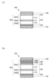
본 실시형태에서 설명하는 발광 디바이스(150)는 전극(551(i, j))과, 전극(552)과, EL층(553)을 가진다(도 1의 (A) 참조).The
전극(551(i, j))은 투과율(T1)을 가진다. 또한, 전극(552)은 전극(551(i, j))과 중첩되는 영역을 가지고, 전극(552)은 투과율(T2)을 가진다. 투과율(T2)은 투과율(T1)보다 높다. 또한, 전극(551(i, j))은 전극(552)보다 높은 반사율을 가진다.The electrode 551 (i, j) has transmittance T1. In addition, the
<EL층(553)의 구성예 1><Configuration Example 1 of
EL층(553)은 전극(551(i, j))과 전극(552) 사이에 끼워지는 영역을 가진다. 또한, EL층(553)은 영역(553A), 영역(553B), 및 영역(553C)을 가진다.The
영역(553A)은 영역(553B)과 영역(553C) 사이에 끼워지는 부분을 가진다. 또한, 영역(553A)은 발광성 재료를 포함하는 층(111) 및 층(111(12))을 포함한다.
영역(553B)은 전극(551(i, j))과 영역(553A) 사이에 끼워지는 영역을 가지고, 영역(553B)은 굴절률(n1)을 가진다.The
영역(553C)은 영역(553A)과 전극(552) 사이에 끼워지는 영역을 가지고, 영역(553C)은 굴절률(n2)을 가진다. 또한, 굴절률(n2)은 굴절률(n1)보다 낮다.The
<EL층(553)의 구성예 2><Configuration Example 2 of
EL층(553)은 유닛(103), 유닛(103(12)), 및 중간층(106)을 포함한다(도 1의 (A) 참조).The
<<중간층(106)의 구성예>><<Configuration Example of
중간층(106)은 유닛(103)과 유닛(103(12)) 사이에 끼워지고, 중간층(106)은 유닛(103) 및 유닛(103(12)) 중 한쪽에 정공을 공급하고, 다른 쪽에 전자를 공급하는 기능을 가진다.The
<<유닛(103)의 구성예 1>><<Structural example 1 of
유닛(103)은 전극(551(i, j))과 중간층(106) 사이에 끼워지고, 유닛(103)은 발광성 재료를 포함하는 층(111)을 가진다.The
<<유닛(103(12))의 구성예 1>><<Structural example 1 of unit 103 (12)>>
유닛(103(12))은 중간층(106)과 전극(552) 사이에 끼워지고, 유닛(103(12))은 발광성 재료를 포함하는 층(111(12))을 가진다.The unit 103(12) is sandwiched between the
<<영역(553A)의 구성예>><<Configuration Example of
영역(553A)은 발광성 재료를 포함하는 층(111) 및 발광성 재료를 포함하는 층(111(12))을 포함한다. 예를 들어, 발광성 재료를 포함하는 층(111(12))은 발광성 재료를 포함하는 층(111)과 전극(552) 사이에 끼워지는 영역을 가진다.
이에 의하여, 영역(553A)으로부터 사출되는 광을 전극(552)에서 효율적으로 추출할 수 있다. 또는, 전류 밀도를 낮게 유지하면서 고휘도 발광을 할 수 있게 할 수 있다. 또는 신뢰성을 향상시킬 수 있다. 또는 동일한 휘도로 비교하였을 때 구동 전압을 저감할 수 있다. 또는 소비 전력을 억제할 수 있다. 그 결과, 편의성, 유용성, 또는 신뢰성이 우수한 신규 광 기능 디바이스를 제공할 수 있다.In this way, the light emitted from the
<<유닛(103(12))의 구성예 2>><<Structural Example 2 of Unit 103 (12)>>
예를 들어, 유닛(103)이 사출하는 광과 같은 색의 광을 사출하는 구성을 유닛(103(12))에 사용할 수 있다. 구체적으로는, 청색광을 발하는 발광성 재료를, 발광성 재료를 포함하는 층(111) 및 발광성 재료를 포함하는 층(111(12))에 사용할 수 있다.For example, a structure that emits light of the same color as the light emitted by the
이에 의하여, 발광성 재료를 포함하는 층(111)으로부터 사출되는 광과, 발광성 재료를 포함하는 층(111(12))으로부터 사출되는 광이 서로를 강하게 하는 위치에 각 층을 배치할 수 있다. 또는, 발광성 재료를 포함하는 층으로부터 사출되는 광과, 전극(551(i, j))에서 반사된 광이 서로를 강하게 하는 위치에, 발광성 재료를 포함하는 층을 배치할 수 있다. 또는, 영역(553A)으로부터 사출되는 광을 전극(552)에서 효율적으로 추출할 수 있다. 그 결과, 편의성, 유용성, 또는 신뢰성이 우수한 신규 광 기능 디바이스를 제공할 수 있다.In this way, each layer can be disposed at a position where the light emitted from the
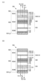
<<유닛(103(12))의 구성예 3>><<Structural Example 3 of Unit 103 (12)>>
유닛(103(12))은 발광성 재료를 포함하는 층(111(13))을 가진다(도 2의 (A) 참조). 예를 들어, 발광성 재료를 포함하는 층(111(12))은 발광성 재료를 포함하는 층(111)과 전극(552) 사이에 끼워지는 영역을 가지고, 발광성 재료를 포함하는 층(111(13))은 발광성 재료를 포함하는 층(111(12))과 전극(552) 사이에 끼워지는 영역을 가진다.The unit 103 (12) has a layer 111 (13) containing a luminescent material (see FIG. 2(A)). For example, the layer 111(12) including the light emitting material has a region sandwiched between the
<<발광성 재료를 포함하는 층의 구성예 1>><<Structural Example 1 of Layer Containing Light-Emitting Material>>
발광성 재료를 포함하는 층(111)은 청색광을 발하는 기능을 가지고, 발광성 재료를 포함하는 층(111(12))은 적색광을 발하는 기능을 가지고, 발광성 재료를 포함하는 층(111(13))은 녹색광을 발하는 기능을 가진다. 예를 들어, 발광성 재료를 포함하는 층(111(12))은 발광성 재료를 포함하는 층(111)과 전극(552) 사이에 끼워지는 영역을 가지고, 발광성 재료를 포함하는 층(111(13))은 발광성 재료를 포함하는 층(111)과 발광성 재료를 포함하는 층(111(12)) 사이에 끼워지는 영역을 가진다.The
이에 의하여, 영역(553A)으로부터 복수의 색의 광을 사출할 수 있다. 또는, 발광성 재료를 포함하는 층으로부터 사출되는 광과, 전극(551(i, j))에서 반사된 광이 서로를 강하게 하는 위치에, 발광성 재료를 포함하는 층을 배치할 수 있다. 또는, 발광성 재료를 포함하는 층으로부터 사출되는 광의 파장에 따라 발광성 재료를 포함하는 층을 배치할 수 있다. 또는, 연색성이 우수한 발광 디바이스를 제공할 수 있다. 또는, 영역(553A)으로부터 사출되는 광을 전극(552)에서 효율적으로 추출할 수 있다. 그 결과, 편의성, 유용성, 또는 신뢰성이 우수한 신규 광 기능 디바이스를 제공할 수 있다.In this way, light of a plurality of colors can be emitted from the
<발광 디바이스(150)의 구성예 2><Configuration Example 2 of Light-Emitting
또한, 본 실시형태에서 설명하는 발광 디바이스(150)는 전극(551(i, j))과, 전극(552)과, EL층(553)을 가진다(도 1의 (B) 참조).The
또한, 발광 디바이스(150)의 구성예 2는 전극(552)의 투과율(T2)이 전극(551(i, j))의 투과율(T1)보다 낮고, 영역(553B)의 굴절률(n1)이 영역(553C)의 굴절률(n2)보다 낮은 점에서, 도 1의 (A)를 참조하여 설명한 발광 디바이스와 다르다. 여기서는 상이한 부분에 대하여 자세히 설명하고, 같은 구성을 사용할 수 있는 부분에 대해서는 상술한 설명을 원용한다.Further, in Configuration Example 2 of the
이에 의하여, 영역(553A)으로부터 사출되는 광을 전극(551(i, j))에서 효율적으로 추출할 수 있다. 또는, 전류 밀도를 낮게 유지하면서 고휘도 발광을 할 수 있게 할 수 있다. 또는 신뢰성을 향상시킬 수 있다. 또는 동일한 휘도로 비교하였을 때 구동 전압을 저감할 수 있다. 또는 소비 전력을 억제할 수 있다. 그 결과, 편의성, 유용성, 또는 신뢰성이 우수한 신규 광 기능 디바이스를 제공할 수 있다.In this way, the light emitted from the
<<유닛(103(12))의 구성예 4>><<Structural Example 4 of Unit 103 (12)>>
예를 들어, 유닛(103)이 사출하는 광과 같은 색의 광을 사출하는 구성을 유닛(103(12))에 사용할 수 있다. 구체적으로는, 청색광을 발하는 발광성 재료를, 발광성 재료를 포함하는 층(111) 및 발광성 재료를 포함하는 층(111(12))에 사용할 수 있다.For example, a structure that emits light of the same color as the light emitted by the
이에 의하여, 발광성 재료를 포함하는 층(111)으로부터 사출되는 광과, 발광성 재료를 포함하는 층(111(12))으로부터 사출되는 광이 서로를 강하게 하는 위치에 각 층을 배치할 수 있다. 또는, 발광성 재료를 포함하는 층으로부터 사출되는 광과, 전극(552)에서 반사된 광이 서로를 강하게 하는 위치에, 발광성 재료를 포함하는 층을 배치할 수 있다. 또는, 영역(553A)으로부터 사출되는 광을 전극(551(i, j))에서 효율적으로 추출할 수 있다. 그 결과, 편의성, 유용성, 또는 신뢰성이 우수한 신규 광 기능 디바이스를 제공할 수 있다.In this way, each layer can be disposed at a position where the light emitted from the
<<유닛(103)의 구성예 2>><<Structural example 2 of
유닛(103)은 발광성 재료를 포함하는 층(111(13))을 가진다(도 2의 (B) 참조). 예를 들어, 발광성 재료를 포함하는 층(111(12))은 발광성 재료를 포함하는 층(111)과 전극(552) 사이에 끼워지는 영역을 가지고, 발광성 재료를 포함하는 층(111(13))은 발광성 재료를 포함하는 층(111)과 전극(551(i, j)) 사이에 끼워지는 영역을 가진다.The
<<발광성 재료를 포함한 층의 구성예 2>><<Structural Example 2 of Layer Containing Light-Emitting Material>>
발광성 재료를 포함하는 층(111)은 적색광을 발하는 기능을 가지고, 발광성 재료를 포함하는 층(111(12))은 청색광을 발하는 기능을 가지고, 발광성 재료를 포함하는 층(111(13))은 녹색광을 발하는 기능을 가진다.The
이에 의하여, 영역(553A)으로부터 복수의 색의 광을 사출할 수 있다. 또는, 발광성 재료를 포함하는 층으로부터 사출되는 광과, 전극(552)에서 반사된 광이 서로를 강하게 하는 위치에, 발광성 재료를 포함하는 층을 배치할 수 있다. 또는, 발광성 재료를 포함하는 층으로부터 사출되는 광의 파장에 따라 발광성 재료를 포함하는 층을 배치할 수 있다. 또는, 연색성이 우수한 발광 디바이스를 제공할 수 있다. 또는, 영역(553A)으로부터 사출되는 광을 전극(551(i, j))에서 효율적으로 추출할 수 있다. 그 결과, 편의성, 유용성, 또는 신뢰성이 우수한 신규 광 기능 디바이스를 제공할 수 있다.In this way, light of a plurality of colors can be emitted from the
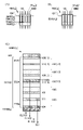
<발광 디바이스(150)의 구성예 3><Configuration Example 3 of Light-Emitting
또한, 본 실시형태에서 설명하는 발광 디바이스(150)는 전극(101)과, 전극(102)과, EL층(553)을 가진다(도 3의 (A) 참조). 전극(102)은 전극(101)과 중첩되는 영역을 가진다.In addition, the
EL층(553)은 전극(101)과 전극(102) 사이에 끼워지는 영역을 가진다. 또한, EL층(553)은 영역(553A), 영역(553B), 및 영역(553C)을 가진다. 영역(553A)은 영역(553B)과 영역(553C) 사이에 끼워지는 부분을 가진다.The
<발광 디바이스(150)의 구성예 4><Configuration Example 4 of Light-Emitting
또한, 본 실시형태에서 설명하는 발광 디바이스(150)는 전극(101)과, 전극(102)과, EL층(553)을 가진다(도 3의 (B) 참조). 또한, 영역(553C)이 중간층(106)을 가지는 점 및 중간층(106)이 전극(102)과 접하는 점에서, 도 3의 (A)를 참조하여 설명한 발광 디바이스와 다르다.In addition, the
또한, 본 실시형태는 본 명세서에서 설명하는 다른 실시형태와 적절히 조합할 수 있다.In addition, this embodiment can be suitably combined with other embodiments described in this specification.
(실시형태 2)(Embodiment 2)
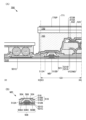
본 실시형태에서는, 본 발명의 일 형태의 발광 디바이스(150)의 구성에 대하여, 도 4 및 도 5를 참조하여 설명한다.In this embodiment, the configuration of the
도 4의 (A)는 본 발명의 일 형태의 발광 디바이스의 구성을 설명하는 도면이고, 도 4의 (B)는 도 4의 (A)와 다른 본 발명의 일 형태의 발광 디바이스의 구성을 설명하는 도면이다.Fig. 4(A) is a diagram explaining the configuration of a light emitting device of one embodiment of the present invention, and Fig. 4(B) explains the configuration of a light emitting device of one embodiment of the present invention different from Fig. 4(A). It is a drawing to
도 5의 (A)는 본 발명의 일 형태의 발광 디바이스의 구성을 설명하는 도면이고, 도 5의 (B)는 도 5의 (A)와 다른 본 발명의 일 형태의 발광 디바이스의 구성을 설명하는 도면이다.Fig. 5(A) is a diagram explaining the configuration of a light emitting device of one embodiment of the present invention, and Fig. 5(B) explains a configuration of a light emitting device of one embodiment of the present invention different from Fig. 5(A). It is a drawing to
<발광 디바이스(150)의 구성예 1><Configuration Example 1 of Light-Emitting
본 실시형태에서 설명하는 발광 디바이스(150)는 전극(551(i, j))과, 전극(552)과, EL층(553)을 가진다(도 4의 (A) 참조).The
전극(551(i, j))은 투과율(T1)을 가진다. 전극(552)은 전극(551(i, j))과 중첩되는 영역을 가지고, 전극(552)은 투과율(T2)을 가진다. 또한, 투과율(T2)은 투과율(T1)보다 높다. 또한, 전극(551(i, j))은 전극(552)보다 높은 반사율을 가진다.The electrode 551 (i, j) has transmittance T1. The
전극(551(i, j)) 및 전극(552) 중 어느 한쪽을 양극으로서 사용하고, 다른 쪽을 음극으로서 사용할 수 있다.Either one of the electrodes 551 (i, j) and the
예를 들어, 4.0eV 이상의 일함수를 가지는 재료를 양극에 적합하게 사용할 수 있다.For example, a material having a work function of 4.0 eV or higher can be suitably used for the anode.
예를 들어, 양극보다 일함수가 작은 재료를 음극에 사용할 수 있다. 구체적으로는, 3.8eV 이하의 일함수를 가지는 재료를 적합하게 사용할 수 있다.For example, a material having a smaller work function than the anode may be used for the cathode. Specifically, a material having a work function of 3.8 eV or less can be suitably used.
예를 들어, 원소 주기율표의 1족에 속하는 원소, 원소 주기율표의 2족에 속하는 원소, 희토류 금속, 및 이들을 포함하는 합금을 음극에 사용할 수 있다.For example, an element belonging to
구체적으로는, 리튬(Li), 세슘(Cs) 등, 마그네슘(Mg), 칼슘(Ca), 스트론튬(Sr) 등, 유로퓸(Eu), 이터븀(Yb) 등, 그리고 이들을 포함하는 합금(MgAg, AlLi)을 음극에 사용할 수 있다.Specifically, lithium (Li), cesium (Cs), magnesium (Mg), calcium (Ca), strontium (Sr), etc., europium (Eu), ytterbium (Yb), etc., and alloys containing them (MgAg , AlLi) can be used for the cathode.
<<전극(551(i, j))의 구성예 1>><<Configuration Example 1 of the electrode 551 (i, j)>>
예를 들어, 도전성 재료를 전극(551(i, j))에 사용할 수 있다. 또는, 반사막 및 도전막을 적층한 재료를 전극(551(i, j))에 사용할 수 있다.For example, a conductive material can be used for the electrode 551(i, j). Alternatively, a material in which a reflective film and a conductive film are laminated can be used for the electrode 551 (i, j).
구체적으로는, 금속, 합금, 도전성 화합물, 및 이들의 혼합물 등을 사용할 수 있다.Specifically, metals, alloys, conductive compounds, mixtures thereof, and the like can be used.
예를 들어 산화 인듐-산화 주석(ITO: Indium Tin Oxide), 실리콘 또는 산화 실리콘을 함유한 산화 인듐-산화 주석, 산화 인듐-산화 아연, 산화 텅스텐 및 산화 아연을 함유한 산화 인듐(IWZO) 등을 사용할 수 있다.Examples include indium tin oxide (ITO), indium oxide-tin oxide containing silicon or silicon oxide, indium oxide-zinc oxide, indium oxide containing tungsten oxide and zinc oxide (IWZO), etc. can be used
예를 들어 금(Au), 백금(Pt), 니켈(Ni), 텅스텐(W), 크로뮴(Cr), 몰리브데넘(Mo), 철(Fe), 코발트(Co), 구리(Cu), 팔라듐(Pd), 또는 금속 재료의 질화물(예를 들어 질화 타이타늄) 등을 사용할 수 있다. 또는 그래핀을 사용할 수 있다.For example, gold (Au), platinum (Pt), nickel (Ni), tungsten (W), chromium (Cr), molybdenum (Mo), iron (Fe), cobalt (Co), copper (Cu), Palladium (Pd) or a nitride of a metal material (for example, titanium nitride) or the like can be used. Alternatively, graphene may be used.
<<전극(552)의 구성예 1>><<Configuration Example 1 of
금속, 합금, 전기 전도성 화합물, 및 이들의 혼합물 등을 전극(552)에 사용할 수 있다.Metals, alloys, electrically conductive compounds, and mixtures thereof may be used for
<<EL층(553)의 구성예 1>><<Configuration Example 1 of
EL층(553)은 전극(551(i, j))과 전극(552) 사이에 끼워지는 영역을 가진다(도 4의 (A) 참조). 또한, EL층(553)은 영역(553A), 영역(553B), 및 영역(553C)을 가진다. 또한, 영역(553A)은 영역(553B)과 영역(553C) 사이에 끼워지는 부분을 가진다.The
또한, EL층(553)은 유닛(103), 유닛(103(12)), 층(104), 층(105), 층(105(12)), 및 중간층(106)을 가진다. 유닛(103)은 층(111), 층(112), 및 층(113)을 가진다. 유닛(103(12))은 층(111(12)), 층(111(13)), 층(112(12)), 및 층(113(12))을 가진다. 중간층(106)은 층(106A) 및 층(106B)을 가진다.Further, the
<<영역(553C)의 구성예 1>><<Configuration example 1 of
영역(553C)의 굴절률 n2가 영역(553B)의 굴절률 n1보다 낮아지고, 영역(553C)의 전자 수송성이 영역(553B)의 전자 수송성보다 높아지는 재료를 영역(553C)에 사용할 수 있다(도 4의 (A) 참조). 영역(553C)의 굴절률 n2를 낮춤으로써, 발광 디바이스(150)의 광 추출 효율을 높일 수 있다. 또한, 굴절률 n2와 굴절률 n1의 차이는 0.05 이상이 바람직하고, 0.1 이상이 더 바람직하고, 0.15 이상이 더욱 바람직하다. 또한, 영역(553C)은 층(113(12)) 및 층(105(12))을 가진다.A material in which the refractive index n2 of the
본 실시형태에서 설명하는 발광 디바이스(150)는 전극(551(i, j))을 양극으로서 사용하고, 전극(552)을 음극으로서 사용할 수 있다. 또한, 중간층(106)은 전자를 유닛(103)에 공급하고, 정공을 유닛(103(12))에 공급할 수 있다.In the
예를 들어, 청색 발광 영역(455nm 이상 465nm 이하)에서의 정상광 굴절률이 1.50 이상 1.75 이하, 또는 일반적으로 굴절률의 측정에 사용되는 633nm의 광에 대한 정상광 굴절률이 1.45 이상 1.70 이하인 전자 수송성을 가지는 재료를 영역(553C)에 사용할 수 있다.For example, the normal light refractive index in the blue light emitting region (455 nm or more and 465 nm or less) is 1.50 or more and 1.75 or less, or the normal light refractive index for light of 633 nm, which is generally used for refractive index measurement, is 1.45 or more and 1.70 or less. A material may be used for
또한, 재료에 이방성이 생긴 경우, 정상광에 대한 굴절률과 이상광에 대한 굴절률이 다른 경우가 있다. 측정하는 박막이 그러한 상태인 경우, 이방성 해석을 실시함으로써 정상광 굴절률과 이상광 굴절률로 분리하여 각각의 굴절률을 산출할 수 있다. 또한 본 명세서에 있어서는 측정한 재료에 정상광 굴절률과 이상광 굴절률의 양쪽이 존재한 경우, 정상광 굴절률을 지표로서 사용한다.Further, when anisotropy occurs in the material, the refractive index for normal light and the refractive index for extraordinary light may differ. When the thin film to be measured is in such a state, it is possible to calculate the respective refractive indices by separating them into normal light refractive index and extraordinary light refractive index by performing anisotropic analysis. In addition, in this specification, when both a normal light refractive index and an extraordinary light refractive index exist in the measured material, the normal light refractive index is used as an index.
[전자 수송성을 가지는 재료][Materials having electron transport properties]
상기 전자 수송성을 가지는 재료의 하나로서는, 하나 이상 3개 이하의 질소를 포함하는 6원 고리의 헤테로 방향족 고리를 적어도 하나 가지고, 고리를 형성하는 탄소수가 6 내지 14의 방향족 탄화수소 고리를 복수로 가지고, 복수의 상기 방향족 탄화수소 고리 중 적어도 2개는 벤젠 고리이고, sp3 혼성 궤도로 결합을 형성하는 탄화수소기를 복수로 가지는 유기 화합물을 들 수 있다.As one of the electron-transporting materials, it has at least one six-membered heteroaromatic ring containing one or more and three or fewer nitrogen atoms, and has a plurality of aromatic hydrocarbon rings having 6 to 14 carbon atoms forming the ring, At least two of the plurality of aromatic hydrocarbon rings are benzene rings, and organic compounds having a plurality of hydrocarbon groups forming bonds with sp3 hybrid orbitals are exemplified.
또한, 이와 같은 유기 화합물은 상기 유기 화합물의 분자 내의 총탄소수에 대한, sp3 혼성 궤도로 결합을 형성하는 탄소수의 비율이 10% 이상 60% 이하인 것이 바람직하고, 10% 이상 50% 이하인 것이 더 바람직하다. 또는, 이와 같은 유기 화합물은 1H-NMR로 상기 유기 화합물의 측정을 한 결과에 있어서의 4ppm 미만의 시그널의 적분값이 4ppm 이상의 시그널의 적분값의 1/2배 이상인 것이 바람직하다.Further, in such an organic compound, the ratio of the number of carbon atoms bonded to the sp3 hybrid orbital to the total number of carbon atoms in the molecule of the organic compound is preferably 10% or more and 60% or less, more preferably 10% or more and 50% or less. . Alternatively, it is preferable that the integral of the signal of less than 4 ppm in the result of measuring the organic compound by 1 H-NMR is 1/2 times or more of the integral of the signal of 4 ppm or more.
또한, 상기 유기 화합물이 가지는 sp3 혼성 궤도로 결합을 형성하는 탄화수소기는 모두 상기 고리를 형성하는 탄소수가 6 내지 14의 방향족 탄화수소 고리에 결합되고, 그 방향족 탄화수소 고리에는 상기 유기 화합물의 LUMO가 분포되지 않는 것이 바람직하다.In addition, all hydrocarbon groups forming bonds with sp3 hybrid orbitals of the organic compound are bonded to an aromatic hydrocarbon ring having 6 to 14 carbon atoms forming the ring, and the LUMO of the organic compound is not distributed in the aromatic hydrocarbon ring. it is desirable
상기 전자 수송성을 가지는 유기 화합물로서는, 하기 일반식(Ge11 또는 Ge12)으로 나타내어지는 유기 화합물이 바람직하다.As the organic compound having the electron transport property, an organic compound represented by the following general formula (
[화학식 1][Formula 1]

식 중에서 A는 하나 이상 3개 이하의 질소를 포함하는 6원 고리의 헤테로 방향족 고리를 나타내고, 피리딘 고리, 피리미딘 고리, 피라진 고리, 피리다진 고리, 트라이아진 고리 중 어느 것인 것이 바람직하다.In the formula, A represents a six-membered heteroaromatic ring containing one or more and three nitrogen atoms, and is preferably any one of a pyridine ring, a pyrimidine ring, a pyrazine ring, a pyridazine ring, and a triazine ring.
또한, R200은 수소, 탄소수 1 내지 6의 알킬기, 탄소수 3 내지 10의 지환식기, 또는 식(Gel1-1)으로 나타내어지는 치환기 중 어느 것을 나타낸다.Further, R 200 represents hydrogen, an alkyl group having 1 to 6 carbon atoms, an alicyclic group having 3 to 10 carbon atoms, or a substituent represented by formula (G el 1-1).
R201 내지 R215 중 적어도 하나는 치환기를 가지는 페닐기이고, 나머지는 각각 독립적으로 수소, 탄소수 1 내지 6의 알킬기, 탄소수 3 내지 10의 지환식기, 치환 또는 비치환된 고리를 형성하는 탄소수가 6 내지 14의 방향족 탄화수소기, 치환 또는 비치환된 피리딜기 중 어느 것을 나타낸다. 또한, R201, R203, R205, R206, R208, R210, R211, R213 및 R215는 수소인 것이 바람직하다. 상기 치환기를 가지는 페닐기는 하나 또는 2개의 치환기를 가지고, 상기 치환기는 각각 독립적으로 탄소수 1 내지 6의 알킬기, 탄소수 3 내지 10의 지환식기, 치환 또는 비치환된 고리를 형성하는 탄소수가 6 내지 14의 방향족 탄화수소기 중 어느 것이다.At least one of R 201 to R 215 is a phenyl group having a substituent, and the others are each independently hydrogen, an alkyl group having 1 to 6 carbon atoms, an alicyclic group having 3 to 10 carbon atoms, or a substituted or unsubstituted ring having 6 to 6 carbon atoms forming a ring. 14 represents any of an aromatic hydrocarbon group and a substituted or unsubstituted pyridyl group. Further, R 201 , R 203 , R 205 , R 206 , R 208 , R 210 , R 211 , R 213 and R 215 are preferably hydrogen. The phenyl group having the substituent has one or two substituents, and the substituents are each independently an alkyl group having 1 to 6 carbon atoms, an alicyclic group having 3 to 10 carbon atoms, and a substituted or unsubstituted ring having 6 to 14 carbon atoms forming a ring. any of the aromatic hydrocarbon groups.
또한, 상기 일반식(Ge11)으로 나타내어지는 유기 화합물은 탄소수 1 내지 6의 알킬기, 및 탄소수 3 내지 10의 지환식기로부터 선택되는 탄화수소기를 복수로 가지고, 분자 내의 총탄소수에 대한, sp3 혼성 궤도로 결합을 형성하는 총탄소수의 비율은 10% 이상 60% 이하이다.In addition, the organic compound represented by the general formula (G e1 1) has a plurality of hydrocarbon groups selected from an alkyl group having 1 to 6 carbon atoms and an alicyclic group having 3 to 10 carbon atoms, and has an sp3 hybrid orbital with respect to the total number of carbon atoms in the molecule. The proportion of the total number of carbon atoms forming bonds with is 10% or more and 60% or less.
또한, 상기 전자 수송성을 가지는 유기 화합물로서는, 하기 일반식(Ge12)으로 나타내어지는 유기 화합물이 바람직하다.As the organic compound having the electron transport property, an organic compound represented by the following general formula (G e1 2 ) is preferable.
[화학식 2][Formula 2]

식 중에서 Q1 내지 Q3 중 2개 또는 3개는 N을 나타내고, 상기 Q1 내지 Q3 중 2개가 N인 경우, 나머지 하나는 CH를 나타낸다.In the formula, two or three of Q 1 to Q 3 represent N, and when two of Q 1 to Q 3 are N, the other represents CH.
또한, R201 내지 R215 중 적어도 어느 하나는 치환기를 가지는 페닐기이고, 나머지는 각각 독립적으로 수소, 탄소수 1 내지 6의 알킬기, 탄소수 3 내지 10의 지환식기, 치환 또는 비치환된 고리를 형성하는 탄소수가 6 내지 14의 방향족 탄화수소기, 치환 또는 비치환된 피리딜기 중 어느 것을 나타낸다. 또한, R201, R203, R205, R206, R208, R210, R211, R213 및 R215는 수소인 것이 바람직하다. 상기 치환기를 가지는 페닐기는 하나 또는 2개의 치환기를 가지고, 상기 치환기는 각각 독립적으로 탄소수 1 내지 6의 알킬기, 탄소수 3 내지 10의 지환식기, 치환 또는 비치환된 고리를 형성하는 탄소수가 6 내지 14의 방향족 탄화수소기 중 어느 것이다.In addition, at least one of R 201 to R 215 is a phenyl group having a substituent, and the others are each independently hydrogen, an alkyl group having 1 to 6 carbon atoms, an alicyclic group having 3 to 10 carbon atoms, and carbon atoms forming a substituted or unsubstituted ring represents any of 6 to 14 aromatic hydrocarbon groups and substituted or unsubstituted pyridyl groups. Further, R 201 , R 203 , R 205 , R 206 , R 208 , R 210 , R 211 , R 213 and R 215 are preferably hydrogen. The phenyl group having the substituent has one or two substituents, and the substituents are each independently an alkyl group having 1 to 6 carbon atoms, an alicyclic group having 3 to 10 carbon atoms, and a substituted or unsubstituted ring having 6 to 14 carbon atoms forming a ring. any of the aromatic hydrocarbon groups.
또한, 상기 일반식(Ge12)으로 나타내어지는 유기 화합물은 탄소수 1 내지 6의 알킬기, 및 탄소수 3 내지 10의 지환식기로부터 선택되는 탄화수소기를 복수로 가지고, 분자 내의 총탄소수에 대한 sp3 혼성 궤도로 결합을 형성하는 탄소수의 비율은 10% 이상 60% 이하인 것이 바람직하다.In addition, the organic compound represented by the general formula (G e1 2) has a plurality of hydrocarbon groups selected from an alkyl group having 1 to 6 carbon atoms and an alicyclic group having 3 to 10 carbon atoms, and has an sp3 hybrid orbital with respect to the total number of carbon atoms in the molecule. It is preferable that the ratio of carbon number forming a bond is 10% or more and 60% or less.
또한, 상기 일반식(Ge11 또는 Ge12)으로 나타내어지는 유기 화합물에서, 치환기를 가지는 페닐기가 하기 식(Ge11-2)으로 나타내어지는 기인 것이 바람직하다.In addition, in the organic compound represented by the general formula (
[화학식 3][Formula 3]

식 중에서 α는 치환 또는 비치환된 페닐렌기를 나타내고, 메타 위치 치환된 페닐렌기인 것이 바람직하다. 또한, 메타 위치 치환된 페닐렌기가 치환기를 하나 가지는 경우, 상기 치환기도 메타 위치에 치환된 것이 바람직하다. 또한, 상기 치환기로서는 탄소수 1 내지 6의 알킬기, 또는 탄소수 3 내지 10의 지환식기인 것이 바람직하고, 탄소수 1 내지 6의 알킬기인 것이 더 바람직하고, t-뷰틸기인 것이 더욱 바람직하다.In the formula, α represents a substituted or unsubstituted phenylene group, and is preferably a meta-substituted phenylene group. In addition, when the phenylene group substituted at the meta position has one substituent, it is preferable that the substituent is also substituted at the meta position. The substituent is preferably an alkyl group of 1 to 6 carbon atoms or an alicyclic group of 3 to 10 carbon atoms, more preferably an alkyl group of 1 to 6 carbon atoms, and still more preferably a t-butyl group.
R220은 탄소수 1 내지 6의 알킬기, 탄소수 3 내지 10의 지환식기, 또는 치환 또는 비치환된 고리를 형성하는 탄소수가 6 내지 14의 방향족 탄화수소기를 나타낸다.R 220 represents an alkyl group having 1 to 6 carbon atoms, an alicyclic group having 3 to 10 carbon atoms, or an aromatic hydrocarbon group having 6 to 14 carbon atoms forming a substituted or unsubstituted ring.
또한, j 및 k는 1 내지 2를 나타낸다. 또한, j가 2인 경우, 복수의 α는 각각 같아도 좋고 달라도 좋다. 또한, k가 2인 경우, 복수의 R220은 각각 같아도 좋고 달라도 좋다. 또한, R220은 페닐기인 것이 바람직하고, 두 군데의 메타 위치 중 한쪽 또는 양쪽에 탄소수 1 내지 6의 알킬기, 또는 탄소수 3 내지 10의 지환식기를 가지는 페닐기이다. 또한, 상기 페닐기가 두 군데의 메타 위치 중 한쪽 또는 양쪽에 가지는 치환기는 탄소수 1 내지 6의 알킬기인 것이 더 바람직하고, t-뷰틸기인 것이 더욱 바람직하다.Moreover, j and k represent 1-2. In addition, when j is 2, a plurality of α may be the same or different. In addition, when k is 2, a plurality of R 220 may be the same or different. Further, R 220 is preferably a phenyl group, and is a phenyl group having an alkyl group having 1 to 6 carbon atoms or an alicyclic group having 3 to 10 carbon atoms at one or both of the two meta positions. Further, the substituents at one or both of the two meta positions of the phenyl group are more preferably an alkyl group having 1 to 6 carbon atoms, and more preferably a t-butyl group.
구체적으로는, 2-{(3',5'-다이-tert-뷰틸)-1,1'-바이페닐-3-일}-4,6-비스(3,5-다이-tert-뷰틸페닐)-1,3,5-트라이아진(약칭: mmtBumBP-dmmtBuPTzn), 2-{(3',5'-다이-tert-뷰틸)-1,1'-바이페닐-3-일}-4,6-다이페닐-1,3,5-트라이아진(약칭: mmtBumBPTzn), 2-(3,3'',5,5''-테트라-tert-뷰틸-1,1':3',1''-페닐-5'-일)-4,6-다이페닐-1,3,5-트라이아진(약칭: mmtBumTPTzn), 2-{(3',5'-다이-tert-뷰틸)-1,1'-바이페닐-3-일}-4,6-비스(3,5-다이-tert-뷰틸페닐)-1,3-피리미딘(약칭: mmtBumBP-dmmtBuPPm), 2-(3,3'',5',5''-테트라-tert-뷰틸-1,1':3',1''-터페닐-5-일)-4,6-다이페닐-1,3,5-트라이아진(약칭: mmtBumTPTzn-02) 등을 영역(553C)에 사용할 수 있다.Specifically, 2-{(3',5'-di-tert-butyl)-1,1'-biphenyl-3-yl}-4,6-bis(3,5-di-tert-butylphenyl )-1,3,5-triazine (abbreviation: mmtBumBP-dmmtBuPTzn), 2-{(3',5'-di-tert-butyl)-1,1'-biphenyl-3-yl}-4, 6-diphenyl-1,3,5-triazine (abbreviation: mmtBumBPTzn), 2-(3,3'',5,5''-tetra-tert-butyl-1,1':3',1' '-phenyl-5'-yl)-4,6-diphenyl-1,3,5-triazine (abbreviation: mmtBumTPTzn), 2-{(3',5'-di-tert-butyl)-1, 1'-biphenyl-3-yl} -4,6-bis (3,5-di-tert-butylphenyl) -1,3-pyrimidine (abbreviation: mmtBumBP-dmmtBuPPm), 2- (3,3' ',5',5''-tetra-tert-butyl-1,1':3',1''-terphenyl-5-yl)-4,6-diphenyl-1,3,5-triazine (abbreviation: mmtBumTPTzn-02) or the like can be used for the region 553C.
<<EL층(553)의 구성예 2>><<Structural Example 2 of
또한, EL층(553)은 유닛(103), 유닛(103(12)), 층(105), 층(105(12)), 층(104(12)), 및 중간층(106)을 가진다(도 5의 (A) 참조). 유닛(103)은 층(111), 층(112), 및 층(113)을 가진다. 유닛(103(12))은 층(111(12)), 층(111(13)), 층(112(12)), 및 층(113(12))을 가진다. 중간층(106)은 층(106A) 및 층(106B)을 가진다.Further, the
<<영역(553C)의 구성예 2>><<Configuration example 2 of
또한, 영역(553C)의 굴절률 n2가 영역(553B)의 굴절률 n1보다 낮아지고, 영역(553C)의 정공 수송성이 영역(553B)의 정공 수송성보다 높아지는 재료를 영역(553C)에 사용할 수 있다(도 5의 (A) 참조). 영역(553C)의 굴절률 n2를 낮춤으로써, 발광 디바이스(150)의 광 추출 효율을 높일 수 있다. 또한, 굴절률 n2와 굴절률 n1의 차이는 0.05 이상이 바람직하고, 0.1 이상이 더 바람직하고, 0.15 이상이 더욱 바람직하다. 또한, 본 실시형태에서 설명하는 발광 디바이스(150)는 전극(551(i, j))을 음극으로서 사용하고, 전극(552)을 양극으로서 사용할 수 있다. 또한, 중간층(106)은 정공을 유닛(103)에 공급하고, 전자를 유닛(103(12))에 공급할 수 있다.Further, a material in which the refractive index n2 of the
예를 들어, 청색 발광 영역(455nm 이상 465nm 이하)에서의 정상광 굴절률이 1.50 이상 1.75 이하, 또는 일반적으로 굴절률의 측정에 사용되는 633nm의 광에 대한 정상광 굴절률이 1.45 이상 1.70 이하인 정공 수송성을 가지는 재료를 영역(553C)에 사용할 수 있다.For example, the normal light refractive index in the blue light emitting region (455 nm or more and 465 nm or less) is 1.50 or more and 1.75 or less, or the normal light refractive index for light of 633 nm, which is generally used for refractive index measurement, is 1.45 or more and 1.70 or less. A material may be used for
[정공 수송성을 가지는 재료][Materials having hole transport properties]
상기 정공 수송성을 가지는 재료의 하나로서는, 제 1 방향족기, 제 2 방향족기, 및 제 3 방향족기를 가지고, 이들 제 1 방향족기, 제 2 방향족기, 및 제 3 방향족기가 동일한 질소 원자에 결합된 모노아민 화합물을 들 수 있다.As one of the above hole-transporting materials, it has a first aromatic group, a second aromatic group, and a third aromatic group, and these first aromatic groups, second aromatic groups, and third aromatic groups are bonded to the same nitrogen atom. An amine compound is mentioned.
상기 모노아민 화합물은 분자 내의 총탄소수에 대한, sp3 혼성 궤도로 결합을 형성하는 탄소의 비율이 23% 이상 55% 이하인 것이 바람직하고, 또한 1H-NMR로 상기 모노아민 화합물을 측정한 결과에 있어서의 4ppm 미만의 시그널의 적분값이 4ppm 이상의 시그널의 적분값을 웃도는 화합물인 것이 바람직하다.The monoamine compound preferably has a ratio of 23 % or more to 55% or less of carbon that forms a bond with an sp3 hybridized orbital relative to the total number of carbon atoms in the molecule. It is preferable that the integral value of the signal of less than 4 ppm of the compound exceeds the integral value of the signal of 4 ppm or more.
또한, 상기 모노아민 화합물은 적어도 하나의 플루오렌 골격을 가지고, 상기 제 1 방향족기, 상기 제 2 방향족기, 및 상기 제 3 방향족기 중 어느 하나 또는 복수가 플루오렌 골격인 것이 바람직하다.In addition, it is preferable that the monoamine compound has at least one fluorene skeleton, and any one or a plurality of the first aromatic group, the second aromatic group, and the third aromatic group have a fluorene skeleton.
이상과 같은 정공 수송성을 가지는 재료의 예로서는, 이하의 일반식(Gh11 내지 Gh14)과 같은 구조를 가지는 유기 화합물을 들 수 있다.Examples of materials having the above hole-transporting properties include organic compounds having structures such as the following general formulas (
[화학식 4][Formula 4]

상기 일반식(Gh11)에 있어서 Ar1, Ar2는 각각 독립적으로 벤젠 고리, 또는 2개 또는 3개의 벤젠 고리가 서로 결합된 치환기를 나타낸다. 다만, Ar1 및 Ar2 중 한쪽 또는 양쪽은 탄소가 sp3 혼성 궤도만으로 결합을 형성하는 탄소수 1 내지 12의 탄화수소기를 하나 또는 복수로 가지고, Ar1 및 Ar2에 결합된 모든 상기 탄화수소기에 포함되는 탄소의 총수가 8개 이상이고, 또한 Ar1 및 Ar2 중 어느 한쪽에 결합된 모든 상기 탄화수소기에 포함되는 탄소의 총수가 6개 이상이다. 또한, Ar1 또는 Ar2에 상기 탄화수소기로서 탄소수 1 내지 2의 직쇄 알킬기가 복수 결합되어 있는 경우, 상기 직쇄 알킬기끼리가 결합하여 고리를 형성하여도 좋다.In the general formula (G h1 1), Ar 1 and Ar 2 each independently represent a benzene ring or a substituent in which two or three benzene rings are bonded to each other. However, one or both of Ar 1 and Ar 2 has one or a plurality of hydrocarbon groups having 1 to 12 carbon atoms in which carbon forms a bond only with sp3 hybrid orbitals, and carbons included in all the hydrocarbon groups bonded to Ar 1 and Ar 2 The total number of is 8 or more, and the total number of carbons included in all the hydrocarbon groups bonded to either one of Ar 1 and Ar 2 is 6 or more. Further, when a plurality of straight-chain alkyl groups having 1 to 2 carbon atoms are bonded to Ar 1 or Ar 2 as the hydrocarbon group, the straight-chain alkyl groups may bond to each other to form a ring.
[화학식 5][Formula 5]

상기 일반식(Gh12)에 있어서, m 및 r는 각각 독립적으로 1 또는 2를 나타내고, m+r는 2 또는 3이다. 또한, t는 0 내지 4의 정수를 나타내고, 0인 것이 바람직하다. 또한, R5는 수소 또는 탄소수 1 내지 3의 탄화수소기 중 어느 것을 나타낸다. 또한, m이 2인 경우 2개의 페닐렌기가 가지는 치환기의 종류, 치환기의 개수, 및 결합손의 위치는 같아도 좋고 달라도 좋고, r가 2인 경우 2개의 페닐기가 가지는 치환기의 종류, 치환기의 개수, 및 결합손의 위치는 같아도 좋고 달라도 좋다. 또한, t가 2 내지 4의 정수인 경우, 복수의 R5는 각각 같아도 좋고 달라도 좋고, R5는 인접한 기가 서로 결합하여 고리를 형성하여도 좋다.In the above general formula (G h1 2), m and r each independently represent 1 or 2, and m+r is 2 or 3. Further, t represents an integer of 0 to 4, and is preferably 0. Further, R 5 represents either hydrogen or a hydrocarbon group having 1 to 3 carbon atoms. In addition, when m is 2, the types of substituents possessed by the two phenylene groups, the number of substituents, and the position of the bond may be the same or different, and when r is 2, the types of substituents possessed by the two phenylene groups, the number of substituents, and the position of the bonding hand may be the same or different. Further, when t is an integer of 2 to 4, a plurality of R 5 ' s may be the same or different, and adjacent groups of R 5 may bond to each other to form a ring.
[화학식 6][Formula 6]

상기 일반식(Gh12 및 Gh13)에 있어서, n 및 p는 각각 독립적으로 1 또는 2를 나타내고, n+p는 2 또는 3이다. s는 0 내지 4의 정수를 나타내고, 0인 것이 바람직하다. 또한, R4는 수소 또는 탄소수 1 내지 3의 탄화수소기 중 어느 것을 나타내고, 또한 n이 2인 경우 2개의 페닐렌기가 가지는 치환기의 종류, 치환기의 개수, 및 결합손의 위치는 같아도 좋고 달라도 좋고, p가 2인 경우 2개의 페닐기가 가지는 치환기의 종류, 치환기의 개수, 및 결합손의 위치는 같아도 좋고 달라도 좋다. 또한, s가 2 내지 4의 정수인 경우, 복수의 R4는 각각 같아도 좋고 달라도 좋다.In the general formulas (
[화학식 7][Formula 7]

상기 일반식(Gh12 내지 Gh14)에 있어서, R10 내지 R14 및 R20 내지 R24는 각각 독립적으로 수소 또는 탄소가 sp3 혼성 궤도만으로 결합을 형성하는 탄소수 1 내지 12의 탄화수소기를 나타낸다. 또한, R10 내지 R14 중 적어도 3개 및 R20 내지 R24 중 적어도 3개가 수소인 것이 바람직하다. 탄소가 sp3 혼성 궤도만으로 결합을 형성하는 탄소수 1 내지 12의 탄화수소기로서는, tert-뷰틸기 및 사이클로헥실기가, 분자 굴절률을 낮출 수 있어 바람직하다. 다만, R10 내지 R14 및 R20 내지 R24에 포함되는 탄소의 총수는 8개 이상이고, 또한 R10 내지 R14 및 R20 내지 R24 중 어느 한쪽에 포함되는 탄소의 총수가 6개 이상인 것으로 한다. R4, R10 내지 R14, 및 R20 내지 R24는 인접한 기가 서로 결합하여 고리를 형성하여도 좋다.In the above general formula (
또한, 상기 일반식(Gh11 내지 Gh14)에 있어서, u는 0 내지 4의 정수를 나타내고, 0인 것이 바람직하다. u가 2 내지 4의 정수인 경우, 복수의 R3은 각각 같아도 좋고 달라도 좋다. 또한, R1, R2, 및 R3은 각각 독립적으로 탄소수 1 내지 4의 알킬기를 나타내고, R1 및 R2는 서로 결합하여 고리를 형성하여도 좋다.In the general formulas (
또한, 상기 정공 수송성을 가지는 재료 중 하나로서는, 적어도 하나의 방향족기를 가지고, 상기 방향족기는 제 1 벤젠 고리 내지 제 3 벤젠 고리와, 적어도 3개의 알킬기를 가지는 아릴아민 화합물인 것이 바람직하다. 또한, 제 1 벤젠 고리 내지 제 3 벤젠 고리는 이 순서대로 결합되고, 제 1 벤젠 고리가 아민의 질소에 직접 결합된 것으로 한다.Moreover, as one of the materials having the hole transport property, it is preferable that the aromatic group is an arylamine compound having at least one aromatic group, and the aromatic group has first to third benzene rings and at least three alkyl groups. In addition, it is assumed that the first benzene ring to the third benzene ring are bonded in this order, and the first benzene ring is bonded directly to the nitrogen of the amine.
또한, 제 1 벤젠 고리는 치환 또는 비치환된 페닐기를 더 가져도 좋고, 비치환된 페닐기를 가지는 것이 바람직하다. 또한, 상기 제 2 벤젠 고리 또는 상기 제 3 벤젠 고리가 알킬기로 치환된 페닐기를 가져도 좋다.In addition, the first benzene ring may further have a substituted or unsubstituted phenyl group, and preferably has an unsubstituted phenyl group. Further, the second benzene ring or the third benzene ring may have a phenyl group substituted with an alkyl group.
또한, 상기 제 1 벤젠 고리 내지 상기 제 3 벤젠 고리 중 2개 이상의 벤젠 고리, 바람직하게는 모든 벤젠 고리의 1위치 및 3위치의 탄소에는 수소는 직접 결합되지 않고, 상술한 제 1 벤젠 고리 내지 제 3 벤젠 고리, 상술한 알킬기로 치환된 페닐기, 상술한 적어도 3개의 알킬기, 및 상술한 아민의 질소 중 어느 것이 결합된 것으로 한다.In addition, hydrogen is not directly bonded to carbons at
또한, 상기 아릴아민 화합물은 제 2 방향족기를 더 가지는 것이 바람직하다. 제 2 방향족기로서는 비치환된 단일 고리, 또는 치환 또는 비치환된 고리가 3개 이하의 축합 고리를 가지는 기인 것이 바람직하고, 이들 중에서도 치환 또는 비치환된 고리가 3개 이하의 축합 고리이고, 상기 축합 고리가 고리를 형성하는 탄소수가 6 내지 13의 축합 고리를 가지는 기인 것이 더 바람직하고, 플루오렌 고리를 가지는 기인 것이 더욱 바람직하다. 또한, 제 2 방향족기로서는 다이메틸플루오렌일기가 바람직하다.Also, the arylamine compound preferably further has a second aromatic group. The second aromatic group is preferably a group having an unsubstituted single ring or a substituted or unsubstituted ring having three or less condensed rings, and among these, a substituted or unsubstituted ring is a condensed ring of three or less. It is more preferable that the condensed ring is a group having a condensed ring having 6 to 13 carbon atoms forming the ring, and a group having a fluorene ring is still more preferable. Moreover, as a 2nd aromatic group, a dimethyl fluorenyl group is preferable.
또한, 상기 아릴아민 화합물은 제 3 방향족기를 더 가지는 것이 바람직하다. 제 3 방향족기는 치환 또는 비치환된 벤젠 고리를 하나 내지 3개 가지는 기이다.Also, the arylamine compound preferably further has a third aromatic group. The third aromatic group is a group having one to three substituted or unsubstituted benzene rings.
상술한 적어도 3개의 알킬기, 페닐기로 치환되는 알킬기는, 탄소수 2 내지 5의 쇄식 알킬기인 것이 바람직하다. 특히 상기 알킬기로서는 탄소수 3 내지 5의 분기를 가지는 쇄식 알킬기가 바람직하고, t-뷰틸기가 더 바람직하다.It is preferable that the alkyl group substituted with the above-mentioned at least 3 alkyl group or phenyl group is a C2-C5 chained alkyl group. Particularly, as the alkyl group, a branched chain alkyl group having 3 to 5 carbon atoms is preferable, and a t-butyl group is more preferable.
이상과 같은 정공 수송성을 가지는 재료의 예로서는, 하기 (Gh21 내지 Gh23)과 같은 구조를 가지는 유기 화합물을 들 수 있다.Examples of materials having the above hole-transporting properties include organic compounds having structures as described below (
[화학식 8][Formula 8]

또한, 상기 일반식(Gh21)에 있어서, Ar101은 치환 또는 비치환된 벤젠 고리, 또는 2개 또는 3개의 치환 또는 비치환된 벤젠 고리가 서로 결합된 치환기를 나타낸다.Also, in the general formula (G h2 1), Ar 101 represents a substituted or unsubstituted benzene ring or a substituent in which two or three substituted or unsubstituted benzene rings are bonded to each other.
[화학식 9][Formula 9]

또한, 상기 일반식(Gh22)에 있어서, x 및 y는 각각 독립적으로 1 또는 2를 나타내고, x+y는 2 또는 3이다. 또한, R109는 탄소수 1 내지 4의 알킬기를 나타내고, w는 0 내지 4의 정수를 나타낸다. 또한, R141 내지 R145는 각각 독립적으로 수소, 탄소수 1 내지 6의 알킬기, 탄소수 5 내지 12의 사이클로알킬기 중 어느 하나를 나타낸다. w가 2 이상인 경우, 복수의 R109는 각각 같아도 좋고 달라도 좋다. 또한, x가 2인 경우, 2개의 페닐렌기가 가지는 치환기의 종류, 치환기의 개수, 및 결합손의 위치는 같아도 좋고 달라도 좋다. 또한, y사 2인 경우, 2개의 R141 내지 R145를 가지는 페닐기가 가지는 치환기의 종류, 및 치환기의 개수는 같아도 좋고 달라도 좋다.In addition, in the above general formula (G h2 2), x and y each independently represent 1 or 2, and x+y is 2 or 3. Further, R 109 represents an alkyl group having 1 to 4 carbon atoms, and w represents an integer of 0 to 4. Further, R 141 to R 145 each independently represent hydrogen, an alkyl group having 1 to 6 carbon atoms, or a cycloalkyl group having 5 to 12 carbon atoms. When w is 2 or more, a plurality of R 109 ' s may be the same or different. In addition, when x is 2, the types of substituents, the number of substituents, and the positions of bonds of two phenylene groups may be the same or different. In the case of
[화학식 10][Formula 10]

또한, 상기 일반식(Gh23)에 있어서 R101 내지 R105는 각각 독립적으로 수소, 탄소수 1 내지 6의 알킬기, 탄소수 6 내지 12의 사이클로알킬기, 및 치환 또는 비치환된 페닐기 중 어느 하나를 나타낸다.In addition, in the general formula (G h2 3), R 101 to R 105 each independently represent hydrogen, an alkyl group having 1 to 6 carbon atoms, a cycloalkyl group having 6 to 12 carbon atoms, and a substituted or unsubstituted phenyl group. .
또한, 상기 일반식(Gh21 내지 Gh23)에 있어서, 또한 R106, R107, 및 R108은 각각 독립적으로 탄소수 1 내지 4의 알킬기를 나타내고, v는 0 내지 4의 정수를 나타낸다. 또한, v가 2 이상인 경우, 복수의 R108은 각각 같아도 좋고 달라도 좋다. 또한, R111 내지 R115는 이들 중 하나가 상기 일반식(g1)으로 나타내어지는 치환기이고, 나머지가 각각 독립적으로, 수소, 탄소수 1 내지 6의 알킬기, 및 치환 또는 비치환된 페닐기 중 어느 하나를 나타낸다. 또한, 상기 일반식(g1)에 있어서 R121 내지 R125는 이들 중 하나가 상기 일반식(g2)으로 나타내어지는 치환기이고, 나머지가 각각 독립적으로 수소, 탄소수 1 내지 6의 알킬기, 및 탄소수 1 내지 6의 알킬기로 치환된 페닐기 중 어느 하나를 나타낸다. 또한, 상기 일반식(g2)에 있어서 R131 내지 R135는 각각 독립적으로 수소, 탄소수 1 내지 6의 알킬기, 및 탄소수 1 내지 6의 알킬기로 치환된 페닐기 중 어느 하나를 나타낸다. 또한, R111 내지 R115, R121 내지 R125, 및 R131 내지 R135 중 적어도 3개 이상이 탄소수 1 내지 6의 알킬기이고, R111 내지 R115에 있어서의 치환 또는 비치환된 페닐기는 하나 이하이고, R121 내지 R125 및 R131 내지 R135에 있어서의 탄소수 1 내지 6의 알킬기로 치환된 페닐기는 하나 이하인 것으로 한다. 또한, R112 및 R114, R122 및 R124, 그리고 R132 및 R134의 3개의 조합 중 적어도 2개의 조합에 있어서, 적어도 한쪽의 R가 수소 이외인 것으로 한다.Further, in the general formula (
구체적으로는, N,N-비스(4-사이클로헥실페닐)-N-(9,9-다이메틸-9H-플루오렌-2일)아민(약칭: dchPAF), N-(4-사이클로헥실페닐)-N-(3'',5''-다이삼차뷰틸-1,1''-바이페닐-4-일)-N-(9,9-다이메틸-9H-플루오렌-2일)아민(약칭: mmtBuBichPAF), N-(3,3'',5,5''-테트라-t-뷰틸-1,1':3',1''-터페닐-5'-일)-N-(4-사이클로헥실페닐)-9,9-다이메틸-9H-플루오렌-2-아민(약칭: mmtBumTPchPAF), N-[(3,3',5'-t-뷰틸)-1,1'-바이페닐-5-일]-N-(4-사이클로헥실페닐)-9,9-다이메틸-9H-플루오렌-2-아민(약칭: mmtBumBichPAF), N-(1,1'-바이페닐-2-일)-N-[(3,3',5'-트라이-t-뷰틸)-1,1'-바이페닐-5-일]-9,9-다이메틸-9H-플루오렌-2-아민(약칭: mmtBumBioFBi), N-(4-tert-뷰틸페닐)-N-(3,3'',5,5''-테트라-t-뷰틸-1,1':3',1''-터페닐-5'-일)-9,9,-다이메틸-9H-플루오렌-2-아민(약칭: mmtBumTPtBuPAF), N-(1,1'-바이페닐-2-일)-N-(3,3'',5',5''-테트라-t-뷰틸-1,1':3',1''-터페닐-5-일)-9,9-다이메틸-9H-플루오렌-2-아민(약칭: mmtBumTPoFBi-02), N-(4-사이클로헥실페닐)-N-(3,3'',5',5''-테트라-t-뷰틸-1,1':3',1''-터페닐-5-일)-9,9-다이메틸-9H-플루오렌-2-아민(약칭: mmtBumTPchPAF-02), N-(1,1'-바이페닐-2-일)-N-(3'',5',5''-트라이-t-뷰틸-1,1':3',1''-터페닐-5-일)-9,9-다이메틸-9H-플루오렌-2-아민(약칭: mmtBumTPoFBi-03), N-(4-사이클로헥실페닐)-N-(3'',5',5''-트라이-t-뷰틸-1,1':3',1''-터페닐-5-일)-9,9-다이메틸-9H-플루오렌-2-아민(약칭: mmtBumTPchPAF-03) 등을 영역(553C)에 사용할 수 있다.Specifically, N,N-bis(4-cyclohexylphenyl)-N-(9,9-dimethyl-9H-fluoren-2yl)amine (abbreviation: dchPAF), N-(4-cyclohexylphenyl) )-N-(3'',5''-ditertbutyl-1,1''-biphenyl-4-yl)-N-(9,9-dimethyl-9H-fluoren-2yl)amine (Abbreviation: mmtBuBichPAF), N-(3,3'',5,5''-tetra-t-butyl-1,1':3',1''-terphenyl-5'-yl)-N- (4-cyclohexylphenyl)-9,9-dimethyl-9H-fluoren-2-amine (abbreviation: mmtBumTPchPAF), N-[(3,3',5'-t-butyl)-1,1' -Biphenyl-5-yl]-N-(4-cyclohexylphenyl)-9,9-dimethyl-9H-fluoren-2-amine (abbreviation: mmtBumBichPAF), N-(1,1'-biphenyl) -2-yl)-N-[(3,3',5'-tri-t-butyl)-1,1'-biphenyl-5-yl]-9,9-dimethyl-9H-fluorene- 2-amine (abbreviation: mmtBumBioFBi), N-(4-tert-butylphenyl)-N-(3,3'',5,5''-tetra-t-butyl-1,1':3',1 ''-terphenyl-5'-yl)-9,9,-dimethyl-9H-fluoren-2-amine (abbreviation: mmtBumTPtBuPAF), N-(1,1'-biphenyl-2-yl)- N-(3,3'',5',5''-tetra-t-butyl-1,1':3',1''-terphenyl-5-yl)-9,9-dimethyl-9H -Fluoren-2-amine (abbreviation: mmtBumTPoFBi-02), N-(4-cyclohexylphenyl)-N-(3,3'',5',5''-tetra-t-butyl-1,1 ':3',1''-terphenyl-5-yl)-9,9-dimethyl-9H-fluoren-2-amine (abbreviation: mmtBumTPchPAF-02), N-(1,1'-biphenyl) -2-yl)-N-(3'',5',5''-tri-t-butyl-1,1':3',1''-terphenyl-5-yl)-9,9- Dimethyl-9H-fluoren-2-amine (abbreviation: mmtBumTPoFBi-03), N-(4-cyclohexylphenyl)-N-(3'',5',5''-tri-t-butyl-1 ,1':3',1''-terphenyl-5-yl)-9,9-dimethyl-9H-fluoren-2-amine (abbreviation: mmtBumTPchPAF-03) or the like can be used for region 553C. there is.
<<영역(553B)의 구성예 1>><<Configuration example 1 of
영역(553B)의 굴절률 n1이 영역(553C)의 굴절률 n2보다 낮아지고, 영역(553B)의 정공 수송성이 영역(553C)의 정공 수송성보다 높아지는 재료를 영역(553B)에 사용할 수 있다(도 4의 (A) 참조). 영역(553B)의 굴절률 n1을 낮춤으로써, 전극(551(i, j))의 반사율을 높일 수 있고, 영역(553A)으로부터 사출되는 광을 전극(552)에서 효율적으로 추출할 수 있다. 또한, 굴절률 n1과 굴절률 n2의 차이는 0.05 이상이 바람직하고, 0.1 이상이 더 바람직하고, 0.15 이상이 더욱 바람직하다.A material in which the refractive index n1 of the
예를 들어, 청색 발광 영역(455nm 이상 465nm 이하)에서의 정상광 굴절률이 1.50 이상 1.75 이하, 또는 일반적으로 굴절률의 측정에 사용되는 633nm의 광에 대한 정상광 굴절률이 1.45 이상 1.70 이하인 상기 정공 수송성을 가지는 재료를 영역(553B)에 사용할 수 있다.For example, the hole transport property having a normal light refractive index of 1.50 or more and 1.75 or less in the blue light emitting region (455 nm or more and 465 nm or less), or a normal light refractive index of 1.45 or more and 1.70 or less for light of 633 nm, which is generally used for refractive index measurement. A material may be used for the
<<영역(553B)의 구성예 2>><<Configuration example 2 of
영역(553B)의 굴절률 n1이 영역(553C)의 굴절률 n2보다 낮아지고, 영역(553B)의 전자 수송성이 영역(553C)의 전자 수송성보다 높아지는 재료를 영역(553B)에 사용할 수 있다(도 5의 (A) 참조). 영역(553B)의 굴절률 n1을 낮춤으로써, 전극(551(i, j))의 반사율을 높일 수 있고, 영역(553A)으로부터 사출되는 광을 전극(552)에서 효율적으로 추출할 수 있다. 또한, 굴절률 n1과 굴절률 n2의 차이는 0.05 이상이 바람직하고, 0.1 이상이 더 바람직하고, 0.15 이상이 더욱 바람직하다.A material in which the refractive index n1 of the
예를 들어, 청색 발광 영역(455nm 이상 465nm 이하)에서의 정상광 굴절률이 1.50 이상 1.75 이하, 또는 일반적으로 굴절률의 측정에 사용되는 633nm의 광에 대한 정상광 굴절률이 1.45 이상 1.70 이하인 상기 전자 수송성을 가지는 재료를 영역(553B)에 사용할 수 있다.For example, the electron transport property having a normal light refractive index of 1.50 or more and 1.75 or less in the blue light emitting region (455 nm or more and 465 nm or less), or a normal light refractive index of 1.45 or more and 1.70 or less for light of 633 nm generally used for refractive index measurement. A material may be used for the
<발광 디바이스(150)의 구성예 2><Configuration Example 2 of Light-Emitting
본 실시형태에서 설명하는 발광 디바이스(150)는 전극(551(i, j))과, 전극(552)과, EL층(553)을 가진다(도 4의 (B) 참조).The
또한, 도 4의 (B)를 참조하여 설명하는 발광 디바이스(150)는 전극(552)의 투과율(T2)이 전극(551(i, j))의 투과율(T1)보다 낮은 점에서, 도 4의 (A)를 참조하여 설명한 발광 디바이스와 다르다. 여기서는 상이한 부분에 대하여 자세히 설명하고, 같은 구성을 사용할 수 있는 부분에 대해서는 상술한 설명을 원용한다. 또한, 전극(552)은 전극(551(i, j))보다 높은 반사율을 가진다.In addition, in the
<<전극(551(i, j))의 구성예 2>><<Structural example 2 of the electrode 551 (i, j)>>
금속, 합금, 전기 전도성 화합물, 및 이들의 혼합물 등을 전극(551(i, j))에 사용할 수 있다.Metals, alloys, electrically conductive compounds, mixtures thereof, and the like can be used for the electrodes 551 (i, j).
<<전극(552)의 구성예 2>><<Configuration example 2 of the
예를 들어, 도전성 재료를 전극(552)에 사용할 수 있다. 또는, 반사막 및 도전막을 적층한 재료를 전극(552)에 사용할 수 있다.For example, a conductive material can be used for
<<영역(553B)의 구성예 1>><<Configuration example 1 of
영역(553B)의 굴절률 n1이 영역(553C)의 굴절률 n2보다 낮아지고, 영역(553B)의 정공 수송성이 영역(553C)의 정공 수송성보다 높아지는 재료를 영역(553B)에 사용할 수 있다(도 4의 (B) 참조). 영역(553B)의 굴절률 n1을 낮춤으로써, 발광 디바이스(150)의 광 추출 효율을 높일 수 있다. 또한, 굴절률 n1과 굴절률 n2의 차이는 0.05 이상이 바람직하고, 0.1 이상이 더 바람직하고, 0.15 이상이 더욱 바람직하다. 또한, 본 실시형태에서 설명하는 발광 디바이스(150)는 전극(551(i, j))을 양극으로서 사용하고, 전극(552)을 음극으로서 사용할 수 있다. 또한, 중간층(106)은 전자를 유닛(103)에 공급하고, 정공을 유닛(103(12))에 공급할 수 있다.A material in which the refractive index n1 of the
예를 들어, 청색 발광 영역(455nm 이상 465nm 이하)에서의 정상광 굴절률이 1.50 이상 1.75 이하, 또는 일반적으로 굴절률의 측정에 사용되는 633nm의 광에 대한 정상광 굴절률이 1.45 이상 1.70 이하인 상기 정공 수송성을 가지는 재료를 영역(553B)에 사용할 수 있다.For example, the hole transport property having a normal light refractive index of 1.50 or more and 1.75 or less in the blue light emitting region (455 nm or more and 465 nm or less), or a normal light refractive index of 1.45 or more and 1.70 or less for light of 633 nm, which is generally used for refractive index measurement. A material may be used for the
<<영역(553B)의 구성예 2>><<Configuration example 2 of
또한, 영역(553B)의 굴절률 n1이 영역(553C)의 굴절률 n2보다 낮아지고, 영역(553B)의 전자 수송성이 영역(553C)의 전자 수송성보다 높아지는 재료를 영역(553B)에 사용할 수 있다(도 5의 (B) 참조). 영역(553B)의 굴절률 n1을 낮춤으로써, 발광 디바이스(150)의 광 추출 효율을 높일 수 있다. 또한, 굴절률 n1과 굴절률 n2의 차이는 0.05 이상이 바람직하고, 0.1 이상이 더 바람직하고, 0.15 이상이 더욱 바람직하다. 또한, 본 실시형태에서 설명하는 발광 디바이스(150)는 전극(551(i, j))을 음극으로서 사용하고, 전극(552)을 양극으로서 사용할 수 있다. 또한, 중간층(106)은 정공을 유닛(103)에 공급하고, 전자를 유닛(103(12))에 공급할 수 있다.Further, a material in which the refractive index n1 of the
예를 들어, 청색 발광 영역(455nm 이상 465nm 이하)에서의 정상광 굴절률이 1.50 이상 1.75 이하, 또는 일반적으로 굴절률의 측정에 사용되는 633nm의 광에 대한 정상광 굴절률이 1.45 이상 1.70 이하인 상기 전자 수송성을 가지는 재료를 영역(553B)에 사용할 수 있다.For example, the electron transport property having a normal light refractive index of 1.50 or more and 1.75 or less in the blue light emitting region (455 nm or more and 465 nm or less), or a normal light refractive index of 1.45 or more and 1.70 or less for light of 633 nm generally used for refractive index measurement. A material may be used for the
<<영역(553C)의 구성예 1>><<Configuration example 1 of
영역(553C)의 굴절률 n2가 영역(553B)의 굴절률 n1보다 낮아지고, 영역(553C)의 전자 수송성이 영역(553B)의 전자 수송성보다 높아지는 재료를 영역(553C)에 사용할 수 있다(도 4의 (B) 참조). 영역(553C)의 굴절률 n1을 낮춤으로써, 전극(552)의 반사율을 높일 수 있고, 영역(553A)으로부터 사출되는 광을 전극(551(i, j))에서 효율적으로 추출할 수 있다. 또한, 굴절률 n2와 굴절률 n1의 차이는 0.05 이상이 바람직하고, 0.1 이상이 더 바람직하고, 0.15 이상이 더욱 바람직하다.A material in which the refractive index n2 of the
예를 들어, 청색 발광 영역(455nm 이상 465nm 이하)에서의 정상광 굴절률이 1.50 이상 1.75 이하, 또는 일반적으로 굴절률의 측정에 사용되는 633nm의 광에 대한 정상광 굴절률이 1.45 이상 1.70 이하인 상기 전자 수송성을 가지는 재료를 영역(553C)에 사용할 수 있다.For example, the electron transport property having a normal light refractive index of 1.50 or more and 1.75 or less in the blue light emitting region (455 nm or more and 465 nm or less), or a normal light refractive index of 1.45 or more and 1.70 or less for light of 633 nm generally used for refractive index measurement. A material may be used for the
<<영역(553C)의 구성예 2>><<Configuration example 2 of
영역(553C)의 굴절률 n2가 영역(553B)의 굴절률 n1보다 낮아지고, 영역(553C)의 정공 수송성이 영역(553B)의 정공 수송성보다 높아지는 재료를 영역(553C)에 사용할 수 있다(도 5의 (B) 참조). 영역(553C)의 굴절률 n2를 낮춤으로써, 전극(552)의 반사율을 높일 수 있고, 영역(553A)으로부터 사출되는 광을 전극(551(i, j))에서 효율적으로 추출할 수 있다. 또한, 굴절률 n2와 굴절률 n1의 차이는 0.05 이상이 바람직하고, 0.1 이상이 더 바람직하고, 0.15 이상이 더욱 바람직하다.A material in which the refractive index n2 of the
예를 들어, 청색 발광 영역(455nm 이상 465nm 이하)에서의 정상광 굴절률이 1.50 이상 1.75 이하, 또는 일반적으로 굴절률의 측정에 사용되는 633nm의 광에 대한 정상광 굴절률이 1.45 이상 1.70 이하인 상기 정공 수송성을 가지는 재료를 영역(553C)에 사용할 수 있다.For example, the hole transport property having a normal light refractive index of 1.50 or more and 1.75 or less in the blue light emitting region (455 nm or more and 465 nm or less), or a normal light refractive index of 1.45 or more and 1.70 or less for light of 633 nm, which is generally used for refractive index measurement. A material may be used for the
또한, 본 실시형태는 본 명세서에서 설명하는 다른 실시형태와 적절히 조합할 수 있다.In addition, this embodiment can be suitably combined with other embodiments described in this specification.
(실시형태 3)(Embodiment 3)
본 실시형태에서는, 본 발명의 일 형태의 발광 디바이스(150)의 구성에 대하여, 도 3의 (A)를 참조하여 설명한다.In this embodiment, the configuration of the
도 3의 (A)는 본 발명의 일 형태의 발광 디바이스의 구성을 설명하는 단면도이다.3(A) is a cross-sectional view illustrating the configuration of a light emitting device of one embodiment of the present invention.
<발광 디바이스(150)의 구성예><Configuration Example of Light-Emitting
본 실시형태에서 설명하는 발광 디바이스(150)는 전극(101)과, 전극(102)과, 유닛(103)을 가진다(도 3의 (A) 참조).The
<<유닛(103)의 구성예>><<Configuration example of
유닛(103)은 단층 구조 또는 적층 구조를 가진다. 예를 들어, 유닛(103)은 층(111), 층(112), 및 층(113)을 가진다. 또한, 층(111)은 층(112)과 층(113) 사이에 끼워지는 영역을 가지고, 층(112)은 전극(101)과 층(111) 사이에 끼워지는 영역을 가지고, 층(113)은 전극(102)과 층(111) 사이에 끼워지는 영역을 가진다. 예를 들어, 정공 수송층, 전자 수송층, 정공 주입층, 전자 주입층, 캐리어 차단층, 여기자 차단층, 및 전하 발생층 등의 기능층 중에서 선택한 층을 유닛(103)에 사용할 수 있다.The
또한, 본 실시형태에서 설명하는 유닛(103)의 구성은 다른 실시형태에서 설명하는 발광 디바이스(150)에 적용할 수 있다. 구체적으로는, 유닛(103(12)), 층(111(12)), 층(111(13)), 층(112(12)), 층(113(12)) 등에도 적용할 수 있다.In addition, the configuration of the
<<층(112)의 구성예>><<Configuration example of
예를 들어 정공 수송성을 가지는 재료를 층(112)에 사용할 수 있다. 또한, 층(112)을 정공 수송층이라고 할 수 있다. 또한, 층(111)에 포함되는 발광성 재료보다 밴드 갭이 큰 재료를 층(112)에 사용하는 구성이 바람직하다. 이에 의하여, 층(111)에서 생성되는 여기자로부터 층(112)으로의 에너지 이동을 억제할 수 있다.For example, a material having hole transport properties can be used for the
[정공 수송성을 가지는 재료][Materials having hole transport properties]
정공 수송성을 가지는 재료는 1×10⁻⁶cm2/Vs 이상의 정공 이동도를 가지는 것이 바람직하다.The material having hole transport properties preferably has a hole mobility of 1×10 −6 cm 2 /Vs or higher.
또한 정공 수송성을 가지는 재료로서는, 아민 화합물 또는 π전자 과잉형 헤테로 방향족 고리 골격을 가지는 유기 화합물을 사용하는 것이 바람직하다. 예를 들어, 방향족 아민 골격을 가지는 화합물, 카바졸 골격을 가지는 화합물, 싸이오펜 골격을 가지는 화합물, 퓨란 골격을 가지는 화합물 등을 사용할 수 있다.As the material having hole-transporting properties, it is preferable to use an amine compound or an organic compound having a π-electron excess type heteroaromatic ring skeleton. For example, a compound having an aromatic amine skeleton, a compound having a carbazole skeleton, a compound having a thiophene skeleton, a compound having a furan skeleton, and the like can be used.
방향족 아민 골격을 가지는 화합물로서는 예를 들어, 4,4'-비스[N-(1-나프틸)-N-페닐아미노]바이페닐(약칭: NPB), N,N'-비스(3-메틸페닐)-N,N'-다이페닐-[1,1'-바이페닐]-4,4'-다이아민(약칭: TPD), 4,4'-비스[N-(스파이로-9,9'-바이플루오렌-2-일)-N-페닐아미노]바이페닐(약칭: BSPB), 4-페닐-4'-(9-페닐플루오렌-9-일)트라이페닐아민(약칭: BPAFLP), 4-페닐-3'-(9-페닐플루오렌-9-일)트라이페닐아민(약칭: mBPAFLP), 4-페닐-4'-(9-페닐-9H-카바졸-3-일)트라이페닐아민(약칭: PCBA1BP), 4,4'-다이페닐-4''-(9-페닐-9H-카바졸-3-일)트라이페닐아민(약칭: PCBBi1BP), 4-(1-나프틸)-4'-(9-페닐-9H-카바졸-3-일)트라이페닐아민(약칭: PCBANB), 4,4'-다이(1-나프틸)-4''-(9-페닐-9H-카바졸-3-일)트라이페닐아민(약칭: PCBNBB), 9,9-다이메틸-N-페닐-N-[4-(9-페닐-9H-카바졸-3-일)페닐]플루오렌-2-아민(약칭: PCBAF), N-페닐-N-[4-(9-페닐-9H-카바졸-3-일)페닐]스파이로-9,9'-바이플루오렌-2-아민(약칭: PCBASF) 등을 사용할 수 있다.Examples of the compound having an aromatic amine skeleton include 4,4'-bis[N-(1-naphthyl)-N-phenylamino]biphenyl (abbreviation: NPB), N,N'-bis(3-methylphenyl) )-N,N'-diphenyl-[1,1'-biphenyl]-4,4'-diamine (abbreviation: TPD), 4,4'-bis[N-(spiro-9,9' -Bifluoren-2-yl)-N-phenylamino]biphenyl (abbreviation: BSPB), 4-phenyl-4'-(9-phenylfluoren-9-yl)triphenylamine (abbreviation: BPAFLP), 4-phenyl-3'-(9-phenylfluoren-9-yl)triphenylamine (abbreviation: mBPAFLP), 4-phenyl-4'-(9-phenyl-9H-carbazol-3-yl)triphenyl Amine (abbreviation: PCBA1BP), 4,4'-diphenyl-4''-(9-phenyl-9H-carbazol-3-yl)triphenylamine (abbreviation: PCBBi1BP), 4-(1-naphthyl) -4'-(9-phenyl-9H-carbazol-3-yl)triphenylamine (abbreviation: PCBANB), 4,4'-di(1-naphthyl)-4''-(9-phenyl-9H -Carbazol-3-yl)triphenylamine (abbreviation: PCBNBB), 9,9-dimethyl-N-phenyl-N-[4-(9-phenyl-9H-carbazol-3-yl)phenyl]flu Oren-2-amine (abbreviation: PCBAF), N-phenyl-N-[4-(9-phenyl-9H-carbazol-3-yl)phenyl]spiro-9,9'-bifluorene-2- Amine (abbreviation: PCBASF) etc. can be used.
카바졸 골격을 가지는 화합물로서는, 예를 들어 1,3-비스(N-카바졸릴)벤젠(약칭: mCP), 4,4'-다이(N-카바졸릴)바이페닐(약칭: CBP), 3,6-비스(3,5-다이페닐페닐)-9-페닐카바졸(약칭: CzTP), 3,3'-비스(9-페닐-9H-카바졸)(약칭: PCCP) 등을 사용할 수 있다.Examples of the compound having a carbazole skeleton include 1,3-bis(N-carbazolyl)benzene (abbreviation: mCP), 4,4'-di(N-carbazolyl)biphenyl (abbreviation: CBP), and 3 ,6-bis(3,5-diphenylphenyl)-9-phenylcarbazole (abbreviation: CzTP), 3,3'-bis(9-phenyl-9H-carbazole) (abbreviation: PCCP), etc. can be used. there is.
싸이오펜 골격을 가지는 화합물로서는, 예를 들어 4,4',4''-(벤젠-1,3,5-트라이일)트라이(다이벤조싸이오펜)(약칭: DBT3P-II), 2,8-다이페닐-4-[4-(9-페닐-9H-플루오렌-9-일)페닐]다이벤조싸이오펜(약칭: DBTFLP-III), 4-[4-(9-페닐-9H-플루오렌-9-일)페닐]-6-페닐다이벤조싸이오펜(약칭: DBTFLP-IV) 등을 사용할 수 있다.As a compound having a thiophene skeleton, for example, 4,4',4''-(benzene-1,3,5-triyl)tri(dibenzothiophene) (abbreviation: DBT3P-II), 2,8 -Diphenyl-4-[4-(9-phenyl-9H-fluoren-9-yl)phenyl]dibenzothiophene (abbreviation: DBTFLP-III), 4-[4-(9-phenyl-9H-flu) oren-9-yl)phenyl]-6-phenyldibenzothiophene (abbreviation: DBTFLP-IV) and the like can be used.
퓨란 골격을 가지는 화합물로서는, 예를 들어 4,4',4''-(벤젠-1,3,5-트라이일)트라이(다이벤조퓨란)(약칭: DBF3P-II), 4-{3-[3-(9-페닐-9H-플루오렌-9-일)페닐]페닐}다이벤조퓨란(약칭: mmDBFFLBi-II) 등을 사용할 수 있다.As a compound having a furan skeleton, for example, 4,4',4''-(benzene-1,3,5-triyl)tri(dibenzofuran) (abbreviation: DBF3P-II), 4-{3- [3-(9-phenyl-9H-fluoren-9-yl)phenyl]phenyl}dibenzofuran (abbreviation: mmDBFFLBi-II) and the like can be used.
상술한 것 중에서도 방향족 아민 골격을 가지는 화합물 또는 카바졸 골격을 가지는 화합물은, 신뢰성이 양호하고 정공 수송성이 높아 구동 전압 저감에도 기여하기 때문에 바람직하다.Among the above, compounds having an aromatic amine skeleton or compounds having a carbazole skeleton are preferable because they have good reliability and high hole-transport properties and contribute to a reduction in driving voltage.
<<층(113)의 구성예>><<Configuration example of
예를 들어 전자 수송성을 가지는 재료, 안트라센 골격을 가지는 재료 및 혼합 재료 등을 층(113)에 사용할 수 있다. 또한 층(113)을 전자 수송층이라고 할 수 있다. 또한 층(111)에 포함되는 발광성 재료보다 밴드 갭이 큰 재료를 층(113)에 사용하는 구성이 바람직하다. 이에 의하여, 층(111)에서 생성되는 여기자로부터 층(113)으로의 에너지 이동을 억제할 수 있다.For example, a material having electron transport properties, a material having an anthracene backbone, a mixed material, or the like can be used for the
[전자 수송성을 가지는 재료][Materials having electron transport properties]
전자 수송성을 가지는 재료로서는, 금속 착체 또는 π전자 부족형 헤테로 방향족 고리 골격을 가지는 유기 화합물을 사용하는 것이 바람직하다. π전자 부족형 헤테로 방향족 고리 골격을 가지는 유기 화합물로서는, 예를 들어 폴리아졸 골격을 가지는 헤테로 고리 화합물, 다이아진 골격을 가지는 헤테로 고리 화합물, 피리딘 골격을 가지는 헤테로 고리 화합물이 바람직하다. 특히, 다이아진 골격을 가지는 헤테로 고리 화합물 또는 피리딘 골격을 가지는 헤테로 고리 화합물은 신뢰성이 양호하기 때문에 바람직하다. 또한 다이아진(피리미딘 또는 피라진) 골격을 가지는 헤테로 고리 화합물은 전자 수송성이 높아 구동 전압을 저감할 수 있다.As the electron-transporting material, it is preferable to use a metal complex or an organic compound having a π-electron-deficient heteroaromatic ring skeleton. As the organic compound having a π-electron-deficient heteroaromatic ring skeleton, for example, a heterocyclic compound having a polyazole skeleton, a heterocyclic compound having a diazine skeleton, and a heterocyclic compound having a pyridine skeleton are preferable. In particular, a heterocyclic compound having a diazine skeleton or a heterocyclic compound having a pyridine skeleton is preferable because of its good reliability. In addition, a heterocyclic compound having a diazine (pyrimidine or pyrazine) skeleton has high electron transport properties and can reduce driving voltage.
금속 착체로서는, 예를 들어 비스(10-하이드록시벤조[h]퀴놀리네이토)베릴륨(II)(약칭: BeBq2), 비스(2-메틸-8-퀴놀리놀레이토)(4-페닐페놀레이토)알루미늄(III)(약칭: BAlq), 비스(8-퀴놀리놀레이토)아연(II)(약칭: Znq), 비스[2-(2-벤즈옥사졸릴)페놀레이토]아연(II)(약칭: ZnPBO), 비스[2-(2-벤조싸이아졸릴)페놀레이토]아연(II)(약칭: ZnBTZ) 등을 사용할 수 있다.Examples of the metal complex include bis(10-hydroxybenzo[h]quinolinato)beryllium(II) (abbreviated name: BeBq 2 ), bis(2-methyl-8-quinolinato)(4-phenyl) Phenolato)aluminum(III) (abbreviation: BAlq), bis(8-quinolinolato)zinc(II) (abbreviation: Znq), bis[2-(2-benzoxazolyl)phenolato]zinc(II) (abbreviation: ZnPBO), bis[2-(2-benzothiazolyl)phenolate] zinc (II) (abbreviation: ZnBTZ), etc. can be used.
폴리아졸 골격을 가지는 헤테로 고리 화합물로서는 예를 들어, 2-(4-바이페닐릴)-5-(4-tert-뷰틸페닐)-1,3,4-옥사다이아졸(약칭: PBD), 3-(4-바이페닐릴)-4-페닐-5-(4-tert-뷰틸페닐)-1,2,4-트라이아졸(약칭: TAZ), 1,3-비스[5-(p-tert-뷰틸페닐)-1,3,4-옥사다이아졸-2-일]벤젠(약칭: OXD-7), 9-[4-(5-페닐-1,3,4-옥사다이아졸-2-일)페닐]-9H-카바졸(약칭: CO11), 2,2',2''-(1,3,5-벤젠트라이일)트리스(1-페닐-1H-벤즈이미다졸)(약칭: TPBI), 2-[3-(다이벤조싸이오펜-4-일)페닐]-1-페닐-1H-벤즈이미다졸(약칭: mDBTBIm-II) 등을 사용할 수 있다.Examples of the heterocyclic compound having a polyazole skeleton include 2-(4-biphenylyl)-5-(4-tert-butylphenyl)-1,3,4-oxadiazole (abbreviation: PBD), 3 -(4-biphenylyl)-4-phenyl-5-(4-tert-butylphenyl)-1,2,4-triazole (abbreviation: TAZ), 1,3-bis[5-(p-tert -Butylphenyl) -1,3,4-oxadiazol-2-yl] benzene (abbreviation: OXD-7), 9-[4-(5-phenyl-1,3,4-oxadiazole-2- yl)phenyl]-9H-carbazole (abbreviation: CO11), 2,2',2''-(1,3,5-benzenetriyl)tris(1-phenyl-1H-benzimidazole) (abbreviation: TPBI), 2-[3-(dibenzothiophen-4-yl)phenyl]-1-phenyl-1H-benzimidazole (abbreviation: mDBTBIm-II), and the like can be used.
다이아진 골격을 가지는 헤테로 고리 화합물로서는 예를 들어, 2-[3-(다이벤조싸이오펜-4-일)페닐]다이벤조[f,h]퀴녹살린(약칭: 2mDBTPDBq-II), 2-[3'-(다이벤조싸이오펜-4-일)바이페닐-3-일]다이벤조[f,h]퀴녹살린(약칭: 2mDBTBPDBq-II), 2-[3'-(9H-카바졸-9-일)바이페닐-3-일]다이벤조[f,h]퀴녹살린(약칭: 2mCzBPDBq), 4,6-비스[3-(페난트렌-9-일)페닐]피리미딘(약칭: 4,6mPnP2Pm), 4,6-비스[3-(4-다이벤조싸이엔일)페닐]피리미딘(약칭: 4,6mDBTP2Pm-II), 4,8-비스[3-(다이벤조싸이오펜-4-일)페닐]벤조[h]퀴나졸린(약칭: 4,8mDBtP2Bqn) 등을 사용할 수 있다.Examples of the heterocyclic compound having a diazine skeleton include 2-[3-(dibenzothiophen-4-yl)phenyl]dibenzo[f,h]quinoxaline (abbreviation: 2mDBTPDBq-II), 2-[ 3'-(dibenzothiophen-4-yl)biphenyl-3-yl]dibenzo[f,h]quinoxaline (abbreviation: 2mDBBTPDBq-II), 2-[3'-(9H-carbazole-9 -yl) biphenyl-3-yl] dibenzo [f, h] quinoxaline (abbreviation: 2mCzBPDBq), 4,6-bis [3- (phenanthren-9-yl) phenyl] pyrimidine (abbreviation: 4, 6mPnP2Pm), 4,6-bis[3-(4-dibenzothienyl)phenyl]pyrimidine (abbreviation: 4,6mDBTP2Pm-II), 4,8-bis[3-(dibenzothiophene-4- yl) phenyl] benzo [h] quinazoline (abbreviation: 4,8mDBtP2Bqn) and the like can be used.
피리딘 골격을 가지는 헤테로 고리 화합물로서는 예를 들어, 3,5-비스[3-(9H-카바졸-9-일)페닐]피리딘(약칭: 35DCzPPy), 1,3,5-트라이[3-(3-피리딜)페닐]벤젠(약칭: TmPyPB) 등을 사용할 수 있다.Examples of the heterocyclic compound having a pyridine skeleton include 3,5-bis[3-(9H-carbazol-9-yl)phenyl]pyridine (abbreviation: 35DCzPPy), 1,3,5-tri[3-( 3-pyridyl)phenyl]benzene (abbreviation: TmPyPB) and the like can be used.
[안트라센 골격을 가지는 재료][Material having an anthracene skeleton]
또한, 안트라센 골격을 가지는 유기 화합물을 층(113)에 사용할 수 있다. 특히 안트라센 골격 및 헤테로 고리 골격의 양쪽을 포함하는 유기 화합물을 적합하게 사용할 수 있다.In addition, an organic compound having an anthracene skeleton can be used for the
예를 들어, 안트라센 골격 및 질소 함유 5원 고리 골격의 양쪽을 포함하는 유기 화합물, 또는 안트라센 골격 및 질소 함유 6원 고리 골격의 양쪽을 포함하는 유기 화합물을 사용할 수 있다. 또는 2개의 헤테로 원자가 고리에 포함되는 질소 함유 5원 고리 골격 및 안트라센 골격의 양쪽을 포함하는 유기 화합물, 또는 2개의 헤테로 원자가 고리에 포함되는 질소 함유 6원 고리 골격을 포함하는 유기 화합물을 사용할 수 있다. 구체적으로는, 피라졸 고리, 이미다졸 고리, 옥사졸 고리, 싸이아졸 고리, 피라진 고리, 피리미딘 고리, 피리다진 고리 등을 상기 헤테로 고리 골격에 적합하게 사용할 수 있다.For example, an organic compound containing both an anthracene skeleton and a nitrogen-containing 5-membered ring skeleton, or an organic compound containing both anthracene skeleton and a nitrogen-containing 6-membered ring skeleton can be used. Alternatively, an organic compound containing both a nitrogen-containing 5-membered ring skeleton in which two heteroatoms are included in the ring and an anthracene skeleton, or an organic compound containing a nitrogen-containing 6-membered ring skeleton in which two heteroatoms are included in the ring can be used. . Specifically, a pyrazole ring, an imidazole ring, an oxazole ring, a thiazole ring, a pyrazine ring, a pyrimidine ring, a pyridazine ring and the like can be suitably used for the heterocyclic skeleton.
[혼합 재료의 구성예][Configuration example of mixed material]
또한, 복수 종류의 물질을 혼합한 재료를 층(113)에 사용할 수 있다. 구체적으로는, 알칼리 금속, 알칼리 금속 화합물, 또는 알칼리 금속 착체와, 전자 수송성을 가지는 물질이 혼합된 재료를 사용할 수 있다. 특히, 층(104)에 복합 재료를 사용하는 구성이고, 상기 복합 재료가 -5.7eV 이상 -5.4eV 이하의 비교적 깊은 HOMO 준위를 가지는 물질을 포함하는 경우에 적합하게 사용할 수 있다. 또한 전자 수송성을 가지는 재료의 HOMO 준위가 -6.0eV 이상인 것이 더 바람직하다. 이에 의하여, 발광 디바이스의 신뢰성을 향상시킬 수 있다.In addition, a material obtained by mixing a plurality of types of materials can be used for the
금속 착체로서는, 예를 들어 8-하이드록시퀴놀리네이토 구조를 포함하는 것이 바람직하다. 또한 8-하이드록시퀴놀리네이토 구조를 포함하는 경우, 그 메틸 치환체(예를 들어 2-메틸 치환체 또는 5-메틸 치환체) 등을 사용할 수도 있다. 구체적으로는, 8-하이드록시퀴놀리네이토-리튬(약칭: Liq), 8-하이드록시퀴놀리네이토-소듐(약칭: Naq) 등을 사용할 수 있다. 특히 1가의 금속 이온의 착체, 그 중에서도 리튬의 착체가 바람직하고, Liq가 더 바람직하다.As a metal complex, what contains 8-hydroxyquinolinato structure, for example is preferable. Furthermore, when an 8-hydroxyquinolinato structure is included, its methyl substituent (for example, 2-methyl substituent or 5-methyl substituent), etc. can also be used. Specifically, 8-hydroxyquinolinato-lithium (abbreviation: Liq), 8-hydroxyquinolinato-sodium (abbreviation: Naq) and the like can be used. In particular, complexes of monovalent metal ions, especially those of lithium, are preferred, and Liq is more preferred.
또한 알칼리 금속 또는 알칼리 금속의 단체, 화합물, 혹은 착체는, 층(113)의 두께 방향에서 농도차(0인 경우도 포함함)가 존재하는 구성이 바람직하다.In addition, the alkali metal or alkali metal element, compound, or complex preferably has a configuration in which a concentration difference (including the case of zero) exists in the thickness direction of the
<<층(111)의 구성예>><<Structural Example of
층(111)은 발광성 재료 및 호스트 재료를 포함한다. 또한 층(111)을 발광층이라고 할 수 있다. 또한 층(111)은 정공과 전자가 재결합되는 영역에 배치되는 것이 바람직하다. 이에 의하여, 캐리어의 재결합에 의하여 발생한 에너지를 효율적으로 광으로 변환하여 사출할 수 있다. 또한 층(111)은 전극 등에 사용되는 금속에서 멀어지도록 배치되는 것이 바람직하다. 이에 의하여, 전극 등에 사용하는 금속으로 인한 소광 현상을 억제할 수 있다.
예를 들어, 형광 발광 물질, 인광 발광 물질, 또는 열 활성화 지연 형광(TADF(Thermally Delayed Fluorescence))을 나타내는 물질(TADF 재료라고도 함)을, 발광성 재료에 사용할 수 있다. 이에 의하여, 캐리어의 재결합에 의하여 발생한 에너지를 발광성 재료로부터 광으로서 방출할 수 있다.For example, a fluorescent light-emitting material, a phosphorescent light-emitting material, or a material exhibiting thermally activated delayed fluorescence (TADF) (also referred to as a TADF material) can be used as the light-emitting material. In this way, energy generated by carrier recombination can be emitted as light from the luminescent material.
[형광 발광 물질][Fluorescence emitting material]
형광 발광 물질을 층(111)에 사용할 수 있다. 예를 들어, 이하에서 예시하는 형광 발광 물질을 층(111)에 사용할 수 있다. 또한 이에 한정되지 않고, 다양한 공지의 형광 발광 물질을 층(111)에 사용할 수 있다.A fluorescent light emitting material may be used for
구체적으로는, 5,6-비스[4-(10-페닐-9-안트릴)페닐]-2,2'-바이피리딘(약칭: PAP2BPy), 5,6-비스[4'-(10-페닐-9-안트릴)바이페닐-4-일]-2,2'-바이피리딘(약칭: PAPP2BPy), N,N'-다이페닐-N,N'-비스[4-(9-페닐-9H-플루오렌-9-일)페닐]피렌-1,6-다이아민(약칭: 1,6FLPAPrn), N,N'-비스(3-메틸페닐)-N,N'-비스[3-(9-페닐-9H-플루오렌-9-일)페닐]피렌-1,6-다이아민(약칭: 1,6mMemFLPAPrn), N,N'-비스[4-(9H-카바졸-9-일)페닐]-N,N'-다이페닐스틸벤-4,4'-다이아민(약칭: YGA2S), 4-(9H-카바졸-9-일)-4'-(10-페닐-9-안트릴)트라이페닐아민(약칭: YGAPA), 4-(9H-카바졸-9-일)-4'-(9,10-다이페닐-2-안트릴)트라이페닐아민(약칭: 2YGAPPA), N,9-다이페닐-N-[4-(10-페닐-9-안트릴)페닐]-9H-카바졸-3-아민(약칭: PCAPA), 페릴렌, 2,5,8,11-테트라(tert-뷰틸)페릴렌(약칭: TBP), 4-(10-페닐-9-안트릴)-4'-(9-페닐-9H-카바졸-3-일)트라이페닐아민(약칭: PCBAPA), N,N''-(2-tert-뷰틸안트라센-9,10-다이일다이-4,1-페닐렌)비스[N,N',N'-트라이페닐-1,4-페닐렌다이아민](약칭: DPABPA), N,9-다이페닐-N-[4-(9,10-다이페닐-2-안트릴)페닐]-9H-카바졸-3-아민(약칭: 2PCAPPA), N-[4-(9,10-다이페닐-2-안트릴)페닐]-N,N',N'-트라이페닐-1,4-페닐렌다이아민(약칭: 2DPAPPA), N,N,N',N',N'',N'',N''',N'''-옥타페닐다이벤조[g,p]크리센-2,7,10,15-테트라아민(약칭: DBC1), 쿠마린 30, N-(9,10-다이페닐-2-안트릴)-N,9-다이페닐-9H-카바졸-3-아민(약칭: 2PCAPA), N-[9,10-비스(1,1'-바이페닐-2-일)-2-안트릴]-N,9-다이페닐-9H-카바졸-3-아민(약칭: 2PCABPhA), N-(9,10-다이페닐-2-안트릴)-N,N',N'-트라이페닐-1,4-페닐렌다이아민(약칭: 2DPAPA), N-[9,10-비스(1,1'-바이페닐-2-일)-2-안트릴]-N,N',N'-트라이페닐-1,4-페닐렌다이아민(약칭: 2DPABPhA), 9,10-비스(1,1'-바이페닐-2-일)-N-[4-(9H-카바졸-9-일)페닐]-N-페닐안트라센-2-아민(약칭: 2YGABPhA), N,N,9-트라이페닐안트라센-9-아민(약칭: DPhAPhA), 쿠마린 545T, N,N'-다이페닐퀴나크리돈(약칭: DPQd), 루브렌, 5,12-비스(1,1'-바이페닐-4-일)-6,11-다이페닐테트라센(약칭: BPT), 2-(2-{2-[4-(다이메틸아미노)페닐]에텐일}-6-메틸-4H-피란-4-일리덴)프로페인다이나이트릴(약칭: DCM1), 2-{2-메틸-6-[2-(2,3,6,7-테트라하이드로-1H,5H-벤조[ij]퀴놀리진-9-일)에텐일]-4H-피란-4-일리덴}프로페인다이나이트릴(약칭: DCM2), N,N,N',N'-테트라키스(4-메틸페닐)테트라센-5,11-다이아민(약칭: p-mPhTD), 7,14-다이페닐-N,N,N',N'-테트라키스(4-메틸페닐)아세나프토[1,2-a]플루오란텐-3,10-다이아민(약칭: p-mPhAFD), 2-{2-아이소프로필-6-[2-(1,1,7,7-테트라메틸-2,3,6,7-테트라하이드로-1H,5H-벤조[ij]퀴놀리진-9-일)에텐일]-4H-피란-4-일리덴}프로페인다이나이트릴(약칭: DCJTI), 2-{2-tert-뷰틸-6-[2-(1,1,7,7-테트라메틸-2,3,6,7-테트라하이드로-1H,5H-벤조[ij]퀴놀리진-9-일)에텐일]-4H-피란-4-일리덴}프로페인다이나이트릴(약칭: DCJTB), 2-(2,6-비스{2-[4-(다이메틸아미노)페닐]에텐일}-4H-피란-4-일리덴)프로페인다이나이트릴(약칭: BisDCM), 2-{2,6-비스[2-(8-메톡시-1,1,7,7-테트라메틸-2,3,6,7-테트라하이드로-1H,5H-벤조[ij]퀴놀리진-9-일)에텐일]-4H-피란-4-일리덴}프로페인다이나이트릴(약칭: BisDCJTM), N,N'-(피렌-1,6-다이일)비스[(6,N-다이페닐벤조[b]나프토[1,2-d]퓨란)-8-아민](약칭: 1,6BnfAPrn-03), 3,10-비스[N-(9-페닐-9H-카바졸-2-일)-N-페닐아미노]나프토[2,3-b;6,7-b']비스벤조퓨란(약칭: 3,10PCA2Nbf(IV)-02), 3,10-비스[N-(다이벤조퓨란-3-일)-N-페닐아미노]나프토[2,3-b;6,7-b']비스벤조퓨란(약칭: 3,10FrA2Nbf(IV)-02) 등을 사용할 수 있다.Specifically, 5,6-bis[4-(10-phenyl-9-anthryl)phenyl]-2,2'-bipyridine (abbreviation: PAP2BPy), 5,6-bis[4'-(10- Phenyl-9-anthryl)biphenyl-4-yl]-2,2'-bipyridine (abbreviation: PAPP2BPy), N,N'-diphenyl-N,N'-bis[4-(9-phenyl- 9H-fluoren-9-yl)phenyl]pyrene-1,6-diamine (abbreviation: 1,6FLPAPrn), N,N'-bis(3-methylphenyl)-N,N'-bis[3-(9 -phenyl-9H-fluoren-9-yl)phenyl]pyrene-1,6-diamine (abbreviation: 1,6mMemFLPArn), N,N'-bis[4-(9H-carbazol-9-yl)phenyl ] -N,N'-diphenylstilbene-4,4'-diamine (abbreviation: YGA2S), 4-(9H-carbazol-9-yl)-4'-(10-phenyl-9-anthryl) ) Triphenylamine (abbreviation: YGAPA), 4- (9H-carbazol-9-yl) -4'- (9,10-diphenyl-2-anthryl) triphenylamine (abbreviation: 2YGAPPA), N, 9-diphenyl-N-[4-(10-phenyl-9-anthryl)phenyl]-9H-carbazol-3-amine (abbreviation: PCAPA), perylene, 2,5,8,11-tetra( tert-butyl)perylene (abbreviation: TBP), 4-(10-phenyl-9-anthryl)-4'-(9-phenyl-9H-carbazol-3-yl)triphenylamine (abbreviation: PCBAPA) , N,N''-(2-tert-butylanthracene-9,10-diyldi-4,1-phenylene)bis[N,N',N'-triphenyl-1,4-phenylenedia Min] (abbreviation: DPABPA), N,9-diphenyl-N-[4-(9,10-diphenyl-2-anthryl)phenyl]-9H-carbazol-3-amine (abbreviation: 2PCAPPA), N-[4-(9,10-diphenyl-2-anthryl)phenyl]-N,N',N'-triphenyl-1,4-phenylenediamine (abbreviation: 2DPAPPA), N,N, N',N',N'',N'',N''',N'''-octaphenyldibenzo[g,p]chrysene-2,7,10,15-tetraamine (abbreviation: DBC1 ), coumarin 30, N-(9,10-diphenyl-2-anthryl)-N,9-diphenyl-9H-carbazol-3-amine (abbreviation: 2PCAPA), N-[9,10-bis (1,1'-biphenyl-2-yl)-2-anthryl]-N,9-diphenyl-9H-carbazol-3-amine (abbreviation: 2PCABPhA) , N-(9,10-diphenyl-2-anthryl)-N,N',N'-triphenyl-1,4-phenylenediamine (abbreviation: 2DPAPA), N-[9,10-bis (1,1'-biphenyl-2-yl)-2-anthryl]-N,N',N'-triphenyl-1,4-phenylenediamine (abbreviation: 2DPABPhA), 9,10-bis (1,1'-biphenyl-2-yl)-N-[4-(9H-carbazol-9-yl)phenyl]-N-phenylanthracen-2-amine (abbreviation: 2YGABPhA), N,N, 9-triphenylanthracen-9-amine (abbreviation: DPhAPhA), coumarin 545T, N,N'-diphenylquinacridone (abbreviation: DPQd), rubrene, 5,12-bis(1,1'-biphenyl) -4-yl)-6,11-diphenyltetracene (abbreviation: BPT), 2-(2-{2-[4-(dimethylamino)phenyl]ethenyl}-6-methyl-4H-pyran- 4-ylidene) propanedinitrile (abbreviation: DCM1), 2-{2-methyl-6-[2-(2,3,6,7-tetrahydro-1H,5H-benzo[ij]quinoline Zin-9-yl) ethenyl] -4H-pyran-4-ylidene} propanedinitrile (abbreviation: DCM2), N, N, N', N'-tetrakis (4-methylphenyl) tetracene- 5,11-diamine (abbreviation: p-mPhTD), 7,14-diphenyl-N,N,N',N'-tetrakis(4-methylphenyl)acenaphtho[1,2-a]fluoran Ten-3,10-diamine (abbreviation: p-mPhAFD), 2-{2-isopropyl-6-[2-(1,1,7,7-tetramethyl-2,3,6,7-tetra hydro-1H,5H-benzo[ij]quinolizin-9-yl)ethenyl]-4H-pyran-4-ylidene}propanedinitrile (abbreviation: DCJTI), 2-{2-tert-butyl -6-[2-(1,1,7,7-tetramethyl-2,3,6,7-tetrahydro-1H,5H-benzo[ij]quinolizin-9-yl)ethenyl]-4H -Pyran-4-ylidene} propanedinitrile (abbreviation: DCJTB), 2-(2,6-bis{2-[4-(dimethylamino)phenyl]ethenyl}-4H-pyran-4- ylidene) propanedinitrile (abbreviation: BisDCM), 2-{2,6-bis[2-(8-methoxy-1,1,7,7-tetramethyl-2,3,6,7- tetrahydro-1H,5H-benzo[ij]quinolizin-9-yl)ethenyl]-4H-pyran-4-ylidene}propanedinitrile (Abbreviation: BisDCJTM), N,N'-(pyrene-1,6-diyl)bis[(6,N-diphenylbenzo[b]naphtho[1,2-d]furan)-8-amine] (Abbreviation: 1,6BnfAPrn-03), 3,10-bis[N-(9-phenyl-9H-carbazol-2-yl)-N-phenylamino]naphtho[2,3-b;6,7 -b']bisbenzofuran (abbreviation: 3,10PCA2Nbf(IV)-02), 3,10-bis[N-(dibenzofuran-3-yl)-N-phenylamino]naphtho[2,3- b;6,7-b']bisbenzofuran (abbreviation: 3,10FrA2Nbf(IV)-02) and the like can be used.
또한 특히, 1,6FLPAPrn, 1,6mMemFLPAPrn, 1,6BnfAPrn-03과 같은 피렌다이아민 화합물로 대표되는 축합 방향족 다이아민 화합물은 정공 트랩성이 높고, 발광 효율 또는 신뢰성이 우수하기 때문에 바람직하다.In particular, condensed aromatic diamine compounds typified by pyrenediamine compounds such as 1,6FLPAPrn, 1,6mMemFLPAPrn, and 1,6BnfAPrn-03 are preferable because they have high hole trapping properties and excellent light emission efficiency or reliability.
[인광 발광 물질 1][Phosphorescence emitting material 1]
또한 인광 발광 물질을 층(111)에 사용할 수 있다. 예를 들어, 이하에서 예시하는 인광 발광 물질을 층(111)에 사용할 수 있다. 또한 이에 한정되지 않고, 다양한 공지의 인광 발광 물질을 층(111)에 사용할 수 있다.A phosphorescent light emitting material may also be used for
구체적으로는, 4H-트라이아졸 골격을 가지는 유기 금속 이리듐 착체 등을 층(111)에 사용할 수 있다. 구체적으로는, 트리스{2-[5-(2-메틸페닐)-4-(2,6-다이메틸페닐)-4H-1,2,4-트라이아졸-3-일-κN2]페닐-κC}이리듐(III)(약칭: [Ir(mpptz-dmp)3]), 트리스(5-메틸-3,4-다이페닐-4H-1,2,4-트라이아졸레이토)이리듐(III)(약칭: [Ir(Mptz)3]), 트리스[4-(3-바이페닐)-5-아이소프로필-3-페닐-4H-1,2,4-트라이아졸레이토]이리듐(III)(약칭: [Ir(iPrptz-3b)3]) 등을 사용할 수 있다.Specifically, an organometallic iridium complex having a 4H-triazole skeleton or the like can be used for the
또한 예를 들어, 1H-트라이아졸 골격을 가지는 유기 금속 이리듐 착체 등을 사용할 수 있다. 구체적으로는, 트리스[3-메틸-1-(2-메틸페닐)-5-페닐-1H-1,2,4-트라이아졸레이토]이리듐(III)(약칭: [Ir(Mptz1-mp)3]), 트리스(1-메틸-5-페닐-3-프로필-1H-1,2,4-트라이아졸레이토)이리듐(III)(약칭: [Ir(Prptz1-Me)3]) 등을 사용할 수 있다.Further, for example, an organometallic iridium complex having a 1H-triazole skeleton or the like can be used. Specifically, tris[3-methyl-1-(2-methylphenyl)-5-phenyl-1H-1,2,4-triazolato]iridium(III) (abbreviation: [Ir(Mptz1-mp) 3 ] ), tris(1-methyl-5-phenyl-3-propyl-1H-1,2,4-triazolato)iridium(III) (abbreviation: [Ir(Prptz1-Me) 3 ]), etc. can be used. .
또한 예를 들어, 이미다졸 골격을 가지는 유기 금속 이리듐 착체 등을 사용할 수 있다. 구체적으로는, fac-트리스[1-(2,6-다이아이소프로필페닐)-2-페닐-1H-이미다졸]이리듐(III)(약칭: [Ir(iPrpmi)3]), 트리스[3-(2,6-다이메틸페닐)-7-메틸이미다조[1,2-f]페난트리디네이토]이리듐(III)(약칭: [Ir(dmpimpt-Me)3]) 등을 사용할 수 있다.Further, for example, an organometallic iridium complex having an imidazole skeleton or the like can be used. Specifically, fac-tris[1-(2,6-diisopropylphenyl)-2-phenyl-1H-imidazole]iridium(III) (abbreviation: [Ir(iPrpmi) 3 ]), tris[3- (2,6-dimethylphenyl)-7-methylimidazo[1,2-f]phenanthridinato]iridium(III) (abbreviation: [Ir(dmpimpt-Me) 3 ]) or the like can be used. .
또한 예를 들어, 전자 흡인기를 가지는 페닐피리딘 유도체를 배위자로서 가지는 유기 금속 이리듐 착체 등을 사용할 수 있다. 구체적으로는, 비스[2-(4',6'-다이플루오로페닐)피리디네이토-N,C2']이리듐(III)테트라키스(1-피라졸릴)보레이트(약칭: FIr6), 비스[2-(4',6'-다이플루오로페닐)피리디네이토-N,C2']이리듐(III)피콜리네이트(약칭: FIrpic), 비스{2-[3',5'-비스(트라이플루오로메틸)페닐]피리디네이토-N,C2'}이리듐(III)피콜리네이트(약칭: [Ir(CF3ppy)2(pic)]), 비스[2-(4',6'-다이플루오로페닐)피리디네이토-N,C2']이리듐(III)아세틸아세토네이트(약칭: FIracac) 등을 사용할 수 있다.Further, for example, an organometallic iridium complex having a phenylpyridine derivative having an electron withdrawing group as a ligand can be used. Specifically, bis[2-(4',6'-difluorophenyl)pyridinato-N,C 2' ]iridium(III)tetrakis(1-pyrazolyl)borate (abbreviation: FIr6), Bis[2-(4',6'-difluorophenyl)pyridinato-N,C 2' ]iridium(III)picolinate (abbreviation: FIrpic), bis{2-[3',5' -bis(trifluoromethyl)phenyl]pyridinato-N,C 2' } iridium(III) picolinate (abbreviation: [Ir(CF 3 ppy) 2 (pic)]), bis[2-( 4',6'-difluorophenyl)pyridinato-N,C 2' ]iridium(III)acetylacetonate (abbreviation: FIracac), etc. can be used.
또한 이들은 청색 인광 발광을 나타내는 화합물이고, 440nm 내지 520nm에 발광 파장의 피크를 가지는 화합물이다.In addition, these are compounds that exhibit blue phosphorescent light emission and have a peak emission wavelength at 440 nm to 520 nm.
[인광 발광 물질 2][Phosphorescence emitting material 2]
또한 예를 들어, 피리미딘 골격을 가지는 유기 금속 이리듐 착체 등을 층(111)에 사용할 수 있다. 구체적으로는, 트리스(4-메틸-6-페닐피리미디네이토)이리듐(III)(약칭: [Ir(mppm)3]), 트리스(4-t-뷰틸-6-페닐피리미디네이토)이리듐(III)(약칭: [Ir(tBuppm)3]), (아세틸아세토네이토)비스(6-메틸-4-페닐피리미디네이토)이리듐(III)(약칭: [Ir(mppm)2(acac)]), (아세틸아세토네이토)비스(6-tert-뷰틸-4-페닐피리미디네이토)이리듐(III)(약칭: [Ir(tBuppm)2(acac)]), (아세틸아세토네이토)비스[6-(2-노보닐)-4-페닐피리미디네이토]이리듐(III)(약칭: [Ir(nbppm)2(acac)]), (아세틸아세토네이토)비스[5-메틸-6-(2-메틸페닐)-4-페닐피리미디네이토]이리듐(III)(약칭: [Ir(mpmppm)2(acac)]), (아세틸아세토네이토)비스(4,6-다이페닐피리미디네이토)이리듐(III)(약칭: [Ir(dppm)2(acac)]) 등을 사용할 수 있다.Also, for example, an organic metal iridium complex having a pyrimidine skeleton or the like can be used for the
또한 예를 들어, 피라진 골격을 가지는 유기 금속 이리듐 착체 등을 사용할 수 있다. 구체적으로는, (아세틸아세토네이토)비스(3,5-다이메틸-2-페닐피라지네이토)이리듐(III)(약칭: [Ir(mppr-Me)2(acac)]), (아세틸아세토네이토)비스(5-아이소프로필-3-메틸-2-페닐피라지네이토)이리듐(III)(약칭: [Ir(mppr-iPr)2(acac)]) 등을 사용할 수 있다.Also, for example, organometallic iridium complexes having a pyrazine skeleton can be used. Specifically, (acetylacetonato)bis(3,5-dimethyl-2-phenylpyrazinato)iridium(III) (abbreviation: [Ir(mppr-Me) 2 (acac)]), (acetylaceto nato)bis(5-isopropyl-3-methyl-2-phenylpyrazinato)iridium(III) (abbreviated name: [Ir(mppr-iPr) 2 (acac)]) or the like can be used.
또한 예를 들어, 피리딘 골격을 가지는 유기 금속 이리듐 착체 등을 사용할 수 있다. 구체적으로는, 트리스(2-페닐피리디네이토-N,C2')이리듐(III)(약칭: [Ir(ppy)3]), 비스(2-페닐피리디네이토-N,C2')이리듐(III)아세틸아세토네이트(약칭: [Ir(ppy)2(acac)]), 비스(벤조[h]퀴놀리네이토)이리듐(III)아세틸아세토네이트(약칭: [Ir(bzq)2(acac)]), 트리스(벤조[h]퀴놀리네이토)이리듐(III)(약칭: [Ir(bzq)3]), 트리스(2-페닐퀴놀리네이토-N,C2')이리듐(III)(약칭: [Ir(pq)3]), 비스(2-페닐퀴놀리네이토-N,C2')이리듐(III)아세틸아세토네이트(약칭: [Ir(pq)2(acac)]), [2-d3-메틸-(2-피리딘일-κN)벤조퓨로[2,3-b]피리딘-κC]비스[2-(5-d3-메틸-2-피리딜-κN2)페닐-κ]이리듐(III)(약칭: [Ir(5mppy-d3)2(mbfpypy-d3)]), [2-d3-메틸-(2-피리딘일-κN)벤조퓨로[2,3-b]피리딘-κC]비스[2-(2-피리딘일-κN)페닐-κC]이리듐(III)(약칭: [Ir(ppy)2(mbfpypy-d3)]) 등을 사용할 수 있다.Further, for example, an organometallic iridium complex having a pyridine skeleton or the like can be used. Specifically, tris(2-phenylpyridinato-N,C 2′ )iridium(III) (abbreviation: [Ir(ppy) 3 ]), bis(2-phenylpyridinato-N,C 2 ' ) iridium(III)acetylacetonate (abbreviation: [Ir(ppy) 2 (acac)]), bis(benzo[h]quinolinato)iridium(III)acetylacetonate (abbreviation: [Ir(bzq) 2 (acac)]), tris (benzo [h] quinolinato) iridium (III) (abbreviation: [Ir (bzq) 3 ]), tris (2-phenylquinolinato-N, C 2 ' ) Iridium(III) (abbreviation: [Ir(pq) 3 ]), bis(2-phenylquinolinato-N,C 2' )iridium(III)acetylacetonate (abbreviation: [Ir(pq) 2 (acac) )]), [2-d3-methyl-(2-pyridinyl-κN)benzofuro[2,3-b]pyridine-κC]bis[2-(5-d3-methyl-2-pyridyl-κN2 )phenyl-κ]iridium(III) (abbreviation: [Ir(5mppy-d3) 2 (mbfpypy-d3)]), [2-d3-methyl-(2-pyridinyl-κN)benzofuro[2,3 -b]pyridine-κC]bis[2-(2-pyridinyl-κN)phenyl-κC]iridium(III) (abbreviated name: [Ir(ppy) 2 (mbfpypy-d3)]) or the like can be used.
또한 예를 들어, 희토류 금속 착체 등을 사용할 수 있다. 구체적으로는, 트리스(아세틸아세토네이토)(모노페난트롤린)터븀(III)(약칭: [Tb(acac)3(Phen)]) 등이 있다.Also, for example, a rare earth metal complex or the like can be used. Specifically, there is tris(acetylacetonato)(monophhenanthroline)terbium(III) (abbreviated name: [Tb(acac) 3 (Phen)]) and the like.
또한 이들은 주로 녹색 인광 발광을 나타내는 화합물이고, 500nm 내지 600nm에 발광 파장의 피크를 가진다. 또한 피리미딘 골격을 가지는 유기 금속 이리듐 착체는 신뢰성 또는 발광 효율도 매우 우수하기 때문에, 특히 바람직하다.In addition, these compounds mainly exhibit green phosphorescent light emission, and have a peak emission wavelength at 500 nm to 600 nm. In addition, organometallic iridium complexes having a pyrimidine skeleton are particularly preferred because they are extremely excellent in reliability and luminous efficiency.
[인광 발광 물질 3][Phosphorescence emitting material 3]
또한 예를 들어, 피리미딘 골격을 가지는 유기 금속 이리듐 착체 등을 층(111)에 사용할 수 있다. 구체적으로는, (다이아이소뷰티릴메타네이토)비스[4,6-비스(3-메틸페닐)피리미디네이토]이리듐(III)(약칭: [Ir(5mdppm)2(dibm)]), 비스[4,6-비스(3-메틸페닐)피리미디네이토](다이피발로일메타네이토)이리듐(III)(약칭: [Ir(5mdppm)2(dpm)]), 비스[4,6-다이(나프탈렌-1-일)피리미디네이토](다이피발로일메타네이토)이리듐(III)(약칭: [Ir(d1npm)2(dpm)]) 등을 사용할 수 있다.Also, for example, an organic metal iridium complex having a pyrimidine skeleton or the like can be used for the
또한 예를 들어, 피라진 골격을 가지는 유기 금속 이리듐 착체 등을 사용할 수 있다. 구체적으로는, (아세틸아세토네이토)비스(2,3,5-트라이페닐피라지네이토)이리듐(III)(약칭: [Ir(tppr)2(acac)]), 비스(2,3,5-트라이페닐피라지네이토)(다이피발로일메타네이토)이리듐(III)(약칭: [Ir(tppr)2(dpm)]), (아세틸아세토네이토)비스[2,3-비스(4-플루오로페닐)퀴녹살리네이토]이리듐(III)(약칭: [Ir(Fdpq)2(acac)]) 등을 사용할 수 있다.Also, for example, organometallic iridium complexes having a pyrazine skeleton can be used. Specifically, (acetylacetonato)bis(2,3,5-triphenylpyrazinato)iridium(III) (abbreviation: [Ir(tppr) 2 (acac)]), bis(2,3,5 -triphenylpyrazinato) (dipivaloylmethanato) iridium (III) (abbreviation: [Ir(tppr) 2 (dpm)]), (acetylacetonato)bis[2,3-bis(4) -fluorophenyl) quinoxalineto] iridium (III) (abbreviation: [Ir(Fdpq) 2 (acac)]) or the like can be used.
또한 예를 들어, 피리딘 골격을 가지는 유기 금속 이리듐 착체 등을 사용할 수 있다. 구체적으로는, 트리스(1-페닐아이소퀴놀리네이토-N,C2')이리듐(III)(약칭: [Ir(piq)3]), 비스(1-페닐아이소퀴놀리네이토-N,C2')이리듐(III)아세틸아세토네이트(약칭: [Ir(piq)2(acac)]) 등을 사용할 수 있다.Further, for example, an organometallic iridium complex having a pyridine skeleton or the like can be used. Specifically, tris(1-phenylisoquinolinato-N,C 2' )iridium(III) (abbreviation: [Ir(piq) 3 ]), bis(1-phenylisoquinolinato-N, C 2' ) iridium (III) acetylacetonate (abbreviation: [Ir(piq) 2 (acac)]) or the like can be used.
또한 예를 들어, 백금 착체 등을 사용할 수 있다. 구체적으로는, 2,3,7,8,12,13,17,18-옥타에틸-21H,23H-포르피린 백금(II)(약칭: PtOEP) 등을 사용할 수 있다.Also, for example, a platinum complex or the like can be used. Specifically, 2,3,7,8,12,13,17,18-octaethyl-21H,23H-porphyrin platinum (II) (abbreviation: PtOEP) or the like can be used.
또한 예를 들어, 희토류 금속 착체 등을 사용할 수 있다. 구체적으로는, 트리스(1,3-다이페닐-1,3-프로페인다이오네이토)(모노페난트롤린)유로퓸(III)(약칭: [Eu(DBM)3(Phen)]), 트리스[1-(2-테노일)-3,3,3-트라이플루오로아세토네이토](모노페난트롤린)유로퓸(III)(약칭: [Eu(TTA)3(Phen)]) 등을 사용할 수 있다.Also, for example, a rare earth metal complex or the like can be used. Specifically, tris(1,3-diphenyl-1,3-propanedioneto)(monophhenanthroline)europium(III) (abbreviated name: [Eu(DBM) 3 (Phen)]), tris[ 1-(2-thenoyl)-3,3,3-trifluoroacetonato] (monophhenanthroline) europium (III) (abbreviation: [Eu(TTA) 3 (Phen)]), etc. can be used. there is.
또한 이들은 적색 인광 발광을 나타내는 화합물이고, 600nm 내지 700nm에 발광 피크를 가진다. 또한 피라진 골격을 가지는 유기 금속 이리듐 착체로부터는 표시 장치에 적합하게 사용할 수 있는 색도를 가진 적색 발광을 얻을 수 있다.In addition, these are compounds exhibiting red phosphorescent light emission, and have an emission peak at 600 nm to 700 nm. In addition, from the organometallic iridium complex having a pyrazine skeleton, red light emission having a chromaticity suitable for use in display devices can be obtained.
[열 활성화 지연 형광(TADF)을 나타내는 물질][Substances exhibiting thermally activated delayed fluorescence (TADF)]
다양한 공지의 TADF 재료를 발광성 재료로서 사용할 수 있다.Various known TADF materials can be used as the luminescent material.
TADF 재료는, S1 준위와 T1 준위의 차이가 작고, 역항간 교차에 의하여 삼중항 들뜬 에너지로부터 단일항 들뜬 에너지로 에너지를 변환할 수 있다. 그러므로 삼중항 여기 에너지를 미량의 열 에너지에 의하여 단일항 여기 에너지로 업컨버트(역 항간 교차)할 수 있어, 단일항 여기 상태를 효율적으로 생성할 수 있다. 또한, 삼중항 여기 에너지를 발광으로 변환할 수 있다.The TADF material has a small difference between the S1 level and the T1 level, and can convert energy from triplet excitation energy to singlet excitation energy by inverse intersystem crossing. Therefore, triplet excitation energy can be upconverted (inverse intersystem crossing) to singlet excitation energy by a small amount of thermal energy, and a singlet excited state can be efficiently generated. In addition, triplet excitation energy can be converted into light emission.
또한 2종류의 물질로 여기 상태를 형성하는 들뜬 복합체(엑사이플렉스, 엑시플렉스, 또는 Exciplex라고도 함)는, S1 준위와 T1 준위의 차이가 매우 작고, 삼중항 여기 에너지를 단일항 여기 에너지로 변환할 수 있는 TADF 재료로서의 기능을 가진다.In addition, an exciplex (also called exciplex, exciplex, or exciplex) that forms an excited state with two types of materials has a very small difference between the S1 level and the T1 level, and converts triplet excitation energy into singlet excitation energy It has a function as a TADF material that can
또한 T1 준위의 지표로서는, 저온(예를 들어 77K 내지 10K)에서 관측되는 인광 스펙트럼을 사용하면 좋다. TADF 재료는, 그 형광 스펙트럼의 단파장 측의 꼬리(tail)에서 접선을 긋고, 그 외삽선의 파장의 에너지를 S1 준위로 하고, 인광 스펙트럼의 단파장 측의 꼬리에서 접선을 긋고, 그 외삽선의 파장의 에너지를 T1 준위로 한 경우에 그 S1과 T1의 차이가 0.3eV 이하인 것이 바람직하고, 0.2eV 이하인 것이 더 바람직하다.As an indicator of the T1 level, a phosphorescence spectrum observed at low temperatures (for example, 77 K to 10 K) may be used. For TADF material, a tangent is drawn from the tail on the short wavelength side of the fluorescence spectrum, the energy of the wavelength of the extrapolated line is the S1 level, a tangent is drawn from the tail on the short wavelength side of the phosphorescence spectrum, and the energy of the wavelength of the extrapolated line It is preferable that the difference between S1 and T1 is 0.3 eV or less, more preferably 0.2 eV or less, when the T1 level is used.
또한 TADF 재료를 발광 물질로서 사용하는 경우, 호스트 재료의 S1 준위는 TADF 재료의 S1 준위보다 높은 것이 바람직하다. 또한 호스트 재료의 T1 준위는 TADF 재료의 T1 준위보다 높은 것이 바람직하다.In addition, when a TADF material is used as a light emitting material, the S1 level of the host material is preferably higher than the S1 level of the TADF material. Also, the T1 level of the host material is preferably higher than the T1 level of the TADF material.
예를 들어 풀러렌 및 그 유도체, 아크리딘 및 그 유도체, 에오신 유도체 등을 TADF 재료에 사용할 수 있다. 또한 마그네슘(Mg), 아연(Zn), 카드뮴(Cd), 주석(Sn), 백금(Pt), 인듐(In), 또는 팔라듐(Pd) 등을 포함하는 금속 함유 포르피린을 TADF 재료에 사용할 수 있다.For example, fullerene and its derivatives, acridine and its derivatives, eosine derivatives, and the like can be used for the TADF material. In addition, metal-containing porphyrins including magnesium (Mg), zinc (Zn), cadmium (Cd), tin (Sn), platinum (Pt), indium (In), or palladium (Pd) may be used for the TADF material. .
구체적으로는, 구조식을 이하에 나타내는 프로토포르피린-플루오린화 주석 착체(SnF2(Proto IX)), 메소포르피린-플루오린화 주석 착체(SnF2(Meso IX)), 헤마토포르피린-플루오린화 주석 착체(SnF2(Hemato IX)), 코프로포르피린테트라메틸에스터-플루오린화 주석 착체(SnF2(Copro III-4Me)), 옥타에틸포르피린-플루오린화 주석 착체(SnF2(OEP)), 에티오포르피린-플루오린화 주석 착체(SnF2(Etio I)), 옥타에틸포르피린-염화 백금 착체(PtCl2OEP) 등을 사용할 수 있다.Specifically, protoporphyrin-tin fluoride complex (SnF 2 (Proto IX)), mesoporphyrin-tin fluoride complex (SnF 2 (Meso IX)), hematoporphyrin-tin fluoride complex ( SnF 2 (Hemato IX)), coproporphyrin tetramethylester-tin fluoride complex (SnF 2 (Copro III-4Me)), octaethylporphyrin-tin fluoride complex (SnF 2 (OEP)), etioporphyrin- Tin fluoride complex (SnF 2 (Etio I)), octaethylporphyrin-platinum chloride complex (PtCl 2 OEP) and the like can be used.
[화학식 11][Formula 11]

또한 예를 들어 π전자 과잉형 헤테로 방향족 고리 및 π전자 부족형 헤테로 방향족 고리 중 한쪽 또는 양쪽을 가지는 헤테로 고리 화합물을 TADF 재료에 사용할 수 있다.Further, for example, a heterocyclic compound having one or both of a π-electron-rich heteroaromatic ring and a π-electron-deficient heteroaromatic ring can be used for the TADF material.
구체적으로는, 구조식을 이하에 나타내는 2-(바이페닐-4-일)-4,6-비스(12-페닐인돌로[2,3-a]카바졸-11-일)-1,3,5-트라이아진(약칭: PIC-TRZ), 9-(4,6-다이페닐-1,3,5-트라이아진-2-일)-9'-페닐-9H,9'H-3,3'-바이카바졸(약칭: PCCzTzn), 2-{4-[3-(N-페닐-9H-카바졸-3-일)-9H-카바졸-9-일]페닐}-4,6-다이페닐-1,3,5-트라이아진(약칭: PCCzPTzn), 2-[4-(10H-페녹사진-10-일)페닐]-4,6-다이페닐-1,3,5-트라이아진(약칭: PXZ-TRZ), 3-[4-(5-페닐-5,10-다이하이드로페나진-10-일)페닐]-4,5-다이페닐-1,2,4-트라이아졸(약칭: PPZ-3TPT), 3-(9,9-다이메틸-9H-아크리딘-10-일)-9H-크산텐-9-온(약칭: ACRXTN), 비스[4-(9,9-다이메틸-9,10-다이하이드로아크리딘)페닐]설폰(약칭: DMAC-DPS), 10-페닐-10H,10'H-스파이로[아크리딘-9,9'-안트라센]-10'-온(약칭: ACRSA) 등을 사용할 수 있다.Specifically, 2-(biphenyl-4-yl)-4,6-bis(12-phenylindolo[2,3-a]carbazol-11-yl)-1,3 whose structural formula is shown below; 5-triazine (abbreviation: PIC-TRZ), 9-(4,6-diphenyl-1,3,5-triazin-2-yl)-9'-phenyl-9H,9'H-3,3 '-bicarbazole (abbreviation: PCCzTzn), 2-{4-[3-(N-phenyl-9H-carbazol-3-yl)-9H-carbazol-9-yl]phenyl}-4,6- Diphenyl-1,3,5-triazine (abbreviation: PCCzPTzn), 2-[4-(10H-phenoxazin-10-yl)phenyl]-4,6-diphenyl-1,3,5-triazine (Abbreviation: PXZ-TRZ), 3-[4-(5-phenyl-5,10-dihydrophenazin-10-yl)phenyl]-4,5-diphenyl-1,2,4-triazole ( Abbreviation: PPZ-3TPT), 3-(9,9-dimethyl-9H-acridin-10-yl)-9H-xanthen-9-one (abbreviation: ACRXTN), bis[4-(9,9 -Dimethyl-9,10-dihydroacridine)phenyl]sulfone (abbreviation: DMAC-DPS), 10-phenyl-10H,10'H-spiro[acridine-9,9'-anthracene]- 10'-one (abbreviation: ACRSA) or the like can be used.
[화학식 12][Formula 12]

상기 헤테로 고리 화합물은 π전자 과잉형 헤테로 방향족 고리 및 π전자 부족형 헤테로 방향족 고리를 가지기 때문에, 전자 수송성 및 정공 수송성이 모두 높아 바람직하다. 이들 중에서도, π전자 부족형 헤테로 방향족 고리를 가지는 골격 중, 피리딘 골격, 다이아진 골격(피리미딘 골격, 피라진 골격, 피리다진 골격), 및 트라이아진 골격은 안정적이고 신뢰성이 양호하므로 바람직하다. 특히, 벤조퓨로피리미딘 골격, 벤조티에노피리미딘 골격, 벤조퓨로피라진 골격, 벤조티에노피라진 골격은 억셉터성이 높고 신뢰성이 양호하므로 바람직하다.Since the heterocyclic compound has a π-electron-excessive heteroaromatic ring and a π-electron-deficient heteroaromatic ring, both electron-transporting and hole-transporting properties are preferable. Among these, among skeletons having a π-electron-deficient heteroaromatic ring, pyridine skeletons, diazine skeletons (pyrimidine skeletons, pyrazine skeletons, pyridazine skeletons), and triazine skeletons are stable and highly reliable, and are thus preferred. In particular, benzofuropyrimidine skeletons, benzothienopyrimidine skeletons, benzofuropyrazine skeletons, and benzothienopyrazine skeletons are preferred because they have high acceptor properties and good reliability.
또한 π전자 과잉형 헤테로 방향족 고리를 가지는 골격 중에서도, 아크리딘 골격, 페녹사진 골격, 페노싸이아진 골격, 퓨란 골격, 싸이오펜 골격, 및 피롤 골격은 안정적이고 신뢰성이 양호하므로, 상기 골격 중 적어도 하나를 가지는 것이 바람직하다. 또한 퓨란 골격으로서는 다이벤조퓨란 골격이 바람직하고, 싸이오펜 골격으로서는 다이벤조싸이오펜 골격이 바람직하다. 또한 피롤 골격으로서는 인돌 골격, 카바졸 골격, 인돌로카바졸 골격, 바이카바졸 골격, 3-(9-페닐-9H-카바졸-3-일)-9H-카바졸 골격이 특히 바람직하다.In addition, among the skeletons having π-electron excess heteroaromatic rings, the acridine skeleton, the phenoxazine skeleton, the phenothiazine skeleton, the furan skeleton, the thiophene skeleton, and the pyrrole skeleton are stable and reliable, so at least one of the skeletons It is desirable to have Further, as the furan skeleton, a dibenzofuran skeleton is preferable, and as the thiophene skeleton, a dibenzothiophene skeleton is preferable. As the pyrrole skeleton, indole skeleton, carbazole skeleton, indolocarbazole skeleton, bicarbazole skeleton, and 3-(9-phenyl-9H-carbazol-3-yl)-9H-carbazole skeleton are particularly preferred.
또한 π전자 과잉형 헤테로 방향족 고리와 π전자 부족형 헤테로 방향족 고리가 직접 결합된 물질은, π전자 과잉형 헤테로 방향족 고리의 전자 공여성과 π전자 부족형 헤테로 방향족 고리의 전자 수용성이 모두 강해지고, S1 준위와 T1 준위의 에너지 차이가 작아지기 때문에, 열 활성화 지연 형광을 효율적으로 얻을 수 있어 특히 바람직하다. 또한 π전자 부족형 헤테로 방향족 고리 대신에, 사이아노기와 같은 전자 흡인기가 결합된 방향족 고리를 사용하여도 좋다. 또한 π전자 과잉형 골격으로서 방향족 아민 골격, 페나진 골격 등을 사용할 수 있다.In addition, in a substance in which a π-electron-excessive heteroaromatic ring and a π-electron-deficient heteroaromatic ring are directly bonded, both the electron-donating property of the π-electron-excessive heteroaromatic ring and the electron-accepting property of the π-electron-deficient heteroaromatic ring are strong, Since the energy difference between the S1 level and the T1 level is small, thermally activated delayed fluorescence can be obtained efficiently, which is particularly preferable. Alternatively, an aromatic ring to which an electron withdrawing group such as a cyano group is bonded may be used instead of the π-electron-deficient heteroaromatic ring. As the π-electron-excess skeleton, an aromatic amine skeleton, a phenazine skeleton, or the like can be used.
또한 π전자 부족형 골격으로서 크산텐 골격, 싸이오크산텐다이옥사이드 골격, 옥사다이아졸 골격, 트라이아졸 골격, 이미다졸 골격, 안트라퀴논 골격, 페닐보레인, 보레인트렌 등의 붕소 함유 골격, 벤조나이트릴 또는 사이아노벤젠 등의 나이트릴기 또는 사이아노기를 가지는 방향족 고리, 헤테로 방향족 고리, 벤조페논 등의 카보닐 골격, 포스핀옥사이드 골격, 설폰 골격 등을 사용할 수 있다.Further, π-electron-deficient skeletons include xanthene skeletons, thioxanthene dioxide skeletons, oxadiazole skeletons, triazole skeletons, imidazole skeletons, anthraquinone skeletons, boron-containing skeletons such as phenylborane and boranethrene, and benzonitrile. Alternatively, an aromatic ring having a nitrile or cyano group such as cyanobenzene, a heteroaromatic ring, a carbonyl skeleton such as benzophenone, a phosphine oxide skeleton, or a sulfone skeleton may be used.
이와 같이, π전자 부족형 헤테로 방향족 고리 및 π전자 과잉형 헤테로 방향족 고리 중 적어도 한쪽 대신에 π전자 부족형 골격 및 π전자 과잉형 골격을 사용할 수 있다.Thus, a π-electron-deficient heteroaromatic ring and a π-electron-excessive heteroaromatic ring can be used instead of at least one of the π-electron-deficient heteroaromatic ring and the π-electron-excessive heteroaromatic ring.
<<층(111)의 구성예 2>><<Structural Example 2 of
캐리어 수송성을 가지는 재료를 호스트 재료로서 사용할 수 있다. 예를 들어, 정공 수송성을 가지는 재료, 전자 수송성을 가지는 재료, 열 활성화 지연 형광 TADF(Thermally Delayed Fluorescence)를 나타내는 물질, 안트라센 골격을 가지는 재료, 및 혼합 재료 등을 호스트 재료로서 사용할 수 있다.A material having carrier transport properties can be used as the host material. For example, a material having hole transport properties, a material having electron transport properties, a material exhibiting thermally activated delayed fluorescence (TADF), a material having an anthracene skeleton, and a mixed material can be used as the host material.
[정공 수송성을 가지는 재료][Materials having hole transport properties]
예를 들어, 층(112)에 사용할 수 있는 정공 수송성을 가지는 재료를 층(111)에 사용할 수 있다. 구체적으로는, 정공 수송층에 사용할 수 있는 정공 수송성을 가지는 재료를 층(111)에 사용할 수 있다.For example, a material having hole transport properties that can be used for the
[전자 수송성을 가지는 재료][Materials having electron transport properties]
예를 들어, 층(113)에 사용할 수 있는 전자 수송성을 가지는 재료를 층(111)에 사용할 수 있다. 구체적으로는, 전자 수송층에 사용할 수 있는 전자 수송성을 가지는 재료를 층(111)에 사용할 수 있다.For example, a material having an electron transport property that can be used for the
[열 활성화 지연 형광(TADF)을 나타내는 물질][Substances exhibiting thermally activated delayed fluorescence (TADF)]
다양한 공지의 TADF 재료를 호스트 재료로서 사용할 수 있다.Various known TADF materials can be used as the host material.
TADF 재료를 호스트 재료로서 사용하면, TADF 재료에서 생성된 삼중항 여기 에너지가 역 항간 교차에 의하여 단일항 여기 에너지로 변환되고, 발광 물질로 에너지 이동함으로써, 발광 디바이스의 발광 효율을 높일 수 있다. 이때 TADF 재료가 에너지 도너로서 기능하고, 발광 물질이 에너지 억셉터로서 기능한다.When the TADF material is used as a host material, the triplet excitation energy generated in the TADF material is converted into singlet excitation energy by reverse intersystem crossing, and the energy is transferred to the light emitting material, thereby increasing the light emitting efficiency of the light emitting device. At this time, the TADF material functions as an energy donor and the light emitting material functions as an energy acceptor.
이것은 상기 발광 물질이 형광 발광 물질인 경우에 매우 유효하다. 또한 이때 높은 발광 효율을 얻기 위해서는, TADF 재료의 S1 준위가 형광 발광 물질의 S1 준위보다 높은 것이 바람직하다. 또한 TADF 재료의 T1 준위가 형광 발광 물질의 S1 준위보다 높은 것이 바람직하다. 따라서 TADF 재료의 T1 준위는 형광 발광 물질의 T1 준위보다 높은 것이 바람직하다.This is very effective when the light emitting material is a fluorescent light emitting material. In addition, in order to obtain high luminous efficiency at this time, it is preferable that the S1 level of the TADF material is higher than the S1 level of the fluorescent light emitting material. In addition, it is preferable that the T1 level of the TADF material is higher than the S1 level of the fluorescent light emitting material. Therefore, the T1 level of the TADF material is preferably higher than the T1 level of the fluorescent light emitting material.
또한 형광 발광 물질의 가장 낮은 에너지 측의 흡수대의 파장과 중첩되는 파장의 발광을 나타내는 TADF 재료를 사용하는 것이 바람직하다. 이로써, TADF 재료로부터 형광 발광 물질로의 여기 에너지의 이동이 원활하게 되어, 발광을 효율적으로 얻을 수 있기 때문에 바람직하다.Further, it is preferable to use a TADF material that emits light with a wavelength overlapping with the wavelength of the absorption band on the lowest energy side of the fluorescent light emitting material. This is preferable because transfer of excitation energy from the TADF material to the fluorescent light emitting material becomes smooth and light emission can be efficiently obtained.
또한 역 항간 교차에 의하여 삼중항 여기 에너지로부터 단일항 여기 에너지가 효율적으로 생성되기 위해서는, TADF 재료에서 캐리어 재결합이 일어나는 것이 바람직하다. 또한 TADF 재료에서 생성된 삼중항 여기 에너지가 형광 발광 물질의 삼중항 여기 에너지로 이동하지 않는 것이 바람직하다. 이러한 이유로, 형광 발광 물질은 형광 발광 물질에 포함되는 발광단(발광을 일으키는 골격)의 주위에 보호기를 가지는 것이 바람직하다. 상기 보호기로서는, π결합을 가지지 않는 치환기 및 포화 탄화수소가 바람직하고, 구체적으로는 탄소수 3 이상 10 이하의 알킬기, 치환 또는 비치환된 탄소수 3 이상 10 이하의 사이클로알킬기, 탄소수 3 이상 10 이하의 트라이알킬실릴기를 들 수 있고, 복수의 보호기를 가지는 것이 더 바람직하다. π결합을 가지지 않는 치환기는 캐리어를 수송하는 기능이 부족하기 때문에, 캐리어 수송 또는 캐리어 재결합에 영향을 거의 미치지 않고 TADF 재료와 형광 발광 물질의 발광단의 거리를 멀어지게 할 수 있다.In addition, in order to efficiently generate singlet excitation energy from triplet excitation energy by inverse intersystem crossing, carrier recombination preferably occurs in the TADF material. Also, it is preferable that the triplet excitation energy generated in the TADF material does not transfer to the triplet excitation energy of the fluorescent light emitting material. For this reason, the fluorescent light emitting material preferably has a protecting group around the luminophore (skeleton that causes light emission) included in the fluorescent light emitting material. As the protecting group, a substituent having no π bond and a saturated hydrocarbon are preferable. Specifically, an alkyl group having 3 to 10 carbon atoms, a substituted or unsubstituted cycloalkyl group having 3 to 10 carbon atoms, and a trialkyl group having 3 to 10 carbon atoms. A silyl group may be mentioned, and one having a plurality of protecting groups is more preferable. Since the substituent having no π bond lacks a carrier transport function, it can increase the distance between the TADF material and the luminophore of the fluorescent light emitting material without affecting carrier transport or carrier recombination.
여기서, 발광단이란 형광 발광 물질에서 발광을 일으키는 원자단(골격)을 말한다. 발광단은 π결합을 가지는 골격인 것이 바람직하고, 방향족 고리를 포함하는 것이 바람직하고, 축합 방향족 고리 또는 축합 헤테로 방향족 고리를 가지는 것이 바람직하다.Here, the luminophore refers to an atomic group (skeleton) that causes light emission in a fluorescent light emitting material. The luminophore is preferably a skeleton having a π bond, preferably containing an aromatic ring, and preferably having a condensed aromatic ring or a condensed heteroaromatic ring.
축합 방향족 고리 또는 축합 헤테로 방향족 고리로서는 페난트렌 골격, 스틸벤 골격, 아크리돈 골격, 페녹사진 골격, 페노싸이아진 골격 등을 들 수 있다. 특히 나프탈렌 골격, 안트라센 골격, 플루오렌 골격, 크리센 골격, 트라이페닐렌 골격, 테트라센 골격, 피렌 골격, 페릴렌 골격, 쿠마린 골격, 퀴나크리돈 골격, 나프토비스벤조퓨란 골격을 가지는 형광 발광 물질은 형광 양자 수율이 높기 때문에 바람직하다.Examples of condensed aromatic rings or condensed heteroaromatic rings include phenanthrene skeletons, stilbene skeletons, acridone skeletons, phenoxazine skeletons, and phenothiazine skeletons. In particular, a fluorescent light emitting material having a naphthalene skeleton, an anthracene skeleton, a fluorene skeleton, a chrysene skeleton, a triphenylene skeleton, a tetracene skeleton, a pyrene skeleton, a perylene skeleton, a coumarin skeleton, a quinacridone skeleton, or a naphthobisbenzofuran skeleton It is preferable because the fluorescence quantum yield is high.
예를 들어, 발광성 재료로서 사용할 수 있는 TADF 재료를 호스트 재료로서 사용할 수 있다.For example, a TADF material that can be used as a luminescent material can be used as a host material.
[안트라센 골격을 가지는 재료][Material having an anthracene skeleton]
발광 물질로서 형광 발광 물질을 사용하는 경우, 안트라센 골격을 가지는 재료는 호스트 재료로서 특히 적합하다. 안트라센 골격을 가지는 물질을 형광 발광 물질의 호스트 재료로서 사용하면, 발광 효율 및 내구성 모두가 양호한 발광층을 실현할 수 있다.In the case of using a fluorescent light emitting material as the light emitting material, a material having an anthracene skeleton is particularly suitable as the host material. When a substance having an anthracene skeleton is used as a host material for a fluorescent light emitting material, a light emitting layer having both excellent luminous efficiency and durability can be realized.
호스트 재료로서 사용하는 안트라센 골격을 가지는 물질로서는 다이페닐안트라센 골격, 특히 9,10-다이페닐안트라센 골격을 가지는 물질이 화학적으로 안정적이기 때문에 바람직하다.As a substance having an anthracene skeleton to be used as a host material, a substance having a diphenylanthracene skeleton, particularly a 9,10-diphenylanthracene skeleton, is chemically stable and therefore is preferable.
또한, 호스트 재료가 카바졸 골격을 가지는 경우, 정공 주입성·수송성이 높아지기 때문에 바람직하다. 특히 호스트 재료가 다이벤조카바졸 골격을 가지는 경우, 카바졸보다 HOMO가 0.1eV 정도 얕아져 정공이 들어가기 쉬워질 뿐만 아니라, 정공 수송성도 우수하고 내열성도 높아지므로 바람직하다. 따라서 9,10-다이페닐안트라센 골격, 및 카바졸 골격(또는 벤조카바졸 골격 또는 다이벤조카바졸 골격)을 모두 가지는 물질이 호스트 재료로서 바람직하다. 또한 상술한 정공 주입성 및 정공 수송성의 관점에서, 카바졸 골격 대신에 벤조플루오렌 골격 또는 다이벤조플루오렌 골격을 사용하여도 좋다.In addition, when the host material has a carbazole skeleton, it is preferable because hole injecting and transporting properties are improved. In particular, when the host material has a dibenzocarbazole skeleton, the HOMO is about 0.1 eV shallower than that of carbazole, making it easy for holes to enter, and it is also preferable because it has excellent hole transport properties and high heat resistance. Therefore, a substance having both a 9,10-diphenylanthracene skeleton and a carbazole skeleton (or benzocarbazole skeleton or dibenzocarbazole skeleton) is preferable as the host material. Further, from the viewpoints of hole injecting and hole transporting properties described above, a benzofluorene skeleton or a dibenzofluorene skeleton may be used instead of the carbazole skeleton.
안트라센 골격을 가지는 물질로서는, 예를 들어 9-페닐-3-[4-(10-페닐-9-안트릴)페닐]-9H-카바졸(약칭: PCzPA), 3-[4-(1-나프틸)-페닐]-9-페닐-9H-카바졸(약칭: PCPN), 9-[4-(10-페닐-9-안트라센일)페닐]-9H-카바졸(약칭: CzPA), 7-[4-(10-페닐-9-안트릴)페닐]-7H-다이벤조[c,g]카바졸(약칭: cgDBCzPA), 6-[3-(9,10-다이페닐-2-안트릴)페닐]-벤조[b]나프토[1,2-d]퓨란(약칭: 2mBnfPPA), 9-페닐-10-{4-(9-페닐-9H-플루오렌-9-일)바이페닐-4'-일}안트라센(약칭: FLPPA), 9-(1-나프틸)-10-[4-(2-나프틸)페닐]안트라센(약칭: αN-βNPAnth) 등을 사용할 수 있다.As a substance having an anthracene skeleton, for example, 9-phenyl-3-[4-(10-phenyl-9-anthryl)phenyl]-9H-carbazole (abbreviated name: PCzPA), 3-[4-(1-) naphthyl)-phenyl]-9-phenyl-9H-carbazole (abbreviation: PCPN), 9-[4-(10-phenyl-9-anthracenyl)phenyl]-9H-carbazole (abbreviation: CzPA), 7 -[4-(10-phenyl-9-anthryl)phenyl]-7H-dibenzo[c,g]carbazole (abbreviation: cgDBCzPA), 6-[3-(9,10-diphenyl-2-an Tril) phenyl] -benzo [b] naphtho [1,2-d] furan (abbreviation: 2mBnfPPA), 9-phenyl-10- {4- (9-phenyl-9H-fluoren-9-yl) biphenyl -4′-yl}anthracene (abbreviation: FLPPA), 9-(1-naphthyl)-10-[4-(2-naphthyl)phenyl]anthracene (abbreviation: αN-βNPAnth) and the like can be used.
특히, CzPA, cgDBCzPA, 2mBnfPPA, PCzPA는 특성이 매우 양호하다.In particular, CzPA, cgDBCzPA, 2mBnfPPA, and PCzPA have very good characteristics.
[혼합 재료의 구성예 1][Configuration Example 1 of Mixed Material]
또한 복수 종류의 물질을 혼합한 재료를 호스트 재료로서 사용할 수 있다. 예를 들어, 전자 수송성을 가지는 재료와 정공 수송성을 가지는 재료를 혼합한 재료를 호스트 재료에 적합하게 사용할 수 있다. 전자 수송성을 가지는 재료와 정공 수송성을 가지는 재료를 혼합함으로써, 층(111)의 캐리어 수송성을 용이하게 조정할 수 있다. 또한 재결합 영역의 제어도 간편하게 수행할 수 있다. 혼합한 재료에 포함되는 정공 수송성을 가지는 재료와 전자 수송성을 가지는 재료의 중량비는, 정공 수송성을 가지는 재료:전자 수송성을 가지는 재료=1:19 이상 19:1 이하로 하면 좋다.In addition, a material in which a plurality of types of substances are mixed can be used as the host material. For example, a material obtained by mixing an electron-transporting material and a hole-transporting material can be suitably used as the host material. By mixing a material having electron transport properties and a material having hole transport properties, the carrier transport properties of the
[혼합 재료의 구성예 2][Configuration Example 2 of Mixed Material]
또한 인광 발광 물질을 혼합한 재료를 호스트 재료로서 사용할 수 있다. 인광 발광 물질은, 발광 물질로서 형광 발광 물질을 사용하는 경우에 형광 발광 물질에 여기 에너지를 공여하는 에너지 도너로서 사용할 수 있다.In addition, a material in which a phosphorescent light emitting material is mixed can be used as a host material. A phosphorescent light emitting material can be used as an energy donor that provides excitation energy to a fluorescent light emitting material when a fluorescent light emitting material is used as the light emitting material.
또한 들뜬 복합체를 형성하는 재료를 포함하는 혼합 재료를 호스트 재료로서 사용할 수 있다. 예를 들어, 형성되는 들뜬 복합체의 발광 스펙트럼이 발광 물질의 가장 낮은 에너지 측의 흡수대의 파장과 중첩되는 재료를 호스트 재료로서 사용할 수 있다. 이에 의하여, 에너지가 원활하게 이동되어, 발광 효율을 향상시킬 수 있다. 또는 구동 전압을 억제할 수 있다.Also, a mixed material containing a material that forms an exciplex can be used as the host material. For example, a material in which the emission spectrum of the formed exciplex overlaps with the wavelength of the absorption band on the lowest energy side of the emission material can be used as the host material. As a result, energy is smoothly transferred, and luminous efficiency can be improved. Alternatively, the driving voltage may be suppressed.
또한 들뜬 복합체를 형성하는 재료 중 적어도 한쪽은 인광 발광 물질이어도 좋다. 이 경우, 역 항간 교차에 의하여 삼중항 여기 에너지를 단일항 여기 에너지로 효율적으로 변환할 수 있다.In addition, at least one of the materials forming the exciplex may be a phosphorescence emitting material. In this case, triplet excitation energy can be efficiently converted into singlet excitation energy by inverse intersystem crossing.
들뜬 복합체를 효율적으로 형성하는 재료의 조합으로서는, 정공 수송성을 가지는 재료의 HOMO 준위가 전자 수송성을 가지는 재료의 HOMO 준위 이상인 것이 바람직하다. 또한 정공 수송성을 가지는 재료의 LUMO 준위가 전자 수송성을 가지는 재료의 LUMO 준위 이상인 것이 바람직하다. 또한 재료의 LUMO 준위 및 HOMO 준위는 사이클릭 볼타메트리(CV) 측정에 의하여 측정되는 재료의 전기 화학 특성(환원 전위 및 산화 전위)에서 도출할 수 있다.As a combination of materials that efficiently form exciplexes, it is preferable that the HOMO level of a material having hole-transporting properties is equal to or higher than that of a material having electron-transporting properties. In addition, it is preferable that the LUMO level of the material having hole-transporting properties is higher than or equal to the LUMO level of the material having electron-transporting properties. In addition, the LUMO level and HOMO level of a material can be derived from the electrochemical properties (reduction potential and oxidation potential) of the material measured by cyclic voltammetry (CV) measurement.
또한 들뜬 복합체의 형성은, 예를 들어 정공 수송성을 가지는 재료의 발광 스펙트럼, 전자 수송성을 가지는 재료의 발광 스펙트럼, 및 이들 재료를 혼합한 혼합막의 발광 스펙트럼을 비교하여, 혼합막의 발광 스펙트럼이 각 재료의 발광 스펙트럼보다 장파장 측으로 시프트하는(또는 장파장 측에 새로운 피크를 가지는) 현상을 관측함으로써 확인할 수 있다. 또는 정공 수송성을 가지는 재료의 과도 포토루미네선스(PL), 전자 수송성을 가지는 재료의 과도 PL, 및 이들 재료를 혼합한 혼합막의 과도 PL을 비교하여, 혼합막의 과도 PL 수명이 각 재료의 과도 PL 수명보다 장수명 성분을 가지거나 지연 성분의 비율이 커지는 등의 과도 응답의 차이를 관측함으로써 확인할 수 있다. 또한 상술한 과도 PL을 과도 일렉트로루미네선스(EL)로 바꿔 읽어도 된다. 즉, 정공 수송성을 가지는 재료의 과도 EL, 전자 수송성을 가지는 재료의 과도 EL, 및 이들의 혼합막의 과도 EL을 비교하여 과도 응답의 차이를 관측하는 것에 의해서도 들뜬 복합체의 형성을 확인할 수 있다.Further, the formation of the exciplex can be determined by comparing, for example, the emission spectrum of a material having hole-transporting properties, the emission spectrum of a material having electron-transporting properties, and the emission spectrum of a mixture film obtained by mixing these materials. It can be confirmed by observing a phenomenon that shifts to the longer wavelength side than the emission spectrum (or has a new peak on the long wavelength side). Alternatively, by comparing the transient photoluminescence (PL) of a material having hole transporting properties, the transient PL of a material having electron transporting properties, and the transient PL of a mixture film in which these materials are mixed, the transient PL lifetime of the mixed film is determined by the transient PL of each material. It can be confirmed by observing the difference in transient response, such as having a longer lifespan component than a lifespan or an increase in the ratio of delay components. In addition, the above-mentioned transient PL may be read as transient electroluminescence (EL). That is, formation of an exciplex can also be confirmed by observing a difference in transient response by comparing the transient EL of a material having hole transport properties, the transient EL of a material having electron transport properties, and the transient EL of a mixture film thereof.
또한, 본 실시형태는 본 명세서에서 설명하는 다른 실시형태와 적절히 조합할 수 있다.In addition, this embodiment can be suitably combined with other embodiments described in this specification.
(실시형태 4)(Embodiment 4)
본 실시형태에서는, 본 발명의 일 형태의 발광 디바이스(150)의 구성에 대하여, 도 3의 (A)를 참조하여 설명한다.In this embodiment, the configuration of the
도 3의 (A)는 본 발명의 일 형태의 발광 디바이스의 구성을 설명하는 단면도이다.3(A) is a cross-sectional view illustrating the configuration of a light emitting device of one embodiment of the present invention.
<발광 디바이스(150)의 구성예><Configuration Example of Light-Emitting
본 실시형태에서 설명하는 발광 디바이스(150)는 전극(101)과, 전극(102)과, 유닛(103)과, 층(104)과, 층(105)을 가진다(도 3의 (A) 참조). 또한, 전극(102)은 전극(101)과 중첩되는 영역을 가지고, 층(104)은 유닛(103)과 전극(101) 사이에 끼워지는 영역을 가진다.The
또한, 예를 들어 실시형태 3에서 설명하는 구성을 유닛(103)에 사용할 수 있다.Further, for example, the configuration described in
<<전극(101)의 구성예>><<Configuration Example of
도전성 재료를 전극(101)에 사용할 수 있다. 구체적으로는, 금속, 합금, 도전성 화합물, 및 이들의 혼합물 등을 전극(101)에 사용할 수 있다. 예를 들어, 4.0eV 이상의 일함수를 가지는 재료를 적합하게 사용할 수 있다.A conductive material can be used for the
또한, 본 실시형태에서 설명하는 전극(101)의 구성은 다른 실시형태에서 설명하는 발광 디바이스(150)에 적용할 수 있다. 구체적으로는, 전극(551(i, j))에도 적용할 수 있다.In addition, the configuration of the
예를 들어 산화 인듐-산화 주석(ITO: Indium Tin Oxide), 실리콘 또는 산화 실리콘을 함유한 산화 인듐-산화 주석, 산화 인듐-산화 아연, 산화 텅스텐 및 산화 아연을 함유한 산화 인듐(IWZO) 등을 사용할 수 있다.Examples include indium tin oxide (ITO), indium oxide-tin oxide containing silicon or silicon oxide, indium oxide-zinc oxide, indium oxide containing tungsten oxide and zinc oxide (IWZO), etc. can be used
또한, 예를 들어 금(Au), 백금(Pt), 니켈(Ni), 텅스텐(W), 크로뮴(Cr), 몰리브데넘(Mo), 철(Fe), 코발트(Co), 구리(Cu), 팔라듐(Pd), 또는 금속 재료의 질화물(예를 들어 질화 타이타늄) 등을 사용할 수 있다. 또는 그래핀을 사용할 수 있다.In addition, for example, gold (Au), platinum (Pt), nickel (Ni), tungsten (W), chromium (Cr), molybdenum (Mo), iron (Fe), cobalt (Co), copper (Cu) ), palladium (Pd), or a nitride of a metal material (for example, titanium nitride) may be used. Alternatively, graphene may be used.
<<층(104)의 구성예>><<Configuration example of
층(104)은 전극(101)과 유닛(103) 사이에 끼워지는 영역을 포함한다. 또한 층(104)을 정공 주입층이라고 할 수 있다.
또한, 본 실시형태에서 설명하는 층(104)의 구성은 다른 실시형태에서 설명하는 발광 디바이스(150)에 적용할 수 있다. 구체적으로는, 층(104(12)) 등에도 적용할 수 있다.In addition, the configuration of the
예를 들어, 정공 주입성을 가지는 재료를 층(104)에 사용할 수 있다. 구체적으로는, 억셉터성을 가지는 물질 및 복합 재료를 층(104)에 사용할 수 있다. 또한 유기 화합물 및 무기 화합물을, 억셉터성을 가지는 물질에 사용할 수 있다. 억셉터성을 가지는 물질은 전계를 인가함으로써, 인접한 정공 수송층(또는 정공 수송 재료)으로부터 전자를 추출할 수 있다.For example, a material having hole injection properties can be used for
[정공 주입성을 가지는 재료의 예 1][Example 1 of material having hole injectability]
억셉터성을 가지는 물질을, 정공 주입성을 가지는 재료에 사용할 수 있다. 이에 의하여, 예를 들어 전극(101)으로부터 정공을 쉽게 주입할 수 있다. 또는 발광 디바이스의 구동 전압을 저감할 수 있다.Substances having acceptor properties can be used for materials having hole injecting properties. In this way, holes can be easily injected from the
예를 들어, 전자 흡인기(할로젠기 또는 사이아노기)를 가지는 화합물을, 억셉터성을 가지는 물질에 사용할 수 있다. 또한 억셉터성을 가지는 유기 화합물은 증착이 용이하여 성막하기 쉽다. 이에 의하여, 발광 디바이스의 생산성을 높일 수 있다.For example, a compound having an electron withdrawing group (halogen group or cyano group) can be used as a substance having acceptor properties. In addition, an organic compound having an acceptor property is easy to deposit and is easy to form a film. In this way, the productivity of the light emitting device can be increased.
구체적으로는, 7,7,8,8-테트라사이아노-2,3,5,6-테트라플루오로퀴노다이메테인(약칭: F4-TCNQ), 클로라닐, 2,3,6,7,10,11-헥사사이아노-1,4,5,8,9,12-헥사아자트라이페닐렌(약칭: HAT-CN), 1,3,4,5,7,8-헥사플루오로테트라사이아노-나프토퀴노다이메테인(약칭: F6-TCNNQ), 2-(7-다이사이아노메틸렌-1,3,4,5,6,8,9,10-옥타플루오로-7H-피렌-2-일리덴)말로노나이트릴 등을 정공 주입성을 가지는 재료에 사용할 수 있다.Specifically, 7,7,8,8-tetracyano-2,3,5,6-tetrafluoroquinodimethane (abbreviation: F 4 -TCNQ), chloranil, 2,3,6,7 ,10,11-hexacyano-1,4,5,8,9,12-hexaazatriphenylene (abbreviation: HAT-CN), 1,3,4,5,7,8-hexafluorotetra Cyano-naphthoquinodimethane (abbreviation: F6-TCNNQ), 2-(7-dicyanomethylene-1,3,4,5,6,8,9,10-octafluoro-7H-pyrene- 2-ylidene) malononitrile and the like can be used for materials having hole injection properties.
특히 HAT-CN과 같이 헤테로 원자를 복수로 가지는 축합 방향족 고리에 전자 흡인기가 결합된 화합물은 열적으로 안정적이므로 바람직하다.In particular, a compound in which an electron withdrawing group is bonded to a condensed aromatic ring having a plurality of heteroatoms, such as HAT-CN, is thermally stable and is therefore preferable.
또한 전자 흡인기(특히 플루오로기와 같은 할로젠기 또는 사이아노기)를 가지는 [3]라디알렌 유도체는 전자 수용성이 매우 높기 때문에 바람직하다.[3] Radialene derivatives having an electron-withdrawing group (particularly a halogen group such as a fluoro group or a cyano group) are preferable because they have very high electron-accepting properties.
구체적으로는 α,α',α''-1,2,3-사이클로프로페인트라이일리덴트리스[4-사이아노-2,3,5,6-테트라플루오로벤젠아세토나이트릴], α,α',α''-1,2,3-사이클로프로페인트라이일리덴트리스[2,6-다이클로로-3,5-다이플루오로-4-(트라이플루오로메틸)벤젠아세토나이트릴], α,α',α''-1,2,3-사이클로프로페인트라이일리덴트리스[2,3,4,5,6-펜타플루오로벤젠아세토나이트릴] 등을 사용할 수 있다.Specifically, α,α',α″-1,2,3-cyclopropane triylidene tris[4-cyano-2,3,5,6-tetrafluorobenzeneacetonitrile], α, α',α''-1,2,3-cyclopropane triylidene tris[2,6-dichloro-3,5-difluoro-4-(trifluoromethyl)benzeneacetonitrile], α,α',α″-1,2,3-cyclopropane triylidene tris[2,3,4,5,6-pentafluorobenzeneacetonitrile] and the like can be used.
또한 몰리브데넘 산화물 또는 바나듐 산화물, 루테늄 산화물, 텅스텐 산화물, 망가니즈 산화물 등을, 억셉터성을 가지는 물질에 사용할 수 있다.In addition, molybdenum oxide, vanadium oxide, ruthenium oxide, tungsten oxide, manganese oxide, etc. can be used as a substance having acceptor properties.
또한 프탈로사이아닌(약칭: H2Pc) 또는 구리 프탈로사이아닌(CuPc) 등의 프탈로사이아닌계 착체 화합물, 4,4'-비스[N-(4-다이페닐아미노페닐)-N-페닐아미노]바이페닐(약칭: DPAB), N,N'-비스{4-[비스(3-메틸페닐)아미노]페닐}-N,N'-다이페닐-(1,1'-바이페닐)-4,4'-다이아민(약칭: DNTPD) 등의 방향족 아민 골격을 가지는 화합물을 사용할 수 있다.In addition, phthalocyanine-based complex compounds such as phthalocyanine (abbreviation: H 2 Pc) or copper phthalocyanine (CuPc), 4,4'-bis[N-(4-diphenylaminophenyl)-N -Phenylamino]biphenyl (abbreviation: DPAB), N,N'-bis{4-[bis(3-methylphenyl)amino]phenyl}-N,N'-diphenyl-(1,1'-biphenyl) A compound having an aromatic amine skeleton such as -4,4'-diamine (abbreviation: DNTPD) can be used.
또한 폴리(3,4-에틸렌다이옥시싸이오펜)/폴리(스타이렌설폰산)(PEDOT/PSS) 등의 고분자 화합물 등을 사용할 수 있다.In addition, polymer compounds such as poly(3,4-ethylenedioxythiophene)/poly(styrenesulfonic acid) (PEDOT/PSS) can be used.
[정공 주입성을 가지는 재료의 예 2][Example 2 of material having hole injectability]
정공 주입성을 가지는 재료로서 복합 재료를 사용할 수 있다. 예를 들어, 정공 수송성을 가지는 재료에 억셉터성을 가지는 물질을 함유시킨 복합 재료를 사용할 수 있다. 이에 의하여, 전극을 형성하는 재료를 일함수에 상관없이 넓은 범위에서 선택할 수 있다. 구체적으로는, 일함수가 큰 재료뿐만 아니라, 일함수가 작은 재료를 전극(101)에 사용할 수 있다.A composite material can be used as a material having hole injection properties. For example, a composite material in which a material having hole transport properties is incorporated with a substance having acceptor properties can be used. In this way, the material for forming the electrode can be selected from a wide range regardless of the work function. Specifically, a material having a small work function as well as a material having a high work function can be used for the
복합 재료에 있어서의 정공 수송성을 가지는 재료로서, 다양한 유기 화합물을 사용할 수 있다. 예를 들어, 방향족 아민 골격을 가지는 화합물, 카바졸 유도체, 방향족 탄화수소, 고분자 화합물(올리고머, 덴드리머, 폴리머 등) 등을, 복합 재료에 있어서의 정공 수송성을 가지는 재료로서 사용할 수 있다. 또한 1×10⁻⁶cm2/Vs 이상의 정공 이동도를 가지는 물질을 적합하게 사용할 수 있다.As a material having hole transport properties in composite materials, various organic compounds can be used. For example, compounds having an aromatic amine skeleton, carbazole derivatives, aromatic hydrocarbons, high molecular compounds (such as oligomers, dendrimers, and polymers) can be used as materials having hole transport properties in composite materials. In addition, a material having a hole mobility of 1×10 -6 cm 2 /Vs or more can be suitably used.
또한 예를 들어, HOMO 준위가 -5.7eV 이상 -5.4eV 이하로 비교적 깊은 물질을, 복합 재료에 있어서의 정공 수송성을 가지는 재료로서 적합하게 사용할 수 있다. 이에 의하여, 정공 수송층에 대한 정공의 주입을 용이하게 할 수 있다. 또는 발광 디바이스의 신뢰성을 향상시킬 수 있다.Further, for example, a material having a relatively deep HOMO level of -5.7 eV or more and -5.4 eV or less can be suitably used as a material having hole transport properties in a composite material. In this way, injection of holes into the hole transport layer can be facilitated. Alternatively, reliability of the light emitting device can be improved.
방향족 아민 골격을 가지는 화합물로서는, 예를 들어 N,N'-다이(p-톨릴)-N,N'-다이페닐-p-페닐렌다이아민(약칭: DTDPPA), 4,4'-비스[N-(4-다이페닐아미노페닐)-N-페닐아미노]바이페닐(약칭: DPAB), N,N'-비스{4-[비스(3-메틸페닐)아미노]페닐}-N,N'-다이페닐-(1,1'-바이페닐)-4,4'-다이아민(약칭: DNTPD), 1,3,5-트리스[N-(4-다이페닐아미노페닐)-N-페닐아미노]벤젠(약칭: DPA3B) 등을 사용할 수 있다.Examples of the compound having an aromatic amine skeleton include N,N'-di(p-tolyl)-N,N'-diphenyl-p-phenylenediamine (abbreviation: DTDPPA), 4,4'-bis[ N-(4-diphenylaminophenyl)-N-phenylamino]biphenyl (abbreviation: DPAB), N,N'-bis{4-[bis(3-methylphenyl)amino]phenyl}-N,N'- Diphenyl-(1,1'-biphenyl)-4,4'-diamine (abbreviation: DNTPD), 1,3,5-tris[N-(4-diphenylaminophenyl)-N-phenylamino] Benzene (abbreviation: DPA3B) etc. can be used.
카바졸 유도체로서는, 예를 들어 3-[N-(9-페닐카바졸-3-일)-N-페닐아미노]-9-페닐카바졸(약칭: PCzPCA1), 3,6-비스[N-(9-페닐카바졸-3-일)-N-페닐아미노]-9-페닐카바졸(약칭: PCzPCA2), 3-[N-(1-나프틸)-N-(9-페닐카바졸-3-일)아미노]-9-페닐카바졸(약칭: PCzPCN1), 4,4'-다이(N-카바졸릴)바이페닐(약칭: CBP), 1,3,5-트리스[4-(N-카바졸릴)페닐]벤젠(약칭: TCPB), 9-[4-(N-카바졸릴)]페닐-10-페닐안트라센(약칭: CzPA), 1,4-비스[4-(N-카바졸릴)페닐]-2,3,5,6-테트라페닐벤젠 등을 사용할 수 있다.Examples of the carbazole derivative include 3-[N-(9-phenylcarbazol-3-yl)-N-phenylamino]-9-phenylcarbazole (abbreviated name: PCzPCA1), 3,6-bis[N- (9-phenylcarbazol-3-yl)-N-phenylamino]-9-phenylcarbazole (abbreviation: PCzPCA2), 3-[N-(1-naphthyl)-N-(9-phenylcarbazole- 3-yl) amino] -9-phenylcarbazole (abbreviation: PCzPCN1), 4,4'-di (N-carbazolyl) biphenyl (abbreviation: CBP), 1,3,5-tris [4- (N -carbazolyl)phenyl]benzene (abbreviation: TCPB), 9-[4-(N-carbazolyl)]phenyl-10-phenylanthracene (abbreviation: CzPA), 1,4-bis[4-(N-carbazolyl) ) phenyl] -2,3,5,6-tetraphenylbenzene, etc. can be used.
방향족 탄화수소로서는 예를 들어, 2-tert-뷰틸-9,10-다이(2-나프틸)안트라센(약칭: t-BuDNA), 2-tert-뷰틸-9,10-다이(1-나프틸)안트라센, 9,10-비스(3,5-다이페닐페닐)안트라센(약칭: DPPA), 2-tert-뷰틸-9,10-비스(4-페닐페닐)안트라센(약칭: t-BuDBA), 9,10-다이(2-나프틸)안트라센(약칭: DNA), 9,10-다이페닐안트라센(약칭: DPAnth), 2-tert-뷰틸안트라센(약칭: t-BuAnth), 9,10-비스(4-메틸-1-나프틸)안트라센(약칭: DMNA), 2-tert-뷰틸-9,10-비스[2-(1-나프틸)페닐]안트라센, 9,10-비스[2-(1-나프틸)페닐]안트라센, 2,3,6,7-테트라메틸-9,10-다이(1-나프틸)안트라센, 2,3,6,7-테트라메틸-9,10-다이(2-나프틸)안트라센, 9,9'-바이안트릴, 10,10'-다이페닐-9,9'-바이안트릴, 10,10'-비스(2-페닐페닐)-9,9'-바이안트릴, 10,10'-비스[(2,3,4,5,6-펜타페닐)페닐]-9,9'-바이안트릴, 안트라센, 테트라센, 루브렌, 페릴렌, 2,5,8,11-테트라(tert-뷰틸)페릴렌 등을 사용할 수 있다.Examples of the aromatic hydrocarbon include 2-tert-butyl-9,10-di(2-naphthyl)anthracene (abbreviation: t-BuDNA) and 2-tert-butyl-9,10-di(1-naphthyl) Anthracene, 9,10-bis(3,5-diphenylphenyl)anthracene (abbreviation: DPPA), 2-tert-butyl-9,10-bis(4-phenylphenyl)anthracene (abbreviation: t-BuDBA), 9 ,10-di(2-naphthyl)anthracene (abbreviation: DNA), 9,10-diphenylanthracene (abbreviation: DPAnth), 2-tert-butylanthracene (abbreviation: t-BuAnth), 9,10-bis( 4-methyl-1-naphthyl)anthracene (abbreviation: DMNA), 2-tert-butyl-9,10-bis[2-(1-naphthyl)phenyl]anthracene, 9,10-bis[2-(1) -naphthyl) phenyl] anthracene, 2,3,6,7-tetramethyl-9,10-di (1-naphthyl) anthracene, 2,3,6,7-tetramethyl-9,10-di (2 -Naphthyl)anthracene, 9,9'-bianthryl, 10,10'-diphenyl-9,9'-bianthryl, 10,10'-bis(2-phenylphenyl)-9,9'- Bianthryl, 10,10'-bis[(2,3,4,5,6-pentaphenyl)phenyl]-9,9'-bianthryl, anthracene, tetracene, rubrene, perylene, 2, 5,8,11-tetra (tert-butyl) perylene and the like can be used.
바이닐기를 가지는 방향족 탄화수소로서는 예를 들어 4,4'-비스(2,2-다이페닐바이닐)바이페닐(약칭: DPVBi), 9,10-비스[4-(2,2-다이페닐바이닐)페닐]안트라센(약칭: DPVPA) 등을 사용할 수 있다.Examples of aromatic hydrocarbons having a vinyl group include 4,4'-bis(2,2-diphenylvinyl)biphenyl (abbreviation: DPVBi) and 9,10-bis[4-(2,2-diphenylvinyl)phenyl ]Anthracene (abbreviation: DPVPA) and the like can be used.
예를 들어 펜타센, 코로넨 등도 사용할 수 있다.For example, pentacene, coronene, etc. can also be used.
고분자 화합물로서는, 예를 들어 폴리(N-바이닐카바졸)(약칭: PVK), 폴리(4-바이닐트라이페닐아민)(약칭: PVTPA), 폴리[N-(4-{N'-[4-(4-다이페닐아미노)페닐]페닐-N'-페닐아미노}페닐)메타크릴아마이드](약칭: PTPDMA), 폴리[N,N'-비스(4-뷰틸페닐)-N,N'-비스(페닐)벤지딘](약칭: Poly-TPD) 등을 사용할 수 있다.Examples of the high molecular compound include poly(N-vinylcarbazole) (abbreviation: PVK), poly(4-vinyltriphenylamine) (abbreviation: PVTPA), poly[N-(4-{N'-[4- (4-diphenylamino)phenyl]phenyl-N'-phenylamino}phenyl)methacrylamide] (abbreviation: PTPDMA), poly[N,N'-bis(4-butylphenyl)-N,N'-bis (phenyl) benzidine] (abbreviation: Poly-TPD) and the like can be used.
또한 예를 들어, 카바졸 골격, 다이벤조퓨란 골격, 다이벤조싸이오펜 골격, 및 안트라센 골격 중 어느 것을 가지는 물질을, 복합 재료에 있어서의 정공 수송성을 가지는 재료에 적합하게 사용할 수 있다. 또한 다이벤조퓨란 고리 또는 다이벤조싸이오펜 고리를 포함하는 치환기를 가지는 방향족 아민, 나프탈렌 고리를 가지는 방향족 모노아민, 또는 9-플루오렌일기가 아릴렌기를 통하여 아민의 질소와 결합되는 방향족 모노아민을 가지는 물질을 사용할 수 있다. 또한 N,N-비스(4-바이페닐)아미노기를 가지는 물질을 사용하면, 발광 디바이스의 신뢰성을 향상시킬 수 있다.Further, for example, a substance having any of a carbazole skeleton, a dibenzofuran skeleton, a dibenzothiophene skeleton, and an anthracene skeleton can be suitably used as a material having hole transport properties in a composite material. In addition, an aromatic amine having a substituent containing a dibenzofuran ring or a dibenzothiophene ring, an aromatic monoamine having a naphthalene ring, or an aromatic monoamine having a 9-fluorenyl group bonded to the nitrogen of the amine through an arylene group. material can be used. In addition, if a substance having an N,N-bis(4-biphenyl)amino group is used, the reliability of the light emitting device can be improved.
이들 복합 재료에 있어서의 정공 수송성을 가지는 재료로서는, 예를 들어 N-(4-바이페닐)-6,N-다이페닐벤조[b]나프토[1,2-d]퓨란-8-아민(약칭: BnfABP), N,N-비스(4-바이페닐)-6-페닐벤조[b]나프토[1,2-d]퓨란-8-아민(약칭: BBABnf), 4,4'-비스(6-페닐벤조[b]나프토[1,2-d]퓨란-8-일)-4''-페닐트라이페닐아민(약칭: BnfBB1BP), N,N-비스(4-바이페닐)벤조[b]나프토[1,2-d]퓨란-6-아민(약칭: BBABnf(6)), N,N-비스(4-바이페닐)벤조[b]나프토[1,2-d]퓨란-8-아민(약칭: BBABnf(8)), N,N-비스(4-바이페닐)벤조[b]나프토[2,3-d]퓨란-4-아민(약칭: BBABnf(II)(4)), N,N-비스[4-(다이벤조퓨란-4-일)페닐]-4-아미노-p-터페닐(약칭: DBfBB1TP), N-[4-(다이벤조싸이오펜-4-일)페닐]-N-페닐-4-바이페닐아민(약칭: ThBA1BP), 4-(2-나프틸)-4',4''-다이페닐트라이페닐아민(약칭: BBAβNB), 4-[4-(2-나프틸)페닐]-4',4''-다이페닐트라이페닐아민(약칭: BBAβNBi), 4,4'-다이페닐-4''-(6;1'-바이나프틸-2-일)트라이페닐아민(약칭: BBAαNβNB), 4,4'-다이페닐-4''-(7;1'-바이나프틸-2-일)트라이페닐아민(약칭: BBAαNβNB-03), 4,4'-다이페닐-4''-(7-페닐)나프틸-2-일트라이페닐아민(약칭: BBAPβNB-03), 4,4'-다이페닐-4''-(6;2'-바이나프틸-2-일)트라이페닐아민(약칭: BBA(βN2)B), 4,4'-다이페닐-4''-(7;2'-바이나프틸-2-일)트라이페닐아민(약칭: BBA(βN2)B-03), 4,4'-다이페닐-4''-(4;2'-바이나프틸-1-일)트라이페닐아민(약칭: BBAβNαNB), 4,4'-다이페닐-4''-(5;2'-바이나프틸-1-일)트라이페닐아민(약칭: BBAβNαNB-02), 4-(4-바이페닐릴)-4'-(2-나프틸)-4''-페닐트라이페닐아민(약칭: TPBiAβNB), 4-(3-바이페닐릴)-4'-[4-(2-나프틸)페닐]-4''-페닐트라이페닐아민(약칭: mTPBiAβNBi), 4-(4-바이페닐릴)-4'-[4-(2-나프틸)페닐]-4''-페닐트라이페닐아민(약칭: TPBiAβNBi), 4-페닐-4'-(1-나프틸)트라이페닐아민(약칭: αNBA1BP), 4,4'-비스(1-나프틸)트라이페닐아민(약칭: αNBB1BP), 4,4'-다이페닐-4''-[4'-(카바졸-9-일)바이페닐-4-일]트라이페닐아민(약칭: YGTBi1BP), 4'-[4-(3-페닐-9H-카바졸-9-일)페닐]트리스(1,1'-바이페닐-4-일)아민(약칭: YGTBi1BP-02), 4-다이페닐-4'-(2-나프틸)-4''-{9-(4-바이페닐릴)카바졸}트라이페닐아민(약칭: YGTBiβNB), N-[4-(9-페닐-9H-카바졸-3-일)페닐]-N-[4-(1-나프틸)페닐]-9,9'-스파이로바이(9H-플루오렌)-2-아민(약칭: PCBNBSF), N,N-비스(4-바이페닐릴)-9,9'-스파이로바이[9H-플루오렌]-2-아민(약칭: BBASF), N,N-비스(1,1'-바이페닐-4-일)-9,9'-스파이로바이[9H-플루오렌]-4-아민(약칭: BBASF(4)), N-(1,1'-바이페닐-2-일)-N-(9,9-다이메틸-9H-플루오렌-2-일)-9,9'-스파이로바이(9H-플루오렌)-4-아민(약칭: oFBiSF), N-(4-바이페닐)-N-(다이벤조퓨란-4-일)-9,9-다이메틸-9H-플루오렌-2-아민(약칭: FrBiF), N-[4-(1-나프틸)페닐]-N-[3-(6-페닐다이벤조퓨란-4-일)페닐]-1-나프틸아민(약칭: mPDBfBNBN), 4-페닐-4'-(9-페닐플루오렌-9-일)트라이페닐아민(약칭: BPAFLP), 4-페닐-3'-(9-페닐플루오렌-9-일)트라이페닐아민(약칭: mBPAFLP), 4-페닐-4'-[4-(9-페닐플루오렌-9-일)페닐]트라이페닐아민(약칭: BPAFLBi), 4-페닐-4'-(9-페닐-9H-카바졸-3-일)트라이페닐아민(약칭: PCBA1BP), 4,4'-다이페닐-4''-(9-페닐-9H-카바졸-3-일)트라이페닐아민(약칭: PCBBi1BP), 4-(1-나프틸)-4'-(9-페닐-9H-카바졸-3-일)트라이페닐아민(약칭: PCBANB), 4,4'-다이(1-나프틸)-4''-(9-페닐-9H-카바졸-3-일)트라이페닐아민(약칭: PCBNBB), N-페닐-N-[4-(9-페닐-9H-카바졸-3-일)페닐]스파이로-9,9'-바이플루오렌-2-아민(약칭: PCBASF), N-(1,1'-바이페닐-4-일)-9,9-다이메틸-N-[4-(9-페닐-9H-카바졸-3-일)페닐]-9H-플루오렌-2-아민(약칭: PCBBiF), N,N-비스(9,9-다이메틸-9H-플루오렌-2-일)-9,9'-스파이로바이-9H-플루오렌-4-아민, N,N-비스(9,9-다이메틸-9H-플루오렌-2-일)-9,9'-스파이로바이-9H-플루오렌-3-아민, N,N-비스(9,9-다이메틸-9H-플루오렌-2-일)-9,9'-스파이로바이-9H-플루오렌-2-아민, N,N-비스(9,9-다이메틸-9H-플루오렌-2-일)-9,9'-스파이로바이-9H-플루오렌-1-아민 등을 사용할 수 있다.As a material having hole transport properties in these composite materials, for example, N-(4-biphenyl)-6,N-diphenylbenzo[b]naphtho[1,2-d]furan-8-amine ( Abbreviation: BnfABP), N,N-bis(4-biphenyl)-6-phenylbenzo[b]naphtho[1,2-d]furan-8-amine (abbreviation: BBABnf), 4,4'-bis (6-phenylbenzo[b]naphtho[1,2-d]furan-8-yl)-4''-phenyltriphenylamine (abbreviation: BnfBB1BP), N,N-bis(4-biphenyl)benzo [b] naphtho [1,2-d] furan-6-amine (abbreviation: BBABnf (6)), N, N-bis (4-biphenyl) benzo [b] naphtho [1,2-d] Furan-8-amine (abbreviation: BBABnf (8)), N, N-bis (4-biphenyl) benzo [b] naphtho [2,3-d] furan-4-amine (abbreviation: BBABnf (II) (4)), N,N-bis[4-(dibenzofuran-4-yl)phenyl]-4-amino-p-terphenyl (abbreviation: DBfBB1TP), N-[4-(dibenzothiophene- 4-yl) phenyl] -N-phenyl-4-biphenylamine (abbreviation: ThBA1BP), 4- (2-naphthyl) -4 ', 4''-diphenyltriphenylamine (abbreviation: BBAβNB), 4 -[4-(2-naphthyl)phenyl]-4',4''-diphenyltriphenylamine (abbreviation: BBAβNBi), 4,4'-diphenyl-4''-(6;1'-bi Naphthyl-2-yl)triphenylamine (abbreviation: BBAαNβNB), 4,4'-diphenyl-4''-(7;1'-binaphthyl-2-yl)triphenylamine (abbreviation: BBAαNβNB- 03), 4,4'-diphenyl-4''-(7-phenyl)naphthyl-2-yltriphenylamine (abbreviation: BBAPβNB-03), 4,4'-diphenyl-4''-( 6;2'-binaphthyl-2-yl)triphenylamine (abbreviation: BBA(βN2)B), 4,4'-diphenyl-4''-(7;2'-binaphthyl-2- yl)triphenylamine (abbreviation: BBA(βN2)B-03), 4,4'-diphenyl-4''-(4;2'-binaphthyl-1-yl)triphenylamine (abbreviation: BBAβNαNB ), 4,4'-diphenyl-4''-(5;2'-binaphthyl-1-yl)triphenylamine (abbreviation: BBAβNαNB-02), 4-(4-biphenylyl)-4 '-(2-naphthyl)-4''-phenyltriphenylamine (abbreviation: TPBiAβN B), 4-(3-biphenylyl)-4'-[4-(2-naphthyl)phenyl]-4''-phenyltriphenylamine (abbreviation: mTPBiAβNBi), 4-(4-biphenylyl) )-4'-[4-(2-naphthyl)phenyl]-4''-phenyltriphenylamine (abbreviation: TPBiAβNBi), 4-phenyl-4'-(1-naphthyl)triphenylamine (abbreviation: αNBA1BP), 4,4'-bis(1-naphthyl)triphenylamine (abbreviation: αNBB1BP), 4,4'-diphenyl-4''-[4'-(carbazol-9-yl)biphenyl -4-yl] triphenylamine (abbreviation: YGTBi1BP), 4'-[4-(3-phenyl-9H-carbazol-9-yl)phenyl]tris(1,1'-biphenyl-4-yl) Amine (abbreviation: YGTBi1BP-02), 4-diphenyl-4'-(2-naphthyl)-4''-{9-(4-biphenylyl)carbazole}triphenylamine (abbreviation: YGTBiβNB), N-[4-(9-phenyl-9H-carbazol-3-yl)phenyl]-N-[4-(1-naphthyl)phenyl]-9,9'-spirobi(9H-fluorene) -2-amine (abbreviation: PCBNBSF), N,N-bis(4-biphenylyl)-9,9'-spirobi[9H-fluorene]-2-amine (abbreviation: BBASF), N,N -bis(1,1'-biphenyl-4-yl)-9,9'-spirobi[9H-fluorene]-4-amine (abbreviation: BBASF(4)), N-(1,1' -Biphenyl-2-yl)-N-(9,9-dimethyl-9H-fluoren-2-yl)-9,9'-spirobi(9H-fluorene)-4-amine (abbreviation: oFBiSF), N-(4-biphenyl)-N-(dibenzofuran-4-yl)-9,9-dimethyl-9H-fluoren-2-amine (abbreviation: FrBiF), N-[4- (1-naphthyl)phenyl]-N-[3-(6-phenyldibenzofuran-4-yl)phenyl]-1-naphthylamine (abbreviation: mPDBfBNBN), 4-phenyl-4'-(9- Phenylfluoren-9-yl) triphenylamine (abbreviation: BPAFLP), 4-phenyl-3'-(9-phenylfluoren-9-yl) triphenylamine (abbreviation: mBPAFLP), 4-phenyl-4' -[4-(9-phenylfluoren-9-yl)phenyl]triphenylamine (abbreviation: BPAFLBi), 4-phenyl-4'-(9-phenyl-9H-carbazol-3-yl)triphenylamine (abbreviation: PCBA1BP), 4,4'-diphenyl-4''-(9-phenyl-9H-carbazole-3- yl) triphenylamine (abbreviation: PCBBi1BP), 4-(1-naphthyl)-4'-(9-phenyl-9H-carbazol-3-yl)triphenylamine (abbreviation: PCBANB), 4,4' -Di(1-naphthyl)-4''-(9-phenyl-9H-carbazol-3-yl)triphenylamine (abbreviation: PCBNBB), N-phenyl-N-[4-(9-phenyl- 9H-carbazol-3-yl)phenyl]spiro-9,9'-bifluoren-2-amine (abbreviation: PCBASF), N-(1,1'-biphenyl-4-yl)-9, 9-dimethyl-N-[4-(9-phenyl-9H-carbazol-3-yl)phenyl]-9H-fluoren-2-amine (abbreviation: PCBBiF), N,N-bis(9,9 -Dimethyl-9H-fluoren-2-yl)-9,9'-spirobi-9H-fluoren-4-amine, N,N-bis(9,9-dimethyl-9H-fluorene- 2-yl)-9,9'-spirobi-9H-fluoren-3-amine, N,N-bis(9,9-dimethyl-9H-fluoren-2-yl)-9,9' -spirobi-9H-fluoren-2-amine, N,N-bis(9,9-dimethyl-9H-fluoren-2-yl)-9,9'-spirobi-9H-fluorene -1-amine etc. can be used.
[정공 주입성을 가지는 재료의 예 3][Example 3 of material having hole injectability]
정공 수송성을 가지는 재료와, 억셉터성을 가지는 재료와, 알칼리 금속 또는 알칼리 토금속의 플루오린화물을 포함하는 복합 재료를, 정공 주입성을 가지는 재료로서 사용할 수 있다. 특히, 원자 비율에서 플루오린 원자가 20% 이상인 복합 재료를 적합하게 사용할 수 있다. 이에 의하여, 층(104)의 굴절률을 저하시킬 수 있다. 또는 발광 디바이스 내부에 굴절률이 낮은 층을 형성할 수 있다. 또는 발광 디바이스의 외부 양자 효율을 향상시킬 수 있다.A composite material containing a material having hole transport properties, a material having acceptor properties, and a fluoride of an alkali metal or alkaline earth metal can be used as the material having hole injection properties. In particular, a composite material having 20% or more of fluorine atoms in atomic ratio can be suitably used. As a result, the refractive index of the
또한, 본 실시형태는 본 명세서에서 설명하는 다른 실시형태와 적절히 조합할 수 있다.In addition, this embodiment can be suitably combined with other embodiments described in this specification.
(실시형태 5)(Embodiment 5)
본 실시형태에서는, 본 발명의 일 형태의 발광 디바이스(150)의 구성에 대하여, 도 3의 (A)를 참조하여 설명한다.In this embodiment, the configuration of the
도 3의 (A)는 본 발명의 일 형태의 발광 디바이스의 구성을 설명하는 단면도이다.3(A) is a cross-sectional view illustrating the configuration of a light emitting device of one embodiment of the present invention.
<발광 디바이스(150)의 구성예><Configuration Example of Light-Emitting
본 실시형태에서 설명하는 발광 디바이스(150)는 전극(101)과, 전극(102)과, 유닛(103)과, 층(104)과, 층(105)을 가진다(도 3의 (A) 참조). 또한, 전극(102)은 전극(101)과 중첩되는 영역을 가지고, 층(105)은 유닛(103)과 전극(102) 사이에 끼워지는 영역을 가진다.The
또한, 예를 들어 실시형태 3에서 설명하는 구성을 유닛(103)에 사용할 수 있다.Further, for example, the configuration described in
<<전극(102)의 구성예>><<Configuration Example of
도전성 재료를 전극(102)에 사용할 수 있다. 구체적으로는, 금속, 합금, 전기 전도성 화합물, 및 이들의 혼합물 등을 전극(102)에 사용할 수 있다. 예를 들어, 전극(101)보다 일함수가 작은 재료를 전극(102)에 사용할 수 있다. 구체적으로는, 3.8eV 이하의 일함수를 가지는 재료를 적합하게 사용할 수 있다.A conductive material may be used for
또한, 본 실시형태에서 설명하는 전극(102)의 구성은 다른 실시형태에서 설명하는 발광 디바이스(150)에 적용할 수 있다. 구체적으로는, 전극(552)에도 적용할 수 있다.In addition, the configuration of the
예를 들어, 원소 주기율표의 1족에 속하는 원소, 원소 주기율표의 2족에 속하는 원소, 희토류 금속, 및 이들을 포함하는 합금을 전극(102)에 사용할 수 있다.For example, an element belonging to
구체적으로는, 리튬(Li), 세슘(Cs) 등, 마그네슘(Mg), 칼슘(Ca), 스트론튬(Sr) 등, 유로퓸(Eu), 이터븀(Yb) 등, 및 이들을 포함하는 합금(MgAg, AlLi)을 전극(102)에 사용할 수 있다.Specifically, lithium (Li), cesium (Cs), magnesium (Mg), calcium (Ca), strontium (Sr), etc., europium (Eu), ytterbium (Yb), etc., and alloys containing these (MgAg , AlLi) can be used for the
<<층(105)의 구성예>><<Configuration example of
층(105)은 전극(101)과 유닛(103) 사이에 끼워지는 영역을 포함한다. 또한 층(104)을 정공 주입층이라고 할 수 있다.
또한, 본 실시형태에서 설명하는 층(105)의 구성은 다른 실시형태에서 설명하는 발광 디바이스(150)에 적용할 수 있다. 구체적으로는, 층(105(12)) 등에도 적용할 수 있다.In addition, the configuration of the
예를 들어, 전자 주입성을 가지는 재료를 층(105)에 사용할 수 있다. 구체적으로는, 도너성을 가지는 물질을 층(105)에 사용할 수 있다. 또는 도너성을 가지는 물질을 전자 수송성을 가지는 재료에 함유시킨 복합 재료를 층(105)에 사용할 수 있다. 이에 의하여, 예를 들어 전극(102)으로부터 전자를 쉽게 주입할 수 있다. 또는 발광 디바이스의 구동 전압을 저감할 수 있다. 또는 일함수의 크기에 상관없이 다양한 도전성 재료를 전극(102)에 사용할 수 있다. 구체적으로는, Al, Ag, ITO, 실리콘, 또는 산화 실리콘을 함유한 산화 인듐-산화 주석 등을 전극(102)에 사용할 수 있다.For example, a material having electron injectability can be used for the
[전자 주입성을 가지는 재료 1][Material having electron injectability 1]
예를 들어, 알칼리 금속, 알칼리 토금속, 희토류 금속, 또는 이들의 화합물을 도너성을 가지는 물질에 사용할 수 있다. 또는 테트라싸이아나프타센(약칭: TTN), 니켈로센, 데카메틸니켈로센 등의 유기 화합물을 도너성을 가지는 물질에 사용할 수도 있다.For example, an alkali metal, an alkaline earth metal, a rare earth metal, or a compound thereof can be used as a material having donor properties. Alternatively, an organic compound such as tetracyanaphthacene (abbreviation: TTN), nickellocene, or decamethylnickelocene may be used as a substance having donor properties.
구체적으로는, 알칼리 금속 화합물(산화물, 할로젠화물, 탄산염을 포함함), 알칼리 토금속 화합물(산화물, 할로젠화물, 탄산염을 포함함), 또는 희토류 금속의 화합물(산화물, 할로젠화물, 탄산염을 포함함) 등을 전자 주입성을 가지는 재료에 사용할 수 있다.Specifically, alkali metal compounds (including oxides, halides, and carbonates), alkaline earth metal compounds (including oxides, halides, and carbonates), or rare earth metal compounds (including oxides, halides, and carbonates). including), etc. can be used for materials having electron injectability.
구체적으로는, 산화 리튬, 플루오린화 리튬(LiF), 플루오린화 세슘(CsF), 플루오린화 칼슘(CaF2), 탄산 리튬, 탄산 세슘, 8-하이드록시퀴놀리네이토-리튬(약칭: Liq) 등을 전자 주입성을 가지는 재료에 사용할 수 있다.Specifically, lithium oxide, lithium fluoride (LiF), cesium fluoride (CsF), calcium fluoride (CaF 2 ), lithium carbonate, cesium carbonate, 8-hydroxyquinolinato-lithium (abbreviation: Liq) etc. can be used for materials having electron injectability.
[전자 주입성을 가지는 재료 2][Material having electron injectability 2]
예를 들어, 알칼리 금속, 알칼리 토금속, 또는 이들의 화합물과, 전자 수송성을 가지는 물질을 포함하는 복합 재료를, 전자 주입성을 가지는 재료로서 사용할 수 있다.For example, a composite material containing an alkali metal, an alkaline earth metal, or a compound thereof and a substance having electron transport properties can be used as the material having electron injection properties.
예를 들어, 유닛(103)에 사용할 수 있는 전자 수송성을 가지는 재료를, 전자 주입성을 가지는 재료로서 사용할 수 있다.For example, a material having electron transport properties that can be used for the
또한 미결정 상태의 알칼리 금속의 플루오린화물과, 전자 수송성을 가지는 물질을 포함하는 재료 또는 미결정 상태의 알칼리 토금속의 플루오린화물과, 전자 수송성을 가지는 물질을 포함하는 재료를, 전자 주입성을 가지는 재료로서 사용할 수 있다.In addition, a material containing a fluoride of an alkali metal in a microcrystalline state and a substance having electron transport properties or a material containing a fluoride of an alkaline earth metal in a microcrystalline state and a substance having electron transport properties is used as an electron injection material. can be used as
특히, 알칼리 금속의 플루오린화물 또는 알칼리 토금속의 플루오린화물을 50wt% 이상 포함하는 재료를 적합하게 사용할 수 있다. 또는 바이피리딘 골격을 가지는 유기 화합물을 적합하게 사용할 수 있다. 이에 의하여, 층(105)의 굴절률을 저하시킬 수 있다. 또는 발광 디바이스의 외부 양자 효율을 향상시킬 수 있다.In particular, a material containing 50 wt% or more of fluoride of an alkali metal or fluoride of an alkaline earth metal can be suitably used. Alternatively, an organic compound having a bipyridine skeleton can be suitably used. As a result, the refractive index of the
[전자 주입성을 가지는 재료 3][
또한 전자화물(electride)을 전자 주입성을 가지는 재료에 사용할 수 있다. 예를 들어, 칼슘과 알루미늄의 혼합 산화물에 전자를 고농도로 첨가한 물질 등을 전자 주입성을 가지는 재료에 사용할 수 있다.Also, an electride can be used for a material having electron injectability. For example, a material in which electrons are added in high concentration to a mixed oxide of calcium and aluminum can be used as a material having electron injectability.
또한 본 실시형태는 본 명세서에 기재되는 다른 실시형태와 적절히 조합할 수 있다.Also, this embodiment can be appropriately combined with other embodiments described in this specification.
(실시형태 6)(Embodiment 6)
본 실시형태에서는, 본 발명의 일 형태의 발광 디바이스(150)의 구성에 대하여, 도 3의 (B)를 참조하여 설명한다.In this embodiment, the configuration of the
도 3의 (B)는 도 3의 (A)에 나타낸 구성과는 다른 본 발명의 일 형태의 발광 디바이스의 구성에 대하여 설명하기 위한 단면도이다.Fig. 3(B) is a cross-sectional view for explaining a configuration of a light emitting device of one embodiment of the present invention different from the configuration shown in Fig. 3(A).
<발광 디바이스(150)의 구성예><Configuration Example of Light-Emitting
또한 본 실시형태에서 설명하는 발광 디바이스(150)는 전극(101)과, 전극(102)과, 유닛(103)과, 중간층(106)을 가진다(도 3의 (B) 참조).The
또한, 예를 들어 실시형태 3에서 설명하는 구성을 유닛(103)에 사용할 수 있다.Further, for example, the configuration described in
<<중간층(106)의 구성예>><<Configuration Example of
중간층(106)은 유닛(103)과 전극(102) 사이에 끼워지는 영역을 포함하고, 중간층(106)은 층(106A) 및 층(106B)을 가진다.The
또한, 본 실시형태에서 설명하는 중간층(106)의 구성은 다른 실시형태에서 설명하는 발광 디바이스(150)에 적용할 수 있다.In addition, the configuration of the
<<층(106A)의 구성예>><<Structural Example of
층(106A)은 유닛(103)과 층(106B) 사이에 끼워지는 영역을 포함한다. 또한 층(106A)을 예를 들어 전자 릴레이층이라고 할 수 있다.
예를 들어, 전자 수송성을 가지는 물질을 전자 릴레이층에 사용할 수 있다. 이에 의하여, 전자 릴레이층의 양극 측에 접하는 층을 전자 릴레이층의 음극 측에 접하는 층으로부터 멀어지게 할 수 있다. 또는 전자 릴레이층의 양극 측에 접하는 층과 전자 릴레이층의 음극 측에 접하는 층 사이의 상호 작용을 저감할 수 있다. 또는 전자 릴레이층의 양극 측에 접하는 층에 전자를 원활하게 공급할 수 있다.For example, a material having electron transport properties can be used for the electron relay layer. In this way, the layer in contact with the anode side of the electronic relay layer can be moved away from the layer in contact with the cathode side of the electron relay layer. Alternatively, the interaction between the layer in contact with the anode side of the electron relay layer and the layer in contact with the cathode side of the electron relay layer can be reduced. Alternatively, electrons can be smoothly supplied to a layer in contact with the anode side of the electron relay layer.
예를 들어, 전자 수송성을 가지는 물질을 전자 릴레이층에 적합하게 사용할 수 있다. 구체적으로는, 정공 주입성을 가지는 재료로서 예시하는, 복합 재료에 있어서의 억셉터성을 가지는 물질의 LUMO 준위와, 전자 릴레이층의 음극 측과 접하는 층에 포함되는 물질의 LUMO 준위 사이에 LUMO 준위를 가지는 물질을, 전자 릴레이층에 적합하게 사용할 수 있다.For example, a material having electron transport properties can be suitably used for the electron relay layer. Specifically, the LUMO level between the LUMO level of a material having an acceptor property in a composite material, exemplified as a material having hole injecting properties, and the LUMO level of a material included in a layer in contact with the cathode side of the electron relay layer. A material having can be suitably used for the electron relay layer.
예를 들어, -5.0eV 이상, 바람직하게는 -5.0eV 이상 -3.0eV 이하의 범위에 LUMO 준위를 가지며, 전자 수송성을 가지는 물질을 전자 릴레이층에 사용할 수 있다.For example, a material having a LUMO level in the range of -5.0 eV or more, preferably -5.0 eV or more and -3.0 eV or less, and having electron transport properties can be used for the electron relay layer.
구체적으로는, 프탈로사이아닌계 재료를 전자 릴레이층에 사용할 수 있다. 또는 금속-산소 결합 및 방향족 배위자를 가지는 금속 착체를 전자 릴레이층에 사용할 수 있다.Specifically, a phthalocyanine-based material can be used for the electron relay layer. Alternatively, a metal complex having a metal-oxygen bond and an aromatic ligand may be used for the electron relay layer.
<<층(106B)의 구성예>><<Configuration example of
층(106B)을 예를 들어 전하 발생층이라고 할 수 있다. 전하 발생층은, 전압을 가하면 양극 측에 전자를 공급하고, 음극 측에 정공을 공급하는 기능을 가진다. 구체적으로는, 양극 측에 배치되는 유닛(103)에 전자를 공급할 수 있다.The
또한 예를 들어, 정공 주입성을 가지는 재료로서 예시하는 복합 재료를 전하 발생층에 사용할 수 있다. 또한 예를 들어, 상기 복합 재료를 포함하는 막과, 정공 수송성을 가지는 재료를 포함하는 막을 적층한 적층막을 전하 발생층에 사용할 수 있다.Further, for example, a composite material exemplified as a material having hole injecting properties can be used for the charge generation layer. Further, for example, a laminated film in which a film containing the composite material and a film containing a material having hole transport properties are laminated can be used for the charge generation layer.
또한, 본 실시형태는 본 명세서에서 설명하는 다른 실시형태와 적절히 조합할 수 있다.In addition, this embodiment can be suitably combined with other embodiments described in this specification.
(실시형태 7)(Embodiment 7)
본 실시형태에서는, 본 발명의 일 형태의 기능 패널의 구성에 대하여, 도 6 내지 도 8을 참조하여 설명한다.In this embodiment, the configuration of a functional panel of one embodiment of the present invention will be described with reference to FIGS. 6 to 8 .
도 6의 (A)는 본 발명의 일 형태의 기능 패널의 구성을 설명하는 상면도이고, 도 6의 (B)는 도 6의 (A)의 일부를 설명하는 도면이다.Fig. 6(A) is a top view illustrating the configuration of a functional panel of one embodiment of the present invention, and Fig. 6(B) is a diagram explaining part of Fig. 6(A).
도 7의 (A)는 도 6의 (A)의 일부를 설명하는 도면이다. 도 7의 (B)는 도 7의 (A)의 일부를 설명하는 도면이고, 도 7의 (C)는 도 7의 (A)의 다른 일부를 설명하는 단면도이다.Fig. 7(A) is a diagram for explaining part of Fig. 6(A). Fig. 7(B) is a diagram illustrating part of Fig. 7(A), and Fig. 7(C) is a cross-sectional view illustrating another part of Fig. 7(A).
도 8은 본 발명의 일 형태의 기능 패널에 사용할 수 있는 화소 회로의 구성을 설명하는 회로도이다.8 is a circuit diagram for explaining the configuration of a pixel circuit that can be used in a functional panel of one embodiment of the present invention.
<기능 패널(700)의 구성예 1><Configuration Example 1 of
기능 패널(700)은 영역(231)을 가진다. 또한, 영역(231)은 한 쌍의 화소(703(i, j))를 가진다(도 6의 (A) 참조).The
또한, 기능 패널(700)은 도전막(G1(i))과, 도전막(S1g(j))과, 도전막(ANO)과, 도전막(VCOM2)을 가진다(도 8 참조). 또한, 기능 패널(700)은 도전막(V0)을 가진다.In addition, the
또한, 예를 들어 도전막(G1(i))은 제 1 선택 신호를 공급받고, 도전막(S1g(j))은 화상 신호를 공급받는다.Further, for example, the conductive film G1(i) receives the first selection signal, and the conductive film S1g(j) receives the image signal.
<<화소(703(i, j))의 구성예 1>><<Configuration Example 1 of Pixel 703 (i, j)>>
한 쌍의 화소(703(i, j))는 화소(702G(i, j))를 가진다(도 6의 (B) 참조). 화소(702G(i, j))는 화소 회로(530G(i, j)) 및 발광 디바이스(550G(i, j))를 가진다(도 7의 (A) 및 (B) 참조). 또한, 한 쌍의 화소(703(i, j))는 화소(702B(i, j)), 화소(702R(i, j)), 및 화소(702W(i, j))를 가지고, 화소(702B(i, j))는 발광 디바이스(550B(i, j))를 가지고, 화소(702R(i, j))는 발광 디바이스(550R(i, j))를 가지고, 화소(702W(i, j))는 화소 회로(530W(i, j)) 및 발광 디바이스(550W(i, j))를 가진다.A pair of pixels 703 (i, j) has a
<<화소 회로(530G(i, j))의 구성예>><<Configuration example of the
화소 회로(530G(i, j))는 제 1 선택 신호를 공급받고, 화소 회로(530G(i, j))는 제 1 선택 신호에 기초하여 화상 신호를 취득한다. 예를 들어 도전막(G1(i))을 사용하여 제 1 선택 신호를 공급할 수 있다(도 7의 (B) 참조). 또는 도전막(S1g(j))을 사용하여 화상 신호를 공급할 수 있다. 또한 제 1 선택 신호를 공급하고, 화상 신호를 화소 회로(530G(i, j))에 취득시키는 동작을 "기록"이라고 할 수 있다.The
화소 회로(530G(i, j))는 스위치(SW21), 트랜지스터(M21), 용량 소자(C22), 및 노드(N21)를 가진다(도 8 참조). 또한 화소 회로(530G(i, j))는 노드(N22) 및 스위치(SW23)를 가진다.The
트랜지스터(M21)는 노드(N21)와 전기적으로 접속되는 게이트 전극과, 발광 디바이스(550G(i, j))와 전기적으로 접속되는 제 1 전극과, 도전막(ANO)과 전기적으로 접속되는 제 2 전극을 가진다.The transistor M21 has a gate electrode electrically connected to the node N21, a first electrode electrically connected to the
스위치(SW21)는 노드(N21)에 전기적으로 접속되는 제 1 단자와, 도전막(S1g(j))에 전기적으로 접속되는 제 2 단자와, 도전막(G1(i))의 전위에 기초하여 도통 상태 또는 비도통 상태를 제어하는 기능을 가진다.The switch SW21 is configured based on a first terminal electrically connected to the node N21, a second terminal electrically connected to the conductive film S1g(j), and a potential of the conductive film G1(i). It has a function to control the conduction state or the non-conduction state.
용량 소자(C22)는 노드(N21)와 전기적으로 접속되는 도전막과, 트랜지스터(M21)의 제 1 전극과 전기적으로 접속되는 도전막을 가진다.The capacitive element C22 has a conductive film electrically connected to the node N21 and a conductive film electrically connected to the first electrode of the transistor M21.
스위치(SW23)는 도전막(V0)에 전기적으로 접속되는 제 1 단자와, 트랜지스터(M21)의 제 1 전극에 전기적으로 접속되는 제 2 단자와, 도전막(G1(i))의 전위에 기초하여 도통 상태 또는 비도통 상태를 제어하는 기능을 가진다. 또한, 스위치(SW23)의 제 1 단자는 노드(N22)와 전기적으로 접속된다.The switch SW23 is based on a first terminal electrically connected to the conductive film V0, a second terminal electrically connected to the first electrode of the transistor M21, and a potential of the conductive film G1(i). It has a function to control the conduction state or the non-conduction state. Also, a first terminal of the switch SW23 is electrically connected to the node N22.
이로써, 화상 신호를 노드(N21)에 저장할 수 있다. 또는, 노드(N22)의 전위를 스위치(SW23)를 사용하여 초기화할 수 있다. 또는 노드(N21)의 전위를 사용하여, 발광 디바이스(550G(i, j))가 사출하는 광의 강도를 제어할 수 있다. 그 결과, 편의성 또는 신뢰성이 우수한 신규 기능 패널을 제공할 수 있다.In this way, the image signal can be stored in the node N21. Alternatively, the potential of the node N22 can be initialized using the switch SW23. Alternatively, the intensity of light emitted from the
<<발광 디바이스(550G(i, j))의 구성예>><<Configuration Example of Light-Emitting
발광 디바이스(550G(i, j))는 화소 회로(530G(i, j))와 전기적으로 접속된다(도 7의 (A) 및 도 8 참조).The
또한 발광 디바이스(550G(i, j))는 화소 회로(530G(i, j))와 전기적으로 접속되는 전극(551G(i, j))과, 도전막(VCOM2)과 전기적으로 접속되는 전극(552)을 가진다(도 8 및 도 10의 (A) 참조). 또한 발광 디바이스(550G(i, j))는 노드(N21)의 전위에 기초하여 동작하는 기능을 가진다.In addition, the
예를 들어, 유기 일렉트로루미네선스 소자, 무기 일렉트로루미네선스 소자, 발광 다이오드, 또는 QDLED(Quantum Dot LED) 등을 발광 디바이스(550G(i, j))에 사용할 수 있다.For example, an organic electroluminescent element, an inorganic electroluminescent element, a light emitting diode, or a quantum dot LED (QDLED) may be used for the
구체적으로는, 실시형태 1 내지 실시형태 6에서 설명하는 구성을 발광 디바이스(550G(i, j))에 사용할 수 있다.Specifically, the configuration described in
<<화소(703(i, j))의 구성예 2>><<Configuration example 2 of the pixel 703 (i, j)>>
복수의 화소를 화소(703(i, j))에 사용할 수 있다. 예를 들어 색상이 서로 다른 색을 표시하는 복수의 화소를 사용할 수 있다. 또한 복수의 화소 각각을 부화소라고 바꿔 말할 수 있다. 또는 복수의 부화소를 한 세트로 하여, 화소라고 바꿔 말할 수 있다.A plurality of pixels can be used for the pixel 703 (i, j). For example, a plurality of pixels displaying different colors may be used. Also, each of a plurality of pixels may be referred to as a sub-pixel. Alternatively, a plurality of sub-pixels can be referred to as pixels as one set.
이 경우, 상기 복수의 화소가 표시하는 색을 가법 혼색할 수 있다. 또는 각각의 화소로는 표시할 수 없는 색상의 색을 표시할 수 있다.In this case, colors displayed by the plurality of pixels may be additively mixed. Alternatively, colors of colors that cannot be displayed by each pixel may be displayed.
구체적으로는, 청색을 표시하는 화소(702B(i, j)), 녹색을 표시하는 화소(702G(i, j)), 및 적색을 표시하는 화소(702R(i, j))를 화소(703(i, j))에 사용할 수 있다. 또한 화소(702B(i, j)), 화소(702G(i, j)), 및 화소(702R(i, j))의 각각을 부화소라고 바꿔 말할 수 있다(도 6의 (B) 참조).Specifically, the
또한 예를 들어 백색 등을 표시하는 화소(702W(i, j))를 상기 한 세트에 더하여 화소(703(i, j))에 사용할 수 있다. 또한 시안을 표시하는 화소, 마젠타를 표시하는 화소, 및 황색을 표시하는 화소를 화소(703(i, j))에 사용할 수 있다.Further, for example, a
또한 예를 들어 적외선을 사출하는 화소를 상기 한 세트에 더하여 화소(703(i, j))에 사용할 수 있다. 구체적으로는, 650nm 이상 1000nm 이하의 파장을 가지는 광을 포함하는 광을 사출하는 화소를 화소(703(i, j))에 사용할 수 있다.Further, for example, a pixel emitting infrared rays can be added to the above set and used as the pixel 703 (i, j). Specifically, a pixel emitting light including light having a wavelength of 650 nm or more and 1000 nm or less can be used as the pixel 703 (i, j).
<기능 패널(700)의 구성예 2><Configuration example 2 of
본 실시형태에서 설명하는 기능 패널은 구동 회로(GD)와 구동 회로(SD)를 가진다(도 6의 (A) 참조).The functional panel described in this embodiment has a drive circuit GD and a drive circuit SD (see FIG. 6(A)).
<<구동 회로(GD)의 구성예>><<Configuration example of drive circuit (GD)>>
구동 회로(GD)는 제 1 선택 신호를 공급하는 기능을 가진다. 예를 들어, 구동 회로(GD)는 도전막(G1(i))과 전기적으로 접속되고, 제 1 선택 신호를 공급한다.The driving circuit GD has a function of supplying a first selection signal. For example, the driving circuit GD is electrically connected to the conductive layer G1(i) and supplies a first selection signal.
<<구동 회로(SD)의 구성예>><<Configuration example of drive circuit (SD)>>
구동 회로(SD)는 도전막(S1g(j))과 전기적으로 접속되고, 화상 신호를 공급한다.The drive circuit SD is electrically connected to the conductive film S1g(j) and supplies image signals.
또한, 본 실시형태는 본 명세서에서 설명하는 다른 실시형태와 적절히 조합할 수 있다.In addition, this embodiment can be suitably combined with other embodiments described in this specification.
(실시형태 8)(Embodiment 8)
본 실시형태에서는 본 발명의 일 형태의 기능 패널의 구성에 대하여, 도 9 내지 도 11을 참조하여 설명한다.In this embodiment, the configuration of a functional panel of one embodiment of the present invention will be described with reference to FIGS. 9 to 11 .
도 9는 본 발명의 일 형태의 기능 패널의 구성을 설명하는 도면이고, 도 6의 (A)의 절단선 X1-X2, X3-X4, X9-X10, 및 한 쌍의 화소(703(i, j))에서의 단면도이다.Fig. 9 is a diagram for explaining the configuration of a functional panel of one embodiment of the present invention, and the cut lines X1-X2, X3-X4, X9-X10 in Fig. 6(A) and a pair of pixels 703(i, It is a cross-section at j)).
도 10의 (A)는 본 발명의 일 형태의 기능 패널의 구성을 설명하는 도면이고, 도 6의 (B)에 나타낸 화소(702G(i, j))의 단면도이다. 도 10의 (B)는 도 10의 (A)의 일부를 설명하는 단면도이다.Fig. 10(A) is a diagram explaining the configuration of a functional panel of one embodiment of the present invention, and is a cross-sectional view of the
도 11의 (A)는 본 발명의 일 형태의 기능 패널의 구성을 설명하는 도면이고, 도 6의 (A)의 절단선 X1-X2 및 절단선 X3-X4를 따르는 단면도이다. 도 11의 (B)는 도 11의 (A)의 일부를 설명하는 도면이다.Fig. 11(A) is a diagram explaining the configuration of a functional panel of one embodiment of the present invention, and is a cross-sectional view taken along the line X1-X2 and X3-X4 of Fig. 6(A). Fig. 11(B) is a diagram for explaining part of Fig. 11(A).
<기능 패널(700)의 구성예 1><Configuration Example 1 of
본 실시형태에서 설명하는 기능 패널은 기능층(520)을 가진다(도 9 참조).The functional panel described in this embodiment has a functional layer 520 (see Fig. 9).
<<기능층(520)의 구성예 1>><<Configuration Example 1 of
기능층(520)은 화소 회로(530G(i, j)) 및 화소 회로(530W(i, j))를 가진다(도 9 참조). 기능층(520)은 예를 들어 화소 회로(530G(i, j))에 사용하는 트랜지스터(M21)를 포함한다(도 8 및 도 10의 (A) 또는 도 12의 (B) 참조).The
기능층(520)은 개구부(591G(i, j))를 가진다. 화소 회로(530G(i, j))는 개구부(591G(i, j))에서 발광 디바이스(550G(i, j))와 전기적으로 접속된다(도 9 및 도 10의 (A) 참조).The
이에 의하여, 화소 회로(530G(i, j))를 화소(702G(i, j))에 형성할 수 있다. 그 결과, 편의성, 유용성, 또는 신뢰성이 우수한 신규 기능 패널을 제공할 수 있다.In this way, the
<<기능층(520)의 구성예 2>><<Configuration Example 2 of
기능층(520)은 구동 회로(GD)를 가진다(도 6의 (A) 및 도 9 참조). 기능층(520)은 예를 들어 구동 회로(GD)에 사용하는 트랜지스터(MD)를 포함한다(도 9 및 도 11의 (A) 참조).The
이에 의하여, 예를 들어 화소 회로(530G(i, j))에 사용하는 반도체막을 형성하는 공정에서, 구동 회로(GD)에 사용하는 반도체막을 형성할 수 있다. 또는, 화소 회로(530G(i, j))에 사용하는 반도체막을 형성하는 공정과 다른 공정을 사용하여, 구동 회로(GD)에 사용하는 반도체막을 형성할 수 있다. 또는 기능 패널의 제작 공정을 간략화할 수 있다. 그 결과, 편의성, 유용성, 또는 신뢰성이 우수한 신규 기능 패널을 제공할 수 있다.Thus, in the step of forming the semiconductor film used for the
<<트랜지스터의 구성예>><<Transistor Configuration Example>>
보텀 게이트형 트랜지스터 또는 톱 게이트형 트랜지스터 등을 기능층(520)에 사용할 수 있다. 구체적으로는, 트랜지스터를 스위치에 사용할 수 있다.A bottom-gate transistor or a top-gate transistor may be used for the
트랜지스터는 반도체막(508), 도전막(504), 도전막(512A), 및 도전막(512B)을 가진다(도 10의 (B) 참조).The transistor has a
반도체막(508)은 도전막(512A)에 전기적으로 접속되는 영역(508A), 도전막(512B)에 전기적으로 접속되는 영역(508B)을 가진다. 반도체막(508)은 영역(508A)과 영역(508B) 사이에 영역(508C)을 가진다.The
도전막(504)은 영역(508C)과 중첩되는 영역을 가지고, 도전막(504)은 게이트 전극의 기능을 가진다.The
절연막(506)은 반도체막(508)과 도전막(504) 사이에 끼워지는 영역을 가진다. 절연막(506)은 게이트 절연막의 기능을 가진다.The insulating
도전막(512A)은 소스 전극의 기능 및 드레인 전극의 기능 중 한쪽을 가지고, 도전막(512B)은 소스 전극의 기능 및 드레인 전극의 기능 중 다른 쪽을 가진다.The
또한 도전막(524)을 트랜지스터에 사용할 수 있다. 도전막(524)은 도전막(504)과의 사이에 반도체막(508)을 끼우는 영역을 가진다. 도전막(524)은 제 2 게이트 전극의 기능을 가진다.Also, the
<<반도체막(508)의 구성예 1>><<Configuration Example 1 of
예를 들어 14족 원소를 포함하는 반도체를 반도체막(508)에 사용할 수 있다. 구체적으로는, 실리콘을 포함하는 반도체를 반도체막(508)에 사용할 수 있다.For example, a semiconductor containing a
[수소화 비정질 실리콘][Hydrogenated Amorphous Silicon]
예를 들어 수소화 비정질 실리콘을 반도체막(508)에 사용할 수 있다. 또는 미결정 실리콘 등을 반도체막(508)에 사용할 수 있다. 이에 의하여, 예를 들어 폴리실리콘을 반도체막(508)에 사용하는 기능 패널보다 표시 불균일이 적은 기능 패널을 제공할 수 있다. 또는 기능 패널의 대형화가 용이하다.For example, hydrogenated amorphous silicon can be used for the
[폴리실리콘][Polysilicon]
예를 들어 폴리실리콘을 반도체막(508)에 사용할 수 있다. 이에 의하여, 예를 들어 수소화 비정질 실리콘을 반도체막(508)에 사용하는 트랜지스터보다 트랜지스터의 전계 효과 이동도를 높일 수 있다. 또는 예를 들어 수소화 비정질 실리콘을 반도체막(508)에 사용하는 트랜지스터보다 구동 능력을 높일 수 있다. 또는 예를 들어 수소화 비정질 실리콘을 반도체막(508)에 사용하는 트랜지스터보다 화소의 개구율을 향상시킬 수 있다.For example, polysilicon can be used for the
또는 예를 들어 수소화 비정질 실리콘을 반도체막(508)에 사용하는 트랜지스터보다 트랜지스터의 신뢰성을 높일 수 있다.Alternatively, the reliability of the transistor can be higher than that of a transistor using, for example, hydrogenated amorphous silicon for the
또는 트랜지스터의 제작에 요구되는 온도를, 예를 들어 단결정 실리콘을 사용하는 트랜지스터의 제작에 요구되는 온도보다 낮게 할 수 있다.Alternatively, the temperature required for fabrication of the transistor can be made lower than the temperature required for fabrication of a transistor using single crystal silicon, for example.
또는 구동 회로의 트랜지스터에 사용하는 반도체막을, 화소 회로의 트랜지스터에 사용하는 반도체막과 동일한 공정으로 형성할 수 있다. 또는 화소 회로를 형성하는 기판과 동일한 기판 위에 구동 회로를 형성할 수 있다. 또는 전자 기기를 구성하는 부품 수를 저감할 수 있다.Alternatively, the semiconductor film used for the transistor of the driver circuit can be formed in the same process as the semiconductor film used for the transistor of the pixel circuit. Alternatively, the driving circuit may be formed on the same substrate as the substrate on which the pixel circuit is formed. Alternatively, the number of parts constituting the electronic device can be reduced.
[단결정 실리콘][Monocrystalline silicon]
예를 들어 단결정 실리콘을 반도체막(508)에 사용할 수 있다. 이에 의하여, 예를 들어 수소화 비정질 실리콘을 반도체막(508)에 사용하는 기능 패널보다 정세도(精細度)를 높일 수 있다. 또는 예를 들어 폴리실리콘을 반도체막(508)에 사용하는 기능 패널보다 표시 불균일이 적은 기능 패널을 제공할 수 있다. 또는 예를 들어 스마트 글라스 또는 헤드 마운트 디스플레이를 제공할 수 있다.For example, single crystal silicon can be used for the
<<반도체막(508)의 구성예 2>><<Configuration Example 2 of
예를 들어 금속 산화물을 반도체막(508)에 사용할 수 있다. 이로써, 비정질 실리콘을 반도체막에 사용한 트랜지스터를 이용하는 화소 회로와 비교하여, 화소 회로가 화상 신호를 유지할 수 있는 시간을 길게 할 수 있다. 구체적으로는 플리커의 발생을 억제하면서, 선택 신호를 30Hz 미만, 바람직하게는 1Hz 미만, 더 바람직하게는 1분에 한 번 미만의 빈도로 공급할 수 있다. 그 결과, 정보 처리 장치의 사용자에게 축적되는 피로를 저감할 수 있다. 또한 구동에 따른 소비 전력을 저감할 수 있다.For example, a metal oxide can be used for the
예를 들어 산화물 반도체를 사용하는 트랜지스터를 이용할 수 있다. 구체적으로는, 인듐을 포함하는 산화물 반도체, 인듐과 갈륨과 아연을 포함하는 산화물 반도체, 또는 인듐과 갈륨과 아연과 주석을 포함하는 산화물 반도체를 반도체막에 사용할 수 있다.For example, a transistor using an oxide semiconductor can be used. Specifically, an oxide semiconductor containing indium, an oxide semiconductor containing indium, gallium, and zinc, or an oxide semiconductor containing indium, gallium, zinc, and tin can be used for the semiconductor film.
일례를 들면, 반도체막에 비정질 실리콘을 사용한 트랜지스터보다 오프 상태에서의 누설 전류가 작은 트랜지스터를 사용할 수 있다. 구체적으로는 반도체막에 산화물 반도체를 사용한 트랜지스터를 스위치 등에 이용할 수 있다. 이로써, 비정질 실리콘을 사용한 트랜지스터를 스위치에 이용하는 회로보다 긴 시간, 플로팅 노드의 전위를 유지할 수 있다.For example, a transistor having a smaller leakage current in the off state than a transistor in which amorphous silicon is used for a semiconductor film can be used. Specifically, a transistor using an oxide semiconductor for a semiconductor film can be used for a switch or the like. This makes it possible to hold the potential of the floating node for a longer time than a circuit using a transistor using amorphous silicon for a switch.
예를 들어 인듐, 갈륨, 및 아연을 포함하는 두께 25nm의 막을 반도체막(508)에 사용할 수 있다.For example, a 25 nm thick film containing indium, gallium, and zinc can be used for the
예를 들어 탄탈럼 및 질소를 포함하는 두께 10nm의 막과 구리를 포함하는 두께 300nm의 막을 적층한 도전막을 도전막(504)으로서 사용할 수 있다. 또한 구리를 포함하는 막은 절연막(506)과의 사이에, 탄탈럼 및 질소를 포함하는 막을 끼우는 영역을 가진다.For example, a conductive film obtained by stacking a film containing tantalum and nitrogen with a thickness of 10 nm and a film containing copper with a thickness of 300 nm can be used as the
예를 들어 실리콘 및 질소를 포함하는 두께 400nm의 막과 실리콘, 산소, 및 질소를 포함하는 두께 200nm의 막을 적층한 적층막을 절연막(506)으로서 사용할 수 있다. 또한 실리콘 및 질소를 포함하는 막은 반도체막(508)과의 사이에, 실리콘, 산소, 및 질소를 포함하는 막을 끼우는 영역을 가진다.For example, a laminated film in which a 400 nm thick film containing silicon and nitrogen and a 200 nm thick film containing silicon, oxygen, and nitrogen are laminated can be used as the insulating
예를 들어 텅스텐을 포함하는 두께 50nm의 막과, 알루미늄을 포함하는 두께 400nm의 막과, 타이타늄을 포함하는 두께 100nm의 막을 이 순서대로 적층한 도전막을 도전막(512A) 또는 도전막(512B)으로서 사용할 수 있다. 또한 텅스텐을 포함하는 막은 반도체막(508)과 접하는 영역을 가진다.For example, a conductive film in which a tungsten-containing film with a thickness of 50 nm, an aluminum-containing film with a thickness of 400 nm, and a titanium-containing film with a thickness of 100 nm are stacked in this order is used as the
또한, 예를 들어 비정질 실리콘을 반도체에 사용하는 보텀 게이트형 트랜지스터의 제조 라인은 산화물 반도체를 반도체에 사용하는 보텀 게이트형 트랜지스터의 제조 라인으로 용이하게 개조할 수 있다. 또한 예를 들어 폴리실리콘을 반도체에 사용하는 톱 게이트형 트랜지스터의 제조 라인은 산화물 반도체를 반도체에 사용하는 톱 게이트형 트랜지스터의 제조 라인으로 용이하게 개조할 수 있다. 어느 개조에서도 기존의 제조 라인을 유효하게 활용할 수 있다.Further, for example, a production line of bottom-gate transistors using amorphous silicon as a semiconductor can be easily converted into a production line of bottom-gate transistors using an oxide semiconductor as a semiconductor. Further, for example, a production line of top-gate transistors using polysilicon as a semiconductor can be easily converted into a production line of top-gate transistors using an oxide semiconductor as a semiconductor. Existing manufacturing lines can be effectively utilized in any remodeling.
이에 의하여 표시의 플리커를 억제할 수 있다. 또는 소비 전력을 저감할 수 있다. 또는 움직임이 빠른 동영상을 매끄럽게 표시할 수 있다. 또는 풍부한 계조로 사진 등을 표시할 수 있다. 그 결과, 편의성, 유용성, 또는 신뢰성이 우수한 신규 기능 패널을 제공할 수 있다.In this way, flicker of the display can be suppressed. Alternatively, power consumption can be reduced. Alternatively, fast-moving videos can be displayed smoothly. Alternatively, a photo or the like may be displayed with a rich gradation. As a result, a novel functional panel excellent in convenience, usefulness, or reliability can be provided.
<<반도체막(508)의 구성예 3>><<Structural Example 3 of
예를 들어 화합물 반도체를 트랜지스터의 반도체에 사용할 수 있다. 구체적으로는 갈륨·비소를 포함하는 반도체를 사용할 수 있다.For example, compound semiconductors can be used for the semiconductors of transistors. Specifically, a semiconductor containing gallium/arsenic can be used.
예를 들어 유기 반도체를 트랜지스터의 반도체에 사용할 수 있다. 구체적으로는 폴리아센류 또는 그래핀을 포함하는 유기 반도체를 반도체막에 사용할 수 있다.For example, organic semiconductors can be used for the semiconductors of transistors. Specifically, organic semiconductors containing polyacenes or graphene can be used for the semiconductor film.
<<용량 소자의 구성예>><<Configuration Example of Capacitive Element>>
용량 소자는 하나의 도전막, 다른 도전막, 및 절연막을 가진다. 상기 절연막은 하나의 도전막과 다른 도전막 사이에 끼워지는 영역을 가진다.The capacitive element has one conductive film, another conductive film, and an insulating film. The insulating film has a region sandwiched between one conductive film and another conductive film.
예를 들어, 트랜지스터의 소스 전극 또는 드레인 전극에 사용하는 도전막과, 게이트 전극에 사용하는 도전막과, 게이트 절연막에 사용하는 절연막을 용량 소자에 사용할 수 있다.For example, a conductive film used for a source electrode or a drain electrode of a transistor, a conductive film used for a gate electrode, and an insulating film used for a gate insulating film can be used for the capacitor element.
<<기능층(520)의 구성예 3>><<Structural Example 3 of
기능층(520)은 절연막(521), 절연막(518), 절연막(516), 절연막(506), 및 절연막(501C) 등을 가진다(도 10의 (A) 및 (B) 참조).The
절연막(521)은 화소 회로(530G(i, j))와 발광 디바이스(550G(i, j)) 사이에 끼워지는 영역을 가진다.The insulating
절연막(518)은 절연막(521)과 절연막(501C) 사이에 끼워지는 영역을 가진다.The insulating
절연막(516)은 절연막(518)과 절연막(501C) 사이에 끼워지는 영역을 가진다.The insulating
절연막(506)은 절연막(516)과 절연막(501C) 사이에 끼워지는 영역을 가진다.The insulating
[절연막(521)][Insulating film 521]
절연성 무기 재료, 절연성 유기 재료, 또는 무기 재료와 유기 재료를 포함하는 절연성 복합 재료를 절연막(521)에 사용할 수 있다.An insulating inorganic material, an insulating organic material, or an insulating composite material including an inorganic material and an organic material can be used for the insulating
구체적으로는 무기 산화물막, 무기 질화물막, 또는 무기 산화질화물막 등, 혹은 이들 중에서 선택된 복수의 막을 적층한 적층 재료를 절연막(521)에 사용할 수 있다. 예를 들어, 절연막(521A)과 절연막(521B)을 적층한 막을 절연막(521)에 사용할 수 있다.Specifically, an inorganic oxide film, an inorganic nitride film, an inorganic oxynitride film, or the like, or a laminated material obtained by laminating a plurality of films selected from these can be used for the insulating
예를 들어 산화 실리콘막, 질화 실리콘막, 산화질화 실리콘막, 또는 산화 알루미늄막 등, 혹은 이들 중에서 선택된 복수의 막을 적층한 적층 재료를 포함하는 막을 절연막(521)으로서 사용할 수 있다. 또한 질화 실리콘막은 치밀한 막이고, 불순물의 확산을 억제하는 기능이 뛰어나다.For example, a silicon oxide film, a silicon nitride film, a silicon oxynitride film, an aluminum oxide film, or a film made of a layered material obtained by stacking a plurality of films selected from these can be used as the insulating
예를 들어 폴리에스터, 폴리올레핀, 폴리아마이드, 폴리이미드, 폴리카보네이트, 폴리실록산, 또는 아크릴 수지 등, 혹은 이들 중에서 선택된 복수의 수지의 적층 재료 또는 복합 재료 등을 절연막(521)에 사용할 수 있다. 폴리이미드는 열적 안정성, 절연성, 인성(靭性), 저유전율, 저열팽창률, 내약품성 등의 특성에 있어서 다른 유기 재료에 비하여 우수한 특성을 가진다. 따라서 특히 폴리이미드를 절연막(521) 등에 적합하게 사용할 수 있다.For example, polyester, polyolefin, polyamide, polyimide, polycarbonate, polysiloxane, acrylic resin, or a laminated material or composite material of a plurality of resins selected from these materials can be used for the insulating
또한 감광성을 가지는 재료를 사용하여 절연막(521)을 형성하여도 좋다. 구체적으로는 감광성 폴리이미드 또는 감광성 아크릴 수지 등을 사용하여 형성된 막을 절연막(521)으로서 사용할 수 있다.Alternatively, the insulating
이에 의하여, 예를 들어 절연막(521)과 중첩되는 다양한 구조에 기인한 절연막(521)의 단차를 평탄화할 수 있다.Accordingly, for example, a level difference in the insulating
[절연막(518)][Insulating film 518]
예를 들어 절연막(521)에 사용할 수 있는 재료를 절연막(518)에 사용할 수 있다.For example, materials that can be used for the insulating
예를 들어 산소, 수소, 물, 알칼리 금속, 알칼리 토금속 등의 확산을 억제하는 기능을 가지는 재료를 절연막(518)에 사용할 수 있다. 구체적으로는 질화물 절연막을 절연막(518)으로서 사용할 수 있다. 예를 들어 질화 실리콘, 질화산화 실리콘, 질화 알루미늄, 질화산화 알루미늄 등을 절연막(518)에 사용할 수 있다. 이에 의하여, 트랜지스터의 반도체막으로 불순물이 확산되는 것을 억제할 수 있다.For example, a material having a function of suppressing diffusion of oxygen, hydrogen, water, alkali metal, alkaline earth metal, or the like can be used for the insulating
[절연막(516)][insulating film 516]
예를 들어 절연막(521)에 사용할 수 있는 재료를 절연막(516)에 사용할 수 있다. 예를 들어 절연막(516A)과 절연막(516B)을 적층한 막을 절연막(516)에 사용할 수 있다.For example, materials that can be used for the insulating
구체적으로는 절연막(518)과는 제작 방법이 다른 막을 절연막(516)으로서 사용할 수 있다.Specifically, a film having a different manufacturing method from that of the insulating
[절연막(506)][Insulating film 506]
예를 들어 절연막(521)에 사용할 수 있는 재료를 절연막(506)에 사용할 수 있다.For example, materials that can be used for the insulating
구체적으로는 산화 실리콘막, 산화질화 실리콘막, 질화산화 실리콘막, 질화 실리콘막, 산화 알루미늄막, 산화 하프늄막, 산화 이트륨막, 산화 지르코늄막, 산화 갈륨막, 산화 탄탈럼막, 산화 마그네슘막, 산화 란타넘막, 산화 세륨막, 또는 산화 네오디뮴막을 포함한 막을 절연막(506)으로서 사용할 수 있다.Specifically, a silicon oxide film, a silicon oxynitride film, a silicon nitride oxide film, a silicon nitride film, an aluminum oxide film, a hafnium oxide film, an yttrium oxide film, a zirconium oxide film, a gallium oxide film, a tantalum oxide film, a magnesium oxide film, and an oxide film. A film containing a lanthanum film, a cerium oxide film, or a neodymium oxide film can be used as the insulating
[절연막(501D)][Insulation film (501D)]
절연막(501D)은 절연막(501C)과 절연막(516) 사이에 끼워지는 영역을 가진다.The insulating
예를 들어 절연막(506)에 사용할 수 있는 재료를 절연막(501D)에 사용할 수 있다.For example, materials that can be used for the insulating
[절연막(501C)][Insulation film (501C)]
예를 들어 절연막(521)에 사용할 수 있는 재료를 절연막(501C)에 사용할 수 있다. 구체적으로는 실리콘 및 산소를 포함하는 재료를 절연막(501C)에 사용할 수 있다. 이에 의하여, 화소 회로, 발광 디바이스(550G(i, j)) 등으로 불순물이 확산되는 것을 억제할 수 있다.For example, materials that can be used for the insulating
<<기능층(520)의 구성예 4>><<Configuration Example 4 of
기능층(520)은 도전막, 배선, 및 단자를 가진다. 도전성을 가지는 재료를 배선, 전극, 단자, 도전막 등에 사용할 수 있다.The
[배선 등][wiring, etc.]
예를 들어 무기 도전성 재료, 유기 도전성 재료, 금속, 또는 도전성 세라믹 등을 배선 등에 사용할 수 있다.For example, inorganic conductive materials, organic conductive materials, metals, or conductive ceramics can be used for wiring or the like.
구체적으로는 알루미늄, 금, 백금, 은, 구리, 크로뮴, 탄탈럼, 타이타늄, 몰리브데넘, 텅스텐, 니켈, 철, 코발트, 팔라듐, 및 망가니즈 중에서 선택된 금속 원소 등을 배선 등에 사용할 수 있다. 또는 상술한 금속 원소를 포함하는 합금 등을 배선 등에 사용할 수 있다. 특히 구리와 망가니즈의 합금은 웨트 에칭법을 사용한 미세 가공에 적합하다.Specifically, a metal element selected from among aluminum, gold, platinum, silver, copper, chromium, tantalum, titanium, molybdenum, tungsten, nickel, iron, cobalt, palladium, and manganese can be used for wiring or the like. Alternatively, an alloy or the like containing the metal element described above may be used for wiring or the like. In particular, an alloy of copper and manganese is suitable for microfabrication using a wet etching method.
구체적으로는, 알루미늄막 위에 타이타늄막을 적층하는 2층 구조, 질화 타이타늄막 위에 타이타늄막을 적층하는 2층 구조, 질화 타이타늄막 위에 텅스텐막을 적층하는 2층 구조, 질화 탄탈럼막 또는 질화 텅스텐막 위에 텅스텐막을 적층하는 2층 구조, 타이타늄막과 그 타이타늄막 위에 알루미늄막을 적층하고 그 위에 타이타늄막을 더 형성하는 3층 구조 등을 배선 등에 사용할 수 있다.Specifically, a two-layer structure in which a titanium film is laminated on an aluminum film, a two-layer structure in which a titanium film is laminated on a titanium nitride film, a tungsten film is laminated on a titanium nitride film, and a tungsten film is laminated on a tantalum nitride film or a tungsten nitride film. A two-layer structure in which a titanium film and an aluminum film are laminated on the titanium film and a titanium film is further formed thereon can be used for wiring or the like.
구체적으로는, 산화 인듐, 인듐 주석 산화물, 인듐 아연 산화물, 산화 아연, 갈륨을 첨가한 산화 아연 등의 도전성 산화물을 배선 등에 사용할 수 있다.Specifically, conductive oxides such as indium oxide, indium tin oxide, indium zinc oxide, zinc oxide, and gallium-doped zinc oxide can be used for wiring and the like.
구체적으로는, 그래핀 또는 그래파이트를 포함하는 막을 배선 등에 사용할 수 있다.Specifically, a film containing graphene or graphite can be used for wiring or the like.
예를 들어 산화 그래핀을 포함하는 막을 형성하고, 산화 그래핀을 포함하는 막을 환원함으로써, 그래핀을 포함하는 막을 형성할 수 있다. 환원 방법으로서는, 가열하는 방법 또는 환원제를 사용하는 방법 등을 들 수 있다.For example, a film containing graphene can be formed by forming a film containing graphene oxide and reducing the film containing graphene oxide. As a reduction method, a method of heating or a method of using a reducing agent, and the like are exemplified.
예를 들어 금속 나노 와이어를 포함하는 막을 배선 등에 사용할 수 있다. 구체적으로는, 은을 포함하는 나노 와이어를 사용할 수 있다.For example, a film containing metal nanowires can be used for wiring or the like. Specifically, nanowires containing silver can be used.
구체적으로는, 도전성 고분자를 배선 등에 사용할 수 있다.Specifically, a conductive polymer can be used for wiring or the like.
또한 예를 들어 도전 재료를 사용하여 단자(519B)를 플렉시블 인쇄 기판(FPC1)에 전기적으로 접속시킬 수 있다(도 9 참조). 구체적으로는, 도전 재료(CP)를 사용하여 단자(519B)를 플렉시블 인쇄 기판(FPC1)에 전기적으로 접속시킬 수 있다.Also, the terminal 519B can be electrically connected to the flexible printed circuit board FPC1 by using, for example, a conductive material (see FIG. 9). Specifically, the terminal 519B may be electrically connected to the flexible printed circuit board FPC1 using the conductive material CP.
<기능 패널(700)의 구성예 2><Configuration example 2 of
또한 기능 패널(700)은 기재(510), 기재(770), 및 밀봉재(705)를 가진다(도 10의 (A) 참조). 또한 기능 패널(700)은 구조체(KB)를 가진다.In addition, the
<<기재(510), 기재(770)>><<
투광성을 가지는 재료를 기재(510) 또는 기재(770)에 사용할 수 있다.A light-transmitting material may be used for the
예를 들어 가요성을 가지는 재료를 기재(510) 또는 기재(770)에 사용할 수 있다. 이에 의하여, 가요성을 가지는 기능 패널을 제공할 수 있다.For example, a material having flexibility may be used for the
예를 들어 두께가 0.7mm 이하 0.1mm 이상인 재료를 사용할 수 있다. 구체적으로는, 두께 0.1mm 정도까지 연마된 재료를 사용할 수 있다. 이로써, 중량을 저감할 수 있다.For example, a material having a thickness of 0.7 mm or less and 0.1 mm or more can be used. Specifically, a material polished to a thickness of about 0.1 mm can be used. Thereby, weight can be reduced.
또한 6세대(1500mm×1850mm), 7세대(1870mm×2200mm), 8세대(2200mm×2400mm), 9세대(2400mm×2800mm), 10세대(2950mm×3400mm) 등의 유리 기판을 기재(510) 또는 기재(770)에 사용할 수 있다. 이로써, 대형 표시 장치를 제작할 수 있다.In addition, glass substrates such as 6th generation (1500mm × 1850mm), 7th generation (1870mm × 2200mm), 8th generation (2200mm × 2400mm), 9th generation (2400mm × 2800mm), 10th generation (2950mm × 3400mm) are used as
유기 재료, 무기 재료, 또는 유기 재료와 무기 재료 등의 복합 재료 등을 기재(510) 또는 기재(770)에 사용할 수 있다.An organic material, an inorganic material, or a composite material such as an organic material and an inorganic material may be used for the
예를 들어 유리, 세라믹, 금속 등의 무기 재료를 사용할 수 있다. 구체적으로는, 무알칼리 유리, 소다 석회 유리, 칼리 유리, 크리스털 유리, 알루미노실리케이트 유리, 강화 유리, 화학 강화 유리, 석영, 또는 사파이어 등을 기재(510) 또는 기재(770)에 사용할 수 있다. 또는 알루미노실리케이트 유리, 강화 유리, 화학 강화 유리, 또는 사파이어 등을, 기능 패널의 사용자에 가까운 측에 배치되는 기재(510) 또는 기재(770)에 적합하게 사용할 수 있다. 이에 의하여, 사용에 따른 기능 패널의 파손 또는 손상을 방지할 수 있다.For example, inorganic materials such as glass, ceramics and metals can be used. Specifically, alkali-free glass, soda lime glass, potash glass, crystal glass, aluminosilicate glass, tempered glass, chemically strengthened glass, quartz, sapphire, or the like can be used for the
구체적으로는 무기 산화물막, 무기 질화물막, 또는 무기 산질화물막 등을 사용할 수 있다. 예를 들어 산화 실리콘막, 질화 실리콘막, 산화질화 실리콘막, 산화 알루미늄막 등을 사용할 수 있다. 스테인리스강 또는 알루미늄 등을 기재(510) 또는 기재(770)에 사용할 수 있다.Specifically, an inorganic oxide film, an inorganic nitride film, an inorganic oxynitride film, or the like can be used. For example, a silicon oxide film, a silicon nitride film, a silicon oxynitride film, an aluminum oxide film, or the like can be used. Stainless steel or aluminum or the like may be used for the
예를 들어 실리콘 또는 탄소화 실리콘으로 이루어지는 단결정 반도체 기판, 다결정 반도체 기판, 실리콘 저마늄 등으로 이루어지는 화합물 반도체 기판, SOI 기판 등을 기재(510) 또는 기재(770)에 사용할 수 있다. 이에 의하여, 반도체 소자를 기재(510) 또는 기재(770)에 형성할 수 있다.For example, a single crystal semiconductor substrate made of silicon or silicon carbide, a polycrystalline semiconductor substrate, a compound semiconductor substrate made of silicon germanium, an SOI substrate, or the like can be used as the
예를 들어 수지, 수지 필름, 또는 플라스틱 등의 유기 재료를 기재(510) 또는 기재(770)에 사용할 수 있다. 구체적으로는 폴리에스터, 폴리올레핀, 폴리아마이드(나일론, 아라미드 등), 폴리이미드, 폴리카보네이트, 폴리우레탄, 아크릴 수지, 에폭시 수지, 또는 실리콘(silicone) 등의 실록산 결합을 가지는 수지를 포함하는 재료를 기재(510) 또는 기재(770)에 사용할 수 있다. 예를 들어 이들 재료를 포함하는 수지 필름, 수지판, 또는 적층 재료 등을 사용할 수 있다. 이로써, 중량을 저감할 수 있다. 또는 예를 들어 낙하로 인한 파손 등의 발생 빈도를 줄일 수 있다.For example, an organic material such as resin, resin film, or plastic may be used for the
구체적으로는 폴리에틸렌테레프탈레이트(PET), 폴리에틸렌나프탈레이트(PEN), 폴리에터설폰(PES), 사이클로올레핀폴리머(COP), 또는 사이클로올레핀 공중합체(COC) 등을 기재(510) 또는 기재(770)에 사용할 수 있다.Specifically, polyethylene terephthalate (PET), polyethylene naphthalate (PEN), polyethersulfone (PES), cycloolefin polymer (COP), or cycloolefin copolymer (COC) is used as the
예를 들어 금속판, 박판 형상의 유리판, 또는 무기 재료 등의 막과 수지 필름 등을 접합한 복합 재료를 기재(510) 또는 기재(770)에 사용할 수 있다. 예를 들어 섬유상 또는 입자상의 금속, 유리, 혹은 무기 재료 등을 수지에 분산시킨 복합 재료를 기재(510) 또는 기재(770)에 사용할 수 있다. 예를 들어 섬유상 또는 입자상의 수지, 혹은 유기 재료 등을 무기 재료에 분산시킨 복합 재료를 기재(510) 또는 기재(770)에 사용할 수 있다.For example, a metal plate, a thin glass plate, or a composite material obtained by bonding a film of an inorganic material or the like to a resin film can be used for the
또한 단층의 재료 또는 복수의 층이 적층된 재료를 기재(510) 또는 기재(770)에 사용할 수 있다. 예를 들어 절연막 등이 적층된 재료를 사용할 수 있다. 구체적으로는 산화 실리콘층, 질화 실리콘층, 및 산화질화 실리콘층 등 중에서 선택된 하나 또는 복수의 막이 적층된 재료를 사용할 수 있다. 이에 의하여, 예를 들어 기재에 포함되는 불순물의 확산을 방지할 수 있다. 또는 유리 또는 수지에 포함되는 불순물의 확산을 방지할 수 있다. 또는 수지를 투과하는 불순물의 확산을 방지할 수 있다.In addition, a single-layer material or a material in which a plurality of layers are stacked may be used for the
또한 종이 또는 목재 등을 기재(510) 또는 기재(770)에 사용할 수 있다.Also, paper or wood may be used for the
예를 들어 제작 공정 중의 열처리에 견딜 수 있을 정도의 내열성을 가지는 재료를 기재(510) 또는 기재(770)에 사용할 수 있다. 구체적으로는, 트랜지스터 또는 용량 소자 등을 직접 형성하는 제작 공정 중에 가해지는 열에 대한 내열성을 가지는 재료를 기재(510) 또는 기재(770)에 사용할 수 있다.For example, a material having heat resistance sufficient to withstand heat treatment during the manufacturing process can be used for the
예를 들어 제작 공정 중에 가해지는 열에 대한 내열성을 가지는 공정용 기판에 절연막, 트랜지스터, 또는 용량 소자 등을 형성하고, 형성된 절연막, 트랜지스터, 또는 용량 소자 등을 예를 들어 기재(510) 또는 기재(770)로 전치하는 방법을 사용할 수 있다. 이에 의하여, 예를 들어 가요성을 가지는 기판에 절연막, 트랜지스터, 또는 용량 소자 등을 형성할 수 있다.For example, an insulating film, a transistor, or a capacitive element is formed on a process substrate having heat resistance to heat applied during a manufacturing process, and the formed insulating film, transistor, or capacitance element is, for example, a
<<밀봉재(705)>><<Sealing material (705)>>
밀봉재(705)는 기능층(520)과 기재(770) 사이에 끼워지는 영역을 가지고, 기능층(520)과 기재(770)를 접합하는 기능을 가진다(도 10의 (A) 참조).The sealing
무기 재료, 유기 재료, 또는 무기 재료와 유기 재료의 복합 재료 등을 밀봉재(705)에 사용할 수 있다.An inorganic material, an organic material, or a composite material of an inorganic material and an organic material or the like can be used for the sealing
예를 들어 열 용융성 수지 또는 경화성 수지 등의 유기 재료를 밀봉재(705)에 사용할 수 있다.For example, an organic material such as a hot meltable resin or curable resin can be used for the sealing
예를 들어 반응 경화형 접착제, 광 경화형 접착제, 열 경화형 접착제, 또는/및 혐기형(嫌氣型) 접착제 등의 유기 재료를 밀봉재(705)에 사용할 수 있다.For example, an organic material such as a reaction curable adhesive, a photocurable adhesive, a heat curable adhesive, and/or an anaerobic adhesive can be used for the sealing
구체적으로는 에폭시 수지, 아크릴 수지, 실리콘 수지, 페놀 수지, 폴리이미드 수지, 이미드 수지, PVC(폴리바이닐클로라이드) 수지, PVB(폴리바이닐뷰티랄) 수지, EVA(에틸렌바이닐아세테이트) 수지 등을 포함하는 접착제를 밀봉재(705)에 사용할 수 있다.Specifically, it includes epoxy resin, acrylic resin, silicone resin, phenol resin, polyimide resin, imide resin, PVC (polyvinyl chloride) resin, PVB (polyvinyl butyral) resin, EVA (ethylene vinyl acetate) resin, etc. An adhesive may be used for the sealing
<<구조체(KB)>><<Structure (KB)>>
구조체(KB)는 기능층(520)과 기재(770) 사이에 끼워지는 영역을 가진다. 또한 구조체(KB)는 기능층(520)과 기재(770) 사이에 소정의 간극을 제공하는 기능을 가진다.The structure KB has a region sandwiched between the
또한, 본 실시형태는 본 명세서에서 설명하는 다른 실시형태와 적절히 조합할 수 있다.In addition, this embodiment can be suitably combined with other embodiments described in this specification.
(실시형태 9)(Embodiment 9)
본 실시형태에서는 본 발명의 일 형태의 기능 패널의 구성에 대하여 도 10을 참조하여 설명한다.In this embodiment, the configuration of a functional panel of one embodiment of the present invention will be described with reference to FIG. 10 .
<기능 패널(700)의 구성예 1><Configuration Example 1 of
기능 패널(700)은 발광 디바이스(550G(i, j))를 가진다(도 10 참조).The
<<발광 디바이스(550G(i, j))의 구성예 1>><<Configuration Example 1 of Light-Emitting
발광 디바이스(550G(i, j))는 전극(551G(i, j)), 전극(552), 및 발광성 재료를 포함한 층(553G(j))을 가진다. 또한 발광성 재료를 포함하는 층(553G(j))은 전극(551G(i, j))과 전극(552) 사이에 끼워지는 영역을 가진다.The
[발광성 재료를 포함하는 층(553G(j))의 구성예 1][Configuration Example 1 of
예를 들어, 발광성 재료를 포함하는 층(553G(j))에 적층 재료를 사용할 수 있다.For example, a layered material may be used for the
예를 들어 청색광을 발하는 재료, 녹색광을 발하는 재료, 또는 적색광을 발하는 재료를 발광성 재료를 포함하는 층(553G(j))에 사용할 수 있다. 또한, 적외선을 발하는 재료 또는 자외선을 발하는 재료를 발광성 재료를 포함하는 층(553G(j))에 사용할 수 있다.For example, a blue light emitting material, a green light emitting material, or a red light emitting material can be used for the
또한, 형광 발광 물질을 포함하는 층과, 인광 발광 물질을 포함하는 층을 적층한 적층 재료를 발광성 재료를 포함하는 층(553G(j))에 사용할 수 있다.In addition, a laminated material in which a layer containing a fluorescent light emitting material and a layer containing a phosphorescent light emitting material are stacked may be used for the
구체적으로는, 실시형태 1 내지 실시형태 6에서 설명하는 구성을 발광 디바이스(550G(i, j))에 사용할 수 있다.Specifically, the configuration described in
[발광성 재료를 포함하는 층(553G(j))의 구성예 2][Configuration Example 2 of
예를 들어, 발광성 재료를 포함하는 층(553G(j))에, 백색광을 사출하도록 적층된 적층 재료를 사용할 수 있다.For example, a layered material stacked to emit white light may be used for the
구체적으로, 발광성 재료를 포함하는 층(553G(j))에는, 색상이 서로 다른 광을 발하는 복수의 재료를 사용할 수 있다. 예를 들어, 청색광을 사출하는 재료를 포함하는 층과, 황색광을 사출하는 재료를 포함하는 층을 적층한 적층 재료를 발광성 재료를 포함하는 층(553G(j))에 사용할 수 있다. 또는 청색광을 사출하는 재료를 포함하는 층과, 적색광을 사출하는 재료를 포함하는 층과, 녹색광을 사출하는 재료를 포함하는 층을 적층한 적층 재료를 발광성 재료를 포함하는 층(553G(j))에 사용할 수 있다.Specifically, a plurality of materials emitting light of different colors may be used for the
또한 발광 디바이스(550G(i, j))에, 예를 들어 착색막(CF)을 중첩시켜 사용할 수 있다. 이에 의하여, 예를 들어 백색광으로부터 소정의 색상의 광을 추출할 수 있다.Further, for example, a colored film CF may be overlapped and used on the
[발광성 재료를 포함하는 층(553G(j))의 구성예 3][Configuration Example 3 of
예를 들어, 발광성 재료를 포함하는 층(553G(j))에, 청색광 또는 자외선을 사출하도록 적층된 적층 재료를 사용할 수 있다.For example, a layered material stacked to emit blue light or ultraviolet light may be used for the
또한, 발광 디바이스(550G(i, j))에 중첩시켜 색 변환층을 사용할 수 있다. 이에 의하여, 예를 들어 청색광 또는 자외선으로부터 소정의 색상의 광을 추출할 수 있다.In addition, a color conversion layer may be used by overlapping the
[발광성 재료를 포함하는 층(553G(j))의 구성예 4][Configuration Example 4 of
발광성 재료를 포함하는 층(553G(j))은 발광 유닛을 가진다. 발광 유닛은 한쪽으로부터 주입된 전자가 다른 쪽으로부터 주입된 정공과 재결합하는 영역을 하나 가진다. 또한 발광 유닛은 발광성 재료를 포함하고, 발광성 재료는 전자와 정공의 재결합에 의하여 발생하는 에너지를 광으로서 방출한다.The
예를 들어, 발광성 재료를 포함하는 층(553G(j))에, 복수의 발광 유닛 및 중간층을 사용할 수 있다. 중간층은 2개의 발광 유닛 사이에 끼워지는 영역을 가진다. 중간층은 전하 발생 영역을 가지고, 중간층은 음극 측에 배치된 발광 유닛에 정공을 공급하고, 양극 측에 배치된 발광 유닛에 전자를 공급하는 기능을 가진다. 또한 복수의 발광 유닛 및 중간층을 가지는 구성을 탠덤형 발광 소자라고 하는 경우가 있다.For example, a plurality of light emitting units and an intermediate layer may be used for the
이에 의하여, 발광의 전류 효율을 높일 수 있다. 또는 같은 휘도에서, 발광 소자를 흐르는 전류 밀도를 낮출 수 있다. 또는 발광 소자의 신뢰성을 높일 수 있다.In this way, the current efficiency of light emission can be increased. Alternatively, the current density flowing through the light emitting device may be lowered at the same luminance. Alternatively, reliability of the light emitting device may be increased.
예를 들어, 하나의 색상의 광을 발하는 재료를 포함하는 발광 유닛을, 다른 색상의 광을 발하는 재료를 포함하는 발광 유닛과 중첩시켜 발광성 재료를 포함하는 층(553G(j))에 사용할 수 있다. 또는 하나의 색상의 광을 발하는 재료를 포함하는 발광 유닛을, 동일한 색상의 광을 발하는 재료를 포함하는 발광 유닛과 중첩시켜 발광성 재료를 포함하는 층(553G(j))에 사용할 수 있다. 구체적으로는, 청색광을 발하는 재료를 포함하는 2개의 발광 유닛을 중첩시켜 사용할 수 있다.For example, a light emitting unit including a material emitting light of one color may be overlapped with a light emitting unit including a material emitting light of another color to be used for the
또한, 예를 들어 고분자 화합물(올리고머, 덴드리머, 폴리머 등), 중분자 화합물(저분자와 고분자의 중간 영역의 화합물: 분자량이 400 이상 4000 이하) 등을, 발광성 재료를 포함하는 층(553G(j))에 사용할 수 있다.Further, for example, a layer containing a light emitting material (553G(j) ) can be used for
[전극(551G(i, j)), 전극(552)][
예를 들어, 배선 등에 사용할 수 있는 재료를 전극(551G(i, j)) 또는 전극(552)에 사용할 수 있다. 구체적으로는, 가시광에 대하여 투과성을 가지는 재료를 전극(551G(i, j)) 또는 전극(552)에 사용할 수 있다.For example, a material that can be used for wiring or the like can be used for the
예를 들어, 도전성 산화물, 인듐을 포함하는 도전성 산화물, 산화 인듐, 인듐 주석 산화물, 인듐 아연 산화물, 산화 아연, 또는 갈륨을 첨가한 산화 아연 등을 사용할 수 있다. 또는 광을 투과시킬 정도로 얇은 금속막을 사용할 수 있다. 또는 가시광에 대하여 투과성을 가지는 재료를 사용할 수 있다.For example, a conductive oxide, a conductive oxide containing indium, indium oxide, indium tin oxide, indium zinc oxide, zinc oxide, or zinc oxide to which gallium is added can be used. Alternatively, a metal film thin enough to transmit light may be used. Alternatively, a material having visible light transmittance may be used.
예를 들어, 광의 일부를 투과시키고 광의 다른 일부를 반사하는 금속막을 전극(551G(i, j)) 또는 전극(552)에 사용할 수 있다. 예를 들어, 발광성 재료를 포함하는 층(553G(j)) 등을 사용하여, 전극(551G(i, j))과 전극(552) 사이의 거리를 조정한다.For example, a metal film that transmits a part of light and reflects another part of light may be used for the
이로써, 미소 공진기 구조를 발광 디바이스(550G(i, j))에 제공할 수 있다. 또는 소정의 파장의 광을 다른 광보다 효율적으로 추출할 수 있다. 또는 스펙트럼의 반치 폭이 좁은 광을 추출할 수 있다. 또는 선명한 색의 광을 추출할 수 있다.In this way, the microresonator structure can be provided to the
예를 들어, 효율적으로 광을 반사하는 막을 전극(551G(i, j)) 또는 전극(552)에 사용할 수 있다. 구체적으로는, 은 및 팔라듐 등을 포함하는 재료, 또는 은 및 구리 등을 포함하는 재료를 금속막에 사용할 수 있다.For example, a film that efficiently reflects light can be used for the
또한 전극(551G(i, j))은 개구부(591G(i, j))에서 화소 회로(530G(i, j))와 전기적으로 접속된다(도 10의 (A) 참조). 전극(551G(i, j))은 예를 들어 절연막(528)에 형성되는 개구부와 중첩되고, 전극(551G(i, j))의 주연에는 절연막(528)이 있다.Also, the
이에 의하여, 전극(551G(i, j)) 및 전극(552)의 단락을 방지할 수 있다.In this way, a short circuit between the
<기능 패널(700)의 구성예 2><Configuration example 2 of
기능 패널(700)은 절연막(528) 및 절연막(573)을 가진다(도 10의 (A) 참조).The
<<절연막(528)의 구성예 1>><<Structural Example 1 of Insulating
절연막(528)은 기능층(520)과 기재(770) 사이에 끼워지는 영역을 가지고, 절연막(528)은 발광 디바이스(550G(i, j))와 중첩하는 영역에 개구부를 가진다(도 10의 (A) 참조).The insulating
예를 들어 절연막(521)에 사용할 수 있는 재료를 절연막(528)에 사용할 수 있다. 구체적으로는, 산화 실리콘막, 아크릴 수지를 포함하는 막, 또는 폴리이미드를 포함하는 막 등을 절연막(528)에 사용할 수 있다.For example, materials that can be used for the insulating
<<절연막(573)>><<Insulation film (573)>>
절연막(573)은 기능층(520)과의 사이에 발광 디바이스(550G(i, j))를 끼우는 영역을 가진다(도 10의 (A) 참조).The insulating
예를 들어 하나의 막, 또는 복수의 막을 적층한 적층막을 절연막(573)으로서 사용할 수 있다. 구체적으로는, 발광 디바이스(550G(i, j))가 손상되기 어려운 방법으로 형성할 수 있는 절연막(573A)과, 결함이 적은 치밀한 절연막(573B)을 적층한 적층막을 절연막(573)에 사용할 수 있다. 예를 들어 유기 재료를 절연막(573A)에 사용할 수 있다. 또한, 무기 재료를 절연막(573B)에 사용할 수 있다.For example, one film or a laminated film obtained by stacking a plurality of films can be used as the insulating
이에 의하여, 발광 디바이스(550G(i, j))로 불순물이 확산되는 것을 억제할 수 있다. 또는 발광 디바이스(550G(i, j))의 신뢰성을 높일 수 있다.Accordingly, diffusion of impurities into the
<기능 패널(700)의 구성예 3><Configuration example 3 of
기능 패널(700)은 기능층(720)을 가진다(도 10의 (A) 참조).The
<<기능층(720)>><<Functional Layer (720)>>
기능층(720)은 차광막(BM), 착색막(CF(G)), 및 절연막(771)을 가진다. 또한 색 변환층을 사용할 수도 있다.The
<<차광막(BM)>><<Light Blocking Film (BM)>>
차광막(BM)은 화소(702G(i, j))와 중첩되는 영역에 개구부를 가진다. 예를 들어 암색의 재료를 차광막(BM)에 사용할 수 있다. 이에 의하여, 표시의 콘트라스트를 향상시킬 수 있다.The light blocking film BM has an opening in an area overlapping the
<<착색막(CF(G))>><<Colored Film (CF(G))>>
착색막(CF(G))은 기재(770)와 발광 디바이스(550G(i, j)) 사이에 끼워지는 영역을 가진다. 예를 들어 소정의 색의 광을 선택적으로 투과시키는 재료를 착색막(CF(G))에 사용할 수 있다. 구체적으로는, 적색광, 녹색광, 또는 청색광을 투과시키는 재료를 착색막(CF(G))에 사용할 수 있다.The colored film CF(G) has a region sandwiched between the
<<절연막(771)의 구성예>><<Configuration example of insulating
절연막(771)은 기재(770)와 발광 디바이스(550G(i, j)) 사이에 끼워지는 영역을 가진다.The insulating
절연막(771)은 기재(770)와의 사이에 차광막(BM), 착색막(CF(G))을 끼우는 영역을 가진다. 이로써, 차광막(BM)의 두께 및 착색막(CF(G))의 두께에 기인한 요철을 평탄하게 할 수 있다.The insulating
<<색 변환층>><<Color conversion layer>>
색 변환층은 기재(770)와 발광 디바이스(550G(i, j)) 사이에 끼워지는 영역을 가진다. 또는, 착색막(CF(G))과 발광 디바이스(550G(i, j)) 사이에 끼워지는 영역을 가진다.The color conversion layer has a region sandwiched between the
예를 들어, 입사하는 광의 파장보다 긴 파장을 가지는 광을 사출하는 재료를 색 변환층에 사용할 수 있다. 예를 들어, 청색광 또는 자외선을 흡수하고 녹색광으로 변환하여 방출하는 재료, 청색광 또는 자외선을 흡수하고 적색광으로 변환하여 방출하는 재료, 혹은 자외선을 흡수하고 청색광으로 변환하여 방출하는 재료를 색 변환층에 사용할 수 있다.For example, a material that emits light having a longer wavelength than the wavelength of incident light may be used for the color conversion layer. For example, a material that absorbs blue light or ultraviolet light and converts it to green light and emits it, a material that absorbs blue light or ultraviolet light and converts it to red light and emits it, or a material that absorbs ultraviolet light and converts it to blue light and emits it can be used for the color conversion layer. can
구체적으로는, 직경이 수nm인 퀀텀닷(quantum dot)을 색 변환층에 사용할 수 있다. 이에 의하여, 반치 폭이 좁은 스펙트럼을 가지는 광을 방출할 수 있다. 또는 채도가 높은 광을 방출할 수 있다.Specifically, a quantum dot having a diameter of several nm can be used for the color conversion layer. Accordingly, light having a narrow spectrum at half maximum can be emitted. Alternatively, light with high chroma may be emitted.
<기능 패널(700)의 구성예 4><Configuration Example 4 of
기능 패널(700)은 차광막(KBM)을 가진다(도 10의 (A) 참조).The
<<차광막(KBM)>><<Light Blocking Film (KBM)>>
차광막(KBM)은 화소(702G(i, j))와 중첩되는 영역에 개구부를 가지고, 화소(702G(i, j))에 인접한 다른 화소와 중첩되는 영역에 개구부를 가진다. 또한 차광막(KBM)은 기능층(520)과 기재(770) 사이에 끼워지는 영역을 가지고, 기능층(520)과 기재(770) 사이에 소정의 간극을 제공하는 기능을 가진다. 예를 들어 암색의 재료를 차광막(KBM)에 사용할 수 있다. 이로써, 화소(702G(i, j))로부터 인접한 다른 화소로 미광(迷光)이 진입하는 것을 억제할 수 있다.The light blocking film KBM has an opening in an area overlapping the
<기능 패널(700)의 구성예 5><Configuration example 5 of
기능 패널(700)은 기능막(770P)을 가진다(도 10의 (A) 참조).The
<<기능막(770P) 등>><<Functional film (770P), etc.>>
기능막(770P)은 발광 디바이스(550G(i, j))와 중첩되는 영역을 가진다. 기능막(770P)은 발광 디바이스(550G(i, j))와의 사이에 기재(770)를 끼우는 영역을 가진다.The
예를 들어 반사 방지 필름, 편광 필름, 위상차 필름, 광 확산 필름, 또는 집광 필름 등을 기능막(770P)으로서 사용할 수 있다.For example, an antireflection film, a polarizing film, a retardation film, a light diffusing film, or a condensing film can be used as the
예를 들어 두께 1μm 이하의 반사 방지막을 기능막(770P)으로서 사용할 수 있다. 구체적으로는, 유전체를 3층 이상, 바람직하게는 5층 이상, 더 바람직하게는 15층 이상 적층한 적층막을 기능막(770P)에 사용할 수 있다. 이에 의하여, 반사율을 0.5% 이하, 바람직하게는 0.08% 이하로 억제할 수 있다.For example, an antireflection film having a thickness of 1 μm or less can be used as the
예를 들어 원 편광 필름을 기능막(770P)에 사용할 수 있다.For example, a circularly polarizing film can be used for the
또한 먼지의 부착을 억제하는 대전 방지막, 오염이 부착되기 어렵게 하는 발수성(撥水性)의 막, 오염이 부착되기 어렵게 하는 발유성(撥油性)의 막, 반사 방지막(안티 리플렉션막), 비광택 처리막(안티 글레어막), 사용에 따른 손상의 발생을 억제하는 하드 코트막, 발생한 손상을 수복(修復)하는 자기 수복성의 필름 등을 기능막(770P)에 사용할 수 있다.In addition, an antistatic film that suppresses the adhesion of dust, a water-repellent film that prevents dirt from adhering, an oil-repellent film that prevents dirt from adhering, an antireflection film (anti-reflection film), and non-glossy treatment A film (anti-glare film), a hard coat film that suppresses damage caused by use, a self-healing film that repairs damage that has occurred, or the like can be used for the
<기능 패널(700)의 구성예 6><Configuration example 6 of
기능 패널(700)은 절연막(528) 및 착색막(CF(G))을 가진다(도 12의 (A) 참조).The
<<절연막(528)의 구성예 2>><<Structural Example 2 of Insulating
절연막(528)은 기능층(520)과 기재(770) 사이에 끼워지는 영역을 가지고, 절연막(528)은 발광 디바이스(550W(i, j))와 중첩되는 영역에 개구부를 가진다(도 12의 (A) 참조). 또한, 절연막(528)은 발광 디바이스(550W(i, j))와 발광 디바이스(550W(i, j))에 인접한 다른 발광 디바이스 사이에 개구부를 가진다. 이에 의하여, 절연막(528)의 내부에서의 발광 디바이스(550W(i, j))가 사출하는 광의 전반을 억제할 수 있다. 또는, 화소(702W(i, j))로부터 인접한 다른 화소로 미광이 진입하는 것을 억제할 수 있다.The insulating
<<발광 디바이스(550W(i, j))의 구성예>><<Structural example of the
발광 디바이스(550W(i, j))는 전극(551W(i, j))과, 전극(552)과, 층(553G(j))을 가진다(도 7의 (C) 및 도 12의 (A) 참조).The
전극(551W(i, j))은 투과율(T1)을 가진다. 또한, 전극(552)은 전극(551(i, j))과 중첩되는 영역을 가지고, 전극(552)은 투과율(T2)을 가진다. 투과율(T1)은 투과율(T2)보다 높다. 또한, 전극(552)은 전극(551W(i, j))보다 높은 반사율을 가진다.The
<층(553G(j))의 구성예><Example of configuration of
층(553G(j))은 전극(551(i, j))과 전극(552) 사이에 끼워지는 영역을 가진다. 또한, 층(553G(j))은 영역(553A), 영역(553B), 및 영역(553C)을 가진다.
또한, 층(553G(j))은 층(106)과 유닛(103(12)) 사이에 유닛(103(13)), 층(105(13)), 및 층(106(13))을 가지는 점에서, 도 4의 (B)를 사용하여 설명한 EL층(553)과 다르다. 또한, 예를 들어 유닛(103)에 사용할 수 있는 구성을 유닛(103(13))에 사용할 수 있고, 층(105)에 사용할 수 있는 구성을 층(105(13))에 사용할 수 있고, 층(106)에 사용할 수 있는 구성을 층(106(13))에 사용할 수 있다.
영역(553A)은 영역(553B)과 영역(553C) 사이에 끼워지는 부분을 가진다. 또한, 영역(553A)은 발광성 재료를 포함하는 층(111), 층(111(12)), 층(111(13)), 및 층(111(14))을 포함한다. 층(111)은 광(EL1)을 사출하는 기능을 가지고, 층(111(12))은 광(EL1(2))을 사출하는 기능을 가지고, 층(111(13))은 광(EL1(3))을 사출하는 기능을 가지고, 층(111(14))은 광(EL1(4))을 사출하는 기능을 가진다.
예를 들어, 청색광을 발하는 발광성 재료를 층(111) 및 층(111(12))에 사용할 수 있다. 또한, 예를 들어 황색광을 발하는 발광성 재료를 층(111(13))에 사용할 수 있다. 또한, 예를 들어 적색광을 발하는 발광성 재료를 층(111(14))에 사용할 수 있다.For example, a luminescent material that emits blue light can be used for
영역(553B)은 전극(551W(i, j))과 영역(553A) 사이에 끼워지는 영역을 가지고, 영역(553B)은 굴절률(n1)을 가진다.The
영역(553C)은 영역(553A)과 전극(552) 사이에 끼워지는 영역을 가지고, 영역(553C)은 굴절률(n2)을 가진다.The
또한, 본 실시형태는 본 명세서에서 설명하는 다른 실시형태와 적절히 조합할 수 있다.In addition, this embodiment can be suitably combined with other embodiments described in this specification.
(실시형태 10)(Embodiment 10)
본 실시형태에서는, 실시형태 1 내지 실시형태 6 중 어느 하나에 기재된 발광 디바이스를 사용한 발광 장치에 대하여 설명한다.In this embodiment, a light emitting device using the light emitting device according to any one of
본 실시형태에서는, 실시형태 1 내지 실시형태 6 중 어느 하나에 기재된 발광 디바이스를 사용하여 제작한 발광 장치에 대하여 도 13을 참조하여 설명한다. 또한 도 13의 (A)는 발광 장치를 나타낸 상면도이고, 도 13의 (B)는 도 13의 (A)를 A-B 및 C-D를 따라 자른 단면도이다. 이 발광 장치는 발광 디바이스의 발광을 제어하는 것으로서, 점선으로 나타낸 구동 회로부(소스선 구동 회로(601)), 화소부(602), 구동 회로부(게이트선 구동 회로(603))를 포함한다. 또한 604는 밀봉 기판을, 605는 실재를 나타내고, 실재(605)로 둘러싸인 내측은 공간(607)이다.In this embodiment, a light emitting device fabricated using the light emitting device according to any one of
또한 리드 배선(608)은 소스선 구동 회로(601) 및 게이트선 구동 회로(603)에 입력되는 신호를 전송(傳送)하기 위한 배선이고, 외부 입력 단자가 되는 FPC(flexible printed circuit)(609)로부터 비디오 신호, 클럭 신호, 스타트 신호, 리셋 신호 등을 받는다. 또한 여기서는 FPC만을 도시하였지만, 이 FPC에 인쇄 배선 기판(PWB)이 장착되어도 좋다. 본 명세서에서는, 발광 장치 본체뿐만 아니라, 이에 FPC 또는 PWB가 장착된 것도 발광 장치의 범주에 포함하는 것으로 한다.In addition, the
다음으로, 단면 구조에 대하여 도 13의 (B)를 참조하여 설명한다. 소자 기판(610) 위에는 구동 회로부 및 화소부가 형성되어 있지만, 여기서는 구동 회로부인 소스선 구동 회로(601)와, 화소부(602) 내의 하나의 화소를 나타내었다.Next, the cross-sectional structure will be described with reference to FIG. 13(B). A driving circuit part and a pixel part are formed on the
소자 기판(610)은 유리, 석영, 유기 수지, 금속, 합금, 반도체 등으로 이루어지는 기판 외에, FRP(Fiber Reinforced Plastics), PVF(폴리바이닐플루오라이드), 폴리에스터, 또는 아크릴 수지 등으로 이루어지는 플라스틱 기판을 사용하여 제작하면 좋다.The
화소 또는 구동 회로에 사용되는 트랜지스터의 구조는 특별히 한정되지 않는다. 예를 들어, 역 스태거형 트랜지스터로 하여도 좋고, 스태거형 트랜지스터로 하여도 좋다. 또한 톱 게이트형 트랜지스터로 하여도 좋고, 보텀 게이트형 트랜지스터로 하여도 좋다. 트랜지스터에 사용되는 반도체 재료는 특별히 한정되지 않고, 예를 들어 실리콘, 저마늄, 탄소화 실리콘, 질화 갈륨 등을 사용할 수 있다. 또는 In-Ga-Zn계 금속 산화물 등 인듐, 갈륨, 및 아연 중 적어도 하나를 포함한 산화물 반도체를 사용하여도 좋다.The structure of the transistor used for the pixel or driver circuit is not particularly limited. For example, an inverted stagger transistor may be used, or a staggered transistor may be used. Further, it may be a top-gate transistor or a bottom-gate transistor. The semiconductor material used for the transistor is not particularly limited, and for example, silicon, germanium, silicon carbide, gallium nitride or the like can be used. Alternatively, an oxide semiconductor containing at least one of indium, gallium, and zinc, such as an In-Ga-Zn-based metal oxide, may be used.
트랜지스터에 사용하는 반도체 재료의 결정성도 특별히 한정되지 않고, 비정질 반도체 및 결정성을 가지는 반도체(미결정 반도체, 다결정 반도체, 단결정 반도체, 또는 일부에 결정 영역을 포함하는 반도체) 중 어느 것을 사용하여도 좋다. 결정성을 가지는 반도체를 사용하면, 트랜지스터 특성의 열화를 억제할 수 있으므로 바람직하다.The crystallinity of the semiconductor material used for the transistor is not particularly limited, and either an amorphous semiconductor or a crystalline semiconductor (a microcrystalline semiconductor, a polycrystalline semiconductor, a single crystal semiconductor, or a semiconductor partially containing a crystalline region) may be used. The use of a semiconductor having crystallinity is preferable because deterioration of transistor characteristics can be suppressed.
여기서, 상기 화소 또는 구동 회로에 제공되는 트랜지스터 외에, 후술하는 터치 센서 등에 사용되는 트랜지스터 등의 반도체 장치에는 산화물 반도체를 적용하는 것이 바람직하다. 특히 실리콘보다 밴드 갭이 넓은 산화물 반도체를 적용하는 것이 바람직하다. 실리콘보다 밴드 갭이 넓은 산화물 반도체를 사용함으로써, 트랜지스터의 오프 상태에서의 전류를 저감할 수 있다.Here, it is preferable to apply an oxide semiconductor to a semiconductor device such as a transistor used in a touch sensor or the like described later, in addition to the transistor provided in the pixel or driving circuit. In particular, it is preferable to use an oxide semiconductor having a wider band gap than silicon. By using an oxide semiconductor having a wider band gap than silicon, the current in the off state of the transistor can be reduced.
상기 산화물 반도체는 적어도 인듐(In) 또는 아연(Zn)을 포함하는 것이 바람직하다. 또한 In-M-Zn계 산화물(M은 Al, Ti, Ga, Ge, Y, Zr, Sn, La, Ce, 또는 Hf 등의 금속)로 표기되는 산화물을 포함하는 산화물 반도체인 것이 더 바람직하다.The oxide semiconductor preferably includes at least indium (In) or zinc (Zn). It is more preferable to be an oxide semiconductor including an oxide represented by an In-M-Zn-based oxide (M is a metal such as Al, Ti, Ga, Ge, Y, Zr, Sn, La, Ce, or Hf).
특히, 반도체층으로서는, 복수의 결정부를 가지고, 상기 결정부는 c축이 반도체층의 피형성면 또는 반도체층의 상면에 대하여 수직으로 배향되고, 또한 인접한 결정부들 사이에 입계를 가지지 않는 산화물 반도체막을 사용하는 것이 바람직하다.In particular, as the semiconductor layer, an oxide semiconductor film having a plurality of crystal parts, the c-axis of the crystal parts being oriented perpendicular to the formation surface of the semiconductor layer or the upper surface of the semiconductor layer, and having no grain boundary between adjacent crystal parts is used. It is desirable to do
반도체층으로서 이와 같은 재료를 사용함으로써, 전기 특성의 변동이 억제되어 신뢰성이 높은 트랜지스터를 실현할 수 있다.By using such a material as the semiconductor layer, it is possible to realize a highly reliable transistor in which fluctuations in electrical characteristics are suppressed.
또한 상술한 반도체층을 포함하는 트랜지스터는 오프 전류가 낮기 때문에, 트랜지스터를 통하여 용량 소자에 축적된 전하가 장기간에 걸쳐 유지될 수 있다. 이와 같은 트랜지스터를 화소에 적용함으로써, 각 표시 영역에 표시된 화상의 계조를 유지하면서 구동 회로를 정지할 수도 있다. 이 결과, 소비 전력이 매우 저감된 전자 기기를 실현할 수 있다.In addition, since the off-state current of the transistor including the above-described semiconductor layer is low, charges accumulated in the capacitance element through the transistor can be maintained for a long period of time. By applying such a transistor to the pixel, the driving circuit can be stopped while maintaining the gradation of an image displayed in each display region. As a result, an electronic device with extremely reduced power consumption can be realized.
트랜지스터의 특성 안정화 등을 위하여 하지막을 제공하는 것이 바람직하다. 하지막으로서는 산화 실리콘막, 질화 실리콘막, 산화질화 실리콘막, 질화산화 실리콘막 등의 무기 절연막을 사용하고, 단층으로 또는 적층하여 제작할 수 있다. 하지막은 스퍼터링법, CVD(Chemical Vapor Deposition)법(플라스마 CVD법, 열 CVD법, MOCVD(Metal Organic CVD)법 등), ALD(Atomic Layer Deposition)법, 도포법, 인쇄법 등을 사용하여 형성할 수 있다. 또한 하지막은 불필요하면 제공하지 않아도 된다.It is preferable to provide a base film for the purpose of stabilizing characteristics of the transistor. As the base film, an inorganic insulating film such as a silicon oxide film, a silicon nitride film, a silicon oxynitride film, or a silicon nitride oxide film can be used, and it can be produced as a single layer or laminated. The base film can be formed using sputtering, CVD (Chemical Vapor Deposition) (plasma CVD, thermal CVD, MOCVD (Metal Organic CVD), etc.), ALD (Atomic Layer Deposition), coating, printing, etc. can In addition, the underlayer need not be provided if unnecessary.
또한 FET(623)는 소스선 구동 회로(601)에 형성되는 트랜지스터 중 하나를 나타낸 것이다. 또한 구동 회로는 다양한 CMOS 회로, PMOS 회로, 또는 NMOS 회로로 형성되면 좋다. 또한 본 실시형태에서는, 기판 위에 구동 회로를 형성한 드라이버 일체형에 대하여 설명하지만, 반드시 그럴 필요는 없고 구동 회로를 기판 위가 아니라 외부에 형성할 수도 있다.Also, the FET 623 represents one of the transistors formed in the source
또한 화소부(602)는 스위칭용 FET(611), 전류 제어용 FET(612), 및 전류 제어용 FET(612)의 드레인에 전기적으로 접속된 제 1 전극(613)을 포함하는 복수의 화소로 형성되어 있지만, 이에 한정되지 않고 3개 이상의 FET와, 용량 소자를 조합한 화소부로 하여도 좋다.In addition, the
또한 제 1 전극(613)의 단부를 덮어 절연물(614)이 형성되어 있다. 여기서는, 포지티브형 감광성 아크릴 수지막을 사용함으로써 절연물(614)을 형성할 수 있다.In addition, an
또한 나중에 형성하는 EL층 등의 피복성을 양호하게 하기 위하여, 절연물(614)의 상단부 또는 하단부에 곡률을 가지는 곡면이 형성되도록 한다. 예를 들어, 절연물(614)의 재료로서 포지티브형 감광성 아크릴 수지를 사용한 경우에는, 절연물(614)의 상단부에만 곡률 반경(0.2μm 이상 3μm 이하)을 가지는 곡면을 가지도록 하는 것이 바람직하다. 또한 절연물(614)로서는, 네거티브형 감광성 수지 및 포지티브형 감광성 수지 중 어느 쪽이든 사용할 수 있다.In addition, in order to improve the coverage of the EL layer or the like to be formed later, a curved surface having a curvature is formed on the upper or lower end of the
제 1 전극(613) 위에는 EL층(616) 및 제 2 전극(617)이 각각 형성되어 있다. 여기서, 양극으로서 기능하는 제 1 전극(613)에 사용되는 재료로서는 일함수가 큰 재료를 사용하는 것이 바람직하다. 예를 들어 ITO막, 실리콘을 포함한 인듐 주석 산화물막, 2wt% 이상 20wt% 이하의 산화 아연을 포함한 산화 인듐막, 질화 타이타늄막, 크로뮴막, 텅스텐막, Zn막, Pt막 등의 단층막 외에, 질화 타이타늄막과 알루미늄을 주성분으로서 포함하는 막의 적층, 질화 타이타늄막과 알루미늄을 주성분으로서 포함하는 막과 질화 타이타늄막의 3층 구조 등을 사용할 수 있다. 또한 적층 구조로 하면, 배선으로서의 저항도 낮고, 양호한 옴 접촉(ohmic contact)이 얻어지며, 양극으로서 기능시킬 수 있다.On the
또한 EL층(616)은 증착 마스크를 사용한 증착법, 잉크젯법, 스핀 코팅법 등의 다양한 방법으로 형성된다. EL층(616)은 실시형태 1 내지 실시형태 6 중 어느 하나에서 설명한 바와 같은 구성을 포함한다. 또한 EL층(616)을 구성하는 다른 재료로서는, 저분자 화합물 또는 고분자 화합물(올리고머, 덴드리머를 포함함)을 사용하여도 좋다.Further, the
또한 EL층(616) 위에 형성되고 음극으로서 기능하는 제 2 전극(617)에 사용하는 재료로서는, 일함수가 작은 재료(Al, Mg, Li, Ca, 혹은 이들의 합금 또는 화합물(MgAg, MgIn, AlLi 등) 등)를 사용하는 것이 바람직하다. 또한 EL층(616)에서 생긴 광이 제 2 전극(617)을 투과하도록 하기 위해서는, 제 2 전극(617)으로서 막 두께가 얇은 금속 박막과, 투명 도전막(ITO, 2wt% 이상 20wt% 이하의 산화 아연을 포함한 산화 인듐, 실리콘을 포함한 인듐 주석 산화물, 산화 아연(ZnO) 등)의 적층을 사용하는 것이 바람직하다.Further, as a material used for the
또한 제 1 전극(613), EL층(616), 제 2 전극(617)으로 발광 디바이스(618)가 형성되어 있다. 이 발광 디바이스는 실시형태 1 내지 실시형태 6 중 어느 하나에 기재된 발광 디바이스이다. 또한 화소부에는 복수의 발광 디바이스가 형성되어 있고, 본 실시형태의 발광 장치에는, 실시형태 1 내지 실시형태 6 중 어느 하나에 기재된 발광 디바이스와, 이 외의 구성을 가지는 발광 디바이스의 양쪽이 혼재되어 있어도 좋다.Further, a
또한 실재(605)로 밀봉 기판(604)과 소자 기판(610)을 접합함으로써, 소자 기판(610), 밀봉 기판(604), 및 실재(605)로 둘러싸인 공간(607)에 발광 디바이스(618)가 제공된 구조가 된다. 또한 공간(607)에는 충전재가 충전되어 있고, 불활성 기체(질소 또는 아르곤 등)가 충전되는 경우 외에, 실재로 충전되는 경우도 있다. 밀봉 기판에 오목부를 형성하고 거기에 건조제를 제공함으로써, 수분의 영향으로 인한 열화를 억제할 수 있어 바람직하다.Further, by bonding the sealing
또한 실재(605)에는 에폭시 수지 또는 유리 프릿(glass frit)을 사용하는 것이 바람직하다. 또한 이들 재료는 가능한 한 수분 및 산소를 투과시키지 않는 재료인 것이 바람직하다. 또한 밀봉 기판(604)에 사용하는 재료로서는 유리 기판 또는 석영 기판 외에, FRP(Fiber Reinforced Plastics), PVF(폴리바이닐플루오라이드), 폴리에스터, 또는 아크릴 수지 등으로 이루어지는 플라스틱 기판을 사용할 수 있다.In addition, it is preferable to use an epoxy resin or a glass frit for the sealing
도 13에는 나타내지 않았지만, 제 2 전극 위에 보호막을 제공하여도 좋다. 보호막은 유기 수지막 또는 무기 절연막으로 형성하면 좋다. 또한 실재(605)의 노출된 부분을 덮도록 보호막이 형성되어도 좋다. 또한 보호막은 한 쌍의 기판의 표면 및 측면, 밀봉층, 절연층 등의 노출된 측면을 덮어 제공할 수 있다.Although not shown in Fig. 13, a protective film may be provided over the second electrode. The protective film may be formed of an organic resin film or an inorganic insulating film. Further, a protective film may be formed to cover the exposed portion of the
보호막에는 물 등의 불순물을 투과시키기 어려운 재료를 사용할 수 있다. 따라서 물 등의 불순물이 외부로부터 내부로 확산되는 것을 효과적으로 억제할 수 있다.A material that is difficult to transmit impurities such as water can be used for the protective film. Therefore, diffusion of impurities such as water from the outside to the inside can be effectively suppressed.
보호막을 구성하는 재료로서는 산화물, 질화물, 플루오린화물, 황화물, 삼원 화합물, 금속, 또는 폴리머 등을 사용할 수 있고, 예를 들어 산화 알루미늄, 산화 하프늄, 하프늄실리케이트, 산화 란타넘, 산화 실리콘, 타이타늄산 스트론튬, 산화 탄탈럼, 산화 타이타늄, 산화 아연, 산화 나이오븀, 산화 지르코늄, 산화 주석, 산화 이트륨, 산화 세륨, 산화 스칸듐, 산화 어븀, 산화 바나듐, 또는 산화 인듐 등을 포함하는 재료, 질화 알루미늄, 질화 하프늄, 질화 실리콘, 질화 탄탈럼, 질화 타이타늄, 질화 나이오븀, 질화 몰리브데넘, 질화 지르코늄, 또는 질화 갈륨 등을 포함하는 재료, 타이타늄 및 알루미늄을 포함하는 질화물, 타이타늄 및 알루미늄을 포함하는 산화물, 알루미늄 및 아연을 포함하는 산화물, 망가니즈 및 아연을 포함하는 황화물, 세륨 및 스트론튬을 포함하는 황화물, 어븀 및 알루미늄을 포함하는 산화물, 이트륨 및 지르코늄을 포함하는 산화물 등을 포함하는 재료를 사용할 수 있다.As materials constituting the protective film, oxides, nitrides, fluorides, sulfides, ternary compounds, metals, or polymers can be used, and examples thereof include aluminum oxide, hafnium oxide, hafnium silicate, lanthanum oxide, silicon oxide, and titanic acid. Materials containing strontium, tantalum oxide, titanium oxide, zinc oxide, niobium oxide, zirconium oxide, tin oxide, yttrium oxide, cerium oxide, scandium oxide, erbium oxide, vanadium oxide, or indium oxide, aluminum nitride, nitride Materials containing hafnium, silicon nitride, tantalum nitride, titanium nitride, niobium nitride, molybdenum nitride, zirconium nitride, or gallium nitride, nitrides including titanium and aluminum, oxides including titanium and aluminum, aluminum and a material including an oxide containing zinc, a sulfide containing manganese and zinc, a sulfide containing cerium and strontium, an oxide containing erbium and aluminum, an oxide containing yttrium and zirconium, and the like.
보호막은 단차 피복성(step coverage)이 양호한 성막 방법을 사용하여 형성되는 것이 바람직하다. 이러한 방법 중 하나에 원자층 퇴적(ALD: Atomic Layer Deposition)법이 있다. ALD법을 사용하여 형성할 수 있는 재료를 보호막에 사용하는 것이 바람직하다. ALD법을 사용함으로써, 크랙 또는 핀홀 등의 결함이 저감되거나 두께가 균일한, 치밀한 보호막을 형성할 수 있다. 또한 보호막의 형성 시에 가공 부재에 가해지는 손상을 저감할 수 있다.The protective film is preferably formed using a film formation method with good step coverage. One of these methods is an atomic layer deposition (ALD) method. It is preferable to use a material that can be formed using the ALD method for the protective film. By using the ALD method, defects such as cracks and pinholes can be reduced, and a dense protective film with a uniform thickness can be formed. In addition, damage applied to the processing member during formation of the protective film can be reduced.
예를 들어 ALD법을 사용함으로써, 복잡한 요철 형상을 가지는 표면, 터치 패널의 상면, 측면, 및 뒷면에도 균일하고 결함이 적은 보호막을 형성할 수 있다.For example, by using the ALD method, it is possible to form a uniform protective film with few defects on the surface having a complex concavo-convex shape and the upper surface, side surface, and back surface of the touch panel.
상술한 바와 같이 하여, 실시형태 1 내지 실시형태 6 중 어느 하나에 기재된 발광 디바이스를 사용하여 제작된 발광 장치를 얻을 수 있다.As described above, a light emitting device manufactured using the light emitting device according to any one of
본 실시형태에서의 발광 장치에는 실시형태 1 내지 실시형태 6 중 어느 하나에 기재된 발광 디바이스를 사용하기 때문에, 특성이 양호한 발광 장치를 얻을 수 있다. 구체적으로는, 실시형태 1 내지 실시형태 6 중 어느 하나에 기재된 발광 디바이스는 발광 효율이 양호하기 때문에, 소비 전력이 낮은 발광 장치로 할 수 있다.Since the light emitting device according to any one of
도 14에는, 백색 발광을 나타내는 발광 디바이스를 형성하고 착색층(컬러 필터) 등을 제공함으로써 풀 컬러 표시를 실현한 발광 장치의 예를 나타내었다. 도 14의 (A)에는 기판(1001), 하지 절연막(1002), 게이트 절연막(1003), 게이트 전극(1006, 1007, 1008), 제 1 층간 절연막(1020), 제 2 층간 절연막(1021), 주변부(1042), 화소부(1040), 구동 회로부(1041), 발광 디바이스의 제 1 전극(1024W, 1024R, 1024G, 1024B), 격벽(1025), EL층(1028), 발광 디바이스의 제 2 전극(1029), 밀봉 기판(1031), 실재(1032) 등을 도시하였다.Fig. 14 shows an example of a light emitting device realizing full color display by forming a light emitting device emitting white light and providing a colored layer (color filter) or the like. 14(A) shows a
또한 도 14의 (A)에서는 착색층(적색 착색층(1034R), 녹색 착색층(1034G), 청색 착색층(1034B))이 투명한 기재(1033)에 제공되어 있다. 또한 블랙 매트릭스(1035)를 더 제공하여도 좋다. 착색층 및 블랙 매트릭스가 제공된 투명한 기재(1033)는, 위치를 맞추어 기판(1001)에 고정된다. 또한 착색층 및 블랙 매트릭스(1035)는 오버코트층(1036)으로 덮여 있다. 또한 도 14의 (A)에서는 광이 착색층을 투과하지 않고 외부로 방출되는 발광층과, 광이 각 색의 착색층을 투과하여 외부로 방출되는 발광층이 있고, 착색층을 투과하지 않는 광은 백색이 되고, 착색층을 투과하는 광은 적색, 녹색, 청색이 되기 때문에, 4색의 화소로 영상을 표현할 수 있다.14(A), colored layers (a red
도 14의 (B)에는 착색층(적색 착색층(1034R), 녹색 착색층(1034G), 청색 착색층(1034B))을 게이트 절연막(1003)과 제 1 층간 절연막(1020) 사이에 형성하는 예를 나타내었다. 이와 같이, 착색층은 기판(1001)과 밀봉 기판(1031) 사이에 제공되어도 좋다.14(B) shows an example in which colored layers (a red
또한 상술한 발광 장치는, FET가 형성된 기판(1001) 측으로 광이 추출되는 구조(보텀 이미션형)의 발광 장치이지만, 밀봉 기판(1031) 측으로 광이 추출되는 구조(톱 이미션형)의 발광 장치이어도 좋다. 톱 이미션형 발광 장치의 단면도를 도 15에 나타내었다. 이 경우, 기판(1001)으로서는 광을 투과시키지 않는 기판을 사용할 수 있다. FET와 발광 디바이스의 양극을 접속하는 접속 전극을 제작하는 단계까지는 보텀 이미션형 발광 장치와 같은 식으로 형성한다. 그 후, 전극(1022)을 덮어 제 3 층간 절연막(1037)을 형성한다. 이 절연막은 평탄화하는 역할을 하여도 좋다. 제 3 층간 절연막(1037)은 제 2 층간 절연막과 같은 재료를 사용하여 형성할 수 있고, 다른 공지의 재료를 사용하여 형성할 수도 있다.The light emitting device described above is a light emitting device having a structure (bottom emission type) in which light is extracted toward the
여기서는 발광 디바이스의 제 1 전극(1024W, 1024R, 1024G, 1024B)을 양극으로 하지만, 음극이어도 좋다. 또한 도 15와 같은 톱 이미션형 발광 장치의 경우, 제 1 전극을 반사 전극으로 하는 것이 바람직하다. EL층(1028)의 구성은 실시형태 1 내지 실시형태 6 중 어느 하나에서 설명한 유닛(103)과 유사한 구성으로 하고, 또한 백색 발광이 얻어지는 소자 구조로 한다.Here, the
도 15와 같은 톱 이미션 구조의 경우, 착색층(적색 착색층(1034R), 녹색 착색층(1034G), 청색 착색층(1034B))을 제공한 밀봉 기판(1031)으로 밀봉을 할 수 있다. 밀봉 기판(1031)에는 화소들 사이에 위치하도록 블랙 매트릭스(1035)를 제공하여도 좋다. 착색층(적색 착색층(1034R), 녹색 착색층(1034G), 청색 착색층(1034B)) 또는 블랙 매트릭스는 오버코트층(1036)으로 덮여 있어도 좋다. 또한 밀봉 기판(1031)에는 투광성을 가지는 기판을 사용한다. 또한 여기서는 적색, 녹색, 청색, 백색의 4색을 사용하여 풀 컬러 표시를 수행하는 예를 제시하였지만, 이에 특별히 한정되지 않고, 적색, 황색, 녹색, 청색의 4색, 또는 적색, 녹색, 청색의 3색을 사용하여 풀 컬러 표시를 수행하여도 좋다.In the case of the top emission structure as shown in FIG. 15 , sealing can be performed with the sealing
톱 이미션형 발광 장치에서는 마이크로캐비티 구조를 바람직하게 적용할 수 있다. 마이크로캐비티 구조를 가지는 발광 디바이스는, 제 1 전극을 반사 전극으로 하고, 제 2 전극을 반투과·반반사 전극으로 함으로써 얻을 수 있다. 반사 전극과 반투과·반반사 전극 사이에는 적어도 EL층을 포함하고, 적어도 발광 영역이 되는 발광층을 포함한다.In the top emission type light emitting device, a microcavity structure can be preferably applied. A light emitting device having a microcavity structure can be obtained by using a reflective electrode as the first electrode and a semi-transmissive/semi-reflective electrode as the second electrode. At least an EL layer is included between the reflective electrode and the semi-transmissive/semi-reflective electrode, and at least a light-emitting layer serving as a light-emitting region is included.
또한 반사 전극은 가시광의 반사율이 40% 내지 100%, 바람직하게는 70% 내지 100%이고, 또한 저항률이 1×10⁻²Ωcm 이하인 막이다. 또한 반투과·반반사 전극은 가시광의 반사율이 20% 내지 80%, 바람직하게는 40% 내지 70%이고, 또한 저항률이 1×10⁻²Ωcm 이하인 막이다.Further, the reflective electrode is a film having a reflectance of visible light of 40% to 100%, preferably 70% to 100%, and a resistivity of 1×10 -2 Ωcm or less. Further, the semi-transmissive/semi-reflective electrode is a film having a reflectance of visible light of 20% to 80%, preferably 40% to 70%, and a resistivity of 1×10 -2 Ωcm or less.
EL층에 포함되는 발광층으로부터 사출되는 발광은 반사 전극과 반투과·반반사 전극에 의하여 반사되어 공진된다.Light emitted from the light emitting layer included in the EL layer is reflected by the reflective electrode and the semi-transmissive/semi-reflective electrode and resonates.
상기 발광 디바이스에서는, 투명 도전막 또는 상술한 복합 재료, 캐리어 수송 재료 등의 두께를 바꿈으로써 반사 전극과 반투과·반반사 전극 사이의 광학 거리를 변경할 수 있다. 이에 의하여, 반사 전극과 반투과·반반사 전극 사이에서, 공진하는 파장의 광을 강하게 하고, 공진하지 않는 파장의 광을 감쇠시킬 수 있다.In the above light emitting device, the optical distance between the reflective electrode and the semi-transmissive/semi-reflective electrode can be changed by changing the thickness of the transparent conductive film or the aforementioned composite material, carrier transport material, or the like. In this way, between the reflective electrode and the semi-transmissive/semi-reflective electrode, light of a resonant wavelength can be strengthened, and light of a non-resonant wavelength can be attenuated.
또한 반사 전극에 의하여 반사되어 되돌아온 광(제 1 반사광)은 발광층으로부터 반투과·반반사 전극에 직접 입사하는 광(제 1 입사광)과의 큰 간섭을 일으키기 때문에, 반사 전극과 발광층의 광학 거리를 (2n-1)λ/4(다만 n은 1 이상의 자연수이고, λ는 증폭하고자 하는 발광의 파장임)로 조절하는 것이 바람직하다. 상기 광학 거리를 조절함으로써, 제 1 반사광과 제 1 입사광의 위상을 맞추어 발광층으로부터의 발광을 더 증폭시킬 수 있다.In addition, since the light reflected by the reflective electrode and returned (first reflected light) causes significant interference with the light (first incident light) directly incident from the light emitting layer to the transflective/semireflective electrode, the optical distance between the reflective electrode and the light emitting layer is ( 2n-1) λ/4 (however, n is a natural number equal to or greater than 1, and λ is the wavelength of light emission to be amplified). By adjusting the optical distance, light emission from the light emitting layer may be further amplified by matching the phases of the first reflected light and the first incident light.
또한 상기 구성에서, EL층은 복수의 발광층을 가지는 구조이어도 좋고, 하나의 발광층을 가지는 구조이어도 좋고, 예를 들어, 상술한 탠덤형 발광 디바이스의 구성과 조합하여, 전하 발생층을 끼우는 복수의 EL층을 하나의 발광 디바이스에 제공하고, 각 EL층에 하나 또는 복수의 발광층을 형성하는 구성으로 하여도 좋다.Further, in the above structure, the EL layer may have a structure having a plurality of light emitting layers or a structure having one light emitting layer, for example, in combination with the structure of the tandem type light emitting device described above, a plurality of EL layers sandwiching the charge generation layer It is good also as a structure in which layers are provided in one light emitting device, and one or a plurality of light emitting layers are formed in each EL layer.
마이크로캐비티 구조를 가짐으로써 정면 방향에서의 특정 파장의 발광 강도를 높일 수 있기 때문에, 저소비 전력화할 수 있다. 또한 적색, 황색, 녹색, 청색의 4색의 부화소로 영상을 표시하는 발광 장치의 경우, 황색 발광에 의하여 휘도를 높이고, 모든 부화소에서 각 색의 파장에 맞춘 마이크로캐비티 구조를 적용할 수 있기 때문에, 특성이 양호한 발광 장치로 할 수 있다.Since the emission intensity of a specific wavelength in the front direction can be increased by having a microcavity structure, power consumption can be reduced. In addition, in the case of a light emitting device displaying an image with four sub-pixels of red, yellow, green, and blue, luminance is increased by yellow light emission, and a microcavity structure tailored to the wavelength of each color can be applied to all sub-pixels. Therefore, a light emitting device with good characteristics can be obtained.
본 실시형태에서의 발광 장치에는 실시형태 1 내지 실시형태 6 중 어느 하나에 기재된 발광 디바이스를 사용하기 때문에, 특성이 양호한 발광 장치를 얻을 수 있다. 구체적으로는, 실시형태 1 내지 실시형태 6 중 어느 하나에 기재된 발광 디바이스는 발광 효율이 양호하기 때문에, 소비 전력이 낮은 발광 장치로 할 수 있다.Since the light emitting device according to any one of
여기까지는, 액티브 매트릭스형 발광 장치에 대하여 설명하였지만, 이하에서는 패시브 매트릭스형 발광 장치에 대하여 설명한다. 도 16에는 본 발명을 적용하여 제작한 패시브 매트릭스형 발광 장치를 나타내었다. 또한 도 16의 (A)는 발광 장치를 나타낸 사시도이고, 도 16의 (B)는 도 16의 (A)를 선 X-Y를 따라 자른 단면도이다. 도 16에서, 기판(951) 위에는, 전극(952)과 전극(956) 사이에 EL층(955)이 제공된다. 전극(952)의 단부는 절연층(953)으로 덮여 있다. 그리고 절연층(953) 위에는 격벽층(954)이 제공되어 있다. 격벽층(954)의 측벽은, 기판면에 가까워짐에 따라, 한쪽 측벽과 다른 쪽 측벽 사이의 간격이 좁아지는 경사를 가진다. 즉, 격벽층(954)의 짧은 변 방향의 단면은 사다리꼴 형상이고, 저변(절연층(953)의 면 방향과 같은 방향을 향하고 절연층(953)과 접하는 변)이 상변(절연층(953)의 면 방향과 같은 방향을 향하고 절연층(953)과 접하지 않는 변)보다 짧다. 이와 같이 격벽층(954)을 제공함으로써, 정전기 등에 기인한 발광 디바이스의 불량을 방지할 수 있다. 또한 패시브 매트릭스형 발광 장치에서도 실시형태 1 내지 실시형태 6 중 어느 하나에 기재된 발광 디바이스를 사용하기 때문에, 신뢰성이 양호한 발광 장치 또는 소비 전력이 낮은 발광 장치로 할 수 있다.Up to this point, an active matrix type light emitting device has been described, but a passive matrix type light emitting device will be described below. 16 shows a passive matrix type light emitting device fabricated by applying the present invention. 16(A) is a perspective view showing the light emitting device, and FIG. 16(B) is a cross-sectional view of FIG. 16(A) taken along line X-Y. In Fig. 16, on a
상술한 발광 장치는 매트릭스로 배치된 다수의 미소한 발광 디바이스를 각각 제어할 수 있기 때문에, 화상을 표현하는 표시 장치로서 적합하게 이용할 수 있다.Since the light emitting device described above can individually control a large number of minute light emitting devices arranged in a matrix, it can be suitably used as a display device for displaying an image.
또한 본 실시형태는 다른 실시형태와 자유로이 조합될 수 있다.Also, this embodiment can be freely combined with other embodiments.
(실시형태 11)(Embodiment 11)
본 실시형태에서는, 실시형태 1 내지 실시형태 6 중 어느 하나에 기재된 발광 디바이스를 조명 장치로서 사용하는 예를 도 17을 참조하여 설명한다. 도 17의 (B)는 조명 장치의 상면도이고, 도 17의 (A)는 도 17의 (B)의 e-f를 따라 자른 단면도이다.In this embodiment, an example in which the light emitting device according to any one of
본 실시형태의 조명 장치는, 지지체인 투광성을 가지는 기판(400) 위에 제 1 전극(401)이 형성되어 있다. 제 1 전극(401)은 실시형태 1 내지 실시형태 6 중 어느 하나에서의 전극(101)에 상당한다. 제 1 전극(401) 측으로부터 발광을 추출하는 경우, 제 1 전극(401)을 투광성을 가지는 재료로 형성한다.In the lighting device of this embodiment, the
제 2 전극(404)에 전압을 공급하기 위한 패드(412)가 기판(400) 위에 형성된다.A
제 1 전극(401) 위에는 EL층(403)이 형성되어 있다. EL층(403)의 구성은, 실시형태 1 내지 실시형태 6 중 어느 하나에서의 유닛(103)의 구성, 또는 유닛(103(12)) 및 중간층(106)을 합친 구성 등에 상당한다. 또한 이들 구성에 대해서는 앞의 기재를 참조할 수 있다.An
EL층(403)을 덮어 제 2 전극(404)을 형성한다. 제 2 전극(404)은 실시형태 1 내지 실시형태 6 중 어느 하나에서의 전극(102)에 상당한다. 발광을 제 1 전극(401) 측으로부터 추출하는 경우, 제 2 전극(404)은 반사율이 높은 재료로 형성된다. 제 2 전극(404)은 패드(412)와 접속됨으로써 전압을 공급받는다.The
상술한 바와 같이, 본 실시형태에 기재된 조명 장치는 제 1 전극(401), EL층(403), 및 제 2 전극(404)을 가지는 발광 디바이스를 포함한다. 이 발광 디바이스는 발광 효율이 높기 때문에, 본 실시형태의 조명 장치를 소비 전력이 낮은 조명 장치로 할 수 있다.As described above, the lighting apparatus described in this embodiment includes a light emitting device having a
상기 구성을 가지는 발광 디바이스가 형성된 기판(400)을 실재(405, 406)를 사용하여 밀봉 기판(407)에 고착하고 밀봉함으로써, 조명 장치가 완성된다. 실재(405) 및 실재(406) 중 어느 한쪽만을 사용하여도 좋다. 또한 내측의 실재(406)(도 17의 (B)에는 도시하지 않았음)에는 건조제를 섞을 수도 있고, 이로써 수분을 흡착시킬 수 있기 때문에 신뢰성이 향상된다.By adhering the
또한 패드(412)와 제 1 전극(401)의 일부를 실재(405, 406) 밖으로 연장시켜 제공함으로써 외부 입력 단자로 할 수 있다. 또한 그 위에 컨버터 등을 탑재한 IC칩(420) 등을 제공하여도 좋다.In addition, by extending a part of the
상술한 바와 같이, 본 실시형태에 기재된 조명 장치에서는 EL 소자에 실시형태 1 내지 실시형태 6 중 어느 하나에 기재된 발광 디바이스가 사용되기 때문에, 소비 전력이 낮은 조명 장치로 할 수 있다.As described above, since the light emitting device described in any one of
(실시형태 12)(Embodiment 12)
본 실시형태에서는, 실시형태 1 내지 실시형태 6 중 어느 하나에 기재된 발광 디바이스를 그 일부에 포함하는 전자 기기의 예에 대하여 설명한다. 실시형태 1 내지 실시형태 6 중 어느 하나에 기재된 발광 디바이스는 발광 효율이 양호하고 소비 전력이 낮은 발광 디바이스이다. 따라서, 본 실시형태에 기재되는 전자 기기를 소비 전력이 낮은 발광부를 포함하는 전자 기기로 할 수 있다.In this embodiment, an example of an electronic device including a part of the light emitting device according to any one of
상기 발광 디바이스를 적용한 전자 기기로서는, 예를 들어 텔레비전 장치(텔레비전 또는 텔레비전 수신기라고도 함), 컴퓨터용 등의 모니터, 디지털 카메라, 디지털 비디오 카메라, 디지털 액자, 휴대 전화기(휴대 전화, 휴대 전화 장치라고도 함), 휴대용 게임기, 휴대 정보 단말기, 음향 재생 장치, 파친코기 등의 대형 게임기 등을 들 수 있다. 이들 전자 기기의 구체적인 예를 이하에서 설명한다.Examples of electronic devices to which the light emitting device is applied include television devices (also referred to as televisions or television receivers), computer monitors, digital cameras, digital video cameras, digital photo frames, and mobile phones (also referred to as mobile phones and mobile phone devices). ), a portable game machine, a portable information terminal, a sound reproducing device, and a large game machine such as a pachinko machine. Specific examples of these electronic devices are described below.
도 18의 (A)는 텔레비전 장치의 일례를 나타낸 것이다. 텔레비전 장치는 하우징(7101)에 표시부(7103)가 제공되어 있다. 또한 여기서는 스탠드(7105)에 의하여 하우징(7101)을 지지한 구성을 나타내었다. 표시부(7103)에 영상을 표시할 수 있고, 표시부(7103)는 실시형태 1 내지 실시형태 6 중 어느 하나에 기재된 발광 디바이스를 매트릭스로 배열하여 구성되어 있다.Fig. 18(A) shows an example of a television device. In the television device, a
텔레비전 장치는 하우징(7101)이 가지는 조작 스위치 또는 별체의 리모트 컨트롤러(7110)로 조작할 수 있다. 리모트 컨트롤러(7110)의 조작 키(7109)에 의하여, 채널을 조작하거나 음량을 조절할 수 있고, 표시부(7103)에 표시되는 영상을 조작할 수 있다. 또한 리모트 컨트롤러(7110)로부터 출력되는 정보를 표시하는 표시부(7107)를 상기 리모트 컨트롤러(7110)에 제공하는 구성으로 하여도 좋다.The television device can be operated with an operation switch of the
또한 텔레비전 장치는 수신기 또는 모뎀 등을 가지는 구성으로 한다. 수신기에 의하여 일반 텔레비전 방송을 수신할 수 있고, 모뎀을 통하여 유선 또는 무선 통신 네트워크에 접속함으로써, 단방향(송신자로부터 수신자로) 또는 쌍방향(송신자와 수신자 간, 또는 수신자들끼리 등)의 정보 통신을 할 수도 있다.Also, the television device is configured to have a receiver or a modem. The receiver can receive general television broadcasting, and can perform unidirectional (sender to receiver) or bidirectional (sender and receiver, or between receivers, etc.) information communication by connecting to a wired or wireless communication network through a modem. may be
도 18의 (B1)은 컴퓨터를 나타낸 것이고, 본체(7201), 하우징(7202), 표시부(7203), 키보드(7204), 외부 접속 포트(7205), 포인팅 디바이스(7206) 등을 포함한다. 또한 이 컴퓨터는 실시형태 1 내지 실시형태 6 중 어느 하나에 기재된 발광 디바이스를 매트릭스로 배열하여 표시부(7203)에 사용함으로써 제작된다. 도 18의 (B1)의 컴퓨터는 도 18의 (B2)에 나타낸 형태를 가져도 좋다. 도 18의 (B2)의 컴퓨터에는 키보드(7204), 포인팅 디바이스(7206) 대신에 제 2 표시부(7210)가 제공되어 있다. 제 2 표시부(7210)는 터치 패널식이므로, 제 2 표시부(7210)에 표시된 입력용 표시를 손가락 또는 전용 펜으로 조작함으로써 입력을 할 수 있다. 또한 제 2 표시부(7210)는 입력용 표시뿐만 아니라 기타 화상을 표시할 수도 있다. 또한 표시부(7203)도 터치 패널이어도 좋다. 2개의 화면이 힌지로 연결되어 있으면, 수납하거나 운반할 때에 화면을 손상시키거나 파손시키는 등의 문제의 발생도 방지할 수 있다.18(B1) shows a computer, and includes a
도 18의 (C)는 휴대 단말기의 일례를 나타낸 것이다. 휴대 단말기는 하우징(7401)에 제공된 표시부(7402) 외에 조작 버튼(7403), 외부 접속 포트(7404), 스피커(7405), 마이크로폰(7406) 등을 포함한다. 또한 휴대 단말기는 실시형태 1 내지 실시형태 6 중 어느 하나에 기재된 발광 디바이스를 매트릭스로 배열하여 제작한 표시부(7402)를 포함한다.18(C) shows an example of a portable terminal. The portable terminal includes an
도 18의 (C)에 나타낸 휴대 단말기는, 표시부(7402)를 손가락 등으로 터치함으로써 정보를 입력할 수 있는 구성으로 할 수도 있다. 이 경우, 전화를 걸거나 메일을 작성하는 등의 조작은 표시부(7402)를 손가락 등으로 터치함으로써 수행할 수 있다.The portable terminal shown in FIG. 18(C) can also have a structure in which information can be input by touching the
표시부(7402)의 화면에는 주로 3가지 모드가 있다. 첫 번째 모드는 화상의 표시를 주로 하는 표시 모드이고, 두 번째 모드는 문자 등의 정보의 입력을 주로 하는 입력 모드이다. 세 번째 모드는 표시 모드와 입력 모드의 2가지 모드가 혼합된 표시+입력 모드이다.The screen of the
예를 들어, 전화를 걸거나 메일을 작성하는 경우에는, 표시부(7402)의 모드를 문자의 입력을 주로 하는 문자 입력 모드로 하여, 화면에 표시된 문자를 입력하면 좋다. 이 경우, 표시부(7402)의 화면의 대부분에 키보드 또는 번호 버튼이 표시되는 것이 바람직하다.For example, when making a phone call or composing an e-mail, the mode of the
또한 자이로스코프, 가속도 센서 등 기울기를 검출하는 센서를 가지는 검출 장치를 휴대 단말기 내부에 제공함으로써, 휴대 단말기의 방향(세로인지 가로인지)을 판단하여, 표시부(7402)의 화면 표시가 자동적으로 전환되도록 할 수 있다.In addition, by providing a detection device having a sensor for detecting inclination such as a gyroscope and an acceleration sensor inside the portable terminal, the orientation of the portable terminal (vertical or horizontal) is determined and the screen display of the
또한 화면 모드는 표시부(7402)를 터치하거나 하우징(7401)의 조작 버튼(7403)을 조작함으로써 전환된다. 또한 표시부(7402)에 표시되는 화상의 종류에 따라 전환되도록 할 수도 있다. 예를 들어, 표시부에 표시되는 화상 신호가 동영상의 데이터이면 표시 모드로, 텍스트 데이터이면 입력 모드로 전환된다.Also, the screen mode is switched by touching the
또한 입력 모드에서 표시부(7402)의 광 센서로 검출되는 신호를 검지하고, 표시부(7402)의 터치 조작에 의한 입력이 일정 기간 없는 경우에는, 화면의 모드를 입력 모드로부터 표시 모드로 전환하도록 제어하여도 좋다.Further, in the input mode, a signal detected by the optical sensor of the
표시부(7402)는 이미지 센서로서 기능할 수도 있다. 예를 들어, 표시부(7402)를 손바닥 또는 손가락으로 터치하여 장문, 지문 등을 촬상함으로써, 본인 인증을 할 수 있다. 또한 표시부에 근적외광을 발하는 백라이트 또는 근적외광을 발하는 센싱용 광원을 사용하면, 손가락 정맥, 손바닥 정맥 등을 촬상할 수도 있다.The
도 19의 (A)는 로봇 청소기의 일례를 나타낸 모식도이다.Fig. 19(A) is a schematic diagram showing an example of a robot cleaner.
로봇 청소기(5100)는 상면에 배치된 디스플레이(5101), 측면에 배치된 복수의 카메라(5102), 브러시(5103), 조작 버튼(5104)을 포함한다. 또한 도시되지 않았지만, 로봇 청소기(5100)의 하면에는 바퀴, 흡입구 등이 제공되어 있다. 로봇 청소기(5100)는 그 외에 적외선 센서, 초음파 센서, 가속도 센서, 피에조 센서, 광 센서, 자이로 센서 등의 각종 센서를 포함한다. 또한 로봇 청소기(5100)는 무선 통신 수단을 포함한다.The
로봇 청소기(5100)는 스스로 움직이고, 쓰레기(5120)를 검지하고, 하면에 제공된 흡입구로부터 쓰레기를 흡입할 수 있다.The
또한 로봇 청소기(5100)는 카메라(5102)가 촬영한 화상을 해석하여 벽, 가구, 또는 단차 등의 장애물의 유무를 판단할 수 있다. 또한 화상을 해석함으로써 배선 등 브러시(5103)에 얽히기 쉬운 물체를 검지한 경우에는, 브러시(5103)의 회전을 멈출 수 있다.In addition, the
디스플레이(5101)에는 배터리 잔량, 또는 흡입한 쓰레기의 양 등을 표시할 수 있다. 로봇 청소기(5100)가 주행한 경로를 디스플레이(5101)에 표시하여도 좋다. 또한 디스플레이(5101)를 터치 패널로 하고, 조작 버튼(5104)을 디스플레이(5101)에 제공하여도 좋다.The
로봇 청소기(5100)는 스마트폰 등의 휴대 전자 기기(5140)와 통신할 수 있다. 카메라(5102)가 촬영한 화상을 휴대 전자 기기(5140)에 표시할 수 있다. 그러므로 로봇 청소기(5100)의 소유자는 외출한 곳에서도 방의 상황을 알 수 있다. 또한 디스플레이(5101)의 표시를 스마트폰 등의 휴대 전자 기기로 확인할 수도 있다.The
본 발명의 일 형태의 발광 장치는 디스플레이(5101)에 사용할 수 있다.A light emitting device of one embodiment of the present invention can be used for the
도 19의 (B)에 나타낸 로봇(2100)은 연산 장치(2110), 조도 센서(2101), 마이크로폰(2102), 상부 카메라(2103), 스피커(2104), 디스플레이(2105), 하부 카메라(2106), 장애물 센서(2107), 및 이동 기구(2108)를 포함한다.The
마이크로폰(2102)은 사용자의 목소리 및 환경음 등을 검지하는 기능을 가진다. 또한 스피커(2104)는 음성을 출력하는 기능을 가진다. 로봇(2100)은 마이크로폰(2102) 및 스피커(2104)를 사용하여 사용자와 의사소통을 할 수 있다.The
디스플레이(2105)는 각종 정보를 표시하는 기능을 가진다. 로봇(2100)은 사용자가 원하는 정보를 디스플레이(2105)에 표시할 수 있다. 디스플레이(2105)에는 터치 패널을 탑재하여도 좋다. 또한 디스플레이(2105)는 탈착 가능한 정보 단말기이어도 좋고, 로봇(2100)의 정위치에 설치함으로써 충전 및 데이터의 수수를 할 수 있다.The
상부 카메라(2103) 및 하부 카메라(2106)는 로봇(2100)의 주위를 촬상하는 기능을 가진다. 또한 장애물 센서(2107)는, 이동 기구(2108)를 사용하여 로봇(2100)이 앞으로 가는 진행 방향에서의 장애물의 유무를 감지할 수 있다. 로봇(2100)은 상부 카메라(2103), 하부 카메라(2106), 및 장애물 센서(2107)를 사용하여 주위의 환경을 인식함으로써 안전하게 이동할 수 있다. 본 발명의 일 형태의 발광 장치는 디스플레이(2105)에 사용할 수 있다.The
도 19의 (C)는 고글형 디스플레이의 일례를 나타낸 도면이다. 고글형 디스플레이는 예를 들어 하우징(5000), 표시부(5001), 스피커(5003), LED 램프(5004), 접속 단자(5006), 센서(5007)(힘, 변위, 위치, 속도, 가속도, 각속도, 회전수, 거리, 광, 액체, 자기, 온도, 화학 물질, 음성, 시간, 경도, 전기장, 전류, 전압, 전력, 방사선, 유량, 습도, 경사도, 진동, 냄새, 또는 적외선을 측정하는 기능을 포함하는 것), 마이크로폰(5008), 표시부(5002), 지지부(5012), 이어폰(5013) 등을 포함한다.19(C) is a diagram showing an example of a goggle type display. The goggle-type display includes, for example, a
본 발명의 일 형태의 발광 장치는 표시부(5001) 및 표시부(5002)에 사용할 수 있다.A light emitting device of one embodiment of the present invention can be used for the
도 20은 실시형태 1 내지 실시형태 6 중 어느 하나에 기재된 발광 디바이스를 조명 장치인 전기 스탠드에 사용한 예를 나타낸 것이다. 도 20에 나타낸 전기 스탠드는 하우징(2001)과 광원(2002)을 포함하고, 광원(2002)으로서는 실시형태 11에 기재된 조명 장치를 사용하여도 좋다.Fig. 20 shows an example in which the light emitting device according to any one of
도 21은 실시형태 1 내지 실시형태 6 중 어느 하나에 기재된 발광 디바이스를 실내의 조명 장치(3001)로서 사용한 예를 나타낸 것이다. 실시형태 1 내지 실시형태 6 중 어느 하나에 기재된 발광 디바이스는 발광 효율이 높은 발광 디바이스이기 때문에, 소비 전력이 낮은 조명 장치로 할 수 있다. 또한 실시형태 1 내지 실시형태 6 중 어느 하나에 기재된 발광 디바이스는 대면적화가 가능하므로, 대면적의 조명 장치로서 사용할 수 있다. 또한 실시형태 1 내지 실시형태 6 중 어느 하나에 기재된 발광 디바이스는 얇기 때문에, 박형화된 조명 장치로서 사용할 수 있다.Fig. 21 shows an example in which the light emitting device according to any one of
실시형태 1 내지 실시형태 6 중 어느 하나에 기재된 발광 디바이스는 자동차의 앞유리 또는 대시 보드(dashboard)에도 탑재될 수 있다. 실시형태 1 내지 실시형태 6 중 어느 하나에 기재된 발광 디바이스를 자동차의 앞유리 또는 대시 보드에 사용하는 일 형태를 도 22에 나타내었다. 표시 영역(5200) 내지 표시 영역(5203)은 실시형태 1 내지 실시형태 6 중 어느 하나에 기재된 발광 디바이스를 사용하여 제공된 것이다.The light emitting device described in any one of
표시 영역(5200)과 표시 영역(5201)은 자동차의 앞유리에 제공되고, 실시형태 1 내지 실시형태 6 중 어느 하나에 기재된 발광 디바이스가 탑재된 표시 장치이다. 실시형태 1 내지 실시형태 6 중 어느 하나에 기재된 발광 디바이스는 제 1 전극과 제 2 전극을 투광성을 가지는 전극으로 제작함으로써, 반대편이 비쳐 보이는 소위 시스루 상태의 표시 장치로 할 수 있다. 시스루 상태의 표시이면, 자동차의 앞유리에 설치하여도 시야를 가리지 않고 설치할 수 있다. 또한 구동을 위한 트랜지스터 등을 제공하는 경우에는, 유기 반도체 재료를 사용한 유기 트랜지스터, 또는 산화물 반도체를 사용한 트랜지스터 등 투광성을 가지는 트랜지스터를 사용하면 좋다.A
표시 영역(5202)은 필러 부분에 제공되고, 실시형태 1 내지 실시형태 6 중 어느 하나에 기재된 발광 디바이스가 탑재된 표시 장치이다. 표시 영역(5202)은, 차체에 제공된 촬상 수단으로 촬영된 영상을 표시함으로써, 필러로 가려진 시야를 보완할 수 있다. 또한 마찬가지로, 대시 보드 부분에 제공된 표시 영역(5203)은 차체로 가려진 시야를, 자동차의 외측에 제공된 촬상 수단으로 촬영된 영상을 표시함으로써 보완하여 사각을 없애는 것에 의하여 안전성을 높일 수 있다. 보이지 않는 부분을 보완하도록 영상을 표시함으로써, 더 자연스럽고 위화감 없이 안전을 확인할 수 있다.A
표시 영역(5203)은 내비게이션 정보, 속도계 또는 회전수, 주행 거리, 연료계, 기어 상태, 에어컨디셔너의 설정 등을 표시함으로써, 다양한 정보를 제공할 수 있다. 표시 항목 또는 레이아웃은 사용자의 취향에 맞추어 적절히 변경할 수 있다. 또한 이들 정보는 표시 영역(5200) 내지 표시 영역(5202)에도 표시할 수 있다. 또한 표시 영역(5200) 내지 표시 영역(5203)을 조명 장치로서 사용할 수도 있다.The
또한 도 23의 (A) 내지 (C)에 접을 수 있는 휴대 정보 단말기(9310)를 나타내었다. 도 23의 (A)는 펼친 상태의 휴대 정보 단말기(9310)를 나타낸 것이다. 도 23의 (B)는 펼친 상태에서 접은 상태로, 또는 접은 상태에서 펼친 상태로 변화되는 도중의 휴대 정보 단말기(9310)를 나타낸 것이다. 도 23의 (C)는 접은 상태의 휴대 정보 단말기(9310)를 나타낸 것이다. 접은 상태의 휴대 정보 단말기(9310)는 가반성이 우수하고, 펼친 상태의 휴대 정보 단말기(9310)는 이음매가 없는 넓은 표시 영역을 포함하므로 표시의 일람성(一覽性)이 높다.Further, a foldable
표시 패널(9311)은 힌지(9313)로 연결된 3개의 하우징(9315)에 의하여 지지되어 있다. 또한 표시 패널(9311)은 터치 센서(입력 장치)가 탑재된 터치 패널(입출력 장치)이어도 좋다. 또한 표시 패널(9311)은, 힌지(9313)를 이용하여 2개의 하우징(9315) 사이를 굴곡시킴으로써, 휴대 정보 단말기(9310)를 펼친 상태로부터 접은 상태로 가역적으로 변형시킬 수 있다. 본 발명의 일 형태의 발광 장치를 표시 패널(9311)에 사용할 수 있다.The
또한 본 실시형태에 기재되는 구성은, 실시형태 1 내지 실시형태 6에 기재된 구성을 적절히 조합하여 사용할 수 있다.In addition, the structure described in this embodiment can be used by appropriately combining the structures described in
상술한 바와 같이 실시형태 1 내지 실시형태 6 중 어느 하나에 기재된 발광 디바이스를 가지는 발광 장치의 적용 범위는 매우 넓고, 이 발광 장치를 다양한 분야의 전자 기기에 적용할 수 있다. 실시형태 1 내지 실시형태 6 중 어느 하나에 기재된 발광 디바이스를 사용함으로써, 소비 전력이 낮은 전자 기기를 얻을 수 있다.As described above, the application range of the light emitting device having the light emitting device described in any one of
또한 본 실시형태는 본 명세서에 기재되는 다른 실시형태와 적절히 조합할 수 있다.Also, this embodiment can be appropriately combined with other embodiments described in this specification.
(실시예 1)(Example 1)
본 실시예에서는, 본 발명의 일 형태의 발광 디바이스 1 내지 발광 디바이스 3의 구성에 대하여, 도 24 내지 도 26을 참조하여 설명한다.In this embodiment, configurations of light emitting
도 24는 발광 디바이스 1 내지 발광 디바이스 3의 구성을 설명하는 도면이다.Fig. 24 is a diagram explaining the configuration of light emitting
도 25는 발광 디바이스 1 내지 발광 디바이스 3에 사용한 재료의 파장-정상광 굴절률 특성을 설명하는 도면이다.Fig. 25 is a diagram explaining wavelength-normal light refractive index characteristics of materials used in light emitting
도 26은 발광 디바이스 1 내지 발광 디바이스 3에 사용한 발광성 재료의 발광 스펙트럼을 설명하는 도면이다.Fig. 26 is a diagram explaining emission spectra of light emitting materials used in light emitting
<발광 디바이스 1 내지 발광 디바이스 3><
본 실시형태에서 설명하는 발광 디바이스 1 내지 발광 디바이스 3은 전극(551(i, j))과, 전극(552)과, EL층(553)을 가진다(도 24 참조).Light-emitting
전극(551(i, j))은 투광성 도전막(TCF) 및 반사막(REF)을 가진다. 또한, 전극(551(i, j))은 투과율(T1)을 가진다. 전극(552)은 전극(551(i, j))과 중첩되는 영역을 가진다. 또한, 전극(552)은 제 2 투과율(T2)을 가지고, 투과율(T2)은 투과율(T1)보다 높다.The electrode 551 (i, j) has a transmissive conductive film (TCF) and a reflective film (REF). In addition, the electrode 551 (i, j) has transmittance T1. The
<<EL층(553)의 구성>><<Configuration of
EL층(553)은 전극(551(i, j)) 및 전극(552) 사이에 끼워지는 영역을 가지고, EL층(553)은 영역(553A), 영역(553B), 및 영역(553C)을 가진다.The
영역(553A)은 영역(553B)과 영역(553C) 사이에 끼워지는 부분을 가진다. 또한, 영역(553A)은 발광성 재료를 포함하는 층(111), 층(111(12)), 및 층(111(13))을 포함한다.
영역(553B)은 전극(551(i, j))과 영역(553A) 사이에 끼워지는 영역을 가지고, 영역(553B)은 굴절률(n1)을 가진다. 또한, 영역(553B)은 층(104) 및 층(112)을 포함하고, 영역(553B)은 재료(HTM)를 포함한다. 또한, 재료(HTM)는 굴절률(n1)을 가진다(도 25 참조). 또한, 굴절률(n1)을 사용하여 광 추출 효율을 산출하였다.The
영역(553C)은 영역(553A)과 전극(552) 사이에 끼워지는 영역을 가지고, 영역(553C)은 굴절률(n2)을 가진다. 또한, 굴절률(n2)은 굴절률(n1)보다 낮다. 또한, 영역(553C)은 층(113(12)) 및 층(105(12))을 포함하고, 영역(553C)은 재료(ETM_Low)를 포함한다. 또한, 재료(ETM_Low)는 굴절률(n2)을 가진다(도 25 참조). 또한, 굴절률(n2)을 사용하여 광 추출 효율을 산출하였다.The
또한, EL층(553)은 유닛(103), 유닛(103(12)), 및 중간층(106)을 포함한다(도 24 참조).Further, the
<<중간층(106)의 구성>><<Configuration of
중간층(106)은 유닛(103)과 유닛(103(12)) 사이에 끼워지고, 중간층(106)은 유닛(103) 및 유닛(103(12)) 중 한쪽에 정공을 공급하고, 다른 쪽에 전자를 공급하는 기능을 가진다.The
<<유닛(103)의 구성>><<Configuration of
유닛(103)은 전극(551(i, j))과 중간층(106) 사이에 끼워지고, 유닛(103)은 발광성 재료를 포함하는 층(111)을 가진다.The
<<유닛(103(12))의 구성>><<Configuration of unit 103(12)>>
유닛(103(12))은 중간층(106)과 전극(552) 사이에 끼워지고, 유닛(103(12))은 발광성 재료를 포함하는 층(111(12))을 가진다.The unit 103(12) is sandwiched between the
<<영역(553A)의 구성>><<Configuration of
영역(553A)은 발광성 재료를 포함하는 층(111) 및 발광성 재료를 포함하는 층(111(12))을 포함한다.
또한, 유닛(103(12))은 발광성 재료를 포함하는 층(111(13))을 가진다(도 24 참조). 또한, 발광성 재료를 포함하는 층(111(12))은 발광성 재료를 포함하는 층(111)과 전극(552) 사이에 끼워지는 영역을 가지고, 발광성 재료를 포함하는 층(111(13))은 발광성 재료를 포함하는 층(111(12))과 전극(552) 사이에 끼워지는 영역을 가진다.In addition, the unit 103 (12) has a layer 111 (13) containing a luminescent material (see Fig. 24). In addition, the layer 111(12) including the luminescent material has a region sandwiched between the
<<발광성 재료를 포함하는 층의 구성>><<Configuration of Layer Containing Luminescent Material>>
발광성 재료를 포함하는 층(111)은 청색광을 발하는 기능을 가지고, 발광성 재료를 포함하는 층(111(12))은 적색광을 발하는 기능을 가지고, 발광성 재료를 포함하는 층(111(13))은 녹색광을 발하는 기능을 가진다(도 26 참조). 또한, 청색광을 스펙트럼 B, 녹색광을 스펙트럼 G, 적색광을 스펙트럼 R로 하여 광 추출 효율을 산출하였다.The
<<발광 디바이스 1 내지 발광 디바이스 3의 구성>><<Configuration of Light-Emitting
발광 디바이스 1 내지 발광 디바이스 3의 구성을 표 1에 나타낸다. 또한 본 실시예에서 설명하는 발광 디바이스에 사용한 재료의 구조식을 이하에 나타낸다.Table 1 shows the configurations of light emitting
[표 1][Table 1]

[화학식 13][Formula 13]

발광 디바이스 1 내지 발광 디바이스 3은 은, 팔라듐, 및 구리를 포함하는 합금(APC)을 반사막(REF)에 사용하고, 산화 실리콘을 함유한 산화 인듐-산화 주석(ITSO)을 투광성 도전막(TCF)에 사용하였다. 또한, 발광 디바이스 1 내지 발광 디바이스 3 각각은 두께가 다른 투광성 도전막(TCF)을 가진다(표 2 참조).In the light-emitting
정공 수송성 재료(HTM)를 층(104) 및 층(112)에 사용하였다. 층(104) 및 층(112)의 굴절률로서 n1을 사용하였다.A hole transporting material (HTM) was used for
호스트 재료(Host) 및 발광성 재료(dopant_B)를 층(111)에 사용하였다. 층(111)의 굴절률로서 na를 사용하였다.A host material (Host) and a light emitting material (dopant_B) were used for the layer (111). As the refractive index of the
전자 수송성 재료(ETM)를 층(113)에 사용하고, 중간층에 사용할 수 있는 재료(CGM)를 중간층(106)에 사용하고, 정공 수송 재료(HTM)를 층(112(12))에 사용하였다. 층(113), 중간층(106), 및 층(112(12))의 굴절률로서 n1을 사용하였다.An electron transport material (ETM) was used for
호스트 재료(Host) 및 발광성 재료(dopant_R)를 층(111(12))에 사용하고, 호스트 재료(Host) 및 발광성 재료(dopant_G)를 층(111(13))에 사용하였다. 층(111(12)) 및 층(111(13))의 굴절률로서 na를 사용하였다.The host material (Host) and the light emitting material (dopant_R) are used for the layer 111 (12), and the host material (Host) and the light emitting material (dopant_G) are used for the layer 111 (13). Na was used as the refractive index of layer 111(12) and layer 111(13).
전자 수송성 재료(ETM_ref)를 층(113(12))에 사용하였다. 층(113(12))의 굴절률로서 nb를 사용하였다. 또한, 굴절률이 낮은 전자 수송성 재료(ETM_Low)를 층(105(12))에 사용하였다. 층(105(12))의 굴절률로서 n2를 사용하였다. 또한, 굴절률 n2는 굴절률 n1보다 낮다(도 25 참조).An electron transporting material (ETM_ref) was used for layer 113(12). nb was used as the refractive index of the layer 113(12). In addition, an electron transporting material (ETM_Low) having a low refractive index was used for the layer 105(12). n2 was used as the refractive index of layer 105(12). Also, the refractive index n2 is lower than the refractive index n1 (see Fig. 25).
은 및 마그네슘을 포함하는 합금 Ag:Mg를 전극(552)에 사용하였다. 또한, 4,4',4''-(벤젠-1,3,5-트라이일)트라이(다이벤조싸이오펜)(약칭: DBT3P-II)을 캡층(CAP)에 사용하였다.An alloy Ag:Mg containing silver and magnesium was used for the
<<발광 디바이스 1 내지 발광 디바이스 3의 특성>><<Characteristics of Light-Emitting
계산기 및 유기 EL 디바이스 시뮬레이션 소프트웨어(Cybernet Systems Co., Ltd. 제조, 상품명: setfos)를 사용하여 외부 양자 효율을 산출하였다. 결과를 표 2에 나타낸다. 또한, 발광 디바이스 1 내지 발광 디바이스 3은 같은 구성의 EL층(553)을 가진다. 또한, 원하는 색의 광을 효율적으로 사출하도록 각각의 전극(551(i, j))의 두께를 최적화하였다.The external quantum efficiency was calculated using a calculator and organic EL device simulation software (manufactured by Cybernet Systems Co., Ltd., trade name: setfos). The results are shown in Table 2. In addition, light emitting
발광 디바이스 1 내지 발광 디바이스 3의 외부 양자 효율은 33.2% 이상 40.0% 이하의 범위이었다.The external quantum efficiencies of light emitting
[표 2][Table 2]

발광 디바이스 1 내지 발광 디바이스 3은 모두 비교 발광 디바이스보다 양호한 특성을 나타내는 것을 알 수 있었다. 또는, 발광 디바이스 2 및 발광 디바이스 3은 발광 디바이스 1보다 외부 양자 효율이 양호하였다. 또는, 발광 디바이스 2 및 발광 디바이스 3에서는 발광 디바이스 1보다 에바네센트 손실을 억제할 수 있었다. 또는, 굴절률이 낮은 재료를 영역(553A)에 사용함으로써, 전극(552)의 반사율을 향상시킬 수 있었다. 이에 의하여, 영역(553A)으로부터 사출되는 광을 전극(552)에서 효율적으로 추출할 수 있는 것을 확인할 수 있었다. 그 결과, 편의성, 유용성, 또는 신뢰성이 우수한 신규 광 기능 디바이스를 제공할 수 있었다.It was found that all of the
(참조예 1)(Reference Example 1)
비교 발광 디바이스 1 내지 비교 발광 디바이스 3은 전자 수송성 재료(ETM_ref)를 층(105(12))에 사용한 점에서 발광 디바이스 1 내지 발광 디바이스 3과 다르다(표 1 참조). 여기서는 상이한 부분에 대하여 자세히 설명하고, 같은 구성을 사용할 수 있는 부분에 대해서는 상술한 설명을 원용한다.Comparative
비교 발광 디바이스 1 내지 비교 발광 디바이스 3은, 영역(553C)에 층(113(12)) 및 층(105(12))을 포함한다. 또한, 전자 수송성 재료(ETM_ref)를 층(113(12)) 및 층(105(12))에 사용하고, 층(113(12)) 및 층(105(12))의 굴절률로서 nb를 사용하였다. 또한, 굴절률 nb는 굴절률 n1보다 높다(도 25 참조).Comparative
<<비교 발광 디바이스 1 내지 비교 발광 디바이스 3의 특성>><<Characteristics of comparative
산출한 외부 양자 효율을 표 2에 나타내었다. 비교 발광 디바이스 1 내지 비교 발광 디바이스 3은 28.8% 이상 30.1% 이하의 범위이었다.The calculated external quantum efficiency is shown in Table 2. Comparative
<<합성예 1>><<Synthesis Example 1>>
본 실시예에서는 실시형태 2에서 설명한 저굴절률 전자 수송성 재료의 합성 방법에 대하여 설명한다.In this example, a method for synthesizing the low refractive index electron transport material described in
우선, 하기 구조식(200)으로서 나타낸 유기 화합물 2-{(3',5'-다이-tert-뷰틸)-1,1'-바이페닐-3-일}-4,6-비스(3,5-다이-tert-뷰틸페닐)-1,3,5-트라이아진(약칭: mmtBumBP-dmmtBuPTzn)의 자세한 합성 방법에 대하여 설명한다. mmtBumBP-dmmtBuPTzn의 구조를 이하에 나타낸다.First, an organic compound represented by the following structural formula (200) 2-{(3',5'-di-tert-butyl)-1,1'-biphenyl-3-yl}-4,6-bis(3,5 A detailed synthesis method of -di-tert-butylphenyl)-1,3,5-triazine (abbreviation: mmtBumBP-dmmtBuPTzn) will be described. The structure of mmtBumBP-dmmtBuPTzn is shown below.
[화학식 14][Formula 14]

<단계 1: 3-브로모-3',5'-다이-tert-뷰틸바이페닐의 합성><Step 1: Synthesis of 3-bromo-3',5'-di-tert-butylbiphenyl>
3구 플라스크에 3,5-다이-t-뷰틸페닐보론산 1.0g(4.3mmol), 1-브로모-3-아이오도벤젠 1.5g(5.2mmol), 2mol/L의 탄산 포타슘 수용액 4.5mL, 톨루엔 20mL, 에탄올 3mL를 첨가하고, 감압하에서 교반함으로써 탈기하였다. 거기에 트리스(2-메틸페닐)포스핀(약칭: P(o-tolyl)3) 52mg(0.17mmol), 아세트산 팔라듐(II)10mg(0.043mmol)을 더 첨가하고, 질소 분위기하, 80℃에서 14시간 반응시켰다. 반응 종료 후, 톨루엔을 사용한 추출을 수행하고, 얻어진 유기층을 황산 마그네슘으로 건조시켰다. 이 혼합물을 자연 여과하고, 얻어진 여과액을 실리카 겔 칼럼 크로마토그래피(전개 용매: 헥세인)로 정제함으로써 목적의 백색 고체를 1.0g 얻었다(수율: 68%). 단계 1의 합성 스킴을 아래의 식으로 나타낸다.In a three-necked flask, 1.0 g (4.3 mmol) of 3,5-di-t-butylphenylboronic acid, 1.5 g (5.2 mmol) of 1-bromo-3-iodobenzene, 4.5 mL of 2 mol/L potassium carbonate aqueous solution, 20 mL of toluene and 3 mL of ethanol were added, and the mixture was degassed by stirring under reduced pressure. Tris (2-methylphenyl) phosphine (abbreviation: P (o-tolyl) 3 ) 52 mg (0.17 mmol) and palladium (II) acetate 10 mg (0.043 mmol) were further added thereto, and 14 time reacted. After completion of the reaction, extraction using toluene was performed, and the obtained organic layer was dried over magnesium sulfate. This mixture was filtered naturally, and the obtained filtrate was purified by silica gel column chromatography (developing solvent: hexane) to obtain 1.0 g of the target white solid (yield: 68%). The synthesis scheme of
[화학식 15][Formula 15]

<단계 2: 2-(3',5'-다이-tert-뷰틸바이페닐-3-일)-4,4,5,5,-테트라메틸-1,3,2-다이옥사보롤레인의 합성> <Step 2: Synthesis of 2-(3',5'-di-tert-butylbiphenyl-3-yl)-4,4,5,5,-tetramethyl-1,3,2-dioxaborolein >
3구 플라스크에 3-브로모-3',5'-다이-tert-뷰틸바이페닐 1.0g(2.9mmol), 비스(피나콜레이토)다이보론 0.96g(3.8mmol), 아세트산 포타슘 0.94g(9.6mmol), 1,4-다이옥세인 30mL를 첨가하고, 감압하에서 교반함으로써 탈기하였다. 거기에 2-다이사이클로헥실프스피노-2',6'-다이메톡시바이페닐(약칭: SPhos) 0.12g(0.30mmol), [1,1'-비스(다이페닐포스피노)페로센]팔라듐(II)다이클로라이드 다이클로로메테인 부가물 0.12g(0.15mmol)을 더 첨가하고, 질소 분위기하, 110℃에서 24시간 반응시켰다. 반응 종료 후, 톨루엔을 사용한 추출을 수행하고, 얻어진 유기층을 황산 마그네슘으로 건조시켰다. 이 혼합물을 자연 여과하였다. 얻어진 여과액을 실리카 겔 칼럼 크로마토그래피(전개 용매: 톨루엔)로 정제함으로써, 목적의 황색 오일 0.89g을 얻었다(수율: 78%). 단계 2의 합성 스킴을 아래의 식으로 나타낸다.In a three-neck flask, 1.0 g (2.9 mmol) of 3-bromo-3',5'-di-tert-butylbiphenyl, 0.96 g (3.8 mmol) of bis(pinacolato)diboron, 0.94 g (9.6 mmol) of potassium acetate mmol) and 30 mL of 1,4-dioxane were added, and the mixture was degassed by stirring under reduced pressure. In addition, 2-dicyclohexylpsphino-2',6'-dimethoxybiphenyl (abbreviation: SPhos) 0.12g (0.30mmol), [1,1'-bis (diphenylphosphino) ferrocene] palladium ( II) Dichloride Dichloromethane adduct 0.12g (0.15mmol) was further added and reacted at 110°C for 24 hours under a nitrogen atmosphere. After completion of the reaction, extraction using toluene was performed, and the obtained organic layer was dried over magnesium sulfate. This mixture was filtered naturally. The obtained filtrate was purified by silica gel column chromatography (developing solvent: toluene) to obtain 0.89 g of the target yellow oil (yield: 78%). The synthesis scheme of
[화학식 16][Formula 16]

<단계 3: mmtBumBP-dmmtBuPTzn의 합성><Step 3: Synthesis of mmtBumBP-dmmtBuPTzn>
3구 플라스크에 4,6-비스(3,5-다이-tert-뷰틸-페닐)-2-클로로-1,3,5-트라이아진 0.8g(1.6mmol), 2-(3',5'-다이-tert-뷰틸바이페닐-3-일)-4,4,5,5-테트라메틸-1,3,2-다이옥사보롤레인 0.89g(2.3mmol), 인산 삼 포타슘 0.68g(3.2mmol), 물 3mL, 톨루엔 8mL, 1,4-다이옥세인 3mL를 첨가하고, 감압하에서 교반함으로써 탈기하였다. 거기에 아세트산 팔라듐(II) 3.5mg(0.016mmol), 트리스(2-메틸페닐)포스핀 10mg(0.032mmol)을 더 첨가하고, 질소 분위기하에서 12시간 가열 환류하였다. 반응 종료 후, 아세트산 에틸을 사용한 추출을 수행하고, 얻어진 유기층을 황산 마그네슘으로 건조시켰다. 이 혼합물을 자연 여과하였다. 얻어진 여과액을 농축하고, 실리카 겔 칼럼 크로마토그래피(전개 용매 아세트산 에틸:헥세인=1:20)로 정제하여 고체를 얻었다. 이 고체를 실리카 겔 칼럼 크로마토그래피(전개 용매 클로로폼:헥세인=5:1에서 1:0로 변화시켰음)로 정제하였다. 얻어진 고체를 헥세인을 사용하여 재결정함으로써, 목적의 백색 고체를 0.88g(수율: 76%) 얻었다. 단계 3의 합성 스킴을 아래의 식으로 나타낸다.In a three-necked flask, 0.8 g (1.6 mmol) of 4,6-bis(3,5-di-tert-butyl-phenyl)-2-chloro-1,3,5-triazine, 2-(3',5' -Di-tert-butylbiphenyl-3-yl)-4,4,5,5-tetramethyl-1,3,2-dioxaborolein 0.89 g (2.3 mmol), tripotassium phosphate 0.68 g (3.2 mmol) ), 3 mL of water, 8 mL of toluene, and 3 mL of 1,4-dioxane were added, and the mixture was degassed by stirring under reduced pressure. 3.5 mg (0.016 mmol) of palladium(II) acetate and 10 mg (0.032 mmol) of tris(2-methylphenyl)phosphine were further added thereto, and the mixture was heated to reflux for 12 hours in a nitrogen atmosphere. After completion of the reaction, extraction using ethyl acetate was performed, and the resulting organic layer was dried over magnesium sulfate. This mixture was filtered naturally. The resulting filtrate was concentrated and purified by silica gel column chromatography (developing solvent ethyl acetate:hexane = 1:20) to obtain a solid. This solid was purified by silica gel column chromatography (developing solvent chloroform:hexane = changed from 5:1 to 1:0). By recrystallizing the obtained solid using hexane, 0.88g (yield: 76%) of target white solid was obtained. The synthesis scheme of
[화학식 17][Formula 17]

얻어진 백색 고체 0.87g을 트레인 서블리메이션법에 의하여 압력 5.8Pa, 아르곤 가스를 흘리면서 230℃의 조건에서 승화 정제하였다. 승화 정제 후, 목적물인 백색 고체를 0.82g, 회수율 95%로 얻었다.0.87 g of the obtained white solid was sublimated and purified by the train sublimation method under conditions of 230° C. under a pressure of 5.8 Pa and flowing argon gas. After sublimation purification, 0.82 g of the target white solid was obtained with a recovery rate of 95%.
또한 상기 단계 3에서 얻어진 백색 고체의 핵자기 공명 분광법(1H-NMR)에 의한 분석 결과를 아래에 나타낸다. 이 결과로부터, 본 합성예에서 상술한 구조식(200)으로 나타내어지는 mmtBumBP-dmmtBuPTzn이 얻어진 것을 알 수 있었다.Further, the results of analysis by nuclear magnetic resonance spectroscopy ( 1 H-NMR) of the white solid obtained in
H1 NMR(CDCl3, 300MHz):δ=1.42-1.49(m, 54H), 7.50(s, 1H), 7.61-7.70(m, 5H), 7.87(d, 1H), 8.68-8.69(m, 4H), 8.78(d, 1H), 9.06(s, 1H).H 1 NMR (CDCl 3 , 300 MHz): δ = 1.42-1.49 (m, 54H), 7.50 (s, 1H), 7.61-7.70 (m, 5H), 7.87 (d, 1H), 8.68-8.69 (m, 4H), 8.78 (d, 1H), 9.06 (s, 1H).
마찬가지로, 하기 구조식(201) 내지 구조식(204)으로 나타내어지는 유기 화합물을 합성하였다.Similarly, organic compounds represented by structural formulas (201) to (204) below were synthesized.
[화학식 18][Formula 18]

상기 유기 화합물의 핵자기 공명 분광법(1H-NMR)에 의한 분석 결과를 아래에 나타낸다.The analysis results of the above organic compounds by nuclear magnetic resonance spectroscopy ( 1 H-NMR) are shown below.
구조식(201) 2-{(3',5'-다이-tert-뷰틸)-1,1'-바이페닐-3-일}-4,6-다이페닐-1,3,5-트라이아진(약칭: mmtBumBPTzn)Structural Formula (201) 2-{(3',5'-di-tert-butyl)-1,1'-biphenyl-3-yl}-4,6-diphenyl-1,3,5-triazine ( Abbreviation: mmtBumBPTzn)
H1 NMR(CDCl3, 300MHz):δ=1.44(s, 18H), 7.51-7.68(m, 10H), 7.83(d, 1H), 8.73-8.81(m, 5H), 9.01(s, 1H).H 1 NMR (CDCl 3 , 300 MHz): δ = 1.44 (s, 18H), 7.51-7.68 (m, 10H), 7.83 (d, 1H), 8.73-8.81 (m, 5H), 9.01 (s, 1H) .
구조식(202) 2-(3,3'',5,5''-테트라-tert-뷰틸-1,1':3',1''-페닐-5'-일)-4,6-다이페닐-1,3,5-트라이아진(약칭: mmtBumTPTzn)Structural Formula (202) 2-(3,3'',5,5''-tetra-tert-butyl-1,1':3',1''-phenyl-5'-yl)-4,6-di Phenyl-1,3,5-triazine (abbreviation: mmtBumTPTzn)
H1 NMR(CDCl3, 300MHz):δ=1.44(s, 36H), 7.54-7.62(m, 12H), 7.99(t, 1H), 8.79(d, 4H), 8.92(d, 2H).H 1 NMR (CDCl 3 , 300 MHz): δ = 1.44 (s, 36H), 7.54-7.62 (m, 12H), 7.99 (t, 1H), 8.79 (d, 4H), 8.92 (d, 2H).
구조식(203) 2-{(3',5'-다이-tert-뷰틸)-1,1'-바이페닐-3-일}-4,6-비스(3,5-다이-tert-뷰틸페닐)-1,3-피리미딘(약칭: mmtBumBP-dmmtBuPPm)Structural Formula (203) 2-{(3',5'-di-tert-butyl)-1,1'-biphenyl-3-yl}-4,6-bis(3,5-di-tert-butylphenyl )-1,3-pyrimidine (abbreviation: mmtBumBP-dmmtBuPPm)
H1 NMR(CDCl3, 300MHz):δ=1.39-1.45(m, 54H), 7.47(t, 1H), 7.59-7.65(m, 5H), 7.76(d, 1H), 7.95(s, 1H), 8.06(d, 4H), 8.73(d, 1H, 8.99(s, 1H)).H 1 NMR (CDCl 3 , 300 MHz): δ = 1.39-1.45 (m, 54H), 7.47 (t, 1H), 7.59-7.65 (m, 5H), 7.76 (d, 1H), 7.95 (s, 1H) , 8.06 (d, 4H), 8.73 (d, 1H, 8.99 (s, 1H)).
구조식(204) 2-(3,3'',5',5''-테트라-tert-뷰틸-1,1':3',1''-터페닐-5-일)-4,6-다이페닐-1,3,5-트라이아진(약칭: mmtBumTPTzn-02)Structural formula (204) 2-(3,3'',5',5''-tetra-tert-butyl-1,1':3',1''-terphenyl-5-yl)-4,6- Diphenyl-1,3,5-triazine (abbreviation: mmtBumTPTzn-02)
H1 NMR(CDCl3, 300MHz):δ=1.41(s, 18H), 1.49(s, 9H), 1.52(s, 9H), 7.49(s, 3H), 7.58-7.63(m, 7H), 7.69-7.70(m, 2H), 7.88(t, 1H), 8.77-8.83(m, 6H).H 1 NMR (CDCl 3 , 300 MHz): δ = 1.41 (s, 18H), 1.49 (s, 9H), 1.52 (s, 9H), 7.49 (s, 3H), 7.58-7.63 (m, 7H), 7.69 -7.70 (m, 2H), 7.88 (t, 1H), 8.77-8.83 (m, 6H).
이상의 물질은, 모두 청색 발광 영역(455nm 이상 465nm 이하)에서의 정상광 굴절률이 1.50 이상 1.75 이하, 또는 일반적으로 굴절률의 측정에 사용되는 633nm의 광에 대한 정상광 굴절률이 1.45 이상 1.70 이하인 물질이다.All of the above substances have a normal light refractive index of 1.50 or more and 1.75 or less in the blue light emitting region (455 nm or more and 465 nm or less), or a normal light refractive index of 1.45 or more and 1.70 or less for light of 633 nm, which is generally used for refractive index measurement.
<<합성예 2>><<Synthesis Example 2>>
본 실시예에서는 실시형태 2에서 설명한 저굴절률 정공 수송성 재료의 합성 방법에 대하여 설명한다.In this example, a method for synthesizing the low refractive index hole transport material described in
우선, N,N-비스(4-사이클로헥실페닐)-N-(9,9-다이메틸-9H-플루오렌-2일)아민(약칭: dchPAF)의 자세한 합성 방법에 대하여 설명한다. dchPAF의 구조를 이하에 나타낸다.First, a detailed synthesis method of N,N-bis(4-cyclohexylphenyl)-N-(9,9-dimethyl-9H-fluoren-2yl)amine (abbreviation: dchPAF) will be described. The structure of dchPAF is shown below.
[화학식 19][Formula 19]

<단계 1: N,N-비스(4-사이클로헥실페닐)-N-(9,9-다이메틸-9H-플루오렌-2일)아민(약칭: dchPAF)의 합성><Step 1: Synthesis of N,N-bis(4-cyclohexylphenyl)-N-(9,9-dimethyl-9H-fluoren-2yl)amine (abbreviation: dchPAF)>
3구 플라스크에 9,9-다이메틸-9H-플루오렌-2-아민 10.6g(51mmol), 4-사이클로헥실-1-브로모벤젠 18.2g(76mmol), 소듐-tert-뷰톡사이드 21.9g(228mmol), 자일렌 255mL를 넣고, 감압하에서 탈기 처리를 수행한 후, 플라스크 내를 질소 치환하였다. 이 혼합물을 약 50℃가 될 때까지 가열 교반하였다. 여기서, 아릴 염화 팔라듐 이량체(II)(약칭: (AllylPdCl)2) 370mg(1.0mmol), 다이-tert-뷰틸(1-메틸-2,2-다이페닐사이클로프로필)포스핀(약칭: cBRIDP(등록 상표)) 1660mg(4.0mmol)을 첨가하고, 이 혼합물을 120℃에서 약 5시간 가열하였다. 그 후, 플라스크의 온도를 약 60℃로 되돌리고, 물 약 4mL를 첨가하여, 고체를 석출시켰다. 석출한 고체를 여과하여 분리하였다. 여과액을 농축하고, 얻어진 용액을 실리카 겔 칼럼 크로마토그래피로 정제하였다. 얻어진 용액을 농축하여 짙은 톨루엔 용액을 얻었다. 이 톨루엔 용액을 에탄올에 적하하여 재침전하였다. 약 10℃에서 석출물을 여과하고, 얻어진 고체를 약 80℃에서 감압 건조시켜, 목적물인 백색 고체를 10.1g, 수율 40%로 얻었다. 단계 1의 dchPAF의 합성 스킴을 아래에 나타낸다.In a three-neck flask, 10.6 g (51 mmol) of 9,9-dimethyl-9H-fluoren-2-amine, 18.2 g (76 mmol) of 4-cyclohexyl-1-bromobenzene, 21.9 g (76 mmol) of sodium-tert-butoxide 228 mmol) and 255 mL of xylene were added, degassing was performed under reduced pressure, and then the inside of the flask was purged with nitrogen. The mixture was heated and stirred until it reached about 50°C. Here, aryl chloride palladium dimer (II) (abbreviation: (AllylPdCl) 2 ) 370 mg (1.0 mmol), di-tert-butyl (1-methyl-2,2-diphenylcyclopropyl) phosphine (abbreviation: cBRIDP ( registered trademark)) 1660 mg (4.0 mmol) was added and the mixture was heated at 120° C. for about 5 hours. Then, the temperature of the flask was returned to about 60°C, and about 4 mL of water was added to precipitate solid. The precipitated solid was separated by filtration. The filtrate was concentrated, and the resulting solution was purified by silica gel column chromatography. The resulting solution was concentrated to obtain a thick toluene solution. This toluene solution was added dropwise to ethanol to cause reprecipitation. The precipitate was filtered at about 10°C, and the obtained solid was dried under reduced pressure at about 80°C to obtain 10.1 g of the target white solid in a yield of 40%. The synthesis scheme of dchPAF in
[화학식 20][Formula 20]

또한 상기 단계 1에서 얻어진 백색 고체의 핵자기 공명 분광법(1H-NMR)에 의한 분석 결과를 아래에 나타낸다. 이것으로부터, 본 합성예에서 dchPAF가 합성된 것을 알 수 있었다.In addition, the results of analysis by nuclear magnetic resonance spectroscopy ( 1 H-NMR) of the white solid obtained in
1H-NMR.δ(CDCl3):7.60(d, 1H, J=7.5Hz), 7.53(d, 1H, J=8.0Hz), 7.37(d, 2H, J=7.5Hz), 7.29(td, 1H, J=7.5Hz, 1.0Hz), 7.23(td, 1H, J=7.5Hz, 1.0Hz), 7.19(d, 1H, J=1.5Hz), 7.06(m, 8H), 6.97(dd, 1H, J=8.0Hz, 1.5Hz), 2.41-2.51(brm, 2H), 1.79-1.95(m, 8H), 1.70-1.77(m, 2H), 1.33-1.45(brm, 14H), 1.19-1.30(brm, 2H). 1 H-NMR.δ (CDCl 3 ): 7.60 (d, 1H, J = 7.5 Hz), 7.53 (d, 1H, J = 8.0 Hz), 7.37 (d, 2H, J = 7.5 Hz), 7.29 (td , 1H, J=7.5Hz, 1.0Hz), 7.23(td, 1H, J=7.5Hz, 1.0Hz), 7.19(d, 1H, J=1.5Hz), 7.06(m, 8H), 6.97(dd, 1H, J=8.0Hz, 1.5Hz), 2.41-2.51(brm, 2H), 1.79-1.95(m, 8H), 1.70-1.77(m, 2H), 1.33-1.45(brm, 14H), 1.19-1.30 (brm, 2H).
마찬가지로, 하기 구조식(101) 내지 구조식(109)으로 나타내어지는 유기 화합물을 합성하였다.Similarly, organic compounds represented by structural formulas (101) to (109) below were synthesized.
[화학식 21][Formula 21]

[화학식 22][Formula 22]

상기 유기 화합물의 핵자기 공명 분광법(1H-NMR)에 의한 분석 결과를 아래에 나타낸다.The analysis results of the above organic compounds by nuclear magnetic resonance spectroscopy ( 1 H-NMR) are shown below.
구조식(101) N-(4-사이클로헥실페닐)-N-(3'',5''-다이삼차뷰틸-1,1''-바이페닐-4-일)-N-(9,9-다이메틸-9H-플루오렌-2일)아민(약칭: mmtBuBichPAF)Structural formula (101) N- (4-cyclohexylphenyl) -N- (3'', 5''-ditertbutyl-1,1''-biphenyl-4-yl) -N- (9,9- Dimethyl-9H-fluoren-2yl)amine (abbreviation: mmtBuBichPAF)
1H-NMR.δ(CDCl3):7.63(d, 1H, J=7.5Hz), 7.57(d, 1H, J=8.0Hz), 7.44-7.49(m, 2H), 7.37-7.42(m, 4H), 7.31(td, 1H, J=7.5Hz, 2.0Hz), 7.23-7.27(m, 2H), 7.15-7.19(m, 2H), 7.08-7.14(m, 4H), 7.05(dd, 1H, J=8.0Hz, 2.0Hz), 2.43-2.53(brm, 1H), 1.81-1.96(m, 4H), 1.75(d, 1H, J=12.5Hz), 1.32-1.48(m, 28H), 1.20-1.31(brm, 1H). 1 H-NMR.δ (CDCl 3 ): 7.63 (d, 1H, J = 7.5 Hz), 7.57 (d, 1H, J = 8.0 Hz), 7.44-7.49 (m, 2H), 7.37-7.42 (m, 4H), 7.31(td, 1H, J=7.5Hz, 2.0Hz), 7.23-7.27(m, 2H), 7.15-7.19(m, 2H), 7.08-7.14(m, 4H), 7.05(dd, 1H) , J=8.0Hz, 2.0Hz), 2.43-2.53(brm, 1H), 1.81-1.96(m, 4H), 1.75(d, 1H, J=12.5Hz), 1.32-1.48(m, 28H), 1.20 -1.31 (brm, 1H).
구조식(102) N-(3,3'',5,5''-테트라-t-뷰틸-1,1':3',1''-터페닐-5'-일)-N-(4-사이클로헥실페닐)-9,9-다이메틸-9H-플루오렌-2-아민(약칭: mmtBumTPchPAF)Structural Formula (102) N-(3,3'',5,5''-tetra-t-butyl-1,1':3',1''-terphenyl-5'-yl)-N-(4 -Cyclohexylphenyl)-9,9-dimethyl-9H-fluoren-2-amine (abbreviation: mmtBumTPchPAF)
1H-NMR(300MHz, CDCl3):δ=7.63(d, J=6.6Hz, 1H), 7.58(d, J=8.1Hz, 1H), 7.42-7.37(m, 4H), 7.36-7.09(m, 14H), 2.55-2.39(m, 1H), 1.98-1.20(m, 51H). 1 H-NMR (300 MHz, CDCl 3 ): δ = 7.63 (d, J = 6.6 Hz, 1H), 7.58 (d, J = 8.1 Hz, 1H), 7.42-7.37 (m, 4H), 7.36-7.09 ( m, 14H), 2.55-2.39 (m, 1H), 1.98-1.20 (m, 51H).
구조식(103) N-[(3,3',5'-t-뷰틸)-1,1'-바이페닐-5-일]-N-(4-사이클로헥실페닐)-9,9-다이메틸-9H-플루오렌-2-아민(약칭: mmtBumBichPAF)Structural formula (103) N-[(3,3',5'-t-butyl)-1,1'-biphenyl-5-yl]-N-(4-cyclohexylphenyl)-9,9-dimethyl -9H-fluoren-2-amine (abbreviation: mmtBumBichPAF)
1H-NMR.δ(CDCl3):7.63(d, 1H, J=7.5Hz), 7.56(d, 1H, J=8.5Hz), 7.37-40(m, 2H), 7.27-7.32(m, 4H), 7.22-7.25(m, 1H), 7.16-7.19(brm, 2H), 7.08-7.15(m, 4H), 7.02-7.06(m, 2H), 2.43-2.51(brm, 1H), 1.80-1.93(brm, 4H), 1.71-1.77(brm, 1H), 1.36-1.46(brm, 10H), 1.33(s, 18H), 1.22-1.30(brm, 10H). 1 H-NMR.δ (CDCl 3 ): 7.63 (d, 1H, J=7.5Hz), 7.56 (d, 1H, J=8.5Hz), 7.37-40 (m, 2H), 7.27-7.32 (m, 4H), 7.22-7.25(m, 1H), 7.16-7.19(brm, 2H), 7.08-7.15(m, 4H), 7.02-7.06(m, 2H), 2.43-2.51(brm, 1H), 1.80- 1.93 (brm, 4H), 1.71-1.77 (brm, 1H), 1.36-1.46 (brm, 10H), 1.33 (s, 18H), 1.22-1.30 (brm, 10H).
구조식(104) N-(1,1'-바이페닐-2-일)-N-[(3,3',5'-트라이-t-뷰틸)-1,1'-바이페닐-5-일]-9,9-다이메틸-9H-플루오렌-2-아민(약칭: mmtBumBioFBi)Structural formula (104) N-(1,1'-biphenyl-2-yl)-N-[(3,3',5'-tri-t-butyl)-1,1'-biphenyl-5-yl ]-9,9-dimethyl-9H-fluoren-2-amine (abbreviation: mmtBumBioFBi)
1H-NMR.δ(CDCl3):7.57(d, 1H, J=7.5Hz), 7.40-7.47(m, 2H), 7.32-7.39(m, 4H), 7.27-7.31(m, 2H), 7.27-7.24(m, 5H), 6.94-7.09(m, 6H), 6.83(brs, 2H), 1.33(s, 18H), 1.32(s, 6H), 1.20(s, 9H). 1 H-NMR.δ (CDCl 3 ): 7.57 (d, 1H, J=7.5Hz), 7.40-7.47 (m, 2H), 7.32-7.39 (m, 4H), 7.27-7.31 (m, 2H), 7.27-7.24 (m, 5H), 6.94-7.09 (m, 6H), 6.83 (brs, 2H), 1.33 (s, 18H), 1.32 (s, 6H), 1.20 (s, 9H).
구조식(105) N-(4-tert-뷰틸페닐)-N-(3,3'',5,5''-테트라-t-뷰틸-1,1':3',1''-터페닐-5'-일)-9,9,-다이메틸-9H-플루오렌-2-아민(약칭: mmtBumTPtBuPAF)Structural Formula (105) N-(4-tert-butylphenyl)-N-(3,3'',5,5''-tetra-t-butyl-1,1':3',1''-terphenyl -5′-yl)-9,9,-dimethyl-9H-fluoren-2-amine (abbreviation: mmtBumTPtBuPAF)
1H-NMR.δ(CDCl3):7.64(d, 1H, J=7.5Hz), 7.59(d, 1H, J=8.0Hz), 7.38-7.43(m, 4H), 7.29-7.36(m, 8H), 7.24-7.28(m, 3H), 7.19(d, 2H, J=8.5Hz), 7.13(dd, 1H, J=1.5Hz, 8.0Hz), 1.47(s, 6H), 1.32(s, 45H). 1 H-NMR.δ (CDCl 3 ): 7.64 (d, 1H, J = 7.5 Hz), 7.59 (d, 1H, J = 8.0 Hz), 7.38-7.43 (m, 4H), 7.29-7.36 (m, 8H), 7.24-7.28(m, 3H), 7.19(d, 2H, J=8.5Hz), 7.13(dd, 1H, J=1.5Hz, 8.0Hz), 1.47(s, 6H), 1.32(s, 45H).
구조식(106) N-(1,1'-바이페닐-2-일)-N-(3,3'',5',5''-테트라-t-뷰틸-1,1':3',1''-터페닐-5-일)-9,9-다이메틸-9H-플루오렌-2-아민(약칭: mmtBumTPoFBi-02)Structural formula (106) N- (1,1'-biphenyl-2-yl) -N- (3,3'', 5', 5''-tetra-t-butyl-1,1': 3', 1''-terphenyl-5-yl)-9,9-dimethyl-9H-fluoren-2-amine (abbreviation: mmtBumTPoFBi-02)
1H-NMR.δ(CDCl3):7.56(d, 1H, J=7.4Hz), 7.50(dd, 1H, J=1.7Hz), 7.33-7.46(m, 11H), 7.27-7.29(m, 2H), 7.22(dd, 1H, J=2.3Hz), 7.15(d, 1H, J=6.9Hz), 6.98-7.07(m, 7H), 6.93(s, 1H), 6.84(d, 1H, J=6.3Hz), 1.38(s, 9H), 1.37(s, 18H), 1.31(s, 6H), 1.20(s, 9H). 1 H-NMR.δ (CDCl 3 ): 7.56 (d, 1H, J=7.4Hz), 7.50 (dd, 1H, J=1.7Hz), 7.33-7.46 (m, 11H), 7.27-7.29 (m, 2H), 7.22(dd, 1H, J=2.3Hz), 7.15(d, 1H, J=6.9Hz), 6.98-7.07(m, 7H), 6.93(s, 1H), 6.84(d, 1H, J =6.3Hz), 1.38(s, 9H), 1.37(s, 18H), 1.31(s, 6H), 1.20(s, 9H).
구조식(107) N-(4-사이클로헥실페닐)-N-(3,3'',5',5''-테트라-t-뷰틸-1,1':3',1''-터페닐-5-일)-9,9-다이메틸-9H-플루오렌-2-아민(약칭: mmtBumTPchPAF-02)Structural formula (107) N- (4-cyclohexylphenyl) -N- (3,3'', 5', 5''-tetra-t-butyl-1,1': 3', 1''-terphenyl -5-yl)-9,9-dimethyl-9H-fluoren-2-amine (abbreviation: mmtBumTPchPAF-02)
1H-NMR.δ(CDCl3):7.62(d, 1H, J=7.5Hz), 7.56(d, 1H, J=8.0Hz), 7.50(dd, 1H, J=1.7Hz), 7.46-7.47(m, 2H), 7.43(dd, 1H, J=1.7Hz), 7.37-7.39(m, 3H), 7.29-7.32(m, 2H), 7.23-7.25(m, 2H), 7.20(dd, 1H, J=1.7Hz), 7.09-7.14(m, 5H), 7.05(dd, 1H, J=2.3Hz), 2.46(brm, 1H), 1.83-1.88(m, 4H), 1.73-1.75(brm, 1H), 1.42(s, 6H), 1.38(s, 9H), 1.36(s, 18H), 1.29(s, 9H) 1H -NMR.δ(CDCl 3 ): 7.62 (d, 1H, J=7.5Hz), 7.56 (d, 1H, J=8.0Hz), 7.50 (dd, 1H, J=1.7Hz), 7.46-7.47 (m, 2H), 7.43 (dd, 1H, J=1.7Hz), 7.37-7.39 (m, 3H), 7.29-7.32 (m, 2H), 7.23-7.25 (m, 2H), 7.20 (dd, 1H) , J=1.7Hz), 7.09-7.14(m, 5H), 7.05(dd, 1H, J=2.3Hz), 2.46(brm, 1H), 1.83-1.88(m, 4H), 1.73-1.75(brm, 1H), 1.42(s, 6H), 1.38(s, 9H), 1.36(s, 18H), 1.29(s, 9H)
구조식(108) N-(1,1'-바이페닐-2-일)-N-(3'',5',5''-트라이-t-뷰틸-1,1':3',1''-터페닐-5-일)-9,9-다이메틸-9H-플루오렌-2-아민(약칭: mmtBumTPoFBi-03)Structural formula (108) N- (1,1'-biphenyl-2-yl) -N- (3'', 5', 5''-tri-t-butyl-1,1': 3', 1' '-terphenyl-5-yl) -9,9-dimethyl-9H-fluoren-2-amine (abbreviation: mmtBumTPoFBi-03)
1H-NMR.δ(CDCl3):7.55(d, 1H, J=7.4Hz), 7.50(dd, 1H, J=1.7Hz), 7.42-7.43(m, 3H), 7.27-7.39(m, 10H), 7.18-7.25(m, 4H), 7.00-7.12(m, 4H), 6.97(dd, 1H, J=6.3Hz, 1.7Hz), 6.93(d, 1H, J=1.7Hz), 6.82(dd, 1H, J=7.3Hz, 2.3Hz), 1.37(s, 9H), 1.36(s, 18H), 1.29(s, 6H). 1 H-NMR.δ (CDCl 3 ): 7.55 (d, 1H, J=7.4Hz), 7.50 (dd, 1H, J=1.7Hz), 7.42-7.43 (m, 3H), 7.27-7.39 (m, 10H), 7.18-7.25(m, 4H), 7.00-7.12(m, 4H), 6.97(dd, 1H, J=6.3Hz, 1.7Hz), 6.93(d, 1H, J=1.7Hz), 6.82( dd, 1H, J=7.3Hz, 2.3Hz), 1.37(s, 9H), 1.36(s, 18H), 1.29(s, 6H).
구조식(109) N-(4-사이클로헥실페닐)-N-(3'',5',5''-트라이-t-뷰틸-1,1':3',1''-터페닐-5-일)-9,9-다이메틸-9H-플루오렌-2-아민(약칭: mmtBumTPchPAF-03)Structural formula (109) N- (4-cyclohexylphenyl) -N- (3'', 5', 5''-tri-t-butyl-1,1': 3', 1''-terphenyl-5 -yl)-9,9-dimethyl-9H-fluoren-2-amine (abbreviation: mmtBumTPchPAF-03)
1H-NMR.δ(CDCl3):7.62(d, 1H, J=7.5Hz), 7.56(d, 1H, J=8.6Hz), 7.51(dd, 1H, J=1.7Hz), 7.48(dd, 1H, J=1.7Hz), 7.46(dd, 1H, J=1.7Hz), 7.42(dd, 1H, J=1.7Hz), 7.37-7.39(m, 4H), 7.27-7.33(m, 2H), 7.23-7.25(m, 2H), 7.05-7.13(m, 7H), 2.46(brm, 1H), 1.83-1.90(m, 4H), 1.73-1.75(brm, 1H), 1.41(s, 6H), 1.37(s, 9H), 1.35(s, 18H). 1 H-NMR.δ (CDCl 3 ): 7.62 (d, 1H, J = 7.5 Hz), 7.56 (d, 1H, J = 8.6 Hz), 7.51 (dd, 1H, J = 1.7 Hz), 7.48 (dd , 1H, J=1.7Hz), 7.46(dd, 1H, J=1.7Hz), 7.42(dd, 1H, J=1.7Hz), 7.37-7.39(m, 4H), 7.27-7.33(m, 2H) , 7.23-7.25(m, 2H), 7.05-7.13(m, 7H), 2.46(brm, 1H), 1.83-1.90(m, 4H), 1.73-1.75(brm, 1H), 1.41(s, 6H) , 1.37(s, 9H), 1.35(s, 18H).
이상의 물질은, 모두 청색 발광 영역(455nm 이상 465nm 이하)에서의 정상광 굴절률이 1.50 이상 1.75 이하, 또는 일반적으로 굴절률의 측정에 사용되는 633nm의 광에 대한 정상광 굴절률이 1.45 이상 1.70 이하인 물질이다.All of the above substances have a normal light refractive index of 1.50 or more and 1.75 or less in the blue light emitting region (455 nm or more and 465 nm or less), or a normal light refractive index of 1.45 or more and 1.70 or less for light of 633 nm, which is generally used for refractive index measurement.
ANO: 도전막, CAP: 캡층, CP: 도전 재료, FPC1: 플렉시블 인쇄 기판, G1: 도전막, MD: 트랜지스터, M21: 트랜지스터, N21: 노드, N22: 노드, S1g: 도전막, SW21: 스위치, SW23: 스위치, TCF: 도전막, VCOM2: 도전막, V0: 도전막, 101: 전극, 102: 전극, 103: 유닛, 104: 층, 105: 층, 106: 중간층, 106A: 층, 106B: 층, 111: 층, 112: 층, 113: 층, 150: 발광 디바이스, 231: 영역, 400: 기판, 401: 전극, 403: EL층, 404: 전극, 405: 실재, 406: 실재, 407: 밀봉 기판, 412: 패드, 420: IC칩, 501C: 절연막, 501D: 절연막, 504: 도전막, 506: 절연막, 508: 반도체막, 508A: 영역, 508B: 영역, 508C: 영역, 510: 기재, 512A: 도전막, 512B: 도전막, 516: 절연막, 516A: 절연막, 516B: 절연막, 518: 절연막, 519B: 단자, 520: 기능층, 521: 절연막, 521A: 절연막, 521B: 절연막, 524: 도전막, 528: 절연막, 530G: 화소 회로, 550G: 발광 디바이스, 550W: 발광 디바이스, 551(i, j): 전극, 551G: 전극, 551W: 전극, 552: 전극, 553: EL층, 553A: 영역, 553B: 영역, 553C: 영역, 553G: 층, 573: 절연막, 573A: 절연막, 573B: 절연막, 591G: 개구부, 601: 소스선 구동 회로, 602: 화소부, 603: 게이트선 구동 회로, 604: 밀봉 기판, 605: 실재, 607: 공간, 608: 배선, 610: 소자 기판, 611: 스위칭용 FET, 612: 전류 제어용 FET, 613: 전극, 614: 절연물, 616: EL층, 617: 전극, 618: 발광 디바이스, 623: FET, 700: 기능 패널, 702B: 화소, 702G: 화소, 702R: 화소, 702W: 화소, 703: 화소, 705: 밀봉재, 720: 기능층, 770: 기재, 770P: 기능막, 771: 절연막, 951: 기판, 952: 전극, 953: 절연층, 954: 격벽층, 955: EL층, 956: 전극, 1001: 기판, 1002: 하지 절연막, 1003: 게이트 절연막, 1006: 게이트 전극, 1007: 게이트 전극, 1008: 게이트 전극, 1020: 층간 절연막, 1021: 층간 절연막, 1022: 전극, 1024B: 전극, 1024G: 전극, 1024R: 전극, 1024W: 전극, 1025: 격벽, 1028: EL층, 1029: 전극, 1031: 밀봉 기판, 1032: 실재, 1033: 기재, 1034B: 착색층, 1034G: 착색층, 1034R: 착색층, 1035: 블랙 매트릭스, 1036: 오버코트층, 1037: 층간 절연막, 1040: 화소부, 1041: 구동 회로부, 1042: 주변부, 2001: 하우징, 2002: 광원, 2100: 로봇, 2101: 조도 센서, 2102: 마이크로폰, 2103: 상부 카메라, 2104: 스피커, 2105: 디스플레이, 2106: 하부 카메라, 2107: 장애물 센서, 2108: 이동 기구, 2110: 연산 장치, 3001: 조명 장치, 5000: 하우징, 5001: 표시부, 5002: 표시부, 5003: 스피커, 5004: LED 랩프, 5006: 접속 단자, 5007: 센서, 5008: 마이크로폰, 5012: 지지부, 5013: 이어폰, 5100: 로봇 청소기, 5101: 디스플레이, 5102: 카메라, 5103: 브러시, 5104: 조작 버튼, 5120: 쓰레기, 5140: 휴대 전자 기기, 5200: 표시 영역, 5201: 표시 영역, 5202: 표시 영역, 5203: 표시 영역, 7101: 하우징, 7103: 표시부, 7105: 스탠드, 7107: 표시부, 7109: 조작 키, 7110: 리모드 컨트롤러, 7201: 본체, 7202: 하우징, 7203: 표시부, 7204: 키보드, 7205: 외부 접속 포트, 7206: 포인팅 디바이스, 7210: 표시부, 7401: 하우징, 7402: 표시부, 7403: 조작 버튼, 7404: 외부 접속 포트, 7405: 스피커, 7406: 마이크로폰, 9310: 휴대 정보 단말기, 9311: 표시 패널, 9313: 힌지, 9315: 하우징ANO: conductive film, CAP: cap layer, CP: conductive material, FPC1: flexible printed circuit board, G1: conductive film, MD: transistor, M21: transistor, N21: node, N22: node, S1g: conductive film, SW21: switch, SW23: switch, TCF: conductive film, VCOM2: conductive film, V0: conductive film, 101: electrode, 102: electrode, 103: unit, 104: layer, 105: layer, 106: intermediate layer, 106A: layer, 106B: layer , 111: layer, 112: layer, 113: layer, 150: light emitting device, 231: region, 400: substrate, 401: electrode, 403: EL layer, 404: electrode, 405: entity, 406: entity, 407: encapsulation DESCRIPTION OF SYMBOLS 412: pad, 420: IC chip, 501C: insulating film, 501D: insulating film, 504: conductive film, 506: insulating film, 508: semiconductor film, 508A: region, 508B: region, 508C: region, 510: substrate, 512A 512B: conductive film, 516: insulating film, 516A: insulating film, 516B: insulating film, 518: insulating film, 519B: terminal, 520: functional layer, 521: insulating film, 521A: insulating film, 521B: insulating film, 524: conductive film , 528: insulating film, 530G: pixel circuit, 550G: light emitting device, 550W: light emitting device, 551 (i, j): electrode, 551G: electrode, 551W: electrode, 552: electrode, 553: EL layer, 553A: region, 553B: region, 553C: region, 553G: layer, 573: insulating film, 573A: insulating film, 573B: insulating film, 591G: opening, 601: source line driving circuit, 602: pixel portion, 603: gate line driving circuit, 604: sealing 605: real body, 607: space, 608: wiring, 610: element substrate, 611: switching FET, 612: current control FET, 613: electrode, 614: insulator, 616: EL layer, 617: electrode, 618: 623: FET, 700: functional panel, 702B: pixel, 702G: pixel, 702R: pixel , 702W: pixel, 703: pixel, 705: sealing material, 720: functional layer, 770: substrate, 770P: functional film, 771: insulating film, 951: substrate, 952: electrode, 953: insulating layer, 954: partition layer, 955 : EL layer, 956: electrode, 1001: substrate, 1002: base insulating film, 1003: gate insulating film, 1006: gate electrode, 1007: gate electrode, 1008: gate electrode, 1020: interlayer insulating film, 1021: interlayer insulating film, 1022: electrode , 1024B: electrode, 1024G: electrode, 1024R: electrode, 1024W: electrode, 1025: barrier rib, 1028: EL layer, 1029: electrode, 1031: sealing substrate, 1032: substance, 1033: base material, 1034B: colored layer, 1034G: 1034R: color layer, 1035: black matrix, 1036: overcoat layer, 1037: interlayer insulating film, 1040: pixel part, 1041: driving circuit part, 1042: peripheral part, 2001: housing, 2002: light source, 2100: robot, 2101 : illuminance sensor, 2102: microphone, 2103: upper camera, 2104: speaker, 2105: display, 2106: lower camera, 2107: obstacle sensor, 2108: moving mechanism, 2110: calculation device, 3001: lighting device, 5000: housing, 5001: display unit, 5002: display unit, 5003: speaker, 5004: LED wrap, 5006: connection terminal, 5007: sensor, 5008: microphone, 5012: support unit, 5013: earphone, 5100: robot vacuum cleaner, 5101: display, 5102: camera , 5103: brush, 5104: operation button, 5120: trash, 5140: portable electronic device, 5200: display area, 5201: display area, 5202: display area, 5203: display area, 7101: housing, 7103: display portion, 7105: Stand, 7107: display, 7109: operation key, 7110: remote controller, 7201: main body, 7202: housing, 7203: display, 7204: keyboard 7205: external connection port, 7206: pointing device, 7210: display unit, 7401: housing, 7402: display unit, 7403: operation button, 7404: external connection port, 7405: speaker, 7406: microphone, 9310: portable information terminal, 9311: display panel, 9313: hinge, 9315: housing
Claims (10)
제 1 전극과,
제 2 전극과,
EL층을 가지고,
상기 제 1 전극은 제 1 투과율을 가지고,
상기 제 2 전극은 상기 제 1 전극과 중첩되는 영역을 가지고,
상기 제 2 전극은 제 2 투과율을 가지고,
상기 제 2 투과율은 상기 제 1 투과율보다 높고,
상기 EL층은 상기 제 1 전극과 상기 제 2 전극 사이에 끼워지는 영역을 가지고,
상기 EL층은 제 1 영역, 제 2 영역, 및 제 3 영역을 가지고,
상기 제 1 영역은 상기 제 2 영역과 상기 제 3 영역 사이에 끼워지는 부분을 가지고,
상기 제 2 영역은 상기 제 1 전극과 상기 제 1 영역에 끼워지는 영역을 가지고,
상기 제 2 영역은 제 1 굴절률을 가지고,
상기 제 3 영역은 상기 제 1 영역과 상기 제 2 전극 사이에 끼워지는 영역을 가지고,
상기 제 3 영역은 제 2 굴절률을 가지고,
상기 제 2 굴절률은 상기 제 1 굴절률보다 낮고,
상기 EL층은 제 1 유닛, 제 2 유닛, 및 중간층을 포함하고,
상기 중간층은 상기 제 1 유닛과 상기 제 2 유닛 사이에 끼워지고,
상기 중간층은 상기 제 1 유닛 및 상기 제 2 유닛 중 한쪽에 정공을 공급하고, 다른 쪽에 전자를 공급하는 기능을 가지고,
상기 제 1 유닛은 상기 제 1 전극과 상기 중간층 사이에 끼워지고,
상기 제 1 유닛은 제 1 발광성 재료를 포함하는 층을 가지고,
상기 제 2 유닛은 상기 중간층과 상기 제 2 전극 사이에 끼워지고,
상기 제 2 유닛은 제 2 발광성 재료를 포함하는 층을 가지고,
상기 제 1 영역은 상기 제 1 발광성 재료를 포함하는 층 및 상기 제 2 발광성 재료를 포함하는 층을 포함하는, 발광 디바이스.
As a light emitting device,
a first electrode;
a second electrode;
with an EL layer,
The first electrode has a first transmittance,
The second electrode has an area overlapping the first electrode,
The second electrode has a second transmittance,
The second transmittance is higher than the first transmittance,
the EL layer has a region sandwiched between the first electrode and the second electrode;
the EL layer has a first region, a second region, and a third region;
The first region has a portion sandwiched between the second region and the third region,
The second region has the first electrode and a region sandwiched between the first region,
The second region has a first refractive index,
The third region has a region sandwiched between the first region and the second electrode,
The third region has a second refractive index,
The second refractive index is lower than the first refractive index,
the EL layer includes a first unit, a second unit, and an intermediate layer;
The intermediate layer is sandwiched between the first unit and the second unit,
The intermediate layer has a function of supplying holes to one of the first unit and the second unit and supplying electrons to the other,
The first unit is sandwiched between the first electrode and the intermediate layer,
the first unit has a layer comprising a first luminescent material;
The second unit is sandwiched between the intermediate layer and the second electrode,
the second unit has a layer containing a second luminescent material;
wherein the first region includes a layer comprising the first emissive material and a layer comprising the second emissive material.
상기 제 1 발광성 재료를 포함하는 층은 청색광을 발하는 기능을 가지고,
상기 제 2 발광성 재료를 포함하는 층은 청색광을 발하는 기능을 가지는, 발광 디바이스.
According to claim 1,
The layer containing the first luminescent material has a function of emitting blue light,
The light emitting device, wherein the layer containing the second light emitting material has a function of emitting blue light.
상기 제 2 유닛은 제 3 발광성 재료를 포함하는 층을 가지고,
상기 제 1 발광성 재료를 포함하는 층은 청색광을 발하는 기능을 가지고,
상기 제 2 발광성 재료를 포함하는 층은 적색광을 발하는 기능을 가지고,
상기 제 3 발광성 재료를 포함하는 층은 녹색광을 발하는 기능을 가지는, 발광 디바이스.
According to claim 1,
the second unit has a layer comprising a third luminescent material;
The layer containing the first luminescent material has a function of emitting blue light,
The layer containing the second luminescent material has a function of emitting red light,
The light emitting device, wherein the layer containing the third light emitting material has a function of emitting green light.
상기 제 3 영역은 상기 제 2 영역보다 전자 수송성이 우수한, 발광 디바이스.
According to any one of claims 1 to 3,
The light emitting device of claim 1 , wherein the third region has an electron transport property superior to that of the second region.
상기 제 3 영역은 상기 제 2 영역보다 정공 수송성이 우수한, 발광 디바이스.
According to any one of claims 1 to 3,
The light emitting device of claim 1 , wherein the third region has better hole transport properties than the second region.
기능층과,
화소를 가지고,
상기 기능층은 화소 회로를 가지고,
상기 화소는 상기 화소 회로 및 제 1 항 내지 제 5 항 중 어느 한 항에 기재된 발광 디바이스를 가지고,
상기 제 1 전극은 상기 기능층과 상기 제 2 전극 사이에 끼워지는 영역을 가지고,
상기 제 1 전극은 상기 화소 회로와 전기적으로 접속되는, 표시 패널.
As a display panel,
a functional layer;
with fire,
The functional layer has a pixel circuit,
the pixel has the pixel circuit and the light emitting device according to any one of claims 1 to 5;
The first electrode has a region sandwiched between the functional layer and the second electrode,
wherein the first electrode is electrically connected to the pixel circuit.
제 1 항 내지 제 5 항 중 어느 한 항에 기재된 발광 디바이스와, 트랜지스터 또는 기판을 가지는, 발광 장치.
As a light emitting device,
A light emitting device comprising the light emitting device according to any one of claims 1 to 5, a transistor or a substrate.
제 1 항 내지 제 5 항 중 어느 한 항에 기재된 발광 디바이스와, 트랜지스터 또는 기판을 가지는, 표시 장치.
As a display device,
A display device comprising the light emitting device according to any one of claims 1 to 5 and a transistor or a substrate.
제 7 항에 기재된 발광 장치와, 하우징을 가지는, 조명 장치.
As a lighting device,
A lighting device comprising the light emitting device according to claim 7 and a housing.
제 8 항에 기재된 표시 장치와, 센서, 조작 버튼, 스피커, 또는 마이크로폰을 가지는, 전자 기기.As an electronic device,
An electronic device comprising the display device according to claim 8, a sensor, an operation button, a speaker, or a microphone.
Applications Claiming Priority (3)
| Application Number | Priority Date | Filing Date | Title |
|---|---|---|---|
| JPJP-P-2020-102473 | 2020-06-12 | ||
| JP2020102473 | 2020-06-12 | ||
| PCT/IB2021/054850 WO2021250512A1 (en) | 2020-06-12 | 2021-06-03 | Light-emitting device, display panel, light-emitting apparatus, display apparatus, electronic equipment, and illumination apparatus |
Publications (1)
| Publication Number | Publication Date |
|---|---|
| KR20230024895A true KR20230024895A (en) | 2023-02-21 |
Family
ID=78847037
Family Applications (1)
| Application Number | Title | Priority Date | Filing Date |
|---|---|---|---|
| KR1020227042230A KR20230024895A (en) | 2020-06-12 | 2021-06-03 | Light emitting device, display panel, light emitting device, display device, electronic device, lighting device |
Country Status (5)
| Country | Link |
|---|---|
| US (1) | US20230337453A1 (en) |
| JP (1) | JPWO2021250512A1 (en) |
| KR (1) | KR20230024895A (en) |
| CN (1) | CN115699999A (en) |
| WO (1) | WO2021250512A1 (en) |
Citations (3)
| Publication number | Priority date | Publication date | Assignee | Title |
|---|---|---|---|---|
| JPH11282181A (en) | 1998-03-30 | 1999-10-15 | Mitsubishi Chemical Corp | Electrophotographic photoreceptor |
| JP2009091304A (en) | 2007-10-10 | 2009-04-30 | Konica Minolta Business Technologies Inc | Amine compound mixture, electrophotographic photoreceptor, image-forming method and image-forming apparatus |
| US20100104969A1 (en) | 2008-10-24 | 2010-04-29 | Konica Minolta Business Technologies, Inc. | Organic photoconductor, image forming method and image forming apparatus |
Family Cites Families (2)
| Publication number | Priority date | Publication date | Assignee | Title |
|---|---|---|---|---|
| CN103180993B (en) * | 2010-11-09 | 2016-01-27 | 皇家飞利浦电子股份有限公司 | Organic electroluminescence device |
| CN112154135B (en) * | 2018-05-17 | 2023-12-22 | 株式会社半导体能源研究所 | Organic compound, light-emitting element, light-emitting device, electronic apparatus, lighting device, and electronic device |
-
2021
- 2021-06-03 US US18/008,868 patent/US20230337453A1/en active Pending
- 2021-06-03 WO PCT/IB2021/054850 patent/WO2021250512A1/en active Application Filing
- 2021-06-03 JP JP2022530346A patent/JPWO2021250512A1/ja active Pending
- 2021-06-03 KR KR1020227042230A patent/KR20230024895A/en unknown
- 2021-06-03 CN CN202180038520.XA patent/CN115699999A/en active Pending
Patent Citations (3)
| Publication number | Priority date | Publication date | Assignee | Title |
|---|---|---|---|---|
| JPH11282181A (en) | 1998-03-30 | 1999-10-15 | Mitsubishi Chemical Corp | Electrophotographic photoreceptor |
| JP2009091304A (en) | 2007-10-10 | 2009-04-30 | Konica Minolta Business Technologies Inc | Amine compound mixture, electrophotographic photoreceptor, image-forming method and image-forming apparatus |
| US20100104969A1 (en) | 2008-10-24 | 2010-04-29 | Konica Minolta Business Technologies, Inc. | Organic photoconductor, image forming method and image forming apparatus |
Non-Patent Citations (1)
| Title |
|---|
| Jaeho Lee, 외 12명, "Synergetic electrode architecture for efficient graphene-based flexible organic light-emitting diodes", nature COMMUNICATIONS, 2016년 6월 2일, DOI: 10.1038/ncomms11791 |
Also Published As
| Publication number | Publication date |
|---|---|
| US20230337453A1 (en) | 2023-10-19 |
| JPWO2021250512A1 (en) | 2021-12-16 |
| WO2021250512A1 (en) | 2021-12-16 |
| CN115699999A (en) | 2023-02-03 |
Similar Documents
| Publication | Publication Date | Title |
|---|---|---|
| JP7412468B2 (en) | Light emitting devices, electronic equipment, light emitting devices and lighting equipment | |
| KR20210004874A (en) | Material for hole-transport layer, material for hole-injection layer, organic compound, light-emitting device, light-emitting apparatus, electronic device, and lighting device | |
| JP2022008036A (en) | Arylamine compound, hole-transport layer material, hole-injection layer material, light-emitting device, light-emitting apparatus, electronic appliance and lighting device | |
| JP2024028480A (en) | Organic compounds and light emitting devices | |
| WO2021260488A1 (en) | Light emitting device, functional panel, light emitting apparatus, display device, electronic device and lighting device | |
| WO2022034413A1 (en) | Light-emitting device, light-emitting apparatus, display apparatus, electronic apparatus, and lighting apparatus | |
| JP2023174743A (en) | Composition for vapor deposition | |
| KR102656004B1 (en) | Anthracene compound for host material, light emitting device, light emitting apparatus, electronic equipment, and illumination device | |
| TW202232799A (en) | Organic semiconductor device, organic el device, photodiode sensor, display device, light-emitting apparatus, electronic device, and lighting device | |
| KR20220031517A (en) | Light-emitting device, light-emitting apparatus, electronic apparatus, and lighting device | |
| WO2021250512A1 (en) | Light-emitting device, display panel, light-emitting apparatus, display apparatus, electronic equipment, and illumination apparatus | |
| JP7430646B2 (en) | EL devices, light emitting devices, electronic equipment, and lighting equipment | |
| WO2022003481A1 (en) | Light-emitting device, light-emitting device, electronic apparatus, and lighting device | |
| WO2022003491A1 (en) | Organic compound, light-emitting device, light-emitting apparatus, electronic machine, and lighting apparatus | |
| WO2022162508A1 (en) | Light emitting device, light emitting apparatus, electronic equipment, display apparatus, and lighting apparatus | |
| KR20220061019A (en) | Light-emitting device, light-emitting apparatus, electronic device, display device, and lighting device | |
| KR20230019027A (en) | Organic compound, light-emitting device, display apparatus, electronic device, light-emitting apparatus, and lighting device | |
| JP2022008062A (en) | Light-emitting device, metal complex, light-emitting apparatus, electronic equipment, and illumination apparatus | |
| KR20230121008A (en) | Organic compound, light-emitting device, display device, electronic device, light-emitting apparatus, and lighting device | |
| JP2022066170A (en) | Organic compound, light-emitting device, light-emitting apparatus, electronic device, display device, and lighting device | |
| KR20220044658A (en) | Light-emitting device, energy donor material, light-emitting apparatus, display device, lighting device, and electronic device | |
| KR20230098192A (en) | Organic compounds, carrier transport materials, host materials, light emitting devices, light emitting devices, electronic devices, and lighting devices | |
| JP2021063065A (en) | Organic compound, light-emitting device, light-emitting apparatus, electronic device, and lighting device | |
| KR20230084185A (en) | Light emitting devices, electronic devices, and lighting devices | |
| JP2021028323A (en) | Organic compound, light-emitting device, light-emitting apparatus, electronic device, and lighting device |