CN115699999A - Light emitting device, display panel, light emitting device, display device, electronic equipment, lighting device - Google Patents
Light emitting device, display panel, light emitting device, display device, electronic equipment, lighting device Download PDFInfo
- Publication number
- CN115699999A CN115699999A CN202180038520.XA CN202180038520A CN115699999A CN 115699999 A CN115699999 A CN 115699999A CN 202180038520 A CN202180038520 A CN 202180038520A CN 115699999 A CN115699999 A CN 115699999A
- Authority
- CN
- China
- Prior art keywords
- layer
- light
- electrode
- region
- emitting device
- Prior art date
- Legal status (The legal status is an assumption and is not a legal conclusion. Google has not performed a legal analysis and makes no representation as to the accuracy of the status listed.)
- Pending
Links
- 238000002834 transmittance Methods 0.000 claims abstract description 36
- 239000010410 layer Substances 0.000 claims description 553
- 239000000463 material Substances 0.000 claims description 481
- 239000000758 substrate Substances 0.000 claims description 74
- 230000005525 hole transport Effects 0.000 claims description 39
- 239000002346 layers by function Substances 0.000 claims description 34
- 239000011229 interlayer Substances 0.000 claims description 10
- 238000005286 illumination Methods 0.000 claims description 3
- 230000003287 optical effect Effects 0.000 abstract description 16
- 239000010408 film Substances 0.000 description 417
- 239000000126 substance Substances 0.000 description 111
- 239000004065 semiconductor Substances 0.000 description 88
- 230000006870 function Effects 0.000 description 83
- 238000005401 electroluminescence Methods 0.000 description 71
- 125000004432 carbon atom Chemical group C* 0.000 description 70
- 239000002585 base Substances 0.000 description 55
- 125000001997 phenyl group Chemical group [H]C1=C([H])C([H])=C(*)C([H])=C1[H] 0.000 description 49
- 150000001875 compounds Chemical class 0.000 description 48
- 238000010586 diagram Methods 0.000 description 40
- -1 arylamine compound Chemical class 0.000 description 38
- 150000002894 organic compounds Chemical class 0.000 description 38
- 125000000217 alkyl group Chemical group 0.000 description 36
- 125000001424 substituent group Chemical group 0.000 description 32
- 238000000034 method Methods 0.000 description 29
- 229910052751 metal Inorganic materials 0.000 description 27
- 239000002184 metal Substances 0.000 description 26
- 239000002131 composite material Substances 0.000 description 25
- 125000003118 aryl group Chemical group 0.000 description 24
- 229910052757 nitrogen Inorganic materials 0.000 description 24
- 239000000565 sealant Substances 0.000 description 24
- 238000002347 injection Methods 0.000 description 23
- 239000007924 injection Substances 0.000 description 23
- 239000011347 resin Substances 0.000 description 23
- 229920005989 resin Polymers 0.000 description 23
- ODHXBMXNKOYIBV-UHFFFAOYSA-N triphenylamine Chemical compound C1=CC=CC=C1N(C=1C=CC=CC=1)C1=CC=CC=C1 ODHXBMXNKOYIBV-UHFFFAOYSA-N 0.000 description 23
- XUIMIQQOPSSXEZ-UHFFFAOYSA-N Silicon Chemical compound [Si] XUIMIQQOPSSXEZ-UHFFFAOYSA-N 0.000 description 22
- XLOMVQKBTHCTTD-UHFFFAOYSA-N Zinc monoxide Chemical compound [Zn]=O XLOMVQKBTHCTTD-UHFFFAOYSA-N 0.000 description 22
- 229910052710 silicon Inorganic materials 0.000 description 22
- 239000010703 silicon Substances 0.000 description 22
- MILUBEOXRNEUHS-UHFFFAOYSA-N iridium(3+) Chemical compound [Ir+3] MILUBEOXRNEUHS-UHFFFAOYSA-N 0.000 description 21
- YXFVVABEGXRONW-UHFFFAOYSA-N Toluene Chemical compound CC1=CC=CC=C1 YXFVVABEGXRONW-UHFFFAOYSA-N 0.000 description 20
- 125000001072 heteroaryl group Chemical group 0.000 description 20
- 239000011159 matrix material Substances 0.000 description 18
- IJGRMHOSHXDMSA-UHFFFAOYSA-N nitrogen Substances N#N IJGRMHOSHXDMSA-UHFFFAOYSA-N 0.000 description 18
- 238000004519 manufacturing process Methods 0.000 description 17
- 238000007789 sealing Methods 0.000 description 17
- 238000005160 1H NMR spectroscopy Methods 0.000 description 16
- 229910052782 aluminium Inorganic materials 0.000 description 16
- 230000005284 excitation Effects 0.000 description 16
- 229910052739 hydrogen Inorganic materials 0.000 description 16
- 239000001257 hydrogen Substances 0.000 description 16
- KDLHZDBZIXYQEI-UHFFFAOYSA-N Palladium Chemical compound [Pd] KDLHZDBZIXYQEI-UHFFFAOYSA-N 0.000 description 15
- VYPSYNLAJGMNEJ-UHFFFAOYSA-N Silicium dioxide Chemical compound O=[Si]=O VYPSYNLAJGMNEJ-UHFFFAOYSA-N 0.000 description 14
- 239000007983 Tris buffer Substances 0.000 description 14
- 229910045601 alloy Inorganic materials 0.000 description 14
- 239000000956 alloy Substances 0.000 description 14
- 125000005577 anthracene group Chemical group 0.000 description 14
- 230000015572 biosynthetic process Effects 0.000 description 14
- 239000000203 mixture Substances 0.000 description 14
- BASFCYQUMIYNBI-UHFFFAOYSA-N platinum Chemical compound [Pt] BASFCYQUMIYNBI-UHFFFAOYSA-N 0.000 description 14
- CUJRVFIICFDLGR-UHFFFAOYSA-N acetylacetonate Chemical compound CC(=O)[CH-]C(C)=O CUJRVFIICFDLGR-UHFFFAOYSA-N 0.000 description 13
- XAGFODPZIPBFFR-UHFFFAOYSA-N aluminium Chemical compound [Al] XAGFODPZIPBFFR-UHFFFAOYSA-N 0.000 description 13
- 229910052741 iridium Inorganic materials 0.000 description 13
- GKOZUEZYRPOHIO-UHFFFAOYSA-N iridium atom Chemical compound [Ir] GKOZUEZYRPOHIO-UHFFFAOYSA-N 0.000 description 13
- 239000007787 solid Substances 0.000 description 13
- 238000000605 extraction Methods 0.000 description 12
- 239000011521 glass Substances 0.000 description 12
- 150000002430 hydrocarbons Chemical group 0.000 description 12
- 229910010272 inorganic material Inorganic materials 0.000 description 12
- VLKZOEOYAKHREP-UHFFFAOYSA-N n-Hexane Chemical compound CCCCCC VLKZOEOYAKHREP-UHFFFAOYSA-N 0.000 description 12
- 239000011368 organic material Substances 0.000 description 12
- 125000002524 organometallic group Chemical group 0.000 description 12
- 238000003786 synthesis reaction Methods 0.000 description 12
- 230000001052 transient effect Effects 0.000 description 12
- 229910021417 amorphous silicon Inorganic materials 0.000 description 11
- 239000003990 capacitor Substances 0.000 description 11
- 229910052799 carbon Inorganic materials 0.000 description 11
- 239000003086 colorant Substances 0.000 description 11
- 150000002391 heterocyclic compounds Chemical class 0.000 description 11
- 239000011147 inorganic material Substances 0.000 description 11
- 230000001681 protective effect Effects 0.000 description 11
- 229910052814 silicon oxide Inorganic materials 0.000 description 11
- 239000011787 zinc oxide Substances 0.000 description 11
- OKTJSMMVPCPJKN-UHFFFAOYSA-N Carbon Chemical compound [C] OKTJSMMVPCPJKN-UHFFFAOYSA-N 0.000 description 10
- 125000002723 alicyclic group Chemical group 0.000 description 10
- 238000006243 chemical reaction Methods 0.000 description 10
- 239000004020 conductor Substances 0.000 description 10
- 230000002950 deficient Effects 0.000 description 10
- 150000002739 metals Chemical class 0.000 description 10
- 239000004925 Acrylic resin Substances 0.000 description 9
- 229920000178 Acrylic resin Polymers 0.000 description 9
- XEEYBQQBJWHFJM-UHFFFAOYSA-N Iron Chemical compound [Fe] XEEYBQQBJWHFJM-UHFFFAOYSA-N 0.000 description 9
- 238000005481 NMR spectroscopy Methods 0.000 description 9
- 229910052581 Si3N4 Inorganic materials 0.000 description 9
- NRTOMJZYCJJWKI-UHFFFAOYSA-N Titanium nitride Chemical compound [Ti]#N NRTOMJZYCJJWKI-UHFFFAOYSA-N 0.000 description 9
- 229910052783 alkali metal Inorganic materials 0.000 description 9
- 150000001340 alkali metals Chemical class 0.000 description 9
- 238000000231 atomic layer deposition Methods 0.000 description 9
- 230000000052 comparative effect Effects 0.000 description 9
- 239000010949 copper Substances 0.000 description 9
- 230000000694 effects Effects 0.000 description 9
- 150000002431 hydrogen Chemical class 0.000 description 9
- 239000012535 impurity Substances 0.000 description 9
- 229910052738 indium Inorganic materials 0.000 description 9
- APFVFJFRJDLVQX-UHFFFAOYSA-N indium atom Chemical compound [In] APFVFJFRJDLVQX-UHFFFAOYSA-N 0.000 description 9
- 239000011777 magnesium Substances 0.000 description 9
- 238000005259 measurement Methods 0.000 description 9
- UHOVQNZJYSORNB-UHFFFAOYSA-N monobenzene Natural products C1=CC=CC=C1 UHOVQNZJYSORNB-UHFFFAOYSA-N 0.000 description 9
- HQVNEWCFYHHQES-UHFFFAOYSA-N silicon nitride Chemical compound N12[Si]34N5[Si]62N3[Si]51N64 HQVNEWCFYHHQES-UHFFFAOYSA-N 0.000 description 9
- 229910052719 titanium Inorganic materials 0.000 description 9
- 239000010936 titanium Substances 0.000 description 9
- 229910052721 tungsten Inorganic materials 0.000 description 9
- 239000010937 tungsten Substances 0.000 description 9
- 239000011701 zinc Substances 0.000 description 9
- PXHVJJICTQNCMI-UHFFFAOYSA-N Nickel Chemical compound [Ni] PXHVJJICTQNCMI-UHFFFAOYSA-N 0.000 description 8
- RTAQQCXQSZGOHL-UHFFFAOYSA-N Titanium Chemical compound [Ti] RTAQQCXQSZGOHL-UHFFFAOYSA-N 0.000 description 8
- 150000004982 aromatic amines Chemical group 0.000 description 8
- 125000000609 carbazolyl group Chemical group C1(=CC=CC=2C3=CC=CC=C3NC12)* 0.000 description 8
- 238000009792 diffusion process Methods 0.000 description 8
- 238000000295 emission spectrum Methods 0.000 description 8
- 229910021389 graphene Inorganic materials 0.000 description 8
- AMGQUBHHOARCQH-UHFFFAOYSA-N indium;oxotin Chemical compound [In].[Sn]=O AMGQUBHHOARCQH-UHFFFAOYSA-N 0.000 description 8
- 238000004768 lowest unoccupied molecular orbital Methods 0.000 description 8
- WFKWXMTUELFFGS-UHFFFAOYSA-N tungsten Chemical compound [W] WFKWXMTUELFFGS-UHFFFAOYSA-N 0.000 description 8
- HEDRZPFGACZZDS-UHFFFAOYSA-N Chloroform Chemical compound ClC(Cl)Cl HEDRZPFGACZZDS-UHFFFAOYSA-N 0.000 description 7
- RYGMFSIKBFXOCR-UHFFFAOYSA-N Copper Chemical compound [Cu] RYGMFSIKBFXOCR-UHFFFAOYSA-N 0.000 description 7
- JUJWROOIHBZHMG-UHFFFAOYSA-N Pyridine Chemical group C1=CC=NC=C1 JUJWROOIHBZHMG-UHFFFAOYSA-N 0.000 description 7
- 238000004140 cleaning Methods 0.000 description 7
- 229910052802 copper Inorganic materials 0.000 description 7
- 239000000284 extract Substances 0.000 description 7
- NIHNNTQXNPWCJQ-UHFFFAOYSA-N fluorene Chemical compound C1=CC=C2CC3=CC=CC=C3C2=C1 NIHNNTQXNPWCJQ-UHFFFAOYSA-N 0.000 description 7
- 238000004770 highest occupied molecular orbital Methods 0.000 description 7
- 239000012212 insulator Substances 0.000 description 7
- 239000002648 laminated material Substances 0.000 description 7
- 150000004767 nitrides Chemical class 0.000 description 7
- 229920001721 polyimide Polymers 0.000 description 7
- 230000008569 process Effects 0.000 description 7
- 125000003373 pyrazinyl group Chemical group 0.000 description 7
- 125000000714 pyrimidinyl group Chemical group 0.000 description 7
- 229910052709 silver Inorganic materials 0.000 description 7
- POILWHVDKZOXJZ-ARJAWSKDSA-M (z)-4-oxopent-2-en-2-olate Chemical compound C\C([O-])=C\C(C)=O POILWHVDKZOXJZ-ARJAWSKDSA-M 0.000 description 6
- XEKOWRVHYACXOJ-UHFFFAOYSA-N Ethyl acetate Chemical compound CCOC(C)=O XEKOWRVHYACXOJ-UHFFFAOYSA-N 0.000 description 6
- UFHFLCQGNIYNRP-UHFFFAOYSA-N Hydrogen Chemical compound [H][H] UFHFLCQGNIYNRP-UHFFFAOYSA-N 0.000 description 6
- CSNNHWWHGAXBCP-UHFFFAOYSA-L Magnesium sulfate Chemical compound [Mg+2].[O-][S+2]([O-])([O-])[O-] CSNNHWWHGAXBCP-UHFFFAOYSA-L 0.000 description 6
- 239000004642 Polyimide Substances 0.000 description 6
- 229910008449 SnF 2 Inorganic materials 0.000 description 6
- HCHKCACWOHOZIP-UHFFFAOYSA-N Zinc Chemical compound [Zn] HCHKCACWOHOZIP-UHFFFAOYSA-N 0.000 description 6
- AZWHFTKIBIQKCA-UHFFFAOYSA-N [Sn+2]=O.[O-2].[In+3] Chemical compound [Sn+2]=O.[O-2].[In+3] AZWHFTKIBIQKCA-UHFFFAOYSA-N 0.000 description 6
- MWPLVEDNUUSJAV-UHFFFAOYSA-N anthracene Chemical group C1=CC=CC2=CC3=CC=CC=C3C=C21 MWPLVEDNUUSJAV-UHFFFAOYSA-N 0.000 description 6
- 125000002029 aromatic hydrocarbon group Chemical group 0.000 description 6
- 150000004945 aromatic hydrocarbons Chemical group 0.000 description 6
- 239000011575 calcium Substances 0.000 description 6
- 239000011651 chromium Substances 0.000 description 6
- 229910052733 gallium Inorganic materials 0.000 description 6
- 229910003437 indium oxide Inorganic materials 0.000 description 6
- PJXISJQVUVHSOJ-UHFFFAOYSA-N indium(iii) oxide Chemical compound [O-2].[O-2].[O-2].[In+3].[In+3] PJXISJQVUVHSOJ-UHFFFAOYSA-N 0.000 description 6
- QJGQUHMNIGDVPM-UHFFFAOYSA-N nitrogen group Chemical group [N] QJGQUHMNIGDVPM-UHFFFAOYSA-N 0.000 description 6
- 229910052760 oxygen Inorganic materials 0.000 description 6
- 239000001301 oxygen Substances 0.000 description 6
- 229910052763 palladium Inorganic materials 0.000 description 6
- 238000005424 photoluminescence Methods 0.000 description 6
- 230000006798 recombination Effects 0.000 description 6
- 238000005215 recombination Methods 0.000 description 6
- 239000004332 silver Substances 0.000 description 6
- 229910052725 zinc Inorganic materials 0.000 description 6
- GYHNNYVSQQEPJS-UHFFFAOYSA-N Gallium Chemical compound [Ga] GYHNNYVSQQEPJS-UHFFFAOYSA-N 0.000 description 5
- 239000000853 adhesive Substances 0.000 description 5
- 230000001070 adhesive effect Effects 0.000 description 5
- 229910052784 alkaline earth metal Inorganic materials 0.000 description 5
- 150000001342 alkaline earth metals Chemical class 0.000 description 5
- 150000001412 amines Chemical class 0.000 description 5
- QVGXLLKOCUKJST-UHFFFAOYSA-N atomic oxygen Chemical compound [O] QVGXLLKOCUKJST-UHFFFAOYSA-N 0.000 description 5
- 239000004305 biphenyl Substances 0.000 description 5
- 238000005229 chemical vapour deposition Methods 0.000 description 5
- 230000003111 delayed effect Effects 0.000 description 5
- TXCDCPKCNAJMEE-UHFFFAOYSA-N dibenzofuran Chemical compound C1=CC=C2C3=CC=CC=C3OC2=C1 TXCDCPKCNAJMEE-UHFFFAOYSA-N 0.000 description 5
- 125000006575 electron-withdrawing group Chemical group 0.000 description 5
- 239000000706 filtrate Substances 0.000 description 5
- 239000010931 gold Substances 0.000 description 5
- 238000010438 heat treatment Methods 0.000 description 5
- 238000002955 isolation Methods 0.000 description 5
- 229910052749 magnesium Inorganic materials 0.000 description 5
- 238000002156 mixing Methods 0.000 description 5
- 229910052697 platinum Inorganic materials 0.000 description 5
- 229910021420 polycrystalline silicon Inorganic materials 0.000 description 5
- 229920000642 polymer Polymers 0.000 description 5
- 229920005591 polysilicon Polymers 0.000 description 5
- 229910052761 rare earth metal Inorganic materials 0.000 description 5
- 150000002910 rare earth metals Chemical class 0.000 description 5
- 238000010898 silica gel chromatography Methods 0.000 description 5
- 238000001228 spectrum Methods 0.000 description 5
- 125000000999 tert-butyl group Chemical group [H]C([H])([H])C(*)(C([H])([H])[H])C([H])([H])[H] 0.000 description 5
- 125000000391 vinyl group Chemical group [H]C([*])=C([H])[H] 0.000 description 5
- XLYOFNOQVPJJNP-UHFFFAOYSA-N water Substances O XLYOFNOQVPJJNP-UHFFFAOYSA-N 0.000 description 5
- 229910001868 water Inorganic materials 0.000 description 5
- FCNCGHJSNVOIKE-UHFFFAOYSA-N 9,10-diphenylanthracene Chemical group C1=CC=CC=C1C(C1=CC=CC=C11)=C(C=CC=C2)C2=C1C1=CC=CC=C1 FCNCGHJSNVOIKE-UHFFFAOYSA-N 0.000 description 4
- VFUDMQLBKNMONU-UHFFFAOYSA-N 9-[4-(4-carbazol-9-ylphenyl)phenyl]carbazole Chemical group C12=CC=CC=C2C2=CC=CC=C2N1C1=CC=C(C=2C=CC(=CC=2)N2C3=CC=CC=C3C3=CC=CC=C32)C=C1 VFUDMQLBKNMONU-UHFFFAOYSA-N 0.000 description 4
- UJOBWOGCFQCDNV-UHFFFAOYSA-N 9H-carbazole Chemical compound C1=CC=C2C3=CC=CC=C3NC2=C1 UJOBWOGCFQCDNV-UHFFFAOYSA-N 0.000 description 4
- XKRFYHLGVUSROY-UHFFFAOYSA-N Argon Chemical compound [Ar] XKRFYHLGVUSROY-UHFFFAOYSA-N 0.000 description 4
- VYZAMTAEIAYCRO-UHFFFAOYSA-N Chromium Chemical compound [Cr] VYZAMTAEIAYCRO-UHFFFAOYSA-N 0.000 description 4
- LFQSCWFLJHTTHZ-UHFFFAOYSA-N Ethanol Chemical compound CCO LFQSCWFLJHTTHZ-UHFFFAOYSA-N 0.000 description 4
- 229920002430 Fibre-reinforced plastic Polymers 0.000 description 4
- YLQBMQCUIZJEEH-UHFFFAOYSA-N Furan Chemical group C=1C=COC=1 YLQBMQCUIZJEEH-UHFFFAOYSA-N 0.000 description 4
- FYYHWMGAXLPEAU-UHFFFAOYSA-N Magnesium Chemical compound [Mg] FYYHWMGAXLPEAU-UHFFFAOYSA-N 0.000 description 4
- YTPLMLYBLZKORZ-UHFFFAOYSA-N Thiophene Chemical group C=1C=CSC=1 YTPLMLYBLZKORZ-UHFFFAOYSA-N 0.000 description 4
- 125000005595 acetylacetonate group Chemical group 0.000 description 4
- JFDZBHWFFUWGJE-UHFFFAOYSA-N benzonitrile Chemical compound N#CC1=CC=CC=C1 JFDZBHWFFUWGJE-UHFFFAOYSA-N 0.000 description 4
- XJHCXCQVJFPJIK-UHFFFAOYSA-M caesium fluoride Chemical compound [F-].[Cs+] XJHCXCQVJFPJIK-UHFFFAOYSA-M 0.000 description 4
- 229910052791 calcium Inorganic materials 0.000 description 4
- 239000000969 carrier Substances 0.000 description 4
- 229910052804 chromium Inorganic materials 0.000 description 4
- 239000013078 crystal Substances 0.000 description 4
- 125000004093 cyano group Chemical group *C#N 0.000 description 4
- 125000005331 diazinyl group Chemical group N1=NC(=CC=C1)* 0.000 description 4
- IYYZUPMFVPLQIF-UHFFFAOYSA-N dibenzothiophene Chemical compound C1=CC=C2C3=CC=CC=C3SC2=C1 IYYZUPMFVPLQIF-UHFFFAOYSA-N 0.000 description 4
- 230000001747 exhibiting effect Effects 0.000 description 4
- 239000011151 fibre-reinforced plastic Substances 0.000 description 4
- 125000003983 fluorenyl group Chemical group C1(=CC=CC=2C3=CC=CC=C3CC12)* 0.000 description 4
- MRELNEQAGSRDBK-UHFFFAOYSA-N lanthanum(3+);oxygen(2-) Chemical compound [O-2].[O-2].[O-2].[La+3].[La+3] MRELNEQAGSRDBK-UHFFFAOYSA-N 0.000 description 4
- 238000004020 luminiscence type Methods 0.000 description 4
- 125000004433 nitrogen atom Chemical group N* 0.000 description 4
- TWNQGVIAIRXVLR-UHFFFAOYSA-N oxo(oxoalumanyloxy)alumane Chemical compound O=[Al]O[Al]=O TWNQGVIAIRXVLR-UHFFFAOYSA-N 0.000 description 4
- PIBWKRNGBLPSSY-UHFFFAOYSA-L palladium(II) chloride Chemical compound Cl[Pd]Cl PIBWKRNGBLPSSY-UHFFFAOYSA-L 0.000 description 4
- 230000000737 periodic effect Effects 0.000 description 4
- 125000000843 phenylene group Chemical group C1(=C(C=CC=C1)*)* 0.000 description 4
- 229920000728 polyester Polymers 0.000 description 4
- 229920002620 polyvinyl fluoride Polymers 0.000 description 4
- 238000002310 reflectometry Methods 0.000 description 4
- 230000004044 response Effects 0.000 description 4
- 239000002356 single layer Substances 0.000 description 4
- 239000002904 solvent Substances 0.000 description 4
- 239000005341 toughened glass Substances 0.000 description 4
- SPDPTFAJSFKAMT-UHFFFAOYSA-N 1-n-[4-[4-(n-[4-(3-methyl-n-(3-methylphenyl)anilino)phenyl]anilino)phenyl]phenyl]-4-n,4-n-bis(3-methylphenyl)-1-n-phenylbenzene-1,4-diamine Chemical compound CC1=CC=CC(N(C=2C=CC(=CC=2)N(C=2C=CC=CC=2)C=2C=CC(=CC=2)C=2C=CC(=CC=2)N(C=2C=CC=CC=2)C=2C=CC(=CC=2)N(C=2C=C(C)C=CC=2)C=2C=C(C)C=CC=2)C=2C=C(C)C=CC=2)=C1 SPDPTFAJSFKAMT-UHFFFAOYSA-N 0.000 description 3
- 229910017073 AlLi Inorganic materials 0.000 description 3
- GKMKVCYGQJOWNX-UHFFFAOYSA-N CC1(C)C2=C(C=CC=C2)C2=C1C=C(C=C2)N(C1=CC=C(C=C1)C1CCCCC1)C1=CC=C(C=C1)C1CCCCC1 Chemical compound CC1(C)C2=C(C=CC=C2)C2=C1C=C(C=C2)N(C1=CC=C(C=C1)C1CCCCC1)C1=CC=C(C=C1)C1CCCCC1 GKMKVCYGQJOWNX-UHFFFAOYSA-N 0.000 description 3
- OYPRJOBELJOOCE-UHFFFAOYSA-N Calcium Chemical compound [Ca] OYPRJOBELJOOCE-UHFFFAOYSA-N 0.000 description 3
- YMWUJEATGCHHMB-UHFFFAOYSA-N Dichloromethane Chemical compound ClCCl YMWUJEATGCHHMB-UHFFFAOYSA-N 0.000 description 3
- KRHYYFGTRYWZRS-UHFFFAOYSA-M Fluoride anion Chemical compound [F-] KRHYYFGTRYWZRS-UHFFFAOYSA-M 0.000 description 3
- PWHULOQIROXLJO-UHFFFAOYSA-N Manganese Chemical compound [Mn] PWHULOQIROXLJO-UHFFFAOYSA-N 0.000 description 3
- ZOKXTWBITQBERF-UHFFFAOYSA-N Molybdenum Chemical compound [Mo] ZOKXTWBITQBERF-UHFFFAOYSA-N 0.000 description 3
- YNPNZTXNASCQKK-UHFFFAOYSA-N Phenanthrene Natural products C1=CC=C2C3=CC=CC=C3C=CC2=C1 YNPNZTXNASCQKK-UHFFFAOYSA-N 0.000 description 3
- DGEZNRSVGBDHLK-UHFFFAOYSA-N [1,10]phenanthroline Chemical compound C1=CN=C2C3=NC=CC=C3C=CC2=C1 DGEZNRSVGBDHLK-UHFFFAOYSA-N 0.000 description 3
- 230000001133 acceleration Effects 0.000 description 3
- 125000005605 benzo group Chemical group 0.000 description 3
- 239000010941 cobalt Substances 0.000 description 3
- 229910017052 cobalt Inorganic materials 0.000 description 3
- GUTLYIVDDKVIGB-UHFFFAOYSA-N cobalt atom Chemical compound [Co] GUTLYIVDDKVIGB-UHFFFAOYSA-N 0.000 description 3
- 238000004891 communication Methods 0.000 description 3
- 239000000470 constituent Substances 0.000 description 3
- 125000000753 cycloalkyl group Chemical group 0.000 description 3
- 239000000412 dendrimer Substances 0.000 description 3
- 229920000736 dendritic polymer Polymers 0.000 description 3
- IYYZUPMFVPLQIF-ALWQSETLSA-N dibenzothiophene Chemical group C1=CC=CC=2[34S]C3=C(C=21)C=CC=C3 IYYZUPMFVPLQIF-ALWQSETLSA-N 0.000 description 3
- DKHNGUNXLDCATP-UHFFFAOYSA-N dipyrazino[2,3-f:2',3'-h]quinoxaline-2,3,6,7,10,11-hexacarbonitrile Chemical group C12=NC(C#N)=C(C#N)N=C2C2=NC(C#N)=C(C#N)N=C2C2=C1N=C(C#N)C(C#N)=N2 DKHNGUNXLDCATP-UHFFFAOYSA-N 0.000 description 3
- 239000003822 epoxy resin Substances 0.000 description 3
- 230000005281 excited state Effects 0.000 description 3
- PCHJSUWPFVWCPO-UHFFFAOYSA-N gold Chemical compound [Au] PCHJSUWPFVWCPO-UHFFFAOYSA-N 0.000 description 3
- 229910052737 gold Inorganic materials 0.000 description 3
- 230000005484 gravity Effects 0.000 description 3
- 150000004820 halides Chemical class 0.000 description 3
- 125000005842 heteroatom Chemical group 0.000 description 3
- 238000003384 imaging method Methods 0.000 description 3
- 125000002883 imidazolyl group Chemical group 0.000 description 3
- KMGCVGZFTMILPV-UHFFFAOYSA-N iridium(3+);pentane-2,4-dione Chemical compound [Ir+3].CC(=O)CC(C)=O KMGCVGZFTMILPV-UHFFFAOYSA-N 0.000 description 3
- 229910052744 lithium Inorganic materials 0.000 description 3
- 229910052943 magnesium sulfate Inorganic materials 0.000 description 3
- 235000019341 magnesium sulphate Nutrition 0.000 description 3
- 239000011572 manganese Substances 0.000 description 3
- 230000007246 mechanism Effects 0.000 description 3
- 229910052750 molybdenum Inorganic materials 0.000 description 3
- 239000011733 molybdenum Substances 0.000 description 3
- 229910021421 monocrystalline silicon Inorganic materials 0.000 description 3
- 229910052759 nickel Inorganic materials 0.000 description 3
- 239000012299 nitrogen atmosphere Substances 0.000 description 3
- 239000012044 organic layer Substances 0.000 description 3
- AHLBNYSZXLDEJQ-FWEHEUNISA-N orlistat Chemical compound CCCCCCCCCCC[C@H](OC(=O)[C@H](CC(C)C)NC=O)C[C@@H]1OC(=O)[C@H]1CCCCCC AHLBNYSZXLDEJQ-FWEHEUNISA-N 0.000 description 3
- 125000002080 perylenyl group Chemical group C1(=CC=C2C=CC=C3C4=CC=CC5=CC=CC(C1=C23)=C45)* 0.000 description 3
- IEQIEDJGQAUEQZ-UHFFFAOYSA-N phthalocyanine Chemical compound N1C(N=C2C3=CC=CC=C3C(N=C3C4=CC=CC=C4C(=N4)N3)=N2)=C(C=CC=C2)C2=C1N=C1C2=CC=CC=C2C4=N1 IEQIEDJGQAUEQZ-UHFFFAOYSA-N 0.000 description 3
- 229920003023 plastic Polymers 0.000 description 3
- 239000004033 plastic Substances 0.000 description 3
- 229920000647 polyepoxide Polymers 0.000 description 3
- 125000006239 protecting group Chemical group 0.000 description 3
- PBMFSQRYOILNGV-UHFFFAOYSA-N pyridazine Chemical group C1=CC=NN=C1 PBMFSQRYOILNGV-UHFFFAOYSA-N 0.000 description 3
- 239000002096 quantum dot Substances 0.000 description 3
- 239000010453 quartz Substances 0.000 description 3
- 238000009877 rendering Methods 0.000 description 3
- 239000000243 solution Substances 0.000 description 3
- 229910052712 strontium Inorganic materials 0.000 description 3
- CIOAGBVUUVVLOB-UHFFFAOYSA-N strontium atom Chemical compound [Sr] CIOAGBVUUVVLOB-UHFFFAOYSA-N 0.000 description 3
- 238000010408 sweeping Methods 0.000 description 3
- 229910052715 tantalum Inorganic materials 0.000 description 3
- GUVRBAGPIYLISA-UHFFFAOYSA-N tantalum atom Chemical compound [Ta] GUVRBAGPIYLISA-UHFFFAOYSA-N 0.000 description 3
- 150000003568 thioethers Chemical class 0.000 description 3
- 229910052718 tin Inorganic materials 0.000 description 3
- 238000012546 transfer Methods 0.000 description 3
- 229910001930 tungsten oxide Inorganic materials 0.000 description 3
- 238000007740 vapor deposition Methods 0.000 description 3
- 239000003981 vehicle Substances 0.000 description 3
- JYEUMXHLPRZUAT-UHFFFAOYSA-N 1,2,3-triazine Chemical group C1=CN=NN=C1 JYEUMXHLPRZUAT-UHFFFAOYSA-N 0.000 description 2
- RYHBNJHYFVUHQT-UHFFFAOYSA-N 1,4-Dioxane Chemical compound C1COCCO1 RYHBNJHYFVUHQT-UHFFFAOYSA-N 0.000 description 2
- UHXOHPVVEHBKKT-UHFFFAOYSA-N 1-(2,2-diphenylethenyl)-4-[4-(2,2-diphenylethenyl)phenyl]benzene Chemical group C=1C=C(C=2C=CC(C=C(C=3C=CC=CC=3)C=3C=CC=CC=3)=CC=2)C=CC=1C=C(C=1C=CC=CC=1)C1=CC=CC=C1 UHXOHPVVEHBKKT-UHFFFAOYSA-N 0.000 description 2
- XOYZGLGJSAZOAG-UHFFFAOYSA-N 1-n,1-n,4-n-triphenyl-4-n-[4-[4-(n-[4-(n-phenylanilino)phenyl]anilino)phenyl]phenyl]benzene-1,4-diamine Chemical group C1=CC=CC=C1N(C=1C=CC(=CC=1)N(C=1C=CC=CC=1)C=1C=CC(=CC=1)C=1C=CC(=CC=1)N(C=1C=CC=CC=1)C=1C=CC(=CC=1)N(C=1C=CC=CC=1)C=1C=CC=CC=1)C1=CC=CC=C1 XOYZGLGJSAZOAG-UHFFFAOYSA-N 0.000 description 2
- ZABORCXHTNWZRV-UHFFFAOYSA-N 10-[4-(4,6-diphenyl-1,3,5-triazin-2-yl)phenyl]phenoxazine Chemical compound O1C2=CC=CC=C2N(C2=CC=C(C=C2)C2=NC(=NC(=N2)C2=CC=CC=C2)C2=CC=CC=C2)C2=C1C=CC=C2 ZABORCXHTNWZRV-UHFFFAOYSA-N 0.000 description 2
- ASXSTQHYXCIZRV-UHFFFAOYSA-N 10-phenylspiro[acridine-9,10'-anthracene]-9'-one Chemical compound C12=CC=CC=C2C(=O)C2=CC=CC=C2C1(C1=CC=CC=C11)C2=CC=CC=C2N1C1=CC=CC=C1 ASXSTQHYXCIZRV-UHFFFAOYSA-N 0.000 description 2
- WAUGGYPDCQZJKK-UHFFFAOYSA-N 1h-pyrrol-3-amine Chemical compound NC=1C=CNC=1 WAUGGYPDCQZJKK-UHFFFAOYSA-N 0.000 description 2
- YRAJNWYBUCUFBD-UHFFFAOYSA-N 2,2,6,6-tetramethylheptane-3,5-dione Chemical compound CC(C)(C)C(=O)CC(=O)C(C)(C)C YRAJNWYBUCUFBD-UHFFFAOYSA-N 0.000 description 2
- BFTIPCRZWILUIY-UHFFFAOYSA-N 2,5,8,11-tetratert-butylperylene Chemical group CC(C)(C)C1=CC(C2=CC(C(C)(C)C)=CC=3C2=C2C=C(C=3)C(C)(C)C)=C3C2=CC(C(C)(C)C)=CC3=C1 BFTIPCRZWILUIY-UHFFFAOYSA-N 0.000 description 2
- FQJQNLKWTRGIEB-UHFFFAOYSA-N 2-(4-tert-butylphenyl)-5-[3-[5-(4-tert-butylphenyl)-1,3,4-oxadiazol-2-yl]phenyl]-1,3,4-oxadiazole Chemical compound C1=CC(C(C)(C)C)=CC=C1C1=NN=C(C=2C=C(C=CC=2)C=2OC(=NN=2)C=2C=CC(=CC=2)C(C)(C)C)O1 FQJQNLKWTRGIEB-UHFFFAOYSA-N 0.000 description 2
- GEQBRULPNIVQPP-UHFFFAOYSA-N 2-[3,5-bis(1-phenylbenzimidazol-2-yl)phenyl]-1-phenylbenzimidazole Chemical compound C1=CC=CC=C1N1C2=CC=CC=C2N=C1C1=CC(C=2N(C3=CC=CC=C3N=2)C=2C=CC=CC=2)=CC(C=2N(C3=CC=CC=C3N=2)C=2C=CC=CC=2)=C1 GEQBRULPNIVQPP-UHFFFAOYSA-N 0.000 description 2
- CINYXYWQPZSTOT-UHFFFAOYSA-N 3-[3-[3,5-bis(3-pyridin-3-ylphenyl)phenyl]phenyl]pyridine Chemical compound C1=CN=CC(C=2C=C(C=CC=2)C=2C=C(C=C(C=2)C=2C=C(C=CC=2)C=2C=NC=CC=2)C=2C=C(C=CC=2)C=2C=NC=CC=2)=C1 CINYXYWQPZSTOT-UHFFFAOYSA-N 0.000 description 2
- BGEVROQFKHXUQA-UHFFFAOYSA-N 71012-25-4 Chemical group C12=CC=CC=C2C2=CC=CC=C2C2=C1C1=CC=CC=C1N2 BGEVROQFKHXUQA-UHFFFAOYSA-N 0.000 description 2
- VDHOGVHFPFGPIP-UHFFFAOYSA-N 9-[3-[5-(3-carbazol-9-ylphenyl)pyridin-3-yl]phenyl]carbazole Chemical compound C12=CC=CC=C2C2=CC=CC=C2N1C1=CC(C=2C=NC=C(C=2)C=2C=CC=C(C=2)N2C3=CC=CC=C3C3=CC=CC=C32)=CC=C1 VDHOGVHFPFGPIP-UHFFFAOYSA-N 0.000 description 2
- DCLQWKLHMHQVTE-UHFFFAOYSA-N BrC=1C=C(C=CC=1)C1=CC(=CC(=C1)C(C)(C)C)C(C)(C)C Chemical group BrC=1C=C(C=CC=1)C1=CC(=CC(=C1)C(C)(C)C)C(C)(C)C DCLQWKLHMHQVTE-UHFFFAOYSA-N 0.000 description 2
- TTZOWCLZWNNKEV-UHFFFAOYSA-N CC(C)(C)C1=CC(=CC(=C1)C1=CC(=CC(=C1)C(C)(C)C)C(C)(C)C)N(C1=CC2=C(C=C1)C1=C(C=CC=C1)C2(C)C)C1=C(C=CC=C1)C1=CC=CC=C1 Chemical compound CC(C)(C)C1=CC(=CC(=C1)C1=CC(=CC(=C1)C(C)(C)C)C(C)(C)C)N(C1=CC2=C(C=C1)C1=C(C=CC=C1)C2(C)C)C1=C(C=CC=C1)C1=CC=CC=C1 TTZOWCLZWNNKEV-UHFFFAOYSA-N 0.000 description 2
- 229910052684 Cerium Inorganic materials 0.000 description 2
- 229920000089 Cyclic olefin copolymer Polymers 0.000 description 2
- 229910052693 Europium Inorganic materials 0.000 description 2
- 229910002601 GaN Inorganic materials 0.000 description 2
- JMASRVWKEDWRBT-UHFFFAOYSA-N Gallium nitride Chemical compound [Ga]#N JMASRVWKEDWRBT-UHFFFAOYSA-N 0.000 description 2
- WHXSMMKQMYFTQS-UHFFFAOYSA-N Lithium Chemical compound [Li] WHXSMMKQMYFTQS-UHFFFAOYSA-N 0.000 description 2
- 229920001609 Poly(3,4-ethylenedioxythiophene) Polymers 0.000 description 2
- 239000004952 Polyamide Substances 0.000 description 2
- BQCADISMDOOEFD-UHFFFAOYSA-N Silver Chemical compound [Ag] BQCADISMDOOEFD-UHFFFAOYSA-N 0.000 description 2
- ATJFFYVFTNAWJD-UHFFFAOYSA-N Tin Chemical compound [Sn] ATJFFYVFTNAWJD-UHFFFAOYSA-N 0.000 description 2
- 229910052769 Ytterbium Inorganic materials 0.000 description 2
- XHCLAFWTIXFWPH-UHFFFAOYSA-N [O-2].[O-2].[O-2].[O-2].[O-2].[V+5].[V+5] Chemical class [O-2].[O-2].[O-2].[O-2].[O-2].[V+5].[V+5] XHCLAFWTIXFWPH-UHFFFAOYSA-N 0.000 description 2
- 238000010521 absorption reaction Methods 0.000 description 2
- YRKCREAYFQTBPV-UHFFFAOYSA-N acetylacetone Chemical compound CC(=O)CC(C)=O YRKCREAYFQTBPV-UHFFFAOYSA-N 0.000 description 2
- DZBUGLKDJFMEHC-UHFFFAOYSA-N acridine Chemical compound C1=CC=CC2=CC3=CC=CC=C3N=C21 DZBUGLKDJFMEHC-UHFFFAOYSA-N 0.000 description 2
- 150000001339 alkali metal compounds Chemical class 0.000 description 2
- 239000005354 aluminosilicate glass Substances 0.000 description 2
- 229910052786 argon Inorganic materials 0.000 description 2
- 230000008901 benefit Effects 0.000 description 2
- WZJYKHNJTSNBHV-UHFFFAOYSA-N benzo[h]quinoline Chemical compound C1=CN=C2C3=CC=CC=C3C=CC2=C1 WZJYKHNJTSNBHV-UHFFFAOYSA-N 0.000 description 2
- 125000000319 biphenyl-4-yl group Chemical group [H]C1=C([H])C([H])=C([H])C([H])=C1C1=C([H])C([H])=C([*])C([H])=C1[H] 0.000 description 2
- 230000000903 blocking effect Effects 0.000 description 2
- DQXBYHZEEUGOBF-UHFFFAOYSA-N but-3-enoic acid;ethene Chemical compound C=C.OC(=O)CC=C DQXBYHZEEUGOBF-UHFFFAOYSA-N 0.000 description 2
- 229910052792 caesium Inorganic materials 0.000 description 2
- TVFDJXOCXUVLDH-UHFFFAOYSA-N caesium atom Chemical compound [Cs] TVFDJXOCXUVLDH-UHFFFAOYSA-N 0.000 description 2
- 150000001716 carbazoles Chemical class 0.000 description 2
- 150000004649 carbonic acid derivatives Chemical class 0.000 description 2
- 239000000919 ceramic Substances 0.000 description 2
- 229910000420 cerium oxide Inorganic materials 0.000 description 2
- 230000000295 complement effect Effects 0.000 description 2
- 150000004696 coordination complex Chemical class 0.000 description 2
- 239000013256 coordination polymer Substances 0.000 description 2
- PMHQVHHXPFUNSP-UHFFFAOYSA-M copper(1+);methylsulfanylmethane;bromide Chemical compound Br[Cu].CSC PMHQVHHXPFUNSP-UHFFFAOYSA-M 0.000 description 2
- VPUGDVKSAQVFFS-UHFFFAOYSA-N coronene Chemical compound C1=C(C2=C34)C=CC3=CC=C(C=C3)C4=C4C3=CC=C(C=C3)C4=C2C3=C1 VPUGDVKSAQVFFS-UHFFFAOYSA-N 0.000 description 2
- 230000007547 defect Effects 0.000 description 2
- 238000007872 degassing Methods 0.000 description 2
- 239000002274 desiccant Substances 0.000 description 2
- 230000006866 deterioration Effects 0.000 description 2
- 239000003989 dielectric material Substances 0.000 description 2
- QMLPJDVGNRHGJQ-UHFFFAOYSA-N ditert-butyl-(1-methyl-2,2-diphenylcyclopropyl)phosphane Chemical compound CC(C)(C)P(C(C)(C)C)C1(C)CC1(C=1C=CC=CC=1)C1=CC=CC=C1 QMLPJDVGNRHGJQ-UHFFFAOYSA-N 0.000 description 2
- 230000005684 electric field Effects 0.000 description 2
- 230000005611 electricity Effects 0.000 description 2
- VQCBHWLJZDBHOS-UHFFFAOYSA-N erbium(iii) oxide Chemical compound O=[Er]O[Er]=O VQCBHWLJZDBHOS-UHFFFAOYSA-N 0.000 description 2
- 239000005038 ethylene vinyl acetate Substances 0.000 description 2
- OGPBJKLSAFTDLK-UHFFFAOYSA-N europium atom Chemical compound [Eu] OGPBJKLSAFTDLK-UHFFFAOYSA-N 0.000 description 2
- 239000000945 filler Substances 0.000 description 2
- 125000001153 fluoro group Chemical group F* 0.000 description 2
- 229910052732 germanium Inorganic materials 0.000 description 2
- 229910052735 hafnium Inorganic materials 0.000 description 2
- 229910000449 hafnium oxide Inorganic materials 0.000 description 2
- WIHZLLGSGQNAGK-UHFFFAOYSA-N hafnium(4+);oxygen(2-) Chemical compound [O-2].[O-2].[Hf+4] WIHZLLGSGQNAGK-UHFFFAOYSA-N 0.000 description 2
- 125000000623 heterocyclic group Chemical group 0.000 description 2
- 125000004435 hydrogen atom Chemical group [H]* 0.000 description 2
- 229910052809 inorganic oxide Inorganic materials 0.000 description 2
- 238000009413 insulation Methods 0.000 description 2
- 239000003446 ligand Substances 0.000 description 2
- SKEDXQSRJSUMRP-UHFFFAOYSA-N lithium;quinolin-8-ol Chemical compound [Li].C1=CN=C2C(O)=CC=CC2=C1 SKEDXQSRJSUMRP-UHFFFAOYSA-N 0.000 description 2
- ILNDSSCEZZFNGE-UHFFFAOYSA-N m-di-t-butylbenzene Natural products CC(C)(C)C1=CC=CC(C(C)(C)C)=C1 ILNDSSCEZZFNGE-UHFFFAOYSA-N 0.000 description 2
- 229910052748 manganese Inorganic materials 0.000 description 2
- 239000007769 metal material Substances 0.000 description 2
- 229910044991 metal oxide Inorganic materials 0.000 description 2
- 150000004706 metal oxides Chemical class 0.000 description 2
- 239000002070 nanowire Substances 0.000 description 2
- 125000001624 naphthyl group Chemical group 0.000 description 2
- PLDDOISOJJCEMH-UHFFFAOYSA-N neodymium(3+);oxygen(2-) Chemical compound [O-2].[O-2].[O-2].[Nd+3].[Nd+3] PLDDOISOJJCEMH-UHFFFAOYSA-N 0.000 description 2
- QGLKJKCYBOYXKC-UHFFFAOYSA-N nonaoxidotritungsten Chemical compound O=[W]1(=O)O[W](=O)(=O)O[W](=O)(=O)O1 QGLKJKCYBOYXKC-UHFFFAOYSA-N 0.000 description 2
- BMMGVYCKOGBVEV-UHFFFAOYSA-N oxo(oxoceriooxy)cerium Chemical compound [Ce]=O.O=[Ce]=O BMMGVYCKOGBVEV-UHFFFAOYSA-N 0.000 description 2
- SIWVEOZUMHYXCS-UHFFFAOYSA-N oxo(oxoyttriooxy)yttrium Chemical compound O=[Y]O[Y]=O SIWVEOZUMHYXCS-UHFFFAOYSA-N 0.000 description 2
- BPUBBGLMJRNUCC-UHFFFAOYSA-N oxygen(2-);tantalum(5+) Chemical compound [O-2].[O-2].[O-2].[O-2].[O-2].[Ta+5].[Ta+5] BPUBBGLMJRNUCC-UHFFFAOYSA-N 0.000 description 2
- RVTZCBVAJQQJTK-UHFFFAOYSA-N oxygen(2-);zirconium(4+) Chemical compound [O-2].[O-2].[Zr+4] RVTZCBVAJQQJTK-UHFFFAOYSA-N 0.000 description 2
- LXNAVEXFUKBNMK-UHFFFAOYSA-N palladium(II) acetate Substances [Pd].CC(O)=O.CC(O)=O LXNAVEXFUKBNMK-UHFFFAOYSA-N 0.000 description 2
- YJVFFLUZDVXJQI-UHFFFAOYSA-L palladium(ii) acetate Chemical compound [Pd+2].CC([O-])=O.CC([O-])=O YJVFFLUZDVXJQI-UHFFFAOYSA-L 0.000 description 2
- 238000005192 partition Methods 0.000 description 2
- 230000002093 peripheral effect Effects 0.000 description 2
- CSHWQDPOILHKBI-UHFFFAOYSA-N peryrene Natural products C1=CC(C2=CC=CC=3C2=C2C=CC=3)=C3C2=CC=CC3=C1 CSHWQDPOILHKBI-UHFFFAOYSA-N 0.000 description 2
- 125000001484 phenothiazinyl group Chemical group C1(=CC=CC=2SC3=CC=CC=C3NC12)* 0.000 description 2
- 125000001644 phenoxazinyl group Chemical group C1(=CC=CC=2OC3=CC=CC=C3NC12)* 0.000 description 2
- 238000001296 phosphorescence spectrum Methods 0.000 description 2
- SIOXPEMLGUPBBT-UHFFFAOYSA-M picolinate Chemical compound [O-]C(=O)C1=CC=CC=N1 SIOXPEMLGUPBBT-UHFFFAOYSA-M 0.000 description 2
- 229920003227 poly(N-vinyl carbazole) Polymers 0.000 description 2
- 229920001200 poly(ethylene-vinyl acetate) Polymers 0.000 description 2
- 229920002037 poly(vinyl butyral) polymer Polymers 0.000 description 2
- 229920002647 polyamide Polymers 0.000 description 2
- 239000004417 polycarbonate Substances 0.000 description 2
- 229920000515 polycarbonate Polymers 0.000 description 2
- 229920000139 polyethylene terephthalate Polymers 0.000 description 2
- 239000005020 polyethylene terephthalate Substances 0.000 description 2
- 229920000098 polyolefin Polymers 0.000 description 2
- 229920001296 polysiloxane Polymers 0.000 description 2
- 229920000915 polyvinyl chloride Polymers 0.000 description 2
- 239000004800 polyvinyl chloride Substances 0.000 description 2
- SCVFZCLFOSHCOH-UHFFFAOYSA-M potassium acetate Chemical compound [K+].CC([O-])=O SCVFZCLFOSHCOH-UHFFFAOYSA-M 0.000 description 2
- BWHMMNNQKKPAPP-UHFFFAOYSA-L potassium carbonate Chemical compound [K+].[K+].[O-]C([O-])=O BWHMMNNQKKPAPP-UHFFFAOYSA-L 0.000 description 2
- 125000002924 primary amino group Chemical group [H]N([H])* 0.000 description 2
- 238000012545 processing Methods 0.000 description 2
- 239000000047 product Substances 0.000 description 2
- 239000011241 protective layer Substances 0.000 description 2
- 125000004076 pyridyl group Chemical group 0.000 description 2
- 125000000168 pyrrolyl group Chemical group 0.000 description 2
- MCJGNVYPOGVAJF-UHFFFAOYSA-N quinolin-8-ol Chemical group C1=CN=C2C(O)=CC=CC2=C1 MCJGNVYPOGVAJF-UHFFFAOYSA-N 0.000 description 2
- 230000009467 reduction Effects 0.000 description 2
- YYMBJDOZVAITBP-UHFFFAOYSA-N rubrene Chemical compound C1=CC=CC=C1C(C1=C(C=2C=CC=CC=2)C2=CC=CC=C2C(C=2C=CC=CC=2)=C11)=C(C=CC=C2)C2=C1C1=CC=CC=C1 YYMBJDOZVAITBP-UHFFFAOYSA-N 0.000 description 2
- 229910052594 sapphire Inorganic materials 0.000 description 2
- 239000010980 sapphire Substances 0.000 description 2
- HBMJWWWQQXIZIP-UHFFFAOYSA-N silicon carbide Chemical compound [Si+]#[C-] HBMJWWWQQXIZIP-UHFFFAOYSA-N 0.000 description 2
- 229910010271 silicon carbide Inorganic materials 0.000 description 2
- 239000011734 sodium Substances 0.000 description 2
- MFRIHAYPQRLWNB-UHFFFAOYSA-N sodium tert-butoxide Chemical compound [Na+].CC(C)(C)[O-] MFRIHAYPQRLWNB-UHFFFAOYSA-N 0.000 description 2
- VNFWTIYUKDMAOP-UHFFFAOYSA-N sphos Chemical group COC1=CC=CC(OC)=C1C1=CC=CC=C1P(C1CCCCC1)C1CCCCC1 VNFWTIYUKDMAOP-UHFFFAOYSA-N 0.000 description 2
- 238000003860 storage Methods 0.000 description 2
- 150000003457 sulfones Chemical class 0.000 description 2
- 238000001308 synthesis method Methods 0.000 description 2
- 230000002194 synthesizing effect Effects 0.000 description 2
- MZLGASXMSKOWSE-UHFFFAOYSA-N tantalum nitride Chemical compound [Ta]#N MZLGASXMSKOWSE-UHFFFAOYSA-N 0.000 description 2
- 229910001936 tantalum oxide Inorganic materials 0.000 description 2
- JBQYATWDVHIOAR-UHFFFAOYSA-N tellanylidenegermanium Chemical compound [Te]=[Ge] JBQYATWDVHIOAR-UHFFFAOYSA-N 0.000 description 2
- LWIHDJKSTIGBAC-UHFFFAOYSA-K tripotassium phosphate Chemical compound [K+].[K+].[K+].[O-]P([O-])([O-])=O LWIHDJKSTIGBAC-UHFFFAOYSA-K 0.000 description 2
- COIOYMYWGDAQPM-UHFFFAOYSA-N tris(2-methylphenyl)phosphane Chemical compound CC1=CC=CC=C1P(C=1C(=CC=CC=1)C)C1=CC=CC=C1C COIOYMYWGDAQPM-UHFFFAOYSA-N 0.000 description 2
- 229910001935 vanadium oxide Inorganic materials 0.000 description 2
- 210000003462 vein Anatomy 0.000 description 2
- 229920002554 vinyl polymer Polymers 0.000 description 2
- NAWDYIZEMPQZHO-UHFFFAOYSA-N ytterbium Chemical compound [Yb] NAWDYIZEMPQZHO-UHFFFAOYSA-N 0.000 description 2
- 229910052727 yttrium Inorganic materials 0.000 description 2
- OYQCBJZGELKKPM-UHFFFAOYSA-N zinc indium(3+) oxygen(2-) Chemical compound [O-2].[Zn+2].[O-2].[In+3] OYQCBJZGELKKPM-UHFFFAOYSA-N 0.000 description 2
- YVTHLONGBIQYBO-UHFFFAOYSA-N zinc indium(3+) oxygen(2-) Chemical compound [O--].[Zn++].[In+3] YVTHLONGBIQYBO-UHFFFAOYSA-N 0.000 description 2
- 229910052726 zirconium Inorganic materials 0.000 description 2
- 229910001928 zirconium oxide Inorganic materials 0.000 description 2
- RPCBIEHUQSGPNA-UHFFFAOYSA-N (3,5-ditert-butylphenyl)boronic acid Chemical compound CC(C)(C)C1=CC(B(O)O)=CC(C(C)(C)C)=C1 RPCBIEHUQSGPNA-UHFFFAOYSA-N 0.000 description 1
- IWZZBBJTIUYDPZ-DVACKJPTSA-N (z)-4-hydroxypent-3-en-2-one;iridium;2-phenylpyridine Chemical compound [Ir].C\C(O)=C\C(C)=O.[C-]1=CC=CC=C1C1=CC=CC=N1.[C-]1=CC=CC=C1C1=CC=CC=N1 IWZZBBJTIUYDPZ-DVACKJPTSA-N 0.000 description 1
- XGCDBGRZEKYHNV-UHFFFAOYSA-N 1,1-bis(diphenylphosphino)methane Chemical compound C=1C=CC=CC=1P(C=1C=CC=CC=1)CP(C=1C=CC=CC=1)C1=CC=CC=C1 XGCDBGRZEKYHNV-UHFFFAOYSA-N 0.000 description 1
- RTSZQXSYCGBHMO-UHFFFAOYSA-N 1,2,4-trichloro-3-prop-1-ynoxybenzene Chemical compound CC#COC1=C(Cl)C=CC(Cl)=C1Cl RTSZQXSYCGBHMO-UHFFFAOYSA-N 0.000 description 1
- XFDYBCQHRPMIGD-UHFFFAOYSA-N 1-N,6-N-bis(3-methylphenyl)-1-N,6-N-bis[3-(9-phenylfluoren-9-yl)phenyl]pyrene-1,6-diamine Chemical compound CC1=CC=CC(N(C=2C=C(C=CC=2)C2(C3=CC=CC=C3C3=CC=CC=C32)C=2C=CC=CC=2)C=2C3=CC=C4C=CC(=C5C=CC(C3=C54)=CC=2)N(C=2C=C(C)C=CC=2)C=2C=C(C=CC=2)C2(C3=CC=CC=C3C3=CC=CC=C32)C=2C=CC=CC=2)=C1 XFDYBCQHRPMIGD-UHFFFAOYSA-N 0.000 description 1
- IPNLBJDLLBQZDZ-UHFFFAOYSA-N 1-N,6-N-diphenyl-1-N,6-N-bis[4-(9-phenylfluoren-9-yl)phenyl]pyrene-1,6-diamine Chemical compound C1=CC=CC=C1N(C=1C2=CC=C3C=CC(=C4C=CC(C2=C43)=CC=1)N(C=1C=CC=CC=1)C=1C=CC(=CC=1)C1(C2=CC=CC=C2C2=CC=CC=C21)C=1C=CC=CC=1)C1=CC=C(C2(C3=CC=CC=C3C3=CC=CC=C32)C=2C=CC=CC=2)C=C1 IPNLBJDLLBQZDZ-UHFFFAOYSA-N 0.000 description 1
- CTPUUDQIXKUAMO-UHFFFAOYSA-N 1-bromo-3-iodobenzene Chemical compound BrC1=CC=CC(I)=C1 CTPUUDQIXKUAMO-UHFFFAOYSA-N 0.000 description 1
- LVIJLEREXMVRAN-UHFFFAOYSA-N 1-bromo-4-cyclohexylbenzene Chemical compound C1=CC(Br)=CC=C1C1CCCCC1 LVIJLEREXMVRAN-UHFFFAOYSA-N 0.000 description 1
- RQBRSIVAHJCTSL-UHFFFAOYSA-N 1-methyl-9H-fluoren-2-amine Chemical compound NC1=C(C=2CC3=CC=CC=C3C2C=C1)C RQBRSIVAHJCTSL-UHFFFAOYSA-N 0.000 description 1
- FQNVFRPAQRVHKO-UHFFFAOYSA-N 1-n,4-n-bis(4-methylphenyl)-1-n,4-n-diphenylbenzene-1,4-diamine Chemical compound C1=CC(C)=CC=C1N(C=1C=CC(=CC=1)N(C=1C=CC=CC=1)C=1C=CC(C)=CC=1)C1=CC=CC=C1 FQNVFRPAQRVHKO-UHFFFAOYSA-N 0.000 description 1
- CYPVTICNYNXTQP-UHFFFAOYSA-N 10-[4-[4-(9,9-dimethylacridin-10-yl)phenyl]sulfonylphenyl]-9,9-dimethylacridine Chemical compound C12=CC=CC=C2C(C)(C)C2=CC=CC=C2N1C1=CC=C(S(=O)(=O)C=2C=CC(=CC=2)N2C3=CC=CC=C3C(C)(C)C3=CC=CC=C32)C=C1 CYPVTICNYNXTQP-UHFFFAOYSA-N 0.000 description 1
- MYKQKWIPLZEVOW-UHFFFAOYSA-N 11h-benzo[a]carbazole Chemical group C1=CC2=CC=CC=C2C2=C1C1=CC=CC=C1N2 MYKQKWIPLZEVOW-UHFFFAOYSA-N 0.000 description 1
- QWENRTYMTSOGBR-UHFFFAOYSA-N 1H-1,2,3-Triazole Chemical group C=1C=NNN=1 QWENRTYMTSOGBR-UHFFFAOYSA-N 0.000 description 1
- ZVFJWYZMQAEBMO-UHFFFAOYSA-N 1h-benzo[h]quinolin-10-one Chemical compound C1=CNC2=C3C(=O)C=CC=C3C=CC2=C1 ZVFJWYZMQAEBMO-UHFFFAOYSA-N 0.000 description 1
- OOWLPGTVRWFLCX-UHFFFAOYSA-N 2,3,6,7-tetramethyl-9,10-dinaphthalen-1-ylanthracene Chemical compound C1=CC=C2C(C=3C4=CC(C)=C(C)C=C4C(C=4C5=CC=CC=C5C=CC=4)=C4C=C(C(=CC4=3)C)C)=CC=CC2=C1 OOWLPGTVRWFLCX-UHFFFAOYSA-N 0.000 description 1
- VMAUSAPAESMXAB-UHFFFAOYSA-N 2,3-bis(4-fluorophenyl)quinoxaline Chemical compound C1=CC(F)=CC=C1C1=NC2=CC=CC=C2N=C1C1=CC=C(F)C=C1 VMAUSAPAESMXAB-UHFFFAOYSA-N 0.000 description 1
- HQYLCTWBSBBHPN-UHFFFAOYSA-N 2,3-bis[4-(10-phenylanthracen-9-yl)phenyl]-6-pyridin-2-ylpyridine Chemical compound C1=CC=CC=C1C(C1=CC=CC=C11)=C(C=CC=C2)C2=C1C1=CC=C(C=2C(=NC(=CC=2)C=2N=CC=CC=2)C=2C=CC(=CC=2)C=2C3=CC=CC=C3C(C=3C=CC=CC=3)=C3C=CC=CC3=2)C=C1 HQYLCTWBSBBHPN-UHFFFAOYSA-N 0.000 description 1
- PFVSDHNXUVJXDH-UHFFFAOYSA-N 2,4-bis(3,5-ditert-butylphenyl)-6-[3-(3,5-ditert-butylphenyl)phenyl]-1,3,5-triazine Chemical compound C(C)(C)(C)C=1C=C(C=C(C=1)C(C)(C)C)C1=CC(=CC=C1)C1=NC(=NC(=N1)C1=CC(=CC(=C1)C(C)(C)C)C(C)(C)C)C1=CC(=CC(=C1)C(C)(C)C)C(C)(C)C PFVSDHNXUVJXDH-UHFFFAOYSA-N 0.000 description 1
- CEGGECULKVTYMM-UHFFFAOYSA-N 2,6-dimethylheptane-3,5-dione Chemical compound CC(C)C(=O)CC(=O)C(C)C CEGGECULKVTYMM-UHFFFAOYSA-N 0.000 description 1
- CNSRBJWFPJMRFB-UHFFFAOYSA-N 2,8-diphenyl-4-[4-(9-phenylfluoren-9-yl)phenyl]dibenzothiophene Chemical compound C1=CC=CC=C1C1=CC=C(SC=2C3=CC(=CC=2C=2C=CC(=CC=2)C2(C4=CC=CC=C4C4=CC=CC=C42)C=2C=CC=CC=2)C=2C=CC=CC=2)C3=C1 CNSRBJWFPJMRFB-UHFFFAOYSA-N 0.000 description 1
- GJLCPQHEVZERAU-UHFFFAOYSA-N 2-(3-dibenzothiophen-4-ylphenyl)-1-phenylbenzimidazole Chemical compound C1=CC=CC=C1N1C2=CC=CC=C2N=C1C1=CC=CC(C=2C=3SC4=CC=CC=C4C=3C=CC=2)=C1 GJLCPQHEVZERAU-UHFFFAOYSA-N 0.000 description 1
- IZJOTDOLRQTPHC-UHFFFAOYSA-N 2-(4-carbazol-9-ylphenyl)-5-phenyl-1,3,4-oxadiazole Chemical compound C1=CC=CC=C1C1=NN=C(C=2C=CC(=CC=2)N2C3=CC=CC=C3C3=CC=CC=C32)O1 IZJOTDOLRQTPHC-UHFFFAOYSA-N 0.000 description 1
- QUOSAXMWQSSMJW-UHFFFAOYSA-N 2-[2,6-bis[2-[4-(dimethylamino)phenyl]ethenyl]pyran-4-ylidene]propanedinitrile Chemical compound C1=CC(N(C)C)=CC=C1C=CC1=CC(=C(C#N)C#N)C=C(C=CC=2C=CC(=CC=2)N(C)C)O1 QUOSAXMWQSSMJW-UHFFFAOYSA-N 0.000 description 1
- YLYPIBBGWLKELC-RMKNXTFCSA-N 2-[2-[(e)-2-[4-(dimethylamino)phenyl]ethenyl]-6-methylpyran-4-ylidene]propanedinitrile Chemical compound C1=CC(N(C)C)=CC=C1\C=C\C1=CC(=C(C#N)C#N)C=C(C)O1 YLYPIBBGWLKELC-RMKNXTFCSA-N 0.000 description 1
- WWOAIGBJYHOUPK-UHFFFAOYSA-N 2-[3-(3,5-ditert-butylphenyl)phenyl]-4,4,5,5-tetramethyl-1,3,2-dioxaborolane Chemical compound C(C)(C)(C)C=1C=C(C=C(C1)C(C)(C)C)C1=CC=CC(=C1)B1OC(C(O1)(C)C)(C)C WWOAIGBJYHOUPK-UHFFFAOYSA-N 0.000 description 1
- WBABKDKMEALGFE-UHFFFAOYSA-N 2-[3-(3,5-ditert-butylphenyl)phenyl]-4,6-diphenyl-1,3,5-triazine Chemical compound C(C)(C)(C)C=1C=C(C=C(C=1)C(C)(C)C)C1=CC(=CC=C1)C1=NC(=NC(=N1)C1=CC=CC=C1)C1=CC=CC=C1 WBABKDKMEALGFE-UHFFFAOYSA-N 0.000 description 1
- IXHWGNYCZPISET-UHFFFAOYSA-N 2-[4-(dicyanomethylidene)-2,3,5,6-tetrafluorocyclohexa-2,5-dien-1-ylidene]propanedinitrile Chemical compound FC1=C(F)C(=C(C#N)C#N)C(F)=C(F)C1=C(C#N)C#N IXHWGNYCZPISET-UHFFFAOYSA-N 0.000 description 1
- LLXZUMSHKWCWPG-UHFFFAOYSA-N 2-[7-(dicyanomethylidene)-1,3,4,5,6,8,9,10-octafluoropyren-2-ylidene]propanedinitrile Chemical compound N#CC(C#N)=C1C(F)=C2C(F)=C(F)C3=C(F)C(=C(C#N)C#N)C(F)=C(C(F)=C4F)C3=C2C4=C1F LLXZUMSHKWCWPG-UHFFFAOYSA-N 0.000 description 1
- UZDWRXOFSBDDCJ-UHFFFAOYSA-N 2-chloro-4,6-bis(3,5-ditert-butylphenyl)-1,3,5-triazine Chemical compound ClC1=NC(=NC(=N1)C1=CC(=CC(=C1)C(C)(C)C)C(C)(C)C)C1=CC(=CC(=C1)C(C)(C)C)C(C)(C)C UZDWRXOFSBDDCJ-UHFFFAOYSA-N 0.000 description 1
- VQGHOUODWALEFC-UHFFFAOYSA-N 2-phenylpyridine Chemical compound C1=CC=CC=C1C1=CC=CC=N1 VQGHOUODWALEFC-UHFFFAOYSA-N 0.000 description 1
- IBHNCJLKIQIKFU-UHFFFAOYSA-N 2-tert-butyl-9,10-bis(2-naphthalen-1-ylphenyl)anthracene Chemical compound C1=CC=C2C(C3=CC=CC=C3C3=C4C=CC=CC4=C(C=4C(=CC=CC=4)C=4C5=CC=CC=C5C=CC=4)C4=CC=C(C=C43)C(C)(C)C)=CC=CC2=C1 IBHNCJLKIQIKFU-UHFFFAOYSA-N 0.000 description 1
- MNHPNCZSKTUPMB-UHFFFAOYSA-N 2-tert-butyl-9,10-bis(4-phenylphenyl)anthracene Chemical compound C=12C=CC=CC2=C(C=2C=CC(=CC=2)C=2C=CC=CC=2)C2=CC(C(C)(C)C)=CC=C2C=1C(C=C1)=CC=C1C1=CC=CC=C1 MNHPNCZSKTUPMB-UHFFFAOYSA-N 0.000 description 1
- ONMVVYFKZFORGI-UHFFFAOYSA-N 2-tert-butyl-9,10-dinaphthalen-1-ylanthracene Chemical compound C1=CC=C2C(C3=C4C=CC=CC4=C(C=4C5=CC=CC=C5C=CC=4)C4=CC=C(C=C43)C(C)(C)C)=CC=CC2=C1 ONMVVYFKZFORGI-UHFFFAOYSA-N 0.000 description 1
- OBAJPWYDYFEBTF-UHFFFAOYSA-N 2-tert-butyl-9,10-dinaphthalen-2-ylanthracene Chemical compound C1=CC=CC2=CC(C3=C4C=CC=CC4=C(C=4C=C5C=CC=CC5=CC=4)C4=CC=C(C=C43)C(C)(C)C)=CC=C21 OBAJPWYDYFEBTF-UHFFFAOYSA-N 0.000 description 1
- WBPXZSIKOVBSAS-UHFFFAOYSA-N 2-tert-butylanthracene Chemical compound C1=CC=CC2=CC3=CC(C(C)(C)C)=CC=C3C=C21 WBPXZSIKOVBSAS-UHFFFAOYSA-N 0.000 description 1
- GWHSOUPRKHXZPK-UHFFFAOYSA-N 3,6-bis(3,5-diphenylphenyl)-9-phenylcarbazole Chemical compound C1=CC=CC=C1C1=CC(C=2C=CC=CC=2)=CC(C=2C=C3C4=CC(=CC=C4N(C=4C=CC=CC=4)C3=CC=2)C=2C=C(C=C(C=2)C=2C=CC=CC=2)C=2C=CC=CC=2)=C1 GWHSOUPRKHXZPK-UHFFFAOYSA-N 0.000 description 1
- MKAQNAJLIITRHR-UHFFFAOYSA-N 3-(3-dibenzothiophen-4-ylphenyl)phenanthro[9,10-b]pyrazine Chemical compound C1=CC=C2C3=NC(C=4C=CC=C(C=4)C4=C5SC=6C(C5=CC=C4)=CC=CC=6)=CN=C3C3=CC=CC=C3C2=C1 MKAQNAJLIITRHR-UHFFFAOYSA-N 0.000 description 1
- WAJDLGKOJABKAN-UHFFFAOYSA-N 3-(4-naphthalen-1-ylphenyl)-9-phenylcarbazole Chemical compound C1=CC=CC=C1N1C2=CC=C(C=3C=CC(=CC=3)C=3C4=CC=CC=C4C=CC=3)C=C2C2=CC=CC=C21 WAJDLGKOJABKAN-UHFFFAOYSA-N 0.000 description 1
- FTZXDZQJFKXEGW-UHFFFAOYSA-N 3-(9,9-dimethylacridin-10-yl)xanthen-9-one Chemical compound C12=CC=CC=C2C(C)(C)C2=CC=CC=C2N1C1=CC=C2C(=O)C3=CC=CC=C3OC2=C1 FTZXDZQJFKXEGW-UHFFFAOYSA-N 0.000 description 1
- GKTLHQFSIDFAJH-UHFFFAOYSA-N 3-(9h-carbazol-3-yl)-9-phenylcarbazole Chemical group C1=CC=CC=C1N1C2=CC=C(C=3C=C4C5=CC=CC=C5NC4=CC=3)C=C2C2=CC=CC=C21 GKTLHQFSIDFAJH-UHFFFAOYSA-N 0.000 description 1
- TVMBOHMLKCZFFW-UHFFFAOYSA-N 3-N,6-N,9-triphenyl-3-N,6-N-bis(9-phenylcarbazol-3-yl)carbazole-3,6-diamine Chemical compound C1=CC=CC=C1N(C=1C=C2C3=CC(=CC=C3N(C=3C=CC=CC=3)C2=CC=1)N(C=1C=CC=CC=1)C=1C=C2C3=CC=CC=C3N(C=3C=CC=CC=3)C2=CC=1)C1=CC=C(N(C=2C=CC=CC=2)C=2C3=CC=CC=2)C3=C1 TVMBOHMLKCZFFW-UHFFFAOYSA-N 0.000 description 1
- LLDZJTIZVZFNCM-UHFFFAOYSA-J 3-[18-(2-carboxyethyl)-8,13-diethyl-3,7,12,17-tetramethylporphyrin-21,24-diid-2-yl]propanoic acid;dichlorotin(2+) Chemical compound [H+].[H+].[Cl-].[Cl-].[Sn+4].[N-]1C(C=C2C(=C(C)C(=CC=3C(=C(C)C(=C4)N=3)CC)[N-]2)CCC([O-])=O)=C(CCC([O-])=O)C(C)=C1C=C1C(C)=C(CC)C4=N1 LLDZJTIZVZFNCM-UHFFFAOYSA-J 0.000 description 1
- PCUTZMWETFJZDZ-UHFFFAOYSA-N 3-[3-(3-carbazol-9-ylphenyl)phenyl]phenanthro[9,10-b]pyrazine Chemical compound C12=CC=CC=C2C2=CC=CC=C2N1C1=CC(C=2C=CC=C(C=2)C=2N=C3C4=CC=CC=C4C4=CC=CC=C4C3=NC=2)=CC=C1 PCUTZMWETFJZDZ-UHFFFAOYSA-N 0.000 description 1
- MFWOWURWNZHYLA-UHFFFAOYSA-N 3-[3-(3-dibenzothiophen-4-ylphenyl)phenyl]phenanthro[9,10-b]pyrazine Chemical compound C1=CC=C2C3=NC(C=4C=CC=C(C=4)C=4C=CC=C(C=4)C4=C5SC=6C(C5=CC=C4)=CC=CC=6)=CN=C3C3=CC=CC=C3C2=C1 MFWOWURWNZHYLA-UHFFFAOYSA-N 0.000 description 1
- KYYFFLQBMZRHNB-UHFFFAOYSA-N 3-[9-(4,6-diphenyl-1,3,5-triazin-2-yl)carbazol-3-yl]-9-phenylcarbazole Chemical compound C1=CC=CC=C1C1=NC(C=2C=CC=CC=2)=NC(N2C3=CC=C(C=C3C3=CC=CC=C32)C=2C=C3C4=CC=CC=C4N(C=4C=CC=CC=4)C3=CC=2)=N1 KYYFFLQBMZRHNB-UHFFFAOYSA-N 0.000 description 1
- QVSJCRDHNCCXFC-UHFFFAOYSA-N 3-[9-[4-(4,6-diphenyl-1,3,5-triazin-2-yl)phenyl]carbazol-3-yl]-9-phenylcarbazole Chemical compound C1=CC=CC=C1C1=NC(C=2C=CC=CC=2)=NC(C=2C=CC(=CC=2)N2C3=CC=C(C=C3C3=CC=CC=C32)C=2C=C3C4=CC=CC=C4N(C=4C=CC=CC=4)C3=CC=2)=N1 QVSJCRDHNCCXFC-UHFFFAOYSA-N 0.000 description 1
- HKRYCAIWFBEJMJ-UHFFFAOYSA-N 3-methyl-1-(2-methylphenyl)-5-phenyl-1,2,4-triazole Chemical compound C=1C=CC=C(C)C=1N1N=C(C)N=C1C1=CC=CC=C1 HKRYCAIWFBEJMJ-UHFFFAOYSA-N 0.000 description 1
- OGGKVJMNFFSDEV-UHFFFAOYSA-N 3-methyl-n-[4-[4-(n-(3-methylphenyl)anilino)phenyl]phenyl]-n-phenylaniline Chemical compound CC1=CC=CC(N(C=2C=CC=CC=2)C=2C=CC(=CC=2)C=2C=CC(=CC=2)N(C=2C=CC=CC=2)C=2C=C(C)C=CC=2)=C1 OGGKVJMNFFSDEV-UHFFFAOYSA-N 0.000 description 1
- ALEAISKRDWWJRK-UHFFFAOYSA-N 4,6-bis(3-dibenzothiophen-4-ylphenyl)pyrimidine Chemical compound C12=CC=CC=C2SC2=C1C=CC=C2C1=CC(C=2C=C(N=CN=2)C=2C=CC=C(C=2)C2=C3SC=4C(C3=CC=C2)=CC=CC=4)=CC=C1 ALEAISKRDWWJRK-UHFFFAOYSA-N 0.000 description 1
- DGVHCUNJUVMAKG-UHFFFAOYSA-N 4,6-bis(3-phenanthren-9-ylphenyl)pyrimidine Chemical compound C1=CC=C2C(C=3C=CC=C(C=3)C=3C=C(N=CN=3)C=3C=CC=C(C=3)C=3C4=CC=CC=C4C4=CC=CC=C4C=3)=CC3=CC=CC=C3C2=C1 DGVHCUNJUVMAKG-UHFFFAOYSA-N 0.000 description 1
- BIJJLYJOVVOVMM-UHFFFAOYSA-N 4,8-bis(3-dibenzothiophen-4-ylphenyl)benzo[h]quinazoline Chemical compound C1=CC=C(C=2SC3=C(C=21)C=CC=C3)C=1C=C(C=CC=1)C1=NC=NC2=C3C(=CC=C12)C=C(C=C3)C1=CC(=CC=C1)C1=CC=CC2=C1SC1=C2C=CC=C1 BIJJLYJOVVOVMM-UHFFFAOYSA-N 0.000 description 1
- HXWWMGJBPGRWRS-CMDGGOBGSA-N 4- -2-tert-butyl-6- -4h-pyran Chemical compound O1C(C(C)(C)C)=CC(=C(C#N)C#N)C=C1\C=C\C1=CC(C(CCN2CCC3(C)C)(C)C)=C2C3=C1 HXWWMGJBPGRWRS-CMDGGOBGSA-N 0.000 description 1
- YLYPIBBGWLKELC-UHFFFAOYSA-N 4-(dicyanomethylene)-2-methyl-6-(4-(dimethylamino)styryl)-4H-pyran Chemical compound C1=CC(N(C)C)=CC=C1C=CC1=CC(=C(C#N)C#N)C=C(C)O1 YLYPIBBGWLKELC-UHFFFAOYSA-N 0.000 description 1
- ZNJRONVKWRHYBF-VOTSOKGWSA-N 4-(dicyanomethylene)-2-methyl-6-julolidyl-9-enyl-4h-pyran Chemical compound O1C(C)=CC(=C(C#N)C#N)C=C1\C=C\C1=CC(CCCN2CCC3)=C2C3=C1 ZNJRONVKWRHYBF-VOTSOKGWSA-N 0.000 description 1
- RVTNHUBWDWSZKX-UHFFFAOYSA-N 4-[3-[3-(9-phenylfluoren-9-yl)phenyl]phenyl]dibenzofuran Chemical compound C1=CC=CC=C1C1(C=2C=C(C=CC=2)C=2C=C(C=CC=2)C=2C=3OC4=CC=CC=C4C=3C=CC=2)C2=CC=CC=C2C2=CC=CC=C21 RVTNHUBWDWSZKX-UHFFFAOYSA-N 0.000 description 1
- LGDCSNDMFFFSHY-UHFFFAOYSA-N 4-butyl-n,n-diphenylaniline Polymers C1=CC(CCCC)=CC=C1N(C=1C=CC=CC=1)C1=CC=CC=C1 LGDCSNDMFFFSHY-UHFFFAOYSA-N 0.000 description 1
- HGHBHXZNXIDZIZ-UHFFFAOYSA-N 4-n-(9,10-diphenylanthracen-2-yl)-1-n,1-n,4-n-triphenylbenzene-1,4-diamine Chemical compound C1=CC=CC=C1N(C=1C=CC(=CC=1)N(C=1C=CC=CC=1)C=1C=C2C(C=3C=CC=CC=3)=C3C=CC=CC3=C(C=3C=CC=CC=3)C2=CC=1)C1=CC=CC=C1 HGHBHXZNXIDZIZ-UHFFFAOYSA-N 0.000 description 1
- IJVFZXJHZBXCJC-UHFFFAOYSA-N 4-n-[4-(9,10-diphenylanthracen-2-yl)phenyl]-1-n,1-n,4-n-triphenylbenzene-1,4-diamine Chemical compound C1=CC=CC=C1N(C=1C=CC(=CC=1)N(C=1C=CC=CC=1)C=1C=CC(=CC=1)C=1C=C2C(C=3C=CC=CC=3)=C3C=CC=CC3=C(C=3C=CC=CC=3)C2=CC=1)C1=CC=CC=C1 IJVFZXJHZBXCJC-UHFFFAOYSA-N 0.000 description 1
- KLNDKWAYVMOOFU-UHFFFAOYSA-N 4-n-[9,10-bis(2-phenylphenyl)anthracen-2-yl]-1-n,1-n,4-n-triphenylbenzene-1,4-diamine Chemical compound C1=CC=CC=C1N(C=1C=CC(=CC=1)N(C=1C=CC=CC=1)C=1C=C2C(C=3C(=CC=CC=3)C=3C=CC=CC=3)=C3C=CC=CC3=C(C=3C(=CC=CC=3)C=3C=CC=CC=3)C2=CC=1)C1=CC=CC=C1 KLNDKWAYVMOOFU-UHFFFAOYSA-N 0.000 description 1
- OPYUBDQDQKABTN-UHFFFAOYSA-N 4-phenyl-6-[4-(9-phenylfluoren-9-yl)phenyl]dibenzothiophene Chemical compound C1=CC=CC=C1C1=CC=CC2=C1SC1=C(C=3C=CC(=CC=3)C3(C4=CC=CC=C4C4=CC=CC=C43)C=3C=CC=CC=3)C=CC=C12 OPYUBDQDQKABTN-UHFFFAOYSA-N 0.000 description 1
- AWDDRRUVZGAKAS-UHFFFAOYSA-N 4-tert-butyl-6-phenylpyrimidine Chemical compound C1=NC(C(C)(C)C)=CC(C=2C=CC=CC=2)=N1 AWDDRRUVZGAKAS-UHFFFAOYSA-N 0.000 description 1
- AEJARLYXNFRVLK-UHFFFAOYSA-N 4H-1,2,3-triazole Chemical group C1C=NN=N1 AEJARLYXNFRVLK-UHFFFAOYSA-N 0.000 description 1
- KIYZNTXHGDXHQH-UHFFFAOYSA-N 5,12-diphenyl-6,11-bis(4-phenylphenyl)tetracene Chemical compound C1=CC=CC=C1C1=CC=C(C=2C3=C(C=4C=CC=CC=4)C4=CC=CC=C4C(C=4C=CC=CC=4)=C3C(C=3C=CC(=CC=3)C=3C=CC=CC=3)=C3C=CC=CC3=2)C=C1 KIYZNTXHGDXHQH-UHFFFAOYSA-N 0.000 description 1
- TYGSHIPXFUQBJO-UHFFFAOYSA-N 5-n,5-n,11-n,11-n-tetrakis(4-methylphenyl)tetracene-5,11-diamine Chemical compound C1=CC(C)=CC=C1N(C=1C2=CC3=CC=CC=C3C(N(C=3C=CC(C)=CC=3)C=3C=CC(C)=CC=3)=C2C=C2C=CC=CC2=1)C1=CC=C(C)C=C1 TYGSHIPXFUQBJO-UHFFFAOYSA-N 0.000 description 1
- WTHBTUVMXUWUNO-UHFFFAOYSA-N 6-[3-(9,10-diphenylanthracen-2-yl)phenyl]naphtho[2,1-b][1]benzofuran Chemical compound C1=CC=CC=C1C(C1=CC=C(C=C11)C=2C=C(C=CC=2)C=2C=3OC4=CC=CC=C4C=3C3=CC=CC=C3C=2)=C(C=CC=C2)C2=C1C1=CC=CC=C1 WTHBTUVMXUWUNO-UHFFFAOYSA-N 0.000 description 1
- JFHIIYSJKXQYIJ-UHFFFAOYSA-N 7-[4-(10-phenyl-9-anthryl)phenyl]-7h-dibenzo[c,g]carbazole Chemical compound C1=CC=CC=C1C(C1=CC=CC=C11)=C(C=CC=C2)C2=C1C1=CC=C(N2C3=C(C4=CC=CC=C4C=C3)C3=C4C=CC=CC4=CC=C32)C=C1 JFHIIYSJKXQYIJ-UHFFFAOYSA-N 0.000 description 1
- UOOBIWAELCOCHK-BQYQJAHWSA-N 870075-87-9 Chemical compound O1C(C(C)C)=CC(=C(C#N)C#N)C=C1\C=C\C1=CC(C(CCN2CCC3(C)C)(C)C)=C2C3=C1 UOOBIWAELCOCHK-BQYQJAHWSA-N 0.000 description 1
- RZVHIXYEVGDQDX-UHFFFAOYSA-N 9,10-anthraquinone Chemical group C1=CC=C2C(=O)C3=CC=CC=C3C(=O)C2=C1 RZVHIXYEVGDQDX-UHFFFAOYSA-N 0.000 description 1
- NKEZXXDRXPPROK-UHFFFAOYSA-N 9,10-bis(2-naphthalen-1-ylphenyl)anthracene Chemical compound C12=CC=CC=C2C(C2=CC=CC=C2C=2C3=CC=CC=C3C=CC=2)=C(C=CC=C2)C2=C1C1=CC=CC=C1C1=CC=CC2=CC=CC=C12 NKEZXXDRXPPROK-UHFFFAOYSA-N 0.000 description 1
- USIXUMGAHVBSHQ-UHFFFAOYSA-N 9,10-bis(3,5-diphenylphenyl)anthracene Chemical compound C1=CC=CC=C1C1=CC(C=2C=CC=CC=2)=CC(C=2C3=CC=CC=C3C(C=3C=C(C=C(C=3)C=3C=CC=CC=3)C=3C=CC=CC=3)=C3C=CC=CC3=2)=C1 USIXUMGAHVBSHQ-UHFFFAOYSA-N 0.000 description 1
- YTSGZCWSEMDTBC-UHFFFAOYSA-N 9,10-bis(4-methylnaphthalen-1-yl)anthracene Chemical compound C12=CC=CC=C2C(C)=CC=C1C(C1=CC=CC=C11)=C(C=CC=C2)C2=C1C1=CC=C(C)C2=CC=CC=C12 YTSGZCWSEMDTBC-UHFFFAOYSA-N 0.000 description 1
- BITWULPDIGXQDL-UHFFFAOYSA-N 9,10-bis[4-(2,2-diphenylethenyl)phenyl]anthracene Chemical compound C=1C=C(C=2C3=CC=CC=C3C(C=3C=CC(C=C(C=4C=CC=CC=4)C=4C=CC=CC=4)=CC=3)=C3C=CC=CC3=2)C=CC=1C=C(C=1C=CC=CC=1)C1=CC=CC=C1 BITWULPDIGXQDL-UHFFFAOYSA-N 0.000 description 1
- VIZUPBYFLORCRA-UHFFFAOYSA-N 9,10-dinaphthalen-2-ylanthracene Chemical compound C12=CC=CC=C2C(C2=CC3=CC=CC=C3C=C2)=C(C=CC=C2)C2=C1C1=CC=C(C=CC=C2)C2=C1 VIZUPBYFLORCRA-UHFFFAOYSA-N 0.000 description 1
- UCFDALUXSMNRHK-UHFFFAOYSA-N 9,9'-spirobi[fluorene]-2-amine Chemical compound C12=CC=CC=C2C2=CC=CC=C2C21C1=CC=CC=C1C1=CC=C(N)C=C12 UCFDALUXSMNRHK-UHFFFAOYSA-N 0.000 description 1
- GJWBRYKOJMOBHH-UHFFFAOYSA-N 9,9-dimethyl-n-[4-(9-phenylcarbazol-3-yl)phenyl]-n-(4-phenylphenyl)fluoren-2-amine Chemical compound C1=C2C(C)(C)C3=CC=CC=C3C2=CC=C1N(C=1C=CC(=CC=1)C=1C=C2C3=CC=CC=C3N(C=3C=CC=CC=3)C2=CC=1)C(C=C1)=CC=C1C1=CC=CC=C1 GJWBRYKOJMOBHH-UHFFFAOYSA-N 0.000 description 1
- QUSBGJQBCNEPES-UHFFFAOYSA-N 9,9-dimethyl-n-phenyl-n-[4-(9-phenylcarbazol-3-yl)phenyl]fluoren-2-amine Chemical compound C1=C2C(C)(C)C3=CC=CC=C3C2=CC=C1N(C=1C=CC(=CC=1)C=1C=C2C3=CC=CC=C3N(C=3C=CC=CC=3)C2=CC=1)C1=CC=CC=C1 QUSBGJQBCNEPES-UHFFFAOYSA-N 0.000 description 1
- GUTJITRKAMCHSD-UHFFFAOYSA-N 9,9-dimethylfluoren-2-amine Chemical compound C1=C(N)C=C2C(C)(C)C3=CC=CC=C3C2=C1 GUTJITRKAMCHSD-UHFFFAOYSA-N 0.000 description 1
- MZYDBGLUVPLRKR-UHFFFAOYSA-N 9-(3-carbazol-9-ylphenyl)carbazole Chemical compound C12=CC=CC=C2C2=CC=CC=C2N1C1=CC(N2C3=CC=CC=C3C3=CC=CC=C32)=CC=C1 MZYDBGLUVPLRKR-UHFFFAOYSA-N 0.000 description 1
- SMFWPCTUTSVMLQ-UHFFFAOYSA-N 9-N,9-N,21-N,21-N-tetrakis(4-methylphenyl)-4,15-diphenylheptacyclo[12.10.1.13,7.02,12.018,25.019,24.011,26]hexacosa-1,3,5,7,9,11(26),12,14,16,18(25),19(24),20,22-tridecaene-9,21-diamine Chemical compound C1=CC(C)=CC=C1N(C=1C=C2C(C=3[C]4C5=C(C=6C=CC=CC=6)C=CC6=CC(=CC([C]56)=C4C=C4C(C=5C=CC=CC=5)=CC=C2C=34)N(C=2C=CC(C)=CC=2)C=2C=CC(C)=CC=2)=CC=1)C1=CC=C(C)C=C1 SMFWPCTUTSVMLQ-UHFFFAOYSA-N 0.000 description 1
- UQVFZEYHQJJGPD-UHFFFAOYSA-N 9-[4-(10-phenylanthracen-9-yl)phenyl]carbazole Chemical compound C1=CC=CC=C1C(C1=CC=CC=C11)=C(C=CC=C2)C2=C1C1=CC=C(N2C3=CC=CC=C3C3=CC=CC=C32)C=C1 UQVFZEYHQJJGPD-UHFFFAOYSA-N 0.000 description 1
- XCICDYGIJBPNPC-UHFFFAOYSA-N 9-[4-[3,5-bis(4-carbazol-9-ylphenyl)phenyl]phenyl]carbazole Chemical compound C12=CC=CC=C2C2=CC=CC=C2N1C1=CC=C(C=2C=C(C=C(C=2)C=2C=CC(=CC=2)N2C3=CC=CC=C3C3=CC=CC=C32)C=2C=CC(=CC=2)N2C3=CC=CC=C3C3=CC=CC=C32)C=C1 XCICDYGIJBPNPC-UHFFFAOYSA-N 0.000 description 1
- ZWSVEGKGLOHGIQ-UHFFFAOYSA-N 9-[4-[4-(4-carbazol-9-ylphenyl)-2,3,5,6-tetraphenylphenyl]phenyl]carbazole Chemical compound C1=CC=CC=C1C(C(=C(C=1C=CC=CC=1)C(C=1C=CC=CC=1)=C1C=2C=CC(=CC=2)N2C3=CC=CC=C3C3=CC=CC=C32)C=2C=CC(=CC=2)N2C3=CC=CC=C3C3=CC=CC=C32)=C1C1=CC=CC=C1 ZWSVEGKGLOHGIQ-UHFFFAOYSA-N 0.000 description 1
- SXGIRTCIFPJUEQ-UHFFFAOYSA-N 9-anthracen-9-ylanthracene Chemical compound C1=CC=CC2=CC3=CC=CC=C3C(C=3C4=CC=CC=C4C=C4C=CC=CC4=3)=C21 SXGIRTCIFPJUEQ-UHFFFAOYSA-N 0.000 description 1
- IFFZVKXEHGJBIA-UHFFFAOYSA-N 9-naphthalen-1-yl-10-(4-naphthalen-2-ylphenyl)anthracene Chemical compound C12=CC=CC=C2C(C2=CC=C(C=C2)C2=CC3=CC=CC=C3C=C2)=C(C=CC=C2)C2=C1C1=CC=CC2=CC=CC=C12 IFFZVKXEHGJBIA-UHFFFAOYSA-N 0.000 description 1
- BHMSJRYEKYBHTN-UHFFFAOYSA-N 9-phenyl-10-[4-[4-(9-phenylfluoren-9-yl)phenyl]phenyl]anthracene Chemical compound C1=CC=CC=C1C(C1=CC=CC=C11)=C(C=CC=C2)C2=C1C1=CC=C(C=2C=CC(=CC=2)C2(C3=CC=CC=C3C3=CC=CC=C32)C=2C=CC=CC=2)C=C1 BHMSJRYEKYBHTN-UHFFFAOYSA-N 0.000 description 1
- DDCOSPFEMPUOFY-UHFFFAOYSA-N 9-phenyl-3-[4-(10-phenylanthracen-9-yl)phenyl]carbazole Chemical compound C1=CC=CC=C1C(C1=CC=CC=C11)=C(C=CC=C2)C2=C1C1=CC=C(C=2C=C3C4=CC=CC=C4N(C=4C=CC=CC=4)C3=CC=2)C=C1 DDCOSPFEMPUOFY-UHFFFAOYSA-N 0.000 description 1
- VIJYEGDOKCKUOL-UHFFFAOYSA-N 9-phenylcarbazole Chemical compound C1=CC=CC=C1N1C2=CC=CC=C2C2=CC=CC=C21 VIJYEGDOKCKUOL-UHFFFAOYSA-N 0.000 description 1
- 229920003026 Acene Polymers 0.000 description 1
- 102100025982 BMP/retinoic acid-inducible neural-specific protein 1 Human genes 0.000 description 1
- HKMTVMBEALTRRR-UHFFFAOYSA-N Benzo[a]fluorene Chemical group C1=CC=CC2=C3CC4=CC=CC=C4C3=CC=C21 HKMTVMBEALTRRR-UHFFFAOYSA-N 0.000 description 1
- ROFVEXUMMXZLPA-UHFFFAOYSA-N Bipyridyl Chemical group N1=CC=CC=C1C1=CC=CC=N1 ROFVEXUMMXZLPA-UHFFFAOYSA-N 0.000 description 1
- BTBUEUYNUDRHOZ-UHFFFAOYSA-N Borate Chemical compound [O-]B([O-])[O-] BTBUEUYNUDRHOZ-UHFFFAOYSA-N 0.000 description 1
- ZOXJGFHDIHLPTG-UHFFFAOYSA-N Boron Chemical compound [B] ZOXJGFHDIHLPTG-UHFFFAOYSA-N 0.000 description 1
- MUFQDUDPVULEOH-UHFFFAOYSA-N C(C)(=O)CC(C)=O.[Ir+3].N1=CC=CC2=CC=C3C(=C12)C=CC=C3.N3=CC=CC1=CC=C2C(=C31)C=CC=C2 Chemical compound C(C)(=O)CC(C)=O.[Ir+3].N1=CC=CC2=CC=C3C(=C12)C=CC=C3.N3=CC=CC1=CC=C2C(=C31)C=CC=C2 MUFQDUDPVULEOH-UHFFFAOYSA-N 0.000 description 1
- ZYNFGMXIAPFYDQ-UHFFFAOYSA-N C1=CC=C(C=C1)N1C(=NN=C1C1=CC=C(C=C1)N1C2=CC=CC=C2N(C2=CC=CC=C2)C2=CC=CC=C12)C1=CC=CC=C1 Chemical compound C1=CC=C(C=C1)N1C(=NN=C1C1=CC=C(C=C1)N1C2=CC=CC=C2N(C2=CC=CC=C2)C2=CC=CC=C12)C1=CC=CC=C1 ZYNFGMXIAPFYDQ-UHFFFAOYSA-N 0.000 description 1
- SZLZVPNMBKWFIT-UHFFFAOYSA-N C1=CC=CC=C1C(C1=CC=CC=C11)=C(C=CC=C2)C2=C1C1=CC=C(C=2C=CC(=CC=2)C=2C(=NC(=CC=2)C=2N=CC=CC=2)C=2C=CC(=CC=2)C=2C=CC(=CC=2)C=2C3=CC=CC=C3C(C=3C=CC=CC=3)=C3C=CC=CC3=2)C=C1 Chemical compound C1=CC=CC=C1C(C1=CC=CC=C11)=C(C=CC=C2)C2=C1C1=CC=C(C=2C=CC(=CC=2)C=2C(=NC(=CC=2)C=2N=CC=CC=2)C=2C=CC(=CC=2)C=2C=CC(=CC=2)C=2C3=CC=CC=C3C(C=3C=CC=CC=3)=C3C=CC=CC3=2)C=C1 SZLZVPNMBKWFIT-UHFFFAOYSA-N 0.000 description 1
- MSDMPJCOOXURQD-UHFFFAOYSA-N C545T Chemical compound C1=CC=C2SC(C3=CC=4C=C5C6=C(C=4OC3=O)C(C)(C)CCN6CCC5(C)C)=NC2=C1 MSDMPJCOOXURQD-UHFFFAOYSA-N 0.000 description 1
- XMWRBQBLMFGWIX-UHFFFAOYSA-N C60 fullerene Chemical compound C12=C3C(C4=C56)=C7C8=C5C5=C9C%10=C6C6=C4C1=C1C4=C6C6=C%10C%10=C9C9=C%11C5=C8C5=C8C7=C3C3=C7C2=C1C1=C2C4=C6C4=C%10C6=C9C9=C%11C5=C5C8=C3C3=C7C1=C1C2=C4C6=C2C9=C5C3=C12 XMWRBQBLMFGWIX-UHFFFAOYSA-N 0.000 description 1
- UJKPHYRXOLRVJJ-MLSVHJFASA-N CC(O)C1=C(C)/C2=C/C3=N/C(=C\C4=C(CCC(O)=O)C(C)=C(N4)/C=C4\N=C(\C=C\1/N\2)C(C)=C4C(C)O)/C(CCC(O)=O)=C3C Chemical compound CC(O)C1=C(C)/C2=C/C3=N/C(=C\C4=C(CCC(O)=O)C(C)=C(N4)/C=C4\N=C(\C=C\1/N\2)C(C)=C4C(C)O)/C(CCC(O)=O)=C3C UJKPHYRXOLRVJJ-MLSVHJFASA-N 0.000 description 1
- BVKZGUZCCUSVTD-UHFFFAOYSA-L Carbonate Chemical compound [O-]C([O-])=O BVKZGUZCCUSVTD-UHFFFAOYSA-L 0.000 description 1
- 229910000881 Cu alloy Inorganic materials 0.000 description 1
- 229910052691 Erbium Inorganic materials 0.000 description 1
- 101000933342 Homo sapiens BMP/retinoic acid-inducible neural-specific protein 1 Proteins 0.000 description 1
- 101000715194 Homo sapiens Cell cycle and apoptosis regulator protein 2 Proteins 0.000 description 1
- 229910017911 MgIn Inorganic materials 0.000 description 1
- 229910000914 Mn alloy Inorganic materials 0.000 description 1
- IMUWJDCTOIKWNR-UHFFFAOYSA-N N-(4-naphthalen-1-ylphenyl)-N-[3-(6-phenyldibenzofuran-4-yl)phenyl]naphthalen-1-amine Chemical compound O1C2=C(C=CC=C2C2=CC=CC=C2)C2=C1C(=CC=C2)C1=CC=CC(=C1)N(C1=CC=C(C=C1)C1=CC=CC2=C1C=CC=C2)C1=C2C=CC=CC2=CC=C1 IMUWJDCTOIKWNR-UHFFFAOYSA-N 0.000 description 1
- VUMVABVDHWICAZ-UHFFFAOYSA-N N-phenyl-N-[4-[4-[N-(9,9'-spirobi[fluorene]-2-yl)anilino]phenyl]phenyl]-9,9'-spirobi[fluorene]-2-amine Chemical group C1=CC=CC=C1N(C=1C=C2C3(C4=CC=CC=C4C4=CC=CC=C43)C3=CC=CC=C3C2=CC=1)C1=CC=C(C=2C=CC(=CC=2)N(C=2C=CC=CC=2)C=2C=C3C4(C5=CC=CC=C5C5=CC=CC=C54)C4=CC=CC=C4C3=CC=2)C=C1 VUMVABVDHWICAZ-UHFFFAOYSA-N 0.000 description 1
- 239000004677 Nylon Substances 0.000 description 1
- CTQNGGLPUBDAKN-UHFFFAOYSA-N O-Xylene Chemical compound CC1=CC=CC=C1C CTQNGGLPUBDAKN-UHFFFAOYSA-N 0.000 description 1
- SXKBKLGHKDARFJ-UHFFFAOYSA-N OC1=C(C=CC=C1)C=1OC2=C(N1)C=CC=C2.OC2=C(C=CC=C2)C=2OC1=C(N2)C=CC=C1.[Zn+2] Chemical compound OC1=C(C=CC=C1)C=1OC2=C(N1)C=CC=C2.OC2=C(C=CC=C2)C=2OC1=C(N2)C=CC=C1.[Zn+2] SXKBKLGHKDARFJ-UHFFFAOYSA-N 0.000 description 1
- BPQQTUXANYXVAA-UHFFFAOYSA-N Orthosilicate Chemical compound [O-][Si]([O-])([O-])[O-] BPQQTUXANYXVAA-UHFFFAOYSA-N 0.000 description 1
- 229920012266 Poly(ether sulfone) PES Polymers 0.000 description 1
- CZPWVGJYEJSRLH-UHFFFAOYSA-N Pyrimidine Chemical compound C1=CN=CN=C1 CZPWVGJYEJSRLH-UHFFFAOYSA-N 0.000 description 1
- NRCMAYZCPIVABH-UHFFFAOYSA-N Quinacridone Chemical group N1C2=CC=CC=C2C(=O)C2=C1C=C1C(=O)C3=CC=CC=C3NC1=C2 NRCMAYZCPIVABH-UHFFFAOYSA-N 0.000 description 1
- 229910000577 Silicon-germanium Inorganic materials 0.000 description 1
- 229910052771 Terbium Inorganic materials 0.000 description 1
- FZWLAAWBMGSTSO-UHFFFAOYSA-N Thiazole Chemical group C1=CSC=N1 FZWLAAWBMGSTSO-UHFFFAOYSA-N 0.000 description 1
- GWEVSGVZZGPLCZ-UHFFFAOYSA-N Titan oxide Chemical compound O=[Ti]=O GWEVSGVZZGPLCZ-UHFFFAOYSA-N 0.000 description 1
- QCWXUUIWCKQGHC-UHFFFAOYSA-N Zirconium Chemical compound [Zr] QCWXUUIWCKQGHC-UHFFFAOYSA-N 0.000 description 1
- HYWNGEYOXQESBM-UHFFFAOYSA-N [1]benzofuro[2,3-b]pyrazine Chemical group C1=CN=C2C3=CC=CC=C3OC2=N1 HYWNGEYOXQESBM-UHFFFAOYSA-N 0.000 description 1
- ITOKSWHFPQBNSE-UHFFFAOYSA-N [1]benzofuro[3,2-d]pyrimidine Chemical group N1=CN=C2C3=CC=CC=C3OC2=C1 ITOKSWHFPQBNSE-UHFFFAOYSA-N 0.000 description 1
- BJHVGSLMZTVDRA-UHFFFAOYSA-N [1]benzothiolo[2,3-b]pyrazine Chemical group C1=CN=C2C3=CC=CC=C3SC2=N1 BJHVGSLMZTVDRA-UHFFFAOYSA-N 0.000 description 1
- OICJTSLHQGDCTQ-UHFFFAOYSA-N [1]benzothiolo[3,2-d]pyrimidine Chemical group N1=CN=C2C3=CC=CC=C3SC2=C1 OICJTSLHQGDCTQ-UHFFFAOYSA-N 0.000 description 1
- ULDZXLMVVHXOJN-UHFFFAOYSA-N [Ir+3].C(C(C)(C)C)(=O)CC(C(C)(C)C)=O.C1(=CC=CC=C1)C1=NC=C(N=C1C1=CC=CC=C1)C1=CC=CC=C1.C1(=CC=CC=C1)C1=NC=C(N=C1C1=CC=CC=C1)C1=CC=CC=C1 Chemical compound [Ir+3].C(C(C)(C)C)(=O)CC(C(C)(C)C)=O.C1(=CC=CC=C1)C1=NC=C(N=C1C1=CC=CC=C1)C1=CC=CC=C1.C1(=CC=CC=C1)C1=NC=C(N=C1C1=CC=CC=C1)C1=CC=CC=C1 ULDZXLMVVHXOJN-UHFFFAOYSA-N 0.000 description 1
- ZWHMXHRRJPXXPE-UHFFFAOYSA-N [Ir+3].C(C)(C)(C)C1=CC(=NC=N1)C1=CC=CC=C1.C(C)(C)(C)C1=CC(=NC=N1)C1=CC=CC=C1 Chemical compound [Ir+3].C(C)(C)(C)C1=CC(=NC=N1)C1=CC=CC=C1.C(C)(C)(C)C1=CC(=NC=N1)C1=CC=CC=C1 ZWHMXHRRJPXXPE-UHFFFAOYSA-N 0.000 description 1
- GQRQHOZMYVMJLM-UHFFFAOYSA-N [Ir+3].C1(=CC=CC=C1)C1=NC=NC(=C1)C1=CC=CC=C1.C1(=CC=CC=C1)C1=NC=NC(=C1)C1=CC=CC=C1 Chemical compound [Ir+3].C1(=CC=CC=C1)C1=NC=NC(=C1)C1=CC=CC=C1.C1(=CC=CC=C1)C1=NC=NC(=C1)C1=CC=CC=C1 GQRQHOZMYVMJLM-UHFFFAOYSA-N 0.000 description 1
- JVJHGUTWRXDPLB-UHFFFAOYSA-N [Ir+3].CC1=CC(=NC=N1)C1=CC=CC=C1.CC1=CC(=NC=N1)C1=CC=CC=C1 Chemical compound [Ir+3].CC1=CC(=NC=N1)C1=CC=CC=C1.CC1=CC(=NC=N1)C1=CC=CC=C1 JVJHGUTWRXDPLB-UHFFFAOYSA-N 0.000 description 1
- DRBGHRWFEIVPCL-UHFFFAOYSA-N [Ir+3].CC1=NC=NC(=C1)C1=CC=CC=C1.CC1=NC=NC(=C1)C1=CC=CC=C1.CC1=NC=NC(=C1)C1=CC=CC=C1 Chemical compound [Ir+3].CC1=NC=NC(=C1)C1=CC=CC=C1.CC1=NC=NC(=C1)C1=CC=CC=C1.CC1=NC=NC(=C1)C1=CC=CC=C1 DRBGHRWFEIVPCL-UHFFFAOYSA-N 0.000 description 1
- HTPRESGVFMSBKA-UHFFFAOYSA-N [Ir+3].CC=1C(=NC=NC1C1=C(C=CC=C1)C)C1=CC=CC=C1.CC=1C(=NC=NC1C1=C(C=CC=C1)C)C1=CC=CC=C1 Chemical compound [Ir+3].CC=1C(=NC=NC1C1=C(C=CC=C1)C)C1=CC=CC=C1.CC=1C(=NC=NC1C1=C(C=CC=C1)C)C1=CC=CC=C1 HTPRESGVFMSBKA-UHFFFAOYSA-N 0.000 description 1
- KVAZESJBXSMRTB-UHFFFAOYSA-N [Ir+3].CC=1N(C(=NN1)C1=CC=CC=C1)C1=CC=CC=C1.CC=1N(C(=NN1)C1=CC=CC=C1)C1=CC=CC=C1.CC=1N(C(=NN1)C1=CC=CC=C1)C1=CC=CC=C1 Chemical compound [Ir+3].CC=1N(C(=NN1)C1=CC=CC=C1)C1=CC=CC=C1.CC=1N(C(=NN1)C1=CC=CC=C1)C1=CC=CC=C1.CC=1N(C(=NN1)C1=CC=CC=C1)C1=CC=CC=C1 KVAZESJBXSMRTB-UHFFFAOYSA-N 0.000 description 1
- MBXHTEUAVPFUQI-UHFFFAOYSA-N [Ir+3].CN1N=C(N=C1C1=CC=CC=C1)CCC Chemical compound [Ir+3].CN1N=C(N=C1C1=CC=CC=C1)CCC MBXHTEUAVPFUQI-UHFFFAOYSA-N 0.000 description 1
- GBKYFASVJPZWLI-UHFFFAOYSA-N [Pt+2].N1C(C=C2C(=C(CC)C(C=C3C(=C(CC)C(=C4)N3)CC)=N2)CC)=C(CC)C(CC)=C1C=C1C(CC)=C(CC)C4=N1 Chemical compound [Pt+2].N1C(C=C2C(=C(CC)C(C=C3C(=C(CC)C(=C4)N3)CC)=N2)CC)=C(CC)C(CC)=C1C=C1C(CC)=C(CC)C4=N1 GBKYFASVJPZWLI-UHFFFAOYSA-N 0.000 description 1
- OEEBMHFZRDUQFW-UHFFFAOYSA-L [Pt](Cl)Cl.C(C)C1=C(C=2C=C3C(=C(C(=CC=4C(=C(C(=CC5=C(C(=C(N5)C=C1N2)CC)CC)N4)CC)CC)N3)CC)CC)CC Chemical compound [Pt](Cl)Cl.C(C)C1=C(C=2C=C3C(=C(C(=CC=4C(=C(C(=CC5=C(C(=C(N5)C=C1N2)CC)CC)N4)CC)CC)N3)CC)CC)CC OEEBMHFZRDUQFW-UHFFFAOYSA-L 0.000 description 1
- ROZSPJBPUVWBHW-UHFFFAOYSA-N [Ru]=O Chemical class [Ru]=O ROZSPJBPUVWBHW-UHFFFAOYSA-N 0.000 description 1
- LEVVHYCKPQWKOP-UHFFFAOYSA-N [Si].[Ge] Chemical compound [Si].[Ge] LEVVHYCKPQWKOP-UHFFFAOYSA-N 0.000 description 1
- FYNZMQVSXQQRNQ-UHFFFAOYSA-J [Sn](F)(F)(F)F.C(C)C1=C(C=2C=C3C(=C(C(=CC=4C(=C(C(=CC5=C(C(=C(N5)C=C1N2)CC)CC)N4)CC)CC)N3)CC)CC)CC Chemical compound [Sn](F)(F)(F)F.C(C)C1=C(C=2C=C3C(=C(C(=CC=4C(=C(C(=CC5=C(C(=C(N5)C=C1N2)CC)CC)N4)CC)CC)N3)CC)CC)CC FYNZMQVSXQQRNQ-UHFFFAOYSA-J 0.000 description 1
- CJGUQZGGEUNPFQ-UHFFFAOYSA-N [Zn+2].S1C(=NC2=C1C=CC=C2)C2=C(C=CC=C2)O.S2C(=NC1=C2C=CC=C1)C1=C(C=CC=C1)O Chemical compound [Zn+2].S1C(=NC2=C1C=CC=C2)C2=C(C=CC=C2)O.S2C(=NC1=C2C=CC=C1)C1=C(C=CC=C1)O CJGUQZGGEUNPFQ-UHFFFAOYSA-N 0.000 description 1
- SORGEQQSQGNZFI-UHFFFAOYSA-N [azido(phenoxy)phosphoryl]oxybenzene Chemical compound C=1C=CC=CC=1OP(=O)(N=[N+]=[N-])OC1=CC=CC=C1 SORGEQQSQGNZFI-UHFFFAOYSA-N 0.000 description 1
- 125000000641 acridinyl group Chemical group C1(=CC=CC2=NC3=CC=CC=C3C=C12)* 0.000 description 1
- FZEYVTFCMJSGMP-UHFFFAOYSA-N acridone Chemical group C1=CC=C2C(=O)C3=CC=CC=C3NC2=C1 FZEYVTFCMJSGMP-UHFFFAOYSA-N 0.000 description 1
- 239000000654 additive Substances 0.000 description 1
- 230000000996 additive effect Effects 0.000 description 1
- 230000002411 adverse Effects 0.000 description 1
- 229910001515 alkali metal fluoride Inorganic materials 0.000 description 1
- 150000001341 alkaline earth metal compounds Chemical class 0.000 description 1
- 229910001618 alkaline earth metal fluoride Inorganic materials 0.000 description 1
- UFVXQDWNSAGPHN-UHFFFAOYSA-N aluminum;2-methylquinolin-8-ol;4-phenylphenol Chemical compound [Al+3].C1=CC=C(O)C2=NC(C)=CC=C21.C1=CC=C(O)C2=NC(C)=CC=C21.C1=CC(O)=CC=C1C1=CC=CC=C1 UFVXQDWNSAGPHN-UHFFFAOYSA-N 0.000 description 1
- 238000004458 analytical method Methods 0.000 description 1
- BBEAQIROQSPTKN-UHFFFAOYSA-N antipyrene Natural products C1=CC=C2C=CC3=CC=CC4=CC=C1C2=C43 BBEAQIROQSPTKN-UHFFFAOYSA-N 0.000 description 1
- 239000007864 aqueous solution Substances 0.000 description 1
- 239000004760 aramid Substances 0.000 description 1
- 229920003235 aromatic polyamide Polymers 0.000 description 1
- 229910052785 arsenic Inorganic materials 0.000 description 1
- RQNWIZPPADIBDY-UHFFFAOYSA-N arsenic atom Chemical compound [As] RQNWIZPPADIBDY-UHFFFAOYSA-N 0.000 description 1
- 125000000732 arylene group Chemical group 0.000 description 1
- 208000003464 asthenopia Diseases 0.000 description 1
- GPBUGPUPKAGMDK-UHFFFAOYSA-N azanylidynemolybdenum Chemical compound [Mo]#N GPBUGPUPKAGMDK-UHFFFAOYSA-N 0.000 description 1
- CFJRGWXELQQLSA-UHFFFAOYSA-N azanylidyneniobium Chemical compound [Nb]#N CFJRGWXELQQLSA-UHFFFAOYSA-N 0.000 description 1
- 238000005452 bending Methods 0.000 description 1
- YPZSGSCKNSSHJN-UHFFFAOYSA-N benzo[e][1]benzofuran-8-amine Chemical compound C1=COC2=C1C1=CC(=CC=C1C=C2)N YPZSGSCKNSSHJN-UHFFFAOYSA-N 0.000 description 1
- RWCCWEUUXYIKHB-UHFFFAOYSA-N benzophenone Chemical compound C=1C=CC=CC=1C(=O)C1=CC=CC=C1 RWCCWEUUXYIKHB-UHFFFAOYSA-N 0.000 description 1
- 239000012965 benzophenone Substances 0.000 description 1
- 229910052790 beryllium Inorganic materials 0.000 description 1
- ATBAMAFKBVZNFJ-UHFFFAOYSA-N beryllium atom Chemical compound [Be] ATBAMAFKBVZNFJ-UHFFFAOYSA-N 0.000 description 1
- 230000005540 biological transmission Effects 0.000 description 1
- DMVOXQPQNTYEKQ-UHFFFAOYSA-N biphenyl-4-amine Chemical compound C1=CC(N)=CC=C1C1=CC=CC=C1 DMVOXQPQNTYEKQ-UHFFFAOYSA-N 0.000 description 1
- UFVXQDWNSAGPHN-UHFFFAOYSA-K bis[(2-methylquinolin-8-yl)oxy]-(4-phenylphenoxy)alumane Chemical compound [Al+3].C1=CC=C([O-])C2=NC(C)=CC=C21.C1=CC=C([O-])C2=NC(C)=CC=C21.C1=CC([O-])=CC=C1C1=CC=CC=C1 UFVXQDWNSAGPHN-UHFFFAOYSA-K 0.000 description 1
- 229910052796 boron Inorganic materials 0.000 description 1
- XZCJVWCMJYNSQO-UHFFFAOYSA-N butyl pbd Chemical compound C1=CC(C(C)(C)C)=CC=C1C1=NN=C(C=2C=CC(=CC=2)C=2C=CC=CC=2)O1 XZCJVWCMJYNSQO-UHFFFAOYSA-N 0.000 description 1
- 229910052793 cadmium Inorganic materials 0.000 description 1
- BDOSMKKIYDKNTQ-UHFFFAOYSA-N cadmium atom Chemical compound [Cd] BDOSMKKIYDKNTQ-UHFFFAOYSA-N 0.000 description 1
- FJDQFPXHSGXQBY-UHFFFAOYSA-L caesium carbonate Chemical compound [Cs+].[Cs+].[O-]C([O-])=O FJDQFPXHSGXQBY-UHFFFAOYSA-L 0.000 description 1
- 229910000024 caesium carbonate Inorganic materials 0.000 description 1
- WUKWITHWXAAZEY-UHFFFAOYSA-L calcium difluoride Chemical compound [F-].[F-].[Ca+2] WUKWITHWXAAZEY-UHFFFAOYSA-L 0.000 description 1
- 229910052800 carbon group element Inorganic materials 0.000 description 1
- 125000002915 carbonyl group Chemical group [*:2]C([*:1])=O 0.000 description 1
- ZMIGMASIKSOYAM-UHFFFAOYSA-N cerium Chemical compound [Ce][Ce][Ce][Ce][Ce][Ce][Ce][Ce][Ce][Ce][Ce][Ce][Ce][Ce][Ce][Ce][Ce][Ce][Ce][Ce][Ce][Ce][Ce][Ce][Ce][Ce][Ce][Ce][Ce][Ce][Ce][Ce][Ce][Ce][Ce][Ce][Ce][Ce] ZMIGMASIKSOYAM-UHFFFAOYSA-N 0.000 description 1
- 230000008859 change Effects 0.000 description 1
- 239000003638 chemical reducing agent Substances 0.000 description 1
- 238000000576 coating method Methods 0.000 description 1
- 238000004040 coloring Methods 0.000 description 1
- 230000009918 complex formation Effects 0.000 description 1
- 229920001940 conductive polymer Polymers 0.000 description 1
- 229920001577 copolymer Polymers 0.000 description 1
- XCJYREBRNVKWGJ-UHFFFAOYSA-N copper(II) phthalocyanine Chemical compound [Cu+2].C12=CC=CC=C2C(N=C2[N-]C(C3=CC=CC=C32)=N2)=NC1=NC([C]1C=CC=CC1=1)=NC=1N=C1[C]3C=CC=CC3=C2[N-]1 XCJYREBRNVKWGJ-UHFFFAOYSA-N 0.000 description 1
- JRUYYVYCSJCVMP-UHFFFAOYSA-N coumarin 30 Chemical compound C1=CC=C2N(C)C(C=3C4=CC=C(C=C4OC(=O)C=3)N(CC)CC)=NC2=C1 JRUYYVYCSJCVMP-UHFFFAOYSA-N 0.000 description 1
- 125000000332 coumarinyl group Chemical group O1C(=O)C(=CC2=CC=CC=C12)* 0.000 description 1
- BHQBDOOJEZXHPS-UHFFFAOYSA-N ctk3i0272 Chemical compound C1=CC=CC=C1C(C(=C(C=1C=CC=CC=1)C(=C1C=2C=CC=CC=2)C=2C3=CC=CC=C3C(C=3C4=CC=CC=C4C(C=4C(=C(C=5C=CC=CC=5)C(C=5C=CC=CC=5)=C(C=5C=CC=CC=5)C=4C=4C=CC=CC=4)C=4C=CC=CC=4)=C4C=CC=CC4=3)=C3C=CC=CC3=2)C=2C=CC=CC=2)=C1C1=CC=CC=C1 BHQBDOOJEZXHPS-UHFFFAOYSA-N 0.000 description 1
- 238000002484 cyclic voltammetry Methods 0.000 description 1
- 125000000113 cyclohexyl group Chemical group [H]C1([H])C([H])([H])C([H])([H])C([H])(*)C([H])([H])C1([H])[H] 0.000 description 1
- KZPXREABEBSAQM-UHFFFAOYSA-N cyclopenta-1,3-diene;nickel(2+) Chemical compound [Ni+2].C=1C=C[CH-]C=1.C=1C=C[CH-]C=1 KZPXREABEBSAQM-UHFFFAOYSA-N 0.000 description 1
- 238000001514 detection method Methods 0.000 description 1
- XNKVIGSNRYAOQZ-UHFFFAOYSA-N dibenzofluorene Chemical group C12=CC=CC=C2C2=CC=CC=C2C2=C1CC1=CC=CC=C12 XNKVIGSNRYAOQZ-UHFFFAOYSA-N 0.000 description 1
- NZZIMKJIVMHWJC-UHFFFAOYSA-N dibenzoylmethane Chemical compound C=1C=CC=CC=1C(=O)CC(=O)C1=CC=CC=C1 NZZIMKJIVMHWJC-UHFFFAOYSA-N 0.000 description 1
- ZOCHARZZJNPSEU-UHFFFAOYSA-N diboron Chemical compound B#B ZOCHARZZJNPSEU-UHFFFAOYSA-N 0.000 description 1
- AJNVQOSZGJRYEI-UHFFFAOYSA-N digallium;oxygen(2-) Chemical compound [O-2].[O-2].[O-2].[Ga+3].[Ga+3] AJNVQOSZGJRYEI-UHFFFAOYSA-N 0.000 description 1
- 238000006073 displacement reaction Methods 0.000 description 1
- 239000000428 dust Substances 0.000 description 1
- 230000002708 enhancing effect Effects 0.000 description 1
- YQGOJNYOYNNSMM-UHFFFAOYSA-N eosin Chemical class [Na+].OC(=O)C1=CC=CC=C1C1=C2C=C(Br)C(=O)C(Br)=C2OC2=C(Br)C(O)=C(Br)C=C21 YQGOJNYOYNNSMM-UHFFFAOYSA-N 0.000 description 1
- UYAHIZSMUZPPFV-UHFFFAOYSA-N erbium Chemical compound [Er] UYAHIZSMUZPPFV-UHFFFAOYSA-N 0.000 description 1
- ADHNFLCTOCFIFV-UHFFFAOYSA-N europium(3+) 1,10-phenanthroline Chemical compound [Eu+3].c1cnc2c(c1)ccc1cccnc21 ADHNFLCTOCFIFV-UHFFFAOYSA-N 0.000 description 1
- ZGQGUWFQPOXTBH-UHFFFAOYSA-N europium(3+) 1,10-phenanthroline 4,4,4-trifluoro-1-thiophen-2-ylbutane-1,3-dione Chemical compound [Eu+3].N1=CC=CC2=CC=C3C=CC=NC3=C12.C1(=CC=CS1)C(=O)CC(=O)C(F)(F)F.C1(=CC=CS1)C(=O)CC(=O)C(F)(F)F.C1(=CC=CS1)C(=O)CC(=O)C(F)(F)F ZGQGUWFQPOXTBH-UHFFFAOYSA-N 0.000 description 1
- KTWOOEGAPBSYNW-UHFFFAOYSA-N ferrocene Chemical compound [Fe+2].C=1C=C[CH-]C=1.C=1C=C[CH-]C=1 KTWOOEGAPBSYNW-UHFFFAOYSA-N 0.000 description 1
- 239000011152 fibreglass Substances 0.000 description 1
- 230000005669 field effect Effects 0.000 description 1
- 238000001914 filtration Methods 0.000 description 1
- 238000007667 floating Methods 0.000 description 1
- GVEPBJHOBDJJJI-UHFFFAOYSA-N fluoranthrene Natural products C1=CC(C2=CC=CC=C22)=C3C2=CC=CC3=C1 GVEPBJHOBDJJJI-UHFFFAOYSA-N 0.000 description 1
- 238000002189 fluorescence spectrum Methods 0.000 description 1
- 150000002222 fluorine compounds Chemical class 0.000 description 1
- 239000000446 fuel Substances 0.000 description 1
- 229910003472 fullerene Inorganic materials 0.000 description 1
- 229910001195 gallium oxide Inorganic materials 0.000 description 1
- 239000007789 gas Substances 0.000 description 1
- GNPVGFCGXDBREM-UHFFFAOYSA-N germanium atom Chemical compound [Ge] GNPVGFCGXDBREM-UHFFFAOYSA-N 0.000 description 1
- 230000004313 glare Effects 0.000 description 1
- 229910002804 graphite Inorganic materials 0.000 description 1
- 239000010439 graphite Substances 0.000 description 1
- VBJZVLUMGGDVMO-UHFFFAOYSA-N hafnium atom Chemical compound [Hf] VBJZVLUMGGDVMO-UHFFFAOYSA-N 0.000 description 1
- 229910052736 halogen Inorganic materials 0.000 description 1
- 125000005843 halogen group Chemical group 0.000 description 1
- 150000002367 halogens Chemical class 0.000 description 1
- RBTKNAXYKSUFRK-UHFFFAOYSA-N heliogen blue Chemical compound [Cu].[N-]1C2=C(C=CC=C3)C3=C1N=C([N-]1)C3=CC=CC=C3C1=NC([N-]1)=C(C=CC=C3)C3=C1N=C([N-]1)C3=CC=CC=C3C1=N2 RBTKNAXYKSUFRK-UHFFFAOYSA-N 0.000 description 1
- 229960003569 hematoporphyrin Drugs 0.000 description 1
- 239000012943 hotmelt Substances 0.000 description 1
- CZPWVGJYEJSRLH-UHFFFAOYSA-O hydron;pyrimidine Chemical compound C1=CN=C[NH+]=C1 CZPWVGJYEJSRLH-UHFFFAOYSA-O 0.000 description 1
- 238000010191 image analysis Methods 0.000 description 1
- 150000003949 imides Chemical class 0.000 description 1
- 230000006872 improvement Effects 0.000 description 1
- 125000001041 indolyl group Chemical group 0.000 description 1
- 239000011261 inert gas Substances 0.000 description 1
- 150000002484 inorganic compounds Chemical class 0.000 description 1
- 230000003993 interaction Effects 0.000 description 1
- CECAIMUJVYQLKA-UHFFFAOYSA-N iridium 1-phenylisoquinoline Chemical compound [Ir].C1=CC=CC=C1C1=NC=CC2=CC=CC=C12.C1=CC=CC=C1C1=NC=CC2=CC=CC=C12.C1=CC=CC=C1C1=NC=CC2=CC=CC=C12 CECAIMUJVYQLKA-UHFFFAOYSA-N 0.000 description 1
- 229910052742 iron Inorganic materials 0.000 description 1
- 125000001449 isopropyl group Chemical group [H]C([H])([H])C([H])(*)C([H])([H])[H] 0.000 description 1
- 238000003475 lamination Methods 0.000 description 1
- 229910052746 lanthanum Inorganic materials 0.000 description 1
- 239000005355 lead glass Substances 0.000 description 1
- 239000004571 lime Substances 0.000 description 1
- 239000007788 liquid Substances 0.000 description 1
- 239000004973 liquid crystal related substance Substances 0.000 description 1
- 150000002641 lithium Chemical class 0.000 description 1
- XGZVUEUWXADBQD-UHFFFAOYSA-L lithium carbonate Chemical compound [Li+].[Li+].[O-]C([O-])=O XGZVUEUWXADBQD-UHFFFAOYSA-L 0.000 description 1
- 229910052808 lithium carbonate Inorganic materials 0.000 description 1
- PQXKHYXIUOZZFA-UHFFFAOYSA-M lithium fluoride Chemical compound [Li+].[F-] PQXKHYXIUOZZFA-UHFFFAOYSA-M 0.000 description 1
- FUJCRWPEOMXPAD-UHFFFAOYSA-N lithium oxide Chemical compound [Li+].[Li+].[O-2] FUJCRWPEOMXPAD-UHFFFAOYSA-N 0.000 description 1
- 229910001947 lithium oxide Inorganic materials 0.000 description 1
- 239000000395 magnesium oxide Substances 0.000 description 1
- CPLXHLVBOLITMK-UHFFFAOYSA-N magnesium oxide Inorganic materials [Mg]=O CPLXHLVBOLITMK-UHFFFAOYSA-N 0.000 description 1
- AXZKOIWUVFPNLO-UHFFFAOYSA-N magnesium;oxygen(2-) Chemical compound [O-2].[Mg+2] AXZKOIWUVFPNLO-UHFFFAOYSA-N 0.000 description 1
- 230000005389 magnetism Effects 0.000 description 1
- AMWRITDGCCNYAT-UHFFFAOYSA-L manganese oxide Inorganic materials [Mn].O[Mn]=O.O[Mn]=O AMWRITDGCCNYAT-UHFFFAOYSA-L 0.000 description 1
- PPNAOCWZXJOHFK-UHFFFAOYSA-N manganese(2+);oxygen(2-) Chemical class [O-2].[Mn+2] PPNAOCWZXJOHFK-UHFFFAOYSA-N 0.000 description 1
- 229910021645 metal ion Inorganic materials 0.000 description 1
- FQPSGWSUVKBHSU-UHFFFAOYSA-N methacrylamide Chemical compound CC(=C)C(N)=O FQPSGWSUVKBHSU-UHFFFAOYSA-N 0.000 description 1
- 125000002496 methyl group Chemical group [H]C([H])([H])* 0.000 description 1
- 229910021424 microcrystalline silicon Inorganic materials 0.000 description 1
- 238000012986 modification Methods 0.000 description 1
- 230000004048 modification Effects 0.000 description 1
- 229910000476 molybdenum oxide Inorganic materials 0.000 description 1
- 125000002950 monocyclic group Chemical group 0.000 description 1
- WOYDRSOIBHFMGB-UHFFFAOYSA-N n,9-diphenyl-n-(9-phenylcarbazol-3-yl)carbazol-3-amine Chemical compound C1=CC=CC=C1N(C=1C=C2C3=CC=CC=C3N(C=3C=CC=CC=3)C2=CC=1)C1=CC=C(N(C=2C=CC=CC=2)C=2C3=CC=CC=2)C3=C1 WOYDRSOIBHFMGB-UHFFFAOYSA-N 0.000 description 1
- BBNZOXKLBAWRSH-UHFFFAOYSA-N n,9-diphenyl-n-[4-(10-phenylanthracen-9-yl)phenyl]carbazol-3-amine Chemical compound C1=CC=CC=C1N(C=1C=C2C3=CC=CC=C3N(C=3C=CC=CC=3)C2=CC=1)C1=CC=C(C=2C3=CC=CC=C3C(C=3C=CC=CC=3)=C3C=CC=CC3=2)C=C1 BBNZOXKLBAWRSH-UHFFFAOYSA-N 0.000 description 1
- LDZCNNKHPNYYSX-UHFFFAOYSA-N n,n,2-triphenylaniline Chemical compound C1=CC=CC=C1N(C=1C(=CC=CC=1)C=1C=CC=CC=1)C1=CC=CC=C1 LDZCNNKHPNYYSX-UHFFFAOYSA-N 0.000 description 1
- NCCYEOZLSGJEDF-UHFFFAOYSA-N n,n,9-triphenyl-10h-anthracen-9-amine Chemical compound C12=CC=CC=C2CC2=CC=CC=C2C1(C=1C=CC=CC=1)N(C=1C=CC=CC=1)C1=CC=CC=C1 NCCYEOZLSGJEDF-UHFFFAOYSA-N 0.000 description 1
- VTSAYWZCLNPTGP-UHFFFAOYSA-N n,n-bis(4-dibenzofuran-4-ylphenyl)-4-(4-phenylphenyl)aniline Chemical group C1=CC=CC=C1C1=CC=C(C=2C=CC(=CC=2)N(C=2C=CC(=CC=2)C=2C=3OC4=CC=CC=C4C=3C=CC=2)C=2C=CC(=CC=2)C=2C=3OC4=CC=CC=C4C=3C=CC=2)C=C1 VTSAYWZCLNPTGP-UHFFFAOYSA-N 0.000 description 1
- CRWAGLGPZJUQQK-UHFFFAOYSA-N n-(4-carbazol-9-ylphenyl)-4-[2-[4-(n-(4-carbazol-9-ylphenyl)anilino)phenyl]ethenyl]-n-phenylaniline Chemical compound C=1C=C(N(C=2C=CC=CC=2)C=2C=CC(=CC=2)N2C3=CC=CC=C3C3=CC=CC=C32)C=CC=1C=CC(C=C1)=CC=C1N(C=1C=CC(=CC=1)N1C2=CC=CC=C2C2=CC=CC=C21)C1=CC=CC=C1 CRWAGLGPZJUQQK-UHFFFAOYSA-N 0.000 description 1
- DKQKUOFOSZLDGL-UHFFFAOYSA-N n-(4-carbazol-9-ylphenyl)-n-phenyl-9,10-bis(2-phenylphenyl)anthracen-2-amine Chemical compound C1=CC=CC=C1N(C=1C=C2C(C=3C(=CC=CC=3)C=3C=CC=CC=3)=C3C=CC=CC3=C(C=3C(=CC=CC=3)C=3C=CC=CC=3)C2=CC=1)C1=CC=C(N2C3=CC=CC=C3C3=CC=CC=C32)C=C1 DKQKUOFOSZLDGL-UHFFFAOYSA-N 0.000 description 1
- UMFJAHHVKNCGLG-UHFFFAOYSA-N n-Nitrosodimethylamine Chemical compound CN(C)N=O UMFJAHHVKNCGLG-UHFFFAOYSA-N 0.000 description 1
- IBHBKWKFFTZAHE-UHFFFAOYSA-N n-[4-[4-(n-naphthalen-1-ylanilino)phenyl]phenyl]-n-phenylnaphthalen-1-amine Chemical group C1=CC=CC=C1N(C=1C2=CC=CC=C2C=CC=1)C1=CC=C(C=2C=CC(=CC=2)N(C=2C=CC=CC=2)C=2C3=CC=CC=C3C=CC=2)C=C1 IBHBKWKFFTZAHE-UHFFFAOYSA-N 0.000 description 1
- COVCYOMDZRYBNM-UHFFFAOYSA-N n-naphthalen-1-yl-9-phenyl-n-(9-phenylcarbazol-3-yl)carbazol-3-amine Chemical compound C1=CC=CC=C1N1C2=CC=C(N(C=3C=C4C5=CC=CC=C5N(C=5C=CC=CC=5)C4=CC=3)C=3C4=CC=CC=C4C=CC=3)C=C2C2=CC=CC=C21 COVCYOMDZRYBNM-UHFFFAOYSA-N 0.000 description 1
- MSCLVLGBAGCXEC-UHFFFAOYSA-N n-phenyl-n-[4-(9-phenylcarbazol-3-yl)phenyl]-9,9'-spirobi[fluorene]-2-amine Chemical compound C1=CC=CC=C1N(C=1C=C2C3(C4=CC=CC=C4C4=CC=CC=C43)C3=CC=CC=C3C2=CC=1)C1=CC=C(C=2C=C3C4=CC=CC=C4N(C=4C=CC=CC=4)C3=CC=2)C=C1 MSCLVLGBAGCXEC-UHFFFAOYSA-N 0.000 description 1
- UFWIBTONFRDIAS-UHFFFAOYSA-N naphthalene-acid Natural products C1=CC=CC2=CC=CC=C21 UFWIBTONFRDIAS-UHFFFAOYSA-N 0.000 description 1
- FPOBXNYAWLLCGZ-UHFFFAOYSA-N nickel(2+);1,2,3,4,5-pentamethylcyclopenta-1,3-diene Chemical compound [Ni+2].CC=1C(C)=C(C)[C-](C)C=1C.CC=1C(C)=C(C)[C-](C)C=1C FPOBXNYAWLLCGZ-UHFFFAOYSA-N 0.000 description 1
- 229910000484 niobium oxide Inorganic materials 0.000 description 1
- URLJKFSTXLNXLG-UHFFFAOYSA-N niobium(5+);oxygen(2-) Chemical compound [O-2].[O-2].[O-2].[O-2].[O-2].[Nb+5].[Nb+5] URLJKFSTXLNXLG-UHFFFAOYSA-N 0.000 description 1
- 125000002560 nitrile group Chemical group 0.000 description 1
- 229920001778 nylon Polymers 0.000 description 1
- 125000003261 o-tolyl group Chemical group [H]C1=C([H])C(*)=C(C([H])=C1[H])C([H])([H])[H] 0.000 description 1
- 239000003921 oil Substances 0.000 description 1
- 230000001151 other effect Effects 0.000 description 1
- WCPAKWJPBJAGKN-UHFFFAOYSA-N oxadiazole Chemical group C1=CON=N1 WCPAKWJPBJAGKN-UHFFFAOYSA-N 0.000 description 1
- 125000002971 oxazolyl group Chemical group 0.000 description 1
- 230000003647 oxidation Effects 0.000 description 1
- 238000007254 oxidation reaction Methods 0.000 description 1
- MPQXHAGKBWFSNV-UHFFFAOYSA-N oxidophosphanium Chemical group [PH3]=O MPQXHAGKBWFSNV-UHFFFAOYSA-N 0.000 description 1
- PQQKPALAQIIWST-UHFFFAOYSA-N oxomolybdenum Chemical class [Mo]=O PQQKPALAQIIWST-UHFFFAOYSA-N 0.000 description 1
- VVRQVWSVLMGPRN-UHFFFAOYSA-N oxotungsten Chemical class [W]=O VVRQVWSVLMGPRN-UHFFFAOYSA-N 0.000 description 1
- 238000004806 packaging method and process Methods 0.000 description 1
- PENAXHPKEVTBLF-UHFFFAOYSA-L palladium(2+);prop-1-ene;dichloride Chemical compound [Pd+]Cl.[Pd+]Cl.[CH2-]C=C.[CH2-]C=C PENAXHPKEVTBLF-UHFFFAOYSA-L 0.000 description 1
- NFHFRUOZVGFOOS-UHFFFAOYSA-N palladium;triphenylphosphane Chemical compound [Pd].C1=CC=CC=C1P(C=1C=CC=CC=1)C1=CC=CC=C1.C1=CC=CC=C1P(C=1C=CC=CC=1)C1=CC=CC=C1.C1=CC=CC=C1P(C=1C=CC=CC=1)C1=CC=CC=C1.C1=CC=CC=C1P(C=1C=CC=CC=1)C1=CC=CC=C1 NFHFRUOZVGFOOS-UHFFFAOYSA-N 0.000 description 1
- SLIUAWYAILUBJU-UHFFFAOYSA-N pentacene Chemical compound C1=CC=CC2=CC3=CC4=CC5=CC=CC=C5C=C4C=C3C=C21 SLIUAWYAILUBJU-UHFFFAOYSA-N 0.000 description 1
- 239000012466 permeate Substances 0.000 description 1
- 125000001792 phenanthrenyl group Chemical group C1(=CC=CC=2C3=CC=CC=C3C=CC12)* 0.000 description 1
- 125000001791 phenazinyl group Chemical group C1(=CC=CC2=NC3=CC=CC=C3N=C12)* 0.000 description 1
- 239000005011 phenolic resin Substances 0.000 description 1
- 150000005359 phenylpyridines Chemical class 0.000 description 1
- 238000005268 plasma chemical vapour deposition Methods 0.000 description 1
- 229920000078 poly(4-vinyltriphenylamine) Polymers 0.000 description 1
- 229920000172 poly(styrenesulfonic acid) Polymers 0.000 description 1
- 239000011112 polyethylene naphthalate Substances 0.000 description 1
- 239000009719 polyimide resin Substances 0.000 description 1
- 229920002635 polyurethane Polymers 0.000 description 1
- 239000004814 polyurethane Substances 0.000 description 1
- 150000004032 porphyrins Chemical class 0.000 description 1
- 235000011056 potassium acetate Nutrition 0.000 description 1
- 229910000027 potassium carbonate Inorganic materials 0.000 description 1
- 239000002244 precipitate Substances 0.000 description 1
- 238000007639 printing Methods 0.000 description 1
- 238000000746 purification Methods 0.000 description 1
- 125000003226 pyrazolyl group Chemical group 0.000 description 1
- 125000005581 pyrene group Chemical group 0.000 description 1
- 238000006862 quantum yield reaction Methods 0.000 description 1
- 238000010791 quenching Methods 0.000 description 1
- 230000000171 quenching effect Effects 0.000 description 1
- ZVJDFJRDKIADMB-UHFFFAOYSA-N quinolin-8-ol;sodium Chemical compound [Na].C1=CN=C2C(O)=CC=CC2=C1 ZVJDFJRDKIADMB-UHFFFAOYSA-N 0.000 description 1
- 230000005855 radiation Effects 0.000 description 1
- 150000002909 rare earth metal compounds Chemical class 0.000 description 1
- 238000011084 recovery Methods 0.000 description 1
- 238000010992 reflux Methods 0.000 description 1
- 239000005871 repellent Substances 0.000 description 1
- 238000012827 research and development Methods 0.000 description 1
- 229910001925 ruthenium oxide Inorganic materials 0.000 description 1
- 229930195734 saturated hydrocarbon Natural products 0.000 description 1
- 229910052706 scandium Inorganic materials 0.000 description 1
- SIXSYDAISGFNSX-UHFFFAOYSA-N scandium atom Chemical compound [Sc] SIXSYDAISGFNSX-UHFFFAOYSA-N 0.000 description 1
- 229920002050 silicone resin Polymers 0.000 description 1
- 238000009751 slip forming Methods 0.000 description 1
- 239000004984 smart glass Substances 0.000 description 1
- 239000005361 soda-lime glass Substances 0.000 description 1
- 238000004528 spin coating Methods 0.000 description 1
- 238000004544 sputter deposition Methods 0.000 description 1
- 229910001220 stainless steel Inorganic materials 0.000 description 1
- 239000010935 stainless steel Substances 0.000 description 1
- 230000003068 static effect Effects 0.000 description 1
- PJANXHGTPQOBST-UHFFFAOYSA-N stilbene Chemical group C=1C=CC=CC=1C=CC1=CC=CC=C1 PJANXHGTPQOBST-UHFFFAOYSA-N 0.000 description 1
- 238000003756 stirring Methods 0.000 description 1
- VEALVRVVWBQVSL-UHFFFAOYSA-N strontium titanate Chemical compound [Sr+2].[O-][Ti]([O-])=O VEALVRVVWBQVSL-UHFFFAOYSA-N 0.000 description 1
- 238000000859 sublimation Methods 0.000 description 1
- 230000008022 sublimation Effects 0.000 description 1
- 238000005092 sublimation method Methods 0.000 description 1
- SEEPANYCNGTZFQ-UHFFFAOYSA-N sulfadiazine Chemical compound C1=CC(N)=CC=C1S(=O)(=O)NC1=NC=CC=N1 SEEPANYCNGTZFQ-UHFFFAOYSA-N 0.000 description 1
- 230000002195 synergetic effect Effects 0.000 description 1
- DKWSBNMUWZBREO-UHFFFAOYSA-N terbium Chemical compound [Tb][Tb][Tb][Tb][Tb][Tb][Tb][Tb][Tb][Tb][Tb][Tb][Tb][Tb][Tb][Tb][Tb][Tb][Tb][Tb][Tb][Tb][Tb][Tb][Tb][Tb][Tb][Tb][Tb][Tb][Tb][Tb][Tb][Tb][Tb][Tb][Tb][Tb][Tb][Tb][Tb][Tb][Tb][Tb][Tb][Tb][Tb][Tb][Tb][Tb][Tb][Tb][Tb] DKWSBNMUWZBREO-UHFFFAOYSA-N 0.000 description 1
- 125000001935 tetracenyl group Chemical group C1(=CC=CC2=CC3=CC4=CC=CC=C4C=C3C=C12)* 0.000 description 1
- UGNWTBMOAKPKBL-UHFFFAOYSA-N tetrachloro-1,4-benzoquinone Chemical compound ClC1=C(Cl)C(=O)C(Cl)=C(Cl)C1=O UGNWTBMOAKPKBL-UHFFFAOYSA-N 0.000 description 1
- JIIYLLUYRFRKMG-UHFFFAOYSA-N tetrathianaphthacene Chemical compound C1=CC=CC2=C3SSC(C4=CC=CC=C44)=C3C3=C4SSC3=C21 JIIYLLUYRFRKMG-UHFFFAOYSA-N 0.000 description 1
- 238000002230 thermal chemical vapour deposition Methods 0.000 description 1
- 239000010409 thin film Substances 0.000 description 1
- XOLBLPGZBRYERU-UHFFFAOYSA-N tin dioxide Chemical compound O=[Sn]=O XOLBLPGZBRYERU-UHFFFAOYSA-N 0.000 description 1
- 229910001887 tin oxide Inorganic materials 0.000 description 1
- OGIDPMRJRNCKJF-UHFFFAOYSA-N titanium oxide Inorganic materials [Ti]=O OGIDPMRJRNCKJF-UHFFFAOYSA-N 0.000 description 1
- 150000003613 toluenes Chemical class 0.000 description 1
- 125000004665 trialkylsilyl group Chemical group 0.000 description 1
- 150000003852 triazoles Chemical group 0.000 description 1
- 125000005580 triphenylene group Chemical group 0.000 description 1
- 229910000404 tripotassium phosphate Inorganic materials 0.000 description 1
- 235000019798 tripotassium phosphate Nutrition 0.000 description 1
- LENZDBCJOHFCAS-UHFFFAOYSA-N tris Chemical compound OCC(N)(CO)CO LENZDBCJOHFCAS-UHFFFAOYSA-N 0.000 description 1
- 238000001039 wet etching Methods 0.000 description 1
- 239000002023 wood Substances 0.000 description 1
- 125000001834 xanthenyl group Chemical group C1=CC=CC=2OC3=CC=CC=C3C(C12)* 0.000 description 1
- 239000008096 xylene Substances 0.000 description 1
- VWQVUPCCIRVNHF-UHFFFAOYSA-N yttrium atom Chemical compound [Y] VWQVUPCCIRVNHF-UHFFFAOYSA-N 0.000 description 1
- HTPBWAPZAJWXKY-UHFFFAOYSA-N zinc;quinolin-8-ol Chemical compound [Zn+2].C1=CN=C2C(O)=CC=CC2=C1.C1=CN=C2C(O)=CC=CC2=C1 HTPBWAPZAJWXKY-UHFFFAOYSA-N 0.000 description 1
- ZVWKZXLXHLZXLS-UHFFFAOYSA-N zirconium nitride Chemical compound [Zr]#N ZVWKZXLXHLZXLS-UHFFFAOYSA-N 0.000 description 1
Images


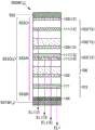


Classifications
-
- H—ELECTRICITY
- H10—SEMICONDUCTOR DEVICES; ELECTRIC SOLID-STATE DEVICES NOT OTHERWISE PROVIDED FOR
- H10K—ORGANIC ELECTRIC SOLID-STATE DEVICES
- H10K50/00—Organic light-emitting devices
- H10K50/10—OLEDs or polymer light-emitting diodes [PLED]
- H10K50/19—Tandem OLEDs
-
- H—ELECTRICITY
- H05—ELECTRIC TECHNIQUES NOT OTHERWISE PROVIDED FOR
- H05B—ELECTRIC HEATING; ELECTRIC LIGHT SOURCES NOT OTHERWISE PROVIDED FOR; CIRCUIT ARRANGEMENTS FOR ELECTRIC LIGHT SOURCES, IN GENERAL
- H05B33/00—Electroluminescent light sources
- H05B33/02—Details
-
- H—ELECTRICITY
- H05—ELECTRIC TECHNIQUES NOT OTHERWISE PROVIDED FOR
- H05B—ELECTRIC HEATING; ELECTRIC LIGHT SOURCES NOT OTHERWISE PROVIDED FOR; CIRCUIT ARRANGEMENTS FOR ELECTRIC LIGHT SOURCES, IN GENERAL
- H05B33/00—Electroluminescent light sources
- H05B33/12—Light sources with substantially two-dimensional radiating surfaces
- H05B33/14—Light sources with substantially two-dimensional radiating surfaces characterised by the chemical or physical composition or the arrangement of the electroluminescent material, or by the simultaneous addition of the electroluminescent material in or onto the light source
- H05B33/145—Arrangements of the electroluminescent material
-
- H—ELECTRICITY
- H05—ELECTRIC TECHNIQUES NOT OTHERWISE PROVIDED FOR
- H05B—ELECTRIC HEATING; ELECTRIC LIGHT SOURCES NOT OTHERWISE PROVIDED FOR; CIRCUIT ARRANGEMENTS FOR ELECTRIC LIGHT SOURCES, IN GENERAL
- H05B33/00—Electroluminescent light sources
- H05B33/12—Light sources with substantially two-dimensional radiating surfaces
- H05B33/22—Light sources with substantially two-dimensional radiating surfaces characterised by the chemical or physical composition or the arrangement of auxiliary dielectric or reflective layers
- H05B33/24—Light sources with substantially two-dimensional radiating surfaces characterised by the chemical or physical composition or the arrangement of auxiliary dielectric or reflective layers of metallic reflective layers
-
- H—ELECTRICITY
- H05—ELECTRIC TECHNIQUES NOT OTHERWISE PROVIDED FOR
- H05B—ELECTRIC HEATING; ELECTRIC LIGHT SOURCES NOT OTHERWISE PROVIDED FOR; CIRCUIT ARRANGEMENTS FOR ELECTRIC LIGHT SOURCES, IN GENERAL
- H05B33/00—Electroluminescent light sources
- H05B33/12—Light sources with substantially two-dimensional radiating surfaces
- H05B33/26—Light sources with substantially two-dimensional radiating surfaces characterised by the composition or arrangement of the conductive material used as an electrode
- H05B33/28—Light sources with substantially two-dimensional radiating surfaces characterised by the composition or arrangement of the conductive material used as an electrode of translucent electrodes
-
- H—ELECTRICITY
- H10—SEMICONDUCTOR DEVICES; ELECTRIC SOLID-STATE DEVICES NOT OTHERWISE PROVIDED FOR
- H10K—ORGANIC ELECTRIC SOLID-STATE DEVICES
- H10K50/00—Organic light-emitting devices
- H10K50/10—OLEDs or polymer light-emitting diodes [PLED]
- H10K50/11—OLEDs or polymer light-emitting diodes [PLED] characterised by the electroluminescent [EL] layers
- H10K50/125—OLEDs or polymer light-emitting diodes [PLED] characterised by the electroluminescent [EL] layers specially adapted for multicolour light emission, e.g. for emitting white light
- H10K50/13—OLEDs or polymer light-emitting diodes [PLED] characterised by the electroluminescent [EL] layers specially adapted for multicolour light emission, e.g. for emitting white light comprising stacked EL layers within one EL unit
-
- H—ELECTRICITY
- H10—SEMICONDUCTOR DEVICES; ELECTRIC SOLID-STATE DEVICES NOT OTHERWISE PROVIDED FOR
- H10K—ORGANIC ELECTRIC SOLID-STATE DEVICES
- H10K50/00—Organic light-emitting devices
- H10K50/80—Constructional details
- H10K50/805—Electrodes
- H10K50/81—Anodes
-
- H—ELECTRICITY
- H10—SEMICONDUCTOR DEVICES; ELECTRIC SOLID-STATE DEVICES NOT OTHERWISE PROVIDED FOR
- H10K—ORGANIC ELECTRIC SOLID-STATE DEVICES
- H10K50/00—Organic light-emitting devices
- H10K50/80—Constructional details
- H10K50/805—Electrodes
- H10K50/81—Anodes
- H10K50/818—Reflective anodes, e.g. ITO combined with thick metallic layers
-
- H—ELECTRICITY
- H10—SEMICONDUCTOR DEVICES; ELECTRIC SOLID-STATE DEVICES NOT OTHERWISE PROVIDED FOR
- H10K—ORGANIC ELECTRIC SOLID-STATE DEVICES
- H10K50/00—Organic light-emitting devices
- H10K50/80—Constructional details
- H10K50/805—Electrodes
- H10K50/82—Cathodes
-
- H—ELECTRICITY
- H10—SEMICONDUCTOR DEVICES; ELECTRIC SOLID-STATE DEVICES NOT OTHERWISE PROVIDED FOR
- H10K—ORGANIC ELECTRIC SOLID-STATE DEVICES
- H10K50/00—Organic light-emitting devices
- H10K50/80—Constructional details
- H10K50/805—Electrodes
- H10K50/82—Cathodes
- H10K50/826—Multilayers, e.g. opaque multilayers
-
- H—ELECTRICITY
- H10—SEMICONDUCTOR DEVICES; ELECTRIC SOLID-STATE DEVICES NOT OTHERWISE PROVIDED FOR
- H10K—ORGANIC ELECTRIC SOLID-STATE DEVICES
- H10K50/00—Organic light-emitting devices
- H10K50/80—Constructional details
- H10K50/85—Arrangements for extracting light from the devices
- H10K50/852—Arrangements for extracting light from the devices comprising a resonant cavity structure, e.g. Bragg reflector pair
-
- H—ELECTRICITY
- H10—SEMICONDUCTOR DEVICES; ELECTRIC SOLID-STATE DEVICES NOT OTHERWISE PROVIDED FOR
- H10K—ORGANIC ELECTRIC SOLID-STATE DEVICES
- H10K50/00—Organic light-emitting devices
- H10K50/80—Constructional details
- H10K50/85—Arrangements for extracting light from the devices
- H10K50/858—Arrangements for extracting light from the devices comprising refractive means, e.g. lenses
-
- H—ELECTRICITY
- H10—SEMICONDUCTOR DEVICES; ELECTRIC SOLID-STATE DEVICES NOT OTHERWISE PROVIDED FOR
- H10K—ORGANIC ELECTRIC SOLID-STATE DEVICES
- H10K59/00—Integrated devices, or assemblies of multiple devices, comprising at least one organic light-emitting element covered by group H10K50/00
- H10K59/10—OLED displays
- H10K59/12—Active-matrix OLED [AMOLED] displays
- H10K59/123—Connection of the pixel electrodes to the thin film transistors [TFT]
-
- H—ELECTRICITY
- H10—SEMICONDUCTOR DEVICES; ELECTRIC SOLID-STATE DEVICES NOT OTHERWISE PROVIDED FOR
- H10K—ORGANIC ELECTRIC SOLID-STATE DEVICES
- H10K59/00—Integrated devices, or assemblies of multiple devices, comprising at least one organic light-emitting element covered by group H10K50/00
- H10K59/10—OLED displays
- H10K59/12—Active-matrix OLED [AMOLED] displays
- H10K59/131—Interconnections, e.g. wiring lines or terminals
-
- H—ELECTRICITY
- H10—SEMICONDUCTOR DEVICES; ELECTRIC SOLID-STATE DEVICES NOT OTHERWISE PROVIDED FOR
- H10K—ORGANIC ELECTRIC SOLID-STATE DEVICES
- H10K59/00—Integrated devices, or assemblies of multiple devices, comprising at least one organic light-emitting element covered by group H10K50/00
- H10K59/30—Devices specially adapted for multicolour light emission
- H10K59/35—Devices specially adapted for multicolour light emission comprising red-green-blue [RGB] subpixels
-
- H—ELECTRICITY
- H10—SEMICONDUCTOR DEVICES; ELECTRIC SOLID-STATE DEVICES NOT OTHERWISE PROVIDED FOR
- H10K—ORGANIC ELECTRIC SOLID-STATE DEVICES
- H10K59/00—Integrated devices, or assemblies of multiple devices, comprising at least one organic light-emitting element covered by group H10K50/00
- H10K59/80—Constructional details
- H10K59/805—Electrodes
- H10K59/8051—Anodes
- H10K59/80515—Anodes characterised by their shape
-
- H—ELECTRICITY
- H10—SEMICONDUCTOR DEVICES; ELECTRIC SOLID-STATE DEVICES NOT OTHERWISE PROVIDED FOR
- H10K—ORGANIC ELECTRIC SOLID-STATE DEVICES
- H10K59/00—Integrated devices, or assemblies of multiple devices, comprising at least one organic light-emitting element covered by group H10K50/00
- H10K59/80—Constructional details
- H10K59/875—Arrangements for extracting light from the devices
-
- H—ELECTRICITY
- H10—SEMICONDUCTOR DEVICES; ELECTRIC SOLID-STATE DEVICES NOT OTHERWISE PROVIDED FOR
- H10K—ORGANIC ELECTRIC SOLID-STATE DEVICES
- H10K77/00—Constructional details of devices covered by this subclass and not covered by groups H10K10/80, H10K30/80, H10K50/80 or H10K59/80
- H10K77/10—Substrates, e.g. flexible substrates
-
- H—ELECTRICITY
- H10—SEMICONDUCTOR DEVICES; ELECTRIC SOLID-STATE DEVICES NOT OTHERWISE PROVIDED FOR
- H10K—ORGANIC ELECTRIC SOLID-STATE DEVICES
- H10K2102/00—Constructional details relating to the organic devices covered by this subclass
- H10K2102/301—Details of OLEDs
- H10K2102/302—Details of OLEDs of OLED structures
- H10K2102/3023—Direction of light emission
- H10K2102/3026—Top emission
-
- H—ELECTRICITY
- H10—SEMICONDUCTOR DEVICES; ELECTRIC SOLID-STATE DEVICES NOT OTHERWISE PROVIDED FOR
- H10K—ORGANIC ELECTRIC SOLID-STATE DEVICES
- H10K59/00—Integrated devices, or assemblies of multiple devices, comprising at least one organic light-emitting element covered by group H10K50/00
- H10K59/10—OLED displays
- H10K59/12—Active-matrix OLED [AMOLED] displays
-
- H—ELECTRICITY
- H10—SEMICONDUCTOR DEVICES; ELECTRIC SOLID-STATE DEVICES NOT OTHERWISE PROVIDED FOR
- H10K—ORGANIC ELECTRIC SOLID-STATE DEVICES
- H10K59/00—Integrated devices, or assemblies of multiple devices, comprising at least one organic light-emitting element covered by group H10K50/00
- H10K59/10—OLED displays
- H10K59/17—Passive-matrix OLED displays
Landscapes
- Physics & Mathematics (AREA)
- Optics & Photonics (AREA)
- Engineering & Computer Science (AREA)
- Microelectronics & Electronic Packaging (AREA)
- Electroluminescent Light Sources (AREA)
- Geometry (AREA)
Abstract
提供一种方便性、实用性或可靠性优异的新颖光功能器件。发光器件包括第一电极、第二电极以及EL层,第一电极具有第一透过率,第二电极与第一电极重叠,第二电极具有比第一透过率高的第二透过率。EL层夹在第一电极与第二电极间并具有第一区域、第二区域及第三区域,第一区域夹在第二区域与第三区域间,第二区域夹在第一电极与第一区域间并具有第一折射率。第三区域夹在第一区域与第二电极间并具有第二折射率,第二折射率比第一折射率低,EL层包括第一单元、第二单元及中间层,中间层夹在第一单元与第二单元间,具有向第一单元和第二单元中的一方供应空穴并向另一方供应电子的功能。

A novel optical functional device excellent in convenience, practicability or reliability is provided. The light emitting device includes a first electrode, a second electrode and an EL layer, the first electrode has a first transmittance, the second electrode overlaps with the first electrode, and the second electrode has a second transmittance higher than the first transmittance . The EL layer is sandwiched between the first electrode and the second electrode and has a first region, a second region and a third region, the first region is sandwiched between the second region and the third region, and the second region is sandwiched between the first electrode and the second region. and a region having a first refractive index. The third region is sandwiched between the first region and the second electrode and has a second refractive index, the second refractive index is lower than the first refractive index, the EL layer includes a first unit, a second unit and an intermediate layer, and the intermediate layer is sandwiched between the first and second electrodes. Between the first cell and the second cell, there is a function of supplying holes to one of the first cell and the second cell and supplying electrons to the other.
Description
技术领域technical field
本发明的一个方式涉及一种发光器件、显示面板、发光装置、显示装置、电子设备或照明装置。One aspect of the present invention relates to a light emitting device, a display panel, a light emitting device, a display device, an electronic device, or a lighting device.
注意,本发明的一个方式不局限于上述技术领域。本说明书等所公开的发明的一个方式的技术领域涉及一种物体、方法或制造方法。另外,本发明的一个方式涉及一种工序(process)、机器(machine)、产品(manufacture)或者组合物(composition of matter)。由此,更具体而言,作为本说明书所公开的本发明的一个方式的技术领域的例子可以举出半导体装置、显示装置、发光装置、蓄电装置、存储装置、这些装置的驱动方法或者这些装置的制造方法。Note that one aspect of the present invention is not limited to the technical fields described above. The technical field of one aspect of the invention disclosed in this specification etc. relates to an object, a method, or a manufacturing method. Moreover, one aspect of this invention relates to a process (process), a machine (machine), a product (manufacture), or a composition (composition of matter). Therefore, more specifically, examples of the technical field of one embodiment of the present invention disclosed in this specification include semiconductor devices, display devices, light emitting devices, power storage devices, memory devices, driving methods of these devices, or these Method of manufacturing the device.
背景技术Background technique
使用有机化合物且利用电致发光(EL:Electroluminescence)的发光器件(有机EL器件)的实用化非常活跃。在这些发光器件的基本结构中,在一对电极之间夹有含有发光材料的有机化合物层(EL层)。通过对该元件施加电压,注入载流子(空穴及电子),利用该载流子的复合能量,可以获得来自发光材料的发光。The practical use of a light-emitting device (organic EL device) using an organic compound and utilizing electroluminescence (EL: Electroluminescence) is very active. In the basic structure of these light emitting devices, an organic compound layer (EL layer) containing a light emitting material is interposed between a pair of electrodes. By applying a voltage to the element, carriers (holes and electrons) are injected, and the recombination energy of the carriers is used to obtain light emission from the light-emitting material.
因为这种发光器件是自发光型发光器件,所以当用于显示器的像素时比起液晶有可见度更高、不需要背光源等优势。因此,该发光器件适合于平板显示器元件。另外,使用这种发光器件的显示器可以被制造成薄且轻,这也是极大的优点。再者,非常高速的响应也是该发光器件的特征之一。Because this light-emitting device is a self-luminous light-emitting device, it has advantages such as higher visibility and no need for a backlight when used in pixels of a display compared to liquid crystals. Therefore, the light emitting device is suitable for flat panel display elements. In addition, a display using such a light emitting device can be made thin and light, which is also a great advantage. Furthermore, very high-speed response is also one of the characteristics of this light emitting device.
此外,因为这种发光器件的发光层可以在二维上连续地形成,所以可以获得面发光。因为这是在以白炽灯或LED为代表的点光源或者以荧光灯为代表的线光源中难以得到的特征,所以作为可应用于照明等的面光源,上述发光器件的利用价值也高。Furthermore, since the light emitting layer of this light emitting device can be continuously formed two-dimensionally, surface emission can be obtained. Since this feature is difficult to obtain in point light sources such as incandescent lamps and LEDs, or line light sources such as fluorescent lamps, the above-mentioned light-emitting devices have high utility value as surface light sources applicable to lighting and the like.
如上所述,可以将使用发光器件的显示器或照明装置适合用于各种各样的电子设备,为了追求具有更良好的特性的发光器件的研究开发日益活跃。As described above, displays and lighting devices using light-emitting devices can be suitably used in various electronic devices, and research and development for light-emitting devices with better characteristics has been actively conducted.
提取效率低是有机EL元件的常见问题之一。尤其是,因邻层间的折射率不同引起的反射导致的衰减成为元件效率下降的主要原因。为了降低该影响,提出了在EL层内部形成由低折射率材料形成的层的结构(例如,参照非专利文献1)。Low extraction efficiency is one of the common problems of organic EL elements. In particular, attenuation due to reflection due to the difference in refractive index between adjacent layers becomes a factor of lowering device efficiency. In order to reduce this influence, a structure in which a layer made of a low-refractive-index material is formed inside the EL layer has been proposed (see, for example, Non-Patent Document 1).
与具有现有结构的发光器件相比,具有该结构的发光器件可以具有更高的光提取效率及外部量子效率,但是很难在不对其他发光器件的重要特性造成不良影响的情况下将这种低折射率的层形成在EL层内部。因为,低折射率与高载流子传输性或用于发光器件时的可靠性具有权衡关系。这是因为有机化合物中的载流子传输性及可靠性大多来源于不饱和键的存在而具有很多不饱和键的有机化合物倾向于具有高折射率。Compared with light-emitting devices with existing structures, light-emitting devices with this structure can have higher light extraction efficiency and external quantum efficiency, but it is difficult to integrate such light-emitting devices without adversely affecting other important characteristics of light-emitting devices. A layer with a low refractive index is formed inside the EL layer. This is because a low refractive index has a trade-off relationship with high carrier transport properties or reliability when used in a light-emitting device. This is because carrier transport properties and reliability in organic compounds are mostly derived from the presence of unsaturated bonds, and organic compounds having many unsaturated bonds tend to have a high refractive index.
[先行技术文献][Prior Art Literature]
[专利文献][Patent Document]
[专利文献1]日本专利申请公开第平11-282181号公报[Patent Document 1] Japanese Patent Application Laid-Open No. Hei 11-282181
[专利文献2]日本专利申请公开第2009-91304号公报[Patent Document 2] Japanese Patent Application Publication No. 2009-91304
[专利文献3]美国专利申请公开第2010/104969[Patent Document 3] US Patent Application Publication No. 2010/104969
[非专利文献][Non-patent literature]
[专利文献1]Jaeho Lee等12名,“Synergetic electrode architecture forefficient graphene-based flexible organic light-emitting diodes”,natureCOMMUNICATIONS,2016年6月2日,DOI:10.1038/ncomms11791[Patent Document 1] Jaeho Lee et al. 12, "Synergetic electrode architecture efficient graphene-based flexible organic light-emitting diodes", nature COMMUNICATIONS, June 2, 2016, DOI: 10.1038/ncomms11791
发明内容Contents of the invention
发明所要解决的技术问题The technical problem to be solved by the invention
本发明的一个方式的目的之一是提供一种方便性、实用性或可靠性优异的新颖发光器件。此外,本发明的一个方式的目的之一是提供一种方便性、实用性或可靠性优异的新颖显示面板。此外,本发明的一个方式的目的之一是提供一种方便性、实用性或可靠性优异的新颖发光装置。此外,本发明的一个方式的目的之一是提供一种方便性、实用性或可靠性优异的新颖显示装置。此外,本发明的一个方式的目的之一是提供一种方便性、实用性或可靠性优异的新颖电子设备。此外,本发明的一个方式的目的之一是提供一种方便性、实用性或可靠性优异的新颖照明装置。另外,本发明的一个方式的目的之一是提供一种新颖发光器件、新颖显示面板、新颖发光装置、新颖显示装置、新颖电子设备或新颖照明装置。One of the objects of one aspect of the present invention is to provide a novel light-emitting device excellent in convenience, practicality, or reliability. Another object of one aspect of the present invention is to provide a novel display panel excellent in convenience, practicality, or reliability. Another object of one aspect of the present invention is to provide a novel light-emitting device excellent in convenience, practicality, or reliability. Another object of one aspect of the present invention is to provide a novel display device excellent in convenience, utility, or reliability. Another object of one aspect of the present invention is to provide a novel electronic device excellent in convenience, utility, or reliability. Another object of one aspect of the present invention is to provide a novel lighting device excellent in convenience, practicality, or reliability. Another object of one aspect of the present invention is to provide a novel light emitting device, a novel display panel, a novel light emitting device, a novel display device, a novel electronic device, or a novel lighting device.
注意,这些目的的记载不妨碍其他目的的存在。注意,本发明的一个方式并不需要实现所有上述目的。另外,从说明书、附图、权利要求书等的记载中可明显看出上述目的以外的目的,可以从说明书、附图、权利要求书等的记载中抽出上述目的以外的目的。Note that the description of these purposes does not prevent the existence of other purposes. Note that one aspect of the present invention does not necessarily achieve all of the above objects. In addition, objects other than the above-mentioned objects are apparent from the descriptions of the specification, drawings, claims, etc., and objects other than the above-mentioned objects can be extracted from the descriptions of the specification, drawings, and claims.
解决技术问题的手段means of solving technical problems
(1)本发明的一个方式包括第一电极、第二电极以及EL层。(1) One aspect of the present invention includes a first electrode, a second electrode, and an EL layer.
第一电极具有第一透过率T1。第二电极具有与第一电极重叠的区域,第二电极具有第二透过率T2。第二透过率T2比第一透过率T1高。The first electrode has a first transmittance T1. The second electrode has a region overlapping with the first electrode, and the second electrode has a second transmittance T2. The second transmittance T2 is higher than the first transmittance T1.
EL层具有夹在第一电极与第二电极间的区域,EL层具有第一区域、第二区域及第三区域,第一区域具有夹在第二区域与第三区域间的部分。The EL layer has a region sandwiched between the first electrode and the second electrode, the EL layer has a first region, a second region, and a third region, and the first region has a portion sandwiched between the second region and the third region.
第二区域具有夹在第一电极与第一区域间的区域,第二区域具有第一折射率n1。The second region has a region sandwiched between the first electrode and the first region, and the second region has a first refractive index n1.
第三区域具有夹在第一区域与第二电极间的区域,第三区域具有第二折射率n2,第二折射率n2比第一折射率n1低。The third region has a region sandwiched between the first region and the second electrode, and the third region has a second refractive index n2 which is lower than the first refractive index n1.
EL层包括第一单元、第二单元及中间层,中间层夹在第一单元与第二单元间。The EL layer includes a first unit, a second unit and an intermediate layer, and the intermediate layer is sandwiched between the first unit and the second unit.
中间层具有向第一单元和第二单元中的一方供应空穴并向另一方供应电子的功能。The intermediate layer has a function of supplying holes to one of the first unit and the second unit and supplying electrons to the other.
第一单元夹在第一电极与中间层间,并包括第一含有发光材料的层。The first unit is sandwiched between the first electrode and the intermediate layer, and includes a first layer containing a luminescent material.
第二单元夹在中间层与第二电极间,并包括第二含有发光材料的层。The second unit is sandwiched between the intermediate layer and the second electrode, and includes a second layer containing a light emitting material.
第一区域包括第一含有发光材料的层及第二含有发光材料的层。The first region includes a first layer containing a luminescent material and a second layer containing a luminescent material.
由此,可以从第二电极高效地提取从第一区域发射的光。此外,能够在将电流密度保持为低的同时以高亮度进行发光。另外,可以提高可靠性。此外,可以降低在以同一亮度进行比较时的驱动电压。此外,可以抑制功耗。其结果,可以提供一种方便性、实用性或可靠性优异的新颖光功能器件。Thereby, light emitted from the first region can be efficiently extracted from the second electrode. In addition, it is possible to emit light with high luminance while keeping the current density low. In addition, reliability can be improved. In addition, it is possible to reduce the driving voltage when comparing at the same luminance. In addition, power consumption can be suppressed. As a result, a novel optical functional device excellent in convenience, practicality, or reliability can be provided.
(2)另外,本发明的一个方式是上述发光器件,其中第一含有发光材料的层具有发射蓝色光的功能,第二含有发光材料的层也具有发射蓝色光的功能。(2) In addition, one aspect of the present invention is the above-mentioned light-emitting device, wherein the first layer containing a light-emitting material has a function of emitting blue light, and the second layer containing a light-emitting material also has a function of emitting blue light.
由此,可以在含有发光材料的层所发射的光和含有发光材料的层所发射的光彼此增强的位置配置上述层。另外,可以在含有发光材料的层所发射的光和被电极反射的光彼此增强的位置配置含有发光材料的层。另外,可以从第二电极高效地提取从第一区域发射的光。其结果,可以提供一种方便性、实用性或可靠性优异的新颖光功能器件。Accordingly, the layer can be arranged at a position where the light emitted from the layer containing the luminescent material and the light emitted from the layer containing the luminescent material are mutually intensified. In addition, the layer containing the luminescent material may be disposed at a position where light emitted from the layer containing the luminescent material and light reflected by the electrodes are mutually intensified. In addition, light emitted from the first region can be efficiently extracted from the second electrode. As a result, a novel optical functional device excellent in convenience, practicality, or reliability can be provided.
(3)另外,本发明的一个方式是上述发光器件,其中第二单元包括第三含有发光材料的层。(3) In addition, one aspect of the present invention is the above-mentioned light-emitting device, wherein the second unit includes a third layer containing a light-emitting material.
第一含有发光材料的层具有发射蓝色光的功能,第二含有发光材料的层具有发射红色光的功能,第三含有发光材料的层具有发射绿色光的功能。The first layer containing luminescent material has the function of emitting blue light, the second layer containing luminescent material has the function of emitting red light, and the third layer containing luminescent material has the function of emitting green light.
由此,可以从第一区域发射多个颜色的光。另外,可以在含有发光材料的层所发射的光和被第一电极反射的光彼此增强的位置配置含有发光材料的层。另外,可以根据含有发光材料的层所发射的光的波长配置含有发光材料的层。另外,可以提供显色性优良的发光器件。另外,可以从第二电极高效地提取从第一区域发射的光。其结果,可以提供一种方便性、实用性或可靠性优异的新颖光功能器件。Thereby, light of a plurality of colors can be emitted from the first region. In addition, the layer containing the light emitting material may be arranged at a position where the light emitted from the layer containing the light emitting material and the light reflected by the first electrode reinforce each other. In addition, the layer containing the light emitting material may be configured according to the wavelength of light emitted by the layer containing the light emitting material. In addition, a light emitting device excellent in color rendering can be provided. In addition, light emitted from the first region can be efficiently extracted from the second electrode. As a result, a novel optical functional device excellent in convenience, practicality, or reliability can be provided.
(4)另外,本发明的一个方式是上述发光器件,其中第三区域的电子传输性比第二区域高。(4) In addition, one aspect of the present invention is the above-mentioned light-emitting device, wherein the electron transport property of the third region is higher than that of the second region.
(5)另外,本发明的一个方式是上述发光器件,其中第三区域的空穴传输性比第二区域高。(5) In addition, one aspect of the present invention is the above light-emitting device, wherein the third region has higher hole transport properties than the second region.
(6)另外,本发明的一个方式是一种显示面板,包括功能层以及像素。(6) In addition, one aspect of the present invention is a display panel including a functional layer and pixels.
功能层包括像素电路,像素包括像素电路及上述发光器件。另外,第一电极具有夹在功能层与第二电极间的区域,第一电极与像素电路电连接。The functional layer includes a pixel circuit, and the pixel includes the pixel circuit and the above-mentioned light emitting device. In addition, the first electrode has a region sandwiched between the functional layer and the second electrode, and the first electrode is electrically connected to the pixel circuit.
由此,可以使用像素电路控制发光器件的发光。另外,可以显示图像信息。其结果,可以提供一种方便性、实用性或可靠性优异的新颖光功能器件。Thereby, the light emission of the light emitting device can be controlled using the pixel circuit. In addition, image information can be displayed. As a result, a novel optical functional device excellent in convenience, practicality, or reliability can be provided.
(7)另外,本发明的一个方式是一种发光装置,包括上述发光器件、以及晶体管或衬底。(7) Another aspect of the present invention is a light-emitting device including the above-mentioned light-emitting device, and a transistor or a substrate.
(8)另外,本发明的一个方式是一种显示装置,包括上述发光器件、以及晶体管或衬底。(8) Another aspect of the present invention is a display device including the above-mentioned light emitting device, and a transistor or a substrate.
(9)另外,本发明的一个方式是一种照明装置,包括上述发光装置及框体。(9) Moreover, one aspect of the present invention is a lighting device including the above-mentioned light-emitting device and a housing.
(10)另外,本发明的一个方式是一种电子设备,包括上述显示装置、以及传感器、操作按钮、扬声器或麦克风。(10) Another aspect of the present invention is an electronic device including the display device described above, a sensor, an operation button, a speaker, or a microphone.
在本说明书的附图中,根据其功能对构成要素进行分类而示出为彼此独立的方框的方框图,但是,实际上的构成要素难以根据其功能完全划分,而一个构成要素会涉及多个功能。In the drawings of this specification, the constituent elements are classified according to their functions and shown as block diagrams of mutually independent blocks. However, it is difficult to completely divide the actual constituent elements according to their functions, and one constituent element involves multiple Function.
另外,本说明书中的发光装置包括使用发光元件的图像显示器件。另外,发光装置有时还包括如下模块:发光元件安装有连接器诸如各向异性导电膜或TCP(Tape CarrierPackage:带载封装)的模块;在TCP的端部设置有印刷线路板的模块;通过COG(Chip OnGlass:玻璃覆晶封装)方式在发光元件上直接安装有IC(集成电路)的模块。而且,照明装置等有时包括发光装置。In addition, the light emitting device in this specification includes an image display device using a light emitting element. In addition, the light-emitting device sometimes also includes the following modules: a module in which a connector such as an anisotropic conductive film or TCP (Tape Carrier Package: Tape Carrier Package) is mounted on a light-emitting element; a module in which a printed wiring board is provided at the end of the TCP; (Chip On Glass: chip-on-glass packaging) is a module in which an IC (integrated circuit) is directly mounted on a light-emitting element. Also, lighting devices and the like sometimes include light emitting devices.
发明效果Invention effect
根据本发明的一个方式,可以提供一种方便性、实用性或可靠性优异的新颖发光器件。此外,根据本发明的一个方式,可以提供一种方便性、实用性或可靠性优异的新颖显示面板。此外,根据本发明的一个方式,可以提供一种方便性、实用性或可靠性优异的新颖发光装置。此外,根据本发明的一个方式,可以提供一种方便性、实用性或可靠性优异的新颖显示装置。此外,根据本发明的一个方式,可以提供一种方便性、实用性或可靠性优异的新颖电子设备。此外,根据本发明的一个方式,可以提供一种方便性、实用性或可靠性优异的新颖照明装置。另外,根据本发明的一个方式,可以提供一种新颖发光器件、新颖显示面板、新颖发光装置、新颖显示装置、新颖电子设备或新颖照明装置。According to one aspect of the present invention, it is possible to provide a novel light-emitting device excellent in convenience, practicality, or reliability. Furthermore, according to one aspect of the present invention, a novel display panel excellent in convenience, practicality, or reliability can be provided. Furthermore, according to one aspect of the present invention, it is possible to provide a novel light-emitting device excellent in convenience, practicality, or reliability. Furthermore, according to one aspect of the present invention, it is possible to provide a novel display device excellent in convenience, utility, or reliability. Furthermore, according to one aspect of the present invention, it is possible to provide a novel electronic device excellent in convenience, utility, or reliability. Furthermore, according to one aspect of the present invention, it is possible to provide a novel lighting device excellent in convenience, practicality, or reliability. In addition, according to one aspect of the present invention, a novel light-emitting device, a novel display panel, a novel light-emitting device, a novel display device, a novel electronic device, or a novel lighting device can be provided.
注意,这些效果的记载不妨碍其他效果的存在。注意,本发明的一个方式并不需要具有所有上述效果。另外,从说明书、附图、权利要求书等的记载中可明显看出上述效果以外的效果,可以从说明书、附图、权利要求书等的记载中抽出上述效果以外的效果。Note that the description of these effects does not prevent the existence of other effects. Note that one aspect of the present invention does not necessarily have all the above effects. In addition, effects other than the above-mentioned effects are apparent from the descriptions of the specification, drawings, and claims, and effects other than the above-mentioned effects can be extracted from the descriptions of the specification, drawings, and claims.
附图简要说明Brief description of the drawings
图1A及图1B是说明根据实施方式的发光器件的结构的图。1A and 1B are diagrams illustrating a structure of a light emitting device according to an embodiment.
图2A及图2B是说明根据实施方式的发光器件的结构的图。2A and 2B are diagrams illustrating a structure of a light emitting device according to an embodiment.
图3A及图3B是说明根据实施方式的发光器件的结构的图。3A and 3B are diagrams illustrating a structure of a light emitting device according to an embodiment.
图4A及图4B是说明根据实施方式的发光器件的结构的图。4A and 4B are diagrams illustrating a structure of a light emitting device according to an embodiment.
图5A及图5B是说明根据实施方式的发光器件的结构的图。5A and 5B are diagrams illustrating a structure of a light emitting device according to an embodiment.
图6A及图6B是说明根据实施方式的功能面板的结构的图。6A and 6B are diagrams illustrating the structure of the function panel according to the embodiment.
图7A至图7C是说明根据实施方式的功能面板的结构的图。7A to 7C are diagrams illustrating a structure of a function panel according to an embodiment.
图8是说明根据实施方式的功能面板的结构的电路图。FIG. 8 is a circuit diagram illustrating a structure of a function panel according to an embodiment.
图9是说明根据实施方式的功能面板的结构的截面图。FIG. 9 is a cross-sectional view illustrating a structure of a function panel according to an embodiment.
图10A及图10B是说明根据实施方式的功能面板的结构的截面图。10A and 10B are cross-sectional views illustrating the structure of the functional panel according to the embodiment.
图11A及图11B是说明根据实施方式的功能面板的结构的截面图。11A and 11B are cross-sectional views illustrating the structure of a functional panel according to an embodiment.
图12A及图12B是说明根据实施方式的功能面板的结构的截面图。12A and 12B are cross-sectional views illustrating the structure of the functional panel according to the embodiment.
图13A及图13B是有源矩阵型发光装置的概念图。13A and 13B are conceptual diagrams of an active matrix light emitting device.
图14A及图14B是有源矩阵型发光装置的概念图。14A and 14B are conceptual diagrams of an active matrix light emitting device.
图15是有源矩阵型发光装置的概念图。Fig. 15 is a conceptual diagram of an active matrix light emitting device.
图16A及图16B是无源矩阵型发光装置的概念图。16A and 16B are conceptual diagrams of a passive matrix light emitting device.
图17A及图17B是示出照明装置的图。17A and 17B are diagrams illustrating lighting devices.
图18A、图18B1、图18B2及图18C是示出电子设备的图。18A , 18B1 , 18B2 , and 18C are diagrams showing electronic devices.
图19A至图19C是示出电子设备的图。19A to 19C are diagrams illustrating electronic devices.
图20是示出照明装置的图。Fig. 20 is a diagram illustrating a lighting device.
图21是示出照明装置的图。Fig. 21 is a diagram illustrating a lighting device.
图22是示出车载显示装置及照明装置的图。FIG. 22 is a diagram showing an on-vehicle display device and a lighting device.
图23A至图23C是示出电子设备的图。23A to 23C are diagrams illustrating electronic devices.
图24是说明根据实施例的发光器件的结构的图。FIG. 24 is a diagram illustrating a structure of a light emitting device according to an embodiment.
图25是说明用于发光器件1至发光器件3的材料的波长-寻常光折射率特性的图。FIG. 25 is a graph illustrating wavelength-ordinary light refractive index characteristics of materials used in the light-emitting
图26是说明根据实施例的发光器件的结构的发射光谱。FIG. 26 is an emission spectrum illustrating the structure of the light emitting device according to the embodiment.
实施发明的方式Ways of Carrying Out the Invention
发光器件包括第一电极、第二电极以及EL层,第一电极具有第一透过率,第二电极具有与第一电极重叠的区域,第二电极具有第二透过率,第二透过率比第一透过率高。EL层具有夹在第一电极与第二电极间的区域,EL层具有第一区域、第二区域及第三区域,第一区域具有夹在第二区域与第三区域间的部分,第二区域具有夹在第一电极与第一区域间的区域,第二区域具有第一折射率,第三区域具有夹在第一区域与第二电极间的区域,第三区域具有第二折射率,第二折射率比第一折射率低。另外,EL层包括第一单元、第二单元及中间层,中间层夹在第一单元与第二单元间,中间层具有向第一单元和第二单元中的一方供应空穴并向另一方供应电子的功能,第一单元夹在第一电极与中间层间,第一单元包括第一含有发光材料的层,第二单元夹在中间层与第二电极间,第二单元包括第二含有发光材料的层。第一区域包括第一含有发光材料的层及第二含有发光材料的层。The light emitting device includes a first electrode, a second electrode and an EL layer, the first electrode has a first transmittance, the second electrode has a region overlapping with the first electrode, the second electrode has a second transmittance, and the second transmittance The ratio is higher than the first transmittance. The EL layer has a region sandwiched between the first electrode and the second electrode, the EL layer has a first region, a second region, and a third region, the first region has a portion sandwiched between the second region and the third region, and the second region has a portion sandwiched between the second region and the third region. the region has a region sandwiched between the first electrode and the first region, the second region has a first refractive index, the third region has a region sandwiched between the first region and the second electrode, the third region has a second refractive index, The second refractive index is lower than the first refractive index. In addition, the EL layer includes a first unit, a second unit and an intermediate layer, the intermediate layer is sandwiched between the first unit and the second unit, and the intermediate layer has a function of supplying holes to one of the first unit and the second unit and supplying holes to the other The function of supplying electrons, the first unit is sandwiched between the first electrode and the middle layer, the first unit includes the first layer containing the luminescent material, the second unit is sandwiched between the middle layer and the second electrode, the second unit includes the second layer containing A layer of emissive material. The first region includes a first layer containing a luminescent material and a second layer containing a luminescent material.
由此,可以从第二电极高效地提取从第一区域发射的光。此外,能够在将电流密度保持为低的同时以高亮度进行发光。另外,可以提高可靠性。此外,可以降低在以同一亮度进行比较时的驱动电压。此外,可以抑制功耗。其结果,可以提供一种方便性、实用性或可靠性优异的新颖光功能器件。Thereby, light emitted from the first region can be efficiently extracted from the second electrode. In addition, it is possible to emit light with high luminance while keeping the current density low. In addition, reliability can be improved. In addition, it is possible to reduce the driving voltage when comparing at the same luminance. In addition, power consumption can be suppressed. As a result, a novel optical functional device excellent in convenience, practicality, or reliability can be provided.
参照附图对实施方式进行详细说明。注意,本发明不局限于以下说明,而所属技术领域的普通技术人员可以很容易地理解一个事实就是其方式及详细内容在不脱离本发明的宗旨及其范围的情况下可以被变换为各种各样的形式。因此,本发明不应该被解释为仅限定在以下所示的实施方式所记载的内容中。注意,在下面说明的发明结构中,在不同的附图中共同使用相同的符号来表示相同的部分或具有相同功能的部分,而省略反复说明。Embodiments are described in detail with reference to the drawings. Note that the present invention is not limited to the following descriptions, and those skilled in the art can easily understand the fact that the manner and details can be changed into various forms without departing from the spirit and scope of the present invention. in various forms. Therefore, the present invention should not be interpreted as being limited only to the contents described in the embodiments shown below. Note that in the configuration of the invention described below, the same symbols are commonly used in different drawings to denote the same parts or parts having the same functions, and repeated descriptions are omitted.
(实施方式1)(Embodiment 1)
在本实施方式中,参照图1至图3说明本发明的一个方式的发光器件150的结构。In this embodiment mode, the structure of a
图1A是说明本发明的一个方式的发光器件的结构的图,图1B是说明与图1A不同的本发明的一个方式的发光器件的结构的图。FIG. 1A is a diagram illustrating a configuration of a light emitting device according to one embodiment of the present invention, and FIG. 1B is a diagram illustrating a configuration of a light emitting device according to one embodiment of the present invention different from FIG. 1A .
图2A是说明本发明的一个方式的发光器件的结构的图,图2B是说明与图2A不同的本发明的一个方式的发光器件的结构的图。FIG. 2A is a diagram illustrating a structure of a light emitting device according to one embodiment of the present invention, and FIG. 2B is a diagram illustrating a structure of a light emitting device according to one embodiment of the present invention different from FIG. 2A .
图3A是说明本发明的一个方式的发光器件的结构的截面图,图3B是说明与图3A不同的本发明的一个方式的发光器件的结构的截面图。3A is a cross-sectional view illustrating a structure of a light emitting device according to one embodiment of the present invention, and FIG. 3B is a cross-sectional view illustrating a structure of a light emitting device according to one embodiment of the present invention different from FIG. 3A .
<发光器件150的结构例子1><Structural Example 1 of Light-Emitting
本实施方式中说明的发光器件150包括电极551(i,j)、电极552及EL层553(参照图1A)。The light-emitting
电极551(i,j)具有透过率T1。另外,电极552具有与电极551(i,j)重叠的区域,并具有透过率T2。透过率T2比透过率T1高。另外,电极551(i,j)具有比电极552高的反射率。The electrode 551(i,j) has a transmittance T1. In addition, the
<EL层553的结构例子1><Structural Example 1 of
EL层553具有夹在电极551(i,j)与电极552间的区域。另外,EL层553具有区域553A、区域553B及区域553C。The
区域553A具有夹在区域553B与区域553C间的部分。另外,区域553A包括含有发光材料的层111及层111(12)。The
区域553B具有夹在电极551(i,j)与区域553A间的区域,并具有折射率n1。The
区域553C具有夹在区域553A与电极552间的区域,并具有折射率n2。折射率n2比折射率n1低。The
<EL层553的结构例子2><Structural Example 2 of
EL层553包括单元103、单元103(12)及中间层106(参照图1A)。The
<<中间层106的结构例子>><<Structural Example of
中间层106夹在单元103与单元103(12)间,中间层106具有向单元103和单元103(12)中的一方供应空穴并向另一方供应电子的功能。The
<<单元103的结构例子1>><<Structure Example 1 of
单元103夹在电极551(i,j)与中间层106间,并包括含有发光材料的层111。
<<单元103(12)的结构例子1>><<Structure Example 1 of Unit 103(12)>>
单元103(12)夹在中间层106与电极552间,并包括含有发光材料的层111(12)。Cell 103(12) is sandwiched between
<<区域553A的结构例子>><<Structure example of
区域553A包括含有发光材料的层111及含有发光材料的层111(12)。例如,含有发光材料的层111(12)具有夹在含有发光材料的层111与电极552间的区域。
由此,可以从电极552高效地提取从区域553A发射的光。此外,能够在将电流密度保持为低的同时以高亮度进行发光。另外,可以提高可靠性。此外,可以降低在以同一亮度进行比较时的驱动电压。此外,可以抑制功耗。其结果,可以提供一种方便性、实用性或可靠性优异的新颖光功能器件。Thereby, the light emitted from the
<<单元103(12)的结构例子2>><<Structure Example 2 of Unit 103(12)>>
例如,可以将发射与单元103所发射的光相同的颜色的光的结构用于单元103(12)。具体而言,可以将发射蓝色光的发光材料用于含有发光材料的层111及含有发光材料的层111(12)。For example, a structure that emits light of the same color as that emitted by the
由此,可以在含有发光材料的层111所发射的光和含有发光材料的层111(12)所发射的光彼此增强的位置配置上述层。另外,可以在含有发光材料的层所发射的光和被电极551(i,j)反射的光彼此增强的位置配置含有发光材料的层。另外,可以从电极552高效地提取从区域553A发射的光。其结果,可以提供一种方便性、实用性或可靠性优异的新颖光功能器件。Accordingly, the layers can be arranged at positions where the light emitted from the
<<单元103(12)的结构例子3>><<Structure Example 3 of Unit 103(12)>>
单元103(12)包括含有发光材料的层111(13)(参照图2A)。例如,含有发光材料的层111(12)具有夹在含有发光材料的层111与电极552间的区域,含有发光材料的层111(13)具有夹在含有发光材料的层111(12)与电极552间的区域。The cell 103(12) comprises a layer 111(13) comprising a luminescent material (cf. FIG. 2A). For example, the layer 111 (12) containing the luminescent material has a region sandwiched between the layer 111 (12) containing the luminescent material and the
<<含有发光材料的层的结构例子1>><<Structural Example 1 of Layer Containing Luminescent Material>>
含有发光材料的层111具有发射蓝色光的功能,含有发光材料的层111(12)具有发射红色光的功能,含有发光材料的层111(13)具有发射绿色光的功能。例如,含有发光材料的层111(12)具有夹在含有发光材料的层111与电极552间的区域,含有发光材料的层111(13)具有夹在含有发光材料的层111与含有发光材料的层111(12)间的区域。The
由此,可以从区域553A发射多个颜色的光。另外,可以在含有发光材料的层所发射的光和被电极551(i,j)反射的光彼此增强的位置配置含有发光材料的层。另外,可以根据含有发光材料的层所发射的光的波长配置含有发光材料的层。另外,可以提供显色性优良的发光器件。另外,可以从电极552高效地提取从区域553A发射的光。其结果,可以提供一种方便性、实用性或可靠性优异的新颖光功能器件。Thereby, light of a plurality of colors can be emitted from the
<发光器件150的结构例子2><Structural Example 2 of
另外,本实施方式中说明的发光器件150包括电极551(i,j)、电极552及EL层553(参照图1B)。In addition, the
注意,发光器件150的结构例子2与参照图1A说明的发光器件的不同之处在于:电极552的透过率T2比电极551(i,j)的透过率T1低;以及区域553B的折射率n1比区域553C的折射率n2低。在此,对不同之处进行详细说明,而关于能够使用与上述结构相同的结构的部分援用上述说明。Note that the structural example 2 of the
由此,可以从电极551(i,j)高效地提取从区域553A发射的光。此外,能够在将电流密度保持为低的同时以高亮度进行发光。另外,可以提高可靠性。此外,可以降低在以同一亮度进行比较时的驱动电压。此外,可以抑制功耗。其结果,可以提供一种方便性、实用性或可靠性优异的新颖光功能器件。Thereby, the light emitted from the
<<单元103(12)的结构例子4>><<Structure Example 4 of Unit 103(12)>>
例如,可以将发射与单元103所发射的光相同的颜色的光的结构用于单元103(12)。具体而言,可以将发射蓝色光的发光材料用于含有发光材料的层111及含有发光材料的层111(12)。For example, a structure that emits light of the same color as that emitted by the
由此,可以在含有发光材料的层111所发射的光和含有发光材料的层111(12)所发射的光彼此增强的位置配置上述层。另外,可以在含有发光材料的层所发射的光和被电极552反射的光彼此增强的位置配置含有发光材料的层。另外,可以从电极551(i,j)高效地提取区域553A所发射的光。其结果,可以提供一种方便性、实用性或可靠性优异的新颖光功能器件。Accordingly, the layers can be arranged at positions where the light emitted from the
<<单元103的结构例子2>><<Structure Example 2 of
单元103包括含有发光材料的层111(13)(参照图2B)。例如,含有发光材料的层111(12)具有夹在含有发光材料的层111与电极552间的区域,含有发光材料的层111(13)具有夹在含有发光材料的层111与电极551(i,j)间的区域。The
<<含有发光材料的层的结构例子2>><<Structural Example 2 of Layer Containing Luminescent Material>>
含有发光材料的层111具有发射红色光的功能,含有发光材料的层111(12)具有发射蓝色光的功能,含有发光材料的层111(13)具有发射绿色光的功能。The
由此,可以从区域553A发射多个颜色的光。另外,可以在含有发光材料的层所发射的光和被电极552反射的光彼此增强的位置配置含有发光材料的层。另外,可以根据含有发光材料的层所发射的光的波长配置含有发光材料的层。另外,可以提供显色性优良的发光器件。另外,可以从电极551(i,j)高效地提取从区域553A发射的光。其结果,可以提供一种方便性、实用性或可靠性优异的新颖光功能器件。Thereby, light of a plurality of colors can be emitted from the
<发光器件150的结构例子3><Structural Example 3 of Light-Emitting
本实施方式中说明的发光器件150包括电极101、电极102及EL层553(参照图3A)。电极102具有与电极101重叠的区域。The
EL层553具有夹在电极101与电极102间的区域。另外,EL层553具有区域553A、区域553B及区域553C。区域553A具有夹在区域553B与区域553C间的部分。The
<发光器件150的结构例子4><Structural Example 4 of Light-Emitting
另外,本实施方式中说明的发光器件150包括电极101、电极102及EL层553(参照图3B)。该发光器件150与参照图3A说明的发光器件的不同之处在于:区域553C包括中间层106;以及中间层106与电极102接触。In addition, the light-emitting
注意,本实施方式可以与本说明书所示的其他实施方式适当地组合。Note that this embodiment mode can be appropriately combined with other embodiment modes shown in this specification.
(实施方式2)(Embodiment 2)
在本实施方式中,参照图4及图5说明本发明的一个方式的发光器件150的结构。In this embodiment mode, the configuration of a
图4A是说明本发明的一个方式的发光器件的结构的图,图4B是说明与图4A不同的本发明的一个方式的发光器件的结构的图。FIG. 4A is a diagram illustrating a structure of a light emitting device according to one embodiment of the present invention, and FIG. 4B is a diagram illustrating a structure of a light emitting device according to one embodiment of the present invention different from FIG. 4A .
图5A是说明本发明的一个方式的发光器件的结构的图,图5B是说明与图5A不同的本发明的一个方式的发光器件的结构的图。FIG. 5A is a diagram illustrating a structure of a light emitting device according to one embodiment of the present invention, and FIG. 5B is a diagram illustrating a structure of a light emitting device according to one embodiment of the present invention which is different from FIG. 5A .
<发光器件150的结构例子1><Structural Example 1 of Light-Emitting
本实施方式中说明的发光器件150包括电极551(i,j)、电极552及EL层553(参照图4A)。The
电极551(i,j)具有透过率T1。电极552具有与电极551(i,j)重叠的区域,电极552具有透过率T2。另外,透过率T2比透过率T1高。另外,电极551(i,j)具有比电极552高的反射率。The electrode 551(i,j) has a transmittance T1. The
可以将电极551(i,j)和电极552中的任一方用作阳极且将另一方用作阴极。Either one of the electrode 551(i,j) and the
例如,可以将具有4.0eV以上的功函数的材料适合用于阳极。For example, a material having a work function of 4.0 eV or higher can be suitably used for the anode.
例如,可以将功函数比阳极小的材料用于阴极。具体而言,可以适合使用具有3.8eV以下的功函数的材料。For example, a material with a smaller work function than the anode can be used for the cathode. Specifically, a material having a work function of 3.8 eV or less can be suitably used.
例如,可以将属于元素周期表中的第1族的元素、属于元素周期表中的第2族的元素、稀土金属及包含它们的合金用于阴极。For example, elements belonging to
具体而言,可以将锂(Li)、铯(Cs)等、镁(Mg)、钙(Ca)、锶(Sr)等、铕(Eu)、镱(Yb)等及包含它们的合金(MgAg、AlLi)用于阴极。Specifically, lithium (Li), cesium (Cs) and the like, magnesium (Mg), calcium (Ca), strontium (Sr) and the like, europium (Eu), ytterbium (Yb) and the like, and alloys containing them (MgAg , AlLi) for the cathode.
<<电极551(i,j)的结构例子1>><<Structure Example 1 of Electrode 551(i,j)>>
例如,可以将导电材料用于电极551(i,j)。或者,可以将层叠反射膜和导电膜的材料用于电极551(i,j)。For example, a conductive material may be used for the electrodes 551(i,j). Alternatively, a material that laminates a reflective film and a conductive film may be used for the electrodes 551(i, j).
具体而言,可以使用金属、合金、导电化合物及它们的混合物等。Specifically, metals, alloys, conductive compounds, mixtures thereof, and the like can be used.
例如,可以使用氧化铟-氧化锡(ITO:Indium Tin Oxide,铟锡氧化物)、包含硅或氧化硅的氧化铟-氧化锡、氧化铟-氧化锌、包含氧化钨及氧化锌的氧化铟(IWZO)等。For example, indium oxide-tin oxide (ITO: Indium Tin Oxide, indium tin oxide), indium oxide-tin oxide containing silicon or silicon oxide, indium oxide-zinc oxide, indium oxide containing tungsten oxide and zinc oxide ( IWZO) and so on.
例如,可以使用金(Au)、铂(Pt)、镍(Ni)、钨(W)、铬(Cr)、钼(Mo)、铁(Fe)、钴(Co)、铜(Cu)、钯(Pd)或金属材料的氮化物(例如,氮化钛)等。此外,可以使用石墨烯。For example, gold (Au), platinum (Pt), nickel (Ni), tungsten (W), chromium (Cr), molybdenum (Mo), iron (Fe), cobalt (Co), copper (Cu), palladium (Pd) or a nitride of a metal material (for example, titanium nitride), or the like. In addition, graphene can be used.
<<电极552的结构例子1>><<Structural Example 1 of
可以将金属、合金、导电化合物以及它们的混合物等用于电极552。Metals, alloys, conductive compounds, mixtures thereof, and the like can be used for the
<<EL层553的结构例子1>><<Structure Example 1 of
EL层553具有夹在电极551(i,j)与电极552间的区域(参照图4A)。另外,EL层553具有区域553A、区域553B及区域553C。另外,区域553A具有夹在区域553B与区域553C间的部分。The
另外,EL层553包括单元103、单元103(12)、层104、层105、层105(12)及中间层106。单元103包括层111、层112及层113。单元103(12)包括层111(12)、层111(13)、层112(12)及层113(12)。中间层106包括层106A及层106B。In addition, the
<<区域553C的结构例子1>><<Structure Example 1 of
可以将其折射率n2低于区域553B的折射率n1且其电子传输性高于区域553B的电子传输性的材料用于区域553C(参照图4A)。通过降低区域553C的折射率n2,可以提高发光器件150的光提取效率。另外,折射率n2与折射率n1之差优选为0.05以上,更优选为0.1以上,进一步优选为0.15以上。另外,区域553C包括层113(12)及层105(12)。A material whose refractive index n2 is lower than the refractive index n1 of the
在本实施方式中说明的发光器件150中,可以将电极551(i,j)用作阳极并将电极552用作阴极。另外,中间层106可以向单元103供应电子并向单元103(12)供应空穴。In the
例如,可以将如下材料用于区域553C,即蓝色发光区域(455nm以上且465nm以下)的寻常光折射率为1.50以上且1.75以下或者通常用于折射率的测定的633nm的光的寻常光折射率为1.45以上且1.70以下的具有电子传输性的材料。For example, for the
注意,在材料具有各向异性时,有时寻常光折射率与异常光折射率不同。在所测量的薄膜处于上述状态时,可以通过进行各向异性分析分别算出寻常光折射率与异常光折射率。注意,在本说明书中,在所测量的材料具有寻常光折射率及异常光折射率的双方时,使用寻常光折射率作为指标。Note that when the material has anisotropy, the ordinary light refractive index may differ from the extraordinary light refractive index. When the film to be measured is in the above state, the ordinary light refractive index and the extraordinary light refractive index can be respectively calculated by performing anisotropy analysis. Note that in this specification, when the material to be measured has both the ordinary refractive index and the extraordinary refractive index, the ordinary refractive index is used as an index.
[具有电子传输性的材料][Materials with electron transport properties]
作为构成上述具有电子传输性的材料的一个例子,可以举出具有至少一个氮原子数为1至3的六元环杂芳环,包括多个成环碳原子数为6至14的芳香烃环,多个上述芳香烃环中的至少两个是苯环,并包含多个以sp3杂化轨道形成键合的烃基的有机化合物。As an example of the above-mentioned electron-transporting material, there can be mentioned a six-membered heteroaromatic ring with at least one nitrogen atom number of 1 to 3, including a plurality of aromatic hydrocarbon rings with 6 to 14 ring carbon atoms. , an organic compound in which at least two of the above-mentioned aromatic hydrocarbon rings are benzene rings and contain a plurality of hydrocarbon groups bonded by sp3 hybrid orbitals.
另外,在这种有机化合物中,分子的总碳原子数中以sp3杂化轨道形成键合的碳原子数之比例优选占10%以上且60%以下,更优选占10%以上且50%以下。或者,在这种有机化合物中,在利用1H-NMR对该有机化合物进行测量的结果中小于4ppm的信号的积分值优选为4ppm以上的信号的积分值的1/2倍以上。In addition, in such an organic compound, the ratio of the number of carbon atoms bonded by sp3 hybrid orbitals to the total number of carbon atoms in the molecule is preferably 10% to 60%, more preferably 10% to 50%. . Alternatively, in such an organic compound, the integrated value of a signal of less than 4 ppm in the measurement result of the organic compound by 1 H-NMR is preferably 1/2 or more of the integrated value of a signal of 4 ppm or higher.
注意,优选的是,该有机化合物中的所有的以sp3杂化轨道形成键合的烃基都键合到上述成环碳原子数为6至14的稠合芳香烃环,该有机化合物的LUMO没有分布在该稠合芳香烃环上。Note that it is preferred that all of the hydrocarbon groups bonded to sp3 hybrid orbitals in the organic compound are bonded to the above-mentioned condensed aromatic hydrocarbon rings with 6 to 14 ring-forming carbon atoms, and the LUMO of the organic compound has no Distributed on the fused aromatic hydrocarbon ring.
另外,该具有电子传输性的有机化合物优选为以下述通式(Ge11)或(Ge12)表示的有机化合物。In addition, the organic compound having electron transport properties is preferably an organic compound represented by the following general formula (G e1 1) or (G e1 2).
[化学式1][chemical formula 1]

在通式中,A表示氮原子数为1至3的六元环杂芳环,并优选为吡啶环、嘧啶环、吡嗪环、哒嗪环或者三嗪环。In the general formula, A represents a six-membered heteroaromatic ring having 1 to 3 nitrogen atoms, and is preferably a pyridine ring, pyrimidine ring, pyrazine ring, pyridazine ring or triazine ring.
另外,R200表示氢、碳原子数为1至6的烷基、碳原子数为3至10的脂环基或者由通式(Gel1-1)表示的取代基。In addition, R 200 represents hydrogen, an alkyl group having 1 to 6 carbon atoms, an alicyclic group having 3 to 10 carbon atoms, or a substituent represented by the general formula (G el 1-1).
此外,R201至R215中的至少一个是具有取代基的苯基,其他的分别独立地表示氢、碳原子数为1至6的烷基、碳原子数为3至10的脂环基、取代或未取代的成环碳原子数为6至14的芳香烃基或者取代或未取代的吡啶基。R201、R203、R205、R206、R208、R210、R211、R213及R215都优选为氢。上述具有取代基的苯基具有一个或两个取代基,该取代基分别独立地为碳原子数为1至6的烷基、碳原子数为3至10的脂环基或者取代或未取代的成环碳原子数为6至14的芳香烃基。In addition, at least one of R 201 to R 215 is a phenyl group with a substituent, and the others independently represent hydrogen, an alkyl group with 1 to 6 carbon atoms, an alicyclic group with 3 to 10 carbon atoms, A substituted or unsubstituted aromatic hydrocarbon group with 6 to 14 ring carbon atoms or a substituted or unsubstituted pyridyl group. R 201 , R 203 , R 205 , R 206 , R 208 , R 210 , R 211 , R 213 and R 215 are all preferably hydrogen. The above-mentioned phenyl with substituents has one or two substituents, and the substituents are independently an alkyl group with 1 to 6 carbon atoms, an alicyclic group with 3 to 10 carbon atoms, or a substituted or unsubstituted An aromatic hydrocarbon group with 6 to 14 ring carbon atoms.
注意,由上述通式(Ge11)表示的有机化合物包括选自碳原子数为1至6的烷基及碳原子数为3至10的脂环基中的多个烃基,相对于分子内的总碳原子数的以sp3杂化轨道形成键合的总碳原子数的比率为10%以上且60%以下。Note that the organic compound represented by the above-mentioned general formula (G e1 1) includes a plurality of hydrocarbon groups selected from alkyl groups having 1 to 6 carbon atoms and alicyclic groups having 3 to 10 carbon atoms. The ratio of the total number of carbon atoms to the total number of carbon atoms bonded by sp3 hybrid orbitals is 10% or more and 60% or less.
另外,该具有电子传输性的有机化合物优选为以下述通式(Ge12)表示的有机化合物。In addition, the organic compound having electron transport properties is preferably an organic compound represented by the following general formula (G e1 2).
[化学式2][chemical formula 2]

在通式中,Q1至Q3中的两个或三个表示N,在上述Q1至Q3中的两个是N时,其余的一个表示CH。In the general formula, two or three of Q1 to Q3 represent N, and when two of the aforementioned Q1 to Q3 are N, the remaining one represents CH.
此外,R201至R215中的至少任一个是具有取代基的苯基,其他的分别独立地表示氢、碳原子数为1至6的烷基、碳原子数为3至10的脂环基、取代或未取代的成环碳原子数为6至14的芳香烃基或者取代或未取代的吡啶基。R201、R203、R205、R206、R208、R210、R211、R213及R215都优选为氢。上述具有取代基的苯基具有一个或两个取代基,该取代基分别独立地为碳原子数为1至6的烷基、碳原子数为3至10的脂环基或者取代或未取代的成环碳原子数为6至14的芳香烃基。In addition, at least any one of R 201 to R 215 is a phenyl group with a substituent, and the others independently represent hydrogen, an alkyl group with 1 to 6 carbon atoms, and an alicyclic group with 3 to 10 carbon atoms , a substituted or unsubstituted aromatic hydrocarbon group having 6 to 14 ring carbon atoms or a substituted or unsubstituted pyridyl group. R 201 , R 203 , R 205 , R 206 , R 208 , R 210 , R 211 , R 213 and R 215 are all preferably hydrogen. The above-mentioned phenyl with substituents has one or two substituents, and the substituents are independently an alkyl group with 1 to 6 carbon atoms, an alicyclic group with 3 to 10 carbon atoms, or a substituted or unsubstituted An aromatic hydrocarbon group with 6 to 14 ring carbon atoms.
注意,优选的是,以上述通式(Ge12)表示的有机化合物包括选自碳原子数为1至6的烷基及碳原子数为3至10的脂环基中的多个烃基,相对于分子内的总碳原子数的以sp3杂化轨道形成键合的碳原子数的比率为10%以上且60%以下。Note that it is preferable that the organic compound represented by the above general formula (G e1 2) includes a plurality of hydrocarbon groups selected from alkyl groups having 1 to 6 carbon atoms and alicyclic groups having 3 to 10 carbon atoms, The ratio of the number of carbon atoms bonded in sp3 hybrid orbitals to the total number of carbon atoms in the molecule is not less than 10% and not more than 60%.
另外,在以上述通式(Ge11)或(Ge12)表示的有机化合物中,具有取代基的苯基优选为以下述式(Ge11-2)表示的基。In addition, in the organic compound represented by the above general formula (G e1 1) or (G e1 2), the phenyl group having a substituent is preferably a group represented by the following formula (G e1 1-2).
[化学式3][chemical formula 3]

在式中,α表示取代或未取代的亚苯基,间位取代亚苯基是优选的。另外,当间位取代亚苯基具有一个取代基时,优选该取代基也在间位取代。该取代基优选为碳原子数为1至6的烷基或者碳原子数为3至10的脂环基,更优选为碳原子数为1至6的烷基,进一步优选为叔丁基。In the formula, α represents a substituted or unsubstituted phenylene, and meta-substituted phenylene is preferable. In addition, when the meta-substituted phenylene group has one substituent, it is preferable that the substituent is also substituted at the meta position. The substituent is preferably an alkyl group having 1 to 6 carbon atoms or an alicyclic group having 3 to 10 carbon atoms, more preferably an alkyl group having 1 to 6 carbon atoms, and even more preferably a tert-butyl group.
R220表示碳原子数为1至6的烷基、碳原子数为3至10的脂环基或者取代或未取代的成环碳原子数为6至14的芳香烃基。R 220 represents an alkyl group with 1 to 6 carbon atoms, an alicyclic group with 3 to 10 carbon atoms, or a substituted or unsubstituted aromatic hydrocarbon group with 6 to 14 ring carbon atoms.
另外,j及k表示1至2。注意,在j是2的情况下,多个α可以相同,也可以不同。另外,在k为2时,多个R220可以彼此相同或不同。R220优选为苯基,更优选为在两个间位中的一方或双方具有碳原子数为1至6的烷基或者碳原子数为3至10的脂环基的苯基。该苯基在两个间位中的一方或双方所具有的取代基更优选为碳原子数为1至6的烷基,进一步优选为叔丁基。In addition, j and k represent 1-2. Note that when j is 2, a plurality of α may be the same or different. In addition, when k is 2, a plurality of R 220 may be the same as or different from each other. R 220 is preferably a phenyl group, more preferably a phenyl group having an alkyl group with 1 to 6 carbon atoms or an alicyclic group with 3 to 10 carbon atoms at one or both of the two meta positions. The substituent on one or both of the two meta-positions of the phenyl group is more preferably an alkyl group having 1 to 6 carbon atoms, even more preferably a tert-butyl group.
具体而言,可以将如下材料用于区域553C:2-{(3’,5’-二-叔丁基)-1,1’-联苯-3-基}-4,6-双(3,5-二叔丁基苯基)-1,3,5-三嗪(简称:mmtBumBP-dmmtBuPTzn)、2-{(3’,5’-二-叔丁基)-1,1’-联苯-3-基}-4,6-二苯基-1,3,5-三嗪(简称:mmtBumBPTzn)、2-(3,3”,5,5”-四-叔丁基-1,1’:3’,1”-苯基-5’-基)-4,6-二苯基-1,3,5-三嗪(简称:mmtBumTPTzn)、2-{(3’,5’-二-叔丁基)-1,1’-联苯-3-基}-4,6-双(3,5-二-叔丁基苯基)-1,3-嘧啶(简称:mmtBumBP-dmmtBuPPm)、2-(3,3”,5’,5”-四-叔丁基-1,1’:3’,1”-三联苯基-5-基)-4,6-二苯基-1,3,5-三嗪(简称:mmtBumTPTzn-02)等。Specifically, the following material can be used for region 553C: 2-{(3',5'-di-tert-butyl)-1,1'-biphenyl-3-yl}-4,6-bis(3 , 5-di-tert-butylphenyl)-1,3,5-triazine (abbreviation: mmtBumBP-dmmtBuPTzn), 2-{(3',5'-di-tert-butyl)-1,1'-link Benzene-3-yl}-4,6-diphenyl-1,3,5-triazine (abbreviation: mmtBumBPTzn), 2-(3,3",5,5"-tetra-tert-butyl-1, 1': 3', 1"-phenyl-5'-yl)-4,6-diphenyl-1,3,5-triazine (abbreviation: mmtBumTPTzn), 2-{(3', 5'- Di-tert-butyl)-1,1'-biphenyl-3-yl}-4,6-bis(3,5-di-tert-butylphenyl)-1,3-pyrimidine (abbreviation: mmtBumBP-dmmtBuPPm ), 2-(3,3",5',5"-tetra-tert-butyl-1,1':3',1"-terphenyl-5-yl)-4,6-diphenyl- 1,3,5-triazine (abbreviation: mmtBumTPTzn-02), etc.
<<EL层553的结构例子2>><<Structure Example 2 of
另外,EL层553包括单元103、单元103(12)、层105、层105(12)、层104(12)及中间层106(参照图5A)。单元103包括层111、层112及层113。单元103(12)包括层111(12)、层111(13)、层112(12)及层113(12)。中间层106包括层106A及层106B。In addition, the
<<区域553C的结构例子2>><<Structure Example 2 of
可以将其折射率n2低于区域553B的折射率n1且其空穴传输性高于区域553B的空穴传输性的材料用于区域553C(参照图5A)。通过降低区域553C的折射率n2,可以提高发光器件150的光提取效率。另外,折射率n2与折射率n1之差优选为0.05以上,更优选为0.1以上,进一步优选为0.15以上。在本实施方式中说明的发光器件150中,可以将电极551(i,j)用作阴极并将电极552用作阳极。另外,中间层106可以向单元103供应空穴并向单元103(12)供应电子。A material whose refractive index n2 is lower than the refractive index n1 of the
例如,可以将如下材料用于区域553C,即蓝色发光区域(455nm以上且465nm以下)的寻常光折射率为1.50以上且1.75以下或者通常用于折射率的测定的633nm的光的寻常光折射率为1.45以上且1.70以下的具有空穴传输性的材料。For example, for the
[具有空穴传输性的材料][Materials with hole transport properties]
作为具有该空穴传输性的材料的一个例子,可以举出单胺化合物,该单胺化合物具有第一芳香基、第二芳香基及第三芳香基且上述第一芳香基、第二芳香基及第三芳香基键合到同一氮原子。As an example of the material having this hole-transporting property, there can be mentioned a monoamine compound having a first aromatic group, a second aromatic group, and a third aromatic group and the first aromatic group, the second aromatic group and the third aromatic group are bonded to the same nitrogen atom.
该单胺化合物优选为如下化合物:相对于分子内的总碳原子数的由sp3杂化轨道形成键合的碳原子的比率优选为23%以上且55%以下,并且在通过1H-NMR测量该单胺化合物的结果中,小于4ppm的信号的积分值超过4ppm以上的信号的积分值。The monoamine compound is preferably a compound in which the ratio of carbon atoms bonded by sp3 hybrid orbitals to the total number of carbon atoms in the molecule is preferably 23% or more and 55% or less, and when measured by 1 H-NMR In the results of this monoamine compound, the integrated value of the signal of less than 4 ppm exceeded the integrated value of the signal of 4 ppm or more.
此外,优选的是,该单胺化合物具有至少一个芴骨架,上述第一芳香基、上述第二芳香基和上述第三芳香基中的任一个或多个为芴骨架。In addition, it is preferable that the monoamine compound has at least one fluorene skeleton, and any one or more of the first aromatic group, the second aromatic group, and the third aromatic group is a fluorene skeleton.
作为上述具有空穴传输性的材料,例如可以举出具有如下述通式(Gh11)至(Gh14)那样的结构的有机化合物。Examples of the above-mentioned material having hole transport properties include organic compounds having structures of the following general formulas (G h1 1) to (G h1 4).
[化学式4][chemical formula 4]

注意,在上述通式(Gh11)中,Ar1及Ar2分别独立地表示具有两个或三个苯环彼此键合的取代基。注意,Ar1和Ar2中的一方或双方具有一个或多个的碳原子只由sp3杂化轨道形成键合的碳原子数为1至12的烃基,包含在键合到Ar1及Ar2的上述烃基中的碳原子的总数为8以上,且包含在Ar1或Ar2中的上述烃基中的碳原子的总数为6以上。注意,在作为上述烃基与Ar1或Ar2键合多个碳原子数为1至2的直链烷基的情况下,该直链烷基也可以彼此键合形成环。Note that in the above general formula (G h1 1), Ar 1 and Ar 2 each independently represent a substituent having two or three benzene rings bonded to each other. Note that one or both of Ar 1 and Ar 2 has one or more carbon atoms that are only bonded by sp3 hybrid orbitals to form a hydrocarbon group with a carbon number of 1 to 12, which is included in the bonding to Ar 1 and Ar 2 The total number of carbon atoms in the above hydrocarbon group is 8 or more, and the total number of carbon atoms in the above hydrocarbon group contained in Ar 1 or Ar 2 is 6 or more. Note that when a plurality of linear alkyl groups having 1 to 2 carbon atoms are bonded to Ar 1 or Ar 2 as the above hydrocarbon group, the linear alkyl groups may be bonded to each other to form a ring.
[化学式5][chemical formula 5]

在上述通式(Gh12)中,m及r分别独立地表示1或2,m+r为2或3。另外,t表示0至4的整数,优选表示0。另外,R5表示氢或碳原子数为1至3的烃基。注意,在m为2时两个亚苯基所具有的取代基的种类、取代基的数量及键的位置既可以相同又可以不同,在r为2时两个苯基所具有的取代基的种类、取代基的数量及键的位置既可以相同又可以不同。另外,在t为2至4的整数时,多个R5既可以彼此相同又可以互不相同,R5的相邻的基也可以彼此键合而形成环。In the above general formula (G h1 2), m and r each independently represent 1 or 2, and m+r is 2 or 3. In addition, t represents an integer of 0 to 4, preferably represents 0. In addition, R 5 represents hydrogen or a hydrocarbon group having 1 to 3 carbon atoms. Note that when m is 2, the types of substituents, the number of substituents and the positions of bonds can be the same or different when m is 2. When r is 2, the substituents of the two phenylenes have The types, the number of substituents, and the positions of bonds may be the same or different. In addition, when t is an integer of 2 to 4, a plurality of R 5 may be the same as or different from each other, and adjacent groups of R 5 may be bonded to each other to form a ring.
[化学式6][chemical formula 6]

在上述通式(Gh12)及(Gh13)中,n及p分别独立地表示1或2,n+p为2或3。另外,s表示0至4的整数,优选表示0。此外,R4表示氢或碳原子数为1至3的烃基,在n为2时两个亚苯基所具有的取代基的种类、取代基的数量及键的位置既可以相同又可以不同,在p为2时两个苯基所具有的取代基的种类、取代基的数量及键的位置既可以相同又可以不同。另外,在s为2至4的整数时,多个R4既可以彼此相同又可以互不相同。In the above general formulas (G h1 2) and (G h1 3), n and p each independently represent 1 or 2, and n+p is 2 or 3. In addition, s represents an integer of 0 to 4, preferably represents 0. In addition, R represents hydrogen or a hydrocarbon group with 1 to 3 carbon atoms. When n is 2, the types of substituents, the number of substituents and the positions of the bonds can be the same or different, When p is 2, the types of substituents, the number of substituents, and the positions of bonds of the two phenyl groups may be the same or different. In addition, when s is an integer of 2 to 4, a plurality of R 4 may be the same as or different from each other.
[化学式7][chemical formula 7]

在上述通式(Gh12)至(Gh14)中,R10至R14及R20至R24分别独立地表示氢或者碳原子只由sp3杂化轨道形成键合的碳原子数为1至12的烃基。R10至R14中的至少三个及R20至R24中的至少三个优选为氢。作为碳原子只由sp3杂化轨道形成结合的碳原子数为1至12的烃基,优选使用叔丁基及环己基,因为它们可以降低分子折射率。注意,假设包含在R10至R14及R20至R24中的碳原子的总数为8以上且包含在R10至R14或者R20至R24中的碳原子的总数为6以上。R4、R10至R14及R20至R24的相邻的基也可以彼此键合而形成环。In the above general formulas (G h1 2) to (G h1 4), R 10 to R 14 and R 20 to R 24 independently represent hydrogen or carbon atoms, and the number of carbon atoms bonded only by sp3 hybrid orbitals is 1 to 12 hydrocarbon groups. At least three of R 10 to R 14 and at least three of R 20 to R 24 are preferably hydrogen. As a hydrocarbon group having 1 to 12 carbon atoms in which carbon atoms are bonded only by sp3 hybrid orbitals, tert-butyl and cyclohexyl are preferably used because they can lower the molecular refractive index. Note that it is assumed that the total number of carbon atoms contained in R 10 to R 14 and R 20 to R 24 is 8 or more and the total number of carbon atoms contained in R 10 to R 14 or R 20 to R 24 is 6 or more. Adjacent groups of R 4 , R 10 to R 14 and R 20 to R 24 may be bonded to each other to form a ring.
另外,在上述通式(Gh11)至(Gh14)中,u表示0至4的整数,优选表示0。在u为2至4的整数时,多个R3既可以彼此相同又可以互不相同。另外,R1、R2及R3分别独立地表示碳原子数为1至4的烷基,R1及R2也可以彼此键合而形成环。In addition, in the above general formulas (G h1 1) to (G h1 4), u represents an integer of 0 to 4, preferably represents 0. When u is an integer of 2 to 4, a plurality of R 3 may be the same as or different from each other. In addition, R 1 , R 2 and R 3 each independently represent an alkyl group having 1 to 4 carbon atoms, and R 1 and R 2 may be bonded to each other to form a ring.
另外,作为具有该空穴传输性的材料的一个例子,可以举出具有至少一个芳香基,该芳香基包含第一至第三苯环及至少三个烷基的芳基胺化合物。另外,假设第一至第三苯环依次键合且第一苯环直接键合到胺中的氮。In addition, as an example of the material having this hole-transporting property, an arylamine compound having at least one aromatic group including first to third benzene rings and at least three alkyl groups can be mentioned. In addition, it is assumed that the first to third benzene rings are bonded in sequence and the first benzene ring is directly bonded to the nitrogen in the amine.
注意,第一苯环也可以还具有取代或未取代的苯基,优选具有未取代的苯基。此外,上述第二苯环或上述第三苯环也可以具有键合有烷基的苯基。Note that the first benzene ring may further have a substituted or unsubstituted phenyl group, preferably an unsubstituted phenyl group. In addition, the second benzene ring or the third benzene ring may have a phenyl group to which an alkyl group is bonded.
此外,假设氢原子不直接与该第一至第三苯环中的两个以上的苯环,优选为所有苯环的1位及3位的碳原子键合而与上述第一至第三苯环、上述键合有烷基的苯基、上述至少三个烷基和上述胺中的氮原子中的任一个键合。In addition, assuming that the hydrogen atom is not directly bonded to two or more benzene rings in the first to third benzene rings, preferably the 1-position and 3-position carbon atoms of all benzene rings are bonded to the above-mentioned first to third benzene rings. ring, the above-mentioned phenyl group to which the alkyl group is bonded, the above-mentioned at least three alkyl groups, and any one of the nitrogen atoms in the above-mentioned amine is bonded.
另外,上述芳基胺化合物优选还具有第二芳香基。作为第二芳香基,优选使用未取代的单环或者具有取代或未取代的三环以下的稠合环的基,其中更优选使用具有取代或未取代的三环以下的稠合环且该稠合环具有成环碳原子数为6至13的稠合环,进一步优选使用具有芴环的基。另外,作为第二芳香基优选使用二甲基芴基。In addition, the above-mentioned arylamine compound preferably further has a second aromatic group. As the second aromatic group, it is preferable to use an unsubstituted monocyclic ring or a group having a substituted or unsubstituted tricyclic or less fused ring, and it is more preferable to use a substituted or unsubstituted tricyclic or less fused ring and the fused The condensed ring has a condensed ring having 6 to 13 ring carbon atoms, and it is more preferable to use a group having a fluorene ring. In addition, it is preferable to use a dimethylfluorenyl group as the second aromatic group.
另外,上述芳基胺化合物优选还具有第三芳香基。第三芳香基为具有一个至三个取代或未取代的苯环的基。In addition, the above-mentioned arylamine compound preferably further has a third aromatic group. The third aromatic group is a group having one to three substituted or unsubstituted benzene rings.
上述至少三个烷基、键合于苯基的烷基优选为碳原子数为2至5的链烷基。尤其是,作为该烷基优选使用碳原子数为3至5的具有支链的链烷基,更优选使用叔丁基。The above-mentioned at least three alkyl groups and the alkyl group bonded to the phenyl group are preferably chain alkyl groups having 2 to 5 carbon atoms. In particular, as the alkyl group, a branched chain alkyl group having 3 to 5 carbon atoms is preferably used, and a tert-butyl group is more preferably used.
作为上述具有空穴传输性的材料,例如可以举出具有如下述通式(Gh21)至(Gh23)那样的结构的有机化合物。Examples of the above-mentioned material having hole transport properties include organic compounds having structures of the following general formulas (G h2 1) to (G h2 3).
[化学式8][chemical formula 8]

在上述通式(Gh21)中,Ar101表示取代或未取代的苯环或者两个或三个取代或未取代的苯环彼此键合的取代基。In the above general formula (G h2 1), Ar 101 represents a substituted or unsubstituted benzene ring or a substituent in which two or three substituted or unsubstituted benzene rings are bonded to each other.
[化学式9][chemical formula 9]

另外,在上述通式(Gh22)中,x及y分别独立地表示1或2,x+y为2或3。另外,R109表示碳原子数为1至4的烷基,w表示0至4的整数。另外,R141至R145分别独立地表示氢、碳原子数为1至6的烷基和碳原子数为5至12的环烷基中的任一个。在w为2以上时,多个R109既可以彼此相同又可以互不相同。另外,在x为2时,两个亚苯基所具有的取代基的种类、取代基的数量及键的位置既可以彼此相同又可以互不相同。另外,在y为2时,两个具有R141至R145的苯基所具有的取代基的种类及取代基的数量既可以彼此相同又可以互不相同。In addition, in the above general formula (G h2 2), x and y each independently represent 1 or 2, and x+y is 2 or 3. In addition, R 109 represents an alkyl group having 1 to 4 carbon atoms, and w represents an integer of 0 to 4. In addition, R 141 to R 145 each independently represent any one of hydrogen, an alkyl group having 1 to 6 carbon atoms, and a cycloalkyl group having 5 to 12 carbon atoms. When w is 2 or more, a plurality of R 109 may be the same as or different from each other. In addition, when x is 2, the types of substituents, the number of substituents, and the positions of bonds that two phenylene groups have may be the same as or different from each other. In addition, when y is 2, the types and numbers of substituents of the two phenyl groups having R 141 to R 145 may be the same as or different from each other.
[化学式10][chemical formula 10]

注意,在上述通式(Gh23)中,R101至R105分别独立地表示氢、碳原子数为1至6的烷基、碳原子数为6至12的环烷基和取代或未取代的苯基中的任一个。Note that in the above general formula (G h2 3), R 101 to R 105 independently represent hydrogen, an alkyl group with 1 to 6 carbon atoms, a cycloalkyl group with 6 to 12 carbon atoms, and substituted or unsubstituted Any of the substituted phenyl groups.
另外,在上述通式(Gh21)至(Gh23)中,R106、R107及R108分别独立地表示碳原子数为1至4的烷基,v表示0至4的整数。在v为2以上时,多个R108既可以彼此相同又可以互不相同。另外,R111至R115中的一个是以上述通式(g1)表示的取代基,其余的分别独立地表示氢、碳原子数为1至6的烷基和取代或未取代的苯基中的任一个。另外,在上述通式(g1)中,R121至R125中的一个是以上述通式(g2)表示的取代基,其余的分别独立地表示氢、碳原子数为1至6的烷基和键合有碳原子数为1至6的烷基的苯基中的任一个。另外,在上述通式(g2)中,R131至R135分别独立地表示氢、碳原子数为1至6的烷基和键合有碳原子数为1至6的烷基的苯基中的任一个。另外,R111至R115、R121至R125及R131至R135中的至少三个以上是碳原子数为1至6的烷基,R111至R115中的取代或未取代的苯基为1以下,R121至R125及R131至R135中的键合有碳原子数为1至6的烷基的苯基为1以下。另外,在R112及R114、R122及R124以及R132及R134的三个组合中的至少两个组合中,至少一方R为氢以外的基。In addition, in the above general formulas (G h2 1) to (G h2 3), R 106 , R 107 and R 108 each independently represent an alkyl group having 1 to 4 carbon atoms, and v represents an integer of 0 to 4. When v is 2 or more, a plurality of R 108 may be the same as or different from each other. In addition, one of R 111 to R 115 is a substituent represented by the above-mentioned general formula (g1), and the rest independently represent hydrogen, an alkyl group having 1 to 6 carbon atoms, and a substituted or unsubstituted phenyl group. any of . In addition, in the above general formula (g1), one of R 121 to R 125 is a substituent represented by the above general formula (g2), and the rest independently represent hydrogen, an alkyl group having 1 to 6 carbon atoms and any of phenyl groups to which an alkyl group having 1 to 6 carbon atoms is bonded. In addition, in the above general formula (g2), R 131 to R 135 independently represent hydrogen, an alkyl group having 1 to 6 carbon atoms, and a phenyl group bonded to an alkyl group having 1 to 6 carbon atoms. any of . In addition, at least three of R 111 to R 115 , R 121 to R 125 and R 131 to R 135 are alkyl groups with 1 to 6 carbon atoms, and substituted or unsubstituted benzene in R 111 to R 115 is The group is 1 or less, and the phenyl group to which an alkyl group having 1 to 6 carbon atoms is bonded among R 121 to R 125 and R 131 to R 135 is 1 or less. In addition, in at least two of the three combinations of R 112 and R 114 , R 122 and R 124 , and R 132 and R 134 , at least one R is a group other than hydrogen.
具体而言,可以将如下材料用于区域553C:N,N-双(4-环己苯基)-N-(9,9-二甲基-9H-芴-2基)胺(简称:dchPAF)、N-(4-环己苯基)-N-(3”,5”-二叔丁基-1,1”-联苯-4-基)-N-(9,9-二甲基-9H-芴-2基)胺(简称:mmtBuBichPAF)、N-(3,3”,5,5”-四-叔丁基-1,1’:3’,1”-三联苯基-5’-基)-N-(4-环己苯基)-9,9-二甲基-9H-芴-2-胺(简称:mmtBumTPchPAF)、N-[(3,3’,5’-叔丁基)-1,1’-联苯-5-基]-N-(4-环己苯基)-9,9-二甲基-9H-芴-2-胺(简称:mmtBumBichPAF)、N-(1,1’-联苯-2-基)-N-[(3,3’,5’-三叔丁基)-1,1’-联苯-5-基]-9,9-二甲基-9H-芴-2-胺(简称:mmtBumBioFBi)、N-(4-叔丁基苯基)-N-(3,3”,5,5”-四-叔丁基-1,1’:3’,1”-三联苯基-5’-基)-9,9,-二甲基-9H-芴-2-胺(简称:mmtBumTPtBuPAF)、N-(1,1’-联苯-2-基)-N-(3,3”,5’,5”-四-叔丁基-1,1’:3’,1”-三联苯基-5-基)-9,9-二甲基-9H-芴-2-胺(简称:mmtBumTPoFBi-02)、N-(4-环己苯基)-N-(3,3”,5’,5”-四-叔丁基-1,1’:3’,1”-三联苯基-5-基)-9,9-二甲基-9H-芴-2-胺(简称:mmtBumTPchPAF-02)、N-(1,1’-联苯-2-基)-N-(3”,5’,5”-三-叔丁基-1,1’:3’,1”-三联苯基-5-基)-9,9-二甲基-9H-芴-2-胺(简称:mmtBumTPoFBi-03)、N-(4-环己苯基)-N-(3”,5’,5”-三-叔丁基-1,1’:3’,1”-三联苯基-5-基)-9,9-二甲基-9H-芴-2-胺(简称:mmtBumTPchPAF-03)等。Specifically, the following material can be used for region 553C: N,N-bis(4-cyclohexylphenyl)-N-(9,9-dimethyl-9H-fluoren-2yl)amine (abbreviation: dchPAF ), N-(4-cyclohexylphenyl)-N-(3",5"-di-tert-butyl-1,1"-biphenyl-4-yl)-N-(9,9-dimethyl -9H-fluoren-2-yl)amine (abbreviation: mmtBuBichPAF), N-(3,3",5,5"-tetra-tert-butyl-1,1':3',1"-terphenyl-5 '-yl)-N-(4-cyclohexylphenyl)-9,9-dimethyl-9H-fluoren-2-amine (abbreviation: mmtBumTPchPAF), N-[(3,3',5'-tert Butyl)-1,1'-biphenyl-5-yl]-N-(4-cyclohexylphenyl)-9,9-dimethyl-9H-fluoren-2-amine (abbreviation: mmtBumBichPAF), N -(1,1'-biphenyl-2-yl)-N-[(3,3',5'-tri-tert-butyl)-1,1'-biphenyl-5-yl]-9,9- Dimethyl-9H-fluorene-2-amine (abbreviation: mmtBumBioFBi), N-(4-tert-butylphenyl)-N-(3,3",5,5"-tetra-tert-butyl-1, 1': 3', 1"-terphenyl-5'-yl)-9,9,-dimethyl-9H-fluoren-2-amine (abbreviation: mmtBumTPtBuPAF), N-(1,1'- Phenyl-2-yl)-N-(3,3",5',5"-tetra-tert-butyl-1,1':3',1"-terphenyl-5-yl)-9,9 -Dimethyl-9H-fluorene-2-amine (abbreviation: mmtBumTPoFBi-02), N-(4-cyclohexylphenyl)-N-(3,3",5',5"-tetra-tert-butyl -1,1': 3',1"-terphenyl-5-yl)-9,9-dimethyl-9H-fluoren-2-amine (abbreviation: mmtBumTPchPAF-02), N-(1,1 '-biphenyl-2-yl)-N-(3",5',5"-tri-tert-butyl-1,1':3',1"-terphenyl-5-yl)-9, 9-Dimethyl-9H-fluorene-2-amine (abbreviation: mmtBumTPoFBi-03), N-(4-cyclohexylphenyl)-N-(3",5',5"-tri-tert-butyl- 1,1': 3',1"-terphenyl-5-yl)-9,9-dimethyl-9H-fluoren-2-amine (abbreviation: mmtBumTPchPAF-03), etc.
<<区域553B的结构例子1>><<Structure Example 1 of
可以将其折射率n1低于区域553C的折射率n2且其空穴传输性高于区域553C的空穴传输性的材料用于区域553B(参照图4A)。通过降低区域553B的折射率n1,可以提高电极551(i,j)的反射率而从电极552高效地提取从区域553A发射的光。另外,折射率n1与折射率n2之差优选为0.05以上,更优选为0.1以上,进一步优选为0.15以上。A material whose refractive index n1 is lower than the refractive index n2 of the
例如,可以将如下材料用于区域553B,即蓝色发光区域(455nm以上且465nm以下)的寻常光折射率为1.50以上且1.75以下或者通常用于折射率的测定的633nm的光的寻常光折射率为1.45以上且1.70以下的上述具有空穴传输性的材料。For example, a material having an ordinary refractive index of 1.50 to 1.75 in the blue light-emitting region (455 nm to 465 nm) or ordinary light of 633 nm generally used for the measurement of the refractive index can be used for the
<<区域553B的结构例子2>><<Structure Example 2 of
可以将其折射率n1低于区域553C的折射率n2且其电子传输性高于区域553C的电子传输性的材料用于区域553B(参照图5A)。通过降低区域553B的折射率n1,可以提高电极551(i,j)的反射率而从电极552高效地提取从区域553A发射的光。另外,折射率n1与折射率n2之差优选为0.05以上,更优选为0.1以上,进一步优选为0.15以上。A material whose refractive index n1 is lower than that of the
例如,可以将如下材料用于区域553B,即蓝色发光区域(455nm以上且465nm以下)的寻常光折射率为1.50以上且1.75以下或者通常用于折射率的测定的633nm的光的寻常光折射率为1.45以上且1.70以下的上述具有电子传输性的材料。For example, a material having an ordinary refractive index of 1.50 to 1.75 in the blue light-emitting region (455 nm to 465 nm) or ordinary light of 633 nm generally used for the measurement of the refractive index can be used for the
<发光器件150的结构例子2><Structural Example 2 of
本实施方式中说明的发光器件150包括电极551(i,j)、电极552及EL层553(参照图4B)。The
注意,参照图4B说明的发光器件150与参照图4A说明的发光器件的不同之处在于:电极552的透过率T2比电极551(i,j)的透过率T1低。在此,对不同之处进行详细说明,而关于能够使用与上述结构相同的结构的部分援用上述说明。另外,电极552具有比电极551(i,j)高的反射率。Note that the
<<电极551(i,j)的结构例子2>><<Structure Example 2 of Electrode 551(i,j)>>
可以将金属、合金、导电化合物以及它们的混合物等用于电极551(i,j)。Metals, alloys, conductive compounds, mixtures thereof, and the like can be used for the electrodes 551(i,j).
<<电极552的结构例子2>><<Structure Example 2 of
例如,可以将导电材料用于电极552。或者,可以将层叠反射膜和导电膜的材料用于电极552。For example, a conductive material may be used for the
<<区域553B的结构例子1>><<Structure Example 1 of
可以将其折射率n1低于区域553C的折射率n2且其空穴传输性高于区域553C的空穴传输性的材料用于区域553B(参照图4B)。通过降低区域553B的折射率n1,可以提高发光器件150的光提取效率。另外,折射率n1与折射率n2之差优选为0.05以上,更优选为0.1以上,进一步优选为0.15以上。在本实施方式中说明的发光器件150中,可以将电极551(i,j)用作阳极并将电极552用作阴极。另外,中间层106可以向单元103供应电子并向单元103(12)供应空穴。A material whose refractive index n1 is lower than the refractive index n2 of the
例如,可以将如下材料用于区域553B,即蓝色发光区域(455nm以上且465nm以下)的寻常光折射率为1.50以上且1.75以下或者通常用于折射率的测定的633nm的光的寻常光折射率为1.45以上且1.70以下的上述具有空穴传输性的材料。For example, a material having an ordinary refractive index of 1.50 to 1.75 in the blue light-emitting region (455 nm to 465 nm) or ordinary light of 633 nm generally used for the measurement of the refractive index can be used for the
<<区域553B的结构例子2>><<Structure Example 2 of
另外,可以将其折射率n1低于区域553C的折射率n2且其电子传输性高于区域553C的材料用于区域553B(参照图5B)。通过降低区域553B的折射率n1,可以提高发光器件150的光提取效率。另外,折射率n1与折射率n2之差优选为0.05以上,更优选为0.1以上,进一步优选为0.15以上。在本实施方式中说明的发光器件150中,可以将电极551(i,j)用作阴极并将电极552用作阳极。另外,中间层106可以向单元103供应空穴并向单元103(12)供应电子。In addition, a material whose refractive index n1 is lower than the refractive index n2 of the
例如,可以将如下材料用于区域553B,即蓝色发光区域(455nm以上且465nm以下)的寻常光折射率为1.50以上且1.75以下或者通常用于折射率的测定的633nm的光的寻常光折射率为1.45以上且1.70以下的上述具有空穴传输性的材料。For example, a material having an ordinary refractive index of 1.50 to 1.75 in the blue light-emitting region (455 nm to 465 nm) or ordinary light of 633 nm generally used for the measurement of the refractive index can be used for the
<<区域553C的结构例子1>><<Structure Example 1 of
可以将其折射率n2低于区域553B的折射率n1且其电子传输性高于区域553B的电子传输性的材料用于区域553C(参照图4B)。通过降低区域553C的折射率n1,可以提高电极552的反射率而从电极551(i,j)高效地提取从区域553A发射的光。另外,折射率n2与折射率n1之差优选为0.05以上,更优选为0.1以上,进一步优选为0.15以上。A material whose refractive index n2 is lower than the refractive index n1 of the
例如,可以将如下材料用于区域553C,即蓝色发光区域(455nm以上且465nm以下)的寻常光折射率为1.50以上且1.75以下或者通常用于折射率的测定的633nm的光的寻常光折射率为1.45以上且1.70以下的上述具有电子传输性的材料。For example, for the
<<区域553C的结构例子2>><<Structure Example 2 of
可以将其折射率n2低于区域553B的折射率n1且其空穴传输性高于区域553B的空穴传输性的材料用于区域553C(参照图5B)。通过降低区域553C的折射率n2,可以提高电极552的反射率而从电极551(i,j)高效地提取从区域553A发射的光。另外,折射率n2与折射率n1之差优选为0.05以上,更优选为0.1以上,进一步优选为0.15以上。A material whose refractive index n2 is lower than the refractive index n1 of the
例如,可以将如下材料用于区域553C,即蓝色发光区域(455nm以上且465nm以下)的寻常光折射率为1.50以上且1.75以下或者通常用于折射率的测定的633nm的光的寻常光折射率为1.45以上且1.70以下的上述具有空穴传输性的材料。For example, for the
注意,本实施方式可以与本说明书所示的其他实施方式适当地组合。Note that this embodiment mode can be appropriately combined with other embodiment modes shown in this specification.
(实施方式3)(Embodiment 3)
在本实施方式中,参照图3A说明本发明的一个方式的发光器件150的结构。In this embodiment mode, the configuration of a
图3A是说明本发明的一个方式的发光器件的结构的截面图。Fig. 3A is a cross-sectional view illustrating the structure of a light emitting device according to one embodiment of the present invention.
<发光器件150的结构例子><Structural Example of
本实施方式中说明的发光器件150包括电极101、电极102及单元103(参照图3A)。The
<单元103的结构例子><Structure Example of
单元103具有单层结构或叠层结构。例如,单元103包括层111、层112及层113。另外,层111具有夹在层112与层113间的区域,层112具有夹在电极101与层111间的区域,层113具有夹在电极102与层111间的区域。例如,可以将选自空穴传输层、电子传输层、空穴注入层、电子注入层、载流子阻挡层、激子阻挡层及电荷产生层等功能层中的层用于单元103。The
另外,本实施方式中说明的单元103的结构可以应用于其他实施方式中说明的发光器件150。具体而言,也可以应用于单元103(12)、层111(12)、层111(13)、层112(12)、层113(12)等。In addition, the structure of the
<<层112的结构例子>><<Structural Example of
例如,可以将具有空穴传输性的材料用于层112。另外,可以将层112称为空穴传输层。注意,优选将其带隙大于层111中的发光材料的材料用于层112。因此,可以抑制从层111所产生的激子向层112的能量转移。For example, a material having hole transport properties can be used for the
[具有空穴传输性的材料][Materials with hole transport properties]
具有空穴传输性的材料优选具有1×10⁻⁶cm2/Vs以上的空穴迁移率。The material having hole transport properties preferably has a hole mobility of 1×10 −6 cm 2 /Vs or higher.
另外,作为具有空穴传输性的材料,优选使用胺化合物或具有富π电子型杂芳环骨架的有机化合物。例如,可以使用具有芳香胺骨架的化合物、具有咔唑骨架的化合物、具有噻吩骨架的化合物、具有呋喃骨架的化合物等。In addition, as a material having hole transport properties, an amine compound or an organic compound having a π-electron-rich heteroaromatic ring skeleton is preferably used. For example, compounds having an aromatic amine skeleton, compounds having a carbazole skeleton, compounds having a thiophene skeleton, compounds having a furan skeleton, and the like can be used.
作为具有芳香胺骨架的化合物,例如可以使用4,4'-双[N-(1-萘基)-N-苯基氨基]联苯(简称:NPB)、N,N'-双(3-甲基苯基)-N,N'-二苯基-[1,1'-联苯]-4,4'-二胺(简称:TPD)、4,4'-双[N-(螺-9,9’-二芴-2-基)-N-苯基氨基]联苯(简称:BSPB)、4-苯基-4'-(9-苯基芴-9-基)三苯胺(简称:BPAFLP)、4-苯基-3'-(9-苯基芴-9-基)三苯胺(简称:mBPAFLP)、4-苯基-4'-(9-苯基-9H-咔唑-3-基)三苯胺(简称:PCBA1BP)、4,4'-二苯基-4”-(9-苯基-9H-咔唑-3-基)三苯胺(简称:PCBBi1BP)、4-(1-萘基)-4'-(9-苯基-9H-咔唑-3-基)三苯胺(简称:PCBANB)、4,4'-二(1-萘基)-4”-(9-苯基-9H-咔唑-3-基)三苯胺(简称:PCBNBB)、9,9-二甲基-N-苯基-N-[4-(9-苯基-9H-咔唑-3-基)苯基]芴-2-胺(简称:PCBAF)、N-苯基-N-[4-(9-苯基-9H-咔唑-3-基)苯基]螺-9,9'-二芴-2-胺(简称:PCBASF)等。As a compound having an aromatic amine skeleton, for example, 4,4'-bis[N-(1-naphthyl)-N-phenylamino]biphenyl (abbreviation: NPB), N,N'-bis(3- Methylphenyl)-N,N'-diphenyl-[1,1'-biphenyl]-4,4'-diamine (abbreviation: TPD), 4,4'-bis[N-(spiro- 9,9'-bifluoren-2-yl)-N-phenylamino]biphenyl (abbreviation: BSPB), 4-phenyl-4'-(9-phenylfluoren-9-yl)triphenylamine (abbreviation : BPAFLP), 4-phenyl-3'-(9-phenylfluoren-9-yl)triphenylamine (abbreviation: mBPAFLP), 4-phenyl-4'-(9-phenyl-9H-carbazole- 3-yl)triphenylamine (abbreviation: PCBA1BP), 4,4'-diphenyl-4"-(9-phenyl-9H-carbazol-3-yl)triphenylamine (abbreviation: PCBBi1BP), 4-( 1-naphthyl)-4'-(9-phenyl-9H-carbazol-3-yl)triphenylamine (abbreviation: PCBANB), 4,4'-di(1-naphthyl)-4"-(9 -Phenyl-9H-carbazol-3-yl)triphenylamine (abbreviation: PCBNBB), 9,9-dimethyl-N-phenyl-N-[4-(9-phenyl-9H-carbazole- 3-yl)phenyl]fluoren-2-amine (abbreviation: PCBAF), N-phenyl-N-[4-(9-phenyl-9H-carbazol-3-yl)phenyl]spiro-9, 9'-bifluoren-2-amine (abbreviation: PCBASF), etc.
作为具有咔唑骨架的化合物,例如可以使用1,3-双(N-咔唑基)苯(简称:mCP)、4,4’-二(N-咔唑基)联苯(简称:CBP)、3,6-双(3,5-二苯基苯基)-9-苯基咔唑(简称:CzTP)、3,3’-双(9-苯基-9H-咔唑)(简称:PCCP)等。As a compound having a carbazole skeleton, for example, 1,3-bis(N-carbazolyl)benzene (abbreviation: mCP), 4,4'-bis(N-carbazolyl)biphenyl (abbreviation: CBP) can be used. , 3,6-bis(3,5-diphenylphenyl)-9-phenylcarbazole (abbreviation: CzTP), 3,3'-bis(9-phenyl-9H-carbazole) (abbreviation: PCCP) etc.
作为具有噻吩骨架的化合物,例如可以使用4,4’,4”-(苯-1,3,5-三基)三(二苯并噻吩)(简称:DBT3P-II)、2,8-二苯基-4-[4-(9-苯基-9H-芴-9-基)苯基]二苯并噻吩(简称:DBTFLP-III)、4-[4-(9-苯基-9H-芴-9-基)苯基]-6-苯基二苯并噻吩(简称:DBTFLP-IV)等。As a compound having a thiophene skeleton, for example, 4,4',4"-(benzene-1,3,5-triyl)tris(dibenzothiophene) (abbreviation: DBT3P-II), 2,8-di Phenyl-4-[4-(9-phenyl-9H-fluoren-9-yl)phenyl]dibenzothiophene (abbreviation: DBTFLP-III), 4-[4-(9-phenyl-9H- Fluoren-9-yl)phenyl]-6-phenyldibenzothiophene (abbreviation: DBTFLP-IV) and the like.
作为具有呋喃骨架的化合物,例如可以使用4,4’,4”-(苯-1,3,5-三基)三(二苯并呋喃)(简称:DBF3P-II)、4-{3-[3-(9-苯基-9H-芴-9-基)苯基]苯基}二苯并呋喃(简称:mmDBFFLBi-II)等。As a compound having a furan skeleton, for example, 4,4',4"-(benzene-1,3,5-triyl)tri(dibenzofuran) (abbreviation: DBF3P-II), 4-{3- [3-(9-phenyl-9H-fluoren-9-yl)phenyl]phenyl}dibenzofuran (abbreviation: mmDBFFLBi-II), etc.
其中,具有芳香胺骨架的化合物或具有咔唑骨架的化合物具有良好的可靠性和高空穴传输性并有助于降低驱动电压,所以是优选的。Among them, a compound having an aromatic amine skeleton or a compound having a carbazole skeleton is preferable because it has good reliability and high hole transport properties and contributes to lower driving voltage.
<<层113的结构例子>><<Structural Example of
例如,可以将具有电子传输性的材料、具有蒽骨架的材料及混合材料等用于层113。另外,可以将层113称为电子传输层。注意,优选将其带隙大于层111中的发光材料的材料用于层113。因此,可以抑制从层111所产生的激子向层113的能量转移。For example, a material having electron transport properties, a material having an anthracene skeleton, a mixed material, and the like can be used for the
[具有电子传输性的材料][Materials with electron transport properties]
作为具有电子传输性的材料,优选使用金属配合物或包括缺π电子型杂芳环骨架的有机化合物。作为包括缺π电子型杂芳环骨架的有机化合物,例如可以使用具有多唑骨架的杂环化合物、具有二嗪骨架的杂环化合物、具有吡啶骨架的杂环化合物。尤其是,具有二嗪骨架的杂环化合物或具有吡啶骨架的杂环化合物具有良好的可靠性,所以是优选的。此外,具有二嗪(嘧啶或吡嗪)骨架的杂环化合物具有高电子传输性,而可以降低驱动电压。As the material having electron transport properties, a metal complex or an organic compound including a π-electron-deficient heteroaromatic ring skeleton is preferably used. As an organic compound including a π-electron-deficient heteroaromatic ring skeleton, for example, a heterocyclic compound having a polyazole skeleton, a heterocyclic compound having a diazine skeleton, or a heterocyclic compound having a pyridine skeleton can be used. In particular, a heterocyclic compound having a diazine skeleton or a heterocyclic compound having a pyridine skeleton is preferable because of its good reliability. In addition, a heterocyclic compound having a diazine (pyrimidine or pyrazine) skeleton has high electron transport properties and can lower the driving voltage.
作为金属配合物,例如可以使用双(10-羟基苯并[h]喹啉)铍(II)(简称:BeBq2)、双(2-甲基-8-羟基喹啉)(4-苯基苯酚)铝(III)(简称:BAlq)、双(8-羟基喹啉)锌(II)(简称:Znq)、双[2-(2-苯并噁唑基)苯酚]锌(II)(简称:ZnPBO)、双[2-(2-苯并噻唑基)苯酚]锌(II)(简称:ZnBTZ)等。As metal complexes, for example, bis(10-hydroxybenzo[h]quinoline) beryllium (II) (abbreviation: BeBq 2 ), bis(2-methyl-8-hydroxyquinoline) (4-phenyl Phenol) aluminum (III) (abbreviation: BAlq), bis (8-hydroxyquinoline) zinc (II) (abbreviation: Znq), bis [2- (2-benzoxazolyl) phenol] zinc (II) ( Abbreviation: ZnPBO), bis[2-(2-benzothiazolyl)phenol] zinc (II) (abbreviation: ZnBTZ), etc.
作为具有多唑骨架的杂环化合物,例如可以使用2-(4-联苯基)-5-(4-叔丁基苯基)-1,3,4-噁二唑(简称:PBD)、3-(4-联苯基)-4-苯基-5-(4-叔丁基苯基)-1,2,4-三唑(简称:TAZ)、1,3-双[5-(对叔丁基苯基)-1,3,4-噁二唑-2-基]苯(简称:OXD-7)、9-[4-(5-苯基-1,3,4-噁二唑-2-基)苯基]-9H-咔唑(简称:CO11)、2,2',2”-(1,3,5-苯三基)三(1-苯基-1H-苯并咪唑)(简称:TPBI)、2-[3-(二苯并噻吩-4-基)苯基]-1-苯基-1H-苯并咪唑(简称:mDBTBIm-II)等。As the heterocyclic compound having a polyazole skeleton, for example, 2-(4-biphenyl)-5-(4-tert-butylphenyl)-1,3,4-oxadiazole (abbreviation: PBD), 3-(4-biphenyl)-4-phenyl-5-(4-tert-butylphenyl)-1,2,4-triazole (abbreviation: TAZ), 1,3-bis[5-( p-tert-butylphenyl)-1,3,4-oxadiazol-2-yl]benzene (abbreviation: OXD-7), 9-[4-(5-phenyl-1,3,4-oxadi Azol-2-yl)phenyl]-9H-carbazole (abbreviation: CO11), 2,2',2"-(1,3,5-benzenetriyl)tri(1-phenyl-1H-benzo imidazole) (abbreviation: TPBI), 2-[3-(dibenzothiophen-4-yl)phenyl]-1-phenyl-1H-benzimidazole (abbreviation: mDBTBIm-II), etc.
作为具有二嗪骨架的杂环化合物,例如可以使用2-[3-(二苯并噻吩-4-基)苯基]二苯并[f,h]喹喔啉(简称:2mDBTPDBq-II)、2-[3’-(二苯并噻吩-4-基)联苯-3-基]二苯并[f,h]喹喔啉(简称:2mDBTBPDBq-II)、2-[3’-(9H-咔唑-9-基)联苯-3-基]二苯并[f,h]喹喔啉(简称:2mCzBPDBq)、4,6-双[3-(菲-9-基)苯基]嘧啶(简称:4,6mPnP2Pm)、4,6-双[3-(4-二苯并噻吩基)苯基]嘧啶(简称:4,6mDBTP2Pm-II)、4,8-双[3-(二苯并噻吩-4-基)苯基]-苯并[h]喹唑啉(简称:4,8mDBtP2Bqn)等。As the heterocyclic compound having a diazine skeleton, for example, 2-[3-(dibenzothiophen-4-yl)phenyl]dibenzo[f,h]quinoxaline (abbreviation: 2mDBTPDBq-II), 2-[3'-(Dibenzothiophen-4-yl)biphenyl-3-yl]dibenzo[f,h]quinoxaline (abbreviation: 2mDBTBPDBq-II), 2-[3'-(9H -carbazol-9-yl)biphenyl-3-yl]dibenzo[f,h]quinoxaline (abbreviation: 2mCzBPDBq), 4,6-bis[3-(phenanthrene-9-yl)phenyl] Pyrimidine (abbreviation: 4,6mPnP2Pm), 4,6-bis[3-(4-dibenzothienyl)phenyl]pyrimidine (abbreviation: 4,6mDBTP2Pm-II), 4,8-bis[3-(di Benzothiophen-4-yl)phenyl]-benzo[h]quinazoline (abbreviation: 4,8mDBtP2Bqn), etc.
作为具有吡啶骨架的杂环化合物,例如可以使用3,5-双[3-(9H-咔唑-9-基)苯基]吡啶(简称:35DCzPPy)、1,3,5-三[3-(3-吡啶基)苯基]苯(简称:TmPyPB)等。As a heterocyclic compound having a pyridine skeleton, for example, 3,5-bis[3-(9H-carbazol-9-yl)phenyl]pyridine (abbreviation: 35DCzPPy), 1,3,5-tris[3- (3-pyridyl)phenyl]benzene (abbreviation: TmPyPB) and the like.
[具有蒽骨架的材料][Materials having an anthracene skeleton]
另外,可以将具有蒽骨架的有机化合物用于层113。尤其是,可以适合使用具有蒽骨架和杂环骨架的双方的有机化合物。In addition, an organic compound having an anthracene skeleton may be used for the
例如,可以使用包含蒽骨架及含氮五元环骨架的双方的有机化合物或包含蒽骨架及含氮六元环骨架的双方的有机化合物。另外,可以使用环中含有两个杂原子的含氮五元环骨架及蒽骨架的双方的有机化合物或环中含有两个杂原子的含氮六元环骨架及蒽骨架的双方的有机化合物。具体而言,可以将吡唑环、咪唑环、恶唑环、噻唑环、吡嗪环、嘧啶环、哒嗪环等适合用于该杂环骨架。For example, an organic compound including both an anthracene skeleton and a nitrogen-containing five-membered ring skeleton or an organic compound including both an anthracene skeleton and a nitrogen-containing six-membered ring skeleton can be used. In addition, an organic compound of both a nitrogen-containing five-membered ring skeleton and an anthracene skeleton containing two heteroatoms in the ring, or an organic compound of both a nitrogen-containing six-membered ring skeleton and an anthracene skeleton containing two heteroatoms in the ring can be used. Specifically, a pyrazole ring, an imidazole ring, an oxazole ring, a thiazole ring, a pyrazine ring, a pyrimidine ring, a pyridazine ring, or the like can be suitably used for the heterocyclic skeleton.
[混合材料的结构例子][Structure example of mixed material]
另外,可以将混合多种物质的材料用于层113。具体而言,可以将混合碱金属、碱金属化合物或碱金属配合物及具有电子传输性的物质的材料用于层113。尤其是,在将复合材料用于层104且该复合材料包含具有-5.7eV以上且-5.4eV以下的较深的HOMO能级的物质时,可以将上述材料适合用于层113。另外,具有电子传输性的材料的HOMO能级更优选为-6.0eV以上。由此,可以提高发光器件的可靠性。In addition, a material mixed with various substances may be used for the
作为金属配合物,例如优选具有8-羟基喹啉结构。注意,在具有8-羟基喹啉结构时,可以使用它们的甲基取代物(例如2-甲基取代物或5-甲基取代物)等。具体而言,可以使用8-羟基喹啉-锂(简称:Liq)、8-羟基喹啉-钠(简称:Naq)等。尤其是,一价的金属离子的配合物中,优选使用锂配合物,更优选使用Liq。As a metal complex, for example, it preferably has an 8-hydroxyquinoline structure. Note that, when having an 8-hydroxyquinoline structure, their methyl substituents (for example, 2-methyl substituents or 5-methyl substituents) and the like can be used. Specifically, 8-hydroxyquinoline-lithium (abbreviation: Liq), 8-hydroxyquinoline-sodium (abbreviation: Naq), and the like can be used. In particular, among complexes of monovalent metal ions, lithium complexes are preferably used, and Liq is more preferably used.
另外,碱金属、碱金属、它们的化合物或它们的配合物优选以在层113的厚度方向上有浓度差(也包括浓度差为0的情况)的方式存在。In addition, the alkali metals, alkali metals, their compounds, or their complexes preferably exist in a manner that there is a concentration difference in the thickness direction of the layer 113 (including the case where the concentration difference is zero).
<<层111的结构例子>><<Structural Example of
层111包含发光材料及主体材料。另外,可以将层111称为发光层。优选在空穴与电子再结合的区域中配置层111。由此,可以高效地将载流子复合所产生的能量作为光发射。另外,优选从用于电极等的金属远离的方式配置层111。因此,可以抑制用于电极等的金属发生猝灭现象。
例如,可以将荧光发光物质、磷光发光物质或呈现热活化延迟荧光TADF(Thermally Delayed Fluorescence)的物质(也称为TADF材料)用于发光材料。由此,可以将载流子复合所产生的能量从发光材料作为光发射。For example, a fluorescent light-emitting substance, a phosphorescent light-emitting substance, or a substance exhibiting Thermally Delayed Fluorescence (TADF) (also referred to as a TADF material) can be used as the light-emitting material. Thereby, energy generated by carrier recombination can be emitted from the light emitting material as light.
[荧光发光物质][Fluorescence Luminescent Substance]
可以将荧光发光物质用于层111。例如,可以将下述荧光发光物质用于层111。注意,荧光发光物质不局限于此,可以将各种已知的荧光发光物质用于层111。Fluorescent substances may be used for
具体而言,可以使用5,6-双[4-(10-苯基-9-蒽基)苯基]-2,2’-联吡啶(简称:PAP2BPy)、5,6-双[4’-(10-苯基-9-蒽基)联苯-4-基]-2,2’-联吡啶(简称:PAPP2BPy)、N,N’-二苯基-N,N’-双[4-(9-苯基-9H-芴-9-基)苯基]芘-1,6-二胺(简称:1,6FLPAPrn)、N,N’-双(3-甲基苯基)-N,N’-双[3-(9-苯基-9H-芴-9-基)苯基]芘-1,6-二胺(简称:1,6mMemFLPAPrn)、N,N’-双[4-(9H-咔唑-9-基)苯基]-N,N’-二苯基二苯乙烯-4,4’-二胺(简称:YGA2S)、4-(9H-咔唑-9-基)-4’-(10-苯基-9-蒽基)三苯胺(简称:YGAPA)、4-(9H-咔唑-9-基)-4’-(9,10-二苯基-2-蒽基)三苯胺(简称:2YGAPPA)、N,9-二苯基-N-[4-(10-苯基-9-蒽基)苯基]-9H-咔唑-3-胺(简称:PCAPA)、二萘嵌苯、2,5,8,11-四(叔丁基)二萘嵌苯(简称:TBP)、4-(10-苯基-9-蒽基)-4’-(9-苯基-9H-咔唑-3-基)三苯胺(简称:PCBAPA)、N,N”-(2-叔丁基蒽-9,10-二基二-4,1-亚苯基)双[N,N’,N’-三苯基-1,4-苯二胺](简称:DPABPA)、N,9-二苯基-N-[4-(9,10-二苯基-2-蒽基)苯基]-9H-咔唑-3-胺(简称:2PCAPPA)、N-[4-(9,10-二苯基-2-蒽基)苯基]-N,N’,N’-三苯基-1,4-苯二胺(简称:2DPAPPA)、N,N,N’,N’,N”,N”,N”’,N”’-八苯基二苯并[g,p]
尤其是,以1,6FLPAPrn、1,6mMemFLPAPrn、1,6BnfAPrn-03等芘二胺化合物为代表的稠合芳族二胺化合物具有合适的空穴俘获性且良好的发光效率或可靠性,所以是优选的。In particular, condensed aromatic diamine compounds represented by pyrene diamine compounds such as 1,6FLPAPrn, 1,6mMemFLPAPrn, 1,6BnfAPrn-03 have suitable hole-trapping properties and good luminous efficiency or reliability, so they are preferred.
[磷光发光物质1][Phosphorescent Luminescent Substance 1]
另外,可以将磷光发光物质用于层111。例如,可以将下述磷光发光物质用于层111。注意,磷光发光物质不局限于此,可以将各种已知的磷光发光物质用于层111。In addition, a phosphorescent luminescent substance may be used for the
具体而言,可以将具有4H-三唑骨架的有机金属铱配合物等用于层111。具体而言,可以使用三{2-[5-(2-甲基苯基)-4-(2,6-二甲基苯基)-4H-1,2,4-三唑-3-基-κN2]苯基-κC}铱(III)(简称:[Ir(mpptz-dmp)3])、三(5-甲基-3,4-二苯基-4H-1,2,4-三唑)铱(III)(简称:[Ir(Mptz)3])、三[4-(3-联苯)-5-异丙基-3-苯基-4H-1,2,4-三唑]铱(III)(简称:[Ir(iPrptz-3b)3])等。Specifically, an organometallic iridium complex having a 4H-triazole skeleton or the like can be used for the
另外,例如可以使用具有1H-三唑骨架的有机金属铱配合物等。具体而言,可以使用三[3-甲基-1-(2-甲基苯基)-5-苯基-1H-1,2,4-三唑]铱(III)(简称:[Ir(Mptz1-mp)3])、三(1-甲基-5-苯基-3-丙基-1H-1,2,4-三唑)铱(III)(简称:[Ir(Prptz1-Me)3])等。In addition, for example, an organometallic iridium complex having a 1H-triazole skeleton or the like can be used. Specifically, tris[3-methyl-1-(2-methylphenyl)-5-phenyl-1H-1,2,4-triazole]iridium(III) (abbreviation: [Ir( Mptz1-mp) 3 ]), three (1-methyl-5-phenyl-3-propyl-1H-1,2,4-triazole) iridium (III) (abbreviation: [Ir(Prptz1-Me) 3 ]) etc.
另外,例如可以使用具有咪唑骨架的有机金属铱配合物等。具体而言,可以使用fac-三[1-(2,6-二异丙基苯基)-2-苯基-1H-咪唑]铱(III)(简称:[Ir(iPrpmi)3])、三[3-(2,6-二甲基苯基)-7-甲基咪唑并[1,2-f]菲啶根(phenanthridinato)]铱(III)(简称:[Ir(dmpimpt-Me)3])等。In addition, for example, an organometallic iridium complex having an imidazole skeleton or the like can be used. Specifically, fac-tris[1-(2,6-diisopropylphenyl)-2-phenyl-1H-imidazole]iridium(III) (abbreviation: [Ir(iPrpmi) 3 ]), Tris[3-(2,6-dimethylphenyl)-7-methylimidazo[1,2-f]phenanthridinato (phenanthridinato)]iridium(III) (abbreviation: [Ir(dmpimpt-Me) 3 ]) etc.
另外,例如可以使用以具有拉电子基的苯基吡啶衍生物为配体的有机金属铱配合物等。具体而言,可以使用双[2-(4’,6’-二氟苯基)吡啶根-N,C2’]铱(III)四(1-吡唑)硼酸盐(简称:FIr6)、双[2-(4’,6’-二氟苯基)吡啶根-N,C2’]铱(III)吡啶甲酸盐(简称:FIrpic)、双{2-[3’,5’-双(三氟甲基)苯基]吡啶根-N,C2’}铱(III)吡啶甲酸盐(简称:[Ir(CF3ppy)2(pic)])、双[2-(4’,6’-二氟苯基)吡啶根-N,C2’]铱(III)乙酰丙酮(简称:FIracac)等。In addition, for example, an organometallic iridium complex using a phenylpyridine derivative having an electron-withdrawing group as a ligand can be used. Specifically, bis[2-(4',6'-difluorophenyl)pyridinium-N,C 2' ]iridium(III)tetrakis(1-pyrazole)borate (abbreviation: FIr6) can be used , bis[2-(4',6'-difluorophenyl)pyridinium-N,C 2' ]iridium(III) picolinate (abbreviation: FIrpic), bis{2-[3',5' -bis(trifluoromethyl)phenyl]pyridinium-N,C 2' }iridium(III) picolinate (abbreviation: [Ir(CF 3 ppy) 2 (pic)]), bis[2-( 4',6'-difluorophenyl)pyridinium-N,C 2' ]iridium(III) acetylacetone (abbreviation: FIracac), etc.
上述物质是发射蓝色磷光的化合物,并且是在440nm至520nm具有发光波长的峰的化合物。The above-mentioned substances are compounds that emit blue phosphorescence, and are compounds that have a peak of emission wavelength at 440 nm to 520 nm.
[磷光发光物质2][Phosphorescent substance 2]
另外,例如可以将具有嘧啶骨架的有机金属铱配合物等用于层111。具体而言,可以使用三(4-甲基-6-苯基嘧啶根)铱(III)(简称:[Ir(mppm)3])、三(4-叔丁基-6-苯基嘧啶根)铱(III)(简称:[Ir(tBuppm)3])、(乙酰丙酮根)双(6-甲基-4-苯基嘧啶根)铱(III)(简称:[Ir(mppm)2(acac)])、(乙酰丙酮根)双(6-叔丁基-4-苯基嘧啶根)铱(III)(简称:[Ir(tBuppm)2(acac)])、(乙酰丙酮根)双[6-(2-降冰片基)-4-苯基嘧啶根]铱(III)(简称:[Ir(nbppm)2(acac)])、(乙酰丙酮根)双[5-甲基-6-(2-甲基苯基)-4-苯基嘧啶根]铱(III)(简称:[Ir(mpmppm)2(acac)])、(乙酰丙酮根)双(4,6-二苯基嘧啶根)铱(III)(简称:In addition, for example, an organometallic iridium complex having a pyrimidine skeleton or the like can be used for the
[Ir(dppm)2(acac)])等。[Ir(dppm) 2 (acac)]), etc.
另外,例如可以使用具有吡嗪骨架的有机金属铱配合物等。具体而言,可以使用(乙酰丙酮根)双(3,5-二甲基-2-苯基吡嗪根)铱(III)(简称:[Ir(mppr-Me)2(acac)])、(乙酰丙酮根)双(5-异丙基-3-甲基-2-苯基吡嗪根)铱(III)(简称:[Ir(mppr-iPr)2(acac)])等。In addition, for example, an organometallic iridium complex having a pyrazine skeleton or the like can be used. Specifically, (acetylacetonato)bis(3,5-dimethyl-2-phenylpyrazino)iridium(III) (abbreviation: [Ir(mppr-Me) 2 (acac)]), (Acetylacetonato)bis(5-isopropyl-3-methyl-2-phenylpyrazino)iridium(III) (abbreviation: [Ir(mppr-iPr) 2 (acac)]) and the like.
另外,例如可以使用具有吡啶骨架的有机金属铱配合物等。具体而言,可以使用三(2-苯基吡啶根-N,C2')铱(III)(简称:[Ir(ppy)3])、双(2-苯基吡啶根-N,C2')铱(III)乙酰丙酮(简称:[Ir(ppy)2(acac)])、双(苯并[h]喹啉)铱(III)乙酰丙酮(简称:[Ir(bzq)2(acac)])、三(苯并[h]喹啉)铱(III)(简称:[Ir(bzq)3])、三(2-苯基喹啉-N,C2']铱(III)(简称:[Ir(pq)3])、双(2-苯基喹啉-N,C2')铱(III)乙酰丙酮(简称:[Ir(pq)2(acac)])、[2-d3-甲基-(2-吡啶基-κN)苯并呋喃并[2,3-b]吡啶-κC]双[2-(5-d3-甲基-2-吡啶基-κN2)苯基-κ]铱(III)(简称:[Ir(5mppy-d3)2(mbfpypy-d3)])、[2-d3-甲基-(2-吡啶基-κN)苯并呋喃并[2,3-b]吡啶-κC]双[2-(2-吡啶基-κN)苯基-κC]铱(III)(简称:[Ir(ppy)2(mbfpypy-d3)])等。In addition, for example, an organometallic iridium complex having a pyridine skeleton or the like can be used. Specifically, tris(2-phenylpyridinium-N,C 2 ') iridium(III) (abbreviation: [Ir(ppy) 3 ]), bis(2-phenylpyridinium-N,C 2 ') iridium (III) acetylacetone (abbreviation: [Ir(ppy) 2 (acac)]), bis(benzo[h] quinoline) iridium (III) acetylacetone (abbreviation: [Ir(bzq) 2 (acac)] )]), tris(benzo[h]quinoline)iridium(III) (abbreviation: [Ir(bzq) 3 ]), tris(2-phenylquinoline-N,C 2 ']iridium(III)( Abbreviation: [Ir(pq) 3 ]), bis(2-phenylquinoline-N,C 2 ') iridium(III) acetylacetone (abbreviation: [Ir(pq) 2 (acac)]), [2- d3-methyl-(2-pyridyl-κN)benzofuro[2,3-b]pyridine-κC]bis[2-(5-d3-methyl-2-pyridyl-κN2)phenyl- κ]iridium(III) (abbreviation: [Ir(5mppy-d3) 2 (mbfpypy-d3)]), [2-d3-methyl-(2-pyridyl-κN)benzofuro[2,3- b] pyridine-κC]bis[2-(2-pyridyl-κN)phenyl-κC]iridium(III) (abbreviation: [Ir(ppy) 2 (mbfpypy-d3)]), etc.
另外,例如可以使用稀土金属配合物等。具体而言,可以举出三(乙酰丙酮根)(单菲咯啉)铽(III)(简称:[Tb(acac)3(Phen)])等。In addition, for example, a rare earth metal complex or the like can be used. Specifically, tris(acetylacetonato)(monophenanthroline)terbium(III) (abbreviation: [Tb(acac) 3 (Phen)]) and the like are mentioned.
上述物质主要是发射绿色磷光的化合物,并且在500nm至600nm具有发光峰。另外,由于具有嘧啶骨架的有机金属铱配合物具有特别优异的可靠性或发光效率,所以是特别优选的。The above-mentioned substances are mainly compounds that emit green phosphorescence, and have a luminescence peak at 500 nm to 600 nm. In addition, an organometallic iridium complex having a pyrimidine skeleton is particularly preferable because it has particularly excellent reliability and luminous efficiency.
[磷光发光物质3][Phosphorescent Luminescent Substance 3]
另外,例如可以将具有嘧啶骨架的有机金属铱配合物等用于层111。具体而言,可以使用(二异丁酰基甲烷根)双[4,6-双(3-甲基苯基)嘧啶基]铱(III)(简称:[Ir(5mdppm)2(dibm)])、双[4,6-双(3-甲基苯基)嘧啶根)(二新戊酰基甲烷根)铱(III)(简称:[Ir(5mdppm)2(dpm)])、双[4,6-二(萘-1-基)嘧啶根](二新戊酰基甲烷根)铱(III)(简称:[Ir(d1npm)2(dpm)])等。In addition, for example, an organometallic iridium complex having a pyrimidine skeleton or the like can be used for the
另外,例如可以使用具有吡嗪骨架的有机金属铱配合物等。具体而言,可以使用(乙酰丙酮根)双(2,3,5-三苯基吡嗪根)铱(III)(简称:[Ir(tppr)2(acac)])、双(2,3,5-三苯基吡嗪根)(二新戊酰基甲烷根)铱(III)(简称:[Ir(tppr)2(dpm)])、(乙酰丙酮根)双[2,3-双(4-氟苯基)喹喔啉合]铱(III)(简称:[Ir(Fdpq)2(acac)])等。In addition, for example, an organometallic iridium complex having a pyrazine skeleton or the like can be used. Specifically, (acetylacetonato)bis(2,3,5-triphenylpyrazino)iridium(III) (abbreviation: [Ir(tppr) 2 (acac)]), bis(2,3 ,5-triphenylpyrazinium) (dipivaloylmethane) iridium (III) (abbreviation: [Ir(tppr) 2 (dpm)]), (acetylacetonate) bis[2,3-bis( 4-fluorophenyl)quinoxaline]iridium(III) (abbreviation: [Ir(Fdpq) 2 (acac)]) and the like.
另外,例如可以使用具有吡啶骨架的有机金属铱配合物等。具体而言,可以使用三(1-苯基异喹啉-N,C2’)铱(III)(简称:[Ir(piq)3])、双(1-苯基异喹啉-N,C2’)铱(III)乙酰丙酮(简称:[Ir(piq)2(acac)])等。In addition, for example, an organometallic iridium complex having a pyridine skeleton or the like can be used. Specifically, tris(1-phenylisoquinoline-N,C 2' )iridium(III) (abbreviation: [Ir(piq) 3 ]), bis(1-phenylisoquinoline-N, C 2' ) iridium(III) acetylacetone (abbreviation: [Ir(piq) 2 (acac)]) and the like.
另外,例如可以使用铂配合物等。具体而言,可以使用2,3,7,8,12,13,17,18-八乙基-21H,23H-卟啉铂(II)(简称:PtOEP)等。In addition, for example, a platinum complex or the like can be used. Specifically, 2,3,7,8,12,13,17,18-octaethyl-21H,23H-porphyrin platinum (II) (abbreviation: PtOEP) or the like can be used.
另外,例如可以使用稀土金属配合物等。具体而言,可以使用三(1,3-二苯基-1,3-丙二酮(propanedionato))(单菲咯啉)铕(III)(简称:[Eu(DBM)3(Phen)])、三[1-(2-噻吩甲酰基)-3,3,3-三氟丙酮](单菲咯啉)铕(III)(简称:[Eu(TTA)3(Phen)])等。In addition, for example, a rare earth metal complex or the like can be used. Specifically, tris(1,3-diphenyl-1,3-propanedione (propanedionato)) (monophenanthroline) europium(III) (abbreviation: [Eu(DBM) 3 (Phen)] ), tris[1-(2-thienoyl)-3,3,3-trifluoroacetone] (monophenanthroline) europium (III) (abbreviation: [Eu(TTA) 3 (Phen)]), etc.
上述物质是发射红色磷光的化合物,并且在600nm至700nm具有发光峰。另外,具有吡嗪骨架的有机金属铱配合物可以获得红色发光,其具有能够适合用于显示装置的色度。The above-mentioned substance is a compound that emits red phosphorescence, and has a luminescence peak at 600 nm to 700 nm. In addition, an organometallic iridium complex having a pyrazine skeleton can obtain red light emission, which has a chromaticity suitable for use in a display device.
[呈现热活化延迟荧光(TADF)的物质][Substances exhibiting thermally activated delayed fluorescence (TADF)]
可以将各种已知的TADF材料用于发光材料。Various known TADF materials can be used for the light emitting material.
TADF材料的S1能级和T1能级之差较小,由此TADF材料可以通过反系间窜越将三重激发能转换为单重激发能。因此,能够通过微小的热能量将三重激发能上转换(up-convert)为单重激发能(反系间窜越)并能够高效地产生单重激发态。另外,可以将三重激发态转换成发光。The difference between the S1 energy level and the T1 energy level of the TADF material is small, so the TADF material can convert triplet excitation energy into singlet excitation energy through anti-intersystem crossing. Therefore, triplet excitation energy can be up-converted (up-converted) into singlet excitation energy (anti-intersystem crossing) by minute thermal energy and a singlet excited state can be efficiently generated. In addition, the triplet excited state can be converted to luminescence.
以两种物质形成激发态的激基复合物(Exciplex)因S1能级和T1能级之差极小而具有将三重激发能转换为单重激发能的TADF材料的功能。An exciplex (Exciplex) that forms an excited state with two substances functions as a TADF material that converts triplet excitation energy into singlet excitation energy because the difference between S1 energy level and T1 energy level is extremely small.
注意,作为T1能级的指标,可以使用在低温(例如,77K至10K)下观察到的磷光光谱。关于TADF材料,优选的是,当以通过在荧光光谱的短波长侧的尾处引切线得到的外推线的波长能量为S1能级并以通过在磷光光谱的短波长侧的尾处引切线得到的外推线的波长能量为T1能级时,S1与T1之差为0.3eV以下,更优选为0.2eV以下。Note that, as an index of the T1 energy level, a phosphorescence spectrum observed at a low temperature (for example, 77K to 10K) can be used. With regard to the TADF material, it is preferable that when the wavelength energy of the extrapolated line obtained by drawing the tangent at the tail of the short-wavelength side of the fluorescence spectrum is the S1 energy level and by drawing the tangent at the tail of the short-wavelength side of the phosphorescence spectrum When the wavelength energy of the obtained extrapolated line is at the T1 level, the difference between S1 and T1 is 0.3 eV or less, more preferably 0.2 eV or less.
此外,当使用TADF材料作为发光物质时,主体材料的S1能级优选比TADF材料的S1能级高。此外,主体材料的T1能级优选比TADF材料的T1能级高。In addition, when using TADF material as the luminescent substance, the S1 energy level of the host material is preferably higher than the S1 energy level of the TADF material. In addition, the T1 energy level of the host material is preferably higher than the T1 energy level of the TADF material.
例如,可以将富勒烯及其衍生物、吖啶及其衍生物以及伊红衍生物等用于TADF材料。另外,可以将包含镁(Mg)、锌(Zn)、镉(Cd)、锡(Sn)、铂(Pt)、铟(In)或钯(Pd)等的含金属卟啉用于TADF材料。For example, fullerene and its derivatives, acridine and its derivatives, and eosin derivatives can be used as TADF materials. In addition, a metal porphyrin containing magnesium (Mg), zinc (Zn), cadmium (Cd), tin (Sn), platinum (Pt), indium (In), palladium (Pd), or the like may be used for the TADF material.
具体而言,可以使用由下述结构式表示的原卟啉-氟化锡配合物(SnF2(ProtoIX))、中卟啉-氟化锡配合物(SnF2(Meso IX))、血卟啉-氟化锡配合物(SnF2(Hemato IX))、粪卟啉四甲酯-氟化锡配合物(SnF2(Copro III-4Me)、八乙基卟啉-氟化锡配合物(SnF2(OEP))、初卟啉-氟化锡配合物(SnF2(Etio I))以及八乙基卟啉-氯化铂配合物(PtCl2OEP)等。Specifically, protoporphyrin-tin fluoride complex (SnF 2 (ProtoIX)), mesoporphyrin-tin fluoride complex (SnF 2 (Meso IX)) represented by the following structural formula, hematoporphyrin - tin fluoride complex (SnF 2 (Hemato IX)), coproporphyrin tetramethyl ester - tin fluoride complex (SnF 2 (Copro III-4Me), octaethylporphyrin - tin fluoride complex (SnF 2 (OEP)), initial porphyrin-tin fluoride complex (SnF 2 (Etio I)) and octaethylporphyrin-platinum chloride complex (PtCl 2 OEP), etc.
[化学式11][chemical formula 11]

另外,例如可以将具有富π电子型杂芳环和缺π电子型杂芳环的一方或双方的杂环化合物用于TADF材料。In addition, for example, a heterocyclic compound having one or both of a π-electron-rich heteroaromatic ring and a π-electron-deficient heteroaromatic ring can be used as a TADF material.
具体而言,可以使用由下述结构式表示的2-(联苯-4-基)-4,6-双(12-苯基吲哚并[2,3-a]咔唑-11-基)-1,3,5-三嗪(简称:PIC-TRZ)、9-(4,6-二苯基-1,3,5-三嗪-2-基)-9’-苯基-9H,9’H-3,3’-联咔唑(简称:PCCzTzn)、2-{4-[3-(N-苯基-9H-咔唑-3-基)-9H-咔唑-9-基]苯基}-4,6-二苯基-1,3,5-三嗪(简称:PCCzPTzn)、2-[4-(10H-吩恶嗪-10-基)苯基]-4,6-二苯基-1,3,5-三嗪(简称:PXZ-TRZ)、3-[4-(5-苯基-5,10-二氢吩嗪-10-基)苯基]-4,5-二苯基-1,2,4-三唑(简称:PPZ-3TPT)、3-(9,9-二甲基-9H-吖啶-10-基)-9H-氧杂蒽-9-酮(简称:ACRXTN)、双[4-(9,9-二甲基-9,10-二氢吖啶)苯基]硫砜(简称:DMAC-DPS)、10-苯基-10H,10’H-螺[吖啶-9,9’-蒽]-10’-酮(简称:ACRSA)等。Specifically, 2-(biphenyl-4-yl)-4,6-bis(12-phenylindolo[2,3-a]carbazol-11-yl) represented by the following structural formula can be used -1,3,5-triazine (abbreviation: PIC-TRZ), 9-(4,6-diphenyl-1,3,5-triazin-2-yl)-9'-phenyl-9H, 9'H-3,3'-bicarbazole (abbreviation: PCCzTzn), 2-{4-[3-(N-phenyl-9H-carbazol-3-yl)-9H-carbazol-9-yl ]phenyl}-4,6-diphenyl-1,3,5-triazine (abbreviation: PCCzPTzn), 2-[4-(10H-phenoxazin-10-yl)phenyl]-4,6 -Diphenyl-1,3,5-triazine (abbreviation: PXZ-TRZ), 3-[4-(5-phenyl-5,10-dihydrophenazin-10-yl)phenyl]-4 , 5-diphenyl-1,2,4-triazole (abbreviation: PPZ-3TPT), 3-(9,9-dimethyl-9H-acridin-10-yl)-9H-oxanthene- 9-keto (abbreviation: ACRXTN), bis[4-(9,9-dimethyl-9,10-dihydroacridine) phenyl]sulfone (abbreviation: DMAC-DPS), 10-phenyl-10H , 10'H-spiro[acridine-9,9'-anthracene]-10'-one (abbreviation: ACRSA), etc.
[化学式12][chemical formula 12]

另外,该杂环化合物具有富π电子型杂芳环和缺π电子型杂芳环,电子传输性和空穴传输性都高,所以是优选的。尤其是,在具有缺π电子杂芳环的骨架中,吡啶骨架、二嗪骨架(嘧啶骨架、吡嗪骨架、哒嗪骨架)及三嗪骨架稳定且可靠性良好,所以是优选的。尤其是,苯并呋喃并嘧啶骨架、苯并噻吩并嘧啶骨架、苯并呋喃并吡嗪骨架、苯并噻吩并吡嗪骨架的受体性高且可靠性良好,所以是优选的。In addition, the heterocyclic compound has a π-electron-rich heteroaryl ring and a π-electron-deficient heteroaromatic ring, and is preferable because of its high electron-transportability and hole-transportability. In particular, among the skeletons having a π-electron-deficient heteroaromatic ring, pyridine skeletons, diazine skeletons (pyrimidine skeletons, pyrazine skeletons, and pyridazine skeletons), and triazine skeletons are stable and reliable, and therefore preferred. In particular, a benzofuropyrimidine skeleton, a benzothienopyrimidine skeleton, a benzofuropyrazine skeleton, and a benzothienopyrazine skeleton are preferable because they have high acceptability and reliability.
另外,在具有富π电子型杂芳环的骨架中,吖啶骨架、吩恶嗪骨架、吩噻嗪骨架、呋喃骨架、噻吩骨架及吡咯骨架稳定且可靠性良好,所以优选具有上述骨架中的至少一个。另外,作为呋喃骨架优选使用二苯并呋喃骨架,作为噻吩骨架优选使用二苯并噻吩骨架。作为吡咯骨架,特别优选使用吲哚骨架、咔唑骨架、吲哚咔唑骨架、联咔唑骨架、3-(9-苯基-9H-咔唑-3-基)-9H-咔唑骨架。In addition, among the skeletons having π-electron-rich heteroaromatic rings, acridine skeletons, phenoxazine skeletons, phenothiazine skeletons, furan skeletons, thiophene skeletons, and pyrrole skeletons are stable and reliable, so it is preferable to have one of the above-mentioned skeletons. at least one. In addition, it is preferable to use a dibenzofuran skeleton as the furan skeleton, and it is preferable to use a dibenzothiophene skeleton as the thiophene skeleton. As the pyrrole skeleton, an indole skeleton, a carbazole skeleton, an indolecarbazole skeleton, a bicarbazole skeleton, and a 3-(9-phenyl-9H-carbazol-3-yl)-9H-carbazole skeleton are particularly preferably used.
在富π电子型杂芳环和缺π电子型杂芳环直接键合的物质中,富π电子杂芳环的电子供给性和缺π电子型杂芳环的电子接受性都高而S1能级与T1能级之间的能量差变小,可以高效地获得热活化延迟荧光,所以是特别优选的。另外,也可以使用键合有如氰基等吸电子基团的芳香环代替缺π电子型杂芳环。此外,作为富π电子骨架,可以使用芳香胺骨架、吩嗪骨架等。In the substances in which the π-electron-rich heteroaromatic ring and the π-electron-deficient heteroaromatic ring are directly bonded, the electron-donating and electron-accepting properties of the π-electron-rich heteroaromatic ring are high, and the S1 energy The energy difference between the T1 level and the T1 level becomes small, and thermally activated delayed fluorescence can be obtained efficiently, so it is particularly preferable. In addition, an aromatic ring to which an electron-withdrawing group such as a cyano group is bonded can also be used instead of the π-electron-deficient heteroaromatic ring. In addition, as the π-electron-rich skeleton, an aromatic amine skeleton, a phenazine skeleton, or the like can be used.
此外,作为缺π电子骨架,可以使用氧杂蒽骨架、二氧化噻吨(thioxanthenedioxide)骨架、噁二唑骨架、三唑骨架、咪唑骨架、蒽醌骨架、苯基硼烷boranthrene等含硼骨架、苯甲腈或氰苯等具有腈基或氰基的芳香环、杂芳环、二苯甲酮等羰骨架、氧化膦骨架、砜骨架等。In addition, as the π-electron-deficient skeleton, boron-containing skeletons such as xanthene skeleton, thioxanthenedioxide skeleton, oxadiazole skeleton, triazole skeleton, imidazole skeleton, anthraquinone skeleton, phenylborane boranthrene, etc. can be used, An aromatic ring having a nitrile group or a cyano group, such as benzonitrile or cyanobenzene, a heteroaromatic ring, a carbonyl skeleton such as benzophenone, a phosphine oxide skeleton, a sulfone skeleton, and the like.
如此,可以使用缺π电子骨架及富π电子骨架代替缺π电子杂芳环和富π电子杂芳环中的至少一个。As such, a π-electron-deficient skeleton and a π-electron-rich skeleton may be used instead of at least one of the π-electron-deficient heteroaromatic ring and the π-electron-rich heteroaromatic ring.
<<层111的结构例子2>><<Structural Example 2 of
可以将具有载流子传输性的材料用于主体材料。例如,可以将具有空穴传输性的材料、具有电子传输性的材料、呈现热活化延迟荧光TADF的物质、具有蒽骨架的材料及混合材料等用于主体材料。A material having carrier transport properties can be used for the host material. For example, a material having hole transport properties, a material having electron transport properties, a substance exhibiting thermally activated delayed fluorescence TADF, a material having an anthracene skeleton, a mixed material, and the like can be used as the host material.
[具有空穴传输性的材料][Materials with hole transport properties]
例如,可以将可用于层112的具有空穴传输性的材料用于层111。具体而言,可以将可用于空穴传输层的具有空穴传输性的材料用于层111。For example, a material having hole transport properties that can be used for the
[具有电子传输性的材料][Materials with electron transport properties]
例如,可以将可用于层113的具有电子传输性的材料用于层111。具体而言,可以将可用于电子传输层的具有电子传输性的材料用于层111。For example, a material having electron transport properties that can be used for the
[呈现热活化延迟荧光(TADF)的物质][Substances exhibiting thermally activated delayed fluorescence (TADF)]
可以将各种已知的TADF材料用于主体材料。Various known TADF materials can be used for the host material.
当使用TADF材料作为主体材料时,由TADF材料生成的三重激发能经反系间窜跃转换为单重激发能并进一步能量转移到发光物质,由此可以提高发光器件的发光效率。此时,TADF材料被用作能量供体,发光物质被用作能量受体。When the TADF material is used as the host material, the triplet excitation energy generated by the TADF material is converted into singlet excitation energy through anti-intersystem crossing and further energy is transferred to the luminescent substance, thereby improving the luminous efficiency of the light-emitting device. At this time, the TADF material is used as an energy donor, and the luminescent substance is used as an energy acceptor.
当上述发光物质为荧光发光物质时这是非常有效的。此外,此时,为了得到高发光效率,TADF材料的S1能级优选比荧光发光物质的S1能级高。此外,TADF材料的T1能级优选比荧光发光物质的S1能级高。因此,TADF材料的T1能级优选比荧光发光物质的T1能级高。This is very effective when the above-mentioned luminescent substance is a fluorescent luminescent substance. In addition, at this time, in order to obtain high luminous efficiency, the S1 energy level of the TADF material is preferably higher than the S1 energy level of the fluorescent material. In addition, the T1 energy level of the TADF material is preferably higher than the S1 energy level of the fluorescent material. Therefore, the T1 energy level of the TADF material is preferably higher than the T1 energy level of the fluorescent material.
此外,优选使用呈现与荧光发光物质的最低能量一侧的吸收带的波长重叠的波长的发光的TADF材料。由此,激发能顺利地从TADF材料转移到荧光发光物质,可以高效地得到发光,所以是优选的。In addition, it is preferable to use a TADF material that emits light at a wavelength overlapping with the wavelength of the absorption band on the lowest energy side of the fluorescent light-emitting substance. This is preferable because the excitation energy is smoothly transferred from the TADF material to the fluorescent light-emitting substance, and light emission can be efficiently obtained.
为了高效地从三重激发能通过反系间窜跃生成单重激发能,优选在TADF材料中产生载流子的复合。此外,优选的是在TADF材料中生成的三重激发能不转移到荧光发光物质的三重激发能。为此,荧光发光物质优选在荧光发光物质所具有的发光体(成为发光的原因的骨架)的周围具有保护基。作为该保护基,优选为不具有π键的取代基,优选为饱和烃,具体而言,可以举出碳原子数为3以上且10以下的烷基、取代或未取代的碳原子数为3以上且10以下的环烷基、碳原子数为3以上且10以下的三烷基硅基,更优选具有多个保护基。不具有π键的取代基由于几乎没有传输载流子的功能,所以对载流子传输或载流子复合几乎没有影响,可以使TADF材料与荧光发光物质的发光体彼此远离。In order to efficiently generate singlet excitation energy from triplet excitation energy by anti-intersystem crossing, it is preferable to generate recombination of carriers in the TADF material. Furthermore, it is preferable that the triplet excitation energy generated in the TADF material is not transferred to the triplet excitation energy of the fluorescent light-emitting substance. For this reason, the fluorescent substance preferably has a protecting group around the emitter (skeleton that causes light emission) of the fluorescent substance. The protecting group is preferably a substituent having no π bond, preferably a saturated hydrocarbon, specifically, an alkyl group having 3 to 10 carbon atoms, a substituted or unsubstituted group having 3 carbon atoms The cycloalkyl group having 10 or more and the trialkylsilyl group having 3 or more and 10 or less carbon atoms more preferably have a plurality of protecting groups. Substituents without π bonds have little effect on carrier transport or carrier recombination because they have almost no function of transporting carriers, and can make the TADF material and the emitter of the fluorescent light-emitting substance far away from each other.
在此,发光体是指在荧光发光物质中成为发光的原因的原子团(骨架)。发光体优选为具有π键的骨架,优选包含芳香环,并优选具有稠合芳香环或稠合杂芳环。Here, the luminescent substance refers to an atomic group (skeleton) that causes luminescence in a fluorescent luminescent substance. The emitter preferably has a skeleton having π bonds, preferably contains an aromatic ring, and preferably has a fused aromatic ring or a condensed heteroaromatic ring.
作为稠合芳香环或稠合杂芳环,可以举出菲骨架、二苯乙烯骨架、吖啶酮骨架、吩恶嗪骨架、吩噻嗪骨架等。尤其是,具有萘骨架、蒽骨架、芴骨架、
例如,可以将可用于发光材料的TADF材料用于主体材料。For example, a TADF material that can be used for a light emitting material can be used for a host material.
[具有蒽骨架的材料][Materials having an anthracene skeleton]
在发光物质使用荧光发光物质时,具有蒽骨架的材料特别适合被用作主体材料。通过将具有蒽骨架的物质用作荧光发光物质的主体材料,可以实现发光效率及耐久性都良好的发光层。When a fluorescent luminescent substance is used as the luminescent substance, a material having an anthracene skeleton is particularly suitable as a host material. By using a substance having an anthracene skeleton as a host material of a fluorescent light-emitting substance, a light-emitting layer having excellent luminous efficiency and durability can be realized.
在用作主体材料的具有蒽骨架的物质中,具有二苯基蒽骨架,尤其是9,10-二苯基蒽骨架的物质在化学上稳定,所以是优选的。Among the substances having an anthracene skeleton used as a host material, those having a diphenylanthracene skeleton, especially 9,10-diphenylanthracene skeleton, are chemically stable and therefore preferred.
另外,在主体材料具有咔唑骨架时,空穴的注入及传输性提高,所以是优选的。尤其是,在主体材料具有二苯并咔唑骨架的情况下,其HOMO能级比咔唑浅0.1eV左右,不仅空穴容易注入,而且空穴传输性及耐热性也得到提高,所以是优选的。因此,包含9,10-二苯基蒽骨架和咔唑骨架(或者苯并咔唑骨架或二苯并咔唑骨架)的物质适合用作主体材料。注意,从上述空穴注入/传输性的观点来看,也可以使用苯并芴骨架或二苯并芴骨架代替咔唑骨架。In addition, when the host material has a carbazole skeleton, hole injection and transport properties are improved, which is preferable. In particular, when the host material has a dibenzocarbazole skeleton, its HOMO energy level is about 0.1eV shallower than that of carbazole, which not only facilitates hole injection, but also improves hole transport and heat resistance, so it is preferred. Therefore, a substance including a 9,10-diphenylanthracene skeleton and a carbazole skeleton (or a benzocarbazole skeleton or a dibenzocarbazole skeleton) is suitable as a host material. Note that instead of the carbazole skeleton, a benzofluorene skeleton or a dibenzofluorene skeleton may also be used from the viewpoint of the above-mentioned hole injection/transport properties.
作为具有蒽骨架的物质,例如可以使用9-苯基-3-[4-(10-苯基-9-蒽基)苯基]-9H-咔唑(简称:PCzPA)、3-[4-(1-萘基)-苯基]-9-苯基-9H-咔唑(简称:PCPN)、9-[4-(10-苯基-9-蒽基)苯基]-9H-咔唑(简称:CzPA)、7-[4-(10-苯基-9-蒽基)苯基]-7H-二苯并[c,g]咔唑(简称:cgDBCzPA)、6-[3-(9,10-二苯基-2-蒽基)苯基]-苯并[b]萘并[1,2-d]呋喃(简称:2mBnfPPA)、9-苯基-10-{4-(9-苯基-9H-芴-9-基)联苯-4’-基}蒽(简称:FLPPA)、9-(1-萘基)-10-[4-(2-萘基)苯基]蒽(简称:αN-βNPAnth)等。As a substance having an anthracene skeleton, for example, 9-phenyl-3-[4-(10-phenyl-9-anthracenyl)phenyl]-9H-carbazole (abbreviation: PCzPA), 3-[4- (1-naphthyl)-phenyl]-9-phenyl-9H-carbazole (abbreviation: PCPN), 9-[4-(10-phenyl-9-anthracenyl)phenyl]-9H-carbazole (abbreviation: CzPA), 7-[4-(10-phenyl-9-anthracenyl)phenyl]-7H-dibenzo[c,g]carbazole (abbreviation: cgDBCzPA), 6-[3-( 9,10-diphenyl-2-anthracenyl)phenyl]-benzo[b]naphtho[1,2-d]furan (abbreviation: 2mBnfPPA), 9-phenyl-10-{4-(9 -Phenyl-9H-fluoren-9-yl)biphenyl-4'-yl}anthracene (abbreviation: FLPPA), 9-(1-naphthyl)-10-[4-(2-naphthyl)phenyl] Anthracene (abbreviation: αN-βNPAnth) and so on.
尤其是,CzPA、cgDBCzPA、2mBnfPPA、PCzPA呈现非常良好的特性。In particular, CzPA, cgDBCzPA, 2mBnfPPA, PCzPA exhibited very good properties.
[混合材料的结构例子1][Structure Example 1 of Hybrid Material]
另外,可以将混合多种物质的材料用于主体材料。例如,可以将混合具有电子传输性的材料和具有空穴传输性的材料用作主体材料。通过混合具有电子传输性的材料和具有空穴传输性的材料,可以使层111的载流子传输性的调整变得更加容易。另外,可以更简便地进行复合区域的控制。混合的材料中的具有空穴传输性的材料和具有电子传输性的材料的重量比例为具有空穴传输性的材料:具有电子传输性的材料=1:19以上且19:1以下即可。In addition, a material mixed with multiple substances may be used for the host material. For example, a mixture of an electron-transporting material and a hole-transporting material can be used as a host material. By mixing a material having electron transport properties and a material having hole transport properties, adjustment of the carrier transport properties of
[混合材料的结构例子2][Structure example 2 of mixed material]
另外,可以将混合磷光发光物质的材料用于主体材料。磷光发光物质在作为发光物质使用荧光发光物质时可以被用作对荧光发光物质供应激发能的能量供体。In addition, a material mixed with a phosphorescent substance can be used as the host material. The phosphorescent substance can be used as an energy donor for supplying excitation energy to the fluorescent substance when a fluorescent substance is used as the fluorescent substance.
另外,可以将包含形成激基复合物的材料的混合材料用于主体材料。例如,可以将所形成的激基复合物的发射光谱与发光物质的最低能量一侧的吸收带的波长重叠的材料用于主体材料。因此,可以使能量转移变得顺利,从而提高发光效率。或者,可以抑制驱动电压。In addition, a mixed material containing an exciplex-forming material may be used for the host material. For example, a material whose emission spectrum of the formed exciplex overlaps with the wavelength of the absorption band on the lowest energy side of the luminescent substance can be used as the host material. Therefore, energy transfer can be smoothed, thereby improving luminous efficiency. Alternatively, the drive voltage can be suppressed.
注意,形成激基复合物的材料的至少一个可以为磷光发光物质。由此,可以高效地将三重激发能经反系间窜跃转换为单重激发能。Note that at least one of the exciplex-forming materials may be a phosphorescent light-emitting substance. Thus, triplet excitation energy can be efficiently converted into singlet excitation energy through anti-intersystem crossing.
关于高效地形成激基复合物的材料的组合,具有空穴传输性的材料的HOMO能级优选为具有电子传输性的材料的HOMO能级以上。此外,具有空穴传输性的材料的LUMO能级优选为具有电子传输性的材料的LUMO能级以上。注意,材料的LUMO能级及HOMO能级可以从通过循环伏安(CV)测定测得的材料的电化学特性(还原电位及氧化电位)求出。Regarding the combination of materials that efficiently form exciplexes, the HOMO level of the material having hole transport properties is preferably higher than the HOMO level of the material having electron transport properties. In addition, the LUMO energy level of the material having hole transport properties is preferably equal to or higher than the LUMO energy level of the material having electron transport properties. Note that the LUMO energy level and HOMO energy level of the material can be obtained from the electrochemical characteristics (reduction potential and oxidation potential) of the material measured by cyclic voltammetry (CV).
注意,激基复合物的形成例如可以通过如下方法确认:对具有空穴传输性的材料的发射光谱、具有电子传输性的材料的发射光谱及混合这些材料而成的混合膜的发射光谱进行比较,当观察到混合膜的发射光谱比各材料的发射光谱向长波长一侧漂移(或者在长波长一侧具有新的峰值)的现象时说明形成有激基复合物。或者,对具有空穴传输性的材料的瞬态光致发光(PL)、具有电子传输性的材料的瞬态PL及混合这些材料而成的混合膜的瞬态PL进行比较,当观察到混合膜的瞬态PL寿命与各材料的瞬态PL寿命相比具有长寿命成分或者延迟成分的比率变大等瞬态响应不同时说明形成有激基复合物。此外,可以将上述瞬态PL称为瞬态电致发光(EL)。换言之,与对具有空穴传输性的材料的瞬态EL、具有电子传输性的材料的瞬态EL及这些材料的混合膜的瞬态EL进行比较,观察瞬态响应的不同,可以确认激基复合物的形成。Note that the formation of an exciplex can be confirmed, for example, by comparing the emission spectrum of a material having hole transport properties, the emission spectrum of a material having electron transport properties, and the emission spectrum of a mixed film obtained by mixing these materials. , when it is observed that the emission spectrum of the mixed film shifts to the long-wavelength side (or has a new peak on the long-wavelength side) compared with the emission spectrum of each material, it indicates that an exciplex is formed. Alternatively, comparing the transient photoluminescence (PL) of a material with hole transport properties, the transient PL of a material with electron transport properties, and the transient PL of a hybrid film obtained by mixing these materials, when the mixed When the transient PL lifetime of the film is longer than that of each material, the transient response is different, such as having a longer lifetime component or a larger ratio of delay components, indicating the formation of exciplexes. In addition, the above-mentioned transient PL may be referred to as transient electroluminescence (EL). In other words, comparing the transient EL of a material having hole transport properties, the transient EL of materials having electron transport properties, and the transient EL of a mixed film of these materials, it is possible to confirm the difference in the transient response by observing the difference in the transient response. Complex formation.
注意,本实施方式可以与本说明书所示的其他实施方式适当地组合。Note that this embodiment mode can be appropriately combined with other embodiment modes shown in this specification.
(实施方式4)(Embodiment 4)
在本实施方式中,参照图3A说明本发明的一个方式的发光器件150的结构。In this embodiment mode, the configuration of a
图3A是说明本发明的一个方式的发光器件的结构的截面图。Fig. 3A is a cross-sectional view illustrating the structure of a light emitting device according to one embodiment of the present invention.
<发光器件150的结构例子><Structural Example of
本实施方式中说明的发光器件150包括电极101、电极102、单元103、层104及层105(参照图3A)。另外,电极102具有与电极101重叠的区域,层104具有夹在单元103与电极101间的区域。The light-emitting
例如,可以将实施方式3中说明的结构用于单元103。For example, the configuration described in
<<电极101的结构例子>><<Structural Example of
可以将导电材料用于电极101。具体而言,可以将金属、合金、导电化合物以及它们的混合物等用于电极101。例如,可以适合使用具有4.0eV以上的功函数的材料。A conductive material may be used for the
另外,本实施方式中说明的电极101的结构可以应用于其他实施方式中说明的发光器件150。具体而言,也可以应用于电极551(i,j)。In addition, the structure of the
例如,可以使用氧化铟-氧化锡(ITO:Indium Tin Oxide,铟锡氧化物)、包含硅或氧化硅的氧化铟-氧化锡、氧化铟-氧化锌、包含氧化钨及氧化锌的氧化铟(IWZO)等。For example, indium oxide-tin oxide (ITO: Indium Tin Oxide, indium tin oxide), indium oxide-tin oxide containing silicon or silicon oxide, indium oxide-zinc oxide, indium oxide containing tungsten oxide and zinc oxide ( IWZO) and so on.
另外,例如可以使用金(Au)、铂(Pt)、镍(Ni)、钨(W)、铬(Cr)、钼(Mo)、铁(Fe)、钴(Co)、铜(Cu)、钯(Pd)或金属材料的氮化物(例如,氮化钛)等。此外,可以使用石墨烯。In addition, for example, gold (Au), platinum (Pt), nickel (Ni), tungsten (W), chromium (Cr), molybdenum (Mo), iron (Fe), cobalt (Co), copper (Cu), Palladium (Pd) or a nitride of a metal material (for example, titanium nitride), or the like. In addition, graphene can be used.
<<层104的结构例子>><<Structural Example of
层104具有夹在电极101与单元103之间的区域。可以将层104称为空穴注入层。
另外,本实施方式中说明的层104的结构可以应用于其他实施方式中说明的发光器件150。具体而言,也可以应用于层104(12)等。In addition, the structure of the
例如,可以将具有空穴注入性的材料用于层104。具体而言,可以将具有受体性的物质及复合材料用于层104。另外,可以将有机化合物及无机化合物用于具有受体性的物质。具有受体性的物质借助于施加电场而能够从邻接的空穴传输层(或空穴传输材料)抽出电子。For example, a material having hole injection properties can be used for
[具有空穴注入性的材料的例子1][Example 1 of material having hole injection properties]
可以将具有受体性的物质用于具有空穴注入性的材料。由此,例如可以从电极101容易注入空穴。另外,可以降低发光器件的驱动电压。A material having an accepting property can be used as a material having a hole injecting property. Thereby, for example, holes can be easily injected from the
例如,可以将具有吸电子基团(卤基或氰基)的化合物用于具有受体性的物质。另外,具有受体性的有机化合物可以利用蒸镀容易地形成。因此,可以提高发光器件的生产率。For example, a compound having an electron-withdrawing group (halogen or cyano) can be used as an accepting substance. In addition, an organic compound having receptivity can be easily formed by vapor deposition. Therefore, productivity of light emitting devices can be improved.
具体而言,可以将7,7,8,8-四氰基-2,3,5,6-四氟醌二甲烷(简称:F4-TCNQ)、氯醌、2,3,6,7,10,11-六氰-1,4,5,8,9,12-六氮杂三亚苯(简称:HAT-CN)、1,3,4,5,7,8-六氟四氰(hexafluorotetracyano)-萘醌二甲烷(naphthoquinodimethane)(简称:F6-TCNNQ)、2-(7-二氰基亚甲基-1,3,4,5,6,8,9,10-八氟-7H-芘-2-亚基)丙二腈等用于具有空穴注入性的材料。Specifically, 7,7,8,8-tetracyano-2,3,5,6-tetrafluoroquinodimethane (abbreviation: F 4 -TCNQ), chloranil, 2,3,6,7 ,10,11-hexacyano-1,4,5,8,9,12-hexaazatriphenylene (abbreviation: HAT-CN), 1,3,4,5,7,8-hexafluorotetracyanide ( hexafluorotetracyano)-naphthoquinodimethylethane (abbreviation: F6-TCNNQ), 2-(7-dicyanomethylene-1,3,4,5,6,8,9,10-octafluoro-7H -pyrene-2-ylidene) malononitrile and the like are used as materials having hole injection properties.
尤其是,HAT-CN这样的吸电子基团键合于具有多个杂原子的稠合芳香环的化合物热稳定,所以是优选的。In particular, a compound in which an electron-withdrawing group is bonded to a condensed aromatic ring having a plurality of heteroatoms such as HAT-CN is thermally stable and therefore preferable.
另外,包括吸电子基团(尤其是如氟基等卤基或氰基)的[3]轴烯衍生物的电子接收性非常高,所以是优选的。In addition, a [3]axenylene derivative including an electron-withdrawing group (especially a halogen group such as a fluorine group or a cyano group) is preferable because of its very high electron-accepting properties.
具体而言,可以使用α,α’,α”-1,2,3-丙烷三亚基(ylidene)三[4-氰-2,3,5,6-四氟苯乙腈]、α,α’,α”-1,2,3-环丙烷三亚基三[2,6-二氯-3,5-二氟-4-(三氟甲基)苯乙腈]、α,α’,α”-1,2,3-环丙烷三亚基三[2,3,4,5,6-五氟苯乙腈]等。Specifically, α,α',α"-1,2,3-propanetriylidene (ylidene) tris[4-cyano-2,3,5,6-tetrafluorophenylacetonitrile], α,α' , α”-1,2,3-cyclopropanetriylidene tris[2,6-dichloro-3,5-difluoro-4-(trifluoromethyl)phenylacetonitrile], α, α’, α”- 1,2,3-cyclopropanetriylidene tris[2,3,4,5,6-pentafluorophenylacetonitrile], etc.
另外,可以将钼氧化物或钒氧化物、钌氧化物、钨氧化物、锰氧化物等用于具有受体性的物质。In addition, molybdenum oxides, vanadium oxides, ruthenium oxides, tungsten oxides, manganese oxides, and the like can be used as substances having acceptor properties.
另外,可以使用酞菁类配合物化合物如酞菁(简称:H2Pc)或铜酞菁(CuPc)等;具有芳香胺骨架的化合物如4,4’-双[N-(4-二苯基氨基苯基)-N-苯基氨基]联苯(简称:DPAB)、N,N’-双{4-[双(3-甲基苯基)氨基]苯基}-N,N’-二苯基-(1,1’-联苯)-4,4’-二胺(简称:DNTPD)等。In addition, phthalocyanine complex compounds such as phthalocyanine (abbreviation: H 2 Pc) or copper phthalocyanine (CuPc); compounds with aromatic amine skeletons such as 4,4'-bis[N-(4-diphenyl Aminophenyl)-N-phenylamino]biphenyl (abbreviation: DPAB), N,N'-bis{4-[bis(3-methylphenyl)amino]phenyl}-N,N'- Diphenyl-(1,1'-biphenyl)-4,4'-diamine (abbreviation: DNTPD) and the like.
另外,可以使用高分子化合物等如聚(3,4-乙烯二氧噻吩)/聚(苯乙烯磺酸)(简称:PEDOT/PSS)。In addition, a polymer compound or the like such as poly(3,4-ethylenedioxythiophene)/poly(styrenesulfonic acid) (abbreviation: PEDOT/PSS) can be used.
[具有空穴注入性的材料的例子2][Example 2 of material having hole injection properties]
可以将复合材料用作具有空穴传输性的材料。例如,可以使用在具有空穴传输性的材料中含有具有受体性的物质的复合材料。由此,可以在广泛范围中无需顾及功函数地选择形成电极的材料。具体而言,作为电极101,不仅可以使用功函数高的材料,还可以使用功函数低的材料。A composite material can be used as a material having hole transport properties. For example, a composite material containing a substance having acceptor properties in a material having hole transport properties can be used. Thus, the material forming the electrodes can be selected in a wide range without taking work function into consideration. Specifically, not only a material with a high work function but also a material with a low work function can be used as the
可以将各种有机化合物用于复合材料的具有空穴传输性的材料。例如,可以将具有芳香胺骨架的化合物、咔唑衍生物、芳香烃基团、高分子化合物(低聚物、树枝状聚合物、聚合物等)等用于复合材料的具有空穴传输性的材料。注意,可以适合使用空穴迁移率为1×10⁻⁶cm2/Vs以上的物质。Various organic compounds can be used as the hole-transporting material of the composite material. For example, compounds having an aromatic amine skeleton, carbazole derivatives, aromatic hydrocarbon groups, high molecular compounds (oligomers, dendrimers, polymers, etc.) can be used as materials having hole transport properties for composite materials. . Note that a substance having a hole mobility of 1×10 −6 cm 2 /Vs or more can be suitably used.
另外,例如可以将HOMO能级为-5.7eV以上且-5.4eV以下的具有较深的HOMO能级的物质适合用于复合材料的具有空穴传输性的材料。因此,可以将空穴容易注入到空穴传输层。另外,可以容易将空穴注入到空穴传输层。或者,可以提高发光器件的可靠性。In addition, for example, a substance having a relatively deep HOMO energy level of -5.7 eV or more and -5.4 eV or less can be suitably used as a material having hole transport properties of a composite material. Therefore, holes can be easily injected into the hole transport layer. In addition, holes can be easily injected into the hole transport layer. Alternatively, the reliability of the light emitting device can be improved.
作为具有芳香胺骨架的化合物,例如可以使用N,N’-二(对甲苯基)-N,N’-二苯基-对亚苯基二胺(简称:DTDPPA)、4,4’-双[N-(4-二苯基氨基苯基)-N-苯基氨基]联苯(简称:DPAB)、N,N'-双{4-[双(3-甲基苯基)氨基]苯基}-N,N'-二苯基-(1,1'-联苯)-4,4'-二胺(简称:DNTPD)、1,3,5-三[N-(4-二苯基氨基苯基)-N-苯基氨基]苯(简称:DPA3B)等。As a compound having an aromatic amine skeleton, for example, N,N'-bis(p-tolyl)-N,N'-diphenyl-p-phenylenediamine (abbreviation: DTDPPA), 4,4'-bis [N-(4-diphenylaminophenyl)-N-phenylamino]biphenyl (abbreviation: DPAB), N,N'-bis{4-[bis(3-methylphenyl)amino]benzene Base}-N,N'-diphenyl-(1,1'-biphenyl)-4,4'-diamine (abbreviation: DNTPD), 1,3,5-tri[N-(4-diphenyl Baseaminophenyl)-N-phenylamino]benzene (abbreviation: DPA3B), etc.
作为咔唑衍生物,例如可以使用3-[N-(9-苯基咔唑-3-基)-N-苯基氨基]-9-苯基咔唑(简称:PCzPCA1)、3,6-双[N-(9-苯基咔唑-3-基)-N-苯基氨基]-9-苯基咔唑(简称:PCzPCA2)、3-[N-(1-萘基)-N-(9-苯基咔唑-3-基)氨基]-9-苯基咔唑(简称:PCzPCN1)、4,4’-二(N-咔唑基)联苯(简称:CBP)、1,3,5-三[4-(N-咔唑基)苯基]苯(简称:TCPB)、9-[4-(N-咔唑基)]苯基-10-苯基蒽(简称:CzPA)、1,4-双[4-(N-咔唑基)苯基]-2,3,5,6-四苯基苯等。As carbazole derivatives, for example, 3-[N-(9-phenylcarbazol-3-yl)-N-phenylamino]-9-phenylcarbazole (abbreviation: PCzPCA1), 3,6- Bis[N-(9-phenylcarbazol-3-yl)-N-phenylamino]-9-phenylcarbazole (abbreviation: PCzPCA2), 3-[N-(1-naphthyl)-N- (9-phenylcarbazol-3-yl)amino]-9-phenylcarbazole (abbreviation: PCzPCN1), 4,4'-di(N-carbazolyl)biphenyl (abbreviation: CBP), 1, 3,5-tris[4-(N-carbazolyl)phenyl]benzene (abbreviation: TCPB), 9-[4-(N-carbazolyl)]phenyl-10-phenylanthracene (abbreviation: CzPA ), 1,4-bis[4-(N-carbazolyl)phenyl]-2,3,5,6-tetraphenylbenzene, etc.
作为芳烃,例如可以使用2-叔丁基-9,10-二(2-萘基)蒽(简称:t-BuDNA)、2-叔丁基-9,10-二(1-萘基)蒽、9,10-双(3,5-二苯基苯基)蒽(简称:DPPA)、2-叔丁基-9,10-双(4-苯基苯基)蒽(简称:t-BuDBA)、9,10-二(2-萘基)蒽(简称:DNA)、9,10-二苯基蒽(简称:DPAnth)、2-叔丁基蒽(简称:t-BuAnth)、9,10-双(4-甲基-1-萘基)蒽(简称:DMNA)、2-叔丁基-9,10-双[2-(1-萘基)苯基]蒽、9,10-双[2-(1-萘基)苯基]蒽、2,3,6,7-四甲基-9,10-二(1-萘基)蒽、2,3,6,7-四甲基-9,10-二(2-萘基)蒽、9,9'-联蒽、10,10'-二苯基-9,9'-联蒽、10,10'-双(2-苯基苯基)-9,9'-联蒽、10,10'-双[(2,3,4,5,6-五苯基)苯基]-9,9'-联蒽、蒽、并四苯、红荧烯、苝、2,5,8,11-四(叔丁基)苝等。As the aromatic hydrocarbon, for example, 2-tert-butyl-9,10-bis(2-naphthyl)anthracene (abbreviation: t-BuDNA), 2-tert-butyl-9,10-bis(1-naphthyl)anthracene , 9,10-bis(3,5-diphenylphenyl)anthracene (abbreviation: DPPA), 2-tert-butyl-9,10-bis(4-phenylphenyl)anthracene (abbreviation: t-BuDBA ), 9,10-bis(2-naphthyl)anthracene (abbreviation: DNA), 9,10-diphenylanthracene (abbreviation: DPAnth), 2-tert-butylanthracene (abbreviation: t-BuAnth), 9, 10-bis(4-methyl-1-naphthyl)anthracene (abbreviation: DMNA), 2-tert-butyl-9,10-bis[2-(1-naphthyl)phenyl]anthracene, 9,10- Bis[2-(1-naphthyl)phenyl]anthracene, 2,3,6,7-tetramethyl-9,10-bis(1-naphthyl)anthracene, 2,3,6,7-tetramethyl Base-9,10-bis(2-naphthyl)anthracene, 9,9'-bianthracene, 10,10'-diphenyl-9,9'-bisanthracene, 10,10'-bis(2-benzene phenyl)-9,9'-bianthracene, 10,10'-bis[(2,3,4,5,6-pentaphenyl)phenyl]-9,9'-bianthracene, anthracene, and Tetraphenyl, rubrene, perylene, 2,5,8,11-tetra(tert-butyl)perylene, etc.
作为具有乙烯基的芳烃,例如可以使用4,4’-双(2,2-二苯基乙烯基)联苯(简称:DPVBi)、9,10-双[4-(2,2-二苯基乙烯基)苯基]蒽(简称:DPVPA)等。As aromatic hydrocarbons having a vinyl group, for example, 4,4'-bis(2,2-diphenylvinyl)biphenyl (abbreviation: DPVBi), 9,10-bis[4-(2,2-diphenyl Vinyl) phenyl] anthracene (abbreviation: DPVPA) and so on.
例如,还可以使用并五苯、晕苯等。For example, pentacene, coronene and the like can also be used.
作为高分子化合物,例如可以使用聚(N-乙烯基咔唑)(简称:PVK)、聚(4-乙烯基三苯胺)(简称:PVTPA)、聚[N-(4-{N'-[4-(4-二苯基氨基)苯基]苯基-N'-苯基氨基}苯基)甲基丙烯酰胺](简称:PTPDMA)、聚[N,N'-双(4-丁基苯基)-N,N'-双(苯基)联苯胺](简称:Poly-TPD)等。As a polymer compound, for example, poly(N-vinylcarbazole) (abbreviation: PVK), poly(4-vinyltriphenylamine) (abbreviation: PVTPA), poly[N-(4-{N'-[ 4-(4-diphenylamino)phenyl]phenyl-N'-phenylamino}phenyl)methacrylamide] (abbreviation: PTPDMA), poly[N,N'-bis(4-butyl Phenyl)-N, N'-bis(phenyl)benzidine] (abbreviation: Poly-TPD), etc.
另外,例如可以将具有咔唑骨架、二苯并呋喃骨架、二苯并噻吩骨架及蒽骨架中的任意个的物质适合用于复合材料的具有空穴传输性的材料。另外,可以使用如下物质,即包含具有包括二苯并呋喃环或二苯并噻吩环的取代基的芳香胺、包括萘环的芳香单胺、或者9-芴基通过亚芳基键合于胺的氮的芳香单胺的物质。注意,当使用包括N,N-双(4-联苯)氨基的物质时,可以提高发光器件的可靠性。In addition, for example, a substance having any one of a carbazole skeleton, a dibenzofuran skeleton, a dibenzothiophene skeleton, and an anthracene skeleton can be suitably used as a material having hole transport properties of a composite material. In addition, a substance containing an aromatic amine having a substituent including a dibenzofuran ring or a dibenzothiophene ring, an aromatic monoamine including a naphthalene ring, or a 9-fluorenyl group bonded to an amine through an arylene group can be used. Aromatic monoamine substances of nitrogen. Note that when a substance including N,N-bis(4-biphenyl)amino is used, the reliability of the light emitting device can be improved.
作为这些复合材料的具有空穴传输性的材料,例如可以使用N-(4-联苯)-6,N-二苯基苯并[b]萘并[1,2-d]呋喃-8-胺(简称:BnfABP)、N,N-双(4-联苯)-6-苯基苯并[b]萘并[1,2-d]呋喃-8-胺(简称:BBABnf)、4,4’-双(6-苯基苯并[b]萘并[1,2-d]呋喃-8-基)-4”-苯基三苯基胺(简称:BnfBB1BP)、N,N-双(4-联苯)苯并[b]萘并[1,2-d]呋喃-6-胺(简称:BBABnf(6))、N,N-双(4-联苯)苯并[b]萘并[1,2-d]呋喃-8-胺(简称:BBABnf(8))、N,N-双(4-联苯)苯并[b]萘并[2,3-d]呋喃-4-胺(简称:BBABnf(II)(4))、N,N-双[4-(二苯并呋喃-4-基)苯基]-4-氨基-对三联苯(简称:DBfBB1TP)、N-[4-(二苯并噻吩-4-基)苯基]-N-苯基-4-联苯胺(简称:ThBA1BP)、4-(2-萘基)-4’,4”-二苯基三苯基胺(简称:BBAβNB)、4-[4-(2-萘基)苯基]-4’,4”-二苯基三苯基胺(简称:BBAβNBi)、4,4’-二苯基-4”-(6;1’-联萘基-2-基)三苯基胺(简称:BBAαNβNB)、4,4’-二苯基-4”-(7;1’-联萘基-2-基)三苯基胺(简称:BBAαNβNB-03)、4,4’-二苯基-4”-(7-苯基)萘基-2-基三苯基胺(简称:BBAPβNB-03)、4,4’-二苯基-4”-(6;2’-联萘基-2-基)三苯基胺(简称:BBA(βN2)B)、4,4’-二苯基-4”-(7;2’-联萘基-2-基)-三苯基胺(简称:BBA(βN2)B-03)、4,4’-二苯基-4”-(4;2’-联萘基-1-基)三苯基胺(简称:BBAβNαNB)、4,4’-二苯基-4”-(5;2’-联萘基-1-基)三苯基胺(简称:BBAβNαNB-02)、4-(4-联苯基)-4’-(2-萘基)-4”-苯基三苯基胺(简称:TPBiAβNB)、4-(3-联苯基)-4’-[4-(2-萘基)苯基]-4”-苯基三苯基胺(简称:mTPBiAβNBi)、4-(4-联苯基)-4’-[4-(2-萘基)苯基]-4”-苯基三苯基胺(简称:TPBiAβNBi)、4-苯基-4’-(1-萘基)三苯基胺(简称:αNBA1BP)、4,4’-双(1-萘基)三苯基胺(简称:αNBB1BP)、4,4’-二苯基-4”-[4’-(咔唑-9-基)联苯-4-基]三苯基胺(简称:YGTBi1BP)、4’-[4-(3-苯基-9H-咔唑-9-基)苯基]三(1,1’-联苯-4-基)胺(简称:YGTBi1BP-02)、4-二苯基-4’-(2-萘基)-4”-{9-(4-联苯基)咔唑}三苯基胺(简称:YGTBiβNB)、N-[4-(9-苯基-9H-咔唑-3-基)苯基]-N-[4-(1-萘基)苯基]-9,9'-螺双[9H-芴]-2-胺(简称:PCBNBSF)、N,N-双(1,1'-联苯基-4-基)-9,9’-螺双[9H-芴]-2-胺(简称:BBASF)、N,N-双(1,1’-联苯-4-基)-9,9’-螺双[9H-芴]-4-胺(简称:BBASF(4))、N-(1,1’-联苯-2-基)-N-(9,9-二甲基-9H-芴-2-基)-9,9’-螺-双(9H-芴)-4-胺(简称:oFBiSF)、N-(4-联苯)-N-(二苯并呋喃-4-基)-9,9-二甲基-9H-芴-2-胺(简称:FrBiF)、N-[4-(1-萘基)苯基]-N-[3-(6-苯基二苯并呋喃-4-基)苯基]-1-萘基胺(简称:mPDBfBNBN)、4-苯基-4’-(9-苯基芴-9-基)三苯基胺(简称:BPAFLP)、4-苯基-3’-(9-苯基芴-9-基)三苯基胺(简称:mBPAFLP)、4-苯基-4’-[4-(9-苯基芴-9-基)苯基]三苯基胺(简称:BPAFLBi)、4-苯基-4’-(9-苯基-9H-咔唑-3-基)三苯基胺(简称:PCBA1BP)、4,4’-二苯基-4”-(9-苯基-9H-咔唑-3-基)三苯基胺(简称:PCBBi1BP)、4-(1-萘基)-4’-(9-苯基-9H-咔唑-3-基)三苯基胺(简称:PCBANB)、4,4’-二(1-萘基)-4”-(9-苯基-9H-咔唑-3-基)三苯基胺(简称:PCBNBB)、N-苯基-N-[4-(9-苯基-9H-咔唑-3-基)苯基]螺-9,9’-二芴-2-胺(简称:PCBASF)、N-(1,1’-联苯-4-基)-9,9-二甲基-N-[4-(9-苯基-9H-咔唑-3-基)苯基]-9H-芴-2-胺(简称:PCBBiF)、N,N-双(9,9-二甲基-9H-芴-2-基)-9,9’-螺双-9H-芴-4-胺、N,N-双(9,9-二甲基-9H-芴-2-基)-9,9’-螺双-9H-芴-3-胺、N,N-双(9,9-二甲基-9H-芴-2-基)-9,9’-螺双-9H-芴-2-胺、N,N-双(9,9-二甲基-9H-芴-2-基)-9,9’-螺双-9H-芴-1-胺等。As a material having hole transport properties of these composite materials, for example, N-(4-biphenyl)-6,N-diphenylbenzo[b]naphtho[1,2-d]furan-8- Amine (abbreviation: BnfABP), N,N-bis(4-biphenyl)-6-phenylbenzo[b]naphtho[1,2-d]furan-8-amine (abbreviation: BBABnf), 4, 4'-bis(6-phenylbenzo[b]naphtho[1,2-d]furan-8-yl)-4"-phenyltriphenylamine (abbreviation: BnfBB1BP), N,N-bis (4-biphenyl)benzo[b]naphtho[1,2-d]furan-6-amine (abbreviation: BBABnf(6)), N,N-bis(4-biphenyl)benzo[b] Naphtho[1,2-d]furan-8-amine (abbreviation: BBABnf(8)), N,N-bis(4-biphenyl)benzo[b]naphtho[2,3-d]furan- 4-amine (abbreviation: BBABnf(II)(4)), N,N-bis[4-(dibenzofuran-4-yl)phenyl]-4-amino-p-terphenyl (abbreviation: DBfBB1TP), N-[4-(Dibenzothiophen-4-yl)phenyl]-N-phenyl-4-benzidine (abbreviation: ThBA1BP), 4-(2-naphthyl)-4',4"-di Phenyltriphenylamine (abbreviation: BBAβNB), 4-[4-(2-naphthyl)phenyl]-4',4"-diphenyltriphenylamine (abbreviation: BBAβNBi), 4,4' -Diphenyl-4"-(6; 1'-binaphthyl-2-yl) triphenylamine (abbreviation: BBAαNβNB), 4,4'-diphenyl-4"-(7; 1'- Binaphthyl-2-yl)triphenylamine (abbreviation: BBAαNβNB-03), 4,4'-diphenyl-4”-(7-phenyl)naphthyl-2-yltriphenylamine (abbreviation : BBAPβNB-03), 4,4'-diphenyl-4"-(6; 2'-binaphthyl-2-yl) triphenylamine (abbreviation: BBA(βN2)B), 4,4' -Diphenyl-4"-(7; 2'-binaphthyl-2-yl)-triphenylamine (abbreviation: BBA(βN2)B-03), 4,4'-diphenyl-4" -(4;2'-binaphthyl-1-yl)triphenylamine (abbreviation: BBAβNαNB), 4,4'-diphenyl-4"-(5;2'-binaphthyl-1-yl ) triphenylamine (abbreviation: BBAβNαNB-02), 4-(4-biphenyl)-4'-(2-naphthyl)-4”-phenyltriphenylamine (abbreviation: TPBiAβNB), 4- (3-biphenyl)-4'-[4-(2-naphthyl)phenyl]-4"-phenyltriphenylamine (abbreviation: mTPBiAβNBi), 4-(4-biphenyl)-4 '-[4-(2-naphthyl)phenyl]-4"-phenyltriphenylamine (abbreviation: TPBiAβNBi), 4-phenyl-4'-(1-naphthyl)triphenylamine (abbreviation : αNBA1BP), 4,4'-bis(1-naphthyl)triphenylamine (abbreviation: α NBB1BP), 4,4'-diphenyl-4"-[4'-(carbazol-9-yl)biphenyl-4-yl]triphenylamine (abbreviation: YGTBi1BP), 4'-[4- (3-phenyl-9H-carbazol-9-yl)phenyl]tris(1,1'-biphenyl-4-yl)amine (abbreviation: YGTBi1BP-02), 4-diphenyl-4'- (2-naphthyl)-4”-{9-(4-biphenyl)carbazole}triphenylamine (abbreviation: YGTBiβNB), N-[4-(9-phenyl-9H-carbazole-3 -yl)phenyl]-N-[4-(1-naphthyl)phenyl]-9,9'-spirobis[9H-fluorene]-2-amine (abbreviation: PCBNBSF), N,N-bis( 1,1'-biphenyl-4-yl)-9,9'-spirobis[9H-fluorene]-2-amine (abbreviation: BBASF), N,N-bis(1,1'-biphenyl- 4-yl)-9,9'-spirobis[9H-fluorene]-4-amine (abbreviation: BBASF(4)), N-(1,1'-biphenyl-2-yl)-N-(9 , 9-dimethyl-9H-fluoren-2-yl)-9,9'-spiro-bis(9H-fluorene)-4-amine (abbreviation: oFBiSF), N-(4-biphenyl)-N- (Dibenzofuran-4-yl)-9,9-dimethyl-9H-fluoren-2-amine (abbreviation: FrBiF), N-[4-(1-naphthyl)phenyl]-N-[ 3-(6-phenyldibenzofuran-4-yl)phenyl]-1-naphthylamine (abbreviation: mPDBfBNBN), 4-phenyl-4'-(9-phenylfluoren-9-yl) Triphenylamine (abbreviation: BPAFLP), 4-phenyl-3'-(9-phenylfluoren-9-yl)triphenylamine (abbreviation: mBPAFLP), 4-phenyl-4'-[4- (9-phenylfluoren-9-yl)phenyl]triphenylamine (abbreviation: BPAFLBi), 4-phenyl-4'-(9-phenyl-9H-carbazol-3-yl)triphenyl Amine (abbreviation: PCBA1BP), 4,4'-diphenyl-4"-(9-phenyl-9H-carbazol-3-yl) triphenylamine (abbreviation: PCBBi1BP), 4-(1-naphthalene Base)-4'-(9-phenyl-9H-carbazol-3-yl)triphenylamine (abbreviation: PCBANB), 4,4'-di(1-naphthyl)-4"-(9- Phenyl-9H-carbazol-3-yl)triphenylamine (abbreviation: PCBNBB), N-phenyl-N-[4-(9-phenyl-9H-carbazol-3-yl)phenyl] Spiro-9,9'-bifluoren-2-amine (abbreviation: PCBASF), N-(1,1'-biphenyl-4-yl)-9,9-dimethyl-N-[4-(9 -Phenyl-9H-carbazol-3-yl)phenyl]-9H-fluorene-2-amine (abbreviation: PCBBiF), N,N-bis(9,9-dimethyl-9H-fluorene-2- Base)-9,9'-spirobis-9H-fluoren-4-amine, N,N-bis(9,9-dimethyl-9H-fluoren-2-yl)-9,9'-spirobis- 9H-fluorene -3-amine, N, N-bis(9,9-dimethyl-9H-fluoren-2-yl)-9,9'-spirobis-9H-fluoren-2-amine, N,N-bis( 9,9-Dimethyl-9H-fluoren-2-yl)-9,9'-spirobis-9H-fluoren-1-amine, etc.
[具有空穴注入性的材料的例子3][Example 3 of material having hole injection properties]
可以将包含具有空穴传输性的材料、具有受体性的物质及碱金属或碱土金属的氟化物的复合材料用作具有空穴注入性的材料。尤其是,可以适合使用氟原子的原子比率为20%以上的复合材料。因此,可以降低层104的折射率。此外,可以在发光器件内部形成折射率低的层。另外,可以提高发光器件的外部量子效率。A composite material containing a material having hole transport properties, a substance having acceptor properties, and a fluoride of an alkali metal or an alkaline earth metal can be used as the material having hole injection properties. In particular, a composite material having an atomic ratio of fluorine atoms of 20% or more can be suitably used. Therefore, the refractive index of
注意,本实施方式可以与本说明书所示的其他实施方式适当地组合。Note that this embodiment mode can be appropriately combined with other embodiment modes shown in this specification.
(实施方式5)(Embodiment 5)
在本实施方式中,参照图3A说明本发明的一个方式的发光器件150的结构。In this embodiment mode, the configuration of a
图3A是说明本发明的一个方式的发光器件的结构的截面图。Fig. 3A is a cross-sectional view illustrating the structure of a light emitting device according to one embodiment of the present invention.
<发光器件150的结构例子><Structural Example of
本实施方式中说明的发光器件150包括电极101、电极102、单元103、层104及层105(参照图3A)。另外,电极102具有与电极101重叠的区域,层105具有夹在单元103与电极102之间的区域。The light-emitting
例如,可以将实施方式3中说明的结构用于单元103。For example, the configuration described in
<<电极102的结构例子>><<Structural Example of
可以将导电材料用于电极102。具体而言,可以将金属、合金、导电化合物以及它们的混合物等用于电极102。例如,可以将其功函数比电极101小的材料用于电极102。具体而言,可以适合使用具有3.8eV以下的功函数的材料。A conductive material may be used for the
另外,本实施方式中说明的电极102的结构可以应用于其他实施方式中说明的发光器件150。具体而言,也可以应用于电极552。In addition, the structure of the
例如,可以将属于元素周期表中的第1族的元素、属于元素周期表中的第2族的元素、稀土金属及包含它们的合金用于电极102。For example, elements belonging to
具体而言,可以将锂(Li)、铯(Cs)等、镁(Mg)、钙(Ca)、锶(Sr)等、铕(Eu)、镱(Yb)等及包含它们的合金(MgAg、AlLi)用于电极102。Specifically, lithium (Li), cesium (Cs) and the like, magnesium (Mg), calcium (Ca), strontium (Sr) and the like, europium (Eu), ytterbium (Yb) and the like, and alloys containing them (MgAg , AlLi) for the
<<层105的结构例子>><<Structural Example of
层105具有夹在电极101与单元103之间的区域。可以将层104称为空穴注入层。
另外,本实施方式中说明的层105的结构可以应用于其他实施方式中说明的发光器件150。具体而言,也可以应用于层105(12)等。In addition, the structure of the
例如,可以将具有电子注入性的材料用于层105。具体而言,可以将具有供体性的物质用于层105。此外,可以将使具有电子传输性的材料含有具有供体性的物质的复合材料用于层105。由此,例如可以从电极102容易注入电子。另外,可以降低发光器件的驱动电压。此外,可以不顾及功函数的大小而将各种导电材料用于电极102。具体而言,可以将Al、Ag、ITO、包含硅或氧化硅的氧化铟-氧化锡等用于电极102。For example, a material having electron injection properties can be used for the
[具有电子注入性的材料1][
例如,可以将碱金属、碱土金属、稀土金属或这些物质的化合物用于具有供体性的物质。另外,可以将四硫并四苯(tetrathianaphthacene)(简称:TTN)、二茂镍、十甲基二茂镍等有机化合物用于具有供体性的物质。For example, alkali metals, alkaline earth metals, rare earth metals, or compounds thereof can be used as a substance having donor properties. In addition, organic compounds such as tetrathianaphthacene (abbreviation: TTN), nickelocene, and decamethylnickelocene can be used as substances having donor properties.
具体而言,可以将碱金属化合物(包括氧化物、卤化物、碳酸盐)、碱土金属化合物(包括氧化物、卤化物、碳酸盐)或稀土金属的化合物(包括氧化物、卤化物、碳酸盐)等用于具有电子注入性的材料。Specifically, alkali metal compounds (including oxides, halides, carbonates), alkaline earth metal compounds (including oxides, halides, carbonates) or rare earth metal compounds (including oxides, halides, Carbonate) and the like are used for materials with electron injection properties.
具体而言,可以将氧化锂、氟化锂(LiF)、氟化铯(CsF)、氟化钙(CaF2)、碳酸锂、碳酸铯、8-羟基喹啉-锂(简称:Liq)等用于具有电子注入性的材料。Specifically, lithium oxide, lithium fluoride (LiF), cesium fluoride (CsF), calcium fluoride (CaF 2 ), lithium carbonate, cesium carbonate, 8-hydroxyquinoline-lithium (abbreviation: Liq), etc. For materials with electron injection properties.
[具有电子注入性的材料2][Materials with Electron Injection Properties 2]
例如,可以将包含碱金属、碱土金属或它们的化合物和具有电子传输性的物质的复合材料用作具有电子注入性的材料。For example, a composite material containing an alkali metal, an alkaline earth metal, or a compound thereof and an electron-transporting substance can be used as the electron-injecting material.
例如,可以将可用于单元103的具有电子传输性的材料用作具有电子注入性的材料。For example, a material having electron transport properties that can be used for the
另外,可以将微晶状态的碱金属的氟化物及包含具有电子传输性的物质的材料或者微晶状态的碱土金属的氟化物及包含具有电子传输性的物质的材料用作具有电子注入性的材料。In addition, a fluoride of an alkali metal in a microcrystalline state and a material containing an electron-transporting substance, or a material containing a fluoride of an alkaline earth metal in a microcrystalline state and a substance containing an electron-transporting property can be used as a material having electron-injecting properties. Material.
尤其是,可以适合使用碱金属的氟化物或碱土金属的氟化物的浓度为50wt%以上的材料。此外,可以适合使用具有联吡啶骨架的有机化合物。因此,可以降低层105的折射率。另外,可以提高发光器件的外部量子效率。In particular, a material having an alkali metal fluoride or alkaline earth metal fluoride concentration of 50% by weight or more can be suitably used. In addition, an organic compound having a bipyridine skeleton can be suitably used. Therefore, the refractive index of
[具有电子注入性的材料3][Materials with Electron Injection Properties 3]
另外,可以将电子化合物(electride)用于具有电子注入性的材料。例如,可以将对钙和铝的混合氧化物以高浓度添加电子的物质等用于具有电子注入性的材料。In addition, an electron compound (electride) can be used for a material having electron injection properties. For example, a substance that adds electrons at a high concentration to a mixed oxide of calcium and aluminum can be used as a material having electron injection properties.
注意,本实施方式可以与本说明书所示的其他实施方式适当地组合。Note that this embodiment mode can be appropriately combined with other embodiment modes shown in this specification.
(实施方式6)(Embodiment 6)
在本实施方式中,参照图3B说明本发明的一个方式的发光器件150的结构。In this embodiment mode, the structure of a
图3B是说明与图3A不同的本发明的一个方式的发光器件的结构的截面图。FIG. 3B is a cross-sectional view illustrating a structure of a light emitting device according to one embodiment of the present invention, which is different from FIG. 3A .
<发光器件150的结构例子><Structural Example of
另外,本实施方式所说明的发光器件150包括电极101、电极102、单元103及中间层106(参照图3B)。In addition, the
例如,可以将实施方式3中说明的结构用于单元103。For example, the configuration described in
<<中间层106的结构例子>><<Structural Example of
中间层106具有夹在单元103与电极102之间的区域,中间层106包括层106A及层106B。The
另外,本实施方式中说明的中间层106的结构可以应用于其他实施方式中说明的发光器件150。In addition, the structure of the
<<层106A的结构例子>><<Structural Example of
层106A具有夹在单元103与层106B之间的区域。层106A例如可以被称为电子继电层。
例如,可以将具有电子传输性的物质用于电子继电层。因此,可以使接触于电子继电层的阳极一侧的层与接触于电子继电层的阴极一侧的层远离。另外,可以减轻接触于电子继电层的阳极一侧的层与接触于电子继电层的阴极一侧的层之间的相互作用。此外,能够向接触于电子继电层的阳极一侧的层顺利地传递电子。For example, an electron-transporting substance can be used for the electron relay layer. Therefore, the layer in contact with the anode side of the electron relay layer and the layer in contact with the cathode side of the electron relay layer can be separated. In addition, the interaction between the anode-side layer in contact with the electron-relay layer and the cathode-side layer in contact with the electron-relay layer can be reduced. In addition, electrons can be smoothly transferred to the layer on the anode side that is in contact with the electron relay layer.
例如,可以将具有电子传输性的物质适合用于电子继电层。具体而言,可以将如下物质适合用于电子继电层,即在作为具有空穴注入性的材料所例示的复合材料的具有受体性的物质的LUMO能级与接触于电子继电层的阴极一侧的层所含的物质的LUMO能级之间具有LUMO能级的物质。For example, a substance having electron transport properties can be suitably used for the electron relay layer. Specifically, a material that has an accepting material at the LUMO level of the composite material exemplified as a hole-injecting material and a material in contact with the electron-relaying layer can be suitably used for the electron-relaying layer. A substance having a LUMO level between the LUMO levels of the substance contained in the layer on the cathode side.
例如,可以将如下物质用于电子继电层,即在-5.0eV以上、优选在-5.0eV以上且-3.0eV以下的范围内具有LUMO能级的具有电子传输性的物质。For example, a substance having electron transport properties having a LUMO level in the range of -5.0 eV or more, preferably -5.0 eV or more and -3.0 eV or less, can be used for the electron relay layer.
具体而言,可以将酞菁类材料用于电子继电层。此外,可以将具有金属-氧键合和芳香配体的金属配合物用于电子继电层。Specifically, a phthalocyanine-based material can be used for the electron relay layer. In addition, metal complexes with metal-oxygen bonding and aromatic ligands can be used for the electron relay layer.
<<层106B的结构例子>><<Structural Example of
例如,可以将层106B称为电荷产生层。电荷产生层具有通过施加电压来向阳极一侧供应电子并向阴极一侧供应空穴的功能。具体而言,可以对配置在阳极侧的单元103供应电子。For example,
另外,例如可以将作为具有空穴注入性的材料所例示的复合材料用于电荷产生层。另外,例如可以将层叠有包含该复合材料的膜与包含具有空穴传输性的材料的膜的叠层膜用于电荷产生层。In addition, for example, a composite material exemplified as a material having hole injection properties can be used for the charge generation layer. In addition, for example, a laminated film in which a film containing the composite material and a film containing a material having hole transport properties are laminated can be used for the charge generation layer.
注意,本实施方式可以与本说明书所示的其他实施方式适当地组合。Note that this embodiment mode can be appropriately combined with other embodiment modes shown in this specification.
(实施方式7)(Embodiment 7)
在本实施方式中,参照图6至图8对本发明的一个方式的功能面板的结构进行说明。In this embodiment, the configuration of a functional panel according to one embodiment of the present invention will be described with reference to FIGS. 6 to 8 .
图6A是说明本发明的一个方式的功能面板的结构的俯视图,图6B是说明图6A的一部分的图。FIG. 6A is a plan view illustrating the structure of a functional panel according to one embodiment of the present invention, and FIG. 6B is a diagram illustrating a part of FIG. 6A .
图7A是说明图6A的一部分的图。图7B是说明图7A的一部分的图,图7C是说明图7A的其他一部分的截面图。FIG. 7A is a diagram illustrating a part of FIG. 6A . FIG. 7B is a diagram illustrating a part of FIG. 7A , and FIG. 7C is a cross-sectional view illustrating another part of FIG. 7A .
图8是说明可用于本发明的一个方式的功能面板的像素电路的结构的电路图。8 is a circuit diagram illustrating a configuration of a pixel circuit that can be used in a functional panel according to one embodiment of the present invention.
<功能面板700的结构例子1><Structure Example 1 of
功能面板700具有区域231。区域231包括一组像素703(i,j)(参照图6A)。The
另外,功能面板700包括导电膜G1(i)、导电膜S1g(j)、导电膜ANO及导电膜VCOM2(参照图8)。另外,功能面板700包括导电膜V0。In addition, the
例如,导电膜G1(i)被供应第一选择信号,导电膜S1g(j)被供应图像信号。For example, the conductive film G1(i) is supplied with a first selection signal, and the conductive film S1g(j) is supplied with an image signal.
<<像素703(i,j)的结构例子1>><<Structure Example 1 of Pixel 703 (i, j)>>
一组像素703(i,j)包括像素702G(i,j)(参照图6B)。像素702G(i,j)包括像素电路530G(i,j)及发光器件550G(i,j)(参照图7A及图7B)。另外,一组像素703(i,j)包括像素702B(i,j)、像素702R(i,j)及像素702W(i,j),像素702B(i,j)包括发光器件550B(i,j),像素702R(i,j)包括发光器件550R(i,j),像素702W(i,j)包括像素电路530W(i,j)及发光器件550W(i,j)。A group of pixels 703(i,j) includes a
<<像素电路530G(i,j)的结构例子>><<Configuration Example of
像素电路530G(i,j)被供应第一选择信号,像素电路530G(i,j)根据第一选择信号取得图像信号。例如,可以使用导电膜G1(i)供应第一选择信号(参照图7B)。另外,可以使用导电膜S1g(j)供应图像信号。注意,可以将供应第一选择信号且使像素电路530G(i,j)取得图像信号的工作称为“写入”。The
像素电路530G(i,j)包括开关SW21、晶体管M21、电容器C22及节点N21(参照图8)。另外,像素电路530G(i,j)包括节点N22及开关SW23。The
晶体管M21包括与节点N21电连接的栅电极、与发光器件550G(i,j)电连接的第一电极、与导电膜ANO电连接的第二电极。The transistor M21 includes a gate electrode electrically connected to the node N21, a first electrode electrically connected to the
开关SW21包括与节点N21电连接的第一端子及与导电膜S1g(j)电连接的第二端子,并具有根据导电膜G1(i)的电位控制导通状态或非导通状态的功能。The switch SW21 includes a first terminal electrically connected to the node N21 and a second terminal electrically connected to the conductive film S1g(j), and has a function of controlling a conductive state or a non-conductive state according to the potential of the conductive film G1(i).
电容器C22包括与节点N21电连接的导电膜、与晶体管M21的第一电极电连接的导电膜。The capacitor C22 includes a conductive film electrically connected to the node N21, and a conductive film electrically connected to the first electrode of the transistor M21.
开关SW23包括与导电膜V0电连接的第一端子及与晶体管M21的第一电极电连接的第二端子,并具有根据导电膜G1(i)的电位控制导通状态或非导通状态的功能。开关SW23的第一端子与节点N22电连接。The switch SW23 includes a first terminal electrically connected to the conductive film V0 and a second terminal electrically connected to the first electrode of the transistor M21, and has the function of controlling the conductive state or the non-conductive state according to the potential of the conductive film G1(i) . The first terminal of the switch SW23 is electrically connected to the node N22.
由此,可以将图像信号储存在节点N21中。另外,可以使用开关SW23使节点N22的电位初始化。另外,可以使用节点N21的电位控制从发光器件550G(i,j)发射的光的强度。其结果是,可以提供一种方便性或可靠性优异的新颖的功能面板。Thus, an image signal can be stored in the node N21. In addition, the potential of the node N22 can be initialized using the switch SW23. In addition, the intensity of light emitted from the
<<发光器件550G(i,j)的结构例子>><<Structural Example of Light-Emitting
发光器件550G(i,j)与像素电路530G(i,j)电连接(参照图7A及图8)。The
发光器件550G(i,j)包括与像素电路530G(i,j)电连接的电极551G(i,j)、与导电膜VCOM2电连接的电极552(参照图8及图10A)。另外,发光器件550G(i,j)具有根据节点N21的电位进行工作的功能。The
例如,可以将有机电致发光元件、无机电致发光元件、发光二极管或QDLED(Quantum Dot LED:量子点发光二极管)等用于发光器件550G(i,j)。For example, an organic electroluminescent element, an inorganic electroluminescent element, a light emitting diode, or a QDLED (Quantum Dot LED: Quantum Dot Light Emitting Diode) or the like can be used for the
具体而言,可以将实施方式1至实施方式6中说明的结构用于发光器件550G(i,j)。Specifically, the structures described in
<<像素703(i,j)的结构例子2>><<Structure Example 2 of Pixel 703 (i, j)>>
可以将多个像素用于像素703(i,j)。例如,可以使用显示色相不同的颜色的多个像素。注意,可以将多个像素的每一个换称为子像素。另外,可以以多个子像素为一组而将其换称为像素。Multiple pixels may be used for pixel 703(i,j). For example, a plurality of pixels displaying colors with different hues may be used. Note that each of the plurality of pixels may be called a sub-pixel instead. In addition, a group of a plurality of sub-pixels may be called a pixel instead.
由此,可以对该多个像素所显示的颜色进行加法混色。另外,可以显示用各个像素不能显示的色相的颜色。Thus, additive color mixing can be performed on the colors displayed by the plurality of pixels. In addition, colors of hues that cannot be displayed by individual pixels can be displayed.
具体而言,可以将显示蓝色的像素702B(i,j)、显示绿色的像素702G(i,j)及显示红色的像素702R(i,j)用于像素703(i,j)。此外,可以将像素702B(i,j)、像素702G(i,j)及像素702R(i,j)的每一个换称为子像素(参照图6B)。Specifically, a
此外,例如,可以对上述一组追加显示白色等的像素702W(i,j)而将其用于像素703(i,j)。此外,可以将显示青色的像素、显示品红色的像素及显示黄色的像素用于像素703(i,j)。In addition, for example, a
此外,例如,可以对上述一组追加发射红外线的像素而将其用于像素703(i,j)。具体而言,可以将发射包含具有650nm以上且1000nm以下的波长的光的光的像素用于像素703(i,j)。In addition, for example, pixels that emit infrared rays may be added to the above group of pixels and used for the pixel 703(i,j). Specifically, a pixel that emits light including light having a wavelength of 650 nm or more and 1000 nm or less can be used for the pixel 703(i, j).
<功能面板700的结构例子2><Structure Example 2 of
本实施方式所说明的功能面板包括驱动电路GD及驱动电路SD(参照图6A)。The functional panel described in this embodiment includes a drive circuit GD and a drive circuit SD (see FIG. 6A ).
<<驱动电路GD的结构例子>><<Structure example of drive circuit GD>>
驱动电路GD具有供应第一选择信号的功能。例如,驱动电路GD与导电膜G1(i)电连接并供应第一选择信号。The driving circuit GD has a function of supplying a first selection signal. For example, the driving circuit GD is electrically connected to the conductive film G1(i) and supplies a first selection signal.
<<驱动电路SD的结构例子>><<Structure example of drive circuit SD>>
驱动电路SD与导电膜S1g(j)电连接并供应图像信号。The drive circuit SD is electrically connected to the conductive film S1g(j) and supplies an image signal.
注意,本实施方式可以与本说明书所示的其他实施方式适当地组合。Note that this embodiment mode can be appropriately combined with other embodiment modes shown in this specification.
(实施方式8)(Embodiment 8)
在本实施方式中,参照图9至图11对本发明的一个方式的功能面板的结构进行说明。In this embodiment, the structure of the functional panel which concerns on one aspect of this invention is demonstrated with reference to FIGS. 9-11.
图9是说明本发明的一个方式的功能面板的结构的图,且是沿着图6A的截断线X1-X2、X3-X4、X9-X10及一组像素703(i,j)的截面图。FIG. 9 is a diagram illustrating the structure of a functional panel according to an embodiment of the present invention, and is a cross-sectional view along the cut-off lines X1-X2, X3-X4, X9-X10 and a group of pixels 703 (i, j) in FIG. 6A .
图10A是说明本发明的一个方式的功能面板的结构的图,且是图6B所示的像素702G(i,j)的截面图。图10B是说明图10A的一部分的截面图。FIG. 10A is a diagram illustrating the structure of a functional panel according to one embodiment of the present invention, and is a cross-sectional view of a
图11A是说明本发明的一个方式的功能面板的结构的图,且是沿着图6A的截断线X1-X2及截断线X3-X4的截面图。图11B是说明图11A的一部分的图。Fig. 11A is a diagram illustrating the structure of a functional panel according to one embodiment of the present invention, and is a cross-sectional view taken along a cut-off line X1-X2 and a cut-off line X3-X4 in Fig. 6A . FIG. 11B is a diagram illustrating a part of FIG. 11A .
<功能面板700的结构例子1><Structure Example 1 of
本实施方式所说明的功能面板包括功能层520(参照图9)。The functional panel described in this embodiment includes a functional layer 520 (see FIG. 9 ).
<<功能层520的结构例子1>><<Structure Example 1 of
功能层520包括像素电路530G(i,j)及像素电路530W(i,j)(参照图9)。功能层520例如包括用于像素电路530G(i,j)的晶体管M21(参照图8以及图10A或图12B)。The
功能层520包括开口591G(i,j)。像素电路530G(i,j)在开口591G(i,j)中与发光器件550G(i,j)电连接(参照图9及图10A)。The
由此,可以将像素电路530G(i,j)形成在像素702G(i,j)中。其结果是,可以提供一种方便性、实用性或可靠性优异的新颖的功能面板。Thus, the
<<功能层520的结构例子2>><<Structure Example 2 of
功能层520包括驱动电路GD(参照图6A及图9)。功能层520例如包括用于驱动电路GD的晶体管MD(参照图9及图11A)。The
由此,例如,可以在形成用于像素电路530G(i,j)的半导体膜的工序中形成用于驱动电路GD的半导体膜。或者,可以使用与形成用于像素电路530G(i,j)的半导体膜的工序不同的工序形成用于驱动电路GD的半导体膜。或者,可以使功能面板的制造工序简化。其结果是,可以提供一种方便性、实用性或可靠性优异的新颖的功能面板。Thus, for example, the semiconductor film for the driver circuit GD can be formed in the process of forming the semiconductor film for the
<<晶体管的结构例子>><<Structure Example of Transistor>>
可以将底栅型晶体管或顶栅型晶体管等用于功能层520。具体而言,可以将晶体管用于开关。A bottom-gate transistor, a top-gate transistor, or the like may be used for the
晶体管包括半导体膜508、导电膜504、导电膜512A及导电膜512B(参照图10B)。The transistor includes a
半导体膜508包括与导电膜512A电连接的区域508A及与导电膜512B电连接的区域508B。半导体膜508包括区域508A和区域508B之间的区域508C。The
导电膜504包括与区域508C重叠的区域。导电膜504具有栅电极的功能。The
绝缘膜506包括夹在半导体膜508与导电膜504之间的区域。绝缘膜506具有栅极绝缘膜的功能。The insulating
导电膜512A具有源电极的功能和漏电极的功能中的一个,导电膜512B具有源电极的功能和漏电极的功能中的另一个。The
另外,可以将导电膜524用于晶体管。导电膜524包括在其与导电膜504之间夹着半导体膜508的区域。导电膜524具有第二栅电极的功能。In addition, the
<<半导体膜508的结构例子1>><<Structure Example 1 of
例如,可以将包含第14族元素的半导体用于半导体膜508。具体而言,可以将包含硅的半导体用于半导体膜508。For example, a semiconductor containing a
[氢化非晶硅][Hydrogenated Amorphous Silicon]
例如,可以将氢化非晶硅用于半导体膜508。或者,可以将微晶硅等用于半导体膜508。由此,例如,可以提供与将多晶硅用于半导体膜508的功能面板相比显示不均匀较少的功能面板。或者,容易实现功能面板的大型化。For example, hydrogenated amorphous silicon can be used for the
[多晶硅][Polysilicon]
例如,可以将多晶硅用于半导体膜508。由此,例如,可以实现比将氢化非晶硅用于半导体膜508的晶体管高的场效应迁移率。或者,例如,可以实现比将氢化非晶硅用于半导体膜508的晶体管高的驱动能力。或者,例如,可以实现比将氢化非晶硅用于半导体膜508的晶体管高的像素开口率。For example, polysilicon can be used for the
或者,例如,可以实现比将氢化非晶硅用于半导体膜508的晶体管高的可靠性。Or, for example, higher reliability than a transistor using hydrogenated amorphous silicon for the
或者,例如,可以使制造晶体管时需要的温度比使用单晶硅的晶体管低。Or, for example, it is possible to make the temperature required for manufacturing a transistor lower than that of a transistor using single crystal silicon.
或者,可以通过同一工序形成用于驱动电路的晶体管的半导体膜及用于像素电路的晶体管的半导体膜。或者,可以在与形成有像素电路的衬底同一衬底上形成驱动电路。或者,可以减少构成电子设备的构件数量。Alternatively, the semiconductor film of the transistor used in the driver circuit and the semiconductor film of the transistor used in the pixel circuit may be formed in the same process. Alternatively, the driver circuit may be formed on the same substrate as the substrate on which the pixel circuit is formed. Alternatively, the number of components constituting the electronic device can be reduced.
[单晶硅][single crystal silicon]
例如,可以将单晶硅用于半导体膜508。由此,例如,可以实现比将氢化非晶硅用于半导体膜508的功能面板高的清晰度。例如,可以提供与将多晶硅用于半导体膜508的功能面板相比显示不均匀较少的功能面板。或者,例如,可以提供智能眼镜或头戴显示器。For example, single crystal silicon can be used for the
<<半导体膜508的结构例子2>><<Structure Example 2 of
例如,可以将金属氧化物用于半导体膜508。由此,与利用将非晶硅用于半导体膜的晶体管的像素电路相比,可以延长像素电路能够保持图像信号的时间。具体而言,可以抑制闪烁的发生,并以低于30Hz、优选为低于1Hz、更优选为低于1次/分的频率供应选择信号。其结果是,可以降低数据处理装置的使用者的眼睛疲劳。另外,可以降低用于驱动的功耗。For example, a metal oxide can be used for the
例如,可以利用使用氧化物半导体的晶体管。具体而言,可以将包含铟的氧化物半导体、包含铟、镓及锌的氧化物半导体或包含铟、镓、锌及锡的氧化物半导体用于半导体膜。For example, a transistor using an oxide semiconductor can be utilized. Specifically, an oxide semiconductor containing indium, an oxide semiconductor containing indium, gallium, and zinc, or an oxide semiconductor containing indium, gallium, zinc, and tin can be used for the semiconductor film.
例如,可以使用关闭状态时的泄漏电流比将非晶硅用于半导体膜的晶体管小的晶体管。具体而言,可以将在半导体膜中使用氧化物半导体的晶体管用于开关等。由此,与将使用非晶硅的晶体管用于开关的电路相比,可以以更长的时间保持浮动节点的电位。For example, it is possible to use a transistor whose leakage current in an off state is smaller than that of a transistor using amorphous silicon as a semiconductor film. Specifically, a transistor using an oxide semiconductor as a semiconductor film can be used for a switch or the like. Accordingly, the potential of the floating node can be held for a longer period of time than in a circuit using transistors using amorphous silicon for switches.
例如,可以将包含铟、镓及锌的厚度为25nm的膜用作半导体膜508。For example, a film containing indium, gallium, and zinc with a thickness of 25 nm can be used as the
例如,可以将层叠有包含钽及氮的厚度为10nm的膜以及包含铜的厚度为300nm的膜的导电膜用作导电膜504。此外,包含铜的膜包括在其与绝缘膜506之间夹着包含钽及氮的膜的区域。For example, a conductive film in which a 10-nm-thick film containing tantalum and nitrogen and a 300-nm-thick film containing copper are stacked can be used as the
例如,可以将包含硅及氮的厚度为400nm的膜与包含硅、氧及氮的厚度为200nm的膜的叠层膜用于绝缘膜506。此外,包含硅及氮的膜包括在其与半导体膜508之间夹着包含硅、氧及氮的膜的区域。For example, a laminated film of a film containing silicon and nitrogen with a thickness of 400 nm and a film containing silicon, oxygen, and nitrogen with a thickness of 200 nm can be used for the insulating
例如,可以将依次层叠有包含钨的厚度为50nm的膜、包含铝的厚度为400nm的膜、包含钛的厚度为100nm的膜的导电膜用作导电膜512A或导电膜512B。此外,包含钨的膜包括与半导体膜508接触的区域。For example, a conductive film in which a 50-nm-thick film containing tungsten, a 400-nm-thick film containing aluminum, and a 100-nm-thick film containing titanium are sequentially stacked can be used as the
这里,例如,可以容易地将作为半导体包含非晶硅的底栅型晶体管的生产线改造成作为半导体包含氧化物半导体的底栅型晶体管的生产线。另外,例如,可以容易地将作为半导体包含多晶硅的顶栅型晶体管的生产线改造成作为半导体包含氧化物半导体的顶栅型晶体管的生产线。上述哪一种改造都可以有效地利用现有的生产线。Here, for example, a production line of bottom-gate transistors containing amorphous silicon as a semiconductor can be easily converted into a production line of bottom-gate transistors containing an oxide semiconductor as a semiconductor. In addition, for example, a production line of top-gate transistors containing polysilicon as a semiconductor can be easily converted into a production line of top-gate transistors containing an oxide semiconductor as a semiconductor, for example. Any of the above modifications can effectively utilize the existing production line.
由此,可以抑制显示的闪烁。另外,可以降低功耗。或者,可以流畅地显示动作快的动态图像。或者,可以以丰富的灰度级显示照片等。其结果是,可以提供一种方便性、实用性或可靠性优异的新颖的功能面板。Thus, flickering of the display can be suppressed. In addition, power consumption can be reduced. Alternatively, fast-moving moving images can be displayed smoothly. Alternatively, photos, etc. can be displayed in rich grayscale. As a result, a novel functional panel excellent in convenience, practicality, or reliability can be provided.
<<半导体膜508的结构例子3>><<Structure Example 3 of
例如,可以将化合物半导体用于晶体管的半导体。具体而言,可以使用包含镓、砷的半导体。For example, a compound semiconductor can be used as a semiconductor of a transistor. Specifically, semiconductors containing gallium and arsenic can be used.
例如,可以将有机半导体用于晶体管的半导体。具体而言,可以将包含聚并苯类或石墨烯的有机半导体用于半导体膜。For example, organic semiconductors can be used for semiconductors of transistors. Specifically, an organic semiconductor including polyacenes or graphene can be used for the semiconductor film.
<<电容器的结构例子>><<Structure Example of Capacitor>>
电容器包括一个导电膜、另一个导电膜及绝缘膜。该绝缘膜包括夹在一个导电膜与另一个导电膜之间的区域。A capacitor includes a conductive film, another conductive film, and an insulating film. The insulating film includes a region sandwiched between one conductive film and another conductive film.
例如,可以将用于晶体管的源电极或漏电极的导电膜、用于栅电极的导电膜、用于栅极绝缘膜的绝缘膜用于电容器。For example, a conductive film used for a source electrode or a drain electrode of a transistor, a conductive film used for a gate electrode, and an insulating film used for a gate insulating film can be used for a capacitor.
<<功能层520的结构例子3>><<Structural Example 3 of
功能层520包括绝缘膜521、绝缘膜518、绝缘膜516、绝缘膜506及绝缘膜501C等(参照图10A及图10B)。The
绝缘膜521包括夹在像素电路530G(i,j)与发光器件550G(i,j)之间的区域。The insulating
绝缘膜518包括夹在绝缘膜521与绝缘膜501C之间的区域。The insulating
绝缘膜516包括夹在绝缘膜518与绝缘膜501C之间的区域。The insulating
绝缘膜506包括夹在绝缘膜516与绝缘膜501C之间的区域。The insulating
[绝缘膜521][Insulating film 521]
可以将绝缘无机材料、绝缘有机材料或包含无机材料和有机材料的绝缘复合材料用于绝缘膜521。An insulating inorganic material, an insulating organic material, or an insulating composite material including an inorganic material and an organic material can be used for the insulating
具体而言,可以将无机氧化物膜、无机氮化物膜、无机氧氮化物膜等或层叠有选自这些膜中的多个膜的叠层材料用于绝缘膜521。例如,可以将绝缘膜521A和绝缘膜521B的叠层膜用作绝缘膜521。Specifically, an inorganic oxide film, an inorganic nitride film, an inorganic oxynitride film, or the like, or a laminate material in which a plurality of films selected from these films are laminated can be used for the insulating
例如,可以将包含氧化硅膜、氮化硅膜、氧氮化硅膜、氧化铝膜等或层叠有选自这些膜中的多个材料的叠层材料的膜用于绝缘膜521。氮化硅膜是致密的膜具有优良的抑制杂质扩散的功能。For example, a film including a silicon oxide film, a silicon nitride film, a silicon oxynitride film, an aluminum oxide film, or the like, or a laminate material in which a plurality of materials selected from these films are laminated can be used for the insulating
例如,可以将聚酯、聚烯烃、聚酰胺、聚酰亚胺、聚碳酸酯、聚硅氧烷或丙烯酸树脂等或选自上述树脂中的多个树脂的叠层材料或复合材料等用于绝缘膜521。聚酰亚胺与其他的有机材料相比具有更好的热稳定性、绝缘性、韧性、低介电常数、低热膨胀率、耐化学品性等特性。由此,尤其优选将聚酰亚胺用于绝缘膜521等。For example, polyester, polyolefin, polyamide, polyimide, polycarbonate, polysiloxane, or acrylic resin, etc., or a laminate or composite material of a plurality of resins selected from the above resins, etc. can be used for insulating
另外,也可以使用具有感光性的材料形成绝缘膜521。具体而言,可以将采用感光性聚酰亚胺或感光性丙烯酸树脂等形成的膜用于绝缘膜521。In addition, the insulating
由此,例如,通过绝缘膜521可以使起因于与绝缘膜521重叠的各种结构的水平差平坦化。Thereby, for example, level differences due to various structures overlapping with the insulating
[绝缘膜518][insulating film 518]
例如,可以将能够用于绝缘膜521的材料用于绝缘膜518。For example, a material that can be used for the insulating
例如,可以将能够抑制氧、氢、水、碱金属、碱土类金属等扩散的材料用于绝缘膜518。具体而言,可以将氮化物绝缘膜用于绝缘膜518。例如,可以将氮化硅、氮氧化硅、氮化铝、氮氧化铝等用于绝缘膜518。由此,可以防止杂质扩散到晶体管的半导体膜。For example, a material capable of suppressing diffusion of oxygen, hydrogen, water, alkali metals, alkaline earth metals, and the like can be used for the insulating
[绝缘膜516][insulating film 516]
例如,可以将能够用于绝缘膜521的材料用于绝缘膜516。例如,可以将绝缘膜516A和绝缘膜516B的叠层膜用作绝缘膜516。For example, a material that can be used for the insulating
具体而言,可以将其制造方法与绝缘膜518的制造方法不同的膜用于绝缘膜516。Specifically, a film whose manufacturing method is different from that of the insulating
[绝缘膜506][Insulating film 506]
例如,可以将能够用于绝缘膜521的材料用于绝缘膜506。For example, a material that can be used for the insulating
具体而言,可以将含有氧化硅膜、氧氮化硅膜、氮氧化硅膜、氮化硅膜、氧化铝膜、氧化铪膜、氧化钇膜、氧化锆膜、氧化镓膜、氧化钽膜、氧化镁膜、氧化镧膜、氧化铈膜或氧化钕膜的膜用于绝缘膜506。Specifically, a silicon oxide film, a silicon oxynitride film, a silicon nitride oxide film, a silicon nitride film, an aluminum oxide film, a hafnium oxide film, a yttrium oxide film, a zirconium oxide film, a gallium oxide film, or a tantalum oxide film can be used. , a magnesium oxide film, a lanthanum oxide film, a cerium oxide film, or a neodymium oxide film is used for the insulating
[绝缘膜501D][Insulating
绝缘膜501D包括夹在绝缘膜501C与绝缘膜516之间的区域。The insulating
例如,可以将能够用于绝缘膜506的材料用于绝缘膜501D。For example, a material that can be used for the insulating
[绝缘膜501C][Insulating
例如,可以将能够用于绝缘膜521的材料用于绝缘膜501C。具体而言,可以将包含硅及氧的材料用于绝缘膜501C。由此,可以抑制杂质扩散到像素电路、发光器件550G(i,j)等。For example, a material that can be used for the insulating
<<功能层520的结构例子4>><<Structural Example 4 of
功能层520包括导电膜、布线及端子。可以将具有导电性的材料用于布线、电极、端子、导电膜等。The
[布线等][Wiring etc.]
例如,可以将无机导电材料、有机导电材料、金属或导电性陶瓷等用于布线等。For example, inorganic conductive materials, organic conductive materials, metals or conductive ceramics, etc. can be used for wiring and the like.
具体地,可以将选自铝、金、铂、银、铜、铬、钽、钛、钼、钨、镍、铁、钴、钯或锰的金属元素等用于布线等。或者,可以将含有上述金属元素的合金等用于布线等。尤其是,铜和锰的合金适用于利用湿蚀刻法的微细加工。Specifically, a metal element or the like selected from aluminum, gold, platinum, silver, copper, chromium, tantalum, titanium, molybdenum, tungsten, nickel, iron, cobalt, palladium, or manganese can be used for wiring and the like. Alternatively, an alloy or the like containing the above metal elements may be used for wiring or the like. In particular, an alloy of copper and manganese is suitable for microfabrication by wet etching.
具体地,布线等可以采用如下结构:在铝膜上层叠有钛膜的双层结构;在氮化钛膜上层叠有钛膜的双层结构;在氮化钛膜上层叠有钨膜的双层结构;在氮化钽膜或氮化钨膜上层叠有钨膜的双层结构;依次层叠有钛膜、铝膜和钛膜的三层结构等。Specifically, the wiring and the like can adopt the following structures: a double-layer structure in which a titanium film is laminated on an aluminum film; a double-layer structure in which a titanium film is laminated on a titanium nitride film; a double-layer structure in which a tungsten film is laminated on a titanium nitride film. layer structure; a double-layer structure in which a tungsten film is stacked on a tantalum nitride film or a tungsten nitride film; a three-layer structure in which a titanium film, an aluminum film, and a titanium film are stacked in sequence.
具体地,可以将氧化铟、铟锡氧化物、铟锌氧化物、氧化锌、添加了镓的氧化锌等导电氧化物用于布线等。Specifically, conductive oxides such as indium oxide, indium tin oxide, indium zinc oxide, zinc oxide, and gallium-added zinc oxide can be used for wiring and the like.
具体地,可以将含有石墨烯或石墨的膜用于布线等。Specifically, a film containing graphene or graphite can be used for wiring and the like.
例如,可以形成含有氧化石墨烯的膜,然后通过使含有氧化石墨烯的膜还原来形成含有石墨烯的膜。作为还原方法,可以举出利用加热的方法或利用还原剂的方法等。For example, a graphene oxide-containing film may be formed, and then the graphene-containing film may be formed by reducing the graphene oxide-containing film. Examples of the reduction method include a method using heating, a method using a reducing agent, and the like.
例如,可以将包含金属纳米线的膜用于布线等。具体而言,可以使用包含银的金属纳米线。For example, a film containing metal nanowires can be used for wiring and the like. Specifically, metal nanowires containing silver can be used.
具体而言,可以将导电高分子用于布线等。Specifically, conductive polymers can be used for wiring and the like.
此外,例如可以使用导电材料将端子519B与柔性印刷电路板FPC1电连接(参照图9)。具体而言,例如可以使用导电材料CP将端子519B与柔性印刷电路板FPC1电连接。In addition, for example, the terminal 519B can be electrically connected to the flexible printed circuit board FPC1 using a conductive material (see FIG. 9 ). Specifically, for example, the terminal 519B can be electrically connected to the flexible printed circuit board FPC1 using a conductive material CP.
<功能面板700的结构例子2><Structure Example 2 of
另外,功能面板700包括基材510、基材770及密封剂705(参照图10A)。另外,功能面板700可以包括结构体KB。In addition, the
<<基材510、基材770>><<
可以将具有透光性的材料用于基材510或基材770。A light-transmitting material can be used for the
例如,可以将具有柔性的材料用于基材510或基材770。由此,可以提供具有柔性的功能面板。For example, a material having flexibility may be used for the
例如,可以使用厚度为0.1mm以上且0.7mm以下的材料。具体而言,可以使用抛光至0.1mm左右厚的材料。由此,可以降低重量。For example, a material having a thickness of not less than 0.1 mm and not more than 0.7 mm can be used. Specifically, a material polished to a thickness of around 0.1 mm can be used. Thereby, weight can be reduced.
此外,可以将第六世代(1500mm×1850mm)、第七世代(1870mm×2200mm)、第八世代(2200mm×2400mm)、第九世代(2400mm×2800mm)、第十世代(2950mm×3400mm)等玻璃衬底用于基材510或基材770。由此,可以制造大型显示装置。In addition, the sixth generation (1500mm×1850mm), the seventh generation (1870mm×2200mm), the eighth generation (2200mm×2400mm), the ninth generation (2400mm×2800mm), the tenth generation (2950mm×3400mm) and other glass Substrates are used for
可以将有机材料、无机材料或混合有机材料和无机材料等的复合材料等用于基材510或基材770。An organic material, an inorganic material, or a composite material in which an organic material and an inorganic material are mixed, or the like can be used for the
例如,可以使用玻璃、陶瓷、金属等无机材料。具体而言,可以将无碱玻璃、钠钙玻璃、钾钙玻璃、水晶玻璃、铝硅酸玻璃、钢化玻璃、化学钢化玻璃、石英或蓝宝石等用于基材510或基材770。或者,可以将铝硅酸玻璃、钢化玻璃、化学钢化玻璃或蓝宝石等适当地用于功能面板中的配置在靠近使用者的一侧的基材510或基材770。由此,可以防止使用时造成的功能面板的损坏或损伤。For example, inorganic materials such as glass, ceramics, and metals can be used. Specifically, alkali-free glass, soda-lime glass, potassium-lime glass, crystal glass, aluminosilicate glass, tempered glass, chemically tempered glass, quartz, sapphire, or the like can be used for the
具体而言,可以使用无机氧化物膜、无机氮化物膜或无机氧氮化物膜等。例如,可以使用氧化硅膜、氮化硅膜、氧氮化硅膜、氧化铝膜等。可以将不锈钢或铝等用于基材510或基材770。Specifically, an inorganic oxide film, an inorganic nitride film, an inorganic oxynitride film, or the like can be used. For example, a silicon oxide film, a silicon nitride film, a silicon oxynitride film, an aluminum oxide film, or the like can be used. Stainless steel, aluminum, or the like can be used for the
例如,可以将以硅或碳化硅为材料的单晶半导体衬底或多晶半导体衬底、以硅锗等为材料的化合物半导体衬底、SOI衬底等用于基材510或基材770。由此,可以将半导体元件形成于基材510或基材770。For example, a single crystal semiconductor substrate or polycrystalline semiconductor substrate made of silicon or silicon carbide, a compound semiconductor substrate made of silicon germanium or the like, an SOI substrate, or the like can be used for
例如,可以将树脂、树脂薄膜或塑料等有机材料用于基材510或基材770。具体而言,可以将包含聚酯、聚烯烃、聚酰胺(尼龙、芳族聚酰胺等)、聚酰亚胺、聚碳酸酯、聚氨酯、丙烯酸树脂、环氧树脂或硅酮等具有硅氧烷键合的树脂的材料用于基材510或基材770。例如,可以使用含有上述树脂的树脂薄膜、树脂板或叠层材料等。由此,可以降低重量。或者,例如,可以降低因掉落导致的损伤等的发生频率。For example, an organic material such as resin, resin film, or plastic can be used for the
具体而言,可以将聚对苯二甲酸乙二醇酯(PET)、聚萘二甲酸乙二醇酯(PEN)、聚醚砜(PES)、环烯烃聚合物(COP)或环烯烃共聚物(COC)等用于基材510或基材770。Specifically, polyethylene terephthalate (PET), polyethylene naphthalate (PEN), polyethersulfone (PES), cycloolefin polymer (COP) or cycloolefin copolymer (COC) or the like is used for the
例如,可以将金属板、薄板状的玻璃板或无机材料等的膜与树脂薄膜等贴合在一起的复合材料用于基材510或基材770。例如,基材510或基材770可以使用将纤维状或粒子状的金属、玻璃或无机材料等分散到树脂薄膜而得到的复合材料。例如,基材510或基材770可以使用将纤维状或粒子状的树脂或有机材料等分散到无机材料而得到的复合材料。For example, a composite material in which a film of a metal plate, a thin glass plate, or an inorganic material is bonded to a resin film or the like can be used for the
另外,可以将单层的材料或层叠有多个层的材料用于基材510或基材770。例如,可以使用层叠有绝缘膜等的材料。具体而言,可以使用层叠有选自氧化硅层、氮化硅层和氧氮化硅层等中的一种或多种的膜的材料。由此,例如,可以防止包含在基材中的杂质的扩散。或者,可以防止包含在玻璃或树脂中的杂质的扩散。或者,可以防止透过树脂的杂质的扩散。In addition, a single-layer material or a material in which a plurality of layers are laminated may be used for the
另外,可以将纸或木材等用于基材510或基材770。In addition, paper, wood, or the like can be used for the
例如,可以将具有能够承受制造工序中的加热处理的耐热性的材料用于基材510或基材770。具体而言,可以将对在直接形成晶体管或电容器等的制造工序中的加热具有耐性的材料用于基材510或基材770。For example, a material having heat resistance capable of withstanding heat treatment in a manufacturing process can be used for the
例如,可以使用如下方法:例如在对制造工序中的加热具有耐性的工序用衬底上形成绝缘膜、晶体管或电容器等,并将形成了的绝缘膜、晶体管或电容器等转置到基材510或基材770。由此,例如可以在具有柔性的衬底上形成绝缘膜、晶体管或电容器等。For example, a method may be used in which, for example, an insulating film, a transistor, or a capacitor is formed on a process substrate that is resistant to heating in a manufacturing process, and the formed insulating film, transistor, or capacitor is transferred to the
<<密封剂705>><<
密封剂705包括夹在功能层520与基材770之间的区域,并具有贴合功能层520与基材770的功能(参照图10A)。The
可以将无机材料、有机材料或无机材料和有机材料的复合材料等用于密封剂705。An inorganic material, an organic material, or a composite material of an inorganic material and an organic material, or the like can be used for the
例如,可以将热熔性树脂或固化树脂等有机材料用于密封剂705。For example, an organic material such as hot-melt resin or curable resin can be used for the
例如,可以将反应固化型粘合剂、光固化型粘合剂、热固化型粘合剂或/及厌氧型粘合剂等有机材料用于密封剂705。For example, organic materials such as reaction-curable adhesives, light-curable adhesives, heat-curable adhesives, and/or anaerobic adhesives can be used for the
具体而言,可以将包含环氧树脂、丙烯酸树脂、硅酮树脂、酚醛树脂、聚酰亚胺树脂、亚胺树脂、PVC(聚氯乙烯)树脂、PVB(聚乙烯醇缩丁醛)树脂、EVA(乙烯-醋酸乙烯酯)树脂等的粘合剂用于密封剂705。Specifically, epoxy resin, acrylic resin, silicone resin, phenol resin, polyimide resin, imide resin, PVC (polyvinyl chloride) resin, PVB (polyvinyl butyral) resin, An adhesive such as EVA (ethylene-vinyl acetate) resin is used for the
<<结构体KB>><<Structure KB>>
结构体KB包括夹在功能层520与基材770之间的区域。此外,结构体KB具有在功能层520与基材770之间设置规定间隔的功能。The structure KB includes a region sandwiched between the
注意,本实施方式可以与本说明书所示的其他实施方式适当地组合。Note that this embodiment mode can be appropriately combined with other embodiment modes shown in this specification.
(实施方式9)(Embodiment 9)
在本实施方式中,参照图10对本发明的一个方式的功能面板的结构进行说明。In this embodiment, the configuration of a functional panel according to one embodiment of the present invention will be described with reference to FIG. 10 .
<功能面板700的结构例子1><Structure Example 1 of
功能面板700包括发光器件550G(i,j)(参照图10)。The
<<发光器件550G(i,j)的结构例子1>><<Structural Example 1 of Light-Emitting
发光器件550G(i,j)包括电极551G(i,j)、电极552及含有发光材料的层553G(j)。此外,含有发光材料的层553G(j)包括夹在电极551G(i,j)与电极552之间的区域。The
[含有发光材料的层553G(j)的结构例子1][Structural Example 1 of
例如,可以将叠层材料用于含有发光材料的层553G(j)。For example, a laminate material may be used for
例如,可以将发射蓝色光的材料、发射绿色光的材料或发射红色光的材料用于含有发光材料的层553G(j)。另外,可以将发射红外线的材料或发射紫外线的材料用于含有发光材料的层553G(j)。For example, a blue light-emitting material, a green light-emitting material, or a red light-emitting material may be used for the
另外,可以将层叠包含荧光发光物质的层和包含磷光发光物质的层的叠层材料用于含有发光材料的层553G(j)。In addition, a lamination material in which a layer containing a fluorescent light emitting substance and a layer containing a phosphorescent light emitting substance are laminated can be used for the
具体而言,可以将实施方式1至实施方式6中说明的结构用于发光器件550G(i,j)。Specifically, the structures described in
[含有发光材料的层553G(j)的结构例子2][Structural Example 2 of
例如,可以将以发射白色光的方式层叠的叠层材料用于含有发光材料的层553G(j)。For example, a layered material laminated so as to emit white light may be used for the
具体而言,可以将发射色相不同的光的多个材料用于含有发光材料的层553G(j)。例如,可以将层叠包含发射蓝色光的材料的层和包含发射黄色光的材料的层的叠层材料用于含有发光材料的层553G(j)。或者,可以将层叠包含发射蓝色光的材料的层、包含发射红色光的材料的层和包含发射绿色光的材料的层的叠层材料用于含有发光材料的层553G(j)。Specifically, a plurality of materials that emit light having different hues can be used for the
注意,例如,发光器件550G(i,j)可以与着色膜CF重叠而使用。由此,例如可以从白色光取出规定色相的光。Note that, for example, the
[含有发光材料的层553G(j)的结构例子3][Structural Example 3 of
例如,可以将以发射蓝色光或紫外线的方式层叠的叠层材料用于含有发光材料的层553G(j)。For example, a layered material that is laminated so as to emit blue light or ultraviolet light can be used for the
另外,可以与发光器件550G(i,j)重叠使用颜色转换层。由此,例如可以从蓝色光或紫外线取出规定色相的光。In addition, a color conversion layer may be used overlapping the
[含有发光材料的层553G(j)的结构例子4][Structural Example 4 of
含有发光材料的层553G(j)包括发光单元。发光单元包括一个区域,在该区域中从一方注入的电子与从另一方注入的空穴再结合。此外,发光单元包含发光材料,发光材料将因电子与空穴的再结合而产生的能量以光的形式释放。The
例如,可以将多个发光单元及中间层用于含有发光材料的层553G(j)。中间层包括夹在两个发光单元之间的区域。中间层具有电荷产生区域,中间层能够对配置于阴极一侧的发光单元供应空穴并对配置于阳极一侧的发光单元供应电子。注意,有时将具有多个发光单元及中间层的结构称为串联型发光元件。For example, a plurality of light-emitting units and intermediate layers may be used for the
由此,可以提高发光的电流效率。或者,可以在相同的亮度下降低在发光元件中流过的电流的密度。或者,可以提高发光元件的可靠性。Thereby, the current efficiency of light emission can be improved. Alternatively, the density of the current flowing in the light emitting element can be reduced at the same luminance. Alternatively, the reliability of the light emitting element can be improved.
例如,可以层叠包含发射一个色相的光的材料的发光单元及包含发射其他色相的光的材料的发光单元而将其用于含有发光材料的层553G(j)。或者,可以层叠包含发射一个色相的光的材料的发光单元及包含发射同一色相的光的材料的发光单元而将其用于含有发光材料的层553G(j)。具体而言,可以层叠包含发射蓝色光的材料的两个发光单元而使用。For example, a light-emitting unit containing a material emitting light of one hue and a light-emitting unit containing a material emitting light of another hue may be stacked and used for the
此外,例如,可以将高分子化合物(低聚物、树枝状聚合物、聚合物等)、中分子化合物(介于低分子与高分子之间的化合物:分子量为400以上且4000以下)等用于含有发光材料的层553G(j)。In addition, for example, high-molecular compounds (oligomers, dendrimers, polymers, etc.), middle-molecular compounds (compounds between low molecular weight and high molecular weight: molecular weight of 400 or more and 4000 or less) and the like can be used In
[电极551G(i,j)、电极552][
例如,可以将能够用于布线等的材料用于电极551G(i,j)或电极552。具体而言,可以将对可见光具有透光性的材料用于电极551G(i,j)或电极552。For example, a material that can be used for wiring or the like can be used for the
例如,可以使用导电性氧化物或含有铟的导电性氧化物、氧化铟、铟锡氧化物、铟锌氧化物、氧化锌、添加有镓的氧化锌等。或者,可以使用薄得能够使光透过的金属膜。或者,可以使用对可见光具有透光性的材料。For example, conductive oxides or conductive oxides containing indium, indium oxide, indium tin oxide, indium zinc oxide, zinc oxide, gallium-added zinc oxide, and the like can be used. Alternatively, a metal film thin enough to transmit light may be used. Alternatively, a material that is transparent to visible light may be used.
例如,可以将使光的一部分透过并反射光的其他部分的金属膜用于电极551G(i,j)或电极552。例如,通过使用含有发光材料的层553G(j)等,调整电极551G(i,j)与电极552之间的距离。For example, a metal film that transmits a part of light and reflects another part of light may be used for the
由此,可以使发光器件550G(i,j)具有微小共振器结构。或者,与其他的光相比可以更有效地取出指定波长的光。或者,可以取出光谱的半宽窄的光。或者,可以取出鲜明的颜色的光。Thereby, the
例如,可以将高效地反射光的膜用于电极551G(i,j)或电极552。具体而言,可以将包含银及钯等的材料或包含银及铜等的材料用于金属膜。For example, a film that reflects light efficiently can be used for the
电极551G(i,j)在开口591G(i,j)中与像素电路530G(i,j)电连接(参照图10A)。电极551G(i,j)例如与形成在绝缘膜528中的开口重叠,电极551G(i,j)的边缘设置有绝缘膜528。The
由此,可以防止电极551G(i,j)及电极552的短路。Thereby, the short circuit of the
<功能面板700的结构例子2><Structure Example 2 of
功能面板700包括绝缘膜528及绝缘膜573(参照图10A)。The
<<绝缘膜528的结构例子1>><<Structure Example 1 of Insulating
绝缘膜528包括夹在功能层520与基材770之间的区域,绝缘膜528在与发光器件550G(i,j)重叠的区域包括开口(参照图10A)。The insulating
例如,可以将能够用于绝缘膜521的材料用于绝缘膜528。具体而言,可以将氧化硅膜、包含丙烯酸树脂的膜或包含聚酰亚胺的膜等用于绝缘膜528。For example, a material that can be used for the insulating
<<绝缘膜573>><<
绝缘膜573包括与功能层520之间夹有发光器件550G(i,j)的区域(参照图10A)。The insulating
例如,可以将一个膜或层叠多个膜的叠层膜用于绝缘膜573。具体而言,可以将层叠使用不容易损伤发光器件550G(i,j)的方法形成的绝缘膜573A与缺陷少且致密的绝缘膜573B的叠层膜用于绝缘膜573。例如,可以将有机材料用于绝缘膜573A。另外,可以将无机材料用于绝缘膜573B。For example, a single film or a laminated film in which a plurality of films are laminated can be used for the insulating
由此,可以抑制杂质扩散到发光器件550G(i,j)。或者,可以提高发光器件550G(i,j)的可靠性。Thereby, diffusion of impurities to the
<功能面板700的结构例子3><Structure Example 3 of
功能面板700包括功能层720(参照图10A)。The
<<功能层720>><<
功能层720包括遮光膜BM、着色膜CF(G)及绝缘膜771。另外,也可以使用颜色转换层。The
<<遮光膜BM>><<Shading film BM>>
遮光膜BM在与像素702G(i,j)重叠的区域包括开口。例如,可以将暗色材料用于遮光膜BM。由此,可以提高显示的对比度。The light shielding film BM includes an opening in a region overlapping with the
<<着色膜CF(G)>><<Colored Film CF(G)>>
着色膜CF(G)包括夹在基材770与发光器件550G(i,j)之间的区域。例如,可以将使指定颜色的光选择性地透过的材料用于着色膜CF(G)。具体而言,可以将使红色光、绿色光或蓝色光透过的材料用于着色膜CF(G)。The colored film CF(G) includes a region sandwiched between the
<<绝缘膜771的结构例子>><<Structural example of insulating
绝缘膜771包括夹在基材770与发光器件550G(i,j)之间的区域。The insulating
绝缘膜771包括与基材770间夹有遮光膜BM、着色膜CF(G)的区域。由此,可以使起因于遮光膜BM、着色膜CF(G)的厚度的凹凸平坦。The insulating
<<颜色转换层>><<color conversion layer>>
颜色转换层包括夹在基材770与发光器件550G(i,j)之间的区域。或者,包括夹在着色膜CF(G)与发光器件550G(i,j)之间的区域。The color converting layer includes a region sandwiched between the
例如,可以将发射具有比所入射的光长的波长的光的材料用于颜色转换层。例如,可以将吸收蓝色光或紫外线而转换为绿色光发射的材料、吸收蓝色光或紫外线而转换为红色光发射的材料或者吸收紫外线而转换为蓝色光发射的材料用于颜色转换层。For example, a material that emits light having a longer wavelength than incident light may be used for the color conversion layer. For example, a material that absorbs blue light or ultraviolet light to convert to green light emission, a material that absorbs blue light or ultraviolet light to convert to red light emission, or a material that absorbs ultraviolet light to convert to blue light emission may be used for the color conversion layer.
具体而言,可以将直径几nm的量子点用于颜色转换层。由此,可以发射具有半宽窄的光谱的光。或者,可以发射彩度高的光。Specifically, quantum dots with a diameter of several nm can be used for the color conversion layer. Thereby, light having a spectrum with a narrow half width can be emitted. Alternatively, light of high chroma may be emitted.
<功能面板700的结构例子4><Structure Example 4 of
功能面板700包括遮光膜KBM(参照图10A)。The
<<遮光膜KBM>><<Shading film KBM>>
遮光膜KBM在与像素702G(i,j)重叠的区域中具有开口部,在与相邻于像素702G(i,j)的其他像素重叠的区域中具有开口部。此外,遮光膜KBM包括夹在功能层520与基材770之间的区域并具有在功能层520与基材770之间设置指定的空隙的功能。例如,可以将暗色材料用于遮光膜KBM。由此,可以抑制从像素702G(i,j)进入到相邻的其他像素的杂散光。The light shielding film KBM has an opening in a region overlapping the
<功能面板700的结构例子5><Structure Example 5 of
功能面板700包括功能膜770P等(参照图10A)。The
<<功能膜770P等>><<
功能膜770P包括与发光器件550G(i,j)重叠的区域。功能膜770P包括与发光器件550G(i,j)间夹有基材770的区域。The
例如,可以将防反射膜、偏振膜、相位差膜、光扩散膜或聚光膜等用作功能膜770P。For example, an antireflection film, a polarizing film, a retardation film, a light-diffusing film, a light-condensing film, or the like can be used as the
例如,可以将厚度为1μm以下的抗反射膜用于功能膜770P。具体而言,可以将层叠3层以上,优选层叠5层以上,更优选层叠15层以上的介电质的叠层膜用于功能膜770P。由此,可以将反射率抑制为0.5%以下,优选为0.08%以下。For example, an antireflection film having a thickness of 1 μm or less may be used for the
例如,可以将圆偏振膜用于功能膜770P。For example, a circular polarizing film may be used for the
另外,可以将抑制尘埃的附着的抗静电膜、不易附着污垢的防水膜、不易附着污垢的防油膜、抗反射膜(antireflection film)、防眩光膜(non-glare film)、抑制使用时的损伤的硬涂膜、能够修复所产生的损伤的自修复性膜等用于功能膜770P。In addition, an antistatic film that suppresses the adhesion of dust, a waterproof film that is less likely to adhere to dirt, an oil-repellent film that is less likely to adhere to dirt, an antireflection film, and a non-glare film can be used to prevent damage during use. A hard coat film, a self-healing film capable of repairing generated damage, and the like are used for the
<功能面板700的结构例子6><Structure Example 6 of
功能面板700包括绝缘膜528及着色膜CF(G)(参照图12A)。The
<<绝缘膜528的结构例子2>><<Structure Example 2 of Insulating
绝缘膜528包括夹在功能层520与基材770之间的区域,绝缘膜528在与发光器件550W(i,j)重叠的区域包括开口部(参照图12A)。另外,绝缘膜528在发光器件550W(i,j)与相邻于发光器件550W(i,j)的其他发光器件之间包括开口部。由此,可以抑制发光器件550W(i,j)所发的光经过绝缘膜528的内部被传送。或者,可以抑制从像素702W(i,j)进入到相邻的其他像素的杂散光。The insulating
<<发光器件550W(i,j)的结构例子>><<Structure Example of
发光器件550W(i,j)包括电极551W(i,j)、电极552及层553G(j)(参照图7C及图12A)。The
电极551W(i,j)具有透过率T1。另外,电极552具有与电极551(i,j)重叠的区域,并具有透过率T2。透过率T1比透过率T2高。另外,电极552具有比电极551W(i,j)高的反射率。The
<层553G(j)的结构例子><Structural Example of
层553G(j)具有夹在电极551(i,j)与电极552间的区域。另外,层553G(j)具有区域553A、区域553B及区域553C。
注意,与参照图4B说明的EL层553不同,层553G(j)在层106与单元103(12)间包括单元103(13)、层105(13)及层106(13)。另外,例如可以将可用于单元103的结构用于单元103(13),可以将可用于层105的结构用于层105(13),可以将可用于层106的结构用于层106(13)。Note that
区域553A具有夹在区域553B与区域553C间的部分。另外,区域553A包括含有发光材料的层111、层111(12)、层111(13)及层111(14)。层111具有发射光EL1的功能,层111(12)具有发射光EL1(2)的功能,层111(13)具有发射光EL1(3)的功能,层111(14)具有发射光EL1(4)的功能。The
例如,可以将发射蓝色光的发光材料用于层111及层111(12)。另外,例如,可以将发射黄色光的发光材料用于层111(13)。另外,例如,可以将发射红色光的发光材料用于层111(14)。For example, a luminescent material that emits blue light may be used for
区域553B具有夹在电极551W(i,j)与区域553A间的区域,并具有折射率n1。The
区域553C具有夹在区域553A与电极552间的区域,并具有折射率n2。The
注意,本实施方式可以与本说明书所示的其他实施方式适当地组合。Note that this embodiment mode can be appropriately combined with other embodiment modes shown in this specification.
(实施方式10)(Embodiment 10)
在本实施方式中,对使用实施方式1至实施方式6中的任一个所示的发光器件的发光装置进行说明。In this embodiment mode, a light-emitting device using the light-emitting device shown in any one of
在本实施方式中,参照图13对使用实施方式1至6中的任一个所示的发光器件而制造的发光装置进行说明。注意,图13A是示出发光装置的俯视图,并且图13B是沿图13A中的线A-B及线C-D切断的截面图。该发光装置作为用来控制发光器件的发光的单元包括由虚线表示的驱动电路部(源极线驱动电路601)、像素部602、驱动电路部(栅极线驱动电路603)。另外,附图标记604是密封衬底,附图标记605是密封剂,由密封剂605围绕的内侧是空间607。In this embodiment mode, a light-emitting device manufactured using the light-emitting device shown in any one of
注意,引导布线608是用来传送输入到源极线驱动电路601及栅极线驱动电路603的信号的布线,并且从用作外部输入端子的FPC(柔性印刷电路)609接收视频信号、时钟信号、起始信号、复位信号等。注意,虽然在此只图示出FPC,但是该FPC还可以安装有印刷线路板(PWB)。本说明书中的发光装置不仅包括发光装置主体,而且还包括安装有FPC或PWB的发光装置。Note that the
下面,参照图13B说明截面结构。虽然在元件衬底610上形成有驱动电路部及像素部,但是在此示出作为驱动电路部的源极线驱动电路601和像素部602中的一个像素。Next, the cross-sectional structure will be described with reference to FIG. 13B. Although the driver circuit unit and the pixel unit are formed on the
元件衬底610除了可以使用由玻璃、石英、有机树脂、金属、合金、半导体等构成的衬底以外还可以使用由FRP(Fiber Reinforced Plastics:纤维增强塑料)、PVF(聚氟乙烯)、聚酯或丙烯酸树脂等构成的塑料衬底。The
对用于像素或驱动电路的晶体管的结构没有特别的限制。例如,可以采用反交错型晶体管或交错型晶体管。另外,顶栅型晶体管或底栅型晶体管都可以被使用。对用于晶体管的半导体材料没有特别的限制,例如可以使用硅、锗、碳化硅、氮化镓等。或者可以使用In-Ga-Zn类金属氧化物等的包含铟、镓、锌中的至少一个的氧化物半导体。There is no particular limitation on the structure of transistors used for pixels or driver circuits. For example, an inverted staggered type transistor or a staggered type transistor may be used. In addition, either top-gate type transistors or bottom-gate type transistors may be used. There is no particular limitation on the semiconductor material used for the transistor, and for example, silicon, germanium, silicon carbide, gallium nitride, and the like can be used. Alternatively, an oxide semiconductor containing at least one of indium, gallium, and zinc, such as an In—Ga—Zn-based metal oxide, may be used.
对用于晶体管的半导体材料的结晶性也没有特别的限制,可以使用非晶半导体或结晶半导体(微晶半导体、多晶半导体、单晶半导体或其一部分具有结晶区域的半导体)。当使用结晶半导体时可以抑制晶体管的特性劣化,所以是优选的。The crystallinity of the semiconductor material used for the transistor is also not particularly limited, and an amorphous semiconductor or a crystalline semiconductor (a microcrystalline semiconductor, a polycrystalline semiconductor, a single crystal semiconductor or a semiconductor having a crystalline region in part thereof) can be used. When a crystalline semiconductor is used, deterioration of transistor characteristics can be suppressed, which is preferable.
在此,氧化物半导体优选用于设置在上述像素或驱动电路中的晶体管和用于在后面说明的触摸传感器等的晶体管等半导体装置。尤其优选使用其带隙比硅宽的氧化物半导体。通过使用带隙比硅宽的氧化物半导体,可以降低晶体管的关态电流(off-statecurrent)。Here, the oxide semiconductor is preferably used in semiconductor devices such as transistors provided in the above-mentioned pixels and driver circuits, and transistors used in touch sensors described later. It is especially preferable to use an oxide semiconductor whose band gap is wider than that of silicon. By using an oxide semiconductor having a wider band gap than silicon, the off-state current (off-state current) of the transistor can be reduced.
上述氧化物半导体优选至少包含铟(In)或锌(Zn)。另外,上述氧化物半导体更优选为包含以In-M-Zn类氧化物(M为Al、Ti、Ga、Ge、Y、Zr、Sn、La、Ce或Hf等金属)表示的氧化物的氧化物半导体。The oxide semiconductor described above preferably contains at least indium (In) or zinc (Zn). In addition, the above-mentioned oxide semiconductor is more preferably an oxide compound containing an oxide represented by an In-M-Zn-based oxide (M is a metal such as Al, Ti, Ga, Ge, Y, Zr, Sn, La, Ce, or Hf). material semiconductor.
尤其是,作为半导体层,优选使用如下氧化物半导体膜:具有多个结晶部,该多个结晶部的c轴都朝向垂直于半导体层的被形成面或半导体层的顶面的方向,并且在相邻的结晶部间不具有晶界。In particular, as the semiconductor layer, it is preferable to use an oxide semiconductor film having a plurality of crystal parts whose c-axes are all oriented in a direction perpendicular to the surface on which the semiconductor layer is formed or the top surface of the semiconductor layer, and in which There is no grain boundary between adjacent crystal parts.
通过作为半导体层使用上述材料,可以实现电特性的变动被抑制的可靠性高的晶体管。By using the above materials as the semiconductor layer, it is possible to realize a highly reliable transistor in which fluctuations in electrical characteristics are suppressed.
另外,由于具有上述半导体层的晶体管的关态电流较低,因此能够长期间保持经过晶体管而储存于电容器中的电荷。通过将这种晶体管用于像素,能够在保持各显示区域所显示的图像的灰度的状态下,停止驱动电路。其结果是,可以实现功耗极低的电子设备。In addition, since the off-state current of the transistor having the above-mentioned semiconductor layer is low, it is possible to hold the charge stored in the capacitor through the transistor for a long period of time. By using such a transistor for a pixel, it is possible to stop the drive circuit while maintaining the gradation of the image displayed in each display area. As a result, electronic devices with extremely low power consumption can be realized.
为了实现晶体管的特性稳定化等,优选设置基底膜。作为基底膜,可以使用氧化硅膜、氮化硅膜、氧氮化硅膜、氮氧化硅膜等无机绝缘膜并以单层或叠层制造。基底膜可以通过溅射法、CVD(Chemical Vapor Deposition:化学气相沉积)法(等离子体CVD法、热CVD法、MOCVD(Metal Organic CVD:有机金属化学气相沉积)法等)或ALD(Atomic LayerDeposition:原子层沉积)法、涂敷法、印刷法等形成。注意,基底膜若不需要则也可以不设置。In order to stabilize characteristics of the transistor, etc., it is preferable to provide a base film. As the base film, an inorganic insulating film such as a silicon oxide film, a silicon nitride film, a silicon oxynitride film, or a silicon oxynitride film can be used and produced in a single layer or in a stacked layer. The base film can be deposited by sputtering, CVD (Chemical Vapor Deposition: chemical vapor deposition) (plasma CVD, thermal CVD, MOCVD (Metal Organic CVD: metal organic chemical vapor deposition) etc.) or ALD (Atomic Layer Deposition: Atomic layer deposition) method, coating method, printing method, etc. Note that the base film does not have to be provided if it is not necessary.
注意,FET623示出形成在源极线驱动电路601中的晶体管的一个。另外,驱动电路也可以利用各种CMOS电路、PMOS电路或NMOS电路形成。另外,虽然在本实施方式中示出在衬底上形成有驱动电路的驱动器一体型,但是不一定必须采用该结构,驱动电路也可以形成在外部,而不形成在衬底上。Note that the
另外,像素部602由多个像素形成,该多个像素都包括开关FET611、电流控制FET612以及与该电流控制FET612的漏极电连接的第一电极613,但是并不局限于此,也可以采用组合三个以上的FET和电容器的像素部。In addition, the
注意,形成绝缘物614来覆盖第一电极613的端部。在此,可以使用正型感光丙烯酸树脂膜形成绝缘物614。Note that the
另外,将绝缘物614的上端部或下端部形成为具有曲率的曲面,以获得后面形成的EL层等的良好的覆盖性。例如,在使用正型感光丙烯酸树脂作为绝缘物614的材料的情况下,优选只使绝缘物614的上端部包括具有曲率半径(0.2μm以上且3μm以下)的曲面。作为绝缘物614,可以使用负型感光树脂或者正型感光树脂。In addition, the upper end portion or the lower end portion of the
在第一电极613上形成有EL层616及第二电极617。在此,作为用于被用作阳极的第一电极613的材料,优选使用具有大功函数的材料。例如,除了可以使用诸如ITO膜、包含硅的铟锡氧化物膜、包含2wt%以上且20wt%以下的氧化锌的氧化铟膜、氮化钛膜、铬膜、钨膜、Zn膜、Pt膜等的单层膜以外,还可以使用由氮化钛膜和以铝为主要成分的膜构成的叠层膜以及由氮化钛膜、以铝为主要成分的膜和氮化钛膜构成的三层结构等。注意,通过采用叠层结构,布线的电阻值可以较低,可以得到良好的欧姆接触,并且,可以将其用作阳极。An
另外,EL层616通过使用蒸镀掩模的蒸镀法、喷墨法、旋涂法等各种方法形成。EL层616包括实施方式1至6中的任一个所示的结构。另外,作为构成EL层616的其他材料,也可以使用低分子化合物或高分子化合物(包含低聚物、树枝状聚合物)。In addition, the
另外,作为用于形成于EL层616上并被用作阴极的第二电极617的材料,优选使用具有功函数小的材料(Al、Mg、Li、Ca、或它们的合金或化合物(MgAg、MgIn、AlLi等)等)。注意,当使产生在EL层616中的光透过第二电极617时,优选使用由厚度减薄了的金属薄膜和透明导电膜(ITO、包含2wt%以上且20wt%以下的氧化锌的氧化铟、包含硅的铟锡氧化物、氧化锌(ZnO)等)构成的叠层作为第二电极617。In addition, as a material for the
另外,发光器件618由第一电极613、EL层616、第二电极617形成。该发光器件是实施方式1至6中的任一个所示的发光器件。另外,像素部由多个发光器件构成,本实施方式的发光装置也可以包括实施方式1至6中的任一个所示的发光器件和具有其他结构的发光器件的双方。In addition, the
另外,通过使用密封剂605将密封衬底604贴合到元件衬底610,将发光器件618设置在由元件衬底610、密封衬底604以及密封剂605围绕的空间607中。注意,空间607中填充有填料,作为该填料,可以使用惰性气体(氮或氩等),还可以使用密封剂。通过在密封衬底中形成凹部且在其中设置干燥剂,可以抑制水分所导致的劣化,所以是优选的。In addition, by bonding the sealing
另外,优选使用环氧树脂或玻璃粉作为密封剂605。另外,这些材料优选为尽可能地不使水分及氧透过的材料。另外,作为用于密封衬底604的材料,除了可以使用玻璃衬底或石英衬底以外,还可以使用由FRP(Fiber Reinforced Plastics;玻璃纤维增强塑料)、PVF(聚氟乙烯)、聚酯、丙烯酸树脂等构成的塑料衬底。In addition, it is preferable to use epoxy resin or glass frit as the
虽然在图13中没有示出,但是也可以在第二电极上设置保护膜。保护膜可以由有机树脂膜或无机绝缘膜形成。另外,也可以以覆盖密封剂605的露出部分的方式形成保护膜。另外,保护膜可以覆盖一对衬底的表面及侧面、密封层、绝缘层等的露出侧面而设置。Although not shown in FIG. 13, a protective film may also be provided on the second electrode. The protective film may be formed of an organic resin film or an inorganic insulating film. In addition, a protective film may be formed to cover the exposed portion of the
作为保护膜可以使用不容易透过水等杂质的材料。因此,可以能够高效地抑制水等杂质从外部扩散到内部。A material that does not easily permeate impurities such as water can be used as the protective film. Therefore, it is possible to efficiently suppress the diffusion of impurities such as water from the outside to the inside.
作为构成保护膜的材料,可以使用氧化物、氮化物、氟化物、硫化物、三元化合物、金属或聚合物等。例如,可以使用含有氧化铝、氧化铪、硅酸铪、氧化镧、氧化硅、钛酸锶、氧化钽、氧化钛、氧化锌、氧化铌、氧化锆、氧化锡、氧化钇、氧化铈、氧化钪、氧化铒、氧化钒、氧化铟等的材料、含有氮化铝、氮化铪、氮化硅、氮化钽、氮化钛、氮化铌、氮化钼、氮化锆、氮化镓的材料、包含含有钛及铝的氮化物、含有钛及铝的氧化物、含有铝及锌的氧化物、含有锰及锌的硫化物、含有铈及锶的硫化物、含有铒及铝的氧化物、含有钇及锆的氧化物等的材料。As a material constituting the protective film, oxides, nitrides, fluorides, sulfides, ternary compounds, metals, polymers, and the like can be used. For example, aluminum oxide, hafnium oxide, hafnium silicate, lanthanum oxide, silicon oxide, strontium titanate, tantalum oxide, titanium oxide, zinc oxide, niobium oxide, zirconium oxide, tin oxide, yttrium oxide, cerium oxide, Materials containing scandium, erbium oxide, vanadium oxide, indium oxide, etc., containing aluminum nitride, hafnium nitride, silicon nitride, tantalum nitride, titanium nitride, niobium nitride, molybdenum nitride, zirconium nitride, gallium nitride materials, including nitrides containing titanium and aluminum, oxides containing titanium and aluminum, oxides containing aluminum and zinc, sulfides containing manganese and zinc, sulfides containing cerium and strontium, oxides containing erbium and aluminum substances, materials containing oxides of yttrium and zirconium, etc.
保护膜优选通过台阶覆盖性(step coverage)良好的成膜方法来形成。这种方法中之一个是原子层沉积(ALD:Atomic Layer Deposition)法。优选将可以通过ALD法形成的材料用于保护膜。通过ALD法可以形成致密且裂缝或针孔等缺陷被减少或具备均匀的厚度的保护膜。另外,可以减少在形成保护膜时加工构件受到的损伤。The protective film is preferably formed by a film-forming method with good step coverage. One of such methods is atomic layer deposition (ALD: Atomic Layer Deposition) method. A material that can be formed by an ALD method is preferably used for the protective film. The ALD method can form a dense protective film with reduced defects such as cracks and pinholes or a uniform thickness. In addition, damage to processing members at the time of forming the protective film can be reduced.
例如,通过ALD法可以将均匀且缺陷少的保护膜形成在具有复杂的凹凸形状的表面、触摸面板的顶面、侧面以及背面上。For example, a uniform and less-defective protective film can be formed by the ALD method on the surface having complex unevenness, the top surface, the side surface, and the back surface of the touch panel.
如上所述,可以得到使用实施方式1至6中的任一个所示的发光器件制造的发光装置。As described above, a light-emitting device manufactured using the light-emitting device shown in any one of
因为本实施方式中的发光装置使用实施方式1至6中的任一个所示的发光器件,所以可以得到具有优良特性的发光装置。具体而言,使用实施方式1至6中的任一个所示的发光器件的发光效率良好,由此可以实现低功耗的发光装置。Since the light-emitting device in this embodiment mode uses the light-emitting device shown in any one of
图14示出通过形成呈现白色发光的发光器件设置着色层(滤色片)等来实现全彩色化的发光装置的例子。图14A示出衬底1001、基底绝缘膜1002、栅极绝缘膜1003、栅电极1006、1007、1008、第一层间绝缘膜1020、第二层间绝缘膜1021、周边部1042、像素部1040、驱动电路部1041、发光器件的第一电极1024W、1024R、1024G、1024B、分隔壁1025、EL层1028、发光器件的第二电极1029、密封衬底1031、密封剂1032等。FIG. 14 shows an example of a light-emitting device that realizes full colorization by forming a light-emitting device that exhibits white light emission and providing a colored layer (color filter) or the like. 14A shows a
另外,在图14A中,将着色层(红色着色层1034R、绿色着色层1034G、蓝色着色层1034B)设置在透明基材1033上。另外,还可以设置黑矩阵1035。对设置有着色层及黑矩阵的透明基材1033进行对准而将其固定到衬底1001上。另外,着色层及黑矩阵1035被保护层1036覆盖。另外,图14A示出具有光不透过着色层而透射到外部的发光层及光透过各颜色的着色层而透射到外部的发光层,不透过着色层的光成为白色光且透过着色层的光成为红色光、绿色光、蓝色光,因此能够以四个颜色的像素显示图像。In addition, in FIG. 14A , colored layers (a red
图14B示出将着色层(红色着色层1034R、绿色着色层1034G、蓝色着色层1034B)形成在栅极绝缘膜1003和第一层间绝缘膜1020之间的例子。如上述那样,也可以将着色层设置在衬底1001和密封衬底1031之间。FIG. 14B shows an example in which colored layers (red
另外,虽然以上说明了具有从形成有FET的衬底1001一侧提取光的结构(底部发射型)的发光装置,但是也可以采用具有从密封衬底1031一侧提取发光的结构(顶部发射型)的发光装置。图15示出顶部发射型发光装置的截面图。在此情况下,衬底1001可以使用不使光透过的衬底。到制造用来使FET与发光器件的阳极连接的连接电极为止的工序与底部发射型发光装置同样地进行。然后,以覆盖电极1022的方式形成第三层间绝缘膜1037。该绝缘膜也可以具有平坦化的功能。第三层间绝缘膜1037可以使用与第二层间绝缘膜相同的材料或其他公知材料形成。In addition, although the light-emitting device having a structure (bottom emission type) that extracts light from the side of the
虽然在此发光器件的第一电极1024W、1024R、1024G、1024B都是阳极,但是也可以是阴极。另外,在采用如图15所示那样的顶部发射型发光装置的情况下,第一电极优选为反射电极。EL层1028的结构采用实施方式1至6中的任一个所示的单元103的结构,并且采用能够获得白色发光的元件结构。Although the
在采用图15所示的顶部发射结构的情况下,可以使用设置有着色层(红色着色层1034R、绿色着色层1034G、蓝色着色层1034B)的密封衬底1031进行密封。密封衬底1031也可以设置有位于像素和像素之间的黑矩阵1035。着色层(红色着色层1034R、绿色着色层1034G、蓝色着色层1034B)、黑矩阵也可以被保护层1036覆盖。另外,作为密封衬底1031,使用具有透光性的衬底。另外,虽然在此示出了以红色、绿色、蓝色、白色的四个颜色进行全彩色显示的例子,但是并不局限于此,也可以以红色、黄色、绿色、蓝色的四个颜色或红色、绿色、蓝色的三个颜色进行全彩色显示。In the case of employing the top emission structure shown in FIG. 15 , sealing can be performed using a
在顶部发射型发光装置中,可以优选地适用微腔结构。将反射电极用作第一电极且将半透射半反射电极用作第二电极,由此可以得到具有微腔结构的发光器件。在反射电极与半透射半反射电极之间至少含有EL层,并且至少含有成为发光区域的发光层。In a top emission type light emitting device, a microcavity structure can be preferably applied. By using the reflective electrode as the first electrode and the semi-transmissive and semi-reflective electrode as the second electrode, a light emitting device with a microcavity structure can be obtained. At least an EL layer is included between the reflective electrode and the transflective electrode, and at least a light emitting layer serving as a light emitting region is included.
注意,反射电极是可见光反射率为40%至100%,优选为70%至100%,并且其电阻率为1×10⁻²Ωcm以下的膜。另外,半透射半反射电极是可见光反射率为20%至80%,优选为40%至70%,并且其电阻率为1×10⁻²Ωcm以下的膜。Note that the reflective electrode is a film having a visible light reflectance of 40% to 100%, preferably 70% to 100%, and a resistivity of 1×10 −2 Ωcm or less. In addition, the transflective electrode is a film having a visible light reflectance of 20% to 80%, preferably 40% to 70%, and a resistivity of 1×10 −2 Ωcm or less.
从EL层所包含的发光层射出的光被反射电极和半透射半反射电极反射,并且谐振。Light emitted from the light emitting layer included in the EL layer is reflected by the reflective electrode and the transflective electrode, and resonates.
在该发光器件中,通过改变透明导电膜、上述复合材料或载流子传输材料等的厚度而可以改变反射电极与半透射半反射电极之间的光程。由此,可以在反射电极与半透射半反射电极之间加强谐振的波长的光且使不谐振的波长的光衰减。In this light-emitting device, the optical path between the reflective electrode and the semi-transmissive semi-reflective electrode can be changed by changing the thickness of the transparent conductive film, the composite material, or the carrier transport material. Thereby, it is possible to strengthen light of a resonant wavelength and attenuate light of a non-resonant wavelength between the reflective electrode and the transflective electrode.
被反射电极反射回来的光(第一反射光)会给从发光层直接入射到半透射半反射电极的光(第一入射光)带来很大的干涉,因此优选将反射电极与发光层的光程调节为(2n-1)λ/4(注意,n为1以上的自然数,λ为要增强的光的波长)。通过调节该光程,可以使第一反射光与第一入射光的相位一致,由此可以进一步增强从发光层发射的光。The light (first reflected light) reflected back by the reflective electrode will cause great interference to the light (first incident light) directly incident on the semi-transmissive semi-reflective electrode from the light-emitting layer, so it is preferable to combine the reflective electrode with the light-emitting layer. The optical path is adjusted to (2n-1)λ/4 (note that n is a natural number greater than 1, and λ is the wavelength of the light to be enhanced). By adjusting the optical path, the phases of the first reflected light and the first incident light can be made consistent, thereby further enhancing the light emitted from the light emitting layer.
另外,在上述结构中,EL层可以含有多个发光层,也可以只含有一个发光层。例如,也可以采用如下结构:组合上述串联型发光器件的结构,在一个发光器件中以其间夹着电荷产生层的方式设置多个EL层,并且,在每个EL层中形成一个或多个发光层。In addition, in the above structure, the EL layer may contain a plurality of light emitting layers, or may contain only one light emitting layer. For example, it is also possible to adopt a structure in which the structure of the above-mentioned tandem light-emitting device is combined, a plurality of EL layers are provided in one light-emitting device with a charge generation layer interposed therebetween, and one or more EL layers are formed in each EL layer. luminous layer.
通过采用微腔结构,可以加强指定波长的正面方向上的发光强度,由此可以实现低功耗化。注意,在为使用红色、黄色、绿色以及蓝色的四个颜色的子像素显示图像的发光装置的情况下,因为可以获得由于黄色发光的亮度提高效果,而且可以在所有的子像素中采用适合各颜色的波长的微腔结构,所以能够实现具有良好的特性的发光装置。By adopting a microcavity structure, it is possible to enhance the luminous intensity in the front direction at a specified wavelength, thereby realizing low power consumption. Note that in the case of a light-emitting device for displaying an image using sub-pixels of four colors of red, yellow, green, and blue, because a brightness improvement effect due to yellow light emission can be obtained, and suitable Because of the microcavity structure of each color wavelength, a light-emitting device with good characteristics can be realized.
因为本实施方式中的发光装置使用实施方式1至6中的任一个所示的发光器件,所以可以得到具有优良特性的发光装置。具体而言,使用实施方式1至6中的任一个所示的发光器件的发光效率良好,由此可以实现低功耗的发光装置。Since the light-emitting device in this embodiment mode uses the light-emitting device shown in any one of
虽然到这里说明了有源矩阵型发光装置,但是下面说明无源矩阵型发光装置。图16示出通过使用本发明制造的无源矩阵型发光装置。注意,图16A是示出发光装置的透视图,并且图16B是沿图16A的线X-Y切断而获得的截面图。在图16中,在衬底951上的电极952与电极956之间设置有EL层955。电极952的端部被绝缘层953覆盖。在绝缘层953上设置有隔离层954。隔离层954的侧壁具有如下倾斜,即越接近衬底表面,两个侧壁之间的间隔越窄。换句话说,隔离层954的短边方向的截面是梯形,底边(朝向与绝缘层953的面方向相同的方向并与绝缘层953接触的边)比上边(朝向与绝缘层953的面方向相同的方向并与绝缘层953不接触的边)短。如此,通过设置隔离层954,可以防止起因于静电等的发光器件的不良。另外,在无源矩阵型发光装置中,通过使用实施方式1至6中的任一个所示的发光器件,也可以得到可靠性良好的发光装置或者低功耗的发光装置。Although the active matrix type light emitting device has been described so far, the passive matrix type light emitting device will be described below. Fig. 16 shows a passive matrix type light emitting device manufactured by using the present invention. Note that FIG. 16A is a perspective view showing a light emitting device, and FIG. 16B is a cross-sectional view taken along line X-Y of FIG. 16A . In FIG. 16 , an
以上说明的发光装置能够控制配置为矩阵状的微小的多个发光器件中的每一个,所以作为进行图像的显示的显示装置可以适当地利用。The above-described light-emitting device can control each of a plurality of minute light-emitting devices arranged in a matrix, and therefore can be suitably used as a display device for displaying images.
另外,本实施方式可以与其他实施方式自由地组合。In addition, this embodiment mode can be freely combined with other embodiment modes.
(实施方式11)(Embodiment 11)
在本实施方式中,参照图17对将实施方式1至6中的任一个所示的发光器件用于照明装置的例子进行说明。图17B是照明装置的俯视图,图17A是沿着图17B的线e-f的截面图。In this embodiment mode, an example in which the light-emitting device shown in any one of
在本实施方式的照明装置中,在用作支撑体的具有透光性的衬底400上形成有第一电极401。第一电极401相当于实施方式1至6中的任一个中的电极101。当从第一电极401一侧提取光时,第一电极401使用具有透光性的材料形成。In the lighting device of this embodiment, the
另外,在衬底400上形成用来对第二电极404供应电压的焊盘412。In addition, a
在第一电极401上形成有EL层403。EL层403相当于实施方式1至6中的任一个中的单元103的结构或组合单元103(12)以及中间层106的结构等。注意,作为它们的结构,参照各记载。An
以覆盖EL层403的方式形成第二电极404。第二电极404相当于实施方式1至6中的任一个中的电极102。当从第一电极401一侧提取光时,第二电极404使用反射率高的材料形成。通过使第二电极404与焊盘412连接,将电压供应到第二电极404。The
如上所述,本实施方式所示的照明装置具备包括第一电极401、EL层403以及第二电极404的发光器件。由于该发光器件是发光效率高的发光器件,所以本实施方式的照明装置可以是低功耗的照明装置。As described above, the lighting device described in this embodiment includes a light emitting device including the
使用密封剂405、406将形成有具有上述结构的发光器件的衬底400和密封衬底407固定来进行密封,由此制造照明装置。另外,也可以仅使用密封剂405和406中的一个。另外,也可以使内侧的密封剂406(在图17B中未图示)与干燥剂混合,由此可以吸收水分而提高可靠性。The
另外,通过以延伸到密封剂405、406的外部的方式设置焊盘412和第一电极401的一部分,可以将其用作外部输入端子。另外,也可以在外部输入端子上设置安装有转换器等的IC芯片420等。In addition, by providing the
本实施方式所记载的照明装置在EL元件中使用实施方式1至6中的任一个所示的发光器件,可以实现低功耗的发光装置。In the lighting device described in this embodiment mode, the light-emitting device described in any one of
(实施方式12)(Embodiment 12)
在本实施方式中,对在其一部分包括实施方式1至6中的任一个所示的发光器件的电子设备的例子进行说明。实施方式1至6中的任一个所示的发光器件是发光效率良好且功耗低的发光器件。其结果是,本实施方式所记载的电子设备可以实现包括功耗低的发光部的电子设备。In this embodiment mode, an example of electronic equipment including the light-emitting device described in any one of
作为采用上述发光器件的电子设备,例如可以举出电视装置(也称为电视机或电视接收机)、用于计算机等的显示器、数码相机、数码摄像机、数码相框、移动电话机(也称为移动电话、移动电话装置)、便携式游戏机、便携式信息终端、声音再现装置、弹珠机等大型游戏机等。以下,示出这些电子设备的具体例子。Examples of electronic equipment using the light emitting device include television sets (also referred to as television sets or television receivers), displays for computers, digital cameras, digital video cameras, digital photo frames, mobile phones (also referred to as Mobile phones, mobile phone devices), portable game machines, portable information terminals, sound reproduction devices, large game machines such as pachinko machines, etc. Specific examples of these electronic devices are shown below.
图18A示出电视装置的一个例子。在电视装置中,框体7101中组装有显示部7103。另外,在此示出利用支架7105支撑框体7101的结构。可以利用显示部7103显示图像,并且将实施方式1至6中的任一个所示的发光器件排列为矩阵状而构成显示部7103。Fig. 18A shows an example of a television set. In the television set, a
可以通过利用框体7101所具备的操作开关或另行提供的遥控操作机7110进行电视装置的操作。通过利用遥控操作机7110所具备的操作键7109,可以控制频道或音量,由此可以控制显示在显示部7103上的图像。另外,也可以在遥控操作机7110中设置用来显示从该遥控操作机7110输出的信息的显示部7107。The television apparatus can be operated by using an operation switch included in the
另外,电视装置采用具备接收机或调制解调器等的结构。可以通过接收机接收一般的电视广播。再者,通过调制解调器连接到有线或无线方式的通信网络,能够进行单向(从发送者到接收者)或双向(发送者和接收者之间或接收者之间等)的信息通信。In addition, the television set has a configuration including a receiver, a modem, and the like. General TV broadcasts can be received by the receiver. Furthermore, by connecting a modem to a wired or wireless communication network, one-way (from a sender to a receiver) or two-way (between a sender and a receiver or between receivers, etc.) information communication is possible.
图18B1示出计算机,该计算机包括主体7201、框体7202、显示部7203、键盘7204、外部连接端口7205、指向装置7206等。另外,该计算机通过将实施方式1至6中的任一个所示的发光器件排列为矩阵状并用于显示部7203而制造。图18B1中的计算机也可以为如图18B2所示的方式。图18B2所示的计算机设置有第二显示部7210代替键盘7204及指向装置7206。第二显示部7210是触摸面板,通过利用手指或专用笔操作显示在第二显示部7210上的输入用显示,能够进行输入。另外,第二显示部7210不仅能够显示输入用显示,而且可以显示其他图像。另外,显示部7203也可以是触摸面板。因为两个屏面通过铰链部连接,所以可以防止在收纳或搬运时发生问题如屏面受伤、破坏等。FIG. 18B1 shows a computer including a
图18C示出便携式终端的一个例子。便携式终端具备组装在框体7401中的显示部7402、操作按钮7403、外部连接端口7404、扬声器7405、麦克风7406等。另外,便携式终端包括将实施方式1至6中的任一个所示的发光器件排列为矩阵状而制造的显示部7402。Fig. 18C shows an example of a portable terminal. The mobile terminal includes a
图18C所示的便携式终端也可以具有用手指等触摸显示部7402来输入信息的结构。在此情况下,能够用手指等触摸显示部7402来进行打电话或编写电子邮件等的操作。The mobile terminal shown in FIG. 18C may also have a configuration in which information is input by touching the
显示部7402主要有三种屏面模式。第一是以图像的显示为主的显示模式,第二是以文字等的信息的输入为主的输入模式,第三是混合显示模式和输入模式的两个模式的显示输入模式。The
例如,在打电话或编写电子邮件的情况下,可以采用将显示部7402主要用于输入文字的文字输入模式而输入在屏面上显示的文字。在此情况下,优选在显示部7402的屏面的大多部分中显示键盘或号码按钮。For example, when making a phone call or writing an e-mail, characters displayed on the screen can be input using a character input mode in which the
另外,通过在便携式终端内部设置具有陀螺仪和加速度传感器等检测倾斜度的传感器的检测装置,可以判断便携式终端的方向(纵或横)而自动进行显示部7402的屏面显示的切换。In addition, by providing a detection device including a sensor for detecting inclination such as a gyroscope and an acceleration sensor inside the mobile terminal, the orientation (vertical or horizontal) of the mobile terminal can be determined and the screen display of the
另外,通过触摸显示部7402或对框体7401的操作按钮7403进行操作,来进行屏面模式的切换。或者,也可以根据显示在显示部7402上的图像的种类切换屏面模式。例如,当显示在显示部上的图像信号为动态图像的数据时,将屏面模式切换成显示模式,而当该图像信号为文字数据时,将屏面模式切换成输入模式。In addition, switching of the screen mode is performed by touching the
另外,当在输入模式下通过检测出显示部7402的光传感器所检测的信号而得知在一定期间内没有显示部7402的触摸操作输入时,也可以进行控制以将屏面模式从输入模式切换成显示模式。In addition, when it is known that there is no touch operation input on the
也可以将显示部7402用作图像传感器。例如,通过用手掌或手指触摸显示部7402,来拍摄掌纹、指纹等,能够进行个人识别。另外,通过在显示部中使用发射近红外光的背光源或发射近红外光的感测用光源,也能够拍摄指静脉、手掌静脉等。The
图19A是示出扫地机器人的一个例子的示意图。Fig. 19A is a schematic diagram showing an example of a cleaning robot.
扫地机器人5100包括顶面上的显示器5101及侧面上的多个照相机5102、刷子5103及操作按钮5104。虽然未图示,但是扫地机器人5100的底面设置有轮胎和吸入口等。此外,扫地机器人5100还包括红外线传感器、超音波传感器、加速度传感器、压电传感器、光传感器、陀螺仪传感器等各种传感器。另外,扫地机器人5100包括无线通信单元。The
扫地机器人5100可以自动行走,检测垃圾5120,可以从底面的吸入口吸引垃圾。The
另外,扫地机器人5100对照相机5102所拍摄的图像进行分析,可以判断墙壁、家具或台阶等障碍物的有无。另外,在通过图像分析检测布线等可能会绕在刷子5103上的物体的情况下,可以停止刷子5103的旋转。In addition, the
可以在显示器5101上显示电池的剩余电量或所吸引的垃圾的量等。可以在显示器5101上显示扫地机器人5100的行走路径。另外,显示器5101可以是触摸面板,可以将操作按钮5104显示在显示器5101上。The remaining power of the battery, the amount of attracted garbage, and the like can be displayed on the
扫地机器人5100可以与智能手机等便携式电子设备5140互相通信。照相机5102所拍摄的图像可以显示在便携式电子设备5140上。因此,扫地机器人5100的拥有者在出门时也可以知道房间的情况。另外,可以使用智能手机等便携式电子设备确认显示器5101的显示内容。The
可以将本发明的一个方式的发光装置用于显示器5101。The light emitting device of one embodiment of the present invention can be used for the
图19B所示的机器人2100包括运算装置2110、照度传感器2101、麦克风2102、上部照相机2103、扬声器2104、显示器2105、下部照相机2106、障碍物传感器2107及移动机构2108。The
麦克风2102具有检测使用者的声音及周围的声音等的功能。另外,扬声器2104具有发出声音的功能。机器人2100可以使用麦克风2102及扬声器2104与使用者交流。The
显示器2105具有显示各种信息的功能。机器人2100可以将使用者所希望的信息显示在显示器2105上。显示器2105也可以安装有触摸面板。显示器2105可以是可拆卸的信息终端,通过将该信息终端设置在机器人2100的所定位置,可以进行充电及数据的收发。The
上部照相机2103及下部照相机2106具有对机器人2100的周围环境进行摄像的功能。另外,障碍物传感器2107可以检测机器人2100使用移动机构2108移动时的前方的障碍物的有无。机器人2100可以使用上部照相机2103、下部照相机2106及障碍物传感器2107认知周围环境而安全地移动。可以将本发明的一个方式的发光装置用于显示器2105。The
图19C是示出护目镜型显示器的一个例子的图。护目镜型显示器例如包括框体5000、显示部5001、扬声器5003、LED灯5004、连接端子5006、传感器5007(它具有测量如下因素的功能:力、位移、位置、速度、加速度、角速度、转速、距离、光、液、磁、温度、化学物质、声音、时间、硬度、电场、电流、电压、电力、辐射线、流量、湿度、倾斜度、振动、气味或红外线)、麦克风5008、显示部5002、支撑部5012、耳机5013等。FIG. 19C is a diagram illustrating an example of a goggle-type display. The goggles type display includes, for example, a
可以将本发明的一个方式的发光装置用于显示部5001及显示部5002。The light emitting device according to one embodiment of the present invention can be used for the
图20示出将实施方式1至6中的任一个所示的发光器件用于作为照明装置的台灯的例子。图20所示的台灯包括框体2001和光源2002,并且作为光源2002使用实施方式11所记载的照明装置。FIG. 20 shows an example in which the light-emitting device shown in any one of
图21示出将实施方式1至6中的任一个所示的发光器件用于室内的照明装置3001的例子。由于实施方式1至6中的任一个所示的发光器件是发光效率高的发光器件,所以可以提供低功耗的照明装置。另外,因为实施方式1至6中的任一个所示的发光器件能够实现大面积化,所以能够用于大面积的照明装置。另外,因为实施方式1至6中的任一个所示的发光器件的厚度薄,所以能够作为实现薄型化的照明装置使用。FIG. 21 shows an example in which the light-emitting device shown in any one of
还可以将实施方式1至6中的任一个所示的发光器件安装在汽车的挡风玻璃或仪表盘上。图22示出将实施方式1至6中的任一个所示的发光器件用于汽车的挡风玻璃或仪表盘的一个方式。显示区域5200至显示区域5203是使用实施方式1至6中的任一个所示的发光器件设置的显示。The light emitting device shown in any one of
显示区域5200和显示区域5201是设置在汽车的挡风玻璃上的安装有实施方式1至6中的任一个所示的发光器件的显示装置。通过使用具有透光性的电极制造实施方式1至6中的任一个所示的发光器件的第一电极和第二电极,可以得到能看到对面的景色的所谓的透视式显示装置。若采用透视式显示,即使设置在汽车的挡风玻璃上,也不妨碍视界。另外,在设置用来驱动的晶体管等的情况下,优选使用具有透光性的晶体管,诸如使用有机半导体材料的有机晶体管或使用氧化物半导体的晶体管等。The
显示区域5202是设置在立柱部分的安装有实施方式1至6中的任一个所示的发光器件的显示装置。通过在显示区域5202上显示来自设置在车厢上的成像单元的图像,可以补充被立柱遮挡的视界。另外,同样地,设置在仪表盘部分上的显示区域5203通过显示来自设置在汽车外侧的成像单元的图像,能够补充被车厢遮挡的视界的死角,而提高安全性。通过显示图像以补充不看到的部分,更自然且简单地确认安全。The
显示区域5203还可以通过显示导航信息、速度表或转速、行车距离、燃料表、排档状态、空调的设定等提供各种信息。使用者可以适当地改变显示内容或布置。另外,这些信息也可以显示在显示区域5200至显示区域5202上。另外,也可以将显示区域5200至显示区域5203用作照明装置。The
此外,图23A至图23C示出能够折叠的便携式信息终端9310。图23A示出展开状态的便携式信息终端9310。图23B示出从展开状态和折叠状态中的一个状态变为另一个状态的中途的状态的便携式信息终端9310。图23C示出折叠状态的便携式信息终端9310。便携式信息终端9310在折叠状态下可携带性好,在展开状态下因为具有无缝拼接的较大的显示区域所以显示一览性强。In addition, FIGS. 23A to 23C show a foldable
显示面板9311由铰链部9313所连接的三个框体9315支撑。注意,显示面板9311也可以为安装有触摸传感器(输入装置)的触摸面板(输入输出装置)。另外,通过在两个框体9315之间的铰链部9313处弯折显示面板9311,可以使便携式信息终端9310从展开状态可逆性地变为折叠状态。可以将本发明的一个方式的发光装置用于显示面板9311。The
另外,本实施方式所示的结构可以与实施方式1至实施方式6所示的结构适当地组合来使用。In addition, the configuration shown in this embodiment mode can be used in combination with the configurations shown in
如上所述,具备实施方式1至6中的任一个所示的发光器件的发光装置的应用范围极为广泛,而能够将该发光装置用于各种领域的电子设备。通过使用实施方式1至6中的任一个所示的发光器件,可以得到功耗低的电子设备。As described above, the light-emitting device including the light-emitting device described in any one of
注意,本实施方式可以与本说明书所示的其他实施方式适当地组合。Note that this embodiment mode can be appropriately combined with other embodiment modes shown in this specification.
[实施例1][Example 1]
在本实施例中,参照图24至图26说明本发明的一个方式的发光器件1至发光器件3的结构。In this example, the structures of light emitting
图24是说明发光器件1至发光器件3的结构的图。FIG. 24 is a diagram illustrating the structures of the
图25是说明用于发光器件1至发光器件3的材料的波长-寻常光折射率特性的图。FIG. 25 is a graph illustrating wavelength-ordinary light refractive index characteristics of materials used in the light-emitting
图26是说明用于发光器件1至发光器件3的发光材料的发射光谱的图。FIG. 26 is a graph illustrating emission spectra of light emitting materials used in the
<发光器件1至发光器件3><
本实施例中说明的发光器件1至发光器件3包括电极551(i,j)、电极552及EL层553(参照图24)。Light-emitting
电极551(i,j)包括透光导电膜TCF及反射膜REF。另外,电极551(i,j)具有透过率T1。电极552具有与电极551(i,j)重叠的区域。另外,电极552具有第二透过率T2,透过率T2比透过率T1高。The electrodes 551(i, j) include a light-transmitting conductive film TCF and a reflective film REF. In addition, the electrode 551(i, j) has a transmittance T1. The
<<EL层553的结构>><<Structure of
EL层553具有夹在电极551(i,j)与电极552间的区域,EL层553具有区域553A、区域553B及区域553C。The
区域553A具有夹在区域553B与区域553C间的部分。另外,区域553A包括含有发光材料的层111、层111(12)及层111(13)。The
区域553B具有夹在电极551(i,j)与区域553A间的区域,并具有折射率n1。另外,区域553B包括层104及层112,并包含材料HTM。材料HTM具有折射率n1(参照图25)。利用折射率n1算出光提取效率。The
区域553C具有夹在区域553A与电极552间的区域,并具有折射率n2。折射率n2比折射率n1低。另外,区域553C包括层113(12)及层105(12),并包含材料ETM_Low。材料ETM_Low具有折射率n2(参照图25)。利用折射率n2算出光提取效率。The
EL层553包括单元103、单元103(12)及中间层106(参照图24)。The
<<中间层106的结构>><<Structure of the
中间层106夹在单元103与单元103(12)间,中间层106具有向单元103和单元103(12)中的一方供应空穴并向另一方供应电子的功能。The
<<单元103的结构>><<Structure of
单元103夹在电极551(i,j)与中间层106间,并包括含有发光材料的层111。
<<单元103(12)的结构>><<Structure of Unit 103(12)>>
单元103(12)夹在中间层106与电极552间,并包括含有发光材料的层111(12)。Cell 103(12) is sandwiched between
<<区域553A的结构>><<Structure of
区域553A包括含有发光材料的层111及含有发光材料的层111(12)。
另外,单元103(12)包括含有发光材料的层111(13)(参照图24)。含有发光材料的层111(12)具有夹在含有发光材料的层111与电极552间的区域,含有发光材料的层111(13)具有夹在含有发光材料的层111(12)与电极552间的区域。In addition, the unit 103 (12) includes a layer 111 (13) containing a light emitting material (see FIG. 24 ). The layer 111 (12) containing the luminescent material has a region sandwiched between the layer 111 (12) containing the luminescent material and the
<<含有发光材料的层的结构>><<Structure of layer containing luminescent material>>
含有发光材料的层111具有发射蓝色光的功能,含有发光材料的层111(12)具有发射红色光的功能,含有发光材料的层111(13)具有发射绿色光的功能(参照图26)。注意,以蓝色光、绿色光和红色光分别为光谱B、光谱G和光谱R,来算出光提取效率。The
<<发光器件1至发光器件3的结构>><<Structure of Light-Emitting
表1示出发光器件1至发光器件3的结构。另外,以下示出用于本实施例所说明的发光器件的材料的结构式。Table 1 shows structures of Light-emitting
[表1][Table 1]

[化学式13][chemical formula 13]

在发光器件1至发光器件3中,将包含银、钯及铜的合金(APC)用于反射膜REF,将包含氧化硅的氧化铟-氧化锡(ITSO)用于透光导电膜TCF。另外,发光器件1至发光器件3分别包括厚度不同的透光导电膜TCF(参照表2)。In the
将空穴传输材料HTM用于层104及层112。作为层104及层112的折射率使用n1。A hole transport material HTM is used for
将主体材料Host及发光材料dopant_B用于层111。作为层111的折射率使用na。The host material Host and the luminescent material dopant_B are used for the
将电子传输材料ETM用于层113,将可用于中间层的材料CGM用于中间层106,将空穴传输材料HTM用于层112(12)。作为层113、中间层106及层112(12)的折射率使用n1。An electron transport material ETM is used for the
将主体材料Host及发光材料dopant_R用于层111(12),将主体材料Host及发光材料dopant_G用于层111(13)。作为层111(12)及层111(13)的折射率使用na。The host material Host and the luminescent material dopant_R are used for the layer 111 (12), and the host material Host and the luminescent material dopant_G are used for the layer 111 (13). Na is used as the refractive index of the layer 111(12) and the layer 111(13).
将电子传输材料ETM_ref用于层113(12)。作为层113(12)的折射率使用nb。另外,将折射率低的电子传输材料ETM_Low用于层105(12)。作为层105(12)的折射率使用n2。折射率n2比折射率n1低(参照图25)。Electron transport material ETM_ref is used for layer 113 (12). nb is used as the refractive index of the layer 113 (12). In addition, an electron transport material ETM_Low having a low refractive index is used for the layer 105 (12). n2 is used as the refractive index of layer 105(12). The refractive index n2 is lower than the refractive index n1 (see FIG. 25 ).
将包含银及镁的合金Ag:Mg用于电极552。另外,4,4’,4”-(苯-1,3,5-三基)三(二苯并噻吩)(简称:DBT3P-II)用于盖层CAP。An alloy Ag:Mg containing silver and magnesium is used for the
<<发光器件1至发光器件3的特性>><<Characteristics of Light-Emitting
利用计算机及有机EL器件模拟软件(CYBERNET SYSTEMSCO.,LTD.制造,产品名称:setfos)算出外部量子效率。表2示出其结果。注意,发光器件1至发光器件3都包括具有相同结构的EL层553。另外,使每个电极551(i,j)的厚度最优化,以便高效地发射所希望的颜色的光。The external quantum efficiency was calculated using a computer and organic EL device simulation software (manufactured by CYBERNET SYSTEMS CO., LTD., product name: setfos). Table 2 shows the results. Note that the
发光器件1至发光器件3的外部量子效率在于33.2%以上且40.0%以下之范围内。The external quantum efficiencies of the
[表2][Table 2]

可知,发光器件1至发光器件3都呈现比比较发光器件优良的特性。另外,发光器件2及发光器件3的外部量子效率比发光器件1优良。另外,与发光器件1相比,发光器件2及发光器件3可以进一步抑制倏逝衰减。另外,通过将折射率低的材料用于区域553A,可以提高电极552的反射率。由此,可以从电极552高效地提取从区域553A发射的光。其结果是,可以提供一种方便性或可靠性优异的新颖的光功能器件。It can be seen that all of the light-emitting
(参考例1)(reference example 1)
比较发光器件1至比较发光器件3与发光器件1至发光器件3的不同之处在于:将电子传输材料ETM_ref用于层105(12)(参照表1)。在此,对不同之处进行详细说明,而关于能够使用与上述结构相同的结构的部分援用上述说明。Comparative light-emitting
在比较发光器件1至比较发光器件3中,区域553C包括层113(12)及层105(12)。另外,将电子传输材料ETM_ref用于层113(12)及层105(12),作为层113(12)及层105(12)的折射率使用nb。折射率nb比折射率n1高(参照图25)。In comparative
<<比较发光器件1至比较发光器件3的特性>><<Characteristics of Comparative Light-Emitting
表2示出算出的外部量子效率。比较发光器件1至比较发光器件3在于28.8%以上且30.1%以下之范围内。Table 2 shows the calculated external quantum efficiencies. Comparative Light-Emitting
<<合成例1>><<Synthesis Example 1>>
在本实施例中,说明实施方式2中说明的低折射率电子传输材料的合成方法。In this example, a method for synthesizing the low-refractive-index electron transport material described in
首先,对以下述结构式(200)表示的有机化合物2-{(3’,5’-二-tert-叔丁基)-1,1’-联苯-3-基}-4,6-双(3,5-二-叔丁基苯基)-1,3,5-三嗪(简称:mmtBumBP-dmmtBuPTzn)的详细合成方法进行说明。以下示出mmtBumBP-dmmtBuPTzn的结构。First, the organic compound 2-{(3',5'-di-tert-tert-butyl)-1,1'-biphenyl-3-yl}-4,6-bis represented by the following structural formula (200) A detailed synthesis method of (3,5-di-tert-butylphenyl)-1,3,5-triazine (abbreviation: mmtBumBP-dmmtBuPTzn) will be described. The structure of mmtBumBP-dmmtBuPTzn is shown below.
[化学式14][chemical formula 14]

<步骤1:3-溴-3’,5’-二叔丁基联苯的合成><Step 1: Synthesis of 3-bromo-3',5'-di-tert-butylbiphenyl>
将3,5-二叔丁基苯基硼酸1.0g(4.3mmol)、1-溴-3-碘苯1.5g(5.2mmol)、2mol/L碳酸钾水溶液4.5mL、甲苯20mL以及乙醇3mL放在三口烧瓶中,在减压下进行搅拌来进行脱气。并且,对其加入三(2-甲基苯基)膦(简称:P(o-tolyl)3)52mg(0.17mmol)、醋酸钯(II)10mg(0.043mmol),在氮气氛下以80℃进行反应14小时。在反应结束后利用甲苯进行萃取,利用硫酸镁使所得到的有机层干燥。对该混合物进行重力过滤,通过硅胶柱层析法(展开溶剂:己烷)对所得到的滤液进行纯化,由此得到目的的白色固体1.0g(收率:68%)。此外,下式示出步骤1的合成方案。Put 1.0g (4.3mmol) of 3,5-di-tert-butylphenylboronic acid, 1.5g (5.2mmol) of 1-bromo-3-iodobenzene, 4.5mL of 2mol/L potassium carbonate aqueous solution, 20mL of toluene and 3mL of ethanol in In the three-necked flask, stirring was performed under reduced pressure for degassing. Then, 52 mg (0.17 mmol) of tris(2-methylphenyl) phosphine (abbreviation: P(o-tolyl) 3 ) and 10 mg (0.043 mmol) of palladium (II) acetate were added thereto, and the mixture was heated at 80°C under a nitrogen atmosphere. The reaction was carried out for 14 hours. After completion of the reaction, extraction was performed with toluene, and the obtained organic layer was dried with magnesium sulfate. This mixture was subjected to gravity filtration, and the resulting filtrate was purified by silica gel column chromatography (developing solvent: hexane) to obtain 1.0 g of the desired white solid (yield: 68%). In addition, the following formula shows the synthesis scheme of
[化学式15][chemical formula 15]

<步骤2:2-(3’,5’-二叔丁基联苯-3-基)-4,4,5,5,-四甲基-1,3,2-二杂氧戊硼烷的合成><Step 2: 2-(3',5'-di-tert-butylbiphenyl-3-yl)-4,4,5,5,-tetramethyl-1,3,2-dioxaborolane Synthesis>
将3-溴-3’,5’-二叔丁基联苯1.0g(2.9mmol)、双(戊酰)二硼0.96g(3.8mmol)、醋酸钾0.94g(9.6mmol)、1,4-二氧六环30mL放在三口烧瓶中,在减压下进行搅拌来进行脱气。并且,对其加入2-二环己基膦基-2’,6’-二甲氧基联苯(简称:SPhos)0.12g(0.30mmol)、[1,1’-双(二苯基膦基)二茂铁]二氯化钯(II)二氯甲烷加成物0.12g(0.15mmol),在氮气氛下以110℃进行反应24小时。在反应结束后利用甲苯进行萃取,利用硫酸镁使所得到的有机层干燥。对该混合物进行重力过滤。通过硅胶柱层析法(展开溶剂:甲苯)对所得到的滤液进行纯化,由此得到目的的黄色油0.89g(收率:78%)。如下式子示出步骤2的合成方案。1.0g (2.9mmol) of 3-bromo-3',5'-di-tert-butylbiphenyl, 0.96g (3.8mmol) of bis(pentanoyl)diboron, 0.94g (9.6mmol) of potassium acetate, 1,4 - 30 mL of dioxane was placed in a three-necked flask, and stirred and degassed under reduced pressure. And, 0.12 g (0.30 mmol) of 2-dicyclohexylphosphino-2',6'-dimethoxybiphenyl (abbreviation: SPhos), [1,1'-bis(diphenylphosphino ) 0.12 g (0.15 mmol) of ferrocene] palladium dichloride (II) methylene chloride adduct was reacted at 110° C. for 24 hours under a nitrogen atmosphere. After completion of the reaction, extraction was performed with toluene, and the obtained organic layer was dried with magnesium sulfate. The mixture was gravity filtered. The obtained filtrate was purified by silica gel column chromatography (developing solvent: toluene) to obtain 0.89 g of the target yellow oil (yield: 78%). The following formula shows the synthesis scheme of
[化学式16][chemical formula 16]

<步骤3:mmtBumBP-dmmtBuPTzn的合成><Step 3: Synthesis of mmtBumBP-dmmtBuPTzn>
在三口烧瓶中放入4,6-双(3,5-二-叔丁基-苯基)-2-氯-1,3,5-三嗪0.8g(1.6mmol)、2-(3’,5’-二-叔丁基联苯-3-基)-4,4,5,5-四甲基-1,3,2-二氧硼戊环0.89g(2.3mmol)、磷酸三钾0.68g(3.2mmol)、水3mL、甲苯8mL以及1,4-二氧六环3mL,在减压下进行搅拌来进行脱气。并且,对其加入醋酸钯(II)3.5mg(0.016mmol)、三(2-甲基苯基)膦10mg(0.032mmol),在氮气氛下加热回流12小时。在反应结束后,利用乙酸乙酯进行萃取,利用硫酸镁使所得到的有机层干燥。对该混合物进行重力过滤。浓缩所得到的滤液,通过硅胶柱层析法(展开溶剂乙酸乙酯:己烷=1:20)进行纯化,由此得到固体。通过硅胶柱层析法(作为展开溶剂将比例从氯仿:己烷=5:1变为1:0)对该固体进行纯化。利用己烷使所得到的固体重结晶,由此得到目的的白色固体0.88g(收率:76%)。如下式子示出步骤3的合成方案。
[化学式17][chemical formula 17]

通过梯度升华方法在氩气体气流下、压力为5.8Pa、温度为230℃的条件下对所得到的白色固体0.87g进行升华纯化。在升华纯化后,以95%的回收率得到目的物的白色固体0.82g。0.87 g of the obtained white solid was sublimated and purified by a gradient sublimation method under the conditions of argon gas flow, a pressure of 5.8 Pa, and a temperature of 230°C. After sublimation purification, 0.82 g of a white solid of the target object was obtained at a recovery rate of 95%.
另外,下面示出利用核磁共振法(1H-NMR)来分析通过上述步骤3得到的白色固体的结果。通过该结果,可知在本合成例中得到以上述结构式(200)所表示的mmtBumBP-dmmtBuPTzn。In addition, the results of analyzing the white solid obtained in the
H1 NMR(CDCl3,300MHz):δ=1.42-1.49(m,54H),7.50(s,1H),7.61-7.70(m,5H),7.87(d,1H),8.68-8.69(m,4H),8.78(d,1H),9.06(s,1H)。H 1 NMR (CDCl 3 , 300MHz): δ=1.42-1.49 (m, 54H), 7.50 (s, 1H), 7.61-7.70 (m, 5H), 7.87 (d, 1H), 8.68-8.69 (m, 4H), 8.78 (d, 1H), 9.06 (s, 1H).
同样地,合成以下述结构式(201)至结构式(204)表示的有机化合物。Similarly, organic compounds represented by the following structural formula (201) to structural formula (204) were synthesized.
[化学式18][chemical formula 18]

以下示出通过核磁共振分光法(1H-NMR)分析上述有机化合物的结果。The results of analyzing the above-mentioned organic compounds by nuclear magnetic resonance spectroscopy ( 1 H-NMR) are shown below.
结构式(201)2-{(3’,5’-二-叔丁基)-1,1’-联苯-3-基}-4,6-二苯基-1,3,5-三嗪(简称:mmtBumBPTzn)Structural formula (201) 2-{(3',5'-di-tert-butyl)-1,1'-biphenyl-3-yl}-4,6-diphenyl-1,3,5-triazine (Abbreviation: mmtBumBPTzn)
H1 NMR(CDCl3,300MHz):δ=1.44(s,18H),7.51-7.68(m,10H),7.83(d,1H),8.73-8.81(m,5H),9.01(s,1H)。H 1 NMR (CDCl 3 , 300MHz): δ=1.44(s, 18H), 7.51-7.68(m, 10H), 7.83(d, 1H), 8.73-8.81(m, 5H), 9.01(s, 1H) .
结构式(202)2-(3,3”,5,5”-四-叔丁基-1,1’:3’,1”-苯基-5’-基)-4,6-二苯基-1,3,5-三嗪(简称:mmtBumTPTzn)Structural formula (202) 2-(3,3",5,5"-tetra-tert-butyl-1,1':3',1"-phenyl-5'-yl)-4,6-diphenyl -1,3,5-Triazine (abbreviation: mmtBumTPTzn)
H1 NMR(CDCl3,300MHz):δ=1.44(s,36H),7.54-7.62(m,12H),7.99(t,1H),8.79(d,4H),8.92(d,2H)。H 1 NMR (CDCl 3 , 300 MHz): δ=1.44 (s, 36H), 7.54-7.62 (m, 12H), 7.99 (t, 1H), 8.79 (d, 4H), 8.92 (d, 2H).
结构式(203)2-{(3’,5’-二-叔丁基)-1,1’-联苯-3-基}-4,6-双(3,5-二-叔丁基苯基)-1,3-嘧啶(简称:mmtBumBP-dmmtBuPPm)Structural formula (203) 2-{(3',5'-di-tert-butyl)-1,1'-biphenyl-3-yl}-4,6-bis(3,5-di-tert-butylbenzene base)-1,3-pyrimidine (abbreviation: mmtBumBP-dmmtBuPPm)
H1 NMR(CDCl3,300MHz):δ=1.39-1.45(m,54H),7.47(t,1H),7.59-7.65(m,5H),7.76(d,1H),7.95(s,1H),8.06(d,4H),8.73(d,1H、8.99(s,1H))。H 1 NMR (CDCl 3 , 300MHz): δ=1.39-1.45(m, 54H), 7.47(t, 1H), 7.59-7.65(m, 5H), 7.76(d, 1H), 7.95(s, 1H) , 8.06(d, 4H), 8.73(d, 1H, 8.99(s, 1H)).
结构式(204)2-(3,3”,5’,5”-四-叔丁基-1,1’:3’,1”-三联本-5-基)-4,6-二苯基-1,3,5-三嗪(简称:mmtBumTPTzn-02)Structural formula (204) 2-(3,3",5',5"-tetra-tert-butyl-1,1':3',1"-triplet-5-yl)-4,6-diphenyl -1,3,5-Triazine (abbreviation: mmtBumTPTzn-02)
H1 NMR(CDCl3,300MHz):δ=1.41(s,18H),1.49(s,9H),1.52(s,9H),7.49(s,3H),7.58-7.63(m,7H),7.69-7.70(m,2H),7.88(t,1H),8.77-8.83(m,6H)。H 1 NMR (CDCl 3 , 300MHz): δ=1.41(s, 18H), 1.49(s, 9H), 1.52(s, 9H), 7.49(s, 3H), 7.58-7.63(m, 7H), 7.69 -7.70 (m, 2H), 7.88 (t, 1H), 8.77-8.83 (m, 6H).
以上物质都是蓝色发光区域(455nm以上且465nm以下)的寻常光折射率为1.50以上且1.75以下或者通常用于折射率的测定的633nm的光的寻常光折射率为1.45以上且1.70以下的物质。All of the above substances have an ordinary refractive index of 1.50 to 1.75 in the blue light-emitting region (455nm to 465nm), or an ordinary refractive index of 1.45 to 1.70 for light at 633nm, which is usually used to measure the refractive index. substance.
<<合成例2>><<Synthesis Example 2>>
在本实施例中,说明实施方式2中说明的低折射率空穴传输材料的合成方法。In this example, a method for synthesizing the low-refractive-index hole-transporting material described in
首先,说明N,N-双(4-环己苯基)-N-(9,9-二甲基-9H-芴-2基)胺(简称:dchPAF)的详细合成方法。以下示出dchPAF的结构。First, a detailed synthesis method of N,N-bis(4-cyclohexylphenyl)-N-(9,9-dimethyl-9H-fluoren-2yl)amine (abbreviation: dchPAF) will be described. The structure of dchPAF is shown below.
[化学式19][chemical formula 19]

<步骤1:N,N-双(4-环己苯基)-N-(9,9-二甲基-9H-芴-2基)胺(简称:dchPAF)的合成><Step 1: Synthesis of N,N-bis(4-cyclohexylphenyl)-N-(9,9-dimethyl-9H-fluoren-2yl)amine (abbreviation: dchPAF)>
将10.6g(51mmol)的9,9-二甲基-9H-芴-2-胺、18.2g(76mmol)的4-环己-1-溴苯、21.9g(228mmol)的叔丁醇钠、255mL的二甲苯放入三口烧瓶中,在减压下进行脱气处理之后,对该烧瓶内进行氮气置换。将该混合物加热到50℃左右并进行搅拌。这里,添加370mg(1.0mmol)的氯化烯丙基钯(II)二聚物(简称:(AllylPdCl)2)、1660mg(4.0mmol)的二-叔丁基(1-甲基-2,2-二苯基环丙基)膦(简称:cBRIDP(注册商标)),对该混合物以120℃进行加热5小时左右。然后,使烧瓶的温度回到60℃左右,添加4mL左右的水,使固体析出。将析出的固体过滤出来。浓缩滤液,利用硅胶柱层析法对所得到的滤液进行纯化。浓缩所得到的溶液,得到浓缩甲苯溶液。将该甲苯溶液滴落到乙醇,再沉淀。在10℃左右下过滤析出物,在80℃左右下对所得到的固体进行减压干燥,以40%的产率得到10.1g的目的物的白色固体。以下示出步骤1的dchPAF的合成方案。10.6g (51mmol) of 9,9-dimethyl-9H-fluorene-2-amine, 18.2g (76mmol) of 4-cyclohexyl-1-bromobenzene, 21.9g (228mmol) of sodium tert-butoxide, 255 mL of xylene was placed in a three-necked flask, and after degassing under reduced pressure, the inside of the flask was replaced with nitrogen. The mixture was heated to around 50°C and stirred. Here, 370 mg (1.0 mmol) of allylpalladium(II) chloride dimer (abbreviation: (AllylPdCl) 2 ), 1660 mg (4.0 mmol) of di-tert-butyl (1-methyl-2,2 - Diphenylcyclopropyl)phosphine (abbreviation: cBRIDP (registered trademark)), this mixture was heated at 120° C. for about 5 hours. Then, the temperature of the flask was returned to about 60° C., and about 4 mL of water was added to precipitate a solid. The precipitated solid was filtered off. The filtrate was concentrated, and the obtained filtrate was purified by silica gel column chromatography. The resulting solution was concentrated to obtain a concentrated toluene solution. This toluene solution was dripped into ethanol and reprecipitated. The precipitate was filtered at about 10°C, and the obtained solid was dried under reduced pressure at about 80°C to obtain 10.1 g of the desired white solid at a yield of 40%. The synthesis scheme of dchPAF in
[化学式20][chemical formula 20]

另外,下面示出利用核磁共振分光法(1H-NMR)分析通过上述步骤1得到的白色固体的结果。由此可知,在本合成例中可以合成dchPAF。In addition, the results of analyzing the white solid obtained in the
1H-NMR.δ(CDCl3):7.60(d,1H,J=7.5Hz),7.53(d,1H,J=8.0Hz),7.37(d,2H,J=7.5Hz),7.29(td,1H,J=7.5Hz,1.0Hz),7.23(td,1H,J=7.5Hz,1.0Hz),7.19(d,1H,J=1.5Hz),7.06(m,8H),6.97(dd,1H,J=8.0Hz,1.5Hz),2.41-2.51(brm,2H),1.79-1.95(m,8H),1.70-1.77(m,2H),1.33-1.45(brm,14H),1.19-1.30(brm,2H). 1 H-NMR.δ(CDCl 3 ): 7.60(d, 1H, J=7.5Hz), 7.53(d, 1H, J=8.0Hz), 7.37(d, 2H, J=7.5Hz), 7.29(td , 1H, J=7.5Hz, 1.0Hz), 7.23(td, 1H, J=7.5Hz, 1.0Hz), 7.19(d, 1H, J=1.5Hz), 7.06(m, 8H), 6.97(dd, 1H, J=8.0Hz, 1.5Hz), 2.41-2.51(brm, 2H), 1.79-1.95(m, 8H), 1.70-1.77(m, 2H), 1.33-1.45(brm, 14H), 1.19-1.30 (brm, 2H).
同样地,合成以下述结构式(101)至结构式(109)表示的有机化合物。Similarly, organic compounds represented by the following structural formula (101) to structural formula (109) were synthesized.
[化学式21][chemical formula 21]

[化学式22][chemical formula 22]

以下示出通过核磁共振分光法(1H-NMR)分析上述有机化合物的结果。The results of analyzing the above-mentioned organic compounds by nuclear magnetic resonance spectroscopy ( 1 H-NMR) are shown below.
结构式(101)N-(4-环己苯基)-N-(3”,5”-二叔丁基-1,1”-联苯-4-基)-N-(9,9-二甲基-9H-芴-2基)胺(简称:mmtBuBichPAF)Structural formula (101) N-(4-cyclohexylphenyl)-N-(3”, 5”-di-tert-butyl-1,1”-biphenyl-4-yl)-N-(9,9-di Methyl-9H-fluoren-2yl)amine (abbreviation: mmtBuBichPAF)
1H-NMR.δ(CDCl3):7.63(d,1H,J=7.5Hz),7.57(d,1H,J=8.0Hz),7.44-7.49(m,2H),7.37-7.42(m,4H),7.31(td,1H,J=7.5Hz,2.0Hz),7.23-7.27(m,2H),7.15-7.19(m,2H),7.08-7.14(m,4H),7.05(dd,1H,J=8.0Hz,2.0Hz),2.43-2.53(brm,1H),1.81-1.96(m,4H),1.75(d,1H,J=12.5Hz),1.32-1.48(m,28H),1.20-1.31(brm,1H). 1 H-NMR.δ(CDCl 3 ): 7.63 (d, 1H, J=7.5Hz), 7.57 (d, 1H, J=8.0Hz), 7.44-7.49 (m, 2H), 7.37-7.42 (m, 4H), 7.31(td, 1H, J=7.5Hz, 2.0Hz), 7.23-7.27(m, 2H), 7.15-7.19(m, 2H), 7.08-7.14(m, 4H), 7.05(dd, 1H , J=8.0Hz, 2.0Hz), 2.43-2.53(brm, 1H), 1.81-1.96(m, 4H), 1.75(d, 1H, J=12.5Hz), 1.32-1.48(m, 28H), 1.20 -1.31(brm, 1H).
结构式(102)N-(3,3”,5,5”-四-叔丁基-1,1’:3’,1”-三联苯基-5’-基)-N-(4-环己苯基)-9,9-二甲基-9H-芴-2-胺(简称:mmtBumTPchPAF)Structural formula (102) N-(3,3",5,5"-tetra-tert-butyl-1,1':3',1"-terphenyl-5'-yl)-N-(4-ring Hexylphenyl)-9,9-dimethyl-9H-fluoren-2-amine (abbreviation: mmtBumTPchPAF)
1H-NMR(300MHz,CDCl3):δ=7.63(d,J=6.6Hz,1H),7.58(d,J=8.1Hz,1H),7.42-7.37(m,4H),7.36-7.09(m,14H),2.55-2.39(m,1H),1.98-1.20(m,51H). 1 H-NMR (300MHz, CDCl 3 ): δ=7.63(d, J=6.6Hz, 1H), 7.58(d, J=8.1Hz, 1H), 7.42-7.37(m, 4H), 7.36-7.09( m, 14H), 2.55-2.39(m, 1H), 1.98-1.20(m, 51H).
结构式(103)N-[(3,3’,5’-叔丁基)-1,1’-联苯-5-基]-N-(4-环己苯基)-9,9-二甲基-9H-芴-2-胺(简称:mmtBumBichPAF)Structural formula (103) N-[(3,3',5'-tert-butyl)-1,1'-biphenyl-5-yl]-N-(4-cyclohexylphenyl)-9,9-di Methyl-9H-fluoren-2-amine (abbreviation: mmtBumBichPAF)
1H-NMR.δ(CDCl3):7.63(d,1H,J=7.5Hz),7.56(d,1H,J=8.5Hz),7.37-40(m,2H),7.27-7.32(m,4H),7.22-7.25(m,1H),7.16-7.19(brm,2H),7.08-7.15(m,4H),7.02-7.06(m,2H),2.43-2.51(brm,1H)、1.80-1.93(brm,4H),1.71-1.77(brm,1H),1.36-1.46(brm,10H),1.33(s,18H),1.22-1.30(brm,10H). 1 H-NMR.δ(CDCl 3 ): 7.63(d, 1H, J=7.5Hz), 7.56(d, 1H, J=8.5Hz), 7.37-40(m, 2H), 7.27-7.32(m, 4H), 7.22-7.25(m, 1H), 7.16-7.19(brm, 2H), 7.08-7.15(m, 4H), 7.02-7.06(m, 2H), 2.43-2.51(brm, 1H), 1.80- 1.93(brm, 4H), 1.71-1.77(brm, 1H), 1.36-1.46(brm, 10H), 1.33(s, 18H), 1.22-1.30(brm, 10H).
结构式(104)N-(1,1’-联苯-2-基)-N-[(3,3’,5’-三-叔丁基)-1,1’-联苯-5-基]-9,9-二甲基-9H-芴-2-胺(简称:mmtBumBioFBi)Structural formula (104) N-(1,1'-biphenyl-2-yl)-N-[(3,3',5'-tri-tert-butyl)-1,1'-biphenyl-5-yl ]-9,9-Dimethyl-9H-fluoren-2-amine (abbreviation: mmtBumBioFBi)
1H-NMR.δ(CDCl3):7.57(d,1H,J=7.5Hz),7.40-7.47(m,2H),7.32-7.39(m,4H),7.27-7.31(m,2H),7.27-7.24(m,5H),6.94-7.09(m,6H),6.83(brs,2H),1.33(s,18H),1.32(s,6H),1.20(s,9H). 1 H-NMR.δ(CDCl 3 ): 7.57 (d, 1H, J=7.5Hz), 7.40-7.47 (m, 2H), 7.32-7.39 (m, 4H), 7.27-7.31 (m, 2H), 7.27-7.24(m, 5H), 6.94-7.09(m, 6H), 6.83(brs, 2H), 1.33(s, 18H), 1.32(s, 6H), 1.20(s, 9H).
结构式(105)N-(4-叔丁基苯基)-N-(3,3”,5,5”-四-叔丁基-1,1’:3’,1”-三联苯基-5’-基)-9,9,-二甲基-9H-芴-2-胺(简称:mmtBumTPtBuPAF)Structural formula (105) N-(4-tert-butylphenyl)-N-(3,3",5,5"-tetra-tert-butyl-1,1':3',1"-tert-butyl- 5'-yl)-9,9,-dimethyl-9H-fluoren-2-amine (abbreviation: mmtBumTPtBuPAF)
1H-NMR.δ(CDCl3):7.64(d,1H,J=7.5Hz),7.59(d,1H,J=8.0Hz),7.38-7.43(m,4H),7.29-7.36(m,8H),7.24-7.28(m,3H),7.19(d,2H,J=8.5Hz),7.13(dd,1H,J=1.5Hz,8.0Hz),1.47(s,6H),1.32(s,45H). 1 H-NMR.δ(CDCl 3 ): 7.64 (d, 1H, J=7.5Hz), 7.59 (d, 1H, J=8.0Hz), 7.38-7.43 (m, 4H), 7.29-7.36 (m, 8H), 7.24-7.28(m, 3H), 7.19(d, 2H, J=8.5Hz), 7.13(dd, 1H, J=1.5Hz, 8.0Hz), 1.47(s, 6H), 1.32(s, 45H).
结构式(106)N-(1,1’-联苯-2-基)-N-(3,3”,5,5”-四-叔丁基-1,1’:3’,1”-三联苯基-5’-基)-9,9-二甲基-9H-芴-2-胺(简称:mmtBumTPoFBi-02)Structural formula (106) N-(1,1'-biphenyl-2-yl)-N-(3,3",5,5"-tetra-tert-butyl-1,1':3',1"- Terphenyl-5'-yl)-9,9-dimethyl-9H-fluoren-2-amine (abbreviation: mmtBumTPoFBi-02)
1H-NMR.δ(CDCl3):7.56(d,1H,J=7.4Hz),7.50(dd,1H,J=1.7Hz),7.33-7.46(m,11H),7.27-7.29(m,2H),7.22(dd,1H,J=2.3Hz),7.15(d,1H,J=6.9Hz),6.98-7.07(m,7H),6.93(s,1H),6.84(d,1H,J=6.3Hz),1.38(s,9H),1.37(s,18H),1.31(s,6H),1.20(s,9H). 1 H-NMR.δ(CDCl 3 ): 7.56(d, 1H, J=7.4Hz), 7.50(dd, 1H, J=1.7Hz), 7.33-7.46(m, 11H), 7.27-7.29(m, 2H), 7.22(dd, 1H, J=2.3Hz), 7.15(d, 1H, J=6.9Hz), 6.98-7.07(m, 7H), 6.93(s, 1H), 6.84(d, 1H, J =6.3Hz), 1.38(s, 9H), 1.37(s, 18H), 1.31(s, 6H), 1.20(s, 9H).
结构式(107)N-(4-环己苯基)-N-(3,3”,5’,5”-四-叔丁基-1,1’:3’,1”-三联苯基-5-基)-9,9-二甲基-9H-芴-2-胺(简称:mmtBumTPchPAF-02)Structural formula (107) N-(4-cyclohexylphenyl)-N-(3,3",5',5"-tetra-tert-butyl-1,1':3',1"-tert-butyl- 5-yl)-9,9-dimethyl-9H-fluoren-2-amine (abbreviation: mmtBumTPchPAF-02)
1H-NMR.δ(CDCl3):7.62(d,1H,J=7.5Hz),7.56(d,1H,J=8.0Hz),7.50(dd,1H,J=1.7Hz),7.46-7.47(m,2H),7.43(dd,1H,J=1.7Hz),7.37-7.39(m,3H),7.29-7.32(m,2H),7.23-7.25(m,2H),7.20(dd,1H,J=1.7Hz),7.09-7.14(m,5H),7.05(dd,1H,J=2.3Hz),2.46(brm,1H),1.83-1.88(m,4H),1.73-1.75(brm,1H),1.42(s,6H),1.38(s,9H),1.36(s,18H),1.29(s,9H) 1 H-NMR.δ(CDCl 3 ): 7.62 (d, 1H, J=7.5Hz), 7.56 (d, 1H, J=8.0Hz), 7.50 (dd, 1H, J=1.7Hz), 7.46-7.47 (m, 2H), 7.43(dd, 1H, J=1.7Hz), 7.37-7.39(m, 3H), 7.29-7.32(m, 2H), 7.23-7.25(m, 2H), 7.20(dd, 1H , J=1.7Hz), 7.09-7.14(m, 5H), 7.05(dd, 1H, J=2.3Hz), 2.46(brm, 1H), 1.83-1.88(m, 4H), 1.73-1.75(brm, 1H), 1.42(s, 6H), 1.38(s, 9H), 1.36(s, 18H), 1.29(s, 9H)
结构式(108)N-(1,1’-联苯-2-基)-N-(3”,5’,5”-三-叔丁基)-1,1’:3’,1”-三联苯基-5-基)-9,9-二甲基-9H-芴-2-胺(简称:mmtBumTPoFBi-03)Structural formula (108) N-(1,1'-biphenyl-2-yl)-N-(3",5',5"-tri-tert-butyl)-1,1':3',1"- Terphenyl-5-yl)-9,9-dimethyl-9H-fluoren-2-amine (abbreviation: mmtBumTPoFBi-03)
1H-NMR.δ(CDCl3):7.55(d,1H,J=7.4Hz),7.50(dd,1H,J=1.7Hz),7.42-7.43(m,3H),7.27-7.39(m,10H),7.18-7.25(m,4H),7.00-7.12(m,4H),6.97(dd,1H,J=6.3Hz,1.7Hz),6.93(d,1H,J=1.7Hz),6.82(dd,1H,J=7.3Hz,2.3Hz),1.37(s,9H),1.36(s,18H),1.29(s,6H). 1 H-NMR.δ(CDCl 3 ): 7.55(d, 1H, J=7.4Hz), 7.50(dd, 1H, J=1.7Hz), 7.42-7.43(m, 3H), 7.27-7.39(m, 10H), 7.18-7.25(m, 4H), 7.00-7.12(m, 4H), 6.97(dd, 1H, J=6.3Hz, 1.7Hz), 6.93(d, 1H, J=1.7Hz), 6.82( dd, 1H, J=7.3Hz, 2.3Hz), 1.37(s, 9H), 1.36(s, 18H), 1.29(s, 6H).
结构式(109)N-(4-环己苯基)-N-(3”,5’,5”-三叔丁基-1,1’:3’,1”-三联苯基-5-基)-9,9-二甲基-9H-芴-2-胺(简称:mmtBumTPchPAF-03)Structural formula (109) N-(4-cyclohexylphenyl)-N-(3", 5', 5"-tri-tert-butyl-1, 1': 3', 1"-terphenyl-5-yl )-9,9-dimethyl-9H-fluoren-2-amine (abbreviation: mmtBumTPchPAF-03)
1H-NMR.δ(CDCl3):7.62(d,1H,J=7.5Hz),7.56(d,1H,J=8.6Hz),7.51(dd,1H,J=1.7Hz),7.48(dd,1H,J=1.7Hz),7.46(dd,1H,J=1.7Hz),7.42(dd,1H,J=1.7Hz),7.37-7.39(m,4H),7.27-7.33(m,2H),7.23-7.25(m,2H),7.05-7.13(m,7H),2.46(brm,1H),1.83-1.90(m,4H),1.73-1.75(brm,1H),1.41(s,6H),1.37(s,9H),1.35(s,18H). 1 H-NMR.δ(CDCl 3 ): 7.62 (d, 1H, J=7.5Hz), 7.56 (d, 1H, J=8.6Hz), 7.51 (dd, 1H, J=1.7Hz), 7.48 (dd , 1H, J=1.7Hz), 7.46(dd, 1H, J=1.7Hz), 7.42(dd, 1H, J=1.7Hz), 7.37-7.39(m, 4H), 7.27-7.33(m, 2H) , 7.23-7.25(m, 2H), 7.05-7.13(m, 7H), 2.46(brm, 1H), 1.83-1.90(m, 4H), 1.73-1.75(brm, 1H), 1.41(s, 6H) , 1.37(s, 9H), 1.35(s, 18H).
以上物质都是蓝色发光区域(455nm以上且465nm以下)的寻常光折射率为1.50以上且1.75以下或者通常用于折射率的测定的633nm的光的寻常光折射率为1.45以上且1.70以下的物质。All of the above substances have an ordinary refractive index of 1.50 to 1.75 in the blue light-emitting region (455nm to 465nm), or an ordinary refractive index of 1.45 to 1.70 for light at 633nm, which is usually used to measure the refractive index. substance.
[符号说明][Symbol Description]
ANO:导电膜、CAP:盖层、CP:导电材料、FPC1:柔性印刷电路板、G1:导电膜、MD:晶体管、M21:晶体管、N21:节点、N22:节点、S1g:导电膜、SW21:开关、SW23:开关、TCF:导电膜、VCOM2:导电膜、V0:导电膜、101:电极、102:电极、103:单元、104:层、105:层、106:中间层、106A:层、106B:层、111:层、112:层、113:层、150:发光器件、231:区域、400:衬底、401:电极、403:EL层、404:电极、405:密封剂、406:密封剂、407:密封衬底、412:焊盘、420:IC芯片、501C:绝缘膜、501D:绝缘膜、504:导电膜、506:绝缘膜、508:半导体膜、508A:区域、508B:区域、508C:区域、510:基材、512A:导电膜、512B:导电膜、516:绝缘膜、516A:绝缘膜、516B:绝缘膜、518:绝缘膜、519B:端子、520:功能层、521:绝缘膜、521A:绝缘膜、521B:绝缘膜、524:导电膜、528:绝缘膜、530G:像素电路、550G:发光器件、550W:发光器件、551(i,j):电极、551G:电极、551W:电极、552:电极、553:EL层、553A:区域、553B:区域、553C:区域、553G:层、573:绝缘膜、573A:绝缘膜、573B:绝缘膜、591G:开口部、601:源极线驱动电路、602:像素部、603:栅极线驱动电路、604:密封衬底、605:密封剂、607:空间、608:布线、610:元件衬底、611:开关FET、612:电流控制FET、613:电极、614:绝缘物、616:EL层、617:电极、618:发光器件、623:FET、700:功能面板、702B:像素、702G:像素、702R:像素、702W:像素、703:像素、705:密封剂、720:功能层、770:基材、770P:功能膜、771:绝缘膜、951:衬底、952:电极、953:绝缘层、954:隔离层、955:EL层、956:电极、1001:衬底、1002:基底绝缘膜、1003:栅极绝缘膜、1006:栅电极、1007:栅电极、1008:栅电极、1020:层间绝缘膜、1021:层间绝缘膜、1022:电极、1024B:电极、1024G:电极、1024R:电极、1024W:电极、1025:分隔壁、1028:EL层、1029:电极、1031:密封衬底、1032:密封剂、1033:基材、1034B:着色层、1034G:着色层、1034R:着色层、1035:黑矩阵、1036:覆盖层、1037:层间绝缘膜、1040:像素部、1041:驱动电路部、1042:周边部、2001:框体、2002:光源、2100:机器人、2101:照度传感器、2102:麦克风、2103:上部照相机、2104:扬声器、2105:显示器、2106:下部照相机、2107:障碍物传感器、2108:移动机构、2110:运算装置、3001:照明装置、5000:框体、5001:显示部、5002:显示部、5003:扬声器、5004:LED灯、5006:连接端子、5007:传感器、5008:麦克风、5012:支撑部、5013:耳机、5100:扫地机器人、5101:显示器、5102:照相机、5103:刷子、5104:操作按钮、5120:垃圾、5140:便携式电子设备、5200:显示区域、5201:显示区域、5202:显示区域、5203:显示区域、7101:框体、7103:显示部、7105:支架、7107:显示部、7109:操作键、7110:遥控操作机、7201:主体、7202:框体、7203:显示部、7204:键盘、7205:外部连接端口、7206:指向装置、7210:显示部、7401:框体、7402:显示部、7403:操作按钮、7404:外部连接端口、7405:扬声器、7406:麦克风、9310:便携式信息终端、9311:显示面板、9313:铰链、9315:框体ANO: conductive film, CAP: cover layer, CP: conductive material, FPC1: flexible printed circuit board, G1: conductive film, MD: transistor, M21: transistor, N21: node, N22: node, S1g: conductive film, SW21: Switch, SW23: Switch, TCF: Conductive film, VCOM2: Conductive film, V0: Conductive film, 101: Electrode, 102: Electrode, 103: Unit, 104: Layer, 105: Layer, 106: Intermediate layer, 106A: Layer, 106B: layer, 111: layer, 112: layer, 113: layer, 150: light emitting device, 231: area, 400: substrate, 401: electrode, 403: EL layer, 404: electrode, 405: sealant, 406: Sealant, 407: sealing substrate, 412: pad, 420: IC chip, 501C: insulating film, 501D: insulating film, 504: conductive film, 506: insulating film, 508: semiconductor film, 508A: area, 508B: area, 508C: area, 510: substrate, 512A: conductive film, 512B: conductive film, 516: insulating film, 516A: insulating film, 516B: insulating film, 518: insulating film, 519B: terminal, 520: functional layer, 521: insulating film, 521A: insulating film, 521B: insulating film, 524: conductive film, 528: insulating film, 530G: pixel circuit, 550G: light emitting device, 550W: light emitting device, 551(i, j): electrode, 551G : electrode, 551W: electrode, 552: electrode, 553: EL layer, 553A: area, 553B: area, 553C: area, 553G: layer, 573: insulating film, 573A: insulating film, 573B: insulating film, 591G: opening Part, 601: Source line driver circuit, 602: Pixel part, 603: Gate line driver circuit, 604: Sealing substrate, 605: Sealant, 607: Space, 608: Wiring, 610: Element substrate, 611: Switch FET, 612: Current control FET, 613: Electrode, 614: Insulator, 616: EL layer, 617: Electrode, 618: Light emitting device, 623: FET, 700: Function panel, 702B: Pixel, 702G: Pixel, 702R : Pixel, 702W: Pixel, 703: Pixel, 705: Sealant, 720: Functional layer, 770: Substrate, 770P: Functional film, 771: Insulating film, 951: Substrate, 952: Electrode, 953: Insulating layer, 954: isolation layer, 955: EL layer, 956: electrode, 1001: substrate, 1002: base insulating film, 1003: gate insulating film, 1006: gate electrode, 1007: gate electrode, 1008: gate electrode, 1020: layer interlayer insulating film, 1021: interlayer insulating film, 1022: electrode, 1024B: electrode, 1024G: electrode, 1024R: electrode, 1024W: electrode, 1025: Partition wall, 1028: EL layer, 1029: Electrode, 1031: Sealing substrate, 1032: Sealant, 1033: Base material, 1034B: Colored layer, 1034G: Colored layer, 1034R: Colored layer, 1035: Black matrix, 1036: cover layer, 1037: interlayer insulating film, 1040: pixel part, 1041: drive circuit part, 1042: peripheral part, 2001: frame body, 2002: light source, 2100: robot, 2101: illuminance sensor, 2102: microphone, 2103: Upper camera, 2104: Speaker, 2105: Display, 2106: Lower camera, 2107: Obstacle sensor, 2108: Moving mechanism, 2110: Computing device, 3001: Lighting device, 5000: Housing, 5001: Display, 5002 : Display part, 5003: Speaker, 5004: LED light, 5006: Connection terminal, 5007: Sensor, 5008: Microphone, 5012: Support part, 5013: Earphone, 5100: Robot vacuum cleaner, 5101: Display, 5102: Camera, 5103: Brush, 5104: Operation button, 5120: Garbage, 5140: Portable electronic device, 5200: Display area, 5201: Display area, 5202: Display area, 5203: Display area, 7101: Housing, 7103: Display part, 7105: Stand , 7107: Display part, 7109: Operation keys, 7110: Remote control machine, 7201: Main body, 7202: Housing, 7203: Display part, 7204: Keyboard, 7205: External connection port, 7206: Pointing device, 7210: Display part , 7401: Housing, 7402: Display, 7403: Operation buttons, 7404: External connection port, 7405: Speaker, 7406: Microphone, 9310: Portable information terminal, 9311: Display panel, 9313: Hinge, 9315: Housing
Claims (10)
Applications Claiming Priority (3)
| Application Number | Priority Date | Filing Date | Title |
|---|---|---|---|
| JP2020-102473 | 2020-06-12 | ||
| JP2020102473 | 2020-06-12 | ||
| PCT/IB2021/054850 WO2021250512A1 (en) | 2020-06-12 | 2021-06-03 | Light-emitting device, display panel, light-emitting apparatus, display apparatus, electronic equipment, and illumination apparatus |
Publications (1)
| Publication Number | Publication Date |
|---|---|
| CN115699999A true CN115699999A (en) | 2023-02-03 |
Family
ID=78847037
Family Applications (1)
| Application Number | Title | Priority Date | Filing Date |
|---|---|---|---|
| CN202180038520.XA Pending CN115699999A (en) | 2020-06-12 | 2021-06-03 | Light emitting device, display panel, light emitting device, display device, electronic equipment, lighting device |
Country Status (5)
| Country | Link |
|---|---|
| US (1) | US20230337453A1 (en) |
| JP (1) | JPWO2021250512A1 (en) |
| KR (1) | KR20230024895A (en) |
| CN (1) | CN115699999A (en) |
| WO (1) | WO2021250512A1 (en) |
Family Cites Families (5)
| Publication number | Priority date | Publication date | Assignee | Title |
|---|---|---|---|---|
| JP3981461B2 (en) | 1998-03-30 | 2007-09-26 | 三菱化学株式会社 | Electrophotographic photoreceptor |
| JP2009091304A (en) | 2007-10-10 | 2009-04-30 | Konica Minolta Business Technologies Inc | Amine compound mixture, electrophotographic photoreceptor, image-forming method and image-forming apparatus |
| US20100104969A1 (en) | 2008-10-24 | 2010-04-29 | Konica Minolta Business Technologies, Inc. | Organic photoconductor, image forming method and image forming apparatus |
| EP2638579B1 (en) * | 2010-11-09 | 2018-01-24 | Koninklijke Philips N.V. | Organic electroluminescent device |
| WO2019220276A1 (en) * | 2018-05-17 | 2019-11-21 | 株式会社半導体エネルギー研究所 | Organic compound, light-emitting element, light-emitting device, electronic apparatus, illumination device, and electronic device |
-
2021
- 2021-06-03 KR KR1020227042230A patent/KR20230024895A/en active Pending
- 2021-06-03 US US18/008,868 patent/US20230337453A1/en active Pending
- 2021-06-03 WO PCT/IB2021/054850 patent/WO2021250512A1/en active Application Filing
- 2021-06-03 JP JP2022530346A patent/JPWO2021250512A1/ja active Pending
- 2021-06-03 CN CN202180038520.XA patent/CN115699999A/en active Pending
Also Published As
| Publication number | Publication date |
|---|---|
| WO2021250512A1 (en) | 2021-12-16 |
| US20230337453A1 (en) | 2023-10-19 |
| KR20230024895A (en) | 2023-02-21 |
| JPWO2021250512A1 (en) | 2021-12-16 |
Similar Documents
| Publication | Publication Date | Title |
|---|---|---|
| CN108137611A (en) | Compound, light-emitting component, display device, electronic equipment and lighting device | |
| KR20210004874A (en) | Material for hole-transport layer, material for hole-injection layer, organic compound, light-emitting device, light-emitting apparatus, electronic device, and lighting device | |
| TW202144319A (en) | Arylamine compound, hole-transport layer material, hole-injection layer material, light-emitting device, light-emitting apparatus, electronic apparatus, and lighting device | |
| JP7688028B2 (en) | Light-emitting devices, functional panels, light-emitting devices, display devices, electronic devices, lighting devices | |
| KR20230050347A (en) | Light emitting device, light emitting device, display device, electronic device, lighting device | |
| TW202232799A (en) | Organic semiconductor device, organic el device, photodiode sensor, display device, light-emitting apparatus, electronic device, and lighting device | |
| CN116324534A (en) | Light emitting device, electronic equipment and lighting device | |
| JP7519994B2 (en) | Light-emitting device, light-emitting apparatus, electronic device and lighting apparatus | |
| JP2022044036A (en) | Light-emitting device, light-emitting device, electronic apparatus, and illumination device | |
| CN117466846A (en) | Organic compounds, light-emitting components, light-emitting devices, electronic equipment and lighting devices | |
| JP7689960B2 (en) | Light-emitting device, electronic device, light-emitting apparatus, and lighting apparatus | |
| JP7689961B2 (en) | Light-emitting devices | |
| JP7667333B2 (en) | Organic Compounds | |
| JP7634945B2 (en) | Organic Compounds and Light Emitting Devices | |
| JP7626601B2 (en) | Organic compound, light-emitting device, light-emitting apparatus, electronic device and lighting apparatus | |
| CN115699999A (en) | Light emitting device, display panel, light emitting device, display device, electronic equipment, lighting device | |
| WO2021234491A1 (en) | Organic compound, light-emitting device, light-emitting apparatus, electronic apparatus, display device and lighting device | |
| JP2022075567A (en) | Light-emitting device, light-emitting apparatus, electronic appliance, display device, illumination device | |
| CN115210898A (en) | Light-emitting device, light-emitting apparatus, electronic apparatus, and lighting apparatus | |
| JP2022008062A (en) | Light emitting devices, metal complexes, light emitting devices, electronic devices and lighting devices | |
| WO2022162508A1 (en) | Light emitting device, light emitting apparatus, electronic equipment, display apparatus, and lighting apparatus | |
| JP2025100686A (en) | EL device, light-emitting device, electronic device, and lighting device | |
| CN114388715A (en) | Light-emitting device, energy donor material, light-emitting device, display device, lighting device, and electronic apparatus | |
| JP2022066170A (en) | Organic compound, light-emitting device, light-emitting apparatus, electronic device, display device, and lighting device | |
| TW202130644A (en) | Organic compound, light-emitting device, optical device, light-emitting apparatus, electronic device, and lighting device |
Legal Events
| Date | Code | Title | Description |
|---|---|---|---|
| PB01 | Publication | ||
| PB01 | Publication | ||
| SE01 | Entry into force of request for substantive examination | ||
| SE01 | Entry into force of request for substantive examination |