KR20190045909A - Deep trench active devices with backside body contacts - Google Patents
Deep trench active devices with backside body contacts Download PDFInfo
- Publication number
- KR20190045909A KR20190045909A KR1020197006280A KR20197006280A KR20190045909A KR 20190045909 A KR20190045909 A KR 20190045909A KR 1020197006280 A KR1020197006280 A KR 1020197006280A KR 20197006280 A KR20197006280 A KR 20197006280A KR 20190045909 A KR20190045909 A KR 20190045909A
- Authority
- KR
- South Korea
- Prior art keywords
- backside
- gate
- layer
- coupled
- semiconductor
- Prior art date
Links
- 239000004065 semiconductor Substances 0.000 claims abstract description 58
- 239000002184 metal Substances 0.000 claims abstract description 36
- 238000000034 method Methods 0.000 claims description 88
- 239000000758 substrate Substances 0.000 claims description 55
- 239000003990 capacitor Substances 0.000 claims description 19
- 238000004891 communication Methods 0.000 claims description 13
- 239000000463 material Substances 0.000 claims description 13
- 238000000151 deposition Methods 0.000 claims description 12
- 239000003989 dielectric material Substances 0.000 claims description 11
- 229910021332 silicide Inorganic materials 0.000 claims description 11
- FVBUAEGBCNSCDD-UHFFFAOYSA-N silicide(4-) Chemical compound [Si-4] FVBUAEGBCNSCDD-UHFFFAOYSA-N 0.000 claims description 11
- 238000005530 etching Methods 0.000 claims description 3
- 229910021420 polycrystalline silicon Inorganic materials 0.000 claims description 3
- 229920005591 polysilicon Polymers 0.000 claims description 3
- 206010010144 Completed suicide Diseases 0.000 claims 1
- 238000001465 metallisation Methods 0.000 abstract description 4
- 230000008569 process Effects 0.000 description 49
- 229910052710 silicon Inorganic materials 0.000 description 26
- 239000010703 silicon Substances 0.000 description 26
- 238000007667 floating Methods 0.000 description 25
- 230000000694 effects Effects 0.000 description 24
- 238000012546 transfer Methods 0.000 description 24
- XUIMIQQOPSSXEZ-UHFFFAOYSA-N Silicon Chemical compound [Si] XUIMIQQOPSSXEZ-UHFFFAOYSA-N 0.000 description 23
- 238000013461 design Methods 0.000 description 22
- 239000012212 insulator Substances 0.000 description 18
- 238000010586 diagram Methods 0.000 description 16
- 238000003860 storage Methods 0.000 description 11
- 230000003071 parasitic effect Effects 0.000 description 10
- 235000012431 wafers Nutrition 0.000 description 10
- 238000004519 manufacturing process Methods 0.000 description 9
- 238000005516 engineering process Methods 0.000 description 8
- 230000006870 function Effects 0.000 description 7
- 238000002955 isolation Methods 0.000 description 7
- 230000015654 memory Effects 0.000 description 7
- 230000015572 biosynthetic process Effects 0.000 description 6
- 238000004220 aggregation Methods 0.000 description 5
- 230000002776 aggregation Effects 0.000 description 5
- 230000001154 acute effect Effects 0.000 description 3
- 230000008878 coupling Effects 0.000 description 3
- 238000010168 coupling process Methods 0.000 description 3
- 238000005859 coupling reaction Methods 0.000 description 3
- 229910044991 metal oxide Inorganic materials 0.000 description 3
- 150000004706 metal oxides Chemical class 0.000 description 3
- 239000000203 mixture Substances 0.000 description 3
- 239000000615 nonconductor Substances 0.000 description 3
- 230000002411 adverse Effects 0.000 description 2
- 238000000231 atomic layer deposition Methods 0.000 description 2
- 230000005540 biological transmission Effects 0.000 description 2
- 238000005229 chemical vapour deposition Methods 0.000 description 2
- 230000003287 optical effect Effects 0.000 description 2
- 239000003570 air Substances 0.000 description 1
- 230000004075 alteration Effects 0.000 description 1
- 238000000137 annealing Methods 0.000 description 1
- 230000000295 complement effect Effects 0.000 description 1
- 238000004590 computer program Methods 0.000 description 1
- 238000010276 construction Methods 0.000 description 1
- 238000013479 data entry Methods 0.000 description 1
- 238000000609 electron-beam lithography Methods 0.000 description 1
- 238000000407 epitaxy Methods 0.000 description 1
- 238000001914 filtration Methods 0.000 description 1
- 239000011521 glass Substances 0.000 description 1
- 239000007943 implant Substances 0.000 description 1
- 230000006698 induction Effects 0.000 description 1
- 238000003780 insertion Methods 0.000 description 1
- 230000037431 insertion Effects 0.000 description 1
- 238000005468 ion implantation Methods 0.000 description 1
- 239000012528 membrane Substances 0.000 description 1
- 238000012986 modification Methods 0.000 description 1
- 230000004048 modification Effects 0.000 description 1
- 238000005457 optimization Methods 0.000 description 1
- 230000003647 oxidation Effects 0.000 description 1
- 238000007254 oxidation reaction Methods 0.000 description 1
- 238000002161 passivation Methods 0.000 description 1
- 238000005498 polishing Methods 0.000 description 1
- 238000012545 processing Methods 0.000 description 1
- 239000010453 quartz Substances 0.000 description 1
- 230000004044 response Effects 0.000 description 1
- 229910052594 sapphire Inorganic materials 0.000 description 1
- 239000010980 sapphire Substances 0.000 description 1
- 238000000926 separation method Methods 0.000 description 1
- VYPSYNLAJGMNEJ-UHFFFAOYSA-N silicon dioxide Inorganic materials O=[Si]=O VYPSYNLAJGMNEJ-UHFFFAOYSA-N 0.000 description 1
- 238000004088 simulation Methods 0.000 description 1
- 239000000126 substance Substances 0.000 description 1
- 238000006467 substitution reaction Methods 0.000 description 1
- 238000012795 verification Methods 0.000 description 1
Images


Classifications
-
- H—ELECTRICITY
- H01—ELECTRIC ELEMENTS
- H01L—SEMICONDUCTOR DEVICES NOT COVERED BY CLASS H10
- H01L29/00—Semiconductor devices specially adapted for rectifying, amplifying, oscillating or switching and having potential barriers; Capacitors or resistors having potential barriers, e.g. a PN-junction depletion layer or carrier concentration layer; Details of semiconductor bodies or of electrodes thereof ; Multistep manufacturing processes therefor
- H01L29/66—Types of semiconductor device ; Multistep manufacturing processes therefor
- H01L29/68—Types of semiconductor device ; Multistep manufacturing processes therefor controllable by only the electric current supplied, or only the electric potential applied, to an electrode which does not carry the current to be rectified, amplified or switched
- H01L29/76—Unipolar devices, e.g. field effect transistors
- H01L29/772—Field effect transistors
- H01L29/78—Field effect transistors with field effect produced by an insulated gate
- H01L29/786—Thin film transistors, i.e. transistors with a channel being at least partly a thin film
- H01L29/78606—Thin film transistors, i.e. transistors with a channel being at least partly a thin film with supplementary region or layer in the thin film or in the insulated bulk substrate supporting it for controlling or increasing the safety of the device
- H01L29/78612—Thin film transistors, i.e. transistors with a channel being at least partly a thin film with supplementary region or layer in the thin film or in the insulated bulk substrate supporting it for controlling or increasing the safety of the device for preventing the kink- or the snapback effect, e.g. discharging the minority carriers of the channel region for preventing bipolar effect
- H01L29/78615—Thin film transistors, i.e. transistors with a channel being at least partly a thin film with supplementary region or layer in the thin film or in the insulated bulk substrate supporting it for controlling or increasing the safety of the device for preventing the kink- or the snapback effect, e.g. discharging the minority carriers of the channel region for preventing bipolar effect with a body contact
-
- H—ELECTRICITY
- H01—ELECTRIC ELEMENTS
- H01L—SEMICONDUCTOR DEVICES NOT COVERED BY CLASS H10
- H01L21/00—Processes or apparatus adapted for the manufacture or treatment of semiconductor or solid state devices or of parts thereof
- H01L21/70—Manufacture or treatment of devices consisting of a plurality of solid state components formed in or on a common substrate or of parts thereof; Manufacture of integrated circuit devices or of parts thereof
- H01L21/71—Manufacture of specific parts of devices defined in group H01L21/70
- H01L21/76—Making of isolation regions between components
- H01L21/762—Dielectric regions, e.g. EPIC dielectric isolation, LOCOS; Trench refilling techniques, SOI technology, use of channel stoppers
- H01L21/7624—Dielectric regions, e.g. EPIC dielectric isolation, LOCOS; Trench refilling techniques, SOI technology, use of channel stoppers using semiconductor on insulator [SOI] technology
- H01L21/76251—Dielectric regions, e.g. EPIC dielectric isolation, LOCOS; Trench refilling techniques, SOI technology, use of channel stoppers using semiconductor on insulator [SOI] technology using bonding techniques
-
- H—ELECTRICITY
- H01—ELECTRIC ELEMENTS
- H01L—SEMICONDUCTOR DEVICES NOT COVERED BY CLASS H10
- H01L23/00—Details of semiconductor or other solid state devices
- H01L23/48—Arrangements for conducting electric current to or from the solid state body in operation, e.g. leads, terminal arrangements ; Selection of materials therefor
- H01L23/481—Internal lead connections, e.g. via connections, feedthrough structures
-
- H—ELECTRICITY
- H01—ELECTRIC ELEMENTS
- H01L—SEMICONDUCTOR DEVICES NOT COVERED BY CLASS H10
- H01L23/00—Details of semiconductor or other solid state devices
- H01L23/52—Arrangements for conducting electric current within the device in operation from one component to another, i.e. interconnections, e.g. wires, lead frames
- H01L23/522—Arrangements for conducting electric current within the device in operation from one component to another, i.e. interconnections, e.g. wires, lead frames including external interconnections consisting of a multilayer structure of conductive and insulating layers inseparably formed on the semiconductor body
- H01L23/5222—Capacitive arrangements or effects of, or between wiring layers
- H01L23/5223—Capacitor integral with wiring layers
-
- H—ELECTRICITY
- H01—ELECTRIC ELEMENTS
- H01L—SEMICONDUCTOR DEVICES NOT COVERED BY CLASS H10
- H01L23/00—Details of semiconductor or other solid state devices
- H01L23/58—Structural electrical arrangements for semiconductor devices not otherwise provided for, e.g. in combination with batteries
- H01L23/64—Impedance arrangements
- H01L23/66—High-frequency adaptations
-
- H—ELECTRICITY
- H01—ELECTRIC ELEMENTS
- H01L—SEMICONDUCTOR DEVICES NOT COVERED BY CLASS H10
- H01L27/00—Devices consisting of a plurality of semiconductor or other solid-state components formed in or on a common substrate
- H01L27/02—Devices consisting of a plurality of semiconductor or other solid-state components formed in or on a common substrate including semiconductor components specially adapted for rectifying, oscillating, amplifying or switching and having potential barriers; including integrated passive circuit elements having potential barriers
- H01L27/12—Devices consisting of a plurality of semiconductor or other solid-state components formed in or on a common substrate including semiconductor components specially adapted for rectifying, oscillating, amplifying or switching and having potential barriers; including integrated passive circuit elements having potential barriers the substrate being other than a semiconductor body, e.g. an insulating body
- H01L27/1203—Devices consisting of a plurality of semiconductor or other solid-state components formed in or on a common substrate including semiconductor components specially adapted for rectifying, oscillating, amplifying or switching and having potential barriers; including integrated passive circuit elements having potential barriers the substrate being other than a semiconductor body, e.g. an insulating body the substrate comprising an insulating body on a semiconductor body, e.g. SOI
- H01L27/1211—Devices consisting of a plurality of semiconductor or other solid-state components formed in or on a common substrate including semiconductor components specially adapted for rectifying, oscillating, amplifying or switching and having potential barriers; including integrated passive circuit elements having potential barriers the substrate being other than a semiconductor body, e.g. an insulating body the substrate comprising an insulating body on a semiconductor body, e.g. SOI combined with field-effect transistors with a horizontal current flow in a vertical sidewall of a semiconductor body, e.g. FinFET, MuGFET
-
- H—ELECTRICITY
- H01—ELECTRIC ELEMENTS
- H01L—SEMICONDUCTOR DEVICES NOT COVERED BY CLASS H10
- H01L29/00—Semiconductor devices specially adapted for rectifying, amplifying, oscillating or switching and having potential barriers; Capacitors or resistors having potential barriers, e.g. a PN-junction depletion layer or carrier concentration layer; Details of semiconductor bodies or of electrodes thereof ; Multistep manufacturing processes therefor
- H01L29/02—Semiconductor bodies ; Multistep manufacturing processes therefor
- H01L29/06—Semiconductor bodies ; Multistep manufacturing processes therefor characterised by their shape; characterised by the shapes, relative sizes, or dispositions of the semiconductor regions ; characterised by the concentration or distribution of impurities within semiconductor regions
- H01L29/0603—Semiconductor bodies ; Multistep manufacturing processes therefor characterised by their shape; characterised by the shapes, relative sizes, or dispositions of the semiconductor regions ; characterised by the concentration or distribution of impurities within semiconductor regions characterised by particular constructional design considerations, e.g. for preventing surface leakage, for controlling electric field concentration or for internal isolations regions
- H01L29/0642—Isolation within the component, i.e. internal isolation
- H01L29/0649—Dielectric regions, e.g. SiO2 regions, air gaps
-
- H—ELECTRICITY
- H01—ELECTRIC ELEMENTS
- H01L—SEMICONDUCTOR DEVICES NOT COVERED BY CLASS H10
- H01L29/00—Semiconductor devices specially adapted for rectifying, amplifying, oscillating or switching and having potential barriers; Capacitors or resistors having potential barriers, e.g. a PN-junction depletion layer or carrier concentration layer; Details of semiconductor bodies or of electrodes thereof ; Multistep manufacturing processes therefor
- H01L29/66—Types of semiconductor device ; Multistep manufacturing processes therefor
- H01L29/66007—Multistep manufacturing processes
- H01L29/66075—Multistep manufacturing processes of devices having semiconductor bodies comprising group 14 or group 13/15 materials
- H01L29/66227—Multistep manufacturing processes of devices having semiconductor bodies comprising group 14 or group 13/15 materials the devices being controllable only by the electric current supplied or the electric potential applied, to an electrode which does not carry the current to be rectified, amplified or switched, e.g. three-terminal devices
- H01L29/66409—Unipolar field-effect transistors
- H01L29/66477—Unipolar field-effect transistors with an insulated gate, i.e. MISFET
- H01L29/66787—Unipolar field-effect transistors with an insulated gate, i.e. MISFET with a gate at the side of the channel
- H01L29/66795—Unipolar field-effect transistors with an insulated gate, i.e. MISFET with a gate at the side of the channel with a horizontal current flow in a vertical sidewall of a semiconductor body, e.g. FinFET, MuGFET
-
- H—ELECTRICITY
- H01—ELECTRIC ELEMENTS
- H01L—SEMICONDUCTOR DEVICES NOT COVERED BY CLASS H10
- H01L29/00—Semiconductor devices specially adapted for rectifying, amplifying, oscillating or switching and having potential barriers; Capacitors or resistors having potential barriers, e.g. a PN-junction depletion layer or carrier concentration layer; Details of semiconductor bodies or of electrodes thereof ; Multistep manufacturing processes therefor
- H01L29/66—Types of semiconductor device ; Multistep manufacturing processes therefor
- H01L29/68—Types of semiconductor device ; Multistep manufacturing processes therefor controllable by only the electric current supplied, or only the electric potential applied, to an electrode which does not carry the current to be rectified, amplified or switched
- H01L29/76—Unipolar devices, e.g. field effect transistors
- H01L29/772—Field effect transistors
- H01L29/78—Field effect transistors with field effect produced by an insulated gate
- H01L29/785—Field effect transistors with field effect produced by an insulated gate having a channel with a horizontal current flow in a vertical sidewall of a semiconductor body, e.g. FinFET, MuGFET
- H01L29/7851—Field effect transistors with field effect produced by an insulated gate having a channel with a horizontal current flow in a vertical sidewall of a semiconductor body, e.g. FinFET, MuGFET with the body tied to the substrate
-
- H—ELECTRICITY
- H01—ELECTRIC ELEMENTS
- H01Q—ANTENNAS, i.e. RADIO AERIALS
- H01Q1/00—Details of, or arrangements associated with, antennas
- H01Q1/12—Supports; Mounting means
- H01Q1/22—Supports; Mounting means by structural association with other equipment or articles
- H01Q1/24—Supports; Mounting means by structural association with other equipment or articles with receiving set
- H01Q1/241—Supports; Mounting means by structural association with other equipment or articles with receiving set used in mobile communications, e.g. GSM
-
- H—ELECTRICITY
- H01—ELECTRIC ELEMENTS
- H01Q—ANTENNAS, i.e. RADIO AERIALS
- H01Q1/00—Details of, or arrangements associated with, antennas
- H01Q1/36—Structural form of radiating elements, e.g. cone, spiral, umbrella; Particular materials used therewith
- H01Q1/38—Structural form of radiating elements, e.g. cone, spiral, umbrella; Particular materials used therewith formed by a conductive layer on an insulating support
-
- H—ELECTRICITY
- H01—ELECTRIC ELEMENTS
- H01L—SEMICONDUCTOR DEVICES NOT COVERED BY CLASS H10
- H01L2223/00—Details relating to semiconductor or other solid state devices covered by the group H01L23/00
- H01L2223/58—Structural electrical arrangements for semiconductor devices not otherwise provided for
- H01L2223/64—Impedance arrangements
- H01L2223/66—High-frequency adaptations
- H01L2223/6605—High-frequency electrical connections
- H01L2223/6616—Vertical connections, e.g. vias
-
- H—ELECTRICITY
- H01—ELECTRIC ELEMENTS
- H01L—SEMICONDUCTOR DEVICES NOT COVERED BY CLASS H10
- H01L2223/00—Details relating to semiconductor or other solid state devices covered by the group H01L23/00
- H01L2223/58—Structural electrical arrangements for semiconductor devices not otherwise provided for
- H01L2223/64—Impedance arrangements
- H01L2223/66—High-frequency adaptations
- H01L2223/6661—High-frequency adaptations for passive devices
- H01L2223/6677—High-frequency adaptations for passive devices for antenna, e.g. antenna included within housing of semiconductor device
Landscapes
- Engineering & Computer Science (AREA)
- Power Engineering (AREA)
- Microelectronics & Electronic Packaging (AREA)
- Physics & Mathematics (AREA)
- Condensed Matter Physics & Semiconductors (AREA)
- General Physics & Mathematics (AREA)
- Computer Hardware Design (AREA)
- Ceramic Engineering (AREA)
- Manufacturing & Machinery (AREA)
- Computer Networks & Wireless Communication (AREA)
- Metal-Oxide And Bipolar Metal-Oxide Semiconductor Integrated Circuits (AREA)
- Thin Film Transistor (AREA)
- Semiconductor Integrated Circuits (AREA)
- Electrodes Of Semiconductors (AREA)
- Internal Circuitry In Semiconductor Integrated Circuit Devices (AREA)
- Junction Field-Effect Transistors (AREA)
Abstract
집적 회로는 게이트 핑거들을 갖는 게이트를 포함할 수 있다. 집적 회로는 또한 게이트의 게이트 핑거들과 서로 맞물리는 반도체 기둥들을 갖는 바디를 포함할 수 있다. 집적 회로는 또한 바디에 커플링된 백사이드 콘택트(들)를 포함할 수 있다. 집적 회로는 백사이드 금속배선을 더 포함할 수 있다. 백사이드 금속배선은 백사이드 콘택트(들)를 통해 바디에 커플링될 수 있다.The integrated circuit may include a gate having gate fingers. The integrated circuit may also include a body with semiconductor posts that mesh with the gate fingers of the gate. The integrated circuit may also include a backside contact (s) coupled to the body. The integrated circuit may further include a backside metal metallization. The backside metal wiring may be coupled to the body through the backside contact (s).

Description
[0001] 본 개시는 일반적으로 IC(integrated circuit)들에 관한 것이다. 더 구체적으로, 본 개시는 백사이드 바디 콘택트를 갖는 딥 트렌치(deep trench) 능동 디바이스에 관한 것이다.[0001] This disclosure generally relates to integrated circuits (ICs). More particularly, this disclosure relates to deep trench active devices having a backside body contact.
[0002] 고성능 다이플렉서(diplexer)들을 포함하는 모바일 RF(radio frequency) 칩 설계들(예를 들어, 모바일 RF 트랜시버들)은 비용 및 전력 소비 고려사항들로 인해 딥 서브-마이크론(deep sub-micron) 프로세스 노드로 이동해왔다. 이러한 모바일 RF 트랜시버들의 설계는 이러한 딥 서브-마이크론 프로세스 노드에서 복잡해진다. 이러한 모바일 RF 트랜시버들의 설계 복잡도는 캐리어 어그리게이션과 같은 통신 향상들을 지원하기 위해 추가된 회로 기능들에 의해 추가로 복잡하게 된다. 모바일 RF 트랜시버들에 대한 추가적인 설계 난제들은 매스매치, 잡음 및 다른 성능 고려사항들과 같은 아날로그/RF 성능 고려사항들을 포함한다. 이러한 모바일 RF 트랜시버들의 설계는 예를 들어, 공진을 억제하고 그리고/또는 필터링, 우회 및 커플링을 수행하기 위해, 추가적인 수동 디바이스들의 사용을 포함한다.[0002] Mobile radio frequency (RF) chip designs (e.g., mobile RF transceivers), including high performance diplexers, may require a deep sub-micron process due to cost and power consumption considerations Has been moved to the node. The design of these mobile RF transceivers is complicated at these deep sub-micron process nodes. The design complexity of these mobile RF transceivers is further complicated by the added circuit functionality to support communication enhancements such as carrier aggregation. Additional design challenges for mobile RF transceivers include analog / RF performance considerations such as mass-matching, noise, and other performance considerations. The design of such mobile RF transceivers includes, for example, the use of additional passive devices to suppress resonance and / or to perform filtering, bypassing and coupling.
[0003] 이러한 모바일 RF 트랜시버들의 설계는 SOI(silicon on insulator) 기술의 사용을 포함할 수 있다. SOI 기술은 기생 디바이스 커패시턴스를 감소시키고 성능을 개선하기 위해 종래의 실리콘 기판들을 계층화된 실리콘-절연체-실리콘 기판으로 대체한다. SOI-기반 디바이스들은 종래의 실리콘-구축 디바이스들과 상이한데, 이는 실리콘 접합이 통상적으로 BOX(buried oxide) 층인 전기 절연체 위에 있기 때문이다. 그러나, 감소된 두께의 BOX 층은 BOX 층을 지지하는 기판과 실리콘 층 상의 능동 디바이스의 근접도에 의해 초래되는 기생 커패시턴스를 충분히 감소시키지 않을 수 있다.[0003] The design of these mobile RF transceivers may include the use of silicon on insulator (SOI) technology. SOI technology replaces conventional silicon substrates with layered silicon-insulator-silicon substrates to reduce parasitic device capacitance and improve performance. SOI-based devices are different from conventional silicon-building devices because the silicon junction is on an electrical insulator, which is typically a BOX (buried oxide) layer. However, the BOX layer of reduced thickness may not sufficiently reduce the parasitic capacitance caused by the proximity of the substrate supporting the BOX layer and the active device on the silicon layer.
[0004] 불행하게도, SOI 기술을 사용하여 제조된 트랜지스터는 일반적으로 플로팅 바디(floating body) 효과를 겪고, 여기서 트랜지스터의 바디는 절연된 기판에 대해 커패시터를 형성한다. 이러한 어레인지먼트에서, 커패시터 상에 누적된 전하는 악영향들, 예를 들어, 구조에서의 기생 트랜지스터들 및 오프-상태 누설 뿐만 아니라 이의 이전 상태들에 대한 트랜지스터의 임계 전압의 의존도를 초래한다. 플로팅 바디 효과는 특히 아날로그 디바이스들에서 극심한데, 여기서 임계 전압 제어 및 바디 충전 제어는 플로팅 바디 효과에 의해 방지된다. 플로팅 바디 효과를 방지하기 위해 바디 콘택트가 사용될 수 있다. 불행하게도, 바디 콘택트의 사용은 영역 패널티를 초래한다.[0004] Unfortunately, transistors fabricated using SOI technology typically suffer from a floating body effect, where the body of the transistor forms a capacitor to an insulated substrate. In such an arrangement, the accumulated charge on the capacitor results in adverse effects, e.g., dependence of the threshold voltage of the transistor on its previous states as well as off-state leakage and parasitic transistors in the structure. Floating body effects are particularly acute in analog devices, where threshold voltage control and body charge control are prevented by floating body effects. Body contacts can be used to prevent floating body effects. Unfortunately, the use of body contacts results in area penalties.
[0005] 집적 회로는 게이트 핑거들을 갖는 게이트를 포함할 수 있다. 집적 회로는 또한 게이트의 게이트 핑거들과 서로 맞물리는 반도체 기둥들을 갖는 바디를 포함할 수 있다. 집적 회로는 또한 바디에 커플링된 백사이드 콘택트(들)를 포함할 수 있다. 집적 회로는 백사이드 금속배선을 더 포함할 수 있다. 백사이드 금속배선은 백사이드 콘택트(들)를 통해 바디에 커플링될 수 있다.[0005] The integrated circuit may include a gate having gate fingers. The integrated circuit may also include a body with semiconductor posts that mesh with the gate fingers of the gate. The integrated circuit may also include a backside contact (s) coupled to the body. The integrated circuit may further include a backside metal metallization. The backside metal wiring may be coupled to the body through the backside contact (s).
[0006] 집적 회로를 구성하는 방법은 반도체 기둥들을 포함하는 바디를 형성하기 위해 절연 층 내의 반도체 층을 에칭하는 단계를 포함할 수 있다. 방법은 또한 절연 층의 프론트-사이드 표면 상에 및 반도체 기둥들의 표면 상에 유전체 재료 층을 증착하는 단계를 포함할 수 있다. 방법은 반도체 기둥들과 서로 맞물리는 게이트 핑거들을 포함하는 게이트를 형성하기 위해, 유전체 재료 층 상에 및 반도체 기둥들을 분리하는 트렌치들 내에 반도체 재료를 증착하는 단계를 더 포함할 수 있다. 방법은 또한 절연 층의 프론트-사이드 표면 상의 프론트-사이드 유전체 층에 핸들 기판을 본딩하는 단계를 포함할 수 있다. 방법은 절연 층의 백사이드 표면을 지지하는 백사이드 유전체 층에 백사이드 금속배선을 제조하는 단계를 더 포함할 수 있다. 백사이드 금속배선은 백사이드 콘택트(들)를 통해 바디에 커플링될 수 있다.[0006] A method of constructing an integrated circuit may include etching a semiconductor layer in an insulating layer to form a body including semiconductor pillars. The method may also include depositing a layer of dielectric material on the front-side surface of the insulating layer and on the surface of the semiconductor columns. The method may further comprise depositing a semiconductor material on the dielectric material layer and in the trenches separating the semiconductor pillars to form a gate including gate fingers interlocking with the semiconductor pillars. The method may also include bonding the handle substrate to the front-side dielectric layer on the front-side surface of the insulating layer. The method may further comprise fabricating the backside metal wiring on the backside dielectric layer supporting the backside surface of the insulating layer. The backside metal wiring may be coupled to the body through the backside contact (s).
[0007] 집적 회로는 게이트 핑거들을 갖는 게이트를 포함할 수 있다. 집적 회로는 또한 게이트의 게이트 핑거들과 서로 맞물리는 반도체 기둥들을 갖는 바디를 포함할 수 있다. 집적 회로는 또한 바디에 커플링된 백사이드 콘택트(들)를 포함할 수 있다. 집적 회로는 백사이드 콘택트(들)를 통해 바디를 연결하기 위한 수단을 더 포함할 수 있다.[0007] The integrated circuit may include a gate having gate fingers. The integrated circuit may also include a body with semiconductor posts that mesh with the gate fingers of the gate. The integrated circuit may also include a backside contact (s) coupled to the body. The integrated circuit may further include means for connecting the body through the backside contact (s).
[0008] RF(radio frequency) 프론트 엔드 모듈은 집적 RF 회로를 포함할 수 있다. 집적 RF 회로는 게이트 핑거들을 포함하는 게이트를 갖는 딥 트렌치 스위치 트랜지스터를 포함할 수 있다. 집적 RF 회로는 또한 게이트 핑거들과 서로 맞물리는 반도체 기둥들을 갖는 바디를 포함할 수 있다. 집적 RF 회로는 바디에 커플링된 백사이드 콘택트(들) 및 백사이드 콘택트(들)를 통해 바디에 커플링된 백사이드 금속배선을 더 포함할 수 있다. RF 프론트 엔드 모듈은 또한 스위치 트랜지스터의 출력에 커플링된 안테나를 포함할 수 있다.[0008] The radio frequency (RF) front-end module may include an integrated RF circuit. The integrated RF circuit may include a deep trench switch transistor having a gate including gate fingers. The integrated RF circuit may also include a body with semiconductor posts that mesh with the gate fingers. The integrated RF circuitry may further include backside metal interconnects coupled to the body through the backside contact (s) coupled to the body and the backside contact (s). The RF front end module may also include an antenna coupled to the output of the switch transistor.
[0009] 이것은, 후속하는 상세한 설명이 더 양호하게 이해될 수 있게 하기 위해, 본 개시의 특성들 및 기술적 이점들을 다소 광범위하게 약술하였다. 본 개시의 부가적인 특성들 및 이점들은 후술될 것이다. 본 개시가 본 개시의 동일한 목적들을 수행하기 위해 다른 구조들을 변경 또는 설계하기 위한 기반으로서 용이하게 이용될 수 있다는 것이 당업자들에 의해 인식되어야 한다. 또한, 그러한 등가 구성들이 첨부된 청구항들에 기재된 바와 같은 본 개시의 교시를 벗어나지 않는다는 것이 당업자들에 의해 인식되어야 한다. 추가적인 목적들 및 이점들과 함께, 본 개시의 구성 및 동작 방법 둘 모두에 대해 본 개시의 특징인 것으로 믿어지는 신규한 특성들은, 첨부한 도면들과 관련하여 고려될 경우 다음의 설명으로부터 더 양호하게 이해될 것이다. 그러나, 각각의 도면들은 오직 예시 및 설명의 목적으로 제공되며, 제시된 개시들의 제한들에 대한 정의로 의도되지 않음을 명시적으로 이해해야 한다.[0009] This has outlined rather broadly the features and technical advantages of the present disclosure in order that the following detailed description can be better understood. Additional features and advantages of the present disclosure will be described below. It should be appreciated by those skilled in the art that the present disclosure can be readily utilized as a basis for modifying or designing other structures to accomplish the same objects of the present disclosure. It should also be appreciated by those skilled in the art that such equivalent constructions do not depart from the teachings of the present disclosure as set forth in the appended claims. BRIEF DESCRIPTION OF THE DRAWINGS The accompanying drawings, which are included to provide a further understanding of the invention and are incorporated in and constitute a part of this application, illustrate embodiments of the invention and, together with additional objects and advantages thereof, It will be understood. It should be understood, however, that each of the figures is provided for purposes of illustration and description only and is not intended as a definition of the limits of the disclosed disclosure.
[0010]
본 개시의 더 철저한 이해를 위해, 이제 첨부된 도면들과 함께 취해지는 하기 설명이 참조된다.
[0011]
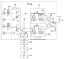
도 1a는 본 개시의 양상에 따른 다이플렉서를 이용하는 RFFE(radio frequency (RF) front end) 모듈의 개략도이다.
[0012]
도 1b는 본 개시의 양상들에 따른 캐리어 어그리게이션을 제공하기 위한 칩셋에 대해 다이플렉서들을 이용하는 RFFE(radio frequency (RF) front end) 모듈의 개략도이다.
[0013]
도 2a는 본 개시의 양상에 따른 다이플렉서 설계의 도면이다.
[0014]
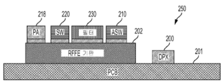
도 2b는 본 개시의 양상에 따른 RF(radio frequency) 프론트 엔드 모듈의 도면이다.
[0015]
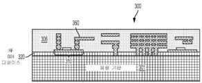
도 3a 내지 도 3e는 본 개시의 양상들에 따른 층 전사 프로세스 동안 집적 RF(radio frequency) 회로 구조의 단면도들을 도시한다.
[0016]
도 4는 본 개시의 양상들에 따른 층 전사 프로세스를 사용하여 제조된 집적 RF(radio frequency) 회로 구조의 단면도이다.
[0017]
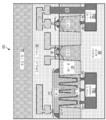
도 5는 본 개시의 양상에 따른 백사이드 바디 콘택트를 갖는 딥 트렌치 능동 디바이스를 포함하는 집적 회로 구조의 단면도이다.
[0018]
도 6은 본 개시의 다른 양상에 따른 백사이드 바디 콘택트를 갖는 딥 트렌치 능동 디바이스를 포함하는 집적 회로 구조의 단면도이다.
[0019]
도 7은 본 개시의 추가적 양상에 따른 백사이드 바디 콘택트를 갖는 딥 트렌치 능동 디바이스를 포함하는 집적 회로 구조의 단면도이다.
[0020]
도 8은 본 개시의 다른 양상에 따른 백사이드 바디 콘택트를 갖는 딥 트렌치 능동 디바이스를 포함하는 집적 회로 구조의 단면도이다.
[0021]
도 9는 본 개시의 양상에 따른 백사이드 바디 콘택트를 갖는 딥 트렌치 능동 디바이스를 포함하는 집적 회로 구조를 구성하는 방법을 예시하는 프로세스 흐름도이다.
[0022]
도 10은 본 개시의 구성이 유리하게 이용될 수 있는 예시적인 무선 통신 시스템을 도시하는 블록도이다.
[0023]
도 11은 일 구성에 따른 반도체 컴포넌트의 회로, 레이아웃 및 로직 설계에 사용되는 설계 워크스테이션을 예시하는 블록도이다.[0010] For a more thorough understanding of the present disclosure, reference is now made to the following descriptions taken in conjunction with the accompanying drawings.
[0011] FIG. 1A is a schematic diagram of a radio frequency (RF) front end module using a diplexer in accordance with aspects of the present disclosure.
[0012] FIG. 1B is a schematic diagram of a radio frequency (RF) front end module using diplexers for a chipset to provide carrier aggregation in accordance with aspects of the present disclosure.
[0013] FIG. 2a is a diagram of a diplexer design in accordance with aspects of the present disclosure.
[0014] FIG. 2B is a diagram of a radio frequency (RF) front end module in accordance with aspects of the present disclosure.
[0015] Figures 3A-3E illustrate cross-sectional views of an integrated radio frequency circuit structure during a layer transfer process in accordance with aspects of the present disclosure.
[0016] FIG. 4 is a cross-sectional view of an integrated radio frequency circuit structure fabricated using a layer transfer process in accordance with aspects of the present disclosure.
[0017] FIG. 5 is a cross-sectional view of an integrated circuit structure including a deep trench active device having a backside body contact in accordance with aspects of the present disclosure.
[0018] FIG. 6 is a cross-sectional view of an integrated circuit structure including a deep trench active device having a backside body contact in accordance with another aspect of the present disclosure.
[0019] FIG. 7 is a cross-sectional view of an integrated circuit structure including a deep trench active device having a backside body contact in accordance with a further aspect of the present disclosure.
[0020] FIG. 8 is a cross-sectional view of an integrated circuit structure including a deep trench active device having a backside body contact in accordance with another aspect of the present disclosure.
[0021] FIG. 9 is a process flow diagram illustrating a method of configuring an integrated circuit structure including a deep trench active device having a backside body contact in accordance with aspects of the present disclosure.
[0022] FIG. 10 is a block diagram illustrating an exemplary wireless communication system in which the configurations of the present disclosure may be advantageously employed.
[0023] FIG. 11 is a block diagram illustrating a design workstation for use in circuitry, layout, and logic design of semiconductor components in accordance with one arrangement.
[0024] 첨부 도면들과 관련하여 아래에 기술되는 상세한 설명은 다양한 구성들의 설명으로 의도되며, 본 명세서에서 설명된 개념들이 실시될 수 있는 유일한 구성들을 표현하도록 의도되는 것은 아니다. 상세한 설명은 다양한 개념들의 철저한 이해를 제공할 목적으로 특정 세부사항들을 포함한다. 그러나, 이러한 특정 세부사항들 없이도 이러한 개념들이 실시될 수 있음은 당업자들에게 자명할 것이다. 일부 예들에서, 이러한 개념들을 불명료하게 하는 것을 피하기 위해, 잘 알려진 구조들 및 컴포넌트들은 블록도 형태로 도시된다. 본 명세서에 설명된 바와 같이, "및/또는"이라는 용어의 사용은 "포함적 논리합(inclusive OR)"을 표현하도록 의도되고, "또는"이라는 용어의 사용은 "배타적 논리합(exclusive OR)"을 표현하도록 의도된다.[0024] The following detailed description with reference to the accompanying drawings is intended as a description of various configurations and is not intended to represent the only configurations in which the concepts described herein may be practiced. The detailed description includes specific details for the purpose of providing a thorough understanding of the various concepts. However, it will be apparent to those skilled in the art that these concepts may be practiced without these specific details. In some instances, well-known structures and components are shown in block diagram form in order to avoid obscuring these concepts. As used herein, the use of the term " and / or " is intended to represent " inclusive OR ", and the use of the term " It is intended to express.
[0025] 모바일 RF(radio frequency) 칩 설계들(예를 들어, 모바일 RF 트랜시버들)은 비용 및 전력 소비 고려사항들로 인해 딥 서브-마이크론 프로세스 노드로 이동해왔다. 모바일 RF 트랜시버들의 설계 복잡도는 캐리어 어그리게이션과 같은 통신 향상들을 지원하기 위해 추가된 회로 기능들에 의해 추가로 복잡하게 된다.[0025] Mobile radio frequency (RF) chip designs (e.g., mobile RF transceivers) have moved to deep sub-micron process nodes due to cost and power consumption considerations. The design complexity of mobile RF transceivers is further complicated by the added circuit functionality to support communication enhancements such as carrier aggregation.
[0026] 이러한 모바일 RF 트랜시버들의 설계는 SOI(silicon on insulator) 기술의 사용을 포함할 수 있다. SOI 기술은 기생 디바이스 커패시턴스를 감소시키고 성능을 개선하기 위해 종래의 실리콘 기판들을 계층화된 실리콘-절연체-실리콘 기판으로 대체한다. SOI-기반 디바이스들은 종래의 실리콘-구축 디바이스들과 상이한데, 이는 실리콘 접합이 통상적으로 BOX(buried oxide) 층인 전기 절연체 위에 있기 때문이며, 여기서 BOX 층의 두께는 감소될 수 있다. 그러나, 감소된 두께의 BOX 층은 BOX 층을 지지하는 기판과 실리콘 층 상의 능동 디바이스의 근접도에 의해 초래되는 기생 커패시턴스를 충분히 감소시키지 않을 수 있다.[0026] The design of these mobile RF transceivers may include the use of silicon on insulator (SOI) technology. SOI technology replaces conventional silicon substrates with layered silicon-insulator-silicon substrates to reduce parasitic device capacitance and improve performance. SOI-based devices differ from conventional silicon-building devices because the silicon junction is on an electrical insulator, which is typically a BOX (buried oxide) layer, where the thickness of the BOX layer can be reduced. However, the BOX layer of reduced thickness may not sufficiently reduce the parasitic capacitance caused by the proximity of the substrate supporting the BOX layer and the active device on the silicon layer.
[0027] SOI 기술을 사용하여 제조된 트랜지스터는 일반적으로 플로팅 바디(floating body) 효과를 겪고, 여기서 트랜지스터의 바디는 절연된 기판에 대해 커패시터를 형성한다. 이러한 어레인지먼트에서, 커패시터 상에 누적된 전하는 악영향들, 예를 들어, 구조에서의 기생 트랜지스터들 및 오프-상태 누설 뿐만 아니라 이의 이전 상태들에 대한 트랜지스터의 임계 전압의 의존도를 초래한다. 플로팅 바디 효과는 특히 아날로그 디바이스들에서 극심한데, 여기서 임계 전압 제어 및 바디 충전 제어는 플로팅 바디 효과에 의해 방지된다. 플로팅 바디 효과를 방지하기 위해 바디 콘택트가 사용될 수 있다. 불행하게도, 바디 콘택트의 사용은 영역 패널티를 초래한다. 그 결과, 본 개시의 양상들은 딥 트렌치 능동 디바이스에 대한 백사이드 바디 연결의 형성을 가능하게 하는 층 전사 후 프로세스(post-layer transfer process)를 포함한다.[0027] A transistor fabricated using SOI technology typically undergoes a floating body effect, where the body of the transistor forms a capacitor to an insulated substrate. In such an arrangement, the accumulated charge on the capacitor results in adverse effects, e.g., dependence of the threshold voltage of the transistor on its previous states as well as off-state leakage and parasitic transistors in the structure. Floating body effects are particularly acute in analog devices, where threshold voltage control and body charge control are prevented by floating body effects. Body contacts can be used to prevent floating body effects. Unfortunately, the use of body contacts results in area penalties. As a result, aspects of the present disclosure include a post-layer transfer process that enables the formation of a backside body connection to a deep trench active device.
[0028] 집적 회로 구조의 반도체 제조에 대한 프로세스 흐름은 FEOL(front-end-of-line) 프로세스들, MOL(middle-of-line)(또한, MEOL(middle-end-of-line)로 지칭됨) 프로세스들 및 BEOL(back-end-of-line) 프로세스들을 포함할 수 있다. FEOL 프로세스는 이온 주입, 어닐링, 산화, CVD(chemical vapor deposition) 또는 ALD(atomic layer deposition) 에칭, CMP(chemical mechanical polishing), 에피택시를 포함한다. MOL 프로세스들은 BEOL 상호연결부들에 대한 트랜지스터들의 연결을 가능하게 하는 프로세스 단계들의 세트를 포함할 수 있다. 이러한 단계들은 실리시데이션(silicidation) 및 콘택트 형성 뿐만 아니라 응력 도입을 포함한다. BEOL 프로세스들은 독립적 트랜지스터들을 연결하고 회로들을 형성하는 상호연결부를 형성하는 프로세스 단계들의 세트를 포함할 수 있다.[0028] The process flow for semiconductor fabrication of integrated circuit structures is called front-end-of-line (FEOL) processes, middle-of-line (MOL) And back-end-of-line (BEOL) processes. The FEOL process includes ion implantation, annealing, oxidation, chemical vapor deposition (CVD) or atomic layer deposition (ALD) etching, chemical mechanical polishing (CMP), and epitaxy. MOL processes may include a set of process steps that enable the connection of transistors to the BEOL interconnects. These steps include stress induction as well as silicidation and contact formation. BEOL processes may include a set of process steps that form interconnects that connect independent transistors and form circuits.
[0029] 본 개시의 양상들은 고품질(Q)-팩터 RF(radio frequency) 애플리케이션들에 대한 집적 RF 회로 구조들에서 안테나 스위치 트랜지스터로서 사용될 수 있는 백사이드 바디 콘택트를 갖는 딥 트렌치 스위치 트랜지스터를 설명한다. 일 구성에서, 층 전사 전 프로세스(pre-layer transfer process)가 딥 트렌치 트랜지스터를 형성한다. 또한, 층 전사 후 프로세스는 딥 트렌치 스위치 트랜지스터의 바디를 연결하는 백사이드 바디 콘택트를 형성한다. 백사이드 바디 연결을 형성하는 층 전사 후 프로세스는 종래의 바디 콘택트들과 연관된 영역 패널티 또는 원치 않는 저항 경로들을 회피하면서 딥 스위치 트랜지스터의 바디가 부동하는 것을 방지함으로써 SOI 디바이스들과 연관된 플로팅 바디 효과 문제를 해결한다.[0029] Aspects of the present disclosure describe a deep trench switch transistor having a backside body contact that can be used as an antenna switch transistor in integrated RF circuit structures for high quality (Q) -factor RF (radio frequency) applications. In one configuration, a pre-layer transfer process forms a deep trench transistor. In addition, the post-layer transfer process forms a backside body contact connecting the body of the deep trench switch transistor. The post-layer transfer process that forms the backside body connection solves the floating body effect problem associated with SOI devices by preventing the body of the dip switch transistor from floating, while avoiding area penalty or unwanted resistance paths associated with conventional body contacts. do.
[0030]
도 1a는 본 개시의 양상에 따른 다이플렉서(200)를 이용하는 RFFE(radio frequency (RF) front end) 모듈(100)의 개략도이다. RF 프론트 엔드 모듈(100)은 전력 증폭기들(102), 듀플렉서/필터들(104), 및 RF(radio frequency) 스위치 모듈(106)을 포함한다. 전력 증폭기들(102)은 신호(들)를 송신을 위한 특정 전력 레벨로 증폭한다. 듀플렉서/필터들(104)은 주파수, 삽입 손실, 거부 또는 다른 유사한 파라미터들을 포함하는 다양한 상이한 파라미터들에 따라 입력/출력 신호들을 필터링한다. 또한, RF 스위치 모듈(106)은 RF 프론트 엔드 모듈(100)의 나머지 상에 전달할 입력 신호들의 특정 부분들을 선택할 수 있다.[0030]
1A is a schematic diagram of a radio frequency (RF)
[0031]
RF 프론트 엔드 모듈(100)은 또한 튜너 회로(112)(예를 들어, 제1 튜너 회로(112A) 및 제2 튜너 회로(112B)), 다이플렉서(200), 커패시터(116), 인덕터(118), 접지 단자(115) 및 안테나(114)를 포함한다. 튜너 회로(112)(예를 들어, 제1 튜너 회로(112A) 및 제2 튜너 회로(112B))는 튜너, PDET(portable data entry terminal) 및 HKADC(house keeping analog to digital converter)와 같은 컴포넌트들을 포함한다. 튜너 회로(112)는 안테나(114)에 대한 임피던스 튜닝(예를 들어, VSWR(voltage standing wave ratio) 최적화)을 수행할 수 있다. RF 프론트 엔드 모듈(100)은 또한 WTR(wireless transceiver)(120)에 커플링된 수동 결합기(108)를 포함한다. 수동 결합기(108)는 제1 튜너 회로(112A) 및 제2 튜너 회로(112B)로부터 검출된 전력을 결합한다. 무선 트랜시버(120)는 수동 결합기(108)로부터 정보를 프로세싱하고 이러한 정보를 모뎀(130)(예를 들어, MSM(mobile station modem))에 제공한다. 모뎀(130)은 AP(application processor)(140)에 디지털 신호를 제공한다.[0031]
The RF
[0032]
도 1a에 도시된 바와 같이, 다이플렉서(200)는 튜너 회로(112)의 튜너 컴포넌트와 커패시터(116), 인덕터(118) 및 안테나(114) 사이에 있다. 다이플렉서(200)는 무선 트랜시버(120), 모뎀(130) 및 애플리케이션 프로세서(140)를 포함하는 칩셋에 RF 프론트 엔드 모듈(100)로부터의 높은 시스템 성능을 제공하기 위해 안테나(114)와 튜너 회로(112) 사이에 배치될 수 있다. 다이플렉서(200)는 또한 고대역 주파수들 및 저대역 주파수들 둘 모두에 대해 주파수 도메인 멀티플렉싱을 수행한다. 다이플렉서(200)가 입력 신호들에 대해 자신의 주파수 멀티플렉싱 기능들을 수행한 후, 다이플렉서(200)의 출력은 커패시터(116) 및 인덕터(118)를 포함하는 선택적 LC(인덕터/커패시터) 네트워크에 공급된다. LC 네트워크는 원하는 경우 안테나(114)에 대한 여분의 임피던스 매칭 컴포넌트들을 제공할 수 있다. 그 다음, 특정 주파수를 갖는 신호가 안테나(114)에 의해 송신되거나 수신된다. 단일 커패시터 및 인덕터가 도시되어 있지만, 다수의 컴포넌트들이 또한 고려된다.[0032]
The
[0033]
도 1b는 본 개시의 양상에 따른 캐리어 어그리게이션을 제공하기 위해 칩셋(160)에 대한 제1 다이플렉서(200-1)를 포함하는 WLAN(wireless local area network)(예를 들어, WiFi) 모듈(170) 및 제2 다이플렉서(200-2)를 포함하는 RF 프론트 엔드 모듈(150)의 개략도이다. WiFi 모듈(170)은 무선 로컬 영역 네트워크 모듈(예를 들어, WLAN 모듈(172))에 안테나(192)를 통신가능하게 커플링하는 제1 다이플렉서(200-1)를 포함한다. RF 프론트 엔드 모듈(150)은 듀플렉서(180)를 통해 WTR(wireless transceiver)(120)에 안테나(194)를 통신가능하게 커플링하는 제2 다이플렉서(200-2)를 포함한다. 무선 트랜시버(120) 및 WiFi 모듈(170)의 WLAN 모듈(172)은 PMIC(power management integrated circuit)(156)를 통해 전원(152)에 의해 전력공급되는 모뎀(MSM, 예를 들어, 기저대역 모뎀)(130)에 커플링된다. 칩셋(160)은 또한 신호 무결성을 제공하기 위해 커패시터들(162 및 164) 뿐만 아니라 인덕터(들)(166)를 포함한다. PMIC(156), 모뎀(130), 무선 트랜시버(120) 및 WLAN 모듈(172) 각각은 커패시터들(예를 들어, 158, 132, 122 및 174)을 포함하고 클럭(154)에 따라 동작한다. 칩셋(160)의 다양한 인덕터 및 커패시터 컴포넌트들의 기하구조 및 어레인지먼트는 컴포넌트들 사이의 전자기 커플링을 감소시킬 수 있다.[0033]
1B illustrates a wireless local area network (WLAN) (e.g., WiFi) system including a first diplexer 200-1 for the
[0034]
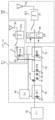
도 2a는 본 개시의 양상에 따른 다이플렉서(200)의 도면이다. 다이플렉서(200)는 HB(high band) 입력 포트(212), LB(low band) 입력 포트(214) 및 안테나(216)를 포함한다. 다이플렉서(200)의 고대역 경로는 고대역 안테나 스위치(210-1)를 포함한다. 다이플렉서(200)의 저대역 경로는 저대역 안테나 스위치(210-2)를 포함한다. RF 프론트 엔드 모듈을 포함하는 무선 디바이스는 무선 디바이스의 RF 입력 및 RF 출력에 대한 광범위 대역을 가능하게 하기 위해 안테나 스위치들(210) 및 다이플렉서(200)를 사용할 수 있다. 또한, 안테나(216)는 MIMO(multiple input, multiple output) 안테나일 수 있다. 다중 입력, 다중 출력 안테나들은 캐리어 어그리게이션과 같은 특징들을 지원하기 위해 무선 디바이스들의 RF 프론트 엔드에 널리 사용될 것이다.[0034]
2A is a diagram of a
[0035]
도 2b는 본 개시의 양상에 따른 RF 프론트 엔드 모듈(250)의 도면이다. RF 프론트 엔드 모듈(250)은 도 2a에서 언급된 광범위 대역을 가능하게 하기 위해 ASW(antenna switch)(210) 및 다이플렉서(200)(또는 트리플렉서)를 포함한다. 또한, RF 프론트 엔드 모듈(250)은 필터들(230), RF 스위치(220) 및 기판(202)에 의해 지원되는 전력 증폭기들(218)을 포함한다. 필터들(230)은, RF 프론트 엔드 모듈(250)에서 고차 고조파들을 방지하기 위해 다이플렉서, 트리플렉서, 저역 통과 필터들, 밸룬(balun) 필터들 및/또는 노치 필터들을 형성하기 위해 기판(202)과 함께 배열된 인덕터들(L) 및 커패시터들(C)을 갖는 다양한 LC 필터들을 포함할 수 있다. 다이플렉서(200)는 시스템 보드(201)(예를 들어, PCB(printed circuit board) 또는 패키지 기판) 상에 SMD(surface mount device)로서 구현될 수 있다. 대안적으로, 다이플렉서(200)는 기판(202) 상에 구현될 수 있다.[0035]
2B is a diagram of an RF
[0036]
이러한 구성에서, RF 프론트 엔드 모듈(250)은 RF 프론트 엔드 모듈(250)에서 고차 고조파들을 감소시키는 것을 돕는 SOI(silicon on insulator) 기술을 사용하여 구현된다. SOI 기술은 기생 디바이스 커패시턴스를 감소시키고 성능을 개선하기 위해 종래의 실리콘 기판들을 계층화된 실리콘-절연체-실리콘 기판으로 대체한다. SOI-기반 디바이스들은 종래의 실리콘-구축 디바이스들과 상이한데, 이는 실리콘 접합이 통상적으로 BOX(buried oxide) 층인 전기 절연체 위에 있기 때문이다. 그러나, 감소된 두께의 BOX 층은 BOX 층을 지지하는 기판과 (실리콘 층 상의) 능동 디바이스 사이의 근접도에 의해 초래되는 기생 커패시턴스를 충분히 감소시키지 않을 수 있다. 그 결과, 본 개시의 양상들은 도 3a 내지 도 3e에 도시된 바와 같이, 기판으로부터 능동 디바이스를 추가로 분리시키는 층 전사 프로세스를 포함한다.[0036]
In this configuration, the RF
[0037]
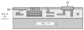
도 3a 내지 도 3e는 본 개시의 양상들에 따른 층 전사 프로세스 동안 집적 RF(radio frequency) 회로 구조(300)의 단면도들을 도시한다. 도 3a에 도시된 바와 같이, RF SOI(silicon on insulator) 디바이스는 희생 기판(301)(예를 들어, 벌크 웨이퍼)에 의해 지지되는 BOX(buried oxide) 층(320) 상에 능동 디바이스(310)를 포함한다. RF SOI 디바이스는 또한 제1 유전체 층(306) 내의 능동 디바이스(310)에 커플링된 상호연결부들(350)을 포함한다. 도 3b에 도시된 바와 같이, 핸들 기판(302)은 제1 유전체 층(306)에 본딩된다.[0037]
3A-3E illustrate cross-sectional views of an integrated RF (radio frequency)
[0038]
도 3b에 도시된 바와 같이, 핸들 기판(302)은 RF SOI 디바이스의 프론트-사이드 유전체 층(306)에 본딩된다. 또한, 희생 기판(301)이 제거된다. 층 전사 프로세스를 사용한 희생 기판(301)의 제거는 유전체 두께를 증가시킴으로써 고성능, 저-기생 RF 디바이스들을 가능하게 한다. 즉, RF SOI 디바이스의 기생 커패시턴스는 유전체 두께에 비례하고, 이는 능동 디바이스(310)와 핸들 기판(302) 사이의 거리를 결정한다.[0038]
As shown in FIG. 3B, the
[0039]
도 3c에 도시된 바와 같이, RF SOI 디바이스는 핸들 기판(302)이 고정되고 희생 기판(301)이 제거되면 플립(flip)된다. 도 3d에 도시된 바와 같이, 층 전사 후 금속배선 프로세스는 예를 들어, 정규의 CMOS(complementary metal oxide semiconductor) 프로세스를 사용하여 수행된다. 도 3e에 도시된 바와 같이, 집적 RF 회로 구조(300)는 패시베이션 층을 증착하고, 본드 패드들을 개방하고, 재분포 층을 증착하고, 집적 RF 회로 구조(300)의 시스템 보드(예를 들어, PCB(printed circuit board))에의 본딩을 가능하게 하기 위해 전도성 범프들/기둥들을 형성함으로써 완료된다.[0039]
As shown in FIG. 3C, the RF SOI device is flipped when the
[0040]
도 3a를 다시 참조하면, RF SOI 디바이스는 희생 기판(301)과 BOX 층(320) 사이에 트랩 풍부 층을 포함할 수 있다. 또한, 희생 기판(301)은 핸들 기판(302)으로 대체될 수 있고, BOX 층(320)의 두께는 고조파들을 개선하기 위해 증가될 수 있다. RF SOI 디바이스의 이러한 어레인지먼트는 순수 실리콘 또는 SOI 구현에 비해 개선된 고조파들을 제공할 수 있지만, RF SOI 디바이스는 특히 실리콘 핸들 기판이 사용되는 경우 핸들 기판으로부터의 비선형 응답들에 의해 제한된다. 즉, 도 3a에서, BOX 층(320)의 증가된 두께는 도 3b 내지 도 3e에 도시된 구성들에 비해 능동 디바이스(310)와 희생 기판(301) 사이에 충분한 거리를 제공하지 않는다. 또한, RF SOI 디바이스는 일반적으로 SOI 층의 일 사이드 상의 CMOS 트랜지스터 형성으로 제한된다.[0040]
Referring again to FIG. 3A, the RF SOI device may include a trap-rich layer between the sacrificial substrate 301 and the
[0041]
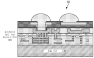
도 4는 본 개시의 양상들에 따른 층 전사 프로세스를 사용하여 제조된 집적 RF 회로 구조(400)의 단면도이다. 대표적으로, 집적 RF 회로 구조(400)는 절연 층(430) 상에 형성된 게이트, 바디 및 소스/드레인 영역들을 갖는 능동 디바이스(410)를 포함한다. SOI(silicon on insulator) 구현들에서, 절연 층(430)은 BOX(buried oxide) 층이고, 바디 및 소스/드레인 영역들은 BOX 층에 의해 지원되는 STI(shallow trench isolation) 영역들을 포함하는 SOI 층으로부터 형성된다.[0041]
4 is a cross-sectional view of an integrated
[0042]
집적 RF 회로 구조(400)는 또한 능동 디바이스(410)의 소스/드레인 영역들에 커플링된 MEOL(middle-end-of-line)/BEOL(back-end-of-line) 상호연결부들을 포함한다. 설명된 바와 같이, MEOL/BEOL 층들은 프론트-사이드 층들로 지칭된다. 반대로, 절연 층(430)을 지지하는 층들은 백사이드 층들로 지칭될 수 있다. 이러한 명명법에 따라, 프론트-사이드 상호연결부(470)는 프론트-사이드 유전체 층(404)의 프론트-사이드 콘택트들(412)을 통해 능동 디바이스(410)의 소스/드레인 영역들에 커플링된다. 또한, 핸들 기판(402)은 프론트-사이드 유전체 층(404)에 커플링된다. 이러한 구성에서, 백사이드 유전체(440)는 절연 층(430)에 인접하고 가능하게는 이를 지지한다. 또한, 백사이드 금속배선(450)은 프론트-사이드 상호연결부(470)에 커플링된다.[0042]
[0043]
도 4에 도시된 바와 같이, 층 전사 프로세스는 집적 RF 회로 구조(400)의 고조파들을 개선하기 위해 능동 디바이스(410)와 핸들 기판(402) 사이의 분리를 증가시킨다. 층 전사 프로세스는 고성능 저-기생 RF 디바이스들을 가능하게 하는 한편, 집적 RF 회로 구조(400)는 플로팅 바디 효과를 겪을 수 있다. 즉, SOI 기술을 사용하여 제조된 능동 디바이스들은 일반적으로 플로팅 바디 효과를 겪고, 여기서 트랜지스터의 바디는 절연된 기판에 대해 커패시터를 형성한다. 플로팅 바디 효과는 특히 아날로그 디바이스들에서 극심한데, 여기서 임계 전압 제어 및 바디 충전 제어는 플로팅 바디 효과에 의해 방지된다. 플로팅 바디 효과를 방지하기 위해 바디 콘택트가 사용될 수 있다. 불행하게도, 바디 콘택트의 사용은 상당한 영역 패널티를 초래한다. 그 결과, 본 개시의 양상들은 딥 트렌치 능동 디바이스에 대한 백사이드 바디 연결의 형성을 가능하게 하는 층 전사 후 프로세스(post-layer transfer process)를 포함한다.[0043]
4, the layer transfer process increases the separation between the
[0044] 본 개시의 다양한 양상들은 집적 회로 구조에 대해 백사이드 바디 연결의 형성을 가능하게 하는 층 전사 후 프로세스를 위한 기술들을 제공한다. 반대로, FEOL(front-end-of-line) 프로세스 동안 형성된 능동 디바이스들에 대한 액세스는 종래에, 능동 디바이스들의 게이트들 및 소스/드레인 영역들과 BEOL(back-end-of-line) 상호연결부 층들(예를 들어, M1, M2 등) 사이의 콘택트들을 제공하는 MEOL(middle-end-of-line) 프로세싱 동안 제공된다. 본 개시의 양상들은 고품질(Q)-팩터 RF(radio frequency) 애플리케이션들에 대한 집적 RF 회로 구조들에서 안테나 스위치 트랜지스터들로서 사용될 수 있는 백사이드 바디 연결들을 갖는 딥 트렌치 스위치 트랜지스터들을 형성하기 위한 층 전사 후 프로세스를 수반한다. 다른 애플리케이션들은 낮은 전력 증폭기 모듈, 저잡음 증폭기 및 안테나 다이버시티 스위치 내의 능동 디바이스를 포함한다.[0044] The various aspects of the present disclosure provide techniques for a post-layer transfer process that enables the formation of a backside body connection to an integrated circuit structure. Conversely, access to active devices formed during a front-end-of-line (FEOL) process has traditionally been achieved with gates and source / drain regions of active devices and back-end- Is provided during middle-end-of-line (MEOL) processing, which provides contacts between a plurality of contacts (e.g., M1, M2, etc.). Aspects of the present disclosure relate to post-layer transfer processes to form deep trench switch transistors with backside body connections that can be used as antenna switch transistors in integrated RF circuit structures for high-quality (Q) -factor radio frequency (RF) ≪ / RTI > Other applications include low power amplifier modules, low noise amplifiers, and active devices in antenna diversity switches.
[0045]
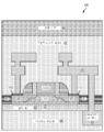
도 5는 본 개시의 양상들에 따른 백사이드 바디 연결을 갖는 딥 트렌치 능동 디바이스(예를 들어, 스위치 트랜지스터)를 포함하는 집적 회로 구조(500)의 단면도이다. 본 개시의 양상들에서, 층 전사 후 프로세스는 백사이드 바디 연결의 형성을 가능하게 하고, 이는 절연체 제조 프로세스들 상의 종래의 실리콘과 연관된 플로팅 바디 효과를 해결한다. 대표적으로, 집적 회로 구조(500)는 절연 층(530)의 프론트-사이드 표면 상에서 절연 층(530)의 백사이드 표면까지 확장되는 딥 트렌치 능동 디바이스(510)를 포함한다. 이러한 구성에서, 딥 트렌치 능동 디바이스(510)의 바디는 반도체 층(예를 들어, SOI 구현을 위한 실리콘)으로부터 형성된 반도체 기둥들(512)로 구성된다. 기둥들은 더 작은 영역에서 더 긴 길이가 획득되는 한(예를 들어, "아코디언" 효과) 근접하게 이격될 필요가 없다. 또한, 게이트는 반도체 기둥들(512)과 서로 맞물리고 유전체 재료 층(522)(예를 들어, 게이트 유전체)에 의해 분리되고 절연 층(530)을 통해 확장되는 게이트 핑거들(520)로 구성된다.[0045]
5 is a cross-sectional view of an
[0046]
절연 층(530)은 SOI(silicon on insulator) 구현을 위한 BOX(buried oxide) 층일 수 있고, 여기서 바디 및 소스/드레인 영역들(미도시)은 SOI 층으로부터 형성된다. 대안적으로, 절연 층(530)은 딥 트렌치 능동 디바이스(510)를 제1 트렌치-타입 능동 디바이스(580) 및 제2 트렌치-타입 능동 디바이스(590)로부터 절연하는 딥 트렌치 분리 영역일 수 있다. 제1 트렌치-타입 능동 디바이스(580) 및 제2 트렌치-타입 능동 디바이스(590)에 관한 추가적인 세부사항들은 본 개시의 세부사항들을 모호하게 하는 것을 회피하기 위해 생략된다. 또한, 트렌치-타입 스위치 트랜지스터들은 딥 트렌치 스위치 트랜지스터의 드레인 영역 및 소스 영역을 제공하기 위해 n-타입(예를 들어, 제1 도핑된 영역) 및 p-타입(예를 들어, 제2 도핑된 영역) 반도체 영역들을 도핑하기 위한 주입 프로세스에 따라, NMOS(negative metal oxide semiconductor) 스위치 트랜지스터들 또는 포지티브 MOS(PMOS 트랜지스터들)로서 구성될 수 있다.[0046]
The insulating
[0047]
본 개시의 이러한 양상에서, 집적 회로 구조(500)는 또한 절연 층(530)의 프론트-사이드 표면에 대향하는 백사이드 표면을 지지하는 백사이드 유전체 층(540)에 배열된 백사이드 금속배선(550)을 포함한다. 본 개시의 양상들에 따른 백사이드 금속배선(550)은 딥 트렌치 능동 디바이스(510)에 대한 낮은 저항 바디 연결을 제공한다. 이러한 어레인지먼트에서, 백사이드 금속배선(550)의 제1 부분(550-1)은 콘택트 플러그들(552) 및 백사이드 실리사이드 층(554)을 통해 딥 트렌치 능동 디바이스(510)의 바디에 전기적으로 커플링된다. 딥 트렌치 능동 디바이스(510)의 이러한 구성은 백사이드 금속배선(550)을 바디에 전기적으로 커플링함으로써 플로팅 바디 효과를 방지한다.[0047]
The integrated
[0048]
집적 회로 구조(500)는 또한 프론트-사이드 유전체 층(504)에 배열된 프론트-사이드 금속배선(570)(예를 들어, 제1 BEOL 상호연결부(M1))을 포함한다. 프론트-사이드 금속배선(570)은 비아(560)를 통해 백사이드 금속배선(550)의 제2 부분(550-2)에 커플링된다. 백사이드 유전체 층(540) 내의 백사이드 금속배선(550)의 제2 부분(550-2)은 콘택트 플러그들(552) 및 백사이드 실리사이드 층(554) 중 하나를 통해 제2 트렌치-타입 능동 디바이스(590)의 바디에 전기적으로 커플링된다. 또한, 핸들 기판(502)은 프론트-사이드 유전체 층(504)에 커플링된다. 백사이드 유전체 층(540)는 절연 층(530)에 인접하고 가능하게는 이를 지지한다. 이러한 구성에서, 층 전사 후 금속배선 프로세스는 백사이드 금속배선(550)을 형성한다. 도 5에 도시된 바와 같이, 프론트-사이드 금속배선(570)은 백사이드 금속배선(550)으로부터 원위에 배열된다.[0048]
The integrated
[0049] 본 개시의 양상들에 따르면, 핸들 기판(502)은 실리콘과 같은 반도체 재료로 구성될 수 있다. 이러한 구성에서, 핸들 기판(502)은 적어도 하나의 다른 능동 디바이스를 포함할 수 있다. 대안적으로, 핸들 기판(502)은 기생 커패시턴스를 감소시킴으로써 고조파들을 추가로 개선하기 위한 수동 기판일 수 있다. 이러한 구성에서, 핸들 기판(502)은 적어도 하나의 다른 수동 디바이스를 포함할 수 있다. 본원에서 설명된 바와 같이, "수동 기판"이라는 용어는 다이싱된 웨이퍼 또는 패널의 기판을 지칭할 수 있거나 또는 다이싱되지 않은 웨이퍼/패널의 기판을 지칭할 수 있다. 일 구성에서, 수동 기판은 유리, 공기, 석영, 사파이어, 높은 비저항 실리콘 또는 다른 유사한 수동 재료로 구성된다. 수동 기판은 또한 코어리스(coreless) 기판일 수 있다.[0049] According to aspects of the present disclosure, the handle substrate 502 may be comprised of a semiconductor material such as silicon. In such an arrangement, the handle substrate 502 may include at least one other active device. Alternatively, the handle substrate 502 may be a passive substrate to further improve harmonics by reducing parasitic capacitance. In such an arrangement, the handle substrate 502 may include at least one other passive device. As described herein, the term " passive substrate " may refer to a substrate of a diced wafer or panel, or may refer to a substrate of a wafer / panel that is not diced. In one configuration, the passive substrate is comprised of glass, air, quartz, sapphire, high resistivity silicon or other similar passive material. The passive substrate may also be a coreless substrate.
[0050] "층"이라는 용어는 막을 포함하고, 달리 언급되지 않으면 수직 또는 수평 두께를 표시하는 것으로 해석되지 않아야 하는 것으로 이해될 것이다. 본원에서 설명된 바와 같이, "기판"이라는 용어는 다이싱된 웨이퍼의 기판을 지칭할 수 있거나 또는 다이싱되지 않은 웨이퍼의 기판을 지칭할 수 있다. 유사하게, 칩 및 다이라는 용어들은 상호교환이 논리에 맞는다면 상호교환가능하게 사용될 수 있다.[0050] It is to be understood that the term " layer " includes membranes and should not be construed as indicating a vertical or horizontal thickness unless otherwise stated. As described herein, the term " substrate " may refer to a substrate of a diced wafer or may refer to a substrate of a wafer that is not diced. Similarly, the terms chip and da can be used interchangeably if the interchange is logical.
[0051]
본 개시의 양상들에서, 층 전사 후 프로세스는 도 5 내지 도 8에 도시된 바와 같이, 트렌치-타입 능동 디바이스들의 바디를 연결하기 위한 백사이드 금속배선을 형성한다. 백사이드 실리시데이션 프로세스에서의 변경들은 도 7 및 도 8에 도시되어 있다. 또한, 반도체 층(예를 들어, 실리콘 온 절연체 층)에 대한 변경들은 도 7 및 도 8에 도시되어 있다. 본 개시의 추가적 양상에 따르면, 딥 트렌치 능동 디바이스(510)는 MOS(metal oxide semiconductor) 커패시터로 구성될 수 있다. 이러한 어레인지먼트에서, MOS 커패시터는 제1 플레이트로서 게이트 핑거들(520), 제2 플레이트로서 반도체 기둥들(512) 및 커패시터 유전체로서 유전체 재료 층(522)을 포함한다.[0051]
In aspects of the present disclosure, the post-layer transfer process forms a backside metal interconnect for connecting the bodies of trench-type active devices, as shown in Figs. 5-8. Changes in the backside silicidation process are shown in FIGS. 7 and 8. FIG. Further, modifications to the semiconductor layer (for example, a silicon-on-insulator layer) are shown in Figs. 7 and 8. Fig. According to a further aspect of the present disclosure, the deep trench
[0052]
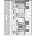
도 6은 본 개시의 양상들에 따른 백사이드 바디 연결을 갖는 트렌치-타입 능동 디바이스를 포함하는 집적 회로 구조(600)의 단면도이다. 인식될 바와 같이, 집적 회로 구조(600)의 구성은 도 5의 집적 회로 구조(500)의 구성과 유사하다. 그러나, 도 6에 도시된 구성에서, 딥 트렌치 능동 디바이스(510)의 바디의 부분들을 노출시키기 위한 실리사이드 홀들을 형성하기 위해 백-엔드-오브-라인 비아 프로세스(back-end-of-line via process)(V0)가 사용된다. 즉, 이러한 어레인지먼트에서, 백사이드 실리사이드 층(554)(도 5)은 도 5에 도시된 실리사이드 연속적 층보다 딥 트렌치 능동 디바이스(510)의 바디의 노출된 부분들 상에 이산적 엘리먼트들로서 증착된다. 또한, 백사이드 실리사이드 층(554)(도 5)은 제2 트렌치-타입 능동 디바이스(590)의 바디의 노출된 부분 상에 이산 엘리먼트들로서 증착된다.[0052]
6 is a cross-sectional view of an
[0053] 따라서, 본 개시의 이러한 양상은 또한, 트렌치 타입 능동 디바이스들의 바디를 연결하기 위한 단순화된 층 전사 후 프로세스 백사이드 실리시데이션 프로세스를 제공함으로써 종래의 실리콘 온 절연체 제조 프로세스들과 연관된 플로팅 바디 효과 문제를 해결한다. 도 6에 도시된 구성은 예를 들어, 도 7에 도시된 바와 같이 SOI 웨이퍼보다 벌크 웨이퍼를 사용하여 제조됨을 인식해야 한다.[0053] Thus, this aspect of the present disclosure also solves the floating body effect problem associated with conventional silicon-on-insulator manufacturing processes by providing a simplified post-transfer process backbone silicidation process for connecting the bodies of trench type active devices do. It should be appreciated that the configuration shown in FIG. 6 is fabricated using a bulk wafer rather than an SOI wafer, for example, as shown in FIG.
[0054]
도 7은 본 개시의 양상들에 따른 백사이드 바디 연결을 갖는 트렌치-타입 능동 디바이스를 포함하는 집적 회로 구조(700)의 단면도이다. 인식될 바와 같이, 집적 회로 구조(700)의 구성은 도 6의 집적 회로 구조(600)의 구성과 유사하다. 그러나, 도 7에 도시된 구성에서, 증가된 두께 반도체 층은 SOI 웨이퍼에 의해 지지되는 실리콘 온 절연체(SOI) 층으로서 제공된다. 이러한 어레인지먼트에서, 절연 층(530)은 딥 트렌치 능동 디바이스(510)와 제1 트렌치-타입 능동 디바이스(580) 및 제2 트렌치-타입 능동 디바이스(590) 사이의 딥 트렌치 절연 층일 수 있다.[0054]
7 is a cross-sectional view of an
[0055]
이러한 어레인지먼트에 따르면, 딥 트렌치 능동 디바이스(510)의 바디는 또한 절연 층(530)에 의해 지지된다. 콘택트 플러그들(552)은 절연 층(530)의 일부를 통해 확장된다. 또한, 백사이드 금속배선(550)의 제1 부분(550-1) 및 제2 부분(550-2)은 딥 트렌치 능동 디바이스(510) 및 제2 트렌치-타입 능동 디바이스(590)를 연결하기 위해 절연 층(530)의 일부 및 백사이드 유전체 층(540)의 일부에 형성된다. 따라서, 본 개시의 이러한 양상은 종래의 실리콘 온 절연체 제조 프로세스들과 연관된 플로팅 바디 효과 문제를 해결한다.[0055]
According to this arrangement, the body of the deep trench
[0056]
도 8은 본 개시의 양상들에 따른 백사이드 바디 연결을 갖는 트렌치-타입 능동 디바이스를 포함하는 집적 회로 구조(800)의 단면도이다. 인식될 바와 같이, 집적 회로 구조(800)의 구성은 도 6의 집적 회로 구조(600)의 구성과 유사하다. 그러나, 도 8에 도시된 구성에서, 감소된 두께 반도체 층은 SOI 웨이퍼에 의해 지지되는 실리콘 온 절연체(SOI) 층으로서 제공된다. 이러한 어레인지먼트에서, 절연 층(530)은 딥 트렌치 능동 디바이스(510)와 제1 트렌치-타입 능동 디바이스(580) 및 제2 트렌치-타입 능동 디바이스(590) 사이의 딥 트렌치 절연 층(532)과 결합된다. 본 개시의 일 양상에서, 대체 게이트 프로세스는, 개선된 게이트 형성을 위해 폴리 에칭 제한들(예를 들어, 라인/에지 거칠기)를 극복하기 위해, 딥 트렌치 능동 디바이스(510) 및/또는 제1 트렌치-타입 능동 디바이스(580) 및 제2 트렌치-타입 능동 디바이스(590)를 제조하기 위해 수행될 수 있다.[0056]
8 is a cross-sectional view of an
[0057]
이러한 어레인지먼트에 따르면, 딥 트렌치 능동 디바이스(510)의 바디의 반도체 기둥들(512)은 딥 트렌치 절연 층(532)의 부분을 통해 확장된다. 또한, 반도체 층의 감소된 두께로 인해, 게이트는 반도체 기둥들(512)과 서로 맞물리는 게이트 핑거들(520)에 커플링된 제1 부분(524)(예를 들어, 트렌치)를 포함한다. 본 개시의 이러한 양상에서, 딥 트렌치 능동 디바이스(510)는 백사이드 금속배선(550)의 제2 부분(550-2)에 의해 바이어싱되는 트렌치 반도체 층(582)을 포함한다. 본 개시의 이러한 양상은 백사이드 바이어싱된 트렌치-타입 능동 디바이스를 SOI 구현과 결합함으로써 종래의 실리콘 온 절연체 제조 프로세스들과 연관된 플로팅 바디 효과 문제를 해결한다. 도 8의 딥 트렌치 트랜지스터들은 고전력 또는 고전류 트랜지스터들이 요구되는 경우 유용하다.[0057]
According to this arrangement, the
[0058]
도 9는 본 개시의 양상에 따른 딥 트렌치 능동 디바이스를 포함하는 집적 회로 구조를 구성하는 방법(900)을 예시하는 프로세스 흐름도이다. 블록(902)에서, 다수의 반도체 기둥들을 포함하는 바디를 형성하기 위해 절연 층 내의 반도체 층이 에칭된다. 예를 들어, 도 5에 도시된 바와 같이, 딥 트렌치 능동 디바이스(510)의 바디를 형성하기 위해 절연 층(530) 내의 반도체 영역이 에칭된다. 딥 트렌치 능동 디바이스(510)의 바디는 백사이드로부터 절연 층(530)의 프론트-사이드까지 확장되는 반도체 기둥들(512)을 포함한다. SOI(silicon on insulator) 구현에서, 절연 층(530)은 BOX(buried oxide) 층이고, 반도체 층은 SOI(silicon on insulator) 층이다. 그러나, 본 개시는 실리콘 온 절연체 구현들로 제한되지 않는다.[0058]
9 is a process flow diagram illustrating a
[0059]
도 9를 다시 참조하면, 블록(904)에서, 유전체 재료 층은 절연 층의 프론트-사이드 표면 상에 및 반도체 기둥들을 분리하는 트렌치들에 증착된다. 예를 들어, 도 5에 도시된 바와 같이, 유전체 재료 층(522)은 절연 층(530)의 프론트-사이드 표면 상에 및 바디의 반도체 기둥들(512) 상에 증착된다. 블록(906)에서, 게이트 핑거들을 포함하는 게이트를 형성하기 위해, 반도체 재료는 유전체 재료 층 상에 및 반도체 기둥들을 분리하는 트렌치들에 증착된다. 예를 들어, 도 5에 도시된 바와 같이, 딥 트렌치 능동 디바이스(510)의 게이트를 형성하기 위해 반도체 재료(예를 들어, 폴리실리콘 재료)는 유전체 재료 층(522) 상에 및 바디의 반도체 기둥들(512) 상에 증착된다. 이러한 어레인지먼트에서, 딥 트렌치 능동 디바이스(510)의 게이트는 바디의 반도체 기둥들(512)과 서로 맞물리는 게이트 핑거들(520)로 구성된다. 딥 트렌치들의 깊이는 1 내지 5 마이크론 범위일 수 있다.[0059]
9, at
[0060]
종래의 실리콘 온 절연체 구현들과 반대로, 딥 트렌치 능동 디바이스(510)의 바디는, 도 9에 추가로 예시된 바와 같이 딥 트렌치 능동 디바이스(510)의 바디를 연결함으로써 부동되는 것이 방지된다. 블록(908)에서, 핸들 기판은 절연 층의 프론트-사이드 표면 상의 프론트-사이드 유전체 층에 본딩된다. 예를 들어, 도 5에 도시된 바와 같이 프론트-사이드 유전체 층(504)에 핸들 기판(502)이 본딩되는 층 전사 프로세스가 수행된다. 본 개시의 이러한 양상에서, 딥 트렌치 능동 디바이스(510)의 바디를 연결하는 것은 층 전사 후 프로세스의 일부로서 수행된다.[0060]
In contrast to conventional silicon-on-insulator implementations, the body of the deep-trench
[0061]
도 9를 다시 참조하면, 블록(910)에서, 절연 층의 백사이드 표면을 지지하는 백사이드 유전체 층에 백사이드 금속배선이 제조된다. 백사이드 금속배선은 적어도 하나의 백사이드 콘택트를 통해 딥 트렌치 능동 디바이스의 바디에 커플링된다. 예를 들어, 도 5에 도시된 바와 같이, 백사이드 금속배선(550)은 딥 트렌치 능동 디바이스(510)의 바디에 커플링된다. 이러한 어레인지먼트에서, 백사이드 금속배선(550)은, 백사이드 실리사이드 층(554)을 통해 딥 트렌치 능동 디바이스(510)의 바디에 커플링되는 콘택트 플러그들(552)에 직접 커플링된다. 이러한 어레인지먼트에서, 딥 트렌치 능동 디바이스(510)의 바디는 층 전사 후 프로세스의 일부로서 제조되는 백사이드 금속배선(550)에 의해 부동되는 것이 방지된다.[0061]
Referring again to Fig. 9, at
[0062] 본 개시의 추가적인 양상에 따르면, 트렌치-타입 능동 디바이스들을 포함하는 집적 회로들이 설명된다. 집적 RF 회로 구조는 게이트 핑거들을 갖는 게이트, 및 게이트의 게이트 핑거들과 서로 맞물리는 반도체 기둥들을 갖는 바디를 포함한다. 집적 RF 회로는 또한 바디에 커플링된 백사이드 콘택트(들)를 포함할 수 있다. 집적 회로는 백사이드 콘택트(들)를 통해 바디를 연결하기 위한 수단을 더 포함할 수 있다. 연결 수단은 도 5 내지 도 8에 도시된 백사이드 금속배선(550)일 수 있다. 다른 양상에서, 전술된 수단은, 전술된 수단에 의해 인용된 기능들을 수행하도록 구성된 임의의 모듈 또는 임의의 장치일 수 있다.[0062] According to a further aspect of the present disclosure, integrated circuits including trench-type active devices are described. The integrated RF circuitry structure includes a gate with gate fingers and a body with semiconductor posts interdigitating with the gate fingers of the gate. The integrated RF circuitry may also include a backside contact (s) coupled to the body. The integrated circuit may further include means for connecting the body through the backside contact (s). The connecting means may be the backside metal wiring 550 shown in FIGS. In another aspect, the aforementioned means may be any module or any device configured to perform the functions cited by the means described above.
[0063] 종래의 실리콘 온 절연체 제조 프로세스는 플로팅 바디 효과를 겪는다. 본 개시의 양상들은 고품질(Q)-팩터 RF(radio frequency) 애플리케이션들에 대한 집적 RF 회로 구조들에서 안테나 스위치 트랜지스터로서 사용될 수 있는 백사이드 바디 콘택트를 갖는 딥 트렌치 스위치 트랜지스터를 설명한다. 일 구성에서, 층 전사 전 프로세스(pre-layer transfer process)가 딥 트렌치 스위치 트랜지스터를 형성한다. 또한, 층 전사 후 프로세스는 딥 트렌치 스위치 트랜지스터의 바디를 연결하는 백사이드 바디 콘택트를 형성한다. 백사이드 바디 연결을 형성하는 층 전사 후 프로세스는 딥 스위치 트랜지스터의 바디가 부동되는 것을 방지함으로써 플로팅 바디 효과 문제를 해결한다. 백사이드 바디 콘택트는 종래의 바디 콘택트들과 연관된 영역 패널티 또는 원치않는 저항 경로들을 회피한다. 또한, 게이트 핑거들을 사용하는 딥 트렌치 스위치 트랜지스터의 어레인지먼트는 딥 트렌치 스위치 트랜지스터의 게이트에 의해 점유되는 표면 영역을 감소시킨다.[0063] Conventional silicon-on-insulator manufacturing processes suffer from floating body effects. Aspects of the present disclosure describe a deep trench switch transistor having a backside body contact that can be used as an antenna switch transistor in integrated RF circuit structures for high quality (Q) -factor RF (radio frequency) applications. In one configuration, a pre-layer transfer process forms a deep trench switch transistor. In addition, the post-layer transfer process forms a backside body contact connecting the body of the deep trench switch transistor. The post-layer transfer process that forms the backside body connection solves the floating body effect problem by preventing the body of the dip switch transistor from floating. The backside body contacts avoid area penalty or unwanted resistance paths associated with conventional body contacts. Also, the arrangement of deep trench switch transistors using gate fingers reduces the surface area occupied by the gates of the deep trench switch transistors.
[0064]
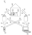
도 10은 본 개시의 양상이 유리하게 이용될 수 있는 예시적인 무선 통신 시스템(1000)을 도시하는 블록도이다. 예시의 목적으로, 도 10은 3개의 원격 유닛들(1020, 1030 및 1050) 및 2개의 기지국들(1040)을 도시한다. 무선 통신 시스템들은 많은 더 원격의 유닛들 및 기지국들을 가질 수 있음이 인식될 것이다. 원격 유닛들(1020, 1030 및 1050)은 개시된 딥 트렌치 능동 디바이스를 포함하는 IC 디바이스들(1025A,1025C 및 1025B)을 포함한다. 다른 디바이스들은 또한 기지국들, 스위칭 디바이스들 및 네트워크 장비와 같은 개시된 딥 트렌치 능동 디바이스를 포함할 수 있음이 인식될 것이다. 도 10은 기지국(1040)으로부터 원격 유닛들(1020, 1030 및 1050)로의 순방향 링크 신호들(1080) 및 원격 유닛들(1020, 1030 및 1050)로부터 기지국들(1040)로의 역방향 링크 신호들(1090)을 도시한다.[0064]
10 is a block diagram illustrating an exemplary
[0065]
도 10에서, 원격 유닛(1020)은 모바일 전화로서 도시되고, 원격 유닛(1030)은 휴대용 컴퓨터로서 도시되고, 원격 유닛(1050)은 무선 로컬 루프 시스템의 고정 위치 원격 유닛으로 도시된다. 예를 들어, 원격 유닛들은 모바일 폰, 핸드-헬드 PCS(personal communication systems) 유닛, 휴대용 데이터 유닛, 예를 들어, PDA(personal digital assistant), GPS 가능 디바이스, 내비게이션 디바이스, 셋탑 박스, 뮤직 플레이어, 비디오 플레이어, 엔터테인먼트 유닛, 고정 위치 데이터 유닛, 예를 들어, 검침(meter reading) 장비, 또는 데이터 또는 컴퓨터 명령들 또는 이들의 조합들을 저장 또는 리트리브하는 다른 통신 디바이스일 수 있다. 도 10이 본 개시의 양상들에 따른 원격 유닛들을 예시하지만, 본 개시는 이러한 예시적인 예시된 유닛들로 제한되지 않는다. 본 개시의 양상들은 개시된 딥 트렌치 능동 디바이스를 포함하는 많은 디바이스들에서 적절히 이용될 수 있다.[0065]
10, the
[0066]
도 11은 앞서 개시된 딥 트렌치 능동 디바이스와 같은 반도체 컴포넌트의 회로, 레이아웃 및 로직 설계에 사용되는 설계 워크스테이션을 예시하는 블록도이다. 설계 워크스테이션(1100)은 운영 시스템 소프트웨어, 지원 파일들 및 설계 소프트웨어, 예를 들어, Cadence 또는 OrCAD를 포함하는 하드 디스크(1101)를 포함한다. 설계 워크스테이션(1100)은 또한 회로(1110) 또는 반도체 컴포넌트(1112), 예를 들어, 딥 트렌치 능동 디바이스의 설계를 용이하게 하기 위해 디스플레이(1102)를 포함한다. 회로 설계(1110) 또는 반도체 컴포넌트(1112)를 유형으로 저장하기 위해 저장 매체(1104)가 제공된다. 회로 설계(1110) 또는 반도체 컴포넌트(1112)는 GDSII 또는 GERBER과 같은 파일 포맷으로 저장 매체(1104) 상에 저장될 수 있다. 저장 매체(1104)는 CD-ROM, DVD, 하드 디스크, 플래시 메모리 또는 다른 적절한 디바이스일 수 있다. 또한, 설계 워크스테이션(1100)은 저장 매체(1104)로부터의 입력을 수용하거나 그에 출력을 기록하기 위한 드라이브 장치(1103)를 포함한다.[0066]
Figure 11 is a block diagram illustrating a design workstation used in the circuit, layout, and logic design of semiconductor components such as the deep trench active devices disclosed above. The
[0067]
저장 매체(1104) 상에 기록된 데이터는 로직 회로 구성들, 포토리소그래피 마스크들에 대한 패턴 데이터 또는 전자 빔 리소그래피와 같은 일련의 기록 툴들에 대한 마스크 패턴 데이터를 특정할 수 있다. 데이터는 로직 시뮬레이션들과 연관된 네트 회로들 또는 타이밍 도면들과 같은 로직 검증 데이터를 더 포함할 수 있다. 저장 매체(1104) 상에 데이터를 제공하는 것은 반도체 웨이퍼들을 설계하기 위한 프로세스들의 수를 감소시킴으로써 회로 설계(1110) 또는 반도체 컴포넌트(1112)의 설계를 용이하게 한다.[0067]
The data recorded on the
[0068] 펌웨어 및/또는 소프트웨어 구현에 대해, 방법들은, 본 명세서에 설명된 기능들을 수행하는 모듈들(예를 들어, 절차들, 함수들 등)을 이용하여 구현될 수 있다. 명령들을 유형으로 구현하는 머신-판독가능 매체는 본 명세서에 설명된 방법들을 구현할 시에 사용될 수 있다. 예를 들어, 소프트웨어 코드들은 메모리에 저장될 수 있고, 프로세서 유닛에 의해 실행될 수 있다. 메모리는, 프로세서 유닛 내부 또는 프로세서 유닛 외부에서 구현될 수 있다. 본 명세서에 사용된 바와 같이, 용어 "메모리"는 장기, 단기, 휘발성, 비휘발성, 또는 다른 메모리의 타입들을 지칭하며, 메모리의 특정 타입 또는 메모리들의 수, 또는 메모리가 저장되는 매체들의 타입에 제한되지 않는다.[0068] For a firmware and / or software implementation, the methods may be implemented using modules (e.g., procedures, functions, etc.) that perform the functions described herein. A machine-readable medium implementing the instructions in a type may be used in implementing the methods described herein. For example, the software codes may be stored in memory and executed by the processor unit. The memory may be implemented within the processor unit or outside the processor unit. As used herein, the term " memory " refers to types of long, short, volatile, non-volatile, or other memory and refers to any type of memory or number of memories, It does not.
[0069] 펌웨어 및/또는 소프트웨어로 구현되면, 기능들은 컴퓨터-판독가능 매체 상의 하나 이상의 명령들 또는 코드로서 저장될 수 있다. 예들은, 데이터 구조로 인코딩된 컴퓨터-판독가능 매체들, 및 컴퓨터 프로그램으로 인코딩된 컴퓨터-판독가능 매체들을 포함한다. 컴퓨터-판독가능 매체들은 물리적 컴퓨터 저장 매체들을 포함한다. 저장 매체는 컴퓨터에 의해 액세스될 수 있는 이용가능한 매체일 수 있다. 제한이 아닌 예로서, 그러한 컴퓨터-판독가능 매체들은 RAM, ROM, EEPROM, CD-ROM 또는 다른 광학 디스크 저장부, 자기 디스크 저장 또는 다른 자기 저장 디바이스들, 또는 명령들 또는 데이터 구조들의 형태로 원하는 프로그램 코드를 저장하는데 사용될 수 있고 컴퓨터에 의해 액세스될 수 있는 다른 매체를 포함할 수 있으며; 본 명세서에 사용된 바와 같이, 디스크(disk) 및 디스크(disc)는, 컴팩트 디스크(disc)(CD), 레이저 디스크(disc), 광학 디스크(disc), DVD(digital versatile disc), 플로피 디스크(disk) 및 블루-레이 디스크(disc)를 포함하며, 여기서, 디스크(disk)들은 일반적으로 데이터를 자기적으로 재생하지만, 디스크(disc)들은 레이저들을 이용하여 광학적으로 데이터를 재생한다. 상기의 것들의 결합들이 또한 컴퓨터 판독가능 매체의 범위 내에 포함되어야 한다.[0069] When implemented in firmware and / or software, the functions may be stored as one or more instructions or code on a computer-readable medium. Examples include computer-readable media encoded with a data structure, and computer-readable media encoded with a computer program. Computer-readable media include physical computer storage media. The storage medium may be an available medium that can be accessed by a computer. By way of example, and not limitation, such computer-readable media can comprise a computer-readable medium such as RAM, ROM, EEPROM, CD-ROM or other optical disk storage, magnetic disk storage or other magnetic storage devices, May include other media that can be used to store the code and which can be accessed by a computer; As used herein, a disk and a disc may be a compact disc (CD), a laser disc, an optical disc, a digital versatile disc (DVD), a floppy disc disk and a Blu-ray disc, wherein discs generally reproduce data magnetically, while discs reproduce data optically using lasers. Combinations of the above should also be included within the scope of computer readable media.
[0070] 컴퓨터 판독가능 매체 상의 저장에 부가하여, 명령들 및/또는 데이터는 통신 장치에 포함된 송신 매체들 상에서 신호들로서 제공될 수 있다. 예를 들어, 통신 장치는, 명령들 및 데이터를 표시하는 신호들을 갖는 트랜시버를 포함할 수 있다. 명령들 및 데이터는 하나 이상의 프로세서들로 하여금, 청구항들에서 약술된 기능들을 구현하게 하도록 구성된다.[0070] In addition to storing on a computer readable medium, instructions and / or data may be provided as signals on transmission media included in a communication device. For example, the communication device may include a transceiver having signals indicative of instructions and data. The instructions and data are configured to cause one or more processors to implement the functions outlined in the claims.
[0071] 본 개시 및 이의 이점들이 상세히 설명되었지만, 첨부된 청구항들에 의해 정의된 바와 같이 본 개시의 기술로부터 벗어남이 없이 다양한 변화들, 대체들 및 변경들이 행해질 수 있음을 이해해야 한다. 예를 들어, "위" 및 "아래"와 같은 관계적 용어들이 기판 또는 전자 디바이스에 대해 사용된다. 물론, 기판 또는 전자 디바이스가 반전되면, 위는 아래가 되고, 아래는 위가 된다. 추가적으로, 측방향으로 배향되면, 위 및 아래는 기판 또는 전자 디바이스의 사이드들을 지칭할 수 있다. 또한, 본 출원의 범위는 본 명세서에 설명된 프로세스, 머신, 제조의 특정 구성들, 및 재료의 조성, 수단, 방법들 및 단계들로 제한되는 것으로 의도되지 않는다. 당업자가 본 개시로부터 쉽게 인식할 바와 같이, 본원에 설명된 대응하는 구성들과 실질적으로 동일한 결과를 달성하거나 실질적으로 동일한 기능을 수행하는, 현재 존재하는 또는 추후에 개발될 프로세스들, 머신들, 제조, 재료의 조성들, 수단, 방법들 또는 단계들이 본 개시에 따라 활용될 수 있다. 따라서, 첨부된 청구항들은 이러한 프로세스들, 머신들, 제조, 재료의 조성들, 수단, 방법들 또는 단계들을 청구항의 범위 내에 포함하는 것으로 의도된다.[0071] While this disclosure and its advantages have been described in detail, it should be understood that various changes, substitutions and alterations can be made herein without departing from the spirit of the present disclosure as defined by the appended claims. For example, relational terms such as " up " and " below " are used for the substrate or electronic device. Of course, when the substrate or electronic device is inverted, the top is down and the bottom is top. Additionally, when oriented laterally, the top and bottom may refer to the side of the substrate or electronic device. Further, the scope of the present application is not intended to be limited to the processes, machines, specific configurations of manufacture, and composition, means, methods and steps of the materials set forth herein. As those skilled in the art will readily appreciate from the present disclosure, there is no doubt that existing or later-to-be-developed processes, machines, fabrication, and the like, that achieve substantially the same results or perform substantially the same functions as the corresponding configurations described herein , Compositions of materials, means, methods, or steps may be utilized in accordance with the present disclosure. Accordingly, the appended claims are intended to cover such processes, machines, manufacture, composition of materials, means, methods, or steps within the scope of the claims.
Claims (25)
상기 복수의 게이트 핑거들과 서로 맞물리는 복수의 반도체 기둥들을 포함하는 바디;
상기 바디에 커플링된 적어도 하나의 백사이드 콘택트; 및
상기 적어도 하나의 백사이드 콘택트를 통해 상기 바디에 커플링된 백사이드 금속배선을 포함하는, 집적 회로.A gate comprising a plurality of gate fingers;
A body including a plurality of semiconductor posts interdigitated with the plurality of gate fingers;
At least one backside contact coupled to the body; And
And a backside metal interconnection coupled to the body through the at least one backside contact.
상기 복수의 게이트 핑거들은 폴리실리콘 재료를 포함하는, 집적 회로.The method according to claim 1,
Wherein the plurality of gate fingers comprise a polysilicon material.
상기 복수의 게이트 핑거들과 상기 복수의 반도체 기둥들 사이에 게이트 유전체를 더 포함하는, 집적 회로.The method according to claim 1,
And a gate dielectric between the plurality of gate fingers and the plurality of semiconductor columns.
제1 플레이트로서 상기 복수의 게이트 핑거들, 제2 플레이트로서 상기 복수의 반도체 기둥들, 및 커패시터 유전체로서 상기 게이트 유전체를 포함하는 커패시터를 더 포함하는, 집적 회로.The method of claim 3,
Further comprising the plurality of gate fingers as a first plate, the plurality of semiconductor columns as a second plate, and a capacitor comprising the gate dielectric as a capacitor dielectric.
상기 백사이드 콘택트는, 상기 바디와 상기 백사이드 금속배선 사이에 각각 커플링된 복수의 콘택트 플러그들을 포함하고, 상기 백사이드 금속배선은 상기 복수의 콘택트 플러그들에 직접 커플링되는, 집적 회로.The method according to claim 1,
Wherein the backside contact includes a plurality of contact plugs each coupled between the body and the backside metal wiring, and wherein the backside metal wiring is directly coupled to the plurality of contact plugs.
상기 백사이드 콘택트와 상기 바디 사이에 직접 백사이드 실리사이드를 더 포함하는, 집적 회로.The method according to claim 1,
Further comprising a backside silicide directly between the backside contact and the body.
상기 백사이드 실리사이드는 상기 바디 상에 직접 복수의 이산적 엘리먼트들을 포함하거나, 또는 상기 백사이드 실리사이드는 상기 바디 상에 연속적 층을 포함하는, 집적 회로.The method according to claim 6,
Wherein the backside silicide comprises a plurality of discrete elements directly on the body, or the backside silicide comprises a continuous layer on the body.
상기 게이트의 제1 사이드에 근접한 상기 바디의 제1 도핑된 영역; 및
상기 게이트의 상기 제1 사이드에 대향하는 제2 사이드에 근접한 상기 바디의 제2 도핑된 영역을 더 포함하는, 집적 회로.The method according to claim 1,
A first doped region of the body proximate a first side of the gate; And
And a second doped region of the body proximate a second side opposite the first side of the gate.
상기 제1 도핑된 영역은 소스 영역이고 상기 제2 도핑된 영역은 드레인 영역인, 집적 회로.9. The method of claim 8,
Wherein the first doped region is a source region and the second doped region is a drain region.
매립된 산화물(BOX) 층; 및
상기 매립된 산화물 층을 지지하는 백사이드 유전체 층을 더 포함하고, 상기 바디는 상기 매립된 산화물 층을 통해 확장되고 상기 백사이드 유전체 층에 의해 지지되며, 상기 백사이드 콘택트 및 상기 백사이드 금속배선은 상기 백사이드 유전체 층에 있는, 집적 회로.The method according to claim 1,
A buried oxide (BOX) layer; And
Further comprising a backside dielectric layer supporting the buried oxide layer, the body extending through the buried oxide layer and being supported by the backside dielectric layer, wherein the backside contact and the backside metal interconnection are formed on the backside dielectric layer In an integrated circuit.
매립된 산화물(BOX) 층; 및
상기 매립된 산화물 층을 지지하는 백사이드 유전체 층을 더 포함하고, 상기 바디는 상기 매립된 산화물까지 확장되고, 상기 백사이드 콘택트는 상기 바디 및 상기 백사이드 금속배선에 커플링하도록 상기 매립된 산화물 층까지 확장되는, 집적 회로.The method according to claim 1,
A buried oxide (BOX) layer; And
Further comprising a backside dielectric layer supporting the buried oxide layer, the body extending to the buried oxide and the backside contact extending to the buried oxide layer to couple to the body and the backside metal wirings , An integrated circuit.
매립된 산화물 층 ― 이를 통해 상기 게이트의 제1 부분이 확장되고, 상기 제1 부분은 상기 복수의 게이트 핑거들에 커플링됨 ―; 및
상기 매립된 산화물 층을 지지하는 백사이드 유전체 층을 더 포함하는, 집적 회로.The method according to claim 1,
A buried oxide layer through which a first portion of the gate is extended and the first portion is coupled to the plurality of gate fingers; And
And a backside dielectric layer to support the buried oxide layer.
RF(radio frequency) 프론트 엔드 모듈에 통합되며, 상기 RF 프론트 엔드 모듈은 뮤직 플레이어, 비디오 플레이어, 엔터테인먼트 유닛, 내비게이션 디바이스, 통신 디바이스, PDA(personal digital assistant), 고정 위치 데이터 유닛, 모바일 폰 및 휴대용 컴퓨터 중 적어도 하나에 통합되는, 집적 회로.The method according to claim 1,
The RF front end module is integrated into a radio frequency (RF) front end module, which may be a music player, a video player, an entertainment unit, a navigation device, a communication device, a personal digital assistant (PDA), a fixed location data unit, RTI ID = 0.0 > 1, < / RTI >
상기 절연 층의 프론트-사이드 표면 상에 및 상기 복수의 반도체 기둥들의 표면 상에 유전체 재료 층을 증착하는 단계;
복수의 게이트 핑거들을 포함하는 게이트를 형성하기 위해 상기 유전체 재료 층 상에 및 상기 복수의 반도체 기둥들을 분리하는 복수의 트렌치들에 반도체 재료를 증착하는 단계 ― 상기 복수의 게이트 핑거들은 상기 복수의 반도체 기둥들과 서로 맞물림 ―;
상기 절연 층의 상기 프론트-사이드 표면 상의 프론트-사이드 유전체 층에 핸들 기판을 본딩하는 단계; 및
상기 절연 층의 백사이드 표면을 지지하는 백사이드 유전체 층에 백사이드 금속배선을 제조하는 단계를 포함하고, 상기 백사이드 금속배선은 적어도 하나의 백사이드 콘택트를 통해 상기 바디에 커플링되는, 집적 회로를 구성하는 방법.Etching a semiconductor layer in an insulating layer to form a body including a plurality of semiconductor posts;
Depositing a dielectric material layer on the front-side surface of the insulating layer and on the surface of the plurality of semiconductor columns;
Depositing a semiconductor material on the dielectric material layer and on a plurality of trenches separating the plurality of semiconductor columns to form a gate comprising a plurality of gate fingers, - engage with each other;
Bonding a handle substrate to a front-side dielectric layer on the front-side surface of the insulating layer; And
Fabricating a backside metal interconnection in a backside dielectric layer that supports a backside surface of the insulating layer, wherein the backside metal interconnection is coupled to the body through at least one backside contact.
상기 반도체 재료를 증착하는 단계는, 상기 복수의 게이트 핑거들을 포함하는 게이트를 형성하기 위해 상기 유전체 재료 층 상에 및 상기 복수의 반도체 기둥들을 분리하는 상기 복수의 트렌치들에 폴리실리콘 재료를 증착하는 단계를 포함하는, 집적 회로를 구성하는 방법.15. The method of claim 14,
Depositing a polysilicon material on the dielectric material layer and the plurality of trenches separating the plurality of semiconductor columns to form a gate comprising the plurality of gate fingers, ≪ / RTI >
상기 백사이드 콘택트와 상기 바디 사이에 직접 백사이드 실리사이드를 증착하는 단계를 더 포함하는, 집적 회로를 구성하는 방법.15. The method of claim 14,
Depositing a backside silicide directly between the backside contact and the body. ≪ RTI ID = 0.0 > 31. < / RTI >
상기 백사이드 실리사이드를 복수의 이산적 엘리먼트들로서, 상기 바디 상에 직접 또는 상기 바디 상에 연속적 층으로서 증착하는 단계를 더 포함하는, 집적 회로를 구성하는 방법.17. The method of claim 16,
Depositing the backside suicide as a plurality of discrete elements, either directly on the body or as a continuous layer on the body.
상기 게이트의 제1 사이드에 근접한 상기 바디의 제1 도핑된 영역을 도핑하는 단계; 및
상기 게이트의 상기 제1 사이드에 대향하는 제2 사이드에 근접한 상기 바디의 제2 도핑된 영역을 도핑하는 단계를 더 포함하는, 집적 회로를 구성하는 방법.15. The method of claim 14,
Doping a first doped region of the body proximate a first side of the gate; And
Further comprising doping a second doped region of the body proximate a second side opposite the first side of the gate.
상기 반도체 재료를 증착하는 단계는 매립된 산화물 층을 통해 확장되는 상기 게이트의 제1 부분을 증착하는 단계를 더 포함하고, 상기 게이트의 제1 부분은 상기 복수의 게이트 핑거들에 커플링되는, 집적 회로를 구성하는 방법.15. The method of claim 14,
Wherein depositing the semiconductor material further comprises depositing a first portion of the gate extending through the buried oxide layer and wherein a first portion of the gate is coupled to the plurality of gate fingers, Method of constructing a circuit.
상기 집적 회로를 RF(radio frequency) 프론트 엔드 모듈에 집적하는 단계를 더 포함하고, 상기 RF 프론트 엔드 모듈은 뮤직 플레이어, 비디오 플레이어, 엔터테인먼트 유닛, 내비게이션 디바이스, 통신 디바이스, PDA(personal digital assistant), 고정 위치 데이터 유닛, 모바일 폰 및 휴대용 컴퓨터 중 적어도 하나에 통합되는, 집적 회로를 구성하는 방법.15. The method of claim 14,
Further comprising integrating the integrated circuit into a radio frequency (RF) front end module, wherein the RF front end module is a music player, a video player, an entertainment unit, a navigation device, a communication device, a personal digital assistant (PDA) Location data unit, a mobile phone, and a portable computer.
상기 복수의 게이트 핑거들과 서로 맞물리는 복수의 반도체 기둥들을 포함하는 바디;
상기 바디에 커플링된 적어도 하나의 백사이드 콘택트; 및
상기 적어도 하나의 백사이드 콘택트를 통해 상기 바디를 연결하기 위한 수단을 포함하는, 집적 회로.A gate comprising a plurality of gate fingers;
A body including a plurality of semiconductor posts interdigitated with the plurality of gate fingers;
At least one backside contact coupled to the body; And
And means for connecting the body through the at least one backside contact.
상기 게이트의 제1 사이드에 근접한 상기 바디의 제1 도핑된 영역; 및
상기 게이트의 상기 제1 사이드에 대향하는 제2 사이드에 근접한 상기 바디의 제2 도핑된 영역을 더 포함하는, 집적 회로.22. The method of claim 21,
A first doped region of the body proximate a first side of the gate; And
And a second doped region of the body proximate a second side opposite the first side of the gate.
RF(radio frequency) 프론트 엔드 모듈에 통합되며, 상기 RF 프론트 엔드 모듈은 뮤직 플레이어, 비디오 플레이어, 엔터테인먼트 유닛, 내비게이션 디바이스, 통신 디바이스, PDA(personal digital assistant), 고정 위치 데이터 유닛, 모바일 폰 및 휴대용 컴퓨터 중 적어도 하나에 통합되는, 집적 회로.22. The method of claim 21,
The RF front end module is integrated into a radio frequency (RF) front end module, which may be a music player, a video player, an entertainment unit, a navigation device, a communication device, a personal digital assistant (PDA), a fixed location data unit, RTI ID = 0.0 > 1, < / RTI >
상기 스위치 트랜지스터의 출력에 커플링되는 안테나를 포함하는, RF 프론트 엔드 모듈.A deep trench switch transistor including a body including a gate including a plurality of gate fingers and a plurality of semiconductor posts engaged with the plurality of gate fingers, at least one backside contact coupled to the body, An integrated radio frequency circuit including a backside metal wire coupled to the body through one backside contact; And
And an antenna coupled to an output of the switch transistor.
뮤직 플레이어, 비디오 플레이어, 엔터테인먼트 유닛, 내비게이션 디바이스, 통신 디바이스, PDA(personal digital assistant), 고정 위치 데이터 유닛, 모바일 폰 및 휴대용 컴퓨터 중 적어도 하나에 통합되는, RF 프론트 엔드 모듈.25. The method of claim 24,
Wherein the integrated circuit is integrated into at least one of a music player, a video player, an entertainment unit, a navigation device, a communication device, a personal digital assistant (PDA), a fixed location data unit, a mobile phone and a portable computer.
Applications Claiming Priority (3)
| Application Number | Priority Date | Filing Date | Title |
|---|---|---|---|
| US15/257,823 US9812580B1 (en) | 2016-09-06 | 2016-09-06 | Deep trench active device with backside body contact |
| US15/257,823 | 2016-09-06 | ||
| PCT/US2017/045349 WO2018048529A1 (en) | 2016-09-06 | 2017-08-03 | Deep trench active device with backside body contact |
Publications (1)
| Publication Number | Publication Date |
|---|---|
| KR20190045909A true KR20190045909A (en) | 2019-05-03 |
Family
ID=59684050
Family Applications (1)
| Application Number | Title | Priority Date | Filing Date |
|---|---|---|---|
| KR1020197006280A KR20190045909A (en) | 2016-09-06 | 2017-08-03 | Deep trench active devices with backside body contacts |
Country Status (7)
| Country | Link |
|---|---|
| US (1) | US9812580B1 (en) |
| EP (1) | EP3510636A1 (en) |
| JP (1) | JP2019530218A (en) |
| KR (1) | KR20190045909A (en) |
| CN (1) | CN109791948A (en) |
| BR (1) | BR112019003900A2 (en) |
| WO (1) | WO2018048529A1 (en) |
Cited By (1)
| Publication number | Priority date | Publication date | Assignee | Title |
|---|---|---|---|---|
| KR20210148843A (en) * | 2020-05-28 | 2021-12-08 | 타이완 세미콘덕터 매뉴팩쳐링 컴퍼니 리미티드 | Semiconductor device with air gaps and method of fabrication thereof |
Families Citing this family (13)
| Publication number | Priority date | Publication date | Assignee | Title |
|---|---|---|---|---|
| CN110504240B (en) * | 2018-05-16 | 2021-08-13 | 联华电子股份有限公司 | Semiconductor device and method for manufacturing the same |
| CN109524355B (en) * | 2018-10-30 | 2020-11-10 | 上海集成电路研发中心有限公司 | Structure and forming method of semiconductor device |
| CN109545785B (en) * | 2018-10-31 | 2023-01-31 | 上海集成电路研发中心有限公司 | Semiconductor device structure and preparation method |
| CN109616472B (en) * | 2018-12-14 | 2022-11-15 | 上海微阱电子科技有限公司 | Semiconductor device structure and forming method |
| CN109545802B (en) * | 2018-12-14 | 2021-01-12 | 上海微阱电子科技有限公司 | Semiconductor-on-insulator device structure and forming method |
| KR102635376B1 (en) * | 2019-01-30 | 2024-02-07 | 양쯔 메모리 테크놀로지스 씨오., 엘티디. | Capacitor structure with vertical diffuser plate |
| WO2020154950A1 (en) * | 2019-01-30 | 2020-08-06 | Yangtze Memory Technologies Co., Ltd. | Capacitor structure having vertical diffusion plates |
| EP3853896A4 (en) * | 2019-02-18 | 2022-06-08 | Yangtze Memory Technologies Co., Ltd. | Novel capacitor structure and method of forming the same |
| US11355410B2 (en) * | 2020-04-28 | 2022-06-07 | Taiwan Semiconductor Manufacturing Co., Ltd. | Thermal dissipation in semiconductor devices |
| DE102020122151A1 (en) * | 2020-04-28 | 2021-10-28 | Taiwan Semiconductor Manufacturing Co., Ltd. | SEMICONDUCTOR DEVICE AND METHOD |
| TWI741935B (en) | 2020-04-28 | 2021-10-01 | 台灣積體電路製造股份有限公司 | Semiconductor devices and method of forming the same |
| US11251308B2 (en) | 2020-04-28 | 2022-02-15 | Taiwan Semiconductor Manufacturing Co., Ltd. | Semiconductor device and method |
| US11349004B2 (en) * | 2020-04-28 | 2022-05-31 | Taiwan Semiconductor Manufacturing Co., Ltd. | Backside vias in semiconductor device |
Family Cites Families (19)
| Publication number | Priority date | Publication date | Assignee | Title |
|---|---|---|---|---|
| JP2948018B2 (en) * | 1992-03-17 | 1999-09-13 | 三菱電機株式会社 | Semiconductor device and manufacturing method thereof |
| US5889298A (en) | 1993-04-30 | 1999-03-30 | Texas Instruments Incorporated | Vertical JFET field effect transistor |
| JP3884266B2 (en) * | 2001-02-19 | 2007-02-21 | 株式会社東芝 | Semiconductor memory device and manufacturing method thereof |
| US6838722B2 (en) | 2002-03-22 | 2005-01-04 | Siliconix Incorporated | Structures of and methods of fabricating trench-gated MIS devices |
| JP2003309182A (en) * | 2002-04-17 | 2003-10-31 | Hitachi Ltd | Method of manufacturing semiconductor device and semiconductor device |
| US6861701B2 (en) | 2003-03-05 | 2005-03-01 | Advanced Analogic Technologies, Inc. | Trench power MOSFET with planarized gate bus |
| JP4869546B2 (en) * | 2003-05-23 | 2012-02-08 | ルネサスエレクトロニクス株式会社 | Semiconductor device |
| JP2005353657A (en) * | 2004-06-08 | 2005-12-22 | Matsushita Electric Ind Co Ltd | Semiconductor device and its manufacturing method |
| DE102005030585B4 (en) * | 2005-06-30 | 2011-07-28 | Globalfoundries Inc. | Semiconductor device with a vertical decoupling capacitor and method for its production |
| JP2009088241A (en) * | 2007-09-28 | 2009-04-23 | Renesas Technology Corp | Semiconductor device and manufacturing method thereof |
| JP5487625B2 (en) * | 2009-01-22 | 2014-05-07 | ソニー株式会社 | Semiconductor device |
| US8395880B2 (en) * | 2010-03-30 | 2013-03-12 | Medtronic, Inc. | High density capacitor array patterns |
| US8735984B2 (en) * | 2010-07-06 | 2014-05-27 | Globalfoundries Singapore PTE, LTD. | FinFET with novel body contact for multiple Vt applications |
| US9159825B2 (en) | 2010-10-12 | 2015-10-13 | Silanna Semiconductor U.S.A., Inc. | Double-sided vertical semiconductor device with thinned substrate |
| US9496255B2 (en) * | 2011-11-16 | 2016-11-15 | Qualcomm Incorporated | Stacked CMOS chipset having an insulating layer and a secondary layer and method of forming same |
| US8735993B2 (en) * | 2012-01-31 | 2014-05-27 | Taiwan Semiconductor Manufacturing Company, Ltd. | FinFET body contact and method of making same |
| US20160172527A1 (en) * | 2012-12-03 | 2016-06-16 | Sandia Corporation | Photodetector with Interdigitated Nanoelectrode Grating Antenna |
| US9478507B2 (en) * | 2013-03-27 | 2016-10-25 | Qualcomm Incorporated | Integrated circuit assembly with faraday cage |
| US8748245B1 (en) | 2013-03-27 | 2014-06-10 | Io Semiconductor, Inc. | Semiconductor-on-insulator integrated circuit with interconnect below the insulator |
-
2016
- 2016-09-06 US US15/257,823 patent/US9812580B1/en active Active
-
2017
- 2017-08-03 KR KR1020197006280A patent/KR20190045909A/en not_active Application Discontinuation
- 2017-08-03 CN CN201780054488.8A patent/CN109791948A/en active Pending
- 2017-08-03 WO PCT/US2017/045349 patent/WO2018048529A1/en active Search and Examination
- 2017-08-03 JP JP2019512208A patent/JP2019530218A/en active Pending
- 2017-08-03 BR BR112019003900-7A patent/BR112019003900A2/en not_active IP Right Cessation
- 2017-08-03 EP EP17755340.1A patent/EP3510636A1/en not_active Withdrawn
Cited By (2)
| Publication number | Priority date | Publication date | Assignee | Title |
|---|---|---|---|---|
| KR20210148843A (en) * | 2020-05-28 | 2021-12-08 | 타이완 세미콘덕터 매뉴팩쳐링 컴퍼니 리미티드 | Semiconductor device with air gaps and method of fabrication thereof |
| US11830769B2 (en) | 2020-05-28 | 2023-11-28 | Taiwan Semiconductor Manufacturing Co., Ltd. | Semiconductor device with air gaps and method of fabrication thereof |
Also Published As
| Publication number | Publication date |
|---|---|
| JP2019530218A (en) | 2019-10-17 |
| EP3510636A1 (en) | 2019-07-17 |
| BR112019003900A2 (en) | 2019-05-21 |
| CN109791948A (en) | 2019-05-21 |
| US9812580B1 (en) | 2017-11-07 |
| WO2018048529A1 (en) | 2018-03-15 |
Similar Documents
| Publication | Publication Date | Title |
|---|---|---|
| KR102054924B1 (en) | Logic Circuit Block Layouts with Dual-Side Processing | |
| US9812580B1 (en) | Deep trench active device with backside body contact | |
| EP3449503B1 (en) | Integrated radio frequency circuit structure | |
| CN109643691B (en) | Backside semiconductor growth | |
| EP3443592B1 (en) | Switch device performance improvement through multisided biased shielding | |
| CN111133565B (en) | Bulk layer transfer process using backside silicidation | |
| US9917062B1 (en) | Self-aligned transistors for dual-side processing | |
| US20180068886A1 (en) | Porous semiconductor layer transfer for an integrated circuit structure | |
| US10043752B2 (en) | Substrate contact using dual sided silicidation | |
| US10290579B2 (en) | Utilization of backside silicidation to form dual side contacted capacitor |
Legal Events
| Date | Code | Title | Description |
|---|---|---|---|
| A201 | Request for examination | ||
| E902 | Notification of reason for refusal | ||
| E601 | Decision to refuse application |