JP2019530218A - Deep trench active device with back body contact - Google Patents
Deep trench active device with back body contact Download PDFInfo
- Publication number
- JP2019530218A JP2019530218A JP2019512208A JP2019512208A JP2019530218A JP 2019530218 A JP2019530218 A JP 2019530218A JP 2019512208 A JP2019512208 A JP 2019512208A JP 2019512208 A JP2019512208 A JP 2019512208A JP 2019530218 A JP2019530218 A JP 2019530218A
- Authority
- JP
- Japan
- Prior art keywords
- gate
- integrated circuit
- layer
- backside
- coupled
- Prior art date
- Legal status (The legal status is an assumption and is not a legal conclusion. Google has not performed a legal analysis and makes no representation as to the accuracy of the status listed.)
- Pending
Links
- 239000004065 semiconductor Substances 0.000 claims abstract description 64
- 238000001465 metallisation Methods 0.000 claims abstract description 33
- 238000000034 method Methods 0.000 claims description 95
- 239000000758 substrate Substances 0.000 claims description 59
- 239000003990 capacitor Substances 0.000 claims description 26
- 238000004891 communication Methods 0.000 claims description 14
- 229910021332 silicide Inorganic materials 0.000 claims description 13
- FVBUAEGBCNSCDD-UHFFFAOYSA-N silicide(4-) Chemical compound [Si-4] FVBUAEGBCNSCDD-UHFFFAOYSA-N 0.000 claims description 13
- 239000003989 dielectric material Substances 0.000 claims description 12
- 238000000151 deposition Methods 0.000 claims description 11
- 239000000463 material Substances 0.000 claims description 11
- 238000000576 coating method Methods 0.000 claims description 8
- 239000002184 metal Substances 0.000 claims description 8
- 239000011248 coating agent Substances 0.000 claims description 7
- 238000005530 etching Methods 0.000 claims description 3
- 229910021420 polycrystalline silicon Inorganic materials 0.000 claims description 3
- 229920005591 polysilicon Polymers 0.000 claims description 3
- 230000008569 process Effects 0.000 description 70
- 238000012546 transfer Methods 0.000 description 30
- 238000013461 design Methods 0.000 description 25
- 238000007667 floating Methods 0.000 description 25
- XUIMIQQOPSSXEZ-UHFFFAOYSA-N Silicon Chemical compound [Si] XUIMIQQOPSSXEZ-UHFFFAOYSA-N 0.000 description 24
- 230000000694 effects Effects 0.000 description 24
- 229910052710 silicon Inorganic materials 0.000 description 24
- 239000010703 silicon Substances 0.000 description 24
- 239000012212 insulator Substances 0.000 description 21
- 238000010586 diagram Methods 0.000 description 16
- 238000003860 storage Methods 0.000 description 14
- 230000003071 parasitic effect Effects 0.000 description 12
- 230000006870 function Effects 0.000 description 11
- 238000005516 engineering process Methods 0.000 description 10
- 230000015654 memory Effects 0.000 description 10
- 238000004519 manufacturing process Methods 0.000 description 9
- 230000015572 biosynthetic process Effects 0.000 description 6
- 238000004220 aggregation Methods 0.000 description 5
- 230000002776 aggregation Effects 0.000 description 5
- 230000001154 acute effect Effects 0.000 description 3
- 230000008878 coupling Effects 0.000 description 3
- 238000010168 coupling process Methods 0.000 description 3
- 238000005859 coupling reaction Methods 0.000 description 3
- 238000009413 insulation Methods 0.000 description 3
- 229910044991 metal oxide Inorganic materials 0.000 description 3
- 150000004706 metal oxides Chemical class 0.000 description 3
- 239000000203 mixture Substances 0.000 description 3
- 239000000615 nonconductor Substances 0.000 description 3
- 230000002411 adverse Effects 0.000 description 2
- 238000000231 atomic layer deposition Methods 0.000 description 2
- 230000005540 biological transmission Effects 0.000 description 2
- 238000005229 chemical vapour deposition Methods 0.000 description 2
- 238000002955 isolation Methods 0.000 description 2
- 230000003287 optical effect Effects 0.000 description 2
- 230000002441 reversible effect Effects 0.000 description 2
- 101100154785 Mus musculus Tulp2 gene Proteins 0.000 description 1
- 239000003570 air Substances 0.000 description 1
- 238000000137 annealing Methods 0.000 description 1
- 235000013405 beer Nutrition 0.000 description 1
- 230000000295 complement effect Effects 0.000 description 1
- 238000004590 computer program Methods 0.000 description 1
- 238000010276 construction Methods 0.000 description 1
- 238000000609 electron-beam lithography Methods 0.000 description 1
- 238000000407 epitaxy Methods 0.000 description 1
- 238000001914 filtration Methods 0.000 description 1
- 239000011521 glass Substances 0.000 description 1
- 238000002513 implantation Methods 0.000 description 1
- 238000003780 insertion Methods 0.000 description 1
- 230000037431 insertion Effects 0.000 description 1
- 238000005468 ion implantation Methods 0.000 description 1
- 238000005304 joining Methods 0.000 description 1
- 230000007787 long-term memory Effects 0.000 description 1
- 239000012528 membrane Substances 0.000 description 1
- 238000012986 modification Methods 0.000 description 1
- 230000004048 modification Effects 0.000 description 1
- 238000005457 optimization Methods 0.000 description 1
- 230000003647 oxidation Effects 0.000 description 1
- 238000007254 oxidation reaction Methods 0.000 description 1
- 238000002161 passivation Methods 0.000 description 1
- 238000000206 photolithography Methods 0.000 description 1
- 238000005498 polishing Methods 0.000 description 1
- 239000010453 quartz Substances 0.000 description 1
- 230000004044 response Effects 0.000 description 1
- 229910052594 sapphire Inorganic materials 0.000 description 1
- 239000010980 sapphire Substances 0.000 description 1
- 238000000926 separation method Methods 0.000 description 1
- 230000006403 short-term memory Effects 0.000 description 1
- VYPSYNLAJGMNEJ-UHFFFAOYSA-N silicon dioxide Inorganic materials O=[Si]=O VYPSYNLAJGMNEJ-UHFFFAOYSA-N 0.000 description 1
- 238000004088 simulation Methods 0.000 description 1
- 239000000126 substance Substances 0.000 description 1
- 238000006467 substitution reaction Methods 0.000 description 1
- 238000012795 verification Methods 0.000 description 1
Images


Classifications
-
- H—ELECTRICITY
- H01—ELECTRIC ELEMENTS
- H01L—SEMICONDUCTOR DEVICES NOT COVERED BY CLASS H10
- H01L29/00—Semiconductor devices specially adapted for rectifying, amplifying, oscillating or switching and having potential barriers; Capacitors or resistors having potential barriers, e.g. a PN-junction depletion layer or carrier concentration layer; Details of semiconductor bodies or of electrodes thereof ; Multistep manufacturing processes therefor
- H01L29/66—Types of semiconductor device ; Multistep manufacturing processes therefor
- H01L29/68—Types of semiconductor device ; Multistep manufacturing processes therefor controllable by only the electric current supplied, or only the electric potential applied, to an electrode which does not carry the current to be rectified, amplified or switched
- H01L29/76—Unipolar devices, e.g. field effect transistors
- H01L29/772—Field effect transistors
- H01L29/78—Field effect transistors with field effect produced by an insulated gate
- H01L29/786—Thin film transistors, i.e. transistors with a channel being at least partly a thin film
- H01L29/78606—Thin film transistors, i.e. transistors with a channel being at least partly a thin film with supplementary region or layer in the thin film or in the insulated bulk substrate supporting it for controlling or increasing the safety of the device
- H01L29/78612—Thin film transistors, i.e. transistors with a channel being at least partly a thin film with supplementary region or layer in the thin film or in the insulated bulk substrate supporting it for controlling or increasing the safety of the device for preventing the kink- or the snapback effect, e.g. discharging the minority carriers of the channel region for preventing bipolar effect
- H01L29/78615—Thin film transistors, i.e. transistors with a channel being at least partly a thin film with supplementary region or layer in the thin film or in the insulated bulk substrate supporting it for controlling or increasing the safety of the device for preventing the kink- or the snapback effect, e.g. discharging the minority carriers of the channel region for preventing bipolar effect with a body contact
-
- H—ELECTRICITY
- H01—ELECTRIC ELEMENTS
- H01L—SEMICONDUCTOR DEVICES NOT COVERED BY CLASS H10
- H01L21/00—Processes or apparatus adapted for the manufacture or treatment of semiconductor or solid state devices or of parts thereof
- H01L21/70—Manufacture or treatment of devices consisting of a plurality of solid state components formed in or on a common substrate or of parts thereof; Manufacture of integrated circuit devices or of parts thereof
- H01L21/71—Manufacture of specific parts of devices defined in group H01L21/70
- H01L21/76—Making of isolation regions between components
- H01L21/762—Dielectric regions, e.g. EPIC dielectric isolation, LOCOS; Trench refilling techniques, SOI technology, use of channel stoppers
- H01L21/7624—Dielectric regions, e.g. EPIC dielectric isolation, LOCOS; Trench refilling techniques, SOI technology, use of channel stoppers using semiconductor on insulator [SOI] technology
- H01L21/76251—Dielectric regions, e.g. EPIC dielectric isolation, LOCOS; Trench refilling techniques, SOI technology, use of channel stoppers using semiconductor on insulator [SOI] technology using bonding techniques
-
- H—ELECTRICITY
- H01—ELECTRIC ELEMENTS
- H01L—SEMICONDUCTOR DEVICES NOT COVERED BY CLASS H10
- H01L23/00—Details of semiconductor or other solid state devices
- H01L23/48—Arrangements for conducting electric current to or from the solid state body in operation, e.g. leads, terminal arrangements ; Selection of materials therefor
- H01L23/481—Internal lead connections, e.g. via connections, feedthrough structures
-
- H—ELECTRICITY
- H01—ELECTRIC ELEMENTS
- H01L—SEMICONDUCTOR DEVICES NOT COVERED BY CLASS H10
- H01L23/00—Details of semiconductor or other solid state devices
- H01L23/52—Arrangements for conducting electric current within the device in operation from one component to another, i.e. interconnections, e.g. wires, lead frames
- H01L23/522—Arrangements for conducting electric current within the device in operation from one component to another, i.e. interconnections, e.g. wires, lead frames including external interconnections consisting of a multilayer structure of conductive and insulating layers inseparably formed on the semiconductor body
- H01L23/5222—Capacitive arrangements or effects of, or between wiring layers
- H01L23/5223—Capacitor integral with wiring layers
-
- H—ELECTRICITY
- H01—ELECTRIC ELEMENTS
- H01L—SEMICONDUCTOR DEVICES NOT COVERED BY CLASS H10
- H01L23/00—Details of semiconductor or other solid state devices
- H01L23/58—Structural electrical arrangements for semiconductor devices not otherwise provided for, e.g. in combination with batteries
- H01L23/64—Impedance arrangements
- H01L23/66—High-frequency adaptations
-
- H—ELECTRICITY
- H01—ELECTRIC ELEMENTS
- H01L—SEMICONDUCTOR DEVICES NOT COVERED BY CLASS H10
- H01L27/00—Devices consisting of a plurality of semiconductor or other solid-state components formed in or on a common substrate
- H01L27/02—Devices consisting of a plurality of semiconductor or other solid-state components formed in or on a common substrate including semiconductor components specially adapted for rectifying, oscillating, amplifying or switching and having potential barriers; including integrated passive circuit elements having potential barriers
- H01L27/12—Devices consisting of a plurality of semiconductor or other solid-state components formed in or on a common substrate including semiconductor components specially adapted for rectifying, oscillating, amplifying or switching and having potential barriers; including integrated passive circuit elements having potential barriers the substrate being other than a semiconductor body, e.g. an insulating body
- H01L27/1203—Devices consisting of a plurality of semiconductor or other solid-state components formed in or on a common substrate including semiconductor components specially adapted for rectifying, oscillating, amplifying or switching and having potential barriers; including integrated passive circuit elements having potential barriers the substrate being other than a semiconductor body, e.g. an insulating body the substrate comprising an insulating body on a semiconductor body, e.g. SOI
- H01L27/1211—Devices consisting of a plurality of semiconductor or other solid-state components formed in or on a common substrate including semiconductor components specially adapted for rectifying, oscillating, amplifying or switching and having potential barriers; including integrated passive circuit elements having potential barriers the substrate being other than a semiconductor body, e.g. an insulating body the substrate comprising an insulating body on a semiconductor body, e.g. SOI combined with field-effect transistors with a horizontal current flow in a vertical sidewall of a semiconductor body, e.g. FinFET, MuGFET
-
- H—ELECTRICITY
- H01—ELECTRIC ELEMENTS
- H01L—SEMICONDUCTOR DEVICES NOT COVERED BY CLASS H10
- H01L29/00—Semiconductor devices specially adapted for rectifying, amplifying, oscillating or switching and having potential barriers; Capacitors or resistors having potential barriers, e.g. a PN-junction depletion layer or carrier concentration layer; Details of semiconductor bodies or of electrodes thereof ; Multistep manufacturing processes therefor
- H01L29/02—Semiconductor bodies ; Multistep manufacturing processes therefor
- H01L29/06—Semiconductor bodies ; Multistep manufacturing processes therefor characterised by their shape; characterised by the shapes, relative sizes, or dispositions of the semiconductor regions ; characterised by the concentration or distribution of impurities within semiconductor regions
- H01L29/0603—Semiconductor bodies ; Multistep manufacturing processes therefor characterised by their shape; characterised by the shapes, relative sizes, or dispositions of the semiconductor regions ; characterised by the concentration or distribution of impurities within semiconductor regions characterised by particular constructional design considerations, e.g. for preventing surface leakage, for controlling electric field concentration or for internal isolations regions
- H01L29/0642—Isolation within the component, i.e. internal isolation
- H01L29/0649—Dielectric regions, e.g. SiO2 regions, air gaps
-
- H—ELECTRICITY
- H01—ELECTRIC ELEMENTS
- H01L—SEMICONDUCTOR DEVICES NOT COVERED BY CLASS H10
- H01L29/00—Semiconductor devices specially adapted for rectifying, amplifying, oscillating or switching and having potential barriers; Capacitors or resistors having potential barriers, e.g. a PN-junction depletion layer or carrier concentration layer; Details of semiconductor bodies or of electrodes thereof ; Multistep manufacturing processes therefor
- H01L29/66—Types of semiconductor device ; Multistep manufacturing processes therefor
- H01L29/66007—Multistep manufacturing processes
- H01L29/66075—Multistep manufacturing processes of devices having semiconductor bodies comprising group 14 or group 13/15 materials
- H01L29/66227—Multistep manufacturing processes of devices having semiconductor bodies comprising group 14 or group 13/15 materials the devices being controllable only by the electric current supplied or the electric potential applied, to an electrode which does not carry the current to be rectified, amplified or switched, e.g. three-terminal devices
- H01L29/66409—Unipolar field-effect transistors
- H01L29/66477—Unipolar field-effect transistors with an insulated gate, i.e. MISFET
- H01L29/66787—Unipolar field-effect transistors with an insulated gate, i.e. MISFET with a gate at the side of the channel
- H01L29/66795—Unipolar field-effect transistors with an insulated gate, i.e. MISFET with a gate at the side of the channel with a horizontal current flow in a vertical sidewall of a semiconductor body, e.g. FinFET, MuGFET
-
- H—ELECTRICITY
- H01—ELECTRIC ELEMENTS
- H01L—SEMICONDUCTOR DEVICES NOT COVERED BY CLASS H10
- H01L29/00—Semiconductor devices specially adapted for rectifying, amplifying, oscillating or switching and having potential barriers; Capacitors or resistors having potential barriers, e.g. a PN-junction depletion layer or carrier concentration layer; Details of semiconductor bodies or of electrodes thereof ; Multistep manufacturing processes therefor
- H01L29/66—Types of semiconductor device ; Multistep manufacturing processes therefor
- H01L29/68—Types of semiconductor device ; Multistep manufacturing processes therefor controllable by only the electric current supplied, or only the electric potential applied, to an electrode which does not carry the current to be rectified, amplified or switched
- H01L29/76—Unipolar devices, e.g. field effect transistors
- H01L29/772—Field effect transistors
- H01L29/78—Field effect transistors with field effect produced by an insulated gate
- H01L29/785—Field effect transistors with field effect produced by an insulated gate having a channel with a horizontal current flow in a vertical sidewall of a semiconductor body, e.g. FinFET, MuGFET
- H01L29/7851—Field effect transistors with field effect produced by an insulated gate having a channel with a horizontal current flow in a vertical sidewall of a semiconductor body, e.g. FinFET, MuGFET with the body tied to the substrate
-
- H—ELECTRICITY
- H01—ELECTRIC ELEMENTS
- H01Q—ANTENNAS, i.e. RADIO AERIALS
- H01Q1/00—Details of, or arrangements associated with, antennas
- H01Q1/12—Supports; Mounting means
- H01Q1/22—Supports; Mounting means by structural association with other equipment or articles
- H01Q1/24—Supports; Mounting means by structural association with other equipment or articles with receiving set
- H01Q1/241—Supports; Mounting means by structural association with other equipment or articles with receiving set used in mobile communications, e.g. GSM
-
- H—ELECTRICITY
- H01—ELECTRIC ELEMENTS
- H01Q—ANTENNAS, i.e. RADIO AERIALS
- H01Q1/00—Details of, or arrangements associated with, antennas
- H01Q1/36—Structural form of radiating elements, e.g. cone, spiral, umbrella; Particular materials used therewith
- H01Q1/38—Structural form of radiating elements, e.g. cone, spiral, umbrella; Particular materials used therewith formed by a conductive layer on an insulating support
-
- H—ELECTRICITY
- H01—ELECTRIC ELEMENTS
- H01L—SEMICONDUCTOR DEVICES NOT COVERED BY CLASS H10
- H01L2223/00—Details relating to semiconductor or other solid state devices covered by the group H01L23/00
- H01L2223/58—Structural electrical arrangements for semiconductor devices not otherwise provided for
- H01L2223/64—Impedance arrangements
- H01L2223/66—High-frequency adaptations
- H01L2223/6605—High-frequency electrical connections
- H01L2223/6616—Vertical connections, e.g. vias
-
- H—ELECTRICITY
- H01—ELECTRIC ELEMENTS
- H01L—SEMICONDUCTOR DEVICES NOT COVERED BY CLASS H10
- H01L2223/00—Details relating to semiconductor or other solid state devices covered by the group H01L23/00
- H01L2223/58—Structural electrical arrangements for semiconductor devices not otherwise provided for
- H01L2223/64—Impedance arrangements
- H01L2223/66—High-frequency adaptations
- H01L2223/6661—High-frequency adaptations for passive devices
- H01L2223/6677—High-frequency adaptations for passive devices for antenna, e.g. antenna included within housing of semiconductor device
Landscapes
- Engineering & Computer Science (AREA)
- Power Engineering (AREA)
- Microelectronics & Electronic Packaging (AREA)
- Physics & Mathematics (AREA)
- Condensed Matter Physics & Semiconductors (AREA)
- General Physics & Mathematics (AREA)
- Computer Hardware Design (AREA)
- Ceramic Engineering (AREA)
- Manufacturing & Machinery (AREA)
- Computer Networks & Wireless Communication (AREA)
- Metal-Oxide And Bipolar Metal-Oxide Semiconductor Integrated Circuits (AREA)
- Thin Film Transistor (AREA)
- Semiconductor Integrated Circuits (AREA)
- Junction Field-Effect Transistors (AREA)
- Electrodes Of Semiconductors (AREA)
- Internal Circuitry In Semiconductor Integrated Circuit Devices (AREA)
Abstract
集積回路は、ゲートフィンガーを有するゲートを含み得る。集積回路はまた、ゲートのゲートフィンガーとインターロックする半導体ピラーを有するボディを含み得る。集積回路はまた、ボディに結合された裏面接点を含み得る。集積回路は、裏面金属被覆をさらに含み得る。裏面金属被覆は、裏面接点を介してボディに結合され得る。The integrated circuit may include a gate having gate fingers. The integrated circuit may also include a body having a semiconductor pillar that interlocks with the gate finger of the gate. The integrated circuit may also include a back contact coupled to the body. The integrated circuit can further include a backside metallization. The back metallization can be coupled to the body via a back contact.
Description
本開示は、一般に、集積回路(IC)に関する。より詳細には、本開示は、裏面ボディ接点を有するディープトレンチ能動デバイスに関する。 The present disclosure relates generally to integrated circuits (ICs). More particularly, the present disclosure relates to deep trench active devices having backside body contacts.
高性能ダイプレクサを含むモバイル無線周波(RF)チップ構成(たとえば、モバイルRFトランシーバ)は、コストおよび電力消費量の問題に起因してディープサブミクロンプロセスノードに移行している。そのようなモバイルRFトランシーバの設計は、このディープサブミクロンプロセスノードにおいて複雑になる。これらのモバイルRFトランシーバの設計は、キャリアアグリゲーションなどの通信拡張機能をサポートするための追加の回路機能によってさらに複雑さが増している。モバイルRFトランシーバに関する設計上のさらなる問題には、不適合、ノイズ、および性能面のその他の問題などのアナログ/RF性能面の問題が含まれる。このようなモバイルRFトランシーバの設計には、たとえば共振を抑制するため、および/またはフィルタ処理、バイパス、および結合を実行するために追加の受動デバイスを使用することが含まれる。 Mobile radio frequency (RF) chip configurations (eg, mobile RF transceivers) that include high performance diplexers are moving to deep sub-micron process nodes due to cost and power consumption issues. The design of such mobile RF transceivers is complicated at this deep submicron process node. These mobile RF transceiver designs are further complicated by additional circuit functions to support communication enhancement features such as carrier aggregation. Additional design issues for mobile RF transceivers include analog / RF performance issues such as nonconformance, noise, and other performance issues. Such mobile RF transceiver designs include the use of additional passive devices, for example, to suppress resonances and / or to perform filtering, bypassing, and coupling.
これらのモバイルRFトランシーバの設計には、シリコンオンインシュレータ(SOI)技術の使用が含まれ得る。SOI技術は、寄生デバイスキャパシタンスを低減して性能を改善するために、従来のシリコン基板を層状シリコンオンインシュレータ基板と置き換える。シリコン接合は電気的絶縁体、典型的には埋込み酸化物(BOX)層の上にあるので、SOIベースのデバイスは、従来のシリコン製デバイスとは異なる。しかしながら、低減された厚さのBOX層は、シリコン層上の能動デバイスとBOX層を支持する基板との近接によって生じる寄生キャパシタンスを十分に低減しない場合がある。 These mobile RF transceiver designs may include the use of silicon on insulator (SOI) technology. SOI technology replaces a conventional silicon substrate with a layered silicon on insulator substrate to reduce parasitic device capacitance and improve performance. SOI-based devices are different from conventional silicon devices because the silicon junction is on an electrical insulator, typically a buried oxide (BOX) layer. However, the reduced thickness of the BOX layer may not sufficiently reduce the parasitic capacitance caused by the proximity of the active device on the silicon layer and the substrate supporting the BOX layer.
残念ながら、SOI技術を使用して製作されたトランジスタは、一般に、トランジスタのボディが絶縁された基板に対してキャパシタを形成する、フローティングボディ効果の欠点がある。この構成では、キャパシタ上に蓄積する電荷は、構造内の寄生トランジスタおよびオフ状態リーク、ならびにトランジスタのしきいの電圧がその前の状態に依存することなどの悪影響を生じる。フローティングボディ効果は、特に、しきいの電圧制御およびボディ充電制御がフローティングボディ効果によって妨げられる、アナログデバイスにおいて深刻である。ボディ接点は、フローティングボディ効果を防止するために使用され得る。残念ながら、ボディ接点の使用はエリアペナルティをもたらす。 Unfortunately, transistors fabricated using SOI technology generally suffer from the floating body effect, which forms a capacitor relative to the substrate on which the transistor body is insulated. In this configuration, the charge that accumulates on the capacitor causes adverse effects such as parasitic transistors in the structure and off-state leakage, and that the threshold voltage of the transistor depends on the previous state. The floating body effect is particularly acute in analog devices where threshold voltage control and body charge control are hampered by the floating body effect. Body contacts can be used to prevent floating body effects. Unfortunately, the use of body contacts introduces an area penalty.
集積回路は、ゲートフィンガーを有するゲートを含み得る。集積回路はまた、ゲートのゲートフィンガーとインターロックする半導体ピラーを有するボディを含み得る。集積回路はまた、ボディに結合された裏面接点を含み得る。集積回路は、裏面金属被覆をさらに含み得る。裏面金属被覆は、裏面接点を介してボディに結合され得る。 The integrated circuit may include a gate having gate fingers. The integrated circuit may also include a body having a semiconductor pillar that interlocks with the gate finger of the gate. The integrated circuit may also include a back contact coupled to the body. The integrated circuit can further include a backside metallization. The back metallization can be coupled to the body via a back contact.
集積回路を構築する方法は、半導体ピラーを含むボディを形成するために、絶縁層内部の半導体層をエッチングするステップを含み得る。方法はまた、絶縁層の前面および半導体ピラーの表面の上に誘電体材料層を堆積させるステップを含み得る。方法は、半導体ピラーとインターロックするゲートフィンガーを含むゲートを形成するために、半導体材料を誘電体材料層上、および半導体ピラーを分離するトレンチ内に堆積させるステップをさらに含み得る。方法はまた、ハンドル基板を、絶縁層の前面上の前面誘電体層に接合するステップを含み得る。方法は、絶縁層の裏面を支持する裏面誘電体層内に裏面金属被覆を製作するステップをさらに含み得る。裏面金属被覆は、裏面接点を介してボディに結合され得る。 A method for constructing an integrated circuit may include etching a semiconductor layer within an insulating layer to form a body including semiconductor pillars. The method may also include depositing a dielectric material layer over the front surface of the insulating layer and the surface of the semiconductor pillar. The method may further include depositing a semiconductor material on the dielectric material layer and in a trench separating the semiconductor pillars to form a gate including gate fingers that interlock with the semiconductor pillars. The method may also include bonding the handle substrate to the front dielectric layer on the front surface of the insulating layer. The method may further include fabricating a backside metallization in the backside dielectric layer that supports the backside of the insulating layer. The back metallization can be coupled to the body via a back contact.
集積回路は、ゲートフィンガーを有するゲートを含み得る。集積回路はまた、ゲートのゲートフィンガーとインターロックする半導体ピラーを有するボディを含み得る。集積回路はまた、ボディに結合された裏面接点を含み得る。集積回路は、裏面接点を介してボディをつなぐための手段をさらに含み得る。 The integrated circuit may include a gate having gate fingers. The integrated circuit may also include a body having a semiconductor pillar that interlocks with the gate finger of the gate. The integrated circuit may also include a back contact coupled to the body. The integrated circuit may further include means for connecting the body via the back contact.
無線周波数(RF)フロントエンドモジュールは、集積RF回路を含み得る。集積RF回路は、ゲートフィンガーを含むゲートを有するディープトレンチスイッチトランジスタを含み得る。集積RF回路はまた、ゲートフィンガーとインターロックする半導体ピラーを有するボディを含み得る。集積RF回路は、ボディに結合された裏面接点と、裏面接点を介してボディに結合された裏面金属被覆とをさらに含み得る。REフロントエンドモジュールはまた、スイッチトランジスタの出力に結合されたアンテナを含み得る。 A radio frequency (RF) front-end module may include an integrated RF circuit. An integrated RF circuit may include a deep trench switch transistor having a gate that includes a gate finger. The integrated RF circuit may also include a body having a semiconductor pillar that interlocks with the gate finger. The integrated RF circuit may further include a back contact coupled to the body and a back metallization coupled to the body via the back contact. The RE front end module may also include an antenna coupled to the output of the switch transistor.
上記では、後続の発明を実施するための形態がより良く理解できるように、本開示の特徴および技術的利点について、かなり大まかに概説してきた。本開示の追加の特徴および利点について以下において説明する。本開示が、本開示と同じ目的を果たすための他の構造を変更または設計するための基礎として容易に利用できることを、当業者には諒解されたい。そのような同等な構成が、添付の特許請求の範囲に記載されるような本開示の教示から逸脱しないことも、当業者には理解されたい。本開示の構成と動作方法の両方に関して本開示の特徴になると考えられる新規の特徴が、さらなる目的および利点とともに、以下の説明を添付の図と併せて検討することからより十分に理解されるであろう。しかしながら、図の各々が、例示および説明のために提供されるにすぎず、本開示の範囲を定めるものではないことは明確に理解されたい。 The foregoing has outlined rather broadly the features and technical advantages of the present disclosure in order that the detailed description of the embodiments for carrying out the invention may be better understood. Additional features and advantages of the present disclosure are described below. Those skilled in the art will appreciate that the present disclosure can be readily utilized as a basis for modifying or designing other structures to serve the same purpose as the present disclosure. It should also be understood by those skilled in the art that such equivalent constructions do not depart from the teachings of the present disclosure as set forth in the appended claims. The novel features believed to be features of this disclosure in terms of both the structure and method of operation of this disclosure, together with further objects and advantages, will be more fully understood from a consideration of the following description in conjunction with the accompanying figures. I will. However, it should be clearly understood that each of the figures is provided for purposes of illustration and description only and does not delimit the scope of the present disclosure.
本開示をより完全に理解できるように、ここで、添付の図面と併せて以下の説明を参照する。 For a more complete understanding of the present disclosure, reference is now made to the following description, taken in conjunction with the accompanying drawings, in which:
添付の図面に関して以下に記載される発明を実施するための形態は、様々な構成の説明として意図され、本明細書で説明される概念が実践され得る唯一の構成を表すことは意図されない。発明を実施するための形態は、様々な概念を完全に理解できるようにすることを目的とした具体的な詳細を含む。しかしながら、これらの概念がこれらの具体的な詳細なしに実践されてもよいことは、当業者には明らかであろう。場合によっては、そのような概念を曖昧にするのを回避するために、よく知られている構造および構成要素がブロック図の形態で示される。本明細書において説明されるときに、「および/または」という用語の使用は、「包含的論理和」を表すことが意図されており、「または」という用語の使用は、「排他的論理和」を表すことが意図されている。 The detailed description described below with reference to the accompanying drawings is intended as a description of various configurations and is not intended to represent the only configurations in which the concepts described herein may be practiced. The detailed description includes specific details for the purpose of providing a thorough understanding of various concepts. However, it will be apparent to those skilled in the art that these concepts may be practiced without these specific details. In some instances, well-known structures and components are shown in block diagram form in order to avoid obscuring such concepts. As used herein, the use of the term “and / or” is intended to represent “inclusive OR”, and the use of the term “or” means “exclusive OR”. Is intended to represent.
モバイル無線周波(RF)チップ構成(たとえば、モバイルRFトランシーバ)は、コストおよび電力消費量の問題に起因してディープサブミクロンプロセスノードに移行している。モバイルRFトランシーバの設計については、キャリアアグリゲーションなどの通信拡張機能をサポートするための追加の回路機能によってさらに複雑さが増している。 Mobile radio frequency (RF) chip configurations (eg, mobile RF transceivers) are moving to deep sub-micron process nodes due to cost and power consumption issues. The design of mobile RF transceivers is further complicated by additional circuit functions to support communication enhancement functions such as carrier aggregation.
これらのモバイルRFトランシーバの設計には、シリコンオンインシュレータ(SOI)技術の使用が含まれる。SOI技術は、寄生デバイスキャパシタンスを低減して性能を改善するために、従来のシリコン基板を層状シリコンオンインシュレータ基板と置き換える。シリコン接合は電気的絶縁体、典型的には埋込み酸化物(BOX)層の上にあるので、SOIベースのデバイスは、従来のシリコン製デバイスとは異なり、BOX層の厚さは低減され得る。しかしながら、低減された厚さのBOX層は、シリコン層およびBOX層を支持する基板上の能動デバイスに近接することによって生じる寄生キャパシタンスを十分に低減しない場合がある。 These mobile RF transceiver designs include the use of silicon on insulator (SOI) technology. SOI technology replaces a conventional silicon substrate with a layered silicon on insulator substrate to reduce parasitic device capacitance and improve performance. Since the silicon junction is on an electrical insulator, typically a buried oxide (BOX) layer, SOI-based devices can have a reduced BOX layer thickness, unlike conventional silicon devices. However, the reduced thickness of the BOX layer may not sufficiently reduce the parasitic capacitance caused by the proximity of active devices on the silicon layer and the substrate that supports the BOX layer.
SOI技術を使用して製作されたトランジスタは、一般に、トランジスタのボディが絶縁された基板に対してキャパシタを形成する、フローティングボディ効果の欠点がある。この構成では、キャパシタ上に蓄積する電荷は、構造内の寄生トランジスタおよびオフ状態リーク、ならびにトランジスタのしきいの電圧がその前の状態に依存することなどの悪影響を生じる。フローティングボディ効果は、特に、しきいの電圧制御およびボディ充電制御がフローティングボディ効果によって妨げられるアナログデバイスにおいて深刻である。ボディ接点は、フローティングボディ効果を防止するために使用され得る。残念ながら、ボディ接点の使用は、エリアペナルティをもたらす。その結果、本開示の態様は、ディープトレンチ能動デバイスに対する裏面ボディタイの形成を可能にするための層転写後のプロセスを含む。 Transistors fabricated using SOI technology generally suffer from the floating body effect of forming a capacitor with respect to a substrate on which the transistor body is insulated. In this configuration, the charge that accumulates on the capacitor causes adverse effects such as parasitic transistors in the structure and off-state leakage, and that the threshold voltage of the transistor depends on the previous state. The floating body effect is particularly acute in analog devices where threshold voltage control and body charge control are hampered by the floating body effect. Body contacts can be used to prevent floating body effects. Unfortunately, the use of body contacts results in an area penalty. As a result, aspects of the present disclosure include a post-layer transfer process to allow the formation of a backside body tie for deep trench active devices.
集積回路構造の半導体製作のためのプロセスフローには、基板工程(FEOL)プロセス、中間工程(MOL)(中間工程(MEOL)とも呼ばれる)プロセス、および配線工程(BEOL)プロセスが含まれてもよい。FEOLプロセスには、イオン注入、アニール、酸化、化学気相堆積(CVD)または原子層堆積(ALD)、エッチング、化学機械研磨(CMP)、エピタキシーが含まれる。MOLプロセスには、トランジスタの接続がBEOL相互接続することを可能にするプロセスステップのセットが含まれてもよい。これらのステップには、シリサイド化および接点形成、ならびに応力導入が含まれる。BEOLプロセスは、個々のトランジスタを結んで回路を形成する相互接続を形成するプロセスステップのセットを含んでもよい。 Process flows for semiconductor fabrication of integrated circuit structures may include a substrate process (FEOL) process, an intermediate process (MOL) process (also referred to as an intermediate process (MEOL)) process, and a wiring process (BEOL) process. . FEOL processes include ion implantation, annealing, oxidation, chemical vapor deposition (CVD) or atomic layer deposition (ALD), etching, chemical mechanical polishing (CMP), and epitaxy. The MOL process may include a set of process steps that allow transistor connections to be BEOL interconnected. These steps include silicidation and contact formation, and stress introduction. The BEOL process may include a set of process steps that form interconnects that connect the individual transistors to form a circuit.
本開示の態様は、クオリティ(Q)ファクタの高いRFアプリケーションに対する集積無線周波数(RF)回路構造内でアンテナスイッチトランジスタとして使用され得る裏面ボディ接点を有するディープトレンチスイッチトランジスタを説明する。一構成では、層転写前のプロセスは、ディープトレンチトランジスタを形成する。加えて、層転写後のプロセスは、ディープトレンチスイッチトランジスタのボディをつなぐための裏面ボディ接点を形成する。裏面ボディタイを形成する層転写後のプロセスは、SOIデバイスに関連するフローティングボディ効果の問題を、ディープスイッチトランジスタのボディをフローティングから防止しながら、従来のボディ接点に関連するエリアペナルティまたは不要な抵抗経路を回避することによって解決する。 Aspects of the present disclosure describe a deep trench switch transistor having a back body contact that can be used as an antenna switch transistor within an integrated radio frequency (RF) circuit structure for high quality (Q) factor RF applications. In one configuration, the pre-layer transfer process forms a deep trench transistor. In addition, the post-layer transfer process forms a back body contact to connect the body of the deep trench switch transistor. The post-layer transfer process that forms the back body tie eliminates floating body effect issues associated with SOI devices, while avoiding deep switch transistor bodies from floating, while area penalties or unnecessary resistance associated with traditional body contacts. Solve by avoiding the route.
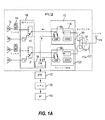
図1Aは、本開示の一態様による、ダイプレクサ200を使用する無線周波数(RF)フロントエンド(RFFE)モジュール100の概略図である。RFフロントエンドモジュール100は、電力増幅器102と、デュプレクサ/フィルタ104と、無線周波数(RF)スイッチモジュール106とを含む。電力増幅器102は、信号を送信のための特定の電力レベルに増幅する。デュプレクサ/フィルタ104は、周波数、挿入損失、拒絶、または他の同様のパラメータを含む様々な異なるパラメータに応じて入出力信号をフィルタ処理する。さらに、RFスイッチモジュール106は、RFフロントエンドモジュール100の残りの部分に渡す入力信号の特定の部分を選択してもよい。
FIG. 1A is a schematic diagram of a radio frequency (RF) front end (RFFE)
RFフロントエンドモジュール100はまた、チューナー回路112(たとえば、第1のチューナー回路112Aおよび第2のチューナー回路112B)と、ダイプレクサ200と、キャパシタ116と、インダクタ118と、接地端子115と、アンテナ114とを含む。チューナー回路112(たとえば、第1のチューナー回路112Aおよび第2のチューナー回路112B)は、チューナー、ポータブルデータ入力端末(PDET)、およびハウスキーピングアナログデジタル変換器(HKADC)などの構成要素を含む。チューナー回路112は、アンテナ114のインピーダンス同調(たとえば、電圧定在波比(VSWR)最適化)を実行してもよい。RFフロントエンドモジュール100は、ワイヤレストランシーバ(WTR)120に結合された受動コンバイナ108も含む。受動コンバイナ108は、第1のチューナー回路112Aおよび第2のチューナー回路112Bからの検出された電力を組み合わせる。ワイヤレストランシーバ120は、受動コンバイナ108からの情報を処理し、この情報をモデム130(たとえば、移動局モデム(MSM))に提供する。モデム130は、デジタル信号をアプリケーションプロセッサ(AP)140に与える。
The RF
図1Aに示すように、ダイプレクサ200は、チューナー回路112のチューナー構成要素とキャパシタ116、インダクタ118、およびアンテナ114との間に位置する。ダイプレクサ200は、アンテナ114とチューナー回路112との間に配置され、RFフロントエンドモジュール100から、ワイヤレストランシーバ120と、モデム130と、アプリケーションプロセッサ140とを含むチップセットへ高システム性能を提供することができる。ダイプレクサ200は、ハイバンド周波数とローバンド周波数の両方に対して周波数ドメイン多重化も実行する。ダイプレクサ200が入力信号に対してダイプレクサ200の周波数多重化機能を実行した後、ダイプレクサ200の出力が、キャパシタ116とインダクタ118とを含む任意のLC(インダクタ/キャパシタ)ネットワークに送られる。LCネットワークは、必要に応じて、アンテナ114の追加のインピーダンス整合構成要素を構成してもよい。その場合、特定の周波数を有する信号がアンテナ114によって送信または受信される。単一のキャパシタおよびインダクタが示されているが、複数の構成要素も企図される。
As shown in FIG. 1A,
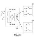
図1Bは、本開示の一態様による、キャリアアグリゲーションを実現するためのチップセット160用の、第1のダイプレクサ200-1を含むワイヤレスローカルエリアネットワーク(WLAN)(たとえば、WiFi)モジュール170および第2のダイプレクサ200-2を含むRFフロントエンドモジュール150の概略図である。WiFiモジュール170は、アンテナ192をワイヤレスローカルエリアネットワークモジュール(たとえば、WLANモジュール172)に通信可能に結合する第1のダイプレクサ200-1を含む。RFフロントエンドモジュール150は、アンテナ194をデュプレクサ180を介してワイヤレストランシーバ(WTR)120に通信可能に結合する第2のダイプレクサ200-2を含む。ワイヤレストランシーバ120およびWiFiモジュール170のWLANモジュール172は、電力管理集積回路(PMIC)156を介して電源152によって電力を供給されるモデム(MSM、たとえばベースバンドモデム)130に結合される。チップセット160は、信号完全性を実現するためにキャパシタ162および164ならびにインダクタ166も含む。PMIC156、モデム130、ワイヤレストランシーバ120、およびWLANモジュール172の各々は、キャパシタ(たとえば、158、132、122、および174)を含み、クロック154に従って動作する。チップセット160における様々なインダクタ構成要素およびキャパシタ構成要素の形状および配置によって、各構成要素間の電磁結合が低減し得る。
FIG.1B shows a wireless local area network (WLAN) (e.g., WiFi) module 170 and a second including a first diplexer 200-1 for a
図2Aは、本開示の一態様によるダイプレクサ200の図である。ダイプレクサ200は、ハイバンド(HB)入力ポート212と、ローバンド(LB)入力ポート214と、アンテナ216とを含む。ダイプレクサ200のハイバンドパスはハイバンドアンテナスイッチ210-1を含む。ダイプレクサ200のローバンドパスはローバンドアンテナスイッチ210-2を含む。RFフロントエンドモジュールを含むワイヤレスデバイスは、アンテナスイッチ210およびダイプレクサ200を使用してワイヤレスデバイスのRF入力およびRF出力用の広範囲のバンドを使用可能にし得る。さらに、アンテナ216は多入力多出力(MIMO)アンテナであってもよい。多入力多出力アンテナは、キャリアアグリゲーションなどの機能をサポートするためにワイヤレスデバイスのRFフロントエンドに広く使用される。
FIG. 2A is a diagram of a
図2Bは、本開示の一態様によるRFフロントエンドモジュール250の図である。RFフロントエンドモジュール250は、図2Aに示されている広範囲の帯域を使用可能にするためにアンテナスイッチ(ASW)210とダイプレクサ200(またはトリプレクサ)とを含む。さらに、RFフロントエンドモジュール250は、基板202によって支持されるフィルタ230と、RFスイッチ220と、電力増幅器218とを含む。フィルタ230は、RFフロントエンドモジュール250における高次高調波を防止するためにダイプレクサ、トリプレクサ、ローパスフィルタ、バランフィルタ、および/またはノッチフィルタを形成するように基板202に沿って配置されたインダクタ(L)とキャパシタ(C)とを有する様々なLCフィルタを含んでもよい。ダイプレクサ200は、システムボード201(たとえば、プリント回路板(PCB)またはパッケージ基板)上の表面実装型デバイス(SMD)として実装されてもよい。代替的に、ダイプレクサ200は、基板202上に実装されてもよい。
FIG. 2B is a diagram of an RF
この構成では、RFフロントエンドモジュール250は、シリコンオンインシュレータ(SOI)技術を使用して実装され、SOI技術は、RFフロントエンドモジュール250内の高次高調波の低減を助ける。SOI技術は、寄生デバイスキャパシタンスを低減して性能を改善するために、従来のシリコン基板を層状シリコンオンインシュレータ基板に置き換える。シリコン接合は電気的絶縁体、典型的には埋込み酸化物(BOX)層の上にあるので、SOIベースのデバイスは、従来のシリコン製デバイスとは異なる。しかしながら、低減された厚さのBOX層は、(シリコン層上の)能動デバイスとBOX層を支持する基板との間が近接することによって生じる寄生キャパシタンスを十分に低減しない場合がある。その結果、本開示の態様は、図3A〜図3Eに示すように、能動デバイスを基板からさらに分離するための層転写プロセスを含む。
In this configuration, the RF
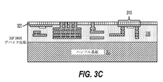
図3A〜図3Eは、本開示の態様による、層転写プロセスの間の集積無線周波数(RF)回路構造300の断面図を示す。図3Aに示すように、RFシリコンオンインシュレータ(SOI)デバイスは、犠牲基板301(たとえば、バルクウエハ)によって支持される埋込み酸化物(BOX)層320上に能動デバイス310を含む。RF SOIデバイスはまた、第1の誘電体層306内部で能動デバイス310に結合される相互接続350を含む。図3Bに示すように、ハンドル基板302が、第1の誘電体層306に接合される。
3A-3E illustrate cross-sectional views of an integrated radio frequency (RF)
図3Bに示すように、ハンドル基板302は、RF SOIデバイスの前面誘電体層306に接合される。加えて、犠牲基板301が除去される。層転写プロセスを使用して犠牲基板301を除去することで、誘電体の厚さが増加することによって、高性能で低寄生のRFデバイスが可能になる。すなわち、RF SOIデバイスの寄生キャパシタンスは、能動デバイス310とハンドル基板302との間の距離を決定する誘電体厚さに比例する。
As shown in FIG. 3B, the
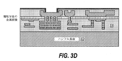
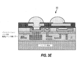
図3Cに示すように、RF SOIデバイスは、ハンドル基板302が固定されて犠牲基板301が除去された時点で反転される。図3Dに示すように、層転写後の金属被覆プロセスは、たとえば、通常の相補型金属酸化物半導体(CMOS)プロセスを使用して実行される。図3Eに示すように、集積RF回路構造300は、パッシベーション層を堆積させることと、ボンドパッドを開くことと、再配線層(redistribution layer)を堆積させることと、集積RF回路構造300をシステムボード(たとえば、プリント回路板(PCB))に接合することを可能にするために導電バンプ/ピラーを形成することとによって達成される。
As shown in FIG. 3C, the RF SOI device is inverted when the
再び図3Aを参照すると、RF SOIデバイスは、犠牲基板301とBOX層320との間にトラップリッチ層を含んでもよい。加えて、犠牲基板301はハンドル基板302と置き換えられてもよく、BOX層320の厚さは高調波を改善するために増加されてもよい。RF SOIデバイスのこの配置は、純シリコンまたはSOI実装に対して改善された高調波をもたらし得るが、RF SOIデバイスは、特にシリコンハンドル基板が使用されるときに、ハンドル基板からの非線型応答によって制限される。すなわち、図3Aでは、図3B〜図3Eに示す構成に対して、増加された厚さのBOX層320は、能動デバイス310と犠牲基板301との間に十分な距離をもたらさない。その上、RF SOIデバイスは、一般に、SOI層の一方の面上のCMOSトランジスタ形成に限定される。
Referring again to FIG. 3A, the RF SOI device may include a trap rich layer between the sacrificial substrate 301 and the
図4は、本開示の態様による、層転写プロセスを使用して製作された集積RF回路構造400の断面図である。代表的に、集積RF回路構造400は、絶縁層430上に形成されたゲート、ボディ、およびソース/ドレイン領域を有する能動デバイス410を含む。シリコンオンインシュレータ(SOI)実装形態では、絶縁層430は埋込み酸化物(BOX)層であり、ボディおよびソース/ドレイン領域は、BOX層によって支持されるシャロートレンチ分離(STI:shallow trench isolation)領域を含むSOI層から形成される。
FIG. 4 is a cross-sectional view of an integrated
集積RF回路構造400はまた、能動デバイス410のソース/ドレイン領域に結合された中間工程(MEOL)/配線工程(BEOL)相互接続を含む。説明するように、MEOL/BEOL層は、前面層と呼ばれる。対照的に、絶縁層430を支持する層は、裏面層と呼ばれることがある。この用語に従って、前面相互接続470は、前面誘電体層404内の前面接点412を介して能動デバイス410のソース/ドレイン領域に結合される。加えて、ハンドル基板402は、前面誘電体層404に結合される。この構成では、裏面誘電体440は絶縁層430に隣接し、場合によっては絶縁層430を支持する。加えて、裏面金属被覆450は、前面相互接続470に結合される。
The integrated
図4に示すように、層転写プロセスは、集積RF回路構造400の高調波を改善するために、能動デバイス410とハンドル基板402との間の分離を増加させる。層転写プロセスは、高性能、低寄生のRFのデバイスを可能にするが、集積RF回路構造400は、フローティングボディ効果の欠点がある。すなわち、SOI技術を使用して製作された能動デバイスは、一般に、トランジスタのボディが絶縁された基板に対してキャパシタを形成する、フローティングボディ効果の欠点がある。フローティングボディ効果は、特に、しきいの電圧制御およびボディ充電制御がフローティングボディ効果によって妨げられるアナログデバイスにおいて深刻である。ボディ接点は、フローティングボディ効果を防止するために使用され得る。残念ながら、ボディ接点の使用は、顕著なエリアペナルティをもたらす。その結果、本開示の態様は、ディープトレンチ能動デバイスに対する裏面ボディタイの形成を可能にするための層転写後のプロセスを含む。
As shown in FIG. 4, the layer transfer process increases the separation between the
本開示の様々な態様は、集積回路構造に対する裏面ボディタイの形成を可能にするための、層転写後のプロセスのための技法を提供する。対照的に、基板工程(FEOL)プロセスの間に形成された能動デバイスへのアクセスは、従来では、能動デバイスのゲートおよびソース/ドレイン領域と配線工程(BEOL)相互接続層(たとえば、M1、M2など)との間に接点を設ける中間工程(MEOL)処理の間に設けられる。本開示の態様は、クオリティ(Q)ファクタの高いRFアプリケーションに対する集積無線周波数(RF)回路構造内でアンテナスイッチトランジスタとして使用され得る裏面ボディタイを有するディープトレンチスイッチトランジスタを形成するための層転写後のプロセスを伴う。他のアプリケーションは、低電力増幅器モジュール、低ノイズ増幅器、およびアンテナダイバーシティスイッチ内の能動デバイスを含む。 Various aspects of the present disclosure provide techniques for post-layer transfer processes to enable the formation of backside body ties for integrated circuit structures. In contrast, access to active devices formed during the substrate process (FEOL) process has traditionally been the gate and source / drain regions of the active device and the wiring process (BEOL) interconnect layers (e.g., M1, M2 Etc.) are provided during an intermediate process (MEOL) process in which contacts are provided between them. Aspects of the present disclosure provide for post layer transfer to form a deep trench switch transistor having a backside body tie that can be used as an antenna switch transistor in an integrated radio frequency (RF) circuit structure for high quality (Q) factor RF applications. With the process. Other applications include low power amplifier modules, low noise amplifiers, and active devices in antenna diversity switches.
図5は、本開示の態様による、裏面ボディタイを有するディープトレンチ能動デバイス(たとえば、スイッチトランジスタ)を含む集積回路構造500の断面図である。本開示の態様では、層転写後のプロセスは、従来のシリコンオンインシュレータ製作プロセスに関連するフローティングボディ効果を解決する、裏面ボディタイの形成を可能にする。典型的に、集積回路構造500は、絶縁層530の前面上にあり、かつ絶縁層530の裏面まで通して延びる、ディープトレンチ能動デバイス510を含む。この構成では、ディープトレンチ能動デバイス510のボディは、半導体層(たとえば、SOI実装形態に対するシリコン)から形成された半導体ピラー512から構成される。ピラーは、より長い長さがより小さい面積内で取得される(たとえば、「アコーディオン」効果)限り、間隔が密である必要はない。加えて、ゲートは、半導体ピラー512とインターロックし、誘電体材料層522(たとえば、ゲート誘電体)によって分離され、絶縁層530を通って延びるゲートフィンガー520から構成される。
FIG. 5 is a cross-sectional view of an
絶縁層530は、シリコンオンインシュレータ(SOI)実装形態に対する埋込み酸化物(BOX)層とすることができ、ボディおよびソース/ドレイン領域(図示せず)は、SOI層から形成される。代替的に、絶縁層530は、第1のトレンチタイプ能動デバイス580および第2のトレンチタイプ能動デバイス590からディープトレンチ能動デバイス510を分離するためのディープトレンチ絶縁領域とすることができる。第1のトレンチタイプ能動デバイス580および第2のトレンチタイプ能動デバイス590に関する追加の詳細は、本開示の詳細を不明瞭にすることを回避するために省略される。加えて、トレンチタイプスイッチトランジスタは、ディープトレンチスイッチトランジスタのドレイン領域およびソース領域を設けるために、n型(たとえば、第1のドープ領域)およびp型(たとえば、第2のドープ領域)半導体領域をドープするための注入プロセスに応じて、negative金属酸化物半導体(NMOS)スイッチトランジスタまたはpositive MOS(PMOSトランジスタ)として構成され得る。
The insulating
本開示のこの態様では、集積回路構造500はまた、絶縁層530の前面と対向する裏面を支持する裏面誘電体層540内に配置された裏面金属被覆550を含む。本開示の態様による裏面金属被覆550は、ディープトレンチ能動デバイス510に対する低抵抗ボディタイを提供する。この構成では、裏面金属被覆550の第1の部分550-1は、接点プラグ552および裏面シリサイド層554を介してディープトレンチ能動デバイス510のボディに電気的に結合される。ディープトレンチ能動デバイス510のこの構成は、裏面金属被覆550をボディに電気的に結合することによってフローティングボディ効果を防止する。
In this aspect of the present disclosure, the
集積回路構造500はまた、前面誘電体層504内に配置された前面金属被覆570(たとえば、第1のBEOL相互接続(M1))を含む。前面金属被覆570は、ビア560を通して裏面金属被覆550の第2の部分550-2に結合される。裏面誘電体層540内の裏面金属被覆550の第2の部分550-2は、接点プラグ552および裏面シリサイド層554のうちの1つを介して第2のトレンチタイプ能動デバイス590のボディに電気的に結合される。加えて、ハンドル基板502は、前面誘電体層504に結合される。裏面誘電体層540は、絶縁層530に隣接し、場合によっては絶縁層530を支持する。この構成では、層転写後の金属被覆プロセスは、裏面金属被覆550を形成する。図5に示すように、前面金属被覆570は、裏面金属被覆550から遠位に配置される。
本開示の態様によれば、ハンドル基板502は、シリコンなどの半導体材料から構成され得る。この構成では、ハンドル基板502は、少なくとも1つの他の能動デバイスを含み得る。代替的に、ハンドル基板502は、寄生キャパシタンスを低減することによって高調波をさらに改善するために受動基板であり得る。この構成では、ハンドル基板502は、少なくとも1つの他の受動デバイスを含み得る。本明細書における説明では、「受動基板」という用語は、ダイシングされたウエハまたはパネルの基板を指す場合があるか、または、ダイシングされていないウエハ/パネルの基板を指す場合がある。一構成では、受動基板は、ガラス、空気、石英、サファイア、高抵抗シリコン、または他の同様の受動材料で構成される。受動基板はまた、コアレス基板であってもよい。 According to aspects of the present disclosure, the handle substrate 502 can be composed of a semiconductor material such as silicon. In this configuration, the handle substrate 502 may include at least one other active device. Alternatively, the handle substrate 502 can be a passive substrate to further improve harmonics by reducing parasitic capacitance. In this configuration, the handle substrate 502 may include at least one other passive device. In the description herein, the term “passive substrate” may refer to a diced wafer or panel substrate, or may refer to an undiced wafer / panel substrate. In one configuration, the passive substrate is composed of glass, air, quartz, sapphire, high resistance silicon, or other similar passive material. The passive substrate may also be a coreless substrate.
「層」という用語は、膜を含み、別段述べられていない限り、垂直厚または水平厚を示すものと解釈されるべきではないことが理解されよう。本明細書において説明するように、「基板」という用語は、ダイシングされたウエハの基板を指す場合があるか、または、ダイシングされていないウエハの基板を指す場合がある。同様に、チップおよびダイという用語は、入れ換えられると信じることが難しくない限り、互換的に使用することができる。 It will be understood that the term “layer” includes a membrane and should not be construed as indicating vertical or horizontal thickness unless otherwise stated. As described herein, the term “substrate” may refer to a substrate of a diced wafer, or may refer to a substrate of an undiced wafer. Similarly, the terms chip and die can be used interchangeably unless it is difficult to believe that they will be interchanged.
本開示の態様では、図5〜図8に示すように、層転写後のプロセスは、トレンチタイプ能動デバイスのボディをつなぐために裏面金属被覆を形成する。裏面シリサイド化プロセスにおける変形形態が、図7〜図8に示される。加えて、半導体層(たとえば、シリコンオンインシュレータ層)に対する変形形態が、図7および図8に示される。本開示のさらなる態様によれば、ディープトレンチ能動デバイス510は、金属酸化物半導体(MOS)キャパシタとして構成され得る。この構成では、MOSキャパシタは、第1のプレートとしてゲートフィンガー520と、第2のプレートとして半導体ピラー512と、キャパシタ誘電体として誘電体材料層522とを含む。
In aspects of the present disclosure, as shown in FIGS. 5-8, the post-layer transfer process forms a backside metallization to connect the bodies of the trench type active devices. Variations in the backside silicidation process are shown in FIGS. In addition, variations on the semiconductor layer (eg, silicon on insulator layer) are shown in FIGS. According to a further aspect of the present disclosure, the deep trench
図6は、本開示の態様による、裏面ボディタイを有するトレンチタイプ能動デバイスを含む集積回路構造600の断面図である。認識されるように、集積回路構造600の構成は、図5の集積回路構造500の構成と同様である。しかしながら、図6に示す構成では、配線工程ビアプロセス(V0)が、ディープトレンチ能動デバイス510のボディの露出部分に対するシリサイドホールを形成するために使用される。すなわち、この構成では、裏面シリサイド層554(図5)は、図5に示すシリサイドの連続層ではなく、ディープトレンチ能動デバイス510のボディの露出部分上の離散要素として堆積される。加えて、裏面シリサイド層554(図5)は、第2のトレンチタイプ能動デバイス590のボディの露出部分上の離散要素として堆積される。
FIG. 6 is a cross-sectional view of an
それゆえ、本開示のこの態様はまた、トレンチタイプ能動デバイスのボディをつなぐための簡略化された層転写後のプロセスの裏面シリサイド化プロセスを行うことによって、従来のシリコンオンインシュレータ製作プロセスに関連するフローティングボディ効果問題を解決する。図6に示す構成は、たとえば、図7に示すように、SOIウエハではなくバルクウエハを使用して製作されることを認識されたい。 Therefore, this aspect of the present disclosure also relates to a conventional silicon-on-insulator fabrication process by performing a backside silicidation process of a simplified post-layer transfer process to connect the bodies of trench type active devices. Solve the floating body effect problem. It should be appreciated that the configuration shown in FIG. 6 is fabricated using a bulk wafer rather than an SOI wafer, for example, as shown in FIG.
図7は、本開示の態様による、裏面ボディタイを有するトレンチタイプ能動デバイスを含む集積回路構造700の断面図である。認識されるように、集積回路構造700の構成は、図6の集積回路構造600の構成と同様である。しかしながら、図7に示す構成では、増加した厚さの半導体層が、SOIウエハによって支持されるシリコンオンインシュレータ(SOI)層として設けられる。この構成では、絶縁層530は、ディープトレンチ能動デバイス510と、第1のトレンチタイプ能動デバイス580および第2のトレンチタイプ能動デバイス590との間のディープトレンチ絶縁層とすることができる。
FIG. 7 is a cross-sectional view of an
この構成によれば、ディープトレンチ能動デバイス510のボディはまた、絶縁層530によって支持される。接点プラグ552は、絶縁層530の一部分を通って延びる。加えて、裏面金属被覆550の第1の部分550-1および第2の部分550-2が、ディープトレンチ能動デバイス510および第2のトレンチタイプ能動デバイス590をつなぐために、絶縁層530の一部分および裏面誘電体層540の一部分の中に形成される。それゆえ、本開示のこの態様は、従来のシリコンオンインシュレータ製作プロセスに関連するフローティングボディ効果問題を解決する。
According to this configuration, the body of the deep trench
図8は、本開示の態様による、裏面ボディタイを有するトレンチタイプ能動デバイスを含む集積回路構造800の断面図である。認識されるように、集積回路構造800の構成は、図6の集積回路構造600の構成と同様である。しかしながら、図8に示す構成では、低減された厚さの半導体層が、SOIウエハによって支持されるシリコンオンインシュレータ(SOI)層として設けられる。この構成では、絶縁層530は、ディープトレンチ能動デバイス510と、第1のトレンチタイプ能動デバイス580および第2のトレンチタイプ能動デバイス590との間のディープトレンチ絶縁層532と組み合わされる。本開示の一態様では、ゲート入れ替えプロセスは、改善されたゲート形成に対するポリエッチ(poly etch)制限(たとえば、ライン/エッジ粗さ)を克服するために、ディープトレンチ能動デバイス510ならびに/または第1のトレンチタイプ能動デバイス580および第2のトレンチタイプ能動デバイス590を製作するために実行され得る。
FIG. 8 is a cross-sectional view of an
この構成によれば、ディープトレンチ能動デバイス510のボディの半導体ピラー512は、ディープトレンチ絶縁層532の一部分を通って延びる。加えて、半導体層の低減された厚さのために、ゲートは、半導体ピラー512とインターロックするゲートフィンガー520に結合された第1の部分524(たとえば、トレンチ)を含む。本開示のこの態様では、ディープトレンチ能動デバイス510は、裏面金属被覆550の第2の部分550-2によってバイアスされるトレンチ半導体層582を含む。本開示のこの態様は、裏面のバイアスされたトレンチタイプ能動デバイスとSOI実装形態とを組み合わせることによって従来のシリコンオンインシュレータ製作プロセスに関連するフローティングボディ効果問題を解決する。図8のディープトレンチトランジスタは、高電力または高電流トランジスタが望まれるときに有用である。
According to this configuration, the
図9は、本開示の一態様による、ディープトレンチ能動デバイスを含む集積回路構造を構築する方法900を示すプロセスフロー図である。ブロック902において、絶縁層内部の半導体層は、複数の半導体ピラーを含むボディを形成するためにエッチングされる。たとえば、図5に示すように、絶縁層530内部の半導体領域は、ディープトレンチ能動デバイス510のボディを形成するためにエッチングされる。ディープトレンチ能動デバイス510のボディは、絶縁層530の裏面から前面まで延びる半導体ピラー512を含む。シリコンオンインシュレータ(SOI)実装形態では、絶縁層530は埋込み酸化物(BOX)層であり、半導体層はシリコンオンインシュレータ(SOI)層である。しかしながら、本開示はシリコンオンインシュレータ実装形態に限定されない。
FIG. 9 is a process flow diagram illustrating a
再び図9を参照すると、ブロック904において、誘電体材料層が、絶縁層の前面上および半導体ピラーを分離するトレンチ内に堆積される。たとえば、図5に示すように、誘電体材料層522は、絶縁層530の前面上およびボディの半導体ピラー512上に堆積される。ブロック906において、半導体材料は、ゲートフィンガーを含むゲートを形成するために、誘電体材料層上および半導体ピラーを分離するトレンチ内に堆積される。たとえば、図5に示すように、半導体材料(たとえば、ポリシリコン材料)は、ディープトレンチ能動デバイス510のゲートを形成するために、誘電体材料層522およびボディの半導体ピラー512の上に堆積される。この構成では、ディープトレンチ能動デバイス510のゲートは、ボディの半導体ピラー512とインターロックするゲートフィンガー520から構成される。ディープトレンチの深さは、1〜5ミクロンの範囲内にあり得る。
Referring again to FIG. 9, at
従来のシリコンオンインシュレータ実装形態とは対照的に、ディープトレンチ能動デバイス510のボディは、図9にさらに示すように、ディープトレンチ能動デバイス510のボディをつなぐことによってフローティングを防止される。ブロック908において、ハンドル基板が、絶縁層の前面上の前面誘電体層に接合される。たとえば、図5に示すように、層転写プロセスが実行され、ハンドル基板502が前面誘電体層504に接合される。本開示のこの態様では、ディープトレンチ能動デバイス510のボディをつなぐことは、層転写後のプロセスの一部として実行される。
In contrast to conventional silicon-on-insulator implementations, the body of the deep trench
再び図9を参照すると、ブロック910において、裏面金属被覆が、絶縁層の裏面の表面を支持する裏面誘電体層内に製作される。裏面金属被覆は、少なくとも1つの裏面接点を介してディープトレンチ能動デバイスのボディに結合される。たとえば、図5に示すように、裏面金属被覆550は、ディープトレンチ能動デバイス510のボディに結合される。この構成では、裏面金属被覆550は、裏面シリサイド層554を介してディープトレンチ能動デバイス510のボディに結合された接点プラグ552に直接結合される。この構成では、ディープトレンチ能動デバイス510のボディは、層転写後のプロセスの一部として製作された裏面金属被覆550によってフローティングを防止される。
Referring again to FIG. 9, at block 910, a backside metal coating is fabricated in the backside dielectric layer that supports the backside surface of the insulating layer. The backside metallization is coupled to the body of the deep trench active device via at least one backside contact. For example, as shown in FIG. 5, backside metallization 550 is coupled to the body of deep trench
本開示のさらなる態様によれば、トレンチタイプ能動デバイスを含む集積回路が説明される。集積RF回路構造は、ゲートフィンガーを有するゲートと、ゲートのゲートフィンガーとインターロックする半導体ピラーを有するボディとを含む。集積RF回路はまた、ボディに結合された裏面接点を含み得る。集積回路は、裏面接点を介してボディをつなぐための手段をさらに含み得る。つなぐ手段は、図5〜図8に示す裏面金属被覆550とすることができる。別の態様では、前述の手段は、前述の手段によって列挙された機能を実行するように構成される任意のモジュールまたは任意の装置であってもよい。 According to a further aspect of the present disclosure, an integrated circuit including a trench type active device is described. The integrated RF circuit structure includes a gate having a gate finger and a body having a semiconductor pillar that interlocks with the gate finger of the gate. The integrated RF circuit may also include a back contact coupled to the body. The integrated circuit may further include means for connecting the body via the back contact. The connecting means can be the back surface metal coating 550 shown in FIGS. In another aspect, the aforementioned means may be any module or any device configured to perform the functions listed by the aforementioned means.
従来のシリコンオンインシュレータ製作プロセスは、フローティングボディ効果の欠点がある。本開示の態様は、クオリティ(Q)ファクタの高いRFアプリケーションに対する集積無線周波数(RF)回路構造内でアンテナスイッチトランジスタとして使用され得る裏面ボディ接点を有するディープトレンチスイッチトランジスタを説明する。一構成では、層転写前のプロセスは、ディープトレンチスイッチトランジスタを形成する。加えて、層転写後のプロセスは、ディープトレンチスイッチトランジスタのボディをつなぐための裏面ボディ接点を形成する。裏面ボディタイを形成する層転写後のプロセスは、ディープスイッチトランジスタのボディをフローティングから防止することによってフローティングボディ効果問題を解決する。裏面ボディ接点は、従来のボディ接点に関連するエリアペナルティまたは不要な抵抗経路を回避する。加えて、ゲートフィンガーを使用するディープトレンチスイッチトランジスタの配置は、ディープトレンチスイッチトランジスタのゲートによって占有される表面積を低減する。 Conventional silicon-on-insulator fabrication processes suffer from the floating body effect. Aspects of the present disclosure describe a deep trench switch transistor having a back body contact that can be used as an antenna switch transistor within an integrated radio frequency (RF) circuit structure for high quality (Q) factor RF applications. In one configuration, the pre-layer transfer process forms a deep trench switch transistor. In addition, the post-layer transfer process forms a back body contact to connect the body of the deep trench switch transistor. The post-layer transfer process that forms the back body tie solves the floating body effect problem by preventing the body of the deep switch transistor from floating. The back body contact avoids area penalties or unnecessary resistance paths associated with conventional body contacts. In addition, the placement of deep trench switch transistors using gate fingers reduces the surface area occupied by the gates of deep trench switch transistors.
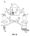
図10は、本開示の一態様が有利に利用される場合がある、例示的なワイヤレス通信システム1000を示すブロック図である。説明のために、図10は、3つのリモートユニット1020、1030、および1050、ならびに2つの基地局1040を示す。ワイヤレス通信システムがこれよりも多くのリモートユニットおよび基地局を有してもよいことが認識されよう。リモートユニット1020、1030および1050は、開示されたディープトレンチ能動デバイスを含むICデバイス1025A、1025C、および1025Bを含む。他のデバイスがまた、基地局、スイッチングデバイス、およびネットワーク機器などの、開示されたディープトレンチ能動デバイスを含んでもよいことが認識されよう。図10は、基地局1040からリモートユニット1020、1030、および1050への順方向リンク信号1080、ならびに、リモートユニット1020、1030、および1050から基地局1040への逆方向リンク信号1090を示す。
FIG. 10 is a block diagram illustrating an example
図10では、リモートユニット1020はモバイル電話として示され、リモートユニット1030はポータブルコンピュータとして示され、リモートユニット1050はワイヤレスローカルループシステム内の固定ロケーションリモートユニットとして示される。たとえば、リモートユニットは、モバイル電話、ハンドヘルドパーソナル通信システム(PCS)ユニット、携帯情報端末(PDA)などのポータブルデータユニット、GPS対応デバイス、ナビゲーションデバイス、セットトップボックス、音楽プレーヤ、ビデオプレーヤ、エンターテインメントユニット、メーター読取り機器などの固定ロケーションデータユニット、またはデータもしくはコンピュータ命令を記憶するかもしくは取り出す他の通信デバイス、あるいはそれらの組合せであってもよい。図10は本開示の態様によるリモートユニットを示すが、本開示はこれらの例示的に示されるユニットに限定されない。本開示の態様は、開示されたディープトレンチ能動デバイスを含む、多くのデバイスにおいて適切に採用され得る。
In FIG. 10,
図11は、上で開示されたディープトレンチ能動デバイスのような、半導体構成要素の回路設計、レイアウト設計、および論理設計のために使用される、設計用ワークステーションを示すブロック図である。設計用ワークステーション1100は、オペレーティングシステムソフトウェアと、サポートファイルと、CadenceまたはOrCADなどの設計ソフトウェアが入っているハードディスク1101を含む。設計用ワークステーション1100はまた、回路1110、またはディープトレンチ能動デバイスなどの半導体構成要素1112の設計を容易にするためにディスプレイ1102を含む。回路設計1110または半導体構成要素1112を有形に記憶するために記憶媒体1104が設けられる。回路設計1110または半導体構成要素1112は、GDSIIやGERBERなどのファイルフォーマットで記憶媒体1104上に格納されてもよい。記憶媒体1104は、CD-ROM、DVD、ハードディスク、フラッシュメモリ、または他の適切なデバイスであってもよい。さらに、設計用ワークステーション1100は、記憶媒体1104から入力を受け取るか、または記憶媒体1104に出力を書き込むためのドライブ装置1103を含む。
FIG. 11 is a block diagram illustrating a design workstation used for circuit design, layout design, and logic design of semiconductor components, such as the deep trench active devices disclosed above. The
記憶媒体1104上に記録されたデータは、論理回路構成、フォトリソグラフィマスクのためのパターンデータ、または電子ビームリソグラフィなどのシリアル書込みツールのためのマスクパターンデータを指定してもよい。データはさらに、論理シミュレーションに関連したタイミング図やネット回路などの論理検証データを含んでもよい。記憶媒体1104上にデータを用意すると、半導体ウエハを設計するためのプロセスの数が減少することによって、回路設計1110または半導体構成要素1112の設計が容易になる。
Data recorded on
ファームウェアおよび/またはソフトウェアの実装形態の場合、この方法は、本明細書で説明した機能を実行するモジュール(たとえば、プロシージャ、関数など)を用いて実装されてもよい。本明細書で説明する方法を実施する際に、命令を有形に具現する機械可読媒体が使用されてもよい。たとえば、ソフトウェアコードは、メモリに記憶され、プロセッサユニットによって実行されてもよい。メモリは、プロセッサユニット内に実装されてもよくあるいはプロセッサユニットの外部に実装されてもよい。本明細書において使用される「メモリ」という用語は、長期メモリ、短期メモリ、揮発性メモリ、不揮発性メモリ、または他のメモリのタイプを指し、特定のタイプのメモリもしくは特定の数のメモリ、またはメモリが格納される媒体のタイプに限定すべきではない。 For firmware and / or software implementations, the method may be implemented using modules (eg, procedures, functions, etc.) that perform the functions described herein. In performing the methods described herein, machine readable media that tangibly embodies instructions may be used. For example, the software code may be stored in memory and executed by a processor unit. The memory may be implemented in the processor unit or may be implemented outside the processor unit. The term “memory” as used herein refers to a type of long-term memory, short-term memory, volatile memory, non-volatile memory, or other memory, a specific type of memory or a specific number of memories, or It should not be limited to the type of media on which the memory is stored.
各機能は、ファームウェアおよび/またはソフトウェアにおいて実装される場合、コンピュータ可読媒体上の1つまたは複数の命令またはコードとして記憶されてもよい。例には、データ構造を用いて符号化されたコンピュータ可読媒体、およびコンピュータプログラムを用いて符号化されたコンピュータ可読媒体が含まれる。コンピュータ可読媒体は、物理的なコンピュータ記憶媒体を含む。記憶媒体は、コンピュータによってアクセスできる入手可能な媒体であってもよい。限定ではなく例として、そのようなコンピュータ可読媒体は、RAM、ROM、EEPROM、CD-ROMもしくは他の光ディスクストレージ、磁気ディスクストレージもしくは他の磁気記憶デバイス、または、所望のプログラムコードを命令もしくはデータ構造の形で記憶するために使用することができるとともに、コンピュータによってアクセスすることができる他の媒体を含むことができ、本明細書において使用されるディスク(disk)およびディスク(disc)は、コンパクトディスク(disc)(CD)、レーザーディスク(登録商標)(disc)、光ディスク(disc)、デジタル多用途ディスク(disc)(DVD)、フロッピーディスク(disk)、およびブルーレイディスク(disc)を含み、ディスク(disk)は通常、データを磁気的に再生し、ディスク(disc)はデータをレーザーを用いて光学的に再生する。上記の組合せもコンピュータ可読媒体の範囲に含まれるべきである。 Each function may be stored as one or more instructions or code on a computer-readable medium when implemented in firmware and / or software. Examples include computer readable media encoded using a data structure and computer readable media encoded using a computer program. Computer-readable media includes physical computer storage media. A storage media may be any available media that can be accessed by a computer. By way of example, and not limitation, such computer-readable media may include RAM, ROM, EEPROM, CD-ROM or other optical disk storage, magnetic disk storage or other magnetic storage device, or instructions or data structures with desired program code. Can be used to store in the form of and can include other media that can be accessed by a computer, and the disks and discs used herein are compact disks (disc) (CD), laser disc (registered trademark) (disc), optical disc (disc), digital versatile disc (DVD), floppy disc (disk), and Blu-ray disc (disc) The disk normally reproduces data magnetically, and the disc optically reproduces data using a laser. Combinations of the above should also be included within the scope of computer-readable media.
コンピュータ可読媒体上のストレージに加えて、命令および/またはデータは、通信装置に含まれる伝送媒体上の信号として備えられてもよい。たとえば、通信装置は、命令およびデータを示す信号を有するトランシーバを含んでもよい。命令およびデータは、1つまたは複数のプロセッサに、請求項に概説される機能を実施させるように構成される。 In addition to storage on a computer-readable medium, instructions and / or data may be provided as a signal on a transmission medium included in the communication device. For example, the communication device may include a transceiver having signals indicative of instructions and data. The instructions and data are configured to cause one or more processors to perform the functions outlined in the claims.
本開示およびその利点について詳細に説明したが、添付の特許請求の範囲によって定義される本開示の技術から逸脱することなく、明細書において様々な変更、置換、および改変を施すことができることを理解されたい。たとえば、「上」および「下」などの関係語が、基板または電子デバイスに関して使用される。当然、基板または電子デバイスが反転される場合、上は下に、下は上になる。加えて、横向きの場合、上および下は、基板または電子デバイスの側面を指すことがある。さらに、本出願の範囲は、本明細書で説明したプロセス、機械、製造、ならびに組成物、手段、方法、およびステップの特定の構成に限定されることを意図していない。本開示から当業者が容易に諒解するように、本明細書で説明する対応する構成と実質的に同じ機能を実行するかまたは実質的にそれと同じ結果を達成する、現存するかまたは今後開発されるプロセス、機械、製造、組成物、手段、方法、またはステップが、本開示に従って利用されてもよい。したがって、添付の特許請求の範囲は、そのようなプロセス、機械、製造、組成物、手段、方法、またはステップをそれらの範囲内に含むことを意図する。 Although the present disclosure and its advantages have been described in detail, it will be understood that various changes, substitutions and modifications can be made in the specification without departing from the technology of the present disclosure as defined by the appended claims. I want to be. For example, related terms such as “above” and “below” are used with respect to a substrate or electronic device. Of course, when the substrate or electronic device is inverted, the top is down and the bottom is up. In addition, when in landscape orientation, top and bottom may refer to the sides of the substrate or electronic device. Furthermore, the scope of the present application is not intended to be limited to the particular configurations of the processes, machines, manufacture, and compositions, means, methods, and steps described herein. As will be readily appreciated by those skilled in the art from this disclosure, existing or later developed that perform substantially the same function or achieve substantially the same results as the corresponding configurations described herein. Any process, machine, manufacture, composition, means, method, or step may be utilized in accordance with the present disclosure. Accordingly, the appended claims are intended to include within their scope such processes, machines, manufacture, compositions of matter, means, methods, or steps.
100 無線周波数(RF)フロントエンド(RFFE)モジュール
102 電力増幅器
104 デュプレクサ/フィルタ
106 RFスイッチモジュール
108 受動コンバイナ
112 チューナー回路
112A 第1のチューナー回路
112B 第2のチューナー回路
114 アンテナ
115 接地端子
116 キャパシタ
118 インダクタ
120 ワイヤレストランシーバ(WTR)
122 キャパシタ
130 モデム
132 キャパシタ
140 アプリケーションプロセッサ
150 RFフロントエンドモジュール
152 電源
154 クロック
156 電力管理集積回路(PMIC)
158 キャパシタ
160 チップセット
162 キャパシタ
164 キャパシタ
166 インダクタ
170 WiFiモジュール
172 WLANモジュール
174 キャパシタ
180 デュプレクサ
192 アンテナ
194 アンテナ
200 ダイプレクサ
200-1 第1のダイプレクサ
200-2 第2のダイプレクサ
201 システムボード
202 基板
210 アンテナスイッチ(ASW)
210-1 ハイバンドアンテナスイッチ
210-2 ローバンドアンテナスイッチ
212 ハイバンド(HB)入力ポート
214 ローバンド(LB)入力ポート
216 アンテナ
218 電力増幅器
220 RFスイッチ
230 フィルタ
250 RFフロントエンドモジュール
300 RF回路構造
301 犠牲基板
302 ハンドル基板
306 第1の誘電体層
310 能動デバイス
320 埋込み酸化物(BOX)層
350 相互接続
400 集積RF回路構造
402 ハンドル基板
404 前面誘電体層
410 能動デバイス
412 前面接点
430 絶縁層
440 裏面誘電体
450 裏面金属被覆
470 前面相互接続
500 集積回路構造
502 ハンドル基板
504 前面誘電体層
510 ディープトレンチ能動デバイス
512 半導体ピラー
520 ゲートフィンガー
522 誘電体材料層
524 第1の部分
530 絶縁層
532 ディープトレンチ絶縁層
540 裏面誘電体層
550 裏面金属被覆
550-1 第1の部分
550-2 第2の部分
552 接点プラグ
554 裏面シリサイド層
560 ビア
570 前面金属被覆
580 第1のトレンチタイプ能動デバイス
582 トレンチ半導体層
590 第2のトレンチタイプ能動デバイス
600 集積回路構造
700 集積回路構造
800 集積回路構造
900 方法
1000 ワイヤレス通信システム
1020 リモートユニット
1025A ICデバイス
1025B ICデバイス
1025C ICデバイス
1030 リモートユニット
1040 基地局
1050 リモートユニット
1080 順方向リンク信号
1090 逆方向リンク信号
1100 設計用ワークステーション
1101 ハードディスク
1102 ディスプレイ
1103 ドライブ装置
1104 記憶媒体
1110 回路設計
1112 半導体構成要素
100 Radio Frequency (RF) Front End (RFFE) module
102 Power amplifier
104 duplexer / filter
106 RF switch module
108 Passive combiner
112 Tuner circuit
112A first tuner circuit
112B Second tuner circuit
114 Antenna
115 Ground terminal
116 capacitors
118 inductor
120 wireless transceiver (WTR)
122 capacitors
130 modem
132 capacitors
140 Application processor
150 RF front-end module
152 Power supply
154 clock
156 Power Management Integrated Circuit (PMIC)
158 capacitor
160 chipsets
162 capacitors
164 capacitors
166 Inductor
170 WiFi module
172 WLAN module
174 capacitors
180 duplexers
192 antenna
194 Antenna
200 Diplexer
200-1 First diplexer
200-2 Second diplexer
201 System board
202 substrate
210 Antenna switch (ASW)
210-1 High band antenna switch
210-2 Low-band antenna switch
212 High-band (HB) input port
214 Low-band (LB) input port
216 antenna
218 Power amplifier
220 RF switch
230 Filter
250 RF front-end module
300 RF circuit structure
301 Sacrificial substrate
302 Handle board
306 First dielectric layer
310 active devices
320 Embedded oxide (BOX) layer
350 interconnect
400 Integrated RF circuit structure
402 Handle board
404 Front dielectric layer
410 active devices
412 Front contact
430 Insulation layer
440 Backside dielectric
450 Back side metal coating
470 Front interconnection
500 Integrated circuit structure
502 Handle board
504 Front dielectric layer
510 deep trench active devices
512 semiconductor pillar
520 Gate finger
522 Dielectric material layer
524 1st part
530 Insulation layer
532 Deep trench insulation layer
540 Back dielectric layer
550 Back metallization
550-1 first part
550-2 second part
552 contact plug
554 Backside silicide layer
560 beer
570 front metallization
580 First trench type active device
582 Trench semiconductor layer
590 Second trench type active device
600 Integrated circuit structure
700 Integrated circuit structure
800 integrated circuit structure
900 methods
1000 wireless communication system
1020 Remote unit
1025A IC device
1025B IC device
1025C IC device
1030 Remote unit
1040 base station
1050 remote unit
1080 Forward link signal
1090 Reverse link signal
1100 Design workstation
1101 hard disk
1102 display
1103 Drive device
1104 Storage media
1110 Circuit design
1112 Semiconductor components
Claims (25)
前記複数のゲートフィンガーとインターロックする複数の半導体ピラーを含むボディと、
前記ボディに結合された少なくとも1つの裏面接点と、
前記少なくとも1つの裏面接点を介して前記ボディに結合された裏面金属被覆とを備える、集積回路。 A gate including a plurality of gate fingers;
A body including a plurality of semiconductor pillars interlocking with the plurality of gate fingers;
At least one back contact coupled to the body;
An integrated circuit comprising a backside metallization coupled to the body via the at least one backside contact.
前記ゲートの前記第1の側に対向する第2の側に近接した前記ボディの第2のドープ領域とをさらに備える、請求項1に記載の集積回路。 A first doped region of the body proximate to the first side of the gate;
2. The integrated circuit of claim 1, further comprising a second doped region of the body proximate to a second side opposite the first side of the gate.
前記埋込み酸化物層を支持する裏面誘電体層とをさらに備え、前記ボディが前記埋込み酸化物層を通って延びて前記裏面誘電体層によって支持され、前記裏面接点および前記裏面金属被覆が前記裏面誘電体層内にある、請求項1に記載の集積回路。 A buried oxide (BOX) layer;
A back dielectric layer supporting the buried oxide layer, the body extending through the buried oxide layer and supported by the back dielectric layer, wherein the back contact and the back metal coating are the back surface The integrated circuit of claim 1, wherein the integrated circuit is in the dielectric layer.
前記埋込み酸化物層を支持する裏面誘電体層とをさらに備え、前記ボディが前記埋込み酸化物層内に延び、前記裏面接点が前記埋込み酸化物層内に延びて、前記ボディおよび前記裏面金属被覆に結合する、請求項1に記載の集積回路。 A buried oxide (BOX) layer;
A back dielectric layer supporting the buried oxide layer, the body extending into the buried oxide layer, the back contact extending into the buried oxide layer, and the body and the back metallization. The integrated circuit of claim 1, wherein the integrated circuit is coupled to.
前記埋込み酸化物層を支持する裏面誘電体層とをさらに備える、請求項1に記載の集積回路。 A buried oxide layer in which a first portion of the gate extends through a buried oxide layer, wherein the first portion is coupled to the plurality of gate fingers;
The integrated circuit of claim 1, further comprising a backside dielectric layer that supports the buried oxide layer.
複数の半導体ピラーを含むボディを形成するために絶縁層内部の半導体層をエッチングするステップと、
前記絶縁層の前面上および前記複数の半導体ピラーの表面上に誘電体材料層を堆積させるステップと、
複数のゲートフィンガーを含むゲートを形成するために、前記誘電体材料層上および前記複数の半導体ピラーを分離する複数のトレンチ内に半導体材料を堆積させるステップであって、前記複数のゲートフィンガーが前記複数の半導体ピラーとインターロックする、ステップと、
前記絶縁層の前記前面上の前面誘電体層にハンドル基板を接合するステップと、
前記絶縁層の裏面を支持する裏面誘電体層内に裏面金属被覆を製作するステップとを含み、前記裏面金属被覆が少なくとも1つの裏面接点を介して前記ボディに結合される、方法。 A method for constructing an integrated circuit comprising:
Etching a semiconductor layer inside the insulating layer to form a body including a plurality of semiconductor pillars;
Depositing a dielectric material layer on a front surface of the insulating layer and on a surface of the plurality of semiconductor pillars;
Depositing a semiconductor material on the dielectric material layer and in a plurality of trenches separating the plurality of semiconductor pillars to form a gate including a plurality of gate fingers, wherein the plurality of gate fingers are Interlocking with a plurality of semiconductor pillars, and
Bonding a handle substrate to a front dielectric layer on the front surface of the insulating layer;
Fabricating a backside metallization in a backside dielectric layer that supports the backside of the insulating layer, wherein the backside metallization is coupled to the body via at least one backside contact.
前記ゲートの前記第1の側に対向する第2の側に近接した前記ボディの第2のドープ領域をドープするステップとをさらに含む、請求項14に記載の方法。 Doping a first doped region of the body proximate to the first side of the gate;
15. The method of claim 14, further comprising: doping a second doped region of the body proximate a second side opposite the first side of the gate.
前記複数のゲートフィンガーとインターロックする複数の半導体ピラーを含むボディと、
前記ボディに結合された少なくとも1つの裏面接点と、
前記少なくとも1つの裏面接点を介して前記ボディをつなぐための手段とを備える、集積回路。 A gate including a plurality of gate fingers;
A body including a plurality of semiconductor pillars interlocking with the plurality of gate fingers;
At least one back contact coupled to the body;
Means for connecting the body via the at least one back contact.
前記ゲートの前記第1の側に対向する第2の側に近接した前記ボディの第2のドープ領域とをさらに備える、請求項21に記載の集積回路。 A first doped region of the body proximate to the first side of the gate;
24. The integrated circuit of claim 21, further comprising a second doped region of the body proximate to a second side opposite the first side of the gate.
前記スイッチトランジスタの出力に結合されたアンテナとを備える、無線周波数(RF)フロントエンドモジュール。 An integrated RF circuit comprising a deep trench switch transistor including a gate including a plurality of gate fingers and a body including a plurality of semiconductor pillars interlocking with the plurality of gate fingers, wherein at least one back contact is in the body An integrated RF circuit that is coupled and a back metallization is coupled to the body via the at least one back contact;
A radio frequency (RF) front-end module comprising an antenna coupled to the output of the switch transistor.
Applications Claiming Priority (3)
| Application Number | Priority Date | Filing Date | Title |
|---|---|---|---|
| US15/257,823 US9812580B1 (en) | 2016-09-06 | 2016-09-06 | Deep trench active device with backside body contact |
| US15/257,823 | 2016-09-06 | ||
| PCT/US2017/045349 WO2018048529A1 (en) | 2016-09-06 | 2017-08-03 | Deep trench active device with backside body contact |
Publications (2)
| Publication Number | Publication Date |
|---|---|
| JP2019530218A true JP2019530218A (en) | 2019-10-17 |
| JP2019530218A5 JP2019530218A5 (en) | 2020-08-20 |
Family
ID=59684050
Family Applications (1)
| Application Number | Title | Priority Date | Filing Date |
|---|---|---|---|
| JP2019512208A Pending JP2019530218A (en) | 2016-09-06 | 2017-08-03 | Deep trench active device with back body contact |
Country Status (7)
| Country | Link |
|---|---|
| US (1) | US9812580B1 (en) |
| EP (1) | EP3510636A1 (en) |
| JP (1) | JP2019530218A (en) |
| KR (1) | KR20190045909A (en) |
| CN (1) | CN109791948A (en) |
| BR (1) | BR112019003900A2 (en) |
| WO (1) | WO2018048529A1 (en) |
Cited By (2)
| Publication number | Priority date | Publication date | Assignee | Title |
|---|---|---|---|---|
| KR20210133840A (en) * | 2020-04-28 | 2021-11-08 | 타이완 세미콘덕터 매뉴팩쳐링 컴퍼니 리미티드 | Thermal dissipation in semiconductor devices |
| US11942390B2 (en) | 2020-04-28 | 2024-03-26 | Taiwan Semiconductor Manufacturing Co., Ltd. | Thermal dissipation in semiconductor devices |
Families Citing this family (12)
| Publication number | Priority date | Publication date | Assignee | Title |
|---|---|---|---|---|
| CN110504240B (en) * | 2018-05-16 | 2021-08-13 | 联华电子股份有限公司 | Semiconductor device and method for manufacturing the same |
| CN109524355B (en) * | 2018-10-30 | 2020-11-10 | 上海集成电路研发中心有限公司 | Structure and forming method of semiconductor device |
| CN109545785B (en) * | 2018-10-31 | 2023-01-31 | 上海集成电路研发中心有限公司 | Semiconductor device structure and preparation method |
| CN109545802B (en) * | 2018-12-14 | 2021-01-12 | 上海微阱电子科技有限公司 | Semiconductor-on-insulator device structure and forming method |
| CN109616472B (en) * | 2018-12-14 | 2022-11-15 | 上海微阱电子科技有限公司 | Semiconductor device structure and forming method |
| JP7178496B2 (en) * | 2019-01-30 | 2022-11-25 | 長江存儲科技有限責任公司 | Capacitor structure with vertical diffusion plates |
| CN109923666B (en) * | 2019-01-30 | 2020-05-26 | 长江存储科技有限责任公司 | Capacitor structure with vertical diffusion plate |
| EP3853896A4 (en) * | 2019-02-18 | 2022-06-08 | Yangtze Memory Technologies Co., Ltd. | Novel capacitor structure and method of forming the same |
| US11251308B2 (en) | 2020-04-28 | 2022-02-15 | Taiwan Semiconductor Manufacturing Co., Ltd. | Semiconductor device and method |
| US11349004B2 (en) * | 2020-04-28 | 2022-05-31 | Taiwan Semiconductor Manufacturing Co., Ltd. | Backside vias in semiconductor device |
| DE102020122151A1 (en) * | 2020-04-28 | 2021-10-28 | Taiwan Semiconductor Manufacturing Co., Ltd. | SEMICONDUCTOR DEVICE AND METHOD |
| DE102020131611A1 (en) | 2020-05-28 | 2021-12-02 | Taiwan Semiconductor Manufacturing Co., Ltd. | SEMI-CONDUCTOR DEVICE WITH AIR GAPS AND METHOD OF MANUFACTURING THEREOF |
Citations (8)
| Publication number | Priority date | Publication date | Assignee | Title |
|---|---|---|---|---|
| JPH05267563A (en) * | 1992-03-17 | 1993-10-15 | Mitsubishi Electric Corp | Semiconductor device and its manufacture |
| JP2003309182A (en) * | 2002-04-17 | 2003-10-31 | Hitachi Ltd | Method of manufacturing semiconductor device and semiconductor device |
| JP2004349537A (en) * | 2003-05-23 | 2004-12-09 | Renesas Technology Corp | Semiconductor device |
| JP2005353657A (en) * | 2004-06-08 | 2005-12-22 | Matsushita Electric Ind Co Ltd | Semiconductor device and its manufacturing method |
| JP2009500824A (en) * | 2005-06-30 | 2009-01-08 | アドバンスト・マイクロ・ディバイシズ・インコーポレイテッド | Semiconductor device including vertical decoupling capacitor |
| JP2009088241A (en) * | 2007-09-28 | 2009-04-23 | Renesas Technology Corp | Semiconductor device and manufacturing method thereof |
| JP2010171166A (en) * | 2009-01-22 | 2010-08-05 | Sony Corp | Semiconductor device and method of manufacturing the same |
| JP2015503228A (en) * | 2011-11-16 | 2015-01-29 | クアルコム,インコーポレイテッド | Stacked chipset having insulating layer and second layer and method for forming the same |
Family Cites Families (11)
| Publication number | Priority date | Publication date | Assignee | Title |
|---|---|---|---|---|
| US5889298A (en) | 1993-04-30 | 1999-03-30 | Texas Instruments Incorporated | Vertical JFET field effect transistor |
| JP3884266B2 (en) * | 2001-02-19 | 2007-02-21 | 株式会社東芝 | Semiconductor memory device and manufacturing method thereof |
| US6838722B2 (en) | 2002-03-22 | 2005-01-04 | Siliconix Incorporated | Structures of and methods of fabricating trench-gated MIS devices |
| US6861701B2 (en) | 2003-03-05 | 2005-03-01 | Advanced Analogic Technologies, Inc. | Trench power MOSFET with planarized gate bus |
| US8395880B2 (en) * | 2010-03-30 | 2013-03-12 | Medtronic, Inc. | High density capacitor array patterns |
| US8735984B2 (en) * | 2010-07-06 | 2014-05-27 | Globalfoundries Singapore PTE, LTD. | FinFET with novel body contact for multiple Vt applications |
| US9159825B2 (en) | 2010-10-12 | 2015-10-13 | Silanna Semiconductor U.S.A., Inc. | Double-sided vertical semiconductor device with thinned substrate |
| US8735993B2 (en) * | 2012-01-31 | 2014-05-27 | Taiwan Semiconductor Manufacturing Company, Ltd. | FinFET body contact and method of making same |
| US20160172527A1 (en) * | 2012-12-03 | 2016-06-16 | Sandia Corporation | Photodetector with Interdigitated Nanoelectrode Grating Antenna |
| US8748245B1 (en) | 2013-03-27 | 2014-06-10 | Io Semiconductor, Inc. | Semiconductor-on-insulator integrated circuit with interconnect below the insulator |
| US9478507B2 (en) * | 2013-03-27 | 2016-10-25 | Qualcomm Incorporated | Integrated circuit assembly with faraday cage |
-
2016
- 2016-09-06 US US15/257,823 patent/US9812580B1/en active Active
-
2017
- 2017-08-03 KR KR1020197006280A patent/KR20190045909A/en not_active Application Discontinuation
- 2017-08-03 CN CN201780054488.8A patent/CN109791948A/en active Pending
- 2017-08-03 EP EP17755340.1A patent/EP3510636A1/en not_active Withdrawn
- 2017-08-03 JP JP2019512208A patent/JP2019530218A/en active Pending
- 2017-08-03 BR BR112019003900-7A patent/BR112019003900A2/en not_active IP Right Cessation
- 2017-08-03 WO PCT/US2017/045349 patent/WO2018048529A1/en active Search and Examination
Patent Citations (8)
| Publication number | Priority date | Publication date | Assignee | Title |
|---|---|---|---|---|
| JPH05267563A (en) * | 1992-03-17 | 1993-10-15 | Mitsubishi Electric Corp | Semiconductor device and its manufacture |
| JP2003309182A (en) * | 2002-04-17 | 2003-10-31 | Hitachi Ltd | Method of manufacturing semiconductor device and semiconductor device |
| JP2004349537A (en) * | 2003-05-23 | 2004-12-09 | Renesas Technology Corp | Semiconductor device |
| JP2005353657A (en) * | 2004-06-08 | 2005-12-22 | Matsushita Electric Ind Co Ltd | Semiconductor device and its manufacturing method |
| JP2009500824A (en) * | 2005-06-30 | 2009-01-08 | アドバンスト・マイクロ・ディバイシズ・インコーポレイテッド | Semiconductor device including vertical decoupling capacitor |
| JP2009088241A (en) * | 2007-09-28 | 2009-04-23 | Renesas Technology Corp | Semiconductor device and manufacturing method thereof |
| JP2010171166A (en) * | 2009-01-22 | 2010-08-05 | Sony Corp | Semiconductor device and method of manufacturing the same |
| JP2015503228A (en) * | 2011-11-16 | 2015-01-29 | クアルコム,インコーポレイテッド | Stacked chipset having insulating layer and second layer and method for forming the same |
Cited By (3)
| Publication number | Priority date | Publication date | Assignee | Title |
|---|---|---|---|---|
| KR20210133840A (en) * | 2020-04-28 | 2021-11-08 | 타이완 세미콘덕터 매뉴팩쳐링 컴퍼니 리미티드 | Thermal dissipation in semiconductor devices |
| KR102455200B1 (en) | 2020-04-28 | 2022-10-14 | 타이완 세미콘덕터 매뉴팩쳐링 컴퍼니 리미티드 | Thermal dissipation in semiconductor devices |
| US11942390B2 (en) | 2020-04-28 | 2024-03-26 | Taiwan Semiconductor Manufacturing Co., Ltd. | Thermal dissipation in semiconductor devices |
Also Published As
| Publication number | Publication date |
|---|---|
| CN109791948A (en) | 2019-05-21 |
| KR20190045909A (en) | 2019-05-03 |
| BR112019003900A2 (en) | 2019-05-21 |
| US9812580B1 (en) | 2017-11-07 |
| WO2018048529A1 (en) | 2018-03-15 |
| EP3510636A1 (en) | 2019-07-17 |
Similar Documents
| Publication | Publication Date | Title |
|---|---|---|
| KR102054924B1 (en) | Logic Circuit Block Layouts with Dual-Side Processing | |
| JP2019530218A (en) | Deep trench active device with back body contact | |
| CN109643691B (en) | Backside semiconductor growth | |
| EP3443592B1 (en) | Switch device performance improvement through multisided biased shielding | |
| EP3449503B1 (en) | Integrated radio frequency circuit structure | |
| KR102675753B1 (en) | Bulk layer transfer processing by backside silicidation | |
| US9917062B1 (en) | Self-aligned transistors for dual-side processing | |
| US10043752B2 (en) | Substrate contact using dual sided silicidation | |
| US10290579B2 (en) | Utilization of backside silicidation to form dual side contacted capacitor |
Legal Events
| Date | Code | Title | Description |
|---|---|---|---|
| A521 | Request for written amendment filed |
Free format text: JAPANESE INTERMEDIATE CODE: A523 Effective date: 20200710 |
|
| A621 | Written request for application examination |
Free format text: JAPANESE INTERMEDIATE CODE: A621 Effective date: 20200710 |
|
| A977 | Report on retrieval |
Free format text: JAPANESE INTERMEDIATE CODE: A971007 Effective date: 20210120 |
|
| A131 | Notification of reasons for refusal |
Free format text: JAPANESE INTERMEDIATE CODE: A131 Effective date: 20210222 |
|
| A02 | Decision of refusal |
Free format text: JAPANESE INTERMEDIATE CODE: A02 Effective date: 20211004 |