KR20190025721A - Laser processing apparatus and method for laser processing a workpiece - Google Patents
Laser processing apparatus and method for laser processing a workpiece Download PDFInfo
- Publication number
- KR20190025721A KR20190025721A KR1020197004389A KR20197004389A KR20190025721A KR 20190025721 A KR20190025721 A KR 20190025721A KR 1020197004389 A KR1020197004389 A KR 1020197004389A KR 20197004389 A KR20197004389 A KR 20197004389A KR 20190025721 A KR20190025721 A KR 20190025721A
- Authority
- KR
- South Korea
- Prior art keywords
- workpiece
- pulse
- laser
- laser pulse
- less
- Prior art date
Links
Images


Classifications
-
- B—PERFORMING OPERATIONS; TRANSPORTING
- B23—MACHINE TOOLS; METAL-WORKING NOT OTHERWISE PROVIDED FOR
- B23K—SOLDERING OR UNSOLDERING; WELDING; CLADDING OR PLATING BY SOLDERING OR WELDING; CUTTING BY APPLYING HEAT LOCALLY, e.g. FLAME CUTTING; WORKING BY LASER BEAM
- B23K26/00—Working by laser beam, e.g. welding, cutting or boring
- B23K26/02—Positioning or observing the workpiece, e.g. with respect to the point of impact; Aligning, aiming or focusing the laser beam
- B23K26/06—Shaping the laser beam, e.g. by masks or multi-focusing
- B23K26/062—Shaping the laser beam, e.g. by masks or multi-focusing by direct control of the laser beam
- B23K26/0622—Shaping the laser beam, e.g. by masks or multi-focusing by direct control of the laser beam by shaping pulses
- B23K26/0624—Shaping the laser beam, e.g. by masks or multi-focusing by direct control of the laser beam by shaping pulses using ultrashort pulses, i.e. pulses of 1ns or less
-
- B—PERFORMING OPERATIONS; TRANSPORTING
- B23—MACHINE TOOLS; METAL-WORKING NOT OTHERWISE PROVIDED FOR
- B23K—SOLDERING OR UNSOLDERING; WELDING; CLADDING OR PLATING BY SOLDERING OR WELDING; CUTTING BY APPLYING HEAT LOCALLY, e.g. FLAME CUTTING; WORKING BY LASER BEAM
- B23K26/00—Working by laser beam, e.g. welding, cutting or boring
- B23K26/02—Positioning or observing the workpiece, e.g. with respect to the point of impact; Aligning, aiming or focusing the laser beam
- B23K26/06—Shaping the laser beam, e.g. by masks or multi-focusing
- B23K26/0604—Shaping the laser beam, e.g. by masks or multi-focusing by a combination of beams
-
- B—PERFORMING OPERATIONS; TRANSPORTING
- B23—MACHINE TOOLS; METAL-WORKING NOT OTHERWISE PROVIDED FOR
- B23K—SOLDERING OR UNSOLDERING; WELDING; CLADDING OR PLATING BY SOLDERING OR WELDING; CUTTING BY APPLYING HEAT LOCALLY, e.g. FLAME CUTTING; WORKING BY LASER BEAM
- B23K26/00—Working by laser beam, e.g. welding, cutting or boring
- B23K26/352—Working by laser beam, e.g. welding, cutting or boring for surface treatment
- B23K26/3568—Modifying rugosity
- B23K26/3576—Diminishing rugosity, e.g. grinding; Polishing; Smoothing
-
- B—PERFORMING OPERATIONS; TRANSPORTING
- B23—MACHINE TOOLS; METAL-WORKING NOT OTHERWISE PROVIDED FOR
- B23K—SOLDERING OR UNSOLDERING; WELDING; CLADDING OR PLATING BY SOLDERING OR WELDING; CUTTING BY APPLYING HEAT LOCALLY, e.g. FLAME CUTTING; WORKING BY LASER BEAM
- B23K2103/00—Materials to be soldered, welded or cut
- B23K2103/50—Inorganic material, e.g. metals, not provided for in B23K2103/02 – B23K2103/26
- B23K2103/56—Inorganic material, e.g. metals, not provided for in B23K2103/02 – B23K2103/26 semiconducting
Abstract
제1 표면과, 제1 표면 반대편의 제2 표면을 갖는 작업물 가공 방법은 500 kHz를 초과하는 펄스 반복률에서 200 ps 미만의 펄스 지속기간을 갖는 제1 레이저 펄스 빔을 생성하는 것, 작업물에 교차하는 빔 축을 따라 제1 레이저 펄스 빔을 지향시키는 것, 및 가공 궤적을 따라 빔 축을 스캔하는 것을 포함한다. 빔 축은 작업물의 제1 표면에 피처를 형성하기 위하여 연속적으로 지향된 레이저 펄스가 0이 아닌 바이트 크기로 작업물에 충돌하도록 스캔된다. 피처가 1.0 μm 이하의 평균 표면 거칠기(Ra)를 갖는 가공된 작업물 표면을 가짐을 보장하도록 바이트 크기, 펄스 지속기간, 펄스 반복률, 레이저 펄스 스폿 크기 및 레이저 펄스 에너지와 같은 하나 이상의 파라미터가 선택된다. A method of processing a workpiece having a first surface and a second surface opposite the first surface comprises generating a first laser pulse beam having a pulse duration of less than 200 ps at a pulse repetition rate exceeding 500 kHz, Directing a first laser pulse beam along an intersecting beam axis, and scanning the beam axis along a processing locus. The beam axis is scanned so that successively directed laser pulses collide with the workpiece at a non-zero byte size to form a feature on the first surface of the workpiece. One or more parameters such as byte size, pulse duration, pulse repetition rate, laser pulse spot size, and laser pulse energy are selected to ensure that the features have a machined work surface with an average surface roughness (Ra) of less than or equal to 1.0 [ .
Description
연관된 출원에 대한 상호 참조Cross-reference to associated application
본 출원은 2016년 7월 28일 출원되고, 그 전체가 참조로 통합되는 미국 가출원 제62/368,053호의 이익을 주장한다.This application claims the benefit of U.S. Provisional Application No. 62 / 368,053, filed July 28, 2016, which is incorporated by reference in its entirety.
기술분야Technical field
본 개시는 일반적으로, 펄스 레이저(pulsed lasers) 및 높은 반복률의 펄스 레이저를 이용하여 재료를 기계 가공하는 것에 관한 것이다.This disclosure generally relates to machining materials using pulsed lasers and pulsed lasers of high repetition rate.
예를 들어, 얇은 실리콘 웨이퍼 다이싱(dicing), 인쇄 회로 기판(PCB) 드릴링, 태양전지 제조 및 평판 디스플레이 제조를 포함하는 수개의 재료 가공 응용은 유사한 재료 가공 기법 및 문제를 수반한다. 초창기의 해결책은 기계적 및 석판술(lithographic) 가공 기법을 포함하였다. 하지만, 디바이스 크기의 감소, 증가된 디바이스 복잡도 및 화학적 처리의 환경 비용은 레이저 가공 방법에 대한 산업을 변화시켰다. 1 μm의 통상적인 파장을 갖는 고전력 다이오드 펌핑된 고체 상태 레이저(high power diode-pumped solid state lasers), 또는 녹색 또는 UV 파장을 갖는 주파수 변환된 버전이 현재 활용된다. 일부 응용에 활용되는 한 가지 방법은 상대적으로 높은 스캐닝 속도의 반복적인 패스를 통해 작업물을 점진적으로 절단하는 것을 포함한다. 일부 응용에서, 세 개의 주요 문제: (a) 가공 장소(processing site)에서 또는 그 근처에서 잔해(debris)의 발생 및 누적; (b) 큰 열-영향부(HAZ, heat-affected zone)의 생성; 및 (c) 상업적으로 실행 가능하도록 충분히 높은 체적의 재료 제거 속도를 달성하는 것이 있다. 본원에서 사용되는 "잔해(debris)"란 용어는 레이저 가공 동안 가공 장소로부터 (고체, 액체 또는 기체 형태 중 어느 것으로) 분출되는 작업물 재료를 지칭할 것이며, 또한, 보통 재구성(recast), 슬래그(slag), 재증착 등과 같은 다른 용어를 사용하여 서술된다. HAZ는 레이저 가공 동안 발생된 열에 의해 변경되는 그 미세구조 또는 다른 화학적, 전기적 또는 물리적 특성을 갖는 작업물의 영역을 지칭한다. For example, several materials processing applications, including thin silicon wafer dicing, printed circuit board (PCB) drilling, solar cell fabrication and flat panel display manufacturing, involve similar material processing techniques and problems. Early solutions included mechanical and lithographic processing techniques. However, reduced device size, increased device complexity, and environmental costs of chemical processing have changed the industry for laser processing methods. High power diode-pumped solid state lasers with typical wavelengths of 1 μm, or frequency converted versions with green or UV wavelengths are currently utilized. One method utilized in some applications involves progressively cutting the work through a repetitive pass of a relatively high scanning speed. In some applications, three main problems: (a) the occurrence and accumulation of debris at or near the processing site; (b) generation of a large heat-affected zone (HAZ); And (c) achieving material removal rates of volumes sufficiently high to be commercially viable. As used herein, the term " debris " will refer to a work material that is ejected from a processing location (either in solid, liquid or gaseous form) during laser machining, and is typically referred to as recast, slag slag), redeposition, and the like. HAZ refers to the area of the workpiece that has its microstructure or other chemical, electrical, or physical properties altered by heat generated during laser machining.
상대적으로 긴 펄스 폭을 갖는 레이저 펄스에 비해 적은 잔해를 발생시키고, 작업물에 상대적으로 작은 HAZ를 발생시키는, 높은 반복률에서 초단 펄스 지속기간을 갖는 레이저 펄스를 생성하기 위한 레이저의 사용을 포함하는, 작업물의 효율적이고 고품질의 레이저 기반 기계 가공을 위한 다양한 옵션이 제안되고 있다. 그렇지만, 높은 반복률에서 생성된 초단 레이저 펄스의 사용을 수반하는 기법은 여전히 잔해를 발생시킨다. 특정 응용에서, 발생된 잔해의 누적은, 잔해가 바람직하지 않게 거칠거나 고르지 않은 표면을 생성하는 경우, 잔해가 바람직하지 않은 응력 집중부(stress concentrators)를 생성하는 경우 등 문제가 있을 수 있다.The use of a laser to generate a laser pulse with a very short pulse duration at a high repetition rate, which produces less debris than a laser pulse with a relatively long pulse width and generates a relatively small HAZ in the workpiece, Various options have been proposed for efficient and high quality laser-based machining of workpieces. However, techniques involving the use of ultra-short laser pulses generated at high repetition rates still generate debris. In certain applications, the accumulation of debris generated can be problematic if debris creates undesirably rough or uneven surfaces, and debris creates undesirable stress concentrators.
통상적으로, 누적된 잔해는 가공된 작업물을 화학적 에천트(chemical etchant)에 노출시킴으로써, 가공된 작업물을 (예를 들어, 정제수(DI water)의) 초음파 세척기(ultrasonic bath)내에서 세척 등을 함으로써 제거될 수 있다. 문제점은 또한, 재료의 희생 층(sacrificial layer)으로 작업물을 코팅함으로써 다루어질 수 있으며, 레이저 가공 동안 발생된 잔해는 희생 층 위에 누적되고, 이는 레이저 가공이 완료된 후 제거될 수 있다. 하지만, 이러한 기법은 추가적인 가공 단계와 추가적인 소비 재료를 추가함으로써 처리량을 감소시키고 비용을 증가시킨다. 이처럼, 바람직한 해결책은 이러한 잔해 제거에 대한 필요성을 없애는 것일 것이다.Typically, the accumulated debris is removed by exposing the machined workpiece to a chemical etchant, thereby cleaning the machined workpiece in an ultrasonic bath (e.g., DI water) Lt; / RTI > The problem can also be addressed by coating the workpiece with a sacrificial layer of material, and debris generated during laser machining can accumulate on the sacrificial layer, which can be removed after laser machining is complete. However, this technique reduces throughput and increases cost by adding additional processing steps and additional consumable materials. As such, a preferred solution would be to eliminate the need for such debris removal.
본 발명의 일 실시예는 제1 표면, 및 제1 표면의 반대편의 제2 표면을 갖는 작업물을 제공하는 것, 500 kHz를 초과하는 펄스 반복률에서 200 ps 미만의 펄스 지속기간을 갖는 제1 레이저 펄스 빔을 생성하는 것, 제1 레이저 펄스 빔을 작업물과 교차하는 빔 축을 따라 지향시키는 것, 및 가공 궤적을 따라 빔 축을 스캔하는 것을 포함하는 방법으로 특징지어질 수 있다. 빔 축은 작업물의 제1 표면에 피처(feature)를 형성하기 위하여, 연속적으로 지향되는 레이저 펄스가 0이 아닌 바이트 크기로 작업물에 충돌하도록 스캔된다. 바이트 크기, 펄스 지속기간, 펄스 반복률, 레이저 펄스 스폿 크기 및 레이저 펄스 에너지와 같은 하나 이상의 파라미터는 피처가 1.0 μm 이하의 평균 표면 거칠기(Ra)를 갖는 가공된 작업 표면을 가짐을 보장하도록 선택된다.One embodiment of the present invention provides a workpiece having a first surface and a second surface opposite the first surface, the first laser having a pulse duration less than 200 ps at a pulse repetition rate exceeding 500 kHz, Generating a pulse beam, directing the first laser pulse beam along a beam axis intersecting the workpiece, and scanning the beam axis along the processing locus. The beam axis is scanned so that successively directed laser pulses impinge on the workpiece at a non-zero byte size to form features on the first surface of the workpiece. One or more parameters such as byte size, pulse duration, pulse repetition rate, laser pulse spot size, and laser pulse energy are selected to ensure that the feature has a machined work surface with an average surface roughness (Ra) of 1.0 μm or less.
일부 실시예에서, 제1 레이저 펄스 빔에서 레이저 펄스의 각각의 펄스 지속기간은 1 ps 이하, 800 fs 이하, 750 fs 이하, 700 fs 이하, 650 fs 이하, 또는 600 fs 이하이다.In some embodiments, each pulse duration of the laser pulse in the first laser pulse beam is less than 1 ps, less than 800 fs, less than 750 fs, less than 700 fs, less than 650 fs, or less than 600 fs.
일부 실시예에서, 제1 레이저 펄스 빔에서 레이저 펄스의 펄스 반복률은 1200 kHz 초과, 1250 kHz 초과, 1300 kHz 초과, 1400 kHz 초과, 1500 kHz 초과, 1600 kHz 초과, 1700 kHz 초과, 1800 kHz 초과, 1900 kHz 초과, 2000 kHz 초과, 또는 3000 kHz을 초과한다.In some embodiments, the pulse repetition rate of the laser pulse in the first laser pulse beam is greater than 1200 kHz, greater than 1250 kHz, greater than 1300 kHz, greater than 1400 kHz, greater than 1500 kHz, greater than 1600 kHz, greater than 1700 kHz, greater than 1800 kHz, kHz, greater than 2000 kHz, or greater than 3000 kHz.
일부 실시예에서, 평균 표면 거칠기(Ra)는 0.75 μm 이하, 0.5 μm 이하, 0.4 μm 이하, 0.3 μm 이하, 0.25 μm 이하, 0.2 μm 이하, 0.15 μm 이하 등 또는 이들 값 중 어느 것 사이이다.In some embodiments, the average surface roughness (Ra) is between 0.75 μm or less, 0.5 μm or less, 0.4 μm or less, 0.3 μm or less, 0.25 μm or less, 0.2 μm or less, 0.15 μm or less,
일 실시예에서, 방법은 (피처가 작업물의 제1 표면에 형성된 후에) 제2 레이저 펄스 빔을 발생시키는 것, 빔 웨이스트(beam waist)를 생성하기 위해 제2 레이저 펄스 빔 내에 레이저 펄스를 집속하는 것, 빔 웨이스트가 작업물 내에 또는 작업물의 제2 표면에 배열되도록, 집속된 제2 레이저 펄스 빔을 가공된 작업물 표면과 교차하는 빔 축을 따라 지향시키는 것, 및 빔 웨이스트에서 또는 그 근처에서 작업물을 가공하는 것의 행위를 더 포함하는 것으로 더 특징지어질 수 있다. 일 실시예에서, 작업물은 제1 레이저 펄스 빔 내의 레이저 펄스의 파장보다, 제2 레이저 펄스 빔 내의 레이저 펄스의 파장에 대해 더욱 투명하다.In one embodiment, the method includes generating a second laser pulse beam (after the feature is formed on the first surface of the workpiece), focusing the laser pulse within the second laser pulse beam to create a beam waist Directing the focused second laser pulse beam along a beam axis intersecting the machined workpiece surface such that the beam waist is arranged in the workpiece or on the second surface of the workpiece, It may further be characterized as including the act of processing water. In one embodiment, the workpiece is more transparent to the wavelength of the laser pulse in the second laser pulse beam than the wavelength of the laser pulse in the first laser pulse beam.
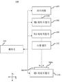
도 1은 본 발명의 일 실시예에 따른, 작업물 가공 장치를 개략적으로 도시한다.
도 2 및 도 3은 실리콘 웨이퍼의 표면에 형성된 트렌치(trenches)의 (평면도로 촬영된) 현미경 사진을 도시한다.
도 4는 각각 실리콘 웨이퍼의 표면에 형성된 교차하는 스크라이브 라인(scribe lines)의 세트를 포함하는, 레이저 가공된 피처의 (평면도로 촬영된) 현미경 사진을 도시한다.
도 5는 레이저 펄스를 상이한 펄스 반복률로 스캔된 빔 축을 따라 전파시킴으로써 실리콘 웨이퍼 내에 형성된 트렌치에서, 가공된 작업물 표면의 평균 표면 거칠기(Ra) 및 트렌치 형성 가공 동안 상이한 펄스 반복률 사이의 관계를 바이트 크기 및 플루엔스의 함수로 나타내는 그래프의 세트를 도시한다.
도 6은 특정 특징을 갖는 가공된 작업물 표면의 형성을 초래하는 실리콘 웨이퍼 내에 트렌치를 형성하는 가공 윈도우(process windows)를 나타내는 그래프의 세트를 도시한다.
도 7은 매끄럽게 가공된 작업물 표면을 생성하는(yields) 방식으로 트렌치를 형성하도록 가공된 실리콘 웨이퍼의 현미경 사진(측단면도로 촬영됨)을 도시한다.
도 8a 및 도 8b는 실리콘 웨이퍼가 실리콘 웨이퍼 내의 트렌치 균열을 형성하도록 더 가공된 후의, 도 7에 도시된 가공된 실리콘 웨이퍼의 현미경 사진(측단면도로 촬영됨)을 도시한다. 도 8a는 도 7에 도시된 트렌치의 폭을 가로지르는 도면을 도시한다. 도 8b는 도 7에 도시된 트렌치의 길이를 따르는 도면을 도시한다.
도 9a 내지 도 9d는 일부 실시예에 따른, 작업물 가공 방법을 도시한다.1 schematically shows a workpiece processing apparatus according to an embodiment of the present invention.
Figures 2 and 3 show micrographs (taken in plan) of trenches formed on the surface of a silicon wafer.
Figure 4 shows a micrograph of a laser machined feature (photographed in a top view), each containing a set of intersecting scribe lines formed on the surface of a silicon wafer.
Figure 5 shows the relationship between the average surface roughness (Ra) of the worked work surface and the different pulse repetition rates during trench formation processing in the trenches formed in the silicon wafer by propagating the laser pulses along the beam axis scanned at different pulse repetition rates, ≪ / RTI > and fluence.
Figure 6 shows a set of graphs showing process windows for forming trenches in a silicon wafer resulting in the formation of a machined workpiece surface with certain characteristics.
Figure 7 shows a micrograph (taken in side cross-section) of a silicon wafer that has been processed to form a trench in a manner that yields a smoothly machined work surface.
Figures 8a and 8b show a micrograph (taken in side cross-section) of the processed silicon wafer shown in Figure 7 after the silicon wafer is further processed to form a trench crack in the silicon wafer. FIG. 8A shows a view across the width of the trench shown in FIG. FIG. 8B shows a view along the length of the trench shown in FIG.
Figures 9A-9D illustrate a method of processing a workpiece, according to some embodiments.
첨부 도면을 참조로 예시적인 실시예가 여기에서 설명된다. 달리 명시하지 않는 한, 도면에서 구성요소, 피처(features), 요소 등의 크기, 위치 등과 이들 사이의 어느 거리는 축적대로 도시된 것은 아니고, 명료화를 위해 과장된다.Exemplary embodiments are described herein with reference to the accompanying drawings. Unless otherwise specified, the sizes, locations, etc. of components, features, elements, etc., and any distance therebetween are not shown in scale, but are exaggerated for clarity.
본원에 사용되는 용어는 예시적인 특정 실시예만을 설명하기 위함이며, 제한하고자 함이 아니다. 본원에 사용된 단수 형태인 "하나의(a, an)", 및 "그(the)"는 문맥상 달리 명확하게 지시하지 않는 한, 복수 형태도 포함하는 것으로 의도된다. 본 명세서에서 사용될 때 "포함하다" 및/또는 "포함하는"이란 용어는 서술된 피처, 정수, 단계, 동작, 요소 및/또는 구성요소의 존재를 명시하지만, 하나 이상의 다른 피처, 정수, 단계, 동작, 요소, 구성요소 및/또는 이들의 그룹의 존재 또는 추가를 배제하지 않음이 인식되어야 한다. 달리 명시되지 않는 한, 인용되는 값의 범위는 그 범위의 상한치와 하한치 둘 다는 물론, 이들 사이의 어느 하위 범위를 포함한다. 달리 지시되지 않는 한, "제1", 제2" 등과 같은 용어는 하나의 요소를 다른 요소와 구분하기 위해서만 사용된다. 예를 들어, 하나의 노드는 "제1 노드"로 칭할 수 있고, 마찬가지로 다른 노드는 "제2 노드"로 칭할 수 있으며 그 역으로도 가능하다. 본원에 사용된 섹션 제목은 오직 구조적인 목적이며, 서술되는 주제를 제한하는 것으로 해석되지 않아야 한다. The terminology used herein is for the purpose of describing particular exemplary embodiments only, and is not intended to be limiting. The singular forms " a, "and" the ", as used herein, are intended to include plural forms unless the context clearly dictates otherwise. As used herein, the terms "comprises" and / or "comprising" specify the presence of stated features, integers, steps, operations, elements and / or components but may include one or more other features, integers, And does not preclude the presence or addition of one or more other features, elements, elements, elements, and / or groups thereof. Unless otherwise specified, the range of values quoted includes both the upper and lower limits of the range, as well as any subranges therebetween. Unless otherwise indicated, terms such as "first", "second", etc. are used only to distinguish one element from another element. Other nodes may be referred to as "second nodes" and vice versa. The section headings used herein are for structural purposes only and should not be construed as limiting the described subject matter.
달리 지시되지 않는 한, "약", "대략" 등의 용어는 양, 크기, 제형(formulations), 파라미터 및 다른 수량과 특징이 정확하지 않고 정확할 필요도 없으나, 바람직한 경우, 반영 공차(reflecting tolerances), 변환 인자, 반올림, 측정 오차 등, 그리고 이 분야의 기술자에게 알려진 다른 인자에 대한 근사치이거나 및/또는 이보다 크거나 작을 수 있음을 의미한다. Unless otherwise indicated, terms such as " about ", "about ", and the like, do not necessarily imply correctness and accuracy in terms of quantity, size, formulations, parameters and other quantities and characteristics, , Conversion factor, rounding, measurement error, etc., and other factors known to those skilled in the art and / or may be greater or lesser.
"아래의(below)", "아래쪽의(beneath)", "낮은(lower)", "위의(above)" 및 "높은(upper)" 등과 같은 공간적으로 상대적인 용어는 도면에 도시된 것처럼, 하나의 요소 또는 피처와 다른 요소 또는 피처의 관계를 서술하는 설명의 용이함을 위해 본원에서 사용될 수 있다. 공간적으로 상대적인 용어가 도면에 도시된 배향에 부가하여 상이한 배향도 포괄할 수 있음을 인식해야 한다. 예를 들어, 도면에서 객체가 회전되면, 다른 요소 또는 피처 "아래의" 또는 "아래쪽"으로 서술된 요소는 다른 요소 또는 특징의 "위"로 배향될 것이다. 따라서, "아래의"란 예시적인 용어는 위 및 아래의 배향 양자를 포괄할 수 있다. 객체는 다르게 배향될 수 있고(예를 들어, 90도 회전 또는 다른 배향), 본원에서 사용되는 공간적 관련 서술자는 그에 따라 해석될 수 있다.Spatially relative terms such as "below", "beneath", "lower", "above" and "upper" May be used herein for ease of description that describes the relationship of one element or feature to another element or feature. It should be appreciated that spatially relative terms may encompass different orientations in addition to those shown in the figures. For example, when an object is rotated in the figures, elements described as "below" or "below" another element or feature will be oriented "above" another element or feature. Thus, an exemplary term "below" may encompass both orientation above and below. Objects may be oriented differently (e.g., 90 degrees rotated or other orientations), and spatial related descriptors used herein may be interpreted accordingly.
전체에 걸쳐, 유사한 부호는 유사한 요소를 지칭한다. 따라서, 동일하거나 유사한 부호는, 대응하는 도면에서 언급되거나 서술되지 않더라도, 다른 도면을 참조로 서술될 수 있다. 또한, 참조 부호로 표기되지 않은 요소도 다른 도면을 참조로 서술될 수 있다.Throughout the drawings, like reference numerals refer to like elements. Accordingly, the same or similar reference numerals can be described with reference to other figures, even if they are not mentioned or described in the corresponding drawings. Elements not represented by reference numerals may also be described with reference to other drawings.
본 개시의 사상 및 교시를 벗어나지 않고 다수의 상이한 형태 및 실시예가 가능할 수 있음이 인식될 것이고, 따라서 본 개시는 본원에 제시된 예시적인 실시예로 제한되는 것으로 해석되지 않아야 한다. 오히려, 이들 예시 및 실시예는 본 개시가 철저하고 완전하며, 이 기술분야의 기술자에게 본 개시의 범주를 전달하도록 제공된다.It will be appreciated that a number of different forms and embodiments may be possible without departing from the spirit and teachings of the disclosure, and thus the present disclosure should not be construed as limited to the exemplary embodiments set forth herein. Rather, these examples and embodiments are provided so that this disclosure will be thorough and complete, and will convey the scope of the disclosure to those skilled in the art.
1. 개요1. Overview
본원에 서술된 실시예는 일반적으로 레이저 기반 기계가공(또한, 본원에서 작업물의 레이저-가공, 레이저 가공, 또는 가장 간단하게는 "가공"으로 지칭됨)을 위한 방법 및 장치에 관한 것이다. 일반적으로, 가공은 작업물을 가열, 융해, 기화, 삭마, 균열(crack), 연마 등을 하기 위하여, 레이저 광선으로 작업물을 조사함으로써 그 전체가 또는 부분적으로 달성된다. 도시된 장치에 의해 수행될 수 있는 가공의 특정 예시는 비아 드릴링(via drilling), 스크라이빙(scribing), 다이싱(dicing), 인그레이빙(engraving) 등을 포함한다. 따라서, 가공의 결과로 작업물 상에 또는 작업물 내에 형성될 수 있는 피처는 개구부, 비아(예를 들어, 블라인드 비아, 관통 비아, 슬롯 비아), 홈, 트렌치, 스크라이브 라인, 커프(kerfs), 리세스된(recessed) 영역 등 또는 이들의 어느 조합을 포함할 수 있다.The embodiments described herein generally relate to methods and apparatus for laser-based machining (also referred to herein as laser-machining, laser machining, or, most simply, "machining" of a workpiece). Generally, machining is accomplished in whole or in part by irradiating the workpiece with a laser beam to heat, melt, vaporize, ablate, crack, grind, etc. the workpiece. Specific examples of processing that may be performed by the illustrated apparatus include via drilling, scribing, dicing, engraving, and the like. As such, features that may be formed on or in the workpiece as a result of machining may include apertures, vias (e.g., blind vias, through vias, slot vias), grooves, trenches, scribe lines, kerfs, A recessed region, etc., or any combination thereof.
가공될 수 있는 작업물은 일반적으로, 금속, 폴리머, 세라믹, 또는 이들의 어느 조합으로 특징지어질 수 있다. 가공될 수 있는 작업물의 특정 예시는 집적 회로(ICs), IC 패키지(ICPs), 발광 다이오드(LEDs), LED 패키지, 반도체 웨이퍼, 전자 또는 광학 디바이스 기판(예를 들어, Al2O3, AlN, BeO, Cu, GaAs, GaN, Ge, InP, Si, SiO2, SiC, Si1-xGex (여기서 0.0001 < x < 0.9999) 등 또는 이들의 어느 조합 또는 합금으로 형성된 기판), 플라스틱, 유리(예를 들어, 열적으로, 화학적으로, 또는 다른 방식으로 강화되거나 강화되지 않음), 석영, 사파이어, 플라스틱, 실리콘 등으로 형성된 물품을 포함한다. 따라서, 가공될 수 있는 재료는 하나 이상의 금속(예를 들어, Al, Ag, Au, Cu, Fe, In, Mg, Pt, Sn, Ti 등 또는 이들의 조합 또는 합금), 전도성 금속 산화물(예를 들어, ITO 등), 투명한 전도성 폴리머, 세라믹, 왁스(waxes), 수지, 기판 재료(예를 들어, Al2O3, AlN, BeO, Cu, GaAs, GaN, Ge, InP, Si, SiO2, SiC, Si1-xGex 등, 또는 이들의 조합 또는 합금), (예를 들어, 산화규소, 질화규소, 산질화규소 등 또는 이들의 어느 조합과 같은 중간층 유전체 구조로 사용되는) 무기 유전 재료, 로우-k(low-k) 유전 재료(예를 들어, 메틸 실세스퀴옥산 (MSQ), 하이드로겐 실세스퀴옥산(HSQ), 플루오르화 테트라에틸 오소실리케이트 (FTEOS) 등 또는 이들의 어느 조합), 유기 유전 재료(예를 들어, (도우(Dow) 사에서 제조된) 실크(SILK), 벤조시클로부텐, 노틸러스(Nautilus), (듀퐁(DuPont) 사에서 제조된) 폴리플루오로테트라에틸렌, (얼라이드 케미컬(Allied Chemical) 사에서 제조된) FLARE 등 또는 이들의 어느 조합), 유리 섬유, 폴리머 재료(폴리아미드, 폴리이미드, 폴리에스테르, 폴리아세탈, 폴리카보네이트, 변성 폴리페닐렌 에테르, 폴리부틸렌 테레프탈레이트, 폴리페닐렌 설파이드, 폴리에테르 술폰, 폴리에테르 이미드, 폴리에테르 에테르 케톤, 액정 폴리머, 아크릴로니트릴 부타디엔 스티렌 및 이들의 어느 화합물, 조성물 또는 합금) 등 또는 이들의 어느 조합을 포함한다.The workpieces that can be machined can generally be characterized as metal, polymer, ceramic, or any combination thereof. Specific examples of water that can be processed work is integrated circuits (ICs), IC package (ICPs), light emitting diodes (LEDs), LED packages, a semiconductor wafer, electronic or optical device substrate (e.g., Al 2 O 3, AlN, A substrate formed of any one of or a combination of these materials or alloys such as BeO, Cu, GaAs, GaN, Ge, InP, Si, SiO 2 , SiC, Si 1 -xGe x (where 0.0001 <x <0.9999) For example, not thermally, chemically, or otherwise strengthened or enhanced), quartz, sapphire, plastic, silicon, and the like. Thus, the material that can be processed is one or more metals (e.g., Al, Ag, Au, Cu, Fe, In, Mg, Pt, Sn, Ti, etc. or combinations or alloys thereof), conductive metal oxides g., ITO and the like), transparent conductive polymers, ceramics, waxes (waxes), resin, ceramic material (e.g., Al 2 O 3, AlN, BeO, Cu, GaAs, GaN, Ge, InP, Si, SiO 2, Inorganic dielectric material, such as SiC, Si 1-x Ge x , or the like, or a combination or alloy thereof), (for example, used as an interlayer dielectric structure such as silicon oxide, silicon nitride, silicon oxynitride, (HSQ), tetraethylorthosuccinate fluoride (FTEOS), or any combination thereof), a low k dielectric material such as methyl silsesquioxane (MSQ), hydrogen silsesquioxane (HSQ) Organic dielectric materials (such as SILK, benzocyclobutene, Nautilus, manufactured by DuPont), polyfluorene (manufactured by DuPont) FLARE, or any combination thereof), glass fibers, polymer materials (such as polyamides, polyimides, polyesters, polyacetals, polycarbonates, modified polyphenylene Polyether imide, polyether ether ketone, liquid crystal polymer, acrylonitrile butadiene styrene, and any of the compounds, compositions or alloys thereof), or any of them Combinations.
II. 시스템 - 개요II. System - Overview
도 1은 본 발명의 일 실시예에 따른, 작업물 가공 장치를 개략적으로 도시한다.1 schematically shows a workpiece processing apparatus according to an embodiment of the present invention.
도 1에 도시된 실시예를 참조하면, 작업물(102)을 가공하는 장치(100)는 레이저 펄스를 생성하는 레이저원(104), 제1 위치 지정기(106), 제2 위치 지정기(108), 제3 위치 지정기(110), 스캔 렌즈(112) 및 제어기(114)를 포함한다. 후속하는 서술을 고려하여, 장치가 제2 위치 지정기(108)를 포함하는 경우, 제1 위치 지정기(106)의 포함은 선택적임(즉, 장치(100)가 제1 위치 지정기(106)를 포함할 필요가 없음)이 인식되어야 한다. 마찬가지로, 장치가 제1 위치 지정기(106)를 포함하는 경우, 제2 위치 지정기(108)의 포함은 선택적임(즉, 장치(100)가 제2 위치 지정기(108)를 포함할 필요가 없음)이 인식되어야 한다. 마지막으로, 유사하게 제3 위치 지정기(110)의 포함이 선택적임(즉, 장치(100)가 제3 위치 지정기(108)를 포함할 필요가 없음)이 인식되어야 한다.1, an
도시되진 않았지만, 장치(100)는 레이저원(104)에 의해 생성된 레이저 펄스를 하나 이상의 빔 경로(예를 들어, 빔 경로(116))를 따라 스캔 렌즈(112)로 집속, 확장, 시준(collimate), 성형(shape), 편광, 필터링, 분할, 결합, 크롭(crop) 또는 다른 방식으로 변형, 조절(condition) 또는 지향하기 위해, 하나 이상의 광학 구성요소(예를 들어, 빔 익스팬더(beam expanders), 빔 성형기(shapers), 개구, 고조파 발생 결정(crystals), 필터, 시준기(collimators), 렌즈, 미러, 편광기, 파장판, 회절 광학 요소 등 또는 이들의 어느 조합)을 더 포함한다. 전술한 구성요소 중 하나 이상이 제공될 수 있거나, 또는 장치(100)가 미국특허 제4,912,487호, 제5,633,747호, 제5,638,267호, 제5,751,585호, 제5,847,960호, 제5,917,300호, 제6,314,473호, 제6,430,465, 제6,700,600호, 제6,706,998호, 제6,706,999호, 제6,816,294호, 제6,947,454호, 제7,019,891호, 제7,027,199호, 제7,133,182호, 제7,133,186호, 제7,133,187호, 제7,133,188호, 제7,245,412호, 제7,259,354호, 제7,611,745호, 제7,834,293호, 제8,026,158호, 제8,076,605호, 제8,158,493호, 제8,288,679호, 제8,404,998호, 제8,497,450호, 제8,648,277호, 제8,680,430호, 제8,847,113호, 제8,896,909호, 제8,928,853호, 또는 전술한 미국특허출원 공개번호 제2014/0026351호, 제2014/0197140호, 제2014/0263201호, 제2014/0263212호, 제2014/0263223호, 제2014/0312013호, 또는 독일특허 제DE102013201968B4호, 또는 국제특허출원 공개번호 제WO2009/087392호, 또는 이들의 어느 조합에 개시된 추가적인 구성요소를 더 포함할 수 있음이 더 인식될 것이고, 이들 각각은 그 전체가 본원에 참조로 통합된다.Although not shown, the
스캔 렌즈(112)를 통해 송신된 레이저 펄스는 작업물(102)로 전달되도록 빔 축을 따라 전파한다. 작업물(102)로 전달되는 레이저 펄스는 가우시안 또는 성형된(예를 들어, "탑 햇(top-hat)") 공간적 강도 프로파일을 갖는 것으로 특징지어질 수 있다. 공간적 강도 프로파일은 원형, 타원형, 직사각형, 삼각형, 육각형, 링형 등일 수 있거나 또는 임의로 성형될 수 있는, 빔 축(또는 빔 경로(106))을 따라 전파하는 레이저 펄스의 단면 형태로 더 특징지어질 수 있다. 또한, 이러한 전달된 레이저 펄스는 2 μm 내지 200 μm의 범위 내에 있는 스폿 크기로 작업물(102)에 충돌할 수 있다. 본원에서 사용되는 "스폿 크기"란 용어는 빔 축이, 전달된 레이저 펄스에 의해 가공될 작업물(102)의 영역을 횡단하는 위치(또한, "가공 장소", "가공 스폿", "스폿 위치" 또는 더 간단하게는 "스폿")에서 전달된 레이저 펄스의 직경 또는 공간적 폭을 지칭한다. 본원에서 논의의 목적으로, 스폿 크기는 빔 축으로부터 광 강도가 빔 축에서 광 강도의 1/e2로 떨어지는 곳까지의 방사 또는 횡단 거리로 측정된다. 일반적으로, 레이저 펄스의 스폿 크기는 빔 웨이스트에서 최소일 것이다. 하지만, 스폿 크기는 2 μm보다 작거나, 또는 200 μm보다 크게 생성될 수 있음이 인식될 것이다. 따라서, 작업물(102)로 전달되는 적어도 하나의 레이저 펄스는 2 μm, 3 μm, 5 μm, 7 μm, 10 μm, 15 μm, 30 μm, 35 μm, 40 μm, 45 μm, 50 μm, 55 μm, 80 μm, 100 μm, 150 μm, 200 μm 등의 미만이거나, 이를 초과하거나, 또는 이와 동일하거나 또는 이들 값 중 어느 값 사이의 스폿 크기를 가질 수 있다. 일 실시예에서, 작업물(102)로 전달되는 레이저 펄스는 25 μm 내지 60 μm의 범위 내에 있는 스폿 크기를 가질 수 있다. 다른 실시예에서, 작업물(102)로 전달되는 레이저 펄스는 35 μm 내지 50 μm의 범위 내에 있는 스폿 크기를 가질 수 있다.The laser pulses transmitted through the
A. 레이저원A. Laser source
일반적으로, 레이저원(104)은 레이저 펄스를 생성하도록 동작한다. 이처럼, 레이저원(104)은 펄스 레이저원, QCW 레이저원 또는 CW 레이저원을 포함할 수 있다. 레이저원(104)이 QCW 또는 CW 레이저원을 포함하는 경우, 레이저원(104)은 QCW 또는 CW 레이저원으로부터 출력된 레이저 방사의 빔을 시간적으로 변조하기 위한 펄스 게이팅(pulse gating) 유닛(예를 들어, 음향 광학(AO) 변조기(AOM), 빔 초퍼(beam chopper) 등)을 더 포함할 수 있다. 도시되진 않았지만, 장치(100)는 경우에 따라, 레이저원(104)에 의해 출력된 광의 파장을 변환하도록 구성된 하나 이상의 고조파 발생 결정(또한, "파장 변환 결정"으로 알려짐)을 포함할 수 있다. 따라서, 작업물(102)에 최종적으로 전달되는 레이저 펄스는 전자기 스펙트럼의 자외선(UV), 가시광선(예를 들어, 녹색), 적외선(IR), 근적외선(NIR), 단파장 IR(SWIR), 중간 파장 IR(MWIR), 또는 장파장 IR(LWIR) 범위 또는 이들의 어느 조합을 갖는 것으로 특징지어질 수 있다.Generally, the
레이저원(104)에 의해 출력되는 레이저 펄스는 30 fs 내지 500 ps의 범위 내에 있는 (즉, 광 전력 대 시간의 반치 전폭(full-width at half-maximum, FWHM)을 기초로 하는) 펄스 폭 또는 지속기간을 가질 수 있다. 하지만, 펄스 지속기간은 10 fs 보다 짧거나, 또는 500 ps보다 길게 생성될 수 있음이 인식될 것이다. 따라서, 레이저원(104)에 의해 출력되는 적어도 하나의 레이저 펄스는 10 fs, 15 fs, 30 fs, 50 fs, 75 fs, 100 fs, 150 fs, 200 fs, 300 fs, 500 fs, 700 fs, 750 fs, 800 fs, 850 fs, 900 fs, 1 ps, 2 ps, 3 ps, 4 ps, 5 ps, 7 ps, 10 ps, 15 ps, 25 ps, 50 ps, 75 ps, 100 ps, 200 ps, 500 ps 등의 미만이거나, 이를 초과하거나, 또는 이에 동일하거나, 또는 이들 값 중 어느 것 사이의 펄스 지속기간을 가질 수 있다. 일 실시예에서, 레이저원(104)에 의해 출력되는 레이저 펄스는 10 fs 내지 1 ps의 범위 내에 있는 펄스 지속기간을 갖는다. 다른 실시예에서, 레이저원(104)에 의해 출력되는 레이저 펄스는 500 fs 내지 900 fs의 범위 내에 있는 펄스 지속기간을 갖는다. The laser pulse output by the
레이저원(104)에 의해 출력되는 레이저 펄스는 100 mW 내지 50 kW의 범위 내에 있는 평균 전력을 가질 수 있다. 하지만, 평균 전력은 100 mW보다 작거나, 50 kW 보다 높게 생성될 수 있음이 인식될 것이다. 따라서, 레이저원(104)에 의해 출력되는 레이저 펄스는 100 mW, 300 mW, 500 mW, 800 mW, 1 W, 2 W, 3 W, 4 W, 5 W, 6 W, 7 W, 10 W, 15 W, 25 W, 30 W, 50 W, 60 W, 100 W, 150 W, 200 W, 250 W, 500 W, 2 kW, 3 kW, 20 kW, 50 kW 등의 이상이거나 또는 이들 값 중 어느 것 사이의 평균 전력을 가질 수 있다. The laser pulse output by the
레이저 펄스는 레이저원(104)에 의해 5 kHz 내지 1 GHz의 범위 내에 있는 펄스 반복률로 출력될 수 있다. 하지만, 펄스 반복률은 5 kHz 미만이거나, 또는 1 GHz를 초과할 수 있음이 인식될 것이다. 따라서, 레이저 펄스는 레이저원(104)에 의해, 5 kHz, 50 kHz, 100 kHz, 250 kHz, 500 kHz, 800 kHz, 900 kHz, 1 MHz, 1.5 MHz, 1.8 MHz, 1.9 MHz, 2 MHz, 2.5 MHz, 3 MHz, 4 MHz, 5 MHz, 10 MHz, 20 MHz, 50 MHz, 70 MHz, 100 MHz, 150 MHz, 200 MHz, 250 MHz, 300 MHz, 350 MHz, 500 MHz, 550 MHz, 700 MHz, 900 MHz, 2 GHz, 10 GHz 등의 미만이거나, 이를 초과하거나, 또는 이와 동일하거나, 또는 이들 값 중 어느 것 사이의 펄스 반복률로 출력될 수 있다. 일부 실시예에서, 펄스 반복률은 1.5 MHz 내지 10 MHz의 범위 내에 있을 수 있다.The laser pulse can be output by the
파장, 펄스 지속기간, 평균 전력 및 펄스 반복률에 부가하여, 작업물(102)로 전달된 레이저 펄스는 하나 이상의 바람직한 특징을 갖는 하나 이상의 피처를 형성하기 위하여, 가공 스폿에서 작업물(102) 또는 그의 구성요소를 가공하는데 충분한 (W/cm2로 측정되는) 광 강도와 (J/cm2로 측정되는) 플루엔스(fluence) 등으로 작업물(102)에 방사하도록 하나 이상의 다른 파라미터를 기초로 선택될 수 있는 펄스 에너지, 피크 전력 등과 같은 하나 이상의 다른 특징에 의해 특징지어질 수 있다. 이러한 다른 파라미터의 예시는 파장, 펄스 지속기간, 평균 전력 및 펄스 반복률 뿐만 아니라, 작업물(102)의 재료 특성, 바이트 크기, 바람직한 가공 처리량 등 또는 이들의 어느 조합과 같은 전술한 특징 중 하나 이상을 포함한다. 본원에서 사용된 "바이트 크기"란 용어는 연속적으로 전달된 레이저 펄스에 의해 조사되는 스폿 면적 사이의 중심간 거리를 지칭한다. In addition to the wavelength, pulse duration, average power, and pulse repetition rate, the laser pulses delivered to the
예를 들어, 작업물(102)로 전달되는 레이저 펄스는 1 μJ 내지 20 μJ의 범위 내에 있는 펄스 에너지를 가질 수 있다. 일 실시예에서, 어느 전달된 레이저 펄스는 2 μJ 내지 10 μJ의 범위 내에 있는 펄스 에너지를 가질 수 있다. 다른 실시예에서, 어느 전달된 레이저 펄스는 3 μJ 내지 6 μJ의 범위 내에 있는 펄스 에너지를 가질 수 있다. 하지만, 전달된 레이저 펄스의 펄스 에너지는 1 μJ 미만이거나, 20 μJ를 초과할 수 있음이 인식될 것이다. 다른 예시에서, 작업물(102)로 전달된 레이저 펄스는 1 μJ 내지 20 μJ의 범위 내에 있는 플루엔스를 가질 수 있다. 일 실시예에서, 어느 전달된 레이저 펄스는 2 μJ 내지 10 μJ의 범위 내에 있는 펄스 에너지를 가질 수 있다. 다른 실시예에서, 어느 전달된 레이저 펄스는 2 μJ to 6 μJ의 범위 내에 있는 펄스 에너지를 가질 수 있다. 하지만, 전달된 레이저 펄스의 펄스 에너지는 1 μJ 미만이거나, 20 μJ를 초과할 수 있음이 인식될 것이다.For example, the laser pulse delivered to the
레이저 타입의 예시들은 레이저원(104)이 기체 레이저(예를 들어, 이산화탄소 레이어, 일산화탄소 레이저, 엑시머 레이저 등), 고체 상태 레이저(예를 들어, Nd:YAG 레이저 등), 로드(rod) 레이저, 파이버(fiber) 레이저, 광결정 로드/파이버 레이저(photonic crystal rod/fiber lasers), 수동형 모드 록 고체 상태 벌크 또는 파이버 레이저(passively mode-locked solid-state bulk or fiber lasers), 다이(dye) 레이저, 모드-록(mode-locked) 다이오드 레이저, 펄스 레이저(예를 들어, ms-, ns-, ps-, fs-펄스 레이저), CW레이저, QCW레이저 등 또는 이들의 어느 조합으로서 특징지어질 수 있다. 레이저원(104)으로서 제공될 수 있는 레이저원의 특정 예시는 EOLITE 사에서 제조된 BOREAS, HEGOA, SIROCCO 또는 CHINOOK 레이저 시리즈; PYROPHOTONICS 사에서 제조된 PYROFLEX 레이저 시리즈; COHERENT 사에서 제조된 PALADIN Advanced 355 또는 DIAMOND 레이저 시리즈; TRUMPF 사에서 제조된 TRUFLOW 레이저 시리즈(예를 들어, TRUFLOW 2000, 2700, 3200, 3600, 4000, 5000, 6000, 7000, 8000, 10000, 12000, 15000, 20000), 또는 TRUDISK-, TRUPULSE-, TRUDIODE-, TRUFIBER-, 또는 TRUMICRO 레이저 시리즈; IMRA AMERICA 사에서 제조된 FCPA μJEWEL 또는 FEMTOLITE 레이저 시리즈; AMPLITUDE SYSTEMES 사에서 제조된 TANGERINE 및 SATSUMA 시리즈 레이저( 및 MIKAN 및 T-PULSE 시리즈 발진기); IPG PHOTONICS 사에서 제조된 CL-, CLPF-, CLPN-, CLPNT-, CLT-, ELM-, ELPF-, ELPN-, ELPP-, ELR-, ELS-, FLPN-, FLPNT-, FLT-, GLPF-, GLPN-, GLR-, HLPN-, HLPP-, RFL-, TLM-, TLPN-, TLR-, ULPN-, ULR-, VLM-, VLPN-, YLM-, YLPF-, YLPN-, YLPP-, YLR-, YLS-, FLPM-, FLPMT-, DLM-, BLM-, 또는 DLR- 레이저 시리즈(예를 들어, GPLN-100-M, GPLN-500-QCW, GPLN-500-M, GPLN-500-R, GPLN-2000-S 등을 포함함) 등 또는 이들의 어느 조합과 같은 하나 이상의 레이저원을 포함한다.Examples of laser types are those in which the
B. 제1 위치 지정기B. First Positioner
제1 위치 지정기(106)는 빔 경로(116)에 배치되고, 스캔 렌즈(112)에 대한 빔 경로(116)의 이동을, 따라서 작업물(102)에 대한 빔 축의 이동을 제공하도록, 레이저원(104)에 의해 생성된 레이저 펄스를 회절, 반사, 굴절 등 또는 이들의 어느 조합을 하도록 동작한다. 일반적으로, 제1 위치 지정기(106)는 작업물(102)에 대해 X 및 Y축(또는 방향)을 따른 빔 축의 이동을 제공하도록 구성된다. 도시되진 않았지만, Y축(또는 Y 방향)은 도시된 X 및 Z축(또는 방향)에 직교하는 축(또는 방향)을 지칭하는 것으로 이해될 것이다. The
제1 위치 지정기(106)에 의해 제공된 작업물(102)에 대한 빔 축의 이동은 일반적으로, 가공 스폿이 X 및 Y 방향으로 0.01 mm 내지 4.0 mm 사이로 연장하는 제1 스캔 필드 또는 "제1 스캐닝 범위" 내로 스캔, 이동 또는 다른 방식으로 위치 지정될 수 있도록 제한된다. 하지만, 제1 스캐닝 범위는 X 또는 Y 방향 중 어느 방향으로도 (예를 들어, 제1 위치 지정기(106)의 구성, 빔 경로(116)를 따른 제1 위치 지정기(106)의 위치, 제1 위치 지정기(106)에 입사하는 레이저 펄스의 빔 크기, 스폿 크기 등과 같은 하나 이상의 인자에 의존하여) 0.01 mm 미만으로 또는 4.0 mm를 초과하여 연장할 수 있음이 인식될 것이다. 따라서, 제1 스캐닝 범위는 X 및 Y 방향 중 어느 방향으로도, 0.04 mm, 0.1 mm, 0.5 mm, 1.0 mm, 1.4 mm, 1.5 mm, 1.8 mm, 2 mm, 2.5 mm, 3.0 mm, 3.5 mm, 4.0 mm, 4.2 mm 등 이상의 또는 이들 값 중 어느 값 사이의 거리만큼 연장할 수 있다. 본원에서 사용된 "빔 크기"란 용어는 레이저 펄스의 직경 또는 폭을 지칭하고, 빔 축으로부터, 광 강도가 빔 축에서 광 강도의 1/e2로 떨어지는 곳까지의 방사 또는 횡단 거리로 측정될 수 있다. Movement of the beam axis relative to the
일반적으로, 제1 위치 지정기(106)가 빔 축을 이동시킬 수 있고, 따라서 가공 스폿을 위치시킬 수 있는 대역폭(즉, 제1 위치 지정 대역폭)은 50 kHz(또는 그 즈음) 내지 10 MHz(또는 그 즈음)의 범위 내에 있다. 따라서, 제1 위치 지정기(106)는 20 μs(또는 그 즈음) 당 하나의 스폿 위치 내지 0.1 μs(또는 그 즈음) 당 하나의 스폿 위치의 범위 내에 있는 위치 지정 속도(제1 위치 지정 대역폭으로부터 안출됨)로 제1 스캐닝 범위 내의 어느 위치에 가공 스폿을 위치시킬 수 있다. 위치 지정 속도의 역수는 본원에서 "위치 지정 주기"로 지칭되고, 제1 스캐닝 범위 내의 일 위치로부터 제1 스캐닝 범위 내의 다른 어느 위치로 가공 스폿의 위치를 변경하는 데 필요한 시간 주기로 지칭된다. 따라서, 제1 위치 지정기(106)는 20 μs(또는 그 즈음) 내지 0.1 μs(또는 그 즈음)의 범위 내에 있는 위치 지정 주기에 의해 특징지어질 수 있다. 일 실시예에서, 제1 위치 지정 대역폭은 100 kHz(또는 그 즈음) 내지 2 MHz(또는 그 즈음)의 범위 내에 있다. 예를 들어, 제1 위치 지정 대역폭은 1 MHz(또는 그 즈음)이다. Generally, the
제1 위치 지정기(106)는 초소형 정밀 기계 시스템(micro-electro-mechanical-system, MEMS) 미러 또는 미러 어레이, AO 편향기(AOD) 시스템, 전자 광학 편향기(EOD) 시스템, 압전 액추에이터, 전왜 액추에이터(electrostrictive actuator), 음성 코일 액추에이터 등을 포함하는 고속 조향 미러(FSM) 요소 등 또는 이들의 어느 조합으로 제공될 수 있다. 일 실시예에서, 제1 위치 지정기(106)는 적어도 하나의(예를 들어, 한 개, 두 개 등) 단일 요소(single-element) AOD 시스템, 적어도 하나의(예를 들어, 한 개, 두 개 등) 위상 어레이 AOD 시스템 등 또는 이들의 어느 조합을 포함하는 AOD 시스템으로서 제공된다. AOD 시스템 양자는 결정질 Ge, PbMoO4, 또는 TeO2, 유리질 SiO2, 석영, As2S3 등과 같은 재료로 형성된 AO 셀을 포함하지만, 전자는 AO 셀에 음향적으로 연결된 단일 초음파 변환기(ultrasonic transducer)를 포함하는 한편, 후자는 보통 AO 셀에 음향적으로 연결된 적어도 두 개의 초음파 변환기 요소의 위상 어레이를 포함한다.The
AOD 시스템 중 어느 것이라도 빔 경로(116)를 편향시킴으로써, (예를 들어, 단일 방향을 따른 빔 축의 이동을 제공하도록 구성된) 단일 축 AOD 시스템, 또는 (예를 들어, 다중 방향, 예를 들어, X 및 Y 방향을 따른 빔 축의 이동을 제공하도록 구성된) 다중 축 AOD 시스템으로서 제공될 수 있다. 일반적으로, 다중 축 AOD 시스템은 다중 셀 시스템 또는 단일 셀 시스템으로서 제공될 수 있다. 다중 셀, 다중 축 시스템은 통상적으로, 상이한 축을 따른 빔 축의 이동을 제공하도록 각각 구성된 다수의 AOD 시스템들을 포함한다. 예를 들어, 다중 셀, 다중 축 시스템은 X 방향을 따른 빔 축의 이동을 제공하도록 구성된 (예를 들어, "X축 AOD 시스템") 제1 AOD 시스템(예를 들어, 단일 요소 또는 위상 어레이 AOD 시스템), 및 Y 방향을 따른 빔 축의 이동을 제공하도록 구성된(예를 들어, "Y축 AOD 시스템") 제2 AOD 시스템(예를 들어, 단일 요소 또는 위상 어레이 AOD 시스템)을 포함할 수 있다. 단일 셀, 다중 축 시스템(예를 들어, "X/Y 축 AOD 시스템")은 통상적으로, X 및 Y 방향을 따른 빔 축의 이동을 제공하도록 구성된 단일 AOD 시스템을 포함한다. 예를 들어, 단일 셀 시스템은 공통 AOD 셀의 상이한 평면, 면(facets), 측면(sides) 등에 음향 연결된 적어도 두 개의 초음파 변환기 요소를 포함할 수 있다.A single-axis AOD system (e.g., configured to provide movement of the beam axis along a single direction), or a single-axis AOD system (e.g., multiple directions, e.g., Axis AOD system configured to provide movement of the beam axis along the X and Y directions). In general, a multi-axis AOD system may be provided as a multi-cell system or a single-cell system. Multi-cell, multi-axis systems typically include multiple AOD systems each configured to provide movement of the beam axis along different axes. For example, a multi-cell, multi-axis system may include a first AOD system (e.g., a single element or phased array AOD system) configured to provide movement of a beam axis along the X direction (e.g., ), And a second AOD system (e.g., a single element or phased array AOD system) configured to provide movement of the beam axis along the Y direction (e.g., a "Y axis AOD system"). Single-cell, multi-axis systems (e.g., "X / Y axis AOD systems") typically include a single AOD system configured to provide movement of the beam axis along the X and Y directions. For example, a single cell system may include at least two ultrasonic transducer elements acoustically connected to different planes, facets, sides, etc. of a common AOD cell.
C. 제2 위치 지정기C. Second Positioner
제1 위치 지정기(106)와 유사하게, 제2 위치 지정기(108)는 빔 경로(116)에 배치되고, 스캔 렌즈(112)에 대한 빔 경로(116)의 이동을 통해 작업물(102)에 대한 (예를 들어, X 및 Y 방향을 따른) 빔 축의 이동을 제공하기 위하여, 레이저원(104)에 의해 생성되고 제1 위치 지정기(106)에 의해 통과된 레이저 펄스를 회절, 반사, 굴절 등 또는 이들의 어느 조합으로 처리하도록 동작한다. 제2 위치 지정기(108)에 의해 제공된, 작업물(102)에 대한 빔 축의 이동은 일반적으로, 가공 스폿이 제2 스캔 필드 내에 또는, 제1 스캐닝 범위보다 큰 면적에 걸쳐, X 및/또는 Y 방향으로 연장하는 "스캐닝 범위" 내에서 스캔, 이동 또는 다른 방식으로 위치 지정될 수 있도록 제한된다. 본원에 서술된 구성을 고려하여, 제1 위치 지정기(106)에 의해 주어진 빔 축의 이동은 제2 위치 지정기(108)에 의해 제공된 빔 축의 이동에 겹쳐질 수 있음이 인식되어야 한다. 따라서, 제2 위치 지정기(108)는 제2 스캐닝 범위 내의 제1 스캐닝 범위를 스캔하도록 동작한다.Similar to the
일 실시예에서, 제2 스캐닝 범위는 X 및/또는 Y 방향으로 1 mm 내지 50 mm만큼 연장한다. 하지만, 제2 위치 지정기(108)는 제2 스캐닝 범위가 X 또는 Y 방향 중 어느 방향으로 1 mm 미만 또는 50 mm를 초과하여 연장하도록 구성될 수 있음이 인식될 것이다. 따라서, 일부 실시예에서, 제2 스캐닝 범위(예를 들어, X 또는 Y 방향 또는 다른 방식으로)의 최대 치수는 작업물(102)에 형성될 피처(예를 들어, 비아, 트렌치, 스크라이브 라인, 리세스된 영역, 전도성 트레이스 등)의 (X-Y 평면에서 측정됨) 대응하는 최대 치수 이상일 수 있다. 하지만, 다른 실시예에서, 제2 스캐닝 범위의 최대 치수는 형성될 피처의 최대 치수 미만일 수 있다.In one embodiment, the second scanning range extends from 1 mm to 50 mm in the X and / or Y direction. However, it will be appreciated that the
일반적으로, 제2 위치 지정기(108)가 빔 축을 이동시킬 수 있는, 따라서 가공을 위치시킬 수 있는(따라서, 제2 스캐닝 범위 내에서 제1 스캐닝 범위를 스캔할 수 있는) 대역폭(즉, 제2 위치 지정 대역폭)은 제1 위치 지정 대역폭보다 작다. 일 실시예에서, 제2 위치 지정 대역폭은 900 Hz 내지 5 kHz 범위 내에 있다. 다른 실시예에서, 제1 위치 지정 대역폭은 2 kHz 내지 3 kHz 범위 내(예를 들어, 약 2.5 kHz)에 있다. 예를 들어, 제2 위치 지정기(108)는 하나의 검류계 미러 구성요소가 작업물(102)에 대해 X 방향을 따른 빔 축의 이동을 제공하도록 배열되고, 다른 검류계 미러 구성요소가 작업물(102)에 대해 Y 방향을 따른 빔 축의 이동을 제공하도록 배열된 두 개의 검류계 미러 구성요소를 포함하는 검류계 미러 시스템으로서 제공된다. 하지만, 다른 실시예에서, 제2 위치 지정기(108)는 회전하는 다각형 미러 시스템 등으로서 제공될 수 있다. 따라서, 제2 위치 지정기(108) 및 제1 위치 지정기(106)의 특정 구성에 의존하여, 제2 위치 지정 대역폭은 제1 위치 지정 대역폭 이상일 수 있음이 인식될 것이다.In general, the
D. 제3 위치 지정기D. Third Positioner
제3 위치 지정기(110)는 스캔 렌즈(112)에 대한 작업물(102)의 이동, 따라서 빔 축에 대한 작업물(102)의 이동을 제공하도록 동작한다. 빔 축에 대한 작업물(102)의 이동은 일반적으로, 가공 스폿이 제2 스캐닝 범위를 초과하는 면적에 걸쳐 X 및/또는 Y 방향으로 연장하는 제3 스캔 필드 또는 "스캐닝 범위" 내에서 스캔, 이동 또는 다른 방식으로 위치될 수 있도록 제한된다. 일 실시예에서, 제3 스캐닝 범위는 X 및/또는 Y 방향으로 25 mm 내지 2 m만큼 연장한다. 다른 실시예에서, 제2 스캐닝 범위는 X 및/또는 Y 방향으로 0.5 m 내지 1.5 m만큼 연장한다. 일반적으로, (예를 들어, X 또는 Y 방향 또는 다른 방식으로) 제3 스캐닝 범위의 최대 치수는 작업물(102)에 형성될 어느 피처의 (X-Y 평면에서 측정된) 대응하는 최대 치수 이상일 것이다. 경우에 따라, 제3 위치 지정기(110)는 빔 축에 대해 작업물(102)을 (예를 들어, 1 mm 내지 50 mm의 범위에 걸쳐) Z 방향으로 연장하는 스캐닝 범위 내로 이동시키도록 구성될 수 있다. 따라서, 제3 스캐닝 범위는 X, Y 및/또는 Z 방향을 따라 연장할 수 있다.The
본원에 서술된 구성을 고려하여, 제1 위치 지정기(106) 및/또는 제2 위치 지정기(108)에 의해 제공된 빔 축의 이동이 제3 위치 지정기(110)에 의해 제공된 작업물(102)의 이동에 의해 겹칠 수 있음이 인식되어야 한다. 따라서, 제3 위치 지정기(110)는 제3 스캐닝 범위 내에서 제1 스캐닝 범위 및/또는 제2 스캐닝 범위를 스캔하도록 동작한다. 일반적으로, 제3 위치 지정기(110)가 가공 스폿을 위치시킬 수 있는(따라서, 제3 스캐닝 범위 내에서 제1 및/또는 제2 스캐닝 범위를 스캔할 수 있는) 대역폭(즉, 제3 위치 지정 대역폭)은 제2 위치 지정 대역폭 미만(예를 들어, 10 Hz, 또는 그 즈음, 또는 그 미만)이다.Considering the configuration described herein, movement of the beam axis provided by the
일 실시예에서, 제3 위치 지정기(110)는 (예를 들어, 각각 X, Y 및/또는 Z 방향을 따라 작업물(102)에 대한 선형 이동(translational) 움직임을 제공할 수 있는) 하나 이상의 선형 스테이지, (예를 들어, 각각 X, Y 및/또는 Z 방향에 평행한 축에 대해 작업물(102)에 대한 회전 이동을 제공할 수 있는) 하나 이상의 회전형 스테이지 등, 또는 이들의 어느 조합으로 제공된다. 일 실시예에서, 제3 위치 지정기(110)는 작업물(102)을 X 방향을 따라 이동시키는 X 스테이지, 및 작업물(102)을 Y 방향을 따라 이동시키기 위해 X 스테이지에 의해 지지되는 (따라서, X 스테이지에 의해 X 방향을 따라 이동 가능한) Y 스테이지를 포함한다. 도시되진 않았지만, 장치(100)는 작업물(102)이 클램핑, 고정, 유지(held), 채움(secured) 또는 다른 방식으로 지지될 수 있는, 제3 위치 지정기(110)에 연결된 선택적인 척(chuck)을 포함할 수 있다. 도시되진 않았지만, 장치(100)는 제3 위치 지정기(110)를 지지하는 선택적인 베이스(base)를 더 포함할 수 있다.In one embodiment, the
따라서 앞서 서술된 바와 같이, 장치(100)는 소위 "스택형(stacked)" 위치 지정 시스템을 채용하고, 이 시스템에서 제1 위치 지정기(106), 제2 위치 지정기(108), 스캔 렌즈(112) 등과 같은 구성요소의 위치는 제3 위치 지정기(110)를 통해 이동되는 작업물(102)에 대해 장치(100) 내에서 (예를 들어, 이 기술분야에서 알려진 바와 같이 하나 이상의 지지부, 프레임 등을 통해) 정적으로 유지된다. 다른 실시예에서, 제3 위치 지정기(110)는 제1 위치 지정기(106), 제2 위치 지정기(108), 스캔 렌즈(112) 등과 같은 하나 이상의 구성요소를 이동시키도록 배열 및 구성될 수 있고, 작업물(102)은 정적으로 유지될 수 있다. 또 다른 실시예에서, 장치(100)는 제1 위치 지정기(106), 제2 위치 지정기(108), 스캔 렌즈(112) 등과 같은 하나 이상의 구성요소가 하나 이상의 선형 또는 회전형 스테이지에 의해 운반되는 분할 축(split-axis) 위치 지정 시스템, 및 작업물(102)을 이동시키도록 배열 및 구성된 하나 이상의 선형 또는 회전형 스테이지를 채용할 수 있다. 따라서, 제3 위치 지정기(110)는 작업물(102)의 이동뿐만 아니라, 제1 위치 지정기(106), 제2 위치 지정기(108), 스캔 렌즈(112) 등 중 하나 이상의 이동을 제공한다. 장치(100)에 유리하게 또는 이롭게 채용될 수 있는 분할 축 위치 지정 시스템의 일부 예시는 각각 그 전체가 본원에 참조로 통합되는, 미국특허번호 제5,751,585호, 제5,798,927호, 제5,847,960호, 제6,706,999호, 제7,605,343호, 제8,680,430호, 제8,847,113호, 또는 미국특허출원 공개번호 제2014/0083983호, 또는 이들의 어느 조합에 개시된 것 중 어느 것이라도 포함한다. Thus, as described above, the
다른 실시예에서, 제1 위치 지정기(106), 제2 위치 지정기(108), 스캔 렌즈(112) 등과 같은 하나 이상의 구성요소는 관절이 있는 다중 축 로봇암(예를 들어, 2-, 3-, 4-, 5-, 또는 6-축 암)에 의해 운반될 수 있다. 이러한 실시예에서, 제2 위치 지정기(108) 및/또는 스캔 렌즈(112)는 경우에 따라, 로봇 암의 엔드 이펙터(end effector)에 의해 운반될 수 있다. 또 다른 실시예에서, 작업물(102)은 관절이 있는 다중 축 로봇 암의 엔드 이펙터 상에 직접(즉, 제3 위치 지정기(110) 없이) 탑재될 수 있다. 또 다른 실시예에서, 제3 위치 지정기(110)는 관절이 있는 다중 축 로봇 암의 엔드 이펙터 상에 탑재될 수 있다.In another embodiment, one or more components, such as
D. 스캔 렌즈D. Scan Lens
(예를 들어, 단순 렌즈(simple lens) 또는 복합 렌즈로 제공되는) 스캔 렌즈(112)는 통상적으로 바람직한 가공 위치에 위치될 수 있는 빔 웨이스트(beam waist)를 생성하기 위해, 빔 경로를 따라 지향된 레이저 에너지를 집속하도록 일반적으로 구성된다. 스캔 렌즈(112)는 f-세타 렌즈(f-theta lens), 텔레센트릭 렌즈, 액시콘 렌즈(axicon lens)(이 경우, 빔 축을 따라 서로 이격된 복수의 가공 스폿을 생성하는 일련의 빔 웨이스트가 생성됨), 등 또는 이들의 어느 조합으로 제공될 수 있다. The scan lens 112 (provided, for example, as a simple lens or a composite lens) is oriented along the beam path to create a beam waist, which can typically be positioned at the desired working position. Lt; RTI ID = 0.0 > laser energy. ≪ / RTI > The
E. 제어기E. Controller
일반적으로, 제어기(114)는 (예를 들어, USB, 이더넷, 파이어와이어(Firewire), Wi-Fi, RFID, NFC, 블루투스, Li-Fi 등 또는 이들의 어느 조합과 같은 하나 이상의 유선 또는 무선 통신 링크들을 통해) 레이저원(104), 제1 위치 지정기(106), 제2 위치 지정기(108), 제3 위치 지정기(110), 렌즈 액추에이터(lens actuator) 등과 같은 장치(100)의 하나 이상의 구성요소에 통신 가능하게 연결되며, 따라서, 이 구성요소는 제어기(114)에 의해 출력된 하나 이상의 제어 신호에 응답하여 동작한다.In general, the
예를 들어, 제어기(114)는 작업물(102) 내의 궤적(또한, 본원에서 "가공 궤적"으로 지칭됨)을 따라 가공 스폿과 작업물(102) 사이의 상대적 이동을 야기하기 위해 가공 스폿과 작업물 사이의 상대적 이동을 제공하도록, 제1 위치 지정기(106), 제2 위치 지정기(108) 또는 제3 위치 지정기(110)의 동작을 제어할 수 있다. 이들 위치 지정기 중 어느 두 개 또는 이들 위치 지정기 중 세 개 모두, 두 개의 위치 지정기(예를 들어, 제1 위치 지정기(106)와 제2 위치 지정기(108), 제1 위치 지정기(106)와 제3 위치 지정기(110), 또는 제2 위치 지정기(108)와 제3 위치 지정기(110)) 또는 세 개의 위치 지정기 모두가 가공 스폿과 작업물(102) 사이의 상대적 이동을 동시에 제공하도록(이를 통해, 빔 축과 작업물 사이에 "복합 상대적 이동(compound relative movement)"을 제공하도록) 제어될 수 있다. 물론, 언제라도, 가공 스폿과 작업물(102) 사이의 상대적 이동을 제공하기 위해(이를 통해, 빔 축과 작업물 사이의 "비-복합 상대적 이동"을 제공함으로써) 하나의 위치 지정기(예를 들어, 제1 위치 지정기(106), 제2 위치 지정기(108) 또는 제3 위치 지정기(110)) 만을 제어하는 것이 가능할 수 있다. 복합 또는 비복합 상대적 이동을 지시하기 위한 제어 신호는 사전 계산될 수 있거나, 다른 방식으로 실시간으로 결정될 수 있다.For example, the
일반적으로, 제어기(114)는 명령을 실행할 때 전술한 제어 신호를 생성하도록 구성된 하나 이상의 프로세서를 포함한다. 프로세서는 명령을 실행하도록 구성된 (예를 들어, 하나 이상의 범용 컴퓨터 프로세서, 마이크로프로세서, 디지털 신호 프로세서 등 또는 이들의 어느 조합을 포함하는) 프로그램 가능(programmable) 프로세서로 제공될 수 있다. 프로세서(들)에 의해 실행 가능한 명령은 소프트웨어, 펌웨어 등, 또는 PLD(programmable logic devices), FPGA(field-programmable gate arrays), FPOA(field-programmable object arrays), ASIC(application-specific integrated circuits) - 디지털, 아날로그 및 혼합된 아날로그/디지털 회로를 포함함 - 등, 또는 이들의 어느 조합을 포함하는 어느 적합한 회로의 형태로 구현될 수 있다. 명령의 실행은 디바이스 내에서 또는 디바이스의 네트워크를 통해, 하나의 프로세서 상에서 수행되거나, 프로세서 사이에 분산되거나, 프로세서를 통해 병렬로 이루어지는 등, 또는 이들의 조합으로 될 수 있다.In general, the
일 실시예에서, 제어기(114)는 (예를 들어, 하나 이상의 유선 또는 무선 통신 링크를 통해) 프로세서에 의해 액세스 가능한 컴퓨터 메모리와 같은 유형 매체를 포함한다. 본원에 사용된 "컴퓨터 메모리"는 자기 매체(예를 들어, 자기 테이프, 하드 디스크 드라이브 등), 광디스크, 휘발성 또는 비휘발성 반도체 메모리(예를 들어, RAM, ROM, NAND형 플래쉬 메모리, NOR형 플래쉬 메모리, SONOS 메모리 등) 등을 포함하고, 로컬로, 원격으로(예를 들어, 네트워크를 통해), 또는 이들의 조합으로 액세스될 수 있다. 일반적으로, 명령은 본원에 제공된 서술로부터 기술자에게 쉽게 창시될(authored) 수 있는 예를 들어, C, C++, Visual Basic, Java, Python, Tel, Perl, Scheme, Ruby 등으로 기록될 수 있는 컴퓨터 소프트웨어(예를 들어, 실행 가능한 코드, 파일, 명령어 등, 라이브러리 파일 등)으로 저장될 수 있다. 컴퓨터 소프트웨어는 주로 컴퓨터 메모리에 의해 전달되는 하나 이상의 데이터 구조로 저장된다.In one embodiment,
도시되진 않았지만, 하나 이상의 드라이버(예를 들어, RF 드라이버, 서보 드라이버, 라인 드라이버, 전원 등)은 레이저원(104), 제1 빔 위치 지정기(106), 제2 위치 지정기(108), 제3 위치 지정기(110), 렌즈 액추에이터 등과 같은 하나 이상의 구성요소의 입력에 통신 가능하게 연결될 수 있다. 일 실시예에서, 각 드라이버는 통상적으로, 제어기(114)가 통신 가능하게 연결되는 입력을 포함하고 따라서, 제어기(114)는 장치(100)의 하나 이상의 구성요소와 연관된 하나 이상의 드라이버의 입력(들)로 송신될 수 있는 하나 이상의 제어 신호(예를 들어, 트리거 신호 등)을 생성하도록 동작한다. 따라서, 레이저원(104), 제1 위치 지정기(106), 제2 위치 지정기(108), 제3 위치 지정기(110), 렌즈 액추에이터 등과 같은 구성요소는 제어기(114)에 의해 생성된 제어 신호에 응답한다.Although not shown, one or more drivers (e.g., an RF driver, a servo driver, a line driver, a power supply, etc.) may include a
다른 실시예에서, 도시되진 않았지만 하나 이상의 추가적인 제어기(예를 들어, 구성요소 특정 제어기)는 경우에 따라, 레이저원(104), 제1 위치 지정기(106), 제2 위치 지정기(108), 제3 위치 지정기(110), 렌즈 액추에이터 등과 같은 구성요소에 통신 가능하게 연결된 드라이버(따라서, 구성요소와 연관된)의 입력에 통신 가능하게 연결될 수 있다. 이 실시예에서, 각 구성요소 특정 제어기는 제어기(114)에 통신 가능하게 연결될 수 있고, 제어기(114)로부터 수신된 하나 이상의 제어 신호에 응답하여, 이후에 통신 가능하게 연결된 드라이버(들)의 입력(들)으로 송신될 수 있는 하나 이상의 제어 신호(예를 들어, 트리거 신호 등)을 생성하도록 동작할 수 있다. 이 실시예에서, 구성요소 특정 제어기는 제어기(114)에 대해 서술된 것과 유사하게 구성될 수 있다.In another embodiment, although not shown, one or more additional controllers (e.g., component specific controllers) may include a
하나 이상의 구성요소 특정 제어기가 제공되는 다른 실시예에서, 하나의 구성요소(예를 들어, 레이저원(104))와 연관된 구성요소 특정 제어기는 하나의 구성요소(예를 들어, 빔 위치 지정기(106) 등)와 연관된 구성요소 특정 제어기에 통신 가능하게 연결될 수 있다. 이 실시예에서, 구성요소 특정 제어기 중 하나 이상은 하나 이상의 다른 구성요소 특정 제어기로부터 수신된 하나 이상의 제어 신호에 응답하여 하나 이상의 제어 신호(예를 들어, 트리거 신호 등)을 생성하도록 동작할 수 있다.In another embodiment where one or more component specific controllers are provided, the component specific controller associated with one component (e.g., laser source 104) may be a component (e.g., a
III. 작업물 재료의 제거에 대한 실험 결과III. Experimental results on the removal of work material
일부 실시예에 따라, 그리고 아래에서 더 상세히 논의되는 바와 같이, 장치(100)는 하나 이상의 피처(예를 들어, 개구부, 슬롯, 비아, 홈, 트렌치, 스크라이브 라인, 커프, 리세스된 영역 등 또는 이들의 어느 조합)를 형성하기 위하여, 작업물(102)의 일부를 제거함으로써 작업물(102)을 가공하도록 구성된 레이저원(104)을 구비한다. 가공 결과로 생성된 표면은 이하에서 "가공된 작업물 표면"으로 지칭되며, 측벽, 바닥 표면 등 또는 어느 부분 또는 이들의 조합을 포함할 수 있다. 이들 실시예에서, 재료는 초단 펄스 지속기간(ultrashort pulse duration)을 갖는 레이저 펄스를 높은 반복률로 작업물(102)로 전달함으로써 작업물(102)로부터 제거된다. According to some embodiments and as discussed in more detail below, the
다양한 연구는 (수 십 ps 미만의 펄스 지속기간을 갖는 레이저 펄스를 이용한) 초단 펄스(ultrashort-pulse) 방식의 레이저 재료 가공이 더욱 긴 펄스에 비하여 다수의 장점을 가짐을 나타낸다. 피코초 및 펨토초 레이저 상호 작용의 열 영향(thermal impact)은 매우 제한적이며, 레이저 에너지 손실을 최소의 부수적인(collateral) 손상을 갖는 작은 광학 침투 깊이(optical penetration depths)로 국한시킨다. 이 정밀하게 국한된 레이저 '가열'은 아래에 있는 벌크 재료로의 에너지 손실을 최소화하며, 효율적이고 제어 가능한 삭마 가공을 제공한다. 초단 펄스 지속기간은 레이저 에너지의 상당한 부분이 상당한 삭마 플룸(ablation plume) 및/또는 플라즈마의 발생 전에 작업물(102)로 전달됨을 보장한다; 이러한 효율적인 에너지 커플링(energy coupling)은 플라즈마 반사, 플라즈마 및 플룸 산란(plume scattering) 및 플룸 가열로 인하여, 더욱 긴 펄스 지속기간의 레이저 펄스에 대해 이용 가능하지 않다. 또한, 일반적으로 초단 레이저 펄스가 높은 펄스 반복률(즉, 100 kHz를 초과)로 전달될 때, 이전에 가공 스폿으로 전달된 레이저 펄스에 의해 발생된 열은 스폿으로부터 완전히 소멸되지 않을 것이고, 열 중 적어도 일부는 다음 레이저 펄스가 전달될 때까지 스폿의 부근에서 작업물(102) 내에 존재할 것임이 알려진다. 따라서, 열은 이전에 조사된 가공 스폿 근처의 작업물(102)의 영역 내에 열을 누적시켜서, 연속적으로 전달된 레이저 펄스는 작업물(102)의 가열된 영역으로 전달될 수 있다. 초단 레이저 펄스가 가열된 영역으로 이후에 전달될 때, 증가된 온도는 잔해의 발생 감소에 도움을 주면서, 레이저 재료 상호작용에 긍정적인 영향을 미쳐 효율적인 재료 제거를 개선시키는데 도움을 줄 수 있다. Numerous studies have shown that processing ultrashort-pulse laser materials (using laser pulses with a pulse duration of less than several tens of ps) has many advantages over longer pulses. The thermal impact of the picosecond and femtosecond laser interactions is very limited and limits the laser energy loss to small optical penetration depths with minimal collateral damage. This precisely localized laser 'heating' minimizes energy loss to the underlying bulk material and provides efficient and controllable ablation. The short pulse duration ensures that a significant portion of the laser energy is delivered to the
하지만, 본 발명자는 초단의 높은 펄스 반복률 방식 내에서, 플루엔스, 평균 전력, 펄스 에너지, 바이트 크기 및 스폿 크기(또한, 펄스 반복률)과 같은 특정 파라미터와 이들 파라미터 중 두 개 이상의 다양한 조합이 가공된 작업물 표면의 표면 모폴로지(morphology)에 영향을 미치고, 일부 경우에서 가공 동안 잔해의 발생에 영향을 미칠 수 있음을 발견하였다. 아래에 후속하는 것은 본 발명자의 광범위한 실험 연구의 과정에서 발견된 새롭고 예측되지 않은 관계의 예시이다. 이들 실험에서, 가공되는 작업물(102)의 재료는 전달된 레이저 펄스에서 광의 파장에 대해 "투명"하지 않았다(또는 "불투명하였다"). 이 맥락에서, 재료는 전달된 레이저 펄스의 특정 대역폭 내의 선형 흡수 스펙트럼과 두께를 갖는 경우, 재료를 통해(즉, 빔 축을 따라) 투과된 광의 백분율이 99% 미만, 97% 미만, 95% 미만, 90% 미만, 75% 미만, 50% 미만, 25% 미만, 15% 미만, 10% 미만, 5% 미만, 또는 1% 미만 이도록, "불투명한" 것으로 간주된다.However, the present inventors have found that, within a very high pulse repetition rate scheme, certain parameters such as fluence, average power, pulse energy, byte size and spot size (and also pulse repetition rate) and combinations of two or more of these parameters are processed It has been found that it affects the surface morphology of the work surface and, in some cases, can affect the occurrence of debris during processing. What follows is an example of a new and unpredicted relationship found in the inventor's extensive experimental study. In these experiments, the material of the
A. 바이트 크기와 잔해 발생 사이의 관계A. Relationship between byte size and occurrence of debris
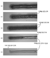
도 2는 레이저 펄스가 좌측으로부터 우측으로 연장하는 가공 궤적을 따라 전달되도록, 빔 축과 작업물(102) 사이의 상대적인 이동을 야기하는 동안 레이저 펄스가 전달되는, 본원에서 실리콘 웨이퍼로서 제공되는, 작업물(102)의 표면에 형성되는 트렌치 (a) 내지 (e)의 현미경 사진(평면도로 촬영됨)을 도시한다. 따라서, 각 트렌치의 선단은 현미경 사진의 좌측에 도시된 열에 나타나고, 트렌치 (a) 내지 (c)의 말단은 우측에 도시된 열에 나타난다. 트렌치 (d) 및 (e)의 말단의 외형은 트렌치 (c)의 말단의 외형과 실질적으로 동일하였다. 2 is a diagrammatic view of a
각 트렌치 (a) 내지 (e)는 35 μm의 스폿 크기, 800 fs의 펄스 지속기간, 및 6 μJ의 펄스 에너지를 갖는 레이저 펄스를 1855 kHz의 펄스 반복률로 빔 축을 따라 전파시킴으로써 형성되었다. 빔 축과 작업물(102) 사이의 상대적인 이동은 연속적으로 전달된 레이저 펄스가 트렌치 (a)에 대해 0.5 μm의 바이트 크기로, 트렌치 (b)에 대해 0.475 μm의 바이트 크기로, 트렌치 (c)에 대해 0.5 μm의 바이트 크기로, 트렌치 (d)에 대해 0.425 μm의 바이트 크기로, 및 트렌치 (e)에 대해 0.4 μm의 바이트 크기로, 작업물(102)에 충돌하도록 수행되었다. 트렌치 (a) 내지 (e)는 전달된 레이저 펄스를 가공 궤적을 따라 단일 패스로 스캔함으로써 형성되었다.Each of the trenches (a) through (e) was formed by propagating a laser pulse having a spot size of 35 μm, a pulse duration of 800 fs, and a pulse energy of 6 μJ at a pulse repetition rate of 1855 kHz along the beam axis. The relative movement between the beam axis and the
도 2에 도시된 바와 같이, 트렌치 (a)를 형성하도록 선택된 파라미터는 상당히 주목할 만한(noticeable) 잔해를 트렌치의 내부 및 외부 양자에 형성하였고, 거칠게 가공된 작업물 표면뿐만 아니라, 트렌치 엣지를 따라 가공된 면적 외부에 거친 작업물 표면을 초래하였다. 바이트 크기를 0.5 μm로부터 0.475 μm로 감소시킬 때, 트렌치 형성 가공은 트렌치 (b)의 길이 중 대부분을 따라 잔해를 생성하고, 다만 트렌치 (b)의 단부 또는 그 근처에는 잔해가 검출되지 않음이 관찰된다. 트렌치 (b)의 형성이 시작된 후, 어느 주목할 만한 잔해의 발생이 중단될 때까지 약 850 μs가 경과한 것으로 추정된다(즉, 잔해 트랜지션(transition) 주기는 약 850 μs이었다). 트렌치 (c), (d) 및 (e)의 형성 동안 바이트 크기를 각각 0.45 μm, 0.425 μm, 0.4 μm로 더 감소시킬 때, 잔해 트랜지션 주기는 각각 약 600 μs, 약 320 μs 및 약 305 μs로 감소된다. As shown in Fig. 2, the parameters selected to form the trench a have formed noticeable debris both on the interior and exterior of the trench, as well as on the rough machined workpiece surface, along the trench edge Resulting in a rough work surface outside the area. When reducing the byte size from 0.5 μm to 0.475 μm, the trench forming process creates debris along most of the length of the trench (b), but no debris is detected at or near the end of the trench (b) do. After the formation of the trench (b) has begun, it is estimated that approximately 850 μs have elapsed (ie, the transition period of the debris transition is approximately 850 μs) until the occurrence of any notable debris is discontinued. When further reducing the byte size to 0.45 μm, 0.425 μm, and 0.4 μm, respectively, during the formation of trenches (c), (d) and (e), the debris transition periods are about 600 μs, about 320 μs and about 305 μs, respectively .
어느 특정 이론으로 제한되는 것을 바라지 않으면서, 본 발명자는 레이저 펄스가 연속적으로 전달되는 작업물 내의 공간적 영역이 감소하기 때문에, 바이트 크기의 감소와 함께(스폿 크기, 펄스 지속기간, 펄스 에너지 및 펄스 반복률을 일정하게 유지하면서) 잔해 트랜지션 주기가 감소하는 것으로 간주한다. 이는 조사된 가공 스폿을 로컬로 둘러싸는 작업물(102) 내의 영역이 열을 누적하게 한다. 잔해 트랜지션 주기가 경과한 후에, 이들 영역(즉, 가공 궤적을 따라 위치된 영역) 중 일부의 온도는 상승된 상태로(즉, 제거될 재료의 기화 온도와 융해 온도 사이로) 유지된다. 작업물(102)의 이들 영역 내에 남아있는 잔여 열은 어느 주목할 만한 잔해를 생성하지 않으면서, 그 안의 재료의 효율적인 삭마를 가능케 한다.Without wishing to be bound by any particular theory, the inventors have found that, with a reduction in the size of the bite (spot size, pulse duration, pulse energy and pulse repetition rate Is maintained constant), the debris transition period is considered to be reduced. This causes the areas in the
B. 펄스 에너지와 잔해 발생 사이의 관계B. Relationship between pulse energy and debris generation
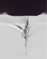
도 3은 좌측으로부터 우측으로 연장하는 가공 궤적을 따라 레이저 펄스가 전달되도록, 빔 축과 작업물(102) 사이의 상대적인 이동을 야기하는 동안 레이저 펄스가 전달되는, 본원에서 실리콘 웨이퍼로서 제공되는 작업물(102)의 표면 내에 형성된 트렌치 (a) 내지 (e)의 현미경 사진(평면도로 촬영됨)을 도시한다. 각 트렌치의 선단만이 도시된다.3 shows a
각 트렌치 (a) 내지 (e)는 35 μm의 스폿 크기, 800 fs의 펄스 지속기간을 갖는 레이저 펄스를 1979 kHz의 펄스 반복률로 빔 축을 따라 전파시킴으로써 형성되었다. 빔 축과 작업물(102) 사이의 상대적인 이동은 연속적으로 전달된 레이저 펄스가 각 트렌치에 대해 0.5 μm의 바이트 크기에서 작업물(102)에 충돌하도록 수행되었다. 작업물(102)로 전달된 레이저 펄스는 트렌치 (a)의 형성 동안 6 μJ의 펄스 에너지, 트렌치 (b)에 대해 5 μJ의 펄스 에너지, 트렌치 (c)에 대해 4 μJ의 펄스 에너지, 트렌치 (d)에 대해 3 μJ의 펄스 에너지 및 트렌치 (e)에 대해 2 μJ의 펄스 에너지를 구비하였다. 트렌치 (a)-(e)는 전달된 레이저 펄스를 가공 궤적을 따라 단일 패스로 스캔함으로써 형성된다. Each of the trenches (a) to (e) was formed by propagating a laser pulse having a spot size of 35 μm and a pulse duration of 800 fs at a pulse repetition rate of 1979 kHz along the beam axis. Relative movement between the beam axis and the
도 3에 도시된 바와 같이, 트렌치 (a)로부터 선택된 파라미터는 상당히 주목할 만한 잔해를 트렌치 외부의 선단 근처에 형성하였고, 가공된 면적 외부에 (선단으로부터 더 멀리 떨어진 트렌치를 따라 덜 주목할 만한) 거친 작업물 표면이지만 트렌치 내에서 상대적으로 매끄럽게 가공된 작업물 표면을 초래하였다. 펄스 에너지를 6 μJ로부터 5 μJ로 감소시킬 때, 트렌치 형성 가공은 트렌치 외부의 선단 근처에 상당히 주목할 만한 잔해(그리고, 선단으로부터 멀리 떨어진 트렌치를 따라 주목할 만한 잔해)를 발생시키며, 가공된 면적 외부의 거친 작업물 표면을 초래한다. 트렌치 (b) 내의 가공된 작업물 표면은 트렌치 (a) 내의 가공된 작업물 표면 보다 덜 매끄러운 것으로 관찰되었다. 펄스 에너지를 4 μJ로 더 감소시킬 때, 트렌치 형성 가공은 트렌치 (c)의 선단에 상당히 주목할 만한 잔해를 발생시키고, 가공된 면적 외부의 거친 작업물 표면을 뿐만 아니라, 트렌치 (c) 내에 거칠게 가공된 작업물 표면을 초래한다. 잔해는 또한, 트렌치 (a) 내지 (c)의 세로 방향(longitudinal) 면을 따라, 선단으로부터 말단까지 재구성 재료(recast material)의 릿지(ridge)의 형태로 있다. 펄스 에너지를 3 μJ로 더 감소시킬 때, 트렌치 형성 가공이 트렌치 (d)의 선단에 및 그 주위에 주목할 만한 잔해를 발생시키며, 가공된 면적 외부에 거친 작업물 표면뿐만 아니라, 트렌치 (d) 내에 거친 작업물 표면을 초래한다; 하지만, 상대적으로 짧은 잔해 트랜지션 주기 이후에, 주목할만한 잔해 발생은 관찰되지 않았다. 재구성 재료의 릿지는 또한, 트렌치 (d)의 선단으로부터 거리가 증가함에 따라 사라졌다. 2 μJ로 펄스 에너지를 더 감소시킬 때, 트렌치 형성 가공은 트렌치 (e)의 선단에서 또는 그 근처에서 트렌치 (e) 외부에 매우 적은 양의 잔해를 발생시키고, 트렌치 내에는 주목할 만한 잔해를 발생시키지 않는다. 하지만, 트렌치 (e) 내의 가공된 작업물 표면은 상당한 잔해가 관찰되지 않고, 매끄럽게 나타났다. 트렌치 (e) 외부에서 재구성 재료의 릿지는 관찰되지 않았다.As shown in Fig. 3, the parameter selected from the trench (a) has formed considerable debris near the tip of the exterior of the trench and has been subjected to a rough operation (less noticeable along the trench further away from the tip) Water surface but resulted in a relatively smoothly machined work surface within the trench. When the pulse energy is reduced from 6 [mu] J to 5 [mu] J, the trench formation process generates considerable debris (and noteworthy debris along the trench away from the tip) near the tip of the exterior of the trench, Resulting in a rough work surface. The machined workpiece surface in the trench (b) was observed to be less smooth than the machined workpiece surface in the trench (a). When further reducing the pulse energy to 4 [mu] J, the trench forming process generates considerable debris at the tip of the trench (c), and not only the rough work surface outside the machined area, but also rough machining Resulting in the surface of the workpiece. The debris is also in the form of a ridge of recast material from the tip to the end, along the longitudinal sides of the trenches (a) to (c). When the pulse energy is further reduced to 3 μJ, the trench forming process generates noticeable debris at and around the tip of the trench (d), leaving not only the rough work surface outside the machined area, but also within the trench (d) Resulting in a rough work surface; However, after a relatively short debris transition period, no noticeable debris was observed. The ridge of the reconstruction material also disappeared as the distance from the tip of the trench (d) increased. When further decreasing the pulse energy by 2 [mu] J, the trench forming process produces very little debris outside the trench (e) at or near the tip of the trench (e), causing significant debris within the trench Do not. However, the surface of the worked workpiece in the trench (e) did not show significant debris and appeared smooth. No ridges of the reconstituting material were observed outside of the trench (e).
C. 잔해 발생에서 크기 조정(Scaling)의 결과C. Scaling results from debris generation
도 4는 각각 본원에서 실리콘 웨이퍼로 제공된 작업물(102)의 표면에 형성된 교차하는 스크라이브 라인의 세트를 포함하는, 레이저 가공된 피처 (a) 및 (b)의 현미경 사진(평면도로 촬영됨)을 도시한다.4 shows a micrograph (taken in a plan view) of the laser-processed features (a) and (b), each containing a set of intersecting scribe lines formed on the surface of a
피처 (a) 및 (b)를 형성하기 위하여, 레이저 펄스가 각 스크라이브 라인에 대해 세 개의 평행한 스캔 라인을 포함하는 가공 궤적을 따라 전달되고, 각 스캔 라인이 단일 패스에서 다루어지도록, 빔 축과 작업물(102) 사이의 상대적인 이동을 야기하는 동안 레이저 펄스가 작업물(102)에 전달되었다. 각 피처 (a) 및 (b)는 800 fs의 펄스 지속기간을 갖는 레이저 펄스를 1855 kHz의 펄스 반복률로 빔 축을 따라 전파시킴으로써 형성되었다. 피처 (a)의 형성 동안 작업물(102)로 전달된 레이저 펄스는 25 μm의 스폿 크기와 3.14 μJ의 펄스 에너지를 가졌고, 빔 축과 작업물(102) 사이의 상대적인 이동은 연속적으로 전달된 레이저 펄스가 0.1 μm의 바이트 크기로 작업물(102)에 충돌하도록 수행되었다. 피처 (b)의 형성 동안 작업물(102)로 전달된 레이저 펄스는 35 μm의 스폿 크기와 6.16 μJ의 펄스 에너지를 가졌고, 빔 축과 작업물(102) 사이의 상대적인 이동은 연속적으로 전달된 레이저 펄스가 0.25 μm의 바이트 크기로 작업물(102)에 충돌하도록 수행되었다. To form features (a) and (b), a laser pulse is transmitted along a processing locus including three parallel scan lines for each scribe line, and each scan line is processed in a single pass, A laser pulse was delivered to the
도 4로부터 명백한 바와 같이, 피처 (a)의 형성 동안 상당한 양의 잔해가 발생되고, 눈에 보이는 피트(pit) 및 다른 손상을 갖는 거칠게 가공된 작업물 표면을 갖는 스크라이브 라인을 초래한다. 대조적으로, 피처 (b)의 형성 동안 잔해가 실질적으로 발생하지 않았으며, 생성된 스크라이브 라인은 실질적으로 누적된 잔해가 없는 매끄럽게 가공된 작업물 표면을 나타냈다. 주석: 점선 타원에 의해 둘러싸인 피처 (b)의 영역 내에는 상당한 잔해가 발생되었고 누적되었다. 이 영역은 두 번 가공된 피처의 영역에 대응한다. As is apparent from Fig. 4, a significant amount of debris is generated during formation of the feature (a), resulting in a scribe line having a roughened work surface with visible pits and other damage. In contrast, no debris was substantially generated during formation of feature (b), and the resulting scribe line exhibited a smoothly finished work surface with substantially no accumulated debris. NOTE: Significant debris has been generated and accumulated within the area of feature (b) surrounded by dotted ellipses. This area corresponds to the area of the twice machined feature.
D. 바이트 크기, 플루엔스 및 펄스 반복률과, 표면 거칠기 및 재료 제거 속도의 관계D. Relationship between byte size, fluence and pulse repetition rate, surface roughness and material removal rate
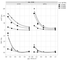
도 5는 전달된 레이저 펄스를 가공 궤적을 따라 단일 패스로 스캔하는 동안, 레이저 펄스를 빔 축을 따라 두 개의 펄스 반복률(즉, ~927 kHz 및 ~1855 kHz) 중 하나로 전파시킴으로써 본원에서 실리콘 웨이퍼로서 제공된 작업물(102)에 형성된 트렌치 내의 가공된 작업물 표면의 평균 표면 거칠기(Ra)와, 트렌치 형성 가공 동안 재료 제거 속도(um2-면적(Area)) 사이의 관계를, (μm로 측정된) 바이트 크기 및 (J/cm2로 측정된) 플루엔스의 함수로 도시하는 그래프의 세트이다. 평균 표면 거칠기(Ra)는 대상체를 50배로 확대하는 Keyence 3D 공초점 현미경(confocal microscope)을 사용하여 측정되었다. 5 is a graphical representation of a laser pulse delivered here as a silicon wafer by propagating the laser pulse along one of two pulse repetition rates (i.e., ~ 927 kHz and ~ 1855 kHz) along the beam axis, while scanning the transferred laser pulse in a single pass along the processing locus. The relationship between the average surface roughness (Ra) of the machined workpiece surface in the trench formed in the
도 5로부터 명백해지는 바와 같이, 가공된 작업물 표면의 평균 표면 거칠기는 0.2 μm를 초과하는 바이트 크기에서, 약 0.25 μm 아래로 떨어지며, 미러처럼 매끄러운 표면 마감(mirror-smooth surface finish)에 도달한다. ~1855 kHz의 펄스 반복률로 전달된 레이저 펄스를 사용하여 형성된 가공된 작업물 표면의 평균 표면 거칠기는, 시험된 모든 바이트 크기 및 플루엔스 수준에 대해, ~927 kHz의 펄스 반복률로 전달된 레이저 펄스를 사용하여 형성된 대응하는 가공된 작업물 표면보다 일반적으로 낮다. um2-면적 값은 스크라이브의 횡단 면적을 나타내고, 바이트 크기가 증가함에 따라 재료 제거 속도가 감소함을 나타낸다. ~927 kHz의 펄스 반복률에서 트렌치의 형성 동안 획득된 재료 제거 속도는 ~1855 kHz의 펄스 반복률에서 트렌치의 형성 동안 획득된 재료 제거 속도와 유사하다. As can be seen from Figure 5, the average surface roughness of the machined workpiece surface falls below about 0.25 占 퐉 at a bite size exceeding 0.2 占 퐉 and reaches a mirror-smooth surface finish like a mirror. The average surface roughness of the machined workpiece surface formed using laser pulses delivered at a pulse repetition rate of ~ 1855 kHz was calculated using a laser pulse delivered at a pulse repetition rate of ~ 927 kHz for all byte sizes and fluence levels tested Is generally lower than the corresponding machined work surface formed using. The um2-area value represents the cross-sectional area of the scribe, indicating that the material removal rate decreases as the byte size increases. The material removal rate obtained during the formation of the trench at a pulse repetition rate of ~ 927 kHz is similar to the material removal rate obtained during formation of the trench at a pulse repetition rate of ~ 1855 kHz.
E. 바이트 크기, 플루엔스, 펄스 반복률 및 평균 전력과 잔해 발생의 관계E. Relationship between byte size, fluence, pulse repetition rate and average power and debris generation
도 6은 i) 주목할만하게 발생한 잔해 없이, 가공된 작업물 표면의 형성을 초래하고(즉, 도 2 내지 도 5에 대하여 논의된 바와 같이, 그 위에 주목할 만하게 누적된 잔해가 없는 가공된 작업물 표면을 초래하고), ii) 주목할 만하게 발생한 잔해를 갖는 가공된 작업물 표면의 형성을 초래하는(즉, 도 2 내지 도 5에 대해 논의된 바와 같이, 그 위에 주목할 만한 잔해가 누적된 가공된 작업물 표면을 초래하는), 본원에서 실리콘 웨이퍼로서 제공된 작업물(102)에서 트렌치를 형성하는 가공 윈도우를 도시하는 그래프의 세트를 도시한다. 참조 부호(600)로 표시된 패턴으로 구분된 영역은 주목할만한 잔해의 발생을 초래하는 파라미터 공간을 나타내고, 참조 부호(602)로 표시된 패턴으로 구분된 영역은 주목할 만한 잔해의 발생을 초래하지 않는 파라미터 공간을 나타낸다. 관찰된 트렌치는 전달된 레이저 펄스를 가공 궤적을 따라 단일 패스로 스캔하는 동안, 레이저 펄스를 다섯 개의 펄스 반복률 (i.e., 927.55 kHz, 1264 kHz, 1855 kHz, 2022 kHz 및 3051 kHz) 중 하나로 빔 축을 따라 전파시킴으로써 형성되었다. 각 펄스 반복률에서, 다수의 트렌치가 형성되었고, 각 트렌치는 (μm로 측정된) 바이트 크기, (J/cm2로 측정된) 플루엔스 및 (W로 측정된) 평균 전력의 상이한 조합을 사용하여 형성되었다.Fig. 6 is a schematic diagram of a process for the production of a finished workpiece surface that results in the formation of a machined workpiece surface (i. E., As discussed with respect to Figs. 2-5) (I. E., Resulting in the formation of a machined work surface having noteworthy debris) (i. E., As discussed with respect to Figures 2 to 5, (Which results in the surface of the workpiece 102), a processing window that forms a trench in a
도 6에 도시된 바와 같이, 927.55 kHz 및 1264 kHz에서, 시험된 바이트 크기, 플루엔스 및 평균 전력 값의 모든 조합은 적당한 내지 상당한 양의 잔해를 발생시키는 것으로 관찰된 한편, 1855 kHz, 2022 kHz 및 3051 kHz에서 파라미터 값의 일부(전체가 아님) 조합은 적은 잔해 내지 누적된 잔해가 없는 가공된 작업물 표면을 생성하는 것으로 확인되었다. 이 결과는 가공될 특정 재료에 대해, 그 밑으로는 잔해 발생이 회피될 수 없는 임계 펄스 반복률이 존재함을 나타낸다. 하지만, 임계 펄스 반복률을 초과하여, 일부 다른 일반적인 관찰이 이루어질 수 있다: 상대적으로 낮은 플루엔스 또는 평균 전력 값에서, 적당하거나 상당한 양의 잔해를 발생시키지 않으면서 피처를 형성하도록 상대적으로 넓은 범위의 바이트 크기를 사용하여 작업물(102)이 가공될 수 있다; 그리고, 플루엔스 또는 평균 전력이 증가할 때 이 범위의 바이트 크기는 감소한다. As shown in Figure 6, at 927.55 kHz and 1264 kHz, all combinations of tested byte size, fluence, and average power values were observed to produce modest to significant amounts of debris, while 1855 kHz, 2022 kHz and At 3051 kHz, some (but not all) combinations of parameter values were found to produce a machined work surface with little debris or accumulated debris. This result indicates that for a particular material to be processed there is a critical pulse repetition rate beneath which debris generation can not be avoided. However, beyond the critical pulse repetition rate, some other general observations can be made: at a relatively low fluence or average power value, a relatively wide range of bytes to form a feature without generating a modest or significant amount of debris The
영역(600 및 602)이 중첩되는 일부 파라미터 공간이 있다. 예를 들어, 참조 부호(604)로 표시된 패턴에 의해 구분된 영역을 참조한다. 이 중첩은 (1) 상당하거나 주목할만한 잔해 발생과 상당하지 않거나 주목할 만하지 않은 잔해 발생 사이의 트랜지션이 있거나; 또는 (2) 주어진 플루엔스, 전력 및 바이트 크기에 대해, 깨끗하고 매끄러운 피처 또는 잔해 발생에 의해 동반될 수 있는 피처를 생성할 수 있는 가공이 있음을 나타내는 것으로 일반적으로 이해될 수 있다. 1855 kHz에서의 예시로서, 전력 및 플루엔스에 매칭하는 공정에 대하여, 상이한 결과(즉, 깨끗하고 매끄러운 피처 또는 잔해의 발생이 동반되는 피처)를 생성하는 스폿 크기 및 펄스 에너지의 조합이 있다. 달리 말하자면, 영역(600 및 602)이 중첩되는 파라미터 공간 내의 주어진 좌표에서, 깨끗하고 매끄러운 표면을 갖는 피처 또는 잔해의 발생이 동반되는 피처는 전달된 레이저 펄스의 스폿 크기 및 펄스 에너지에 의존하여 형성될 수 있다. There are some parameter spaces where
IV. 실험 결과에 기반한 예시적인 실시예IV. An exemplary embodiment based on experimental results
섹션 III, 하위 섹션 A 내지 E에서 상술한 실험의 결과를 기초로, 본 발명의 일 실시예는 제거 가공 동안, (작업물(102)로 전달된 레이저 펄스에서 광의 파장에 대해 투명하지 않은) 재료를 제거함으로써, 작업물(102)에 피처(예를 들어, 스크라이브 또는 다른 트렌치 또는 리세스 등)를 형성하는 레이저 가공으로 특징지어질 수 있다. 예를 들어, 그리고 도 9a에 도시된 실시예를 참조하면, 작업물(102)은 상부 표면(예를 들어, 표면(900a)) 및 상부 표면 반대편의 하부 표면(예를 들어, 표면(900b))을 갖는 반도체 웨이퍼로서 제공될 수 있다. 반도체 웨이퍼는 (예를 들어, 실리콘, 게르마늄, Si1-xGex(여기서, 0.0001 < x < 0.9999), GaAs, GaN, InP 등 또는 이들의 어느 조합과 같은 재료로 형성되는) 기판(902), 및 (예를 들어, 하나 이상의 전계 효과 트랜지스터, 유전체 층, 상호 연결 금속 배선 구조(interconnect metallization structures), 패시베이션 층(passivation layers) 등 또는 이들의 어느 조합으로 형성된) 디바이스 층(904)을 포함할 수 있다. 작업물(102)은 위에서 논의한 반도체 웨이퍼와는 다른 어느 방식으로 제공될 수 있음이 인식되어야 한다. 예를 들어, 작업물(102)은 (예를 들어, Al2O3, AlN, BeO, Cu, GaAs, GaN, Ge, InP, Si, SiO2, SiC, Si1-xGex (여기서 0.0001 < x < 0.9999) 등 또는 이들의 어느 조합 또는 합금으로 형성된 기판(예를 들어, 전자 기판, 반도체 기판, 광학 기판 등), 플라스틱, 유리(예를 들어, 열적으로, 화학적으로, 또는 다른 방식으로 강화되거나 강화되지 않음), 석영, 사파이어, 플라스틱, 실리콘 등으로 형성된 물품, 하나 이상의 금속(예를 들어, Al, Ag, Au, Cu, Fe, In, Mg, Pt, Sn, Ti 등, 또는 이들의 조합 또는 합금), 전도성 금속 산화물(예를 들어, ITO 등), 투명한 전도성 폴리머, 세라믹, 왁스, 수지, (예를 들어, 산화규소, 질화규소, 산질화규소 등 또는 이들의 어느 조합과 같은 중간층 유전체 구조로 사용되는) 무기 유전 재료, 로우-k 유전 재료(예를 들어, 메틸 실세스퀴옥산(MSQ), 하이드로겐 실세스퀴옥산(HSQ), 플루오르화 테트라에틸 오소실리케이트(FTEOS) 등 또는 이들의 어느 조합), 유기 유전 재료(예를 들어, (모두 도우 사에서 제조된) SILK, 벤조시클로부텐, 노틸러스, (듀퐁 사에서 제조된) 폴리플루오로테트라에틸렌, (얼라이드 케미컬 사에서 제조된) FLARE 등 또는 이들의 어느 조합), 유리 섬유, 폴리머 재료(폴리아미드, 폴리이미드, 폴리에스테르, 폴리아세탈, 폴리카보네이트, 변성 폴리페닐렌 에테르, 폴리부틸렌 테레프탈레이트, 폴리페닐렌 설파이드, 폴리에테르 술폰, 폴리에테르 이미드, 폴리에테르 에테르 케톤, 액정 폴리머, 아크릴로니트릴 부타디엔 스티렌 및 이들의 어느 화합물, 조성물 또는 합금) 등 또는 이들의 어느 조합을 포함하는 어느 단일 또는 다중 층 구조로 제공될 수 있다.Based on the results of the experiments described above in Section III, subsections A through E, one embodiment of the present invention provides a method for removing material (not transparent to the wavelength of light in the laser pulse delivered to the workpiece 102) (E.g., scribe or other trenches or recesses) in the
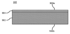
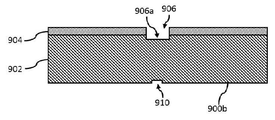
작업물(102)의 일부가 다음: 가공 동안 잔해의 최소 발생 또는 발생 없음; 매끄럽게 가공된 작업물 표면의 생성; 감소된 수의 결함, 흠(flaws) 또는 균열을 갖는 가공된 작업물 표면의 생성; 가공된 작업물 표면에 인접한 작업물(102)의 균일한 HAZ의 생성 중 하나 이상을 이롭게 달성하는 방식으로 제거됨을 보장하기 위하여, 제거 가공의 파라미터들(예를 들어, 플루엔스, 평균 전력, 펄스 반복률, 펄스 에너지, 스폿 크기, 바이트 크기 등 중 하나 이상)이 선택되거나, 제어되거나, 또는 다른 방식으로 설정된다. 예를 들어, 제거 가공 동안, 작업물(102)의 상부 표면(900a)에 피처(예를 들어, 리세스, 트렌치 등일 수 있는, 도 9b에 도시된 피처(906))를 형성하기 위해, 레이저 펄스 빔은 작업물(102)과 교차하는 빔 축을 따라 지향될 수 있고, 레이저 펄스 빔은 연속적으로 지향된 레이저 펄스가 0이 아닌 바이트 크기로 작업물(102) 위에 충돌하도록 스캔될 수 있다.Part of the
도 9b에 도시된 실시예에서, 피처(906)는 디바이스 층(904)을 통해 완전히, 그리고 기판(902)내로 부분적으로 (예를 들어, 기판(902)의 상부 표면으로부터 측정된 깊이 (d) 만큼) 연장한다. 일부 실시예에서, 깊이(d)는 5 μm(또는 그 즈음) 내지 22 μm(또는 그 즈음)의 범위 내에 있을 수 있다. 예를 들어, 깊이(d)는 5 μm, 5.5 μm, 6.0 μm, 6.5 μm, 7.0 μm, 7.5 μm, 8.0 μm, 8.5 μm, 10 μm, 12 μm, 15 μm, 17 μm, 20 μm, 22 μm 등, 또는 이들 값 중 어느 것 사이일 수 있다. 그렇지만, 깊이(d)가 5 μm 미만이거나, 22 μm를 초과할 수 있음이 인식되어야 한다. 다른 실시예에서, 피처(906).9B, the
파라미터가 충분히 매끄러운 가공된 작업물 표면(예를 들어, 가공된 작업물 표면(906))을 생성하도록 선택된 경우, 가공된 작업물 표면은 작업물(102)의 초기 가공, 작업물(102)의 관통 작업물 가공 등 또는 이들의 어느 조합과 같은 후속 가공을 용이하게 하도록 사용될 수 있다. 가공된 작업물 표면(예를 들어, 가공된 작업물 표면(906))은 가공된 작업물 표면이 1.0 μm 이하의 평균 표면 거칠기(Ra)를 갖는 경우 후속 가공을 용이하게 하도록 "충분히 매끄러운" 것으로 간주될 수 있다. 일부 실시예에서, 가공된 작업물 표면은 1.0 μm 미만, 0.75 μm 미만, 0.5 μm 미만, 0.4 μm 미만, 0.3 μm 미만, 0.25 μm 미만, 0.2 μm 미만, 0.15 μm 미만 등 또는 이들 값 중 어느 것 사이의 평균 표면 거칠기(Ra)를 갖는다.If the parameter is selected to produce a sufficiently smooth machined workpiece surface (e.g., a machined workpiece surface 906), then the machined workpiece surface can be used for initial machining of the
작업물(102)의 내부 가공은 처음에 가공된 작업물 표면을 통해, 그 후 작업물로 통과하도록 다른 레이저 펄스 빔을 지향시킴으로써 수행될 수 있다. 이 경우, 지향된 레이저 펄스 빔은 레이저 펄스의 빔 웨이스트가 작업물(102) 내부에 위치되도록 집속된다. 작업물(102)의 내부 가공 동안 사용되는 레이저 펄스는 가공된 작업물 표면의 초기 형성 동안 사용되는 파장보다, 가공되고 있는 작업물(102) 내의 재료에 대해 더욱 투명한 파장을 갖는다. 이러한 내부 가공과 연관된 파라미터(예를 들어, 플루엔스, 평균 전력, 펄스 반복률, 펄스 에너지, 스폿 크기, 바이트 크기 등 중 하나 이상)는 작업물(102) 내의 재료에 의해 지향된 레이저 펄스의 비선형 흡수를 유도하여, 그를 통해 전달된 레이저 펄스의 빔 웨이스트에 또는 그 근처에 있는 작업물(102) 내의 재료 중 일 부분(예를 들어, 도 9c에 도시된 부분(908))을 가공하도록 (예를 들어, 융해, 기화, 삭마, 균열, 변색 등을 하도록, 또는 화학적 조성, 결정 구조, 전자 구조, 미세 구조, 나노 구조, 밀도, 속도, 굴절률, 투자율, 유전 상수 등과 같은 하나 이상의 특성 또는 특징을 다른 방식으로 변경하도록) 선택된다. 예를 들어, 실리콘 웨이퍼와 같은 작업물(102)에 트렌치가 형성된 후에, 충분히 매끄럽게 가공된 작업물 표면(예를 들어, 도 7의 현미경 사진에 도시됨)을 생성하기 위해, 실리콘 웨이퍼 내부에 일련의 균열(예를 들어, 도 8a 및 도 8b의 현미경 사진에 도시됨 - 도 8a는 도 7에 도시된 트렌치의 폭을 가로지르는 도면을 도시하고, 도 8b는 도 7에 도시된 트렌치의 길이를 따른 도면을 도시함 -)을 형성하도록 상술한 내부 가공이 수행될 수 있다.Internal processing of the
도 9d를 참조하면, 작업물(102)의 관통 작업물 가공은 처음에 가공된 작업물 표면(예를 들어, 가공된 작업물 표면(906a))을 통해, 그 후 작업물로 통과하도록 다른 레이저 펄스 빔을 지향시킴으로써 수행될 수 있다. 지향된 레이저 펄스 빔은, 레이저 펄스의 빔 웨이스트가 작업물(102)의 하부 표면(900b)에 또는 그 근처에 위치되도록 집속된다. 작업물(102)의 내부 가공 동안 사용된 레이저 펄스는 가공된 작업물 표면의 초기 형성 동안 사용되는 파장 보다, 가공되고 있는 작업물(102) 내의 재료에 대해 더욱 투명한 파장을 갖는다. 이러한 관통 작업물 가공과 연관된 파라미터(예를 들어, 플루엔스, 평균 전력, 펄스 반복률, 펄스 에너지, 스폿 크기, 바이트 크기 등 중 하나 이상)는 하부 표면(900b)에서 작업물(102)의 재료에 의해 지향된 레이저 펄스의 선형 또는 비선형 흡수를 야기하여, 전달된 레이저 펄스의 빔 웨이스트에 또는 그 근처에 있는 작업물(102) 중 일부를 가공하도록(예를 들어, 하부 표면(900b)에 트렌치 또는 리세스(910)를 형성하도록) 선택된다. 수행될 수 있는 작업물(102)의 관통 작업물 가공의 일부 예시는 그 전체가 본원에 참조로 통합되는, 미국특허번호 제9,610,653호에 서술된다.9D, penetrating workpiece processing of
V. 결론V. Conclusion
전술한 것은 본 발명의 실시예 및 예시를 예시하는 것일 뿐, 본 발명을 제한하는 것으로 해석되어서는 안 된다. 수개의 특정한 실시예 및 예시가 도면을 참조로 서술되었지만, 이 분야의 기술자는 본 발명의 새로운 교시와 장점을 실질적으로 벗어나지 않으면서, 개시된 실시예 및 예시는 물론 다른 실시예에 대한 다수의 변형이 가능함을 쉽게 인식할 것이다. The foregoing is merely illustrative of the embodiments and examples of the invention, and should not be construed as limiting the invention. Although a few specific embodiments and examples have been described with reference to the drawings, those skilled in the art will appreciate that many variations of the disclosed embodiments and examples, as well as other embodiments, may be made without departing substantially from the novel teachings and advantages of the present invention It is easy to recognize that it is possible.
예를 들어, 위의 섹션 III에서 논의된 실험이 그저 실리콘 웨이퍼 상에서만 수행되었더라도, 가공될 재료가 전달된 레이저 펄스의 파장에 대해 투명하지 않는 한, 초단 레이저 펄스를 사용하여 (실리콘 웨이퍼 이외의) 재료를 포함하는 작업물을 가공할 때 유사한 결과가 관찰될 수 있음이 인식되어야 한다. 따라서, 전술한 실시예는 실리콘, 전자 또는 광학 디바이스 기판(예를 들어, Al2O3, AlN, BeO, Cu, GaAs, GaN, Ge, InP, Si, SiO2, SiC, Si1-xGex (여기서 0.0001 < x < 0.9999) 등 또는 이들의 어느 조합 또는 합금으로 형성된 기판), 플라스틱, 유리(예를 들어, 열적으로, 화학적으로, 또는 다른 방식으로 강화되거나 강화되지 않음), 석영, 사파이어, 플라스틱, 실리콘 등으로 형성된 물품, 하나 이상의 금속(예를 들어, Al, Ag, Au, Cu, Fe, In, Mg, Pt, Sn, Ti 등, 또는 이들의 조합 또는 합금), 전도성 금속 산화물(예를 들어, ITO 등), 투명한 전도성 폴리머, 세라믹, 왁스, 수지, (예를 들어, 산화규소, 질화규소, 산질화규소 등 또는 이들의 어느 조합과 같은 중간층 유전체 구조로 사용되는) 무기 유전 재료, 로우-k 유전 재료(예를 들어, 메틸 실세스퀴옥산(MSQ), 하이드로겐 실세스퀴옥산(HSQ), 플루오르화 테트라에틸 오소실리케이트(FTEOS) 등 또는 이들의 어느 조합), 유기 유전 재료(예를 들어, (모두 도우 사에서 제조된) SILK, 벤조시클로부텐, 노틸러스, (듀퐁 사에서 제조된) 폴리플루오로테트라에틸렌, (얼라이드 케미컬 사에서 제조된) FLARE 등 또는 이들의 어느 조합), 유리 섬유, 폴리머 재료(폴리아미드, 폴리이미드, 폴리에스테르, 폴리아세탈, 폴리카보네이트, 변성 폴리페닐렌 에테르, 폴리부틸렌 테레프탈레이트, 폴리페닐렌 설파이드, 폴리에테르 술폰, 폴리에테르 이미드, 폴리에테르 에테르 케톤, 액정 폴리머, 아크릴로니트릴 부타디엔 스티렌 및 이들의 어느 화합물, 조성물 또는 합금) 등 또는 이들의 어느 조합 이외의 재료로 형성된 반도체 웨이퍼를 가공하는데 이롭게 채택될 수 있음이 인식되어야 한다.For example, even if the experiment discussed in Section III above was performed only on silicon wafers, using ultra-short laser pulses (other than silicon wafers), as long as the material to be processed is not transparent to the wavelength of the transmitted laser pulses, It should be appreciated that similar results can be observed when processing a workpiece containing the material. Therefore, the above-described embodiment is silicon, electronic or optical device substrate (e.g., Al 2 O 3, AlN, BeO, Cu, GaAs, GaN, Ge, InP, Si, SiO 2, SiC, Si 1-x Ge x , where 0.0001 < x < 0.9999, etc., or any combination or alloy thereof), plastic, glass (e.g., thermally, chemically or otherwise not tempered or tempered), quartz, sapphire (For example, Al, Ag, Au, Cu, Fe, In, Mg, Pt, Sn, Ti, or a combination or alloy thereof), conductive metal oxides Inorganic dielectric materials such as ITO and the like), transparent conductive polymers, ceramics, waxes, resins, (e.g., used in interlayer dielectric structures such as silicon oxide, silicon nitride, oxynitride, -k dielectric material (e.g., methyl silsesquioxane (MSQ), hydrogen silsesquioxane (HSQ) , SILK (benzophenone), benzocyclobutene, Nautilus (manufactured by DuPont), poly (tetraethyl orthosilicate (FTEOS) or any combination thereof), organic dielectric materials Glass fibers, polymeric materials (such as polyamides, polyimides, polyesters, polyacetals, polycarbonates, modified polyphenylene ethers, poly (ethylene terephthalate), poly Butylene terephthalate, polyphenylene sulfide, polyether sulfone, polyether imide, polyether ether ketone, liquid crystal polymer, acrylonitrile butadiene styrene, and any compounds, compositions or alloys thereof), or any combination thereof. It should be appreciated that the present invention can be advantageously employed in processing a semiconductor wafer formed of a material.
따라서, 이러한 모든 변형은 청구항으로 한정된 본 발명의 범위 내에 포함되는 것으로 의도된다. 예를 들어, 기술자는 어느 문장, 단락, 예시 또는 실시예의 주제가 그 조합이 상호 배타적인 경우를 제외하고, 다른 문장, 단락, 예시 또는 실시예 중 일부 또는 전체의 주제와 조합될 수 있다는 점을 인식할 것이다. 그러므로, 본 발명의 범위는 다음의 청구범위에 의해 결정되어야 하고, 청구범위의 균등물도 그 안에 포함될 것이다.Accordingly, all such modifications are intended to be included within the scope of the present invention as defined by the claims. For example, a technician may recognize that the subject matter of any sentence, paragraph, example, or embodiment may be combined with any or all of the other sentences, paragraphs, illustrations, or examples, except where the combination is mutually exclusive something to do. Therefore, the scope of the present invention should be determined by the following claims, and equivalents of the claims will be included therein.
Claims (15)
500 kHz를 초과하는 펄스 반복률, 스폿 크기 및 펄스 에너지에서 200 ps 미만의 펄스 지속기간을 갖는 제1 레이저 펄스 빔을 생성하는 것; 및
상기 작업물에 교차하는 빔 축을 따라 상기 제1 레이저 펄스 빔을 지향시키는 것;
상기 작업물의 상기 제1 표면에 피처(feature)를 형성하기 위해 연속적으로 지향된 레이저 펄스가 0이 아닌 바이트 크기로 상기 작업물에 충돌하고, 1.0 μm 미만의 평균 표면 거칠기(Ra)를 갖는 가공된 작업물 표면을 갖는 것으로 상기 피처가 특징지어지도록, 가공 궤적을 따라 상기 빔 축을 스캔하는 것을 포함하는 방법.Providing a workpiece having a first surface and a second surface opposite the first surface;
Generating a first laser pulse beam having a pulse repetition rate greater than 500 kHz, a spot size, and a pulse duration less than 200 ps in pulse energy; And
Directing the first laser pulse beam along a beam axis intersecting the workpiece;
Characterized in that a successively directed laser pulse impinges on the workpiece at a non-zero byte size to form a feature on the first surface of the workpiece, wherein the processed laser pulse has a mean surface roughness (Ra) And scanning the beam axis along a processing locus such that the feature is characterized as having a workpiece surface.
제2 레이저 펄스 빔을 생성하는 것;
빔 웨이스트(beam waist)를 생성하기 위하여 상기 제2 레이저 펄스 빔 내에 레이저 펄스를 집속하는 것;
상기 빔 웨이스트가 상기 작업물 내에 또는 상기 작업물의 제2 표면에 배열되도록, 상기 집속된 제2 레이저 펄스 빔을 상기 가공된 작업물 표면과 교차하는 빔 축을 따라 지향시키는 것; 및
상기 빔 웨이스트에서 상기 작업물을 가공하는 것을 더 포함하는 방법.14. The method according to any one of claims 1 to 13,
Generating a second laser pulse beam;
Focusing laser pulses in the second laser pulse beam to produce a beam waist;
Directing the focused second laser pulse beam along a beam axis intersecting the machined workpiece surface such that the beam waist is arranged in the workpiece or on a second surface of the workpiece; And
And processing the workpiece in the beam waist.
Applications Claiming Priority (3)
| Application Number | Priority Date | Filing Date | Title |
|---|---|---|---|
| US201662368053P | 2016-07-28 | 2016-07-28 | |
| US62/368,053 | 2016-07-28 | ||
| PCT/US2017/043229 WO2018022441A1 (en) | 2016-07-28 | 2017-07-21 | Laser processing apparatus and methods of laser-processing workpieces |
Publications (1)
| Publication Number | Publication Date |
|---|---|
| KR20190025721A true KR20190025721A (en) | 2019-03-11 |
Family
ID=61016598
Family Applications (1)
| Application Number | Title | Priority Date | Filing Date |
|---|---|---|---|
| KR1020197004389A KR20190025721A (en) | 2016-07-28 | 2017-07-21 | Laser processing apparatus and method for laser processing a workpiece |
Country Status (6)
| Country | Link |
|---|---|
| EP (1) | EP3490750A4 (en) |
| JP (1) | JP2019532815A (en) |
| KR (1) | KR20190025721A (en) |
| CN (1) | CN109862991A (en) |
| TW (1) | TW201803674A (en) |
| WO (1) | WO2018022441A1 (en) |
Families Citing this family (6)
| Publication number | Priority date | Publication date | Assignee | Title |
|---|---|---|---|---|
| JP7366045B2 (en) * | 2018-03-22 | 2023-10-20 | アプライド マテリアルズ インコーポレイテッド | Laser polishing of ceramic surfaces of processed components used in the manufacture of semiconductor devices |
| JP7336465B2 (en) * | 2018-05-08 | 2023-08-31 | ラム リサーチ コーポレーション | Atomic Layer Etching and Atomic Layer Deposition Processing Systems Including Telecentric Lenses, Optical Beam Folding Assemblies, or Lens Circuits with Polygon Scanners |
| EP3774166A4 (en) * | 2018-06-05 | 2022-01-19 | Electro Scientific Industries, Inc. | Laser-processing apparatus, methods of operating the same, and methods of processing workpieces using the same |
| CN113412453A (en) * | 2019-02-19 | 2021-09-17 | Asml控股股份有限公司 | Laser rough machining: engineering roughness of burl tops |
| CN113977099B (en) * | 2021-12-07 | 2023-12-19 | 北京卫星制造厂有限公司 | Ultrafast laser milling method for fiber composite material |
| TWI826980B (en) * | 2022-03-25 | 2023-12-21 | 國立陽明交通大學 | Method for fabricating an liquid-crystal-aligning electrode and method for fabricating a liquid crystal cell using the same |
Family Cites Families (17)
| Publication number | Priority date | Publication date | Assignee | Title |
|---|---|---|---|---|
| CA2009514C (en) * | 1990-02-07 | 1995-04-25 | Mahmud U. Islam | Laser rough and finish machining of hard materials |
| JP2005116844A (en) * | 2003-10-09 | 2005-04-28 | Matsushita Electric Ind Co Ltd | Method for manufacturing semiconductor device |
| US20060000814A1 (en) * | 2004-06-30 | 2006-01-05 | Bo Gu | Laser-based method and system for processing targeted surface material and article produced thereby |
| US20060039419A1 (en) * | 2004-08-16 | 2006-02-23 | Tan Deshi | Method and apparatus for laser trimming of resistors using ultrafast laser pulse from ultrafast laser oscillator operating in picosecond and femtosecond pulse widths |
| JP2007021527A (en) * | 2005-07-15 | 2007-02-01 | Matsushita Electric Ind Co Ltd | Laser beam machining method |
| US9138913B2 (en) * | 2005-09-08 | 2015-09-22 | Imra America, Inc. | Transparent material processing with an ultrashort pulse laser |
| FI20060177L (en) * | 2006-02-23 | 2007-08-24 | Picodeon Ltd Oy | The method produces good quality surfaces and a product with a good quality surface |
| CN105583526B (en) * | 2008-03-21 | 2018-08-17 | Imra美国公司 | Material processing method based on laser and system |
| GB2459669A (en) * | 2008-04-30 | 2009-11-04 | Xsil Technology Ltd | Dielectric layer pulsed laser scribing and metal layer and semiconductor wafer dicing |
| US20110287217A1 (en) * | 2010-05-21 | 2011-11-24 | Prantik Mazumder | Superoleophobic substrates and methods of forming same |
| JP2012156168A (en) * | 2011-01-21 | 2012-08-16 | Disco Abrasive Syst Ltd | Division method |
| US8685599B1 (en) * | 2011-02-24 | 2014-04-01 | Sandia Corporation | Method of intrinsic marking |
| US10357850B2 (en) * | 2012-09-24 | 2019-07-23 | Electro Scientific Industries, Inc. | Method and apparatus for machining a workpiece |
| EP3077149A4 (en) * | 2013-12-05 | 2017-09-20 | Electro Scientific Industries, Inc. | Method and apparatus for internally marking a substrate having a rough surface |
| US9850160B2 (en) * | 2013-12-17 | 2017-12-26 | Corning Incorporated | Laser cutting of display glass compositions |
| CN105108343B (en) * | 2015-09-22 | 2017-08-22 | 武汉金顿激光科技有限公司 | A kind of process of surface treatment of container soldering joint |
| CN105468873B (en) * | 2015-12-24 | 2018-08-14 | 中北大学 | The surface-smoothing emulation mode of silicon substrate laser optical waveguide |
-
2017
- 2017-07-21 EP EP17835014.6A patent/EP3490750A4/en not_active Withdrawn
- 2017-07-21 CN CN201780054282.5A patent/CN109862991A/en not_active Withdrawn
- 2017-07-21 JP JP2019504698A patent/JP2019532815A/en active Pending
- 2017-07-21 KR KR1020197004389A patent/KR20190025721A/en not_active Application Discontinuation
- 2017-07-21 WO PCT/US2017/043229 patent/WO2018022441A1/en unknown
- 2017-07-27 TW TW106125299A patent/TW201803674A/en unknown
Also Published As
| Publication number | Publication date |
|---|---|
| TW201803674A (en) | 2018-02-01 |
| EP3490750A4 (en) | 2020-04-29 |
| JP2019532815A (en) | 2019-11-14 |
| EP3490750A1 (en) | 2019-06-05 |
| WO2018022441A1 (en) | 2018-02-01 |
| CN109862991A (en) | 2019-06-07 |
Similar Documents
| Publication | Publication Date | Title |
|---|---|---|
| US20210316400A1 (en) | Laser processing apparatus, methods of laser-processing workpieces and related arrangements | |
| KR20190025721A (en) | Laser processing apparatus and method for laser processing a workpiece | |
| Knowles et al. | Micro-machining of metals, ceramics and polymers using nanosecond lasers | |
| JP6220775B2 (en) | Laser direct ablation at high pulse repetition frequency using picosecond laser pulses | |
| JP5432285B2 (en) | Method of laser processing glass into a shape with chamfered edges | |
| US6676878B2 (en) | Laser segmented cutting | |
| JP7146770B2 (en) | Method and system for extending the life of optical components in laser processing equipment | |
| TWI647187B (en) | Method of separating a glass sheet from a carrier | |
| JP2010536576A (en) | Solid material cutting method and system using short pulse laser | |
| US20210331273A1 (en) | Laser processing apparatus and methods of laser-processing workpieces | |
| Karnakis et al. | High power DPSS laser micromachining of silicon and stainless steel | |
| Bovatsek et al. | Ultrashort pulse micromachining with the 10-μJ FCPA fiber laser | |
| KR20030077598A (en) | Ultraviolet laser ablative patterning of microstructures in semiconductors | |
| Vanttaja et al. | Laser applications in electronics industry |
Legal Events
| Date | Code | Title | Description |
|---|---|---|---|
| E902 | Notification of reason for refusal | ||
| E601 | Decision to refuse application |