KR20180098626A - Imprint apparatus and method of manufacturing article - Google Patents
Imprint apparatus and method of manufacturing article Download PDFInfo
- Publication number
- KR20180098626A KR20180098626A KR1020187021645A KR20187021645A KR20180098626A KR 20180098626 A KR20180098626 A KR 20180098626A KR 1020187021645 A KR1020187021645 A KR 1020187021645A KR 20187021645 A KR20187021645 A KR 20187021645A KR 20180098626 A KR20180098626 A KR 20180098626A
- Authority
- KR
- South Korea
- Prior art keywords
- substrate
- mold
- imprint
- gas
- stage
- Prior art date
- Legal status (The legal status is an assumption and is not a legal conclusion. Google has not performed a legal analysis and makes no representation as to the accuracy of the status listed.)
- Abandoned
Links
Images


Classifications
-
- G—PHYSICS
- G03—PHOTOGRAPHY; CINEMATOGRAPHY; ANALOGOUS TECHNIQUES USING WAVES OTHER THAN OPTICAL WAVES; ELECTROGRAPHY; HOLOGRAPHY
- G03F—PHOTOMECHANICAL PRODUCTION OF TEXTURED OR PATTERNED SURFACES, e.g. FOR PRINTING, FOR PROCESSING OF SEMICONDUCTOR DEVICES; MATERIALS THEREFOR; ORIGINALS THEREFOR; APPARATUS SPECIALLY ADAPTED THEREFOR
- G03F7/00—Photomechanical, e.g. photolithographic, production of textured or patterned surfaces, e.g. printing surfaces; Materials therefor, e.g. comprising photoresists; Apparatus specially adapted therefor
- G03F7/0002—Lithographic processes using patterning methods other than those involving the exposure to radiation, e.g. by stamping
-
- B—PERFORMING OPERATIONS; TRANSPORTING
- B29—WORKING OF PLASTICS; WORKING OF SUBSTANCES IN A PLASTIC STATE IN GENERAL
- B29C—SHAPING OR JOINING OF PLASTICS; SHAPING OF MATERIAL IN A PLASTIC STATE, NOT OTHERWISE PROVIDED FOR; AFTER-TREATMENT OF THE SHAPED PRODUCTS, e.g. REPAIRING
- B29C59/00—Surface shaping of articles, e.g. embossing; Apparatus therefor
- B29C59/02—Surface shaping of articles, e.g. embossing; Apparatus therefor by mechanical means, e.g. pressing
- B29C59/04—Surface shaping of articles, e.g. embossing; Apparatus therefor by mechanical means, e.g. pressing using rollers or endless belts
-
- G—PHYSICS
- G03—PHOTOGRAPHY; CINEMATOGRAPHY; ANALOGOUS TECHNIQUES USING WAVES OTHER THAN OPTICAL WAVES; ELECTROGRAPHY; HOLOGRAPHY
- G03F—PHOTOMECHANICAL PRODUCTION OF TEXTURED OR PATTERNED SURFACES, e.g. FOR PRINTING, FOR PROCESSING OF SEMICONDUCTOR DEVICES; MATERIALS THEREFOR; ORIGINALS THEREFOR; APPARATUS SPECIALLY ADAPTED THEREFOR
- G03F7/00—Photomechanical, e.g. photolithographic, production of textured or patterned surfaces, e.g. printing surfaces; Materials therefor, e.g. comprising photoresists; Apparatus specially adapted therefor
- G03F7/70—Microphotolithographic exposure; Apparatus therefor
- G03F7/70691—Handling of masks or workpieces
- G03F7/707—Chucks, e.g. chucking or un-chucking operations or structural details
- G03F7/70708—Chucks, e.g. chucking or un-chucking operations or structural details being electrostatic; Electrostatically deformable vacuum chucks
-
- G—PHYSICS
- G03—PHOTOGRAPHY; CINEMATOGRAPHY; ANALOGOUS TECHNIQUES USING WAVES OTHER THAN OPTICAL WAVES; ELECTROGRAPHY; HOLOGRAPHY
- G03F—PHOTOMECHANICAL PRODUCTION OF TEXTURED OR PATTERNED SURFACES, e.g. FOR PRINTING, FOR PROCESSING OF SEMICONDUCTOR DEVICES; MATERIALS THEREFOR; ORIGINALS THEREFOR; APPARATUS SPECIALLY ADAPTED THEREFOR
- G03F7/00—Photomechanical, e.g. photolithographic, production of textured or patterned surfaces, e.g. printing surfaces; Materials therefor, e.g. comprising photoresists; Apparatus specially adapted therefor
- G03F7/70—Microphotolithographic exposure; Apparatus therefor
- G03F7/708—Construction of apparatus, e.g. environment aspects, hygiene aspects or materials
- G03F7/70808—Construction details, e.g. housing, load-lock, seals or windows for passing light in or out of apparatus
- G03F7/70825—Mounting of individual elements, e.g. mounts, holders or supports
-
- H01L21/027—
-
- H—ELECTRICITY
- H10—SEMICONDUCTOR DEVICES; ELECTRIC SOLID-STATE DEVICES NOT OTHERWISE PROVIDED FOR
- H10P—GENERIC PROCESSES OR APPARATUS FOR THE MANUFACTURE OR TREATMENT OF DEVICES COVERED BY CLASS H10
- H10P76/00—Manufacture or treatment of masks on semiconductor bodies, e.g. by lithography or photolithography
Landscapes
- Engineering & Computer Science (AREA)
- Physics & Mathematics (AREA)
- General Physics & Mathematics (AREA)
- Mechanical Engineering (AREA)
- Health & Medical Sciences (AREA)
- Environmental & Geological Engineering (AREA)
- Epidemiology (AREA)
- Public Health (AREA)
- Shaping Of Tube Ends By Bending Or Straightening (AREA)
- Manufacturing Of Magnetic Record Carriers (AREA)
- Exposure Of Semiconductors, Excluding Electron Or Ion Beam Exposure (AREA)
Abstract
형을 이용하여 기판(5)에 패턴을 형성하는 임프린트 장치(1)는, 기판(5)을 보유 지지하여 이동 가능한 기판 스테이지(6)와, 기판 스테이지(6) 위의 기판(5)을 보유 지지하는 영역의 외주부에 배치되고, 구멍을 갖는 판 부재인 다공판(10)과, 기판 스테이지(6)의 상면 근방의 이물(90)이 임프린트 공간에 진입하는 것을 방지하기 위하여 구멍을 통하여 기판 스테이지(6) 상의 공간의 기체를 흡인 또는 기판 스테이지(6) 상의 공간에 대한 기체의 방출을 제어하는 제어부를 갖는다.An imprint apparatus 1 for forming a pattern on a substrate 5 using a mold comprises a substrate stage 6 capable of holding and moving a substrate 5 and a substrate 5 on the substrate stage 6 A porous plate 10 which is a plate member disposed at the outer periphery of the region to be supported and a plate member 10 which is provided in the substrate stage 6 via holes to prevent the foreign substance 90 in the vicinity of the upper surface of the substrate stage 6 from entering the imprint space, (6) and controls the release of gas to the space on the substrate stage (6).

Description
본 발명은 임프린트 장치 및 물품의 제조 방법에 관한 것이다.The present invention relates to an imprint apparatus and a method of manufacturing an article.
임프린트 기술은, 나노 스케일의 미세 패턴의 전사를 가능하게 하는 기술이며, 자기 기록 매체나 반도체 디바이스의 양산을 위한 나노 리소그래피 기술 중의 하나로서 주목받고 있다. 임프린트 기술에서는, 패턴이 형성된 몰드(형)와 기판 위의 임프린트재(수지)를 접촉(압인)시킨 상태에서 임프린트재를 경화시키고, 경화시킨 임프린트재로부터 몰드를 박리(이형)함으로써 기판 위에 패턴을 전사한다.Imprint technology is a technology that enables the transfer of fine patterns of nanoscale, and is attracting attention as one of nano-lithography techniques for mass production of magnetic recording media and semiconductor devices. In the imprint technique, the imprint material is cured in a state in which the imprint material (resin) on the substrate is contacted (pressed) with the mold on which the pattern is formed and the mold is peeled off from the imprint material It is transferred.
임프린트 장치에 있어서 발생하는 패턴 결함 중 하나로, 외부로부터의 파티클이 몰드와 기판 사이에 끼어든 상태에서 압인함으로써 발생되는 결함이 있다. 파티클이 몰드의 패턴 내에 부착되어 버리면, 그 이후에 압인한 모든 패턴의 동일 장소에 결함이 발생하여, 수율이 저하되는 요인이 된다. 또한, 파티클이 끼어듦으로써 몰드가 파손될 가능성이 높아진다. 임프린트 프로세스에서는, 몰드의 제조 비용이 비교적 높기 때문에, 몰드의 파손은 제품의 비용 상승의 큰 요인이 된다. 특허문헌 1에는, 몰드의 외주부로부터 기판을 향하여 커튼형의 기류(에어 커튼)를 형성하고, 외부로부터의 파티클이 몰드와 기판 사이에 들어가기 어렵게 하는 기술이 개시되어 있다.One of the pattern defects that occur in the imprint apparatus is defects that are generated when the particles from the outside are caught between the mold and the substrate. If the particles are adhered to the pattern of the mold, defects are generated in the same place of all the patterns that have been pressed thereafter, which causes a decrease in the yield. In addition, there is a high possibility that the mold breaks due to interposition of particles. In the imprint process, since the manufacturing cost of the mold is relatively high, breakage of the mold is a large factor of cost increase of the product.
그러나, 기판 스테이지가 몰드에 의해 임프린트재에 패턴이 압인되는 압인 위치로 이동을 개시하면, 기판과 기판 스테이지 표면 근방의 기체도 기판 스테이지와 함께 이동한다. 따라서, 특허문헌 1에서는, 기판 스테이지가 이동함으로써 방사 방향의 기류 일부에 몰드의 중심 방향을 향하는 역류가 발생하고, 역류 부분으로부터 파티클이 들어가기 쉬워진다. 이에 따라, 형과 임프린트재를 접촉시켰을 때 사이에 파티클이 있음으로써 패턴 결함이 발생될 가능성이 높아진다.However, when the substrate stage starts to move to the depressed position where the pattern is depressed to the imprint material by the mold, the substrate and the gas near the surface of the substrate stage also move together with the substrate stage. Therefore, according to
본 발명은, 예를 들어 패턴 결함을 저감시킨 임프린트 장치를 제공하는 것을 목적으로 한다.An object of the present invention is to provide an imprint apparatus in which pattern defects are reduced, for example.
상기 과제를 해결하기 위하여, 본 발명은 형을 이용하여 기판에 패턴을 형성하는 임프린트 장치이며, 상기 기판을 보유 지지하여 이동 가능한 스테이지와, 상기 스테이지 위의 상기 기판을 보유 지지하는 부분의 외주부에 배치되고, 구멍을 갖는 판 부재와, 상기 구멍을 통하여 상기 스테이지 상의 공간의 기체를 흡인 또는 상기 스테이지 상의 공간에 대한 기체의 방출을 제어하는 제어부를 갖는 임프린트 장치를 제공한다.According to an aspect of the present invention, there is provided an imprint apparatus for forming a pattern on a substrate using a die, the apparatus comprising: a stage movable and holding the substrate; A plate member having a hole, and a control unit for controlling the release of the gas to the space on the stage or the suction of the gas in the space on the stage through the hole.
본 발명에 따르면, 예를 들어 패턴 결함을 저감시킨 임프린트 장치를 제공할 수 있다.According to the present invention, it is possible to provide an imprint apparatus in which pattern defects are reduced, for example.
도 1은 실시예 1에 있어서의 임프린트 장치의 모식도이다.
도 2는 파티클에 의한 패턴부 파손을 설명하는 모식도이다.
도 3은 종래의 임프린트 장치의 일례를 나타내는 도면이다.
도 4는 몰드 및 몰드 보유 지지부의 하면도이다.
도 5는 실시예 1에 있어서의 기판 및 다공판의 상면도이다.
도 6은 실시예 1에 있어서의 기판 및 슬릿형의 다공판의 상면도이다.
도 7은 실시예 1에 있어서의 다른 양태의 임프린트 장치의 모식도이다.
도 8은 유로의 전환을 설명하는 도면이다.
도 9는 실시예 2에 있어서의 임프린트 장치의 모식도이다.
도 10은 실시예 2에 있어서의 다른 양태의 임프린트 장치의 모식도이다.
도 11은 실시예 2에 있어서의 기판 및 다공판의 상면도이다.
도 12는 실시예 3에 있어서의 임프린트 장치의 모식도이다.
도 13은 실시예 3에 있어서의 패턴부에 부착된 파티클의 제거를 설명하는 도면이다.
도 14는 실시예 4에 있어서의 임프린트 장치의 모식도이다.
도 15는 실시예 4에 있어서의 판재에 부착된 파티클의 제거를 설명하는 도면이다.
도 16은 물품의 제조 방법을 나타내는 도면이다.Fig. 1 is a schematic view of an imprint apparatus according to
Fig. 2 is a schematic diagram for explaining a pattern portion breakage caused by particles. Fig.
3 is a view showing an example of a conventional imprint apparatus.
4 is a bottom view of the mold and the mold holding portion.
5 is a top view of a substrate and a perforated plate in the first embodiment.
6 is a top view of a substrate and a slit-shaped perforated plate in the first embodiment.
7 is a schematic view of an imprint apparatus according to another embodiment of the first embodiment.
8 is a view for explaining the switching of the flow path.
Fig. 9 is a schematic diagram of an imprint apparatus according to
10 is a schematic view of an imprint apparatus according to another embodiment of the second embodiment.
11 is a top view of a substrate and a perforated plate in the second embodiment.
12 is a schematic view of the imprint apparatus according to the third embodiment.
13 is a view for explaining the removal of particles adhering to the pattern portion in Example 3. Fig.
14 is a schematic diagram of an imprint apparatus according to the fourth embodiment.
15 is a view for explaining the removal of particles adhering to the plate material in Example 4. Fig.
16 is a view showing a method of manufacturing an article.
(실시예 1)(Example 1)
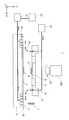
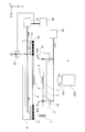
도 1은, 실시예 1에서의 임프린트 장치(1)의 개략 구성을 나타내는 도면이다. 이 임프린트 장치(1)는, 반도체 디바이스 등의 디바이스의 제조에 사용되어, 피처리 기판 위의 임프린트재(미경화 수지)를 형(몰드)으로 성형하고, 기판 위에 임프린트재의 패턴을 형성하는 장치이다. 여기에서는 임프린트재를 경화하는 방법으로서 광 경화법을 채용한 임프린트 장치로 하지만, 이에 한정되는 것은 아니다. 이하의 도면에서는, 기판 위의 임프린트재에 대해 자외선을 조사하는 조명계의 광축과 평행으로 Z축을 취하고, Z축에 수직인 평면 내에 있어서 서로 직교하는 X축 및 Y축을 취한다. 임프린트 장치(1)는, 조사부(100)와, 형 보유 지지부(4)와, 기판 스테이지(6)와, 공급부(7)를 구비한다.1 is a view showing a schematic structure of an
조사부(100)는, 임프린트 처리 시에, 임프린트재(8)에 대해 자외선(101)을 조사한다. 이 조사부(100)는, 도시되지 않지만, 노광 광원과, 이 노광 광원으로부터 조사된 자외선(101)을 임프린트에 적절한 광으로 조정하는 광학 소자로 구성된다. 임프린트재에는, 경화용 에너지가 부여됨으로써 경화되는 경화성 조성물(미경화 상태의 수지라 부르는 경우도 있음)이 사용된다. 경화용 에너지로는, 전자파, 열 등이 사용된다. 전자파로는, 예를 들어 그 파장이 10㎚ 이상 1㎜ 이하인 범위로부터 선택되는, 적외선, 가시광선, 자외선 등의 광이다.The
경화성 조성물은, 광의 조사에 의해, 혹은, 가열에 의해 경화되는 조성물이다. 이 중, 광에 의해 경화되는 광 경화성 조성물은, 중합성 화합물과 광중합 개시제를 적어도 함유하고, 필요에 따라 비중합성 화합물 또는 용제를 함유해도 된다. 비중합성 화합물은, 증감제, 수소 공여체, 내첨형 이형제, 계면 활성제, 산화 방지제, 중합체 성분 등의 군에서 선택되는 적어도 1종이다. 임프린트재는, 스핀 코터나 슬릿 코터에 의해 기판 위에 막 형상으로 부여된다. 혹은 액체 분사 헤드에 의해, 액적 형상, 혹은 복수의 액적이 연결되어 형성된 섬 형상 또는 막 형상으로 되어 기판 위에 부여되어도 된다. 임프린트재의 점도(25℃에서의 점도)는, 예를 들어 1mPa·s 이상 100mPa·s 이하이다.The curable composition is a composition which is cured by irradiation of light or by heating. Among them, the photocurable composition which is cured by light contains at least a polymerizable compound and a photopolymerization initiator, and may optionally contain a non-polymerizable compound or a solvent. The non-polymer compound is at least one member selected from the group consisting of a sensitizer, a hydrogen donor, an internal release agent, a surfactant, an antioxidant, and a polymer component. The imprint material is applied on the substrate in a film form by a spin coater or a slit coater. Or may be formed in a droplet shape or an island shape or a film shape in which a plurality of droplets are connected to each other by a liquid ejection head. The viscosity (viscosity at 25 캜) of the imprint material is, for example, 1 mPa · s or more and 100 mPa · s or less.
형(2)은, 외주 형상이 각형이며, 기판(5)에 대향하는 면은, 예를 들어 회로 패턴 등의 전사해야 할 요철 패턴이 3차원형으로 형성된 패턴부(3)를 포함한다. 형(2)의 재질은, 자외선(101)을 투과시키기가 가능한 재질이며, 본 실시예에서는 일례로서 석영으로 한다. 또한, 형(2)은, Z 방향의 변형을 용이하게 하기 위하여, 자외선(101)이 조사되는 면에, 어느 정도의 깊이를 갖는 캐비티(오목부)(9)가 형성된 형상으로 해도 된다.The
형 보유 지지부(4)는, 형(2)을 보유 지지하면서, 형(2)을 이동시키는 구동 기구를 갖는다. 형 보유 지지부(4)는, 형(2)에 있어서의 자외선(101)의 조사면의 외주 영역을 진공 흡착력이나 정전기의 힘에 의해 끌어 당김으로써 형(2)의 보유 지지가 가능하다. 예를 들어, 형 보유 지지부(4)가 진공 흡착력에 의해 형(2)을 보유 지지하는 경우에는, 형 보유 지지부(4)는, 외부에 설치된 도시되지 않은 진공 펌프에 접속되고, 이 진공 펌프의 ON/OFF에 의해 형(2)의 탈착이 전환된다. 형 보유 지지부(4)는, 형(2)과 기판(5) 위의 임프린트재(8)의 압박, 또는 분리를 행하도록 형(2)을 각 축 방향으로 이동시킨다. 이 형 보유 지지부(4)의 구동 기구로서 채용 가능한 액추에이터로서는, 예를 들어 리니어 모터 또는 에어 실린더가 있다. 또한, 이 구동 기구는, 형(2)의 고정밀도인 위치 결정에 대응하기 위하여, 조동 구동계나 미동 구동계 등의 복수의 구동계로 구성되어 있어도 된다. 또한, Z축 방향뿐만 아니라, X축 방향이나 Y축 방향 또는 θ 방향의 위치 조정 기능(회전 기구)이나, 형(2)의 기울기를 보정하기 위한 틸트 기능 등을 갖는 구성도 있을 수 있다. 또한, 임프린트 장치(1)에 있어서의 압박 및 분리 동작은, 형(2)을 Z축 방향으로 이동시킴으로써 실현해도 되지만, 기판 스테이지(6)를 Z축 방향으로 이동시킴으로써 실현해도 되거나 또는 그 양쪽을 상대적으로 이동시켜도 된다.The
기판(5)은, 유리, 세라믹스, 금속, 반도체, 수지 등이 사용되며, 필요에 따라, 그 표면에 기판과는 다른 재료를 포함하는 부재가 형성되어 있어도 된다. 기판(5)으로는, 구체적으로, 실리콘 웨이퍼, 화합물 반도체 웨이퍼, 석영 유리 등이다. 이 피처리면에는, 형(2)에 형성된 패턴부(3)에 의해 패턴 성형되는 자외선 경화형의 임프린트재(8)가 공급된다. 기판 스테이지(6)는, 기판(5)을 보유 지지하고, 형(2)과 기판(5) 위의 임프린트재(8)의 접촉 동작 시에 형(2)과 임프린트재(8)의 위치 정렬을 실시한다. 또한 기판 스테이지(6)는, 각 축방향으로 이동 가능하게 하는 스테이지 구동 기구(도시되지 않음)를 갖는다. 이 스테이지 구동 기구에 채용 가능한 액추에이터로서는, 예를 들어 리니어 모터나 평면 모터가 있다. 스테이지 구동 기구는, X축 및 Y축의 각 방향에 대해, 조동 구동계나 미동 구동계 등의 복수의 구동계로 구성되어 있어도 된다. 또한, Z축 방향의 위치 조정을 위한 구동계나, 기판(5)의 θ 방향의 위치 조정 기능(회전 기구) 또는 기판(5)의 기울기를 보정하기 위한 틸트 기능 등을 갖는 구성도 있을 수 있다.As the
공급부(7)는, 형 보유 지지부(4)의 근방에 설치되어, 기판(5) 위에 임프린트재(8)를 공급한다. 여기서, 이 임프린트재(8)는, 자외선(101)을 수광함으로써 경화하는 성질을 갖는 광 경화성 수지이며, 반도체 디바이스 제조 공정 등의 각종 조건에 의해 적절히 선택된다. 또한, 공급부(7)로부터 토출되는 임프린트재(8)의 양도, 기판(5) 위에 형성되는 임프린트재(8)가 원하는 두께나, 형성되는 패턴의 밀도 등에 의해 적절히 결정된다.The
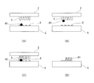
기판(5)에 임프린트재(8)가 공급되고, 형(2)과 기판(5)이 소정의 위치 관계에 위치 결정된 후, 형 보유 지지부(4)를 -Z 방향으로 이동하고, 패턴부(3)를 임프린트재(8)에 압박하여 기판(5) 위에 패턴을 형성한다. 여기서 도 2의 (A), 도 2의 (B)에 나타내는 바와 같이, 파티클(90)이 기판(5) 위의 압인 영역 내나 패턴부(3)에 부착된 상태에서, 패턴부(3)를 임프린트재(8)에 접촉시켜 버리면, 도 2의 (C)에 나타내는 바와 같이, 패턴부(3)가 파손될 가능성이 있다. 임프린트 장치는 반도체 디바이스를 제조하기 위한 청정한 환경 내에 놓이지만, 파티클의 발생을 없앤다는 것은 매우 곤란하다. 본 명세서에 있어서, 「파티클」이란, 패턴 형성에 관여하는 것을 목적으로 하지 않는 물질이다. 예를 들어, 공급부(7)로부터 토출된 임프린트재(8)가 떠돌아 건조된 고형물, 임프린트 장치(1)를 구성하는 부재로부터 발생되는 미립자, 외부로부터 진입하여 임프린트 장치(1) 내에 존재하는 티끌 등이다. 패턴 결함의 발생의 용이함은, 패턴부(3)의 패턴 치수나 패턴 깊이에 따라 상이하지만, 하프 피치 치수 이상의 크기의 파티클이 있으면 패턴 결함이 발생되기 쉬워진다.The
일단, 패턴부(3)가 파손되어 버리면 도 2의 (D)에 도시된 바와 같이, 그 이후, 기판(5) 위에 형성되는 모든 패턴(91)의 동일 장소에 결함이 발생되어 버려, 반도체 디바이스 제조의 수율이 현저하게 저하되어 버린다. 또한, 형(2)은 비교적 제조 비용이 높고, 반도체 디바이스의 비용 상승의 원인이 되어 버린다. 따라서, 임프린트 장치에서는, 파티클이 임프린트 공간에 끼어 들어, 기판(5)이나 패턴부(3)에 부착되는 것을 방지해야 한다. 또한, 이하의 설명에서, 임프린트 공간이란, 형(2)과 기판(5)이 대향했을 때에 형(2)과 기판(5) 사이에 생기는 공간을 의미한다. 종래의 임프린트 장치에서는, 도 3의 (A)에 나타내는 바와 같이, 기류 형성부(기류 형성 수단)인 기체 공급원(14)을 접속한 노즐(16)로부터 기판(5)을 향하여 기체(15)를 분사함으로써, 임프린트 장치의 외측으로 향하는 기류를 형성하고 있다. 즉, 스테이지(6)(기판(5))가 형(2)에 대향하고 있는 상태에서 기판(5)의 외주측을 따르는 방향으로 기류를 발생시킨다. 이에 따라, 파티클(90)이 임프린트 공간에 들어가는 것을 방지하고 있다. 노즐(16)은, 형(2)의 주위를 둘러싸도록 형 보유 지지부(4)에 설치된다. 노즐(16)로부터 기판(5)에 분사된 기체(15)는, 형(2)과 기판(5)에 끼워진 공간으로부터 임프린트 공간의 외부를 향하여, 하겐 포아젤· 흐름(Hagen-Poiseuille flow)이 되는 유속 분포(92)를 형성한다.Once the
그러나, 도 3의 (B)에 나타내는 바와 같이 기판 스테이지(6)가 이동할 때에는, 기판 스테이지(6)의 진행 방향의 전방에서는 유속 분포(93), 후방에서는 유속 분포(94)와 같이 변화된다. 유속 분포(94)의 기판 스테이지(6)의 표면 근방에서는, 외부로부터 임프린트 공간을 향하는 역류가 일부에 형성된다. 이것은, 일반적으로 기체를 포함하는 점성 유체에서는 벽면에 있어서 유속이 제로가 되기 때문에, 기판 스테이지(6)가 이동하면, 기판 스테이지(6)의 표면 근방의 기체도 기판 스테이지(6)와 함께 이동하고, 쿠에트 흐름(Couette flow)을 형성하기 때문이다. 외부로부터 임프린트 공간을 향하는 역류가 발생되면, 기판 스테이지(6)의 표면 근방에 존재하는 파티클(90)은 기판 스테이지(6)가 왕복 운동을 반복하는 동안에 임프린트 공간 속에 들어갈 가능성이 높아진다.However, when the
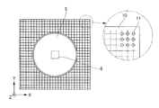
그래서, 도 1에 나타내는 실시예 1의 임프린트 장치에서는, 기판 스테이지(6)의 표면 근방의 파티클이 임프린트 공간에 진입하는 것을 방지하기 위한 다공판(10) 및 제어부(50)를 설치한다. 다수의 구멍(11)을 갖는 다공판(10)(판 부재)은, 기판 스테이지(6)의 기판(5)을 보유 지지하는 부분의 외주에 있는 외주부에 설치되어 있다. 다공판(10)에 접속된 진공원(흡인 수단)(12)이, 구멍(11)을 통하여 기판 스테이지 상의 공간의 기체(13)의 흡인을 행하고, 주변에 있는 파티클이 임프린트 공간에 진입하는 것을 방지한다. 다공판(10)에 형성된 다수의 구멍(11)은 기체의 흡인구 또는 방출구가 되는 구멍이다. 제어부(50)는, 공급부(7), 기판 스테이지(6), 조사부(100), 다공판(10)에 접속된 진공원(12)에 접속되어 있고, 이들을 제어하여 임프린트 처리를 실행한다. 제어부(50)는, 임프린트 처리에 관한 프로그램을 실행하는 CPU, 및 프로그램이나 각종 계측값 등을 기억하는 메모리를 포함한다. 도 4는, 형(2) 및 형 보유 지지부(4)를 -Z 방향으로부터 본 도면이다. 노즐(16)은, 형(2)을 둘러싸도록 환형으로 배치된다. 본 실시예에 있어서 노즐(16)은 1열이지만, 복수의 노즐(16)의 열이 동심원형으로 배치되어 있어도 된다. 또한, 1개의 노즐(16)의 형상이 원형이 아니고 슬릿형이어도 된다. 또한, 노즐(16)은, 이산적으로 형(2)의 주변에 배치되어 있어도 된다. 도 5는, 기판(5) 및 다공판(10)을 +Z 방향으로부터 본 도면이다. 본 실시예에 있어서 다공판(10)은, 기판(5)이 탑재되어 있는 부분을 제외한 기판 스테이지(6)의 상면 전체를 차지하고 있다. 다공판(10)은, 구멍(11)이 거의 균일하게 분포되어 있는 부재이다. 구멍(11)의 형상은 둥근 구멍에 한정되지 않고, 균일하게 흡인할 수 있는 형상이면 된다. 예를 들어, 도 6에 나타내는 바와 같이 기판(5)을 둘러싸는 슬릿(18)과 같은 형상이어도 된다. 다공판(10)의 재질은, 반도체 프로세스에 영향을 주지 않는 플라스틱, 세라믹스나 그것들의 다공질체가 적합하다.Thus, in the imprint apparatus of the first embodiment shown in Fig. 1, the
노즐(16)로부터 분출하는 기체(15)의 유량은 적절히 결정되지만, 임프린트 공간으로부터 외측으로 흐르는 평균 유속이 기판 스테이지(6)의 이동 속도의 최댓값보다도 큰 것이 바람직하다. 예를 들어, 형 보유 지지부(4)의 외주의 크기가 φ 320㎜, 임프린트 공간의 높이가 1㎜, 기판 스테이지(6)의 최대의 속도가 1m/s일 때, 기체(15)의 유량은 60L/min 이상이 바람직하다. 다공판(10)으로부터 흡인하는 기체(13)의 유량도 적절히 결정되지만, 기판 스테이지(6)의 외부에 부유하는 파티클(90)이, 역류를 타도 기판(5)에 도달하기 전에 다공판(10)으로부터 배출되는 유속으로 설정하면 된다. 상기한 예에서는, 역류 영역의 Z 방향 높이를 약170㎛, 기판(5)의 단으로부터 기판 스테이지(6)의 단까지 100㎜라 하면, 다공판(10)으로부터 흡인하는 기체(13)의 평균 유속은 1.7㎜/s 이상으로 하면 된다. 다공판(10)으로부터 흡인하는 기체(13)의 유량은, 다공판(10)과 진공원(12) 사이에 설치되고, 제어부(50)에 접속된, 도시되지 않은 유량 조정 수단에 의해 조정하면 된다.The flow rate of the
제어부(50)는, 도 7에 나타내는 바와 같이, 다공판(10)에 접속된 가압원(방출 수단)(19)과 접속되어도 된다. 이 경우, 다공판(10)이 임프린트 공간의 외부에 있을 때에 다공판(10)으로부터 기판 스테이지 상의 공간에 대해 기체(17)를 방출함으로써, 역류 영역에 들어온 파티클(90)은, 임프린트 공간으로부터 임프린트 공간의 외부로 배출된다.The
또한, 실시예 1의 임프린트 장치의 제어부(50)는, 도 8에 나타내는 바와 같이, 진공원(12)과 가압원(19) 양쪽의 전환을 행하는 전환 장치(전환부)(27)에 접속되어 있어도 된다. 전환 장치(27)는, 제어부(50)로부터의 지시에 기초하여, 기판 스테이지(6)의 위치 정보에 따라, 구멍(11)이 접속되는 선부를 진공원(11)과 가압원(12)으로 전환한다. 기체(13)의 흡인과 기체(17)의 방출을 전환할 수 있다. 흡인과 방출의 전환은, 예를 들어 다공판(10)의 접속처를, 기체를 흡인하는 경우는 진공원(12)으로 한다. 혹은, 다공판(10)의 접속처를, 기체를 방출하는 경우는 가압원(19)으로 한다. 예를 들어, 임프린트재(8)를 기판(5)에 공급하고, 패턴부(3)를 임프린트재(8)에 압박하는 동작을 반복하는 임프린트 공정의 사이는, 도 8의 (A)에 나타내는 바와 같이 진공원(12)에 접속하여, 기체(13)를 흡인한다. 한편, 기판 스테이지(6)가 형 보유 지지부(4) 하부로부터 어긋나서 기판(5)의 교환을 행하는 공정의 사이 등, 다공판(10)이 형과 대향하지 않은 상태에서, 도 8의 (B)에 나타내는 바와 같이 가압원(19)에 접속하고, 기체(17)를 방출한다. 이와 같이 구성함으로써, 기판 스테이지(6)가 형 보유 지지부(4) 하부로부터 어긋난 때에, 공기 중에 부유하는 파티클이 기판(5)에 부착되는 것을 억제하며, 또한, 임프린트 공정 중에 있어서도 파티클이 임프린트 공간에 들어가는 것을 억제할 수 있다. 기체(13)의 흡인과 기체(17)의 방출 유량은, 제어부(50)와 접속된 도시되지 않은 조정 수단에 의해 조정할 수 있다. 이상 설명한 대로 본 실시예 1에 의하면, 기판 스테이지(6) 표면 근방에 존재하는 파티클(90)이 기판 스테이지(6)의 이동에 수반하는 역류를 탔다고 해도, 임프린트 공간에 진입하는 파티클(90)의 수를 저감시킬 수 있다. 이에 의해, 패턴 결함 및 형(2)의 파손을 발생시키기 어렵게 할 수 있다.8, the
(실시예 2)(Example 2)
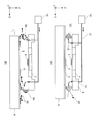
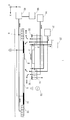
실시예 2의 임프린트 장치는, 임프린트 공간의 공기를 펜타플루오로프로판(PFP)이나 헬륨 가스 등의 치환 가스로 치환하는 기구를 갖는다. 이에 따라, 형의 요철 부분에의 임프린트재의 충전성이나, 이형의 용이함(임프린트재와 형의 분리하기 쉬움)을 향상시킬 수 있다. 본 실시예에서는, 외부에 부유하는 파티클(90)이 임프린트 공간에 들어가는 것을 억제하면서, 임프린트 공간의 치환 가스 농도를 충분히 유지하는 것이 가능한 임프린트 장치에 대해 설명한다.The imprint apparatus of the second embodiment has a mechanism for replacing air in the imprint space with replacement gas such as pentafluoropropane (PFP) or helium gas. This makes it possible to improve the filling property of the imprint material on the concavo-convex portion of the mold and the easiness of mold release (easiness of separation of imprint material and mold). In this embodiment, an imprint apparatus capable of sufficiently maintaining the concentration of the replacement gas in the imprint space while suppressing the entry of the
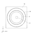
도 9는, 실시예 2에 있어서의 임프린트 장치(1)의 개략도이다. 치환 가스 공급원(21)은 치환 가스 공급부이며, 공급 노즐(22)로부터 임프린트 공간으로 치환 가스를 공급한다. 그리고, 임프린트 공간의 치환 가스는, 회수 노즐(24)을 통하여 치환 가스 회수부인 치환 가스 회수기(23)에 회수된다. 기판(5)을 보유 지지하는 영역을 제외한 기판 스테이지(6)의 상면에는, 기체의 흡인구 또한 방출구인 구멍을 갖는 판 부재가 설치된다. 본 실시예의 판 부재에는, 기판(5)에 인접하는 제1 영역에 다공판(25)이 설치되고, 다공판(25)의 기판(5)과 인접하지 않는 측의 제2 영역에 다공판(10)이 설치된다. 다공판(10, 25)은 각각 제어부(50)에 접속된 진공원(12)에 접속되어 있다. 진공원(12)으로부터 다공판(10, 25)까지의 기체의 유로에는, 다공판(10, 25)의 각각으로부터 흡인하는 기체의 흡인량을 제어 가능한 제어 밸브(20)가 설치되어 있다. 예를 들어, 제어부(50)는 제어 밸브(20)에도 접속되어 있고, 다공판(25)으로부터 흡인되는 기체의 유량을 제어할 수 있다.9 is a schematic view of the
기판(5)의 주변부에 임프린트재(8)를 공급하여 패턴을 형성할 경우, 임프린트 공간이 기판(5)과 다공판(25)의 양쪽을 포함하는 위치 관계가 되는 경우가 있다. 이 때, 다공판(25)으로부터 기체를 흡인하고 있으면, 치환 가스의 공급 회수의 균형이 깨지고, 파티클을 억제하기 위한 기체(15)를 임프린트 공간으로 유도되어 버린다. 이에 의해, 파티클 억제 효과가 저감될 뿐만 아니라, 임프린트 공간의 치환 가스 농도가 저하될 가능성이 있다. 따라서, 실시예 2의 임프린트 장치(1)에서는, 임프린트 공간이 기판(5)과 다공판(25)의 양쪽을 포함하는 위치 관계가 되는 경우에, 다공판(25)으로부터 기체의 흡인을 정지한다. 이에 의해, 파티클 억제 효과를 저감시키지 않고, 또한, 임프린트 공간의 치환 가스 농도를 높게 유지하는 것이 가능하다. 또한, 도 10에 도시하는 바와 같이, 제1 영역의 다공판(25) 부분을 구멍이 없는 단순한 판재(26)로 치환하여, 기체를 흡인하지 않도록 할 수도 있다. 이 경우, 파티클 억제 효과가 약간 저감되지만, 구성이 단순해지기 때문에 장치 비용을 저감시킬 수 있다.When the
상기 예에서는, 임프린트 공간이 기판(5)과 제1 영역의 양쪽을 포함하는 위치 관계가 되는 경우에 다공판(25) 또는 판재(26)를 통하여 기체의 흡인을 행하지 않는다. 그 때문에, 역류를 탄 파티클(90)을 회수하는 영역이 작아져, 파티클(90)이 임프린트 공간에 들어갈 가능성이 높아진다. 이에 반하여, 본 실시예 2의 다른 양태로서, 제1 영역을 또한 복수 영역으로 분할하고, 각각의 영역을 독립적으로 흡인할 수 있도록 구성한다. 도 11은, 제1 영역을 영역(251) 내지 영역(254)으로 4 분할한 예를 나타내고 있다. 제어 밸브(30)는, 영역(251) 내지 영역(254)으로부터의 기체의 흡인량(기체의 유량)을 개별로 제어하기 위한 제어 밸브이다. 도 11에서는, 임프린트재(8)가 기판(5)의 -X측 단부면에 공급된 상태에서 패턴을 형성하는 경우를 나타내고 있다. 이 때, 임프린트 공간은 기판(5)과 영역(251)을 포함한 위치 관계로 되기 때문에, 제어 밸브(30)를 조작하여 영역(251)으로부터의 기체의 흡인만을 정지한다. 이와 같이 상기 제1 영역을 분할한 각각의 영역으로부터의 기체의 흡인을 개별로 행하도록 함으로써, 역류를 탄 파티클(90)을 회수하는 영역의 축소를 최소한으로 억제할 수 있고, 파티클(90)이 임프린트 공간에 들어갈 가능성을 낮게 유지할 수 있다. 이에 따라, 임프린트 공간에 진입하는 파티클(90)의 수를 저감시켜, 패턴 결함 및 형(2)의 파손을 발생시키기 어렵게 할 수 있다.In this example, when the imprint space is in a positional relationship including both the
(실시예 3)(Example 3)
임프린트 장치(1)에서는, 형(2)과 경화된 임프린트재(8)를 분리했을 때 패턴부(3)가 대전되기 쉬워지는 것이 알려져 있다. 또한, 패턴부(3)가 대전함으로써 주위의 파티클을 끌어 모으기 쉬워져 버린다. 예를 들어 도 8의 (B)에 나타내는 바와 같이 기판 스테이지(6)가 형(2)으로부터 이격되어 있는 상태라 해도, 부유하고 있는 파티클이 형(2)의 패턴부(3)에 끌어 모아져, 부착될 가능성이 있다.In the
실시예 3에 관한 임프린트 장치(1)는, 형(2)의 패턴부(3)에 부착된 파티클을 제거, 혹은 임프린트 공간의 내외를 부유하는 파티클을 포착하는 포착 수단을 갖는다. 도 12는, 실시예 3에 있어서의 임프린트 장치(1)의 구성을 나타내는 도면이다. 본 실시 형태의 임프린트 장치(1)의 구성은, 실시예 1에 관한 임프린트 장치(1)의 구성과 다공판(10) 이외의 구성은 동일하고, 이미 설명한 구성의 상세한 설명은 생략한다. 다공판(34)은, 전술한 다공판(10)과 동일하게 복수의 구멍(11)을 가지며, 또한 형(2)과 대향 가능한 면이 도전성의 재질로 구성되어 있다. 다공판(34)은 전원(35)과 접속되어 있음으로써, 전극부로서 기능한다. 다공판(34)은, 전체가 전극부로서 기능해도 되고, 일부가 전극부로서 기능해도 된다. 또한, 다공판(34)의 표면은 도시되지 않은 절연 피막에 의해 보호되어도 된다. 다공판(34)은 전원(35)에 접속되고, 전원(35)의 다른 쪽은 접지되어 있다.The
전원(35)의 다공판(34)측의 극성은 도 12에 있어서는 플러스로 되어 있지만, 패턴부(3)의 대전 극성에 따라서는 마이너스로 해도 된다. 또한 전원(35)은, 직류 전압을 인가하는 직류 전원에 한정되지 않고 교류 전압을 인가하는 교류 전원으로 해도 된다. 또는 직류 전압과 교류 전압이 전환되는 전원이어도 된다. 제어부(50)가 전원(35)을 제어함으로써, 다공판(34)의 표면 전위를 제어할 수 있다.The polarity of the
또한, 실시예 3에 관한 임프린트 장치(1)는, 형(2)을 제전하기 위한 제전 장치(도시되지 않음)를 갖는 것이 바람직하다. 제전 장치로서는, 코로나 방전식 또는 연X선이나 α선 등의 전리 방사선식이 채용된다. 제전 장치에 의해, 형(2)을 제전함으로써, 비교적 작은 값까지 패턴부(3)의 전위를 낮출 수 있다.It is preferable that the
도 13은, 파티클(90)이 부착된 형의 패턴부(3)에 다공판(34)을 근접하여 대향시킨 부분의 확대도이다. 패턴부(3)는 제전 장치에 의해 제전되어 있으므로, 파티클(90)과 패턴부(3)의 부착력은 비교적 작게(반데르발스힘 정도) 되어 있다. 다공판(34)을 형(2)과 같은 극성으로 해 둠으로써, 파티클(90)은 비교적 작은 외력으로 패턴부(3)로부터 분리할 수 있다. 패턴부(4)로부터 분리된 파티클(90)은, 다공판(34)에 끌어 모아진다. 끌어 모아진 후는 주위의 기체를 흡인하고 있는 구멍(11)을 통하여 진공원(12)으로 회수되거나, 또는 다공판(34)의 표면에 포착된다.Fig. 13 is an enlarged view of a portion where the
또한, 대전된 다공판(34)은, 전하를 띤 파티클뿐만 아니라, 전하를 갖지 않는 파티클도 끌어 모아진다. 다공판(34)이 형성하는 전계의 비균일성에서 유래하는 전계 구배력에 의해 파티클(90)이 패턴부(3)로부터 이격되기 때문이다.In addition, the charged
이에 의해, 본 실시 형태의 임프린트 장치(1)는, 실시예 1의 경우보다도 더욱 파티클(90)을 강하게 끌어 모을 수 있다. 패턴부(3)에 부착된 파티클도 회수할 수 있다. 이에 따라, 패턴 결함 및 패턴부(3)에의 끼임에 의한 형(2)의 파손을 발생시키기 어렵게 할 수 있다.Thereby, the
또한, 본 실시 형태의 임프린트 장치(1)는, 패턴부(3)의 전위를 계측하는 전위계(도시되지 않음)를 갖고 있어도 된다. 이에 따라, 정기적으로 전위를 계측한 결과에 기초하여, 제어부(50)가, 다공판(34)에 부여하는 전압의 극성이나 크기를 제어해도 된다.The
(실시예 4)(Example 4)
다공판(10)의 구멍(11)이 형성되지 않은 부분에 파티클이 부착된 경우, 형(2)의 근처를 통과했을 때 다공판(10)으로부터 패턴부에 파티클이 끌어 모아질 가능성이 있다. 예를 들어, 도 10에 나타내는 바와 같은 형(2)과 기판 스테이지(6)의 위치 관계보다 더욱 기판 스테이지(6)가 노즐(16) 하부로부터 이격되어, 기체(15)가 판재(26) 위를 흐르지 않게 되면, 공간에 부유하고 있는 파티클이 판재(26)에 부착될 가능성이 있다. 판재(26)는, 스루풋의 관점에서 빈번히 교환하는 것이 아니기 때문에, 파티클이 부착되어 있을 가능성이 비교적 높다. 판재(26)의 표면에 일단 파티클이 부착되면, 판재(26)의 표면은 기체(15)의 흐름이 거의 0이 되기 때문에, 기체(15)에 의해 판재(26) 표면으로부터 파티클을 제거하기가 곤란해진다. 본 발명의 실시예 4에서는, 판재(26)에 부착된 파티클을 제거하기 위한 제거 수단을 갖는다.There is a possibility that particles are attracted to the pattern portion from the
도 14는, 실시예 4에 관한 임프린트 장치(1)의 구성을 나타내는 도면이다. 임프린트 장치(1)는, 기판 스테이지(6)에는, 전기적으로 접지된 도전성의 판재(31)를 갖는다. 판재(31)는, 다공판(10)보다도 기판(5)이 배치되는 부분에 가까운 측에 배치되어 있는 것이 바람직하다. 이와 같이 구성함으로써, 후술하는 구성에 의해 판재(31)로부터 이탈하고, 노즐(16)로부터의 기체의 흐름을 타고 운반된 파티클(90)을, 다공판(10)에 의해 회수하기 쉽게 할 수 있다. 또한, 판재(31)의 표면은 도시되지 않은 절연 피막에 의해 보호되어도 된다.Fig. 14 is a diagram showing the configuration of the
한편, 형(2)의 노즐(16)보다도 형(2)에 대해 외측에는 전원(33)에 접속된 도전성의 전극(32)이 설치되어 있다. 전원(33)의, 전극(32)과 접속되지 않은 쪽의 단자는 전기적으로 접지되어 있다. 전원(33)은, 정현파, 구형파, 삼각파, 톱니파 등 시간적으로 변화하는 교류 성분을 포함하는 전압을 전극(32)에 부여하기 위한 전원이다. 전극(32)과 판재(31)가 대향하면, 시간적으로 크기가 변동하는 전계가 형성된다. 또한, 전극(32)에 의해 형성되는 전계는, 그 방향이 시간적으로 역전하는 전계여도 되고, 일정한 방향으로 크기만이 변동하는 전계여도 된다. 전계의 방향은, 형(2)의 전위에 따른 전계의 방향과 동일한 방향으로 해도 된다. 형(2)의 전위는, 실시예 3과 동일하게 전위계(도시되지 않음)에 의해 계측될 수 있다.On the other hand, a
다음에, 판재(31)에 부착된 파티클(90)의 제거 방법에 대해 설명한다. 도 15는, 패턴부(3)와 임프린트재(8)를 분리한 직후의 모습을 나타내고 있다. 도 15에 나타내는 패턴부(3) 및 임프린트재(8)의 극성은, 패턴부(3) 및 임프린트재(8)의 재질에 따라 변화할 수 있다. 패턴부(3)의 대전 전위(Vp)는 도시되지 않은 전위계로 그때마다 계측하거나, 미리 실험하여 전위 계측한 결과에 의해 기지로 한다.Next, a method of removing the
도 15에 나타내는 상태 후에, 다음 패턴을 형성할 위치에 공급부(7)로부터 임프린트재(8)를 부여하기 위하여, 기판 스테이지(6)는 X 방향으로 이동한다. 기판 스테이지(6)의 이동에 의해 전극(32)과 판재(31)가 적어도 대향하고 있는 기간에, 전원(33)은 전극(32)에 패턴부(3)의 대전 극성과 동극으로, 또한 패턴부(3)의 대전 전위(Vp)의 절댓값보다 큰 전위(Ve)를 인가한다. 즉, |Ve|>|Vp|가 되는 전위를 전극(32)과 판재(31)가 대향하고 있는 동안에 전극(32)에 적어도 1회 이상 인가한다. 이에 의해, 판재(31) 위에 부착되어 있는 파티클(90) 중, 이탈되기 쉬운 파티클(90)은, 전극(32)과 판재(31) 사이에 형성된 전계로부터 힘을 받아서 판재(31) 위로부터 이격된다. 판재(31)로부터 이격된 파티클(90)은 기체(15)의 흐름에 운반되고, 주위의 기체를 흡인하고 있는 다공판(10)을 통하여 진공원(12)에 회수된다.After the state shown in Fig. 15, the
한편, 판재(31)에 부착된 채로 있는 파티클(90)은, 미리 |Ve|>|Vp|가 되는 전위를 부여해도 판재(31)로부터 이격되지 않은 것이다. 따라서, 기판 스테이지(6)의 이동에 의해 패턴부(3) 하부를 통과해도, 파티클(90)이 판재(31)로부터 이격되어 패턴부(3)에 부착될 가능성은 낮다.On the other hand, the
이와 같이, 전원(33)을 사용하여 전극(32)에 교류 성분을 포함하는 전압을 인가함으로써, 판재(31)에 부착된 비교적 이탈하기 쉬운 파티클을 판재(31) 상으로부터 제거할 수 있다. 이에 의해, 판재(31)로부터 의도하지 않은 타이밍에 이격된 파티클(90)이 패턴부(3)에 부착되기 어렵게 할 수 있다. 따라서, 임프린트 처리 시의 패턴 결함의 발생이나 형(2)의 파손 발생을 억제할 수 있다.As described above, by applying the voltage including the AC component to the
전극(32)은, 형 보유 지지부(4)를 -Z 방향으로부터 보았을 때, 환형으로 배치되어 있어도 되고, 이산적으로 배치되어 있어도 된다. 형 보유 지지부(4) 중, 공급부(7)로부터 먼 측의 적어도 일부에 설치되어 있는 것이 바람직하다. 당해 적어도 일부는, 기판 스테이지(6)가 공급부(7) 하부로 향할 때에 판재(31)에 반드시 대향하는 부분이며, 판재(31)에 부착된 파티클이 형(2)에 가까이 가기 전에 이탈시키는 것이 바람직하기 때문이다.The
(물품의 제조 방법에 관한 실시예)(Example of Manufacturing Method of Articles)
임프린트 장치를 사용하여 형성된 경화물의 패턴은, 각종 물품의 적어도 일부에 영구적으로, 혹은 각종 물품을 제조할 때에 일시적으로, 사용될 수 있다. 물품이란, 전기 회로 소자, 광학 소자, MEMS, 기록 소자, 센서, 혹은, 형 등이다. 전기 회로 소자로서는, DRAM, SRAM, 플래시 메모리, MRAM과 같은, 휘발성 혹은 불휘발성 반도체 메모리나, LSI, CCD, 이미지 센서, FPGA와 같은 반도체 소자 등을 들 수 있다. 형으로는, 임프린트용 몰드 등을 들 수 있다.The pattern of the cured product formed by using the imprint apparatus can be used permanently on at least a part of various articles or temporarily when manufacturing various articles. An article is an electric circuit element, an optical element, a MEMS, a recording element, a sensor, or a mold. Examples of the electric circuit element include a volatile or nonvolatile semiconductor memory such as a DRAM, an SRAM, a flash memory, and an MRAM, and a semiconductor element such as an LSI, a CCD, an image sensor, and an FPGA. Examples of the mold include an imprint mold and the like.
경화물의 패턴은, 상기 물품의 적어도 일부의 구성 부재로서, 그대로 사용되거나, 혹은, 레지스트 마스크로서 일시적으로 사용된다. 기판의 가공 공정에서 에칭 또는 이온 주입 등이 행해진 후, 레지스트 마스크는 제거된다.The pattern of the cured product is used as a constituent member of at least a part of the article as it is, or temporarily used as a resist mask. After etching or ion implantation or the like is performed in the processing step of the substrate, the resist mask is removed.
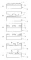
이어서, 물품의 구체적인 제조 방법에 대해 설명한다. 도 16의 (A)에 나타내는 바와 같이, 절연체 등의 피가공재(5z)가 표면에 형성된 실리콘 웨이퍼 등의 기판(5)을 준비하고, 계속해서, 잉크젯법 등에 의해, 피가공재(5z)의 표면에 임프린트재(8)를 부여한다. 여기에서는, 복수의 액적 형상으로 된 임프린트재(8)가 기판 위에 부여된 모습을 나타내고 있다.Next, a specific manufacturing method of the article will be described. As shown in Fig. 16A, a
도 16의 (B)에 나타내는 바와 같이, 임프린트용의 형(2)을, 그 요철 패턴이 형성된 측을 기판 위의 임프린트재(8)를 향해, 대향시킨다. 도 16의 (C)에 나타내는 바와 같이, 임프린트재(8)가 부여된 기판(1)과 형(2)을 접촉시켜서, 압력을 가한다. 임프린트재(8)는 형(2)과 피가공재(5z)의 간극에 충전된다. 이 상태에서 경화용 에너지로서 광을 형(2)을 투과하여 조사하면, 임프린트재(8)는 경화된다.As shown in Fig. 16B, the
도 16의 (D)에 나타내는 바와 같이, 임프린트재(8)를 경화시킨 후, 형(2)과 기판(5)을 분리하면, 기판(5) 위에 임프린트재(8)의 경화물 패턴이 형성된다. 이 경화물의 패턴은, 형의 오목부가 경화물의 볼록부에, 형의 오목부가 경화물의 볼록부에 대응한 형상으로 되어 있고, 즉, 임프린트재(8)에 형(2)의 요철 패턴이 전사되게 된다.16 (D), when the
도 16의 (E)에 나타내는 바와 같이, 경화물의 패턴을 내에칭 마스크로 하여 에칭을 행하면, 피가공재(5z)의 표면 중, 경화물이 없거나 혹은 얇게 잔존한 부분이 제거되어, 홈(5z)으로 된다. 도 16의 (F)에 나타내는 바와 같이, 경화물의 패턴을 제거하면, 피가공재(5z)의 표면에 홈(5z)이 형성된 물품을 얻을 수 있다. 여기에서는 경화물의 패턴을 제거했지만, 가공 후에도 제거하지 않고, 예를 들어 반도체 소자 등에 포함되는 층간 절연용의 막, 즉, 물품의 구성 부재로서 이용해도 된다.16 (E), etching is performed using a pattern of the cured product as an inner etching mask to remove portions of the surface of the material to be processed 5z from which no cured product is present or remaining thinly. As a result, . As shown in FIG. 16F, when the pattern of the cured product is removed, an article in which the
이상, 본 발명의 바람직한 실시예에 대해 설명했지만, 본 발명은 이들 실시예에 한정되지 않고, 그 요지의 범위 내에서 다양한 변형 및 변경이 가능하다.Although the preferred embodiments of the present invention have been described above, the present invention is not limited to these embodiments, and various modifications and changes may be made within the scope of the present invention.
1: 임프린트 장치
2: 형
4: 형 보유 지지부
5: 기판
6: 스테이지
8: 임프린트재
10: 다공판
12: 진공원1: Imprint device
2: Type
4:
5: substrate
6: stage
8: Imprint material
10: Perforated plate
12: Vacuum source
Claims (15)
상기 기판을 보유 지지하여 이동 가능한 스테이지와,
상기 스테이지 위의 상기 기판을 보유 지지하는 부분의 외주부에 배치되고, 구멍을 갖는 판 부재와,
상기 구멍을 통하여 상기 스테이지 상의 공간의 기체를 흡인하는 흡인 수단과,
상기 구멍을 통하여 상기 스테이지 상의 공간에 기체를 방출하는 방출 수단과,
상기 구멍의 접속처를 상기 흡인 수단 또는 상기 방출 수단으로 전환하는 전환부를 갖는
것을 특징으로 하는 임프린트 장치.An imprint apparatus for forming a pattern of an imprint material on a substrate using a mold,
A stage capable of holding and moving the substrate,
A plate member disposed on an outer periphery of a portion for holding the substrate on the stage, the plate member having a hole;
A suction means for sucking the gas in the space on the stage through the hole,
Releasing means for releasing gas into the space on the stage through the hole,
And a switching portion for switching the connection destination of the hole to the suction means or the discharging means
And the imprint apparatus.
상기 제어부는, 상기 스테이지의 위치 정보에 기초하여 상기 구멍의 접속처를 전환하는 것을 특징으로 하는 임프린트 장치.2. The image processing apparatus according to claim 1, further comprising a control unit for controlling the switching unit,
Wherein the control unit switches the connection destination of the hole based on the position information of the stage.
상기 기류 형성 수단은, 상기 방출 수단으로부터 방출된 기체를 상기 기판의 외주측을 따르는 방향으로 흘리는 것을 특징으로 하는 임프린트 장치.2. The apparatus according to claim 1, further comprising air flow forming means for jetting a gas from the periphery of the mold and generating an air flow in a direction along the outer peripheral side of the substrate in a state in which the substrate faces the mold,
Wherein the airflow forming means is configured to flow the gas emitted from the discharging means in a direction along the outer peripheral side of the substrate.
상기 흡인 수단은, 상기 판 부재의 제1 영역의 상기 구멍으로부터 상기 기체를 흡인하는 제1 흡인부와, 상기 판 부재의 제2 영역의 상기 구멍으로부터 상기 기체를 흡인하는 제2 흡인부를 포함하고,
상기 흡인 제어부는, 상기 제1 흡인부와 상기 제2 흡인부와 각각이 흡인하는 기체의 유량 및 타이밍의 적어도 한쪽을 제어하는 것을 특징으로 하는 임프린트 장치.The apparatus according to claim 1, further comprising a suction control unit for controlling at least one of a flow rate and a timing of a gas sucked by said suction means,
Wherein the suction unit includes a first suction unit for sucking the gas from the hole in the first area of the plate member and a second suction unit for sucking the gas from the hole in the second area of the plate member,
Wherein the suction control unit controls at least one of a flow rate and a timing of a gas sucked by the first suction unit and the second suction unit, respectively.
상기 방출 수단은, 상기 판 부재의 제1 영역의 상기 구멍으로부터 상기 기체를 방출하는 제1 방출부와, 상기 판 부재의 제2 영역의 상기 구멍으로부터 상기 기체를 방출하는 제2 방출부를 포함하고,
상기 방출 제어부는, 상기 제1 방출부와 상기 제2 방출부의 각각이 흡인하는 기체의 유량 및 타이밍의 적어도 한쪽을 제어하는 것을 특징으로 하는 임프린트 장치.The apparatus according to claim 1, further comprising a discharge control section for controlling at least one of a flow rate and a timing of a gas discharged from said discharge means,
The release means comprising a first discharge portion for discharging the gas from the hole in the first region of the plate member and a second discharge portion for discharging the gas from the hole in the second region of the plate member,
Wherein the emission control unit controls at least one of a flow rate and a timing of a gas sucked by each of the first emitting unit and the second emitting unit.
상기 전극부에 직류 전압을 인가하는 전원을 갖고,
상기 직류 전압을 사용하여 상기 전극은 상기 스테이지 상의 파티클을 끌어 모으는 것을 특징으로 하는 임프린트 장치.The plasma display apparatus according to claim 1, further comprising: an electrode section provided on the stage;
And a power source for applying a DC voltage to the electrode unit,
And the electrode pulls the particles on the stage using the DC voltage.
상기 스테이지 위에 설치된 제2 전극부와,
상기 제1 전극부와 상기 제2 전극부 사이에 교류 성분을 포함하는 전압을 인가하는 전원을 포함하고,
상기 전원을 사용하여 상기 제1 전극부에서 파티클을 이탈시켜,
상기 흡인 수단은, 상기 이탈시킨 파티클을 상기 기체와 함께 상기 구멍을 통하여 흡인하는 것을 특징으로 하는, 임프린트 장치.2. The device according to claim 1, further comprising: a first electrode portion provided on a portion of the mold holding portion that is opposed to the stage;
A second electrode portion provided on the stage,
And a power source for applying a voltage including an AC component between the first electrode unit and the second electrode unit,
The particles are separated from the first electrode unit using the power source,
And the suction means sucks the separated particle through the hole with the base.
상기 공정에서 상기 패턴이 형성된 상기 기판을 처리하는 공정을 갖고,
상기 임프린트 장치는,
상기 기판을 보유 지지하여 이동 가능한 스테이지와,
상기 스테이지 위의 상기 기판을 보유 지지하는 부분의 외주부에 배치되고, 구멍을 갖는 판 부재와,
상기 구멍을 통하여 상기 스테이지 상의 공간의 기체를 흡인하는 흡인 수단과,
상기 구멍을 통하여 상기 스테이지 상의 공간에 기체를 방출하는 방출 수단과,
상기 구멍의 접속처를 상기 흡인 수단 또는 상기 방출 수단으로 전환하는 전환부
를 갖는 것을 특징으로 하는 물품의 제조 방법.A step of forming the pattern on the substrate by using an imprint apparatus which forms a pattern on a substrate using a mold,
And a step of processing the substrate on which the pattern is formed in the step,
The imprint apparatus includes:
A stage capable of holding and moving the substrate,
A plate member disposed on an outer periphery of a portion for holding the substrate on the stage, the plate member having a hole;
A suction means for sucking the gas in the space on the stage through the hole,
Releasing means for releasing gas into the space on the stage through the hole,
And a switching unit for switching the connection destination of the hole to the suction unit or the discharge unit
≪ / RTI >
Applications Claiming Priority (5)
| Application Number | Priority Date | Filing Date | Title |
|---|---|---|---|
| JP2016018746 | 2016-02-03 | ||
| JPJP-P-2016-018746 | 2016-02-03 | ||
| JP2016240689A JP2017139452A (en) | 2016-02-03 | 2016-12-12 | Imprint apparatus and method of manufacturing article |
| JPJP-P-2016-240689 | 2016-12-12 | ||
| PCT/JP2017/000578 WO2017134989A1 (en) | 2016-02-03 | 2017-01-11 | Imprinting device, and article production method |
Publications (1)
| Publication Number | Publication Date |
|---|---|
| KR20180098626A true KR20180098626A (en) | 2018-09-04 |
Family
ID=59565103
Family Applications (1)
| Application Number | Title | Priority Date | Filing Date |
|---|---|---|---|
| KR1020187021645A Abandoned KR20180098626A (en) | 2016-02-03 | 2017-01-11 | Imprint apparatus and method of manufacturing article |
Country Status (3)
| Country | Link |
|---|---|
| JP (1) | JP2017139452A (en) |
| KR (1) | KR20180098626A (en) |
| TW (1) | TWI618116B (en) |
Cited By (1)
| Publication number | Priority date | Publication date | Assignee | Title |
|---|---|---|---|---|
| KR20210032907A (en) * | 2019-09-17 | 2021-03-25 | 캐논 가부시끼가이샤 | Imprint apparatus and article manufacturing method |
Families Citing this family (4)
| Publication number | Priority date | Publication date | Assignee | Title |
|---|---|---|---|---|
| JP7064310B2 (en) * | 2017-10-24 | 2022-05-10 | キヤノン株式会社 | Imprinting equipment and article manufacturing method |
| JP7077754B2 (en) * | 2018-05-08 | 2022-05-31 | 大日本印刷株式会社 | Imprint mold substrate, imprint mold and their manufacturing method |
| JP7495814B2 (en) * | 2020-05-13 | 2024-06-05 | キヤノン株式会社 | Imprinting apparatus and method for manufacturing article |
| JP7579092B2 (en) * | 2020-09-11 | 2024-11-07 | キヤノン株式会社 | Foreign object removal apparatus, lithography apparatus, and article manufacturing method |
Citations (1)
| Publication number | Priority date | Publication date | Assignee | Title |
|---|---|---|---|---|
| JP2014056854A (en) | 2012-09-11 | 2014-03-27 | Dainippon Printing Co Ltd | Imprint method and imprint device for implementing the same |
Family Cites Families (3)
| Publication number | Priority date | Publication date | Assignee | Title |
|---|---|---|---|---|
| JP2731950B2 (en) * | 1989-07-13 | 1998-03-25 | キヤノン株式会社 | Exposure method |
| JP2002069634A (en) * | 2000-08-29 | 2002-03-08 | Canon Inc | Thin film manufacturing method and thin film manufacturing apparatus |
| JP6399839B2 (en) * | 2014-07-15 | 2018-10-03 | キヤノン株式会社 | Imprint apparatus and article manufacturing method |
-
2016
- 2016-12-12 JP JP2016240689A patent/JP2017139452A/en active Pending
-
2017
- 2017-01-11 KR KR1020187021645A patent/KR20180098626A/en not_active Abandoned
- 2017-01-19 TW TW106101896A patent/TWI618116B/en not_active IP Right Cessation
Patent Citations (1)
| Publication number | Priority date | Publication date | Assignee | Title |
|---|---|---|---|---|
| JP2014056854A (en) | 2012-09-11 | 2014-03-27 | Dainippon Printing Co Ltd | Imprint method and imprint device for implementing the same |
Cited By (1)
| Publication number | Priority date | Publication date | Assignee | Title |
|---|---|---|---|---|
| KR20210032907A (en) * | 2019-09-17 | 2021-03-25 | 캐논 가부시끼가이샤 | Imprint apparatus and article manufacturing method |
Also Published As
| Publication number | Publication date |
|---|---|
| TW201729251A (en) | 2017-08-16 |
| TWI618116B (en) | 2018-03-11 |
| JP2017139452A (en) | 2017-08-10 |
Similar Documents
| Publication | Publication Date | Title |
|---|---|---|
| JP6661397B2 (en) | Imprint apparatus, imprint method, and article manufacturing method | |
| KR20180098626A (en) | Imprint apparatus and method of manufacturing article | |
| JP6603678B2 (en) | Imprint apparatus, operation method thereof, and article manufacturing method | |
| JP6725046B2 (en) | Imprint apparatus, imprint method, and control method for imprint apparatus | |
| KR20150143321A (en) | Imprint method, imprint apparatus, and article manufacturing method | |
| KR102383372B1 (en) | Lithography apparatus and method of manufacturing article | |
| WO2016170729A1 (en) | Imprint apparatus, method of imprinting, and method of manufacturing article | |
| JP6789772B2 (en) | Imprint equipment, imprint method and article manufacturing method | |
| KR20150143320A (en) | Imprint apparatus, imprint method, method of manufacturing article, and supply apparatus | |
| KR102206846B1 (en) | Imprint apparatus and article manufacturing method | |
| US10777443B2 (en) | Imprint apparatus, imprinting method, and method for manufacturing article | |
| KR102294037B1 (en) | Imprint apparatus, and method of manufacturing article | |
| TWI680050B (en) | Imprint device, operation method thereof, and article manufacturing method | |
| JP2019067916A (en) | Lithographic apparatus and method of manufacturing article | |
| WO2016052345A1 (en) | Imprinting device, imprinting method, and control method for imprinting device | |
| JP7089420B2 (en) | Substrate processing equipment and article manufacturing method | |
| KR20170054455A (en) | Imprint apparatus, imprint method, and article manufacturing method | |
| WO2017134989A1 (en) | Imprinting device, and article production method | |
| JP7495814B2 (en) | Imprinting apparatus and method for manufacturing article | |
| KR20190018391A (en) | Imprint apparatus, and method of manufacturing article | |
| KR20230122983A (en) | Imprint apparatus, foreign particle removal method, and article manufacturing method |
Legal Events
| Date | Code | Title | Description |
|---|---|---|---|
| A201 | Request for examination | ||
| PA0105 | International application |
St.27 status event code: A-0-1-A10-A15-nap-PA0105 |
|
| PA0201 | Request for examination |
St.27 status event code: A-1-2-D10-D11-exm-PA0201 |
|
| PG1501 | Laying open of application |
St.27 status event code: A-1-1-Q10-Q12-nap-PG1501 |
|
| E902 | Notification of reason for refusal | ||
| PE0902 | Notice of grounds for rejection |
St.27 status event code: A-1-2-D10-D21-exm-PE0902 |
|
| P11-X000 | Amendment of application requested |
St.27 status event code: A-2-2-P10-P11-nap-X000 |
|
| P13-X000 | Application amended |
St.27 status event code: A-2-2-P10-P13-nap-X000 |
|
| E701 | Decision to grant or registration of patent right | ||
| PE0701 | Decision of registration |
St.27 status event code: A-1-2-D10-D22-exm-PE0701 |
|
| PC1904 | Unpaid initial registration fee |
St.27 status event code: A-2-2-U10-U14-oth-PC1904 St.27 status event code: N-2-6-B10-B12-nap-PC1904 |
|
| P22-X000 | Classification modified |
St.27 status event code: A-2-2-P10-P22-nap-X000 |