KR20180098447A - 유기 발광 표시 장치 - Google Patents
유기 발광 표시 장치 Download PDFInfo
- Publication number
- KR20180098447A KR20180098447A KR1020170024953A KR20170024953A KR20180098447A KR 20180098447 A KR20180098447 A KR 20180098447A KR 1020170024953 A KR1020170024953 A KR 1020170024953A KR 20170024953 A KR20170024953 A KR 20170024953A KR 20180098447 A KR20180098447 A KR 20180098447A
- Authority
- KR
- South Korea
- Prior art keywords
- light emitting
- conductive member
- disposed
- pixel
- planarization
- Prior art date
- Legal status (The legal status is an assumption and is not a legal conclusion. Google has not performed a legal analysis and makes no representation as to the accuracy of the status listed.)
- Granted
Links
Images


Classifications
-
- H01L27/3248—
-
- G—PHYSICS
- G09—EDUCATION; CRYPTOGRAPHY; DISPLAY; ADVERTISING; SEALS
- G09G—ARRANGEMENTS OR CIRCUITS FOR CONTROL OF INDICATING DEVICES USING STATIC MEANS TO PRESENT VARIABLE INFORMATION
- G09G3/00—Control arrangements or circuits, of interest only in connection with visual indicators other than cathode-ray tubes
- G09G3/20—Control arrangements or circuits, of interest only in connection with visual indicators other than cathode-ray tubes for presentation of an assembly of a number of characters, e.g. a page, by composing the assembly by combination of individual elements arranged in a matrix no fixed position being assigned to or needed to be assigned to the individual characters or partial characters
- G09G3/22—Control arrangements or circuits, of interest only in connection with visual indicators other than cathode-ray tubes for presentation of an assembly of a number of characters, e.g. a page, by composing the assembly by combination of individual elements arranged in a matrix no fixed position being assigned to or needed to be assigned to the individual characters or partial characters using controlled light sources
- G09G3/30—Control arrangements or circuits, of interest only in connection with visual indicators other than cathode-ray tubes for presentation of an assembly of a number of characters, e.g. a page, by composing the assembly by combination of individual elements arranged in a matrix no fixed position being assigned to or needed to be assigned to the individual characters or partial characters using controlled light sources using electroluminescent panels
- G09G3/32—Control arrangements or circuits, of interest only in connection with visual indicators other than cathode-ray tubes for presentation of an assembly of a number of characters, e.g. a page, by composing the assembly by combination of individual elements arranged in a matrix no fixed position being assigned to or needed to be assigned to the individual characters or partial characters using controlled light sources using electroluminescent panels semiconductive, e.g. using light-emitting diodes [LED]
- G09G3/3208—Control arrangements or circuits, of interest only in connection with visual indicators other than cathode-ray tubes for presentation of an assembly of a number of characters, e.g. a page, by composing the assembly by combination of individual elements arranged in a matrix no fixed position being assigned to or needed to be assigned to the individual characters or partial characters using controlled light sources using electroluminescent panels semiconductive, e.g. using light-emitting diodes [LED] organic, e.g. using organic light-emitting diodes [OLED]
- G09G3/3225—Control arrangements or circuits, of interest only in connection with visual indicators other than cathode-ray tubes for presentation of an assembly of a number of characters, e.g. a page, by composing the assembly by combination of individual elements arranged in a matrix no fixed position being assigned to or needed to be assigned to the individual characters or partial characters using controlled light sources using electroluminescent panels semiconductive, e.g. using light-emitting diodes [LED] organic, e.g. using organic light-emitting diodes [OLED] using an active matrix
- G09G3/3233—Control arrangements or circuits, of interest only in connection with visual indicators other than cathode-ray tubes for presentation of an assembly of a number of characters, e.g. a page, by composing the assembly by combination of individual elements arranged in a matrix no fixed position being assigned to or needed to be assigned to the individual characters or partial characters using controlled light sources using electroluminescent panels semiconductive, e.g. using light-emitting diodes [LED] organic, e.g. using organic light-emitting diodes [OLED] using an active matrix with pixel circuitry controlling the current through the light-emitting element
-
- G—PHYSICS
- G09—EDUCATION; CRYPTOGRAPHY; DISPLAY; ADVERTISING; SEALS
- G09G—ARRANGEMENTS OR CIRCUITS FOR CONTROL OF INDICATING DEVICES USING STATIC MEANS TO PRESENT VARIABLE INFORMATION
- G09G3/00—Control arrangements or circuits, of interest only in connection with visual indicators other than cathode-ray tubes
- G09G3/20—Control arrangements or circuits, of interest only in connection with visual indicators other than cathode-ray tubes for presentation of an assembly of a number of characters, e.g. a page, by composing the assembly by combination of individual elements arranged in a matrix no fixed position being assigned to or needed to be assigned to the individual characters or partial characters
- G09G3/22—Control arrangements or circuits, of interest only in connection with visual indicators other than cathode-ray tubes for presentation of an assembly of a number of characters, e.g. a page, by composing the assembly by combination of individual elements arranged in a matrix no fixed position being assigned to or needed to be assigned to the individual characters or partial characters using controlled light sources
- G09G3/30—Control arrangements or circuits, of interest only in connection with visual indicators other than cathode-ray tubes for presentation of an assembly of a number of characters, e.g. a page, by composing the assembly by combination of individual elements arranged in a matrix no fixed position being assigned to or needed to be assigned to the individual characters or partial characters using controlled light sources using electroluminescent panels
- G09G3/32—Control arrangements or circuits, of interest only in connection with visual indicators other than cathode-ray tubes for presentation of an assembly of a number of characters, e.g. a page, by composing the assembly by combination of individual elements arranged in a matrix no fixed position being assigned to or needed to be assigned to the individual characters or partial characters using controlled light sources using electroluminescent panels semiconductive, e.g. using light-emitting diodes [LED]
- G09G3/3208—Control arrangements or circuits, of interest only in connection with visual indicators other than cathode-ray tubes for presentation of an assembly of a number of characters, e.g. a page, by composing the assembly by combination of individual elements arranged in a matrix no fixed position being assigned to or needed to be assigned to the individual characters or partial characters using controlled light sources using electroluminescent panels semiconductive, e.g. using light-emitting diodes [LED] organic, e.g. using organic light-emitting diodes [OLED]
- G09G3/3225—Control arrangements or circuits, of interest only in connection with visual indicators other than cathode-ray tubes for presentation of an assembly of a number of characters, e.g. a page, by composing the assembly by combination of individual elements arranged in a matrix no fixed position being assigned to or needed to be assigned to the individual characters or partial characters using controlled light sources using electroluminescent panels semiconductive, e.g. using light-emitting diodes [LED] organic, e.g. using organic light-emitting diodes [OLED] using an active matrix
-
- H01L27/3246—
-
- H01L27/3258—
-
- H01L27/3297—
-
- H—ELECTRICITY
- H10—SEMICONDUCTOR DEVICES; ELECTRIC SOLID-STATE DEVICES NOT OTHERWISE PROVIDED FOR
- H10K—ORGANIC ELECTRIC SOLID-STATE DEVICES
- H10K50/00—Organic light-emitting devices
- H10K50/80—Constructional details
- H10K50/805—Electrodes
- H10K50/81—Anodes
-
- H—ELECTRICITY
- H10—SEMICONDUCTOR DEVICES; ELECTRIC SOLID-STATE DEVICES NOT OTHERWISE PROVIDED FOR
- H10K—ORGANIC ELECTRIC SOLID-STATE DEVICES
- H10K59/00—Integrated devices, or assemblies of multiple devices, comprising at least one organic light-emitting element covered by group H10K50/00
- H10K59/10—OLED displays
- H10K59/12—Active-matrix OLED [AMOLED] displays
- H10K59/122—Pixel-defining structures or layers, e.g. banks
-
- H—ELECTRICITY
- H10—SEMICONDUCTOR DEVICES; ELECTRIC SOLID-STATE DEVICES NOT OTHERWISE PROVIDED FOR
- H10K—ORGANIC ELECTRIC SOLID-STATE DEVICES
- H10K59/00—Integrated devices, or assemblies of multiple devices, comprising at least one organic light-emitting element covered by group H10K50/00
- H10K59/10—OLED displays
- H10K59/12—Active-matrix OLED [AMOLED] displays
- H10K59/123—Connection of the pixel electrodes to the thin film transistors [TFT]
-
- H—ELECTRICITY
- H10—SEMICONDUCTOR DEVICES; ELECTRIC SOLID-STATE DEVICES NOT OTHERWISE PROVIDED FOR
- H10K—ORGANIC ELECTRIC SOLID-STATE DEVICES
- H10K59/00—Integrated devices, or assemblies of multiple devices, comprising at least one organic light-emitting element covered by group H10K50/00
- H10K59/10—OLED displays
- H10K59/12—Active-matrix OLED [AMOLED] displays
- H10K59/124—Insulating layers formed between TFT elements and OLED elements
-
- H—ELECTRICITY
- H10—SEMICONDUCTOR DEVICES; ELECTRIC SOLID-STATE DEVICES NOT OTHERWISE PROVIDED FOR
- H10K—ORGANIC ELECTRIC SOLID-STATE DEVICES
- H10K59/00—Integrated devices, or assemblies of multiple devices, comprising at least one organic light-emitting element covered by group H10K50/00
- H10K59/10—OLED displays
- H10K59/12—Active-matrix OLED [AMOLED] displays
- H10K59/131—Interconnections, e.g. wiring lines or terminals
-
- H—ELECTRICITY
- H10—SEMICONDUCTOR DEVICES; ELECTRIC SOLID-STATE DEVICES NOT OTHERWISE PROVIDED FOR
- H10K—ORGANIC ELECTRIC SOLID-STATE DEVICES
- H10K59/00—Integrated devices, or assemblies of multiple devices, comprising at least one organic light-emitting element covered by group H10K50/00
- H10K59/30—Devices specially adapted for multicolour light emission
- H10K59/35—Devices specially adapted for multicolour light emission comprising red-green-blue [RGB] subpixels
- H10K59/352—Devices specially adapted for multicolour light emission comprising red-green-blue [RGB] subpixels the areas of the RGB subpixels being different
-
- H—ELECTRICITY
- H10—SEMICONDUCTOR DEVICES; ELECTRIC SOLID-STATE DEVICES NOT OTHERWISE PROVIDED FOR
- H10K—ORGANIC ELECTRIC SOLID-STATE DEVICES
- H10K59/00—Integrated devices, or assemblies of multiple devices, comprising at least one organic light-emitting element covered by group H10K50/00
- H10K59/80—Constructional details
- H10K59/805—Electrodes
- H10K59/8051—Anodes
- H10K59/80516—Anodes combined with auxiliary electrodes, e.g. ITO layer combined with metal lines
-
- H—ELECTRICITY
- H10—SEMICONDUCTOR DEVICES; ELECTRIC SOLID-STATE DEVICES NOT OTHERWISE PROVIDED FOR
- H10K—ORGANIC ELECTRIC SOLID-STATE DEVICES
- H10K71/00—Manufacture or treatment specially adapted for the organic devices covered by this subclass
-
- G—PHYSICS
- G09—EDUCATION; CRYPTOGRAPHY; DISPLAY; ADVERTISING; SEALS
- G09G—ARRANGEMENTS OR CIRCUITS FOR CONTROL OF INDICATING DEVICES USING STATIC MEANS TO PRESENT VARIABLE INFORMATION
- G09G2300/00—Aspects of the constitution of display devices
- G09G2300/04—Structural and physical details of display devices
- G09G2300/0421—Structural details of the set of electrodes
- G09G2300/0426—Layout of electrodes and connections
-
- G—PHYSICS
- G09—EDUCATION; CRYPTOGRAPHY; DISPLAY; ADVERTISING; SEALS
- G09G—ARRANGEMENTS OR CIRCUITS FOR CONTROL OF INDICATING DEVICES USING STATIC MEANS TO PRESENT VARIABLE INFORMATION
- G09G2300/00—Aspects of the constitution of display devices
- G09G2300/04—Structural and physical details of display devices
- G09G2300/0439—Pixel structures
- G09G2300/0452—Details of colour pixel setup, e.g. pixel composed of a red, a blue and two green components
-
- G—PHYSICS
- G09—EDUCATION; CRYPTOGRAPHY; DISPLAY; ADVERTISING; SEALS
- G09G—ARRANGEMENTS OR CIRCUITS FOR CONTROL OF INDICATING DEVICES USING STATIC MEANS TO PRESENT VARIABLE INFORMATION
- G09G2300/00—Aspects of the constitution of display devices
- G09G2300/08—Active matrix structure, i.e. with use of active elements, inclusive of non-linear two terminal elements, in the pixels together with light emitting or modulating elements
- G09G2300/0809—Several active elements per pixel in active matrix panels
- G09G2300/0819—Several active elements per pixel in active matrix panels used for counteracting undesired variations, e.g. feedback or autozeroing
-
- G—PHYSICS
- G09—EDUCATION; CRYPTOGRAPHY; DISPLAY; ADVERTISING; SEALS
- G09G—ARRANGEMENTS OR CIRCUITS FOR CONTROL OF INDICATING DEVICES USING STATIC MEANS TO PRESENT VARIABLE INFORMATION
- G09G2300/00—Aspects of the constitution of display devices
- G09G2300/08—Active matrix structure, i.e. with use of active elements, inclusive of non-linear two terminal elements, in the pixels together with light emitting or modulating elements
- G09G2300/0809—Several active elements per pixel in active matrix panels
- G09G2300/0842—Several active elements per pixel in active matrix panels forming a memory circuit, e.g. a dynamic memory with one capacitor
- G09G2300/0861—Several active elements per pixel in active matrix panels forming a memory circuit, e.g. a dynamic memory with one capacitor with additional control of the display period without amending the charge stored in a pixel memory, e.g. by means of additional select electrodes
- G09G2300/0866—Several active elements per pixel in active matrix panels forming a memory circuit, e.g. a dynamic memory with one capacitor with additional control of the display period without amending the charge stored in a pixel memory, e.g. by means of additional select electrodes by means of changes in the pixel supply voltage
Landscapes
- Engineering & Computer Science (AREA)
- Physics & Mathematics (AREA)
- Microelectronics & Electronic Packaging (AREA)
- Computer Hardware Design (AREA)
- General Physics & Mathematics (AREA)
- Theoretical Computer Science (AREA)
- Optics & Photonics (AREA)
- Manufacturing & Machinery (AREA)
- Electroluminescent Light Sources (AREA)
- Devices For Indicating Variable Information By Combining Individual Elements (AREA)
Abstract
Description
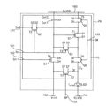
도 2는 본 발명의 일 실시예에 따른 유기 발광 표시 장치의 화소에 인가되는 신호들을 나타내는 타이밍도이다.
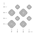
도 3은 본 발명의 일 실시예에 따른 유기 발광 표시 장치의 복수의 화소들을 나타내는 개략적인 평면도이다.
도 4는 본 발명의 일 실시예에 따른 유기 발광 표시 장치의 화소를 나타내는 구체적인 평면도이다.
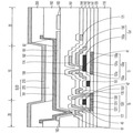
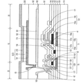
도 5는 도 4의 I-I' 라인을 따라 자른 유기 발광 표시 장치의 일 예를 나타내는 단면도이다.
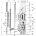
도 6은 도 4의 I-I' 라인을 따라 자른 유기 발광 표시 장치의 다른 예를 나타내는 단면도이다.
도 7은 도 4의 I-I' 라인을 따라 자른 유기 발광 표시 장치의 또 다른 예를 나타내는 단면도이다.
도 8은 본 발명의 다른 실시예에 따른 유기 발광 표시 장치의 화소를 나타내는 구체적인 평면도이다.
도 9는 도 8의 II-II' 라인을 따라 자른 유기 발광 표시 장치의 일 예를 나타내는 단면도이다.
61, 63: 접촉구멍 62: 개구부
110: 기판 151: 스캔선
161: 비아 절연막 162: 평탄화막
171: 데이터선 181: 평탄화 도전 부재
182: 화소 연결 부재 183: 구동 전압선
191: 화소 전극 192: 평탄면
270: 공통 전극 350: 화소 정의막
370: 유기 발광층 PC: 화소 회로
Claims (20)
- 발광 영역 및 비발광 영역을 포함하는 기판;
상기 기판 상에 배치되고, 일부가 상기 발광 영역과 중첩하는 화소 회로;
상기 화소 회로 상에 배치되는 평탄화 도전 부재; 및
상기 평탄화 도전 부재 상에 배치되고, 상기 발광 영역 내에 위치하는 평탄면을 가지는 화소 전극을 포함하는 유기 발광 표시 장치. - 제1항에 있어서, 상기 화소 전극은 상기 평탄화 도전 부재의 직상에 배치되는 것을 특징으로 하는 유기 발광 표시 장치.
- 제1항에 있어서, 상기 평탄화 도전 부재와 동일한 층에 배치되고, 상기 화소 회로와 상기 화소 전극을 서로 연결하는 화소 연결 부재를 더 포함하는 것을 특징으로 하는 유기 발광 표시 장치.
- 제3항에 있어서, 상기 평탄화 도전 부재는 상기 화소 연결 부재와 연결되는 것을 특징으로 하는 유기 발광 표시 장치.
- 제3항에 있어서, 상기 평탄화 도전 부재 상에 배치되는 평탄화막을 더 포함하고,
상기 화소 전극은 상기 평탄화막을 개재하여 상기 평탄화 도전 부재 상에 배치되는 것을 특징으로 하는 유기 발광 표시 장치. - 제5항에 있어서, 상기 평탄화막은 상기 화소 전극과 상기 화소 연결 부재가 접촉하는 접촉 구멍을 포함하고,
상기 접촉 구멍은 상기 비발광 영역에 배치되는 것을 특징으로 하는 유기 발광 표시 장치. - 제5항에 있어서, 상기 평탄화 도전 부재와 동일한 층에 배치되고, 구동 전압을 전달하는 구동 전압선을 더 포함하는 것을 특징으로 하는 유기 발광 표시 장치.
- 제7항에 있어서, 상기 구동 전압선은 상기 비발광 영역에 배치되는 것을 특징으로 하는 유기 발광 표시 장치.
- 제7항에 있어서, 상기 평탄화 도전 부재는 상기 구동 전압선과 연결되는 것을 특징으로 하는 유기 발광 표시 장치.
- 제3항에 있어서, 상기 화소 회로를 덮는 비아 절연막을 더 포함하고,
상기 평탄화 도전 부재는 상기 비아 절연막 상에 배치되는 것을 특징으로 하는 유기 발광 표시 장치. - 제10항에 있어서, 상기 비아 절연막은 상기 화소 연결 부재와 상기 화소 회로가 접촉하는 접촉 구멍을 포함하고,
상기 접촉 구멍은 상기 비발광 영역에 배치되는 것을 특징으로 하는 유기 발광 표시 장치. - 제10항에 있어서, 상기 비아 절연막의 상면의 적어도 일부는 굴곡지고,
상기 평탄화 도전 부재의 상면은 전체적으로 평탄한 것을 특징으로 하는 유기 발광 표시 장치. - 제1항에 있어서, 상기 기판 상에 배치되고, 일부가 상기 발광 영역과 중첩하는 스캔선을 더 포함하고,
상기 평탄화 도전 부재는 상기 스캔선 상에 배치되는 것을 특징으로 하는 유기 발광 표시 장치. - 제13항에 있어서, 상기 기판 상에 배치되고, 일부가 상기 발광 영역과 중첩하며, 상기 스캔선과 교차하는 데이터선을 더 포함하고,
상기 평탄화 도전 부재는 상기 데이터선 상에 배치되는 것을 특징으로 하는 유기 발광 표시 장치. - 제1항에 있어서, 상기 평탄화 도전 부재의 면적은 상기 발광 영역의 면적보다 큰 것을 특징으로 하는 유기 발광 표시 장치.
- 제1항에 있어서,
상기 화소 전극 상에 배치되는 유기 발광층; 및
상기 유기 발광층 상에 배치되어 상기 화소 전극과 마주보는 공통 전극을 더 포함하는 것을 특징으로 하는 유기 발광 표시 장치. - 제16항에 있어서,
상기 화소 회로와 상기 평탄화 도전 부재 사이에 배치되어 상기 화소 회로를 덮는 비아 절연막; 및
상기 비아 절연막 상에 배치되어 상기 평탄화 도전 부재의 적어도 일부를 덮는 평탄화막을 더 포함하는 것을 특징으로 하는 유기 발광 표시 장치. - 제17항에 있어서, 상기 평탄화막은 상기 평탄화 도전 부재의 중심부를 노출시키는 개구부를 포함하고,
상기 화소 전극의 상기 평탄면은 상기 개구부 내에 위치하는 것을 특징으로 하는 유기 발광 표시 장치. - 제17항에 있어서, 상기 평탄화막은 상기 평탄화 도전 부재를 전체적으로 덮고,
상기 화소 전극은 상기 평탄화막을 개재하여 상기 평탄화 도전 부재 상에 배치되는 것을 특징으로 하는 유기 발광 표시 장치. - 제17항에 있어서, 상기 평탄화막 상에 배치되어 상기 화소 전극의 주변부를 덮고, 상기 발광 영역을 정의하는 화소 정의막을 더 포함하는 것을 특징으로 하는 유기 발광 표시 장치.
Priority Applications (2)
| Application Number | Priority Date | Filing Date | Title |
|---|---|---|---|
| KR1020170024953A KR102728403B1 (ko) | 2017-02-24 | 2017-02-24 | 유기 발광 표시 장치 |
| US15/703,786 US10304918B2 (en) | 2017-02-24 | 2017-09-13 | Organic light emitting display device |
Applications Claiming Priority (1)
| Application Number | Priority Date | Filing Date | Title |
|---|---|---|---|
| KR1020170024953A KR102728403B1 (ko) | 2017-02-24 | 2017-02-24 | 유기 발광 표시 장치 |
Publications (2)
| Publication Number | Publication Date |
|---|---|
| KR20180098447A true KR20180098447A (ko) | 2018-09-04 |
| KR102728403B1 KR102728403B1 (ko) | 2024-11-12 |
Family
ID=63246463
Family Applications (1)
| Application Number | Title | Priority Date | Filing Date |
|---|---|---|---|
| KR1020170024953A Active KR102728403B1 (ko) | 2017-02-24 | 2017-02-24 | 유기 발광 표시 장치 |
Country Status (2)
| Country | Link |
|---|---|
| US (1) | US10304918B2 (ko) |
| KR (1) | KR102728403B1 (ko) |
Families Citing this family (16)
| Publication number | Priority date | Publication date | Assignee | Title |
|---|---|---|---|---|
| KR102384774B1 (ko) * | 2017-03-27 | 2022-04-11 | 삼성디스플레이 주식회사 | 유기 발광 표시 장치 |
| KR102487500B1 (ko) * | 2018-01-02 | 2023-01-12 | 삼성디스플레이 주식회사 | 표시 장치 |
| KR102607781B1 (ko) * | 2018-12-28 | 2023-11-28 | 엘지디스플레이 주식회사 | 고 개구율 전계 발광 조명장치 |
| KR102922035B1 (ko) * | 2019-05-16 | 2026-02-03 | 삼성디스플레이 주식회사 | 유기발광표시장치 |
| CN112820763B (zh) | 2019-07-31 | 2024-06-28 | 京东方科技集团股份有限公司 | 电致发光显示面板及显示装置 |
| WO2021018304A1 (zh) | 2019-07-31 | 2021-02-04 | 京东方科技集团股份有限公司 | 显示基板以及显示装置 |
| AU2019279939B2 (en) | 2019-07-31 | 2021-04-08 | Boe Technology Group Co., Ltd. | Display substrate and display device |
| CN110931532B (zh) * | 2019-11-29 | 2022-03-08 | 深圳市华星光电半导体显示技术有限公司 | 一种像素单元、制作方法及显示装置 |
| US12284885B2 (en) * | 2020-03-25 | 2025-04-22 | Chengdu Boe Optoelectronics Technology Co., Ltd. | Display substrate and display device capable of avoiding color cast |
| CN113966551A (zh) | 2020-03-25 | 2022-01-21 | 京东方科技集团股份有限公司 | 显示基板和显示装置 |
| CN113950744B (zh) * | 2020-03-25 | 2024-04-19 | 京东方科技集团股份有限公司 | 显示基板和显示装置 |
| JP2022146602A (ja) * | 2021-03-22 | 2022-10-05 | 株式会社ジャパンディスプレイ | 表示装置 |
| GB2616569A (en) * | 2021-04-28 | 2023-09-13 | Boe Technology Group Co Ltd | Display substrate and display panel |
| CN113223459B (zh) | 2021-04-29 | 2022-09-20 | 京东方科技集团股份有限公司 | 像素电路及其驱动方法、显示基板及显示装置 |
| KR102930759B1 (ko) | 2021-06-25 | 2026-02-25 | 삼성디스플레이 주식회사 | 발광 표시 장치 |
| CN116830184A (zh) * | 2022-01-10 | 2023-09-29 | 京东方科技集团股份有限公司 | 显示基板和显示装置 |
Citations (10)
| Publication number | Priority date | Publication date | Assignee | Title |
|---|---|---|---|---|
| KR20060125634A (ko) * | 2002-03-05 | 2006-12-06 | 산요덴키가부시키가이샤 | 표시 장치 |
| KR20070024778A (ko) * | 2005-08-30 | 2007-03-08 | 삼성에스디아이 주식회사 | 유기 발광표시장치 및 그 제조방법 |
| KR20090003590A (ko) * | 2007-07-03 | 2009-01-12 | 엘지디스플레이 주식회사 | 유기전계발광표시장치 및 그 제조방법 |
| KR20100054351A (ko) * | 2008-11-14 | 2010-05-25 | 삼성전자주식회사 | 유기 발광 표시 장치 및 그 제조 방법 |
| KR20130110987A (ko) * | 2012-03-30 | 2013-10-10 | 엘지디스플레이 주식회사 | 유기발광다이오드 표시장치 및 그 제조방법 |
| KR20140080235A (ko) * | 2012-12-20 | 2014-06-30 | 엘지디스플레이 주식회사 | 플렉서블 유기전계 발광소자 및 그 제조방법 |
| KR20140118010A (ko) * | 2013-03-27 | 2014-10-08 | 삼성디스플레이 주식회사 | 박막 트랜지스터 어레이 기판 및 이를 포함하는 유기 발광 표시 장치 |
| KR20150040668A (ko) * | 2013-10-07 | 2015-04-15 | 삼성디스플레이 주식회사 | 유기 발광 표시 장치 및 유기 발광 표시 장치의 제조 방법 |
| KR20150041509A (ko) * | 2013-10-08 | 2015-04-16 | 엘지디스플레이 주식회사 | 유기 발광 표시 장치 및 그 제조 방법 |
| KR20160080987A (ko) * | 2014-12-30 | 2016-07-08 | 엘지디스플레이 주식회사 | 유기 발광 표시 장치 |
Family Cites Families (4)
| Publication number | Priority date | Publication date | Assignee | Title |
|---|---|---|---|---|
| CN100385475C (zh) * | 2002-12-27 | 2008-04-30 | 株式会社半导体能源研究所 | 显示装置和电子机器 |
| KR101714026B1 (ko) * | 2010-07-02 | 2017-03-09 | 삼성디스플레이 주식회사 | 유기 발광 디스플레이 장치 및 그 제조 방법 |
| KR102407887B1 (ko) | 2014-12-26 | 2022-06-10 | 엘지디스플레이 주식회사 | 유기 발광 디스플레이 장치 및 이의 제조 방법 |
| KR102626961B1 (ko) * | 2016-07-27 | 2024-01-17 | 엘지디스플레이 주식회사 | 하이브리드 타입의 박막 트랜지스터 및 이를 이용한 유기발광 표시장치 |
-
2017
- 2017-02-24 KR KR1020170024953A patent/KR102728403B1/ko active Active
- 2017-09-13 US US15/703,786 patent/US10304918B2/en active Active
Patent Citations (10)
| Publication number | Priority date | Publication date | Assignee | Title |
|---|---|---|---|---|
| KR20060125634A (ko) * | 2002-03-05 | 2006-12-06 | 산요덴키가부시키가이샤 | 표시 장치 |
| KR20070024778A (ko) * | 2005-08-30 | 2007-03-08 | 삼성에스디아이 주식회사 | 유기 발광표시장치 및 그 제조방법 |
| KR20090003590A (ko) * | 2007-07-03 | 2009-01-12 | 엘지디스플레이 주식회사 | 유기전계발광표시장치 및 그 제조방법 |
| KR20100054351A (ko) * | 2008-11-14 | 2010-05-25 | 삼성전자주식회사 | 유기 발광 표시 장치 및 그 제조 방법 |
| KR20130110987A (ko) * | 2012-03-30 | 2013-10-10 | 엘지디스플레이 주식회사 | 유기발광다이오드 표시장치 및 그 제조방법 |
| KR20140080235A (ko) * | 2012-12-20 | 2014-06-30 | 엘지디스플레이 주식회사 | 플렉서블 유기전계 발광소자 및 그 제조방법 |
| KR20140118010A (ko) * | 2013-03-27 | 2014-10-08 | 삼성디스플레이 주식회사 | 박막 트랜지스터 어레이 기판 및 이를 포함하는 유기 발광 표시 장치 |
| KR20150040668A (ko) * | 2013-10-07 | 2015-04-15 | 삼성디스플레이 주식회사 | 유기 발광 표시 장치 및 유기 발광 표시 장치의 제조 방법 |
| KR20150041509A (ko) * | 2013-10-08 | 2015-04-16 | 엘지디스플레이 주식회사 | 유기 발광 표시 장치 및 그 제조 방법 |
| KR20160080987A (ko) * | 2014-12-30 | 2016-07-08 | 엘지디스플레이 주식회사 | 유기 발광 표시 장치 |
Also Published As
| Publication number | Publication date |
|---|---|
| US20180247988A1 (en) | 2018-08-30 |
| US10304918B2 (en) | 2019-05-28 |
| KR102728403B1 (ko) | 2024-11-12 |
Similar Documents
| Publication | Publication Date | Title |
|---|---|---|
| JP7413469B2 (ja) | 薄膜トランジスタアレイ基板、及び表示装置 | |
| KR102728403B1 (ko) | 유기 발광 표시 장치 | |
| KR102392673B1 (ko) | 유기 발광 표시 장치 | |
| KR102614532B1 (ko) | 표시 장치 및 그 제조 방법 | |
| KR102491117B1 (ko) | 유기 발광 표시 장치 | |
| KR102667241B1 (ko) | 유기 발광 표시 장치 | |
| KR102419611B1 (ko) | 유기 발광 표시 장치 | |
| KR102372774B1 (ko) | 유기 발광 표시 장치 | |
| KR102317720B1 (ko) | 유기 발광 표시 장치 및 그 제조 방법 | |
| KR102017764B1 (ko) | 유기 발광 표시 장치 | |
| KR102372775B1 (ko) | 유기 발광 표시 장치 | |
| KR102422108B1 (ko) | 유기 발광 표시 장치 | |
| KR20220099520A (ko) | 유기 발광 표시 장치 | |
| KR102516592B1 (ko) | 유기 발광 표시 장치 | |
| KR102300884B1 (ko) | 유기 발광 표시 장치 | |
| KR102351507B1 (ko) | 유기 발광 표시 장치 | |
| KR102409500B1 (ko) | 유기 발광 표시 장치 | |
| KR102351667B1 (ko) | 유기 발광 표시 장치 | |
| KR102307813B1 (ko) | 유기 발광 표시 장치 | |
| US9190461B2 (en) | Organic light-emitting display device | |
| CN105895026A (zh) | 有机发光二极管显示器 | |
| KR100579549B1 (ko) | 듀얼 플레이트 타입 유기전계 발광소자 및 그 제조방법 | |
| KR20150019698A (ko) | 유기 발광 표시 장치 | |
| CN112750880B (zh) | 有机发光显示设备 | |
| KR101420434B1 (ko) | 유기전계발광표시장치 |
Legal Events
| Date | Code | Title | Description |
|---|---|---|---|
| PA0109 | Patent application |
St.27 status event code: A-0-1-A10-A12-nap-PA0109 |
|
| PG1501 | Laying open of application |
St.27 status event code: A-1-1-Q10-Q12-nap-PG1501 |
|
| R18-X000 | Changes to party contact information recorded |
St.27 status event code: A-3-3-R10-R18-oth-X000 |
|
| P22-X000 | Classification modified |
St.27 status event code: A-2-2-P10-P22-nap-X000 |
|
| A201 | Request for examination | ||
| PA0201 | Request for examination |
St.27 status event code: A-1-2-D10-D11-exm-PA0201 |
|
| P22-X000 | Classification modified |
St.27 status event code: A-2-2-P10-P22-nap-X000 |
|
| P22-X000 | Classification modified |
St.27 status event code: A-2-2-P10-P22-nap-X000 |
|
| P22-X000 | Classification modified |
St.27 status event code: A-2-2-P10-P22-nap-X000 |
|
| E902 | Notification of reason for refusal | ||
| PE0902 | Notice of grounds for rejection |
St.27 status event code: A-1-2-D10-D21-exm-PE0902 |
|
| E13-X000 | Pre-grant limitation requested |
St.27 status event code: A-2-3-E10-E13-lim-X000 |
|
| P11-X000 | Amendment of application requested |
St.27 status event code: A-2-2-P10-P11-nap-X000 |
|
| P13-X000 | Application amended |
St.27 status event code: A-2-2-P10-P13-nap-X000 |
|
| P22-X000 | Classification modified |
St.27 status event code: A-2-2-P10-P22-nap-X000 |
|
| E701 | Decision to grant or registration of patent right | ||
| PE0701 | Decision of registration |
St.27 status event code: A-1-2-D10-D22-exm-PE0701 |
|
| GRNT | Written decision to grant | ||
| PR0701 | Registration of establishment |
St.27 status event code: A-2-4-F10-F11-exm-PR0701 |
|
| PR1002 | Payment of registration fee |
St.27 status event code: A-2-2-U10-U11-oth-PR1002 Fee payment year number: 1 |
|
| PG1601 | Publication of registration |
St.27 status event code: A-4-4-Q10-Q13-nap-PG1601 |
|
| P22-X000 | Classification modified |
St.27 status event code: A-4-4-P10-P22-nap-X000 |