KR20180098148A - Power supply circuit for memory, control apparatus, and power supply method for memory - Google Patents
Power supply circuit for memory, control apparatus, and power supply method for memory Download PDFInfo
- Publication number
- KR20180098148A KR20180098148A KR1020180020647A KR20180020647A KR20180098148A KR 20180098148 A KR20180098148 A KR 20180098148A KR 1020180020647 A KR1020180020647 A KR 1020180020647A KR 20180020647 A KR20180020647 A KR 20180020647A KR 20180098148 A KR20180098148 A KR 20180098148A
- Authority
- KR
- South Korea
- Prior art keywords
- power supply
- memory
- voltage
- supply
- capacitor
- Prior art date
- Legal status (The legal status is an assumption and is not a legal conclusion. Google has not performed a legal analysis and makes no representation as to the accuracy of the status listed.)
- Granted
Links
Images


Classifications
-
- G—PHYSICS
- G11—INFORMATION STORAGE
- G11C—STATIC STORES
- G11C5/00—Details of stores covered by group G11C11/00
- G11C5/14—Power supply arrangements, e.g. power down, chip selection or deselection, layout of wirings or power grids, or multiple supply levels
- G11C5/147—Voltage reference generators, voltage or current regulators; Internally lowered supply levels; Compensation for voltage drops
-
- G—PHYSICS
- G11—INFORMATION STORAGE
- G11C—STATIC STORES
- G11C16/00—Erasable programmable read-only memories
- G11C16/02—Erasable programmable read-only memories electrically programmable
- G11C16/06—Auxiliary circuits, e.g. for writing into memory
- G11C16/30—Power supply circuits
-
- G—PHYSICS
- G11—INFORMATION STORAGE
- G11C—STATIC STORES
- G11C5/00—Details of stores covered by group G11C11/00
- G11C5/14—Power supply arrangements, e.g. power down, chip selection or deselection, layout of wirings or power grids, or multiple supply levels
- G11C5/145—Applications of charge pumps; Boosted voltage circuits; Clamp circuits therefor
-
- G—PHYSICS
- G11—INFORMATION STORAGE
- G11C—STATIC STORES
- G11C5/00—Details of stores covered by group G11C11/00
- G11C5/14—Power supply arrangements, e.g. power down, chip selection or deselection, layout of wirings or power grids, or multiple supply levels
- G11C5/148—Details of power up or power down circuits, standby circuits or recovery circuits
Landscapes
- Engineering & Computer Science (AREA)
- Power Engineering (AREA)
- Power Sources (AREA)
- Read Only Memory (AREA)
- Techniques For Improving Reliability Of Storages (AREA)
Abstract
동작 전원의 공급 재개 시에 불휘발성 메모리용의 콘덴서(커패시터)로 흐르는 돌입 전류를 억제하고, 메모리 전원의 전압 상승 시간을 짧게 한다.
메모리 전원 생성부(12)는, 동작 전원의 공급 개시 시에 미리 정해진 비율로 출력 전압을 상승시킴으로써, 콘덴서(15)에 대하여 메모리 전원을 서서히 공급하고, 역류 방지부(14)가 동작 전원(Pw)의 전압(Vw)이 콘덴서(15)의 충전 전압(Vc)을 하회한 경우에는, 콘덴서(15)로부터 메모리 전원 생성부(12)로 흐르는 역류 전류를 방지하며, 공급 제어부(17)는, Vc가 Vcon 이상인 경우에 불휘발성 메모리(ROM)에 대하여 메모리 전원을 공급하고, Vc가 Vcoff 이하인 경우에 ROM에 대한 메모리 전원의 공급을 정지한다. The inrush current flowing to the capacitor (capacitor) for the nonvolatile memory is suppressed at the time of resumption of the operation power supply, and the voltage rise time of the memory power supply is shortened.
The memory power supply generating section 12 gradually increases the output voltage at a predetermined ratio at the start of supply of the operating power supply so that the memory power supply is gradually supplied to the capacitor 15 and the backflow prevention section 14 supplies the operating power Pw Current supply from the capacitor 15 to the memory power generation section 12 when the voltage Vw of the capacitor 15 is lower than the charging voltage Vc of the capacitor 15. The supply control section 17, The memory power is supplied to the nonvolatile memory (ROM) when Vc is equal to or higher than Vcon, and the supply of the memory power to the ROM is stopped when Vc is equal to or lower than Vcoff.

Description
본 발명은, 데이터 보존용의 불휘발성 메모리에 전원을 공급하기 위한 전원 공급 기술에 관한 것이다. The present invention relates to a power supply technique for supplying power to a nonvolatile memory for data retention.
산업용의 컨트롤러나 필드 기기 등의 하위 기기를 제어하는 서버 장치나 상위 컨트롤러 등의 제어 장치에서는, 제어 대상이 되는 하위 기기의 제어, 감시, 관리 등의 각종 처리에 이용하는 각종 데이터를, SD 카드 등의 불휘발성 메모리에 보존하는 기능을 갖고 있는 것이 있다. 이러한 제어 장치에서는, 불휘발성 메모리로의 데이터 기록 시에 동작 전원이 저하된 경우, 데이터의 결손이나 포맷의 파손이 발생할 가능성이 있다. In a control device such as a server device or an upper controller for controlling a sub-device such as an industrial controller or a field device, various data used for various processes such as control, monitoring, and management of the sub- And has a function of storing the data in a nonvolatile memory. In such a control device, there is a possibility that the data is lost or the format is damaged if the operating power is reduced at the time of recording data into the nonvolatile memory.
종래, 이러한 데이터 보존 기술로서, 동작 전원이 공급되어 있는 통상 동작 시에, 불휘발성 메모리에 공급하고 있는 메모리 전원을 콘덴서(커패시터)에 백업해 두고, 동작 전원이 저하된 경우에는, 불휘발성 메모리에서 실행 중인 기록 동작이 완료하기까지의 기간분의 메모리 전원을, 콘덴서로부터 불휘발성 메모리에 대하여 공급하는 기술이 제안되어 있다(예컨대, 특허문헌 1 등 참조). BACKGROUND ART [0002] Conventionally, as such a data preservation technique, memory power supplied to a nonvolatile memory is backed up in a capacitor (capacitor) during normal operation in which the operating power is supplied, and when the operating power is lowered, A technique has been proposed in which a memory power supply for a period of time until a write operation in execution is completed is supplied from a capacitor to a nonvolatile memory (see, for example, Patent Document 1).
이러한 종래 기술에서는, 불휘발성 메모리에 있어서의 기억 용량의 증대에 따라서, 메모리 전원의 소비량도 증대하기 때문에, 동작 전원의 저하 시에, 불휘발성 메모리에서 실행 중인 기록 동작이 완료할 때까지 기간분의 동작을 보증하기 위해서는, 콘덴서의 대용량화가 필요해진다. 그러나, 동작 전원의 공급이 재개되어 메모리 전원이 콘덴서에 충전될 때, 콘덴서의 대용량화에 수반하여 동작 전원으로부터 콘덴서로 흐르는 돌입 전류가 증대하고, 동작 전원을 공급하는 전원 회로에 악영향을 미치게 하는 경우나, 메모리 전원의 전압 상승이 지연되어 불휘발성 메모리가 동작하지 않는 경우가 있다는 문제점이 있었다. In this conventional technique, the consumption amount of the memory power source is also increased in accordance with the increase in the storage capacity in the nonvolatile memory. Therefore, when the operating power is lowered, In order to guarantee operation, it is necessary to increase the capacity of the capacitor. However, when supply of operating power is resumed and the memory power source is charged in the capacitor, the rush current flowing from the operating power source to the capacitor increases with the capacity increase of the capacitor and adversely affects the power source circuit that supplies the operating power source , There is a problem that the voltage rise of the memory power supply is delayed and the nonvolatile memory does not operate.
본 발명은 이러한 과제를 해결하기 위한 것으로, 동작 전원의 공급 재개 시에, 불휘발성 메모리의 메모리 전원을 백업하기 위한 콘덴서(커패시터)로 흐르는 돌입 전류를 억제할 수 있음과 함께, 메모리 전원의 전압 상승 시간을 단축할 수 있는 전원 공급 기술을 제공하는 것을 목적으로 하고 있다. SUMMARY OF THE INVENTION The present invention has been made in order to solve such a problem, and it is an object of the present invention to provide a nonvolatile memory which can suppress an inrush current flowing to a capacitor (capacitor) for backing up memory power of a nonvolatile memory, And it is an object of the present invention to provide a power supply technology capable of shortening the time.
이러한 목적을 달성하기 위해서, 본 발명에 따른 메모리 전원 공급 회로는, 전원 회로로부터 공급된 동작 전원에 기초하여, 불휘발성 메모리의 동작에 이용하는 메모리 전원을 생성하는 메모리 전원 생성부와, 상기 메모리 전원 생성부에서 생성된 상기 메모리 전원을 백업하는 콘덴서와, 상기 불휘발성 메모리에 대한 상기 메모리 전원의 공급/정지를 제어하는 공급 제어부와, 상기 메모리 전원 생성부와 상기 콘덴서 사이에 접속되어, 상기 동작 전원의 전압이 상기 콘덴서의 충전 전압을 상회한 경우에는, 상기 메모리 전원 생성부의 출력 전압을 상기 콘덴서에 공급하고, 상기 동작 전원의 전압이 상기 충전 전압을 하회한 경우에는, 상기 콘덴서로부터 상기 메모리 전원 생성부로 흐르는 역류 전류를 방지하는 역류 방지부를 구비하며, 상기 메모리 전원 생성부는, 상기 동작 전원의 공급 개시 시에 미리 정해진 비율로 상기 출력 전압을 상승시킴으로써, 상기 콘덴서에 대하여 상기 메모리 전원을 서서히 공급하고, 상기 공급 제어부는, 상기 충전 전압이 제1 전압 이상인 경우에, 상기 불휘발성 메모리에 대하여 상기 메모리 전원을 공급하고, 상기 충전 전압이 제2 전압 이하인 경우에, 상기 불휘발성 메모리에 대한 상기 메모리 전원의 공급을 정지하도록 한 것이다.In order to achieve the above object, a memory power supply circuit according to the present invention includes: a memory power supply generation unit that generates a memory power supply used for operation of a nonvolatile memory, based on operation power supplied from a power supply circuit; A supply controller for controlling supply / stop of the memory power supply to the nonvolatile memory; and a controller connected between the memory power supply generator and the capacitor, And supplies the output voltage of the memory power generation unit to the capacitor when the voltage exceeds the charging voltage of the capacitor, and when the voltage of the operating power supply is lower than the charging voltage, And a reverse flow prevention unit for preventing a reverse flow current flowing through the memory, The generation section gradually supplies the memory power to the capacitor by raising the output voltage at a predetermined ratio at the start of supply of the operating power supply, and the supply control section, when the charging voltage is equal to or higher than the first voltage, The memory power supply is supplied to the nonvolatile memory and the supply of the memory power to the nonvolatile memory is stopped when the charging voltage is equal to or lower than the second voltage.
또한, 본 발명에 따른 상기 메모리 전원 공급 회로의 일 구성예는, 상기 역류 방지부 대신에, 상기 전원 회로와 상기 메모리 전원 생성부 사이에 접속되어, 상기 동작 전원의 전압이 상기 충전 전압을 상회한 경우에는, 상기 동작 전원을 상기 메모리 전원 생성부에 공급하고, 상기 동작 전원의 전압이 상기 충전 전압을 하회한 경우에는, 상기 콘덴서로부터 상기 메모리 전원 생성부를 개재하여 상기 전원 회로로 흐르는 역류 전류를 방지하는 역류 방지부를 구비하는 것이다. Further, one example of the memory power supply circuit according to the present invention is characterized in that, instead of the backflow prevention portion, the memory power supply circuit is connected between the power supply circuit and the memory power supply generation portion, and the voltage of the operation power supply is higher than the charging voltage , The control circuit supplies the operating power to the memory power source generating section, and when the voltage of the operating power source is lower than the charging voltage, a reverse current flowing from the capacitor to the power source circuit through the memory power source generating section is prevented And a backflow prevention part for preventing backflow.
또한, 본 발명에 따른 상기 메모리 전원 공급 회로의 일 구성예는, 상기 메모리 전원 생성부가 상기 전원 회로의 전압이 제3 전압 이상이 된 경우에, 상기 출력 전압의 출력을 개시하도록 한 것이다. Further, an example of the memory power supply circuit according to the present invention is such that when the voltage of the power supply circuit becomes equal to or higher than the third voltage, the output of the output voltage is started.
또한, 본 발명에 따른 제어 장치는, 제어에 이용하는 각종 데이터를 불휘발성 메모리에서 보존하는 제어 장치로서, 상기 불휘발성 메모리에 대하여 메모리 전원을 공급하는 회로로서, 전술한 어느 하나의 메모리 전원 공급 회로를 구비하고 있다. The control device according to the present invention is a control device for saving various kinds of data used for control in a nonvolatile memory, which is a circuit for supplying memory power to the nonvolatile memory, Respectively.
또한, 본 발명에 따른 상기 제어 장치의 일 구성예는, 상기 동작 전원의 생성에 이용되는 주전원의 주전원 전압이 제4 전압을 하회한 경우, 상기 주전원의 차단을 예고하는 주전원 저하 출력을 출력하는 전원 차단 예고부와, 상기 동작 전원의 전압이 제5 전압의 저하를 하회한 경우, 상기 동작 전원의 전압 저하를 나타내는 동작 전원 저하 출력을 출력하는 전원 전압 검출부와, 상기 주전원 저하 출력이 상기 주전원의 차단을 예고하고 있음과 함께, 상기 동작 전원 저하 출력이 상기 동작 전원의 전압 저하를 나타내고 있지 않은 경우, 상기 동작 전원의 전원 공급 상태가 전원 저하 상태에 있다고 판정하는 전원 상태 판정부와, 상기 주전원 저하 출력에 의해 상기 주전원의 차단이 예고된 경우, 상기 불휘발성 메모리에서 기록해야 할 데이터의 유무를 확인하고, 얻어진 확인 결과에 기초하여, 상기 메모리 전원에 관한 강제 차단의 필요와 불필요를 나타내는 강제 차단 제어 출력을 출력하는 연산 제어 회로와, 상기 전원 상태 판정부에 의해 상기 동작 전원이 상기 전원 저하 상태에 있다고 판정되어 있는 기간에 있어서, 상기 연산 제어 회로로부터 출력된 새로운 강제 차단 제어 출력을 받아들여, 상기 공급 제어부로 유지 출력하는 강제 차단 유지부를 더욱 구비하고, 상기 공급 제어부는, 상기 강제 차단 유지부로부터의 유지 출력이 강제 차단 필요를 나타내는 경우, 상기 불휘발성 메모리에 대한 상기 메모리 전원의 공급을 강제적으로 차단하도록 한 것이다. According to another aspect of the present invention, there is provided a control apparatus for a vehicle, comprising: a power source for outputting a main power source lowering output for predicting shutdown of the main power source when the main power source voltage of the main power source used for generating the operating power source is lower than a fourth voltage; A power supply voltage detector for outputting an operating power supply lowering output indicating a voltage drop of the operating power supply when the voltage of the operating power supply is lower than the fifth voltage; A power supply state determining unit that determines that the power supply state of the operating power supply is in a power supply lowering state when the operating power supply lowering output does not indicate a voltage drop of the operating power supply, The presence or absence of data to be recorded in the nonvolatile memory is determined And an operation control circuit for outputting, based on the obtained confirmation result, a forced cutoff control output indicating necessity and necessity of forcible cutoff relating to the memory power supply, Further comprising a forced shut-off holding section for receiving a new forced shut-off control output from the arithmetic control circuit and maintaining the output of the forced cut-off control output in the supply control section during a period determined to be the supply shut-off control section The supply of the memory power to the nonvolatile memory is forcibly interrupted.
또한, 본 발명에 따른 상기 제어 장치의 일 구성예는, 상기 전원 차단 예고부가, 상기 주전원의 복구에 따라서 상기 주전원 전압이 제6 전압 이상으로 상승한 경우, 상기 주전원 저하 출력의 출력을 정지하고, 상기 전원 상태 판정부는, 상기 주전원 저하 출력의 출력이 정지하고 있음과 함께, 상기 동작 전원 저하 출력이 상기 동작 전원의 전압 저하를 나타내고 있지 않은 경우, 상기 동작 전원의 전원 공급 상태가 전원 공급 상태에 있다고 판정하고, 상기 강제 차단 유지부는, 상기 전원 상태 판정부에서의 판정 결과가 상기 전원 저하 상태로부터 상기 전원 공급 상태로 변화한 경우, 강제 차단 불필요를 상기 공급 제어부로 유지 출력하며, 상기 공급 제어부는, 상기 강제 차단 유지부로부터의 유지 출력이 강제 차단 불필요를 나타내는 경우, 상기 불휘발성 메모리에 대한 상기 메모리 전원의 강제 차단을 해제하도록 한 것이다. According to an embodiment of the control apparatus according to the present invention, the power shut-off prevention unit may stop the output of the main power source lowering output when the main power source voltage rises above the sixth voltage in accordance with the recovery of the main power source, The power supply state judging section judges that the power supply state of the operating power supply is in the power supply state when the output of the main power supply lowering output is stopped and the operating power supply lowering output does not indicate the voltage drop of the operating power supply And the forced shut-off maintaining unit maintains the forced shut-off state to the supply control unit when the determination result in the power state determining unit changes from the power-down state to the power supply state, and the supply control unit When the holding output from the forced blocking holding portion indicates that the forced blocking is not required, To a force to release the blocking of the memory power supply for the memory.
또한, 본 발명에 따른 메모리 전원 공급 방법은, 메모리 전원 생성부가, 전원 회로로부터 공급된 동작 전원에 기초하여, 불휘발성 메모리의 동작에 이용하는 메모리 전원을 생성하는 메모리 전원 생성 단계와, 콘덴서가, 상기 메모리 전원 생성부에서 생성된 상기 메모리 전원을 백업하는 단계와, 공급 제어부가, 상기 불휘발성 메모리에 대한 상기 메모리 전원의 공급/정지를 제어하는 공급 제어 단계와, 상기 메모리 전원 생성부와 상기 콘덴서 사이에 접속된 역류 방지부가, 상기 동작 전원의 전압이 상기 콘덴서의 충전 전압을 상회한 경우에는, 상기 메모리 전원 생성부의 출력 전압을 상기 콘덴서에 공급하고, 상기 동작 전원의 전압이 상기 충전 전압을 하회한 경우에는, 상기 콘덴서로부터 상기 메모리 전원 생성부로 흐르는 역류 전류를 방지하는 역류 방지 단계를 구비하고, 상기 메모리 전원 생성 단계는, 상기 동작 전원의 공급 개시 시에 미리 정해진 비율로 상기 출력 전압을 상승시킴으로써, 상기 콘덴서에 대하여 상기 메모리 전원을 서서히 공급하고, 상기 공급 제어 단계는, 상기 충전 전압이 제1 전압 이상인 경우에, 상기 불휘발성 메모리에 대하여 상기 메모리 전원을 공급하고, 상기 충전 전압이 제2 전압 이하인 경우에, 상기 불휘발성 메모리에 대한 상기 메모리 전원의 공급을 정지하도록 한 것이다. According to another aspect of the present invention, there is provided a memory power supply method including: a memory power supply generation step of generating a memory power supply used for operation of a nonvolatile memory based on operation power supplied from a power supply circuit; A supply control step of controlling supply / stop of the memory power supply to the nonvolatile memory; and a supply control step of supplying / stopping the memory power supply to the nonvolatile memory, When the voltage of the operating power supply exceeds the charging voltage of the capacitor, supplies the output voltage of the memory power generating unit to the capacitor, and when the voltage of the operating power supply is lower than the charging voltage A capacitor for preventing a reverse current flowing from the capacitor to the memory power source generator, Wherein the memory power generation step gradually supplies the memory power to the capacitor by raising the output voltage at a predetermined ratio at the start of supply of the operating power supply, And supplies the memory power supply to the nonvolatile memory when the charging voltage is equal to or higher than the first voltage and stops supplying the memory power to the nonvolatile memory when the charging voltage is equal to or lower than the second voltage It is.
또한, 본 발명에 따른 상기 메모리 전원 공급 방법의 일 구성예는, 상기 역류 방지 단계 대신에, 상기 전원 회로와 상기 메모리 전원 생성부 사이에 접속된 상기 역류 방지부가, 상기 동작 전원의 전압이 상기 충전 전압을 상회한 경우에는, 상기 동작 전원을 상기 메모리 전원 생성부에 공급하고, 상기 동작 전원의 전압이 상기 충전 전압을 하회한 경우에는, 상기 콘덴서로부터 상기 메모리 전원 생성부를 개재하여 상기 전원 회로로 흐르는 역류 전류를 방지하는 역류 방지 단계를 구비하는 것이다. According to an embodiment of the memory power supply method according to the present invention, the backflow prevention unit connected between the power supply circuit and the memory power supply generation unit may be configured such that the voltage of the operation power supply is higher than the charging Supply voltage from the capacitor to the power supply circuit through the memory power supply generator when the voltage of the operating power supply is lower than the charging voltage, And a backflow prevention step for preventing a backflow current.
본 발명에 따르면, 동작 전원 공급 개시 시에는, 콘덴서에 공급되는 출력 전압의 상승하는 기울기가, 메모리 전원 생성부에 의해 억제되기 때문에, 콘덴서로의 돌입 전류가 억제됨과 함께, 콘덴서의 충전 전압이 불휘발성 메모리의 동작 개시 전압 이상에 달한 시점으로부터 불휘발성 메모리로의 메모리 전원의 공급이 개시된다. 따라서, 불휘발성 메모리의 기억 용량 증대에 따라서 콘덴서를 대용량화해도, 동작 전원으로부터 콘덴서로 흐르는 돌입 전류를 억제할 수 있고, 동작 전원을 공급하는 전원 회로에 대한 악영향을 회피할 수 있음과 함께, 불휘발성 메모리에 공급되는 메모리 전원의 전압 상승 시간을 단축하는 것이 가능해진다. According to the present invention, at the start of the operation power supply, the rising slope of the output voltage supplied to the condenser is suppressed by the memory power generator, so that the inrush current to the condenser is suppressed, The supply of the memory power to the nonvolatile memory starts from the time point when the voltage reaches the operation starting voltage of the volatile memory. Therefore, even if the capacity of the capacitor is increased in accordance with the increase of the storage capacity of the nonvolatile memory, an inrush current flowing from the operation power supply to the capacitor can be suppressed and adverse effects on the power supply circuit for supplying operation power can be avoided, It is possible to shorten the voltage rise time of the memory power supply supplied to the memory.
도 1은 제1 실시의 형태에 따른 제어 장치의 구성을 나타내는 블럭도이다.
도 2는 동작 전원 공급 개시 시에 있어서의 회로 전압의 변화를 나타내는 그래프이다.
도 3은 동작 전원 공급 정지 시에서의 회로 전압의 변화를 나타내는 그래프이다.
도 4는 동작 전원 공급 재개 시에서의 회로 전압의 변화를 나타내는 그래프이다.
도 5는 제2 실시의 형태에 따른 제어 장치의 구성을 나타내는 블럭도이다.
도 6은 전원 상태 판정 시에서의 회로 전압의 변화를 나타내는 타이밍 차트이다.
도 7은 제2 실시의 형태에 따른 전원 상태 판정 시에서의 회로 전압의 변화를 나타내는 그래프이다.
도 8은 제3 실시의 형태에 따른 전원 상태 판정 시에서의 회로 전압의 변화를 나타내는 그래프이다. 1 is a block diagram showing a configuration of a control apparatus according to the first embodiment.
2 is a graph showing a change in circuit voltage at the start of operation power supply.
3 is a graph showing changes in circuit voltage at the time of stopping the operation power supply.
4 is a graph showing changes in the circuit voltage at the time of restarting the operation power supply.
5 is a block diagram showing a configuration of a control apparatus according to the second embodiment.
6 is a timing chart showing a change in the circuit voltage at the time of the power supply state determination.
7 is a graph showing a change in the circuit voltage at the time of the power supply state determination according to the second embodiment.
8 is a graph showing a change in the circuit voltage in the power supply state determination according to the third embodiment.
다음으로, 본 발명의 실시의 형태에 관해서 도면을 참조하여 설명한다. Next, embodiments of the present invention will be described with reference to the drawings.
[제1 실시의 형태][First embodiment] Fig.
우선, 도 1을 참조하여, 본 발명의 제1 실시의 형태에 따른 제어 장치(1)에 관해서 설명한다. 도 1은, 제1 실시의 형태에 따른 제어 장치의 구성을 나타내는 블럭도이다. First, a
이 제어 장치(1)는, 예컨대 산업용의 컨트롤러나 필드 기기 등의 하위 기기를 제어하는, 서버 장치나 상위 컨트롤러 등의 제어 장치로 이루어지고, 제어 대상이 되는 하위 기기의 제어, 감시, 관리 등의 각종 처리에 이용하는 각종 데이터를 불휘발성 메모리에 보존하는 기능을 갖고 있다. This
도 1에 나타낸 바와 같이, 제어 장치(1)에는, 주된 내부 회로로서, 연산 제어 회로(CNT), 불휘발성 메모리(ROM), 전원 회로(SP), 및 메모리 전원 공급 회로(10)가 설치되어 있다. 1, the
연산 제어 회로(CNT)는, CPU나 그 주변 회로를 갖고, 이들 하드웨어와 프로그램이 협동함으로써, 제어 대상이 되는 하위 기기의 제어, 감시, 관리 등의 각종 처리를 행하는 기능과, 이들 처리에 이용하는 각종 데이터를 불휘발성 메모리(ROM)에 보존하는 기능을 갖고 있다. The operation control circuit (CNT) has a CPU and its peripheral circuits. Functions of these hardware and programs cooperate with each other to perform various processes such as control, monitoring, and management of the lower-level devices to be controlled, and various functions And has a function of storing data in a nonvolatile memory (ROM).
불휘발성 메모리(ROM)는, 예컨대 SD 카드 등의 NVRAM(Non-Volatile RAM)로 이루어지고, 메모리 전원 공급 회로(10)로부터 공급된 메모리 전원에 의해, 연산 제어 회로(CNT)로부터의 데이터의 기록 동작이나 독출 동작을 행하는 기능을 갖고 있다. The nonvolatile memory (ROM) is composed of an NVRAM (non-volatile RAM) such as an SD card. The memory power supplied from the memory
전원 회로(SP)는, 일반적인 전원 회로로 이루어지고, 예컨대 상용 AC 전원 등으로 이루어지는 외부로부터의 주전원(Pin)에 기초하여 동작 전원(Pw)을 생성하고, 연산 제어 회로(CNT) 및 메모리 전원 공급 회로(10)를 포함하는 내부 회로의 각각에 공급하는 기능을 갖고 있다. The power supply circuit SP is constituted by a general power supply circuit and generates an operation power Pw based on an external main power Pin made of a commercially available AC power supply or the like and supplies an operation control circuit CNT and a memory power supply To the respective internal circuits including the circuit (10).
[메모리 전원 공급 회로][Memory power supply circuit]
메모리 전원 공급 회로(10)는, 전원 회로(SP)의 동작 전원(Pw)에 기초하여, 불휘발성 메모리(ROM)에서 이용하는 메모리 전원(Pm)을 생성하여 출력하는 기능을 갖고 있고, 주된 회로부로서, 전원 감시부(11), 메모리 전원 생성부(12), 전압 비교부(13), 역류 방지부(14), 콘덴서(15), 전압 감시부(16), 및 공급 제어부(17)가 설치되어 있다. The memory
전원 감시부(11)는, 동작 전원(Pw)의 공급 개시 시에 동작 전원(Pw)의 동작 전원 전압(Vw)이 미리 설정한 출력 개시 전압(Vmon)(제3 전압) 이상으로 상승한 경우에, 메모리 전원 생성부(12)에 대하여 메모리 전원(Pm)의 출력 개시를 지시하는 기능을 갖고 있다. 이하에서는, 메모리 전원(Pm)이, 메모리 전원 생성부(12)로부터 역류 방지부(14), 콘덴서(15), 공급 제어부(17)로 거쳐 불휘발성 메모리(ROM)에 대하여 공급되는 일련의 전원 계통을 가리키는 것으로 한다. 또, 편의상, 메모리 전원(Pm) 중, 콘덴서(15)에서 백업되는 메모리 전원을 Pc라고 부르고, 공급 제어부(17)로부터 불휘발성 메모리(ROM)에 대하여 공급되는 메모리 전원을 Prom라고 부르는 일도 있다. When the operating power supply voltage Vw of the operating power Pw rises above the preset output start voltage Vmon (third voltage) at the start of supply of the operating power Pw , And has a function of instructing the memory power
메모리 전원 생성부(12)는, 전원 회로(SP)로부터 공급된 동작 전원(Pw)에 기초하여, 불휘발성 메모리(ROM)의 동작에 이용하는 메모리 전원(Pm)을 생성하는 기능과, 동작 전원(Pw)의 공급 개시 시에는, 전원 감시부(11)로부터의 출력 개시의 지시에 따라서, 미리 정해진 비율로 메모리 전원(Pm)의 출력 전압(Vm)을 상승시킴으로써, 콘덴서(15)에 대하여 메모리 전원(Pm)을 서서히 공급하는 기능을 갖고 있다. The memory power
전압 비교부(13)는, 메모리 전원(Pm)(Pc)의 메모리 전원 전압, 즉 콘덴서(15)의 충전 전압(Vc)과 동작 전원(Pw)의 동작 전원 전압(Vw)을 비교하는 기능을 갖고 있다. The
역류 방지부(14)는, 메모리 전원 생성부(12)와 콘덴서(15) 사이에 접속되어, 전압 비교부(13)에 의해 동작 전원(Pw)의 동작 전원 전압(Vw)이 콘덴서(15)의 충전 전압(Vc)을 상회한 것이 검출된 경우에는, 메모리 전원 생성부(12)로부터의 출력 전압(Vm)을 콘덴서(15)에 공급하는 기능과, 전압 비교부(13)에 의해 동작 전원 전압(Vw)이 충전 전압(Vc)을 하회한 것이 검출된 경우에는, 콘덴서(15)로부터 역류 방지부(14)로 흐르는 역류 전류를 방지하는 기능을 갖고 있다. The
또, 본 실시의 형태에서는, 도 1에 나타낸 바와 같이, 역류 방지부(14)가 메모리 전원 생성부(12)와 콘덴서(15) 사이에 접속되어 있는 경우를 예로 설명하지만, 이것에 한정되는 것은 아니다. 예컨대, 메모리 전원 생성부(12)와 전원 회로(SP) 사이에 역류 방지부(14)를 접속해도 좋다. 이 경우, 역류 방지부(14)는, 전압 비교부(13)에 의해 Vw가 Vc를 상회한 것이 검출된 경우에는, 동작 전원(Pw)을 메모리 전원 생성부(12)에 공급하고, Vw가 Vc를 하회한 것이 검출된 경우에는, 콘덴서(15)로부터 메모리 전원 생성부(12)를 개재하여 전원 회로(SP)로 흐르는 역류 전류를 방지하는 것이 된다. 이러한 구성이라도, 도 1의 경우와 동일한 작용 효과를 얻을 수 있다. 1, the
콘덴서(15)는, 전원 백업용의 일반적인 콘덴서나 커패시터로 이루어지고, 역류 방지부(14)를 개재하여 메모리 전원 생성부(12)로부터 공급된 출력 전압(Vm)을 항상 충전함으로써, 불휘발성 메모리(ROM)에서 이용하는 메모리 전원(Pm)을(메모리 전원(Pc)으로서) 백업하는 기능을 갖고 있다. The
전압 감시부(16)는, 콘덴서(15)의 충전 전압(Vc)을 감시하고, Vc가 미리 설정한, 불휘발성 메모리(ROM)의 동작 개시 전압(제1 전압) 이상의 전압을 나타내는, 공급 개시 전압(Vcon) 이상으로 상승한 경우에, 불휘발성 메모리(ROM)에 대한 메모리 전원(Pm)(Pc→Prom)의 공급을 지시하는 기능과, Vc가 미리 설정한 공급 정지 전압(Vcoff)(제2 전압) 이하로 저하된 경우에, 불휘발성 메모리(ROM)에 대한 메모리 전원(Pm)(Pc→Prom)의 공급 정지를 지시하는 기능을 갖고 있다. The
공급 제어부(17)는, 콘덴서(15)와 불휘발성 메모리(ROM) 사이에 설치되어, 전압 감시부(16)로부터의 공급 지시에 따라서, 메모리 전원(Pm)을 불휘발성 메모리(ROM)로 공급하는(Pc→Prom) 기능과, 전압 감시부(16)로부터의 공급 정지 지시에 따라서, 불휘발성 메모리(ROM)에 대한 메모리 전원(Pm)의 공급(Pc→Prom)을 정지하는 기능을 갖고 있다. The
[동작 전원 공급 개시 시의 회로 동작][Circuit operation at the start of operation power supply]
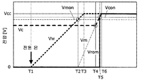
다음으로, 도 2를 참조하여, 본 실시의 형태에 따른 제어 장치(1)에 있어서의, 동작 전원 공급 개시 시의 회로 동작에 관해서 설명한다. 도 2는, 동작 전원 공급 개시 시에 있어서의 회로 전압의 변화를 나타내는 그래프이다. Next, with reference to Fig. 2, the circuit operation at the start of operation power supply in the
우선, 시각 T1에 있어서, 제어 장치(1)에 대하여 주전원(Pin)의 공급이 개시된 경우, 동작 전원(Pw)의 동작 전원 전압(Vw)이 서서히 상승한다. 이 때, 동작 전원 전압(Vw)은 충분히 상승하고 있지 않기 때문에, 메모리 전원 생성부(12)로부터 출력 전압(Vm)은 출력되고 있지 않고, 콘덴서(15)의 충전 전압(Vc)은 0 V이다. First, when supply of the main power Pin to the
그 후, 시각 T2에 있어서, 동작 전원 전압(Vw)이 출력 개시 전압(Vmon)까지 상승한 시점에서, 전원 감시부(11)로부터 출력 개시가 지시되어, 메모리 전원 생성부(12)로부터 미리 정해진 비율로 규정 전원 전압 Vcc까지 상승하는 출력 전압(Vm)이 출력된다. 이 때, 전압 비교부(13)에 의해, Vw가 충전 전압(Vc)보다 높은 것이 검출되고 있기 때문에, Vm은 역류 방지부(14)를 개재하여 콘덴서(15)에 공급되어 Vc로서 서서히 충전된다. 이 비율, 즉 단위 시간당의 상승 전압에 관해서는, 콘덴서(15)의 용량, 동작 전원(Pw)의 규정 전원 전압 Vcc, 전원 회로(SP)에서 허용되는 순간 전류 등의 회로 조건에 기초하여, 미리 설정해 두면 좋다. Thereafter, at the time T2, when the operating power supply voltage Vw rises to the output start voltage Vmon, the output start instruction is issued from the power
계속해서 시각 T3에, 동작 전원 전압(Vw)이 규정 전원 전압 Vcc에 도달하여 일정해지고, 그 후의 시각 T4에 있어서, Vc가 공급 개시 전압(Vcon)까지 상승한 시점에서, 전압 감시부(16)로부터 공급 개시가 지시되어, 공급 제어부(17)에 의해, 불휘발성 메모리(ROM)에 대하여 메모리 전원(Pm)의 공급(Pc→Prom)이 개시된다. 이에 따라, 시각 T5에 Vc가 Vcc에 도달하여 일정해짐과 함께, 불휘발성 메모리(ROM)의 ROM 전원 전압(Vrom)도 Vcc에 도달하여 일정해진다. 이 때, 콘덴서(15)에 충분한 전하가 충전되어 있기 때문에, 불휘발성 메모리(ROM)가 동작을 개시하더라도 Vrom은 거의 안정되어 있다. Subsequently, at the time T3, when the operating power source voltage Vw reaches the specified power source voltage Vcc and becomes constant and at the time T4 after that, when the voltage Vc rises to the supply start voltage Vcon, The supply start is instructed and the
이에 따라, 동작 전원 공급 개시 시에는, 콘덴서(15)에 공급되는 출력 전압(Vm)의 상승하는 비율이, 메모리 전원 생성부(12)에 의해 억제되기 때문에, 콘덴서(15)로의 돌입 전류도 억제되게 된다. 따라서, 불휘발성 메모리(ROM)의 기억 용량 증대에 따라서 콘덴서(15)를 대용량화해도, 동작 전원(Pw)으로부터 콘덴서(15)로 흐르는 돌입 전류를 억제할 수 있고, 동작 전원(Pw)을 공급하는 전원 회로(SP)에 대한 악영향을 회피하는 것이 가능해진다. The increase in the output voltage Vm supplied to the
[동작 전원 공급 정지 시의 회로 동작][Circuit operation when operation power supply is stopped]
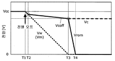
다음으로, 도 3을 참조하여, 본 실시의 형태에 따른 제어 장치(1)에 있어서의, 동작 전원 공급 정지 시의 회로 동작에 관해서 설명한다. 도 3은, 동작 전원 공급 정지 시에서의 회로 전압의 변화를 나타내는 그래프이다. Next, with reference to Fig. 3, the circuit operation at the time of stopping the operation power supply in the
우선, 시각 T1에 있어서, 제어 장치(1)에 대한 주전원(Pin)의 공급이 정지된 경우, 전원 회로(SP)로부터의 동작 전원(Pw)의 동작 전원 전압(Vw)이 서서히 저하된다. 또, 시각 T1 이전에서는, Vw는 규정 전원 전압 Vcc까지 충분히 상승하고 있고, 메모리 전원 생성부(12)로부터 Vcc와 거의 동일한 출력 전압(Vm)이 출력되고 있으며, 콘덴서(15)의 충전 전압(Vc)도 Vcc와 거의 동일한 값을 나타내고 있다. First, at the time T1, when the supply of the main power Pin to the
계속해서, 시각 T2에 있어서, 전압 비교부(13)에 의해, 동작 전원 전압(Vw)이 충전 전압(Vc)보다 저하된 것이 검출된 경우, 역류 방지부(14)에 의해 콘덴서(15)로부터 메모리 전원 생성부(12)로의 역류 전류가 방지된다. 이에 따라, Vw에 따라서 Vc가 저하되기 때문에, 콘덴서(15)에 대한 메모리 전원(Pm)의 공급이 정지되지만, 역류 전류에 의한 Vc의 저하를 회피할 수 있다. 따라서, 메모리 전원 생성부(12)로부터의 Pm의 공급이 정지한 후에도, 일정한 기간에 걸쳐, 콘덴서(15)에 백업되어 있는 Pm을 불휘발성 메모리(ROM)에 공급할 수 있고(Pc→Prom), 불휘발성 메모리(ROM)의 동작을 보증할 수 있다. Subsequently, at the time T2, when the
이 후, 시각 T3에 있어서, Vc가 공급 정지 전압(Vcoff)까지 저하된 시점에서, 전압 감시부(16)로부터 공급 정지가 지시되어, 공급 제어부(17)에 의해, 불휘발성 메모리(ROM)에 대한 Pm의 공급(Pc→Prom)이 정지된다. 이에 따라, 불휘발성 메모리(ROM)의 ROM 전원 전압(Vrom)은 시각 T5에 0 V까지 저하되지만, Vc는 Vcoff와 거의 동일한 전압으로 유지되게 된다. Thereafter, at the time T3, when the voltage Vc has fallen to the supply stop voltage Vcoff, the supply of the supply stoppage is instructed from the
이 때, Vcoff로서 불휘발성 메모리(ROM)의 최저 동작 전압을 이용한 경우, 시각 T2부터 시각 T3까지 불휘발성 메모리(ROM)의 동작이 보증되게 된다. 따라서, 불휘발성 메모리(ROM)에서 소비되는 전력이나 콘덴서(15)의 용량을 적절하게 선택함으로써, 시각 T2부터 시각 T3까지의 기간, 즉 필요해지는 불휘발성 메모리(ROM)의 동작 보증 기간을 얻을 수 있다. At this time, when the lowest operating voltage of the nonvolatile memory (ROM) is used as Vcoff, the operation of the nonvolatile memory (ROM) from time T2 to time T3 is guaranteed. Therefore, by appropriately selecting the power consumed in the nonvolatile memory (ROM) or the capacity of the
[동작 전원 공급 재개 시의 회로 동작][Circuit operation at resumption of operation power supply]
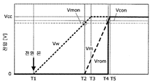
다음으로, 도 4를 참조하여, 본 실시의 형태에 따른 제어 장치(1)에 있어서의, 동작 전원 공급 재개 시의 회로 동작에 관해서 설명한다. 도 4는, 동작 전원 공급 재개 시에서의 회로 전압의 변화를 나타내는 그래프이다. Next, with reference to Fig. 4, the circuit operation at the time of resumption of operation power supply in the
우선, 시각 T1에 있어서, 제어 장치(1)에 대하여 주전원(Pin)의 공급이 재개된 경우, 동작 전원(Pw)의 동작 전원 전압(Vw)이 서서히 상승한다. 이 때, 동작 전원 전압(Vw)은 충분히 상승하고 있지 않기 때문에, 메모리 전원 생성부(12)로부터 출력 전압(Vm)은 출력되고 있지 않지만, 콘덴서(15)에는 직전 동작에 있어서의 충전 전압(Vc)이 유지되고 있다. First, at the time T1, when the supply of the main power Pin to the
그 후, 시각 T2에 있어서, 동작 전원 전압(Vw)이 출력 개시 전압(Vmon)까지 상승한 시점에서, 전원 감시부(11)로부터 출력 개시가 지시되어, 메모리 전원 생성부(12)로부터 미리 정해진 비율로 규정 전원 전압 Vcc까지 상승하는 출력 전압(Vm)이 출력된다. 이 때, 전압 비교부(13)에 의해, Vc가 Vm보다 높은 것이 검출되고 있기 때문에, 콘덴서(15)에 대한 충전은 행해지지 않는다. Thereafter, at the time T2, when the operating power supply voltage Vw rises to the output start voltage Vmon, the output start instruction is issued from the power
계속해서 시각 T3에, 동작 전원 전압(Vw)이 규정 전원 전압 Vcc에 도달하여 일정해지고, 그 후의 시각 T4에 있어서 Vm이 Vc에 도달하여 전압 비교부(13)에 의해, Vc가 Vm보다 낮은 것이 검출된 후, 콘덴서(15)가 서서히 충전되고 Vc가 상승을 개시한다. 이에 따라, 시각 T5에, Vc가 공급 개시 전압(Vcon)까지 상승한 시점에서, 전압 감시부(16)로부터 공급 개시가 지시되어, 공급 제어부(17)에 의해, 불휘발성 메모리(ROM)에 대한 메모리 전원(Pc)의 공급이 개시된다. 그 후, 시각 T6에 Vc가 Vcc에 도달하여 일정해짐과 함께, 불휘발성 메모리(ROM)에서 이용하는 메모리 전원(Pm)(Prom)의 전압(Vrom)도 Vcc에 도달하여 일정해진다. 이 때, 콘덴서(15)에 충분한 전하가 충전되어 있기 때문에, 불휘발성 메모리(ROM)가 동작을 개시하더라도 Vrom은 거의 안정되어 있다. Subsequently, at time T3, when the operating power supply voltage Vw reaches the specified power supply voltage Vcc and becomes constant, and Vm reaches Vc at the subsequent time T4, the
이에 따라, 동작 전원 공급 재개 시에는, 콘덴서(15)에 직전 동작의 충전 전압(Vc)이 유지되어 있고, 출력 전압(Vm)이 Vc에 도달할 때까지 콘덴서(15)에 대한 충전 전류는 흐르지 않기 때문에, 콘덴서(15)로의 돌입 전류도 억제되게 된다. 또한, Vm이 Vc에 도달한 후에 관해서는, 콘덴서(15)에 공급되는 출력 전압(Vm)의 상승하는 비율이, 메모리 전원 생성부(12)에 의해 억제되기 때문에, 콘덴서(15)로의 돌입 전류도 억제되게 된다. 따라서, 불휘발성 메모리(ROM)의 기억 용량 증대에 따라서 콘덴서(15)를 대용량화하더라도, 동작 전원(Pw)으로부터 콘덴서(15)로 흐르는 돌입 전류를 억제할 수 있고, 동작 전원(Pw)을 공급하는 전원 회로(SP)에 대한 악영향을 회피하는 것이 가능해진다. Accordingly, at the time of resumption of the operation power supply, the charging voltage Vc of the immediately preceding operation is held in the
[제1 실시의 형태의 효과][Advantages of First Embodiment]
이와 같이, 본 실시의 형태는, 전원 회로(SP)로부터 공급된 동작 전원(Pw)에 기초하여, 불휘발성 메모리(ROM)에서 이용하는 메모리 전원(Pm)을 생성하는 메모리 전원 생성부(12)와, 메모리 전원 생성부(12)에서 생성된 메모리 전원(Pm)을(Pc로 하여) 백업하는 콘덴서(15)와, 불휘발성 메모리(ROM)에 대한 메모리 전원(Pm)(Pc→Prom)의 공급/정지를 제어하는 공급 제어부(17)를 구비하고, 메모리 전원 생성부(12)가, Pw의 공급 개시 시에 미리 정해진 비율로 출력 전압(Vm)을 상승시킴으로써, 콘덴서(15)에 대하여 메모리 전원(Pm)을 서서히 공급하고, 공급 제어부(17)가, 콘덴서(15)에서 백업되어 있는 불휘발성 메모리(ROM)에 대한 메모리 전원(Pm)(Pc)의 충전 전압(Vc)이 공급 개시 전압(Vcon) 이상인 경우에, 불휘발성 메모리(ROM)에 대하여 메모리 전원(Pc)을 공급하도록 한 것이다. As described above, the present embodiment includes the memory power
이에 따라, 동작 전원 공급 개시 시에는, 콘덴서(15)에 공급되는 출력 전압(Vm)의 상승하는 비율이, 메모리 전원 생성부(12)에 의해 억제되기 때문에, 콘덴서(15)로의 돌입 전류도 억제됨과 함께, 콘덴서(15)의 충전 전압(Vc)이 불휘발성 메모리(ROM)의 동작 개시 전압 이상에 도달한 시점으로부터, 불휘발성 메모리(ROM)로의 메모리 전원(Pm)(Pc→Prom)의 공급이 개시된다. 따라서, 불휘발성 메모리(ROM)의 기억 용량 증대에 따라서 콘덴서(15)를 대용량화하더라도, 동작 전원(Pw)으로부터 콘덴서(15)로 흐르는 돌입 전류를 억제할 수 있고, 동작 전원(Pw)을 공급하는 전원 회로(SP)에 대한 악영향을 회피하는 것이 가능해진다. Accordingly, at the start of the operation power supply, since the rising ratio of the output voltage Vm supplied to the
이에 더하여, 본 실시의 형태는, 메모리 전원 생성부(12)와 콘덴서(15) 사이에 접속된 역류 방지부(14)가, 메모리 전원 생성부(12)와 콘덴서(15) 사이에 접속되어, 동작 전원(Pw)의 동작 전원 전압(Vw)이 콘덴서(15)의 충전 전압(Vc)을 상회한 경우에는, 메모리 전원 생성부(12)의 출력 전압(Vm)을 콘덴서(15)에 공급하고, Vm이 Vc를 하회한 경우에는, 콘덴서(15)로부터 메모리 전원 생성부(12)로 흐르는 역류 전류를 방지하도록 한 것이다. In addition, in the present embodiment, the
이에 따라, 동작 전원 공급 정지 후에 Vm이 Vc보다 저하된 시점에서, 역류 방지부(14)에 의해 콘덴서(15)로부터 메모리 전원 생성부(12)로의 역류 전류가 방지된다. 따라서, 역류 전류에 의한 Vc의 저하를 회피할 수 있고, 전원 회로(SP)로부터의 동작 전원(Pw)의 공급이 정지한 후에도, 일정한 기간에 걸쳐, 콘덴서(15)에 백업되어 있는 Pm을 불휘발성 메모리(ROM)에 공급할 수 있고(Pc→Prom), 불휘발성 메모리(ROM)의 동작을 보증할 수 있다. Thus, the
또한, 본 실시의 형태에 있어서, 충전 전압(Vc)이 공급 정지 전압(Vcoff) 이하로 저하된 경우에, 공급 제어부(17)가 불휘발성 메모리(ROM)에 대한 메모리 전원(Pm)의 공급을 정지하도록 한 것이다. In the present embodiment, when the charging voltage Vc drops below the supply stop voltage Vcoff, the
이에 따라, 동작 전원 공급 정지 시에는, 일정한 기간에 걸쳐 불휘발성 메모리(ROM)의 동작을 보증한 후, 불휘발성 메모리(ROM)의 메모리 전원(Pm)(Prom)의 전압(Vrom)을 0 V로 할 수 있다. Thereby, after the operation power supply is stopped, the voltage Vrom of the memory power supply Pm (Prom) of the nonvolatile memory (ROM) is set to 0 V .
또한, 동작 전원 공급 재개 시, 전압 감시부(16)로부터의 공급 지시에 따라서 공급 제어부(17)가 불휘발성 메모리(ROM)에 대한 메모리 전원(Pm)의 공급(Pc→Prom)을 개시한 시점에서, 메모리 전원(Pm)(Prom)의 전압(Vrom)이 Vcon까지 상승하기 때문에, 공급 제어부(17)가 없는 경우와 비교하여, 메모리 전원(Pm)(Prom)이 0 V에서 Vcon까지 상승하는 시간을 단축할 수 있다. When the
공급 제어부(17)가 없는 경우, 콘덴서(15)가 항상 불휘발성 메모리(ROM)와 접속되어 있게 되기 때문에, Vrom이 0 V로부터 상승하는 경우는, 전술한 도 2의 Vm과 동일하게 상승하는 것이 되고, 상승 시간은 콘덴서(15)의 충전 시간의 설정에 의존하는 것이 된다. 공급 제어부(17)가 있는 경우에는, 콘덴서(15)가, 불휘발성 메모리(ROM)를 전원 차단시에 동작시키는 데 충분한 용량을 가지고 있기 때문에, 순식간에 Vrom을 상승할 수 있다. 또한, 메모리 전원 생성부(12)로부터의 출력 전압(Vm)이 Vc에 도달할 때까지 콘덴서(15)에 대한 충전 전류는 흐르지 않기 때문에, 콘덴서(15)로의 돌입 전류를 억제할 수 있다. In the case where the
또한, 본 실시의 형태에 있어서, 전원 감시부(11)가, 동작 전원(Pw)의 공급 개시 시에 동작 전원(Pw)의 동작 전원 전압(Vw)이 미리 설정한 출력 개시 전압(Vmon) 이상으로 상승한 경우에, 메모리 전원 생성부(12)에 대하여 메모리 전원(Pm)의 출력 개시를 지시하도록 해도 좋다. 이에 따라, 전원 회로(SP)의 전원 전압 V2이 충분히 상승하고 나서 메모리 전원 생성부(12)가 동작함으로써 전원 회로(SP)로의 영향을 경감할 수 있다. In this embodiment, when the power
[제2 실시의 형태][Second embodiment] Fig.
다음으로, 도 5를 참조하여, 본 발명의 제2 실시의 형태에 따른 제어 장치(1)에 관해서 설명한다. 도 5는, 제2 실시의 형태에 따른 제어 장치의 구성을 나타내는 블럭도이다. Next, a
제1 실시의 형태에 따른 제어 장치(1)에서는, 도 3에 나타낸 바와 같이, 전원 차단 직후, 콘덴서(15)에 백업되어 있는 메모리 전원(Pm)을 불휘발성 메모리(ROM)에 공급하면, 시각 T2부터 시각 T3까지의 동작 보증 기간에, 불휘발성 메모리(ROM)의 동작을 보증할 수 있다. 이에 따라, 전원 차단시에, 필요해지는 데이터를 불휘발성 메모리(ROM)에 백업하는 것이 가능해진다. 3, when the memory power source Pm backed up to the
불휘발성 메모리(ROM)가 SD 카드 등의 삽입 인출 가능한 미디어라면, 전원 차단 후, 불휘발성 메모리(ROM)를 제어 장치(1)로부터 추출하는 경우가 생각된다. 미디어나 미디어 접속용의 인터페이스에 따라서는, 소위 핫플러그 대응의 것도 있지만, 불휘발성 메모리(ROM)의 회로 보호의 관점에서 하면, 불휘발성 메모리(ROM)에 공급되어 있는 메모리 전원의 전압이 저하되기까지, 불휘발성 메모리(ROM)의 추출을 대기하는 것이 바람직하다. If the nonvolatile memory (ROM) is a removable media such as an SD card, it may be considered that the nonvolatile memory (ROM) is extracted from the
전술한, 전원 차단 직후에서의 동작 보증 기간에 데이터를 불휘발성 메모리(ROM)에 기록한 경우, 콘덴서(15)에 백업되어 있는 Pm이 소비된다. 이 때문에, 전원 차단 후부터 수초 이내의 비교적 짧은 시간으로 Vc가 저하되어, 공급 정지 전압(Vcoff)까지 저하된 시점에서, 공급 제어부(17)에 의해, Pm의 공급이 정지된다. 따라서, 기록 종료 후, 비교적 짧은 시간으로 불휘발성 메모리(ROM)를 제어 장치(1)로부터 안전하게 추출할 수 있다. When the data is recorded in the nonvolatile memory (ROM) in the operation guarantee period immediately after the power-off, the Pm backed up in the
한편, 동작 보증 기간에 데이터를 불휘발성 메모리(ROM)에 기록하지 않는 경우, 콘덴서(15)에 백업되어 있는 Pm은 소비되지 않는다. 이 때문에, 전원 차단 후부터, 예컨대 1분 전후에 걸친 비교적 긴 시간을 들여 Vc가 공급 정지 전압(Vcoff)까지 저하되게 된다. 따라서, 전원 차단 후, 데이터를 불휘발성 메모리(ROM)에 기록하지 않는 경우에는, 불휘발성 메모리(ROM)에 대한 Pm의 공급을 강제적으로 차단하여, 불휘발성 메모리(ROM)의 추출까지의 대기 시간을 단축하는 것이 바람직하다.On the other hand, when data is not recorded in the nonvolatile memory (ROM) during the operation guarantee period, Pm backed up to the
본 실시의 형태는, 전원 차단 후, 불휘발성 메모리(ROM)에 대한 데이터의 기록 필요와 불필요에 따라서, 불휘발성 메모리(ROM)에 대한 Pm의 공급을 제어하도록 한 것이다. In this embodiment, the supply of Pm to the nonvolatile memory (ROM) is controlled in accordance with the necessity and necessity of writing the data in the nonvolatile memory (ROM) after the power is shut off.
도 5에 나타낸 바와 같이, 본 실시의 형태에 따른 제어 장치(1)의 메모리 전원 공급 회로(10)에 있어서, 새로운 회로 구성으로서, 전원 차단 예고부(20), 전원 전압 검출부(21), 전원 상태 판정부(22), 및 강제 차단 유지부(23)를 구비하고 있다. 또한, 연산 제어 회로(CNT) 및 공급 제어부(17)에 새로운 기능이 추가되어 있다. 5, in the memory
전원 차단 예고부(20)는, 주전원(Pin)의 주전원 전압(Vin)을 감시하고, Vin이 미리 설정한 주전원 저하 전압(Vinoff)(제4 전압)을 하회한 경우, Vin 나아가서 동작 전원 전압(Vw)의 저하에 앞서서 Pin의 차단을 예고하는 주전원 저하 출력(Sin)(Sin=로우(Low) 레벨)을, 연산 제어 회로(CNT) 및 전원 상태 판정부(22)로 출력하는 기능과, Vin이 미리 설정한 주전원 안정 전압(Vinon)(제6 전압) 이상으로 상승한 경우, 연산 제어 회로(CNT) 및 전원 상태 판정부(22)에 대한 주전원 저하 출력(Sin)의 출력을 정지하는(Sin=하이(High) 레벨) 기능을 갖고 있다. Vinoff와 Vinon의 전압값에 관해서는, 동일한 값 Vinoff=Vinon으로 설정해도 좋지만, 회로의 안정 동작을 고려하여, 히스테리시스 특성 Vinoff<Vinon을 갖게 해도 좋다. The power shut-
전원 전압 검출부(21)는, 동작 전원(Pw)의 동작 전원 전압(Vw)을 감시하고, Vw가 미리 설정한 동작 전원 저하 전압(Vwoff)(제5 전압)을 하회한 경우, 전원 상태 판정부(22)에 대하여 Vw의 저하를 나타내는 동작 전원 저하 출력(Sw)(Sw=로우 레벨)을 출력하는 기능과, Vw가 미리 설정한 동작 전원 안정 전압(Vwon)에 달하고 있는 경우, 전원 상태 판정부(22)에 대한 동작 전원 저하 출력(Sw)의 출력을 정지하는(Sw=하이 레벨) 기능을 갖고 있다. Vwoff와 Vwon의 전압값에 관해서는, 동일한 값 Vwoff=Vwon으로 설정해도 좋지만, 회로의 안정 동작을 고려하여, 히스테리시스 특성 Vwoff<Vwon을 갖게 해도 좋다. The power
전원 상태 판정부(22)는, 전원 차단 예고부(20)로부터의 주전원 저하 출력(Sin)과, 전원 전압 검출부(21)로부터의 동작 전원 저하 출력(Sw)에 기초하여, 메모리 전원 공급 회로(10)에 있어서의 전원 공급 상태가, 전원 공급 상태(온(ON)), 전원 저하 상태(다운(DOWN)), 전원 정지 상태(오프(OFF))의 어느 것인지를 판정하는 기능과, 얻어진 판정결과에 기초하여 전원 상태 판정 출력(Spw)을 강제 차단 유지부(23)로 출력하는 기능을 갖고 있다. 구체적으로는, Sin=하이 레벨이고 Sw=하이 레벨인 경우에는 Spw=온이라고 판정하고, Sin=로우 레벨이고 Sw=하이 레벨인 경우에는 Spw=다운이라고 판정하며, Sw=로우 레벨인 경우에는 Spw=오프 라고 판정한다. The power supply
연산 제어 회로(CNT)는, 전원 차단 예고부(20)로부터의 주전원 저하 출력(Sin)에 의해 주전원(Pin)의 차단이 예고된 경우, 불휘발성 메모리(ROM)에 대하여 기록해야 할 대상 데이터가 버퍼(도시하지 않음)에 축적되어 있는지 확인하는 기능과, 얻어진 확인 결과에 기초하여, 불휘발성 메모리(ROM)에 공급하는 메모리 전원(Pm)에 관한 강제 차단의 필요와 불필요를 나타내는 강제 차단 제어 출력(Scut)(강제 차단 필요: Scut=하이 레벨, 강제 차단 불필요: Scut=로우 레벨)을 강제 차단 유지부(23)로 출력하는 기능을 갖고 있다. When the interruption of the main power supply Pin is anticipated due to the main power source lowering output Sin from the power
또, 불휘발성 메모리(ROM)에 대한 대상 데이터의 기록에 관해서는, 다른 제어 회로(CPU)로 실행해도 좋지만, 연산 제어 회로(CNT)로 실행해도 좋다. 이 경우, 연산 제어 회로(CNT)는, 불휘발성 메모리(ROM)에 대한 대상 데이터의 기록 동작에 관련하여, 기록 요구 없음, 기록 요구 있음, 기록 중, 기록 완료 등의 동작 상태를 관리하고, 이러한 동작 상태에 기초하여, 대상 데이터의 유무나 기록의 정상 종료를 확인하면 좋다. 대상 데이터를 정상적으로 기록할 수 있는 보증은 없기 때문에, 이들 동작 상태를 이용하여 기록이 정상 종료했는지 확인하고, 정상 종료하지 않은 경우는, 정상 종료하도록 기록을 재시도한다. 예컨대, 기록 중을 나타내는 상태가 일정 시간을 넘은 경우에는 이상으로 판단하여 재시도하고, 기록이 완료했다면 정상 종료/이상 종료를 확인하여, 이상 종료이면 재시도한다. The recording of the target data in the nonvolatile memory (ROM) may be performed by another control circuit (CPU), but may be performed by the operation control circuit (CNT). In this case, the operation control circuit CNT manages the operation states such as no write request, write request, write, and write completion with respect to the write operation of the object data to the nonvolatile memory (ROM) The presence or absence of the target data and the normal termination of recording may be confirmed based on the operation state. Since there is no guarantee that the target data can be normally recorded, it is checked whether the recording has ended normally using these operating states, and if not normally terminated, the recording is retried to terminate normally. For example, if the state indicating the recording is over a predetermined time, it is judged as abnormal and retried. If the recording is completed, the normal end / abnormal end is confirmed.
강제 차단 유지부(23)는, 전원 상태 판정부(22)로부터의 전원 상태 판정 출력(Spw)이 전원 저하 상태(Spw=다운)를 나타내는 경우, 연산 제어 회로(CNT)로부터의 강제 차단 제어 출력(Scut)을 유지하고, 유지한 강제 차단 제어 출력(Scut)의 지시 내용을 나타내는 강제 차단 유지 출력(Sq)(Sq=Scut)을 공급 제어부(17)로 출력하는 기능과, Spw가 전원 공급 상태(Spw=온)를 나타내는 경우, Scut에 관계없이 강제 차단 불필요(Sq=로우 레벨)를 출력하는 기능을 갖고 있다. When the power state determination output Spw from the power
공급 제어부(17)는, 강제 차단 유지부(23)로부터 출력되는 강제 차단 유지 출력(Sq)이, 강제 차단 필요를 나타내는 경우, 불휘발성 메모리(ROM 에 대한 메모리 전원(Pm)(Pc→Prom)을 강제적으로 차단하는 기능을 갖고 있다. The
[전원 상태 판정시의 회로 동작][Circuit Operation at Power State Judgment]
다음으로, 도 6을 참조하여, 본 실시의 형태에 따른 제어 장치(1)에 있어서의, 전원 상태 판정시의 회로 동작에 관해서 설명한다. 도 6은, 전원 상태 판정시에서의 회로 전압의 변화를 나타내는 타이밍 차트이다. Next, with reference to Fig. 6, the circuit operation at the time of determining the power supply state in the
우선, 주전원 차단시에는, 시각 T1 이전에 있어서, 주전원(Pin)의 주전원 전압(Vin)은, 주전원 저하 전압(Vinoff) 이상이며, 전원 차단 예고부(20)로부터 Pin의 차단을 예고하는 주전원 저하 출력(Sin)은 출력되고 있지 않다(Sin=하이 레벨). 이에 따라, 전원 상태 판정부(22)는, Vin이 안정되게 공급되어 있는 것으로부터, 전원 공급 상태를 나타내는 전원 상태 판정 출력(Spw)(Spw=온)을 출력한다. The main power source voltage Pin of the main power source Pin is equal to or greater than the main power source lowering voltage Vinoff and the main power source voltage drop The output Sin is not outputted (Sin = high level). Accordingly, the power
한편, Pin이 차단되어, 시각 T1에 Vin이 Vinoff를 하회한 경우, 전원 차단 예고부(20)로부터 Pin의 차단을 예고하는 Sin이 출력된다(Sin=로우 레벨). 이 시점에 있어서, 동작 전원 전압(Vw)은 Vwoff 이상을 나타내고 있고, 전원 전압 검출부(21)로부터 Vw의 저하를 나타내는 동작 전원 저하 출력(Sw)은 출력되고 있지 않다(Sw=하이 레벨). 이에 따라, 전원 상태 판정부(22)는, Vw는 안정 공급되어 있지만 Pin의 차단 예고가 통지되었기 때문에, 전원 저하 상태를 나타내는 전원 상태 판정 출력(Spw)(Spw=다운)을 출력한다. On the other hand, when the Pin is cut off and Vin is below Vinoff at time T1, Sin for anticipating interruption of the Pin is outputted from the power cutoff prevention unit 20 (Sin = low level). At this point in time, the operating power source voltage Vw indicates Vwoff or more, and the operating power source lowering output Sw indicating the lowering of Vw from the power source
이 후, Vw가 서서히 저하되어, 시각 T2에 Vw가 Vwoff를 하회한 경우, 전원 전압 검출부(21)로부터 Vw의 저하를 나타내는 동작 전원 저하 출력(Sw)(Sw=로우 레벨)이 출력된다. 이에 따라, 전원 상태 판정부(22)는, Pin의 차단 예고가 통지되어 있음과 함께, Vw의 저하가 통지되어 있기 때문에, 전원 정지 상태를 나타내는 전원 상태 판정 출력(Spw)(Spw=오프)을 출력한다. Thereafter, when Vw gradually decreases and Vw becomes lower than Vwoff at time T2, the power supply
또한, 주전원 공급 개시 시에는, 시각 T3 이전에 있어서, 주전원(Pin)의 주전원 전압(Vin)은 주전원 안정 전압(Vinon)을 하회하고 있고, 전원 차단 예고부(20)로부터 Pin의 차단을 예고하는 주전원 저하 출력(Sin)(Sin=로우 레벨)이 출력되고 있다. 동일하게, 시각 T3 이전에 있어서, 동작 전원 전압(Vw)은 동작 전원 안정 전압(Vwon)을 하회하고 있고, 전원 전압 검출부(21)로부터 Vw의 저하를 나타내는 동작 전원 저하 출력(Sw)(Sw=로우 레벨)이 출력되고 있다. 이에 따라, 전원 상태 판정부(22)로부터, 전원 정지 상태를 나타내는 전원 상태 판정 출력(Spw)(Spw=오프)이 출력되고 있다. At the start of main power supply, the main power source voltage Vin of the main power source Pin is lower than the main power source stabilization voltage Vinon before the time T3, and the power
이 후, 시각 T3에, Vin이 Vinon 에 달한 시점에서, 전원 차단 예고부(20)는 Sin의 출력을 정지한다(Sin=하이 레벨). 이 경우, 전원 상태 판정부(22)는, Spw(Spw=오프)을 출력을 계속한다. Thereafter, at the time point T3 when Vin reaches Vinon, the power
계속해서, 시각 T4에, Vw가 Vwon 에 달한 시점에서, 전원 전압 검출부(21)는, Sw의 출력을 정지한다(Sw=하이 레벨). 이에 따라, 전원 상태 판정부(22)는, Spw(Spw=온)을 출력한다. Subsequently, at time T4, when the voltage Vw reaches Vwon, the power supply
[메모리 전원 강제 차단 동작][Memory power forced shutdown action]
다음으로, 도 7을 참조하여, 본 실시의 형태에 따른 제어 장치(1)에 있어서의, 전원 상태 판정 시의 회로 동작에 관해서 설명한다. 도 7은, 제2 실시의 형태에 따른 전원 상태 판정 시에서의 회로 전압의 변화를 나타내는 그래프이다. Next, referring to Fig. 7, the circuit operation at the time of determining the power supply state in the
우선, 시각 Ta 이전에 있어서, 주전원(Pin)의 주전원 전압(Vin)은, 주전원 저하 전압(Vinoff) 이상이며, 전원 차단 예고부(20)로부터 주전원 저하 출력(Sin)은 출력되고 있지 않다(Sin=하이 레벨). 동일하게, 시각 T1 이전에 있어서, 동작 전원(Pw)의 동작 전원 전압(Vw)은, 동작 전원 저하 전압(Vwoff) 이상이며, 전원 전압 검출부(21)로부터 동작 전원 저하 출력(Sw)은 출력되고 있지 않다(Sw=하이 레벨). 이에 따라, 전원 상태 판정부(22)로부터, 전원 공급 상태를 나타내는 전원 상태 판정 출력(Spw)(Spw=온)이 출력되고 있다. First, before the time Ta, the main power supply voltage Vin of the main power supply Pin is equal to or greater than the main power supply drop voltage Vinoff and the main power supply drop output Sin is not outputted from the power supply
시각 Ta에 있어서 Pin이 차단되어 Vin의 저하가 시작되고, 그 후의 시각 Tb에 Vin이 Vinoff를 하회한 경우, 전원 차단 예고부(20)로부터 Pin의 차단을 예고하는 Sin(Sin=로우 레벨)이 출력된다. 이 시점에 있어서, Vw는 동작 전원 안정 전압(Vwon) 이상을 나타내고 있고, Sw는 출력되고 있지 않다(Sw=하이 레벨). 이에 따라, 전원 상태 판정부(22)로부터, 전원 저하 상태를 나타내는 전원 상태 판정 출력(Spw)(Spw=다운)이 출력된다. When Pin is blocked at time Ta and Vin is lowered and Vin is less than Vinoff at the time Tb after that, Sin (Sin = low level) for notifying the interruption of the pin from the power shut-
시각 Tb 이후, Vin의 저하에 따라서 Vw가 서서히 저하되고, 그 후의 시각 Tc에 있어서, Vw가 콘덴서(15)의 충전 전압(Vc)보다 저하된 것이 전압 비교부(13)에서 검출된 경우, 전술의 도 3에서 설명한 바와 같이, 역류 방지부(14)에 의해 콘덴서(15)로부터 메모리 전원 생성부(12)로의 역류 전류가 방지된다. 이에 따라, Vc가 Vw로부터 분리되어, 시각 Tc 이후, Vw의 저하와 비교하여 Vc의 저하가 완만해진다If the
한편, 연산 제어 회로(CNT)는, 시각 Tb에 전원 차단 예고부(20)로부터 출력된 주전원 저하 출력(Sin)(Sin=로우 레벨)에 따라서, 메모리 전원(Pm)에 관한 강제 차단의 필요와 불필요 판정을 개시한다. 여기서, 불휘발성 메모리(ROM)에 대하여 기록해야 할 데이터가 버퍼에 축적되어 있지 않고, 예컨대 시각 Tc보다 후의 시각 Td에 있어서, 메모리 전원(Pm)(Pc→Prom)의 강제 차단이 필요하다고 판정된 경우, 연산 제어 회로(CNT)로부터 강제 차단 필요를 나타내는 강제 차단 제어 출력(Scut)(Scut=하이 레벨)이 출력된다. On the other hand, the arithmetic control circuit CNT compares the necessity of the forced cut-off with respect to the memory power source Pm and the necessity of the forced cut-off with respect to the power source Pm in accordance with the main power source drop output Sin (Sin = low level) Unnecessary judgment is started. Here, it is determined that forcible blocking of the memory power source Pm (Pc? Prom) is necessary at the time Td later than the time Tc, for example, when data to be written to the nonvolatile memory (ROM) , The forced cutoff control output Scut (Scut = high level) indicating the necessity of forced cutoff is output from the operation control circuit CNT.
시각 Td에 있어서, 강제 차단 유지부(23)는, 전원 상태 판정부(22)로부터의 전원 상태 판정 출력(Spw)이 전원 저하 상태(Spw=다운)를 나타내고 있기 때문에, 연산 제어 회로(CNT)로부터의 강제 차단 제어 출력(Scut)을 유지하고, 강제 차단 필요를 나타내는 강제 차단 유지 출력(Sq)을 공급 제어부(17)로 출력한다. At the time Td, since the power state determination output Spw from the power
공급 제어부(17)는, 강제 차단 유지부(23)로부터 출력된 강제 차단 필요를 나타내는 강제 차단 유지 출력(Sq)에 따라서, 불휘발성 메모리(ROM)에 대한 메모리 전원(Pm)(Pc→Prom)을 강제 차단한다. The
이에 따라, 시각 Td에 있어서, 불휘발성 메모리(ROM)의 ROM 전원 전압(Vrom)이 Vc로부터 분리하게 된다. 이 때문에, 불휘발성 메모리(ROM)로의 기록 동작이 행해지지 않고, 불휘발성 메모리(ROM)에서의 소비 전력이 매우 작은 경우라도, Vrom이 Vc의 저하에 비교하여 급격하게 저하되게 된다. Thus, at time Td, the ROM power supply voltage Vrom of the nonvolatile memory ROM is separated from Vc. Therefore, even when the writing operation to the nonvolatile memory (ROM) is not performed and the power consumption in the nonvolatile memory (ROM) is extremely small, the Vrom is sharply lowered as compared with the lowering of the Vc.
이 후, 시각 Te에 Vw가 동작 전원 저하 전압(Vwoff) 하회한 경우, 전원 상태 판정부(22)로부터, 전원 정지 상태를 나타내는 전원 상태 판정 출력(Spw)(Spw=오프)이 출력된다. Thereafter, when Vw is lower than the operating power source lowering voltage (Vwoff) at the time Te, the power
[제2 실시의 형태의 효과][Effects of the Second Embodiment]
이와 같이, 본 실시의 형태는, 연산 제어 회로(CNT)가, 전원 차단 예고부(20)로부터 주전원(Pin)의 차단이 예고된 경우, 불휘발성 메모리(ROM)로 기록해야 할 데이터의 유무에 기초하여, 메모리 전원(Prom)에 관한 강제 차단의 필요와 불필요를 나타내는 강제 차단 제어 출력(Scut)을 출력하고, 전원 상태 판정부(22)에 의해, 동작 전원(Pw)의 전원 공급 상태가 전원 저하 상태(Spw=다운)에 있다고 판정되어 있는 경우, 강제 차단 유지부(23)가, 새로운 Scut를 받아들여 공급 제어부(17)로 유지 출력하도록 한 것이다. As described above, in the present embodiment, when the operation control circuit CNT predicts the interruption of the main power supply Pin from the power
이에 따라, Pin이 차단되어 Pw가 저하되고 있는 상태에서, 연산 제어 회로(CNT)로부터 Prom에 관한 강제 차단이 지시된 경우에는, 불휘발성 메모리(ROM)의 ROM 전원 전압(Vrom)이 콘덴서(15)의 충전 전압(Vc)으로부터 분리된다. 이 때문에, Pin 차단시에, 불휘발성 메모리(ROM)로의 기록 동작이 행해지지 않고, 불휘발성 메모리(ROM)에서의 소비 전력이 매우 작은 경우라도, Vrom이 Vc의 저하에 비교하여 급격하게 저하되게 된다. 따라서, 불휘발성 메모리(ROM)로의 기록 동작이 행해지지 않는 경우라도, 조기에 불휘발성 메모리(ROM)를 추출하는 것이 가능해진다. Thus, when the forcible cutoff concerning the Prom is instructed from the operation control circuit CNT in the state where the Pin is blocked and the Pw is lowered, the ROM power supply voltage Vrom of the nonvolatile memory ROM is supplied to the capacitor 15 ) From the charging voltage Vc. Therefore, even when the power consumption in the nonvolatile memory (ROM) is very small without performing a write operation to the nonvolatile memory (ROM) at the time of pin breaking, the Vrom is lowered abruptly do. Therefore, even when the writing operation to the nonvolatile memory (ROM) is not performed, it is possible to extract the nonvolatile memory (ROM) early.
[제3 실시의 형태][Third embodiment] Fig.
다음으로, 본 발명의 제3 실시의 형태에 따른 제어 장치(1)에 관해서 설명한다. Next, the
제2 실시의 형태에 있어서, 불휘발성 메모리(ROM)의 메모리 전원(Prom)을 강제 차단한 직후에, 주전원(Pin)이 복권된 경우, 콘덴서(15)의 충전 전압(Vc)에 의해 불휘발성 메모리(ROM)를 동작시킬 수 있음에도 불구하고, 메모리 전원(Prom)이 차단된 채로 되어, 불휘발성 메모리(ROM)가 동작하지 않는 상태가 되는 경우가 생각된다.When the main power supply Pin is regenerated immediately after the memory power source Prom of the nonvolatile memory ROM is forcibly cut off, the charging voltage Vc of the
본 실시의 형태에서는, 이러한 상태에 대응하기 때문에, 주전원(Pin)이 복구된 경우에는, 메모리 전원(Prom)의 강제 차단을 해제하도록 한 것이다. According to the present embodiment, in order to cope with this situation, the forced cutoff of the memory power source (Prom) is canceled when the main power source Pin is recovered.
본 실시의 형태에 따른 제어 장치(1)의 메모리 전원 공급 회로(10)는, 전술한 도 5와 동일한 구성을 갖고 있다. The memory
이에 더하여, 강제 차단 유지부(23)는, 전원 상태 판정부(22)로부터의 전원 상태 판정 출력(Spw)이 전원 저하 상태(Spw=다운)로부터 전원 공급 상태(Spw=온)로 변화된 경우, 연산 제어 회로(CNT)로부터의 강제 차단 제어 출력(Scut)에 관계없이 강제 차단 불필요(Sq=로우 레벨)를 출력하는 기능을 갖고 있다. In addition, when the power state determination output Spw from the power
[메모리 전원 강제 차단 동작][Memory power forced shutdown action]
다음으로, 도 8을 참조하여, 본 실시의 형태에 따른 제어 장치(1)에 있어서의, 전원 상태 판정시의 회로 동작에 관해서 설명한다. 도 8은, 제3 실시의 형태에 따른 전원 상태 판정 시에서의 회로 전압의 변화를 나타내는 그래프이다. Next, referring to Fig. 8, the circuit operation at the time of determining the power supply state in the
우선, 시각 Ta 이전에 있어서, 주전원(Pin)의 주전원 전압(Vin)은, 주전원 저하 전압(Vinoff) 이상이며, 전원 차단 예고부(20)로부터 주전원 저하 출력(Sin)은 출력되고 있지 않다(Sin=하이 레벨). 동일하게, 시각 T1 이전에 있어서, 동작 전원(Pw)의 동작 전원 전압(Vw)는, 동작 전원 저하 전압(Vwoff) 이상이며, 전원 전압 검출부(21)로부터 동작 전원 저하 출력(Sw)은 출력되고 있지 않다(Sw=하이 레벨). 이에 따라, 전원 상태 판정부(22)로부터, 전원 공급 상태를 나타내는 전원 상태 판정 출력(Spw)(Spw=온)이 출력되고 있다. First, before the time Ta, the main power supply voltage Vin of the main power supply Pin is equal to or greater than the main power supply drop voltage Vinoff and the main power supply drop output Sin is not outputted from the power supply
시각 Ta에 있어서 Pin이 차단되어 Vin의 저하가 시작되고, 그 후의 시각 Tb에 Vin이 Vinoff를 하회한 경우, 전원 차단 예고부(20)로부터 Pin의 차단을 예고하는 Sin(Sin=로우 레벨)이 출력된다. 이 시점에 있어서, Vw는 동작 전원 안정 전압(Vwon) 이상을 나타내고 있고, Sw는 출력되고 있지 않다(Sw=하이 레벨). 이에 따라, 전원 상태 판정부(22)로부터, 전원 저하 상태를 나타내는 전원 상태 판정 출력(Spw)(Spw=다운)이 출력된다. When Pin is blocked at time Ta and Vin is lowered and Vin is less than Vinoff at the time Tb after that, Sin (Sin = low level) for notifying the interruption of the pin from the power shut-
시각 Tb 이후, Vin의 저하에 따라서 Vw가 서서히 저하되고, 그 후의 시각 Tc에 있어서, Vw가 콘덴서(15)의 충전 전압(Vc)보다 저하된 것이 전압 비교부(13)에서 검출된 경우, 전술의 도 3에서 설명한 바와 같이, 역류 방지부(14)에 의해 콘덴서(15)로부터 메모리 전원 생성부(12)로의 역류 전류가 방지된다. 이에 따라, Vc가 Vw에서 분리되어, 시각 Tc 이후, Vw의 저하와 비교하여 Vc의 저하가 완만해진다.If the
한편, 연산 제어 회로(CNT)는, 시각 Tb에 전원 차단 예고부(20)로부터 출력된 주전원 저하 출력(Sin)(Sin=로우 레벨)에 따라서, 메모리 전원(Pm)에 관한 강제 차단의 필요와 불필요 판정을 개시한다. 여기서, 불휘발성 메모리(ROM)에 대하여 기록해야 할 데이터가 버퍼에 축적되어 있지 않고, 예컨대 시각 Tc보다 후의 시각 Td에 있어서, 메모리 전원(Pm)(Pc→Prom)의 강제 차단이 필요하다고 판정된 경우, 연산 제어 회로(CNT)로부터 강제 차단 필요를 나타내는 강제 차단 제어 출력(Scut)(Scut=하이 레벨)이 출력된다. On the other hand, the arithmetic control circuit CNT compares the necessity of the forced cut-off with respect to the memory power source Pm and the necessity of the forced cut-off with respect to the power source Pm in accordance with the main power source drop output Sin (Sin = low level) Unnecessary judgment is started. Here, it is determined that forcible blocking of the memory power source Pm (Pc? Prom) is necessary at the time Td later than the time Tc, for example, when data to be written to the nonvolatile memory (ROM) , The forced cutoff control output Scut (Scut = high level) indicating the necessity of forced cutoff is output from the operation control circuit CNT.
시각 Td에 있어서, 강제 차단 유지부(23)는, 전원 상태 판정부(22)로부터의 전원 상태 판정 출력(Spw)이 전원 저하 상태(Spw=다운)를 나타내고 있기 때문에, 연산 제어 회로(CNT)로부터의 강제 차단 제어 출력(Scut)을 유지하고, 강제 차단 필요를 나타내는 강제 차단 유지 출력(Sq)을 공급 제어부(17)로 출력한다. At the time Td, since the power state determination output Spw from the power
공급 제어부(17)는, 강제 차단 유지부(23)로부터 출력된 강제 차단 필요를 나타내는 강제 차단 유지 출력(Sq)에 따라서, 불휘발성 메모리(ROM)에 대한 메모리 전원(Pm)(Pc→Prom)을 강제 차단한다. The
이에 따라, 시각 Td에 있어서, 불휘발성 메모리(ROM)의 ROM 전원 전압(Vrom)이 Vc로부터 분리하게 된다. 이 때문에, 불휘발성 메모리(ROM)로의 기록 동작이 행해지지 않고, 불휘발성 메모리(ROM)에서의 소비 전력이 매우 작은 경우라도, Vrom이 Vc의 저하에 비교하여 급격하게 저하되게 된다. Thus, at time Td, the ROM power supply voltage Vrom of the nonvolatile memory ROM is separated from Vc. Therefore, even when the writing operation to the nonvolatile memory (ROM) is not performed and the power consumption in the nonvolatile memory (ROM) is extremely small, the Vrom is sharply lowered as compared with the lowering of the Vc.
이 후, 시각 Te에 Pin이 복구되어 Vin의 상승이 시작되고, 그 후의 시각 Tf에 Vin이 Vinon에 달한 경우, 전원 차단 예고부(20)로부터 Pin의 차단을 예고하는 Sin의 출력이 정지된다(Sin=하이 레벨). 이 시점에 있어서, Vw는 동작 전원 안정 전압(Vwon) 이상을 나타내고 있고, Sw는 출력되고 있지 않다(Sw=하이 레벨). 이에 따라, 시각 Tf에 있어서, 전원 상태 판정부(22)로부터, 전원 공급 상태를 나타내는 전원 상태 판정 출력(Spw)(Spw=온)이 출력된다. Thereafter, when the Pin is restored at the time Te and the Vin starts to rise, and when Vin reaches Vinon at the time Tf thereafter, the output of Sin for notifying the interruption of the Pin from the power shut-
시각 Tf에 있어서, 강제 차단 유지부(23)는, 전원 상태 판정부(22)로부터의 전원 상태 판정 출력(Spw)이 전원 공급 상태(Spw=온)로 변화했기 때문에, 연산 제어 회로(CNT)로부터의 강제 차단 제어 출력(Scut)에 관계없이 강제 차단 불필요(Sq=로우 레벨)를 출력한다. At the time Tf, the forced shut-off maintaining
공급 제어부(17)는 강제 차단 유지부(23)로부터 출력된 강제 차단 불필요를 나타내는 강제 차단 유지 출력(Sq)에 따라서, 불휘발성 메모리(ROM)에 대한 메모리 전원(Pm)(Pc→Prom)의 강제 차단을 해제하여, 콘덴서(15)의 충전 전압(Vc)을 ROM 전원 전압(Vrom)에 접속한다. 이에 따라, Vrom은 Vc까지 상승하고, 불휘발성 메모리(ROM)의 동작이 가능해진다. The
[제3 실시의 형태의 효과][Effects of the Third Embodiment]
이와 같이, 본 실시의 형태는, 강제 차단 유지부(23)가, 전원 상태 판정부(22)로부터의 전원 상태 판정 출력(Spw)이 전원 저하 상태(Spw=다운)로부터 전원 공급 상태(Spw=온)로 변화된 경우, 연산 제어 회로(CNT)로부터의 강제 차단 제어 출력(Scut)에 관계없이 강제 차단 불필요(Sq=로우 레벨)를 출력하도록 한 것이다. As described above, in the present embodiment, the forced shut-off maintaining
이에 따라, 불휘발성 메모리(ROM)의 메모리 전원(Prom)을 강제 차단한 직후에, 주전원(Pin)이 복구된 경우에는, 메모리 전원(Pm)의 강제 차단이 해제되어, 콘덴서(15)의 충전 전압(Vc)에 의해 불휘발성 메모리(ROM)를 동작시키는 것이 가능해진다. Thus, when the main power supply Pin is recovered immediately after the memory power supply Prom of the nonvolatile memory ROM is forcibly cut off, the forced cutoff of the memory power supply Pm is released, and the charging of the
[실시의 형태의 확장][Extension of Embodiment]
이상, 실시형태를 참조하여 본 발명을 설명했지만, 본 발명은 상기 실시형태에 한정되는 것은 아니다. 본 발명의 구성이나 상세에는, 본 발명의 스코프 내에서 당업자가 이해할 수 있는 여러 가지 변경을 할 수 있다. The present invention has been described above with reference to the embodiments, but the present invention is not limited to the above embodiments. The structure and details of the present invention can make various modifications that can be understood by those skilled in the art within the scope of the present invention.
전술한 제2 실시의 형태에서는, 전원 차단시에 불휘발성 메모리(ROM)로 기록해야 할 대상 데이터가 없는 경우를 예로서 설명했지만, 충전 전압(Vc)의 저하는, 대상 데이터의 데이터량에 의존하기 때문에, 대상 데이터의 데이터량이 적은 경우는 대상 데이터가 없는 경우와 동일하게, Vc의 저하에 시간이 걸리게 된다. 이러한 경우에는, 불휘발성 메모리(ROM)의 소비 전류를 모니터하고, 소비 전류가 일정 시간에 걸쳐 저하된 경우에는, 대상 데이터의 기록 동작이 종료한 것으로 판단하여, 메모리 전원(Pm)(Pc→Prom)을 차단해도 좋다. In the above-described second embodiment, the case where there is no target data to be written in the nonvolatile memory (ROM) at the time of power supply interruption has been described as an example. However, the decrease of the charging voltage Vc depends on the data amount of the target data Therefore, when the data amount of the object data is small, it takes time to lower the Vc as in the case where there is no object data. In this case, the consumption current of the nonvolatile memory (ROM) is monitored. When the consumption current has decreased over a certain period of time, it is judged that the write operation of the target data is completed and the memory power source Pm .
구체적으로는, 공급 제어부(17)로부터 불휘발성 메모리(ROM)로 흐르는 메모리 전류를 검출하는 메모리 전류 검출부를 설치하고, 전원 상태 판정부(22)의 전원 상태 판정 출력(Spw)이, 전압 저하 상태(Spw=다운) 또는 전원 정지 상태(Spw=오프)이고, 그리고, 메모리 전류 검출부에 의해, 메모리 전류가 미리 설정되어 있는 기록 동작 전류치를 하회한 것을 일정 시간에 걸쳐 검출된 경우, 공급 제어부(17)에 의해, 불휘발성 메모리(ROM)에 대한 메모리 전원(Pm)(Pc→Prom)을 강제적으로 차단하면 좋다. More specifically, a memory current detection section for detecting a memory current flowing from the
이에 따라, 대상 데이터가 적은 경우라도, 기록 동작 종료로부터 일정 시간 경과 후에 메모리 전원(Pm)(Pc→Prom)을 강제적으로 차단할 수 있다. 또한, 연산 제어 회로(CNT)에서의 대상 데이터의 기록 필요와 불필요를 판정할 필요도 없어진다. Accordingly, even when the target data is small, the memory power source Pm (Pc? Prom) can be forcibly interrupted after a predetermined time elapses from the end of the write operation. In addition, there is no need to determine the necessity and necessity of recording the target data in the arithmetic control circuit (CNT).
불휘발성 메모리의 종류에 따라서는, 외부로부터의 기록 지령을 수취하지 않더라도, 내부 처리로서 기록 동작이 발생하는 경우가 있다. 상기와 같이 메모리 전류를 모니터하면, 내부 처리에 의해 기록 동작이 발생한 경우, 메모리 전원(Pm)(Pc→Prom)을 공급하고, 내부·외부 처리에 의한 기록 동작이 없는 경우, 메모리 전원(Pm)(Pc→Prom)을 차단할 수 있다. Depending on the type of the nonvolatile memory, a write operation may occur as an internal process without receiving a write command from the outside. When the memory current is monitored as described above, the memory power supply Pm (Pc? Prom) is supplied when the write operation is performed by the internal processing and the memory power Pm (Pc? (Pc? Prom) can be blocked.
1 : 제어 장치, 10 : 메모리 전원 공급 회로, 11 : 전원 감시부, 12 : 메모리 전원 생성부, 13 : 전압 비교부, 14 : 역류 방지부, 15 : 콘덴서, 16 : 전압 감시부, 17 : 공급 제어부, 20 : 전원 차단 예고부, 21 : 전원 전압 검출부, 22 : 전원 상태 판정부, 23 : 강제 차단 유지부, CNT : 연산 제어 회로, ROM : 불휘발성 메모리, SP : 전원 회로, Pin : 주전원, Pw : 동작 전원, Pm, Pc, Prom : 메모리 전원, Vin : 주전원 전압, Vw : 동작 전원 전압, Vm : 출력 전압, Vc : 충전 전압, Vrom : ROM 전원 전압, Vmon : 출력 개시 전압, Vcon : 공급 개시 전압, Vcoff : 공급 정지 전압, Sin : 주전원 저하 출력, Sw : 동작 전원 저하 출력, Spw : 전원 상태 판정 출력, Scut : 강제 차단 제어 출력, Sq : 강제 차단 유지 출력, Vinoff : 주전원 저하 전압, Vinon : 주전원 안정 전압, Vwoff : 동작 전원 저하 전압, Vwon : 동작 전원 안정 전압. 1: control device 10: memory power supply circuit 11: power monitoring section 12: memory power generating section 13: voltage comparing section 14: backflow prevention section 15: condenser 16: voltage monitoring section 17: And a power supply circuit for supplying power to the main power supply and the main power supply for supplying power to the main power supply, Vm: supply voltage, Vm: supply voltage, Vm: supply voltage, Vm: supply voltage, Vm: output voltage, Vc: charge voltage, Vrom: ROM power supply voltage, Vmon: Spin: Power supply status judgment output, Scut: Forced shutoff control output, Sq: Forced shutoff output, Vinoff: Main power supply dropout voltage, Vinon : Main power stabilized voltage, Vwoff: Operating power drop voltage, Vwon: Before operating power stabilization .
Claims (8)
전원 회로로부터 공급된 동작 전원에 기초하여, 불휘발성 메모리의 동작에 이용하는 메모리 전원을 생성하는 메모리 전원 생성부와,
상기 메모리 전원 생성부에서 생성된 상기 메모리 전원을 백업하는 콘덴서와,
상기 불휘발성 메모리에 대한 상기 메모리 전원의 공급/정지를 제어하는 공급 제어부와,
상기 메모리 전원 생성부와 상기 콘덴서 사이에 접속되어, 상기 동작 전원의 전압이 상기 콘덴서의 충전 전압을 상회한 경우에는, 상기 메모리 전원 생성부의 출력 전압을 상기 콘덴서에 공급하고, 상기 동작 전원의 전압이 상기 충전 전압을 하회한 경우에는, 상기 콘덴서로부터 상기 메모리 전원 생성부로 흐르는 역류 전류를 방지하는 역류 방지부
를 포함하고,
상기 메모리 전원 생성부는, 상기 동작 전원의 공급 개시 시에 미리 정해진 비율로 상기 출력 전압을 상승시킴으로써, 상기 콘덴서에 대하여 상기 메모리 전원을 서서히 공급하고,
상기 공급 제어부는, 상기 충전 전압이 제1 전압 이상인 경우에, 상기 불휘발성 메모리에 대하여 상기 메모리 전원을 공급하고, 상기 충전 전압이 제2 전압 이하인 경우에, 상기 불휘발성 메모리에 대한 상기 메모리 전원의 공급을 정지하는 것을 특징으로 하는 메모리 전원 공급 회로. In a memory power supply circuit,
A memory power supply generating unit for generating a memory power supply for use in the operation of the nonvolatile memory based on the operating power supplied from the power supply circuit,
A capacitor for backing up the memory power generated by the memory power generation unit;
A supply controller for controlling supply / stop of the memory power supply to the nonvolatile memory;
And a capacitor connected between the memory power supply generating unit and the capacitor for supplying an output voltage of the memory power supply generating unit to the capacitor when the voltage of the operating power supply exceeds a charging voltage of the capacitor, And a backflow prevention unit for preventing a backflow current flowing from the capacitor to the memory power generation unit when the charging voltage is lower than the charging voltage,
Lt; / RTI >
The memory power supply generating section gradually supplies the memory power to the capacitor by raising the output voltage at a predetermined ratio at the start of supply of the operating power supply,
Wherein the supply control section supplies the memory power supply to the nonvolatile memory when the charging voltage is equal to or higher than the first voltage and controls the supply of the memory power to the nonvolatile memory when the charging voltage is equal to or lower than the second voltage And stops the supply of the memory power supply circuit.
상기 역류 방지부 대신에, 상기 전원 회로와 상기 메모리 전원 생성부 사이에 접속되어, 상기 동작 전원의 전압이 상기 충전 전압을 상회한 경우에는, 상기 동작 전원을 상기 메모리 전원 생성부에 공급하고, 상기 동작 전원의 전압이 상기 충전 전압을 하회한 경우에는, 상기 콘덴서로부터 상기 메모리 전원 생성부를 개재하여 상기 전원 회로로 흐르는 역류 전류를 방지하는 역류 방지부를 포함하는 것을 특징으로 하는 메모리 전원 공급 회로. The method according to claim 1,
Wherein the power supply circuit is connected between the power supply circuit and the memory power supply generating unit instead of the backflow prevention unit and supplies the operating power supply to the memory power supply generating unit when the voltage of the operating power supply exceeds the charging voltage, And a backflow prevention unit for preventing a backflow current flowing from the capacitor to the power supply circuit through the memory power generation unit when the voltage of the operation power supply is lower than the charging voltage.
상기 메모리 전원 생성부는, 상기 전원 회로의 전압이 제3 전압 이상이 된 경우에, 상기 출력 전압의 출력을 개시하는 것을 특징으로 하는 메모리 전원 공급 회로. 3. The method according to claim 1 or 2,
Wherein the memory power supply generating section starts outputting the output voltage when the voltage of the power supply circuit becomes equal to or higher than a third voltage.
상기 불휘발성 메모리에 대하여 메모리 전원을 공급하는 회로로서, 제1항 또는 제2항에 기재된 메모리 전원 공급 회로를 포함하는 것을 특징으로 하는 제어 장치. A control device for storing various data used for control in a nonvolatile memory,
A control device for supplying memory power to the nonvolatile memory, comprising the memory power supply circuit according to any one of claims 1 to 3.
상기 동작 전원의 생성에 이용되는 주전원의 주전원 전압이 제4 전압을 하회한 경우, 상기 주전원의 차단을 예고하는 주전원 저하 출력을 출력하는 전원 차단 예고부와,
상기 동작 전원의 전압이 제5 전압의 저하를 하회한 경우, 상기 동작 전원의 전압 저하를 나타내는 동작 전원 저하 출력을 출력하는 전원 전압 검출부와,
상기 주전원 저하 출력이 상기 주전원의 차단을 예고하고, 상기 동작 전원 저하 출력이 상기 동작 전원의 전압 저하를 나타내고 있지 않은 경우, 상기 동작 전원의 전원 공급 상태가 전원 저하 상태에 있다고 판정하는 전원 상태 판정부와,
상기 주전원 저하 출력에 의해 상기 주전원의 차단이 예고된 경우, 상기 불휘발성 메모리에 기록해야 할 데이터의 유무를 확인하고, 얻어진 확인 결과에 기초하여, 상기 메모리 전원에 관한 강제 차단의 필요와 불필요를 나타내는 강제 차단 제어 출력을 출력하는 연산 제어 회로와,
상기 전원 상태 판정부에 의해 상기 동작 전원이 상기 전원 저하 상태에 있다고 판정되어 있는 기간에 있어서, 상기 연산 제어 회로로부터 출력된 새로운 강제 차단 제어 출력을 받아들여, 상기 공급 제어부로 유지 출력하는 강제 차단 유지부
를 더 포함하고,
상기 공급 제어부는, 상기 강제 차단 유지부로부터의 유지 출력이 강제 차단 필요를 나타내는 경우, 상기 불휘발성 메모리에 대한 상기 메모리 전원의 공급을 강제적으로 차단하는 것을 특징으로 하는 제어 장치. 5. The method of claim 4,
A power shutdown pre-charge unit for outputting a main power source lowering output for predicting shutdown of the main power source when the main power source voltage of the main power source used for generating the operating power source is lower than the fourth voltage;
A power supply voltage detector for outputting an operating power supply lowering output indicating a voltage drop of the operating power supply when the voltage of the operating power supply is lower than the fifth voltage;
Wherein the power supply state determining unit determines that the power supply state of the operating power supply is in the power supply lowering state when the main power supply lowering output predicts the main power shutdown and the operating power supply lowering output does not indicate the voltage drop of the operating power supply, Wow,
Volatile memory to be written in the nonvolatile memory when it is predicted that the main power is cut off due to the main power source lowering output, and based on the obtained checking result, An arithmetic control circuit for outputting a forced cutoff control output,
And a forced cut-off control unit that receives a new forced cut-off control output from the operation control circuit and maintains and outputs the forced cut-off control output to the supply control unit in a period in which the power supply state determining unit determines that the operating power is in the power- part
Further comprising:
Wherein the supply control unit forcibly interrupts the supply of the memory power supply to the nonvolatile memory when the holding output from the forced shutoff holding unit indicates that forced shutoff is required.
상기 전원 차단 예고부는, 상기 주전원의 복구에 따라서 상기 주전원 전압이 제6 전압 이상으로 상승한 경우, 상기 주전원 저하 출력의 출력을 정지하고,
상기 전원 상태 판정부는, 상기 주전원 저하 출력의 출력이 정지하고 있고, 상기 동작 전원 저하 출력이 상기 동작 전원의 전압 저하를 나타내고 있지 않은 경우, 상기 동작 전원의 전원 공급 상태가 전원 공급 상태에 있다고 판정하고,
상기 강제 차단 유지부는, 상기 전원 상태 판정부에서의 판정 결과가 상기 전원 저하 상태로부터 상기 전원 공급 상태로 변화한 경우, 강제 차단 불필요를 상기 공급 제어부로 유지 출력하며,
상기 공급 제어부는, 상기 강제 차단 유지부로부터의 유지 출력이 강제 차단 불필요를 나타내는 경우, 상기 불휘발성 메모리에 대한 상기 메모리 전원의 강제 차단을 해제하는 것을 특징으로 하는 제어 장치. 6. The method of claim 5,
Wherein the power shut-off prevention unit stops the output of the main power source lowering output when the main power source voltage rises to the sixth voltage or higher in accordance with the recovery of the main power source,
The power supply state determination unit determines that the power supply state of the operating power supply is in the power supply state when the output of the main power supply lowering output is stopped and the operating power supply lowering output does not indicate the voltage drop of the operating power supply ,
Wherein the forced shutdown holding unit keeps the forced shutdown non-necessary state to the supply control unit when the judgment result in the power state judging unit changes from the power-down state to the power supply state,
Wherein the supply control unit releases the forced interruption of the memory power supply to the nonvolatile memory when the output from the forced interruption holding unit indicates that forced interruption is not required.
메모리 전원 생성부가, 전원 회로로부터 공급된 동작 전원에 기초하여, 불휘발성 메모리의 동작에 이용하는 메모리 전원을 생성하는 메모리 전원 생성 단계와,
콘덴서가, 상기 메모리 전원 생성부에서 생성된 상기 메모리 전원을 백업하는 단계와,
공급 제어부가, 상기 불휘발성 메모리에 대한 상기 메모리 전원의 공급/정지를 제어하는 공급 제어 단계와,
상기 메모리 전원 생성부와 상기 콘덴서 사이에 접속된 역류 방지부가, 상기 동작 전원의 전압이 상기 콘덴서의 충전 전압을 상회한 경우에는, 상기 메모리 전원 생성부의 출력 전압을 상기 콘덴서에 공급하고, 상기 동작 전원의 전압이 상기 충전 전압을 하회한 경우에는, 상기 콘덴서로부터 상기 메모리 전원 생성부로 흐르는 역류 전류를 방지하는 역류 방지 단계
를 포함하고,
상기 메모리 전원 생성 단계는, 상기 동작 전원의 공급 개시 시에 미리 정해진 비율로 상기 출력 전압을 상승시킴으로써, 상기 콘덴서에 대하여 상기 메모리 전원을 서서히 공급하고,
상기 공급 제어 단계는, 상기 충전 전압이 제1 전압 이상인 경우에, 상기 불휘발성 메모리에 대하여 상기 메모리 전원을 공급하고, 상기 충전 전압이 제2 전압이하인 경우에, 상기 불휘발성 메모리에 대한 상기 메모리 전원의 공급을 정지하는 것을 특징으로 하는 메모리 전원 공급 방법. In a memory power supply method,
A memory power supply generating step of generating a memory power supply used for operation of the nonvolatile memory based on the operating power supplied from the power supply circuit;
A capacitor backing up the memory power generated by the memory power generation unit;
A supply control step of controlling supply / stop of the memory power supply to the nonvolatile memory;
And a backflow prevention unit connected between the memory power generation unit and the capacitor supplies the output voltage of the memory power generation unit to the capacitor when the voltage of the operation power supply exceeds the charging voltage of the capacitor, A reverse current prevention step of preventing a reverse current flowing from the capacitor to the memory power source generating part when the voltage of the capacitor is lower than the charging voltage
Lt; / RTI >
Wherein the memory power supply step gradually supplies the memory power to the capacitor by raising the output voltage at a predetermined ratio at the start of supply of the operating power supply,
Wherein the supply control step supplies the memory power supply to the nonvolatile memory when the charging voltage is equal to or higher than the first voltage and to supply the memory power to the memory power supply to the nonvolatile memory when the charging voltage is equal to or lower than the second voltage, The supply of the memory power is stopped.
상기 역류 방지 단계 대신에, 상기 전원 회로와 상기 메모리 전원 생성부 사이에 접속된 상기 역류 방지부가, 상기 동작 전원의 전압이 상기 충전 전압을 상회한 경우에는, 상기 동작 전원을 상기 메모리 전원 생성부에 공급하고, 상기 동작 전원의 전압이 상기 충전 전압을 하회한 경우에는, 상기 콘덴서로부터 상기 메모리 전원 생성부를 개재하여 상기 전원 회로로 흐르는 역류 전류를 방지하는 역류 방지 단계를 포함하는 것을 특징으로 하는 메모리 전원 공급 방법. 8. The method of claim 7,
The backflow prevention unit connected between the power supply circuit and the memory power supply generating unit may be configured such that when the voltage of the operating power supply exceeds the charging voltage, And a backflow prevention step of preventing a backflow current flowing from the capacitor to the power supply circuit through the memory power supply generation unit when the voltage of the operation power supply is lower than the charging voltage. Supply method.
Applications Claiming Priority (4)
| Application Number | Priority Date | Filing Date | Title |
|---|---|---|---|
| JPJP-P-2017-033393 | 2017-02-24 | ||
| JP2017033393 | 2017-02-24 | ||
| JP2018003593A JP7007922B2 (en) | 2017-02-24 | 2018-01-12 | Control device and control method |
| JPJP-P-2018-003593 | 2018-01-12 |
Publications (2)
| Publication Number | Publication Date |
|---|---|
| KR20180098148A true KR20180098148A (en) | 2018-09-03 |
| KR102154722B1 KR102154722B1 (en) | 2020-09-10 |
Family
ID=63528082
Family Applications (1)
| Application Number | Title | Priority Date | Filing Date |
|---|---|---|---|
| KR1020180020647A Active KR102154722B1 (en) | 2017-02-24 | 2018-02-21 | Power supply circuit for memory, control apparatus, and power supply method for memory |
Country Status (3)
| Country | Link |
|---|---|
| JP (1) | JP7007922B2 (en) |
| KR (1) | KR102154722B1 (en) |
| CN (1) | CN108511009B (en) |
Cited By (1)
| Publication number | Priority date | Publication date | Assignee | Title |
|---|---|---|---|---|
| KR20220103853A (en) * | 2021-01-15 | 2022-07-25 | 삼성전자주식회사 | Apparatus and method for improving data retention ability of nonvolatile memory device |
Families Citing this family (3)
| Publication number | Priority date | Publication date | Assignee | Title |
|---|---|---|---|---|
| JP2021044037A (en) * | 2019-09-10 | 2021-03-18 | キオクシア株式会社 | Memory system and power supply circuit |
| JP7332493B2 (en) * | 2020-01-30 | 2023-08-23 | キオクシア株式会社 | Memory system and semiconductor storage device |
| JP2022051181A (en) * | 2020-09-18 | 2022-03-31 | キオクシア株式会社 | Memory system and power supply circuit |
Citations (6)
| Publication number | Priority date | Publication date | Assignee | Title |
|---|---|---|---|---|
| JP2003005871A (en) | 2001-06-26 | 2003-01-08 | Omron Corp | Data backup method and device for data processing device |
| JP2005140661A (en) * | 2003-11-07 | 2005-06-02 | Omron Corp | Measuring equipment |
| JP3805973B2 (en) * | 2000-11-21 | 2006-08-09 | 株式会社東芝 | Semiconductor memory device |
| KR20120067955A (en) * | 2010-12-16 | 2012-06-26 | 캐논 가부시끼가이샤 | Information processing apparatus capable of appropriately executing shutdown processing, method of controlling the information processing apparatus, and storage medium |
| JP2014054141A (en) * | 2012-09-10 | 2014-03-20 | Ricoh Co Ltd | Power supply device and power supply system |
| JP2015219897A (en) * | 2014-05-21 | 2015-12-07 | 富士電機株式会社 | Data control device |
Family Cites Families (18)
| Publication number | Priority date | Publication date | Assignee | Title |
|---|---|---|---|---|
| JPS6395825A (en) * | 1986-10-09 | 1988-04-26 | 株式会社東芝 | Backup source circuit |
| JPH06276677A (en) * | 1993-03-19 | 1994-09-30 | Fujitsu Ltd | Inrush current preventive circuit |
| JP3244377B2 (en) * | 1994-04-20 | 2002-01-07 | 三洋電機株式会社 | Voltage generation circuit |
| JPH1115571A (en) * | 1997-06-20 | 1999-01-22 | Toshiba Corp | Programmable controller |
| JPH11288319A (en) * | 1998-01-28 | 1999-10-19 | Seiko Instruments Inc | Electronic equipment |
| JP3604991B2 (en) * | 2000-03-14 | 2004-12-22 | Necエレクトロニクス株式会社 | Low power supply voltage detection circuit |
| JP3979417B2 (en) * | 2004-11-29 | 2007-09-19 | セイコーエプソン株式会社 | Power supply control circuit, electronic device, semiconductor device, control method for power supply control circuit, and control method for electronic device |
| JP2010122857A (en) * | 2008-11-19 | 2010-06-03 | Yamatake Corp | Backup device |
| US8806271B2 (en) * | 2008-12-09 | 2014-08-12 | Samsung Electronics Co., Ltd. | Auxiliary power supply and user device including the same |
| CN101997342A (en) * | 2009-08-19 | 2011-03-30 | 郑国书 | Quick charging device and method thereof |
| TW201108555A (en) * | 2009-08-19 | 2011-03-01 | guo-shu Zheng | Fast charging device and its method |
| JP5429638B2 (en) * | 2010-06-28 | 2014-02-26 | 株式会社リコー | Image forming apparatus and power control method for image forming apparatus |
| US9190120B2 (en) * | 2010-10-20 | 2015-11-17 | Samsung Electronics Co., Ltd. | Storage device including reset circuit and method of resetting thereof |
| JP5633545B2 (en) * | 2012-09-19 | 2014-12-03 | Tdk株式会社 | Flash memory system and power supply control method |
| JP6123282B2 (en) | 2012-12-20 | 2017-05-10 | 富士電機株式会社 | Programmable controller and power-off countermeasure method |
| JP2015170332A (en) * | 2014-03-11 | 2015-09-28 | キヤノン株式会社 | NAND flash module control method |
| JP6384306B2 (en) | 2014-12-16 | 2018-09-05 | Tdk株式会社 | Power supply circuit, flash memory system including the same, and control method of power supply circuit |
| JP2016194878A (en) * | 2015-04-01 | 2016-11-17 | 富士電機株式会社 | Power control device |
-
2018
- 2018-01-12 JP JP2018003593A patent/JP7007922B2/en active Active
- 2018-02-21 KR KR1020180020647A patent/KR102154722B1/en active Active
- 2018-02-23 CN CN201810155090.XA patent/CN108511009B/en active Active
Patent Citations (6)
| Publication number | Priority date | Publication date | Assignee | Title |
|---|---|---|---|---|
| JP3805973B2 (en) * | 2000-11-21 | 2006-08-09 | 株式会社東芝 | Semiconductor memory device |
| JP2003005871A (en) | 2001-06-26 | 2003-01-08 | Omron Corp | Data backup method and device for data processing device |
| JP2005140661A (en) * | 2003-11-07 | 2005-06-02 | Omron Corp | Measuring equipment |
| KR20120067955A (en) * | 2010-12-16 | 2012-06-26 | 캐논 가부시끼가이샤 | Information processing apparatus capable of appropriately executing shutdown processing, method of controlling the information processing apparatus, and storage medium |
| JP2014054141A (en) * | 2012-09-10 | 2014-03-20 | Ricoh Co Ltd | Power supply device and power supply system |
| JP2015219897A (en) * | 2014-05-21 | 2015-12-07 | 富士電機株式会社 | Data control device |
Cited By (1)
| Publication number | Priority date | Publication date | Assignee | Title |
|---|---|---|---|---|
| KR20220103853A (en) * | 2021-01-15 | 2022-07-25 | 삼성전자주식회사 | Apparatus and method for improving data retention ability of nonvolatile memory device |
Also Published As
| Publication number | Publication date |
|---|---|
| CN108511009A (en) | 2018-09-07 |
| CN108511009B (en) | 2022-03-04 |
| JP7007922B2 (en) | 2022-01-25 |
| JP2018142392A (en) | 2018-09-13 |
| KR102154722B1 (en) | 2020-09-10 |
Similar Documents
| Publication | Publication Date | Title |
|---|---|---|
| KR20180098148A (en) | Power supply circuit for memory, control apparatus, and power supply method for memory | |
| KR101070601B1 (en) | Enhanced write abort mechanism for non-volatile memory | |
| US8555090B2 (en) | Information processing apparatus and method of controlling power thereof | |
| JP4111890B2 (en) | Uninterruptible power system | |
| JP5464851B2 (en) | Inverter device | |
| US11662789B2 (en) | Power supply circuit with switch for connection of a DC power supply to a power supply unit based on sensed temperature | |
| CN105807885B (en) | Power failure protection method and device | |
| CN104412480A (en) | Automotive power supply unit | |
| KR20130129840A (en) | Image forming apparatus, control method for image forming apparatus, and storage medium | |
| JP4411014B2 (en) | Computer and power supply backup method thereof | |
| JP2011077673A (en) | Reset circuit | |
| JP2015170332A (en) | NAND flash module control method | |
| CN115862711A (en) | Power-down protection method, power-down protection circuit, chip, electronic device and system | |
| JP4543328B2 (en) | Information processing device, uninterruptible power supply, power supply method, recording medium, and program | |
| EP4202686A1 (en) | Terminal device | |
| JPH0728572A (en) | Automatic data storage device at power failure | |
| CN121070161B (en) | Power supply management method of storage system and electronic equipment | |
| US20240402776A1 (en) | Magnetic disk device, method for controlling magnetic disk device, and computer program product | |
| JP2001333545A (en) | Power supply, electronic device and its stopping/restoring method and recording medium | |
| JP2008079438A (en) | Programmable controller and programmable controller data backup method | |
| JP2007124781A (en) | Power supply device, uninterruptible power supply device, and power output control method | |
| CN119882975A (en) | Multistage power-down protection method and system for VPX computing board system disk | |
| JPS61148554A (en) | Memory device using C-MOS | |
| JP2003216281A (en) | Controller | |
| CN120986316A (en) | A method and device for controlling the power on/off of a vehicle dashcam. |
Legal Events
| Date | Code | Title | Description |
|---|---|---|---|
| A201 | Request for examination | ||
| PA0109 | Patent application |
St.27 status event code: A-0-1-A10-A12-nap-PA0109 |
|
| PA0201 | Request for examination |
St.27 status event code: A-1-2-D10-D11-exm-PA0201 |
|
| P11-X000 | Amendment of application requested |
St.27 status event code: A-2-2-P10-P11-nap-X000 |
|
| P13-X000 | Application amended |
St.27 status event code: A-2-2-P10-P13-nap-X000 |
|
| R15-X000 | Change to inventor requested |
St.27 status event code: A-3-3-R10-R15-oth-X000 |
|
| R16-X000 | Change to inventor recorded |
St.27 status event code: A-3-3-R10-R16-oth-X000 |
|
| D13-X000 | Search requested |
St.27 status event code: A-1-2-D10-D13-srh-X000 |
|
| D14-X000 | Search report completed |
St.27 status event code: A-1-2-D10-D14-srh-X000 |
|
| PG1501 | Laying open of application |
St.27 status event code: A-1-1-Q10-Q12-nap-PG1501 |
|
| E902 | Notification of reason for refusal | ||
| PE0902 | Notice of grounds for rejection |
St.27 status event code: A-1-2-D10-D21-exm-PE0902 |
|
| R18-X000 | Changes to party contact information recorded |
St.27 status event code: A-3-3-R10-R18-oth-X000 |
|
| E13-X000 | Pre-grant limitation requested |
St.27 status event code: A-2-3-E10-E13-lim-X000 |
|
| P11-X000 | Amendment of application requested |
St.27 status event code: A-2-2-P10-P11-nap-X000 |
|
| P13-X000 | Application amended |
St.27 status event code: A-2-2-P10-P13-nap-X000 |
|
| E90F | Notification of reason for final refusal | ||
| PE0902 | Notice of grounds for rejection |
St.27 status event code: A-1-2-D10-D21-exm-PE0902 |
|
| P11-X000 | Amendment of application requested |
St.27 status event code: A-2-2-P10-P11-nap-X000 |
|
| P13-X000 | Application amended |
St.27 status event code: A-2-2-P10-P13-nap-X000 |
|
| E701 | Decision to grant or registration of patent right | ||
| PE0701 | Decision of registration |
St.27 status event code: A-1-2-D10-D22-exm-PE0701 |
|
| GRNT | Written decision to grant | ||
| PR0701 | Registration of establishment |
St.27 status event code: A-2-4-F10-F11-exm-PR0701 |
|
| PR1002 | Payment of registration fee |
St.27 status event code: A-2-2-U10-U11-oth-PR1002 Fee payment year number: 1 |
|
| PG1601 | Publication of registration |
St.27 status event code: A-4-4-Q10-Q13-nap-PG1601 |
|
| PR1001 | Payment of annual fee |
St.27 status event code: A-4-4-U10-U11-oth-PR1001 Fee payment year number: 4 |
|
| PR1001 | Payment of annual fee |
St.27 status event code: A-4-4-U10-U11-oth-PR1001 Fee payment year number: 5 |
|
| PR1001 | Payment of annual fee |
St.27 status event code: A-4-4-U10-U11-oth-PR1001 Fee payment year number: 6 |
|
| U11 | Full renewal or maintenance fee paid |
Free format text: ST27 STATUS EVENT CODE: A-4-4-U10-U11-OTH-PR1001 (AS PROVIDED BY THE NATIONAL OFFICE) Year of fee payment: 6 |