KR20170079338A - Gate draiver and display device having the same - Google Patents
Gate draiver and display device having the same Download PDFInfo
- Publication number
- KR20170079338A KR20170079338A KR1020150189784A KR20150189784A KR20170079338A KR 20170079338 A KR20170079338 A KR 20170079338A KR 1020150189784 A KR1020150189784 A KR 1020150189784A KR 20150189784 A KR20150189784 A KR 20150189784A KR 20170079338 A KR20170079338 A KR 20170079338A
- Authority
- KR
- South Korea
- Prior art keywords
- gate
- signal
- transistor
- clock
- clock signals
- Prior art date
Links
Images

Classifications
-
- G—PHYSICS
- G09—EDUCATION; CRYPTOGRAPHY; DISPLAY; ADVERTISING; SEALS
- G09G—ARRANGEMENTS OR CIRCUITS FOR CONTROL OF INDICATING DEVICES USING STATIC MEANS TO PRESENT VARIABLE INFORMATION
- G09G3/00—Control arrangements or circuits, of interest only in connection with visual indicators other than cathode-ray tubes
- G09G3/20—Control arrangements or circuits, of interest only in connection with visual indicators other than cathode-ray tubes for presentation of an assembly of a number of characters, e.g. a page, by composing the assembly by combination of individual elements arranged in a matrix no fixed position being assigned to or needed to be assigned to the individual characters or partial characters
- G09G3/22—Control arrangements or circuits, of interest only in connection with visual indicators other than cathode-ray tubes for presentation of an assembly of a number of characters, e.g. a page, by composing the assembly by combination of individual elements arranged in a matrix no fixed position being assigned to or needed to be assigned to the individual characters or partial characters using controlled light sources
- G09G3/30—Control arrangements or circuits, of interest only in connection with visual indicators other than cathode-ray tubes for presentation of an assembly of a number of characters, e.g. a page, by composing the assembly by combination of individual elements arranged in a matrix no fixed position being assigned to or needed to be assigned to the individual characters or partial characters using controlled light sources using electroluminescent panels
- G09G3/32—Control arrangements or circuits, of interest only in connection with visual indicators other than cathode-ray tubes for presentation of an assembly of a number of characters, e.g. a page, by composing the assembly by combination of individual elements arranged in a matrix no fixed position being assigned to or needed to be assigned to the individual characters or partial characters using controlled light sources using electroluminescent panels semiconductive, e.g. using light-emitting diodes [LED]
- G09G3/3208—Control arrangements or circuits, of interest only in connection with visual indicators other than cathode-ray tubes for presentation of an assembly of a number of characters, e.g. a page, by composing the assembly by combination of individual elements arranged in a matrix no fixed position being assigned to or needed to be assigned to the individual characters or partial characters using controlled light sources using electroluminescent panels semiconductive, e.g. using light-emitting diodes [LED] organic, e.g. using organic light-emitting diodes [OLED]
- G09G3/3266—Details of drivers for scan electrodes
-
- G—PHYSICS
- G09—EDUCATION; CRYPTOGRAPHY; DISPLAY; ADVERTISING; SEALS
- G09G—ARRANGEMENTS OR CIRCUITS FOR CONTROL OF INDICATING DEVICES USING STATIC MEANS TO PRESENT VARIABLE INFORMATION
- G09G3/00—Control arrangements or circuits, of interest only in connection with visual indicators other than cathode-ray tubes
- G09G3/20—Control arrangements or circuits, of interest only in connection with visual indicators other than cathode-ray tubes for presentation of an assembly of a number of characters, e.g. a page, by composing the assembly by combination of individual elements arranged in a matrix no fixed position being assigned to or needed to be assigned to the individual characters or partial characters
- G09G3/34—Control arrangements or circuits, of interest only in connection with visual indicators other than cathode-ray tubes for presentation of an assembly of a number of characters, e.g. a page, by composing the assembly by combination of individual elements arranged in a matrix no fixed position being assigned to or needed to be assigned to the individual characters or partial characters by control of light from an independent source
- G09G3/36—Control arrangements or circuits, of interest only in connection with visual indicators other than cathode-ray tubes for presentation of an assembly of a number of characters, e.g. a page, by composing the assembly by combination of individual elements arranged in a matrix no fixed position being assigned to or needed to be assigned to the individual characters or partial characters by control of light from an independent source using liquid crystals
- G09G3/3611—Control of matrices with row and column drivers
- G09G3/3674—Details of drivers for scan electrodes
- G09G3/3677—Details of drivers for scan electrodes suitable for active matrices only
-
- G—PHYSICS
- G09—EDUCATION; CRYPTOGRAPHY; DISPLAY; ADVERTISING; SEALS
- G09G—ARRANGEMENTS OR CIRCUITS FOR CONTROL OF INDICATING DEVICES USING STATIC MEANS TO PRESENT VARIABLE INFORMATION
- G09G2230/00—Details of flat display driving waveforms
-
- G—PHYSICS
- G09—EDUCATION; CRYPTOGRAPHY; DISPLAY; ADVERTISING; SEALS
- G09G—ARRANGEMENTS OR CIRCUITS FOR CONTROL OF INDICATING DEVICES USING STATIC MEANS TO PRESENT VARIABLE INFORMATION
- G09G2310/00—Command of the display device
- G09G2310/02—Addressing, scanning or driving the display screen or processing steps related thereto
- G09G2310/0264—Details of driving circuits
- G09G2310/0286—Details of a shift registers arranged for use in a driving circuit
-
- G—PHYSICS
- G09—EDUCATION; CRYPTOGRAPHY; DISPLAY; ADVERTISING; SEALS
- G09G—ARRANGEMENTS OR CIRCUITS FOR CONTROL OF INDICATING DEVICES USING STATIC MEANS TO PRESENT VARIABLE INFORMATION
- G09G2310/00—Command of the display device
- G09G2310/08—Details of timing specific for flat panels, other than clock recovery
Landscapes
- Engineering & Computer Science (AREA)
- Physics & Mathematics (AREA)
- Computer Hardware Design (AREA)
- General Physics & Mathematics (AREA)
- Theoretical Computer Science (AREA)
- Chemical & Material Sciences (AREA)
- Crystallography & Structural Chemistry (AREA)
- Control Of Indicators Other Than Cathode Ray Tubes (AREA)
- Control Of El Displays (AREA)
Abstract
본 발명은 스캔신호를 생성하는 쉬프트레지스터 및 에미션 신호를 생성하는 인버터가 복수의 클럭신호를 서로 공유함으로써, 게이트 구동회로의 클럭신호 배선을 줄일 수 있다. 따라서, 본 발명은 게이트 구동회로의 배선구조를 간소화하여 네로우 베젤(narrow bezel)을 구현할 수 있는 효과가 있다.In the present invention, a shift register for generating a scan signal and an inverter for generating an emission signal share a plurality of clock signals, thereby reducing the clock signal wiring of the gate drive circuit. Therefore, the present invention has an effect of simplifying the wiring structure of the gate drive circuit and realizing a narrow bezel.
Description
본 발명은 게이트 구동회로 및 이를 포함하는 표시장치에 관한 것이다.The present invention relates to a gate driving circuit and a display device including the same.
휴대폰(Mobile Phone), 노트북, 컴퓨터와 같은 각종 포터플기기(potable device) 및, HDTV 등의 고해상도, 고품질의 영상을 구현하는 정보전자장치가 발전함에 따라, 이에 적용되는 평판표시장치(Flat Panel Display Device)에 대한 수요가 점차 증대되고 있다. 이러한 평판표시장치로는 LCD(Liquid Crystal Display), PDP(Plasma Display Panel), FED(Field Emission Display) 및 OLED(Organic Light Emitting Diodes) 등이 활발히 연구되고 있다.2. Description of the Related Art [0002] With the development of information electronic devices for realizing high-resolution and high-quality images such as portable telephones (portable phones), notebooks, computers, and HDTVs, flat panel displays Devices are increasingly in demand. As such flat panel display devices, a liquid crystal display (LCD), a plasma display panel (PDP), a field emission display (FED) and an organic light emitting diode (OLED) have been actively studied.
상기 평판표시장치 중에 유기발광 표시장치는 자발광 소자를 이용함으로써, 응답속도가 빠르고 발광효율, 휘도 및 시야각이 큰 장점을 갖는다.Among the flat panel display devices, the organic light emitting display device has advantages of high response speed, high luminous efficiency, high luminance and wide viewing angle by using a self-luminous element.
일반적인 유기발광 표시장치는 각각의 화소에 유기발광소자를 포함하는 표시패널, 상기 표시패널의 데이터 라인에 데이터를 공급하기 위한 데이터 구동회로와, 표시패널의 게이트 라인에 게이트 펄스를 공급하기 위한 게이트 구동회로와, 데이터 구동회로 및 게이트 구동회로를 제어하기 위한 타이밍 콘트롤러를 구비한다. 상기 게이트 구동회로는 타이밍 컨트롤러로부터 입력되는 게이트 제어신호에 응답하여 게이트라인들에 스캔신호 및 에미션 신호를 순차적으로 공급한다. 표시패널은 상기 스캔신호에 의해 수평 라인의 트랜지스터가 턴-온되고, 상기 에미션 신호를 통해서 각각의 화소의 발광 타임이 결정된다.A general organic light emitting display includes a display panel including an organic light emitting element in each pixel, a data driving circuit for supplying data to the data line of the display panel, a gate driving circuit for supplying gate pulses to the gate line of the display panel, And a timing controller for controlling the data driving circuit and the gate driving circuit. The gate driving circuit sequentially supplies a scan signal and an emission signal to the gate lines in response to a gate control signal input from the timing controller. In the display panel, the transistor of the horizontal line is turned on by the scan signal, and the emission time of each pixel is determined through the emission signal.
일반적인 게이트 구동회로는 스캔신호를 생성하는 쉬프트레지스터와 에미션 신호를 생성하는 인버터(Inverter)를 포함하고, 표시패널의 가장자리에 GIP(Gate In Panel)로 구성될 수 있다.A general gate driving circuit includes a shift register for generating a scan signal and an inverter for generating an emission signal, and may be configured as a GIP (Gate In Panel) at the edge of the display panel.
그러나, 일반적인 게이트 구동회로는 상기 쉬프트레지스터 및 인버터가 다수의 제어신호, 예컨대 게이트 스타트 펄스를 포함하여 상기 쉬프트레지스트에 제공되는 4이상의 클럭신호들 및 인버터에 제공되는 4이상의 클럭신호를 포함하여 각각의 신호들에 의한 배선 수에 의해 면적이 증가하는 문제가 있었다. 일반적인 게이트 구동회로는 표시장치의 베젤(bezel) 영역이 넓어지는 문제가 있었다.However, a general gate driving circuit includes the shift register and the inverter including four or more clock signals provided to the shift resist including a plurality of control signals, for example, a gate start pulse, and four or more clock signals provided to the inverter, There has been a problem that the area is increased due to the number of wirings by the signals. A general gate driver circuit has a problem that a bezel region of a display device is widened.
본 발명은 게이트 구동회로의 배선구조를 간소화할 수 있는 게이트 구동회로 및 이를 포함하는 표시장치를 제공하는데 그 목적이 있다.An object of the present invention is to provide a gate driving circuit and a display device including the same that can simplify the wiring structure of a gate driving circuit.
본 발명은 게이트 구동회로의 배선구조를 간소화하여 네로우 베젤(narrow bezel)을 구현할 수 있는 게이트 구동회로 및 이를 포함하는 표시장치를 제공하는데 그 목적 이 있다.SUMMARY OF THE INVENTION It is an object of the present invention to provide a gate driving circuit capable of realizing a narrow bezel by simplifying a wiring structure of a gate driving circuit and a display device including the same.
상기와 같은 종래 기술의 과제를 해결하기 위한 본 발명의 게이트 구동회로는 스캔신호를 생성하는 쉬프트레지스터 및 에미션 신호를 생성하는 인버터가 복수의 클럭신호를 서로 공유함으로써, 게이트 구동회로의 클럭신호 배선을 줄일 수 있다. 즉, 본 발명의 게이트 구동회로의 클럭신호 배선을 줄일 수 있다.According to an aspect of the present invention, there is provided a gate driving circuit including a shift register for generating a scan signal and an inverter for generating an emission signal, . That is, the clock signal wiring of the gate drive circuit of the present invention can be reduced.
실시 예는 게이트 구동회로의 배선구조를 간소화하여 네로우 베젤(narrow bezel)을 구현할 수 있는 효과가 있다.The embodiment has the effect of simplifying the wiring structure of the gate driving circuit and implementing a narrow bezel.
본 발명에 따른 표시장치는 쉬프트레지스터 및 인버터가 클럭신호들을 공유하여 게이트 구동회로의 클럭신호 배선을 줄일 수 있다.The display device according to the present invention can reduce the clock signal wiring of the gate driving circuit by sharing the clock signals by the shift register and the inverter.
실시 예는 클럭신호를 공유하는 쉬프트레지스터 및 인터버를 갖는 게이트 구동회로에 의해 클럭신호 배선구조를 간소화할 수 있다. 실시 예는 일반적인 게이트 구동회로의 적어도 8개 이상의 클럭배선을 5개로 줄일 수 있다.Embodiments can simplify the clock signal wiring structure by a gate driver circuit having a shift register and an inverter sharing a clock signal. The embodiment can reduce at least eight clock wirings of a general gate drive circuit to five.
실시 예는 게이트 구동회로의 배선구조를 간소화하여 네로우 베젤(narrow bezel)을 구현할 수 있는 효과가 있다.The embodiment has the effect of simplifying the wiring structure of the gate driving circuit and implementing a narrow bezel.
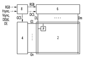
도 1은 본 발명의 실시 예에 따른 표시장치의 구성을 개략적으로 도시한 블록도이다.
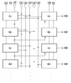
도 2는 실시 예의 게이트 구동회로를 도시한 도면이다.
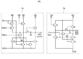
도 3은 실시 예의 게이트 구동회로의 제1 스테이지의 구성을 도시한 도면이다.
도 4는 실시 예의 게이트 구동회로 입력신호 및 출력신호를 도시한 도면이다.1 is a block diagram schematically showing a configuration of a display apparatus according to an embodiment of the present invention.
2 is a diagram showing a gate drive circuit of the embodiment.
3 is a diagram showing the configuration of the first stage of the gate drive circuit of the embodiment.
4 is a diagram showing the gate drive circuit input signal and output signal of the embodiment.
본 발명의 이점 및 특징, 그리고 그것들을 달성하는 방법은 첨부되는 도면과 함께 상세하게 후술되어 있는 실시 예들을 참조하면 명확해질 것이다. 그러나 본 발명은 이하에서 개시되는 실시 예들에 한정되는 것이 아니라 서로 다른 다양한 형태로 구현될 것이며, 단지 본 실시 예들은 본 발명의 개시가 완전하도록 하며, 본 발명이 속하는 기술 분야에서 통상의 지식을 가진 자에게 발명의 범주를 완전하게 알려주기 위해 제공되는 것이며, 본 발명은 청구항의 범주에 의해 정의될 뿐이다.BRIEF DESCRIPTION OF THE DRAWINGS The advantages and features of the present invention and the manner of achieving them will become apparent with reference to the embodiments described in detail below with reference to the accompanying drawings. The present invention may, however, be embodied in many different forms and should not be construed as being limited to the embodiments set forth herein. Rather, these embodiments are provided so that this disclosure will be thorough and complete, and will fully convey the concept of the invention to those skilled in the art. To fully disclose the scope of the invention to a person skilled in the art, and the invention is only defined by the scope of the claims.
본 발명의 실시 예를 설명하기 위한 도면에 개시된 형상, 크기, 비율, 각도, 개수 등은 예시적인 것이므로 본 발명이 도시된 사항에 한정되는 것은 아니다. 명세서 전체에 걸쳐 동일 참조 부호는 동일 구성 요소를 지칭한다. 또한, 본 발명을 설명함에 있어서, 관련된 공지 기술에 대한 구체적인 설명이 본 발명의 요지를 불필요하게 흐릴 수 있다고 판단되는 경우 그 상세한 설명은 생략한다.The shapes, sizes, ratios, angles, numbers, and the like disclosed in the drawings for describing the embodiments of the present invention are illustrative, and thus the present invention is not limited thereto. Like reference numerals refer to like elements throughout the specification. In the following description, well-known functions or constructions are not described in detail since they would obscure the invention in unnecessary detail.
본 명세서 상에서 언급한 '포함한다', '갖는다', '이루어진다' 등이 사용되는 경우 '~만'이 사용되지 않는 이상 다른 부분이 추가될 수 있다. 구성 요소를 단수로 표현한 경우에 특별히 명시적인 기재 사항이 없는 한 복수를 포함하는 경우를 포함한다.In the case where the word 'includes', 'having', 'done', etc. are used in this specification, other parts can be added unless '~ only' is used. Unless the context clearly dictates otherwise, including the plural unless the context clearly dictates otherwise.
구성 요소를 해석함에 있어서, 별도의 명시적 기재가 없더라도 오차 범위를 포함하는 것으로 해석한다.In interpreting the constituent elements, it is construed to include the error range even if there is no separate description.
위치 관계에 대한 설명일 경우, 예를 들어, '~상에', '~상부에', '~하부에', '~옆에' 등으로 두 부분의 위치 관계가 설명되는 경우, '바로' 또는 '직접'이 사용되지 않는 이상 두 부분 사이에 하나 이상의 다른 부분이 위치할 수도 있다.In the case of a description of the positional relationship, for example, if the positional relationship between two parts is described as 'on', 'on top', 'under', and 'next to' Or " direct " is not used, one or more other portions may be located between the two portions.
시간 관계에 대한 설명일 경우, 예를 들어, '~후에', '~에 이어서', '~다음에', '~전에' 등으로 시간 적 선후 관계가 설명되는 경우, '바로' 또는 '직접'이 사용되지 않는 이상 연속적이지 않은 경우도 포함할 수 있다.In the case of a description of a temporal relationship, for example, if a temporal posterior relationship is described by 'after', 'after', 'after', 'before', etc., 'May not be contiguous unless it is used.
제1, 제2 등이 다양한 구성요소들을 서술하기 위해서 사용되나, 이들 구성요소들은 이들 용어에 의해 제한되지 않는다. 이들 용어들은 단지 하나의 구성요소를 다른 구성요소와 구별하기 위하여 사용하는 것이다. 따라서, 이하에서 언급되는 제1 구성요소는 본 발명의 기술적 사상 내에서 제2 구성요소일 수도 있다.The first, second, etc. are used to describe various components, but these components are not limited by these terms. These terms are used only to distinguish one component from another. Therefore, the first component mentioned below may be the second component within the technical spirit of the present invention.
본 발명의 여러 실시 예들의 각각 특징들이 부분적으로 또는 전체적으로 서로 결합 또는 조합 가능하고, 기술적으로 다양한 연동 및 구동이 가능하며, 각 실시 예들이 서로에 대하여 독립적으로 실시 가능할 수도 있고 연관 관계로 함께 실시할 수도 있다.It is to be understood that each of the features of the various embodiments of the present invention may be combined or combined with each other, partially or wholly, technically various interlocking and driving, and that the embodiments may be practiced independently of each other, It is possible.
이하, 본 발명의 실시 예들은 도면을 참고하여 상세하게 설명한다. 그리고 도면들에 있어서, 장치의 크기 및 두께 등은 편의를 위하여 과장되어 표현될 수도 있다. 명세서 전체에 걸쳐서 동일한 참조번호들은 동일한 구성요소들을 나타낸다.Hereinafter, embodiments of the present invention will be described in detail with reference to the drawings. In the drawings, the size and thickness of the device may be exaggerated for convenience. Like reference numerals designate like elements throughout the specification.
도 1은 본 발명의 실시 예에 따른 표시장치의 구성을 개략적으로 도시한 블록도이고, 도 2는 실시 예의 게이트 구동회로를 도시한 도면이고, 도 3은 실시 예의 게이트 구동회로의 제1 스테이지의 구성을 도시한 도면이다.FIG. 1 is a block diagram schematically showing a configuration of a display device according to an embodiment of the present invention, FIG. 2 is a view showing a gate drive circuit of the embodiment, and FIG. 3 is a cross- Fig.
도 1 내지 도 3에 도시된 바와 같이, 실시 예의 표시장치는 유기 발광 표시장치(OLED)일 수 있으나, 이에 한정되는 것은 아니다. 예컨대 상기 표시장치는 액정표시장치(LCD, 전계방출 표시장치(FED), 플라즈마 디스플레이 패널(PDP), 전기영동 표시장치(EPD)일 수 있다.As shown in FIGS. 1 to 3, the display device of the embodiment may be an organic light emitting diode (OLED), but is not limited thereto. For example, the display device may be a liquid crystal display (LCD), a field emission display (FED), a plasma display panel (PDP), or an electrophoretic display (EPD).
상기 표시장치는 표시패널(2), 타이밍 컨트롤러(8), 게이트 구동회로(4) 및 데이터 구동회로(6)를 포함할 수 있다.The display device may include a
상기 표시패널(2)은 표시영역과 비표시영역으로 구분될 수 있다. 상기 표시패널(2)은 복수의 게이트 라인(G1 내지 Gn) 및 복수의 데이터 라인(D1 내지 Dm)과 상기 복수의 게이트 라인(G1 내지 Gn) 및 복수의 데이터 라인(D1 내지 Dm)의 교차영역 마다 배치된 픽셀(P)을 포함할 수 있다. 여기서, 상기 픽셀(P)은 광을 발광하는 유기발광소자 및 상기 유기발광소자를 구동하는 구동소자들을 포함할 수 있다.The
상기 표시패널(2)이 액정층을 포함하는 액정표시패널일 경우, 상기 액정표시패널은 서로 대면되는 제1 및 제2 투명기판과 상기 제1 및 제2 투명기판 사이의 액정층을 포함할 수 있다. 상기 액정표시패널은 복수의 게이트 라인(G1 내지 Gn) 및 복수의 데이터 라인(D1 내지 Dm)을 포함할 수 있고, 상기 복수의 게이트 라인(G1 내지 Gn)과 복수의 데이터 라인(D1 내지 Dm)의 교차영역에 위치한 트랜지스터를 포함하고, 상기 트랜지스터들에 각각 접속된 액정셀, 화소전극, 및 스토리지 캐패시터 등을 포함할 수 있다.When the
상기 타이밍 컨트롤러(8)는 외부로부터 입력되는 RGB 데이터(RGB)를 표시패널(2)의 크기 및 해상도 등에 알맞게 정렬하고 정렬된 디지털 영상 데이터를 데이터 구동회로(6)에 공급한다. 상기 타이밍 컨트롤러(8)는 외부로부터 입력되는 동기신호들 예를 들어, 도트클럭(DCLK), 데이터 인에이블 신호(DE), 수평 동기신호(Hsync), 수직 동기 신호(Vsync) 등을 이용하여 게이트 제어신호(GCS) 및 데이터 제어신호(DCS)를 생성하고 이를 게이트 구동회로(4)와 데이터 구동회로(6)에 각각 공급한다.The
상기 데이터 구동회로(6)는 COG(Chip on Glass)방식으로 표시패널(2) 내에 실장될 수 있다. 상기 데이터 구동회로(6)는 상기 데이터 제어신호 중 소스 스타트 펄스(SSP; Source Start Pulse)와 소스 쉬프트 클럭(SSC; Source Shift Clock) 등을 이용하여 타이밍 컨트롤러(8)로부터 입력되는 디지털 영상 데이터를 아날로그의 데이터 전압으로 변환한다. 그리고, 소스 출력 인에이블(SOE; Source Output Enable) 신호에 응답하여 데이터 전압을 각 데이터 라인(D1 내지 Dm)에 공급한다.The
상기 게이트 구동회로(4)는 상기 게이트 제어신호(GCS)를 이용하여 상기 게이트 라인(G1 내지 Gn)에 스캔신호 및 에미션 신호를 공급할 수 있다. 상기 게이트 제어신호는 한 화면이 표시되는 1 수직기간 중에서 스캔이 시작되는 시작 게이트 라인을 지시하는 게이트 스타트 펄스(GSP; Gate Start Pulse)와 쉬프트레지스터(41a, 41b, 41c, 41d)에 입력되어 게이트 스타트 펄스(GSP)를 순차적으로 쉬프트시키기 위한 타이밍 제어신호로써 화소(P) 내 트랜지스터의 온(ON) 기간에 대응하는 펄스폭으로 발생되는 게이트 쉬프트 클럭(GSC; Gate Shift Clock), 게이트 구동회로(4)의 출력을 지시하는 게이트 출력 인에이블(GOE; Gate Output Enable) 신호를 포함할 수 있다.The
실시 예의 게이트 구동회로(4)는 GIP(Gate In Panel) 방식으로 표시패널(2)의 비표시영역 내에 실장될 수 있다. The
실시 예의 게이트 구동회로(4)는 복수의 쉬프트레지스터(41a, 41b, 41c, 41d) 및 복수의 인버터(43a, 43b, 43c, 43d)를 포함할 수 있다. 상기 복수의 쉬프트레지스터(41a, 41b, 41c, 41d)는 상기 게이트 제어신호를 이용하여 스캔신호(SCAN1)를 생성하고, 상기 복수의 인버터(43a, 43b, 43c, 43d)는 상기 게이트 제어신호 및 상기 스캔신호를 에미션 신호(EM1)를 생성할 수 있다. 여기서, 상기 복수의 쉬프트레지스터(41a, 41b, 41c, 41d) 및 복수의 인버터(43a, 43b, 43c, 43d)는 제1 내지 제5 클럭신호(CLK1 내지 CLK5)를 공유할 수 있다. 실시 예는 상기 복수의 쉬프트레지스터(41a, 41b, 41c, 41d) 및 복수의 인버터(43a, 43b, 43c, 43d)는 제1 내지 제5 클럭신호(CLK1 내지 CLK5)를 공유함으로써, 클럭신호 배선을 5개까지 줄일 수 있다. 상기 제1 내지 제5 클럭신호(CLK1 내지 CLK5)는 5가지 위상을 가질 수 있다. 실시 예의 복수의 쉬프트레지스터(41a, 41b, 41c, 41d) 및 복수의 인버터(43a, 43b, 43c, 43d)는 5가지 위상의 제1 내지 제5 클럭신호(CLK1 내지 CLK5)을 공유할 수 있다. 상기 게이트 구동회로(4)는 제1 쉬프트레지스터(41a)에 제공되는 게이트 스타트 펄스(GSP)가 입력되는 게이트 스타트 펄스 입력단자(VST) 및 게이트 스타트 펄스 입력배선을 더 포함할 수 있다.The
실시 예는 게이트 스타트 펄스(GSP)를 제외한 클럭신호들을 공유하는 복수의 쉬프트레지스터(41a, 41b, 41c, 41d) 및 복수의 인버터(43a, 43b, 43c, 43d)를 포함하는 게이트 구동회로(4) 구조에 의해 일반적인 게이트 구동회로보다 클럭배선을 8개에서 5개로 줄여 게이트 구동회로(4)의 배선구조를 간소화할 수 있다.The embodiment includes a plurality of
실시 예는 게이트 구동회로(4)의 배선구조를 간소화하여 네로우 베젤(narrow bezel)을 구현할 수 있는 효과가 있다.The embodiment has the effect of simplifying the wiring structure of the
예컨대, 제1 스테이지(STG1)을 일예로 설명하면, 제1 쉬프트레지스트(41a)는 클럭단자에 제1 클럭신호(CLK1), 제3 클럭신호(CLK3) 및 제5 클럭신호(CLK5)가 제공되고, 제1 인버터(43a)는 클럭단자에 제2 클럭신호(CLK2)가 제공될 수 있다.For example, the
상기 제1 쉬프트 레지스트(41a)는 제1 내지 제9 트랜지스터(T1 내지 T9) 및 제1 구동 캐패시터(CB1)를 포함할 수 있다. The first shift resists 41a may include first to ninth transistors T1 to T9 and a first driving capacitor CB1.
상기 제1 트랜지스터(T1)는 게이트 스타트 펄스(VST)와 게이트 전극이 접속되고, 고전위전압(VDD)과 드레인 전극이 접속되고, 제2 트랜지스터(T2)의 드레인전극에 소스전극이 접속된다.The first transistor T1 has a gate start pulse VST and a gate electrode connected to each other, a high potential voltage VDD and a drain electrode connected to each other, and a source electrode connected to a drain electrode of the second transistor T2.
상기 제2 트랜지스터(T2)는 제5 클럭신호(CLK5)가 입력되는 클럭단자에 게이트전극이 접속되고, 상기 제1 트랜지스터(T1)의 소스전극에 드레이전극이 접속되고, Q1노드(Q1)에 소스전극이 접속된다.A gate electrode of the second transistor T2 is connected to a clock terminal to which a fifth clock signal CLK5 is input. A drain electrode of the second transistor T2 is connected to a source electrode of the first transistor T1. And the source electrode is connected.
상기 제3 트랜지스터(T3)는 QB1노드(QB1)에 게이트전극이 접속되고, 제4 트랜지스터(T4)의 소스전극에 드레인 전극이 접속되고, 저전위전압(VSS)에 소스전극이 접속된다.The third transistor T3 has a gate electrode connected to the QB1 node QB1, a drain electrode connected to the source electrode of the fourth transistor T4, and a source electrode connected to the low potential voltage VSS.
상기 제4 트랜지스터(T4)는 고전위전압(VDD)에 게이트전극이 접속되고, 제3 트랜지스터(T3)의 드레인전극에 소스전극이 접속되고, 상기 제2 트랜지스터(T2)의 소스전극에 드레인전극이 접속된다.The fourth transistor T4 has a gate electrode connected to the high-potential voltage VDD, a source electrode connected to the drain electrode of the third transistor T3, a source electrode connected to the drain electrode of the second transistor T2, .
상기 제5 트랜지스터(T5)는 제3 클럭신호(CLK3)가 공급되는 단지에 게이트전극이 접속되고, 고전위전압(VDD)에 드레인전극이 접속되고, QB1노드(QB1)에 소스전극이 접속된다.The fifth transistor T5 is connected to the gate electrode of the fifth transistor T5 through which the third clock signal CLK3 is supplied, the drain electrode of the fifth transistor T5 is connected to the high potential voltage VDD, and the source electrode of the fifth transistor T5 is connected to the QB1 node QB1 .
상기 제6 트랜지스터(T6)는 게이트 스타트 펄스(VST)에 게이트전극이 접속되고, 제5 트랜지스터(T5)의 소스전극에 드레인전극이 접속되고, 저전위전압(VSS)에 소스전극이 접속된다.The sixth transistor T6 has a gate electrode connected to the gate start pulse VST, a drain electrode connected to the source electrode of the fifth transistor T5, and a source electrode connected to the low-potential voltage VSS.
상기 제7 트랜지스터(T7)는 상기 제4 트랜지스터(T4)의 소스전극에 게이트전극이 접속되고, QB1노드(QB1)에 드레인전극이 접속되고, 저전위전압(VSS)에 소스전극이 접속된다.The seventh transistor T7 has a gate electrode connected to the source electrode of the fourth transistor T4, a drain electrode connected to the QB1 node QB1, and a source electrode connected to the low potential VSS.
상기 제8 트랜지스터(T8)는 Q1노드(Q1)에 게이트전극이 접속되고, 제1 클럭신호(CLK1)가 공급되는 단자에 드레인전극이 접속되고, 게이트 라인에 제공되는 스캔신호(SCAN1)가 출력되는 출력노드(Vout1)와 소스전극이 접속된다. 여기서 게이트 전극과 소스전극 사이에는 제1 구동 캐패시터(CB1)가 위치한다.A gate electrode of the eighth transistor T8 is connected to the Q1 node Q1. A drain electrode of the eighth transistor T8 is connected to a terminal to which the first clock signal CLK1 is supplied. A scan signal SCAN1, And the output node Vout1 is connected to the source electrode. A first driving capacitor CB1 is disposed between the gate electrode and the source electrode.
상기 제9 트랜지스터(T9)는 QB1노드(QB1)에 게이트전극이 접속되고, 제8 트랜지스터(T8)의 소스전극에 드레인 전극이 접속되고, 저전위 전압(VSS)에 소스전극이 접속된다.In the ninth transistor T9, a gate electrode is connected to the QB1 node QB1, a drain electrode is connected to the source electrode of the eighth transistor T8, and a source electrode is connected to the low potential voltage VSS.
상기 제1 인버터(43a)는 제10 내지 제15 트랜지스터(T10 내지 T15) 및 제2 구동 캐패시터(CB2)를 포함할 수 있다. The
상기 제10 트랜지스터(T10)는 제2 클럭신호(CLK2)가 공급되는 단자에 게이트전극이 접속되고, 고전위전압(VDD)에 드레인전극이 접속되고, Q2노드(Q2)에 소스전극이 접속된다.In the tenth transistor T10, a gate electrode is connected to a terminal to which the second clock signal CLK2 is supplied, a drain electrode is connected to the high-potential voltage VDD, and a source electrode is connected to the Q2 node Q2 .
상기 제11 트랜지스터(T11)는 QB2노드(QB2)에 게이트전극이 접속되고, Q2노드(Q2)에 드레인전극이 접속되고, 저전위전압(VSS)에 소스전극이 접속된다.In the eleventh transistor T11, a gate electrode is connected to the QB2 node QB2, a drain electrode is connected to the Q2 node Q2, and a source electrode is connected to the low potential voltage VSS.
상기 제12 트랜지스터(T12)는 에미션 신호(EM1) 출력라인에 게이트전극이 접속되고, 고전위전압(VDD)에 드레인전극이 접속되고, 제14 트랜지스터(T14)의 소스전극 및 제15 트랜지스터(T15)의 드레인전극에 소스전극이 접속된다.The twelfth transistor T12 has a gate electrode connected to the emission signal EM1 output line, a drain electrode connected to the high potential voltage VDD, a source electrode of the fourteenth transistor T14, T15) is connected to the drain electrode of the transistor T15.
상기 제13 트랜지스터(T13)는 Q2노드(Q2)에 게이트전극이 접속되고, 고전위전압(VDD)에 드레인전극이 접속되고, 에미션 신호(EM1) 출력라인(Vout2)에 소스전극이 접속된다. 여기서, 상기 제13 트랜지스터(T13)의 게이트전극과 소스전극 사이에는 제2 구동 캐패시터(CB2)가 배치된다.In the thirteenth transistor T13, a gate electrode is connected to the Q2 node Q2, a drain electrode is connected to the high potential voltage VDD, and a source electrode is connected to the emission signal EM1 output line Vout2 . A second driving capacitor CB2 is disposed between the gate electrode and the source electrode of the thirteenth transistor T13.
상기 제14 트랜지스터(T14)는 QB2노드(QB2)에 게이트전극이 접속되고, 에미션 신호(EM1) 출력라인에 드레인전극이 접속되고, 제12 트랜지스터(T12)의 소스전극에 소스전극이 접속된다.The 14th transistor T14 has a gate electrode connected to the QB2 node QB2, a drain electrode connected to the emission signal EM1 output line, and a source electrode connected to the source electrode of the 12th transistor T12 .
상기 제15 트랜지스터(T15)는 QB2노드(QB2)에 게이트전극이 접속되고, 상기 제14 트랜지스터(T14)의 소스전극에 드레인전극이 접속되고, 저전위전압(VSS)에 소스전극이 접속된다.In the fifteenth transistor T15, a gate electrode is connected to the QB2 node QB2, a drain electrode is connected to the source electrode of the fourteenth transistor T14, and a source electrode is connected to the low potential voltage VSS.
도 4는 실시 예의 게이트 구동회로 입력신호 및 출력신호를 도시한 도면이다.4 is a diagram showing the gate drive circuit input signal and output signal of the embodiment.
도 2 내지 도 4에 도시된 바와 같이, 실시 예의 게이트 구동회로는 제1 스테이지(STG1)에서 제1 쉬프트레지스터(41a)에 게이트 스타트 펄스(VST) 및 제5 클럭신호(CLK5)가 동기되어 입력되면, 제1 및 제2 트랜지스터(T1,T2)가 턴-온되어 Q1노드(Q1)에 하이(High) 상태가 된다. 또한, 상기 QB1노드(QB1)는 로우(Low)상태가 된다.2 to 4, in the gate driving circuit of the embodiment, the gate start pulse VST and the fifth clock signal CLK5 are synchronized with the
다음 제2 구간(a2)은 제1 클럭신호(CLK1)이 입력되면, 출력노드(Vout)로 하이(High)가 출력되고, Q1노드(Q1)는 제1 구동 캐패시터(CB1)에 의해 부트스트래핑(Bootstrapping)될 수 있다. 제1 인버터(43a)는 출력노드(Vout)로 하이(High)에 의해 제14 트랜지스터(T14)가 턴-온되어 에미션 신호(EM1)는 로우(Low) 상태가 된다. 이때, 제11 트랜지스터(T11)가 턴-온되어 제13 트랜지스터(T13)이 턴-오프된다.In the next second period a2, when the first clock signal CLK1 is inputted, a high level is outputted to the output node Vout, and the Q1 node Q1 is bootstrapped by the first driving capacitor CB1. (Bootstrapping). The
다음 제3 구간(a3)은 제2 클럭신호(CLK2)이 입력되면, 제13 트랜지스터(T13)가 턴-온되고, 에미션 신호(EM1)는 하이(High) 상태가 된다. 이후, 제1 클럭신호(CLK1)이 입력되어 에미션 신호(EM1)는 로우(Low) 상태가 된다.In the next third period a3, when the second clock signal CLK2 is input, the thirteenth transistor T13 is turned on and the emission signal EM1 becomes high. Thereafter, the first clock signal CLK1 is input and the emission signal EM1 becomes low.
다음 제4 구간(a4)은 제1 쉬프트레지스터(41a)에 제3 클럭신호(CLK3)가 입력되면, 제3 트랜지스터(T3) 및 제5 트랜지스터(T5)가 턴-온되어 QB1노드(QB1)는 하이(High)가 되고, Q1노드(Q1)는 로우(Low) 상태가 된다. 이후, 제2 클럭신호(CLK2)가 입력되어 에미션 신호(EM1)는 하이(High) 상태가 된다.In the next fourth period a4, when the third clock signal CLK3 is input to the
다음 제5 구간(a5)은 제3 클럭신호(CLK3)가 입력되고, QB1노드(QB1)는 하이(High) 상태이므로 에미션 신호(EM1)는 하이(High) 상태는 유지된다. Since the third clock signal CLK3 is input in the fifth period a5 and the QB1 node QB1 is in the high state, the emission signal EM1 is maintained in the high state.
실시 예는 상기 복수의 쉬프트레지스터(41a, 41b, 41c, 41d) 및 복수의 인버터(43a, 43b, 43c, 43d)는 제1 내지 제5 클럭신호(CLK1 내지 CLK5)를 공유함으로써, 클럭신호 배선을 5개까지 줄일 수 있다. 실시 예는 게이트 스타트 펄스를 제외한 클럭신호들을 공유하는 복수의 쉬프트레지스터(41a, 41b, 41c, 41d) 및 복수의 인버터(43a, 43b, 43c, 43d)를 포함하는 게이트 구동회로 구조에 의해 일반적인 게이트 구동회로보다 클럭배선을 8개에서 5개로 줄여 게이트 구동회로(4)의 배선구조를 간소화할 수 있다.In the embodiment, the plurality of
실시 예는 게이트 구동회로(4)의 배선구조를 간소화하여 네로우 베젤(narrow bezel)을 구현할 수 있는 효과가 있다.The embodiment has the effect of simplifying the wiring structure of the
이상에서 실시 예들에 설명된 특징, 구조, 효과 등은 적어도 하나의 실시 예에 포함되며, 반드시 하나의 실시 예에만 한정되는 것은 아니다. 나아가, 각 실시 예에서 예시된 특징, 구조, 효과 등은 실시 예들이 속하는 분야의 통상의 지식을 가지는 자에 의해 다른 실시 예들에 대해서도 조합 또는 변형되어 실시 가능하다. 따라서 이러한 조합과 변형에 관계된 내용들은 실시 예의 범위에 포함되는 것으로 해석되어야 할 것이다.The features, structures, effects and the like described in the embodiments are included in at least one embodiment and are not necessarily limited to one embodiment. Further, the features, structures, effects, and the like illustrated in the embodiments can be combined and modified by other persons having ordinary skill in the art to which the embodiments belong. Accordingly, the contents of such combinations and modifications should be construed as being included in the scope of the embodiments.
이상에서 실시 예를 중심으로 설명하였으나 이는 단지 예시일 뿐 실시 예를 한정하는 것이 아니며, 실시 예가 속하는 분야의 통상의 지식을 가진 자라면 본 실시 예의 본질적인 특성을 벗어나지 않는 범위에서 이상에 예시되지 않은 여러 가지의 변형과 응용이 가능함을 알 수 있을 것이다. 예를 들어, 실시 예에 구체적으로 나타난 각 구성 요소는 변형하여 실시할 수 있는 것이다. 그리고 이러한 변형과 응용에 관계된 차이점들은 첨부된 청구 범위에서 설정하는 실시 예의 범위에 포함되는 것으로 해석되어야 할 것이다.While the present invention has been particularly shown and described with reference to exemplary embodiments thereof, it will be understood by those skilled in the art that various changes in form and details may be made therein without departing from the spirit and scope of the invention. It can be seen that the modification and application of branches are possible. For example, each component specifically shown in the embodiments can be modified and implemented. It is to be understood that the present invention may be embodied in many other specific forms without departing from the spirit or essential characteristics thereof.
4: 게이트 구동회로
41a, 41b, 41c, 41d: 복수의 쉬프트레지스터
43a, 43b, 43c, 43d: 복수의 인버터4: Gate drive circuit
41a, 41b, 41c and 41d: a plurality of shift registers
43a, 43b, 43c, 43d:
Claims (6)
상기 복수의 클럭신호라인으로부터 복수의 클럭신호를 입력받고 스캔신호를 생성하는 쉬프트레지스터; 및
상기 복수의 클럭신호를 입력받고 에미션 신호를 생성하는 인버터를 포함하고,
상기 쉬프트레지스터 및 인버터는 복수의 클럭신호를 공유하는 게이트 구동회로.
A plurality of clock signal lines;
A shift register for receiving a plurality of clock signals from the plurality of clock signal lines and generating a scan signal; And
And an inverter for receiving the plurality of clock signals and generating an emission signal,
Wherein the shift register and the inverter share a plurality of clock signals.
상기 쉬프트레지스터의 스타트 타이밍 신호를 제공하는 게이트 스타트 펄스 입력단자 및 입력배선을 더 포함하는 게이트 구동회로.
The method according to claim 1,
Further comprising a gate start pulse input terminal for providing a start timing signal of said shift register and an input wiring.
상기 복수의 클럭신호는 5가지 위상을 갖는 게이트 구동회로.
The method according to claim 1,
Wherein the plurality of clock signals have five phases.
복수의 화소를 갖는 표시패널; 및
상기 표시패널의 가장자리에 복수의 클럭신호라인 및 상기 복수의 클럭신호라인으로부터 복수의 클럭신호를 입력받고 스캔신호를 생성하는 쉬프트레지스터 및 상기 복수의 클럭신호를 입력받고 에미션신호를 생성하는 인버터를 포함하는 게이트 구동회로;
상기 게이트 구동회로는 상기 쉬프트레지스터 및 인버터는 복수의 클럭신호를 공유하는 표시장치.
A timing controller for generating a plurality of clock signals and a gate control signal;
A display panel having a plurality of pixels; And
A shift register for receiving a plurality of clock signal lines at an edge of the display panel and a plurality of clock signals from the plurality of clock signal lines and generating a scan signal, and an inverter for receiving the plurality of clock signals and generating an emission signal, A gate driving circuit including the gate driving circuit;
And the gate driver circuit shares the plurality of clock signals with the shift register and the inverter.
상기 쉬프트레지스터의 스타트 타이밍 신호를 제공하는 게이트 스타트 펄스 입력단자 및 입력배선을 더 포함하는 표시장치.
5. The method of claim 4,
And a gate start pulse input terminal for providing a start timing signal of the shift register and an input wiring.
상기 복수의 클럭신호는 5가지 위상을 갖는 표시장치.
5. The method of claim 4,
Wherein the plurality of clock signals have five phases.
Priority Applications (1)
| Application Number | Priority Date | Filing Date | Title |
|---|---|---|---|
| KR1020150189784A KR102478374B1 (en) | 2015-12-30 | 2015-12-30 | Gate draiver and display device having the same |
Applications Claiming Priority (1)
| Application Number | Priority Date | Filing Date | Title |
|---|---|---|---|
| KR1020150189784A KR102478374B1 (en) | 2015-12-30 | 2015-12-30 | Gate draiver and display device having the same |
Publications (2)
| Publication Number | Publication Date |
|---|---|
| KR20170079338A true KR20170079338A (en) | 2017-07-10 |
| KR102478374B1 KR102478374B1 (en) | 2022-12-15 |
Family
ID=59355272
Family Applications (1)
| Application Number | Title | Priority Date | Filing Date |
|---|---|---|---|
| KR1020150189784A KR102478374B1 (en) | 2015-12-30 | 2015-12-30 | Gate draiver and display device having the same |
Country Status (1)
| Country | Link |
|---|---|
| KR (1) | KR102478374B1 (en) |
Cited By (2)
| Publication number | Priority date | Publication date | Assignee | Title |
|---|---|---|---|---|
| KR20190057641A (en) * | 2017-11-20 | 2019-05-29 | 엘지디스플레이 주식회사 | Clock signals and Gate drive circuit using the same |
| CN110085172A (en) * | 2018-06-14 | 2019-08-02 | 友达光电股份有限公司 | Gate drive apparatus |
Citations (3)
| Publication number | Priority date | Publication date | Assignee | Title |
|---|---|---|---|---|
| KR100748321B1 (en) * | 2006-04-06 | 2007-08-09 | 삼성에스디아이 주식회사 | Scan driving circuit and organic light emitting display using the same |
| KR20120040811A (en) * | 2010-10-20 | 2012-04-30 | 엘지디스플레이 주식회사 | Gate driver and organic light emitting diode display including the same |
| KR20130051340A (en) * | 2011-11-09 | 2013-05-20 | 엘지디스플레이 주식회사 | Organic light emitting display having shift resigter sharing cluck lines |
-
2015
- 2015-12-30 KR KR1020150189784A patent/KR102478374B1/en active IP Right Grant
Patent Citations (3)
| Publication number | Priority date | Publication date | Assignee | Title |
|---|---|---|---|---|
| KR100748321B1 (en) * | 2006-04-06 | 2007-08-09 | 삼성에스디아이 주식회사 | Scan driving circuit and organic light emitting display using the same |
| KR20120040811A (en) * | 2010-10-20 | 2012-04-30 | 엘지디스플레이 주식회사 | Gate driver and organic light emitting diode display including the same |
| KR20130051340A (en) * | 2011-11-09 | 2013-05-20 | 엘지디스플레이 주식회사 | Organic light emitting display having shift resigter sharing cluck lines |
Cited By (3)
| Publication number | Priority date | Publication date | Assignee | Title |
|---|---|---|---|---|
| KR20190057641A (en) * | 2017-11-20 | 2019-05-29 | 엘지디스플레이 주식회사 | Clock signals and Gate drive circuit using the same |
| CN110085172A (en) * | 2018-06-14 | 2019-08-02 | 友达光电股份有限公司 | Gate drive apparatus |
| CN110085172B (en) * | 2018-06-14 | 2020-10-09 | 友达光电股份有限公司 | Gate driving device |
Also Published As
| Publication number | Publication date |
|---|---|
| KR102478374B1 (en) | 2022-12-15 |
Similar Documents
| Publication | Publication Date | Title |
|---|---|---|
| US10276121B2 (en) | Gate driver with reduced number of thin film transistors and display device including the same | |
| KR102505897B1 (en) | OLED Display Panel | |
| US10319283B2 (en) | Gate driving circuit and display device including the same | |
| KR102156769B1 (en) | Display device and gate shift resgister initialting method of the same | |
| US9430981B2 (en) | Display panel | |
| US8982032B2 (en) | Display device with integrated touch screen including pull-up and pull-down transistors and method of driving the same | |
| KR101857808B1 (en) | Scan Driver and Organic Light Emitting Display Device using thereof | |
| KR20190037860A (en) | Gate driver and Flat Panel Display Device including the same | |
| KR101924427B1 (en) | Organic Light Emitting Display having shift resigter sharing cluck lines | |
| TWI584248B (en) | Gate driving circuit and display device using the same | |
| US9941018B2 (en) | Gate driving circuit and display device using the same | |
| US10198987B2 (en) | Gate driving circuit | |
| JP2019504335A (en) | GIP circuit, driving method thereof, and flat panel display device | |
| KR20230110687A (en) | Gate driving circuit and display device using the same | |
| KR20120117120A (en) | Pulse output circuit and organic light emitting diode display device using the same | |
| KR102478374B1 (en) | Gate draiver and display device having the same | |
| KR20170034204A (en) | Display device | |
| KR20160081649A (en) | Gata driver and touch screen integrated display device including thereof | |
| KR20150066981A (en) | Display device | |
| KR20180067948A (en) | Shift register and gate driving circuit including the same | |
| KR102436560B1 (en) | Gate driving circuit and organic light emitting display using the same | |
| KR101918151B1 (en) | Shift register and display device including the same | |
| KR20190036447A (en) | Display panel and Organic Light Emitting Diode display device using the same | |
| KR102283377B1 (en) | Display device and gate driving circuit thereof | |
| KR102534740B1 (en) | Gate driver and display device including thereof |
Legal Events
| Date | Code | Title | Description |
|---|---|---|---|
| A201 | Request for examination | ||
| E902 | Notification of reason for refusal | ||
| E601 | Decision to refuse application | ||
| GRNT | Written decision to grant |