KR20170047953A - Semiconductor device and method of fabricating the same - Google Patents
Semiconductor device and method of fabricating the same Download PDFInfo
- Publication number
- KR20170047953A KR20170047953A KR1020150148710A KR20150148710A KR20170047953A KR 20170047953 A KR20170047953 A KR 20170047953A KR 1020150148710 A KR1020150148710 A KR 1020150148710A KR 20150148710 A KR20150148710 A KR 20150148710A KR 20170047953 A KR20170047953 A KR 20170047953A
- Authority
- KR
- South Korea
- Prior art keywords
- gate electrode
- spacers
- gate
- spacer
- stress
- Prior art date
Links
- 239000004065 semiconductor Substances 0.000 title abstract description 54
- 238000004519 manufacturing process Methods 0.000 title abstract description 17
- 125000006850 spacer group Chemical group 0.000 claims abstract description 234
- 239000000758 substrate Substances 0.000 claims abstract description 41
- 239000011229 interlayer Substances 0.000 claims abstract description 36
- 230000003647 oxidation Effects 0.000 claims description 32
- 238000007254 oxidation reaction Methods 0.000 claims description 32
- 229910052751 metal Inorganic materials 0.000 claims description 31
- 239000002184 metal Substances 0.000 claims description 31
- 238000000034 method Methods 0.000 claims description 17
- 239000010410 layer Substances 0.000 description 51
- XUIMIQQOPSSXEZ-UHFFFAOYSA-N Silicon Chemical compound [Si] XUIMIQQOPSSXEZ-UHFFFAOYSA-N 0.000 description 14
- 229910052710 silicon Inorganic materials 0.000 description 14
- 239000010703 silicon Substances 0.000 description 14
- 230000006870 function Effects 0.000 description 12
- 150000001875 compounds Chemical class 0.000 description 11
- VYPSYNLAJGMNEJ-UHFFFAOYSA-N Silicium dioxide Chemical compound O=[Si]=O VYPSYNLAJGMNEJ-UHFFFAOYSA-N 0.000 description 10
- 238000010586 diagram Methods 0.000 description 9
- 229910052814 silicon oxide Inorganic materials 0.000 description 9
- 239000000463 material Substances 0.000 description 8
- 238000010438 heat treatment Methods 0.000 description 7
- 229910052581 Si3N4 Inorganic materials 0.000 description 6
- 230000001154 acute effect Effects 0.000 description 6
- HQVNEWCFYHHQES-UHFFFAOYSA-N silicon nitride Chemical compound N12[Si]34N5[Si]62N3[Si]51N64 HQVNEWCFYHHQES-UHFFFAOYSA-N 0.000 description 6
- ATJFFYVFTNAWJD-UHFFFAOYSA-N Tin Chemical compound [Sn] ATJFFYVFTNAWJD-UHFFFAOYSA-N 0.000 description 4
- 230000006835 compression Effects 0.000 description 4
- 238000007906 compression Methods 0.000 description 4
- 230000002093 peripheral effect Effects 0.000 description 4
- 230000000903 blocking effect Effects 0.000 description 3
- 230000007423 decrease Effects 0.000 description 3
- OKTJSMMVPCPJKN-UHFFFAOYSA-N Carbon Chemical compound [C] OKTJSMMVPCPJKN-UHFFFAOYSA-N 0.000 description 2
- 229910000577 Silicon-germanium Inorganic materials 0.000 description 2
- 229910004491 TaAlN Inorganic materials 0.000 description 2
- 229910010038 TiAl Inorganic materials 0.000 description 2
- 229910010037 TiAlN Inorganic materials 0.000 description 2
- 229910034327 TiC Inorganic materials 0.000 description 2
- 229910052782 aluminium Inorganic materials 0.000 description 2
- 239000005380 borophosphosilicate glass Substances 0.000 description 2
- 229910052799 carbon Inorganic materials 0.000 description 2
- 238000005530 etching Methods 0.000 description 2
- 229910052732 germanium Inorganic materials 0.000 description 2
- GNPVGFCGXDBREM-UHFFFAOYSA-N germanium atom Chemical compound [Ge] GNPVGFCGXDBREM-UHFFFAOYSA-N 0.000 description 2
- MRELNEQAGSRDBK-UHFFFAOYSA-N lanthanum(3+);oxygen(2-) Chemical compound [O-2].[O-2].[O-2].[La+3].[La+3] MRELNEQAGSRDBK-UHFFFAOYSA-N 0.000 description 2
- 150000004767 nitrides Chemical class 0.000 description 2
- RVTZCBVAJQQJTK-UHFFFAOYSA-N oxygen(2-);zirconium(4+) Chemical compound [O-2].[O-2].[Zr+4] RVTZCBVAJQQJTK-UHFFFAOYSA-N 0.000 description 2
- 229910003468 tantalcarbide Inorganic materials 0.000 description 2
- 229910001928 zirconium oxide Inorganic materials 0.000 description 2
- JBRZTFJDHDCESZ-UHFFFAOYSA-N AsGa Chemical compound [As]#[Ga] JBRZTFJDHDCESZ-UHFFFAOYSA-N 0.000 description 1
- KRHYYFGTRYWZRS-UHFFFAOYSA-M Fluoride anion Chemical compound [F-] KRHYYFGTRYWZRS-UHFFFAOYSA-M 0.000 description 1
- GYHNNYVSQQEPJS-UHFFFAOYSA-N Gallium Chemical compound [Ga] GYHNNYVSQQEPJS-UHFFFAOYSA-N 0.000 description 1
- 229910001218 Gallium arsenide Inorganic materials 0.000 description 1
- 229910000673 Indium arsenide Inorganic materials 0.000 description 1
- GPXJNWSHGFTCBW-UHFFFAOYSA-N Indium phosphide Chemical compound [In]#P GPXJNWSHGFTCBW-UHFFFAOYSA-N 0.000 description 1
- 239000004642 Polyimide Substances 0.000 description 1
- 229910004298 SiO 2 Inorganic materials 0.000 description 1
- BOTDANWDWHJENH-UHFFFAOYSA-N Tetraethyl orthosilicate Chemical compound CCO[Si](OCC)(OCC)OCC BOTDANWDWHJENH-UHFFFAOYSA-N 0.000 description 1
- GWEVSGVZZGPLCZ-UHFFFAOYSA-N Titan oxide Chemical compound O=[Ti]=O GWEVSGVZZGPLCZ-UHFFFAOYSA-N 0.000 description 1
- XWCMFHPRATWWFO-UHFFFAOYSA-N [O-2].[Ta+5].[Sc+3].[O-2].[O-2].[O-2] Chemical compound [O-2].[Ta+5].[Sc+3].[O-2].[O-2].[O-2] XWCMFHPRATWWFO-UHFFFAOYSA-N 0.000 description 1
- LEVVHYCKPQWKOP-UHFFFAOYSA-N [Si].[Ge] Chemical compound [Si].[Ge] LEVVHYCKPQWKOP-UHFFFAOYSA-N 0.000 description 1
- ILCYGSITMBHYNK-UHFFFAOYSA-N [Si]=O.[Hf] Chemical compound [Si]=O.[Hf] ILCYGSITMBHYNK-UHFFFAOYSA-N 0.000 description 1
- 238000007792 addition Methods 0.000 description 1
- 239000004964 aerogel Substances 0.000 description 1
- XAGFODPZIPBFFR-UHFFFAOYSA-N aluminium Chemical compound [Al] XAGFODPZIPBFFR-UHFFFAOYSA-N 0.000 description 1
- 229910052787 antimony Inorganic materials 0.000 description 1
- WATWJIUSRGPENY-UHFFFAOYSA-N antimony atom Chemical compound [Sb] WATWJIUSRGPENY-UHFFFAOYSA-N 0.000 description 1
- QVQLCTNNEUAWMS-UHFFFAOYSA-N barium oxide Chemical class [Ba]=O QVQLCTNNEUAWMS-UHFFFAOYSA-N 0.000 description 1
- VKJLWXGJGDEGSO-UHFFFAOYSA-N barium(2+);oxygen(2-);titanium(4+) Chemical compound [O-2].[O-2].[O-2].[Ti+4].[Ba+2] VKJLWXGJGDEGSO-UHFFFAOYSA-N 0.000 description 1
- 229910052802 copper Inorganic materials 0.000 description 1
- 238000005137 deposition process Methods 0.000 description 1
- 230000000694 effects Effects 0.000 description 1
- 229910052733 gallium Inorganic materials 0.000 description 1
- VTGARNNDLOTBET-UHFFFAOYSA-N gallium antimonide Chemical compound [Sb]#[Ga] VTGARNNDLOTBET-UHFFFAOYSA-N 0.000 description 1
- 239000011521 glass Substances 0.000 description 1
- 229910021480 group 4 element Inorganic materials 0.000 description 1
- 229910021478 group 5 element Inorganic materials 0.000 description 1
- 229910000449 hafnium oxide Inorganic materials 0.000 description 1
- WIHZLLGSGQNAGK-UHFFFAOYSA-N hafnium(4+);oxygen(2-) Chemical compound [O-2].[O-2].[Hf+4] WIHZLLGSGQNAGK-UHFFFAOYSA-N 0.000 description 1
- 239000012535 impurity Substances 0.000 description 1
- 229910052738 indium Inorganic materials 0.000 description 1
- WPYVAWXEWQSOGY-UHFFFAOYSA-N indium antimonide Chemical compound [Sb]#[In] WPYVAWXEWQSOGY-UHFFFAOYSA-N 0.000 description 1
- RPQDHPTXJYYUPQ-UHFFFAOYSA-N indium arsenide Chemical compound [In]#[As] RPQDHPTXJYYUPQ-UHFFFAOYSA-N 0.000 description 1
- APFVFJFRJDLVQX-UHFFFAOYSA-N indium atom Chemical compound [In] APFVFJFRJDLVQX-UHFFFAOYSA-N 0.000 description 1
- 239000012212 insulator Substances 0.000 description 1
- JQJCSZOEVBFDKO-UHFFFAOYSA-N lead zinc Chemical compound [Zn].[Pb] JQJCSZOEVBFDKO-UHFFFAOYSA-N 0.000 description 1
- 229910001092 metal group alloy Inorganic materials 0.000 description 1
- QLOAVXSYZAJECW-UHFFFAOYSA-N methane;molecular fluorine Chemical compound C.FF QLOAVXSYZAJECW-UHFFFAOYSA-N 0.000 description 1
- 239000002070 nanowire Substances 0.000 description 1
- TWNQGVIAIRXVLR-UHFFFAOYSA-N oxo(oxoalumanyloxy)alumane Chemical compound O=[Al]O[Al]=O TWNQGVIAIRXVLR-UHFFFAOYSA-N 0.000 description 1
- KJXBRHIPHIVJCS-UHFFFAOYSA-N oxo(oxoalumanyloxy)lanthanum Chemical compound O=[Al]O[La]=O KJXBRHIPHIVJCS-UHFFFAOYSA-N 0.000 description 1
- SIWVEOZUMHYXCS-UHFFFAOYSA-N oxo(oxoyttriooxy)yttrium Chemical compound O=[Y]O[Y]=O SIWVEOZUMHYXCS-UHFFFAOYSA-N 0.000 description 1
- BPUBBGLMJRNUCC-UHFFFAOYSA-N oxygen(2-);tantalum(5+) Chemical compound [O-2].[O-2].[O-2].[O-2].[O-2].[Ta+5].[Ta+5] BPUBBGLMJRNUCC-UHFFFAOYSA-N 0.000 description 1
- 238000000059 patterning Methods 0.000 description 1
- 229910021420 polycrystalline silicon Inorganic materials 0.000 description 1
- 229920001721 polyimide Polymers 0.000 description 1
- 239000005368 silicate glass Substances 0.000 description 1
- VEALVRVVWBQVSL-UHFFFAOYSA-N strontium titanate Chemical compound [Sr+2].[O-][Ti]([O-])=O VEALVRVVWBQVSL-UHFFFAOYSA-N 0.000 description 1
- CZXRMHUWVGPWRM-UHFFFAOYSA-N strontium;barium(2+);oxygen(2-);titanium(4+) Chemical compound [O-2].[O-2].[O-2].[O-2].[Ti+4].[Sr+2].[Ba+2] CZXRMHUWVGPWRM-UHFFFAOYSA-N 0.000 description 1
- 229910052715 tantalum Inorganic materials 0.000 description 1
- 229910001936 tantalum oxide Inorganic materials 0.000 description 1
- 150000003498 tellurium compounds Chemical class 0.000 description 1
- 229910052719 titanium Inorganic materials 0.000 description 1
- 239000010936 titanium Substances 0.000 description 1
- OGIDPMRJRNCKJF-UHFFFAOYSA-N titanium oxide Inorganic materials [Ti]=O OGIDPMRJRNCKJF-UHFFFAOYSA-N 0.000 description 1
- 229910052721 tungsten Inorganic materials 0.000 description 1
- GFQYVLUOOAAOGM-UHFFFAOYSA-N zirconium(iv) silicate Chemical compound [Zr+4].[O-][Si]([O-])([O-])[O-] GFQYVLUOOAAOGM-UHFFFAOYSA-N 0.000 description 1
Images


Classifications
-
- H—ELECTRICITY
- H01—ELECTRIC ELEMENTS
- H01L—SEMICONDUCTOR DEVICES NOT COVERED BY CLASS H10
- H01L27/00—Devices consisting of a plurality of semiconductor or other solid-state components formed in or on a common substrate
- H01L27/02—Devices consisting of a plurality of semiconductor or other solid-state components formed in or on a common substrate including semiconductor components specially adapted for rectifying, oscillating, amplifying or switching and having at least one potential-jump barrier or surface barrier; including integrated passive circuit elements with at least one potential-jump barrier or surface barrier
- H01L27/04—Devices consisting of a plurality of semiconductor or other solid-state components formed in or on a common substrate including semiconductor components specially adapted for rectifying, oscillating, amplifying or switching and having at least one potential-jump barrier or surface barrier; including integrated passive circuit elements with at least one potential-jump barrier or surface barrier the substrate being a semiconductor body
- H01L27/08—Devices consisting of a plurality of semiconductor or other solid-state components formed in or on a common substrate including semiconductor components specially adapted for rectifying, oscillating, amplifying or switching and having at least one potential-jump barrier or surface barrier; including integrated passive circuit elements with at least one potential-jump barrier or surface barrier the substrate being a semiconductor body including only semiconductor components of a single kind
- H01L27/085—Devices consisting of a plurality of semiconductor or other solid-state components formed in or on a common substrate including semiconductor components specially adapted for rectifying, oscillating, amplifying or switching and having at least one potential-jump barrier or surface barrier; including integrated passive circuit elements with at least one potential-jump barrier or surface barrier the substrate being a semiconductor body including only semiconductor components of a single kind including field-effect components only
- H01L27/088—Devices consisting of a plurality of semiconductor or other solid-state components formed in or on a common substrate including semiconductor components specially adapted for rectifying, oscillating, amplifying or switching and having at least one potential-jump barrier or surface barrier; including integrated passive circuit elements with at least one potential-jump barrier or surface barrier the substrate being a semiconductor body including only semiconductor components of a single kind including field-effect components only the components being field-effect transistors with insulated gate
- H01L27/092—Devices consisting of a plurality of semiconductor or other solid-state components formed in or on a common substrate including semiconductor components specially adapted for rectifying, oscillating, amplifying or switching and having at least one potential-jump barrier or surface barrier; including integrated passive circuit elements with at least one potential-jump barrier or surface barrier the substrate being a semiconductor body including only semiconductor components of a single kind including field-effect components only the components being field-effect transistors with insulated gate complementary MIS field-effect transistors
- H01L27/0922—Combination of complementary transistors having a different structure, e.g. stacked CMOS, high-voltage and low-voltage CMOS
-
- H—ELECTRICITY
- H01—ELECTRIC ELEMENTS
- H01L—SEMICONDUCTOR DEVICES NOT COVERED BY CLASS H10
- H01L29/00—Semiconductor devices adapted for rectifying, amplifying, oscillating or switching, or capacitors or resistors with at least one potential-jump barrier or surface barrier, e.g. PN junction depletion layer or carrier concentration layer; Details of semiconductor bodies or of electrodes thereof ; Multistep manufacturing processes therefor
- H01L29/66—Types of semiconductor device ; Multistep manufacturing processes therefor
- H01L29/68—Types of semiconductor device ; Multistep manufacturing processes therefor controllable by only the electric current supplied, or only the electric potential applied, to an electrode which does not carry the current to be rectified, amplified or switched
- H01L29/76—Unipolar devices, e.g. field effect transistors
- H01L29/772—Field effect transistors
- H01L29/78—Field effect transistors with field effect produced by an insulated gate
- H01L29/7831—Field effect transistors with field effect produced by an insulated gate with multiple gate structure
-
- H—ELECTRICITY
- H01—ELECTRIC ELEMENTS
- H01L—SEMICONDUCTOR DEVICES NOT COVERED BY CLASS H10
- H01L21/00—Processes or apparatus adapted for the manufacture or treatment of semiconductor or solid state devices or of parts thereof
- H01L21/02—Manufacture or treatment of semiconductor devices or of parts thereof
- H01L21/04—Manufacture or treatment of semiconductor devices or of parts thereof the devices having at least one potential-jump barrier or surface barrier, e.g. PN junction, depletion layer or carrier concentration layer
- H01L21/18—Manufacture or treatment of semiconductor devices or of parts thereof the devices having at least one potential-jump barrier or surface barrier, e.g. PN junction, depletion layer or carrier concentration layer the devices having semiconductor bodies comprising elements of Group IV of the Periodic System or AIIIBV compounds with or without impurities, e.g. doping materials
- H01L21/28—Manufacture of electrodes on semiconductor bodies using processes or apparatus not provided for in groups H01L21/20 - H01L21/268
- H01L21/28008—Making conductor-insulator-semiconductor electrodes
- H01L21/28017—Making conductor-insulator-semiconductor electrodes the insulator being formed after the semiconductor body, the semiconductor being silicon
- H01L21/28026—Making conductor-insulator-semiconductor electrodes the insulator being formed after the semiconductor body, the semiconductor being silicon characterised by the conductor
- H01L21/28114—Making conductor-insulator-semiconductor electrodes the insulator being formed after the semiconductor body, the semiconductor being silicon characterised by the conductor characterised by the sectional shape, e.g. T, inverted-T
-
- H—ELECTRICITY
- H01—ELECTRIC ELEMENTS
- H01L—SEMICONDUCTOR DEVICES NOT COVERED BY CLASS H10
- H01L21/00—Processes or apparatus adapted for the manufacture or treatment of semiconductor or solid state devices or of parts thereof
- H01L21/70—Manufacture or treatment of devices consisting of a plurality of solid state components formed in or on a common substrate or of parts thereof; Manufacture of integrated circuit devices or of parts thereof
- H01L21/77—Manufacture or treatment of devices consisting of a plurality of solid state components or integrated circuits formed in, or on, a common substrate
- H01L21/78—Manufacture or treatment of devices consisting of a plurality of solid state components or integrated circuits formed in, or on, a common substrate with subsequent division of the substrate into plural individual devices
- H01L21/82—Manufacture or treatment of devices consisting of a plurality of solid state components or integrated circuits formed in, or on, a common substrate with subsequent division of the substrate into plural individual devices to produce devices, e.g. integrated circuits, each consisting of a plurality of components
- H01L21/822—Manufacture or treatment of devices consisting of a plurality of solid state components or integrated circuits formed in, or on, a common substrate with subsequent division of the substrate into plural individual devices to produce devices, e.g. integrated circuits, each consisting of a plurality of components the substrate being a semiconductor, using silicon technology
- H01L21/8232—Field-effect technology
- H01L21/8234—MIS technology, i.e. integration processes of field effect transistors of the conductor-insulator-semiconductor type
- H01L21/8238—Complementary field-effect transistors, e.g. CMOS
- H01L21/823821—Complementary field-effect transistors, e.g. CMOS with a particular manufacturing method of transistors with a horizontal current flow in a vertical sidewall of a semiconductor body, e.g. FinFET, MuGFET
-
- H—ELECTRICITY
- H01—ELECTRIC ELEMENTS
- H01L—SEMICONDUCTOR DEVICES NOT COVERED BY CLASS H10
- H01L21/00—Processes or apparatus adapted for the manufacture or treatment of semiconductor or solid state devices or of parts thereof
- H01L21/70—Manufacture or treatment of devices consisting of a plurality of solid state components formed in or on a common substrate or of parts thereof; Manufacture of integrated circuit devices or of parts thereof
- H01L21/77—Manufacture or treatment of devices consisting of a plurality of solid state components or integrated circuits formed in, or on, a common substrate
- H01L21/78—Manufacture or treatment of devices consisting of a plurality of solid state components or integrated circuits formed in, or on, a common substrate with subsequent division of the substrate into plural individual devices
- H01L21/82—Manufacture or treatment of devices consisting of a plurality of solid state components or integrated circuits formed in, or on, a common substrate with subsequent division of the substrate into plural individual devices to produce devices, e.g. integrated circuits, each consisting of a plurality of components
- H01L21/822—Manufacture or treatment of devices consisting of a plurality of solid state components or integrated circuits formed in, or on, a common substrate with subsequent division of the substrate into plural individual devices to produce devices, e.g. integrated circuits, each consisting of a plurality of components the substrate being a semiconductor, using silicon technology
- H01L21/8232—Field-effect technology
- H01L21/8234—MIS technology, i.e. integration processes of field effect transistors of the conductor-insulator-semiconductor type
- H01L21/8238—Complementary field-effect transistors, e.g. CMOS
- H01L21/823828—Complementary field-effect transistors, e.g. CMOS with a particular manufacturing method of the gate conductors, e.g. particular materials, shapes
- H01L21/82385—Complementary field-effect transistors, e.g. CMOS with a particular manufacturing method of the gate conductors, e.g. particular materials, shapes gate conductors with different shapes, lengths or dimensions
-
- H—ELECTRICITY
- H01—ELECTRIC ELEMENTS
- H01L—SEMICONDUCTOR DEVICES NOT COVERED BY CLASS H10
- H01L21/00—Processes or apparatus adapted for the manufacture or treatment of semiconductor or solid state devices or of parts thereof
- H01L21/70—Manufacture or treatment of devices consisting of a plurality of solid state components formed in or on a common substrate or of parts thereof; Manufacture of integrated circuit devices or of parts thereof
- H01L21/77—Manufacture or treatment of devices consisting of a plurality of solid state components or integrated circuits formed in, or on, a common substrate
- H01L21/78—Manufacture or treatment of devices consisting of a plurality of solid state components or integrated circuits formed in, or on, a common substrate with subsequent division of the substrate into plural individual devices
- H01L21/82—Manufacture or treatment of devices consisting of a plurality of solid state components or integrated circuits formed in, or on, a common substrate with subsequent division of the substrate into plural individual devices to produce devices, e.g. integrated circuits, each consisting of a plurality of components
- H01L21/822—Manufacture or treatment of devices consisting of a plurality of solid state components or integrated circuits formed in, or on, a common substrate with subsequent division of the substrate into plural individual devices to produce devices, e.g. integrated circuits, each consisting of a plurality of components the substrate being a semiconductor, using silicon technology
- H01L21/8232—Field-effect technology
- H01L21/8234—MIS technology, i.e. integration processes of field effect transistors of the conductor-insulator-semiconductor type
- H01L21/8238—Complementary field-effect transistors, e.g. CMOS
- H01L21/823864—Complementary field-effect transistors, e.g. CMOS with a particular manufacturing method of the gate sidewall spacers, e.g. double spacers, particular spacer material or shape
-
- H—ELECTRICITY
- H01—ELECTRIC ELEMENTS
- H01L—SEMICONDUCTOR DEVICES NOT COVERED BY CLASS H10
- H01L27/00—Devices consisting of a plurality of semiconductor or other solid-state components formed in or on a common substrate
- H01L27/02—Devices consisting of a plurality of semiconductor or other solid-state components formed in or on a common substrate including semiconductor components specially adapted for rectifying, oscillating, amplifying or switching and having at least one potential-jump barrier or surface barrier; including integrated passive circuit elements with at least one potential-jump barrier or surface barrier
- H01L27/04—Devices consisting of a plurality of semiconductor or other solid-state components formed in or on a common substrate including semiconductor components specially adapted for rectifying, oscillating, amplifying or switching and having at least one potential-jump barrier or surface barrier; including integrated passive circuit elements with at least one potential-jump barrier or surface barrier the substrate being a semiconductor body
- H01L27/08—Devices consisting of a plurality of semiconductor or other solid-state components formed in or on a common substrate including semiconductor components specially adapted for rectifying, oscillating, amplifying or switching and having at least one potential-jump barrier or surface barrier; including integrated passive circuit elements with at least one potential-jump barrier or surface barrier the substrate being a semiconductor body including only semiconductor components of a single kind
- H01L27/085—Devices consisting of a plurality of semiconductor or other solid-state components formed in or on a common substrate including semiconductor components specially adapted for rectifying, oscillating, amplifying or switching and having at least one potential-jump barrier or surface barrier; including integrated passive circuit elements with at least one potential-jump barrier or surface barrier the substrate being a semiconductor body including only semiconductor components of a single kind including field-effect components only
- H01L27/088—Devices consisting of a plurality of semiconductor or other solid-state components formed in or on a common substrate including semiconductor components specially adapted for rectifying, oscillating, amplifying or switching and having at least one potential-jump barrier or surface barrier; including integrated passive circuit elements with at least one potential-jump barrier or surface barrier the substrate being a semiconductor body including only semiconductor components of a single kind including field-effect components only the components being field-effect transistors with insulated gate
- H01L27/092—Devices consisting of a plurality of semiconductor or other solid-state components formed in or on a common substrate including semiconductor components specially adapted for rectifying, oscillating, amplifying or switching and having at least one potential-jump barrier or surface barrier; including integrated passive circuit elements with at least one potential-jump barrier or surface barrier the substrate being a semiconductor body including only semiconductor components of a single kind including field-effect components only the components being field-effect transistors with insulated gate complementary MIS field-effect transistors
- H01L27/0924—Devices consisting of a plurality of semiconductor or other solid-state components formed in or on a common substrate including semiconductor components specially adapted for rectifying, oscillating, amplifying or switching and having at least one potential-jump barrier or surface barrier; including integrated passive circuit elements with at least one potential-jump barrier or surface barrier the substrate being a semiconductor body including only semiconductor components of a single kind including field-effect components only the components being field-effect transistors with insulated gate complementary MIS field-effect transistors including transistors with a horizontal current flow in a vertical sidewall of a semiconductor body, e.g. FinFET, MuGFET
-
- H—ELECTRICITY
- H01—ELECTRIC ELEMENTS
- H01L—SEMICONDUCTOR DEVICES NOT COVERED BY CLASS H10
- H01L29/00—Semiconductor devices adapted for rectifying, amplifying, oscillating or switching, or capacitors or resistors with at least one potential-jump barrier or surface barrier, e.g. PN junction depletion layer or carrier concentration layer; Details of semiconductor bodies or of electrodes thereof ; Multistep manufacturing processes therefor
- H01L29/40—Electrodes ; Multistep manufacturing processes therefor
- H01L29/41—Electrodes ; Multistep manufacturing processes therefor characterised by their shape, relative sizes or dispositions
- H01L29/417—Electrodes ; Multistep manufacturing processes therefor characterised by their shape, relative sizes or dispositions carrying the current to be rectified, amplified or switched
- H01L29/41725—Source or drain electrodes for field effect devices
- H01L29/41791—Source or drain electrodes for field effect devices for transistors with a horizontal current flow in a vertical sidewall, e.g. FinFET, MuGFET
-
- H—ELECTRICITY
- H01—ELECTRIC ELEMENTS
- H01L—SEMICONDUCTOR DEVICES NOT COVERED BY CLASS H10
- H01L29/00—Semiconductor devices adapted for rectifying, amplifying, oscillating or switching, or capacitors or resistors with at least one potential-jump barrier or surface barrier, e.g. PN junction depletion layer or carrier concentration layer; Details of semiconductor bodies or of electrodes thereof ; Multistep manufacturing processes therefor
- H01L29/40—Electrodes ; Multistep manufacturing processes therefor
- H01L29/41—Electrodes ; Multistep manufacturing processes therefor characterised by their shape, relative sizes or dispositions
- H01L29/423—Electrodes ; Multistep manufacturing processes therefor characterised by their shape, relative sizes or dispositions not carrying the current to be rectified, amplified or switched
- H01L29/42312—Gate electrodes for field effect devices
- H01L29/42316—Gate electrodes for field effect devices for field-effect transistors
- H01L29/4232—Gate electrodes for field effect devices for field-effect transistors with insulated gate
- H01L29/42372—Gate electrodes for field effect devices for field-effect transistors with insulated gate characterised by the conducting layer, e.g. the length, the sectional shape or the lay-out
- H01L29/42376—Gate electrodes for field effect devices for field-effect transistors with insulated gate characterised by the conducting layer, e.g. the length, the sectional shape or the lay-out characterised by the length or the sectional shape
-
- H—ELECTRICITY
- H01—ELECTRIC ELEMENTS
- H01L—SEMICONDUCTOR DEVICES NOT COVERED BY CLASS H10
- H01L29/00—Semiconductor devices adapted for rectifying, amplifying, oscillating or switching, or capacitors or resistors with at least one potential-jump barrier or surface barrier, e.g. PN junction depletion layer or carrier concentration layer; Details of semiconductor bodies or of electrodes thereof ; Multistep manufacturing processes therefor
- H01L29/66—Types of semiconductor device ; Multistep manufacturing processes therefor
- H01L29/66007—Multistep manufacturing processes
- H01L29/66075—Multistep manufacturing processes of devices having semiconductor bodies comprising group 14 or group 13/15 materials
- H01L29/66227—Multistep manufacturing processes of devices having semiconductor bodies comprising group 14 or group 13/15 materials the devices being controllable only by the electric current supplied or the electric potential applied, to an electrode which does not carry the current to be rectified, amplified or switched, e.g. three-terminal devices
- H01L29/66409—Unipolar field-effect transistors
- H01L29/66477—Unipolar field-effect transistors with an insulated gate, i.e. MISFET
- H01L29/6656—Unipolar field-effect transistors with an insulated gate, i.e. MISFET using multiple spacer layers, e.g. multiple sidewall spacers
-
- H—ELECTRICITY
- H01—ELECTRIC ELEMENTS
- H01L—SEMICONDUCTOR DEVICES NOT COVERED BY CLASS H10
- H01L29/00—Semiconductor devices adapted for rectifying, amplifying, oscillating or switching, or capacitors or resistors with at least one potential-jump barrier or surface barrier, e.g. PN junction depletion layer or carrier concentration layer; Details of semiconductor bodies or of electrodes thereof ; Multistep manufacturing processes therefor
- H01L29/66—Types of semiconductor device ; Multistep manufacturing processes therefor
- H01L29/68—Types of semiconductor device ; Multistep manufacturing processes therefor controllable by only the electric current supplied, or only the electric potential applied, to an electrode which does not carry the current to be rectified, amplified or switched
- H01L29/76—Unipolar devices, e.g. field effect transistors
- H01L29/772—Field effect transistors
- H01L29/78—Field effect transistors with field effect produced by an insulated gate
- H01L29/785—Field effect transistors with field effect produced by an insulated gate having a channel with a horizontal current flow in a vertical sidewall of a semiconductor body, e.g. FinFET, MuGFET
- H01L29/7853—Field effect transistors with field effect produced by an insulated gate having a channel with a horizontal current flow in a vertical sidewall of a semiconductor body, e.g. FinFET, MuGFET the body having a non-rectangular crossection
- H01L29/7854—Field effect transistors with field effect produced by an insulated gate having a channel with a horizontal current flow in a vertical sidewall of a semiconductor body, e.g. FinFET, MuGFET the body having a non-rectangular crossection with rounded corners
-
- H—ELECTRICITY
- H01—ELECTRIC ELEMENTS
- H01L—SEMICONDUCTOR DEVICES NOT COVERED BY CLASS H10
- H01L29/00—Semiconductor devices adapted for rectifying, amplifying, oscillating or switching, or capacitors or resistors with at least one potential-jump barrier or surface barrier, e.g. PN junction depletion layer or carrier concentration layer; Details of semiconductor bodies or of electrodes thereof ; Multistep manufacturing processes therefor
- H01L29/66—Types of semiconductor device ; Multistep manufacturing processes therefor
- H01L29/68—Types of semiconductor device ; Multistep manufacturing processes therefor controllable by only the electric current supplied, or only the electric potential applied, to an electrode which does not carry the current to be rectified, amplified or switched
- H01L29/76—Unipolar devices, e.g. field effect transistors
- H01L29/772—Field effect transistors
- H01L29/78—Field effect transistors with field effect produced by an insulated gate
- H01L29/785—Field effect transistors with field effect produced by an insulated gate having a channel with a horizontal current flow in a vertical sidewall of a semiconductor body, e.g. FinFET, MuGFET
- H01L29/7855—Field effect transistors with field effect produced by an insulated gate having a channel with a horizontal current flow in a vertical sidewall of a semiconductor body, e.g. FinFET, MuGFET with at least two independent gates
-
- H—ELECTRICITY
- H01—ELECTRIC ELEMENTS
- H01L—SEMICONDUCTOR DEVICES NOT COVERED BY CLASS H10
- H01L21/00—Processes or apparatus adapted for the manufacture or treatment of semiconductor or solid state devices or of parts thereof
- H01L21/70—Manufacture or treatment of devices consisting of a plurality of solid state components formed in or on a common substrate or of parts thereof; Manufacture of integrated circuit devices or of parts thereof
- H01L21/77—Manufacture or treatment of devices consisting of a plurality of solid state components or integrated circuits formed in, or on, a common substrate
- H01L21/78—Manufacture or treatment of devices consisting of a plurality of solid state components or integrated circuits formed in, or on, a common substrate with subsequent division of the substrate into plural individual devices
- H01L21/82—Manufacture or treatment of devices consisting of a plurality of solid state components or integrated circuits formed in, or on, a common substrate with subsequent division of the substrate into plural individual devices to produce devices, e.g. integrated circuits, each consisting of a plurality of components
- H01L21/822—Manufacture or treatment of devices consisting of a plurality of solid state components or integrated circuits formed in, or on, a common substrate with subsequent division of the substrate into plural individual devices to produce devices, e.g. integrated circuits, each consisting of a plurality of components the substrate being a semiconductor, using silicon technology
- H01L21/8232—Field-effect technology
- H01L21/8234—MIS technology, i.e. integration processes of field effect transistors of the conductor-insulator-semiconductor type
- H01L21/8238—Complementary field-effect transistors, e.g. CMOS
- H01L21/823807—Complementary field-effect transistors, e.g. CMOS with a particular manufacturing method of the channel structures, e.g. channel implants, halo or pocket implants, or channel materials
-
- H—ELECTRICITY
- H01—ELECTRIC ELEMENTS
- H01L—SEMICONDUCTOR DEVICES NOT COVERED BY CLASS H10
- H01L21/00—Processes or apparatus adapted for the manufacture or treatment of semiconductor or solid state devices or of parts thereof
- H01L21/70—Manufacture or treatment of devices consisting of a plurality of solid state components formed in or on a common substrate or of parts thereof; Manufacture of integrated circuit devices or of parts thereof
- H01L21/77—Manufacture or treatment of devices consisting of a plurality of solid state components or integrated circuits formed in, or on, a common substrate
- H01L21/78—Manufacture or treatment of devices consisting of a plurality of solid state components or integrated circuits formed in, or on, a common substrate with subsequent division of the substrate into plural individual devices
- H01L21/82—Manufacture or treatment of devices consisting of a plurality of solid state components or integrated circuits formed in, or on, a common substrate with subsequent division of the substrate into plural individual devices to produce devices, e.g. integrated circuits, each consisting of a plurality of components
- H01L21/822—Manufacture or treatment of devices consisting of a plurality of solid state components or integrated circuits formed in, or on, a common substrate with subsequent division of the substrate into plural individual devices to produce devices, e.g. integrated circuits, each consisting of a plurality of components the substrate being a semiconductor, using silicon technology
- H01L21/8232—Field-effect technology
- H01L21/8234—MIS technology, i.e. integration processes of field effect transistors of the conductor-insulator-semiconductor type
- H01L21/8238—Complementary field-effect transistors, e.g. CMOS
- H01L21/823828—Complementary field-effect transistors, e.g. CMOS with a particular manufacturing method of the gate conductors, e.g. particular materials, shapes
- H01L21/823842—Complementary field-effect transistors, e.g. CMOS with a particular manufacturing method of the gate conductors, e.g. particular materials, shapes gate conductors with different gate conductor materials or different gate conductor implants, e.g. dual gate structures
-
- H—ELECTRICITY
- H01—ELECTRIC ELEMENTS
- H01L—SEMICONDUCTOR DEVICES NOT COVERED BY CLASS H10
- H01L29/00—Semiconductor devices adapted for rectifying, amplifying, oscillating or switching, or capacitors or resistors with at least one potential-jump barrier or surface barrier, e.g. PN junction depletion layer or carrier concentration layer; Details of semiconductor bodies or of electrodes thereof ; Multistep manufacturing processes therefor
- H01L29/02—Semiconductor bodies ; Multistep manufacturing processes therefor
- H01L29/06—Semiconductor bodies ; Multistep manufacturing processes therefor characterised by their shape; characterised by the shapes, relative sizes, or dispositions of the semiconductor regions ; characterised by the concentration or distribution of impurities within semiconductor regions
- H01L29/0603—Semiconductor bodies ; Multistep manufacturing processes therefor characterised by their shape; characterised by the shapes, relative sizes, or dispositions of the semiconductor regions ; characterised by the concentration or distribution of impurities within semiconductor regions characterised by particular constructional design considerations, e.g. for preventing surface leakage, for controlling electric field concentration or for internal isolations regions
- H01L29/0642—Isolation within the component, i.e. internal isolation
- H01L29/0649—Dielectric regions, e.g. SiO2 regions, air gaps
- H01L29/0653—Dielectric regions, e.g. SiO2 regions, air gaps adjoining the input or output region of a field-effect device, e.g. the source or drain region
-
- H—ELECTRICITY
- H01—ELECTRIC ELEMENTS
- H01L—SEMICONDUCTOR DEVICES NOT COVERED BY CLASS H10
- H01L2924/00—Indexing scheme for arrangements or methods for connecting or disconnecting semiconductor or solid-state bodies as covered by H01L24/00
- H01L2924/10—Details of semiconductor or other solid state devices to be connected
- H01L2924/11—Device type
- H01L2924/13—Discrete devices, e.g. 3 terminal devices
- H01L2924/1304—Transistor
- H01L2924/1306—Field-effect transistor [FET]
- H01L2924/13067—FinFET, source/drain region shapes fins on the silicon surface
Abstract
Description
본 발명은 반도체 장치 및 그 제조 방법에 관한 것이다.The present invention relates to a semiconductor device and a manufacturing method thereof.
반도체 장치의 밀도를 높이기 위한 스케일링(scaling) 기술 중 하나로서, 기판 상에 핀(fin) 또는 나노와이어(nanowire) 형상의 다채널 액티브 패턴(또는 실리콘 바디)을 형성하고 다채널 액티브 패턴의 표면 위에 게이트를 형성하는 멀티 게이트 트랜지스터(multi gate transistor)가 제안되었다. As one of the scaling techniques for increasing the density of a semiconductor device, a multi-channel active pattern (or a silicon body) in the form of a fin or a nanowire is formed on a substrate and a multi- A multi-gate transistor for forming a gate has been proposed.
이러한 멀티 게이트 트랜지스터는 3차원의 채널을 이용하기 때문에, 스케일링하는 것이 용이하다. 또한, 멀티 게이트 트랜지스터의 게이트 길이를 증가시키지 않아도, 전류 제어 능력을 향상시킬 수 있다. 뿐만 아니라, 드레인 전압에 의해 채널 영역의 전위가 영향을 받는 SCE(short channel effect)를 효과적으로 억제할 수 있다.Since such a multi-gate transistor uses a three-dimensional channel, scaling is easy. Further, the current control capability can be improved without increasing the gate length of the multi-gate transistor. In addition, the short channel effect (SCE) in which the potential of the channel region is affected by the drain voltage can be effectively suppressed.
본 발명이 해결하고자 하는 기술적 과제는, 절연막의 응력(stress)을 이용하여 성능이 향상된 반도체 장치를 제공하는 것이다.SUMMARY OF THE INVENTION The present invention has been made in view of the above problems, and it is an object of the present invention to provide a semiconductor device improved in performance by using stress of an insulating film.
본 발명이 해결하고자 하는 다른 기술적 과제는, 절연막의 응력을 이용하여 성능이 향상된 반도체 장치의 제조 방법을 제공하는 것이다.Another aspect of the present invention is to provide a method of manufacturing a semiconductor device with improved performance using stress of an insulating film.
본 발명이 해결하려는 과제들은 이상에서 언급한 과제들로 제한되지 않으며, 언급되지 않은 또 다른 과제들은 아래의 기재로부터 당업자에게 명확하게 이해될 수 있을 것이다.The problems to be solved by the present invention are not limited to the above-mentioned problems, and other matters not mentioned can be clearly understood by those skilled in the art from the following description.
상기 과제를 해결하기 위한 본 발명의 일 실시예에 따른 반도체 장치는, 기판 상에 형성되고, 하면의 폭에 대한 상면의 폭이 제1 비(ratio)를 가지는 제1 게이트 전극, 상기 기판 상에 형성되고, 하면의 폭에 대한 상면의 폭이 상기 제1 비보다 작은 제2 비를 가지는 제2 게이트 전극, 상기 제1 게이트 전극의 측벽 상에 형성되는 제1 게이트 스페이서, 상기 제2 게이트 전극의 측벽 상에 형성되는 제2 게이트 스페이서 및 상기 제1 및 제2 게이트 스페이서를 덮는 층간 절연막을 포함한다.According to an aspect of the present invention, there is provided a semiconductor device comprising: a first gate electrode formed on a substrate, the first gate electrode having a width of a top surface with respect to a width of a bottom surface of the substrate, A first gate spacer formed on the sidewall of the first gate electrode, a second gate electrode formed on the sidewall of the first gate electrode, the second gate electrode having a width of the top surface with respect to the width of the bottom surface, A second gate spacer formed on the sidewall, and an interlayer insulating film covering the first and second gate spacers.
상기 제1 비는 1보다 크거나 같고, 상기 제2 비는 1보다 작거나 같을 수 있다.The first ratio may be greater than or equal to 1, and the second ratio may be less than or equal to 1. [
상기 제1 및 제2 비는 1보다 크거나 같을 수 있다.The first and second ratios may be greater than or equal to one.
상기 제1 및 제2 비는 1보다 작거나 같을 수 있다.The first and second ratios may be less than or equal to one.
상기 제1 게이트 전극은 N형이고, 상기 제2 게이트 전극은 P형일 수 있다.The first gate electrode may be of an N type, and the second gate electrode may be of a P type.
상기 제1 게이트 전극은 N형 일함수 메탈을 포함하고, 상기 제2 게이트 전극은 N형 일함수 메탈 및 P형 일함수 메탈을 포함할 수 있다.The first gate electrode may include an N-type work function metal, and the second gate electrode may include an N-type work function metal and a P-type work function metal.
상기 기판의 상면으로부터 멀어짐에 따라, 상기 제1 게이트 전극의 폭은 점차 좁아질 수 있다.The distance of the first gate electrode from the upper surface of the substrate may gradually become narrower.
상기 기판의 상면으로부터 멀어짐에 따라, 상기 제2 게이트 전극의 폭은 점차 넓어질 수 있다.As the distance from the upper surface of the substrate is increased, the width of the second gate electrode may gradually increase.
상기 제1 게이트 스페이서는, 상기 제1 게이트 전극의 측벽 상에 형성되는 제1 질화 스페이서와, 상기 제1 질화 스페이서 상에 형성되는 제1 산화 스페이서와, 상기 제1 산화 스페이서 상에 형성되는 제1 스트레스 스페이서를 포함할 수 있다.Wherein the first gate spacer comprises: a first nitride spacer formed on a sidewall of the first gate electrode; a first oxidation spacer formed on the first nitride spacer; and a second oxide spacer formed on the first oxide spacer, Stress spacers.
상기 제2 게이트 스페이서는, 상기 제2 게이트 전극의 측벽 상에 형성되는 제2 질화 스페이서와, 상기 제2 질화 스페이서 상에 형성되는 제2 산화 스페이서와, 상기 제2 산화 스페이서 상에 형성되는 제2 스트레스 스페이서를 포함할 수 있다.Wherein the second gate spacer comprises a second nitride spacer formed on a sidewall of the second gate electrode, a second oxide spacer formed on the second nitride spacer, and a second oxide spacer formed on the second oxide spacer, Stress spacers.
상기 제1 산화 스페이서와 상기 제2 산화 스페이서의 두께는 서로 다를 수 있다.The thicknesses of the first oxidation spacer and the second oxidation spacer may be different from each other.
상기 제1 스트레스 스페이서와 상기 제2 스트레스 스페이서는 서로 연결되는 연결부를 포함하고, 상기 연결부에는 단차가 형성될 수 있다.The first stress spacer and the second stress spacer may include a connecting portion connected to each other, and a step may be formed in the connecting portion.
상기 과제를 해결하기 위한 본 발명의 다른 실시예에 따른 반도체 장치는 기판 상에 형성되고, 상기 기판에서 멀어질수록 폭이 넓어지는 제1 게이트 전극, 상기 기판 상에 형성되고, 상기 기판에서 멀어질수록 폭이 좁아지는 제2 게이트 전극, 상기 제1 게이트 전극의 측벽 상에 형성되는 제1 게이트 스페이서, 상기 제2 게이트 전극의 측벽 상에 형성되는 제2 게이트 스페이서 및 상기 제1 및 제2 게이트 스페이서를 덮는 층간 절연막을 포함하되, 상기 제1 게이트 전극에 가해지는 인장 응력(tensile strees)은 상기 제2 게이트 전극에 가해지는 인장 응력보다 크다.According to another aspect of the present invention, there is provided a semiconductor device comprising: a first gate electrode formed on a substrate and having a width wider as the substrate is away from the substrate; A first gate spacer formed on a sidewall of the first gate electrode, a second gate spacer formed on a sidewall of the second gate electrode, and a second gate spacer formed on a sidewall of the second gate electrode, The tensile stress applied to the first gate electrode is larger than the tensile stress applied to the second gate electrode.
상기 제2 게이트 전극에는 압축 응력(compressive stress)가 가해질 수 있다.A compressive stress may be applied to the second gate electrode.
상기 제1 게이트 스페이서는, 상기 제1 게이트 전극의 측벽 상에 형성되는 제1 질화 스페이서와, 상기 제1 질화 스페이서 상에 형성되는 제1 산화 스페이서와, 상기 제1 산화 스페이서 상에 형성되고, 상기 제1 게이트 전극에 인장 응력을 가하는 제1 스트레스 스페이서를 포함할 수 있다.Wherein the first gate spacer comprises: a first nitride spacer formed on a sidewall of the first gate electrode; a first oxidation spacer formed on the first nitride spacer; and a second oxide spacer formed on the first oxide spacer, And a first stress spacer that applies a tensile stress to the first gate electrode.
상기 제2 게이트 스페이서는, 상기 제2 게이트 전극의 측벽 상에 형성되는 제2 질화 스페이서와, 상기 제2 질화 스페이서 상에 형성되는 제2 산화 스페이서와, 상기 제2 산화 스페이서 상에 형성되고, 상기 제2 게이트 전극에 인장 응력을 가하는 제2 스트레스 스페이서를 포함할 수 있다.Wherein the second gate spacer comprises a second nitride spacer formed on a sidewall of the second gate electrode, a second oxide spacer formed on the second nitride spacer, and a second oxide spacer formed on the second oxide spacer, And a second stress spacer that applies a tensile stress to the second gate electrode.
상기 제2 산화 스페이서는 상기 제1 게이트 전극에 압축 응력을 가할 수 있다.The second oxide spacer may apply compressive stress to the first gate electrode.
상기 제2 산화 스페이서의 두께는 상기 제1 산화 스페이서의 두께보다 두꺼울 수 있다.The thickness of the second oxidation spacer may be greater than the thickness of the first oxidation spacer.
상기 제2 스트레스 스페이서는 상기 층간 절연막과 동일한 물질을 포함할 수 있다.The second stress spacer may include the same material as the interlayer insulating film.
상기 다른 과제를 해결하기 위한 본 발명의 일 실시예에 따른 반도체 장치 제조 방법은 기판의 제1 영역 상에 제1 더미 게이트 전극을 형성하고, 상기 기판의 제2 영역 상에 제2 더미 게이트 전극을 형성하고, 상기 제1 및 제2 더미 게이트 상에 각각 제1 및 제2 캡핑 패턴을 형성하고, 상기 제1 더미 게이트의 측벽 상에 형성되는 제1 게이트 스페이서와, 상기 제2 더미 게이트의 측벽 상에 형성되는 제2 게이트 스페이서를 형성하고, 상기 제1 및/또는 제2 게이트 스페이서 상에 라이너를 형성하되, 상기 라이너는 상기 제1 영역에서의 두께와 상기 제2 영역에서의 두께가 서로 다르고, 상기제1 및 제2 더미 게이트와, 상기 라이너를 덮는 층간 절연막을 형성하는 것을 포함한다.According to another aspect of the present invention, there is provided a method of manufacturing a semiconductor device, comprising: forming a first dummy gate electrode on a first region of a substrate; forming a second dummy gate electrode on a second region of the substrate; And forming first and second capping patterns on the first and second dummy gates, respectively, a first gate spacer formed on the sidewall of the first dummy gate, and a second gate spacer formed on the sidewall of the second dummy gate And forming a liner on the first and / or second gate spacers, wherein the liner has a thickness in the first region and a thickness in the second region that are different from each other, And forming an interlayer insulating film covering the first and second dummy gates and the liner.
여기서, 상기 층간 절연막, 상기 제1 및 제2 캡핑 패턴, 상기 제1 및 제2 게이트 스페이서 및 상기 라이너를 평탄화 하여 상기 제1 및 제2 더미 게이트를 노출시키고, 상기 제1 및 제2 더미 게이트를 제거하여 각각 제1 및 제2 트렌치를 형성하고, 상기 제1 및 제2 트렌치를 각각 채우는 제1 및 제2 게이트 전극을 형성하는 것을 더 포함할 수 있다.Here, the interlayer insulating film, the first and second capping patterns, the first and second gate spacers, and the liner are planarized to expose the first and second dummy gates, and the first and second dummy gates And forming first and second trenches, respectively, and forming first and second gate electrodes respectively filling the first and second trenches.
상기 제1 게이트 전극과 상기 제2 게이트 전극은 서로 다른 도전형일 수 있다.The first gate electrode and the second gate electrode may be of different conductivity types.
상기 제1 트렌치는 상기 기판에서 멀어질수록 폭이 넓어지고, 상기 제2 트렌치는 상기 기판에서 멀어질수록 폭이 좁아질 수 있다.The first trench may be wider as it is away from the substrate, and the second trench may be narrower as it is further away from the substrate.
여기서, 상기 라이너를 열처리하여 상기 라이너가 응력을 가지게 하는 것을 더 포함할 수 있다.The method may further include heat treating the liner to cause the liner to have stress.
상기 라이너는 상기 제2 영역에서의 두께가 상기 제1 영역에서의 두께보다 크고, 상기 응력은 압축 응력일 수 있다.The liner may have a thickness in the second region greater than a thickness in the first region, and the stress may be compressive stress.
상기 라이너는 상기 제1 영역에서의 두께가 상기 제2 영역에서의 두께보다 크고, 상기 응력은 인장 응력일 수 있다.The liner may have a thickness in the first region larger than a thickness in the second region, and the stress may be a tensile stress.
상기 라이너를 형성하는 것은 상기 제1 및 제2 영역에서 서로 두께가 다른 제1 라이너를 형성하고, 상기 제1 라이너 상에 제2 라이너를 형성하는 것을 포함할 수 있다.The forming of the liner may comprise forming a first liner having a different thickness from each other in the first and second regions and forming a second liner on the first liner.
상기 열처리 후에, 상기 제1 라이너 와 상기 제2 라이너는 서로 다른 응력을 가질 수 있다.After the heat treatment, the first liner and the second liner may have different stresses.
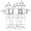
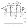
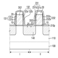
도 1은 본 발명의 몇몇 실시예에 따른 반도체 장치를 설명하기 위한 평면도이다.
도 2는 도 1의 A - A를 따라서 절단한 단면도이다.
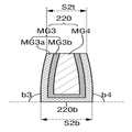
도 3은 도 2에서 제1 게이트 전극을 제외한 제1 게이트 스페이서를 도시한 도면이다.
도 4는 도 2에서, 제1 게이트 전극만을 분리하여 도시한 도면이다.
도 5는 도 2에서 제2 게이트 전극을 제외한 제2 게이트 스페이서를 도시한 도면이다.
도 6은 도 2에서, 제2 게이트 전극만을 분리하여 도시한 도면이다.
도 7a 내지 도 8b는 도 2의 B - B를 따라서 절단한 단면도이다.
도 9a 내지 도 10b는 도 2의 C - C를 따라서 절단한 단면도이다.
도 11은 본 발명의 몇몇 실시예에 따른 반도체 장치를 설명하기 위한 도면이다.
도 12는 본 발명의 몇몇 실시예에 따른 반도체 장치를 설명하기 위한 도면이다.
도 13은 본 발명의 몇몇 실시예에 따른 반도체 장치를 설명하기 위한 도면이다.
도 14 내지 19는 본 발명의 몇몇 실시예에 따른 반도체 장치 제조 방법을 설명하기 위한 중단 단계 도면들이다.
도 20은 본 발명의 몇몇 실시예에 따른 반도체 장치 제조 방법을 설명하기 위한 중간 단계의 도면이다.
도 21은 본 발명의 몇몇 실시예에 따른 반도체 장치 제조 방법을 설명하기 위한 중간 단계의 도면이다.
도 22 내지 도 26은 본 발명의 몇몇 실시예에 따른 반도체 장치 제조 방법을 설명하기 위한 중간 단계의 도면들이다.
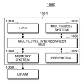
도 27은 본 발명의 실시예들에 따른 반도체 장치를 포함하는 SoC 시스템의 블록도이다.1 is a plan view for explaining a semiconductor device according to some embodiments of the present invention.
2 is a cross-sectional view taken along line A-A in Fig.
FIG. 3 is a view showing a first gate spacer excluding the first gate electrode in FIG. 2. FIG.
FIG. 4 is a view showing only the first gate electrode in FIG. 2; FIG.
5 is a view showing a second gate spacer except the second gate electrode in FIG.
FIG. 6 is a view showing only the second gate electrode in FIG. 2; FIG.
Figs. 7A to 8B are cross-sectional views taken along the line B-B in Fig.
9A to 10B are cross-sectional views taken along line C-C in Fig.
11 is a view for explaining a semiconductor device according to some embodiments of the present invention.
12 is a view for explaining a semiconductor device according to some embodiments of the present invention.
13 is a view for explaining a semiconductor device according to some embodiments of the present invention.
FIGS. 14 to 19 are diagrams for explaining the steps of the semiconductor device manufacturing method according to some embodiments of the present invention.
20 is a diagram of an intermediate step for explaining a method of manufacturing a semiconductor device according to some embodiments of the present invention.
21 is a diagram of an intermediate step for explaining a method of manufacturing a semiconductor device according to some embodiments of the present invention.
22 to 26 are diagrams of an intermediate step for explaining a semiconductor device manufacturing method according to some embodiments of the present invention.
27 is a block diagram of a SoC system including a semiconductor device according to embodiments of the present invention.
본 발명의 이점 및 특징, 그리고 그것들을 달성하는 방법은 첨부되는 도면과 함께 상세하게 후술되어 있는 실시예들을 참조하면 명확해질 것이다. 그러나 본 발명은 이하에서 개시되는 실시예들에 한정되는 것이 아니라 서로 다른 다양한 형태로 구현될 것이며, 단지 본 실시예들은 본 발명의 개시가 완전하도록 하며, 본 발명이 속하는 기술분야에서 통상의 지식을 가진 자에게 발명의 범주를 완전하게 알려주기 위해 제공되는 것이며, 본 발명은 청구항의 범주에 의해 정의될 뿐이다. 도면에서 층 및 영역들의 상대적인 크기는 설명의 명료성을 위해 과장된 것일 수 있다. 명세서 전체에 걸쳐 동일 참조 부호는 동일 구성 요소를 지칭한다. BRIEF DESCRIPTION OF THE DRAWINGS The advantages and features of the present invention, and the manner of achieving them, will be apparent from and elucidated with reference to the embodiments described hereinafter in conjunction with the accompanying drawings. The present invention may, however, be embodied in many different forms and should not be construed as being limited to the embodiments set forth herein. Rather, these embodiments are provided so that this disclosure will be thorough and complete, and will fully convey the scope of the invention to those skilled in the art. Is provided to fully convey the scope of the invention to those skilled in the art, and the invention is only defined by the scope of the claims. The relative sizes of layers and regions in the figures may be exaggerated for clarity of illustration. Like reference numerals refer to like elements throughout the specification.
하나의 소자(elements)가 다른 소자와 "접속된(connected to)" 또는 "커플링된(coupled to)" 이라고 지칭되는 것은, 다른 소자와 직접 연결 또는 커플링된 경우 또는 중간에 다른 소자를 개재한 경우를 모두 포함한다. 반면, 하나의 소자가 다른 소자와 "직접 접속된(directly connected to)" 또는 "직접 커플링된(directly coupled to)"으로 지칭되는 것은 중간에 다른 소자를 개재하지 않은 것을 나타낸다. One element is referred to as being "connected to " or" coupled to "another element, either directly connected or coupled to another element, One case. On the other hand, when one element is referred to as being "directly connected to" or "directly coupled to " another element, it does not intervene another element in the middle.
명세서 전체에 걸쳐 동일 참조 부호는 동일 구성 요소를 지칭한다. "및/또는"은 언급된 아이템들의 각각 및 하나 이상의 모든 조합을 포함한다. Like reference numerals refer to like elements throughout the specification. "And / or" include each and every combination of one or more of the mentioned items.
소자(elements) 또는 층이 다른 소자 또는 층의 "위(on)" 또는 "상(on)"으로 지칭되는 것은 다른 소자 또는 층의 바로 위뿐만 아니라 중간에 다른 층 또는 다른 소자를 개재한 경우를 모두 포함한다. 반면, 소자가 "직접 위(directly on)" 또는 "바로 위"로 지칭되는 것은 중간에 다른 소자 또는 층을 개재하지 않은 것을 나타낸다. It is to be understood that when an element or layer is referred to as being "on" or " on "of another element or layer, All included. On the other hand, a device being referred to as "directly on" or "directly above" indicates that no other device or layer is interposed in between.
비록 제1, 제2 등이 다양한 소자, 구성요소 및/또는 섹션들을 서술하기 위해서 사용되나, 이들 소자, 구성요소 및/또는 섹션들은 이들 용어에 의해 제한되지 않음은 물론이다. 이들 용어들은 단지 하나의 소자, 구성요소 또는 섹션들을 다른 소자, 구성요소 또는 섹션들과 구별하기 위하여 사용하는 것이다. 따라서, 이하에서 언급되는 제1 소자, 제1 구성요소 또는 제1 섹션은 본 발명의 기술적 사상 내에서 제2 소자, 제2 구성요소 또는 제2 섹션일 수도 있음은 물론이다. Although the first, second, etc. are used to describe various elements, components and / or sections, it is needless to say that these elements, components and / or sections are not limited by these terms. These terms are only used to distinguish one element, element or section from another element, element or section. Therefore, it goes without saying that the first element, the first element or the first section mentioned below may be the second element, the second element or the second section within the technical spirit of the present invention.
본 명세서에서 사용된 용어는 실시예들을 설명하기 위한 것이며 본 발명을 제한하고자 하는 것은 아니다. 본 명세서에서, 단수형은 문구에서 특별히 언급하지 않는 한 복수형도 포함한다. 명세서에서 사용되는 "포함한다(comprises)" 및/또는 "포함하는(comprising)"은 언급된 구성요소, 단계, 동작 및/또는 소자는 하나 이상의 다른 구성요소, 단계, 동작 및/또는 소자의 존재 또는 추가를 배제하지 않는다. The terminology used herein is for the purpose of illustrating embodiments and is not intended to be limiting of the present invention. In the present specification, the singular form includes plural forms unless otherwise specified in the specification. It is noted that the terms "comprises" and / or "comprising" used in the specification are intended to be inclusive in a manner similar to the components, steps, operations, and / Or additions.
다른 정의가 없다면, 본 명세서에서 사용되는 모든 용어(기술 및 과학적 용어를 포함)는 본 발명이 속하는 기술분야에서 통상의 지식을 가진 자에게 공통적으로 이해될 수 있는 의미로 사용될 수 있을 것이다. 또 일반적으로 사용되는 사전에 정의되어 있는 용어들은 명백하게 특별히 정의되어 있지 않는 한 이상적으로 또는 과도하게 해석되지 않는다.Unless defined otherwise, all terms (including technical and scientific terms) used herein may be used in a sense commonly understood by one of ordinary skill in the art to which this invention belongs. Also, commonly used predefined terms are not ideally or excessively interpreted unless explicitly defined otherwise.
이하, 도 1 내지 도 10a을 참조하여 본 발명의 일 실시예에 따른 반도체 장치를 설명한다.Hereinafter, a semiconductor device according to an embodiment of the present invention will be described with reference to FIGS. 1 to 10A.
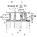
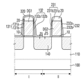
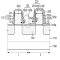
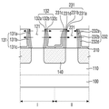
도 1은 본 발명의 몇몇 실시예에 따른 반도체 장치를 설명하기 위한 평면도이고, 도 2는 도 1의 A - A를 따라서 절단한 단면도이다. 도 3은 도 2에서 제1 게이트 전극을 제외한 제1 게이트 스페이서를 도시한 도면이고, 도 4는 도 2에서, 제1 게이트 전극만을 분리하여 도시한 도면이다. 도 5는 도 2에서 제2 게이트 전극을 제외한 제2 게이트 스페이서를 도시한 도면이고, 도 6은 도 2에서, 제2 게이트 전극만을 분리하여 도시한 도면이다. 도 7a 내지 도 8b는 도 2의 B - B를 따라서 절단한 단면도이고, 도 9a 내지 도 10b는 도 2의 C - C를 따라서 절단한 단면도이다.FIG. 1 is a plan view for explaining a semiconductor device according to some embodiments of the present invention, and FIG. 2 is a sectional view taken along line A - A in FIG. FIG. 3 is a view showing a first gate spacer except a first gate electrode in FIG. 2. FIG. 4 is a view showing only a first gate electrode in FIG. FIG. 5 is a view showing a second gate spacer except the second gate electrode in FIG. 2, and FIG. 6 is a view showing only the second gate electrode in FIG. Figs. 7A and 8B are cross-sectional views taken along B-B in Fig. 2, and Figs. 9A and 10B are cross-sectional views taken along C-C in Fig.
도면에서는 예시적으로, 반도체 장치는 핀형 패턴 형상의 채널 영역을 포함하는 것으로 도시하였지만, 핀형 패턴 형상 대신 와이어 패턴 형상의 채널 영역을 포함할 수도 있다.In the drawing, the semiconductor device is illustrated as including a channel region of a fin-shaped pattern shape, but it may also include a channel region of a wire pattern shape instead of a pin-shaped pattern shape.
또한, 이하에서는 반도체 장치는 핀형 패턴을 이용한 핀형 트랜지스터(FinFET)을 포함하는 것으로 설명하지만, 이에 제한되는 것은 아니다. 즉, 본 발명의 실시예들에 따른 반도체 장치는 평면(planar) 트랜지스터를 포함할 수 있음은 물론이다.In the following, the semiconductor device is described as including a fin-type transistor (FinFET) using a fin-shaped pattern, but the present invention is not limited thereto. That is, the semiconductor device according to embodiments of the present invention may include a planar transistor.
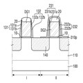
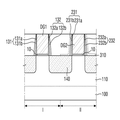
도 1 내지 도 4b를 참고하면, 본 발명의 몇몇 실시예에 따른 반도체 장치는 제1 핀형 패턴(110)과, 제1 게이트 전극(120)과, 제2 게이트 전극(220)과, 제1 게이트 스페이서(131, 132)와, 제2 게이트 스페이서(231, 232)와, 층간 절연막(180)을 포함할 수 있다.1 to 4B, a semiconductor device according to some embodiments of the present invention includes a
기판(100)은 예를 들어, 벌크 실리콘 또는 SOI(silicon-on-insulator)일 수 있다. 이와 달리, 기판(100)은 실리콘 기판일 수도 있고, 또는 다른 물질, 예를 들어, 실리콘게르마늄, 안티몬화 인듐, 납 텔루르 화합물, 인듐 비소, 인듐 인화물, 갈륨 비소 또는 안티몬화 갈륨을 포함할 수 있다. 또는, 기판(100)은 베이스 기판 상에 에피층이 형성된 것일 수도 있다.The
기판(100)은 제1 영역(Ⅰ) 및 제2 영역(Ⅱ)을 포함할 수 있다. 제1 영역(Ⅰ) 및 제2 영역(Ⅱ)은 서로 인접한 영역일 수 있다. 단, 이에 제한되는 것은 아니다. 제1 영역(Ⅰ)에는 추후에 설명되는 제1 게이트 전극(120)이 형성될 수 있고, 제2 영역(Ⅱ)에는 추후에 설명되는 제2 게이트 전극(220)이 형성될 수 있다.The
제1 핀형 패턴(110)은 기판(100)으로부터 돌출되어 있을 수 있다. 제1 핀형 패턴(110)은 제1 방향(X1)을 따라서 길게 연장될 수 있다.The first fin-shaped
제1 핀형 패턴(110)은 멀티 게이트 트랜지스터에 사용되는 액티브 패턴을 의미한다. 즉, 제1 핀형 패턴(110)은 핀의 3면을 따라서 채널이 서로 연결되어 형성될 수도 있고, 핀의 서로 마주보는 2면에 채널이 형성될 수도 있다.The first fin-shaped
제1 핀형 패턴(110)은 기판(100)의 일부일 수도 있고, 기판(100)으로부터 성장된 에피층(epitaxial layer)을 포함할 수 있다.The first pinned
제1 핀형 패턴(110)은 예를 들어, 원소 반도체 물질인 실리콘 또는 게르마늄을 포함할 수 있다. 또한, 제1 핀형 패턴(110)은 화합물 반도체를 포함할 수 있고, 예를 들어, IV-IV족 화합물 반도체 또는 III-V족 화합물 반도체를 포함할 수 있다.The
구체적으로, IV-IV족 화합물 반도체를 예로 들면, 제1 핀형 패턴(110)은 탄소(C), 규소(Si), 게르마늄(Ge), 주석(Sn) 중 적어도 2개 이상을 포함하는 이원계 화합물(binary compound), 삼원계 화합물(ternary compound) 또는 이들에 IV족 원소가 도핑된 화합물일 수 있다.Specifically, as an example of the IV-IV group compound semiconductor, the
III-V족 화합물 반도체를 예로 들면, 제1 핀형 패턴(110)은 III족 원소로 알루미늄(Al), 갈륨(Ga) 및 인듐(In) 중 적어도 하나와 V족 원소인 인(P), 비소(As) 및 안티모늄(Sb) 중 하나가 결합되어 형성되는 이원계 화합물, 삼원계 화합물 또는 사원계 화합물 중 하나일 수 있다.The
본 발명의 실시예들에 따른 반도체 장치에서, 제1 핀형 패턴(110)은 실리콘을 포함하는 실리콘 핀형 패턴인 것으로 설명한다.In the semiconductor device according to the embodiments of the present invention, the first
제1 필드 절연막(105)은 기판(100) 상에 형성될 수 있다. 제1 필드 절연막(105)은 제1 핀형 패턴(110)의 측면 일부를 덮고 있을 수 있다. 이에 따라, 제1 핀형 패턴(110)의 상면은 제1 핀형 패턴(110)의 장변 측에 배치되는 제1 필드 절연막(105)의 상면보다 위로 돌출되어 있을 수 있다. 제1 핀형 패턴(110)은 기판(100) 상의 제1 필드 절연막(105)에 의해 정의될 수 있다.The first
제1 필드 절연막(105)은 예를 들어, 산화막, 질화막, 산질화막 또는 이들의 조합 중 하나를 포함할 수 있다.The first
제1 게이트 전극(120)은 제2 방향(Y1)으로 연장될 수 있다. 제1 게이트 전극(120)은 제1 핀형 패턴(110)과 교차하도록 형성될 수 있다.The
제1 게이트 전극(120)은 제1 핀형 패턴(110) 및 제1 필드 절연막(105) 상에 형성될 수 있다. 제1 게이트 전극(120)은 제1 필드 절연막(105)의 상면보다 위로 돌출된 제1 핀형 패턴(110)을 감쌀 수 있다.The
제1 게이트 전극(120)은 서로 마주보는 제1 측벽(120a)과 제2 측벽(120c)을 포함할 수 있다. 제1 게이트 전극(120)은 제1 게이트 전극의 제1 측벽(120a) 및 제1 게이트 전극의 제2 측벽(120c)을 연결하고, 제1 핀형 패턴(110)의 상면을 따라 연장되는 바닥면(120b)를 포함할 수 있다.The
제2 게이트 전극(220)은 제2 방향(Y1)으로 연장될 수 있다. 제2 게이트 전극(220)은 제1 핀형 패턴(110) 상에, 제1 핀형 패턴(110)과 교차하도록 형성될 수 있다.The
제2 게이트 전극(220)은 제1 게이트 전극(120)에 인접하여 형성될 수 있다. 제2 게이트 전극(220)과 제1 게이트 전극(120) 사이에 제1 핀형 패턴(110) 교차하는 다른 게이트 전극은 형성되지 않을 수 있다.The
제2 게이트 전극(220)은 서로 마주보는 제1 측벽(220a)과 제2 측벽(220c)을 포함할 수 있다. 제2 게이트 전극(220)은 제2 게이트 전극의 제1 측벽(220a) 및 제2 게이트 전극의 제2 측벽(220c)을 연결하고, 제1 핀형 패턴(110)의 상면을 따라 연장되는 바닥면(220b)를 포함할 수 있다.The
제1 게이트 전극(120)은 금속층(MG1, MG2)을 포함할 수 있다. 예를 들어, 제1 게이트 전극(120)은 도시한 것과 같이, 2층 이상의 금속층(MG1, MG2)이 적층될 수 있다. 제1 금속층(MG1)은 일함수 조절을 하고, 제2 금속층(MG2)은 제1 금속층(MG1)에 의해 형성된 공간을 채우는 역할을 한다. 예를 들어, 제1 금속층(MG1)은 N형 일함수막일 수 있다. 제1 금속층(MG1)은 예를 들어, TiAl, TiAlN, TaC, TaAlN, TiC, HfSi 또는 이들의 조합 중 적어도 하나를 포함할 수 있지만, 이에 제한되는 것은 아니다. 또한, 제2 금속층(MG2)은 예를 들어, W, Al, Cu, Co, Ti, Ta, poly-Si, SiGe 또는 금속 합금 중 적어도 하나를 포함할 수 있지만, 이에 제한되는 것은 아니다. The
제2 게이트 전극(220)은 금속층(MG3, MG4)을 포함할 수 있다. 예를 들어, 제2 게이트 전극(220)은 도시한 것과 같이, 2층 이상의 금속층(MG3, MG4)이 적층될 수 있다. 제3 금속층(MG3)은 일함수 조절을 하고, 제4 금속층(MG4)은 제3 금속층(MG3)에 의해 형성된 공간을 채우는 역할을 한다. 제3 금속층(MG3)은 제1 서브 금속층(MG3a) 및 제2 서브 금속층(MG3b)을 포함할 수 있다. The
제1 서브 금속층(MG3a)은 N형 일함수막일 수 있다. 제1 금속층(MG1)은 예를 들어, TiAl, TiAlN, TaC, TaAlN, TiC, HfSi 또는 이들의 조합 중 적어도 하나를 포함할 수 있지만, 이에 제한되는 것은 아니다.The first sub-metal layer MG3a may be an N-type work function film. The first metal layer MG1 may include, but is not limited to, at least one of, for example, TiAl, TiAlN, TaC, TaAlN, TiC, HfSi, or combinations thereof.
제2 서브 금속층(MG3b)은 제1 서브 금속층(MG3a) 상에 형성될 수 있다. 제2 서브 금속층은 P형 일함수막일 수 있다. 제2 서브 금속층(MG3b)은 예를 들어, 메탈 질화물을 포함할 수 있다. 구체적으로, 본 발명의 몇몇 실시예에서, 제2 서브 금속층(MG3b)은 예를 들어, TiN, TaN 중 적어도 하나를 포함도록 구성될 수 있다. 더욱 구체적으로, 제2 서브 금속층(MG3b)은 예를 들어, TiN으로 이루어진 단일막, 또는 TiN 하부막과 TaN 상부막으로 이루어진 이중막 등으로 이루어질 수 있으나, 본 발명이 이에 제한되는 것은 아니다.The second sub-metal layer MG3b may be formed on the first sub-metal layer MG3a. The second sub-metal layer may be a P-type work function film. The second sub-metal layer MG3b may comprise, for example, a metal nitride. Specifically, in some embodiments of the present invention, the second sub-metal layer MG3b may be configured to include at least one of TiN, TaN, for example. More specifically, the second sub-metal layer MG3b may be composed of, for example, a single film made of TiN or a double film made of a TiN lower film and a TaN upper film, but the present invention is not limited thereto.
제1 게이트 전극(120) 및 제2 게이트 전극(220)은 각각 예를 들어, 리플레이스먼트 공정(replacement process)(또는 게이트 라스트 공정(gate last process))을 통해서 형성될 수 있으나, 이에 한정되는 것은 아니다.The
제1 게이트 스페이서(131, 132)는 제1 게이트 전극(120)의 측벽 상에 배치될 수 있다. 제1 게이트 스페이서(131, 132)는 제1 게이트 전극의 제1 측벽(120a) 상에 배치되는 제1 일측 스페이서(131)와, 제1 게이트 전극의 제2 측벽(120c) 상에 배치되는 제1 타측 스페이서(132)를 포함할 수 있다.The
제1 일측 스페이서(131) 및 제1 타측 스페이서(132)는 제1 트렌치(121)를 정의할 수 있다. 제1 트렌치의 제1 측벽(121a)은 제1 일측 스페이서(131)에 의해 정의되고, 제1 트렌치의 제2 측벽(121c)은 제1 타측 스페이서(132)에 의해 정의될 수 있다. 제1 트렌치의 바닥면(121b)은 제1 트렌치의 제1 측벽(121a) 및 제1 트렌치의 제2 측벽(121c)을 연결하여 정의될 수 있다.The
제1 게이트 스페이서(131, 132)는 하부(131b, 132b)와, 상부(131a, 132a)를 포함할 수 있다. 좀 더 구체적으로, 제1 일측 스페이서(131)는 하부(131b) 및 상부(131a)를 포함하고, 제1 타측 스페이서(132)는 하부(132b) 및 상부(132a)를 포함할 수 있다.The
제2 게이트 스페이서(231, 232)는 제2 게이트 전극(220)의 측벽 상에 배치될 수 있다. 제2 게이트 스페이서(231, 232)는 제2 게이트 전극의 제1 측벽(220a) 상에 배치되는 제2 일측 스페이서(231)와, 제2 게이트 전극의 제2 측벽(220c) 상에 배치되는 제2 타측 스페이서(232)를 포함할 수 있다.The
제2 일측 스페이서(231) 및 제2 타측 스페이서(232)는 제2 트렌치(221)를 정의할 수 있다.The second one-
제2 일측 스페이서(231)는 하부(231b) 및 상부(231a)를 포함하고, 제2 타측 스페이서(232)는 하부(232b) 및 상부(232a)를 포함할 수 있다.The second one
제1 게이트 전극(120)은 제1 게이트 스페이서(131, 132)에 의해 정의되는 제1 트렌치(121)를 채워 형성될 수 있다. 제2 게이트 전극(220)은 제2 게이트 스페이서(231, 232)에 의해 정의되는 제2 트렌치(221)를 채워 형성될 수 있다.The
제1 게이트 스페이서(131, 132)는 제1 질화 스페이서(131a, 132a) 및 제1 산화 스페이서(131b, 132b)를 포함할 수 있다. 제1 질화 스페이서(131a, 132a)는 제1 게이트 전극(120) 상에 형성되고, 제1 산화 스페이서(131b, 132b)는 제1 질화 스페이서(131a, 132a) 상에 형성될 수 있다.The
제2 게이트 스페이서(231, 232)는 제2 질화 스페이서(231a, 232a) 및 제2 산화 스페이서(231b, 232b)를 포함할 수 있다. 제2 질화 스페이서(231a, 232a)는 제2 게이트 전극(220) 상에 형성되고, 제2 산화 스페이서(231b, 232b)는 제2 질화 스페이서(231a, 232a) 상에 형성될 수 있다.The
제1 질화 스페이서(131a, 132a) 및 제2 질화 스페이서(231a, 232a)는 실리콘 질화물(SiN), 실리콘 산질화물(SiON), 실리콘 산탄질화물(SiOCN) 및 이들의 조합 중 적어도 하나를 포함할 수 있다. 단, 이에 제한되는 것은 아니다.The
제1 산화 스페이서(131b, 132b) 및 제2 산화 스페이서(231b, 232b)는 실리콘 산화물(SiO2)을 포함할 수 있다. 단, 이에 제한되는 것은 아니다.The
제1 게이트 절연막(125)은 제1 핀형 패턴(110)과 제1 게이트 전극(120) 사이에 형성될 수 있다. 제1 게이트 절연막(125)은 제1 필드 절연막(105)보다 위로 돌출된 제1 핀형 패턴(110)의 프로파일을 따라 형성될 수 있다.The first
제1 게이트 절연막(125)은 제1 게이트 전극(120)과 제1 필드 절연막(105) 사이에 배치될 수 있다. 제1 게이트 절연막(125)은 제1 트렌치(121)의 측벽 및 바닥면을 따라 형성될 수 있다. 제1 게이트 절연막(125)은 제1 게이트 스페이서(131, 132)와 제1 게이트 전극(120) 사이에 형성될 수 있다.The first
덧붙여, 제1 게이트 절연막(125) 및 제1 핀형 패턴(110) 사이에, 계면막(interfacial layer)(126)이 더 형성될 수 있다. 도시되지 않았지만, 도 2에서도, 제1 게이트 절연막(125) 및 제1 핀형 패턴(110) 사이에 계면막이 더 형성될 수 있다.In addition, an
도 8a, 도 8b, 도 10a 및 도 10b에서, 계면막(121)이 제1 필드 절연막(105)의 상면보다 돌출된 제1 핀형 패턴(110)의 프로파일을 따라서 형성되는 것으로 도시하였지만, 이에 제한되는 것은 아니다.8A, 8B, 10A, and 10B, the
도 7b, 도 8b, 도 9b 및 도 10b에서 제1 필드 절연막(105)에 의해 덮인 제1 핀형 패턴(110)의 측벽은 기판(100)의 상면에 대해 예각의 기울기를 가질 수 있다. 제1 필드 절연막(105)에 의해 덮인 제1 핀형 패턴(110)의 폭은 기판(100)의 상면으로부터 멀어짐에 따라 감소할 수 있다. The sidewalls of the
제1 필드 절연막(105)에 의해 덮인 제1 핀형 패턴(110)의 폭이 기판(100)의 상면으로부터 멀어짐에 따라 감소할 경우, 제1 핀형 패턴(110) 하부로의 누설 전류가 감소될 수 있다.When the width of the first
계면막(121)을 형성하는 방법에 따라, 계면막(121)은 제1 필드 절연막(105)의 상면을 따라서 연장될 수도 있다. Depending on the method of forming the
이하에서는, 설명의 편의성을 위해, 계면막(121)을 도시하지 않은 도면을 이용하여 설명한다.Hereinafter, for convenience of explanation, the
제2 게이트 절연막(225)은 제1 핀형 패턴(110)과 제2 게이트 전극(220) 사이에 형성될 수 있다. 제2 게이트 절연막(225)은 제2 트렌치(221)의 측벽 및 바닥면을 따라 형성될 수 있다. 제2 게이트 절연막(225)은 제2 게이트 스페이서(231, 232)와 제2 게이트 전극(220) 사이에 형성될 수 있다. 제2 게이트 절연막(225)에 관한 설명은 제1 게이트 절연막(125)에 관한 설명과 유사할 수 있다.The second
제1 게이트 절연막(125) 및 제2 게이트 절연막(225)은 실리콘 산화막보다 높은 유전 상수를 갖는 고유전체 물질을 포함할 수 있다. 예를 들어, 제1 게이트 절연막(125) 및 제2 게이트 절연막(225)은 각각 하프늄 산화물(hafnium oxide), 하프늄 실리콘 산화물(hafnium silicon oxide), 란타늄 산화물(lanthanum oxide), 란타늄 알루미늄 산화물(lanthanum aluminum oxide), 지르코늄 산화물(zirconium oxide), 지르코늄 실리콘 산화물(zirconium silicon oxide), 탄탈륨 산화물(tantalum oxide), 티타늄 산화물(titanium oxide), 바륨 스트론튬 티타늄 산화물(barium strontium titanium oxide), 바륨 티타늄 산화물(barium titanium oxide), 스트론튬 티타늄 산화물(strontium titanium oxide), 이트륨 산화물(yttrium oxide), 알루미늄 산화물(Aluminum oxide), 납 스칸듐 탄탈륨 산화물(lead scandium tantalum oxide), 또는 납 아연 니오브산염(lead zinc niobate) 중에서 하나 이상을 포함할 수 있으나, 이에 제한되는 것은 아니다.The first
제1 소오스/드레인 영역(140)은 제1 게이트 전극(120)의 양측 및 제2 게이트 전극(220)의 양측에 형성될 수 있다. The first source /
제1 소오스/드레인 영역(140)은 제1 핀형 패턴(110) 내에 형성된 불순물 영역으로 도시하였지만, 이에 제한되는 것은 아니다, 제1 소오스/드레인 영역(140)은 제1 핀형 패턴(110) 상 또는 제1 핀형 패턴(110) 내에 형성된 에피택셜층을 포함할 수 있다.The first source /
또한, 제1 소오스/드레인 영역(140)은 제1 핀형 패턴(110)의 상면보다 위로 돌출된 상면을 포함하는 상승된 소오스/드레인 영역일 수도 있다.The first source /
층간 절연막(180)은 기판(100) 상에 형성될 수 있다. 층간 절연막(180)은 제1 핀형 패턴(110)과, 제1 소오스/드레인 영역(140)과, 제1 필드 절연막(105)을 덮을 수 있다. An interlayer insulating
층간 절연막(180)은 제1 게이트 전극(120) 및 제2 게이트 전극(220)의 측벽을 감쌀 수 있다. 좀 더 구체적으로, 층간 절연막(180)은 제1 게이트 스페이서(131, 132)의 외측벽 및 제2 게이트 스페이서(231, 232)의 외측벽을 감쌀 수 있다.The interlayer insulating
도 2에서, 제1 게이트 전극(120)의 상면 및 제2 게이트 전극(220)의 상면은 상부 층간 절연막(182)의 상면과 동일 평면 상에 놓이는 것으로 도시하였지만, 이에 제한되는 것은 아니다.2, the upper surface of the
예를 들어, 자기 정렬 컨택(Self Aligned Contact, SAC) 구조를 형성하기 위해, 제1 게이트 전극(120) 및 제2 게이트 전극(220)의 상면 상에 각각 캡핑 패턴이 형성될 경우, 제1 게이트 전극(120)의 상면 및 제2 게이트 전극(220)의 상면은 층간 절연막(180)의 상면보다 낮을 수 있다.For example, when a capping pattern is formed on the upper surfaces of the
층간 절연막(180)은 예를 들어, 실리콘 산화물, 실리콘 산질화물, 실리콘 질화물, FOX(Flowable Oxide), TOSZ(Tonen SilaZen), USG(Undoped Silica Glass), BSG(Borosilica Glass), PSG(PhosphoSilica Glass), BPSG(BoroPhosphoSilica Glass), PETEOS(Plasma Enhanced Tetra Ethyl Ortho Silicate), FSG(Fluoride Silicate Glass), CDO(Carbon Doped silicon Oxide), Xerogel, Aerogel, Amorphous Fluorinated Carbon, OSG(Organo Silicate Glass), Parylene, BCB(bis-benzocyclobutenes), SiLK, polyimide, porous polymeric material 또는 이들의 조합을 포함할 수 있으나, 이에 제한되는 것은 아니다.The
기판(100)으로부터 층간 절연막(180)의 상면까지의 높이는 기판(100)으로부터 제1 게이트 스페이서(131, 132)의 최상부까지의 높이와 실질적으로 동일할 수 있다.The height from the
도 2 및 도 3에서, 제1 일측 스페이서(131)에 의해 정의되는 제1 트렌치의 제1 측벽(121a)은 제1 트렌치의 바닥면(121b)에 대해 제1 각도(a1)의 기울기를 가질 수 있다. 제1 타측 스페이서(132)에 의해 정의되는 제1 트렌치의 제2 측벽(121c)은 제1 트렌치의 바닥면(121b)에 대해 제2 각도(a2)의 기울기를 가질 수 있다.2 and 3, the
제1 각도(a1) 및 제2 각도(a2)는 직각보다 큰 둔각일 수 있다. 기판(100)의 상면 즉, 제1 트렌치의 바닥면(121b)으로부터 멀어짐에 따라, 제1 트렌치(121)의 폭은 증가할 수 있다.The first angle a1 and the second angle a2 may be obtuse angles greater than orthogonal. The width of the
도 3에서 도시된 것과 같이, 제1 트렌치의 바닥면(121b)에 대해, 제1 트렌치의 제1 측벽(121a) 및 제1 트렌치의 제2 측벽(121c)이 각각 둔각인 기울기를 가질 경우, 층간 절연막(180) 및 제1 게이트 스페이서(131, 132)의 인장 응력(tensile stress)의 크기가 압축 응력(compressive stress)의 크기보다 클 수 있다.As shown in Fig. 3, when the
여기서, "인장 응력 "이라 함은 층간 절연막 또는 스페이서가 게이트 전극을 층간 절연막 또는 스페이서 쪽으로 당기는 응력을 가지고 있다는 것을 의미하고, "압축 응력 "이라 함은 층간 절연막 또는 스페이서가 게이트 전극을 게이트 전극 쪽으로 미는 응력을 가지고 있다는 것을 의미한다. Here, the term "tensile stress" means that the interlayer insulating film or spacer has a stress that pulls the gate electrode toward the interlayer insulating film or the spacer, and the term "compressive stress" means that the interlayer insulating film or spacer It means that it has stress.
도 2 및 도 4에서, 제1 게이트 전극의 제1 측벽(120a)은 제1 게이트 전극의 바닥면(120b)에 대해 제3 각도(b1)의 기울기를 가질 수 있다. 제1 게이트 전극의 제2 측벽(120c)은 제1 게이트 전극의 바닥면(120b)에 대해 제4 각도(b2)의 기울기를 가질 수 있다.2 and 4, the
제1 게이트 전극의 제1 측벽(120a)은 제1 일측 스페이서(131)의 측벽과 마주하고, 제1 게이트 전극의 제2 측벽(120c)은 제1 타측 스페이서(132)의 측벽과 마주하므로, 제3 각도(b1) 및 제4 각도(b2)는 제1 각도(a1) 및 제2 각도(a2)와 마찬가지로 직각보다 큰 둔각일 수 있다.The
기판(100)의 상면으로부터 멀어짐에 따라, 제1 게이트 전극(120)의 폭은 증가할 수 있다. 다시 말하면, 제1 게이트 전극의 바닥면(120b)으로부터 제1 게이트 전극(120)의 상면까지 이동함에 따라, 제1 게이트 전극(120)의 폭은 증가할 수 있다.As the distance from the top surface of the
도시된 것과 달리, 제1 게이트 전극의 제1 측벽(120a) 및 제1 게이트 전극의 바닥면(120b)이 만나는 지점과, 제1 게이트 전극의 제2 측벽(120c) 및 제1 게이트 전극의 바닥면(120b)이 만나는 지점이 라운딩된 형상을 가지고 있다고 하여도, 본 발명이 속하는 당업자가 제1 게이트 전극의 제1 측벽(120a)의 기울기 및 제1 게이트 전극의 제2 측벽(120c)의 기울기를 구할 수 있음은 자명하다.A portion where the
제1 게이트 전극의 하면의 폭(S1b)에 대한 제1 게이트 전극의 상면의 폭(S1t)의 비율은 1보다 클 수 있다. 즉, 제1 게이트 전극의 하면의 폭(S1b)은 제1 게이트 전극의 상면의 폭(S1t)보다 작을 수 있다.The ratio of the width S1t of the upper surface of the first gate electrode to the width S1b of the lower surface of the first gate electrode may be larger than 1. [ That is, the width S1b of the lower surface of the first gate electrode may be smaller than the width S1t of the upper surface of the first gate electrode.
도 2 및 도 5에서, 제2 일측 스페이서(231)에 의해 정의되는 제2 트렌치의 제1 측벽(221a)은 제2 트렌치의 바닥면(221b)에 대해 제5 각도(a3)의 기울기를 가질 수 있다. 제2 타측 스페이서(232)에 의해 정의되는 제2 트렌치의 제2 측벽(221c)은 제2 트렌치의 바닥면(221b)에 대해 제6 각도(a4)의 기울기를 가질 수 있다.2 and 5, the
제5 각도(a3) 및 제6 각도(a4)는 직각보다 작은 예각일 수 있다. 기판(100)의 상면 즉, 제2 트렌치의 바닥면(221b)으로부터 멀어짐에 따라, 제2 트렌치(221)의 폭은 감소할 수 있다.The fifth angle a3 and the sixth angle a4 may be acute angles smaller than a right angle. The width of the
도 5에서 도시된 것과 같이, 제2 트렌치의 바닥면(221b)에 대해, 제2 트렌치의 제1 측벽(221a) 및 제2 트렌치의 제2 측벽(221c)이 각각 예각인 기울기를 가질 경우, 층간 절연막(180) 및 제2 게이트 스페이서(231, 232)의 압축 응력의 크기가 인장 응력의 크기보다 클 수 있다.As shown in Fig. 5, when the
도 2 및 도 6에서, 제2 게이트 전극의 제1 측벽(220a)은 제2 게이트 전극의 바닥면(220b)에 대해 제7 각도(b3)의 기울기를 가질 수 있다. 제2 게이트 전극의 제2 측벽(220c)은 제2 게이트 전극의 바닥면(220b)에 대해 제8 각도(b4)의 기울기를 가질 수 있다.2 and 6, the first sidewall 220a of the second gate electrode may have a slope of the seventh angle b3 relative to the
제2 게이트 전극의 제1 측벽(220a)은 제2 일측 스페이서(231)의 측벽과 마주하고, 제2 게이트 전극의 제2 측벽(220c)은 제2 타측 스페이서(232)의 측벽과 마주하므로, 제7 각도(b3) 및 제8 각도(b4)는 제5 각도(a3) 및 제6 각도(a4)와 마찬가지로 직각보다 작은 예각일 수 있다.The first sidewall 220a of the second gate electrode faces the sidewall of the second one
기판(100)의 상면으로부터 멀어짐에 따라, 제2 게이트 전극(220)의 폭은 감소할 수 있다. 다시 말하면, 제2 게이트 전극의 바닥면(220b)으로부터 제2 게이트 전극(220)의 상면까지 이동함에 따라, 제2 게이트 전극(220)의 폭은 증가할 수 있다.As the distance from the top surface of the
도시된 것과 달리, 제2 게이트 전극의 제1 측벽(220a) 및 제2 게이트 전극의 바닥면(220b)이 만나는 지점과, 제2 게이트 전극의 제2 측벽(220c) 및 제2 게이트 전극의 바닥면(220b)이 만나는 지점이 라운딩된 형상을 가지고 있다고 하여도, 본 발명이 속하는 당업자가 제2 게이트 전극의 제1 측벽(220a)의 기울기 및 제2 게이트 전극의 제2 측벽(220c)의 기울기를 구할 수 있음은 자명하다.A portion where the first sidewall 220a of the second gate electrode and the
제2 게이트 전극의 하면의 폭(S2b)에 대한 제2 게이트 전극의 상면의 폭(S2t)의 비율은 1보다 작을 수 있다. 즉, 제2 게이트 전극의 하면의 폭(S2b)은 제2 게이트 전극의 상면의 폭(S2t)보다 클 수 있다.The ratio of the width S2t of the upper surface of the second gate electrode to the width S2b of the lower surface of the second gate electrode may be smaller than 1. That is, the width S2b of the lower surface of the second gate electrode may be larger than the width S2t of the upper surface of the second gate electrode.
이하의 설명에서, 트렌치의 측벽이 트렌치의 바닥면에 대해 둔각의 기울기를 가질 경우, 트렌치의 측벽은 양의 기울기를 갖는 것으로 정의한다. 마찬가지로, 게이트 전극의 측벽이 게이트 전극의 바닥면에 대해 둔각의 기울기를 가질 경우, 게이트 전극의 측벽은 양의 기울기를 갖는 것으로 정의한다.In the following description, when the sidewall of the trench has an obtuse slope with respect to the bottom surface of the trench, the sidewall of the trench is defined as having a positive slope. Likewise, when the side wall of the gate electrode has an obtuse slope with respect to the bottom surface of the gate electrode, the side wall of the gate electrode is defined as having a positive slope.
반대로, 트렌치의 측벽이 트렌치의 바닥면에 대해 예각의 기울기를 가질 경우, 트렌치의 측벽은 음의 기울기를 갖는 것으로 정의한다. 마찬가지로, 게이트 전극의 측벽이 게이트 전극의 바닥면에 대해 예각의 기울기를 가질 경우, 게이트 전극의 측벽은 음의 기울기를 갖는 것으로 정의한다.Conversely, when the sidewalls of the trench have an acute slope with respect to the bottom surface of the trench, the sidewalls of the trench are defined as having a negative slope. Likewise, when the side wall of the gate electrode has an acute angle of inclination with respect to the bottom surface of the gate electrode, the side wall of the gate electrode is defined as having a negative slope.
즉, 도 2에서, 제1 게이트 전극의 제1 측벽(120a)과, 제1 게이트 전극의 제2 측벽(120c)은 양의 기울기를 가질 수 있다. 또한, 제2 게이트 전극의 제1 측벽(220a)과, 제2 게이트 전극의 제2 측벽(220c)은 음의 기울기를 가질 수 있다.That is, in FIG. 2, the
도 2에서는 제1 게이트 전극의 하면의 폭(S1b)에 대한 제1 게이트 전극의 상면의 폭(S1t)의 비율은 1보다 크고, 제2 게이트 전극의 하면의 폭(S2b)에 대한 제2 게이트 전극의 상면의 폭(S2t)의 비율은 1보다 작은 것으로 도시되었다. 다만, 본 발명의 다른 몇몇 실시예에서는 제1 게이트 전극의 하면의 폭(S1b)에 대한 제1 게이트 전극의 상면의 폭(S1t)과 제2 게이트 전극의 하면의 폭(S2b)에 대한 제2 게이트 전극의 상면의 폭(S2t)이 모두 1보다 작거나, 모두 1보다 클 수 있다. 단, 이러한 경우에도, 제1 게이트 전극의 하면의 폭(S1b)에 대한 제1 게이트 전극의 상면의 폭(S1t)의 비율은, 제2 게이트 전극의 하면의 폭(S2b)에 대한 제2 게이트 전극의 상면의 폭(S2t)의 비율보다 클 수 있다.2, the ratio of the width S1t of the upper surface of the first gate electrode to the width S1b of the lower surface of the first gate electrode is larger than 1, and the ratio of the width S2t of the second gate The ratio of the width S2t of the top surface of the electrode is shown to be less than one. However, in some other embodiments of the present invention, the width (S1t) of the upper surface of the first gate electrode and the width (S2b) of the lower surface of the second gate electrode with respect to the lower surface width (S1b) The width S2t of the upper surface of the gate electrode may be less than 1 or both may be larger than 1. [ In this case, the ratio of the width S1t of the upper surface of the first gate electrode to the width S1b of the lower surface of the first gate electrode is larger than the width S2t of the lower surface of the second gate electrode, May be larger than the ratio of the width S2t of the upper surface of the electrode.
본 발명의 몇몇 실시예에 따른 반도체 장치는 층간 절연막(180)의 밀도가 낮아서 식각 공정에서의 식각율(etch rate)가 높아지는 현상에 따른 공정의 난이도의 상승을 완화시킬 수 있다. 또한, PMOS 반도체 장치와 NMOS 반도체 장치에 각각 압축 응력과 인장 응력을 인가함으로서 반도체 장치의 성능을 향상시킬 수 있다.The semiconductor device according to some embodiments of the present invention has a low density of the interlayer insulating
구체적으로, 트랜지스터에 흐르는 유효 전류에 따라 누설 전류도 증가할 수 밖에 없지만, 상기 압축 응력과 인장 응력을 통해서, 유효 전류의 상승에 따른 누설 전류의 증가량이 줄어들 수 있다. 이에 따라 반도체 장치의 성능이 비약적으로 상승할 수 있다.Specifically, the leakage current also increases according to the effective current flowing through the transistor. However, the amount of increase of the leakage current due to the increase of the effective current can be reduced through the compressive stress and the tensile stress. As a result, the performance of the semiconductor device can dramatically increase.
도 11은 본 발명의 몇몇 실시예에 따른 반도체 장치를 설명하기 위한 도면이다. 설명의 편의상, 도 1 내지 도 10a을 이용하여 설명한 것과 다른 점을 중심으로 설명한다. 11 is a view for explaining a semiconductor device according to some embodiments of the present invention. For convenience of explanation, the differences from the one described with reference to Figs. 1 to 10A will be mainly described.
참고적으로, 도 11은 도 1의 A - A를 따라서 절단한 단면도이다.For reference, FIG. 11 is a cross-sectional view taken along line A-A in FIG.
도 11을 참고하면, 본 발명의 몇몇 실시예에 따른 반도체 장치에서, 제1 게이트 스페이서(131, 132)는 제1 스트레스 스페이서(131c, 132c)를 포함할 수 있다.Referring to FIG. 11, in a semiconductor device according to some embodiments of the present invention, the
제1 스트레스 스페이서(131c, 132c)는 제1 산화 스페이서(131b, 132b) 상에 형성될 수 있다. 제1 스트레스 스페이서(131c, 132c)는 제2 산화 스페이서(231b, 232b) 상에 형성되지 않는다. 제1 스트레스 스페이서(131c, 132c)는 제2 산화 스페이서(231b, 232b) 상에서 컨포말하게 형성될 수 있다. 나아가, 도시된 바와 같이 제1 스트레스 스페이서(131c, 132c)는 제1 소오스/드레인 영역(140)의 상면을 따라 형성될 수 있다. 단, 제1 스트레스 스페이서(131c, 132c)의 제1 소오스/드레인 영역(140)의 상면을 따라 형성된 부분은 본 발명의 몇몇 실시예에서는 존재하지 않을 수도 있다.The
제1 스트레스 스페이서(131c, 132c)는 제1 게이트 전극(120)에 인장 응력을 부가할 수 있다. 즉, 제1 게이트 전극(120)은 제1 스트레스 스페이서(131c, 132c)의 인장 응력에 따라 측벽에 양의 기울기를 가지는 형상을 가질 수 있다.The
제1 스트레스 스페이서(131c, 132c)는 예를 들어, 실리콘 질화막을 포함할 수 있으나, 이에 제한되는 것은 아니다.The
제2 게이트 스페이서(231, 232)는 제2 압축 스트레스 스페이서(231d, 232d)를 포함할 수 있다.The
제2 압축 스트레스 스페이서(231d, 232d)는 제2 산화 스페이서(231b, 232b) 상에 형성될 수 있다. 제2 압축 스트레스 스페이서(231d, 232d)는 제1 산화 스페이서(131b, 132b) 상에 형성되지 않는다. 제2 압축 스트레스 스페이서(231d, 232d)는 제2 산화 스페이서(231b, 232b) 상에서 컨포말하게 형성될 수 있다. 나아가, 도시된 바와 같이 제2 압축 스트레스 스페이서(231d, 232d)는 제1 소오스/드레인 영역(140)의 상면을 따라 형성될 수 있다. 단, 제2 압축 스트레스 스페이서(231d, 232d)의 제1 소오스/드레인 영역(140)의 상면을 따라 형성된 부분은 본 발명의 몇몇 실시예에서는 존재하지 않을 수도 있다.Second
제2 압축 스트레스 스페이서(231d, 232d)는 제2 게이트 전극(220)에 압축 응력을 부가할 수 있다. 즉, 제2 게이트 전극(220)은 제2 압축 스트레스 스페이서(231d, 232d)의 압축 응력에 따라 측벽에 음의 기울기를 가지는 형상을 가질 수 있다.The second
제2 압축 스트레스 스페이서(231d, 232d)는 예를 들어, 실리콘 산화막을 포함할 수 있으나, 이에 제한되는 것은 아니다. 제2 압축 스트레스 스페이서(231d, 232d)는 층간 절연막(180)과 동일한 물질을 포함할 수 있다. 이에 따라, 도 11에서는 제2 압축 스트레스 스페이서(231d, 232d)를 점선으로 표시하였다. 즉, 제2 압축 스트레스 스페이서(231d, 232d)는 층간 절연막(180)과 서로 구별되지 않을 수 있다.The second
도 12는 본 발명의 몇몇 실시예에 따른 반도체 장치를 설명하기 위한 도면이다. 설명의 편의상, 도 1 내지 도 11을 이용하여 설명한 것과 다른 점을 중심으로 설명한다. 12 is a view for explaining a semiconductor device according to some embodiments of the present invention. For convenience of explanation, the description will be focused on differences from those described with reference to Figs. 1 to 11. Fig.
참고적으로, 도 12는 도 1의 A - A를 따라서 절단한 단면도이다.For reference, FIG. 12 is a sectional view taken along the line A - A in FIG.
도 12를 참고하면, 본 발명의 몇몇 실시예에 따른 반도체 장치에서, 제1 게이트 스페이서(131, 132)는 제1 스트레스 스페이서(131c, 132c)를 포함할 수 있고, 제2 게이트 스페이서(231, 232)는 제2 스트레스 스페이서(231c, 232c)를 포함할 수 있다.12, in a semiconductor device according to some embodiments of the present invention, the
제1 스트레스 스페이서(131c, 132c)는 제1 산화 스페이서(131b, 132b) 상에 형성될 수 있다. 제2 스트레스 스페이서(231c, 232c)는 제2 산화 스페이서(231b, 232b) 상에 형성될 수 있다. 제1 스트레스 스페이서(131c, 132c)의 두께(T1, T3)는 제2 스트레스 스페이서(T2, T4)보다 두꺼울 수 있다.The
제1 스트레스 스페이서(131c, 132c)는 제2 스트레스 스페이서(231c, 232c)와 서로 연결될 수 있다. 구체적으로, 제1 스트레스 스페이서(132c)와 제2 스트레스 스페이서(231c)는 서로 연결될 수 있다. 제1 스트레스 스페이서(131c, 132c)는 제2 스트레스 스페이서(231c, 232c)는 서로 두께가 다르므로 제1 스트레스 스페이서(131c, 132c)는 제2 스트레스 스페이서(231c, 232c)가 연결되는 부분에 두께 단차가 형성될 수 있다. 상기 "두께 단차"란 두께가 서로 다른 양측이 만나는 부분으로 정의될 수 있다.The
제1 스트레스 스페이서(131c, 132c)와 제2 스트레스 스페이서(231c, 232c)는 각각 제1 게이트 전극(120)과 제2 게이트 전극(220)에 인장 응력을 부가할 수 있다. 다만, 제1 스트레스 스페이서(131c, 132c)와 제2 스트레스 스페이서(231c, 232c)의 두께가 서로 다르므로 제1 게이트 전극(120)에 가해지는 인장 응력은 제2 게이트 전극(220)에 가해지는 인장 응력보다 클 수 있다.The
이에 따라, 제1 게이트 전극의 하면의 폭(S1b)에 대한 제1 게이트 전극의 상면의 폭(S1t)의 비율은, 제2 게이트 전극의 하면의 폭(S2b)에 대한 제2 게이트 전극의 상면의 폭(S2t)의 비율보다 클 수 있다. 도 12에서는 제2 게이트 전극의 하면의 폭(S2b)에 대한 제2 게이트 전극의 상면의 폭(S2t)의 비율이 1보다 작은 경우로 도시되었으나, 이에 제한되는 것은 아니다. 제2 게이트 전극의 하면의 폭(S2b)에 대한 제2 게이트 전극의 상면의 폭(S2t)의 비율이 1보다 작은 경우에는 층간 절연막(180)에 의해서 제2 게이트 전극(220)에 압축 응력이 가해질 수 있다.As a result, the ratio of the width S1t of the upper surface of the first gate electrode to the width S1b of the lower surface of the first gate electrode is larger than the width S2b of the lower surface of the second gate electrode, Of the width S2t. In FIG. 12, the ratio of the width S2t of the upper surface of the second gate electrode to the width S2b of the lower surface of the second gate electrode is shown to be smaller than 1, however, the present invention is not limited thereto. When the ratio of the width S2t of the upper surface of the second gate electrode to the width S2b of the lower surface of the second gate electrode is smaller than 1, the compressive stress is applied to the
도 13은 본 발명의 몇몇 실시예에 따른 반도체 장치를 설명하기 위한 도면이다. 설명의 편의상, 도 1 내지 도 12를 이용하여 설명한 것과 다른 점을 중심으로 설명한다. 13 is a view for explaining a semiconductor device according to some embodiments of the present invention. For convenience of explanation, differences from those described with reference to Figs. 1 to 12 will be mainly described.
참고적으로, 도 13은 도 1의 A - A를 따라서 절단한 단면도이다.For reference, FIG. 13 is a sectional view taken along the line A - A in FIG.
도 13을 참고하면, 본 발명의 몇몇 실시예에 따른 반도체 장치에서, 제2 게이트 스페이서(231, 232)는 제1 스트레스 스페이서(131c, 132c)를 포함할 수 있고, 제2 게이트 스페이서(231, 232)는 제2 스트레스 스페이서(231c, 232c)와 제2 압축 스트레스 스페이서(231d, 232d)를 포함할 수 있다.13, in a semiconductor device according to some embodiments of the present invention, the
제2 압축 스트레스 스페이서(231d, 232d)는 제2 스트레스 스페이서(231c, 232c)와 제2 산화 스페이서(231b, 232b) 사이에 형성될 수 있다. 제2 압축 스트레스 스페이서(231d, 232d)는 제2 산화 스페이서(231b, 232b) 상에서 컨포말하게 형성될 수 있다. 나아가, 도시된 바와 같이 제2 압축 스트레스 스페이서(231d, 232d)는 제1 소오스/드레인 영역(140)의 상면을 따라 형성될 수 있다. 단, 제2 압축 스트레스 스페이서(231d, 232d)의 제1 소오스/드레인 영역(140)의 상면을 따라 형성된 부분은 본 발명의 몇몇 실시예에서는 존재하지 않을 수도 있다.Second
제2 압축 스트레스 스페이서(231d, 232d)는 제2 게이트 전극(220)에 압축 응력을 부가할 수 있다. 즉, 제2 게이트 전극(220)은 제2 압축 스트레스 스페이서(231d, 232d)의 압축 응력에 따라 측벽에 음의 기울기를 가지는 형상을 가질 수 있다.The second
제2 압축 스트레스 스페이서(231d, 232d)는 제2 산화 스페이서(231b, 232b)와 동일한 물질을 포함할 수 있다. 즉, 제2 압축 스트레스 스페이서(231d, 232d)는 예를 들어, 실리콘 산화물을 포함할 수 있다. 따라서, 제2 압축 스트레스 스페이서(231d, 232d)와 제2 산화 스페이서(231b, 232b)를 합쳐서 제3 산화 스페이서(231b', 232b')로 정의할 수 있다.The second
제1 산화 스페이서(131b, 132b)의 두께(G1)는 제3 산화 스페이서(231b', 232b')의 두께(G2)보다 작을 수 있다. 즉, 제1 산화 스페이서(131b, 132b)와 제2 산화 스페이서(231b, 232b)의 두께는 동일 내지 유사할 수 있으나, 제2 압축 스트레스 스페이서(231d, 232d)가 추가된 제3 산화 스페이서(231b', 232b')의 두께는 이보다 더 두꺼울 수 있다.The thickness G1 of the
제1 스트레스 스페이서(131c, 132c)는 제2 스트레스 스페이서(231c, 232c)와 서로 연결될 수 있다. 구체적으로, 제1 스트레스 스페이서(132c)와 제2 스트레스 스페이서(231c)는 서로 연결될 수 있다. The
제1 스트레스 스페이서(131c, 132c)는 제1 소오스/드레인 영역(140) 상에 바로 형성될 수 있다. 이에 반해, 제2 스트레스 스페이서(231c, 232c)는 제1 소오스/드레인 영역(140) 상에 위치한 제2 압축 스트레스 스페이서(231d, 232d) 상에 형성될 수 있다. 이에 따라, 제1 스트레스 스페이서(131c, 132c)와 제2 스트레스 스페이서(231c, 232c)가 만나는 지점에 높이 단차가 형성될 수 있다. 상기 "높이 단차"는 서로 상면의 높이가 다른 양측이 만나는 지점으로 정의할 수 있다.The
제1 스트레스 스페이서(131c, 132c)와 제2 스트레스 스페이서(231c, 232c)는 각각 제1 게이트 전극(120)과 제2 게이트 전극(220)에 인장 응력을 부가할 수 있다. 다만, 제2 압축 스트레스 스페이서(231d, 232d)가 제2 게이트 전극(220)에 압축 응력을 가하므로, 제1 게이트 전극(120)에 가해지는 총 인장 응력은 제2 게이트 전극(220)에 가해지는 총 인장 응력보다 클 수 있다. 반대로, 제1 게이트 전극(120)에 가해지는 총 압축 응력은 제2 게이트 전극(220)에 가해지는 총 압축 응력보다 작을 수 있다.The
이에 따라, 제1 게이트 전극의 하면의 폭(S1b)에 대한 제1 게이트 전극의 상면의 폭(S1t)의 비율은, 제2 게이트 전극의 하면의 폭(S2b)에 대한 제2 게이트 전극의 상면의 폭(S2t)의 비율보다 클 수 있다. 도 12에서는 제2 게이트 전극의 하면의 폭(S2b)에 대한 제2 게이트 전극의 상면의 폭(S2t)의 비율이 1보다 작은 경우로 도시되었으나, 이에 제한되는 것은 아니다. 제2 게이트 전극의 하면의 폭(S2b)에 대한 제2 게이트 전극의 상면의 폭(S2t)의 비율이 1보다 작은 경우에는 층간 절연막(180)에 의해서 제2 게이트 전극(220)에 압축 응력이 가해질 수 있다.As a result, the ratio of the width S1t of the upper surface of the first gate electrode to the width S1b of the lower surface of the first gate electrode is larger than the width S2b of the lower surface of the second gate electrode, Of the width S2t. In FIG. 12, the ratio of the width S2t of the upper surface of the second gate electrode to the width S2b of the lower surface of the second gate electrode is shown to be smaller than 1, however, the present invention is not limited thereto. When the ratio of the width S2t of the upper surface of the second gate electrode to the width S2b of the lower surface of the second gate electrode is smaller than 1, the compressive stress is applied to the
이하, 도 1, 도 2, 도 14 내지 도 19를 참조하여, 본 발명의 몇몇 실시예에 따른 반도체 장치 제조 방법을 설명한다. 상술한 도 1 내지 도 13의 설명과 중복되는 부분은 간략히 하거나, 생략한다.Hereinafter, with reference to Figs. 1, 2, and 14 to 19, a method of manufacturing a semiconductor device according to some embodiments of the present invention will be described. The portions overlapping with those of the above-described Figs. 1 to 13 will be simplified or omitted.
도 14 내지 19는 본 발명의 몇몇 실시예에 따른 반도체 장치 제조 방법을 설명하기 위한 중단 단계 도면들이다.FIGS. 14 to 19 are diagrams for explaining the steps of the semiconductor device manufacturing method according to some embodiments of the present invention.
도 14를 참조하면, 더미 게이트 절연막(10), 제1 더미 게이트 전극(DG1), 제2 더미 게이트 전극(DG2), 캡핑 패턴(20), 제1 소오스/드레인 영역(140), 제1 게이트 스페이서(131, 132) 및 제2 게이트 스페이서(231, 232)를 형성하고, 이어서 라이너(310P)를 형성한다.14, a dummy
도 1을 참조하면, 기판(100) 상에 제1 핀형 패턴(110)은 제1 방향(X1)으로 연장되고, 제1 더미 게이트 전극(DG1) 및 제2 더미 게이트 전극(DG2)은 제1 방향(X1)과 다른 제2 방향(Y1)으로 연장될 수 있다.Referring to FIG. 1, a first pinned
더미 게이트 절연막(10)은 제1 더미 게이트 전극(DG1) 및 제2 더미 게이트 전극(DG2)과 같이 제2 방향(Y1)으로 연장될 수 있다. 제1 더미 게이트 전극(DG1) 및 제2 더미 게이트 전극(DG2)은 더미 게이트 절연막(10) 상에 형성될 수 있다.The dummy
캡핑 패턴(20)은 제1 더미 게이트 전극(DG1) 및 제2 더미 게이트 전극(DG2) 상에 형성될 수 있다. 캡핑 패턴(20)은 제1 더미 게이트 전극(DG1) 및 제2 더미 게이트 전극(DG2)을 패터닝하기 위한 마스크일 수 있다. 단, 이에 제한되는 것은 아니다.The
제1 게이트 스페이서(131, 132)와, 제2 게이트 스페이서(231, 232)는 각각 제1 더미 게이트 전극(DG1) 및 제2 더미 게이트 전극(DG2)의 측벽 상에 형성될 수 있다. 제1 게이트 스페이서(131, 132)와, 제2 게이트 스페이서(231, 232)는 캡핑 패턴(20)의 측벽 상에도 형성될 수 있다.The
제1 소오스/드레인 영역(140)은 제1 게이트 전극(120)의 양측 및 제2 게이트 전극(220)의 양측에 형성될 수 있다.The first source /
라이너(310P)는 제1 소오스/드레인 영역(140), 제1 게이트 스페이서(131, 132), 제2 게이트 스페이서(231, 232) 및 캡핑 패턴(20) 상에 형성될 수 있다. 라이너(310P)는 제1 소오스/드레인 영역(140), 제1 게이트 스페이서(131, 132), 제2 게이트 스페이서(231, 232) 및 캡핑 패턴(20) 상에 컨포말하게 형성될 수 있다.The liner 310P may be formed on the first source /
라이너(310P)는 예를 들어, 실리콘을 포함할 수 있다. 라이너(310P)는 추후에 열처리에 의해서 실리콘 산화막으로 변환될 수 있다.The liner 310P may comprise, for example, silicon. The liner 310P can be converted into a silicon oxide film by heat treatment at a later time.
이어서, 도 15를 참조하면, 제2 영역(Ⅱ)에 차단막(400)을 형성한다.Next, referring to FIG. 15, a
차단막(400)은 라이너(310P)의 일부 즉, 제2 영역(Ⅱ)에 위치하는 라이너(310P) 상에 형성되고, 제1 영역(Ⅰ)에 위치하는 라이너(310P)는 노출시킬 수 있다.The blocking
이어서, 도 16을 참조하면, 제1 영역(Ⅰ)에 라이너(310P)를 제거하고, 차단막(400)을 제거한다.16, the liner 310P is removed from the first region I, and the blocking
이에 따라, 라이너(310P)는 제2 영역(Ⅱ)에 존재하고, 제1 영역(Ⅰ)에는 존재하지 않을 수 있다.Accordingly, the liner 310P is present in the second region II and may not exist in the first region I.
이어서, 도 17을 참조하면, 층간 절연막(180)을 제1 영역(Ⅰ) 및 제2 영역(Ⅱ)에 형성한다.17, an
층간 절연막(180)은 제1 영역(Ⅰ)에서는 제1 더미 게이트 전극(DG1), 제1 게이트 스페이서(131, 132) 및 캡핑 패턴(20)을 덮도록 형성될 수 있다. 층간 절연막(180)은 제2 영역(Ⅱ)에서는 제2 더미 게이트 전극(DG2), 제2 게이트 스페이서(231, 232), 캡핑 패턴(20) 및 라이너(310P)를 덮도록 형성될 수 있다.The interlayer insulating
이어서, 열처리를 하여 라이너(310P)를 제2 압축 스트레스 스페이서(231d, 232d)로 변환시킨다.Heat treatment is then performed to convert the liner 310P into second
라이너(310P)는 실리콘을 포함하고, 상기 열처리에 의해서 상기 실리콘이 실리콘 산화물로 변할 수 있다. 라이너(310P)의 실리콘이 실리콘 산화물로 변하면서 부피가 더 커지지면서 제2 압축 스트레스 스페이서(231d, 232d)가 형성될 수 있다. 이에 따라, 제2 압축 스트레스 스페이서(231d, 232d)가 제2 게이트 스페이서(231, 232)와 제2 더미 게이트 전극(DG2)에 압축 응력을 가하게 될 수 있다.The liner 310P includes silicon, and the silicon may be converted into silicon oxide by the heat treatment. The second
이어서, 도 18을 참조하면, 층간 절연막(180), 제1 게이트 스페이서(131, 132), 제2 게이트 스페이서(231, 232), 제2 압축 스트레스 스페이서(231d, 232d) 및 캡핑 패턴(20)을 평탄화하여 제1 더미 게이트 전극(DG1) 및 제2 더미 게이트 전극(DG2)을 노출시킨다.18, the
이 때, 캡핑 패턴(20)은 완전히 제거되고, 제2 압축 스트레스 스페이서(231d, 232d), 제1 게이트 스페이서(131, 132) 및 제2 게이트 스페이서(231, 232)는 일부만 제거될 수 있다.At this time, the
이어서, 도 19를 참조하면, 제1 더미 게이트 전극(DG1)과 제2 더미 게이트 전극(DG2)을 제거한다.Next, referring to FIG. 19, the first dummy gate electrode DG1 and the second dummy gate electrode DG2 are removed.
제1 더미 게이트 전극(DG1)이 제거됨에 따라 제1 트렌치(121)가 형성되고, 제2 더미 게이트 전극(DG2)이 제거됨에 따라 제2 트렌치(221)가 형성될 수 있다. 제2 트렌치(221)는 제2 압축 스트레스 스페이서(231d, 232d)에 의한 압축 응력에 의해서 상부가 좁아지는 형상이 될 수 있다.The
제1 트렌치(121)는 층간 절연막(180)이 인장 응력 특성을 가지고 있는 경우에 도시된 바와 같이 상부가 넓어지는 형상이 될 수 있다. 단, 이에 제한되는 것은 아니고, 제1 트렌치(121)는 본 발명의 다른 몇몇 실시예에서 측면이 기울어지지 않은 형상일 수도 있다.The
이어서 도 1 및 도 2를 참조하면, 제1 트렌치(121) 및 제2 트렌치(221)에 제1 게이트 전극(120) 및 제2 게이트 전극(220)을 각각 형성할 수 있다.1 and 2, a
이 때, 제1 게이트 전극(120)과 제2 게이트 전극(220)은 서로 다른 도전형일 수 있다. 구체적으로 제1 게이트 전극(120)은 N형이고, 제2 게이트 전극(220)은 P형일 수 있다.At this time, the
제1 게이트 전극(120)의 측벽과 제2 게이트 전극(220)의 측벽은 제1 트렌치(121)와 제2 트렌치(221)의 형상을 따라서 각각 양의 기울기와 음의 기울기를 가질 수 있다.The sidewalls of the
이하, 도 14, 도 17 내지 도 19 및 도 20을 참조하여, 본 발명의 몇몇 실시예에 따른 반도체 장치 제조 방법을 설명한다. 상술한 도 1 내지 도 19의 설명과 중복되는 부분은 간략히 하거나, 생략한다.Hereinafter, with reference to FIG. 14, FIG. 17 to FIG. 19, and FIG. 20, a method of manufacturing a semiconductor device according to some embodiments of the present invention will be described. The parts overlapping with those of the above-described description of Figs. 1 to 19 will be simplified or omitted.
도 20은 본 발명의 몇몇 실시예에 따른 반도체 장치 제조 방법을 설명하기 위한 중간 단계의 도면이다. 도 20은 도 14 이후에 수행되는 공정일 수 있다.20 is a diagram of an intermediate step for explaining a method of manufacturing a semiconductor device according to some embodiments of the present invention. Fig. 20 may be a process performed after Fig. 14.
도 20을 참조하면, 라이너(310P)의 두께를 제1 영역(Ⅰ)과 제2 영역(Ⅱ)에서 서로 다르게 형성할 수 있다.Referring to FIG. 20, the thickness of the liner 310P may be formed differently in the first region I and the second region II.
제1 영역(Ⅰ)에서의 라이너(310P)의 두께(T5)는 제2 영역(Ⅱ)에서의 라이너(310P)의 두께(T6)보다 얇을 수 있다. 이에 따라, 제1 영역(Ⅰ)과 제2 영역(Ⅱ)의 경계에서는 두께 단차가 형성될 수 있다.The thickness T5 of the liner 310P in the first region I may be thinner than the thickness T6 of the liner 310P in the second region II. Thus, a thickness step can be formed at the boundary between the first region I and the second region II.
라이너(310P)의 두께를 서로 다르게 하는 것은, 식각 및 증착 공정을 다양하게 이용할 수 있다. 예를 들어, 제2 영역(Ⅱ)의 라이너(310P)를 제거하고, 제2 영역(Ⅱ)에 더 두꺼운 라이너(310P)를 재증착할 수 있다. 또는 제1 영역(Ⅰ)의 라이너(310P)를 선택적으로 식각할 수도 있다. 단, 이에 제한되는 것은 아니다.The different thicknesses of the liner 310P can utilize a variety of etching and deposition processes. For example, the liner 310P of the second region II can be removed and the thicker liner 310P can be redeposited in the second region II. Alternatively, the liner 310P of the first region I may be selectively etched. However, the present invention is not limited thereto.
이어서, 도 17 내지 도 19의 단계를 그대로 하여 서로 응력이 다르게 작용되는 반도체 장치를 형성할 수 있다.17 to 19, the semiconductor device having different stresses acting on each other can be formed.
이하, 도 11, 도 17 내지 도 19 및 도 21을 참조하여, 본 발명의 몇몇 실시예에 따른 반도체 장치 제조 방법을 설명한다. 상술한 도 1 내지 도 20의 설명과 중복되는 부분은 간략히 하거나, 생략한다.Hereinafter, with reference to FIG. 11, FIG. 17 to FIG. 19, and FIG. 21, a method of manufacturing a semiconductor device according to some embodiments of the present invention will be described. The portions overlapping with those in the above-described description of Figs. 1 to 20 will be simplified or omitted.
도 21은 본 발명의 몇몇 실시예에 따른 반도체 장치 제조 방법을 설명하기 위한 중간 단계의 도면이다. 21 is a diagram of an intermediate step for explaining a method of manufacturing a semiconductor device according to some embodiments of the present invention.
도 21을 참조하면, 제1 영역(Ⅰ)에 인장 라이너(320)를 형성한다.Referring to FIG. 21, a
인장 라이너(320)는 제1 산화 스페이서(131b, 132b) 상에 컨포말하게 형성될 수 있다. 인장 라이너(320)는 제2 영역(Ⅱ)에는 형성되지 않을 수 있다.The
이어서, 도 17 내지 도 19의 단계를 그대로 수행할 수 있다. 이 때, 인장 라이너(320)는 열처리에 의해서 인장 응력을 가질 수 있다. 이에 따라 제1 영역(Ⅰ)과 제2 영역(Ⅱ)에 가해지는 인장 응력이 서로 달라질 수 있다.17 to 19 can be performed as it is. At this time, the
이어서, 도 11을 참조하면, 제1 트렌치(121) 및 제2 트렌치(221)에 제1 게이트 전극(120) 및 제2 게이트 전극(220)을 각각 형성할 수 있다.11, a
이 때, 제1 게이트 전극(120)과 제2 게이트 전극(220)은 서로 다른 도전형일 수 있다. 구체적으로 제1 게이트 전극(120)은 N형이고, 제2 게이트 전극(220)은 P형일 수 있다.At this time, the
제1 게이트 전극(120)의 측벽과 제2 게이트 전극(220)의 측벽은 제1 트렌치(121)와 제2 트렌치(221)의 형상을 따라서 각각 양의 기울기와 음의 기울기를 가질 수 있다. 단, 이에 제한되는 것은 아니다.The sidewalls of the
이하, 도 13 및 도 22 내지 도 25를 참조하여, 본 발명의 몇몇 실시예에 따른 반도체 장치 제조 방법을 설명한다. 상술한 도 1 내지 도 21의 설명과 중복되는 부분은 간략히 하거나, 생략한다.Hereinafter, a method of manufacturing a semiconductor device according to some embodiments of the present invention will be described with reference to Figs. 13 and 22 to 25. Fig. The portions overlapping with those of the above-described Figs. 1 to 21 will be simplified or omitted.
도 22 내지 도 25는 본 발명의 몇몇 실시예에 따른 반도체 장치 제조 방법을 설명하기 위한 중간 단계의 도면들이다. 22 to 25 are views of an intermediate step for explaining a method of manufacturing a semiconductor device according to some embodiments of the present invention.
도 22를 참조하면, 라이너(310P) 및 인장 라이너(320)를 형성한다.22, a liner 310P and a
라이너(310P)는 제2 영역(Ⅱ)에 형성되고, 제1 영역(Ⅰ)에는 형성되지 않을 수 있다. 인장 라이너(320)는 제1 영역(Ⅰ) 및 제2 영역(Ⅱ)에 형성될 수 있다. 인장 라이너(320)는 라이너(310P) 상에 형성될 수 있다. 라이너(310P)는 제1 영역(Ⅰ)에 없으므로 제1 영역(Ⅰ) 및 제2 영역(Ⅱ)의 경계(C)에서 인장 라이너(320)는 높이 단차를 가질 수 있다.The liner 310P may be formed in the second region II and may not be formed in the first region I. The
이어서, 도 23을 참조하면, 층간 절연막(180)을 제1 영역(Ⅰ) 및 제2 영역(Ⅱ)에 형성한다.23, an
층간 절연막(180)은 제1 영역(Ⅰ)에서는 제1 더미 게이트 전극(DG1), 제1 게이트 스페이서(131, 132), 인장 라이너(320) 및 캡핑 패턴(20)을 덮도록 형성될 수 있다. 층간 절연막(180)은 제2 영역(Ⅱ)에서는 제2 더미 게이트 전극(DG2), 제2 게이트 스페이서(231, 232), 캡핑 패턴(20), 라이너(310P) 및 인장 라이너(320)를 덮도록 형성될 수 있다.The
이어서, 도 24를 참조하면, 열처리를 하여 라이너(310P)를 제1 스트레스 스페이서(131c, 132c)로 변환시킨다.Next, referring to FIG. 24, heat treatment is performed to convert the liner 310P into the
인장 라이너(320)는 실리콘 질화물을 포함하고, 상기 열처리에 의해서 상기 실리콘 질화물이 부피가 더 작아지면서 제1 스트레스 스페이서(131c, 132c)가 형성될 수 있다. 이에 따라, 제1 스트레스 스페이서(131c, 132c)가 제1 더미 게이트 전극(DG1)에 인장 응력을 가하게 될 수 있다.The
이어서, 도 25를 참조하면, 층간 절연막(180), 제1 게이트 스페이서(131, 132), 제2 게이트 스페이서(231, 232), 제1 스트레스 스페이서(131c, 132c) 및 캡핑 패턴(20)을 평탄화하여 제1 더미 게이트 전극(DG1) 및 제2 더미 게이트 전극(DG2)을 노출시킨다.25, the
이 때, 캡핑 패턴(20)은 완전히 제거되고, 제1 스트레스 스페이서(131c, 132c), 제1 게이트 스페이서(131, 132) 및 제2 게이트 스페이서(231, 232)는 일부만 제거될 수 있다.At this time, the
이어서, 도 26을 참조하면, 제1 더미 게이트 전극(DG1)과 제2 더미 게이트 전극(DG2)을 제거한다.26, the first dummy gate electrode DG1 and the second dummy gate electrode DG2 are removed.
제1 더미 게이트 전극(DG1)이 제거됨에 따라 제1 트렌치(121)가 형성되고, 제2 더미 게이트 전극(DG2)이 제거됨에 따라 제2 트렌치(221)가 형성될 수 있다. 제2 트렌치(221)는 제1 스트레스 스페이서(131c, 132c)에 의한 인장 응력에 의해서 상부가 넓어지는 형상이 될 수 있다.The
제1 트렌치(121)는 층간 절연막(180)이 압축 응력 특성을 가지고 있는 경우에 도시된 바와 같이 상부가 좁아지는 형상이 될 수 있다. 단, 이에 제한되는 것은 아니고, 제1 트렌치(121)는 본 발명의 다른 몇몇 실시예에서 측면이 기울어지지 않은 형상일 수도 있다.The
이어서, 도 13을 참조하면, 제1 트렌치(121) 및 제2 트렌치(221)에 제1 게이트 전극(120) 및 제2 게이트 전극(220)을 각각 형성할 수 있다.13, a
이 때, 제1 게이트 전극(120)과 제2 게이트 전극(220)은 서로 다른 도전형일 수 있다. 구체적으로 제1 게이트 전극(120)은 N형이고, 제2 게이트 전극(220)은 P형일 수 있다.At this time, the
제1 게이트 전극(120)의 측벽과 제2 게이트 전극(220)의 측벽은 제1 트렌치(121)와 제2 트렌치(221)의 형상을 따라서 각각 양의 기울기와 음의 기울기를 가질 수 있다.The sidewalls of the
도 27은 본 발명의 실시예들에 따른 반도체 장치를 포함하는 SoC 시스템의 블록도이다.27 is a block diagram of a SoC system including a semiconductor device according to embodiments of the present invention.
도 27을 참조하면, SoC 시스템(1000)은 어플리케이션 프로세서(1001)와, DRAM(1060)을 포함한다.Referring to FIG. 27, the
어플리케이션 프로세서(1001)는 중앙처리부(1010), 멀티미디어 시스템(1020), 버스(1030), 메모리 시스템(1040), 주변 회로(1050)를 포함할 수 있다.The
중앙처리부(1010)는 SoC 시스템(1000)의 구동에 필요한 연산을 수행할 수 있다. 본 발명의 몇몇 실시예에서, 중앙처리부(1010)는 복수의 코어를 포함하는 멀티 코어 환경으로 구성될 수 있다. The
멀티미디어 시스템(1020)은, SoC시스템(1000)에서 각종 멀티미디어 기능을 수행하는데 이용될 수 있다. 이러한 멀티미디어 시스템(1020)은 3D 엔진(3D engine) 모듈, 비디오 코덱(video codec), 디스플레이 시스템(display system), 카메라 시스템(camera system), 포스트-프로세서(post -processor) 등을 포함할 수 있다. The
버스(1030)는, 중앙처리부(1010), 멀티미디어 시스템(1020), 메모리 시스템(1040), 및 주변 회로(1050)가 서로 데이터 통신을 하는데 이용될 수 있다. 본 발명의 몇몇 실시예에서, 이러한 버스(1030)는 다층 구조를 가질 수 있다. 구체적으로, 이러한 버스(1030)의 예로는 다층 AHB(multi-layer Advanced High-performance Bus), 또는 다층 AXI(multi-layer Advanced eXtensible Interface)가 이용될 수 있으나, 본 발명이 이에 제한되는 것은 아니다.The
메모리 시스템(1040)은, 어플리케이션 프로세서(1001)가 외부 메모리(예를 들어, DRAM(1060))에 연결되어 고속 동작하는데 필요한 환경을 제공할 수 있다. 본 발명의 몇몇 실시예에서, 메모리 시스템(1040)은 외부 메모리(예를 들어, DRAM(1060))를 컨트롤하기 위한 별도의 컨트롤러(예를 들어, DRAM 컨트롤러)를 포함할 수도 있다.The
주변 회로(1050)는, SoC시스템(1000)이 외부 장치(예를 들어, 메인 보드)와 원활하게 접속되는데 필요한 환경을 제공할 수 있다. 이에 따라, 주변 회로(1050)는 SoC시스템(1000)에 접속되는 외부 장치가 호환 가능하도록 하는 다양한 인터페이스를 구비할 수 있다.The
DRAM(1060)은 어플리케이션 프로세서(1001)가 동작하는데 필요한 동작 메모리로 기능할 수 있다. 본 발명의 몇몇 실시예에서, DRAM(1060)은, 도시된 것과 같이 어플리케이션 프로세서(1001)의 외부에 배치될 수 있다. 구체적으로, DRAM(1060)은 어플리케이션 프로세서(1001)와 PoP(Package on Package) 형태로 패키징될 수 있다.The
이러한 SoC 시스템(1000)의 구성 요소 중 적어도 하나는 앞서 설명한 본 발명의 실시예들에 따른 반도체 장치 중 적어도 하나를 포함할 수 있다.At least one of the elements of the
이상 첨부된 도면을 참조하여 본 발명의 실시예들을 설명하였으나, 본 발명은 상기 실시예들에 한정되는 것이 아니라 서로 다른 다양한 형태로 제조될 수 있으며, 본 발명이 속하는 기술분야에서 통상의 지식을 가진 자는 본 발명의 기술적 사상이나 필수적인 특징을 변경하지 않고서 다른 구체적인 형태로 실시될 수 있다는 것을 이해할 수 있을 것이다. 그러므로 이상에서 기술한 실시예들은 모든 면에서 예시적인 것이며 한정적이 아닌 것으로 이해해야만 한다.While the present invention has been described in connection with what is presently considered to be practical exemplary embodiments, it is to be understood that the invention is not limited to the disclosed embodiments, but, on the contrary, It is to be understood that the invention may be embodied in other specific forms without departing from the spirit or essential characteristics thereof. It is therefore to be understood that the above-described embodiments are illustrative in all aspects and not restrictive.
100: 기판
105: 필드 절연막
110: 핀형 패턴
120, 220: 게이트 전극
180: 층간 절연막
131, 132, 231, 232: 게이트 스페이서100: substrate 105: field insulating film
110:
180:
Claims (10)
상기 기판 상에 형성되고, 하면의 폭에 대한 상면의 폭이 상기 제1 비보다 작은 제2 비를 가지는 제2 게이트 전극;
상기 제1 게이트 전극의 측벽 상에 형성되는 제1 게이트 스페이서;
상기 제2 게이트 전극의 측벽 상에 형성되는 제2 게이트 스페이서; 및
상기 제1 및 제2 게이트 스페이서를 덮는 층간 절연막을 포함하는 반도체 장치.A first gate electrode formed on a substrate, the first gate electrode having a width of a top surface with respect to a width of a bottom surface, the first gate electrode having a first ratio;
A second gate electrode formed on the substrate, the second gate electrode having a width of a top surface with respect to a width of a bottom surface, the second gate electrode having a second ratio smaller than the first ratio;
A first gate spacer formed on a sidewall of the first gate electrode;
A second gate spacer formed on a sidewall of the second gate electrode; And
And an interlayer insulating film covering the first and second gate spacers.
상기 제1 비는 1보다 크거나 같고,
상기 제2 비는 1보다 작거나 같은 반도체 장치.The method according to claim 1,
Wherein the first ratio is greater than or equal to 1,
Wherein the second ratio is less than or equal to one.
상기 제1 및 제2 비는 1보다 크거나 같은 반도체 장치.The method according to claim 1,
Wherein the first and second ratios are greater than or equal to one.
상기 제1 및 제2 비는 1보다 작거나 같은 반도체 장치.The method according to claim 1,
Wherein the first and second ratios are less than or equal to one.
상기 제1 게이트 전극은 N형이고,
상기 제2 게이트 전극은 P형인 반도체 장치.The method according to claim 1,
The first gate electrode is N-type,
And the second gate electrode is P-type.
상기 제1 게이트 전극은 N형 일함수 메탈을 포함하고,
상기 제2 게이트 전극은 N형 일함수 메탈 및 P형 일함수 메탈을 포함하는 반도체 장치.6. The method of claim 5,
Wherein the first gate electrode comprises an N-type workfunction metal,
And the second gate electrode comprises an N-type work function metal and a P-type work function metal.
상기 기판의 상면으로부터 멀어짐에 따라, 상기 제1 게이트 전극의 폭은 점차 좁아지는 반도체 장치.The method according to claim 1,
And the width of the first gate electrode gradually becomes narrower as the distance from the upper surface of the substrate is increased.
상기 기판의 상면으로부터 멀어짐에 따라, 상기 제2 게이트 전극의 폭은 점차 넓어지는 반도체 장치.8. The method of claim 7,
And the width of the second gate electrode gradually increases as the distance from the upper surface of the substrate increases.
상기 제1 게이트 스페이서는,
상기 제1 게이트 전극의 측벽 상에 형성되는 제1 질화 스페이서와,
상기 제1 질화 스페이서 상에 형성되는 제1 산화 스페이서와,
상기 제1 산화 스페이서 상에 형성되는 제1 스트레스 스페이서를 포함하는 반도체 장치.The method according to claim 1,
Wherein the first gate spacer comprises:
A first nitride spacer formed on a sidewall of the first gate electrode,
A first oxidation spacer formed on the first nitride spacer,
And a first stress spacer formed on the first oxide spacer.
상기 제2 게이트 스페이서는,
상기 제2 게이트 전극의 측벽 상에 형성되는 제2 질화 스페이서와,
상기 제2 질화 스페이서 상에 형성되는 제2 산화 스페이서와,
상기 제2 산화 스페이서 상에 형성되는 제2 스트레스 스페이서를 포함하는 반도체 장치.
10. The method of claim 9,
Wherein the second gate spacer comprises:
A second nitride spacer formed on a sidewall of the second gate electrode,
A second oxidation spacer formed on the second nitride spacer,
And a second stress spacer formed on the second oxidation spacer.
Priority Applications (3)
| Application Number | Priority Date | Filing Date | Title |
|---|---|---|---|
| KR1020150148710A KR20170047953A (en) | 2015-10-26 | 2015-10-26 | Semiconductor device and method of fabricating the same |
| US15/215,951 US20170117192A1 (en) | 2015-10-26 | 2016-07-21 | Semiconductor device and method of fabricating the same |
| CN201610916290.3A CN107039432A (en) | 2015-10-26 | 2016-10-20 | Semiconductor devices |
Applications Claiming Priority (1)
| Application Number | Priority Date | Filing Date | Title |
|---|---|---|---|
| KR1020150148710A KR20170047953A (en) | 2015-10-26 | 2015-10-26 | Semiconductor device and method of fabricating the same |
Publications (1)
| Publication Number | Publication Date |
|---|---|
| KR20170047953A true KR20170047953A (en) | 2017-05-08 |
Family
ID=58561869
Family Applications (1)
| Application Number | Title | Priority Date | Filing Date |
|---|---|---|---|
| KR1020150148710A KR20170047953A (en) | 2015-10-26 | 2015-10-26 | Semiconductor device and method of fabricating the same |
Country Status (3)
| Country | Link |
|---|---|
| US (1) | US20170117192A1 (en) |
| KR (1) | KR20170047953A (en) |
| CN (1) | CN107039432A (en) |
Cited By (1)
| Publication number | Priority date | Publication date | Assignee | Title |
|---|---|---|---|---|
| KR20210002329A (en) * | 2019-06-28 | 2021-01-07 | 타이완 세미콘덕터 매뉴팩쳐링 컴퍼니 리미티드 | Semiconductor device and method of manufacture |
Families Citing this family (13)
| Publication number | Priority date | Publication date | Assignee | Title |
|---|---|---|---|---|
| US9153668B2 (en) * | 2013-05-23 | 2015-10-06 | Taiwan Semiconductor Manufacturing Company, Ltd. | Tuning tensile strain on FinFET |
| US10164049B2 (en) * | 2014-10-06 | 2018-12-25 | Taiwan Semiconductor Manufacturing Company, Ltd. | Structure and formation method of semiconductor device with gate stack |
| US9601567B1 (en) * | 2015-10-30 | 2017-03-21 | Taiwan Semiconductor Manufacturing Co., Ltd. | Multiple Fin FET structures having an insulating separation plug |
| US9985031B2 (en) * | 2016-01-21 | 2018-05-29 | Taiwan Semiconductor Manufacturing Co., Ltd. | Integrated circuit and manufacturing method thereof |
| US9953883B2 (en) | 2016-04-11 | 2018-04-24 | Samsung Electronics Co., Ltd. | Semiconductor device including a field effect transistor and method for manufacturing the same |
| US10147649B2 (en) * | 2016-05-27 | 2018-12-04 | Taiwan Semiconductor Manufacturing Co., Ltd. | Semiconductor device structure with gate stack and method for forming the same |
| US10153353B1 (en) | 2017-06-05 | 2018-12-11 | United Microelectronics Corp. | Semiconductor structure |
| KR102303300B1 (en) * | 2017-08-04 | 2021-09-16 | 삼성전자주식회사 | Semiconductor device |
| US10903336B2 (en) * | 2017-11-28 | 2021-01-26 | Taiwan Semiconductor Manufacturing Co., Ltd. | Semiconductor device and method of manufacturing the same |
| US10879393B2 (en) * | 2018-08-14 | 2020-12-29 | Taiwan Semiconductor Manufacturing Co., Ltd. | Methods of fabricating semiconductor devices having gate structure with bent sidewalls |
| US11309403B2 (en) | 2019-10-31 | 2022-04-19 | Taiwan Semiconductor Manufacturing Company, Ltd. | Fin field-effect transistor device and method of forming the same |
| CN112420822A (en) * | 2020-11-18 | 2021-02-26 | 上海华力集成电路制造有限公司 | Metal gate semiconductor device and method of manufacturing the same |
| US11824103B2 (en) * | 2021-04-23 | 2023-11-21 | Taiwan Semiconductor Manufacturing Company, Ltd. | Method of manufacturing a semiconductor device and a semiconductor device |
Family Cites Families (13)
| Publication number | Priority date | Publication date | Assignee | Title |
|---|---|---|---|---|
| US4757026A (en) * | 1986-11-04 | 1988-07-12 | Intel Corporation | Source drain doping technique |
| US7615418B2 (en) * | 2006-04-28 | 2009-11-10 | International Business Machines Corporation | High performance stress-enhance MOSFET and method of manufacture |
| KR100772901B1 (en) * | 2006-09-28 | 2007-11-05 | 삼성전자주식회사 | Semiconductor device and method of fabricating the same |
| US8338245B2 (en) * | 2006-12-14 | 2012-12-25 | Globalfoundries Singapore Pte. Ltd. | Integrated circuit system employing stress-engineered spacers |
| DE102007004824A1 (en) * | 2007-01-31 | 2008-08-07 | Advanced Micro Devices, Inc., Sunnyvale | Improved stress transfer in an interlayer dielectric by using an additional stress layer over a dual strain layer in a semiconductor device |
| JP5130834B2 (en) * | 2007-09-05 | 2013-01-30 | ソニー株式会社 | Semiconductor device and manufacturing method thereof |
| US7883953B2 (en) * | 2008-09-30 | 2011-02-08 | Freescale Semiconductor, Inc. | Method for transistor fabrication with optimized performance |
| JP5531812B2 (en) * | 2010-06-23 | 2014-06-25 | 富士通セミコンダクター株式会社 | MOS transistor, method for manufacturing the same, and semiconductor integrated circuit device |
| US8629007B2 (en) * | 2011-07-14 | 2014-01-14 | International Business Machines Corporation | Method of improving replacement metal gate fill |
| CN103367363B (en) * | 2012-03-27 | 2016-08-10 | 中国科学院微电子研究所 | Semiconductor device and manufacture method thereof |
| KR20140121634A (en) * | 2013-04-08 | 2014-10-16 | 삼성전자주식회사 | Semiconductor device and fabricating method thereof |
| US9252271B2 (en) * | 2013-11-27 | 2016-02-02 | Taiwan Semiconductor Manufacturing Company Limited | Semiconductor device and method of making |
| US9704759B2 (en) * | 2015-09-04 | 2017-07-11 | Globalfoundries Inc. | Methods of forming CMOS based integrated circuit products using disposable spacers |
-
2015
- 2015-10-26 KR KR1020150148710A patent/KR20170047953A/en not_active Application Discontinuation
-
2016
- 2016-07-21 US US15/215,951 patent/US20170117192A1/en not_active Abandoned
- 2016-10-20 CN CN201610916290.3A patent/CN107039432A/en active Pending
Cited By (1)
| Publication number | Priority date | Publication date | Assignee | Title |
|---|---|---|---|---|
| KR20210002329A (en) * | 2019-06-28 | 2021-01-07 | 타이완 세미콘덕터 매뉴팩쳐링 컴퍼니 리미티드 | Semiconductor device and method of manufacture |
Also Published As
| Publication number | Publication date |
|---|---|
| US20170117192A1 (en) | 2017-04-27 |
| CN107039432A (en) | 2017-08-11 |
Similar Documents
| Publication | Publication Date | Title |
|---|---|---|
| KR20170047953A (en) | Semiconductor device and method of fabricating the same | |
| KR102292812B1 (en) | Semiconductor device | |
| KR102422430B1 (en) | Semiconductor device and fabricating method thereof | |
| US10580891B2 (en) | Semiconductor device and method for fabricating the same | |
| KR20170090092A (en) | Semiconductor device and method for fabricating the same | |
| KR102270920B1 (en) | Semiconductor device and method for fabricating the same | |
| KR102426834B1 (en) | Semiconductor device | |
| KR102291062B1 (en) | Semiconductor device and method for fabricating the same | |
| US11956937B2 (en) | Semiconductor device having fin-type pattern with varying widths along a center vertical line thereof | |
| KR20160132525A (en) | Semiconductor device | |
| US10692781B2 (en) | Semiconductor device | |
| KR20150111807A (en) | Semiconductor device and method for fabricating the same | |
| KR20170000539A (en) | Semiconductor device | |
| KR20170042064A (en) | Semiconductor device and method for fabricating the same | |
| KR20160118523A (en) | Semiconductor device | |
| KR20170027048A (en) | Semiconductor device | |
| KR20170083822A (en) | Semiconductor device and fabricated method thereof | |
| KR20170000134A (en) | Semiconductor device and method for fabricating the same | |
| KR20170021060A (en) | Semiconductor device | |
| KR102318131B1 (en) | Semiconductor device | |
| KR102491538B1 (en) | Semiconductor device and method for fabricating the same | |
| KR102360333B1 (en) | Semiconductor device | |
| KR20170053094A (en) | Semiconductor device and method for fabricating the same | |
| KR102419864B1 (en) | Semiconductor device | |
| KR20170092081A (en) | Semiconductor device and method for fabricating the same |
Legal Events
| Date | Code | Title | Description |
|---|---|---|---|
| A201 | Request for examination | ||
| E902 | Notification of reason for refusal | ||
| E601 | Decision to refuse application |