KR20170026323A - Thermoelectric devices and systems - Google Patents
Thermoelectric devices and systems Download PDFInfo
- Publication number
- KR20170026323A KR20170026323A KR1020167029642A KR20167029642A KR20170026323A KR 20170026323 A KR20170026323 A KR 20170026323A KR 1020167029642 A KR1020167029642 A KR 1020167029642A KR 20167029642 A KR20167029642 A KR 20167029642A KR 20170026323 A KR20170026323 A KR 20170026323A
- Authority
- KR
- South Korea
- Prior art keywords
- thermoelectric
- semiconductor substrate
- holes
- flexible
- etching
- Prior art date
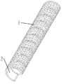
Links
Images


Classifications
-
- H—ELECTRICITY
- H10—SEMICONDUCTOR DEVICES; ELECTRIC SOLID-STATE DEVICES NOT OTHERWISE PROVIDED FOR
- H10N—ELECTRIC SOLID-STATE DEVICES NOT OTHERWISE PROVIDED FOR
- H10N10/00—Thermoelectric devices comprising a junction of dissimilar materials, i.e. devices exhibiting Seebeck or Peltier effects
- H10N10/01—Manufacture or treatment
-
- H01L35/34—
-
- H01L35/02—
-
- H01L35/22—
-
- H01L35/32—
-
- H—ELECTRICITY
- H10—SEMICONDUCTOR DEVICES; ELECTRIC SOLID-STATE DEVICES NOT OTHERWISE PROVIDED FOR
- H10N—ELECTRIC SOLID-STATE DEVICES NOT OTHERWISE PROVIDED FOR
- H10N10/00—Thermoelectric devices comprising a junction of dissimilar materials, i.e. devices exhibiting Seebeck or Peltier effects
- H10N10/10—Thermoelectric devices comprising a junction of dissimilar materials, i.e. devices exhibiting Seebeck or Peltier effects operating with only the Peltier or Seebeck effects
- H10N10/17—Thermoelectric devices comprising a junction of dissimilar materials, i.e. devices exhibiting Seebeck or Peltier effects operating with only the Peltier or Seebeck effects characterised by the structure or configuration of the cell or thermocouple forming the device
-
- H—ELECTRICITY
- H10—SEMICONDUCTOR DEVICES; ELECTRIC SOLID-STATE DEVICES NOT OTHERWISE PROVIDED FOR
- H10N—ELECTRIC SOLID-STATE DEVICES NOT OTHERWISE PROVIDED FOR
- H10N10/00—Thermoelectric devices comprising a junction of dissimilar materials, i.e. devices exhibiting Seebeck or Peltier effects
- H10N10/80—Constructional details
- H10N10/85—Thermoelectric active materials
- H10N10/851—Thermoelectric active materials comprising inorganic compositions
- H10N10/855—Thermoelectric active materials comprising inorganic compositions comprising compounds containing boron, carbon, oxygen or nitrogen
Landscapes
- Chemical & Material Sciences (AREA)
- Inorganic Chemistry (AREA)
- Engineering & Computer Science (AREA)
- Manufacturing & Machinery (AREA)
- Cooling Or The Like Of Semiconductors Or Solid State Devices (AREA)
- Photovoltaic Devices (AREA)
- Weting (AREA)
Abstract
본 개시는, x-선 광전자 분광법(x-ray photoelectron spectroscopy; XPS)에 의해 측정되는 약 1% 미만의 금속 함량을 가진 노출된 표면들을 갖는 가요성 반도체 기판을 포함하며, 적어도 약 0.25인 성능 지수(ZT)를 갖는 열전 엘러먼트로서, 가요성 반도체 기판은 25℃에서 약 1x10⁶ 제곱 인치 당 파운드(psi) 이하의 영률을 갖는, 열전 엘러먼트를 제공한다.This disclosure includes a flexible semiconductor substrate having exposed surfaces with a metal content of less than about 1% as measured by x-ray photoelectron spectroscopy (XPS), having a performance index of at least about 0.25 a thermal Element having a (ZT), the flexible semiconductor substrate provides, thermally Element having a Young's modulus of less than about 1x10 6 pounds per square inch (psi) at 25 ℃.

Description
상호-참조 Cross-reference
본 출원은, 2014년 03월 25일자로 출원된 미국 가특허 출원 번호 제61/970,322호, 및 2014년 06월 17일자로 출원된 미국 가특허 출원 번호 제62/013,468호에 대한 이익을 주장하며, 이들의 각각이 전체적으로 본원에 참조로서 포함된다.This application claims the benefit of US Provisional Patent Application No. 61 / 970,322, filed March 25, 2014, and US Provisional Patent Application No. 62 / 013,468, filed June 17, 2014 , Each of which is incorporated herein by reference in its entirety.
그들의 주요한 연료원으로서 석유를 필요로 하는 열 엔진들에 의해 전 세계적으로 매년 15 테라와트를 넘는 열이 환경으로 손실된다. 이는, 이러한 엔진들이 석유 화학적 에너지의 30 내지 40%만을 유용한 작업으로 변환하기 때문이다. 폐열(waste heat)의 생성은 열역학의 제 2 법칙의 회피할 수 없는 결과이다. Over 15 terawatts of heat are lost to the environment worldwide each year by heat engines that require oil as their primary source of fuel. This is because these engines convert only 30 to 40% of the petrochemical energy into useful work. The generation of waste heat is an inescapable consequence of the second law of thermodynamics.
용어 "열전 효과"는 제벡 효과(Seebeck effect), 펠티에 효과(Peltier effect) 및 톰슨 효과(Thomson effect)를 포괄한다. 열전 효과들에 기반하는 고체-상태 냉각 및 전력 생성은 전형적으로 전력 생성 및 열 펌핑을 위해 제벡 효과 또는 펠티에 효과를 이용한다. 그러나, 이러한 통상적인 열전 디바이스들의 유용성은 전형적으로 (냉각 애플리케이션들에 대한) 그들의 낮은 성능 계수(coefficient-of-performance; COP) 또는 (전력 생성 애플리케이션에 대한) 낮은 효율에 의해 제한된다. The term " thermoelectric effect " encompasses the Seebeck effect, the Peltier effect, and the Thomson effect. Solid-state cooling and power generation based on thermoelectric effects typically utilize a Seebeck effect or a Peltier effect for power generation and heat pumping. However, the utility of these conventional thermoelectric devices is typically limited by their low coefficient of performance (COP) or low efficiency (for power generation applications) (for cooling applications).
열전 디바이스 성능은, 소위 열전 성능 지수(figure-of-merit), 즉, Z = S2σ/k에 의해 획득되며, 여기에서 'S'는 제벡 계수이고, 'σ'는 전기 전도율이며, 'k'는 열 전도율이다. Z는 전형적으로 열전 디바이스들의 효율성 및 COP의 표시자로서 이용되며, 즉, COP가 Z와 함께 스케일링된다. 무차원(dimensionless) 성능 지수 ZT는 열전 디바이스 성능을 수량화하기 위하여 이용될 수 있으며, 여기에서 'T'는 디바이스의 뜨거운 측 및 차가운 측의 평균 온도일 수 있다. Thermoelectric device performance is obtained by a so-called figure-of-merit, i.e. Z = S 2 σ / k, where S is the Seebeck coefficient, σ is the electrical conductivity, k 'is the thermal conductivity. Z is typically used as an indicator of the efficiency and COP of the thermoelectric devices, i.e., the COP is scaled with Z. The dimensionless performance index ZT can be used to quantify thermoelectric device performance, where 'T' can be the average temperature on the hot and cold sides of the device.
통상적인 반도체 열전 냉각기들의 애플리케이션들은, 그들이 제공하는 다른 냉각 기술들을 뛰어 넘는 다수의 이점들에도 불구하고, 낮은 성능 지수의 결과로서 상당히 제한된다. 냉각 시에, 작은 성능 지수를 갖는 통상적인 열전 재료들로 만들어진 열전 디바이스들의 낮은 효율은 효율적인 열전 냉각을 제공함에 있어서 그들의 애플리케이션들을 제한한다.The applications of conventional semiconductor thermoelectric coolers are severely limited as a result of the low figure of merit, despite the many advantages over other cooling techniques they provide. During cooling, the low efficiency of thermoelectric devices made of conventional thermoelectric materials with a small figure of merit limits their applications in providing efficient thermoelectric cooling.
본 개시는 열전 엘러먼트들, 디바이스들 및 시스템들, 및 이러한 엘러먼트들, 디바이스들 및 시스템들을 형성하기 위한 방법들을 제공한다. The present disclosure provides thermoelectric elements, devices and systems, and methods for forming such elements, devices, and systems.
현재 이용가능한 열전 디바이스들이 존재하지만, 이러한 열전 디바이스들과 연관된 다양한 제한들이 본원에서 인식된다. 예를 들어, 현재 이용가능한 일부 열전 디바이스들은 가요성이 아닐 수 있고 다양한 형상들의 물체들에 맞춰지는 것이 불가능할 수 있으며, 이는 열 전달을 위한 표면적을 최대화하는 것을 어렵게 만든다. 다른 예로서, 현재 이용가능한 일부 열전 디바이스들이 상당히 두꺼우며, 더 콤팩트한 열전 디바이스들을 필요로 하는 전자 디바이스들 내에서 사용하기에 적절하지 않다. While there are currently available thermoelectric devices, various limitations associated with such thermoelectric devices are recognized herein. For example, some currently available thermoelectric devices may not be flexible and may not be able to fit to objects of various shapes, which makes it difficult to maximize the surface area for heat transfer. As another example, some currently available thermoelectric devices are fairly thick and not suitable for use in electronic devices that require more compact thermoelectric devices.
본 개시는 열전 엘러먼트들, 디바이스들 및 시스템들, 및 이러한 열전 엘러먼트들, 디바이스들 및 시스템들을 형성하기 위한 방법들을 제공한다. 본 개시의 열전 엘러먼트들 및 디바이스들은 가요성일 수 있고 다양한 형상들, 크기들 및 구성들의 물체에 맞춰지는 것이 가능할 수 있으며, 이는 이러한 엘러먼트들 및 디바이스들을 소비자 및 산업 환경들과 같은 다양한 환경들에서의 사용에 적합하게 만든다. 본 개시의 열전 엘러먼트들 및 디바이스들은 폐열을 수집하도록 표면들에 맞추어질 수 있으며 폐열의 적어도 일 부분을 사용가능한 에너지로 변환할 수 있다. 일부 경우들에 있어서, 폐열은 화학적, 전기적, 및/또는 기계적 열 변환 프로세스 동안 생성될 수 있다. The present disclosure provides thermoelectric elements, devices and systems, and methods for forming such thermoelectric elements, devices and systems. The thermoelectric elements and devices of the present disclosure may be flexible and may be able to be adapted to an object of various shapes, sizes and configurations, which may enable these elements and devices to be used in various environments such as consumer and industrial environments Making it suitable for use in. The thermoelectric elements and devices of the present disclosure may be adapted to surfaces to collect waste heat and may convert at least a portion of the waste heat to usable energy. In some cases, the waste heat may be generated during a chemical, electrical, and / or mechanical thermal conversion process.
본 개시의 일 측면에 있어서, 적어도 약 0.25인 성능 지수(ZT)를 갖는 열전 엘러먼트를 형성하기 위한 방법은, (a) 반도체 기판, 반도체 기판의 제 1 표면과 전기적으로 연통하는 작업 전극, 반도체 기판의 제 2 표면과 접촉하는 에칭 용액(예를 들어, 전해액), 및 에칭 용액 내의 상대 전극(counter electrode)을 포함하는 반응 공간을 제공하는 단계로서, 반도체 기판의 제 1 및 제 2 표면들은 실질적으로 금속성 코팅이 없는, 단계; 및 (b) 전극 및 상대 전극을 사용하여 (i) 적어도 약 0.1 mA/cm2의 전류 밀도로 전기적 전류를 반도체 기판으로 보내고, 및 (ii) 반도체 기판 내에 홀(hole)들의 패턴을 형성하기 위하여 반도체 기판의 제 2 표면을 에칭 용액으로 에칭함으로써 적어도 약 0.25인 ZT를 갖는 열전 엘러먼트를 형성하는 단계로서, 에칭은 반도체 기판 및 에칭 용액에 걸쳐 적어도 약 1 볼트(V)의 전기적 전위에서 수행되며, 에칭은 25℃에서 적어도 약 1 나노미터(nm)인 에칭 레이트(etch rate)를 갖는, 단계를 포함한다. 일부 실시예들에 있어서, 전기적 전위는 작업 전극, 에칭 용액 및 상대 전극에 걸쳐 적어도 약 1 볼트(V)이다. In one aspect of the present disclosure, a method for forming a thermoelectrically element having a figure of merit (ZT) of at least about 0.25 comprises the steps of: (a) providing a semiconductor substrate, a working electrode in electrical communication with the first surface of the semiconductor substrate, Providing a reaction space comprising an etchant solution (e.g., an electrolyte) in contact with a second surface of the substrate, and a counter electrode in the etch solution, wherein the first and second surfaces of the semiconductor substrate are substantially With no metallic coating; And (b) applying an electrical current to the semiconductor substrate at a current density of at least about 0.1 mA / cm < 2 > to form a pattern of holes in the semiconductor substrate, Forming a thermoelectric element having a ZT of at least about 0.25 by etching a second surface of the semiconductor substrate with an etching solution, wherein the etching is performed at an electrical potential of at least about 1 volt (V) across the semiconductor substrate and the etching solution , And the etching has an etch rate of at least about 1 nanometer (nm) at 25 占 폚. In some embodiments, the electrical potential is at least about 1 volt (V) across the working electrode, etching solution, and counter electrode.
일부 실시예들에 있어서, 전기적 전위는 교류(alternating current; AC) 전압이다. 일부 실시예들에 있어서, 전기적 전위는 직류(direct current; DC) 전압이다. In some embodiments, the electrical potential is an alternating current (AC) voltage. In some embodiments, the electrical potential is a direct current (DC) voltage.
일부 실시예들에 있어서, 작업 전극은 제 1 표면과 접촉한다. 일부 실시예들에 있어서, 작업 전극은 제 1 표면과 오믹(ohmic) 접촉한다. 일부 실시예들에 있어서, 반도체 기판은 작업 전극의 부분이다. In some embodiments, the working electrode contacts the first surface. In some embodiments, the working electrode is in ohmic contact with the first surface. In some embodiments, the semiconductor substrate is part of a working electrode.
일부 실시예들에 있어서, 에칭 레이트는 적어도 초당 약 10 nm이다. 일부 실시예들에 있어서, 에칭 레이트는 적어도 초당 약 100 nm이다. 일부 실시예들에 있어서, 에칭 레이트는 적어도 초당 약 1000 nm이다. In some embodiments, the etch rate is at least about 10 nm per second. In some embodiments, the etch rate is at least about 100 nm per second. In some embodiments, the etch rate is at least about 1000 nm per second.
일부 실시예들에 있어서, 전류 밀도는 적어도 약 1 mA/cm2이다. 일부 실시예들에 있어서, 전류 밀도는 적어도 약 10 mA/cm2이다. 일부 실시예들에 있어서, 전류 밀도는 약 10 mA/cm2 내지 50 mA/cm2, 10 mA/cm2 내지 30 mA/cm2, 또는 10 mA/cm2 내지 20 mA/cm2이다. 일부 실시예들에 있어서, 전류 밀도는 약 100 mA/cm2 또는 50 mA/cm2 이하이다. 일부 실시예들에 있어서, 반도체 기판은 상기 전류 밀도의 교류 하에서 에칭된다. In some embodiments, the current density is at least about 1 mA / cm 2 . In some embodiments, the current density is at least about 10 mA / cm 2 . In some embodiments, the current density is about 10 mA / cm 2 to 50 mA / cm 2 , 10 mA / cm 2 to 30 mA / cm 2 , or 10 mA / cm 2 to 20 mA / cm 2 . In some embodiments, the current density is about 100 mA / cm 2 or 50 mA / cm 2 or less. In some embodiments, the semiconductor substrate is etched under the alternating current density.
일부 실시예들에 있어서, 작업 전극은 에칭 동안 애노드(anode)이다. 일부 실시예들에 있어서, 방법은, (b) 단계 이후에 반도체 기판을 어닐링(anneal)하는 단계를 더 포함한다. 일부 실시예들에 있어서, 방법은, (b) 단계 이전에, 에칭 용액을 25℃보다 더 높은 온도까지 가열하는 단계를 더 포함한다. 일부 실시예들에 있어서, 반도체 기판은 금속 촉매 없이 (또는 금속 촉매의 도움 없이) 에칭된다. In some embodiments, the working electrode is an anode during etching. In some embodiments, the method further comprises annealing the semiconductor substrate after step (b). In some embodiments, the method further comprises heating the etch solution to a temperature greater than 25 占 폚, prior to step (b). In some embodiments, the semiconductor substrate is etched without a metal catalyst (or without the aid of a metal catalyst).
일부 실시예들에 있어서, 홀들의 패턴은 홀들의 무질서한 패턴을 포함한다. 일부 실시예들에 있어서, 작업 전극은 에칭 용액과 접촉하지 않는다. In some embodiments, the pattern of holes includes a disordered pattern of holes. In some embodiments, the working electrode is not in contact with the etching solution.
일부 실시예들에 있어서, 에칭 용액은 산을 포함한다. 일부 실시예들에 있어서, 산은 HF, HCl, HBr 및 HI로 구성된 그룹으로부터 선택된다. 일부 실시예들에 있어서, 에칭 용액은 알콜 첨가제를 포함한다. 일부 실시예들에 있어서, 에칭은 반도체 기판을 조명하지 않으면서 수행된다. In some embodiments, the etching solution comprises an acid. In some embodiments, the acid is selected from the group consisting of HF, HCl, HBr, and HI. In some embodiments, the etching solution comprises an alcohol additive. In some embodiments, the etching is performed without illuminating the semiconductor substrate.
일부 실시예들에 있어서, ZT는 25℃에서 적어도 0.5, 0.6, 0.7, 0.8, 0.9, 또는 1이다. 일부 실시예들에 있어서, 반도체 기판은 실리콘을 포함한다. In some embodiments, ZT is at least 0.5, 0.6, 0.7, 0.8, 0.9, or 1 at 25 占 폚. In some embodiments, the semiconductor substrate comprises silicon.
다른 측면에 있어서, 적어도 약 0.25인 성능 지수(ZT)를 갖는 열전 엘러먼트를 형성하기 위한 방법은, (a) 에칭 용액(예를 들어, 전해액)을 포함하는 반응 공간 내에 반도체 기판을 제공하는 단계; (b) 적어도 약 0.1 mA/cm2의 전류 밀도로 반도체 기판으로의 전기적 전류의 흐름을 유도하는 단계; 및 (c) 반도체 기판 내에 홀들의 무질서한 패턴을 형성하기 위하여 적어도 약 0.1 mA/cm2의 전류 밀도 하에서 에칭 용액을 사용하여 반도체 기판을 에칭함으로써, 적어도 약 0.25인 ZT를 갖는 열전 엘러먼트를 형성하는 단계로서, 에칭은 (i) 금속 촉매 없이 그리고 (ii) 반도체 기판과 에칭 용액에 걸친 적어도 약 1 볼트(V)의 전기적 전위에서 수행되며, 에칭은 25℃에서 적어도 초당 약 1 나노미터(nm)의 에칭 레이트를 갖는, 단계를 포함한다. In another aspect, a method for forming a thermoelectric element having a figure of merit (ZT) of at least about 0.25 comprises the steps of: (a) providing a semiconductor substrate in a reaction space comprising an etching solution ; (b) inducing a flow of electrical current into the semiconductor substrate at a current density of at least about 0.1 mA / cm 2 ; And (c) etching the semiconductor substrate using an etching solution under a current density of at least about 0.1 mA / cm < 2 > to form a disordered pattern of holes in the semiconductor substrate to form a thermoelectric element having a ZT of at least about 0.25 Wherein the etching is performed at a temperature of at least about 1 nanometer (nm) per second at 25 DEG C, and (ii) at least about 1 volts (V) of electrical potential across the semiconductor substrate and the etching solution, Of the etch rate.
일부 실시예들에 있어서, 전기적 전위는 교류(AC) 전압이다. 일부 실시예들에 있어서, 전기적 전위는 직류(DC) 전압이다. In some embodiments, the electrical potential is an alternating current (AC) voltage. In some embodiments, the electrical potential is a direct current (DC) voltage.
일부 실시예들에 있어서, 에칭 레이트는 적어도 초당 약 10 nm이다. 일부 실시예들에 있어서, 에칭 레이트는 적어도 초당 약 100 nm이다. 일부 실시예들에 있어서, 에칭 레이트는 적어도 초당 약 1000 nm이다. In some embodiments, the etch rate is at least about 10 nm per second. In some embodiments, the etch rate is at least about 100 nm per second. In some embodiments, the etch rate is at least about 1000 nm per second.
일부 실시예들에 있어서, 전류 밀도는 적어도 약 1 mA/cm2이다. 일부 실시예들에 있어서, 전류 밀도는 적어도 약 10 mA/cm2이다. 일부 실시예들에 있어서, 전류 밀도는 약 10 mA/cm2 내지 50 mA/cm2, 10 mA/cm2 내지 30 mA/cm2, 또는 10 mA/cm2 내지 20 mA/cm2이다. 일부 실시예들에 있어서, 전류 밀도는 약 100 mA/cm2 또는 50 mA/cm2 이하이다. 일부 실시예들에 있어서, 반도체 기판은 상기 전류 밀도의 교류 하에서 에칭된다. In some embodiments, the current density is at least about 1 mA / cm 2 . In some embodiments, the current density is at least about 10 mA / cm 2 . In some embodiments, the current density is about 10 mA / cm 2 to 50 mA / cm 2 , 10 mA / cm 2 to 30 mA / cm 2 , or 10 mA / cm 2 to 20 mA / cm 2 . In some embodiments, the current density is about 100 mA / cm 2 or 50 mA / cm 2 or less. In some embodiments, the semiconductor substrate is etched under the alternating current density.
일부 실시예들에 있어서, 에칭 용액은 산을 포함한다. 일부 실시예들에 있어서, 산은 HF, HCl, HBr 및 HI로 구성된 그룹으로부터 선택된다. 일부 실시예들에 있어서, 에칭 용액은 알콜 첨가제를 포함한다. 일부 실시예들에 있어서, 에칭은 반도체 기판을 조명하지 않으면서 수행된다. In some embodiments, the etching solution comprises an acid. In some embodiments, the acid is selected from the group consisting of HF, HCl, HBr, and HI. In some embodiments, the etching solution comprises an alcohol additive. In some embodiments, the etching is performed without illuminating the semiconductor substrate.
일부 실시예들에 있어서, 방법은, (c) 단계 이후에 반도체 기판을 어닐링하는 단계를 더 포함한다. 일부 실시예들에 있어서, 방법은, (c) 단계 이전에, 에칭 용액을 25℃보다 더 높은 온도까지 가열하는 단계를 더 포함한다. 일부 실시예들에 있어서, 반도체 기판은 실리콘을 포함한다. In some embodiments, the method further comprises annealing the semiconductor substrate after step (c). In some embodiments, the method further comprises heating the etch solution to a temperature greater than 25 占 폚, prior to step (c). In some embodiments, the semiconductor substrate comprises silicon.
본 개시의 또 다른 측면은, 하나 이상의 컴퓨터 프로세서들에 의한 실행 시에 이상의 또는 본원의 어떤 다른 곳의 방법들 중 임의의 방법을 구현하는 기계 실행가능 코드를 포함하는 컴퓨터 판독가능 매체를 제공한다. Another aspect of the present disclosure provides a computer readable medium comprising machine executable code that, when executed by one or more computer processors, embodies any of the above or any of the methods herein.
본 개시의 또 다른 측면은 하나 이상의 컴퓨터 프로세서 및 이에 결합된 메모리를 포함하는 컴퓨터 제어 시스템을 제공한다. 메모리는, 하나 이상의 컴퓨터 프로세서들에 의한 실행 시에 이상의 또는 본원의 어떤 다른 곳의 방법들 중 임의의 방법을 구현하는 기계 실행가능 코드를 포함한다. Another aspect of the disclosure provides a computer control system including one or more computer processors and a memory coupled to the one or more computer processors. The memory includes machine executable code that, when executed by one or more computer processors, implements any of the above or any of the methods described elsewhere herein.
본 개시의 또 다른 측면에 있어서, 열전 디바이스는 반도체 기판을 포함하는 적어도 하나의 가요성 열전 엘러먼트를 포함하며, 여기에서 반도체 기판의 표면들은 x-선 광전자 분광법(x-ray photoelectron spectroscopy; XPS)에 의해 측정되는 약 1% 미만의 금속 함량을 가지고, 여기에서 가요성 열전 엘러먼트는 25℃에서 적어도 약 0.25인 성능 지수(ZT)를 가지며, 여기에서 가요성 열전 엘러먼트는 25℃에서 열전 엘러먼트의 정적 편향(static deflection)에 의해 측정되는 약 1x10⁶ 제곱 인치 당 파운드(pounds per square inch; psi) 이하의 영률을 갖는다. In another aspect of the present disclosure, a thermoelectric device comprises at least one flexible thermoelement comprising a semiconductor substrate, wherein the surfaces of the semiconductor substrate are selected from the group consisting of x-ray photoelectron spectroscopy (XPS) Wherein the flexible thermoelectric element has a figure of merit (ZT) of at least about 0.25 at 25 DEG C, wherein the flexible thermoelectric element has a metal content of less than about 1% It has a Young's modulus of less than; (psi pounds per square inch) static deflection of about 1x10 6 pounds per jegop inchi as measured by the (static deflection) of the garment.
일부 실시예들에 있어서, 반도체 기판은 투과 전자 현미경검사(transmission electron microscopy; TEM)에 의해 측정되는 약 0.1 나노미터(nm) 내지 50 nm 사이의 표면 거칠기를 갖는다. 일부 실시예들에 있어서, 표면 거칠기는 TEM에 의해 측정될 때 약 1 nm 내지 20 nm 사이이다. 일부 실시예들에 있어서, 표면 거칠기는 TEM에 의해 측정될 때 약 1 nm 내지 10 nm 사이이다. In some embodiments, the semiconductor substrate has a surface roughness between about 0.1 nanometers (nm) and 50 nm measured by transmission electron microscopy (TEM). In some embodiments, the surface roughness is between about 1 nm and 20 nm as measured by TEM. In some embodiments, the surface roughness is between about 1 nm and 10 nm as measured by TEM.
일부 실시예들에 있어서, 금속 함량은 XPS에 의해 측정될 때 약 0.001% 이하이다. 일부 실시예들에 있어서, 영률은 25℃에서 약 800,000 psi 이하이다. 일부 실시예들에 있어서, 성능 지수는 적어도 약 0.5, 0.6, 0.7, 0.8, 0.9, 또는 1이다. In some embodiments, the metal content is less than about 0.001% as measured by XPS. In some embodiments, the Young's modulus is less than about 800,000 psi at 25 占 폚. In some embodiments, the figure of merit is at least about 0.5, 0.6, 0.7, 0.8, 0.9, or 1.
일부 실시예들에 있어서, 반도체 기판은 화학적으로 도핑된 n-형 또는 p-형이다. 일부 실시예들에 있어서, 반도체 기판은 실리콘을 포함한다. In some embodiments, the semiconductor substrate is a chemically doped n-type or p-type. In some embodiments, the semiconductor substrate comprises silicon.
일부 실시예들에 있어서, 열전 엘러먼트는 홀들의 패턴을 포함한다. 일부 실시예들에 있어서, 홀들의 패턴은 다분산성(polydisperse)이다. 일부 실시예들에 있어서, 홀들의 패턴은 홀들의 무질서한 패턴을 포함한다. 일부 실시예들에 있어서, 홀들의 무질서한 패턴은 다분산성이다. In some embodiments, the thermoelectric element comprises a pattern of holes. In some embodiments, the pattern of holes is polydisperse. In some embodiments, the pattern of holes includes a disordered pattern of holes. In some embodiments, the disordered pattern of holes is polydisperse.
일부 실시예들에 있어서, 열전 엘러먼트는 와이어(wire)들의 패턴을 포함한다. 일부 실시예들에 있어서, 와이어들의 패턴은 다분산성이다. 일부 실시예들에 있어서, 와이어들의 패턴은 와이어들의 무질서한 패턴을 포함한다. 일부 실시예들에 있어서, 와이어들의 무질서한 패턴은 다분산성이다. In some embodiments, the thermoelectric element comprises a pattern of wires. In some embodiments, the pattern of wires is polydisperse. In some embodiments, the pattern of wires includes a disordered pattern of wires. In some embodiments, the disordered pattern of wires is polydisperse.
본 개시의 또 다른 측면은, 반도체 기판을 포함한 적어도 하나의 가요성 열전 엘러먼트를 포함하는 전자 디바이스를 제공하며, 여기에서 반도체 기판의 표면들은 x-선 광전자 분광법(XPS)에 의해 측정되는 약 1% 미만의 금속 함량을 가지고, 여기에서 가요성 열전 엘러먼트는 25℃에서 적어도 약 0.25인 성능 지수(ZT)를 가지며, 여기에서 가요성 열전 엘러먼트는 3-점 테스팅(three-point testing)에 의해 측정되는 20% 미만인 소성 변형에서 측정 평면에 대하여 적어도 약 10°의 각도로 굽혀진다. Yet another aspect of the present disclosure provides an electronic device comprising at least one flexible thermoelectric element including a semiconductor substrate wherein surfaces of the semiconductor substrate are exposed to a temperature of about 1 < RTI ID = 0.0 > %, Wherein the flexible thermoelectric element has a figure of merit (ZT) of at least about 0.25 at 25 DEG C, wherein the flexible thermoelectric element is in a three-point testing Lt; RTI ID = 0.0 > 10 < / RTI > relative to the measurement plane.
일부 실시예들에 있어서, 반도체 기판은 투과 전자 현미경검사(TEM)에 의해 측정되는 약 0.1 나노미터(nm) 내지 50 nm 사이의 표면 거칠기를 갖는다. 일부 실시예들에 있어서, 표면 거칠기는 TEM에 의해 측정될 때 약 1 nm 내지 20 nm 사이이다. 일부 실시예들에 있어서, 표면 거칠기는 TEM에 의해 측정될 때 약 1 nm 내지 10 nm 사이이다. In some embodiments, the semiconductor substrate has a surface roughness between about 0.1 nanometers (nm) and 50 nm measured by transmission electron microscopy (TEM). In some embodiments, the surface roughness is between about 1 nm and 20 nm as measured by TEM. In some embodiments, the surface roughness is between about 1 nm and 10 nm as measured by TEM.
일부 실시예들에 있어서, 금속 함량은 XPS에 의해 측정될 때 약 0.001% 이하이다. 일부 실시예들에 있어서, 가요성 열전 엘러먼트는 측정 평면에 대하여 적어도 약 20°의 각도로 굽혀진다. 일부 실시예들에 있어서, 성능 지수는 적어도 약 0.5, 0.6, 0.7, 0.8, 0.9, 또는 1이다. In some embodiments, the metal content is less than about 0.001% as measured by XPS. In some embodiments, the flexible thermoelement is bent at an angle of at least about 20 with respect to the measurement plane. In some embodiments, the figure of merit is at least about 0.5, 0.6, 0.7, 0.8, 0.9, or 1.
일부 실시예들에 있어서, 전자 디바이스는, 시계, 건강 또는 피트니스 추적 디바이스이거나, 또는 폐열 회수 유닛이다. 전자 디바이스는, 예를 들어, 다른 전자 디바이스들 및 제어 모듈을 포함하는 더 큰 시스템의 부분일 수 있다. In some embodiments, the electronic device is a clock, health or fitness tracking device, or a waste heat recovery unit. The electronic device may be part of a larger system, including, for example, other electronic devices and a control module.
일부 실시예들에 있어서, 반도체 기판은 화학적으로 도핑된 n-형 또는 p-형이다. 일부 실시예들에 있어서, 반도체 기판은 실리콘을 포함한다. In some embodiments, the semiconductor substrate is a chemically doped n-type or p-type. In some embodiments, the semiconductor substrate comprises silicon.
일부 실시예들에 있어서, 전자 디바이스는 복수의 열전 엘러먼트들을 포함한다. 복수의 열전 엘러먼트들의 각각은 이상에서 또는 본원의 다른 어떤 곳에서 설명되는 것과 같을 수 있다. 일부 실시예들에 있어서, 복수의 열전 엘러먼트들은 반대로 화학적으로 도핑된 n-형 및 p-형이다. In some embodiments, the electronic device includes a plurality of thermoelectric elements. Each of the plurality of thermoelectric elements may be as described above or elsewhere herein. In some embodiments, the plurality of thermoelectrons are oppositely chemically doped n-type and p-type.
일부 실시예들에 있어서, 열전 엘러먼트는 홀들의 패턴을 포함한다. 일부 실시예들에 있어서, 홀들의 패턴은 다분산성이다. 일부 실시예들에 있어서, 홀들의 패턴은 홀들의 무질서한 패턴을 포함한다. 일부 실시예들에 있어서, 홀들의 무질서한 패턴은 다분산성이다. In some embodiments, the thermoelectric element comprises a pattern of holes. In some embodiments, the pattern of holes is polydisperse. In some embodiments, the pattern of holes includes a disordered pattern of holes. In some embodiments, the disordered pattern of holes is polydisperse.
일부 실시예들에 있어서, 열전 엘러먼트는 와이어들의 패턴을 포함한다. 일부 실시예들에 있어서, 와이어들의 패턴은 다분산성이다. 일부 실시예들에 있어서, 와이어들의 패턴은 와이어들의 무질서한 패턴을 포함한다. 일부 실시예들에 있어서, 와이어들의 무질서한 패턴은 다분산성이다. In some embodiments, the thermoelectric element comprises a pattern of wires. In some embodiments, the pattern of wires is polydisperse. In some embodiments, the pattern of wires includes a disordered pattern of wires. In some embodiments, the disordered pattern of wires is polydisperse.
본 개시의 또 다른 측면은, 유체를 보내기 위한 유체 흐름 채널; 및 유체 흐름 채널의 적어도 일 부분에 인접한 적어도 하나의 가요성 열전 엘러먼트를 포함하는 열전 디바이스를 포함하는 전력을 생성하기 위한 시스템을 제공하며, 여기에서 가요성 열전 엘러먼트는 25℃에서 약 1x10⁶ 제곱 인치 당 파운드(psi) 이하인 영률을 가지며, 여기에서 가요성 열전 엘러먼트는 유체 흐름 채널과 열적으로 연통하는 제 1 표면 및 열 싱크(heat sink)와 열적으로 연통하는 제 2 표면을 가지고, 여기에서 열전 디바이스는 유체 흐름 채널로부터 열 싱크로의 열전 디바이스를 통한 열의 흐름 시에 전력을 생성한다. Another aspect of the disclosure provides a fluid flow channel for delivering fluid; And a thermoelectric device including at least one flexible thermoelectric element adjacent at least a portion of the fluid flow channel, wherein the flexible thermoelectric element has a temperature of about 1 x 10 < RTI ID = 0.0 > Wherein the flexible thermoelectric element has a first surface in thermal communication with the fluid flow channel and a second surface in thermal communication with a heat sink, The thermoelectric device generates power during the flow of heat through the thermoelectric device from the fluid flow channel to the heat sink.
일부 실시예들에 있어서, 열전 디바이스는, 반대로 화학적으로 도핑된 n-형 및 p-형인 적어도 2개의 열전 엘러먼트들을 포함한다. 일부 실시예들에 있어서, 영률은 25℃에서 약 800,000 psi 이하이다. In some embodiments, the thermoelectric device comprises at least two thermoelectrons that are, conversely, chemically doped n-type and p-type. In some embodiments, the Young's modulus is less than about 800,000 psi at 25 占 폚.
일부 실시예들에 있어서, 열전 엘러먼트는 반도체 재료를 포함한다. 일부 실시예들에 있어서, 반도체 재료는 실리콘을 포함한다. In some embodiments, the thermoelectric element comprises a semiconductor material. In some embodiments, the semiconductor material comprises silicon.
일부 실시예들에 있어서, 가요성 열전 엘러먼트는 유체 흐름 채널의 형상에 실질적으로 맞춰진다. 일부 실시예들에 있어서, 유체 흐름 채널은 파이프이다. 일부 실시예들에 있어서, 유체 흐름 채널은 원통형이다. In some embodiments, the flexible thermoelement is substantially aligned with the shape of the fluid flow channel. In some embodiments, the fluid flow channel is a pipe. In some embodiments, the fluid flow channel is cylindrical.
본 개시의 추가적인 측면들 및 이점들이, 본 개시의 단지 예시적인 실시예들이 도시되고 설명되는 다음의 상세한 설명으로부터 당업자들에게 용이하게 명백해질 것이다. 이해될 바와 같이, 본 개시는, 본 개시로부터 일체 벗어나지 않으면서, 다른 그리고 상이한 실시예들이 가능하며, 그것의 몇몇 세부사항들은 다양하고 명백한 측면들에 있어서의 수정들이 가능하다. 따라서, 도면들 및 설명은 제한적이 아니라 사실상 예시적인 것으로 간주되어야 한다.Additional aspects and advantages of the present disclosure will become readily apparent to those skilled in the art from the following detailed description, in which only exemplary embodiments of the present disclosure are shown and described. As will be appreciated, this disclosure is capable of other and different embodiments, and its several details are capable of modifications in various obvious aspects, without departing from the present disclosure. Accordingly, the drawings and description are to be regarded as illustrative in nature, and not as restrictive.
참조에 의한 통합 Integration by reference
본 명세서에서 언급되는 모든 공개문헌들, 특허들, 및 특허 출원들은, 각각의 개별적인 공개문헌, 특허, 또는 특허 출원이 명확하고 개별적으로 참조로서 포함되는 것으로 표시되는 것과 동일한 정도로 본원에 참조로서 포함된다.All publications, patents, and patent applications mentioned in this specification are herein incorporated by reference to the same extent as if each individual publication, patent, or patent application was specifically and individually indicated to be incorporated by reference .
본 발명의 신규한 특징들이 특히 첨부된 청구항들에 기술된다. 본 발명의 특징들 및 이점들의 더 양호한 이해는, 그 안에서 본 발명의 원리들이 사용되는 예시적인 실시예들을 기술하는 다음의 상세한 설명, 및 (본원에서 "그림" 및 "도"로도 지칭되는) 첨부된 도면들을 참조함으로써 획득될 수 있다.
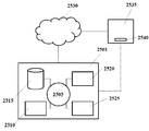
도 1은 복수의 엘러먼트들을 갖는 열전 디바이스를 도시한다.
도 2는 본 개시의 일 실시예에 따른 열전 엘러먼트의 개략적인 사시도이다.
도 3은 본 개시의 일 실시예에 따른 도 2의 열전 엘러먼트의 개략적인 평면도이다.
도 4는 본 개시의 일 실시예에 따른 도 2 및 도 3의 열전 엘러먼트의 개략적인 측면도이다.
도 5는 본 개시의 일 실시예에 따른 열전 엘러먼트의 개략적인 상단 사시도이다.
도 6은 본 개시의 일 실시예에 따른 도 5의 열전 엘러먼트의 개략적인 상단 사시도이다.
도 7은 본 개시의 일 실시예에 와이어들의 어레이를 갖는 엘러먼트들을 포함하는 열전 디바이스의 개략적인 사시도이다.
도 8은 본 개시의 일 실시예에 홀들의 어레이를 갖는 엘러먼트들을 포함하는 열전 디바이스의 개략적인 사시도이다.
도 9는 본 개시의 일 실시예에 따른, 벡터 V에 대하여 수직으로 배향된 홀들의 어레이를 갖는 엘러먼트들을 포함하는 열전 디바이스의 개략적인 사시도이다.
도 10은 복수의 열전 엘러먼트들을 포함하는 가요성 열전 디바이스를 제조하기 위한 방법을 개략적으로 예시한다.
도 11은 가요성 열전 재료를 갖는 가요성 열전 디바이스를 개략적으로 예시한다.
도 12는 열 싱크 및 열전 디바이스를 포함하는 열 회수 시스템을 개략적으로 예시한다.
도 13은 통합된 열전 디바이스 및 열 싱크들을 갖는 용접가능(weldable) 튜브를 개략적으로 예시한다.
도 14a는 물체 둘레에 감겨진 가요성 열 싱크를 개략적으로 예시하며; 도 14b는 도 14a의 측면 단면도이다.
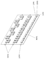
도 15는 통합된 열 싱크를 갖는 가요성 열전 테이프를 개략적으로 예시한다.
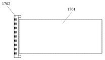
도 16은 상단 및 하단 상호연결부들과 전기적으로 연통하는 열전 엘러먼트들을 갖는 전자 디바이스를 개략적으로 예시한다.
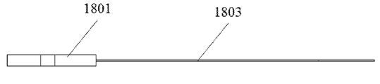
도 17a는 베이비 모니터(baby monitor)의 개략적인 측면 사시도이며; 도 17b는 도 17a의 베이비 모니터의 개략적인 각진 측면도이고; 도 17c는 도 17a의 베이비 모니터의 개략적인 측면도이며; 도 17d는 도 17a의 베이비 모니터의 개략적인 평면도이다.
도 18a는 페이스메이커(pacemaker)의 개략적인 측면 사시도이며; 도 18b는 도 18a의 페이스메이커의 개략적인 측면도이고; 도 18c는 도 18a의 페이스메이커의 개략적인 평면도이다.
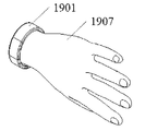
도 19a는 착용형(wearable) 전자 디바이스의 개략적인 사시도이며; 도 19b는 사용자의 손에 인접한 도 19a의 착용형 전자 디바이스를 개략적으로 예시한다.
도 20은 아이웨어(eyewear)의 개략적인 사시도이다.
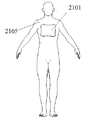
도 21a는 의료 디바이스의 개략적인 사시도이며; 도 21b는 사용자의 신체 상에 장착된 도 21a의 의료 디바이스를 개략적으로 예시한다.
도 22는 차량 배기 시스템의 부분으로서의 열 회수 시스템들을 개략적으로 예시한다.
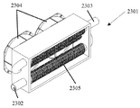
도 23a는 라디에이터 상에 설치된 열 회수 및 전력 생성 시스템의 개략적인 측면 사시도이며; 도 23b는 도 23a의 열 회수 및 전력 생성 시스템의 개략적인 측면도이다.
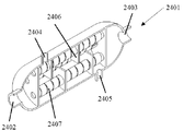
도 24a는 열 교환기 내에 설치된 열 회수 및 전력 생성 시스템의 개략적인 측면 사시도이며; 도 24b는 도 24a의 열 회수 및 전력 생성 시스템의 개략적인 측면도이다.
도 25는, 열전 엘러먼트들을 제조하는 것과 같은 본원에서 제공되는 다양한 방법들을 구현하도록 프로그래밍되거나 또는 달리 구성되는 컴퓨터 제어 시스템을 도시한다.
도 26a는 열전 엘러먼트의 주사 전자 현미경검사(scanning electron microscopy; SEM)의 현미경 사진을 도시하며, 도 26b는 열전 엘러먼트 내의 벌크(bulk) 및 다공성 실리콘을 보여주는 x-선 회절(XRD) 플롯(plot)을 도시한다.The novel features of the invention are set forth with particularity in the appended claims. BRIEF DESCRIPTION OF THE DRAWINGS A better understanding of the features and advantages of the present invention may be obtained through the following detailed description, which describes exemplary embodiments in which the principles of the invention are employed, and the accompanying drawings (also referred to herein as " By referring to the drawings.
Figure 1 shows a thermoelectric device having a plurality of elements.
2 is a schematic perspective view of a thermoelectric element according to one embodiment of the present disclosure;
Figure 3 is a schematic plan view of the thermoelectric element of Figure 2 in accordance with one embodiment of the present disclosure;
Figure 4 is a schematic side view of the thermoelectric element of Figures 2 and 3 in accordance with one embodiment of the present disclosure.
5 is a schematic top, perspective view of a thermoelectric element in accordance with one embodiment of the present disclosure;
Figure 6 is a schematic top, perspective view of the thermoelectric element of Figure 5 in accordance with one embodiment of the present disclosure;
7 is a schematic perspective view of a thermoelectric device including elements having an array of wires in an embodiment of the present disclosure;
8 is a schematic perspective view of a thermoelectric device including elements having an array of holes in one embodiment of the present disclosure;
9 is a schematic perspective view of a thermoelectric device including elements having an array of holes oriented perpendicular to a vector V, according to one embodiment of the present disclosure.
10 schematically illustrates a method for manufacturing a flexible thermoelectric device including a plurality of thermoelectrons.
Figure 11 schematically illustrates a flexible thermoelectric device having a flexible thermoelectric material.
Figure 12 schematically illustrates a heat recovery system including a heat sink and a thermoelectric device.
Figure 13 schematically illustrates a weldable tube having integrated thermoelectric devices and heat sinks.
Figure 14A schematically illustrates a flexible heat sink wound around an object; 14B is a side sectional view of Fig. 14A.
Figure 15 schematically illustrates a flexible thermoelectric tape having an integrated heat sink.
Figure 16 schematically illustrates an electronic device having thermoelectric elements in electrical communication with the top and bottom interconnections.
17A is a schematic side perspective view of a baby monitor; Figure 17b is a schematic angled side view of the baby monitor of Figure 17a; Figure 17c is a schematic side view of the baby monitor of Figure 17a; 17D is a schematic plan view of the baby monitor of FIG. 17A.
18A is a schematic side elevation view of a pacemaker; Figure 18b is a schematic side view of the pacemaker of Figure 18a; Figure 18c is a schematic plan view of the pacemaker of Figure 18a.
19A is a schematic perspective view of a wearable electronic device; Figure 19b schematically illustrates the wearable electronic device of Figure 19a adjacent to the user's hand.
Figure 20 is a schematic perspective view of an eyewear.
21A is a schematic perspective view of a medical device; Figure 21b schematically illustrates the medical device of Figure 21a mounted on the body of a user.
22 schematically illustrates heat recovery systems as part of a vehicle exhaust system.
23A is a schematic side elevation view of a heat recovery and power generation system installed on a radiator; Figure 23B is a schematic side view of the heat recovery and power generation system of Figure 23A.
24A is a schematic side elevation view of a heat recovery and power generation system installed in a heat exchanger; Figure 24B is a schematic side view of the heat recovery and power generation system of Figure 24A.
Figure 25 illustrates a computer control system that is programmed or otherwise configured to implement the various methods provided herein, such as to produce thermoelectric elements.
Figure 26a shows a micrograph of a scanning electron microscopy (SEM) of a thermoelement, Figure 26b shows an x-ray diffraction (XRD) plot (Fig. 26b) showing the bulk and porous silicon in the thermoelectric element plot.
본 발명의 다양한 실시예들이 본원에서 도시되고 설명되지만, 이러한 실시예들이 오로지 예로서 제공된다는 것이 당업자들에게 명백할 것이다. 다수의 변형들, 변화들, 및 대체들이 본 발명으로부터 벗어나지 않고 당업자들에게 일어날 수 있다. 본원에서 설명되는 본 발명의 실시예들에 대한 다양한 대안예들이 이용될 수 있다는 것이 이해되어야만 한다. While various embodiments of the invention have been illustrated and described herein, it will be apparent to those skilled in the art that these embodiments are provided by way of example only. Numerous variations, changes, and substitutions can occur to those skilled in the art without departing from the invention. It should be understood that various alternatives to the embodiments of the invention described herein may be utilized.
본원에서 사용되는 용어 "나노구조체(nanostructure)"는 일반적으로, 크기에 있어서 약 1 마이크로미터("마이크론") 미만인 제 1 축을 따른 제 1 치수(예를 들어, 폭)를 갖는 구조체를 지칭한다. 이러한 나노구조체들은, 제 1 축에 직각인 제 2 축을 따라서, 나노미터들 또는 더 작은 것으로부터 마이크론들, 밀리미터들 또는 더 큰 것까지의 제 2 치수를 가질 수 있다. 일부 경우들에 있어서, 치수(예를 들어, 폭)는 약 1000 나노미터("nm"), 또는 500 nm, 또는 100 nm, 또는 50 nm, 또는 더 작은 것보다 더 작다. 나노구조체들은 기판 재료 내에 형성된 홀들을 포함할 수 있다. 홀들은 홀들의 어레이를 갖는 메시(mesh)를 형성할 수 있다. 다른 경우들에 있어서, 나노구조체는 로드-형(rod-like) 구조체들, 예컨대 와이어들, 원통들 또는 박스-형 구조체를 포함할 수 있다. 로드-형 구조체들은, 원형, 타원형, 삼각형, 정사각형, 직사각형, 오각형, 육각형, 칠각형, 팔각형, 또는 구각형, 또는 다른 단면들을 가질 수 있다. The term "nanostructure " as used herein generally refers to a structure having a first dimension (e.g., width) along a first axis that is less than about one micrometer in size. These nanostructures can have a second dimension from nanometers or smaller to microns, millimeters or larger, along a second axis perpendicular to the first axis. In some cases, the dimensions (e.g., width) are smaller than about 1000 nanometers ("nm"), or 500 nm, or 100 nm, or 50 nm, or smaller. The nanostructures may include holes formed in the substrate material. The holes may form a mesh having an array of holes. In other instances, the nanostructure may include rod-like structures, such as wires, cylinders, or box-like structures. The rod-like structures may have a circular, elliptical, triangular, square, rectangular, pentagonal, hexagonal, hexagonal, octagonal, or rectangular, or other cross-section.
본원에서 사용되는 용어 "나노홀(nanohole)"은 일반적으로, 약 1000 나노미터("nm"), 또는 500 nm, 또는 100 nm, 또는 50 nm, 또는 더 작은 것 이하의 폭 또는 직경을 갖는, 충전된 또는 충전되지 않은 홀을 지칭한다. 금속, 반도체, 또는 절연 재료로 충전된 나노홀이 "나노포함체(nanoinclusion)"로 지칭될 수 있다. The term "nanohole " as used herein generally refers to a material having a width or diameter of less than about 1000 nanometers (" nm "), or 500 nm, or 100 nm, or 50 nm, Refers to charged or uncharged holes. Nano-holes filled with metals, semiconductors, or insulating materials can be referred to as "nanoinclusion ".
본원에서 사용되는 용어 "나노와이어(nanowire)"는 일반적으로, 약 1000 nm, 또는 500 nm, 또는 100 nm, 또는 50 nm, 또는 더 작은 것 이하의 폭 또는 직경을 갖는 와이어 또는 다른 세장형(elongate) 구조체를 지칭한다. The term "nanowire " as used herein generally refers to a wire or other elongate wire having a width or diameter of less than or equal to about 1000 nm, or 500 nm, or 100 nm, or 50 nm, ) Structure.
본원에서 사용되는 용어 "n-형"은 일반적으로 n-형 도펀트(dopant)로 화학적으로 도핑된("도핑된") 재료를 지칭한다. 예를 들어, 실리콘이 인 또는 비소를 사용하여 n-형 도핑될 수 있다. The term "n-type" as used herein generally refers to a material chemically doped ("doped") with an n-type dopant. For example, silicon may be n-type doped using phosphorous or arsenic.
본원에서 사용되는 용어 "p-형"은 일반적으로 p-형 도펀트로 화학적으로 도핑된 재료를 지칭한다. 예를 들어, 실리콘은 붕소 또는 알루미늄을 사용하여 p-형 도핑될 수 있다. The term "p-type" as used herein generally refers to a material that is chemically doped with a p-type dopant. For example, silicon may be p-type doped using boron or aluminum.
본원에서 사용되는 용어 "금속성"은 일반적으로 금속성 속성들을 나타내는 물질을 지칭한다. 금속성 재료는 하나 이상의 원소 금속들을 포함할 수 있다. As used herein, the term "metallic" refers to materials that generally exhibit metallic properties. The metallic material may comprise one or more elemental metals.
본원에서 사용되는 용어 "단분산성(monodisperse)"은 일반적으로, 서로 유사한 형상들, 크기들(예를 들어, 폭들, 단면들, 볼륨들) 또는 분포들(예를 들어, 최인접 이웃 간격, 중심-대-중심 간격)을 갖는 특징부들을 지칭한다. 일부 예들에 있어서, 단분산성 특징부들(예를 들어, 홀들, 와이어들)은 서로 최대한으로 약 20%, 15%, 10%, 5%, 4%, 3%, 2%, 1%, 0.5%, 또는 0.1%만큼 편차가 있는 형상들 또는 크기들을 갖는다. 일부 경우들에 있어서, 단분산성 특징부들은 실질적으로 단분산성이다. As used herein, the term "monodisperse" generally refers to shapes, sizes (e.g., widths, cross sections, volumes) or distributions (e.g., To-center spacing). In some instances, the monodisperse features (e. G., The holes, wires) are at most about 20%, 15%, 10%, 5%, 4%, 3%, 2%, 1% , Or 0.1%. ≪ / RTI > In some cases, the monodisperse features are substantially monodisperse.
본원에서 사용되는 용어 "에칭 재료"는 일반적으로 에칭 재료에 인접한 기판(예를 들어, 반도체 기판)의 에칭을 용이하게 하는 재료를 지칭한다. 일부 경우들에 있어서, 에칭 재료는, 산화제 및 화학적 에칭제(etchant)에 대한 에칭 재료의 노출 시에 기판의 에칭을 촉진한다. The term "etch material " as used herein generally refers to a material that facilitates etching of a substrate (e.g., a semiconductor substrate) adjacent to the etch material. In some cases, the etch material facilitates etching of the substrate upon exposure of the etchant to the oxidant and the chemical etchant.
본원에서 사용되는 용어 "에칭 층"은 일반적으로 에칭 재료를 포함하는 층을 지칭한다. 에칭 재료들의 예들은, 은, 백금, 크롬, 몰리브덴, 텅스텐, 오스뮴, 이리듐, 로듐, 루테늄, 팔라듐, 구리, 니켈 및 다른 금속들(예를 들어, 귀금속들), 또는 이들의 임의의 조합, 또는, 예를 들어, 구리, 니켈, 또는 이들의 조합과 같은, 화학적 산화제의 분해를 촉진할 수 있는 임의의 비-귀금속을 포함한다. The term "etch layer" as used herein generally refers to a layer comprising an etch material. Examples of etch materials are silver, platinum, chromium, molybdenum, tungsten, osmium, iridium, rhodium, ruthenium, palladium, copper, nickel and other metals (e.g., precious metals) , And any non-noble metal capable of promoting the decomposition of a chemical oxidant, such as, for example, copper, nickel, or combinations thereof.
본원에서 사용되는 용어 "에칭 차단 재료"는 일반적으로 에칭 차단 재료에 인접한 기판의 에칭을 차단하거나 또는 달리 방해하는 재료를 지칭한다. 에칭 차단 재료는, 에칭 재료와 연관된 기판 에칭 레이트에 관하여, 감소되거나 또는 일부 경우들에서 실질적으로 감소된 기판 에칭 레이트를 제공할 수 있다. 본원에서 사용되는 용어 "에칭 차단 층"은 일반적으로 에칭 차단 재료를 포함하는 층을 지칭한다. 에칭 차단 재료는 에칭 재료의 에칭 레이트보다 더 낮은 에칭 레이트를 가질 수 있다. The term "etch barrier material " as used herein generally refers to a material that blocks or otherwise interferes with the etching of a substrate adjacent to the etch barrier material. The etch barrier material may provide a substrate etch rate that is reduced or substantially reduced in some cases with respect to the substrate etch rate associated with the etch material. The term "etch barrier layer " as used herein generally refers to a layer comprising an etch barrier material. The etch barrier material may have an etch rate that is lower than the etch rate of the etch material.
본원에서 사용되는 용어 "반응 공간"은 일반적으로 열전 디바이스의 컴포넌트 또는 열전 디바이스의 형성에 적절한 임의의 환경을 지칭한다. 반응 공간은 기판에 인접한 재료 필름 또는 얇은 필름의 증착을 위해, 또는 재료 필름 또는 얇은 필름의 물리적 특성들의 측정을 위해 적절할 수 있다. 반응 공간은, 복수의 챔버들을 갖는 시스템 내의 챔버일 수 있는 챔버를 포함할 수 있다. 시스템은 복수의 유체적으로 분리된(또는 격리된) 챔버들을 포함할 수 있다. 시스템은, 각각의 반응 공간이 다른 반응 공간으로부터 유체적으로 분리된 복수의 반응 공간들을 포함할 수 있다. 반응 공간은 기판에 인접하여 형성된 얇은 필름 또는 기판에 대한 측정들을 수행하기에 적절할 수 있다. As used herein, the term "reaction space" refers generally to any component of a thermoelectric device or any environment suitable for the formation of a thermoelectric device. The reaction space may be suitable for deposition of a material film or thin film adjacent to the substrate, or for measurement of the physical properties of the material film or thin film. The reaction space may comprise a chamber, which may be a chamber in a system having a plurality of chambers. The system may include a plurality of fluidically separated (or isolated) chambers. The system may include a plurality of reaction spaces in which each reaction space is fluidly separated from the other reaction spaces. The reaction space may be suitable for performing measurements on a thin film or substrate formed adjacent to the substrate.
본원에서 사용되는 용어 "전류 밀도"는 일반적으로 기판의 단면과 같은 단면의 단위 면적 당의 전기(또는 전기적) 전류를 지칭한다. 일부 예들에 있어서, 전류 밀도는 반도체 기판의 표면의 단위 면적 당의 전기적 전류이다. The term "current density" as used herein generally refers to electrical (or electrical) current per unit area of a cross section, such as a cross section of a substrate. In some examples, the current density is an electrical current per unit area of the surface of the semiconductor substrate.
본원에서 사용되는 용어 "인접한" 또는 "~에 인접한"은 '~의 다음의', '접하는', '~과 접촉하는' 및 '~에 근접한'을 포함한다. 일부 경우들에 있어서, 인접한 컴포넌트들은 하나 이상의 개재(intervening) 층들에 의해 서로 분리된다. 하나 이상의 개재 층들은 약 10 마이크로미터("마이크론"), 1 마이크로, 500 나노미터("nm"), 100 nm, 50 nm, 10 nm, 1 nm, 0.5 nm 또는 그 미만보다 더 작은 두께를 가질 수 있다. 예를 들어, 제 2 층에 인접한 제 1 층은 제 2 층과 직접 접촉할 수 있다. 다른 예로서, 제 2 층에 인접한 제 1 층은 적어도 제 3 층에 의해 제 2 층으로부터 분리될 수 있다. As used herein, the terms "adjacent" or "adjacent to" include "next to," "contacting," "in contact with," and "proximity to." In some cases, adjacent components are separated from each other by one or more intervening layers. The one or more intervening layers may have a thickness less than about 10 micrometers ("micron"), 1 micron, 500 nanometers ("nm"), 100 nm, 50 nm, 10 nm, 1 nm, 0.5 nm, . For example, the first layer adjacent to the second layer may be in direct contact with the second layer. As another example, the first layer adjacent to the second layer may be separated from the second layer by at least a third layer.
열전 엘러먼트들, 디바이스들 및 시스템들 Thermoelectric elements, devices and systems
본 개시는, 가열 및/또는 냉각 애플리케이션들, 전력 생성, 소비자 애플리케이션들 및 산업 애플리케이션들과 같은 다양한 애플리케이션들에서의 사용을 위하여 이용될 수 있는 열전 엘러먼트들, 디바이스들 및 시스템들을 제공한다. 일부 예들에 있어서, 열전 재료들은 소비자 전자 디바이스들(예를 들어, 스마트 시계, 휴대용 전자 디바이스들, 및 건강/피트니스 추적 디바이스들)에서 사용된다. 다른 예로서, 본 개시의 열전 재료는 열 손실이 존재하는 위치에서와 같이 산업 환경에서 사용될 수 있다. 이러한 경우에 있어서, 열이 열전 디바이스에 의해 포획되고 전력을 생성하기 위하여 사용될 수 있다. The present disclosure provides thermoelectric elements, devices, and systems that can be used for various applications such as heating and / or cooling applications, power generation, consumer applications, and industrial applications. In some instances, thermoelectric materials are used in consumer electronic devices (e.g., smart clocks, portable electronic devices, and health / fitness tracking devices). As another example, the thermoelectric materials of the present disclosure can be used in industrial environments, such as at locations where heat loss is present. In this case, heat can be captured by the thermoelectric device and used to generate power.
본 개시의 열전 디바이스들은, 이러한 디바이스에 걸친 온도 구배(gradient)의 인가 시에 전력을 생성하기 위하여 사용될 수 있다. 이러한 전력은 소비자 전자 디바이스들과 같은 다양한 유형들의 디바이스들에 전기적 에너지를 제공하기 위하여 사용될 수 있다. The thermoelectric devices of the present disclosure can be used to generate power upon application of a temperature gradient across such a device. This power can be used to provide electrical energy to various types of devices, such as consumer electronic devices.
본 개시의 열전 디바이스들은 다양한 비-제한적인 이점들 및 이득들을 가질 수 있다. 일부 경우들에 있어서, 열전 디바이스는, 최적 열전 디바이스 성능을 위해 적절할 수 있는, 실질적으로 큰 종횡비들, 홀들 또는 와이어들의 균일성, 및 성능 지수 ZT를 가질 수 있다. 성능 지수에 대하여, Z는 열전 디바이스의 효율 및 성능 계수(coefficient-of-performance; COP)의 표시자일 수 있으며, T는 열전 디바이스의 뜨거운 측과 차가운 측의 평균 온도일 수 있다. 일부 실시예들에 있어서, 열전 디바이스 또는 열전 엘러먼트의 성능 지수(ZT)는, 25℃에서 적어도 약 0.01, 0.02, 0.03, 0.04, 0.05, 0.06, 0.07, 0.08, 0.09, 0.1, 0.15, 0.2, 0.25, 0.3, 0.35, 0.4, 0.45 0.5, 0.55, 0.6, 0.65, 0.7, 0.75, 0.8, 0.85, 0.9, 0.95, 1.0, 1.1, 1.2, 1.3, 1.4, 1.5, 1.6, 1.7, 1.8, 1.9, 2.0, 2.1, 2.2, 2.3, 2.4, 2.5, 2.6, 2.7, 2.8, 2.9, 또는 3.0이다. 일부 경우에 있어서, 성능 지수는 25℃에서 약 0.01 내지 3, 0.1 내지 2.5, 0.5 내지 2.0 또는 0.5 내지 1.5이다. The thermoelectric devices of the present disclosure may have a variety of non-limiting advantages and benefits. In some cases, a thermoelectric device may have a substantially large aspect ratio, uniformity of holes or wires, and a figure of merit ZT, which may be suitable for optimal thermoelectric device performance. For a figure of merit, Z may be an indicator of the efficiency and coefficient-of-performance (COP) of the thermoelectric device, and T may be the average temperature on the hot and cold sides of the thermoelectric device. In some embodiments, the figure of merit (ZT) of the thermoelectric device or thermoelectric element is at least about 0.01, 0.02, 0.03, 0.04, 0.05, 0.06, 0.07, 0.08, 0.09, 0.1, 0.15, 0.2, 0.8, 0.85, 0.9, 0.95, 1.0, 1.1, 1.2, 1.3, 1.4, 1.5, 1.6, 1.7, 1.8, 1.9, 2.0, 0.5, 0.5, 0.5, 0.6, 0.65, 0.7, 0.75, , 2.1, 2.2, 2.3, 2.4, 2.5, 2.6, 2.7, 2.8, 2.9, or 3.0. In some cases, the figure of merit is about 0.01 to 3, 0.1 to 2.5, 0.5 to 2.0 or 0.5 to 1.5 at 25 占 폚.
성능 지수(ZT)는 온도의 함수일 수 있다. 일부 경우들에 있어서, ZT는 온도와 함께 증가한다. 예를 들어, 25℃에서 0.5의 ZT를 갖는 열전체(thermoelectric)는 100℃에서 더 큰 ZT를 가질 수 있다. The figure of merit (ZT) can be a function of temperature. In some cases, ZT increases with temperature. For example, a thermoelectric with a ZT of 0.5 at 25 [deg.] C may have a larger ZT at 100 [deg.] C.
본 개시의 열전 디바이스들은 각기 나노구조체들(예를 들어, 홀들 또는 와이어들)을 포함하는 전극들을 가질 수 있다. 나노구조체들의 어레이는 복수의 홀들 또는 세장형 구조체들, 예컨대 와이어들(예를 들어, 나노와이어들)을 포함할 수 있다. 홀들 또는 와이어들은 정돈될 수 있으며 균일한 크기들 및 분포들을 가질 수 있다. 대안예로서, 홀들 또는 와이어들이 정돈되지 않을 수 있고 균일한 분포를 갖지 않을 수 있다. 일부 예들에 있어서, 홀들 또는 와이어들에 대하여 장거리 질서(long range order)가 존재하지 않는다. 일부 경우들에 있어서, 홀들 또는 와이어들이 랜덤한 방향들에서 서로 교차할 수 있다. 나노구조체들(예를 들어, 홀들 또는 와이어들)의 패턴화된 또는 무질서한 패턴들을 형성하기 위한 방법들이 본원의 다른 곳에 제공된다. The thermoelectric devices of the present disclosure may each have electrodes comprising nanostructures (e.g., holes or wires). The array of nanostructures may comprise a plurality of holes or elongate structures, e.g., wires (e.g., nanowires). The holes or wires can be trimmed and can have uniform sizes and distributions. As an alternative, the holes or wires may not be tidy and may not have a uniform distribution. In some instances, there is no long range order for holes or wires. In some cases, the holes or wires may cross each other in random directions. Methods for forming patterned or disordered patterns of nanostructures (e. G., Holes or wires) are provided elsewhere herein.
본 개시는 가요성이거나 또는 실질적으로 가요성인 열전 엘러먼트들을 제공한다. 가요성 재료는, 소성 변형을 경험하지 않고 형상에 맞춰질 수 있거나, 뒤틀릴 수 있거나, 또는 굽혀질 수 있는 재료일 수 있다. 이는, 열 소스 또는 열 싱크와의 접촉 면적이 중요한 환경들과 같은 다양한 환경들에서 열전 엘러먼트들이 사용되는 것을 가능하게 할 수 있다. 예를 들어, 가요성 열전 엘러먼트는, 예컨대 열 소스 또는 열 싱크 둘레에 열전 엘러먼트를 감음으로써 열 소스 또는 열 싱크와 효율적으로 접촉하게끔 될 수 있다. The present disclosure provides thermoelectric elements that are flexible or substantially flexible. The flexible material may be a material that can be shaped, twisted, or bent without experiencing plastic deformation. This may enable thermoelectric elements to be used in a variety of environments, such as environments where the contact area with a heat source or heat sink is critical. For example, a flexible thermoelectric element may be brought into effective contact with a heat source or heat sink, for example by winding a thermoelectric element around the heat source or heat sink.
열전 디바이스는 하나 이상의 열전 엘러먼트들을 포함할 수 있다. 열전 엘러먼트들은 가요성일 수 있다. 개별적인 열전 엘러먼트는 가요성일 수 있는 적어도 하나의 반도체 기판을 포함할 수 있다. 일부 경우들에 있어서, 열전 엘러먼트의 개별적인 반도체 기판들은, 이들이 서로 인접하여 배치될 때 가요성 열전 엘러먼트를 제공하도록 강성(rigid)이지만 상당히 얇다(예를 들어, 500 nm 내지 1 mm 또는 1 마이크로미터 내지 0.5 mm). 유사하게, 열전 디바이스의 개별적인 열전 엘러먼트는, 이들이 서로 인접하여 배치될 때 가요성 열전 디바이스를 제공하도록 강성이지만 상당히 얇을 수 있다. A thermoelectric device can include one or more thermoelectric elements. Thermoelectric elements can be flexible. The individual thermoelectric elements may include at least one semiconductor substrate that may be flexible. In some cases, the individual semiconductor substrates of the thermoelectrons are rigid but considerably thin (e.g., between 500 nm and 1 mm or 1 micron) to provide a flexible thermoelement when they are disposed adjacent to each other Meter to 0.5 mm). Similarly, the individual thermoelectric elements of the thermoelectric devices can be rigid, but considerably thin, to provide a flexible thermoelectric device when they are placed adjacent to one another.
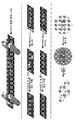
도 1은 본 개시의 일부 실시예들에 따른 열전 디바이스(100)를 도시한다. 열전 디바이스(100)는, 열전 디바이스(100)의 전극들(103)의 제 1 세트와 전극들(104)의 제 2 세트 사이에 배치된 n-형(101) 및 p-형(102) 엘러먼트들을 포함한다. 예시된 바와 같이, 전극들(103)의 제 1 세트는 인접한 n-형(101) 및 p-형 엘러먼트들을 연결한다. Figure 1 illustrates a
전극들(103 및 104)은 각기 뜨거운 측의 재료(105) 및 차가운 측의 재료(106)와 접촉한다. 일부 실시예들에 있어서, 뜨거운 측의 재료(105) 및 차가운 측의 재료(106)는 전기적으로는 절연성이지만 열적으로 전도성이다. 전극들(103 및 104)에 대한 전기적 전위의 인가는 전류의 흐름을 야기하며, 이는 열전 디바이스(100)에 걸친 온도 구배(ΔT)를 생성한다. 온도 구배(ΔT)는 뜨거운 측의 재료(105)에서의 제 1 온도 (평균) T1로부터 차가운 측의 재료(106)에서의 제 2 온도 (평균) T2까지 걸쳐지며, 여기에서 T1 > T2이다. 온도 구배는 가열 및 냉각 목적들을 위해 사용될 수 있다. The
열전 디바이스(100)의 n-형(101) 및 p-형(102) 엘러먼트들은, 예를 들어, 나노구조체들과 같은 나노미터 내지 마이크로미터의 치수들을 갖는 구조체들로 형성될 수 있다. 일부 상황들에 있어서, 나노구조체들은 홀들의 어레이(즉, 메시)로 제공될 수 있는 홀들 또는 포함체들이다. 다른 상황들에 있어서, 나노구조체들은 나노와이어들과 같은 로드-형 구조체들이다. 일부 경우들에 있어서, 로드-형 구조체들은 서로 측방으로 분리된다. The n-
일부 경우들에 있어서, n-형(101) 및/또는 p-형(102) 엘러먼트들은 온도 구배의 방향을 따라 배향된 와이어들 또는 홀들의 어레이로 형성된다. 즉, 와이어들이 전극들(103)의 제 1 세트로부터 전극들(104)의 제 2 세트로 연장한다. 다른 경우들에 있어서, n-형(101) 및/또는 p-형(102) 엘러먼트들은, 온도 구배에 대하여 약 0° 내지 90° 사이의 각진 방향을 따라 배향된 홀들의 어레이로 형성된다. 일 예에 있어서, 홀들의 어레이는 온도 구배에 대하여 직각이다. 일부 경우들에 있어서, 홀들 또는 와이어들은 대략 나노미터들 내지 마이크로미터들의 치수들을 갖는다. 일부 경우들에 있어서, 홀들이 나노메시를 획정(define)할 수 있다. In some cases, the n-
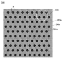
도 2는 본 개시의 일 실시예에 따른 홀들(원으로 둘러싸인 선택 홀들)의 어레이(201)를 갖는 열전 엘러먼트(200)의 개략적인 사시도이다. 홀들의 어레이는 본원에서 "나노메시"로서 지칭될 수 있다. 도 3 및 도 4는 열전 엘러먼트(200)의 원경 평면도 및 측면도이다. 엘러먼트(200)는 본원의 다른 곳에서 설명되는 바와 같은 n-형 또는 p-형 엘러먼트일 수 있다. 홀들의 어레이(201)는, 몇 나노미터 또는 그 미만으로부터 마이크론들, 밀리미터들, 또는 그 이상까지의 폭들을 가질 수 있는 개별적인 홀들(201a)을 포함한다. 일부 실시예들에 있어서, 홀들은 약 1 nm 내지 500 nm, 또는 5 nm 내지 100 nm, 또는 10 nm 내지 30 nm 사이의 폭들(또는, 원형인 경우 직경들)("d")을 갖는다. 홀들은 약 수 나노미터 또는 그 미만으로부터 마이크론들, 밀리미터들 또는 그 이상까지의 길이들("L")을 가질 수 있다. 일부 실시예들에 있어서, 홀들은 약 0.5 마이크론 내지 1 센티미터, 또는 1 마이크론 내지 500 밀리미터, 또는 10 마이크론 내지 1 밀리미터 사이의 길이들을 갖는다. Figure 2 is a schematic perspective view of a
홀들(201a)은 기판(200a) 내에 형성된다. 일부 경우들에 있어서, 기판(200a)은, 예를 들어, 탄소(예를 들어, 흑연 또는 그래핀(graphene)), 실리콘, 게르마늄, 비화 갈륨, 비화 알루미늄 갈륨, 실리사이드들, 실리콘 게르마늄, 비스무트 텔루라이드, 납 텔루라이드, 산화물들(예를 들어, SiOx, 여기에서 'x'는 0보다 더 큰 수), 질화 갈륨, 및 텔루륨 은 게르마늄 안티모니(tellurium silver germanium antimony; TAGS) 함유 합금들과 같은 고체 상태 재료이다. 예를 들어, 기판(200a)은 IV 족 재료(예를 들어, 실리콘 또는 게르마늄) 또는 III-V 족 재료(예를 들어, 비화 갈륨)일 수 있다. 기판(200a)은 하나 이상의 반도체들을 포함하는 반도체 재료로 형성될 수 있다. 반도체 재료는 각기 n-형 또는 p-형 엘러먼트들을 위하여 도핑된 n-형 또는 p-형일 수 있다.
일부 경우들에 있어서, 홀들(201a)은, He, Ne, Ar, N2, H2, CO2, O2, 또는 이들의 조합과 같은 가스로 충전된다. 다른 경우들에 있어서, 홀들(201a)은 진공 하에 존재한다. 대안적으로, 홀들은 반도체 재료, 절연(또는 유전체) 재료, 또는 가스(예를 들어, He, Ar, H2, N2, CO2)로 충전(예를 들어, 부분적으로 충전 또는 완전히 충전)될 수 있다. In some cases, the holes (201a) is then filled with He, Ne, Ar, N 2, H 2, CO 2, O 2, or a gas such as a combination of the two. In other cases, the
엘러먼트(200)의 제 1 단부(202) 및 제 2 단부(203)는 실리콘 또는 실리사이드와 같은 반도체-함유 재료를 갖는 기판과 접촉할 수 있다. 기판은 각각의 단부(202 및 203) 상에 전극에 대한 전기적 접촉부를 제공함에 있어서 보조할 수 있다. 대안적으로, 기판이 배제될 수 있으며, 제 1 단부(202) 및 제 2 단부(203)가 각기 제 1 전극(미도시) 및 제 2 전극(미도시)과 접촉할 수 있다. The
일부 실시예들에 있어서, 홀들(201a)은 실질적으로 단분산성이다. 단분산성 홀들은 실질적으로 동일한 크기, 형상 및/또는 분포(예를 들어, 단면 분포)를 가질 수 있다. 다른 실시예들에 있어서, 홀들(201a)은 다양한 크기들의 홀들의 영역들 내에 분포될 수 있으며, 그 결과 홀들(201a)이 반드시 단분산성은 아니다. 예를 들어, 홀들(201a)이 다분산성일 수 있다. 다분산성 홀들은, 서로 적어도 약 0.1%, 0.5%, 1%, 2%, 3%, 4%, 5%, 10%, 15%, 20%, 30%, 40%, 또는 50%만큼의 편차를 갖는 형상들, 크기들 및/또는 배향들을 가질 수 있다. 일부 상황들에 있어서, 디바이스(200)는 제 1 직경을 갖는 홀들의 제 1 세트 및 제 2 직경을 갖는 홀들의 제 2 세트를 포함한다. 제 1 직경은 제 2 직경보다 더 크다. 다른 경우들에 있어서, 디바이스(200)는 상이한 직경들을 갖는 홀들의 2개 이상의 세트들을 포함한다. In some embodiments, the
홀들(201a)은 다양한 패킹(packing) 배열들을 가질 수 있다. 일부 경우들에 있어서, 홀들(201a)은, 상단으로부터 보여질 때(도 3 참조), 육방 밀집(hexagonal close)-패킹 배열을 갖는다.
일부 실시예들에 있어서, 홀들의 어레이(201) 내의 홀들(201a)은 약 1 nm 내지 500 nm, 또는 5 nm 내지 100 nm, 또는 10 nm 내지 30 nm 사이의 중심-대-중심 간격을 갖는다. 일부 경우들에 있어서, 중심-대-중심 간격은 동일하며, 이는 단분산성 홀들(201a)에 대해서 그러할 수 있다. 다른 경우들에 있어서, 중심-대-중심 간격은 다양한 직경들 및/또는 배열들을 갖는 홀들의 그룹들에 대하여 상이할 수 있다. In some embodiments, the
홀들(201)의 치수들(길이들, 폭들) 및 패킹 배열, 및 엘러먼트(200)의 재료 및 도핑 구성(예를 들어, 도핑 농도)는 엘러먼트(200)를 갖는 열전 디바이스 및 엘러먼트(200)의 미리 결정된 전기적 전도율 및 열적 전도율에 영향을 주도록 선택될 수 있다. 예를 들어, 홀들(201)의 직경들 및 패킹 구성은 열적 전도율을 최소화하도록 선택될 수 있으며, 도핑 농도는 엘러먼트(200)의 전기적 전도율을 최대화하도록 선택될 수 있다. The dimensions (lengths, widths) and packing arrangements of the
기판(200a)의 도핑 농도는 적어도 약 1018 cm-3, 1019 cm-3, 1020 cm-3, 또는 1021 cm-3일 수 있다. 일부 예들에 있어서, 도핑 농도는 약 1018 내지 1021 cm-3, 또는 1019 내지 1020 cm-3이다. 도핑 농도는 열전 엘러먼트로서 사용하기에 적절한 저항률을 제공하도록 선택될 수 있다. 기판(200a)의 저항률은 적어도 약 0.001 ohm-cm, 0.01 ohm-cm, 또는 0.1 ohm-cm일 수 있거나, 일부 경우들에 있어서 약 1 ohm-cm, 0.5 ohm-cm, 0.1 ohm-cm 이하일 수 있다. 일부 예들에 있어서, 기판(200a)의 저항률은 약 0.001 ohm-cm 내지 1 ohm-cm, 0.001 ohm-cm 내지 0.5 ohm-cm, 또는 0.001 ohm-cm 내지 0.1 ohm-cm이다.The doping concentration of the
홀들의 어레이(201)는, 적어도 약 1.5:1, 또는 2:1, 또는 5:1, 또는 10:1, 또는 20:1, 또는 50:1, 또는 100:1, 또는 1000:1, 또는 5,000:1, 또는 10,000:1, 또는 100,000:1, 또는 1,000,000:1, 또는 10,000,000:1, 또는 100,000,000:1, 또는 그 이상의 종횡비(예를 들어, 개별적인 홀(201a)의 폭으로 나눈 엘러먼트(200)의 길이)를 가질 수 있다. The array of
홀들(201)은 정돈될 수 있으며 균일한 크기들 및 분포들을 가질 수 있다. 대안예로서, 홀들(201)이 정돈되지 않을 수 있고 균일한 분포를 갖지 않을 수 있다. 예를 들어, 홀들(201)은, 홀들(201)의 패턴에 대한 장거리 질서가 존재하지 않도록 무질서화될 수 있다.
일부 실시예들에 있어서, 열전 엘러먼트들은 와이어들의 어레이를 포함할 수 있다. 와이어들의 어레이는, 예를 들어, 로드-형 구조체들인 개별적인 와이어들을 포함할 수 있다. In some embodiments, the thermoelectric elements may comprise an array of wires. The array of wires may comprise individual wires, for example, rod-like structures.
엘러먼트(200)의 홀들의 어레이에 대한 대안예로서, 홀들이 정돈되지 않을 수 있고 균일한 분포를 갖지 않을 수 있다. 일부 예들에 있어서, 홀들에 대하여 장거리 질서가 존재하지 않는다. 일부 경우들에 있어서, 홀들이 랜덤한 방향들에서 서로 교차할 수 있다. 홀들은 교차 홀들, 예컨대 다양한 방향들로 홀들로부터 돌출하는 2차 홀들을 포함할 수 있다. 2차 홀들은 추가적인 2차 홀들을 가질 수 있다. 홀들은 다양한 크기들을 가질 수 있으며, 랜덤하고 균일하지 않을 수 있는 다양한 방향들을 따라 정렬될 수 있다. As an alternative to the array of holes in
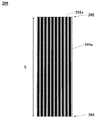
도 5는 본 개시의 일 실시예에 따른 열전 엘러먼트(500)의 개략적인 상단 사시도이다. 도 6은 열전 엘러먼트(500)의 개략적인 사시 평면도이다. 열전 엘러먼트(500)는 본원에서 제공되는 디바이스들, 시스템들 및 방법들과 함께 사용될 수 있다. 엘러먼트(500)는 개별적인 와이어들(501a)을 갖는 와이어들의 어레이(501)를 포함한다. 일부 실시예들에 있어서, 와이어들은 약 1 nm 내지 500 nm, 또는 5 nm 내지 100 nm, 또는 10 nm 내지 30 nm 사이의 폭들(또는, 원형인 경우 직경들)("d")을 갖는다. 와이어들들은 약 수 나노미터 또는 그 미만으로부터 마이크론들, 밀리미터들 또는 그 이상까지의 길이들("L")을 가질 수 있다. 일부 실시예들에 있어서, 와이어들은 약 0.5 마이크론 내지 1 센티미터, 또는 1 마이크론 내지 500 밀리미터, 또는 10 마이크론 내지 1 밀리미터 사이의 길이들을 갖는다. 5 is a schematic top perspective view of a
일부 실시예들에 있어서, 와이어들(501a)은 실질적으로 단분산성이다. 단분산성 와이어들은 실질적으로 동일한 크기, 형상 및/또는 분포(예를 들어, 단면 분포)를 가질 수 있다. 다른 실시예들에 있어서, 와이어들(501a)은 다양한 크기들의 홀들의 영역들 내에 분포될 수 있으며, 그 결과 와이어들(501a)이 반드시 단분산성은 아니다. 예를 들어, 와이어들(501a)이 다분산성일 수 있다. 다분산성 와이어들은, 서로 적어도 약 0.1%, 0.5%, 1%, 2%, 3%, 4%, 5%, 10%, 15%, 20%, 30%, 40%, 또는 50%만큼의 편차를 갖는 형상들, 크기들 및/또는 배향들을 가질 수 있다. In some embodiments, the
일부 실시예들에 있어서, 와이어들의 어레이(501) 내의 와이어들(501a)은 약 1 nm 내지 500 nm, 또는 5 nm 내지 100 nm, 또는 10 nm 내지 30 nm 사이의 중심-대-중심 간격을 갖는다. 일부 경우들에 있어서, 중심-대-중심 간격은 동일하며, 이는 단분산성 와이어들(501a)에 대해서 그러할 수 있다. 다른 경우들에 있어서, 중심-대-중심 간격은 다양한 직경들 및/또는 배열들을 갖는 와이어들의 그룹들에 대하여 상이할 수 있다. In some embodiments, the
일부 경우들에 있어서, 와이어들(501a)은, 예를 들어, 실리콘, 게르마늄, 비화 갈륨, 비화 알루미늄 갈륨, 실리사이드 합금들, 실리콘 게르마늄의 합금들, 비스무트 텔루라이드, 납 텔루라이드, 산화물들(예를 들어, SiOx, 여기에서 'x'는 0보다 더 큰 수), 질화 갈륨, 및 텔루륨 은 게르마늄 안티모니(TAGS) 함유 합금들과 같은 반도체 재료와 같은 고체 상태 재료로 형성된다. 와이어들(501a)은 본원에 개시되는 다른 재료들로 형성될 수 있다. 와이어들(501a)은 n-형 도펀트 또는 p-형 도펀트로 도핑될 수 있다. 반도체 재료의 도핑 농도는 적어도 약 1018 cm-3, 1019 cm-3, 1020 cm-3, 또는 1021 cm-3일 수 있다. 일부 예들에 있어서, 도핑 농도는 약 1018 내지 1021 cm-3, 또는 1019 내지 1020 cm-3이다. 반도체 재료의 도핑 농도는 열전 엘러먼트로서 사용하기에 적절한 저항률을 제공하도록 선택될 수 있다. 반도체 재료의 저항률은 적어도 약 0.001 ohm-cm, 0.01 ohm-cm, 또는 0.1 ohm-cm일 수 있거나, 일부 경우들에 있어서 약 1 ohm-cm, 0.5 ohm-cm, 0.1 ohm-cm 이하일 수 있다. 일부 예들에 있어서, 반도체 재료의 저항률은 약 0.001 ohm-cm 내지 1 ohm-cm, 0.001 ohm-cm 내지 0.5 ohm-cm, 또는 0.001 ohm-cm 내지 0.1 ohm-cm이다. In some cases, the
일부 실시예들에 있어서, 와이어들(501a)이 엘러먼트(500)의 제 1 단부(502) 및 제 2 단부(503)에서 반도체 기판들에 부착된다. 반도체 기판들은 개별적인 와이어들(501a)의 n-형 또는 p-형 도핑 구성을 가질 수 있다. 다른 실시예들에 있어서, 제 1 단부(502) 및 제 2 단부(503)에서 와이어들(501a)이 반도체 기판들에 부착되는 것이 아니라, 전극들에 부착될 수 있다. 예를 들어, 제 1 전극(미도시)이 제 1 단부(502)와 전기적으로 접촉할 수 있으며, 제 2 전극이 제 2 단부(503)와 전기적으로 접촉할 수 있다. In some embodiments,
도 6을 참조하면, 와이어들(501a) 사이의 공간(504)이 진공 또는 다양한 재료들로 충전될 수 있다. 일부 실시예들에 있어서, 와이어들은, 이산화 실리콘, 이산화 게르마늄, 산화 갈륨 비소, 스핀 온 글래스(spin on glass), 및 예를 들어, 화학적 기상 증착 또는 원자 층 증착과 같은 기체 상 증착을 사용하여 증착되는 다른 절연체들과 같은, 전기적인 절연 재료에 의해 서로로부터 측방으로 분리된다. 다른 실시예들에 있어서, 와이어들은, He, Ne, Ar, N2, H2, CO2, O2, 또는 이들의 조합과 같은 가스 또는 진공에 의해 서로로부터 측방으로 분리된다. Referring to FIG. 6, a
와이어들의 어레이(501)는, 적어도 약 1.5:1, 또는 2:1, 또는 5:1, 또는 10:1, 또는 20:1, 또는 50:1, 또는 100:1, 또는 1000:1, 또는 5,000:1, 또는 10,000:1, 또는 100,000:1, 또는 1,000,000:1, 또는 10,000,000:1, 또는 100,000,000:1, 또는 그 이상의 종횡비-예를 들어, 개별적인 와이어(501a)의 폭으로 나눈 엘러먼트(500)의 길이-를 가질 수 있다. 일부 경우들에 있어서, 엘러먼트(500)의 길이 및 개별적인 와이어(501a)의 길이는 실질적으로 동일하다. The array of
본원에서 제공되는 열전 엘러먼트들은, 냉각 및/또는 가열에서의 사용을 위하여, 그리고 일부 경우들에 있어서 전력 생성에서의 사용을 위하여 열전 디바이스들 내에 통합될 수 있다. 일부 예들에 있어서, 디바이스(100)는 전력 생성 디바이스로서 사용될 수 있다. 일 예에 있어서, 디바이스(100)는, 디바이스(100)의 전극들 및 열전 엘러먼트들에 걸쳐 온도 구배를 제공함으로써 전력 생성을 위해 사용된다. The thermoelectric elements provided herein may be incorporated into thermoelectric devices for use in cooling and / or heating, and in some cases for use in power generation. In some examples, the
엘러먼트(500)의 와이어들의 어레이에 대한 대안예로서, 와이어들이 정돈되지 않을 수 있고 균일한 분포를 갖지 않을 수 있다. 일부 예들에 있어서, 와이어들에 대하여 장거리 질서가 존재하지 않는다. 일부 경우들에 있어서, 와이어들이 랜덤한 방향들에서 서로 교차할 수 있다. 와이어들은 다양한 크기들을 가질 수 있으며, 랜덤하고 균일하지 않을 수 있는 다양한 방향들을 따라 정렬될 수 있다. As an alternative to the array of wires of
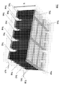
도 7은 본 개시의 일 실시예에 따른 n-형 엘러먼트들(701) 및 p-형 엘러먼트들(702)을 갖는 열전 디바이스(700)를 도시한다. n-형 엘러먼트들(701) 및 p-형 엘러먼트들(702) 각각이 나노와이어들과 같은 와이어들의 어레이를 포함한다. 와이어들의 어레이는 복수의 와이어들을 포함할 수 있다. n-형 엘러먼트들(701)은 n-형(또는 n-도핑된) 와이어들을 포함하며, p-형 엘러먼트들(702)은 p-형 와이어들을 포함한다. 와이어들은 나노와이어들 또는 다른 로드-형 구조체들일 수 있다. FIG. 7 illustrates a
인접한 n-형 엘러먼트들(701) 및 p-형 엘러먼트들(702)이 전극들(703 및 704)을 사용하여 그들의 단부에서 서로 전기적으로 연결된다. 디바이스(700)는 엘러먼트들(701 및 702)의 대향되는 단부들에서 제 1 열 전도성 전기 절연성 층(705) 및 제 2 열 전도성 전기 절연성 층(706)을 포함한다. Adjacent n-
디바이스(700)는 전극들(703 및 704)과 전기적으로 연통하는 단자들(707 및 708)을 포함한다. 단자들(707 및 708)에 걸친 전기적 전위의 인가는 각기 n-형 및 p-형 엘러먼트들(701 및 702) 내의 전자들 및 홀들의 흐름을 생성하며, 이는 엘러먼트들(701 및 702)에 걸친 온도 구배를 생성한다. 제 1 열 전도성 전기 절연성 층(705)은 디바이스(700)의 차가운 측이며; 제 2 열 전도성 전기 절연성 층(706)은 디바이스(700)의 뜨거운 측이다. 차가운 측은 뜨거운 측보다 더 차갑다(즉, 더 낮은 동작 온도를 갖는다).
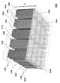
도 8은 본 개시의 일 실시예에 따른 n-형 엘러먼트들(801) 및 p-형 엘러먼트들(802)을 갖는 열전 디바이스(800)를 도시한다. n-형 엘러먼트들(801) 및 p-형 엘러먼트들(802)은 각기 n-형 및 p-형 반도체 기판들 내에 형성된다. 각각의 기판은 나노홀들과 같은 홀들의 어레이를 포함할 수 있다. 홀들의 어레이는 복수의 홀들을 포함할 수 있다. 개별적인 홀은 n-형 또는 p-형 엘러먼트의 길이에 걸쳐 이어질 수 있다. 홀들은 단분산성일 수 있으며, 이러한 경우에 있어서 홀 치수들 및 중심-대-중심 간격이 실질적으로 일정할 수 있다. 일부 경우들에 있어서, 홀들의 어레이는 상이할 수 있는 중심-대-중심 간격 및 홀 치수들(예를 들어, 폭들 또는 직경들)을 갖는 홀들을 포함한다. 이러한 경우에 있어서, 홀들은 단분산성이 아닐 수 있다. FIG. 8 illustrates a
선택 n-형 엘러먼트들(801) 및 p-형 엘러먼트들(802)이 전극들(803 및 804)에 의해 그들의 단부에서 서로 전기적으로 연결된다. 디바이스(800)는 엘러먼트들(801 및 802)의 대향되는 단부들에서 제 1 열 전도성 전기 절연성 층("제 1 층")(805) 및 제 2 열 전도성 전기 절연성 층("제 2 층)(806)을 포함한다. The selection n-
디바이스(800)는 전극들(803 및 804)과 전기적으로 연통하는 단자들(807 및 808)을 포함한다. 단자들(807 및 808)에 걸친 전기적 전위의 인가는 각기 n-형 및 p-형 엘러먼트들(801 및 802) 내의 전자들 및 홀들의 흐름을 생성하며, 이는 엘러먼트들(801 및 802)에 걸친 온도 구배를 생성한다. 제 1 열 전도성 전기 절연성 층(805)은 디바이스(800)의 차가운 측이며; 제 2 열 전도성 전기 절연성 층(806)은 디바이스(800)의 뜨거운 측이다. 차가운 측은 뜨거운 측보다 더 차갑다(즉, 더 낮은 동작 온도를 갖는다).
열전 디바이스(800)는 제 2 열 전도성 전기 절연성 층(806)으로부터 제 1 열 전도성 전기 절연성 층(805)으로의 온도 구배를 갖는다. 일부 경우들에 있어서, 홀들은 제 1 층(805)으로부터 제 2 층(806)까지 배향된 벡터에 평행하게 배치된다. 다른 경우들에 있어서, 홀들은 벡터에 대하여 0°보다 더 큰 각도로 배치된다. 예를 들어, 홀들은 벡터에 대하여 적어도 약 1°, 10°, 20°, 30°, 40°, 50°, 60°, 70°, 80°, 또는 90°의 각도로 배치될 수 있다. The
도 9는, 엘러먼트들이 n-형 및 p-형 엘러먼트들의 기판 내에 형성된 홀들을 갖는, n-형 엘러먼트들(901) 및 p-형 엘러먼트들(902)을 갖는 열전 디바이스(900)를 도시한다. 홀들은 디바이스(900)의 전극들(903 및 904)에 직각인 벡터("V")에 수직으로 배향된다. 9 shows a
본원에서 제공되는 열전 엘러먼트들의 와이어들 또는 홀들은 기판 내에 형성될 수 있으며 전극과 같은 지지 구조체에 실질적으로 역-평행하게(anti-parallel) 배향될 수 있다. 일부 예들에 있어서, 와이어들 또는 홀들은 지지 구조체에 대하여 0°, 또는 10°, 또는 20°, 또는 30°, 또는 40°, 또는 50°, 또는 60°, 또는 70°, 또는 80°, 또는 85°보다 더 큰 각도로 배향된다. 일 예에 있어서, 와이어들 또는 홀들은 지지 구조체에 대하여 약 90°의 각도로 배향된다. 전극은 열전 디바이스의 전극일 수 있다. 일부 경우들에 있어서, 와이어들 또는 홀들은 전극에 실질적으로 평행하게 배향될 수 있다. The wires or holes of the thermoelectric elements provided herein can be formed in the substrate and can be oriented anti-parallel substantially to a support structure such as an electrode. In some instances, the wires or holes may be at a 0 [deg.], Or 10 [deg.], Or 20 [deg.], Or 30 [deg.], Or 40 [deg.], Or 50 [deg.], Or 60 [deg. Lt; RTI ID = 0.0 > 85 < / RTI > In one example, the wires or holes are oriented at an angle of about 90 relative to the support structure. The electrode may be an electrode of the thermoelectric device. In some cases, the wires or holes may be oriented substantially parallel to the electrodes.
도 7 내지 도 9의 디바이스들에 대한 대안예로서, 열전 디바이스는, 상이한 크기들 및/또는 분포들을 가질 수 있는 개별적인 홀들 또는 와이어들을 갖는 홀들 또는 와이어들의 어레이를 갖는 열전 엘러먼트를 가질 수 있다. 홀들 또는 와이어들의 어레이가 정돈되지 않을 수 있고 균일한 분포를 갖지 않을 수 있다. 일부 예들에 있어서, 홀들 또는 와이어들에 대하여 장거리 질서가 존재하지 않는다. 일부 경우들에 있어서, 홀들 또는 와이어들이 랜덤한 방향들에서 서로 교차할 수 있다. 홀들 또는 와이어들은 교차 홀들 또는 와이어들, 예컨대 다양한 방향들로 다른 홀들 또는 와이어들로부터 돌출하는 2차 홀들 또는 와이어들을 포함할 수 있다. 홀들 또는 와이어들은 다양한 크기들을 가질 수 있으며, 랜덤하고 균일하지 않을 수 있는 다양한 방향들을 따라 정렬될 수 있다. 다른 대안예로서, 열전 디바이스는, 홀들 또는 와이어들의 정돈된 어레이를 갖는 적어도 하나의 열전 엘러먼트(p 또는 n-형), 및 홀들 또는 와이어들의 무질서한 어레이를 갖는 적어도 하나의 열전 엘러먼트(p 또는 n-형)를 포함할 수 있다. 홀들 또는 와이어들의 무질서한 어레이는, 정돈되지 않고 균일한 분포를 갖지 않는 홀들 또는 와이어들을 포함할 수 있다. As an alternative to the devices of Figs. 7-9, a thermoelectric device may have thermoelectric elements having arrays of holes or wires with individual holes or wires that may have different sizes and / or distributions. The array of holes or wires may not be arranged and may not have a uniform distribution. In some instances, there is no long range order for holes or wires. In some cases, the holes or wires may cross each other in random directions. The holes or wires may include intersecting holes or wires, e.g., secondary holes or wires that protrude from other holes or wires in various directions. The holes or wires may have various sizes and may be aligned along various directions that may be random and non-uniform. As another alternative, the thermoelectric device can include at least one thermoelectric element (p or n-type) having an ordered array of holes or wires, and at least one thermoelectric element (p or n-type) having a disordered array of holes or wires n-type). The disordered array of holes or wires may include holes or wires that are not tidy and have no uniform distribution.
본 개시의 홀 또는 와이어는 최적화된 열전 디바이스 성능에 적절한 표면 거칠기를 가질 수 있다. 일부 경우들에 있어서, 홀 또는 와이어의 제곱 평균 거칠기는 약 0.1 nm 내지 50 nm, 또는 1 nm 내지 20 nm, 또는 1 nm 내지 10 nm 사이이다. 거칠기는, 투과 전자 현미경검사(TEM) 또는, 원자력 현미경검사(atomic force microscopy; AFM) 또는 주사 터널링 현미경검사(scanning tunneling microscopy; STM)와 같은 다른 표면 분석 기술에 의해 결정될 수 있다. 표면 거칠기는 표면 주름(surface corrugation)에 의해 특징지어질 수 있다. The holes or wires of the present disclosure may have surface roughness suitable for optimized thermoelectric device performance. In some cases, the square mean roughness of the hole or wire is between about 0.1 nm and 50 nm, or between 1 nm and 20 nm, or between 1 nm and 10 nm. Roughness can be determined by other surface analysis techniques such as transmission electron microscopy (TEM) or atomic force microscopy (AFM) or scanning tunneling microscopy (STM). Surface roughness can be characterized by surface corrugation.
열전 엘러먼트들을 형성하기 위한 방법들 Methods for forming thermoelectric elements
본 개시는 열전 엘러먼트들을 형성하기 위한 다양한 방법들을 제공한다. 열전 엘러먼트는 전기화학적 에칭을 사용하여 형성될 수 있다. 일부 경우들에 있어서, 열전 엘러먼트는 캐소드(cathodic) 또는 애노드 에칭(anodic etching)에 의해 형성되며, 일부 경우들에 있어서 촉매를 사용하지 않고 형성된다. 열전 엘러먼트는 금속성 촉매들을 사용하지 않고 형성될 수 있다. 열전 엘러먼트는, 에칭될 기판의 표면 상에 금속성 코팅을 제공하지 않고 형성될 수 있다. 이는 또한, 순수하게 전기화학적 애노드 에칭 및 적절한 에칭 용액들 및 전해액들을 사용하여 수행될 수 있다. 대안예로서, 열전체는, 예를 들어, 이들의 각각이 전체적으로 본원에 참조로서 통합되는, 2012년 07월 17일자로 출원된 PCT/US2012/047021호, 2013년 01월 17일자로 출원된 PCT/US2013/021900호, 2013년 08월 16일자로 출원된 PCT/US2013/055462호, 2013년 10월 29일자로 출원된 PCT/US2013/067346호에서 설명되는 바와 같이, 적절한 에칭 용액들 및 전해액들 내에서 금속 촉매 전기화학적 에칭을 사용하여 형성될 수 있다. The present disclosure provides various methods for forming thermoelectric elements. The thermoelectric element can be formed using electrochemical etching. In some cases, the thermoelectric elements are formed by cathodic or anodic etching, and in some cases are formed without the use of a catalyst. The thermoelectric element can be formed without using metallic catalysts. The thermoelectric element can be formed without providing a metallic coating on the surface of the substrate to be etched. It can also be performed using purely electrochemical anode etching and suitable etching solutions and electrolytes. As an alternative, the entire row may be formed, for example, in PCT / US2012 / 047021, filed July 17, 2012, PCT, filed January 17, 2013, each of which is incorporated herein by reference in its entirety. As described in PCT / US2013 / 021900, PCT / US2013 / 055462 filed on August 16, 2013, and PCT / US2013 / 067346 filed October 29, 2013, suitable etch solutions and electrolytes RTI ID = 0.0 > electrochemical < / RTI >
열전 엘러먼트들을 형성하기 위하여 촉매들을 사용하지 않는 것에 대한 다양한 이점들이 본원에서 인식된다. 일 예에 있어서, 비-금속 촉매 에칭은, 에칭 이후 열전 엘러먼트로부터 금속 촉매들을 제거하기 위한 세정(cleanup) 단계들을 포함하여 금속(또는 금속성) 촉매들에 대한 필요성을 배제할 수 있으며, 이는 더 적은 프로세싱 단계들을 가능하게 할 수 있다. 금속 촉매들이 비쌀 수 있기 때문에, 이는 또한 감소된 제조 비용을 가능하게 할 수 있다. 금속 촉매들은, 희귀한 및/또는 비싼 금속성 재료들(예를 들어, 금, 은, 백금, 또는 팔라듐)을 포함할 수 있으며, 금속성 촉매의 사용을 제거하는 것이 바람직하게는 열전 엘러멘트들을 형성하는 비용을 감소시킬 수 있다. 추가적으로, 비-촉매 프로세스는 더 재현 가능하고 제어 가능할 수 있다. 일부 경우들에 있어서, 본원에서 설명되는 비-촉매 프로세스는 열전 엘러먼트들의 상대적으로 작은 생산 스케일로부터 열전 엘러먼트들의 상대적으로 더 큰 생산 스케일로 스케일링(scale)될 수 있다. Various advantages of not using catalysts to form thermoelectric elements are recognized herein. In one example, the non-metal catalytic etching can eliminate the need for metal (or metallic) catalysts, including cleanup steps to remove metal catalysts from the thermoelectric element after etching, Less processing steps may be possible. Because metal catalysts can be expensive, this can also enable reduced manufacturing costs. The metal catalysts may include rare and / or expensive metallic materials (e.g., gold, silver, platinum, or palladium), and it may be desirable to remove the use of metallic catalysts, preferably to form thermoelements The cost can be reduced. Additionally, non-catalytic processes may be more reproducible and controllable. In some cases, the non-catalytic process described herein can be scaled from a relatively small production scale of thermoelectric elements to a relatively larger production scale of thermoelectric elements.
본 개시는, 소비자 및 산업 애플리케이션들과 같은 다양한 애플리케이션들에서의 사용을 위한 열전 재료들을 형성하기 위한 방법들을 제공한다. 일부 예들에 있어서, 열전 재료들은 소비자 전자 디바이스들(예를 들어, 스마트 시계, 휴대용 전자 디바이스들, 및 건강/피트니스 추적 디바이스들)에서 사용된다. 다른 예로서, 본 개시의 열전 재료는 열 손실이 존재하는 위치에서와 같이 산업 환경에서 사용될 수 있으며, 이러한 열은 전력을 생성하기 위하여 포획되고 사용될 수 있다. The present disclosure provides methods for forming thermoelectric materials for use in a variety of applications such as consumer and industrial applications. In some instances, thermoelectric materials are used in consumer electronic devices (e.g., smart clocks, portable electronic devices, and health / fitness tracking devices). As another example, the thermoelectric materials of the present disclosure can be used in industrial environments, such as where heat loss is present, and such heat can be captured and used to generate power.
본 개시는 가요성 또는 실질적으로 가요성인 열전 재료들을 형성하기 위한 방법들을 제공한다. 가요성 재료는, 소성 변형 또는 파손을 경험하지 않고 측정 평면에 대하여 적어도 약 1°, 5°, 10°, 15°, 20°, 25°, 30°, 35°, 40°, 45°, 50°, 60°, 70°, 80°, 90°, 100°, 120°, 130°, 140°, 150°, 160°, 170°, 또는 180°의 각도로 굽혀지는 재료일 수 있다. 가요성 재료는 가요성 재료의 주어진 영역 위에 인가되는 힘(즉, 압력) 하에서 굽혀질 수 있다. 소성 변형은, 예를 들어, 3-점 테스팅(예를 들어, 인스트론 신장(instron extension)) 또는 인장 테스팅에 의해 측정될 수 있다. 이에 더하여 또는 대안예로서, 가요성 재료는, 3-점 테스팅(예를 들어, 인스트론 신장) 또는 인장 테스팅에 의해 측정되는 약 20%, 15%, 10%, 5%, 1%, 또는 0.1% 이하인 소성 변형에서, 측정 평면에 대하여 적어도 약 1°, 5°, 10°, 15°, 20°, 25°, 30°, 35°, 40°, 45°, 50°, 60°, 70°, 80°, 90°, 100°, 120°, 130°, 140°, 150°, 160°, 170°, 또는 180°의 각도로 굽혀지는 재료일 수 있다. 가요성 재료는 실질적으로 유연한 재료일 수 있다. 가요성 재료는 표면에 맞춰지거나 또는 이에 대하여 몰딩(mold)될 수 있는 재료일 수 있다. 이러한 재료들은, 소비자 및 산업 환경들과 같은 다양한 환경들에서의 사용을 위해 이용될 수 있다. 본원의 방법들에 따라 형성되는 열전 엘러먼트들은 다양한 형상들 및 구성들로 형성될 수 있다. 이러한 형상들은, 예컨대 주어진 물체에 맞추기 위하여 사용자에 의해 희망되는 바와 같이 변화될 수 있다. 열전 엘러먼트들은 제 1 형상을 가질 수 있으며, 형상 또는 구성으로 형성된 이후에 열전 엘러먼트들이 제 2 형상을 가질 수 있다. 열전 엘러먼트들은 제 2 형상으로부터 초기 형상으로 변환될 수 있다. The present disclosure provides methods for forming flexible or substantially flexible thermoelectric materials. The flexible material may be at least about 1 DEG, 5 DEG, 10 DEG, 15 DEG, 20 DEG, 25 DEG, 30 DEG, 35 DEG, 40 DEG, 45 DEG, or 50 DEG relative to the measurement plane without experiencing plastic deformation or breakage Or may be a material bent at an angle of 60, 70, 80, 90, 100, 120, 130, 140, 150, 160, 170 or 180 degrees. The flexible material may be bent under the force (i.e., pressure) applied over a given area of the flexible material. Plastic deformation can be measured, for example, by three-point testing (e.g., instron extension) or tensile testing. In addition, or as an alternative, the flexible material can be about 20%, 15%, 10%, 5%, 1%, or 0.1 (as measured by three-point testing %, 10, 15, 20, 25, 30, 35, 40, 45, 50, 60, 70 , 80 °, 90 °, 100 °, 120 °, 130 °, 140 °, 150 °, 160 °, 170 °, or 180 °. The flexible material may be a substantially flexible material. The flexible material can be a material that can fit on the surface or can be molded thereon. Such materials can be used for use in a variety of environments, such as consumer and industrial environments. The thermoelectric elements formed according to the methods herein can be formed in a variety of shapes and configurations. These shapes may be changed, for example, as desired by the user to fit into a given object. The thermoelectric elements may have a first shape and the thermoelectrons may have a second shape after being formed in shape or configuration. The thermoelectric elements can be converted from the second shape to the initial shape.
본 개시의 일 측면에 있어서, 열전 디바이스(또는 재료)는 애노드 에칭을 사용하여 형성된다. 애노드 에칭은, 에칭되는 기판에 대한 전기적 연결들, 기판과 접촉하는 에칭 용액들 또는 전해액들을 홀딩하기 위한 하나 이상의 저장소(reservoir)들, 및 에칭 프로세스의 분석적 측정들 및 모니터링을 위한 액세스(access)를 제공하는 전기화학적 에칭 셀(cell) 내에서 수행될 수 있다. 에칭 용액들 및/또는 전해액들은 수용성 용액을 포함할 수 있다. 에치(또는 에칭) 용액들 및/또는 전해액들은, 염기성, 중성, 또는 산성 용액일 수 있다. 에칭 용액들의 예들은, 불산(hydrofluoric acid; HF), 염산(hydrochloric acid; HCl), 브롬화 수소(hydrogen bromide; HBr), 요오드화 수소(hydrogen iodide; HI), 또는 이들의 조합들과 같은 산들을 포함한다. 에칭 용액들 및/또는 전해액들은 전기적으로 전도성 용액일 수 있다. 일 예에 있어서, 에칭 셀은 전해액을 포함하는 용액을 포함하는 상단 저장소를 포함한다. 상단 저장소는 에칭될 기판에 인접하여(예를 들어, 이의 상단 상에) 위치될 수 있다. 에칭될 기판은, 촉매성 재료들일 수 있는 하나 이상의 금속 재료들이 실질적으로 존재하지 않을 수 있다. 에칭될 기판은 금속성 코팅이 없을 수 있다. 일부 예들에 있어서, 에칭될 기판은, (예를 들어, 기판의 표면 상에) x-선 광전자 분광법(XPS)에 의해 측정되는 약 25%, 20%, 15%, 10%, 5%, 1%, 0.1%, 0.01%, 0.001%, 0.0001%, 0.00001%, 또는 000001%보다 더 작은 금속 함량을 갖는다. In one aspect of the present disclosure, a thermoelectric device (or material) is formed using an anode etch. The anode etch includes electrical connections to the substrate to be etched, one or more reservoirs for holding etching solutions or electrolytes in contact with the substrate, and access for monitoring and analytical measurements of the etching process Or in an electrochemical etch cell that provides an etchant. The etching solutions and / or the electrolytic solutions may comprise an aqueous solution. Etch (or etching) solutions and / or electrolytes may be a basic, neutral, or acidic solution. Examples of etching solutions include acids such as hydrofluoric acid (HF), hydrochloric acid (HCl), hydrogen bromide (HBr), hydrogen iodide (HI), or combinations thereof do. The etching solutions and / or electrolytes may be electrically conductive solutions. In one example, the etch cell comprises an upper reservoir containing a solution comprising an electrolyte. The top reservoir may be located adjacent to (e.g., on top of) the substrate to be etched. The substrate to be etched may be substantially free of one or more metallic materials that may be catalytic materials. The substrate to be etched may be free of a metallic coating. In some instances, the substrate to be etched may be about 25%, 20%, 15%, 10%, 5%, 1% (as measured by x-ray photoelectron spectroscopy %, 0.1%, 0.01%, 0.001%, 0.0001%, 0.00001%, or less than 000001%.
에칭 용액은 산(예를 들어, HF) 또는, (중량으로) 약 70%, 60%, 50%, 40%, 30%, 20% 또는 10% 이하인, 일부 경우들에 있어서는 약 1%, 10%, 20%, 또는 30%보다 더 큰 (중량 퍼센트로서 취해지는) 산들의 농도를 포함할 수 있다. 일부 예들에 있어서, 농도는 (중량으로) 약 1% 내지 60%, 또는 10% 내지 50%, 또는 20% 내지 45%이다. 에칭 용액의 나머지는 용매(예를 들어, 물) 및 첨가제, 예컨대 알콜, 카르복실 산, 케톤 및/또는 알데하이드를 포함할 수 있다. 일부 예들에 있어서, 첨가제는 메탄올, 에탄올, 이소프로판올, 또는 이들의 조합과 같은 알콜이다. 첨가제는, 무질서한 패턴을 갖는 홀들의 실질적으로 균일한 분포와 같은 본 개시의 열전 엘러먼트들에서 사용하기에 적절한 속성들을 갖는 나노구조체들(예를 들어, 홀들)을 형성하는 동안 더 낮은 전류 밀도들의 사용을 가능하게 할 수 있다. 첨가제는, 2개 이상의 홀들 사이의 간격의 증가된 제어와 같은 본 개시의 열전 엘러먼트들에서 사용하기에 적절한 속성들을 갖는 나노구조체들(예를 들어, 홀들)을 형성하는 동안 더 낮은 전류 밀도들의 사용을 가능하게 할 수 있다. 첨가제는, 최대한으로 약 5 nm의 2개 이상의 홀들 사이의 간격과 같은 본 개시의 열전 엘러먼트들에서 사용하기에 적절한 속성들을 갖는 나노구조체들(예를 들어, 홀들)을 형성하는 동안 더 낮은 전류 밀도들의 사용을 가능하게 할 수 있다. 첨가제는, 최대한으로 약 20 nm의 2개 이상의 홀들 사이의 간격과 같은 본 개시의 열전 엘러먼트들에서 사용하기에 적절한 속성들을 갖는 나노구조체들(예를 들어, 홀들)을 형성하는 동안 더 낮은 전류 밀도들의 사용을 가능하게 할 수 있다. 첨가제는, 최대한으로 약 100 nm의 2개 이상의 홀들 사이의 간격과 같은 본 개시의 열전 엘러먼트들에서 사용하기에 적절한 속성들을 갖는 나노구조체들(예를 들어, 홀들)을 형성하는 동안 더 낮은 전류 밀도들의 사용을 가능하게 할 수 있다. The etch solution may be an acid (e.g., HF) or about 1%, 10% (by weight), in some cases less than about 70%, 60%, 50%, 40%, 30%, 20% %, 20%, or greater than 30% (taken as weight percent) of the acids. In some instances, the concentration is (by weight) about 1% to 60%, or 10% to 50%, or 20% to 45%. The remainder of the etching solution may include a solvent (e.g., water) and additives such as an alcohol, a carboxylic acid, a ketone, and / or an aldehyde. In some examples, the additive is an alcohol such as methanol, ethanol, isopropanol, or combinations thereof. The additive may be added to form nanostructures (e. G., Holes) having properties that are suitable for use in the thermoelectric elements of the present disclosure, such as a substantially uniform distribution of holes with a disordered pattern, Can be used. The additives may be added to form nanostructures (e. G., Holes) having properties suitable for use in thermoelectric elements of the present disclosure, such as increased control of the spacing between two or more holes, Can be used. The additive may be added to form nanostructures (e. G., Holes) having properties suitable for use in the thermoelectric elements of the present disclosure, such as spacing between two or more holes of at most about 5 nm, Density < / RTI > The additive may be added to form nanostructures (e. G., Holes) having properties suitable for use in the thermoelectric elements of the present disclosure, such as spacing between two or more holes of at most about 20 nm, Density < / RTI > The additive may be selected to provide a lower current (e. G., Holes) while forming nanostructures (e. G., Holes) with properties suitable for use in the thermoelectric elements of the present disclosure, such as spacing between two or more holes of up to about 100 nm Density < / RTI >
전기적 전류는 에지(edge) 또는 후면(backside) 접촉부를 사용하여 기판으로 및/또는 기판을 통해, 그리고 용액/전해액을 통해, 그리고 상대 전극 내로 소싱(source)될 수 있다. 상대 전극은 상단 저장소와 전기적으로 연통할 수 있으며, 일부 경우들에 있어서 상단 저장소 내에 위치될 수 있다. 일부 경우들에 있어서, 상대 전극은 기판의 상단면에 인접하거나 또는 이와 접촉할 수 있다. 에칭 셀의 몸체는, 에칭 용액 또는 전해액에 대하여 비활성인 재료들(예를 들어, PTFE, PFA, 폴리프로필렌, HDPE)로 제조될 수 있다. 에지 또는 후면 접촉부는 기판 상의 금속 접촉부를 포함할 수 있거나, 또는 이는 적절한 전해액을 사용하는 액체 접촉부일 수 있다. 상대 전극은 적절한 전극 재료로 구성된 와이어 또는 메시를 포함할 수 있다. 에칭 셀은 용액 운동을 유지하기 위한 기계적인 패들(paddle)들 또는 초음파 교반기들을 포함할 수 있거나, 또는 전체 셀이 돌려지거나, 회전되거나 또는 흔들어질 수 있다. 일부 예들에 있어서, 에칭 이전에 및/또는 에칭 동안에 교반하는 것이 개선된 에칭 균일성을 가능하게 할 수 있다. 이는, 전해액이 에칭 동안 순환되는 것을 가능하게 할 수 있다. 다른 예에 있어서, 에칭 셀은, 하나 이상의 용액들/전해액들을 갖는 하나 이상의 재순환 저장소들 및 에칭 챔버들을 포함할 수 있다. The electrical current can be sourced into the substrate and / or through the substrate and through the solution / electrolyte and into the counter electrode using edge or backside contacts. The counter electrode may be in electrical communication with the top reservoir, and in some cases may be located within the top reservoir. In some cases, the counter electrode may be adjacent to or in contact with the top surface of the substrate. The body of the etch cell may be made of materials that are inert to the etch solution or electrolyte (e.g., PTFE, PFA, polypropylene, HDPE). The edge or back contact may comprise a metal contact on the substrate, or it may be a liquid contact using a suitable electrolyte. The counter electrode may comprise a wire or mesh comprised of a suitable electrode material. The etch cell may include mechanical paddles or ultrasonic agitators to maintain solution motion, or the entire cell may be turned, rotated, or shaken. In some instances, stirring before and / or during etching may enable improved etch uniformity. This may enable the electrolyte to be circulated during the etching. In another example, the etch cell may include one or more recirculation reservoirs and etch chambers having one or more solutions / electrolytes.
일 예에 있어서, 패턴화되지 않은 기판이 5개 이상에 이르는 전극 연결부들이 구비된 반응 공간 내로 로딩(load)된다. 전극들 중 하나(작업 전극)는 기판 후면과 오믹 접촉하며, 에칭제 전해액으로부터 격리된다. 전극들 중 하나(작업 전극)는 기판 후면과 오믹 접촉할 수 있으며, 에칭제 전해액과 접촉하지 않을 수 있다. 다른 전극(상대 전극)은 전해액 내에 잠기지만 기판과 직접 접촉하지 않을 수 있으며, 이는 전해액을 통해 기판 작업 전극으로 전류를 공급하기 위해 사용될 수 있다. 다른 전극(기준 전극)이 전해액 내에 침지되고 일부 경우들에 있어서 프리트(frit)를 사용하여 작업 전극 및 상대 전극 둘 모두로부터 격리되며, 이는 알려진 또는 미리 결정된 기준 표준을 사용하여 에칭 셀의 동작 전위를 센싱하기 위하여 사용된다. 다른 2개 이상의 전극들은 외부 전기장을 셋업하기 위하여 반응 공간 외부에 위치될 수 있다. 일부 경우들에 있어서, 적어도 2개의 전극들(작업 전극 및 상대 전극)이 요구된다. In one example, an unpatterned substrate is loaded into a reaction space having electrode connections of up to five or more. One of the electrodes (working electrode) is in ohmic contact with the backside of the substrate and is isolated from the etchant electrolyte. One of the electrodes (working electrode) may be in ohmic contact with the backside of the substrate and may not be in contact with the etchant electrolyte. The other electrode (counter electrode) may be immersed in the electrolyte but not in direct contact with the substrate, which may be used to supply current to the substrate working electrode through the electrolyte. Another electrode (reference electrode) is immersed in the electrolyte and in some cases is isolated from both the working electrode and the counter electrode using a frit, which can be used to determine the operating potential of the etch cell using known or predetermined reference standards It is used for sensing. The other two or more electrodes may be located outside the reaction space to set up an external electric field. In some cases, at least two electrodes (working electrode and counter electrode) are required.
반응 공간은 다수의 방식들로 사용될 수 있다. 하나의 접근방식에 있어서, 반응 공간은 애노드 전류를 기판 후면을 통해 적절한 전해액으로 전달함으로써 2-전극 구성에서 사용될 수 있다. 전해액은, 예를 들어, 물과 같은 희석제, 또는 불산과 같은 불소-함유 시약, 또는 과산화 수소와 같은 산화제를 포함하는 액체 혼합물일 수 있다. 전해액은 계면활성제들 및/또는 조절제(modifying agent)들을 포함할 수 있다. 작업 전위는 3-전극 구성에서 상대 전극을 사용하여 애노드 산화 동안 센싱될 수 있다. 애노드 산화는 반응 공간 외부에 위치된 전극들을 사용하여 DC 또는 AC 외부 필드가 존재하는 상태에서 수행될 수 있다. The reaction space can be used in a number of ways. In one approach, the reaction space can be used in a two-electrode configuration by transferring the anode current through the backside of the substrate to the appropriate electrolyte. The electrolytic solution can be, for example, a liquid mixture comprising a diluent such as water or a fluorine-containing reagent such as hydrofluoric acid, or an oxidizing agent such as hydrogen peroxide. The electrolytic solution may comprise surfactants and / or modifying agents. The working potential can be sensed during anode oxidation using a counter electrode in a three-electrode configuration. The anode oxidation can be performed in the presence of a DC or AC external field using electrodes located outside of the reaction space.
애노드 에칭 시에, 반도체의 전압/전류 보조 에칭은 전압/전류에 의존하는 레이트의 반도체의 에칭을 야기할 수 있다. 에칭 레이트, 에칭 깊이, 에칭 모폴로지(morphology), 공극 밀도, 공극 구조, 내부 표면적 및 표면 거칠기는, 전압/전류, 에칭 용액/전해액 조성 및 다른 첨가제들, 압력/온도, 전면/후면 조명, 및 뒤섞음/교반에 의해 제어될 수 있다. 이들은 또한, 반도체의 결정 배향, 도펀트 유형, 저항률(도핑 농도), 및 성장 프로세스(예를 들어, 플로트-존(float-zone) 또는 초크랄스키(Czochralski))에 의해 제어될 수 있다. 반도체의 저항률은 적어도 약 0.001 ohm-cm, 0.01 ohm-cm, 또는 0.1 ohm-cm일 수 있거나, 일부 경우들에 있어서 약 1 ohm-cm, 0.5 ohm-cm, 0.1 ohm-cm 이하일 수 있다. 일부 예들에 있어서, 반도체의 저항률은 약 0.001 ohm-cm 내지 1 ohm-cm, 0.001 ohm-cm 내지 0.5 ohm-cm, 또는 0.001 ohm-cm 내지 0.1 ohm-cm이다. At the anode etch, the voltage / current assisted etching of the semiconductor can cause etching of the semiconductor at a rate that depends on the voltage / current. Etch Rate, Etch Depth, Etch Morphology, Cavity Density, Cavity Structure, Internal Surface Area, and Surface Roughness, can be found in: voltage / current, etch solution / electrolyte composition and other additives, pressure / temperature, front / back lighting, / Stirring. They can also be controlled by crystal orientation of the semiconductor, dopant type, resistivity (doping concentration), and growth process (e.g., float-zone or Czochralski). The resistivity of the semiconductor can be at least about 0.001 ohm-cm, 0.01 ohm-cm, or 0.1 ohm-cm, or in some cases, less than about 1 ohm-cm, 0.5 ohm-cm and 0.1 ohm-cm. In some examples, the resistivity of the semiconductor is from about 0.001 ohm-cm to 1 ohm-cm, from 0.001 ohm-cm to 0.5 ohm-cm, or from 0.001 ohm-cm to 0.1 ohm-cm.
전압/전류 제어를 사용하는 반도체 기판의 에칭 동안, 전위 또는 바이어스(예를 들어, 직류 바이어스)가 아래에 있는 전극을 사용하여 기판에 인가된다. 이는 반도체 기판이 에칭되게끔 할 수 있다. 애노드 에칭의 결과로서, 반도체의 열 전도율이 상당히 떨어질 수 있다. 일부 예들에 있어서, 인가되는 바이어스를 이용함으로써, 공극률(질량 손실)이 제어되고 조율될 수 있으며, 그에 따라서 열적 및 전기적 속성들이 제어될 수 있다. 다른 예들에 있어서, 특정 에칭 용액/전해액 조성 및/또는 첨가제들을 이용함으로써 공극률이 제어될 수 있다. 또 다른 예들에 있어서, 이미 열거된 임의의 수의 변수들을 이용함으로써 공극율이 제어될 수 있다. During etching of a semiconductor substrate using voltage / current control, a potential or a bias (e.g., a DC bias) is applied to the substrate using the underlying electrode. This may cause the semiconductor substrate to be etched. As a result of the anode etch, the thermal conductivity of the semiconductor can be significantly reduced. In some instances, by using an applied bias, porosity (mass loss) can be controlled and tuned, and thermal and electrical properties can be controlled accordingly. In other examples, porosity can be controlled by using specific etching solution / electrolyte composition and / or additives. In yet other examples, porosity can be controlled by using any number of the variables already enumerated.
일부 경우들에 있어서 반도체 기판은 패턴화되지 않으며, 일부 경우들에 있어서 반도체 기판이 패턴화된다. 패턴화되지 않은 에칭 시에, 기판이 셀 내에서 직접적으로 에칭된다. 패턴화된 에칭 시에, 먼저 에칭을 방지하는 차단 층이 반도체 위에 위치되고, 그런 다음 특정 위치들에서 제거될 수 있다. 이러한 층은 적절한 임의의 방식(예를 들어, 화학 기상 증착, 스핀-코팅(spin-coating), 산화)으로 형성될 수 있으며, 그런 다음 후속 단계에서 희망되는 위치들에서 적절한 마스크(예를 들어, 포토리소그래피)를 사용하여 제거될 수 있다(예를 들어, 플라즈마 에칭, 반응성 이온 에칭, 스퍼터링(sputtering)). 대안적으로, 차단 층이 직접적으로 증착될 수 있다(예를 들어, 딥 펜 리소그래피(dip pen lithography), 잉크젯 프린팅, 스텐실을 통한 스프레이 코팅). 그 다음에, 차단 층 내의 패턴들의 네거티브 복제(negative replica)가 애노드 에칭 동안 기판 내로 전사된다. In some cases, the semiconductor substrate is not patterned, and in some cases the semiconductor substrate is patterned. Upon unpatterned etching, the substrate is etched directly in the cell. Upon patterned etching, a barrier layer that prevents etching first may be placed over the semiconductor and then removed at specific locations. Such a layer can be formed in any suitable manner (e.g., chemical vapor deposition, spin-coating, oxidation) and then transferred to a suitable mask (e.g., Photolithography) (e. G., Plasma etching, reactive ion etching, sputtering). Alternatively, the barrier layer can be deposited directly (e. G., Dip pen lithography, inkjet printing, spray coating through a stencil). A negative replica of the patterns in the blocking layer is then transferred into the substrate during the anode etch.
에칭은, 적절한 에칭 용액/전해액이 있는 상태에서 반도체 기판에 전기적 전위("전위")를 인가함으로써 수행될 수 있다. 전위는, 예를 들어, 접지와 같은 기준에 대하여 적어도 약 +0.01 V, +0.02 V, +0.03 V, +0.04 V, +0.05 V, +0.06 V, +0.07 V, +0.08 V, +0.09 V, +0.1 V, +0.2 V, +0.3 V, +0.4 V, +0.5 V, +0.6 V, +0.7 V, +0.8 V, +0.9 V, +1.0 V, +2.0 V, +3.0 V, +4.0 V, +5.0 V, +10 V, +20 V, +30 V, +40 V, 또는 +50 V일 수 있다. 일부 예들에 있어서, 전위는 기준에 대하여 약 +0.01 V 내지 +20 V, +0.1 V 내지 +10 V, 또는 +0.5 V 내지 +5 V이다. 일부 예들에 있어서, 전위는 약 +0.01 V 내지 +0.05 V, +0.06 V 내지 +0.1 V, +0.2 V 내지 +0.5 V, +0.6 V 내지 +1.0 V, +2.0 V 내지 +5.0 V, +10 V 내지 +20 V, +20V 내지 +30 V, +30V 내지 +40 V, 또는 +40V 내지 +50의 범위일 수 있다. 일부 예들에 있어서, 전위는 약 +0.5 V 내지 +5 V, 또는 +1 V 내지 +5 V이다. Etching may be performed by applying an electrical potential ("dislocation") to the semiconductor substrate in the presence of a suitable etch solution / electrolyte. The potential may be at least about +0.01 V, +0.02 V, +0.03 V, +0.04 V, +0.05 V, +0.06 V, +0.07 V, +0.08 V, +0.09 V +0.1 V, +1.0 V, +0.0 V, +0.3 V, +0.4 V, +0.5 V, +0.6 V, +0.7 V, +0.8 V, 4.0 volts, +5.0 volts, +10 volts, +20 volts, +30 volts, +40 volts, or +50 volts. In some examples, the potential is about +0.01 V to +20 V, +0.1 V to +10 V, or +0.5 V to +5 V with respect to the reference. In some examples, the potential is about +0.01 V to +0.05 V, +0.06 V to +0.1 V, +0.2 V to +0.5 V, +0.6 V to +1.0 V, +2.0 V to +5.0 V, +10 V to +20 V, +20 V to +30 V, +30 V to +40 V, or +40 V to +50. In some examples, the potential is about +0.5 V to +5 V, or +1 V to +5 V.
에칭은, 일부 경우들에 있어서 적절한 에칭 용액/전해액이 있는 상태에서, 반도체 기판으로 또는 이를 통해 전기적 전류("전류")를 인가하거나 또는 전류를 생성함으로써 수행될 수 있다. 기판으로의 전위의 인가 시에 전류가 기판에 인가될 수 있다. 전류는, 예를 들어, 적어도 약 +0.01 제곱 센티미터 당 밀리암페어(mA/cm2), +0.1 mA/cm2, +0.2 mA/cm2, +0.3 mA/cm2, +0.4 mA/cm2, +0.5 mA/cm2, +0.6 mA/cm2, +0.7 mA/cm2, +0.8 mA/cm2, +0.9 mA/cm2, +1.0 mA/cm2, +2.0 mA/cm2, +3.0 mA/cm2, +4.0 mA/cm2, +5.0 mA/cm2, +6.0 mA/cm2, +7.0 mA/cm2, +8.0 mA/cm2, +9.0 mA/cm2, +10 mA/cm2, +20 mA/cm2, +30 mA/cm2, +40 mA/cm2, +50 mA/cm2, +60 mA/cm2, +70 mA/cm2, +80 mA/cm2, +90 mA/cm2, +100 mA/cm2, +200 mA/cm2, +300 mA/cm2, +400 mA/cm2, +500 mA/cm2, +600 mA/cm2, +700 mA/cm2, +800 mA/cm2, +900 mA/cm2, +1000 mA/cm2의 전류 밀도를 가질 수 있다. 일부 예들에 있어서, 전류 밀도는 약 0.01 mA/cm2 내지 20 mA/cm2, 0.05 mA/cm2 내지 10 mA/cm2, 또는 0.01 mA/cm2 내지 5 mA/cm2의 범위이다. 일부 예들에 있어서, 전류 밀도는 약 +0.1 mA/cm2 내지 +0.5 mA/cm2, +0.6 내지 +1.0 mA/cm2, +1.0 mA/cm2 내지 +5.0 mA/cm2, +5.0 mA/cm2 내지 +10 mA/cm2, +10 mA/cm2 내지 +20 mA/cm2, +20 mA/cm2 내지 +30 mA/cm2, +30 mA/cm2 내지 +40 mA/cm2, +40 mA/cm2 내지 +50 mA/cm2, +50 mA/cm2 내지 +60 mA/cm2, +60 mA/cm2 내지 +70 mA/cm2, +70 mA/cm2 내지 +80 mA/cm2, +80 mA/cm2 내지 +90 mA/cm2, +90 mA/cm2 내지 +100 mA/cm2, +10 mA/cm2 내지 +200 mA/cm2, +20 mA/cm2 내지 +300 mA/cm2, +300 mA/cm2 내지 +400 mA/cm2, +40 mA/cm2 내지 +500 mA/cm2, +500 mA/cm2 내지 +600 mA/cm2, +600 mA/cm2 내지 +700 mA/cm2, +700 mA/cm2 내지 +800 mA/cm2, +800 mA/cm2 내지 +900 mA/cm2, 또는 +900 mA/cm2 내지 +1000 mA/cm2의 범위이다. 일부 예들에 있어서, 전류 밀도는 약 1 mA/cm2 내지 30 mA/cm2, 5 mA/cm2 내지 25 mA/cm2, 또는 10 mA/cm2 내지 20 mA/cm2이다. 이러한 전류 밀도들은, 약 +0.5 V 내지 +5 V, 또는 +1 V 내지 +5 V의 전위들과 같은 본원에서 제공되는 전위를 이용하여 달성될 수 있다. Etching may be performed by applying an electrical current ("current") or generating an electrical current to or through the semiconductor substrate, with the appropriate etching solution / electrolyte present in some cases. An electric current can be applied to the substrate upon application of a potential to the substrate. Current is, for example, at least about +0.01 square milliamps per square centimeter (mA / cm 2), +0.1 mA / cm 2, +0.2 mA / cm 2, +0.3 mA / cm 2, +0.4 mA / cm 2 , +0.5 mA / cm 2, +0.6 mA / cm 2, +0.7 mA / cm 2, +0.8 mA / cm 2, +0.9 mA / cm 2, +1.0 mA / cm 2, +2.0 mA / cm 2, +3.0 mA / cm 2, +4.0 mA / cm 2, +5.0 mA / cm 2, +6.0 mA / cm 2, +7.0 mA / cm 2, +8.0 mA / cm 2, +9.0 mA / cm 2, + 10 mA / cm 2, +20 mA / cm 2, +30 mA / cm 2, +40 mA / cm 2, +50 mA / cm 2, +60 mA / cm 2, +70 mA / cm 2, +80 mA / cm 2, +90 mA / cm 2, +100 mA / cm 2, +200 mA / cm 2, +300 mA / cm 2, +400 mA / cm 2, +500 mA / cm 2, +600 mA / cm 2 , +700 mA / cm 2 , +800 mA / cm 2 , +900 mA / cm 2 and +1000 mA / cm 2 . In some examples, the current density is in the range of about 0.01 mA / cm 2 to 20 mA / cm 2 , 0.05 mA / cm 2 to 10 mA / cm 2 , or 0.01 mA / cm 2 to 5 mA / cm 2 . In some instances, the current density is about +0.1 mA / cm 2 to +0.5 mA / cm 2, +0.6 to +1.0 mA / cm 2, +1.0 mA / cm 2 to +5.0 mA / cm 2, +5.0 mA / cm 2 to +10 mA / cm 2, +10 mA / cm 2 to +20 mA / cm 2, +20 mA / cm 2 to +30 mA / cm 2, +30 mA / cm 2 to +40 mA / cm 2 , +40 mA / cm 2 to +50 mA / cm 2 , +50 mA / cm 2 to +60 mA / cm 2 , +60 mA / cm 2 to +70 mA / cm 2 , 2 to +80 mA / cm 2 , +80 mA / cm 2 to +90 mA / cm 2 , +90 mA / cm 2 to +100 mA / cm 2 , +10 mA / cm 2 to +200 mA / cm 2 , +20 mA / cm 2 to about +300 mA / cm 2, +300 mA / cm 2 to about +400 mA / cm 2, +40 mA / cm 2 to about +500 mA / cm 2, +500 mA / cm 2 to +600 mA / cm 2, +600 mA / cm 2 to about +700 mA / cm 2, +700 mA / cm 2 to about +800 mA / cm 2, +800 mA / cm 2 to about +900 mA / cm 2, or in the range of +900 mA / cm 2 to about +1000 mA / cm 2. In some examples, the current density is about 1 mA / cm 2 to 30 mA / cm 2 , 5 mA / cm 2 to 25 mA / cm 2 , or 10 mA / cm 2 to 20 mA / cm 2 . These current densities can be achieved using the potentials provided herein, such as about +0.5 V to +5 V, or +1 V to +5 V potentials.
전기적 전위(또는 전압)는, 예를 들어, 전압계를 사용하여 측정될 수 있다. 전압계는 기판과 병렬로 있을 수 있다. 예를 들어, 전압계는 기판의 2개의 면들 사이의 전기적 전위, 또는 용액 내의 상대 전극과 작업 전극 사이의 전기적 전위를 측정할 수 있다. 전류 밀도는 전류계를 사용하여 측정될 수 있다. 전류계는 전원 및 기판과 직렬로 있을 수 있다. 예를 들어, 전류계는 기판의 후면에 결합될 수 있다. The electrical potential (or voltage) can be measured, for example, using a voltmeter. The voltmeter may be in parallel with the substrate. For example, a voltmeter can measure an electrical potential between two sides of a substrate, or an electrical potential between a counter electrode and a working electrode in a solution. The current density can be measured using an ammeter. The ammeter may be in series with the power supply and the substrate. For example, the ammeter can be coupled to the backside of the substrate.
본 개시의 열전 엘러먼트들은, 나노구조체들(예를 들어, 홀들 또는 와이어들)의 어레이를 제공하도록 선택된 에칭 시간에서 형성될 수 있다. 에칭 시간은 1 초 내지 2 일, 1 분 내지 1일, 1 분 내지 12 시간, 10 분 내지 6 시간, 또는 30 분 내지 3 시간의 범위일 수 있다. 일부 예들에 있어서, 에칭 시간은 30 분 내지 6 시간, 또는 1 시간 내지 6 시간이다. 일부 경우들에 있어서, 에칭 시간은 적어도 약 1 초, 10 초, 30 초, 1 분, 2 분, 3 분, 4 분, 5 분, 10 분, 30 분, 1 시간, 2 시간, 3 시간, 4 시간, 5 시간, 6 시간, 12 시간, 또는 1 일일 수 있다. 이러한 에칭 시간이 본 개시의 인가되는 전압 및/또는 전류와 조합되어 사용될 수 있다. The thermoelectric elements of the present disclosure may be formed at an etching time selected to provide an array of nanostructures (e.g., holes or wires). The etching time can range from 1 second to 2 days, from 1 minute to 1 day, from 1 minute to 12 hours, from 10 minutes to 6 hours, or from 30 minutes to 3 hours. In some examples, the etching time is from 30 minutes to 6 hours, or from 1 hour to 6 hours. In some cases, the etch time is at least about 1 second, 10 seconds, 30 seconds, 1 minute, 2 minutes, 3 minutes, 4 minutes, 5 minutes, 10 minutes, 30 minutes, 1 hour, 2 hours, 3 hours, 4 hours, 5 hours, 6 hours, 12 hours, or 1 day. This etching time may be used in combination with the voltage and / or current applied in the present disclosure.
일부 경우들에 있어서, 기판에 인가되는 바이어스는, 반도체 기판 내의 나노구조체의 밀도 및 위치를 포함하여, 반도체 기판의 에칭 레이트, 에칭 깊이, 에칭 모폴로지, 공극 밀도, 공극 구조, 내부 표면적 및 표면 거칠기를 조절하기 위하여 에칭 동안 변화될 수 있다. 다른 경우에 있어서, 에칭 용액/전해액 조성 및/또는 첨가제들이 에칭 동안 변화될 수 있다. 또 다른 경우들에 있어서, 압력/온도 또는 조명 또는 뒤섞음/교반이 변화될 수 있다. 대안적으로, 이러한 변수들 중 2개 이상이 희망되는 에칭 특성들을 획득하기 위하여 동시에 변화될 수 있다. In some cases, the bias applied to the substrate may include the density and position of the nanostructure in the semiconductor substrate, including the etch rate, etch depth, etch morphology, void density, void structure, internal surface area, and surface roughness of the semiconductor substrate Can be changed during etching to adjust. In other cases, the etching solution / electrolyte composition and / or additives may be varied during the etching. In other cases, pressure / temperature or illumination or shuffling / stirring may be varied. Alternatively, two or more of these variables may be simultaneously changed to obtain the desired etch characteristics.
기판이 에칭되는 기간 동안, 전기적 전위는 일정하거나, 변화되거나 또는 펄싱(pulse)될 수 있다. 일 예에 있어서, 전기적 전위는 에칭 기간 동안 일정하다. 다른 예에 있어서, 전기적 전위는 에칭 기간 동안 펄싱 온 및 오프되거나, 또는 포지티브로부터 네거티브까지이다. 다른 예에 있어서, 전기적 전위는 에칭 기간 동안, 예컨대 제 1 값으로부터 제 2 값으로 점진적으로 변화되는 것과 같이 변화될 수 있으며, 이러한 제 2 값은 제 1 값보다 더 작거나 또는 더 클 수 있다. 그런 다음, 전기적 전위가 제 2 값으로부터 제 1 값으로 변화될 수 있는 등등이다. 또 다른 예에 있어서, 바이어스/전류가 사인/삼각/임의적 파형에 따라 진동될 수 있다. 일부 경우들에 있어서, 바이어/전류는 적어도 약 1 Hz, 10Hz, 1000Hz, 5000Hz, 10000Hz, 50000Hz, 또는 100000 Hz의 주파수로 펄싱될 수 있다. During the period during which the substrate is etched, the electrical potential may be constant, varied, or pulsed. In one example, the electrical potential is constant during the etch period. In another example, the electrical potential is pulsed on and off during the etch period, or from positive to negative. In another example, the electrical potential can be varied during an etch period, such as progressively changing from a first value to a second value, which second value may be smaller or larger than the first value. Then, the electric potential can be changed from the second value to the first value, and so on. In another example, the bias / current may be oscillated according to a sine / triangle / arbitrary waveform. In some cases, the via / current may be pulsed at a frequency of at least about 1 Hz, 10 Hz, 1000 Hz, 5000 Hz, 10000 Hz, 50000 Hz, or 100000 Hz.
바이어스 및/또는 전류는 DC 또는 AC, 또는 DC 및 AC의 조합일 수 있다. DC 오프셋(offset)을 갖는 AC 바이어스 및/또는 전류의 사용이 DC 바이어스/전류를 사용하는 에칭 레이트에 대한 제어 및 AC 바이어스/전류를 사용하는 이온들에 대한 제어를 제공할 수 있다. AC 바이어스/전류는 교번적으로 에칭 레이트를 높이고 낮추거나, 또는 공극률/표면 거칠기를 증가/감소시키거나, 또는 주기적인 또는 비-주기적인 방식으로 모폴로지 및 구조를 수정할 수 있다. AC 바이어스/전류의 진폭 및 주파수는 에칭 레이트, 에칭 깊이, 에칭 모폴로지, 공극 밀도, 공극 구조, 내부 표면적 및 표면 거칠기를 조율하기 위하여 사용될 수 있다. The bias and / or current may be DC or AC, or a combination of DC and AC. The use of AC bias and / or current with a DC offset can provide control for etch rate using DC bias / current and control for ions using AC bias / current. The AC bias / current can alternately raise and lower the etch rate, increase / decrease the porosity / surface roughness, or modify the morphology and structure in a periodic or non-periodic manner. The amplitude and frequency of the AC bias / current can be used to tune the etch rate, etch depth, etch morphology, void density, void structure, internal surface area, and surface roughness.
일부 상황들에 있어서, 에칭 동안 반도체 기판에 대한 전기적 전위의 인가가 소정의 에칭 레이트를 가능하게 할 수 있다. 일부 예들에 있어서, 기판은 25℃에서 적어도 약 0.1 나노미터(nm)/초(s), 0.5 nm/s, 1 nm/s, 2 nm/s, 3 nm/s, 4 nm/s, 5 nm/s, 6 nm/s, 7 nm/s, 8 nm/s, 9 nm/s, 10 nm/s, 20 nm/s, 30 nm/s, 40 nm/s, 50 nm/s, 60 nm/s, 70 nm/s, 80 nm/s, 90 nm/s, 100 nm/s, 200 nm/s, 300 nm/s, 400 nm/s, 500 nm/s, 600 nm/s, 700 nm/s, 800 nm/s, 900 nm/s, 1000 nm/s, 또는 10,000 nm/s의 레이트로 에칭될 수 있다. 다른 경우들에 있어서, 에칭 레이트는, 압력/온도, 용액/전해액 조성 및/또는 첨가제들, 조명, 뒤섞음/교반의 변화와 함께 증가/감소될 수 있다. In some situations, the application of electrical potential to the semiconductor substrate during etching may enable a certain etch rate. In some examples, the substrate is at least about 0.1 nanometers (s) / second (s), 0.5 nm / s, 1 nm / s, 2 nm / s, 3 nm / 10 nm / s, 20 nm / s, 30 nm / s, 40 nm / s, 50 nm / s, 60 nm / s, 6 nm / s, 7 nm / s, 8 nm / 100 nm / s, 200 nm / s, 300 nm / s, 400 nm / s, 500 nm / s, 600 nm / s, 700 nm / s, 70 nm / s, 80 nm / nm / s, 800 nm / s, 900 nm / s, 1000 nm / s, or 10,000 nm / s. In other cases, the etch rate may be increased / decreased with changes in pressure / temperature, solution / electrolyte composition and / or additives, illumination, shuffle / agitation.
인가되는 전위 또는 전류 밀도를 사용하는 에칭 동안의 반도체 기판의 공극률은, 다양한 애플리케이션들에 대해 적절한 열전 엘러먼트를 제공할 수 있는 공극률(질량 손실)을 갖는 기판을 제공할 수 있다. 일부 예들에 있어서, 공극률은 적어도 약 0.01%, 0.1%, 1%, 5%, 10%, 20%, 30%, 40%, 50%, 또는 60%이다. 공극률은 약 0.01% 내지 99.99%, 0.1% 내지 60%, 또는 1% 내지 50%일 수 있다. The porosity of the semiconductor substrate during etching using the applied potential or current density can provide a substrate with porosity (mass loss) that can provide a suitable thermoelectrically element for a variety of applications. In some examples, the porosity is at least about 0.01%, 0.1%, 1%, 5%, 10%, 20%, 30%, 40%, 50%, or 60%. The porosity may be about 0.01% to 99.99%, 0.1% to 60%, or 1% to 50%.
기판은, 다양한 애플리케이션들에 대해 적절한 열전 엘러먼트를 산출하도록 선택된 두께를 가질 수 있다. 두께는 적어도 약 100 나노미터(nm), 500 nm, 1 마이크로미터(마이크론), 5 마이크론, 10 마이크론, 100 마이크론, 500 마이크론, 1 밀리미터(mm), 또는 10 mm일 수 있다. 일부 예들에 있어서, 두께는 약 500 nm 내지 1 mm, 1 마이크론 내지 0.5 mm, 또는 10 마이크론 내지 0.5 mm이다.The substrate may have a thickness selected to produce a suitable thermoelectrically element for various applications. The thickness may be at least about 100 nanometers (nm), 500 nanometers, 1 micrometer (microns), 5 microns, 10 microns, 100 microns, 500 microns, 1 millimeter (mm), or 10 mm. In some examples, the thickness is from about 500 nm to 1 mm, from 1 micron to 0.5 mm, or from 10 microns to 0.5 mm.
에칭은 기판의 전체 두께를 관통해 완료하도록 수행될 수 있거나, 또는 이는 임의의 깊이에서 중단될 수 있다. 완전 에칭은 아래에 에칭되지 않은 기판을 갖지 않는 자기-지지 나노구조화된(nanostructured) 재료를 산출한다. 불완전 에칭은 아래의 에칭되지 않은 기판 위에 나노구조화된 재료의 층을 산출한다. 나노구조화된 층은 적어도 약 10 나노미터(nm), 20 nm, 30 nm, 40 nm, 50 nm, 60 nm, 70 nm, 80 nm, 90 nm, 100 nm, 200 nm, 300 nm, 400 nm, 500 nm, 600 nm, 700 nm, 800 nm, 900 nm, 1 마이크로미터(μm), 2 μm, 3 μm, 4 μm, 5 μm, 6 μm, 7 μm, 8 μm, 9 μm, 10 μm, 20 μm, 30 μm, 40 μm, 50 μm, 60 μm, 70 μm, 80 μm, 90 μm, 100 μm, 200 μm, 300 μm, 400 μm, 500 μm, 600 μm, 700 μm, 800 μm, 900 μm, 1 밀리미터(mm), 2 밀리미터(mm), 3 밀리미터(mm), 4 밀리미터(mm), 5 밀리미터(mm), 6 밀리미터(mm), 7 밀리미터(mm), 8 밀리미터(mm), 9 밀리미터(mm), 10 밀리미터(mm) 또는 그 이상의 두께를 가질 수 있다. Etching can be performed to complete through the entire thickness of the substrate, or it can be stopped at any depth. A complete etch produces a self-supporting nanostructured material that does not have a substrate that is not etched down. The incomplete etch yields a layer of nanostructured material on the underlying unetched substrate. The nanostructured layer may be at least about 10 nanometers (nm), 20 nm, 30 nm, 40 nm, 50 nm, 60 nm, 70 nm, 80 nm, 90 nm, 100 nm, 200 nm, 500 nm, 600 nm, 700 nm, 800 nm, 900 nm, 1 micrometer (μm), 2 μm, 3 μm, 4 μm, 5 μm, 6 μm, 7 μm, 8 μm, 300 μm, 400 μm, 500 μm, 600 μm, 700 μm, 800 μm, 900 μm, 30 μm, 40 μm, 50 μm, 60 μm, 70 μm, 80 μm, 90 μm, 1 millimeter, 2 millimeters, 3 millimeters, 4 millimeters, 5 millimeters, 6 millimeters, 7 millimeters, 8 millimeters, 9 millimeters (mm), 10 millimeters (mm), or more.
나노구조화된 층은 기판 상에 놓여질 수 있거나, 또는 이는 복수의 방식들로 기판으로부터 분리될 수 있다. 층은 (예를 들어, 다이아몬드 톱질, 스크라이빙(scribing) 및 클리빙(cleaving), 레이저 커팅, 필링 오프(peeling off)를 사용하여) 기판으로부터 기계적으로 분리될 수 있다. 대안적으로, 층은 층의 베이스에서의 에칭 전면(etching front)에서 전해연마 조건들에 영향을 줌으로써 기판으로부터 분리될 수 있다. 이러한 조건들은, 압력의 변화, 온도의 변화, 용액 조성의 변화, 전해액 조성의 변화, 첨가제들, 조명, 뒤섞음, 및/또는 교반의 사용에 의해 또는 시간의 충분한 지속기간(예를 들어, 약 1 일 이상)을 기다림으로써 달성될 수 있다. 일부 경우들에 있어서, 부분적인 또는 불완전 분리가 희망될 수 있으며, 그 결과 층이 계속해서 기판에 약하게 부착된다. 이는 정상 에칭 조건들과 전해연마 사이에서 변화시킴으로써 달성될 수 있다. 그런 다음 완전 분리가 후속 단계에서 달성될 수 있다. The nanostructured layer may be deposited on a substrate, or it may be separated from the substrate in a plurality of ways. The layer can be mechanically separated from the substrate (e.g., using diamond sawing, scribing and cleaving, laser cutting, peeling off). Alternatively, the layer may be separated from the substrate by affecting electrolytic polishing conditions at the etching front at the base of the layer. These conditions may be met by use of a change in pressure, a change in temperature, a change in solution composition, a change in electrolyte composition, additives, illumination, shaking, and / or agitation, or a sufficient duration of time Day or more). In some cases, partial or incomplete separation may be desired, with the result that the layer continues to adhere weakly to the substrate. This can be achieved by changing between normal etching conditions and electrolytic polishing. Complete separation can then be achieved in subsequent steps.
에칭 이후에, 재료는 기능적으로 활성적인 또는 수동적인 표면들을 산출하기 위하여 화학적으로 개조될 수 있다. 예를 들어, 재료는 화학적으로 수동적인 표면들, 또는 전자적으로 수동적인 표면들, 또는 생물학적으로 수동적인 표면들, 또는 열적으로 안정적인 표면들, 또는 이상의 조합을 산출하도록 개조될 수 있다. 이는, 다양한 방법들, 예를 들어, 열적 산화, 열적 실라네이션(silanation), 열적 탄화, 수소규소화(hydrosilylation), 그리나드 시약들, 일렉트로그래프팅(electrografting)을 사용하여 달성될 수 있다. 일부 경우들에 있어서, 이상의 방법들 중 하나 이상이 희망되는 또는 달리 미리 결정된 속성들의 조합을 갖는 표면을 획득하기 위하여 사용될 수 있다. After etching, the material may be chemically modified to yield functionally active or passive surfaces. For example, the material can be modified to yield chemically passive surfaces, or electronically passive surfaces, or biologically passive surfaces, or thermally stable surfaces, or a combination of the above. This can be accomplished using a variety of methods, for example, thermal oxidation, thermal silanation, thermal carbonization, hydrosilylation, Grignard reagents, electrografting. In some cases, one or more of the above methods may be used to obtain a surface with a desired or otherwise predetermined combination of properties.
개조 이후, 재료 내의 공극들이 또한 완전히 또는 부분적으로 충전 재료로 주입될 수 있다. 예를 들어, 충전 재료는 전기 전도성, 또는 열 절연성, 또는 기계적 보강성, 또는 이들의 조합일 수 있다. 적절한 충전 재료들은: 절연체들, 반도체들, 반금속들, 금속들, 폴리머들, 가스들, 또는 진공의 그룹들 중 하나 이상을 포함할 수 있다. 충전하는 것은 다양한 방법들, 예를 들어, 원자 층 증착, 화학적 기상 증착, 화학적 배쓰(bath) 또는 중합 배쓰로부터의 증착, 전기화학적 증착, 용매화된 충전 재료의 기화가 이어지는 침지 또는 드롭 캐스팅(drop casting) 또는 스핀 코팅을 사용하여 달성될 수 있다. 일부 경우들에 있어서, 이상의 방법들 중 하나 이상이 희망되는 속성들의 조합을 갖는 충전 재료들을 획득하기 위하여 사용될 수 있다. After retrofitting, voids in the material may also be completely or partially injected into the filling material. For example, the filling material may be electrically conductive, or heat insulative, or mechanically reinforced, or a combination thereof. Suitable filler materials can include one or more of: insulators, semiconductors, semimetals, metals, polymers, gases, or groups of vacuums. The filling can be accomplished by a variety of methods including, for example, atomic layer deposition, chemical vapor deposition, chemical bath deposition or chemical vapor deposition, electrochemical deposition, vapor deposition of the solvated fill material followed by dip or drop casting or spin coating. In some cases, one or more of the above methods may be used to obtain filler materials having a combination of desired properties.
충전 이후, 재료는 또한 캐핑(capping) 재료로 밀봉될 수 있다. 예를 들어, 캐핑 재료는 가스들, 또는 액체들, 또는 이들 둘 모두에 대하여 불침투성일 수 있다. 적절한 충전 재료들은: 절연체들, 반도체들, 반금속들, 금속들 또는 폴리머들의 그룹들 중 하나 이상을 포함할 수 있다. 캐핑하는 것은 다양한 방법들, 예를 들어, 원자 층 증착, 화학적 기상 증착, 화학적 배쓰 또는 중합 배쓰로부터의 증착, 전기화학적 증착, 용매화된 충전 재료의 기화가 이어지는 침지 또는 드롭 캐스팅 또는 스핀 코팅을 사용하여 달성될 수 있다. 일부 경우들에 있어서, 이상의 방법들 중 하나 이상이 희망되는 또는 미리 결정된 속성들의 조합을 갖는 캐핑 재료들을 획득하기 위하여 사용될 수 있다. After filling, the material may also be sealed with a capping material. For example, the capping material may be impermeable to gases, or liquids, or both. Suitable fillers may include one or more of: insulators, semiconductors, semimetals, metals or groups of polymers. The capping may be accomplished using a variety of methods, such as atomic layer deposition, chemical vapor deposition, chemical bath or deposition from a polymerization bath, electrochemical deposition, submerging followed by vaporization of the solvated fill material, or spin casting or spin coating . In some cases, one or more of the above methods may be used to obtain capping materials having a desired or predetermined combination of properties.
에칭 이후, 재료는 적절한 세척 용액(예를 들어, 물, 메탄올, 에탄올, 이소프로판올, 톨루엔, 헥산들 등)으로 세정되고 건조(예를 들어, 블로우(blow) 건조, 증발 건조, 오븐/노(furnace) 건조, 진공 건조, 임계점 건조, 또는 공기 건조)된다. 세척 용액은 건조의 모드에 의존하여 선택될 수 있다. After etching, the material is cleaned with a suitable cleaning solution (e.g., water, methanol, ethanol, isopropanol, toluene, hexanes, etc.) and dried (e.g., blow dried, evaporated dry, furnace / furnace ) Drying, vacuum drying, critical point drying, or air drying). The cleaning solution may be selected depending on the mode of drying.
애노드 에칭 이후, 반도체의 열적 및 전기적 속성들은, 열 및 시간의 적용을 통한 반도체 나노구조체들(공극 또는 홀 모폴로지, 밀도, 구조, 내부 표면적 및 표면 거칠기)을 조대화(coarsening) 또는 어닐링함으로써 추가적으로 제어되거나 조율될 수 있다. 약 1 초 내지 1 주의 시간 기간 동안 약 50℃ 내지 1500℃, 또는 100℃ 내지 1300℃ 사이의 온도들이 반도체의 열적 및 전기적 속성들을 제어하기 위하여 사용될 수 있다. 일부 경우들에 있어서, 시간 기간은 적어도 약 1 초, 10 초, 30 초, 1 분, 2 분, 3 분, 4 분, 5 분, 10 분, 30 분, 1 시간, 2 시간, 3 시간, 4 시간, 5 시간, 6 시간, 12 시간, 또는 1 일일 수 있다. 어닐링은 진공(예를 들어, 약 1x10⁻¹⁰ Torr 내지 < 760 Torr인 압력에서)에서 또는 적절한 가스(예를 들어, 헬륨, 네온, 아르곤, 크세논, 수소, 질소, 포밍 가스(forming gas), 일산화탄소, 이산화탄소, 산소, 수증기, 공기, 메탄, 에탄, 프로판, 육불화황 및 이들의 혼합물들)가 존재하는 상태에서 수행될 수 있다. 가스는 불활성 가스일 수 있다. 어닐링은, 부분적으로 또는 완전히 에칭된 기판들, 에칭되지 않은 기판들 상의 완전히 분리된 에칭된 층들, 에칭되지 않은 기판들 상의 부분적으로 분리된 에칭된 층들, 또는 에칭되지 않은 기판들 상의 분리되지 않은 에칭된 층들 상에서 수행될 수 있다. 일부 경우들에 있어서, 에칭되지 않은 기판들 상의 층들이 어닐링될 때, 반도체 조대화는 에칭되지 않은 기판으로부터 층들을 분리하기 위한 방식으로 진행될 수 있다. 이는 층 분리를 달성하는데 편리할 수 있다. After the anodic etching, the thermal and electrical properties of the semiconductors can be further controlled by coarsening or annealing the semiconductor nanostructures (pore or hole morphology, density, structure, internal surface area and surface roughness) through application of heat and time Or can be coordinated. Temperatures of about 50 캜 to 1500 캜, or between 100 캜 and 1300 캜 for a time period of about one second to one week can be used to control the thermal and electrical properties of the semiconductor. In some cases, the time period is at least about 1 second, 10 seconds, 30 seconds, 1 minute, 2 minutes, 3 minutes, 4 minutes, 5 minutes, 10 minutes, 30 minutes, 1 hour, 2 hours, 3 hours, 4 hours, 5 hours, 6 hours, 12 hours, or 1 day. The annealing may be performed at a vacuum (e.g., at a pressure of about 1 x 10 < -10 Torr to < 760 Torr) or at a suitable gas (e.g., helium, neon, argon, xenon, hydrogen, nitrogen, forming gas, , Carbon dioxide, oxygen, water vapor, air, methane, ethane, propane, sulfur hexafluoride, and mixtures thereof). The gas may be an inert gas. Annealing may be performed on partially or fully etched substrates, fully separated etched layers on un-etched substrates, partially discrete etched layers on un-etched substrates, or non- Lt; / RTI > layers. In some cases, when layers on unetched substrates are annealed, the semiconductor coarsening may proceed in a manner to separate the layers from the unetched substrate. This can be convenient for achieving layer separation.
전기적 접촉부들은 표준 부착 기술들(예를 들어, 실크-스크리닝, 잉크젯 증착, 페인팅, 스프레잉, 딥-코팅, 납땜, 금속 스퍼터링, 금속 기화)을 사용하여 나노구조화된 재료 상에 또는 이에 인접하게 부착될 수 있다. 이들은 적절한 접착 층들(예를 들어, 티타늄, 크롬, 니켈 또는 이들의 조합들)을 갖거나/갖지 않는 금속 접촉부들(예를 들어, 금, 은, 구리, 알루미늄, 인듐, 갈륨, 납-함유 땜납, 무-납 땜납 또는 이들의 조합들)일 수 있다. 대안적으로, 이들은 실리사이드 접촉부들(예를 들어, 티타늄 실리사이드, 코발트 실리사이드, 니켈 실리사이드, 팔라듐 실리사이드, 백금 실리사이드, 텅스텐 실리사이드, 몰리브덴 실리사이드 등)일 수 있다. 장벽 층들(예를 들어, 백금, 팔라듐, 질화 텅스텐, 질화 티타늄, 질화 몰리브덴 등)이 실리콘과 접촉부 사이의, 또는 접촉 층들 사이의, 또는 모든 층 사이의 상호-확산을 방지하기 위하여 삽입될 수 있다. 다른 예들에 있어서, 이들은 금속 및 실리사이드 접촉부들 둘 모두의 조합들일 수 있다. 실리사이드 접촉부는 금속 접촉부와 기판 사이의 접촉 저항을 감소시키기 위하여 제공될 수 있다. 실리사이드들의 예들은 텅스텐 실리사이드, 티타늄 디실리사이드 및 니켈 실리사이드를 포함한다. 후속 어닐링 단계는 접촉부를 형성하고 그것의 속성을 개선하기 위하여 사용될 수 있다. 예를 들어, 어닐링이 접촉 저항을 감소시킬 수 있으며, 이는 오믹 접촉부를 제공할 수 있다. The electrical contacts may be attached to or adjacent to the nanostructured material using standard attachment techniques (e.g., silk-screening, inkjet deposition, painting, spraying, dip-coating, brazing, metal sputtering, metal vaporization) . These may include metal contacts (e.g., gold, silver, copper, aluminum, indium, gallium, lead-containing solder) with or without suitable adhesive layers (e.g., titanium, chromium, nickel or combinations thereof) , Lead-free solder, or combinations thereof). Alternatively, they may be silicide contacts (e.g., titanium silicide, cobalt silicide, nickel silicide, palladium silicide, platinum silicide, tungsten silicide, molybdenum silicide, etc.). Barrier layers (e.g., platinum, palladium, tungsten nitride, titanium nitride, molybdenum nitride, etc.) may be inserted to prevent cross-diffusion between the silicon and the contact, between contact layers, or between all layers . In other examples, these may be combinations of both metal and silicide contacts. The silicide contacts may be provided to reduce the contact resistance between the metal contacts and the substrate. Examples of suicides include tungsten suicide, titanium disilicide, and nickel suicide. The subsequent annealing step can be used to form the contact and improve its properties. For example, annealing can reduce the contact resistance, which can provide an ohmic contact.
전기적 접촉부들이 형성된 이후에, 재료는 p-형 및 n-형 열전 엘러먼트들(또는 레그(leg)들)을 포함하는 열전 디바이스로 어셈블리될 수 있다. 열전 디바이스는 서로 전기적으로는 직렬로 열적으로는 병렬로 연결된 p-레그 및 n-레그를 포함할 수 있다. 이들은, 금속 상호연결부들(예를 들어, 구리, 알루미늄, 금, 은 등)에 의해 제공되는 레그들 사이의 전기적 연결들을 가지고 전기 절연성 열 전도성 강성 플레이트들(예를 들어, 질화 알루미늄, 산화 알루미늄, 탄화 실리콘, 질화 실리콘 등) 상에 구축될 수 있다. 다른 예에 있어서, 열전 재료는 가요성 절연 재료(예를 들어, 폴리이미드, 폴리에틸렌, 폴리카보네이트 등) 상에 어셈블리될 수 있다. 레그들 사이의 전기적 연결들은 가요성 재료 상에 통합된 금속 상호연결부들을 통해 제공된다. 결과적인 열전체는 시트, 롤 또는 테이프 형태일 수 있다. 희망되는 크기들의 열전 재료가 시트, 롤 또는 테이프로부터 잘려지고, 디바이스들로 어셈블리될 수 있다. After the electrical contacts are formed, the material may be assembled into a thermoelectric device including p-type and n-type thermoelectric elements (or legs). The thermoelectric devices may include p-legs and n-legs connected in series and thermally in parallel electrically to one another. They have electrical connections between the legs provided by metal interconnects (e.g., copper, aluminum, gold, silver, etc.) and electrically insulating thermally conductive rigid plates (e.g., aluminum nitride, aluminum oxide, Silicon carbide, silicon nitride, or the like). In another example, the thermoelectric material may be assembled onto a flexible insulating material (e.g., polyimide, polyethylene, polycarbonate, etc.). The electrical connections between the legs are provided through the metal interconnects integrated on the flexible material. The resulting overall heat may be in the form of a sheet, roll or tape. Thermoelectric materials of the desired sizes may be cut from the sheet, roll or tape and assembled with the devices.
본원에서 제공되는 프로세싱 조건들(예를 들어, 인가되는 전압들 및 전류 밀도들)은 다양한 예기치 못한 이점들, 예컨대, 25℃에서 약 0.01 내지 3, 0.1 내지 2.5, 0.5 내지 2.0 또는 0.5 내지 1.5의 ZT를 갖는 열전 엘러먼트와 같은 향상된 또는 달리 개선된 속성들을 갖는 본 개시의 열전 엘러먼트들 및 디바이스들을 제공하는 배향들 및 구성들을 갖는 나노구조체들(예를 들어, 홀들)의 형성과 같은 이점들을 갖는다. 이러한 프로세싱 조건들은 기판 내의 나노구조체들의 어레이의 형성을 가능하게 할 수 있다. 나노구조체들의 어레이는 무질서한 패턴을 가질 수 있다. 이러한 프로세싱 조건들은 가요성 열전 엘러먼트들 또는 디바이스들의 형성을 가능하게 할 수 있다. The processing conditions (e.g., applied voltages and current densities) provided herein can range from about 0.01 to 3, from 0.1 to 2.5, from 0.5 to 2.0, or from 0.5 to 1.5 at various unexpected advantages, Advantages such as the formation of nanostructures (e. G., Holes) with orientations and configurations that provide thermoelectric elements and devices of the present disclosure with improved or otherwise improved properties such as thermoelectric elements with ZT . These processing conditions may enable the formation of an array of nanostructures in the substrate. The array of nanostructures can have a disordered pattern. These processing conditions may enable the formation of flexible thermoelectrons or devices.
도 10은 복수의 열전 엘러먼트들을 포함하는 가요성 열전 디바이스를 제조하기 위한 방법을 개략적으로 예시한다. 예를 들어, 본원의 다른 곳에서 설명된 비-촉매 접근방식(예를 들어, 애노드 에칭)을 사용하여 프로세싱된 p-형 또는 n-형 실리콘 기판이 양쪽 면 상에서 적절한 접촉부 재료, 예컨대 티타늄, 니켈, 크롬, 텅스텐, 알루미늄, 금, 백금, 팔라듐, 또는 이들의 임의의 조합으로 코팅된다. 그런 다음, 기판이 적어도 약 250℃, 300℃, 350℃, 400℃, 450℃, 500℃, 550℃, 600℃, 650℃, 700℃, 750℃, 800℃, 850℃, 900℃, 950℃, 또는 1000℃의 온도까지 가열되며, 예를 들어, 다이아몬드 커터, 줄톱, 또는 레이저 커터를 사용하여 복수의 조각들로 커팅된다. 10 schematically illustrates a method for manufacturing a flexible thermoelectric device including a plurality of thermoelectrons. For example, a p-type or n-type silicon substrate processed using a non-catalytic approach (e. G., An anode etch) described elsewhere herein may be fabricated on both sides with suitable contact materials, such as titanium, nickel , Chromium, tungsten, aluminum, gold, platinum, palladium, or any combination thereof. The substrate is then heated to at least about 250 ° C, 300 ° C, 350 ° C, 400 ° C, 450 ° C, 500 ° C, 550 ° C, 600 ° C, 650 ° C, 700 ° C, 750 ° C, 800 ° C, 850 ° C, Lt; 0 > C or 1000 < 0 > C and cut into a plurality of pieces using, for example, a diamond cutter, a string, or a laser cutter.
다음으로, 금속화 동작 시에, 커팅된 기판의 개별적인 조각들이 약 30 센티미터(cm)의 폭들을 갖는 상단 및 하단 테이프들 상에 위치된다. 테이프들은, 예를 들어, 폴리이미드, 폴리카보네이트, 폴리에틸렌, 폴리프로필렌, 또는 이러한 그리고 다른 폴리머들의 코폴리머들, 혼합물들 및 복합물들과 같은 폴리머 재료로 형성될 수 있다. Next, during metallization operations, individual pieces of the cut substrate are placed on top and bottom tapes having widths of about 30 centimeters (cm). The tapes may be formed of polymeric materials, such as, for example, polyimides, polycarbonates, polyethylenes, polypropylenes, or copolymers, mixtures and composites of these and other polymers.
다음으로, 개별적인 조각들은 주어진 테이프에 걸쳐 개별적인 조각들에 대한 직렬 연결들을 형성하기 위하여 땜납 코팅을 겪는다. 그런 다음, 테이프들은 하나 이상의 롤러들(2개의 롤러들이 예시됨)을 통해 결합된다. 열 전도성 접착제가 테이프들 사이에 개별적인 조각들을 밀봉하는 것을 돕기 위하여 테이프들 둘레에 제공될 수 있다. Next, the individual pieces undergo a solder coating to form serial connections to the individual pieces over a given tape. The tapes are then joined through one or more rollers (two rollers are illustrated). A thermally conductive adhesive may be provided around the tapes to help seal the individual pieces between the tapes.
본원에서 제공되는 방법들에 따라 형성된 열전 엘러먼트들, 디바이스들 및 시스템들은 다양한 물리적인 특성들을 가질 수 있다. 본 개시의 열전 디바이스의 성능은 열전 엘러먼트들의 홀들 및/또는 와이어들의 속성들 및 특성들과 관련될 수 있다. 일부 경우들에 있어서, 개별적인 홀 또는 와이어가 투과 전자 현미경검사(TEM)에 의해 측정되는 약 0.1 nm 내지 50 nm, 또는 1 nm 내지 20 nm, 또는 1 nm 내지 10 nm 사이의 표면 거칠기를 갖는, 홀들 또는 와이어들을 갖는 엘러먼트에 대하여 최적 디바이스 성능이 달성될 수 있다. 일부 경우들에 있어서, 열전 엘러먼트는 x-선 광전자 분광법(XPS)에 의해 측정되는 약 0.000001%, 0.00001%, 0.0001%, 0.001%, 0.01%, 0.1%, 1%, 5%, 10%, 15%, 20%, 또는 25% 이하인 잔류 금속 함량을 가질 수 있다. Thermoelectric elements, devices and systems formed in accordance with the methods provided herein may have a variety of physical properties. The performance of the thermoelectric devices of the present disclosure may be related to the properties and properties of the holes and / or wires of the thermoelectrons. In some cases, individual holes or wires may have a surface roughness of between about 0.1 nm and 50 nm, or between 1 nm and 20 nm, or between 1 nm and 10 nm, as measured by transmission electron microscopy (TEM) Or optimum device performance can be achieved for an element having wires. In some cases, the thermoelectrons can be selected from the group consisting of about 0.000001%, 0.00001%, 0.0001%, 0.001%, 0.01%, 0.1%, 1%, 5%, 10% 15%, 20%, or 25% or less.
본 개시의 열전 엘러먼트는 최적화된 열전 디바이스 성능에 적절한 표면 거칠기를 가질 수 있다. 일부 경우들에 있어서, 홀 또는 와이어의 제곱 평균 거칠기는 약 0.1 nm 내지 50 nm, 또는 1 nm 내지 20 nm, 또는 1 nm 내지 10 nm 사이이다. 거칠기는, 투과 전자 현미경검사(TEM) 또는, 원자력 현미경검사(AFM) 또는 주사 터널링 현미경검사(STM)와 같은 다른 표면 분석 기술에 의해 결정될 수 있다. 표면 거칠기는 표면 주름에 의해 특징지어질 수 있다. The thermoelectric elements of the present disclosure may have surface roughness suitable for optimized thermoelectric device performance. In some cases, the square mean roughness of the hole or wire is between about 0.1 nm and 50 nm, or between 1 nm and 20 nm, or between 1 nm and 10 nm. Roughness can be determined by transmission electron microscopy (TEM) or other surface analysis techniques such as atomic force microscopy (AFM) or scanning tunneling microscopy (STM). Surface roughness can be characterized by surface wrinkles.
열전 엘러먼트들의 사용Use of thermoelectric elements
본 개시의 열전 엘러먼트들, 디바이스들 및 시스템들은 다양한 환경들에서의 사용을 위해 이용될 수 있거나 또는 다양한 사용들을 위해 이용될 수 있다. 환경들은, 비제한적으로, 건강관리, 소비자 및 산업 환경들을 포함할 수 있다. 이러한 사용들은, 비제한적으로, 가요성 열 싱크들을 갖는 가요성 열전 테이프, 체열에 의해 전력이 공급되는 착용가능 전자 디바이스들, 전력을 생성하기 위한 폐열 회수 유닛들(예를 들어, 차량 또는 화학 플랜트 내의 폐열 회수 유닛)을 포함한다. The thermoelectric elements, devices and systems of the present disclosure may be used for use in a variety of environments or may be used for various uses. The environments may include, but are not limited to, healthcare, consumer and industrial environments. Such uses include, but are not limited to, flexible thermoelectric tapes with flexible heat sinks, wearable electronic devices powered by body heat, waste heat recovery units (e. G., Vehicles or chemical plants A waste heat recovery unit in the waste heat recovery unit).
열 싱크는 열을 수집하거나 또는 소산시키는 것을 보조할 수 있다. 열 싱크는, 열 전달 면적의 증가를 제공하도록 크기가 정해지고 배열될 수 있는 하나 이상의 열 핀(fin)들을 포함할 수 있다. A heat sink may assist in collecting or dissipating heat. The heat sink may include one or more heat fins that can be sized and arranged to provide an increase in heat transfer area.
도 11은 가요성 열전 디바이스(1101)를 도시한다. 가요성 열전 디바이스(1101)는 직렬 구성으로 열전 엘러먼트들(1102)을 포함할 수 있다(예를 들어, 도 1 참조). 가요성 열전 디바이스는, 25℃에서 약 30x106 제곱 인치 당 파운드(psi), 20x106 psi, 10x106 psi, 5x10⁶ psi, 2x10⁶ psi, 1x10⁶ psi, 900,000 psi, 800,000 psi, 700,000 psi, 600,000 psi, 500,000 psi, 400,000, 300,000, 또는 200,000 psi 이하인 영률을 가질 수 있다. 영률은 열전 디바이스의 정적 편향에 의해 측정될 수 있다. 영률은 인장 테스트에 의해 측정될 수 있다. Fig. 11 shows a flexible
일부 경우들에 있어서, 가요성 열전 디바이스는 열 싱크들 및 전기적 상호연결부들과 함께 사용될 수 있다. 디바이스는 테이프, 필름 또는 시트 형태의 형상일 수 있다. 디바이스는 실질적으로 평평하고 가요성일 수 있으며, 이는 디바이스가 표면과 증가된 접촉 표면적을 갖는 것을 가능하게 할 수 있다. In some cases, a flexible thermoelectric device can be used with heat sinks and electrical interconnections. The device may be in the form of a tape, film, or sheet. The device may be substantially flat and flexible, which may enable the device to have an increased contact surface area with the surface.
열 싱크는 임의의 가요성 재료일 수 있으며, 이는 낮은 내부 열 저항을 제공하기에 충분히 열적으로 전도성이고 가요성 방식으로 굽혀지기에 충분히 얇을 수 있다. 일부 경우들에 있어서, 열 싱크는 약 0.1 밀리미터(mm) 내지 100 mm, 또는 1 mm 내지 10 mm의 두께를 가질 수 있다. 열 싱크는 매트릭스 또는 기판 내의 또는 이와 접촉하는 본원에서 제공되는 열전 엘러먼트들을 포함할 수 있다. 매트릭스 또는 기판은 폴리머 포일(foil), 탄성중합 폴리머, 세라믹 포일, 반도체 포일, 절연체 포일, 절연된 금속 포일 또는 이들의 조합들일 수 있다. 효율적인 열 전달을 위하여 환경에 제공되는 표면적을 증가시키기 위해, 매트릭스 또는 기판은 딤플(dimple)들, 주름들, 핀(pin)들, 핀(fin)들 또는 립(rib)들로 패턴화될 수 있다. The heat sink can be any flexible material, which can be sufficiently thermally conductive to provide low internal thermal resistance and thin enough to bend in a flexible manner. In some cases, the heat sink may have a thickness of about 0.1 millimeters (mm) to 100 mm, or 1 mm to 10 mm. The heat sink may comprise thermoelectric elements provided herein or within the matrix or substrate. The matrix or substrate may be a polymer foil, an elastomeric polymer, a ceramic foil, a semiconductor foil, an insulator foil, an insulated metal foil, or combinations thereof. In order to increase the surface area provided to the environment for efficient heat transfer, the matrix or substrate may be patterned with dimples, wrinkles, pins, fins or ribs. have.
도 12는 열전 재료가 열 싱크(1201)에 인접한 상태의 열 싱크(1201) 및 열전 디바이스(1202)를 도시한다. 열전 재료는 본원에서 개시되는 열전 엘러먼트들을 포함할 수 있다. 열전 디바이스(1202)는, 예를 들어, 파이프 또는 전자 디바이스(예를 들어, 컴퓨터 프로세서)와 같은 물체와 메이팅(mate)하기 위하여 사용될 수 있는 메이팅 표면(1203)에 인접한다. 열전 재료는 가요성일 수 있으며, 몰딩 표면의 형상에 맞춰지는 것이 가능할 수 있다. 열 싱크(1201)는, 열 싱크(1201)가 물체에 고정되는 것을 가능하게 할 수 있는 부착 부재(1204)를 포함할 수 있다. Fig. 12 shows a
열 싱크들과 통합된 또는 독립형 열전 디바이스들은, 온도 구배를 제공할 수 있는 표면들을 갖는 물체들과 같은 다른 물체들과 함께 사용될 수 있다. 예를 들어, 열 싱크들은, 산업 환경들과 같은 다양한 환경들에서 이용될 수 있는 튜브들과 함께 사용될 수 있다. 도 13은 통합된 열전 디바이스 및 열 싱크들을 갖는 용접가능 튜브(1301)를 도시한다. 차가운 측의 열 싱크(1302)는 튜브(1301) 외부에 위치되며, 뜨거운 측의 열 싱크(1303)는 튜브(1301)의 내부에 위치된다. 튜브(1301)는 금속성 또는 금속-함유 재료로 형성될 수 있다. 열전 재료를 포함하는 열전 디바이스(1304)는 튜브와 차가운 측의 열 싱크 사이에서 튜브의 외부에 배치된다. Integrated or stand-alone thermoelectric devices with heat sinks can be used with other objects, such as objects with surfaces that can provide a temperature gradient. For example, heat sinks can be used with tubes that can be used in a variety of environments, such as industrial environments. Figure 13 shows a
도 14a 및 도 14b는, 예를 들어, 뜨거운 또는 차가운 유체를 전달하는 파이프일 수 있는, 물체(1402) 둘레에 감긴 가요성 열 싱크(1401)를 도시한다. 도 14b는 도 14a의 측면 단면도이다. 열 싱크는, 본원에서 제공되는 열전 엘러먼트들을 포함할 수 있는 열전 디바이스 층(1403) 내에 열전 엘러먼트들을 포함할 수 있다. 물체(1402)는, 열전 디바이스 층(1403)의 일 면에 인접하여 위치될 수 있는 뜨거운 또는 차가운 표면을 가질 수 있다. 열전 디바이스 층의 대향되는 면이 표면보다 더 뜨겁거나 또는 더 차가운 환경에 인접하여 위치될 수 있으며, 그럼으로써 온도 차이를 제공한다. 열전 엘러먼트들은 본원에서 설명되는 바와 같이 전기적으로 연통할 수 있으며(예를 들어 도 1 참조), 열전 디바이스 층(1403)의 단부에서 전기적인 와이어들(1404a 및 1404b)과 전기적으로 연통할 수 있다. 14A and 14B illustrate a
대안예로서, 열 싱크는 열전 디바이스 층으로부터 분리될 수 있다. 열전 디바이스 층은 물체 둘레에 감싸질 수 있는 테이프의 형태일 수 있다. 열 싱크는 그 후에 열전 디바이스 층에 적용될 수 있다. As an alternative, the heat sink may be separate from the thermoelectric device layer. The thermoelectric device layer may be in the form of a tape that can be wrapped around the object. The heat sink may then be applied to the thermoelectric device layer.
열전 디바이스는 둘 모두가 열 싱크들에 부착되는 면들을 가질 수 있거나, 또는 열 싱크에 부착되는 하나의 면만을 가질 수 있거나, 또는 어느 것도 열 싱크에 부착되지 않는 면을 가질 수 있다. 열전 디바이스는 둘 모두가 접착제로 코팅되는 면들을 가질 수 있거나, 또는 접착제로 코팅되는 하나의 면만을 가질 수 있거나, 또는 어느 것도 접착제로 코팅되지 않는 면을 가질 수 있다. 접착제는, 열전 디바이스가 물체 및/또는 하나 이상의 열 싱크들에 단단하게 결합되는 것을 가능하게 한다. 접착제는 열적으로 충분히 전도성일 수 있다. Both thermoelectric devices may have surfaces that are attached to the heat sinks, or they may have only one surface attached to the heat sink, or none of them may have a surface that is not attached to the heat sink. Both thermoelectric devices can have surfaces that are coated with an adhesive, or they can have only one surface coated with an adhesive, or none can have a surface that is not coated with an adhesive. The adhesive enables the thermoelectric device to be tightly coupled to the object and / or one or more heat sinks. The adhesive may be thermally sufficiently conductive.
열 싱크 기판들 또는 매트릭스들은 임의의 가요성의 전기 절연성 재료일 수 있으며, 이는 낮은 열 저항을 제공하기에 충분히 얇을 수 있다. 예들은, 폴리머 포일(예를 들어, 폴리에틸렌, 폴리프로필렌, 폴리에스테르, 폴리스티렌, 폴리이미드, 등); 탄성중합 폴리머 포일(예를 들어, 폴리디메틸실라잔, 폴리이소프렌, 천연 고무, 등), 직물(예를 들어, 통상적인 천들, 유리섬유 매트, 등); 세라믹, 반도체, 또는 절연체 포일(예를 들어, 유리, 실리콘, 탄화 실리콘, 질화 실리콘, 산화 알루미늄, 질화 알루미늄, 질화 붕소, 등); 절연된 금속 포일(예를 들어, 애노드 산화된 알루미늄 또는 티타늄, 코팅된 구리 또는 철, 등); 또는 이들의 조합들을 포함한다. 기판은, 탄성중합 재료가 사용될 때 가요성이고 신축성일 수 있다. The heat sink substrates or matrices may be any flexible electrically insulating material, which may be thin enough to provide low thermal resistance. Examples include polymer foils (e.g., polyethylene, polypropylene, polyester, polystyrene, polyimide, etc.); Elastomeric polymer foils (e.g., polydimethylsilazane, polyisoprene, natural rubber, etc.), fabrics (e.g., conventional fabrics, glass fiber mats, etc.); Ceramic, semiconductor, or insulating foil (e.g., glass, silicon, silicon carbide, silicon nitride, aluminum oxide, aluminum nitride, boron nitride, etc.); An insulated metal foil (e.g., anodized aluminum or titanium, coated copper or iron, etc.); Or combinations thereof. The substrate may be flexible and stretchable when the elastomeric material is used.
도 15는 통합된 열 싱크를 갖는 가요성 열전 테이프를 도시한다. 테이프는 가요성 열 싱크(1501) 및 열 싱크에 인접한 열전 재료(1502)를 포함한다. 열 싱크(1501)는, 열 전달을 위한 개선된 표면적을 제공할 수 있는 딤플들의 패턴을 포함한다. 테이프는 열전 재료(1502)의 전극들에 결합된 전기적 와이어들을 포함할 수 있다. 와이어들은 테이프의 단부에 위치될 수 있다. Figure 15 shows a flexible thermoelectric tape having an integrated heat sink. The tape includes a
테이프는 평면 또는 비-평면 물체들과 같은 다양한 물체들에 적용될 수 있다. 일 예에 있어서, 테이프가 파이프 둘레에 감긴다. 테이프는 롤로부터 공급될 수 있으며, 롤로부터 물체에 적용될 수 있다. The tape can be applied to a variety of objects such as planar or non-planar objects. In one example, the tape is wrapped around the pipe. The tape can be fed from a roll and can be applied to an object from a roll.
본 개시의 열전 엘러먼트들, 디바이스들 및 시스템들은 전기적 상호연결부들과 함께 사용될 수 있다. 전기적 상호연결부들은 임의의 가요성의 전기 전도성 재료일 수 있으며, 이는 낮은 전기적 저항을 제공하도록 충분히 얇을 수 있다. 예들은, 금속들 및 그들의 합금들 및 금속간합금(intermetallic)들(예를 들어, 알루미늄, 티타늄, 니켈, 크롬, 니크롬, 탄탈륨, 하프늄, 나이오븀, 지르코늄, 바나듐, 텅스텐, 인듐, 구리, 은, 백금, 금, 등), 실리사이드들(예를 들어, 티타늄 실리사이드, 니켈 실리사이드, 크롬 실리사이드, 탄탈륨 실리사이드, 하프늄 실리사이드, 지르코늄 실리사이드, 바나듐 실리사이드, 텅스텐 실리사이드, 구리 실리사이드) 전도성 세라믹들(예를 들어, 질화 티타늄, 질화 텅스텐, 질화 탄탈륨, 등), 또는 이들의 조합들을 포함한다. 열전 엘러먼트들은, 가요성이 될 수 있을 정도로 충분히 얇은 재료들과 같은 가요성 기판들로 형성될 수 있다. 이러한 재료들의 예들은, 비스무트 텔루라이드, 납 텔루라이드, 반-호이슬러(half-heusler)들, 스커터루다이트(skutterudite)들, 실리콘, 및 게르마늄을 포함한다. 일부 예들에 있어서, 열전 엘러먼트들은, 가요성이 될 수 있을 정도로 충분히 얇게 만들어질 수 있는 나노구조화된 반도체(예를 들어, 실리콘)로 형성된다. 나노구조체 반도체는 약 100 마이크로미터(마이크론), 10 마이크론, 1 마이크론, 0.5 마이크론, 또는 0.1 마이크론 이하인 두께를 가질 수 있다. 도 16은 상단 상호연결부들(1602) 및 하단 상호연결부들(1603)과 함께 사용되는 열전 엘러먼트들(1601)을 갖는 전자 디바이스를 도시한다. 열전 엘러먼트들(1601)은 상단 상호연결부들(1602) 및 하단 상호연결부들(1603)의 적어도 일 부분 사이에 위치될 수 있다. 상호연결부들(1602 및 1603) 및 열전 엘러먼트들(1601)은 기판(1604) 상에 배치될 수 있다. 상호연결부들(1602 및 1603)은 선형적인 패턴(1605) 또는 지그재그 패턴(1606)을 가질 수 있다. The thermoelectric elements, devices and systems of the present disclosure may be used with electrical interconnections. The electrical interconnects may be any flexible electrically conductive material, which may be thin enough to provide low electrical resistance. Examples include metals and their alloys and intermetallics such as aluminum, titanium, nickel, chromium, nichrome, tantalum, hafnium, niobium, zirconium, vanadium, tungsten, indium, Conductive plastics such as platinum, gold, etc.), silicides (e.g., titanium silicide, nickel silicide, chromium silicide, tantalum silicide, hafnium silicide, zirconium silicide, vanadium silicide, tungsten silicide, copper silicide) Titanium nitride, tungsten nitride, tantalum nitride, etc.), or combinations thereof. The thermoelectric elements can be formed of flexible substrates, such as materials that are sufficiently thin to be flexible. Examples of such materials include bismuth telluride, lead telluride, half-heusers, skutterudites, silicon, and germanium. In some instances, the thermoelectric elements are formed of a nanostructured semiconductor (e.g., silicon) that can be made thin enough to be flexible. The nanostructure semiconductor may have a thickness of about 100 micrometers (microns), 10 microns, 1 micron, 0.5 microns, or 0.1 microns or less. Figure 16 illustrates an electronic device having
일부 경우들에 있어서, 사용되는 성분 재료들의 조합에 의존하여, 가요성 열전 디바이스는, 실온, 거의 실온에서의, 또는 실질적으로 실온 아래의 온도들에서의, 또는 실질적으로 실온 이상의 온도들에서의 상태들에서 최적으로 사용될 수 있다. 열전 엘러먼트들에 대한 나노구조화된 반도체의 선택은, 적어도 약 -273℃ 내지 1000℃ 이상에 걸쳐지는 광범위한 온도 범위에 걸친 디바이스의 효율적인 동작을 가능하게 할 수 있다. In some cases, depending on the combination of the component materials used, the flexible thermoelectric device can be configured to operate at room temperature, near room temperature, or at temperatures substantially below room temperature, or at temperatures substantially above room temperature Can be used optimally. The selection of nanostructured semiconductors for thermoelectric elements can enable efficient operation of the device over a wide temperature range spanning at least about -273 [deg.] C to over 1000 [deg.] C.
추가적으로, 전력 레이팅(power rating)에 의존하여, 상호연결부 패턴이 변화될 수 있다. 예를 들어, 고정된 디바이스 크기가 주어지면, 열전 엘러먼트들이 병렬 선형 체인들로 연결되는 경우, 출력 전류가 최대화될 수 있다. 다른 예로서, 열전 엘러먼트들이 지그재그 패턴으로 연결되는 경우(도 16 참조), 출력 전류가 절반이 되고 출력 전압이 2배가 될 수 있다. 다수의 상호연결부 패턴들이 가능하다. 추가적으로, 외부 회로 또는 스위치들이, 특정 상호연결부 세그먼트들을 스위치 온/오프하기 위하여, 상호연결부 네트워크를 리라우트(reroute)하기 위하여, 또는 출력 전압 또는 전류를 증가/감소시키기 위하여 사용될 수 있다. Additionally, depending on the power rating, the interconnect pattern may change. For example, given a fixed device size, the output current can be maximized if the thermoelectric elements are connected in parallel linear chains. As another example, when the thermoelectric elements are connected in a zigzag pattern (see Fig. 16), the output current can be halved and the output voltage can be doubled. Multiple interconnect pattern patterns are possible. Additionally, external circuits or switches may be used to reroute the interconnect network, or to increase / decrease the output voltage or current, to switch on / off certain interconnect segments.
일부 실시예들에 있어서, 본원에서 제공되는 열전 엘러먼트들, 디바이스들 및 시스템들은 착용가능 전자 디바이스들 내에서 또는 이와 함께 사용될 수 있다. 이러한 착용가능 전자 디바이스들은 적어도 부분적으로 체열에 의해 전력이 공급될 수 있다. 예를 들어, 열전 디바이스가 셔츠 또는 재킷 안감 내에 제공될 수 있으며, 이는 사용자의 신체와 외부 환경 사이의 온도 차이를 사용하여 전력을 생성하는 것을 도울 수 있다. 이는, 전자 디바이스(예를 들어, 착용가능 전자 디바이스 또는 모바일 디바이스)에 직접적으로 전력을 제공하기 위하여, 또는 전자 디바이스의 재충전가능 배터리를 충전하기 위하여 사용될 수 있다. In some embodiments, the thermoelectric elements, devices, and systems provided herein may be used in or in wearable electronic devices. These wearable electronic devices can be powered, at least in part, by body heat. For example, a thermoelectric device can be provided in the shirt or jacket lining, which can help to generate power using the temperature difference between the user's body and the external environment. This can be used to provide power directly to an electronic device (e. G., A wearable electronic device or mobile device), or to charge a rechargeable battery of an electronic device.
열전 재료는, 전자 회로들에 전력을 공급하기 위하여 체열을 전기로 변환하는 장치 내에 통합될 수 있다. 장치는, 비제한적으로, 스마트 시계들, 스마트 안경들, 착용형 또는 인-이어(in-ear) 미디어 플레이어들, 소비자 건강 모니터들(예컨대 보수계들 또는 베이비 모니터들), 보청기들, 의료 디바이스들(예컨대 심장 박동수 모니터들, 혈압 모니터들, 뇌 활성도(EEG) 모니터들, 심장 활동(EKG) 모니터들, 펄스 옥시미터(pulse oximeter)들, 인슐린 모니터들, 인슐린 펌프들, 페이스메이터들, 착용가능 제세동기들)을 포함하는 착용가능 전자 디바이스들과 통합될 수 있다. 장치는, 비제한적으로 스마트 폰(예를 들어, Apple® iPhone) 또는 랩탑 컴퓨터들을 포함하는 모바일 전자 디바이스들과 같은 전자 디바이스들에 전력을 공급하기 위하여 사용될 수 있는 독립형 장치일 수 있다. 장치는, 비제한적으로 스마트 의류, 스마트 장신구(예를 들어, 팔찌들, 밴드들, 반지들, 귀고리들, 단추형 장신구들, 목걸이들, 손목밴드들, 또는 발찌들)를 포함하는 의류 또는 신체 악세서리의 전기적으로 증강된 조각 내에 통합될 수 있다. 장치는 적어도 약 1 μW, 10 μW, 100 μW, 1 mW, 10 mW, 20 mW, 30 mW, 40 mW, 50 mW, 100 mW, 또는 1 W, 일부 경우들에 있어서는 1 μW 내지 10 mW를 생성하는 전기적 전력의 단독 소스로서 사용될 수 있다. 이는 또한 다른 소스(예를 들어, 배터리, 커패시터들, 수퍼커패시터들, 광전지 패널들, 운동 에너지, 또는 벽으로부터 재충전가능 배터리)에 의해 증강되거나 또는 지원될 수 있다. The thermoelectric material can be integrated into a device that converts body heat to electricity to power electronic circuits. Devices include, but are not limited to, smart clocks, smart glasses, wearable or in-ear media players, consumer health monitors (e.g., pedometer or baby monitors), hearing aids, medical devices (E.g., heart rate monitors, blood pressure monitors, brain activity (EEG) monitors, cardiac activity (EKG) monitors, pulse oximeters, insulin monitors, insulin pumps, pace meters, ≪ / RTI > defibrillators). The device may be a stand-alone device that may be used to power electronic devices, such as mobile electronic devices, including, but not limited to, smartphones (e.g., Apple® iPhone) or laptop computers. The device may include but is not limited to a garment or body including smart clothing, smart ornaments (e.g., bracelets, bands, rings, earrings, button ornaments, necklaces, wristbands, Can be integrated into the electrically enhanced piece of the accessory. The device produces at least about 1 μW, 10 μW, 100 μW, 1 mW, 10 mW, 20 mW, 30 mW, 40 mW, 50 mW, 100 mW, or 1 W, in some cases 1 μW to 10 mW RTI ID = 0.0 > electric < / RTI > It may also be enhanced or supported by other sources (e.g., batteries, capacitors, supercapacitors, photovoltaic panels, kinetic energy, or rechargeable batteries from the wall).
일 예에 있어서, 장치는 열 수집기, 열 방출기, 및 열 흐름의 주 경로 내에 삽입되도록 그 사이에 샌드위치되는 열전 디바이스를 포함한다. 다른 예에 있어서, 장치는 전력 관리 회로부(예를 들어, 승압 트랜스포머들, 직류(DC) 대 DC 변환기들, 세류 충전 회로들, 등) 또는 전력 저장부(배터리, 커패시터, 슈퍼커패시터, 등)와 통합될 수 있다. 또 다른 예에 있어서, 장치는, 센서들, 데이터 저장부, 통신 및/또는 디스플레이 회로부, 및 마이크로프로세서 시스템들과 추가적으로 통합될 수 있다. In one example, the apparatus includes a heat collector, a heat emitter, and a thermoelectric device sandwiched therebetween for insertion into a main path of heat flow. In another example, the apparatus may include a power management circuitry (e.g., boost transformers, DC to DC converters, trickle charge circuits, etc.) or a power storage (battery, Can be integrated. In another example, the device may be further integrated with sensors, data storage, communication and / or display circuitry, and microprocessor systems.
열 수집기는 사용자의 신체로부터 열을 흡수하고 열을 열전 디바이스로 채널링(channel)할 수 있다. 이는 그것의 목적을 위하여 수정될 수 있는 임의의 형태를 취할 수 있으며, 신체로부터 열을 흡수하고 열을 열전 디바이스로 채널링하기 위하여 충분히 열적으로 전도성일 수 있다. 일부 경우들에 있어서, 열 수집기는 슬래브(slab), 플레이트, 링 또는 환형체이다. 열 수집기는 열 전도성 금속, 세라믹, 또는 플라스틱으로 형성될 수 있다. 일 예에 있어서, 열 수집기는 금속성 밴드이다. 다른 예에 있어서, 열 수집기는 열 파이프와 통합될 수 있다. 열 수집기는 물리적 삽입, 느슨하거나 또는 타이트한 클램핑, 마찰, 또는 접착제들에 의해 신체 상에 유지될 수 있다. The heat collector can absorb heat from the user ' s body and channel heat to the thermoelectric device. It can take any form that can be modified for its purposes and can be sufficiently thermally conductive to absorb heat from the body and channel heat to the thermoelectric device. In some cases, the heat collector is a slab, plate, ring, or annulus. The heat collector may be formed of a thermally conductive metal, ceramic, or plastic. In one example, the heat collector is a metallic band. In another example, the heat collector may be integrated with a heat pipe. The heat collector may be held on the body by physical insertion, loosening or tight clamping, friction, or adhesives.
일부 경우들에 있어서, 열 방출기는 열전 디바이스로부터 열을 제거하고 열을 환경으로 방사할 수 있다. 열 방출기는, 예를 들어, 슬래브, 플레이트, 링, 또는 환형체와 같은 임의의 형상, 형태 또는 구성을 가질 수 있다. 열 방출기는 열전 디바이스로부터 열을 제거하고 이를 환경으로 방출하기 위하여 충분히 열적으로 전도성일 수 있다. 일부 경우들에 있어서, 열 방출기는 열 전도성 금속, 세라믹, 또는 플라스틱으로 형성될 수 있다. 일 예에 있어서, 열 방출기는 금속성 열 싱크이다. 다른 예에 있어서, 열 방출기는 열 파이프와 통합될 수 있다. In some cases, the heat emitter may remove heat from the thermoelectric device and radiate heat to the environment. The heat emitter may have any shape, shape, or configuration, such as, for example, a slab, plate, ring, or annulus. The heat emitter may be sufficiently thermally conductive to remove heat from the thermoelectric device and release it to the environment. In some cases, the heat emitter may be formed of a thermally conductive metal, ceramic, or plastic. In one example, the heat emitter is a metallic heat sink. In another example, the heat emitter may be integrated with a heat pipe.
열전 디바이스는 열을 전기로 변환할 수 있으며, 이는 강성, 반강성(semirigid) 또는 가요성일 수 있다. 일부 경우들에 있어서, 가요성 열전 디바이스의 사용이 장치의 제조 및 어셈블리를 단순화할 수 있다. 일 예에 있어서, 이는 가요성 열전 디바이스의 하나 이상의 층들일 수 있으며, 열 전도성 접착제들, 기계적 사전성형 또는 기계적 클램핑을 사용하여 열 수집기와 방출기 사이에 부착될 수 있다. A thermoelectric device can convert heat to electricity, which can be rigid, semi-rigid or flexible. In some cases, the use of flexible thermoelectric devices can simplify the fabrication and assembly of the device. In one example, it may be one or more layers of a flexible thermoelectric device and may be attached between the heat collector and the emitter using thermally conductive adhesives, mechanical preforming, or mechanical clamping.
일부 경우들에 있어서, 장치는 팔찌 또는 반지의 형태를 취할 수 있다. 다른 구현예에 있어서, 장치는 안경 프레임들의 형태를 취할 수 있다. 또 다른 구현예에 있어서, 장치는 접착제 또는 부착 스트랩들을 사용하여 인간의 가슴, 등 또는 몸통 위에 적용될 패치의 형태를 취할 수 있다. 또 다른 구현예에 있어서, 장치는 삽입가능 필름, 디스크 또는 플레이트의 형상을 취할 수 있다. 장치는, 적어도 약 1 mV, 2 mV, 3 mV, 4 mV, 5 mV, 10 mV, 20 mV, 30 mV, 40 mV, 50 mV, 100 mV, 200 mV, 300 mV, 400 mV, 500 mV, 1 V, 2 V, 3 V, 4 V, 5 V 또는 10 V, 일부 경우들에 있어서는 약 10 mV - 10 V의 전압으로, 적어도 약 1 마이크로와트(μW), 10 μW, 100 μW, 1 mW, 10 밀리와트(mW), 20 mW, 30 mW, 40 mW, 50 mW, 100 mW, 또는 1 watt (W), 일부 경우들에 있어서는, 1 μW 내지 10 mW의 열전 디바이스로부터의 출력 전력을 제공할 수 있다. 일부 상황들에 있어서, 더 낮은 전압이 DC-DC 변환기 및 연관된 전력 관리 회로부를 사용하여 적어도 약 1 V, 2 V, 2.1 V, 2.2 V, 2.3 V, 2.35 V, 2.4 V, 2.45 V, 2.5 V, 3 V, 3.1 V, 3.2 V, 3.3 V, 3.4 V, 3.5 V, 3.6 V, 3.7 V, 3.8 V, 3.9 V, 4 V, 4.1 V, 4.2 V, 4.3 V, 4.4 V, 4.5 V, 또는 5.0 V로 변환될 수 있으며, 이는 배터리와 같은 전력 저장 유닛들을 세류 충전하기 위하여 또는 회로들에 직접적으로 전력을 공급하기 위하여 사용된다. 배터리와 같은 보조 전력 공급장치가 또한, 간헐적인 신체적 접촉의 시간들 동안의 전력 보존, 감소된 전력 출력 또는 증가된 전력 소모를 제공하기 위하여 장치 내에 포함될 수 있다. 장치는 또한 정보를 측정, 저장 및 디스플레이하기 위한 센서들의 세트, 디스플레이 및 통신 회로들, 및 마이크로프로세서들을 포함할 수 있다. In some cases, the device may take the form of a bracelet or ring. In other embodiments, the device may take the form of spectacle frames. In another embodiment, the device may take the form of a patch to be applied over a human chest, back, or trunk using an adhesive or attachment straps. In another embodiment, the device may take the form of an insertable film, disk or plate. The apparatus may be configured to operate at a voltage of at least about 1 mV, 2 mV, 3 mV, 4 mV, 5 mV, 10 mV, 20 mV, 30 mV, 40 mV, 50 mV, 100 mV, 200 mV, 300 mV, At least about 1 microwatts (μW), 10 μW, 100 μW, 1 mW at a voltage of about 10 mV to 10 V, in some cases at least about 1 mW, 1 V, 2 V, 3 V, 4 V, , 10 milliwatts (mW), 20 mW, 30 mW, 40 mW, 50 mW, 100 mW, or 1 watt (W), and in some cases from 1 μW to 10 mW can do. In some situations, a lower voltage may be applied to the power supply using at least about 1 V, 2 V, 2.1 V, 2.2 V, 2.3 V, 2.35 V, 2.4 V, 2.45 V, 2.5 V , 3 V, 3.1 V, 3.2 V, 3.3 V, 3.4 V, 3.5 V, 3.6 V, 3.7 V, 3.8 V, 3.9 V, 4 V, 4.1 V, 4.2 V, 4.3 V, 5.0 V, which is used to trickle charge power storage units such as batteries or to power the circuits directly. An auxiliary power supply such as a battery may also be included in the device to provide power conservation, reduced power output, or increased power consumption during periods of intermittent physical contact. The apparatus may also comprise a set of sensors, display and communication circuits, and microprocessors for measuring, storing and displaying information.
도 17a 내지 도 17d는 베이비 모니터의 다양한 도면들을 도시한다. 베이비 모니터는 적어도 부분적으로 아기의 체열과 같은 체열에 의해 전력이 공급될 수 있다. 베이비 모니터는, 밴드 또는 벨트(1701) 및, 열 수집기들 및 열 방출기들, 열전 재료를 갖는 열전 디바이스, 전력 관리 전자장치들 및 에너지 저장부, 센서, (예를 들어, 다른 전자 디바이스와의 무선 통신을 위한) 통신 인터페이스, 및 컴퓨터 프로세서와 통합된 버클 또는 하니스(harness) 조각(1702)을 포함한다. 17A-17D show various views of a baby monitor. The baby monitor can be powered, at least in part, by heat such as a baby's heat. The baby monitor may include a band or
도 18a 내지 도 18d는 체열 전력공급형 페이스메이커 시스템의 다양한 도면들을 도시한다. 시스템은 페이스메이커(1801), 본 개시의 열전 디바이스를 포함하는 삽입가능 열전 모듈(1802), 및 전력 리드들(1803)을 포함한다. 열전 모듈(1802)은 예를 들어, 필름, 디스크 또는 플레이트 형태일 수 있다. 18A-18D show various views of a thermo-electric powered pacemaker system. The system includes a
도 19a 및 도 19b는 사용자에 의해 (예를 들어, 장신구로서) 착용될 수 있고 체열로 전력이 공급될 수 있는 전자 디바이스를 개략적으로 예시한다. 디바이스는, 서로 전기적으로 통신할 수 있는, 센서 디스플레이, 통신 인터페이스 및 컴퓨터 프로세서를 갖는 제어 모듈(1902)을 포함한다. 디바이스(1901)는 열 방출기(1903), 열전 재료를 갖는 열전 디바이스(1904), 열 수집기(1905), 및 전력 관리 전자장치들 및 에너지 저장 시스템을 갖는 전력 모듈(1906)을 더 포함한다. 에너지 저장 시스템은 재충전가능 배터리와 같은 배터리일 수 있다. 열전 디바이스(1904)는 제어 모듈(1902)과 전기적으로 연통하고 있을 수 있다. 제어 모듈(1902)로의 전력은 적어도 부분적으로, 열전 디바이스(1904)에 의해 제어 모듈(1902)로 직접적으로 제공될 수 있거나 또는, 일부 경우들에 있어서, 전력 모듈(1906) 내의 에너지 저장 시스템을 충전하는데 사용된다. 도 19b는 사용자의 손(1907)을 둘러 배치된 디바이스(1901)를 도시한다. Figs. 19A and 19B schematically illustrate an electronic device that can be worn by a user (e.g., as an accessory) and powered by body heat. The device includes a
도 20은 적어도 부분적으로 체열로부터 생성된 전력으로 동작하도록 구성될 수 있는 아이웨어(2001)를 도시한다. 아이웨어(2001)는, 서로 전기적으로 통신할 수 있는, 센서, 통신 인터페이스 및 컴퓨터 프로세서를 포함하는 제어 모듈(2002)을 포함한다. 아이웨어(2001)는 열 방출기(2003), 열전 디바이스(2004), 열 수집기(2005), 및 전력 관리 전자장치들 및 에너지 저장 시스템을 갖는 전력 모듈(2006)을 더 포함한다. 열전 디바이스(2004)는 제어 모듈(2002)과 전기적으로 연통하고 있을 수 있다. 제어 모듈(2002)로의 전력은 적어도 부분적으로, 열전 디바이스(2004)에 의해 제어 모듈(2002)로 직접적으로 제공될 수 있거나 또는, 일부 경우들에 있어서, 전력 모듈(2006) 내의 에너지 저장 시스템을 충전하는데 사용되며, 이는 그런 다음 제어 모듈(2002)에 전력을 제공할 수 있다. 20 shows an
제어 모듈(2002)은, 예컨대 아이웨어(2001)의 글래스들(2007) 중 적어도 하나 상에서 사용자에게 컨텐츠를 제공하도록 구성될 수 있다. 컨텐츠는, 텍스트 메시지 및 전자 메일, 지리적 네비게이션 정보, 네트워크 컨텐츠(예를 들어, 월드 와이드 웹으로부터의 컨텐츠) 및 문서들(예를 들어, 텍스트 문서)과 같은 전자 통신들을 포함할 수 있다. The
도 21a 및 도 21b는 적어도 부분적으로 체열로부터 생성된 전력으로 동작하도록 구성될 수 있는 의료 디바이스(2101)를 도시한다. 의료 디바이스(2101)는 본원의 다른 곳에서 설명된 바와 같은 제어 모듈 및 전력 모듈을 포함한다. 의료 디바이스(2101)는, 일 표면 상의 열 방출기(2102) 및 대향 표면 상의 열 수집기(2103), 및 열 방출기와 열 수집기 사이의 열전 재료를 갖는 열전 디바이스(2104)를 더 포함한다. 열전 디바이스(2104)는 제어 모듈 및 전력 모듈과 전기적으로 연통하고 있을 수 있다. 도 21b는 사용자의 신체(2105)에 인접하여 배치된 의료 디바이스(2101)를 도시한다. Figures 21A and 21B illustrate a
일부 경우들에 있어서, 열전 디바이스를 갖는 디바이스의 사용 동안, 물체(예를 들어, 사용자의 신체)로부터의 열이 열 수집기로부터 열 방출기까지의 온도 구배(높은 온도 대 낮은 온도)를 생성한다. 열 수집기는 열을 수집하며, 열 방출기는 열을 방출한다. 온도 구배는 열 수집기와 열 방출기 사이의 열전 디바이스를 사용하여 전력을 생성하기 위해 사용될 수 있다. In some cases, during use of a device having a thermoelectric device, heat from an object (e.g., the user's body) produces a temperature gradient (high to low temperature) from the heat collector to the heat emitter. The heat collector collects heat and the heat emitter emits heat. The temperature gradient can be used to generate power using a thermoelectric device between the heat collector and the heat emitter.
본원에서 제공되는 열전 엘러먼트들, 디바이스들 및 시스템들은, 예컨대 차량의 폐열을 전기(또는 전기적 전력)로 변환하기 위하여 열전 재료들을 사용하는 장치 내에서와 같이 차량 폐열 회수장치 내에서 사용될 수 있다. 장치는, 비제한적으로 엔진 블록들, 열 교환기들, 라디에이터들, 촉매 변환기들, 머플러들, 배기 파이프들 및 차량의 캐빈 내의 다양한 컴포넌트들, 예컨대 난방 및/또는 공기 조절 유닛을 포함하는 자동차 차량들에 일반적인 컴포넌트들 또는 비제한적으로 터빈 블록들, 엔진 블록들, 교환기들, 라디에이터들, 반응 챔버들, 굴뚝 및 배기부를 포함하는 산업 설비들에 일반적인 컴포넌트들과 통합될 수 있다. 장치는 차량 또는 차량의 전기적 컴포넌트(예를 들어, 라디오, 난방 및 공기 조절 유닛, 또는 제어 시스템)에 대한 전기적 전력의 단독 소스로서 사용될 수 있으며, 이는 적어도 약 1 W, 2 W, 3 W, 4 W, 5 W, 6 W, 7 W, 8 W, 9 W, 10 W, 20 W, 30 W, 40 W, 50 W, 60 W, 70 W, 80 W, 90 W, 100 W, 200 W, 300 W, 400 W, 500 W, 600 W, 700 W, 800 W, 900 W, 1000 W, 또는 5000 W의 전력, 일부 경우들에 있어서는 약 100 W 내지 1000 W의 전력을 생성한다. 장치로부터의 전력은 다른 전력 소스에 의해 증강되거나 또는 지원될 수 있다. 예를 들어, 자동차 차량들의 맥락에 있어서, 전력은 배터리, 교류 발전기, 재생 제동, 또는 차량 충전소에 의해 증강되거나 또는 지원될 수 있다. 다른 예로서, 산업 또는 상업 설비들의 맥락에 있어서, 전력은, 배터리들, 발전기들, 전력 그리드, 터빈 블록들, 엔진 블록들, 열 교환기들, 라디에이터들, 반응 챔버들, 굴뚝 및 배기부, 및/또는 태양열 발전, 풍력 발전, 파력 발전, 및 지열 발전 중 하나 이상과 같은 재생가능 에너지 소스 중 하나 이상으로부터의 전력에 의해 증강되거나 또는 지원될 수 있다. The thermoelectric elements, devices, and systems provided herein may be used in a vehicle waste heat recovery apparatus, such as in an apparatus that uses thermoelectric materials to convert waste heat of a vehicle into electrical (or electrical) power, for example. The apparatus includes, but is not limited to, engine blocks, heat exchangers, radiators, catalytic converters, mufflers, exhaust pipes, and various components within the cabin of a vehicle, such as automotive vehicles including a heating and / , Or may be integrated with components common to industrial plants including, but not limited to, turbine blocks, engine blocks, exchangers, radiators, reaction chambers, chimneys and exhausts. The device may be used as a sole source of electrical power to a vehicle or vehicle electrical component (e.g., radio, heating and air conditioning unit, or control system), which may be at least about 1 W, 2 W, 3 W, 4 W, 5 W, 6 W, 7 W, 8 W, 9 W, 10 W, 20 W, 30 W, 40 W, 50 W, 60 W, 70 W, 80 W, 90 W, 300 W, 400 W, 500 W, 600 W, 700 W, 800 W, 900 W, 1000 W, or 5000 W and, in some cases, about 100 W to 1000 W of power. The power from the device can be augmented or supported by other power sources. For example, in the context of automotive vehicles, power may be enhanced or supported by a battery, alternator, regenerative braking, or vehicle charging station. As another example, in the context of an industrial or commercial facility, power can be supplied to a battery, generators, power grids, turbine blocks, engine blocks, heat exchangers, radiators, reaction chambers, And / or by power from one or more of renewable energy sources such as one or more of solar power generation, wind power generation, wave power generation, and geothermal power generation.
가요성 열전 디바이스들은, 이를 통해 뜨거운 유체가 흐를 수 있는 파이프들 둘레에 감싸질 수 있다. 감싸진 파이프들은 또한 열 전달을 증가시키기 위하여 추가적으로 열 싱크들과 통합될 수 있다. 뜨거운 유체는 배기가스, 뜨거운 물, 뜨거운 오일, 뜨거운 공기 등일 수 있다. 감싸진 파이프들 위로 차가운 유체가 흐를 수 있다. 차가운 유체는 차가운 배기가스, 차가운 물, 차가운 오일, 차가운 공기 등일 수 있다. 감싸진 파이프들은, 냉각제 유체가 주변 환경으로부터 격리될 경우 이를 통해 냉각제가 흐를 수 있는 하우징 내에 봉입될 수 있다. 냉각제 유체가 주변 공기 또는 물인 경우, 감싸진 파이프들이 환경에 노출될 수 있다. The flexible thermoelectric devices can be wrapped around the pipes through which hot fluid can flow. The wrapped pipes may also be integrated with additional heat sinks to increase heat transfer. The hot fluid can be exhaust gas, hot water, hot oil, hot air, and the like. Cool fluids can flow over the wrapped pipes. Cool fluids can be cold exhaust, cold water, cold oil, cold air, and the like. The wrapped pipes may be enclosed in a housing through which the coolant can flow if the coolant fluid is isolated from the surrounding environment. If the coolant fluid is ambient air or water, the enclosed pipes may be exposed to the environment.
일 구현예에 있어서, 열로부터 전력을 생성하기 위한 장치는 전력 생성 파이프 포장재료이다. (뜨거운 배기가스와 같은) 뜨거운 유체가 열전 디바이스들로 감싸진 파이프를 통과한다. 열전 디바이스의 뜨거운 측은 열 전달을 개선하기 위하여 튜브의 외부 표면에 물리적으로 또는 화학적으로 결합될 수 있다. 열전 디바이스의 차가운 측이 열 전달을 개선하기 위하여 열 싱크들과 물리적으로 또는 화학적으로 결합될 수 있다. 차가운 유체(예를 들어, 공기 또는 물)가 뜨거운 유체로부터 열을 추출하기 위하여 감싸진 파이프들 위로 지나가도록 강제될(forced) 수 있다. 열 흐름의 경로 내에 산재된 열전 디바이스들은 열을 전기로 변환할 수 있으며, 이는 적어도 약 1 W, 2 W, 3 W, 4 W, 5 W, 6 W, 7 W, 8 W, 9 W, 10 W, 20 W, 30 W, 40 W, 50 W, 60 W, 70 W, 80 W, 90 W, 100 W, 200 W, 300 W, 400 W, 500 W, 600 W, 700 W, 800 W, 900 W, 1000 W, 또는 5000 W, 일부 경우들에 있어서는 약 100 W 내지 1000 W의 출력 전력을 제공한다. 희망되는 경우, 더 낮은 전압이 DC-DC 변환기 및 연관된 전력 관리 회로부를 사용하여 적어도 약 1 V, 2 V, 2.1 V, 2.2 V, 2.3 V, 2.35 V, 2.4 V, 2.45 V, 2.5 V, 3 V, 3.1 V, 3.2 V, 3.3 V, 3.4 V, 3.5 V, 3.6 V, 3.7 V, 3.8 V, 3.9 V, 4 V, 4.1 V, 4.2 V, 4.3 V, 4.4 V, 4.5 V, 또는 5.0 V로 변환될 수 있으며, 이는 배터리와 같은 전력 저장 유닛들을 세류 충전하기 위하여 또는 회로들에 직접적으로 전력을 공급하기 위하여 사용된다. In one embodiment, the device for generating power from heat is a power generation pipe packaging material. A hot fluid (such as hot exhaust gas) passes through a pipe wrapped with thermoelectric devices. The hot side of the thermoelectric device can be physically or chemically bonded to the outer surface of the tube to improve heat transfer. The cold side of the thermoelectric device can be physically or chemically bonded to the heat sinks to improve heat transfer. A cold fluid (e.g., air or water) may be forced to pass over the wrapped pipes to extract heat from the hot fluid. The thermoelectric devices interspersed within the path of the heat flow can convert heat to electricity, which is at least about 1 W, 2 W, 3 W, 4 W, 5 W, 6 W, 7 W, 8 W, W, 20 W, 30 W, 40 W, 50 W, 60 W, 70 W, 80 W, 90 W, 100 W, 200 W, 300 W, 400 W, 500 W, 600 W, 900 W, 1000 W, or 5000 W and, in some cases, about 100 W to 1000 W of output power. 2.1 V, 2.2 V, 2.3 V, 2.35 V, 2.4 V, 2.45 V, 2.5 V, and 3 V, using a DC-DC converter and associated power management circuitry, V, 3.1 V, 3.2 V, 3.3 V, 3.4 V, 3.5 V, 3.6 V, 3.7 V, 3.8 V, 3.9 V, 4 V, 4.1 V, 4.2 V, 4.3 V, 4.4 V, 4.5 V, , Which is used to trickle charge power storage units such as batteries or to power the circuits directly.
다른 구현예에 있어서, 열로부터 전력을 생성하기 위한 장치는 전력 생성 배기 파이프이다. (뜨거운 배기가스와 같은) 뜨거운 유체가 열전 디바이스들로 감싸진 파이프를 통과할 수 있다. 열전 디바이스의 뜨거운 측은 열 전달을 개선하기 위하여 튜브의 외부 표면에 물리적으로 또는 화학적으로 결합될 수 있다. 열전 디바이스의 차가운 측이 열 전달을 개선하기 위하여 열 싱크들과 물리적으로 또는 화학적으로 결합될 수 있다. 파이프의 표면적을 추가적으로 증가시키고 열 전달을 개선하기 위하여, 파이프 내부 표면은 딤플들, 주름들, 핀(pin)들, 핀(fin)들 또는 립들로 몰딩될 수 있다. 파이프는, 예를 들어, 철, 알루미늄 등과 같은, 용이하게 용접이 가능한, 압출이 가능한, 기계가공이 가능한 또는 성형이 가능한 재료로 만들어질 수 있다. 차가운 유체(예를 들어, 공기 또는 물)가 뜨거운 유체로부터 열을 추출하기 위하여 감싸진 파이프들 위로 지나가도록 강제될 수 있다. 열 흐름의 경로 내에 산재된 열전 디바이스들은 열을 전기로 변환할 수 있으며, 이는 적어도 약 1 W, 2 W, 3 W, 4 W, 5 W, 6 W, 7 W, 8 W, 9 W, 10 W, 20 W, 30 W, 40 W, 50 W, 60 W, 70 W, 80 W, 90 W, 100 W, 200 W, 300 W, 400 W, 500 W, 600 W, 700 W, 800 W, 900 W, 1000 W, 또는 5000 W, 일부 경우들에 있어서는 약 100 W 내지 1000 W의 출력 전력을 제공한다. 희망되는 경우, 더 낮은 전압이 DC-DC 변환기 및 연관된 전력 관리 회로부를 사용하여 적어도 약 1 V, 2 V, 2.1 V, 2.2 V, 2.3 V, 2.35 V, 2.4 V, 2.45 V, 2.5 V, 3 V, 3.1 V, 3.2 V, 3.3 V, 3.4 V, 3.5 V, 3.6 V, 3.7 V, 3.8 V, 3.9 V, 4 V, 4.1 V, 4.2 V, 4.3 V, 4.4 V, 4.5 V, 또는 5.0 V로 변환될 수 있으며, 이는 배터리와 같은 전력 저장 유닛들을 세류 충전하기 위하여 또는 회로들에 직접적으로 전력을 공급하기 위하여 사용된다. In another embodiment, an apparatus for generating power from heat is a power generation exhaust pipe. Hot fluid (such as hot exhaust gas) can pass through pipes wrapped with thermoelectric devices. The hot side of the thermoelectric device can be physically or chemically bonded to the outer surface of the tube to improve heat transfer. The cold side of the thermoelectric device can be physically or chemically bonded to the heat sinks to improve heat transfer. To further increase the surface area of the pipe and improve heat transfer, the pipe inner surface may be molded with dimples, wrinkles, pins, fins or lips. The pipe may be made of an extrudable, machinable or moldable material that is readily weldable, such as, for example, iron, aluminum, and the like. A cold fluid (e.g., air or water) can be forced to pass over the wrapped pipes to extract heat from the hot fluid. The thermoelectric devices interspersed within the path of the heat flow can convert heat to electricity, which is at least about 1 W, 2 W, 3 W, 4 W, 5 W, 6 W, 7 W, 8 W, W, 20 W, 30 W, 40 W, 50 W, 60 W, 70 W, 80 W, 90 W, 100 W, 200 W, 300 W, 400 W, 500 W, 600 W, 900 W, 1000 W, or 5000 W and, in some cases, about 100 W to 1000 W of output power. 2.1 V, 2.2 V, 2.3 V, 2.35 V, 2.4 V, 2.45 V, 2.5 V, and 3 V, using a DC-DC converter and associated power management circuitry, V, 3.1 V, 3.2 V, 3.3 V, 3.4 V, 3.5 V, 3.6 V, 3.7 V, 3.8 V, 3.9 V, 4 V, 4.1 V, 4.2 V, 4.3 V, 4.4 V, 4.5 V, , Which is used to trickle charge power storage units such as batteries or to power the circuits directly.
또 다른 구현예에 있어서, 열로부터 전력을 생성하기 위한 장치는, 배기 파이프 상에 또는 임의의 뜨거운 표면 상에 설치될 개별 전력 생성 유닛이다. 뜨거운 표면은 열전 디바이스들을 포함하는 장치와 접촉하도록 위치될 수 있다. 임의의 적절한 기술(예를 들어, 볼트 접합, 끈 묶음, 용접, 땜질, 또는 납땜)을 사용하여 뜨거운 표면에 밀접 물리적 접촉으로 부착될 수 있는 메이팅 면이 제공될 수 있다. 열전 디바이스의 뜨거운 측은 열 전달을 개선하기 위하여 메이팅 면의 대향 면에 물리적으로 또는 화학적으로 결합될 수 있다. 열전 디바이스의 차가운 측이 열 전달을 개선하기 위하여 열 싱크들과 물리적으로 또는 화학적으로 결합될 수 있다. (공기와 같은) 차가운 유체가 뜨거운 표면으로부터 열을 추출하기 위하여 유닛 위로 지나가도록 강제될 수 있다. 열 흐름의 경로 내에 산재된 열전 디바이스들은 열을 전기로 변환할 수 있으며, 이는 적어도 약 1 W, 2 W, 3 W, 4 W, 5 W, 6 W, 7 W, 8 W, 9 W, 10 W, 20 W, 30 W, 40 W, 50 W, 60 W, 70 W, 80 W, 90 W, 100 W, 200 W, 300 W, 400 W, 500 W, 600 W, 700 W, 800 W, 900 W, 1000 W, 또는 5000 W, 일부 경우들에 있어서는 약 100 W 내지 1000 W의 출력 전력을 제공한다. 희망되는 경우, 더 낮은 전압이 DC-DC 변환기 및 연관된 전력 관리 회로부를 사용하여 적어도 약 1 V, 2 V, 2.1 V, 2.2 V, 2.3 V, 2.35 V, 2.4 V, 2.45 V, 2.5 V, 3 V, 3.1 V, 3.2 V, 3.3 V, 3.4 V, 3.5 V, 3.6 V, 3.7 V, 3.8 V, 3.9 V, 4 V, 4.1 V, 4.2 V, 4.3 V, 4.4 V, 4.5 V, 또는 5.0 V로 변환될 수 있으며, 이는 배터리와 같은 전력 저장 유닛들을 세류 충전하기 위하여 또는 회로들에 직접적으로 전력을 공급하기 위하여 사용된다. In yet another embodiment, an apparatus for generating power from heat is an individual power generating unit to be installed on an exhaust pipe or on any hot surface. The hot surface may be positioned to contact an apparatus comprising thermoelectric devices. A mating surface that can be attached in intimate physical contact to a hot surface may be provided using any suitable technique (e.g., bolting, strapping, welding, brazing, or soldering). The hot side of the thermoelectric device can be physically or chemically bonded to the opposing face of the mating face to improve heat transfer. The cold side of the thermoelectric device can be physically or chemically bonded to the heat sinks to improve heat transfer. A cool fluid (such as air) can be forced to pass over the unit to extract heat from the hot surface. The thermoelectric devices interspersed within the path of the heat flow can convert heat to electricity, which is at least about 1 W, 2 W, 3 W, 4 W, 5 W, 6 W, 7 W, 8 W, W, 20 W, 30 W, 40 W, 50 W, 60 W, 70 W, 80 W, 90 W, 100 W, 200 W, 300 W, 400 W, 500 W, 600 W, 900 W, 1000 W, or 5000 W and, in some cases, about 100 W to 1000 W of output power. 2.1 V, 2.2 V, 2.3 V, 2.35 V, 2.4 V, 2.45 V, 2.5 V, and 3 V, using a DC-DC converter and associated power management circuitry, V, 3.1 V, 3.2 V, 3.3 V, 3.4 V, 3.5 V, 3.6 V, 3.7 V, 3.8 V, 3.9 V, 4 V, 4.1 V, 4.2 V, 4.3 V, 4.4 V, 4.5 V, , Which is used to trickle charge power storage units such as batteries or to power the circuits directly.
도 22는 차량 배기가스로부터의 열전 전력 회수를 개략적으로 예시한다. 열 회수를 위한 장치들은, 예컨대 촉매 변환기(2202) 둘레에 클램핑되거나, 인-라인 패션(in-line fashion)(2203) 내에 용접되거나, 및/또는 배기 파이프(2201)의 적어도 일 부분을 둘러 감싸지는 것(2204)과 같이 배기 파이프(2201)의 다양한 위치들에 설치될 수 있다. 22 schematically illustrates thermoelectric power recovery from vehicle exhaust. Devices for heat recovery may be clamped, for example, around the
사용 동안, 배기 가스가 매니폴드(manifold)(2205)로부터 파이프(2201)를 통해 머플러(2206)로 보내진다. 배기 가스 내의 폐열은, 폐열로부터 전력을 생성할 수 있는 열 회수를 위한 하나 이상의 장치들을 사용하여 전력을 생성하기 위하여 사용될 수 있다. During use, exhaust gas is sent from the manifold 2205 through the
다른 구현예에 있어서, 열로부터 전력을 생성하기 위한 장치는 전력 생성 라디에이터 유닛이다. (뜨거운 물 또는 스팀, 뜨거운 오일과 같은) 뜨거운 유체가 열전 디바이스들로 감싸진 일련의 파이프들을 통과할 수 있다. 열전 디바이스의 뜨거운 측은 열 전달을 개선하기 위하여 튜브의 외부 표면에 물리적으로 또는 화학적으로 결합될 수 있다. 열전 디바이스의 차가운 측이 열 전달을 개선하기 위하여 열 싱크들과 물리적으로 또는 화학적으로 결합될 수 있다. (공기와 같은) 차가운 유체가 뜨거운 유체로부터 열을 추출하기 위하여 감싸진 파이프들 위로 지나가도록 강제될 수 있다. 열 흐름의 경로 내에 산재된 열전 디바이스들은 열을 전기로 변환할 수 있으며, 이는 적어도 약 1 W, 2 W, 3 W, 4 W, 5 W, 6 W, 7 W, 8 W, 9 W, 10 W, 20 W, 30 W, 40 W, 50 W, 60 W, 70 W, 80 W, 90 W, 100 W, 200 W, 300 W, 400 W, 500 W, 600 W, 700 W, 800 W, 900 W, 1000 W, 또는 5000 W, 일부 경우들에 있어서는 약 100 W 내지 1000 W의 출력 전력을 제공한다. 희망되는 경우, 더 낮은 전압이 DC-DC 변환기 및 연관된 전력 관리 회로부를 사용하여 적어도 약 1 V, 2 V, 2.1 V, 2.2 V, 2.3 V, 2.35 V, 2.4 V, 2.45 V, 2.5 V, 3 V, 3.1 V, 3.2 V, 3.3 V, 3.4 V, 3.5 V, 3.6 V, 3.7 V, 3.8 V, 3.9 V, 4 V, 4.1 V, 4.2 V, 4.3 V, 4.4 V, 4.5 V, 또는 5.0 V로 변환될 수 있으며, 이는 배터리와 같은 전력 저장 유닛들을 세류 충전하기 위하여 또는 회로들에 직접적으로 전력을 공급하기 위하여 사용된다. In another embodiment, the apparatus for generating power from heat is a power generating radiator unit. Hot fluid (such as hot water or steam, hot oil) can pass through a series of pipes wrapped with thermoelectric devices. The hot side of the thermoelectric device can be physically or chemically bonded to the outer surface of the tube to improve heat transfer. The cold side of the thermoelectric device can be physically or chemically bonded to the heat sinks to improve heat transfer. A cold fluid (such as air) can be forced to pass over the wrapped pipes to extract heat from the hot fluid. The thermoelectric devices interspersed within the path of the heat flow can convert heat to electricity, which is at least about 1 W, 2 W, 3 W, 4 W, 5 W, 6 W, 7 W, 8 W, W, 20 W, 30 W, 40 W, 50 W, 60 W, 70 W, 80 W, 90 W, 100 W, 200 W, 300 W, 400 W, 500 W, 600 W, 900 W, 1000 W, or 5000 W and, in some cases, about 100 W to 1000 W of output power. 2.1 V, 2.2 V, 2.3 V, 2.35 V, 2.4 V, 2.45 V, 2.5 V, and 3 V, using a DC-DC converter and associated power management circuitry, V, 3.1 V, 3.2 V, 3.3 V, 3.4 V, 3.5 V, 3.6 V, 3.7 V, 3.8 V, 3.9 V, 4 V, 4.1 V, 4.2 V, 4.3 V, 4.4 V, 4.5 V, , Which is used to trickle charge power storage units such as batteries or to power the circuits directly.
도 23a 및 도 23b는, 냉각 팬들(2304)에 더하여, 뜨거운 유체 출구(2303)와 유체 연통하는 뜨거운 유체 입구(2302)를 포함하는 라디에이터(2301) 내에 설치된 열 회수 및 전력 생성을 위한 장치를 도시한다. 라디에이터(2301)는 차량의 부분일 수 있다. 라디에이터의 뜨거운 파이프들은 적어도 부분적으로 가요성 열 싱크들을 갖는 가요성 열전 디바이스를 포함하는 열 회수 장치(2305)에 의해 감싸진다. 가요성 열전 디바이스는 본원에서 개시되는 열전 엘러먼트들을 포함할 수 있다. 23A and 23B illustrate an apparatus for heat recovery and power generation provided in a
사용 동안, 뜨거운 유체는 뜨거운 유체 입구(2302)로부터 뜨거운 유체 출구(2303)로 보내진다. 유체 내의 폐열은, 폐열로부터 전력을 생성할 수 있는 열 회수를 위한 장치(2305)를 사용하여 전력을 생성하기 위하여 사용될 수 있다. During use, the hot fluid is sent from the
다른 구현예에 있어서, 열로부터 전력을 생성하기 위한 장치는 전력 생성 교환기 유닛이다. 뜨거운 유체(예를 들어, 뜨거운 물 또는 스팀, 뜨거운 오일)가 열전 디바이스들로 감싸진 일련의 파이프들을 통과할 수 있다. 열전 디바이스의 뜨거운 측은 열 전달을 개선하기 위하여 튜브의 외부 표면에 물리적으로 또는 화학적으로 결합될 수 있다. 열전 디바이스의 차가운 측이 열 전달을 개선하기 위하여 열 싱크들과 물리적으로 또는 화학적으로 결합될 수 있다. 차가운 유체(예를 들어, 차가운 물 또는 차가운 오일)가 뜨거운 유체로부터 열을 추출하기 위하여 감싸진 파이프들 위로 펌핑될 수 있다. 열 흐름의 경로 내에 산재된 열전 디바이스들은 열을 전기로 변환할 수 있으며, 이는 적어도 약 1 W, 2 W, 3 W, 4 W, 5 W, 6 W, 7 W, 8 W, 9 W, 10 W, 20 W, 30 W, 40 W, 50 W, 60 W, 70 W, 80 W, 90 W, 100 W, 200 W, 300 W, 400 W, 500 W, 600 W, 700 W, 800 W, 900 W, 1000 W, 또는 5000 W, 일부 경우들에 있어서는 약 100 W 내지 1000 W의 출력 전력을 제공한다. 희망되는 경우, 더 낮은 전압이 DC-DC 변환기 및 연관된 전력 관리 회로부를 사용하여 적어도 약 1 V, 2 V, 2.1 V, 2.2 V, 2.3 V, 2.35 V, 2.4 V, 2.45 V, 2.5 V, 3 V, 3.1 V, 3.2 V, 3.3 V, 3.4 V, 3.5 V, 3.6 V, 3.7 V, 3.8 V, 3.9 V, 4 V, 4.1 V, 4.2 V, 4.3 V, 4.4 V, 4.5 V, 또는 5.0 V로 변환될 수 있으며, 이는 배터리와 같은 전력 저장 유닛들을 세류 충전하기 위하여 또는 회로들에 직접적으로 전력을 공급하기 위하여 사용된다. In another embodiment, the apparatus for generating power from heat is a power generation exchanger unit. Hot fluids (for example, hot water or steam, hot oil) can pass through a series of pipes surrounded by thermoelectric devices. The hot side of the thermoelectric device can be physically or chemically bonded to the outer surface of the tube to improve heat transfer. The cold side of the thermoelectric device can be physically or chemically bonded to the heat sinks to improve heat transfer. A cool fluid (e.g., cold water or cold oil) can be pumped over the wrapped pipes to extract heat from the hot fluid. The thermoelectric devices interspersed within the path of the heat flow can convert heat to electricity, which is at least about 1 W, 2 W, 3 W, 4 W, 5 W, 6 W, 7 W, 8 W, W, 20 W, 30 W, 40 W, 50 W, 60 W, 70 W, 80 W, 90 W, 100 W, 200 W, 300 W, 400 W, 500 W, 600 W, 900 W, 1000 W, or 5000 W and, in some cases, about 100 W to 1000 W of output power. 2.1 V, 2.2 V, 2.3 V, 2.35 V, 2.4 V, 2.45 V, 2.5 V, and 3 V, using a DC-DC converter and associated power management circuitry, V, 3.1 V, 3.2 V, 3.3 V, 3.4 V, 3.5 V, 3.6 V, 3.7 V, 3.8 V, 3.9 V, 4 V, 4.1 V, 4.2 V, 4.3 V, 4.4 V, 4.5 V, , Which is used to trickle charge power storage units such as batteries or to power the circuits directly.
도 24a 및 도 24b는, 뜨거운 유체 출구(2403)와 유체 연통하는 뜨거운 유체 입구(2402) 및 차가운 유체 출구(2405)와 유체 연통하는 차가운 유체 입구(2404)를 포함하는 열 교환기(2401) 내에 설치된 열 회수 및 전력 생성을 위한 장치를 도시한다. 열 교환기(2401)는 차가운 유체 흐름을 보내기 위한 배플(baffle)들(2406), 및 가요성 열전 디바이스로 감싸진 뜨거운 파이프들(2407)을 더 포함한다. Figures 24A and 24B illustrate a
사용 동안, 뜨거운 유체(예를 들어, 스팀)가 뜨거운 유체 입구(2402)로부터 뜨거운 유체 출구(2403)로 보내지고, 차가운 유체(예를 들어, 액체 물)가 차가운 유체 입구(2404)로부터 차가운 유체 출구(2405)로 보내진다. 뜨거운 유체가 뜨거운 파이프들(2407)을 통해 흐르며, 차가운 유체 입구(2404)로부터 차가운 유체 출구(2405)로 보내지고 있는 차가운 유체로 열을 소산시킨다. 유체 내의 폐열은 뜨거운 파이프들(2407) 둘레에 감싸진 가요성 열전 디바이스를 사용하여 전력을 생성하기 위해 사용될 수 있다. During use, a hot fluid (e.g., steam) is sent from the
컴퓨터 제어 시스템들Computer control systems
본 개시는, 열전 엘러먼트들을 제조하는 것과 같은 본원의 다양한 방법들을 구현하도록 프로그래밍되거나 또는 달리 구성되는 컴퓨터 제어 시스템들을 제공한다. 도 25는 본 개시의 열전 디바이스들의 형성을 가능하게 하도록 프로그래밍되거나 또는 달리 구성된 컴퓨터 시스템(본원에서 또한 "시스템")(2501)을 도시한다. 시스템(2501)은 본원에서 설명되는 방법들을 구현하도록 프로그래밍되거나 또는 달리 구성될 수 있다. 시스템(2501)은, 단일 코어 또는 다중 코어 프로세서, 또는 병렬 프로세싱을 위한 복수의 프로세서들일 수 있는 중앙 프로세싱 유닛(central processing unit; CPU)(본원에서 또한 "프로세서" 및 "컴퓨터 프로세서")(2505)을 포함한다. 시스템(2501)은 또한 메모리(2510)(예를 들어, 랜덤-액세스 메모리, 판독-전용 메모리, 플래시 메모리), 전자적 저장 유닛(2515)(예를 들어, 하드 디스크), 하나 이상의 다른 시스템들과 통신하기 위한 통신 인터페이스(2520)(예를 들어, 네트워크 어댑터), 및 캐시, 다른 메모리, 데이터 저장부 및/또는 전자 디스플레이 어댑터들과 같은 주변 디바이스들(2525)을 포함한다. 메모리(2510), 저장 유닛(2515), 인터페이스(2520) 및 주변 디바이스들(2525)은 마더보드와 같은 통신 버스(실선들)을 통해 CPU(2505)와 통신한다. 저장 유닛(2515)은 데이터를 저장하기 위한 데이터 저장 유닛(또는 데이터 저장소)일 수 있다. 시스템(2501)은 통신 인터페이스(2520)를 사용하여 컴퓨터 네트워크("네트워크")(2530)에 동작가능하게 접속된다. 네트워크(2530)는 인터넷, 인터넷 및/또는 엑스트라넷, 또는 인터넷과 통신하는 인트라넷 및/또는 엑스트라넷일 수 있다. 일부 경우들에 있어서, 네트워크(2530)는 전기통신 및/또는 데이터 네트워크이다. 네트워크(2530)는 클라우드 컴퓨팅과 같은 분산형 컴퓨팅을 가능하게 할 수 있는 하나 이상의 컴퓨터 서버들을 포함할 수 있다. 일부 경우들에 있어서, 네트워크(2530)는, 시스템(2501)의 도움으로, 시스템(2501)에 접속된 디바이스들이 클라이언트 또는 서버로서 거동하는 것을 가능하게 할 수 있는 피어-투-피어 네트워크를 구현할 수 있다. The present disclosure provides computer control systems that are programmed or otherwise configured to implement the various methods of the present invention, such as to manufacture thermoelectric elements. Fig. 25 shows a computer system (also referred to herein as a "system") 2501 that is programmed or otherwise configured to enable the formation of thermoelectric devices of the present disclosure.
시스템(2501)은 본 개시의 열전 엘러먼트들 및 디바이스들을 형성하기 위한 프로세싱 시스템(2535)과 통신한다. 프로세싱 시스템(2535)은 본원에서 제공되는 열전 디바이스들을 형성하기 위한 다양한 동작들, 예컨대 열전 엘러먼트들을 형성하는 것 및 열전 엘러먼트들로부터 열전 디바이스들(예를 들어, 열전 테이프)을 형성하는 것을 구현하도록 구성될 수 있다. 프로세싱 시스템(2535)은, 네트워크(2530)를 통해 또는 직접 (예를 들어, 유선, 무선) 연결에 의해 시스템(2501)과 통신할 수 있다. 일 예에 있어서, 프로세싱 시스템(2535)은 전기화학적 에칭 시스템이다. 다른 예에 있어서, 프로세싱 시스템(2535)는 드라이 박스(dry box)이다.
프로세싱 시스템(2535)은 기판(2540)으로부터 열전 엘러먼트를 형성하기 위한 반응 공간을 포함할 수 있다. 반응 공간은 전해액으로 충전될 수 있으며, 에칭(예를 들어, 캐소드 또는 애노드 에칭)을 위한 전극들을 포함할 수 있다. The
본원에서 설명되는 바와 같은 방법들은, 예를 들어, 메모리(2510) 또는 전자적 저장 유닛(2515) 상에서와 같이 시스템(2501)의 전자적 저장 위치 상에 저장된 기계(또는 컴퓨터 프로세서) 실행가능 코드를 통해 구현될 수 있다. 사용 동안, 코드는 프로세서(2505)에 의해 실행될 수 있다. 일부 예들에 있어서, 코드가 저장 유닛(2515)으로부터 검색되고, 프로세서(2505)에 의한 즉각적인 액세스를 위하여 메모리(2510) 상에 저장될 수 있다. 일부 상황들에 있어서, 전자적 저장 유닛(2515)이 제외될 수 있으며, 기계-실행가능 명령어들이 메모리(2510) 상에 저장된다. Methods such as those described herein may be implemented through machine (or computer processor) executable code stored on the electronic storage location of
코드는, 코드를 실행하도록 적응된 프로세서를 갖는 기계와 함께 사용하기 위하여 미리 컴파일링되고 구성될 수 있거나, 또는 실행시간 동안 컴파일링될 수 있다. 코드는, 코드를 미리 컴파일링된 또는 애즈-컴파일링된(as-compiled) 방식으로 실행하는 것을 가능하게 하도록 선택될 수 있는 프로그래밍 언어로 공급될 수 있다. The code may be precompiled and configured for use with a machine having a processor adapted to execute the code, or may be compiled during runtime. The code may be provided in a programming language that can be selected to enable the code to be executed in a pre-compiled or as-compiled manner.
시스템(2501)과 같은 본원에서 제공되는 시스템들 및 방법들의 측면들은 프로그래밍으로 구현될 수 있다. 본 기술의 다양한 측면들은, 기계 판독가능 매체의 유형으로 구현되거나 또는 기계 판독가능 매체 상에서 운반되는 전형적으로 기계(또는 프로세서) 실행가능 코드 및/또는 연관된 데이터의 형태의 "제품들" 또는 "제조 물품들"로서 여겨질 수 있다. 기계-실행가능 코드는 메모리(예를 들어, 판독전용 메모리, 랜덤-액세스 메모리, 플래시 메모리) 또는 하드 디스크와 같은 전자적 저장 유닛 상에 저장될 수 있다. "저장" 유형의 매체는, 소프트웨어 프로그래밍에 대한 임의의 시간에 비-일시적인 저장을 제공할 수 있는 다양한 반도체 메모리들, 테이프 드라이브들, 디스크 드라이브들 및 유사한 것과 같은 컴퓨터들, 프로세서들 또는 유사한 것, 또는 이들의 연관된 모듈들의 유형적인 메모리 중 임의의 것 또는 그 전부를 포함할 수 있다. 소프트웨어의 전부 또는 부분들은 때때로 인터넷 또는 다양한 다른 전기통신 네트워크들을 통해 통신될 수 있다. 이러한 통신들은, 예를 들어, 하나의 컴퓨터 또는 프로세서로부터 다른 것 내로의, 예를 들어, 관리 서버 또는 호스트 컴퓨터로부터 애플리케이션 서버의 컴퓨터 플랫폼 내로의 소프트웨어의 로딩을 가능하게 할 수 있다. 따라서, 소프트웨어 엘러먼트들을 가질 수 있는 다른 유형의 매체는, 예컨대, 유선 및 광 지상 통신선 네트워크들 및 다양한 무선-링크들을 통한 로컬 디바이스들 사이의 물리적인 인터페이스들에 걸쳐서 사용되는 것과 같은 광학적, 전기적 및 전자기적 파(wave)들을 포함한다. 이러한 파들을 운반하는 유선 또는 무선 링크들, 광학적 링크들 또는 유사한 것과 같은 물리적인 엘러먼트들이 또한 소프트웨어를 지니는 매체로서 간주될 수 있다. 비-일시적인, 유형적인 "저장" 매체로 제한되지 않는 한, 본원에서 사용되는 용어들 예컨대 컴퓨터 또는 기계 "판독가능 매체"는 실행을 위하여 프로세서에 명령어들을 제공하는데 참여하는 임의의 매체를 지칭한다. Aspects of the systems and methods provided herein, such as
따라서, 컴퓨터-실행가능 코드와 같은 컴퓨터 판독가능 매체는, 비제한적으로 유형적인 저장 매체, 반송파 매체 또는 물리적인 송신 매체를 포함하는 다수의 형태들을 취할 수 있다. 비-휘발성 저장 매체는, 예를 들어, 도면들에 도시된 데이터베이스들 등을 구현하기 위하여 사용될 수 있는 것과 같은 임의의 컴퓨터(들) 또는 유사한 것 내의 저장 디바이스들 중 임의의 것과 같은 광 또는 자기 디스크들을 포함한다. 휘발성 저장 매체는, 이러한 컴퓨터 플랫폼의 메인 메모리와 같은 동적 메모리를 포함한다. 유형적인 송신 매체는, 컴퓨터 시스템 내의 버스를 포함하는 와이어들을 포함하여 동축 케이블들; 구리 와이어 및 광 섬유들을 포함한다. 반송파 송신 매체는, 라디오 주파수(radio frequency; RF) 및 적외선(infrared; IR) 데이터 통신들 동안 생성되는 것들과 같은 전기적 또는 전자기적 신호들, 또는 음향 또는 광 파들의 형태를 취할 수 있다. 따라서, 컴퓨터-판독가능 매체의 일반적인 형태들은: 플로피 디스크, 플렉서블 디스크, 하드 디스크, 자기 테이프, 임의의 다른 자기 매체, CD-ROM, DVD 또는 DVD-ROM, 임의의 다른 광 매체, 펀치 카드들, 페이퍼 테이프, 홀들의 패턴들을 갖는 임의의 다른 물리적인 저장 매체, RAM, ROM, PROM 및 EPROM, FLASH-EPROM, 임의의 다른 메모리 칩 또는 카트리지, 데이터 또는 명령어들을 운반하는 반송파, 이러한 반송파를 운반하는 케이블들 또는 링크들, 또는 이로부터 컴퓨터가 프로그래밍 코드 및/또는 데이터를 판독할 수 있는 임의의 다른 매체를 포함한다. 이러한 형태들의 컴퓨터 판독가능 매체 중 다수가 실행을 위하여 프로세서로 하나 이상의 명령어들의 하나 이상의 시퀀스들을 전달하는데 연관될 수 있다. Thus, a computer-readable medium, such as a computer-executable code, may take a number of forms including, but not limited to, tangible storage media, carrier media, or physical transmission media. A non-volatile storage medium may include, for example, optical or magnetic disks, such as any of the storage devices in any computer (s) or the like, such as may be used to implement the databases, . Volatile storage media include dynamic memory, such as the main memory of such a computer platform. Typical transmission media include coaxial cables including wires including a bus in a computer system; Copper wire and optical fibers. Carrier transmission media may take the form of electrical or electromagnetic signals, such as those generated during radio frequency (RF) and infrared (IR) data communications, or in the form of acoustic or light waves. Thus, general forms of computer-readable media include: a floppy disk, a flexible disk, a hard disk, a magnetic tape, any other magnetic medium, a CD-ROM, a DVD or a DVD-ROM, Any other physical storage medium having patterns of holes, RAM, ROM, PROM and EPROM, FLASH-EPROM, any other memory chip or cartridge, a carrier carrying data or instructions, a cable carrying such a carrier, Or links, or any other medium from which a computer can read programming code and / or data. Many of these forms of computer-readable media may be associated with one or more sequences of one or more instructions to a processor for execution.
본원에서 설명되는 방법들은, 본원에서 제공되는 방법들을 구현하는 기계-실행가능 코드를 가진 저장 장소들을 갖는 컴퓨터 시스템들 및 기계-실행가능 코드를 실행하기 위한 프로세서를 사용하여 자동화될 수 있다. The methods described herein may be automated using computer systems having storage locations with machine-executable code implementing the methods provided herein, and a processor for executing machine-executable code.
예 1Example 1
열전 엘러먼트는, (중량으로) 약 10% 내지 50%의 HF 농도로 불산을 포함하는 에칭 용액을 갖는 반응 챔버 내에 반도체 기판을 제공함으로써 형성된다. 반도체 기판은, 반도체 기판이 약 0.001 ohm-cm 내지 0.1 ohm-cm의 저항률을 갖도록 하는 도펀트 농도를 갖는다. 에칭 용액은 약 25℃의 온도이다. 작업 전극이 기판의 후면과 접촉하게 되며, 상대 전극은 기판의 전면을 향해 에칭 용액 내에 잠긴다. 상대 전극은 기판과 접촉하지 않는다. 다음으로, 전원이 약 10 mA/cm2 내지 20 mA/cm2의 전류 밀도를 강제하기 위하여 사용되며, 이는 작업 전극과 상대 전극 사이에 약 1 V의 전기적 전위를 야기한다. 인가된 전기적 전위 및 전기적 전류의 흐름이 약 1 시간의 시간 기간 동안 유지된다. 이는 기판 내에 홀들의 무질서한 패턴을 형성한다. The thermoelectric element is formed by providing a semiconductor substrate in a reaction chamber having an etching solution containing hydrofluoric acid (by weight) at an HF concentration of about 10% to 50%. The semiconductor substrate has a dopant concentration such that the semiconductor substrate has a resistivity of about 0.001 ohm-cm to 0.1 ohm-cm. The etching solution is at a temperature of about 25 占 폚. The working electrode is brought into contact with the rear surface of the substrate, and the counter electrode is immersed in the etching solution toward the front surface of the substrate. The counter electrode does not contact the substrate. Next, the power source is used to force a current density of about 10 mA / cm 2 to 20 mA / cm 2 , which causes an electrical potential of about 1 V between the working electrode and the counter electrode. The flow of applied electrical potential and electrical current is maintained for a time period of about one hour. This forms a disordered pattern of holes in the substrate.
예 2Example 2
열전 엘러먼트는 예 1에서 설명된 방법에 따라 형성된다. 도 26a 및 도 26b는 각기 열전 엘러먼트의 SEM 현미경 사진 및 XRD 스펙트럼을 도시한다. SEM 현미경 사진은 다음의 조건들: 5 킬로볼트(kV) 및 5 밀리미터의 작업 거리 하에서 획득된다. SEM 현미경 사진은 실리콘 내의 홀들의 무질서한 패턴을 보여준다. XRD 스펙트럼은 2개의 피크들을 보여준다. (좌측의) 더 큰 피크는 다공성 실리콘이며, (우측의) 더 작은 피크는 벌크 실리콘이다. The thermoelectric element is formed according to the method described in Example 1. 26A and 26B show SEM micrographs and XRD spectra of thermoelectric elements, respectively. SEM micrographs are obtained under the following conditions: a working distance of 5 kilovolts (kV) and 5 millimeters. SEM micrographs show disordered patterns of holes in silicon. The XRD spectrum shows two peaks. The larger peak (on the left) is porous silicon and the smaller peak (on the right) is bulk silicon.
본원에서 제공되는 디바이스들, 시스템들 및 방법들은, Zhang 등의 미국 특허 제7,309,830호, Fukutani 등의 미국 특허 공개 제2006/0032526호, Boukai 등의 미국 특허 공개 제2009/0020148호, Boukai 등의 미국 특허 출원 일련번호 제13/550,424호, 2012년 07월 17일자로 출원된 PCT/US2012/047021호, 2013년 01월 17일자로 출원된 PCT/US2013/021900호, 2013년 08월 25일자로 출원된 PCT/US2013/055462호, 및 2013년 10월 29일자로 출원된 PCT/US2013/067346호에서 설명되는 디바이스들, 시스템들 및/또는 방법들과 같은 다른 디바이스들, 시스템들 및 방법들과 함께 조합되거나 또는 이들에 의해 수정될 수 있으며, 이들의 각각은 그 전체가 본원에 참조로서 포함된다. The devices, systems, and methods provided herein are described in U.S. Patent No. 7,309,830 to Zhang et al., U.S. Patent Publication No. 2006/0032526 to Fukutani et al., U.S. Patent Application Publication No. 2009/0020148 to Boukai et al., Boukai et al. Patent Application Serial No. 13 / 550,424, PCT / US2012 / 047021 filed on Jul. 17, 2012, PCT / US2013 / 021900 filed on Jan. 17, 2013, filed on August 25, 2013 Systems and methods, such as those described in PCT / US2013 / 055462, filed October 29, 2013, and PCT / US2013 / 067346, filed October 29, 2013, Combined, or modified by them, each of which is incorporated herein by reference in its entirety.
본 발명의 선호되는 실시예들이 본원에서 도시되고 설명되었지만, 이러한 실시예들이 오로지 예로서 제공된다는 것이 당업자들에게 명백해질 것이다. 본 발명은 명세서 내에서 제공된 특정 예들에 의해 제한되도록 의도되지 않는다. 본 발명이 전술된 명세서를 참조하여 설명되었지만, 본원의 실시예들의 설명들 및 예시들은 제한적인 의미로 해석되는 것을 의미하지는 않는다. 이제 다수의 변형들, 변화들, 및 대체들이 본 발명으로부터 벗어나지 않고 당업자들에게 일어날 것이다. 또한, 본 발명의 모든 측면들이, 다양한 조건들 및 변수들에 의존하는 본원에 기술된 특정 묘사들, 구성들 또는 상대적인 비율들로 한정되지 않는다는 것이 이해되어야만 한다. 본 발명을 실시함에 있어서 본원에서 설명되는 본 발명의 실시예들에 대한 다양한 대안예들이 이용될 수 있다는 것이 이해되어야만 한다. 따라서, 본 발명이 또한 임의의 이러한 대안예들, 수정예들, 변형들 또는 등가물들을 커버하는 것으로 고려된다. 다음의 청구항들은, 그럼으로써 이러한 청구항들 및 그들의 등가물들의 범위 내의 방법들 및 구조들이 커버되는 본 발명의 범위를 정의하도록 의도된다.While preferred embodiments of the present invention have been shown and described herein, it will be apparent to those skilled in the art that these embodiments are provided by way of example only. The present invention is not intended to be limited by the specific examples provided within the specification. While the invention has been described with reference to the foregoing description, the description and examples of embodiments of the invention are not meant to be construed in a limiting sense. Numerous modifications, changes, and substitutions will now occur to those skilled in the art without departing from the invention. It is also to be understood that not all aspects of the invention are limited to the particular depictions, arrangements, or relative ratios set forth herein, which depend on various conditions and variables. It should be understood that various alternatives to the embodiments of the invention described herein may be utilized in practicing the invention. Accordingly, the present invention is also considered to cover any such alternatives, modifications, variations or equivalents. The following claims are intended to define the scope of the invention in which the methods and structures within the scope of these claims and their equivalents are thereby covered.
Claims (71)
(a) 반도체 기판, 상기 반도체 기판의 제 1 표면과 전기적으로 연통하는 작업 전극, 상기 반도체 기판의 제 2 표면과 접촉하는 에칭 용액, 및 상기 에칭 용액 내의 상대 전극을 포함하는 반응 공간을 제공하는 단계로서, 상기 반도체 기판의 상기 제 1 및 제 2 표면들은 실질적으로 금속성 코팅이 없는, 상기 반응 공간을 제공하는 단계; 및
(b) 상기 전극 및 상대 전극을 사용하여 (i) 적어도 약 0.1 mA/cm2의 전류 밀도로 전기적 전류를 상기 반도체 기판으로 보내고, 및 (ii) 상기 반도체 기판 내에 홀(hole)들의 패턴을 형성하기 위하여 상기 반도체 기판의 상기 제 2 표면을 상기 에칭 용액으로 에칭함으로써 적어도 약 0.25인 상기 ZT를 갖는 상기 열전 엘러먼트를 형성하는 단계를 포함하며,
상기 에칭은 상기 반도체 기판 및 상기 에칭 용액에 걸쳐 적어도 약 1 볼트(V)의 전기적 전위에서 수행되고,
상기 에칭은 25℃에서 적어도 초당 약 1 나노미터(nm)인 에칭 레이트(etch rate)를 갖는, 열전 엘러먼트를 형성하기 위한 방법. A method for forming a thermoelectric element having a figure of merit (ZT) of at least about 0.25,
(a) providing a reaction space comprising a semiconductor substrate, a working electrode in electrical communication with the first surface of the semiconductor substrate, an etching solution in contact with the second surface of the semiconductor substrate, and a counter electrode in the etching solution Wherein the first and second surfaces of the semiconductor substrate are substantially free of a metallic coating; And
(b) using the electrode and counter electrode to: (i) send an electrical current to the semiconductor substrate at a current density of at least about 0.1 mA / cm < 2 >, and (ii) Etching the second surface of the semiconductor substrate with the etching solution to form the thermoelectric element having the ZT of at least about 0.25,
Wherein the etching is performed at an electrical potential of at least about 1 volts (V) across the semiconductor substrate and the etching solution,
Wherein the etch has an etch rate of at least about 1 nanometer per second at 25 占 폚.
(b) 단계 이후에 상기 반도체 기판을 어닐링(anneal)하는 단계를 더 포함하는, 열전 엘러먼트를 형성하기 위한 방법. The method according to claim 1,
further comprising annealing the semiconductor substrate after step (b). < RTI ID = 0.0 > 11. < / RTI >
(b) 단계 이전에, 상기 에칭 용액을 25℃보다 더 높은 온도까지 가열하는 단계를 더 포함하는, 열전 엘러먼트를 형성하기 위한 방법. The method according to claim 1,
further comprising the step of heating the etching solution to a temperature higher than 25 캜 before the step (b).
(a) 에칭 용액을 포함하는 반응 공간 내에 반도체 기판을 제공하는 단계;
(b) 적어도 약 0.1 mA/cm2의 전류 밀도로 전기적 전류의 흐름을 상기 반도체 기판으로 유도하는 단계; 및
(c) 상기 반도체 기판 내에 홀들의 무질서한 패턴을 형성하기 위하여 상기 적어도 약 0.1 mA/cm2의 전류 밀도 하에서 상기 에칭 용액을 사용하여 상기 반도체 기판을 에칭함으로써, 적어도 약 0.25인 ZT를 갖는 상기 열전 엘러먼트를 형성하는 단계를 포함하며,
상기 에칭은 (i) 금속 촉매 없이 그리고 (ii) 상기 반도체 기판과 상기 에칭 용액에 걸친 적어도 약 1 볼트(V)의 전기적 전위에서 수행되고,
상기 에칭은 25℃에서 적어도 초당 약 1 나노미터(nm)의 에칭 레이트를 갖는, 열전 엘러먼트를 형성하기 위한 방법. A method for forming a thermoelectric element having a figure of merit (ZT) of at least about 0.25,
(a) providing a semiconductor substrate in a reaction space comprising an etching solution;
(b) directing a flow of electrical current to the semiconductor substrate at a current density of at least about 0.1 mA / cm 2 ; And
(c) etching the semiconductor substrate using the etching solution under a current density of at least about 0.1 mA / cm < 2 > to form a disordered pattern of holes in the semiconductor substrate, Comprising the steps of:
(I) without a metal catalyst and (ii) at an electrical potential of at least about 1 volts (V) across the semiconductor substrate and the etching solution,
Wherein the etch has an etch rate of at least about 1 nanometer (nm) per second at 25 占 폚.
(c) 단계 이후에 상기 반도체 기판을 어닐링하는 단계를 더 포함하는, 열전 엘러먼트를 형성하기 위한 방법. 23. The method of claim 22,
further comprising annealing the semiconductor substrate after step (c). < RTI ID = 0.0 > 11. < / RTI >
(c) 단계 이전에, 상기 에칭 용액을 25℃보다 더 높은 온도까지 가열하는 단계를 더 포함하는, 열전 엘러먼트를 형성하기 위한 방법. 23. The method of claim 22,
further comprising the step of heating the etching solution to a temperature higher than 25 캜 before the step (c).
상기 반도체 기판의 표면들은 x-선 광전자 분광법(x-ray photoelectron spectroscopy; XPS)에 의해 측정되는 약 1% 미만의 금속 함량을 가지고, 상기 가요성 열전 엘러먼트는 25℃에서 적어도 약 0.25인 성능 지수(ZT)를 가지며, 상기 가요성 열전 엘러먼트는 25℃에서 상기 열전 엘러먼트의 정적 편향(static deflection)에 의해 측정되는 약 1x10⁶ 제곱 인치 당 파운드(pounds per square inch; psi) 이하의 영률(Young's Modulus)을 갖는, 열전 디바이스. A thermoelectric device comprising at least one flexible thermoelectric element comprising a semiconductor substrate,
Wherein the surfaces of the semiconductor substrate have a metal content less than about 1% as measured by x-ray photoelectron spectroscopy (XPS), the flexible thermoelement having a figure of merit Wherein the flexible thermoelectric element has a Young's modulus (ZT) of less than about 1 x 10 6 pounds per square inch (psi) measured by static deflection of the thermoelectric element at 25 ° C Young's Modulus).
상기 반도체 기판의 표면들은 x-선 광전자 분광법(XPS)에 의해 측정되는 약 1% 미만의 금속 함량을 가지고, 상기 가요성 열전 엘러먼트는 25℃에서 적어도 약 0.25인 성능 지수(ZT)를 가지며, 상기 가요성 열전 엘러먼트는 3-점 테스팅(three-point testing)에 의해 측정되는 20% 미만인 소성 변형에서 측정 평면에 대하여 적어도 약 10°의 각도로 굽혀지는, 전자 디바이스. An electronic device comprising a flexible thermoelectric element comprising a semiconductor substrate,
Wherein the surfaces of the semiconductor substrate have a metal content less than about 1% as measured by x-ray photoelectron spectroscopy (XPS), the flexible thermoelectric element having a figure of merit (ZT) of at least about 0.25 at 25 DEG C, Wherein the flexible thermoelement is bent at an angle of at least about 10 relative to the plane of measurement in a plastic deformation less than 20% as measured by three-point testing.
복수의 열전 엘러먼트들을 더 포함하는, 전자 디바이스. 51. The method of claim 50,
≪ / RTI > further comprising a plurality of thermoelectric elements.
유체를 보내기 위한 유체 흐름 채널; 및
상기 유체 흐름 채널의 적어도 일 부분에 인접한 적어도 하나의 가요성 열전 엘러먼트를 포함하는 열전 디바이스로서, 상기 가요성 열전 엘러먼트는 25℃에서 약 1x10⁶ 제곱 인치 당 파운드(psi) 이하인 영률을 가지며, 상기 가요성 열전 엘러먼트는 상기 유체 흐름 채널과 열적으로 연통하는 제 1 표면 및 열 싱크(heat sink)와 열적으로 연통하는 제 2 표면을 가지고, 상기 열전 디바이스는 상기 유체 흐름 채널로부터 상기 열 싱크로의 상기 열전 디바이스를 통한 열의 흐름 시에 전력을 생성하는, 상기 열전 디바이스를 포함하는, 전력을 생성하기 위한 시스템. A system for generating power,
A fluid flow channel for sending fluid; And
A thermoelectric device that is adjacent to at least a portion of the fluid flow channel comprises at least one flexible thermal Element, it said flexible thermoelectric Element has a Young's modulus less than or equal to about 1x10 6 pounds per square inch (psi) at 25 ℃, Wherein the flexible thermoelectric element has a first surface in thermal communication with the fluid flow channel and a second surface in thermal communication with a heat sink, Wherein the thermoelectric device generates power when heat is flowing through the thermoelectric device.
Applications Claiming Priority (5)
| Application Number | Priority Date | Filing Date | Title |
|---|---|---|---|
| US201461970322P | 2014-03-25 | 2014-03-25 | |
| US61/970,322 | 2014-03-25 | ||
| US201462013468P | 2014-06-17 | 2014-06-17 | |
| US62/013,468 | 2014-06-17 | ||
| PCT/US2015/022312 WO2015148554A1 (en) | 2014-03-25 | 2015-03-24 | Thermoelectric devices and systems |
Publications (1)
| Publication Number | Publication Date |
|---|---|
| KR20170026323A true KR20170026323A (en) | 2017-03-08 |
Family
ID=54191580
Family Applications (1)
| Application Number | Title | Priority Date | Filing Date |
|---|---|---|---|
| KR1020167029642A KR20170026323A (en) | 2014-03-25 | 2015-03-24 | Thermoelectric devices and systems |
Country Status (6)
| Country | Link |
|---|---|
| US (3) | US9263662B2 (en) |
| EP (1) | EP3123532B1 (en) |
| JP (1) | JP6611727B2 (en) |
| KR (1) | KR20170026323A (en) |
| CN (1) | CN106537621B (en) |
| WO (1) | WO2015148554A1 (en) |
Families Citing this family (56)
| Publication number | Priority date | Publication date | Assignee | Title |
|---|---|---|---|---|
| JP2014501031A (en) | 2010-10-22 | 2014-01-16 | カリフォルニア インスティチュート オブ テクノロジー | Nanomesh phononic structure for low thermal conductivity and thermoelectric energy conversion materials |
| US9362015B2 (en) | 2010-12-16 | 2016-06-07 | The Regents Of The University Of Michigan | Silicon-based solar cell with eutectic composition |
| US20130019918A1 (en) | 2011-07-18 | 2013-01-24 | The Regents Of The University Of Michigan | Thermoelectric devices, systems and methods |
| US10205080B2 (en) | 2012-01-17 | 2019-02-12 | Matrix Industries, Inc. | Systems and methods for forming thermoelectric devices |
| WO2013149205A1 (en) | 2012-03-29 | 2013-10-03 | California Institute Of Technology | Phononic structures and related devices and methods |
| JP6353447B2 (en) | 2012-08-17 | 2018-07-04 | マトリックス インダストリーズ,インコーポレイテッド | System and method for forming a thermoelectric device |
| WO2014070795A1 (en) | 2012-10-31 | 2014-05-08 | Silicium Energy, Inc. | Methods for forming thermoelectric elements |
| US9580809B2 (en) * | 2014-01-16 | 2017-02-28 | The United States Of America, As Represented By The Secretary Of Commerce | Article with gradient property and processes for selective etching |
| EP3123532B1 (en) | 2014-03-25 | 2018-11-21 | Matrix Industries, Inc. | Thermoelectric devices and systems |
| KR101728937B1 (en) * | 2014-09-05 | 2017-04-21 | 고려대학교 산학협력단 | Nanofiber-type electric generator module, method for producing the same, and electrospinning apparatus for producing nanofiber in the same |
| WO2016046713A1 (en) * | 2014-09-22 | 2016-03-31 | Consorzio Delta Ti Research | Silicon integrated, out-of-plane heat flux thermoelectric generator |
| WO2016055892A1 (en) * | 2014-10-09 | 2016-04-14 | Consorzio Delta Ti Research | 3d integrated thermoelectric generator operating in an out-of-plane heat flux configuration with internal voids and heat conduction paths conditioning vias |
| CN104467142B (en) * | 2014-10-15 | 2016-08-31 | 中国矿业大学 | Energy supply method and device for cylinder monitoring wireless sensor node |
| US20210249579A1 (en) * | 2015-05-14 | 2021-08-12 | Sridhar Kasichainula | Flexible encapsulation of a flexible thin-film based thermoelectric device with sputter deposited layer of n-type and p-type thermoelectric legs |
| US20210249580A1 (en) * | 2015-05-14 | 2021-08-12 | Sridhar Kasichainula | Flexible encapsulation of a flexible thin-film based thermoelectric device with sputter deposited layer of n-type and p-type thermoelectric legs |
| EP3163611B1 (en) * | 2015-11-02 | 2021-06-30 | ABB Schweiz AG | Power electronic assembly |
| WO2017096094A1 (en) * | 2015-12-01 | 2017-06-08 | Silicium Energy, Inc. | Thermoelectric devices and systems |
| US20170213951A1 (en) * | 2016-01-27 | 2017-07-27 | Korea Research Institute Of Standards And Science | Flexible thin multi-layered thermoelectric energy generating module, voltage boosting module using super capacitor, and portable thermoelectric charging apparatus using the same |
| US10290796B2 (en) | 2016-05-03 | 2019-05-14 | Matrix Industries, Inc. | Thermoelectric devices and systems |
| US20180014585A1 (en) * | 2016-07-17 | 2018-01-18 | David Requena Polonio | Temperature controlled garment |
| US10309242B2 (en) * | 2016-08-10 | 2019-06-04 | General Electric Company | Ceramic matrix composite component cooling |
| US10355669B2 (en) * | 2016-08-19 | 2019-07-16 | General Electric Company | Filtering system and an associated method thereof |
| US10473093B2 (en) | 2016-08-26 | 2019-11-12 | Daegu Gyeongbuk Institute Of Science And Technology | Soft actuator using thermoelectric effect |
| US10347497B2 (en) | 2016-09-23 | 2019-07-09 | The Board Of Trustees Of The University Of Illinois | Catalyst-assisted chemical etching with a vapor-phase etchant |
| US10748781B2 (en) | 2016-09-23 | 2020-08-18 | The Board Of Trustees Of The University Of Illinois | Catalyst-assisted chemical etching with a vapor-phase etchant |
| US10842205B2 (en) * | 2016-10-20 | 2020-11-24 | Nike, Inc. | Apparel thermo-regulatory system |
| CN110268369A (en) * | 2016-10-31 | 2019-09-20 | 泰格韦有限公司 | Flexible electrothermal module and thermoelectric device comprising flexible electrothermal module |
| KR20180048193A (en) * | 2016-10-31 | 2018-05-10 | 주식회사 테그웨이 | Feedback device and method for providing thermal using the same |
| USD819627S1 (en) | 2016-11-11 | 2018-06-05 | Matrix Industries, Inc. | Thermoelectric smartwatch |
| WO2018143185A1 (en) * | 2017-01-31 | 2018-08-09 | 日本ゼオン株式会社 | Thermoelectric conversion module |
| CN107017824A (en) * | 2017-03-23 | 2017-08-04 | 上海交通大学 | A kind of electric combined generating device of photoelectric heat |
| JP6675347B2 (en) * | 2017-03-28 | 2020-04-01 | 三菱電機エンジニアリング株式会社 | Thermoelectric generator |
| JP7176248B2 (en) * | 2017-06-29 | 2022-11-22 | 三菱マテリアル株式会社 | Thermoelectric conversion material, thermoelectric conversion element, thermoelectric conversion module, and method for producing thermoelectric conversion material |
| WO2019021703A1 (en) * | 2017-07-27 | 2019-01-31 | 国立研究開発法人産業技術総合研究所 | Thermoelectric power generation module for calibration |
| JP6985661B2 (en) * | 2017-09-29 | 2021-12-22 | マツダ株式会社 | Manufacturing method of Pelche element and its mounting method |
| KR102100385B1 (en) * | 2017-11-16 | 2020-04-13 | 포항공과대학교 산학협력단 | Vertical nanowire thermoelectric device including silicide layer and a method for manufacturing the same |
| EP3713480A4 (en) * | 2017-11-22 | 2021-08-18 | Matrix Industries, Inc. | Thermoelectric devices and systems |
| US10866201B2 (en) * | 2017-11-29 | 2020-12-15 | Pratt & Whitney Canada Corp. | Lubricant debris monitoring system for gas turbine engine |
| JP7242999B2 (en) * | 2018-03-16 | 2023-03-22 | 三菱マテリアル株式会社 | Thermoelectric conversion element |
| US20210202818A1 (en) * | 2018-03-28 | 2021-07-01 | 3M Innovative Properties Company | Flexible thermoelectric devices |
| CN110364617A (en) * | 2018-04-10 | 2019-10-22 | 深圳光启尖端技术有限责任公司 | A kind of manufacturing method of flexibility thermo-electric device and its flexible thermo-electric device obtained |
| WO2019230019A1 (en) | 2018-05-31 | 2019-12-05 | 三菱電機株式会社 | Solar power generation paddle, method for producing same, and space structure |
| US10394292B1 (en) | 2018-06-11 | 2019-08-27 | Microsoft Technology Licensing, Llc | Cryogenic computing system with thermal management using a metal preform |
| KR102511769B1 (en) * | 2018-09-11 | 2023-03-21 | 엘지이노텍 주식회사 | Thermoelectric module |
| US20220218514A1 (en) * | 2019-05-14 | 2022-07-14 | Verily Life Sciences Llc | Ophthalmic devices, systems and methods for treating dry eye |
| TW202118096A (en) * | 2019-10-16 | 2021-05-01 | 日商科理克股份有限公司 | Thermoelectric module and method for manufacturing thermoelectric module post |
| CN110768582A (en) * | 2019-11-14 | 2020-02-07 | Oppo广东移动通信有限公司 | Electronic equipment |
| KR102263385B1 (en) * | 2019-12-02 | 2021-06-11 | 한국과학기술연구원 | Stretchable thermoelectric elements and method for manufacturing the same |
| US20210175406A1 (en) * | 2019-12-04 | 2021-06-10 | The Board of Regents of the Nevada Systems of Higher Education on Behalf of the University of Nevada | Compliant three-dimensional thermoelectrics |
| WO2021220533A1 (en) * | 2020-05-01 | 2021-11-04 | 株式会社Eサーモジェンテック | Thermoelectric power-generation module, wearable biological-body-sensing device, biological-body location detection system |
| US11715851B2 (en) * | 2020-06-17 | 2023-08-01 | Samsung Sdi Co., Ltd. | Battery module and vehicle including the same |
| CN111952322B (en) * | 2020-08-14 | 2022-06-03 | 电子科技大学 | Flexible semiconductor film with periodically adjustable buckling structure and preparation method thereof |
| JP7427564B2 (en) * | 2020-09-07 | 2024-02-05 | 新光電気工業株式会社 | Electronics |
| WO2022067323A1 (en) * | 2020-09-23 | 2022-03-31 | Micropower Global Limited | Thermoelectric device |
| TWI732731B (en) * | 2020-12-31 | 2021-07-01 | 國立虎尾科技大學 | Automatic lighting device |
| CN112768593B (en) * | 2021-01-06 | 2022-06-28 | 南方科技大学 | Thermoelectric-photoelectric device |
Family Cites Families (143)
| Publication number | Priority date | Publication date | Assignee | Title |
|---|---|---|---|---|
| US365990A (en) | 1887-07-05 | Watch-case | ||
| US1000300A (en) | 1910-01-11 | 1911-08-08 | Harry W Secor | Testing instrument. |
| US3653989A (en) | 1970-04-02 | 1972-04-04 | Rca Corp | Zn DIFFUSION INTO GAP |
| CH604249B5 (en) | 1975-05-07 | 1978-08-31 | Centre Electron Horloger | |
| JPS6027179B2 (en) | 1975-11-05 | 1985-06-27 | 日本電気株式会社 | How to form porous silicon |
| US4070821A (en) | 1976-03-22 | 1978-01-31 | Hughes Aircraft Company | Electric watch battery contact spring |
| US4078945A (en) | 1976-05-03 | 1978-03-14 | Mobil Tyco Solar Energy Corporation | Anti-reflective coating for silicon solar cells |
| US4261049A (en) | 1977-11-16 | 1981-04-07 | Citizen Watch Co., Ltd. | Wristwatch with solar cells |
| US5089293A (en) | 1984-07-31 | 1992-02-18 | Rosemount Inc. | Method for forming a platinum resistance thermometer |
| US4681657A (en) | 1985-10-31 | 1987-07-21 | International Business Machines Corporation | Preferential chemical etch for doped silicon |
| JPS63266829A (en) | 1987-04-24 | 1988-11-02 | Hitachi Ltd | Forming method for plasma cvd film |
| KR970003907B1 (en) | 1988-02-12 | 1997-03-22 | 도오교오 에레구토론 가부시끼 가이샤 | Resist process system and resist processing method |
| USD332408S (en) | 1989-02-01 | 1993-01-12 | PLD Private Label Development SA | Wristwatch |
| US5139624A (en) | 1990-12-06 | 1992-08-18 | Sri International | Method for making porous semiconductor membranes |
| CA2061264C (en) | 1991-02-15 | 1999-11-16 | Kiyofumi Sakaguchi | Etching solution for etching porous silicon, etching method using the etching solution and method of preparing semiconductor member using the etching solution |
| US5206523A (en) | 1991-08-29 | 1993-04-27 | Goesele Ulrich M | Microporous crystalline silicon of increased band-gap for semiconductor applications |
| DE69232347T2 (en) | 1991-09-27 | 2002-07-11 | Canon Kk | Process for treating a silicon substrate |
| JP3352118B2 (en) | 1992-08-25 | 2002-12-03 | キヤノン株式会社 | Semiconductor device and manufacturing method thereof |
| DE69330709T2 (en) | 1992-12-28 | 2002-07-11 | Canon Kk | Direction of view detector and camera with this detector |
| USD365767S (en) | 1993-03-03 | 1996-01-02 | Sportime Watches AG(Sportime Watches SA)(Sportime Watches Ltd.) | Combined watch and bracelet |
| US6017811A (en) | 1993-09-09 | 2000-01-25 | The United States Of America As Represented By The Secretary Of The Navy | Method of making improved electrical contact to porous silicon |
| US6093941A (en) | 1993-09-09 | 2000-07-25 | The United States Of America As Represented By The Secretary Of The Navy | Photonic silicon on a transparent substrate |
| TW330313B (en) | 1993-12-28 | 1998-04-21 | Canon Kk | A semiconductor substrate and process for producing same |
| US5510633A (en) | 1994-06-08 | 1996-04-23 | Xerox Corporation | Porous silicon light emitting diode arrays and method of fabrication |
| US5565084A (en) | 1994-10-11 | 1996-10-15 | Qnix Computer Co., Ltd. | Electropolishing methods for etching substrate in self alignment |
| JP3544827B2 (en) | 1996-10-16 | 2004-07-21 | セイコーインスツルメンツ株式会社 | Thermoelectric watch |
| US5990605A (en) | 1997-03-25 | 1999-11-23 | Pioneer Electronic Corporation | Electron emission device and display device using the same |
| US20050215063A1 (en) | 1997-05-09 | 2005-09-29 | Bergman Eric J | System and methods for etching a silicon wafer using HF and ozone |
| US5981400A (en) | 1997-09-18 | 1999-11-09 | Cornell Research Foundation, Inc. | Compliant universal substrate for epitaxial growth |
| US6407965B1 (en) | 1997-10-14 | 2002-06-18 | Seiko Instruments Inc. | Timepiece having thermoelectric generator unit |
| US5895223A (en) | 1997-12-10 | 1999-04-20 | Industrial Technology Research Institute | Method for etching nitride |
| USD409097S (en) | 1998-01-23 | 1999-05-04 | Omega S.A. | Wristwatch |
| JP2967410B2 (en) | 1998-02-20 | 1999-10-25 | セイコーインスツルメンツ株式会社 | Arm portable device |
| JP3032826B2 (en) * | 1998-03-05 | 2000-04-17 | 工業技術院長 | Thermoelectric conversion material and method for producing the same |
| US6304520B1 (en) | 1998-10-22 | 2001-10-16 | Citizen Watch Co., Ltd. | Wrist watch having thermoelectric generator |
| JP2000206272A (en) | 1998-11-13 | 2000-07-28 | Seiko Instruments Inc | Electronic watch with thermoelectric generator |
| US6194323B1 (en) | 1998-12-16 | 2001-02-27 | Lucent Technologies Inc. | Deep sub-micron metal etch with in-situ hard mask etch |
| US6313015B1 (en) | 1999-06-08 | 2001-11-06 | City University Of Hong Kong | Growth method for silicon nanowires and nanoparticle chains from silicon monoxide |
| DE10031122A1 (en) | 1999-06-30 | 2001-03-22 | Max Delbrueck Centrum | Composition for the treatment of malignant diseases comprises agents that reduce concentration of YB-1 protein or inhibit its translocation in tumor cells |
| JP2004502554A (en) | 2000-03-22 | 2004-01-29 | ユニバーシティー オブ マサチューセッツ | Nano cylinder array |
| JP3859199B2 (en) | 2000-07-18 | 2006-12-20 | エルジー エレクトロニクス インコーポレイティド | Carbon nanotube horizontal growth method and field effect transistor using the same |
| US6790785B1 (en) | 2000-09-15 | 2004-09-14 | The Board Of Trustees Of The University Of Illinois | Metal-assisted chemical etch porous silicon formation method |
| AU2001297876A1 (en) | 2000-11-27 | 2003-01-02 | The Board Of Trustees Of The University Of Illinois | Metal-assisted chemical etch to produce porous group iii-v materials |
| JP2004527905A (en) | 2001-03-14 | 2004-09-09 | ユニバーシティー オブ マサチューセッツ | Nano manufacturing |
| TW554388B (en) | 2001-03-30 | 2003-09-21 | Univ California | Methods of fabricating nanostructures and nanowires and devices fabricated therefrom |
| US20080257395A1 (en) * | 2001-12-12 | 2008-10-23 | Hi-Z Corporation | Miniature quantum well thermoelectric device |
| CN1150128C (en) | 2002-03-15 | 2004-05-19 | 清华大学 | Process for synthesizing nano linear carbon array |
| WO2004012234A2 (en) | 2002-07-30 | 2004-02-05 | The Regents Of The University Of California | Superlattice nanopatterning of wires and complex patterns |
| US7135728B2 (en) | 2002-09-30 | 2006-11-14 | Nanosys, Inc. | Large-area nanoenabled macroelectronic substrates and uses therefor |
| JP4434575B2 (en) | 2002-12-13 | 2010-03-17 | キヤノン株式会社 | Thermoelectric conversion element and manufacturing method thereof |
| US20040152240A1 (en) | 2003-01-24 | 2004-08-05 | Carlos Dangelo | Method and apparatus for the use of self-assembled nanowires for the removal of heat from integrated circuits |
| CA108038S (en) | 2003-02-21 | 2004-09-07 | Montblanc Simplo Gmbh | Wristwatch |
| US7629531B2 (en) | 2003-05-19 | 2009-12-08 | Digital Angel Corporation | Low power thermoelectric generator |
| US7075161B2 (en) * | 2003-10-23 | 2006-07-11 | Agilent Technologies, Inc. | Apparatus and method for making a low capacitance artificial nanopore |
| US7181836B2 (en) | 2003-12-19 | 2007-02-27 | General Electric Company | Method for making an electrode structure |
| US20050193742A1 (en) | 2004-02-10 | 2005-09-08 | Its Kool, Llc | Personal heat control devicee and method |
| TW200526824A (en) | 2004-02-11 | 2005-08-16 | Ind Tech Res Inst | Manufacturing method of silicon nanowire |
| US20050205883A1 (en) | 2004-03-19 | 2005-09-22 | Wierer Jonathan J Jr | Photonic crystal light emitting device |
| US7115971B2 (en) | 2004-03-23 | 2006-10-03 | Nanosys, Inc. | Nanowire varactor diode and methods of making same |
| KR100553317B1 (en) | 2004-04-23 | 2006-02-20 | 한국과학기술연구원 | Silicon nanowires and optoelectronic devices and preparing method for the same |
| US7465871B2 (en) | 2004-10-29 | 2008-12-16 | Massachusetts Institute Of Technology | Nanocomposites with high thermoelectric figures of merit |
| US7309830B2 (en) | 2005-05-03 | 2007-12-18 | Toyota Motor Engineering & Manufacturing North America, Inc. | Nanostructured bulk thermoelectric material |
| US9865790B2 (en) | 2004-12-07 | 2018-01-09 | Toyota Motor Engineering & Manufacturing North America, Inc. | Nanostructured bulk thermoelectric material |
| US7254953B2 (en) | 2005-01-06 | 2007-08-14 | Caterpillar Inc | Thermoelectric heat exchange element |
| US8044293B2 (en) | 2005-02-18 | 2011-10-25 | GM Global Technology Operations LLC | High performance thermoelectric nanocomposite device |
| US7291282B2 (en) | 2005-03-01 | 2007-11-06 | Hewlett-Packard Development Company, L.P. | Method of fabricating a mold for imprinting a structure |
| JP2006261451A (en) | 2005-03-17 | 2006-09-28 | Sony Corp | Etching method |
| USD536994S1 (en) | 2005-05-31 | 2007-02-20 | Casio Keisanki Kabushiki Kaisha | Wrist watch |
| TWI284734B (en) | 2005-12-20 | 2007-08-01 | Nat Univ Chung Cheng | Sensing apparatus containing noble metal and sensing system and method thereof |
| JP2007273746A (en) | 2006-03-31 | 2007-10-18 | Sumitomo Chemical Co Ltd | Method of micromachining solid-state surface and light emitting element |
| US7369410B2 (en) * | 2006-05-03 | 2008-05-06 | International Business Machines Corporation | Apparatuses for dissipating heat from semiconductor devices |
| DE102006020823B4 (en) | 2006-05-04 | 2008-04-03 | Siltronic Ag | Process for producing a polished semiconductor wafer |
| US20070261730A1 (en) * | 2006-05-12 | 2007-11-15 | General Electric Company | Low dimensional thermoelectrics fabricated by semiconductor wafer etching |
| US20070277866A1 (en) | 2006-05-31 | 2007-12-06 | General Electric Company | Thermoelectric nanotube arrays |
| US20100065810A1 (en) | 2006-09-07 | 2010-03-18 | Max-Planck-Gessellschaft Zur Foerderung Der Wissenschaften E.V. | Method Of Synthesizing Semiconductor Nanostructures And Nanostructures Synthesized By The Method |
| US7515790B2 (en) | 2006-11-09 | 2009-04-07 | Electronics And Telecommunications Research Institute | Two-dimensional planar photonic crystal superprism device and method of manufacturing the same |
| US8101449B2 (en) | 2007-01-03 | 2012-01-24 | Toyota Motor Engineering & Manufacturing North America, Inc. | Process for altering thermoelectric properties of a material |
| US20080314429A1 (en) | 2007-02-09 | 2008-12-25 | Stichting Imec Nederland | Method for Thermal Matching of a Thermoelectric Generator with a Heat Source Having High Thermal Resistance and Thermoelectric Generator thus Obtained |
| EP1976034A3 (en) | 2007-03-29 | 2011-11-09 | Stichting IMEC Nederland | Method for manufacturing a thermopile, the thermopile thus obtrained and a thermoelectric generator comprising such thermopiles |
| WO2009011975A2 (en) | 2007-05-23 | 2009-01-22 | California Institute Of Technology | Method for fabricating monolithic two-dimensional nanostructures |
| WO2009008127A1 (en) | 2007-07-09 | 2009-01-15 | Kabushiki Kaisha Toshiba | Thermoelectric conversion module and heat exchanger employing the same, thermoelectric temperature control device and thermoelectric generator |
| US8227681B2 (en) | 2007-07-20 | 2012-07-24 | GM Global Technology Operations LLC | Active material apparatus with activating thermoelectric device thereon and method of fabrication |
| WO2009014985A2 (en) | 2007-07-20 | 2009-01-29 | California Institute Of Technology | Methods and devices for controlling thermal conductivity and thermoelectric power of semiconductor nanowires |
| WO2009026466A1 (en) | 2007-08-21 | 2009-02-26 | The Regents Of The University Of California | Nanostructures having high performance thermoelectric properties |
| TW200913653A (en) | 2007-09-12 | 2009-03-16 | da-peng Zheng | Watch-type body-temperature-charged interruption-free mobile phone device |
| US7855153B2 (en) * | 2008-02-08 | 2010-12-21 | Semiconductor Energy Laboratory Co., Ltd. | Method for manufacturing semiconductor device |
| TW200935635A (en) * | 2008-02-15 | 2009-08-16 | Univ Nat Chiao Tung | Method of manufacturing nanometer-scale thermoelectric device |
| EP2131406A1 (en) | 2008-06-02 | 2009-12-09 | Nederlandse Organisatie voor toegepast- natuurwetenschappelijk onderzoek TNO | A method for manufacturing a thermoelectric generator, a wearable thermoelectric generator and a garment comprising the same |
| WO2010003629A2 (en) | 2008-07-08 | 2010-01-14 | Max-Planck-Gesellschaft Zur Förderung Der Wissenschaft E. V. | Thermoelectric apparatus and methods of manufacturing the same |
| US8318386B2 (en) | 2008-08-07 | 2012-11-27 | Rolith Inc. | Fabrication of nanostructured devices |
| US8486843B2 (en) | 2008-09-04 | 2013-07-16 | The Board Of Trustrees Of The University Of Illinois | Method of forming nanoscale three-dimensional patterns in a porous material |
| KR101249292B1 (en) | 2008-11-26 | 2013-04-01 | 한국전자통신연구원 | Thermoelectric device, thermoelecric device module, and forming method of the same |
| TWI380487B (en) | 2008-12-12 | 2012-12-21 | Ind Tech Res Inst | Thermoelectric device |
| JP5282598B2 (en) | 2009-02-17 | 2013-09-04 | 富士通株式会社 | Method for manufacturing thermoelectric conversion element |
| WO2010114887A1 (en) | 2009-03-31 | 2010-10-07 | Georgia Tech Research Corporation | Metal-assisted chemical etching of substrates |
| AU2010253743A1 (en) | 2009-05-28 | 2011-12-15 | Gmz Energy, Inc. | Thermoelectric system and method of operating same |
| US20120174956A1 (en) * | 2009-08-06 | 2012-07-12 | Laird Technologies, Inc. | Thermoelectric Modules, Thermoelectric Assemblies, and Related Methods |
| JP6076738B2 (en) | 2009-09-11 | 2017-02-08 | ジェイピー ラボラトリーズ インコーポレイテッド | Monitoring device and method based on deformation, destruction and transformation of nanostructures |
| WO2011049804A2 (en) * | 2009-10-21 | 2011-04-28 | The Board Of Trustees Of The University Of Illinois | Method of forming an array of high aspect ratio semiconductor nanostructures |
| US20110114146A1 (en) | 2009-11-13 | 2011-05-19 | Alphabet Energy, Inc. | Uniwafer thermoelectric modules |
| USD646183S1 (en) | 2009-12-09 | 2011-10-04 | Montres DeWitt SA | Watch case |
| US8569740B2 (en) * | 2010-01-12 | 2013-10-29 | MicroXact Inc. | High efficiency thermoelectric materials and devices |
| JP2011153776A (en) * | 2010-01-28 | 2011-08-11 | Mitsubishi Electric Corp | Cooling device |
| TWI472477B (en) | 2010-03-02 | 2015-02-11 | Univ Nat Taiwan | Silicon nanostructures and method for producing the same and application thereof |
| EP2545585A2 (en) | 2010-03-09 | 2013-01-16 | Board of Regents of the University of Texas System | Porous and non-porous nanostructures |
| JP2014501031A (en) | 2010-10-22 | 2014-01-16 | カリフォルニア インスティチュート オブ テクノロジー | Nanomesh phononic structure for low thermal conductivity and thermoelectric energy conversion materials |
| US20150083180A1 (en) * | 2010-11-16 | 2015-03-26 | Electron Holding, Llc | Systems, methods and/or apparatus for thermoelectric energy generation |
| US9240328B2 (en) | 2010-11-19 | 2016-01-19 | Alphabet Energy, Inc. | Arrays of long nanostructures in semiconductor materials and methods thereof |
| US8736011B2 (en) | 2010-12-03 | 2014-05-27 | Alphabet Energy, Inc. | Low thermal conductivity matrices with embedded nanostructures and methods thereof |
| US9048004B2 (en) | 2010-12-20 | 2015-06-02 | Gmz Energy, Inc. | Half-heusler alloys with enhanced figure of merit and methods of making |
| KR20140040072A (en) | 2010-12-20 | 2014-04-02 | 트러스티스 오브 보스톤 칼리지 | Half-heusler alloys with enhanced figure of merit and methods of making |
| US20120152295A1 (en) | 2010-12-21 | 2012-06-21 | Alphabet Energy, Inc. | Arrays of filled nanostructures with protruding segments and methods thereof |
| KR101864211B1 (en) * | 2010-12-30 | 2018-06-05 | 한국전자통신연구원 | Thermoelectric Device Based on Silicon Nanowires and Manufacturing Method Thereof |
| US8580100B2 (en) | 2011-02-24 | 2013-11-12 | Massachusetts Institute Of Technology | Metal deposition using seed layers |
| US20120282435A1 (en) | 2011-03-24 | 2012-11-08 | University Of Massachusetts | Nanostructured Silicon with Useful Thermoelectric Properties |
| US9238133B2 (en) * | 2011-05-09 | 2016-01-19 | The Invention Science Fund I, Llc | Method, device and system for modulating an activity of brown adipose tissue in a vertebrate subject |
| CN103636103B (en) | 2011-06-30 | 2015-07-29 | 株式会社日立制作所 | Electric rotating machine |
| US20130019918A1 (en) | 2011-07-18 | 2013-01-24 | The Regents Of The University Of Michigan | Thermoelectric devices, systems and methods |
| US20130087180A1 (en) | 2011-10-10 | 2013-04-11 | Perpetua Power Source Technologies, Inc. | Wearable thermoelectric generator system |
| CN104081545A (en) * | 2011-12-01 | 2014-10-01 | 夸克星有限责任公司 | Solid-state lighting device and method of manufacturing same |
| TWI419202B (en) | 2011-12-06 | 2013-12-11 | Univ Nat Taiwan | Method for producing a thin single crystal silicon having large surface area |
| US10205080B2 (en) | 2012-01-17 | 2019-02-12 | Matrix Industries, Inc. | Systems and methods for forming thermoelectric devices |
| CA2862350A1 (en) | 2012-01-25 | 2013-08-01 | Alphabet Energy, Inc. | Modular thermoelectric units for heat recovery systems and methods thereof |
| DE102012105086B4 (en) * | 2012-06-13 | 2014-02-13 | Karlsruher Institut für Technologie | Wound and folded thermoelectric system and method of making the same |
| US20150216718A1 (en) * | 2012-08-03 | 2015-08-06 | Board Of Regents, The University Of Texas System | Devices, systems and methods for thermoelectric heating and cooling of mammalian tissue |
| JP6353447B2 (en) | 2012-08-17 | 2018-07-04 | マトリックス インダストリーズ,インコーポレイテッド | System and method for forming a thermoelectric device |
| US9018639B2 (en) * | 2012-10-26 | 2015-04-28 | Dow Corning Corporation | Flat SiC semiconductor substrate |
| WO2014070795A1 (en) | 2012-10-31 | 2014-05-08 | Silicium Energy, Inc. | Methods for forming thermoelectric elements |
| USD736103S1 (en) | 2013-01-11 | 2015-08-11 | Lvmh Swiss Manufactures Sa | Watch case |
| US10840426B2 (en) * | 2013-03-14 | 2020-11-17 | Wake Forest University | Thermoelectric apparatus and articles and applications thereof |
| US20140299169A1 (en) * | 2013-04-09 | 2014-10-09 | Perpetua Power Source Technologies, Inc. | Electronic power management system for a wearable thermoelectric generator |
| USD744866S1 (en) | 2013-04-17 | 2015-12-08 | LVHM Swiss Manufactures SA | Watch case and dial |
| WO2014179622A1 (en) | 2013-05-02 | 2014-11-06 | Perpetua Power Source Technologies, Inc. | Wearable thermoelectric generator assembly |
| US10182937B2 (en) | 2013-10-11 | 2019-01-22 | Embr Labs Inc. | Methods and apparatuses for manipulating temperature |
| KR101493797B1 (en) * | 2013-10-18 | 2015-02-17 | 한국과학기술원 | Flexible thermoelectric device using mesh substrate and fabricating method thereof |
| US20150162517A1 (en) | 2013-12-06 | 2015-06-11 | Sridhar Kasichainula | Voltage generation across temperature differentials through a flexible thin film thermoelectric device |
| JP1526348S (en) | 2014-02-19 | 2018-06-04 | ||
| EP3113735A4 (en) | 2014-03-03 | 2018-01-17 | Physiocue, Inc. | Stimulation system, device, and method for use thereof |
| EP3123532B1 (en) | 2014-03-25 | 2018-11-21 | Matrix Industries, Inc. | Thermoelectric devices and systems |
| JP6250172B2 (en) * | 2014-05-27 | 2017-12-20 | ゼァージァン ユニバーシティ | High performance index P-type FeNbTiSb thermoelectric material and preparation method thereof |
| JP1532690S (en) | 2014-06-05 | 2015-09-07 | ||
| WO2017096094A1 (en) | 2015-12-01 | 2017-06-08 | Silicium Energy, Inc. | Thermoelectric devices and systems |
| US10290796B2 (en) | 2016-05-03 | 2019-05-14 | Matrix Industries, Inc. | Thermoelectric devices and systems |
-
2015
- 2015-03-24 EP EP15768608.0A patent/EP3123532B1/en not_active Not-in-force
- 2015-03-24 CN CN201580023749.0A patent/CN106537621B/en not_active Expired - Fee Related
- 2015-03-24 JP JP2016558675A patent/JP6611727B2/en not_active Expired - Fee Related
- 2015-03-24 US US14/667,177 patent/US9263662B2/en not_active Expired - Fee Related
- 2015-03-24 KR KR1020167029642A patent/KR20170026323A/en not_active Application Discontinuation
- 2015-03-24 WO PCT/US2015/022312 patent/WO2015148554A1/en active Application Filing
-
2016
- 2016-01-06 US US14/989,225 patent/US20160197259A1/en not_active Abandoned
-
2018
- 2018-04-20 US US15/958,231 patent/US10644216B2/en active Active
Also Published As
| Publication number | Publication date |
|---|---|
| EP3123532A1 (en) | 2017-02-01 |
| CN106537621B (en) | 2018-12-07 |
| WO2015148554A1 (en) | 2015-10-01 |
| JP6611727B2 (en) | 2019-11-27 |
| EP3123532A4 (en) | 2017-11-08 |
| JP2017510992A (en) | 2017-04-13 |
| CN106537621A (en) | 2017-03-22 |
| US9263662B2 (en) | 2016-02-16 |
| US20160197259A1 (en) | 2016-07-07 |
| US20180240957A1 (en) | 2018-08-23 |
| US20150280099A1 (en) | 2015-10-01 |
| US10644216B2 (en) | 2020-05-05 |
| EP3123532B1 (en) | 2018-11-21 |
Similar Documents
| Publication | Publication Date | Title |
|---|---|---|
| US10644216B2 (en) | Methods and devices for forming thermoelectric elements | |
| US10580955B2 (en) | Thermoelectric devices and systems | |
| US20180351069A1 (en) | Thermoelectric devices and systems | |
| Jia et al. | Wearable thermoelectric materials and devices for self‐powered electronic systems | |
| Feng et al. | Flexible, high-power density, wearable thermoelectric nanogenerator and self-powered temperature sensor | |
| Dargusch et al. | Thermoelectric generators: alternative power supply for wearable electrocardiographic systems | |
| Yang et al. | Stretchable nanolayered thermoelectric energy harvester on complex and dynamic surfaces | |
| Elyamny et al. | High power thermoelectric generator based on vertical silicon nanowires | |
| Im et al. | Flexible thermocells for utilization of body heat | |
| US20200343433A1 (en) | Thermoelectric devices and systems | |
| Liu et al. | Micro-thermoelectric generators based on through glass pillars with high output voltage enabled by large temperature difference | |
| EP2641280A2 (en) | Arrays of long nanostructures in semiconductor materials and method thereof | |
| Dimaggio et al. | Potentialities of silicon nanowire forests for thermoelectric generation | |
| WO2017143273A1 (en) | Thermally self-chargeable flexible energy storage device and method of forming and operating the same | |
| Chun et al. | Self-powered temperature-mapping sensors based on thermo-magneto-electric generator | |
| Kim et al. | Niobium-doped Sb2Te3 nanowire attached to carbon cloth to enhance thermoelectric performance and improve thermoelectric generators | |
| Xu et al. | Time and Cost Effective Fabrication of Stretchable Micro-Supercapacitor Patches Using a Vinyl Cutter | |
| WO2020081402A1 (en) | Thermoelectric generators |
Legal Events
| Date | Code | Title | Description |
|---|---|---|---|
| E902 | Notification of reason for refusal | ||
| E601 | Decision to refuse application |