KR20170018069A - Roll to roll wafer backside particle and contamination removal - Google Patents
Roll to roll wafer backside particle and contamination removal Download PDFInfo
- Publication number
- KR20170018069A KR20170018069A KR1020177001599A KR20177001599A KR20170018069A KR 20170018069 A KR20170018069 A KR 20170018069A KR 1020177001599 A KR1020177001599 A KR 1020177001599A KR 20177001599 A KR20177001599 A KR 20177001599A KR 20170018069 A KR20170018069 A KR 20170018069A
- Authority
- KR
- South Korea
- Prior art keywords
- substrate
- cleaning article
- particulate cleaning
- removing particles
- particulate
- Prior art date
Links
- 239000002245 particle Substances 0.000 title claims abstract description 61
- 238000011109 contamination Methods 0.000 title description 7
- 239000000758 substrate Substances 0.000 claims abstract description 139
- 238000004140 cleaning Methods 0.000 claims abstract description 126
- 238000000034 method Methods 0.000 claims abstract description 51
- 230000003287 optical effect Effects 0.000 claims abstract description 13
- 239000000853 adhesive Substances 0.000 claims description 7
- 230000001070 adhesive effect Effects 0.000 claims description 7
- 239000004642 Polyimide Substances 0.000 claims description 2
- 229920001721 polyimide Polymers 0.000 claims description 2
- 239000012790 adhesive layer Substances 0.000 claims 1
- 238000000429 assembly Methods 0.000 abstract 1
- 230000000712 assembly Effects 0.000 abstract 1
- 239000011859 microparticle Substances 0.000 abstract 1
- 235000012431 wafers Nutrition 0.000 description 15
- 238000004804 winding Methods 0.000 description 6
- 239000002313 adhesive film Substances 0.000 description 4
- 239000000463 material Substances 0.000 description 4
- 229920006395 saturated elastomer Polymers 0.000 description 4
- 238000005201 scrubbing Methods 0.000 description 4
- 239000006117 anti-reflective coating Substances 0.000 description 3
- 238000001459 lithography Methods 0.000 description 3
- 239000004065 semiconductor Substances 0.000 description 3
- 230000003068 static effect Effects 0.000 description 3
- 238000012864 cross contamination Methods 0.000 description 2
- 230000007547 defect Effects 0.000 description 2
- 238000010586 diagram Methods 0.000 description 2
- 238000000623 plasma-assisted chemical vapour deposition Methods 0.000 description 2
- 239000004593 Epoxy Substances 0.000 description 1
- XAGFODPZIPBFFR-UHFFFAOYSA-N aluminium Chemical compound [Al] XAGFODPZIPBFFR-UHFFFAOYSA-N 0.000 description 1
- 229910052782 aluminium Inorganic materials 0.000 description 1
- 230000003247 decreasing effect Effects 0.000 description 1
- 238000000151 deposition Methods 0.000 description 1
- 230000008021 deposition Effects 0.000 description 1
- 238000001514 detection method Methods 0.000 description 1
- 239000011521 glass Substances 0.000 description 1
- 230000010354 integration Effects 0.000 description 1
- 238000004519 manufacturing process Methods 0.000 description 1
- 238000004377 microelectronic Methods 0.000 description 1
- 239000000203 mixture Substances 0.000 description 1
- 239000013618 particulate matter Substances 0.000 description 1
- 238000005498 polishing Methods 0.000 description 1
- 239000010453 quartz Substances 0.000 description 1
- 230000005855 radiation Effects 0.000 description 1
- 229910052710 silicon Inorganic materials 0.000 description 1
- 239000010703 silicon Substances 0.000 description 1
- VYPSYNLAJGMNEJ-UHFFFAOYSA-N silicon dioxide Inorganic materials O=[Si]=O VYPSYNLAJGMNEJ-UHFFFAOYSA-N 0.000 description 1
- 229910001220 stainless steel Inorganic materials 0.000 description 1
- 239000010935 stainless steel Substances 0.000 description 1
- 239000000126 substance Substances 0.000 description 1
- 238000012876 topography Methods 0.000 description 1
Images

Classifications
-
- B08B1/10—
-
- H—ELECTRICITY
- H01—ELECTRIC ELEMENTS
- H01L—SEMICONDUCTOR DEVICES NOT COVERED BY CLASS H10
- H01L21/00—Processes or apparatus adapted for the manufacture or treatment of semiconductor or solid state devices or of parts thereof
- H01L21/02—Manufacture or treatment of semiconductor devices or of parts thereof
- H01L21/02041—Cleaning
-
- B—PERFORMING OPERATIONS; TRANSPORTING
- B08—CLEANING
- B08B—CLEANING IN GENERAL; PREVENTION OF FOULING IN GENERAL
- B08B1/00—Cleaning by methods involving the use of tools, brushes, or analogous members
-
- B—PERFORMING OPERATIONS; TRANSPORTING
- B08—CLEANING
- B08B—CLEANING IN GENERAL; PREVENTION OF FOULING IN GENERAL
- B08B1/00—Cleaning by methods involving the use of tools, brushes, or analogous members
- B08B1/001—Cleaning by methods involving the use of tools, brushes, or analogous members characterised by the type of cleaning tool
-
- B—PERFORMING OPERATIONS; TRANSPORTING
- B08—CLEANING
- B08B—CLEANING IN GENERAL; PREVENTION OF FOULING IN GENERAL
- B08B1/00—Cleaning by methods involving the use of tools, brushes, or analogous members
- B08B1/008—Cleaning by methods involving the use of tools, brushes, or analogous members using translating operative members
-
- B—PERFORMING OPERATIONS; TRANSPORTING
- B08—CLEANING
- B08B—CLEANING IN GENERAL; PREVENTION OF FOULING IN GENERAL
- B08B6/00—Cleaning by electrostatic means
-
- B—PERFORMING OPERATIONS; TRANSPORTING
- B08—CLEANING
- B08B—CLEANING IN GENERAL; PREVENTION OF FOULING IN GENERAL
- B08B7/00—Cleaning by methods not provided for in a single other subclass or a single group in this subclass
- B08B7/0028—Cleaning by methods not provided for in a single other subclass or a single group in this subclass by adhesive surfaces
-
- H—ELECTRICITY
- H01—ELECTRIC ELEMENTS
- H01L—SEMICONDUCTOR DEVICES NOT COVERED BY CLASS H10
- H01L21/00—Processes or apparatus adapted for the manufacture or treatment of semiconductor or solid state devices or of parts thereof
- H01L21/67—Apparatus specially adapted for handling semiconductor or electric solid state devices during manufacture or treatment thereof; Apparatus specially adapted for handling wafers during manufacture or treatment of semiconductor or electric solid state devices or components ; Apparatus not specifically provided for elsewhere
- H01L21/67005—Apparatus not specifically provided for elsewhere
- H01L21/67011—Apparatus for manufacture or treatment
- H01L21/67017—Apparatus for fluid treatment
- H01L21/67028—Apparatus for fluid treatment for cleaning followed by drying, rinsing, stripping, blasting or the like
-
- H—ELECTRICITY
- H01—ELECTRIC ELEMENTS
- H01L—SEMICONDUCTOR DEVICES NOT COVERED BY CLASS H10
- H01L21/00—Processes or apparatus adapted for the manufacture or treatment of semiconductor or solid state devices or of parts thereof
- H01L21/67—Apparatus specially adapted for handling semiconductor or electric solid state devices during manufacture or treatment thereof; Apparatus specially adapted for handling wafers during manufacture or treatment of semiconductor or electric solid state devices or components ; Apparatus not specifically provided for elsewhere
- H01L21/67005—Apparatus not specifically provided for elsewhere
- H01L21/67242—Apparatus for monitoring, sorting or marking
- H01L21/67253—Process monitoring, e.g. flow or thickness monitoring
-
- H—ELECTRICITY
- H01—ELECTRIC ELEMENTS
- H01L—SEMICONDUCTOR DEVICES NOT COVERED BY CLASS H10
- H01L21/00—Processes or apparatus adapted for the manufacture or treatment of semiconductor or solid state devices or of parts thereof
- H01L21/67—Apparatus specially adapted for handling semiconductor or electric solid state devices during manufacture or treatment thereof; Apparatus specially adapted for handling wafers during manufacture or treatment of semiconductor or electric solid state devices or components ; Apparatus not specifically provided for elsewhere
- H01L21/683—Apparatus specially adapted for handling semiconductor or electric solid state devices during manufacture or treatment thereof; Apparatus specially adapted for handling wafers during manufacture or treatment of semiconductor or electric solid state devices or components ; Apparatus not specifically provided for elsewhere for supporting or gripping
- H01L21/6831—Apparatus specially adapted for handling semiconductor or electric solid state devices during manufacture or treatment thereof; Apparatus specially adapted for handling wafers during manufacture or treatment of semiconductor or electric solid state devices or components ; Apparatus not specifically provided for elsewhere for supporting or gripping using electrostatic chucks
-
- H—ELECTRICITY
- H01—ELECTRIC ELEMENTS
- H01L—SEMICONDUCTOR DEVICES NOT COVERED BY CLASS H10
- H01L21/00—Processes or apparatus adapted for the manufacture or treatment of semiconductor or solid state devices or of parts thereof
- H01L21/67—Apparatus specially adapted for handling semiconductor or electric solid state devices during manufacture or treatment thereof; Apparatus specially adapted for handling wafers during manufacture or treatment of semiconductor or electric solid state devices or components ; Apparatus not specifically provided for elsewhere
- H01L21/683—Apparatus specially adapted for handling semiconductor or electric solid state devices during manufacture or treatment thereof; Apparatus specially adapted for handling wafers during manufacture or treatment of semiconductor or electric solid state devices or components ; Apparatus not specifically provided for elsewhere for supporting or gripping
- H01L21/687—Apparatus specially adapted for handling semiconductor or electric solid state devices during manufacture or treatment thereof; Apparatus specially adapted for handling wafers during manufacture or treatment of semiconductor or electric solid state devices or components ; Apparatus not specifically provided for elsewhere for supporting or gripping using mechanical means, e.g. chucks, clamps or pinches
- H01L21/68714—Apparatus specially adapted for handling semiconductor or electric solid state devices during manufacture or treatment thereof; Apparatus specially adapted for handling wafers during manufacture or treatment of semiconductor or electric solid state devices or components ; Apparatus not specifically provided for elsewhere for supporting or gripping using mechanical means, e.g. chucks, clamps or pinches the wafers being placed on a susceptor, stage or support
- H01L21/68742—Apparatus specially adapted for handling semiconductor or electric solid state devices during manufacture or treatment thereof; Apparatus specially adapted for handling wafers during manufacture or treatment of semiconductor or electric solid state devices or components ; Apparatus not specifically provided for elsewhere for supporting or gripping using mechanical means, e.g. chucks, clamps or pinches the wafers being placed on a susceptor, stage or support characterised by a lifting arrangement, e.g. lift pins
-
- B08B1/30—
Landscapes
- Engineering & Computer Science (AREA)
- Physics & Mathematics (AREA)
- Condensed Matter Physics & Semiconductors (AREA)
- General Physics & Mathematics (AREA)
- Manufacturing & Machinery (AREA)
- Computer Hardware Design (AREA)
- Microelectronics & Electronic Packaging (AREA)
- Power Engineering (AREA)
- Cleaning Or Drying Semiconductors (AREA)
- Container, Conveyance, Adherence, Positioning, Of Wafer (AREA)
- Mechanical Treatment Of Semiconductor (AREA)
Abstract
세정을 위한 미립자 세정 조립체들 및 방법들이 개시된다. 일 예에서, 기판의 후면 표면으로부터 입자들을 제거하기 위한 디바이스가 설명된다. 디바이스는 기판 척킹 디바이스를 갖는 챔버 본체, 기판 지지 표면 위에 포지셔닝된 미립자 세정 물품, 미립자 세정 물품 아래에 포지셔닝된 광학 감지 디바이스, 및 미립자 세정 물품과 기판을 분리하는 기판 포지셔닝 디바이스를 포함한다. 다른 예에서, 기판으로부터 입자들을 제거하기 위한 방법이 개시된다. 방법은, 프로세싱 표면 및 지지 표면을 갖는 기판을 프로세스 챔버에 포지셔닝하는 단계를 포함한다. 기판의 적어도 부분은 기판 척킹 디바이스에 척킹될 수 있고, 기판 척킹 디바이스는, 미립자 세정 물품이 기판 지지 표면 상에 포지셔닝된 기판 지지 표면을 갖는다. 그런 다음에 기판은, 입자들을 뒤에 남겨두고 미립자 세정 물품으로부터 분리된다.Microparticle cleaning assemblies and methods for cleaning are disclosed. In one example, a device for removing particles from a backside surface of a substrate is described. The device includes a chamber body having a substrate chucking device, a particulate cleaning article positioned above the substrate support surface, an optical sensing device positioned below the particulate cleaning article, and a substrate positioning device separating the particulate cleaning article and the substrate. In another example, a method for removing particles from a substrate is disclosed. The method includes positioning a substrate having a processing surface and a support surface in a process chamber. At least a portion of the substrate can be chucked to a substrate chucking device, wherein the substrate chucking device has a substrate support surface on which the particulate cleaning article is positioned. The substrate is then separated from the particulate cleaning article leaving the particles behind.
Description
[0001] 본원에서 설명되는 실시예들은 일반적으로, 기판들 또는 웨이퍼들로부터 입자들을 제거하기 위한 장치 및 방법에 관한 것으로, 더 구체적으로, 세정 물품(article) 및 화학적 기계적 폴리싱을 위해 세정 물품을 사용하는 방법에 관한 것이다.[0001] The embodiments described herein generally relate to an apparatus and method for removing particles from substrates or wafers, and more particularly to a cleaning article and a method of using a cleaning article for chemical mechanical polishing .
[0002] 반도체 디바이스들의 기하형상(geometry)은, 그러한 디바이스들이 수십 년 전에 처음 소개되었던 때로부터 크기면에서 급격히 감소되었다. 집적 회로들은 일반적으로, 칩 상에 피팅되는(fitting) 디바이스들의 개수가 매 2년마다 두 배가 될 것이라고 하는 2년/절반-크기 규칙(종종 "무어의 법칙(Moore 's Law)"으로 불림)을 따라왔다. 오늘날의 웨이퍼 제조 공장들은, 0.5 및 심지어 0.35 미크론의 피쳐(feature) 크기들을 갖는 집적 회로들을 일상적으로 생산하고 있으며, 미래의 공장들은 곧 훨씬 더 작은 기하형상들을 갖는 디바이스들을 생산할 것이다.[0002] The geometry of semiconductor devices has sharply decreased in size from the time when such devices were first introduced decades ago. Integrated circuits are generally designed so that the two-year / half-size rule (often referred to as "Moore's Law") in which the number of devices fitting on a chip is doubled every two years, . Today's wafer fabs routinely produce integrated circuits with feature sizes of 0.5 and even 0.35 microns, and future factories will soon produce devices with much smaller geometric shapes.
[0003] 이러한 반도체 디바이스들을 구성하는 재료 층들의 증착 및 프로세싱 동안, 증착된 층들이 제조 업자들의 엄격한 사양들을 충족시키는 것을 보장하도록, 입자 생성 및 오염과 같은 기준에 대한 개선된 제어가 필요하다. 그러한 소규모 기하형상 디바이스들에 의해 생성되는 프로세싱 요구들을 충족시키기 위해, 기판 프로세싱 장비를 위한 새로운 기술이 지속적으로 개발되고 있다. 예컨대, 디바이스 크기들이 더 작아지고 집적 밀도가 증가함에 따라, 이전에는 고려되지 않은 문제들이 우려의 대상들로 부각되고 있다. 그러한 문제 중 하나는 웨이퍼 후면 오염이다.[0003] During deposition and processing of the material layers making up these semiconductor devices, improved control over criteria such as particle generation and contamination is needed to ensure that the deposited layers meet the manufacturer's stringent specifications. To meet the processing demands generated by such small geometric shaped devices, new techniques for substrate processing equipment are constantly being developed. For example, as device sizes become smaller and integration densities increase, previously unthinkable problems are becoming a concern. One such problem is wafer backside contamination.
[0004] 웨이퍼들의 후면 상의 입자 오염은 첨단 마이크로 일렉트로닉스 제조에서 여러 가지 이유들로 심각한 문제가 되었다. 한 가지 이유는, 웨이퍼의 후면 상의 입자들이 인터커넥트(interconnect) 구조들에서 전기 접촉 불량들(failures) 및 교차 오염(cross contamination)을 야기할 수 있다는 점이다.[0004] Particle contamination on the backside of wafers has become a serious problem for many reasons in advanced microelectronics manufacturing. One reason is that particles on the backside of the wafer can cause electrical contact failures and cross contamination in interconnect structures.
[0005] 웨이퍼 후면 입자 오염을 최소화하는 중요성에 대한 두 번째 이유는, 그러한 오염과 연관된 웨이퍼 평면도(planarity)의 변화이다. 구체적으로, 웨이퍼의 후면 상에 존재하는 입자들은 웨이퍼 뒤틀림(warpage)을 야기함으로써 리소그래피 프로세스들에서 임계 치수(CD)에 대한 제어에 영향을 줄 수 있다. 서브-하프(sub-half) 미크론 리소그래피의 초점 심도는 대략 ± 0.5㎛이며, 필드 이미지 만곡(field image curvature), 회로 토포그래피(topography), 웨이퍼 평탄도(flatness) 및 자동-초점 오차들(errors)과 같은 인자들은, 사용 가능한 초점 마진(focus margin)을 감소시킨다. 따라서, 리소그래피 프로세스 동안 웨이퍼들의 평면도를 보장하는 것은, 엄격한 CD 제어를 획득하는 데에 도움이 된다.[0005] A second reason for the importance of minimizing wafer backside particle contamination is the change in wafer planarity associated with such contamination. Particularly, particles present on the backside of the wafer can affect the control over the critical dimension (CD) in lithographic processes by causing wafer warpage. The depth of focus of the sub-half micron lithography is approximately +/- 0.5 micrometers and is characterized by field image curvature, circuit topography, wafer flatness, and auto-focus errors ) Reduce the usable focus margin. Thus, ensuring planarity of the wafers during the lithography process helps to obtain rigorous CD control.
[0006] 플라즈마-강화 화학 기상 증착(PECVD)에 의해 형성된 반사-방지 코팅들(ARC)은, 기판으로부터 반사되는 광의 99% 초과를 억제함으로써 포토리소그래피 프로세싱 단계들 동안 CD를 제어하는 데에 폭넓게 사용되었다. 그러나 일반적으로, ARC 필름을 수용한 웨이퍼들은 일반적으로, 웨이퍼가 리소그래피 단계들에 노출되기 전에 웨이퍼 후면 상의 입자들을 제거하기 위해 부가적인 프로세싱 단계들을 거쳐야 한다.[0006] Anti-reflective coatings (ARC) formed by plasma-enhanced chemical vapor deposition (PECVD) have been widely used to control CDs during photolithographic processing steps by suppressing more than 99% of the light reflected from the substrate. However, in general, wafers that have received ARC films generally have to undergo additional processing steps to remove particles on the backside of the wafer before the wafer is exposed to lithographic steps.
[0007] 따라서, 당업계에는, 리소그래피 프로세스들 전에 웨이퍼 후면 상의 입자 오염을 감소시키는 장치들 및 방법들이 필요하다.[0007] Thus, there is a need in the art for devices and methods for reducing particle contamination on the backside of a wafer prior to lithographic processes.
[0008] 일 실시예에서, 기판으로부터 입자들을 제거하기 위한 디바이스가 설명된다. 디바이스는 기판 지지 표면을 갖는 기판 척킹(chucking) 디바이스를 포함한다. 디바이스는 공급 조립체 및 권취(take up) 조립체를 더 포함할 수 있다. 공급 조립체 및 권취 조립체는 미립자 세정 물품을 수용하도록 구성될 수 있고, 기판 지지 표면 위에 있고 그리고 기판 지지 표면과 접촉하는 미립자 세정 물품에 대한 경로를 갖는다. 광학 감지 디바이스가 미립자 세정 물품 아래에 포지셔닝될 수 있다. 디바이스는 기판 포지셔닝 디바이스를 더 가질 수 있으며, 기판 포지셔닝 디바이스는 미립자 세정 물품과 기판을 분리하도록 구성된다.[0008] In one embodiment, a device for removing particles from a substrate is described. The device includes a substrate chucking device having a substrate support surface. The device may further include a feed assembly and a take up assembly. The feed assembly and the rewinding assembly may be configured to receive the particulate cleaning article and have a path to the particulate cleaning article over the substrate support surface and in contact with the substrate support surface. The optical sensing device can be positioned below the particulate cleaning article. The device may further have a substrate positioning device, wherein the substrate positioning device is configured to separate the substrate from the particulate cleaning article.
[0009] 다른 실시예에서, 기판의 후면으로부터 입자들을 제거하기 위한 방법이 개시된다. 방법은 기판의 후면의 적어도 부분을 기판 척킹 디바이스에 척킹하는 단계를 포함할 수 있다. 기판 척킹 디바이스는 기판 지지 표면 및 하나 또는 그 초과의 리프트 핀들을 가질 수 있다. 기판 지지 표면은 기판 지지 표면 상에 포지셔닝된 미립자 세정 물품을 가질 수 있고, 미립자 세정 물품은 하나 또는 그 초과의 개구부들을 갖는다. 그런 다음에 기판은 미립자 세정 물품으로부터 분리될 수 있고, 복수의 입자들 중 적어도 부분은 미립자 세정 물품에 접착되어 미립자 세정 물품으로 전달된다. 입자들이 미립자 세정 물품에 접착된 상태로, 미립자 세정 물품은, 하나 또는 그 초과의 개구부들이 하나 또는 그 초과의 리프트 핀들 위에 포지셔닝되도록 인덱싱될(indexed) 수 있다.[0009] In another embodiment, a method for removing particles from the backside of a substrate is disclosed. The method may include chucking at least a portion of the backside of the substrate to the substrate chucking device. The substrate chucking device may have a substrate support surface and one or more lift pins. The substrate support surface may have a particulate cleaning article positioned on the substrate support surface, and the particulate cleaning article has one or more openings. The substrate can then be detached from the particulate cleaning article, and at least a portion of the plurality of particles is adhered to the particulate cleaning article and transferred to the particulate cleaning article. With the particles adhered to the particulate cleaning article, the particulate cleaning article may be indexed such that one or more openings are positioned over one or more of the lift pins.
[0010] 다른 실시예에서, 기판으로부터 입자들을 제거하기 위한 디바이스가 개시된다. 디바이스는, 기판 지지 표면 및 복수의 리프트 핀들을 갖는 기판 척킹 디바이스를 포함할 수 있다. 전진 가능한 미립자 세정 물품은 기판 지지 표면 위에 포지셔닝될 수 있으며, 미립자 세정 물품은 미립자 세정 물품 내에 형성된 복수의 리프트 핀 개구부들을 갖는다. 디바이스는 광학 감지 디바이스를 더 포함할 수 있고, 광학 감지 디바이스는 미립자 세정 물품을 기판 척킹 디바이스 상에 포지셔닝하기 위한 메트릭(metric)을 제공하도록 구성된다.[0010] In another embodiment, a device for removing particles from a substrate is disclosed. The device can include a substrate chucking device having a substrate support surface and a plurality of lift pins. The advanceable particulate cleaning article can be positioned over the substrate support surface, and the particulate cleaning article has a plurality of lift pin openings formed in the particulate cleaning article. The device may further comprise an optical sensing device, wherein the optical sensing device is configured to provide a metric for positioning the particulate cleaning article on the substrate chucking device.
[0011]
상기 열거된 특징들이 상세히 이해될 수 있는 방식으로, 앞서 간략히 요약된, 보다 구체적인 설명이 실시예들을 참조로 하여 이루어질 수 있는데, 이러한 실시예들의 일부는 첨부된 도면들에 예시되어 있다. 그러나, 첨부된 도면들은 단지 전형적인 실시예들을 도시하는 것이므로 그의 범위를 제한하는 것으로 간주되지 않아야 한다는 것이 주목되어야 하는데, 이는 본원에서 설명되는 디바이스들 및 방법들이, 다른 균등하게 유효한 실시예들을 허용할 수 있기 때문이다.
[0012]
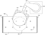
도 1은, 미립자 세정 조립체의 측면도이고;
[0013]
도 2는, 다른 구현예에 따른, 미립자 세정 조립체의 조감도(overhead view)이며; 그리고
[0014]
도 3은, 미립자 물질을 제거하는 방법의 블럭도이다.
[0015]
이해를 용이하게 하기 위하여, 가능하면, 도면들에 공통되는 동일한 엘리먼트들을 나타내기 위해, 동일한 참조번호들이 사용되었다. 일 실시예의 엘리먼트들 및 특징들이, 추가적인 언급 없이 다른 실시예들에 유익하게 통합될 수 있다는 점이 고려된다.[0011] In the manner in which the above-recited features can be understood in detail, a more particular description, briefly summarized above, may be had by reference to embodiments, some of which are illustrated in the accompanying drawings. It should be noted, however, that the appended drawings illustrate only typical embodiments and are not to be considered limiting of its scope, since the devices and methods described herein may allow other equally effective embodiments It is because.
[0012] Figure 1 is a side view of a particulate cleaning assembly;
[0013] FIG. 2 is an overhead view of a particulate cleaning assembly, according to another embodiment; And
[0014] FIG. 3 is a block diagram of a method for removing particulate matter.
In order to facilitate understanding, identical reference numerals have been used, where possible, to designate identical elements that are common to the figures. It is contemplated that the elements and features of one embodiment may be advantageously incorporated into other embodiments without further recitation.
[0016] 기판으로부터 후면 입자들을 제거하기 위한 디바이스들 및 방법들이 본원에서 개시된다. 후면 입자들은, 리소그래피 동안 디포커스(defocus) 및 오버레이 시프트(overlay shift)와 같이, 기판에 전달되는 방사선의 각도 및 강도에 영향을 줄 수 있다. 본원에서 설명되는 바와 같이, 기판의 후면 상에 존재하는 입자들은 접착 필름에 접착될 수 있다. 그런 다음에, 접착 필름은, 접착제 상의 입자 포화도(particle saturation)에 따라, 이후의 폐기 또는 재사용을 위해 기판으로부터 분리된다. 이러한 방식으로, 후면 입자들은 접착되어 기판으로부터 제거될 수 있다. 그런 다음에 기판은, 상기 설명된 문제들을 피하면서, 이후의 프로세싱을 겪을 수 있다.[0016] Devices and methods for removing backside particles from a substrate are disclosed herein. The backside particles can affect the angle and intensity of the radiation transmitted to the substrate, such as defocus and overlay shift during lithography. As described herein, particles present on the back surface of the substrate may be adhered to the adhesive film. The adhesive film is then separated from the substrate for subsequent disposal or reuse, depending on the particle saturation of the adhesive. In this manner, the backside particles can be bonded and removed from the substrate. The substrate may then undergo further processing while avoiding the problems described above.
[0017]
도 1은, 일 실시예에 따른 미립자 세정 조립체(100)의 측면도를 도시한다. 미립자 세정 조립체(100)는 챔버 본체(102)를 갖는 프로세스 챔버의 파트(part)일 수 있다. 미립자 세정 조립체(100)는, 플래튼(platen; 110)에 걸친 미립자 세정 물품(108)의 포지션과 관련하여 작용하는 예시적인 공급 조립체(104) 및 권취 조립체(106)를 더 포함한다. 일반적으로, 공급 조립체(104)는 상부 안내 부재(114) 및 하부 안내 부재(116)를 포함하고, 선택적으로 공급 롤(112)을 포함할 수 있다. 공급 롤(112)은 일반적으로, 미립자 세정 물품(108)의 사용되지 않은 부분을 포함한다. 공급 롤(112)은, 공급 롤(112) 상에 배치된 미립자 세정 물품(108)이 일단 미립자 세정 프로세스에 의해 소모되면, 새로운 미립자 세정 물품(108)을 포함하는 다른 공급 롤(112)로 쉽게 교체될 수 있도록 구성된다.[0017]
FIG. 1 illustrates a side view of a
[0018]
미립자 세정 물품(108)은 접착 재료를 포함한다. 접착 재료는 가요성이며, 기판으로부터 입자들이 제거될 수 있는 점착 강도(cohesive strength)을 갖는다. 일 구현예에서, 미립자 세정 물품(108)은 폴리이미드(polyimide) 층이다.[0018]
The
[0019]
하부 안내 부재(116)는 미립자 세정 물품(108)을 공급 롤(112)로부터 상부 안내 부재(114)로 인도(lead)하도록 포지셔닝된다. 상부 안내 부재(114)는, 상부 안내 부재(114)에서 시작되는(lead off) 미립자 세정 물품(108)이 실질적으로 동일 평면 상에 배치되도록, 즉, 플래튼(110)의 기판 지지 표면(118)에 바로 인접하여 평행하게 놓이도록 배치된다.[0019]
The
[0020]
일반적으로, 권취 조립체(106)는 상부 안내 부재(122) 및 하부 안내 부재(124)를 포함하고, 선택적으로 권취 롤(120)을 포함할 수 있다. 권취 롤(120)은 일반적으로, 미립자 세정 물품(108)의 사용된 부분을 포함하고, 일단 권취 롤(120)이, 사용된 미립자 세정 물품(108)으로 채워지면 빈 권취 롤로 쉽게 교체될 수 있도록 구성된다. 상부 안내 부재(122)는 미립자 세정 물품(108)을 플래튼(110)으로부터 하부 안내 부재(124)로 안내하도록 포지셔닝된다. 하부 안내 부재(124)는 미립자 세정 물품(108)을 권취 롤(120) 상으로 안내한다. 미립자 세정 조립체(100)는 또한, 기판 상에서 수행되는 입자 제거 프로세스에서 사용되는 바와 같은 미립자 세정 물품(108)에 대한 포화도의 상태 및 포지셔닝을 검출하기 위해 광 신호들을 송신하고 수신하도록 이루어진, 레이저 또는 카메라와 같은 광학 감지 디바이스(126)를 포함할 수 있다.[0020]
Generally, the
[0021]
미립자 세정 물품(108)은 일반적으로, 공급 조립체(104)에 커플링된 브레이크 또는 모터와 권취 조립체(106)에 커플링된 모터 사이에서 힘들을 밸런싱(balancing)함으로써 플래튼(110)에 대해 이동된다. 그런 다음, 광학 감지 디바이스(126)는, 미립자 세정 물품(108)의 포지션에 대해서, 플래튼(110)에 연결된 제어기(132)에 정보를 제공할 수 있다.[0021]
The
[0022]
플래튼(110)은, 함께 기판 척킹 디바이스(144)로 지칭되는 전극(142) 및 전력 공급부(128)를 더 포함할 수 있다. 전력 공급부(128)는 플래튼(110)에 배치된 전극(142)에 연결될 수 있다. 전극(142)에 전력이 인가되면, 전극(142)에 의해 기판 지지 표면(118)에 정전하(electrostatic charge)가 생성된다. 그런 다음에, 전극(142)에 의해 생성된 정전하는 기판(140)을 플래튼(110)의 기판 지지 표면(118)에 척킹할 수 있다. 플래튼(110)에 척킹될 때, 기판(140)의 후면은 미립자 세정 물품(108)에 대해 압박된다(urged).[0022]
The
[0023]
플래튼(110)은 복수의 리프트 핀들(130)을 더 포함할 수 있다. 리프트 핀들(130)은, 리프트 핀들이 미립자 세정 물품(108)의 개구부들을 관통하도록 포지셔닝될 수 있다. (도 2에 도시된 것과 같은)하나 또는 그 초과의 개구부들이 미립자 세정 물품(108)에 형성될 수 있다. 하나 또는 그 초과의 개구부들의 크기는 리프트 핀들(130)의 크기보다 더 크거나 그와 상응할 수 있다.[0023]
The
[0024]
제어기(132)는, 상기 설명된 바와 같이 미립자 세정 조립체(100)의 제어를 용이하게 하기 위해 미립자 세정 조립체(100)와 연결될 수 있다. 제어기(132)는 중앙 처리 장치(CPU)(134), 지원 회로들(138) 및 메모리(136)를 포함한다. CPU(134)는 다양한 드라이브들(drives), 로봇들 및 서브-프로세서들을 제어하기 위해 산업 현장(industrial setting)에서 사용될 수 있는 임의의 형태의 컴퓨터 프로세서 중 하나일 수 있다. 메모리(136)는 CPU(134)에 커플링된다. 메모리(136), 또는 컴퓨터-판독 가능한 매체는 용이하게 입수 가능한 메모리, 예컨대, 랜덤 액세스 메모리(RAM), 리드 온리 메모리(ROM), 플로피 디스크, 하드 디스크, 또는 로컬 또는 원격의 임의의 다른 형태의 디지털 저장소 중 하나 또는 그 초과일 수 있다. 지원 회로들(138)은 통상적인 방식으로 프로세서를 지원하기 위해 CPU(134)에 커플링된다. 이러한 회로들은 캐시, 전력 공급부들, 클록 회로들, 입력/출력 회로망 및 서브시스템들, 등을 포함한다.[0024]
The
[0025]
동작 시에, 후면 입자들을 포함하는 기판(140)은 플래튼 위의 미립자 세정 물품(108) 상에 포지셔닝된다. 기판(140)은 로봇 아암과 같은 다양한 장치 또는 기술들을 사용하여 포지셔닝될 수 있다. 그런 다음에, 기판(140)은 전력 공급부(128)에 의해 생성되는 정전하를 사용하여 플래튼(110)에 척킹된다. 미립자 세정 물품(108)은 접착제일 수 있다. 다른 예에서, 미립자 세정 물품(108)은 비-접착성 필름이다. 기판(140)의 후면 상에 존재하는 입자들은 미립자 세정 물품(108)에 접착되고 따라서 미립자 세정 물품(108)으로 전달된다. 입자들이 미립자 세정 물품(108)에 접착되는 시간을 허용한 후에, 플래튼(110)에서 전력 공급부(128)로부터 정전하를 생성하는 전력이 정지된다. 그런 다음, 기판(140)은 복수의 리프트 핀들(130)을 사용하여 미립자 세정 물품(108)으로부터 리프팅된다. 광학 감지 디바이스(126)는, 미립자 세정 물품(108)의 노출된 부분이 포화되었는지 아닌지를 결정하기 위해, 미립자 세정 물품(108)의 노출된 부분의 입자 밀도, 즉, 기판(140)을 수용한, 미립자 세정 물품(108)의 부분의 표면 면적 당 입자들의 양을 결정할 수 있다. 그런 다음에, 광학 감지 디바이스(126)는, 미립자 세정 물품(108)을 재포지셔닝(reposition)해야하는지 여부를 결정하기 위해 제어기(132)가 사용하는 신호들을 제공할 수 있다. 미립자 세정 물품(108)의 노출된 부분이 포화된 경우, 미립자 세정 물품(108)은, 포화된 부분이, 플래튼(110) 상에서 프로세싱되는 다음 기판(도시되지 않음)과 접촉하지 않도록 재포지셔닝된다. 예컨대, 권취 조립체(106)가 포화된 미립자 세정 물품(108)을 롤 투 롤 방식으로 수용하면서, 공급 조립체(104)는 미립자 세정 물품(108)의 사용되지 않은 부분을 플래튼(110) 위로 전진시킬 수 있다.[0025]
In operation, a
[0026]
다른 실시예에서, 미립자 세정 물품(108)은 추가적인 검출없이 변화된다. 여기서, 미립자 세정 물품(108)은, 접착된 입자 밀도에 대한 고려 없이, 특정 시간 기간 이후에 또는 특정 양의 기판 면적이 세정된 이후에, 예컨대, 매 기판(140) 이후에 전진된다.[0026]
In another embodiment, the
[0027]
도 2는, 다른 미립자 세정 조립체(200)의 측면도를 도시한다. 미립자 세정 조립체(200)는, 기판(140)을 미립자 세정 물품(108)에 고정시키기 위해 정전 척킹과 조합하여 또는 정전 척킹 대신에 로봇 아암(220)을 사용한다. 미립자 세정 조립체(200)는, 도 1에 대하여 설명된 바와 같이, 프로세싱 디바이스의 파트일 수 있다. 미립자 세정 조립체(200)는, 공급 조립체(104), 권취 조립체(106), 및 미립자 세정 물품(108)을 포함하여, 도 1에 대하여 설명된 하나 또는 그 초과의 컴포넌트들을 포함할 수 있다. 미립자 세정 물품(108)은, 도 1에 대해 도시된 플래튼(110) 위에 포지셔닝될 수 있다.[0027]
FIG. 2 shows a side view of another
[0028]
복수의 개구부들(202)은 미립자 세정 물품(108)에 형성될 수 있다. 개구부들(202)은, 리프트 핀들(130)이 미립자 세정 물품(108)을 리프팅하지 않고 통과할 수 있도록 적절한 직경 및 위치로 이루어질 수 있다. 개구부들은, 도 1에 대해 설명된 광학 감지 디바이스(126)를 사용하여 리프트 핀들(130) 위에 포지셔닝된다. 개구부들(202)은 임의의 형상, 예컨대, 원형, 타원형, 직사각형, 또는 다른 더 복잡한 형상들로 이루어질 수 있다. 또한, 본원에 도시된 것보다 더 많은 또는 더 적은 개구부들(202)이 존재할 수 있다. 개구부들(202)은 균일하게 포지셔닝될 필요는 없다.[0028]
A plurality of
[0029]
로봇 아암(220)은 베이스(222), 연장 부분(224) 및 기판 캐리어(226)를 포함한다. 로봇 아암(220)은 스테인리스 스틸, 알루미늄, 또는 다른 것들과 같은 다양한 재료들 중 하나 또는 그 초과로 구성될 수 있다. 연장 부분(224)은 기판 캐리어(226)의 제어된 운동을 제공할 수 있다. 연장 부분(224)은 6자유도로 움직일 수 있다. 다른 실시예에서, 하나 또는 그 초과의 자유도는 동작 동안 고정된다(locked). 기판 캐리어(226)는 기판(140)과 최소한으로 접촉하면서 기판(140)을 운반한다.[0029]
The
[0030]
동작 시에, 로봇 아암(220)은 기판 캐리어(226)를 사용하여 기판(140)을 수용한다. 기판(140)은 복수의 후면 입자들을 가질 수 있다. 기판 캐리어(226)는, 제어기(132)에 의해 제어되는 바와 같이, 베이스(222) 및 연장 부분(224) 양자 모두의 적절하게 제어되는 움직임에 의해 미립자 세정 물품(108) 위에 정확하게 포지셔닝된다. 그런 다음에, 로봇 아암(220)은 기판(140)의 후면을 미립자 세정 물품(108)과 접촉하도록 포지셔닝한다. 로봇 아암(220)은 제 위치(in place)에 남아 있을 수 있거나, 기판(140)으로부터 분리될 수 있다. 어느 경우에든, 도 1에 대하여 설명된 바와 같이, 기판(140)은 포지션(204)에서 플래튼(110)에 정전기적으로 척킹될 수 있다. 기판(140)의 후면 상에 존재하는 입자들이 미립자 세정 물품(108)에 접착되도록 허용하는 적절한 양의 시간 이후에, 기판(140)은 리프트 핀들(130)을 사용하거나 로봇 아암(220)을 사용하여 미립자 세정 물품(108)으로부터 리프팅된다. 그런 다음에, 미립자 세정 물품(108)은, 상기 설명된 바와 같이, 시간, 입자 밀도, 세정된 기판들의 개수, 또는 이들의 조합들에 기초하여 전진된다. 그런 다음에, 광학 감지 디바이스(126)는, 미립자 세정 물품(108)의 포지션을 결정하기 위해 제어기(132)가 사용하는 신호들을 제공할 수 있다. 그런 다음에, 미립자 세정 물품(108)은 제 2 기판(도시되지 않음)과의 접촉을 위해 플래튼(110) 위에 재포지셔닝될 수 있다.[0030]
In operation,
[0031]
도 3은, 기판으로부터 입자들을 제거하는 방법의 블록도이다. 방법(300)은, 블록(302)에서, 기판을 프로세스 챔버에 포지셔닝하는 단계를 포함하고, 기판은 후면 표면을 가지며, 후면 표면은 후면 표면 상에 형성된 복수의 입자들을 갖는다. 블록(304)에서, 기판의 적어도 부분을 기판 척킹 디바이스에 척킹한다. 기판 척킹 디바이스는, 미립자 세정 물품이 기판 후면 표면 상에 포지셔닝된 기판 후면 표면을 갖는다. 블록(306)에서, 기판이 미립자 세정 물품으로부터 분리되고, 기판의 후면 표면 상에 존재하는 복수의 입자들 중 적어도 부분은 미립자 세정 물품에 접착되어 미립자 세정 물품으로 전달된다. 접착성 필름을 포함하는 프로세스 챔버를 채용함으로써, 1μm 또는 그 미만의 평균 직경을 갖는 입자들은 기판의 후면 표면으로부터 효과적으로 제거될 수 있다.[0031]
Figure 3 is a block diagram of a method for removing particles from a substrate. The
[0032]
방법(300)은, 블록(302)에서, 기판을 프로세스 챔버에 포지셔닝하는 단계에 의해 시작되며, 기판은 후면 표면을 가지고, 후면 표면은 후면 표면 상에 형성된 복수의 입자들을 갖는다. 방법(300)은, 실리콘, 에폭시, 또는 석영 기판과 같이, 반도체 애플리케이션들에 사용 가능한 임의의 조성을 갖는 기판들에 사용될 수 있다. 일 실시예에서, 기판은 실질적으로 유리로 구성된다. 기판은 광범위한 치수들(예컨대, 길이, 폭, 형상, 두께, 등)로 이루어질 수 있다. 일 예에서, 기판은 대략 1미터 길이 및 1미터 폭이다. 방법(300)은 도 1 및 2에 대해 설명된 프로세스 챔버와 같은 프로세스 챔버에서 수행될 수 있다.[0032]
The
[0033]
블록(304)에서, 기판이 챔버 내에 있는 상태에서, 기판의 적어도 부분은 기판 척킹 디바이스에 척킹되고 따라서 미립자 세정 물품에 대해 유지된다. 기판은 로봇 아암 또는 클램프들과 같은 기계적인 디바이스들을 사용하여 기판 척킹 디바이스 근처에서 유지될 수 있거나, 정전하를 사용하여 유지될 수 있다. 기판 척킹 디바이스는, 미립자 세정 물품이 기판 후면 표면 상에 포지셔닝된 기판 후면 표면을 갖는다. 미립자 세정 물품은 도 1 및 2에 대해 설명된 바와 같은 미립자 세정 물품일 수 있다.[0033]
At
[0034]
그런 다음에, 블록(306)에서, 기판이 미립자 세정 물품으로부터 분리되고, 기판의 후면 상에 존재하는 복수의 입자들 중 적어도 부분은 미립자 세정 물품의 접착제에 접착되어 미립자 세정 물품의 접착제로 전달된다. 예컨대, 리프트 핀들에 의해, 로봇 아암을 사용하여, 또는 이들의 조합들에 의해, 기판은 미립자 세정 물품으로부터 분리된다. 일단 분리되면, 기판은 추가적인 프로세싱을 위해 이송된다.[0034]
Then, at
[0035]
블록(308)에서, 기판이 기판 세정 물품으로부터 분리되고, 그런 다음에 미립자 세정 물품이 인덱싱된다. 본원에서 사용되는 바와 같은 인덱싱은, 하나 또는 그 초과의 개구부들 및 기판 척킹 디바이스에 대한 미립자 세정 물품의 제 1 또는 현재 포지션을 결정하는 것을 포함한다. 그런 다음에 제 1 포지션은 제어기로 중계된다(relayed). 그런 다음에, 제어기는 중계된 포지션에 기초하여 미립자 세정 물품을 조정한다. 미립자 세정 물품의 포지션은, 미립자 세정 물품의 부분이, 기판 척킹 디바이스의 대응하는 부분 위에 적절하게 포지셔닝되도록 제 2 포지션으로 조정된다. 예컨대, 도 2에 대해 설명된, 미립자 세정 물품의 개구부들은, 기판 척킹 디바이스의 리프트 핀들 위에 포지셔닝될 수 있다.[0035]
At
[0036] 일단 입자들이 기판의 후면 표면으로부터 제거되면, 기판은 추가적인 프로세싱을 위해 이송될 수 있다. 일 예에서, 기판은 리소그래피 프로세스를 위해 제 2 프로세스 챔버로 이송된다.[0036] Once the particles are removed from the back surface of the substrate, the substrate can be transferred for further processing. In one example, the substrate is transferred to a second process chamber for a lithographic process.
[0037] 본원에서 설명되는 방법은 후면 미립자가 프로세싱 이전에 제거되는 것을 허용한다. 교환 가능한 미립자 세정 물품은 세정 품질의 손실 없이 높은 처리량을 허용한다. 상기 설명된 바와 같이, 후면 입자들은 다양한 유형의 디바이스 불량, 예컨대, 인터커넥트 구조들에서의 전기 접촉 불량들 및 교차 오염뿐만 아니라, 리소그래피 프로세스들에서의 임계 치수에 대한 제어의 부재로 기인한 기판 뒤틀림으로 이어질 수 있다. 추가적인 프로세싱 이전에 미립자가 있는 기판의 후면을 세정함으로써, 이러한 디바이스 불량의 원인들이 회피될 수 있다.[0037] The method described herein allows the backside particulates to be removed prior to processing. Exchangeable particulate cleaning articles allow high throughput without loss of cleaning quality. As described above, the backside particles are subject to various types of device defects, such as electrical contact failures and cross contamination in interconnect structures, as well as substrate distortion due to lack of control over critical dimensions in lithographic processes . By cleaning the backside of the substrate with particulates prior to further processing, the causes of such device defects can be avoided.
[0038] 전술한 내용은 본원에서 설명된 디바이스들 및 방법들의 실시예들에 관한 것이지만, 그의 기본적인 범위로부터 벗어나지 않고 다른 그리고 추가적인 실시예들이 안출될 수 있으며, 그의 범위는 이하의 청구항들에 의해서 결정된다.[0038] While the foregoing is directed to embodiments of the devices and methods described herein, other and further embodiments may be devised without departing from the basic scope thereof, and the scope thereof is determined by the claims that follow.
Claims (15)
기판 지지 표면을 갖는 기판 척킹(chucking) 디바이스;
미립자 세정 물품을 수용하도록 구성된 공급 조립체 및 권취(take up) 조립체 - 상기 기판 지지 표면 위에 있고 그리고 상기 기판 지지 표면과 접촉하는 상기 미립자 세정 물품에 대한 경로를 가짐 -; 및
상기 미립자 세정 물품과 기판을 분리하도록 구성된 기판 포지셔닝 디바이스를 포함하는,
입자들을 제거하기 위한 디바이스.A device for removing particles,
A substrate chucking device having a substrate support surface;
A feed assembly and a take up assembly configured to receive a particulate cleaning article having a path to the particulate cleaning article on the substrate support surface and in contact with the substrate support surface; And
A substrate positioning device configured to separate the substrate from the particulate cleaning article,
A device for removing particles.
상기 기판 포지셔닝 디바이스는 복수의 리프트 핀들을 포함하는,
입자들을 제거하기 위한 디바이스.The method according to claim 1,
Wherein the substrate positioning device comprises a plurality of lift pins,
A device for removing particles.
상기 미립자 세정 물품은, 상기 미립자 세정 물품에 형성되고 상기 복수의 리프트 핀들과 정렬되도록 구성된 복수의 개구부들을 갖는,
입자들을 제거하기 위한 디바이스.3. The method of claim 2,
Wherein the particulate cleaning article has a plurality of openings formed in the particulate cleaning article and configured to be aligned with the plurality of lift pins,
A device for removing particles.
상기 기판 척킹 디바이스는 정전기력을 제공하도록 구성된 전극을 포함하는,
입자들을 제거하기 위한 디바이스.The method according to claim 1,
Wherein the substrate chucking device comprises an electrode configured to provide an electrostatic force.
A device for removing particles.
상기 미립자 세정 물품은 웨브(web)인,
입자들을 제거하기 위한 디바이스.The method according to claim 1,
The particulate cleaning article is a web,
A device for removing particles.
상기 미립자 세정 물품은 상기 기판 지지 표면에 대해 비-접착성인,
입자들을 제거하기 위한 디바이스.The method according to claim 1,
Wherein the particulate cleaning article is non-adhesive to the substrate support surface,
A device for removing particles.
상기 기판 포지셔닝 디바이스는 상기 미립자 세정 물품의 포화도(saturation) 및 포지션 양자 모두를 결정하는,
입자들을 제거하기 위한 디바이스.The method according to claim 1,
Wherein the substrate positioning device determines both a saturation and a position of the particulate cleaning article,
A device for removing particles.
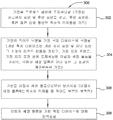
기판의 후면의 적어도 부분을 기판 척킹 디바이스에 척킹하는 단계 - 상기 기판 척킹 디바이스는 기판 지지 표면 및 하나 또는 그 초과의 리프트 핀들을 갖고, 상기 기판 지지 표면은 상기 기판 지지 표면 상에 포지셔닝된 미립자 세정 물품을 가지며, 상기 미립자 세정 물품은 하나 또는 그 초과의 개구부들을 가짐 -;
상기 기판을 상기 미립자 세정 물품으로부터 분리하는 단계 - 복수의 입자들 중 적어도 부분은 상기 미립자 세정 물품에 접착되어 상기 미립자 세정 물품으로 전달됨 -; 및
상기 하나 또는 그 초과의 개구부들이 상기 하나 또는 그 초과의 리프트 핀들 위에 포지셔닝되도록 상기 미립자 세정 물품을 인덱싱하는(indexing) 단계를 포함하는,
입자들을 제거하기 위한 방법.A method for removing particles,
Chucking at least a portion of a backside of a substrate with a substrate chucking device, the substrate chucking device having a substrate support surface and one or more lift pins, wherein the substrate support surface is positioned on the substrate support surface, The particulate cleaning article having one or more openings;
Separating the substrate from the particulate cleaning article, at least a portion of the plurality of particles being adhered to the particulate cleaning article and transferred to the particulate cleaning article; And
Indexing the particulate cleaning article such that the one or more openings are positioned over the one or more lift pins.
A method for removing particles.
상기 기판 척킹 디바이스에 걸쳐 상기 미립자 세정 물품을 전진시키는 단계를 더 포함하는,
입자들을 제거하기 위한 방법.9. The method of claim 8,
Further comprising advancing the particulate cleaning article across the substrate chucking device,
A method for removing particles.
척킹하는 단계는, 상기 기판 지지 표면 상에 정전기력을 생성하는 것, 또는 로봇 아암을 사용하여 상기 미립자 세정 물품에 대해 상기 기판을 포지셔닝하는 것을 더 포함하는,
입자들을 제거하기 위한 방법.9. The method of claim 8,
The chucking step further comprises generating an electrostatic force on the substrate support surface, or positioning the substrate with respect to the particulate cleaning article using a robotic arm.
A method for removing particles.
상기 미립자 세정 물품은 폴리이미드(polyimide)를 포함하는,
입자들을 제거하기 위한 방법.9. The method of claim 8,
Wherein the particulate cleaning article comprises a polyimide,
A method for removing particles.
기판 지지 표면 및 복수의 리프트 핀들을 갖는 기판 척킹 디바이스;
상기 기판 지지 표면 위에 포지셔닝된 전진 가능한 미립자 세정 물품 - 상기 미립자 세정 물품은 상기 미립자 세정 물품에 형성된 복수의 리프트 핀 개구부들을 가짐 -; 및
상기 미립자 세정 물품을 상기 기판 척킹 디바이스 상에 포지셔닝하기 위한 메트릭(metric)을 제공하도록 구성된 광학 감지 디바이스를 포함하는,
입자들을 제거하기 위한 디바이스.A device for removing particles,
A substrate chucking device having a substrate support surface and a plurality of lift pins;
A forward particulate cleaning article positioned on the substrate support surface, the particulate cleaning article having a plurality of lift pin openings formed in the particulate cleaning article; And
And an optical sensing device configured to provide a metric for positioning the particulate cleaning article on the substrate chucking device.
A device for removing particles.
상기 광학 감지 디바이스는 상기 미립자 세정 물품의 포화도 및 포지션 양자 모두를 결정하는,
입자들을 제거하기 위한 디바이스.13. The method of claim 12,
Wherein the optical sensing device determines both the degree of saturation and the position of the particulate cleaning article,
A device for removing particles.
상기 기판 척킹 디바이스는 정전기력을 제공하도록 구성된 전극을 포함하는,
입자들을 제거하기 위한 디바이스.13. The method of claim 12,
Wherein the substrate chucking device comprises an electrode configured to provide an electrostatic force.
A device for removing particles.
상기 미립자 세정 물품은, 상기 미립자 세정 물품의, 등지는(facing away) 측 상에 배치된 접착층을 포함하는,
입자들을 제거하기 위한 디바이스.13. The method of claim 12,
Wherein the particulate cleaning article comprises an adhesive layer disposed on the back away side of the particulate cleaning article,
A device for removing particles.
Applications Claiming Priority (5)
| Application Number | Priority Date | Filing Date | Title |
|---|---|---|---|
| US201462014278P | 2014-06-19 | 2014-06-19 | |
| US62/014,278 | 2014-06-19 | ||
| US14/476,398 | 2014-09-03 | ||
| US14/476,398 US9815091B2 (en) | 2014-06-19 | 2014-09-03 | Roll to roll wafer backside particle and contamination removal |
| PCT/US2015/033005 WO2015195292A1 (en) | 2014-06-19 | 2015-05-28 | Roll to roll wafer backside particle and contamination removal |
Publications (1)
| Publication Number | Publication Date |
|---|---|
| KR20170018069A true KR20170018069A (en) | 2017-02-15 |
Family
ID=54870310
Family Applications (1)
| Application Number | Title | Priority Date | Filing Date |
|---|---|---|---|
| KR1020177001599A KR20170018069A (en) | 2014-06-19 | 2015-05-28 | Roll to roll wafer backside particle and contamination removal |
Country Status (6)
| Country | Link |
|---|---|
| US (1) | US9815091B2 (en) |
| JP (1) | JP6573918B2 (en) |
| KR (1) | KR20170018069A (en) |
| CN (1) | CN106463385B (en) |
| TW (1) | TWI663629B (en) |
| WO (1) | WO2015195292A1 (en) |
Families Citing this family (4)
| Publication number | Priority date | Publication date | Assignee | Title |
|---|---|---|---|---|
| KR102640172B1 (en) | 2019-07-03 | 2024-02-23 | 삼성전자주식회사 | Processing apparatus for a substrate and method of driving the same |
| CN111250481B (en) * | 2020-01-17 | 2021-07-13 | 哈尔滨工业大学 | Device for adsorbing particle pollutants by utilizing movable electrostatic electric field |
| US20230173557A1 (en) * | 2020-03-17 | 2023-06-08 | Tokyo Electron Limited | Cleaning method and method of manufacturing semiconductor device |
| US20220359234A1 (en) * | 2021-05-07 | 2022-11-10 | Kla Corporation | Electrostatic substrate cleaning system and method |
Family Cites Families (23)
| Publication number | Priority date | Publication date | Assignee | Title |
|---|---|---|---|---|
| JPH06232108A (en) * | 1993-01-29 | 1994-08-19 | Hitachi Ltd | Removal of foreign matter |
| US5456758A (en) | 1993-04-26 | 1995-10-10 | Sematech, Inc. | Submicron particle removal using liquid nitrogen |
| US5972051A (en) | 1993-06-17 | 1999-10-26 | Vlsi Technology, Inc | Method and apparatus for removing particles from semiconductor wafer edges using a particle withdrawing means |
| JPH07275805A (en) * | 1994-04-05 | 1995-10-24 | Nitto Seiki Kk | Surface-cleaning device for sheet-shaped body |
| JPH08148461A (en) * | 1994-11-18 | 1996-06-07 | Nitto Denko Corp | Method for removing foreign object attached to semiconductor wafer |
| US5891298A (en) * | 1995-08-31 | 1999-04-06 | Nitto Denko Corporation | Method and apparatus for peeling protective adhesive tape from semiconductor wafer |
| JPH1098090A (en) * | 1996-09-25 | 1998-04-14 | Canon Inc | Substrate holding device and exposure system |
| JP3809503B2 (en) * | 1997-02-28 | 2006-08-16 | 野村マイクロ・サイエンス株式会社 | Method and apparatus for cleaning the inside of a semiconductor substrate |
| US5753563A (en) | 1997-07-30 | 1998-05-19 | Chartered Semiconductor Manufacturing Ltd. | Method of removing particles by adhesive |
| JP3616725B2 (en) | 1998-12-07 | 2005-02-02 | 信越半導体株式会社 | Substrate processing method and processing apparatus |
| US6244944B1 (en) | 1999-08-31 | 2001-06-12 | Micron Technology, Inc. | Method and apparatus for supporting and cleaning a polishing pad for chemical-mechanical planarization of microelectronic substrates |
| US6523208B1 (en) | 2000-03-24 | 2003-02-25 | Xerox Corporation | Flexible web cleaning system |
| JP2002083795A (en) * | 2000-09-07 | 2002-03-22 | Toshiba Corp | Method and device for washing semiconductor wafer |
| JP4414116B2 (en) * | 2001-08-21 | 2010-02-10 | 芝浦メカトロニクス株式会社 | Substrate cleaning apparatus and substrate cleaning method |
| US6695917B2 (en) * | 2001-11-14 | 2004-02-24 | Nordson Corporation | Flow through felt dispenser |
| US6884152B2 (en) | 2003-02-11 | 2005-04-26 | Micron Technology, Inc. | Apparatuses and methods for conditioning polishing pads used in polishing micro-device workpieces |
| US20050210610A1 (en) * | 2004-03-26 | 2005-09-29 | Zih Corp. | Apparatus and methods for cleaning the components of a feed device |
| TWI420579B (en) * | 2005-07-12 | 2013-12-21 | Creative Tech Corp | And a foreign matter removing method for a substrate |
| US7264539B2 (en) | 2005-07-13 | 2007-09-04 | Micron Technology, Inc. | Systems and methods for removing microfeature workpiece surface defects |
| JP4607748B2 (en) * | 2005-12-02 | 2011-01-05 | 東京エレクトロン株式会社 | Substrate particle removal method, apparatus and coating and developing apparatus |
| US7784146B2 (en) * | 2006-01-09 | 2010-08-31 | International Business Machines Corporation | Probe tip cleaning apparatus and method of use |
| JP2011093113A (en) * | 2009-10-27 | 2011-05-12 | Fujifilm Corp | Device and method for manufacturing laminated substrate |
| JP6014477B2 (en) * | 2012-12-04 | 2016-10-25 | 東京エレクトロン株式会社 | Peeling device, peeling system and peeling method |
-
2014
- 2014-09-03 US US14/476,398 patent/US9815091B2/en not_active Expired - Fee Related
-
2015
- 2015-05-28 WO PCT/US2015/033005 patent/WO2015195292A1/en active Application Filing
- 2015-05-28 CN CN201580032653.0A patent/CN106463385B/en not_active Expired - Fee Related
- 2015-05-28 JP JP2016573865A patent/JP6573918B2/en not_active Expired - Fee Related
- 2015-05-28 KR KR1020177001599A patent/KR20170018069A/en not_active Application Discontinuation
- 2015-06-04 TW TW104118139A patent/TWI663629B/en not_active IP Right Cessation
Also Published As
| Publication number | Publication date |
|---|---|
| US9815091B2 (en) | 2017-11-14 |
| US20150371879A1 (en) | 2015-12-24 |
| TWI663629B (en) | 2019-06-21 |
| CN106463385B (en) | 2020-07-14 |
| WO2015195292A1 (en) | 2015-12-23 |
| TW201604930A (en) | 2016-02-01 |
| CN106463385A (en) | 2017-02-22 |
| JP6573918B2 (en) | 2019-09-11 |
| JP2017522726A (en) | 2017-08-10 |
Similar Documents
| Publication | Publication Date | Title |
|---|---|---|
| TWI550755B (en) | Processing apparatus and device manufacturing method | |
| KR20170018069A (en) | Roll to roll wafer backside particle and contamination removal | |
| JP4519199B2 (en) | Wafer recycling method and wafer recycling apparatus | |
| TW201946140A (en) | Substrate processing system and substrate processing method | |
| TW201331721A (en) | Cleaning a support that holds a patterning device inside a lithography apparatus | |
| JP7261000B2 (en) | CONTAINER, PROCESSING APPARATUS, CONTENT REMOVAL METHOD, AND PRODUCT MANUFACTURING METHOD | |
| JP7365827B2 (en) | Joining system and joining method | |
| JP6568773B2 (en) | Substrate transfer device and peeling system | |
| TWI812622B (en) | Gettering layer forming device, gettering layer forming method, and computer storage medium | |
| KR20070074398A (en) | Semiconductor wafer including contamination removal part | |
| US10262853B2 (en) | Removing particulate contaminants from the backside of a wafer or reticle | |
| US9721783B2 (en) | Methods for particle reduction in semiconductor processing | |
| JPH0547906A (en) | Plane object holding means and equipment using the same | |
| JP2017071202A (en) | Fine pattern transfer method to surface uneven article to be treated using film for uneven surface sticking | |
| US11626302B2 (en) | Bonding method for cleaning non-bonding surface of substrate | |
| TW201918441A (en) | Substrate processing method | |
| JP5518587B2 (en) | Cutting tool manufacturing method | |
| CN108398857B (en) | Lithographic apparatus and method of manufacturing article | |
| US9829806B2 (en) | Lithography tool with backside polisher | |
| KR20180124732A (en) | Imprint method, imprint apparatus, imprint system, and method of manufacturing article | |
| JPH0757980A (en) | Using method of semiconductor wafer and manufacture of semiconductor device | |
| KR20070115331A (en) | Exposure system | |
| KR20000011777U (en) | Wafer Chuck of Exposure Equipment |
Legal Events
| Date | Code | Title | Description |
|---|---|---|---|
| A201 | Request for examination | ||
| E902 | Notification of reason for refusal | ||
| E601 | Decision to refuse application |