KR20160100363A - 오직 수신기 클록에 의한 CCIe 수신기 로직 레지스터 기입 - Google Patents
오직 수신기 클록에 의한 CCIe 수신기 로직 레지스터 기입 Download PDFInfo
- Publication number
- KR20160100363A KR20160100363A KR1020167019339A KR20167019339A KR20160100363A KR 20160100363 A KR20160100363 A KR 20160100363A KR 1020167019339 A KR1020167019339 A KR 1020167019339A KR 20167019339 A KR20167019339 A KR 20167019339A KR 20160100363 A KR20160100363 A KR 20160100363A
- Authority
- KR
- South Korea
- Prior art keywords
- transitions
- symbols
- registers
- data bits
- clock
- Prior art date
- Legal status (The legal status is an assumption and is not a legal conclusion. Google has not performed a legal analysis and makes no representation as to the accuracy of the status listed.)
- Withdrawn
Links
Images


Classifications
-
- G—PHYSICS
- G06—COMPUTING OR CALCULATING; COUNTING
- G06F—ELECTRIC DIGITAL DATA PROCESSING
- G06F13/00—Interconnection of, or transfer of information or other signals between, memories, input/output devices or central processing units
- G06F13/38—Information transfer, e.g. on bus
- G06F13/42—Bus transfer protocol, e.g. handshake; Synchronisation
- G06F13/4204—Bus transfer protocol, e.g. handshake; Synchronisation on a parallel bus
- G06F13/4221—Bus transfer protocol, e.g. handshake; Synchronisation on a parallel bus being an input/output bus, e.g. ISA bus, EISA bus, PCI bus, SCSI bus
-
- G—PHYSICS
- G06—COMPUTING OR CALCULATING; COUNTING
- G06F—ELECTRIC DIGITAL DATA PROCESSING
- G06F1/00—Details not covered by groups G06F3/00 - G06F13/00 and G06F21/00
- G06F1/04—Generating or distributing clock signals or signals derived directly therefrom
-
- G—PHYSICS
- G06—COMPUTING OR CALCULATING; COUNTING
- G06F—ELECTRIC DIGITAL DATA PROCESSING
- G06F13/00—Interconnection of, or transfer of information or other signals between, memories, input/output devices or central processing units
- G06F13/38—Information transfer, e.g. on bus
- G06F13/42—Bus transfer protocol, e.g. handshake; Synchronisation
- G06F13/4282—Bus transfer protocol, e.g. handshake; Synchronisation on a serial bus, e.g. I2C bus, SPI bus
- G06F13/4291—Bus transfer protocol, e.g. handshake; Synchronisation on a serial bus, e.g. I2C bus, SPI bus using a clocked protocol
-
- G—PHYSICS
- G06—COMPUTING OR CALCULATING; COUNTING
- G06F—ELECTRIC DIGITAL DATA PROCESSING
- G06F13/00—Interconnection of, or transfer of information or other signals between, memories, input/output devices or central processing units
- G06F13/38—Information transfer, e.g. on bus
- G06F13/42—Bus transfer protocol, e.g. handshake; Synchronisation
- G06F13/4282—Bus transfer protocol, e.g. handshake; Synchronisation on a serial bus, e.g. I2C bus, SPI bus
- G06F13/4295—Bus transfer protocol, e.g. handshake; Synchronisation on a serial bus, e.g. I2C bus, SPI bus using an embedded synchronisation
-
- G—PHYSICS
- G06—COMPUTING OR CALCULATING; COUNTING
- G06F—ELECTRIC DIGITAL DATA PROCESSING
- G06F1/00—Details not covered by groups G06F3/00 - G06F13/00 and G06F21/00
- G06F1/26—Power supply means, e.g. regulation thereof
- G06F1/32—Means for saving power
- G06F1/3203—Power management, i.e. event-based initiation of a power-saving mode
- G06F1/3234—Power saving characterised by the action undertaken
- G06F1/3237—Power saving characterised by the action undertaken by disabling clock generation or distribution
-
- G—PHYSICS
- G06—COMPUTING OR CALCULATING; COUNTING
- G06F—ELECTRIC DIGITAL DATA PROCESSING
- G06F1/00—Details not covered by groups G06F3/00 - G06F13/00 and G06F21/00
- G06F1/26—Power supply means, e.g. regulation thereof
- G06F1/32—Means for saving power
- G06F1/3203—Power management, i.e. event-based initiation of a power-saving mode
- G06F1/3234—Power saving characterised by the action undertaken
- G06F1/324—Power saving characterised by the action undertaken by lowering clock frequency
-
- G—PHYSICS
- G06—COMPUTING OR CALCULATING; COUNTING
- G06F—ELECTRIC DIGITAL DATA PROCESSING
- G06F13/00—Interconnection of, or transfer of information or other signals between, memories, input/output devices or central processing units
-
- H—ELECTRICITY
- H04—ELECTRIC COMMUNICATION TECHNIQUE
- H04L—TRANSMISSION OF DIGITAL INFORMATION, e.g. TELEGRAPHIC COMMUNICATION
- H04L7/00—Arrangements for synchronising receiver with transmitter
- H04L7/0079—Receiver details
- H04L7/0087—Preprocessing of received signal for synchronisation, e.g. by code conversion, pulse generation or edge detection
-
- H—ELECTRICITY
- H04—ELECTRIC COMMUNICATION TECHNIQUE
- H04L—TRANSMISSION OF DIGITAL INFORMATION, e.g. TELEGRAPHIC COMMUNICATION
- H04L7/00—Arrangements for synchronising receiver with transmitter
- H04L7/02—Speed or phase control by the received code signals, the signals containing no special synchronisation information
- H04L7/027—Speed or phase control by the received code signals, the signals containing no special synchronisation information extracting the synchronising or clock signal from the received signal spectrum, e.g. by using a resonant or bandpass circuit
Landscapes
- Engineering & Computer Science (AREA)
- Theoretical Computer Science (AREA)
- Physics & Mathematics (AREA)
- General Engineering & Computer Science (AREA)
- General Physics & Mathematics (AREA)
- Information Transfer Systems (AREA)
Applications Claiming Priority (5)
| Application Number | Priority Date | Filing Date | Title |
|---|---|---|---|
| US201361917895P | 2013-12-18 | 2013-12-18 | |
| US61/917,895 | 2013-12-18 | ||
| US14/572,680 US10031547B2 (en) | 2013-12-18 | 2014-12-16 | CCIe receiver logic register write only with receiver clock |
| US14/572,680 | 2014-12-16 | ||
| PCT/US2014/070935 WO2015095382A1 (en) | 2013-12-18 | 2014-12-17 | CCIe RECEIVER LOGIC REGISTER WRITE ONLY WITH RECEIVER CLOCK |
Publications (1)
| Publication Number | Publication Date |
|---|---|
| KR20160100363A true KR20160100363A (ko) | 2016-08-23 |
Family
ID=53368356
Family Applications (1)
| Application Number | Title | Priority Date | Filing Date |
|---|---|---|---|
| KR1020167019339A Withdrawn KR20160100363A (ko) | 2013-12-18 | 2014-12-17 | 오직 수신기 클록에 의한 CCIe 수신기 로직 레지스터 기입 |
Country Status (7)
| Country | Link |
|---|---|
| US (1) | US10031547B2 (enExample) |
| EP (1) | EP3084619A1 (enExample) |
| JP (1) | JP2017501493A (enExample) |
| KR (1) | KR20160100363A (enExample) |
| CN (1) | CN105830045A (enExample) |
| BR (1) | BR112016014347A2 (enExample) |
| WO (1) | WO2015095382A1 (enExample) |
Families Citing this family (3)
| Publication number | Priority date | Publication date | Assignee | Title |
|---|---|---|---|---|
| CN111934707B (zh) | 2019-04-25 | 2024-07-09 | 恩智浦有限公司 | 数据发射代码和接口 |
| US12278636B2 (en) * | 2022-11-28 | 2025-04-15 | Parade Technologies, Ltd. | Receiver circuit with automatic DC offset cancellation in display port applications |
| US12306693B2 (en) * | 2023-05-12 | 2025-05-20 | Mediatek Inc. | Method and device for saving power |
Family Cites Families (17)
| Publication number | Priority date | Publication date | Assignee | Title |
|---|---|---|---|---|
| DE2440768C3 (de) | 1974-08-26 | 1982-03-18 | Philips Patentverwaltung Gmbh, 2000 Hamburg | Verfahren und Vorrichtung zur Datenkompression für die Faksimile-Übertragung graphischer Information |
| GB2120054B (en) | 1982-04-23 | 1985-07-31 | Gen Electric Co Plc | Digital data signalling systems |
| US5640605A (en) * | 1994-08-26 | 1997-06-17 | 3Com Corporation | Method and apparatus for synchronized transmission of data between a network adaptor and multiple transmission channels using a shared clocking frequency and multilevel data encoding |
| US5850422A (en) | 1995-07-21 | 1998-12-15 | Symbios, Inc. | Apparatus and method for recovering a clock signal which is embedded in an incoming data stream |
| JP2002351825A (ja) * | 2001-05-29 | 2002-12-06 | Rohm Co Ltd | 通信システム |
| US7007120B2 (en) | 2003-04-25 | 2006-02-28 | Hewlett-Packard Development Company, L.P. | Information transfer protocol having sync fields of different lengths |
| US7289528B2 (en) | 2003-08-29 | 2007-10-30 | Motorola, Inc. | Component interconnect with self-clocking data |
| US7631118B2 (en) | 2003-12-31 | 2009-12-08 | Intel Corporation | Lane to lane deskewing via non-data symbol processing for a serial point to point link |
| US7444558B2 (en) | 2003-12-31 | 2008-10-28 | Intel Corporation | Programmable measurement mode for a serial point to point link |
| US7386661B2 (en) | 2004-10-13 | 2008-06-10 | Marvell International Ltd. | Power save module for storage controllers |
| US7916820B2 (en) * | 2006-12-11 | 2011-03-29 | International Business Machines Corporation | Systems and arrangements for clock and data recovery in communications |
| KR100898305B1 (ko) | 2007-10-08 | 2009-05-19 | 주식회사 티엘아이 | 3라인 차동 신호법을 위한 클락 임베디드 차동 데이터수신장치 |
| JP2010250048A (ja) * | 2009-04-15 | 2010-11-04 | Panasonic Corp | 送信装置、受信装置、データ伝送システム、及び画像表示装置 |
| US9118457B2 (en) * | 2013-03-15 | 2015-08-25 | Qualcomm Incorporated | Multi-wire single-ended push-pull link with data symbol transition based clocking |
| US20150100711A1 (en) * | 2013-10-07 | 2015-04-09 | Qualcomm Incorporated | Low power camera control interface bus and devices |
| US9426082B2 (en) * | 2014-01-03 | 2016-08-23 | Qualcomm Incorporated | Low-voltage differential signaling or 2-wire differential link with symbol transition clocking |
| US20150220472A1 (en) * | 2014-02-05 | 2015-08-06 | Qualcomm Incorporated | Increasing throughput on multi-wire and multi-lane interfaces |
-
2014
- 2014-12-16 US US14/572,680 patent/US10031547B2/en not_active Expired - Fee Related
- 2014-12-17 KR KR1020167019339A patent/KR20160100363A/ko not_active Withdrawn
- 2014-12-17 JP JP2016539910A patent/JP2017501493A/ja active Pending
- 2014-12-17 BR BR112016014347A patent/BR112016014347A2/pt not_active Application Discontinuation
- 2014-12-17 CN CN201480068720.XA patent/CN105830045A/zh active Pending
- 2014-12-17 WO PCT/US2014/070935 patent/WO2015095382A1/en not_active Ceased
- 2014-12-17 EP EP14825542.5A patent/EP3084619A1/en not_active Withdrawn
Also Published As
| Publication number | Publication date |
|---|---|
| EP3084619A1 (en) | 2016-10-26 |
| WO2015095382A1 (en) | 2015-06-25 |
| JP2017501493A (ja) | 2017-01-12 |
| US20150168991A1 (en) | 2015-06-18 |
| CN105830045A (zh) | 2016-08-03 |
| US10031547B2 (en) | 2018-07-24 |
| BR112016014347A2 (pt) | 2017-08-08 |
Similar Documents
| Publication | Publication Date | Title |
|---|---|---|
| US9852104B2 (en) | Coexistence of legacy and next generation devices over a shared multi-mode bus | |
| EP3008610B1 (en) | Camera control interface extension bus | |
| JP6411480B2 (ja) | CCIeプロトコルを介したエラー検出能力 | |
| EP3268868B1 (en) | Farewell reset and restart method for coexistence of legacy and next generation devices over a shared multi-mode bus | |
| JP6808641B2 (ja) | パルスベースのマルチワイヤリンクのためのクロックおよびデータ復元 | |
| WO2018017232A1 (en) | Signaling camera configuration changes using metadata defined for a camera command set | |
| US9426082B2 (en) | Low-voltage differential signaling or 2-wire differential link with symbol transition clocking | |
| KR20150132270A (ko) | 데이터 심볼 트랜지션 기반 클록킹에 의한 멀티-와이어 싱글 엔드 푸시-풀 링크 | |
| JP2017511044A (ja) | エラー検出最適化を容易にするための共有バスを介したビット割振り | |
| JP2016533608A (ja) | カメラ制御インターフェースのスレーブデバイス間通信 | |
| KR20160066029A (ko) | 저전력 카메라 제어 인터페이스 버스 및 디바이스들 | |
| US20190266122A1 (en) | Multilane heterogenuous serial bus | |
| US20150234773A1 (en) | Technique to avoid metastability condition and avoid unintentional state changes of legacy i2c devices on a multi-mode bus | |
| CN107077448A (zh) | 用于多模总线的同时边缘翻转免疫电路 | |
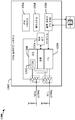
| US10031547B2 (en) | CCIe receiver logic register write only with receiver clock |
Legal Events
| Date | Code | Title | Description |
|---|---|---|---|
| PA0105 | International application |
Patent event date: 20160715 Patent event code: PA01051R01D Comment text: International Patent Application |
|
| PG1501 | Laying open of application | ||
| PC1203 | Withdrawal of no request for examination | ||
| WITN | Application deemed withdrawn, e.g. because no request for examination was filed or no examination fee was paid |